US20080241985A1 - Microelectronic imaging units and methods of manufacturing microelectronic imaging units - Google Patents
Microelectronic imaging units and methods of manufacturing microelectronic imaging unitsDownload PDFInfo
- Publication number
- US20080241985A1 US20080241985A1US12/081,003US8100308AUS2008241985A1US 20080241985 A1US20080241985 A1US 20080241985A1US 8100308 AUS8100308 AUS 8100308AUS 2008241985 A1US2008241985 A1US 2008241985A1
- Authority
- US
- United States
- Prior art keywords
- stand
- imaging
- forming
- act
- external contacts
- Prior art date
- Legal status (The legal status is an assumption and is not a legal conclusion. Google has not performed a legal analysis and makes no representation as to the accuracy of the status listed.)
- Granted
Links
- 238000003384imaging methodMethods0.000titleclaimsabstractdescription123
- 238000000034methodMethods0.000titleclaimsabstractdescription56
- 238000004519manufacturing processMethods0.000titleclaimsabstractdescription25
- 238000004377microelectronicMethods0.000titleabstractdescription36
- 239000000463materialSubstances0.000claimsdescription24
- 239000000853adhesiveSubstances0.000claimsdescription13
- 230000001070adhesive effectEffects0.000claimsdescription13
- 239000004593EpoxySubstances0.000claimsdescription5
- 238000000151depositionMethods0.000claimsdescription5
- NIXOWILDQLNWCW-UHFFFAOYSA-Nacrylic acid groupChemical groupC(C=C)(=O)ONIXOWILDQLNWCW-UHFFFAOYSA-N0.000claimsdescription2
- 238000005520cutting processMethods0.000claims3
- 238000000059patterningMethods0.000claims1
- 230000008878couplingEffects0.000abstractdescription5
- 238000010168coupling processMethods0.000abstractdescription5
- 238000005859coupling reactionMethods0.000abstractdescription5
- 230000008569processEffects0.000description7
- 230000008901benefitEffects0.000description5
- 239000000758substrateSubstances0.000description5
- 239000004065semiconductorSubstances0.000description4
- 239000000969carrierSubstances0.000description3
- 238000003491arrayMethods0.000description2
- 230000008859changeEffects0.000description2
- 230000005855radiationEffects0.000description2
- 238000001228spectrumMethods0.000description2
- 239000004642PolyimideSubstances0.000description1
- 239000002313adhesive filmSubstances0.000description1
- 230000003667anti-reflective effectEffects0.000description1
- 238000000149argon plasma sinteringMethods0.000description1
- 230000000295complement effectEffects0.000description1
- 150000001875compoundsChemical class0.000description1
- 239000000356contaminantSubstances0.000description1
- 238000005516engineering processMethods0.000description1
- 230000009969flowable effectEffects0.000description1
- 239000011521glassSubstances0.000description1
- 238000003475laminationMethods0.000description1
- 229910044991metal oxideInorganic materials0.000description1
- 150000004706metal oxidesChemical class0.000description1
- 238000012986modificationMethods0.000description1
- 230000004048modificationEffects0.000description1
- 230000003287optical effectEffects0.000description1
- 238000004806packaging method and processMethods0.000description1
- 229920001721polyimidePolymers0.000description1
- 238000007639printingMethods0.000description1
- 239000010453quartzSubstances0.000description1
- 238000007650screen-printingMethods0.000description1
- VYPSYNLAJGMNEJ-UHFFFAOYSA-Nsilicon dioxideInorganic materialsO=[Si]=OVYPSYNLAJGMNEJ-UHFFFAOYSA-N0.000description1
- 229910000679solderInorganic materials0.000description1
- 239000000126substanceSubstances0.000description1
- 238000001429visible spectrumMethods0.000description1
Images


Classifications
- H—ELECTRICITY
- H10—SEMICONDUCTOR DEVICES; ELECTRIC SOLID-STATE DEVICES NOT OTHERWISE PROVIDED FOR
- H10F—INORGANIC SEMICONDUCTOR DEVICES SENSITIVE TO INFRARED RADIATION, LIGHT, ELECTROMAGNETIC RADIATION OF SHORTER WAVELENGTH OR CORPUSCULAR RADIATION
- H10F39/00—Integrated devices, or assemblies of multiple devices, comprising at least one element covered by group H10F30/00, e.g. radiation detectors comprising photodiode arrays
- H10F39/80—Constructional details of image sensors
- H10F39/804—Containers or encapsulations
- H—ELECTRICITY
- H01—ELECTRIC ELEMENTS
- H01L—SEMICONDUCTOR DEVICES NOT COVERED BY CLASS H10
- H01L24/00—Arrangements for connecting or disconnecting semiconductor or solid-state bodies; Methods or apparatus related thereto
- H01L24/93—Batch processes
- H01L24/95—Batch processes at chip-level, i.e. with connecting carried out on a plurality of singulated devices, i.e. on diced chips
- H01L24/97—Batch processes at chip-level, i.e. with connecting carried out on a plurality of singulated devices, i.e. on diced chips the devices being connected to a common substrate, e.g. interposer, said common substrate being separable into individual assemblies after connecting
- B—PERFORMING OPERATIONS; TRANSPORTING
- B33—ADDITIVE MANUFACTURING TECHNOLOGY
- B33Y—ADDITIVE MANUFACTURING, i.e. MANUFACTURING OF THREE-DIMENSIONAL [3-D] OBJECTS BY ADDITIVE DEPOSITION, ADDITIVE AGGLOMERATION OR ADDITIVE LAYERING, e.g. BY 3-D PRINTING, STEREOLITHOGRAPHY OR SELECTIVE LASER SINTERING
- B33Y80/00—Products made by additive manufacturing
- H—ELECTRICITY
- H01—ELECTRIC ELEMENTS
- H01L—SEMICONDUCTOR DEVICES NOT COVERED BY CLASS H10
- H01L2224/00—Indexing scheme for arrangements for connecting or disconnecting semiconductor or solid-state bodies and methods related thereto as covered by H01L24/00
- H01L2224/01—Means for bonding being attached to, or being formed on, the surface to be connected, e.g. chip-to-package, die-attach, "first-level" interconnects; Manufacturing methods related thereto
- H01L2224/02—Bonding areas; Manufacturing methods related thereto
- H01L2224/04—Structure, shape, material or disposition of the bonding areas prior to the connecting process
- H01L2224/05—Structure, shape, material or disposition of the bonding areas prior to the connecting process of an individual bonding area
- H01L2224/0554—External layer
- H01L2224/0555—Shape
- H01L2224/05552—Shape in top view
- H01L2224/05554—Shape in top view being square
- H—ELECTRICITY
- H01—ELECTRIC ELEMENTS
- H01L—SEMICONDUCTOR DEVICES NOT COVERED BY CLASS H10
- H01L2224/00—Indexing scheme for arrangements for connecting or disconnecting semiconductor or solid-state bodies and methods related thereto as covered by H01L24/00
- H01L2224/01—Means for bonding being attached to, or being formed on, the surface to be connected, e.g. chip-to-package, die-attach, "first-level" interconnects; Manufacturing methods related thereto
- H01L2224/26—Layer connectors, e.g. plate connectors, solder or adhesive layers; Manufacturing methods related thereto
- H01L2224/31—Structure, shape, material or disposition of the layer connectors after the connecting process
- H01L2224/32—Structure, shape, material or disposition of the layer connectors after the connecting process of an individual layer connector
- H01L2224/321—Disposition
- H01L2224/32151—Disposition the layer connector connecting between a semiconductor or solid-state body and an item not being a semiconductor or solid-state body, e.g. chip-to-substrate, chip-to-passive
- H01L2224/32221—Disposition the layer connector connecting between a semiconductor or solid-state body and an item not being a semiconductor or solid-state body, e.g. chip-to-substrate, chip-to-passive the body and the item being stacked
- H01L2224/32225—Disposition the layer connector connecting between a semiconductor or solid-state body and an item not being a semiconductor or solid-state body, e.g. chip-to-substrate, chip-to-passive the body and the item being stacked the item being non-metallic, e.g. insulating substrate with or without metallisation
- H—ELECTRICITY
- H01—ELECTRIC ELEMENTS
- H01L—SEMICONDUCTOR DEVICES NOT COVERED BY CLASS H10
- H01L2224/00—Indexing scheme for arrangements for connecting or disconnecting semiconductor or solid-state bodies and methods related thereto as covered by H01L24/00
- H01L2224/01—Means for bonding being attached to, or being formed on, the surface to be connected, e.g. chip-to-package, die-attach, "first-level" interconnects; Manufacturing methods related thereto
- H01L2224/42—Wire connectors; Manufacturing methods related thereto
- H01L2224/47—Structure, shape, material or disposition of the wire connectors after the connecting process
- H01L2224/48—Structure, shape, material or disposition of the wire connectors after the connecting process of an individual wire connector
- H01L2224/4805—Shape
- H01L2224/4809—Loop shape
- H01L2224/48091—Arched
- H—ELECTRICITY
- H01—ELECTRIC ELEMENTS
- H01L—SEMICONDUCTOR DEVICES NOT COVERED BY CLASS H10
- H01L2224/00—Indexing scheme for arrangements for connecting or disconnecting semiconductor or solid-state bodies and methods related thereto as covered by H01L24/00
- H01L2224/01—Means for bonding being attached to, or being formed on, the surface to be connected, e.g. chip-to-package, die-attach, "first-level" interconnects; Manufacturing methods related thereto
- H01L2224/42—Wire connectors; Manufacturing methods related thereto
- H01L2224/47—Structure, shape, material or disposition of the wire connectors after the connecting process
- H01L2224/48—Structure, shape, material or disposition of the wire connectors after the connecting process of an individual wire connector
- H01L2224/481—Disposition
- H01L2224/48151—Connecting between a semiconductor or solid-state body and an item not being a semiconductor or solid-state body, e.g. chip-to-substrate, chip-to-passive
- H01L2224/48221—Connecting between a semiconductor or solid-state body and an item not being a semiconductor or solid-state body, e.g. chip-to-substrate, chip-to-passive the body and the item being stacked
- H01L2224/48225—Connecting between a semiconductor or solid-state body and an item not being a semiconductor or solid-state body, e.g. chip-to-substrate, chip-to-passive the body and the item being stacked the item being non-metallic, e.g. insulating substrate with or without metallisation
- H01L2224/48227—Connecting between a semiconductor or solid-state body and an item not being a semiconductor or solid-state body, e.g. chip-to-substrate, chip-to-passive the body and the item being stacked the item being non-metallic, e.g. insulating substrate with or without metallisation connecting the wire to a bond pad of the item
- H—ELECTRICITY
- H01—ELECTRIC ELEMENTS
- H01L—SEMICONDUCTOR DEVICES NOT COVERED BY CLASS H10
- H01L2224/00—Indexing scheme for arrangements for connecting or disconnecting semiconductor or solid-state bodies and methods related thereto as covered by H01L24/00
- H01L2224/01—Means for bonding being attached to, or being formed on, the surface to be connected, e.g. chip-to-package, die-attach, "first-level" interconnects; Manufacturing methods related thereto
- H01L2224/42—Wire connectors; Manufacturing methods related thereto
- H01L2224/47—Structure, shape, material or disposition of the wire connectors after the connecting process
- H01L2224/49—Structure, shape, material or disposition of the wire connectors after the connecting process of a plurality of wire connectors
- H01L2224/491—Disposition
- H01L2224/4912—Layout
- H01L2224/49175—Parallel arrangements
- H—ELECTRICITY
- H01—ELECTRIC ELEMENTS
- H01L—SEMICONDUCTOR DEVICES NOT COVERED BY CLASS H10
- H01L2224/00—Indexing scheme for arrangements for connecting or disconnecting semiconductor or solid-state bodies and methods related thereto as covered by H01L24/00
- H01L2224/91—Methods for connecting semiconductor or solid state bodies including different methods provided for in two or more of groups H01L2224/80 - H01L2224/90
- H01L2224/92—Specific sequence of method steps
- H01L2224/922—Connecting different surfaces of the semiconductor or solid-state body with connectors of different types
- H01L2224/9222—Sequential connecting processes
- H01L2224/92242—Sequential connecting processes the first connecting process involving a layer connector
- H01L2224/92247—Sequential connecting processes the first connecting process involving a layer connector the second connecting process involving a wire connector
- H—ELECTRICITY
- H01—ELECTRIC ELEMENTS
- H01L—SEMICONDUCTOR DEVICES NOT COVERED BY CLASS H10
- H01L2924/00—Indexing scheme for arrangements or methods for connecting or disconnecting semiconductor or solid-state bodies as covered by H01L24/00
- H01L2924/10—Details of semiconductor or other solid state devices to be connected
- H01L2924/11—Device type
- H01L2924/14—Integrated circuits
- H—ELECTRICITY
- H01—ELECTRIC ELEMENTS
- H01L—SEMICONDUCTOR DEVICES NOT COVERED BY CLASS H10
- H01L2924/00—Indexing scheme for arrangements or methods for connecting or disconnecting semiconductor or solid-state bodies as covered by H01L24/00
- H01L2924/15—Details of package parts other than the semiconductor or other solid state devices to be connected
- H01L2924/151—Die mounting substrate
- H01L2924/1517—Multilayer substrate
- H01L2924/15182—Fan-in arrangement of the internal vias
- H01L2924/15184—Fan-in arrangement of the internal vias in different layers of the multilayer substrate
- H—ELECTRICITY
- H01—ELECTRIC ELEMENTS
- H01L—SEMICONDUCTOR DEVICES NOT COVERED BY CLASS H10
- H01L2924/00—Indexing scheme for arrangements or methods for connecting or disconnecting semiconductor or solid-state bodies as covered by H01L24/00
- H01L2924/15—Details of package parts other than the semiconductor or other solid state devices to be connected
- H01L2924/161—Cap
- H01L2924/162—Disposition
- H01L2924/16235—Connecting to a semiconductor or solid-state bodies, i.e. cap-to-chip
- H—ELECTRICITY
- H01—ELECTRIC ELEMENTS
- H01L—SEMICONDUCTOR DEVICES NOT COVERED BY CLASS H10
- H01L2924/00—Indexing scheme for arrangements or methods for connecting or disconnecting semiconductor or solid-state bodies as covered by H01L24/00
- H01L2924/15—Details of package parts other than the semiconductor or other solid state devices to be connected
- H01L2924/181—Encapsulation
Definitions
- the present inventionis related to microelectronic imaging units having solid-state image sensors and methods for manufacturing such imaging units.
- Microelectronic imagersare used in digital cameras, wireless devices with picture capabilities, and many other applications.
- Cell phones and Personal Digital Assistants (PDAs)for example, are incorporating microelectronic imagers for capturing and sending pictures.
- PDAsPersonal Digital Assistants
- the growth rate of microelectronic imagershas been steadily increasing as they become smaller and produce better images with higher pixel counts.
- Microelectronic imagersinclude image sensors that use Charged Coupled Device (CCD) systems, Complementary Metal-Oxide Semiconductor (CMOS) systems, or other solid-state systems.
- CCD image sensorshave been widely used in digital cameras and other applications.
- CMOS image sensorsare also quickly becoming very popular because they are expected to have low production costs, high yields, and small sizes.
- CMOS image sensorscan provide these advantages because they are manufactured using technology and equipment developed for fabricating semiconductor devices.
- CMOS image sensors, as well as CCD image sensorsare accordingly “packaged” to protect their delicate components and to provide external electrical contacts.
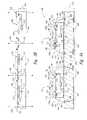
- FIG. 1is a schematic side cross-sectional view of a conventional microelectronic imaging unit 1 including an imaging die 10 , a chip carrier 30 carrying the die 10 , and a cover 50 attached to the carrier 30 and positioned over the die 10 .
- the imaging die 10includes an image sensor 12 and a plurality of bond-pads 16 operably coupled to the image sensor 12 .
- the chip carrier 30has a base 32 , sidewalls 34 projecting from the base 32 , and a recess 36 defined by the base 32 and sidewalls 34 .
- the die 10is accordingly sized to be received within the recess 36 and attached to the base 32 .
- the chip carrier 30further includes an array of terminals 18 on the base 32 , an array of contacts 24 on an external surface 38 , and a plurality of traces 22 electrically connecting the terminals 18 to corresponding external contacts 24 .
- the terminals 18are positioned between the die 10 and the sidewalls 34 so that wire-bonds 20 can electrically couple the terminals 18 to corresponding bond-pads 16 on the die 10 .
- microelectronic imaging unit 1 illustrated in FIG. 1One problem with the microelectronic imaging unit 1 illustrated in FIG. 1 is that the die 10 must be sized and configured to fit within the recess 36 of the chip carrier 30 . Dies having different shapes and/or sizes accordingly require chip carriers configured to house those specific types of dies. As such, manufacturing imaging units with dies having different sizes requires fabricating various configurations of chip carriers and significantly retooling the manufacturing process.
- the footprint of the imaging unit 1 in FIG. 1is the surface area of the base 32 of the chip carrier 30 , which is significantly larger than the surface area of the die 10 . Accordingly, the footprint of conventional microelectronic imaging units can be a limiting factor in the design and marketability of picture cell phones or PDAs because these devices are continually being made smaller in order to be more portable. Therefore, there is a need to provide microelectronic imaging units with smaller footprints.
- FIG. 1is a schematic side cross-sectional view of a conventional microelectronic imaging unit in accordance with the prior art.
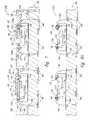
- FIGS. 2-5illustrate stages in one embodiment of a method for manufacturing a plurality of microelectronic imaging units in accordance with the invention.
- FIG. 2is a schematic side cross-sectional view of a microfeature workpiece having a substrate and a plurality of microelectronic imaging dies formed in and/or on the substrate.
- FIG. 3Ais a top plan view of the microfeature workpiece after forming a plurality of openings in a stand-off layer.
- FIG. 3Bis a schematic side cross-sectional view taken substantially along line A-A of FIG. 3A .
- FIG. 4Ais a schematic side cross-sectional view of an assembly including a plurality of singulated microelectronic imaging dies arranged in an array on a support member.
- FIG. 4Bis a top plan view of the assembly illustrated in FIG. 4A .
- FIG. 5is a schematic side cross-sectional view of the assembly after attaching a plurality of covers to corresponding stand-offs.
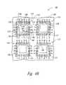
- FIGS. 6A-7illustrate stages in another embodiment of a method for manufacturing a plurality of microelectronic imaging units in accordance with the invention.
- FIG. 6Ais a schematic side cross-sectional view of an assembly including a plurality of microelectronic imaging dies arranged in an array on a support member.
- FIG. 6Bis a top plan view of the assembly of FIG. 6A .
- FIG. 7is a schematic side cross-sectional view of the assembly after wire-bonding the imaging dies to the support member and attaching a plurality of covers to corresponding dies.
- FIGS. 8A-9illustrate stages in another embodiment of a method for manufacturing a plurality of microelectronic imaging units in accordance with the invention.
- FIG. 8Ais a schematic side cross-sectional view of an assembly including a plurality of imaging dies arranged in an array on a support member.
- FIG. 8Bis a top plan view of the assembly of FIG. 8A .
- FIG. 9is a schematic side cross-sectional view of the assembly after attaching a plurality of covers to corresponding imaging dies.
- One aspect of the inventionis directed toward methods for manufacturing a plurality of imaging units.
- An embodiment of one such methodincludes coupling a plurality of singulated imaging dies to a support member.
- the individual imaging dieshave an image sensor, an integrated circuit operably coupled to the image sensor, and a plurality of external contacts operably coupled to the integrated circuit.
- the methodfurther includes forming a plurality of stand-offs on corresponding imaging dies before and/or after the imaging dies are singulated and electrically connecting the external contacts of the imaging dies to corresponding terminals on the support member.
- the individual stand-offsinclude a portion between adjacent external contacts.
- a methodin another embodiment, includes providing a plurality of imaging dies.
- the individual imaging dieshave an image sensor, an integrated circuit operably coupled to the image sensor, and a plurality of external contacts operably coupled to the integrated circuit.
- the methodfurther includes constructing a plurality of stand-offs on corresponding imaging dies so that the individual stand-offs form a perimeter around an associated image sensor and attaching the imaging dies to a support member.
- the methodfurther includes electrically connecting the external contacts of the imaging dies to corresponding terminals on the support member and coupling a plurality of covers to corresponding imaging dies. The covers are carried by the stand-offs and positioned over corresponding image sensors.
- an assembly of microelectronic imaging unitsincludes a support member and a plurality of imaging dies attached to the support member.
- the individual imaging dieshave an image sensor, an integrated circuit operably coupled to the image sensor, and a plurality of external contacts operably coupled to the integrated circuit.
- the assemblyfurther includes (a) a plurality of stand-offs on corresponding imaging dies outboard the image sensors and (b) a plurality of covers coupled to corresponding stand-offs and positioned over the associated image sensors.
- the individual stand-offsinclude at least a portion inboard the external contacts.
- CMOS imaging unitsto provide a thorough understanding of these embodiments, but other embodiments can use CCD imaging units or other types of solid-state imaging devices.
- CCD imaging unitsor other types of solid-state imaging devices.
- Several details describing structures or processes that are well known and often associated with other types of microelectronic devicesare not set forth in the following description for purposes of brevity.
- the following disclosuresets forth several embodiments of different aspects of the invention, several other embodiments of the invention can have different configurations or different components than those described in this section. As such, it should be understood that the invention may have other embodiments with additional elements or without several of the elements described below with reference to FIGS. 2-9 .
- FIGS. 2-5illustrate stages in one embodiment of a method for manufacturing a plurality of microelectronic imaging units.
- FIG. 2is a schematic side cross-sectional view of a microfeature workpiece 104 having a substrate 105 and a plurality of microelectronic imaging dies 110 (only three are shown) formed in and/or on the substrate 105 .
- the individual imaging dies 110include an image sensor 112 , an integrated circuit 114 (shown schematically) operably coupled to the image sensor 112 , and a plurality of external contacts 116 (e.g., bond-pads) operably coupled to the integrated circuit 114 .
- the image sensors 112can be CMOS devices or CCD image sensors for capturing pictures or other images in the visible spectrum.
- the image sensors 112may also detect radiation in other spectrums (e.g., IR or UV ranges).
- a stand-off layer 132is formed across the microfeature workpiece 104 .
- the stand-off layer 132can be formed on the workpiece 104 by spin-on, film lamination, or other suitable processes.
- the stand-off layer 132has a precise thickness T, which corresponds to a desired distance between the image sensors 112 and corresponding covers ( FIG. 5 ), which are placed over the image sensors 112 as described in greater detail below.
- FIG. 3Ais a top plan view of the microfeature workpiece 104 after forming a plurality of openings 133 and 134 in the stand-off layer 132 .
- FIG. 3Bis a schematic side cross-sectional view taken substantially along line A-A of FIG. 3A .
- the illustrated openings 133expose corresponding image sensors 112 and a portion of a first surface 106 of the workpiece 104 outboard the image sensors 112 .
- the openings 133may not expose a portion of the first surface 106 outboard the image sensors 112 .
- the individual openings 134expose adjacent external contacts 116 of adjoining imaging dies 110 . In additional embodiments, such as those described below with reference to FIGS. 6A-7 , the individual openings 134 may expose only a single contact 116 .
- the stand-off layer 132can include an epoxy, a polyimide, or another suitable photo-patternable material.
- the openings 133 and 134are formed by placing a mask on the stand-off layer 132 , exposing and developing the mask, and removing portions of the layer 132 over the image sensors 112 and the contacts 116 .
- the openings 133 and 134can be formed by stamping, imprinting, or other suitable processes.
- a stand-off layercan be formed with the openings 133 and 134 by stereolithography, screen printing, stencil printing, or other suitable techniques.
- the microfeature workpiece 104can be cut along lines B-B ( FIG. 3B ) by scribing, sawing, or other suitable processes to singulate the individual imaging dies 110 .
- FIG. 4Ais a schematic side cross-sectional view of an assembly 100 including the singulated microelectronic imaging dies 110 (only two are shown) arranged in an array on a support member 160 .
- the individual singulated imaging dies 110include a first side 111 , a second side 113 opposite the first side 111 , and a plurality of ends 115 extending from the first side 111 to the second side 113 .
- the second side 113 of the imaging dies 110is attached to the support member 160 with an adhesive 120 , such as an adhesive film, epoxy, or other suitable material.
- the support member 160can be a lead frame or a substrate, such as a printed circuit board, for carrying the imaging dies 110 .
- the support member 160includes a first side 162 having a plurality of terminals 166 and a second side 164 having a plurality of pads 168 .
- the terminals 166can be arranged in arrays for attachment to corresponding external contacts 116 of the dies 110
- the pads 168can be arranged in arrays for attachment to a plurality of conductive couplers (e.g., solder balls).
- the support member 160further includes a plurality of conductive traces 169 electrically coupling the terminals 166 to corresponding pads 168 .
- FIG. 4Bis a top plan view of the assembly 100 illustrated in FIG. 4A .
- the individual imaging dies 110include a corresponding stand-off 130 projecting from the first side 111 .
- the individual stand-offs 130include a plurality of openings 134 a over corresponding contacts 116 , a first portion 136 directly between adjacent contacts 116 , and a second portion 138 inboard the contacts 116 and outboard the image sensor 112 .
- the illustrated openings 134 aare slots with an open end proximate to the end 115 of the die 110 .
- the first portion 136 of the stand-offs 130separates adjacent slots, and the second portion 138 forms a perimeter around the corresponding image sensor 112 .
- the illustrated stand-offs 130also have a generally flat top surface 131 for supporting covers ( FIG. 5 ) and a height T ( FIG. 4A ) that corresponds to a precise distance between the image sensors 112 and the covers, as described below with reference to FIG. 5 .
- the stand-offs 130can have other configurations.
- the stand-offsmay not include the first portion 136 between adjacent contacts 116 , but rather the stand-offs may be entirely inboard the contacts 116 and outboard the image sensors 112 .
- the top surface of the stand-offsmay not be flat and/or the openings can be holes rather than slots, as described in greater detail below with reference to FIGS. 6A-7 .
- the illustrated assembly 100further includes a plurality of wire-bonds 140 electrically coupling the external contacts 116 of the imaging dies 110 to corresponding terminals 166 on the support member 160 .
- the individual wire-bonds 140include (a) a proximal portion 142 attached to one of the contacts 116 and received in a corresponding opening 134 a and (b) a distal portion 144 attached to the corresponding terminal 166 .
- the external contacts 116can be electrically connected to the terminals on a support member by conductive through-wafer interconnects. Through-wafer interconnects are described in U.S.
- FIG. 5is a schematic side cross-sectional view of the assembly 100 after (a) attaching a plurality of covers 150 to corresponding stand-offs 130 and (b) depositing a fill material 180 onto the support member 160 between adjacent dies 110 .
- the covers 150can be attached to the top surface 131 of the stand-offs 130 with an adhesive 151 , such as epoxy or acrylic.
- the stand-offs 130can be formed of an adhesive material so that an additional adhesive is unnecessary.
- the individual covers 150are positioned over corresponding image sensors 112 and can be glass, quartz, or another suitable material that is transmissive to the desired spectrum of radiation.
- the covers 150for example, can further include one or more anti-reflective films and/or filters.
- the individual covers 150are spaced apart from the image sensors 112 by a predetermined and precise distance G, which corresponds to the height T ( FIG. 4A ) of the stand-offs 130 . Accordingly, the covers 150 , the stand-offs 130 , and the first side 111 of the dies 110 define cells 152 , which can be filled with gas, such as air, or an underfill material, as described below with reference to FIG. 7 .
- the assembly 100can include a single cover attached to multiple stand-offs 130 and covering several imaging dies 110 .
- the stand-offs 130can be formed on the covers 150 rather than the imaging dies 110 , as described above with reference to FIGS. 2-3B . In such embodiments, after forming the stand-offs 130 on the covers 150 , pairs of stand-offs 130 and covers 150 can be attached as units to corresponding imaging dies 110 .
- the fill material 180is dispensed onto the support member 160 between adjacent imaging dies 110 .
- the fill material 180can be an epoxy mold compound or another suitable material to at least partially encapsulate the imaging dies 110 , the stand-offs 130 , the wire-bonds 140 , and the covers 150 .
- the fill material 180(a) increases the robustness of the assembly 100 , (b) enhances the integrity of the joint between the individual covers 150 and the imaging dies 110 , and (c) protects the image sensors 112 from moisture, chemicals, and other contaminants.
- the assembly 100can be heated to at least partially cure (i.e., B-stage) the fill material 180 , the adhesive 151 , and/or the stand-offs 130 . After curing, the assembly 100 can be cut along lines C-C to singulate individual imaging units 102 .
- One feature of the imaging units 102 illustrated in FIG. 5is that the stand-offs 130 are attached to the imaging dies 110 .
- An advantage of this featureis that the footprint of the individual imaging units 102 is smaller than the footprint of conventional imaging units.
- the reduced footprint of the imaging units 102is particularly advantageous for picture cell phones, PDAs, or other applications where space is limited.
- the sidewalls 34 of the chip carrier 30are outboard the terminals 18 and the wire-bonds 20 , which increases the footprint of the imaging unit 1 .
- One feature of the method for manufacturing imaging units 102 illustrated in FIGS. 2-5is that the support member 160 can carry imaging dies 110 with different sizes and/or configurations.
- An advantage of this featureis that the method can be easily adapted to handle various configurations of imaging dies without significant changes to the fabrication process.
- Prior art methodssuch as the method required to form the imaging unit 1 described above with reference to FIG. 1 , may require significant retooling because the chip carriers 30 can only carry imaging dies 10 with a certain shape and size.
- Another advantage of the method for manufacturing imaging units 102 illustrated in FIGS. 2-5is that the method is expected to significantly enhance the efficiency of the manufacturing process because a plurality of imaging units 102 can be fabricated simultaneously using highly accurate and efficient processes developed for packaging and manufacturing semiconductor devices.
- This method of manufacturing imaging units 102is also expected to enhance the quality and performance of the imaging units 102 because the semiconductor fabrication processes can reliably produce and assemble the various components with a high degree of precision.
- several embodiments of the methodare expected to significantly reduce the cost for assembling microelectronic imaging units 102 , increase the performance of the imaging units 102 , and produce higher quality imaging units 102 .
- FIGS. 6A-7illustrate stages in another embodiment of a method for manufacturing a plurality of microelectronic imaging units 202 in accordance with the invention.
- FIG. 6Ais a schematic side cross-sectional view
- FIG. 6Bis a top plan view of an assembly 200 including a plurality of microelectronic imaging dies 110 (only two shown) arranged in an array on a support member 160 .
- the illustrated assembly 200is generally similar to the assembly 100 described above with reference to FIGS. 4A and 4B .
- the illustrated assembly 200includes a plurality of stand-offs 230 disposed on corresponding imaging dies 110 .
- the illustrated stand-offs 230include a first portion 236 ( FIG.
- the stand-offs 230also have a height D 1 , an arcuate top surface 231 ( FIG. 6A ), and a plurality of openings 234 a between the second and third portions 237 and 238 .
- the illustrated openings 234 aare holes aligned with corresponding external contacts 116 and positioned toward an outer portion of the stand-offs 230 .
- the openings 234 ainclude an outer wall 233 with a height D 2 ( FIG. 6A ) and an inner wall 239 with a height D 3 ( FIG. 6A ) greater than the height D 2 of the outer wall 233 .
- FIG. 7is a schematic side cross-sectional view of the assembly 200 after wire-bonding the imaging dies 110 to the support member 160 and attaching a plurality of covers 150 to corresponding dies 110 .
- the individual wire-bonds 140include (a) a proximal portion 142 attached to one of the external contacts 116 and received in a corresponding opening 234 a and (b) a distal portion 144 attached to the corresponding terminal 166 .
- the wire-bonds 140can be formed so that they do not project above the height D 1 of the stand-offs 230 and interfere with the attachment of the covers 150 to the top surface 231 of the stand-offs 230 .
- the covers 150can be attached to corresponding stand-offs 230 with an adhesive, or, alternatively, the stand-offs 230 can be made of an adhesive material.
- the illustrated assembly 200can optionally include an underfill 254 disposed across the first side 111 of the imaging dies 110 .
- the underfill 254covers the image sensors 112 and fills the cells 152 between the covers 150 and the imaging dies 110 .
- the underfill 254can be an optical grade material with a high transparency to eliminate or reduce light scattering and/or the loss of images. In applications in which the image sensor 112 has pixels with a smaller size, the underfill 254 can have a higher refractive index to assist in focusing the light for the pixels.
- the underfill 254can be a material that is dimensionally stable over a wide range of temperatures.
- An advantage of this featureis that the distance between the covers 150 and the corresponding image sensors 112 remains generally consistent, even if the imaging units 202 operate in an environment that experiences significant changes in ambient temperature. If the temperature change were to cause the medium between the cover 150 and the image sensor 112 to expand or contract, the associated change in the distance between the cover 150 and the image sensor 112 could skew the images and reduce the life of the imaging unit 202 due to fatigue.
- FIGS. 8A-9illustrate stages in another embodiment of a method for manufacturing a plurality of microelectronic imaging units 302 in accordance with the invention.
- FIG. 8Ais a schematic side cross-sectional view
- FIG. 8Bis a top plan view of an assembly 300 including a plurality of imaging dies 110 (only two shown) arranged in an array on a support member 160 .
- the illustrated assembly 300is generally similar to the assembly 200 described above with reference to FIGS. 6A and 6B .
- the illustrated assembly 300includes a plurality of stand-offs 330 disposed on corresponding imaging dies 110 .
- the illustrated stand-offs 330do not include openings, but rather encapsulate the proximal portion 142 of the individual wire-bonds 140 .
- the stand-offs 330can be formed by dispensing a flowable material onto the imaging dies 110 after wire-bonding the dies 110 to the support member 160 .
- the stand-offs 330are disposed over the external contacts 116 , in other embodiments, the stand-offs 330 can be inboard or outboard the contacts 116 .
- FIG. 9is a schematic side cross-sectional view of the assembly 300 after attaching a plurality of covers 150 to corresponding imaging dies 110 .
- the covers 150can be attached directly to the stand-offs 330 in embodiments in which the stand-offs 330 include an adhesive material.
- the stand-offs 330can include a UV- or thermally-curable adhesive material.
- an adhesivecan be placed on a perimeter portion of the covers 150 and/or a top surface of the stand-offs 330 to adhere the covers 150 to the stand-offs 330 .
- the stand-offs 330can be formed on the covers 150 and then the covers 150 and the stand-offs 330 can be attached as units to the imaging dies 110 .
- microelectronic imaging unitscan have any combination of the features described above. Accordingly, the invention is not limited except as by the appended claims.
Landscapes
- Engineering & Computer Science (AREA)
- Computer Hardware Design (AREA)
- Microelectronics & Electronic Packaging (AREA)
- Power Engineering (AREA)
- Solid State Image Pick-Up Elements (AREA)
Abstract
Description
- The present invention is related to microelectronic imaging units having solid-state image sensors and methods for manufacturing such imaging units.
- Microelectronic imagers are used in digital cameras, wireless devices with picture capabilities, and many other applications. Cell phones and Personal Digital Assistants (PDAs), for example, are incorporating microelectronic imagers for capturing and sending pictures. The growth rate of microelectronic imagers has been steadily increasing as they become smaller and produce better images with higher pixel counts.
- Microelectronic imagers include image sensors that use Charged Coupled Device (CCD) systems, Complementary Metal-Oxide Semiconductor (CMOS) systems, or other solid-state systems. CCD image sensors have been widely used in digital cameras and other applications. CMOS image sensors are also quickly becoming very popular because they are expected to have low production costs, high yields, and small sizes. CMOS image sensors can provide these advantages because they are manufactured using technology and equipment developed for fabricating semiconductor devices. CMOS image sensors, as well as CCD image sensors, are accordingly “packaged” to protect their delicate components and to provide external electrical contacts.
FIG. 1 is a schematic side cross-sectional view of a conventionalmicroelectronic imaging unit 1 including animaging die 10, achip carrier 30 carrying the die10, and acover 50 attached to thecarrier 30 and positioned over the die10. The imaging die10 includes animage sensor 12 and a plurality of bond-pads 16 operably coupled to theimage sensor 12. Thechip carrier 30 has abase 32,sidewalls 34 projecting from thebase 32, and arecess 36 defined by thebase 32 andsidewalls 34. The die10 is accordingly sized to be received within therecess 36 and attached to thebase 32. Thechip carrier 30 further includes an array ofterminals 18 on thebase 32, an array ofcontacts 24 on anexternal surface 38, and a plurality oftraces 22 electrically connecting theterminals 18 to correspondingexternal contacts 24. Theterminals 18 are positioned between the die10 and thesidewalls 34 so that wire-bonds 20 can electrically couple theterminals 18 to corresponding bond-pads 16 on the die10.- One problem with the
microelectronic imaging unit 1 illustrated inFIG. 1 is that the die10 must be sized and configured to fit within therecess 36 of thechip carrier 30. Dies having different shapes and/or sizes accordingly require chip carriers configured to house those specific types of dies. As such, manufacturing imaging units with dies having different sizes requires fabricating various configurations of chip carriers and significantly retooling the manufacturing process. - Another problem with conventional microelectronic imaging units is that they have relatively large footprints. For example, the footprint of the
imaging unit 1 inFIG. 1 is the surface area of thebase 32 of thechip carrier 30, which is significantly larger than the surface area of thedie 10. Accordingly, the footprint of conventional microelectronic imaging units can be a limiting factor in the design and marketability of picture cell phones or PDAs because these devices are continually being made smaller in order to be more portable. Therefore, there is a need to provide microelectronic imaging units with smaller footprints. FIG. 1 is a schematic side cross-sectional view of a conventional microelectronic imaging unit in accordance with the prior art.FIGS. 2-5 illustrate stages in one embodiment of a method for manufacturing a plurality of microelectronic imaging units in accordance with the invention.FIG. 2 is a schematic side cross-sectional view of a microfeature workpiece having a substrate and a plurality of microelectronic imaging dies formed in and/or on the substrate.FIG. 3A is a top plan view of the microfeature workpiece after forming a plurality of openings in a stand-off layer.FIG. 3B is a schematic side cross-sectional view taken substantially along line A-A ofFIG. 3A .FIG. 4A is a schematic side cross-sectional view of an assembly including a plurality of singulated microelectronic imaging dies arranged in an array on a support member.FIG. 4B is a top plan view of the assembly illustrated inFIG. 4A .FIG. 5 is a schematic side cross-sectional view of the assembly after attaching a plurality of covers to corresponding stand-offs.FIGS. 6A-7 illustrate stages in another embodiment of a method for manufacturing a plurality of microelectronic imaging units in accordance with the invention.FIG. 6A is a schematic side cross-sectional view of an assembly including a plurality of microelectronic imaging dies arranged in an array on a support member.FIG. 6B is a top plan view of the assembly ofFIG. 6A .FIG. 7 is a schematic side cross-sectional view of the assembly after wire-bonding the imaging dies to the support member and attaching a plurality of covers to corresponding dies.FIGS. 8A-9 illustrate stages in another embodiment of a method for manufacturing a plurality of microelectronic imaging units in accordance with the invention.FIG. 8A is a schematic side cross-sectional view of an assembly including a plurality of imaging dies arranged in an array on a support member.FIG. 8B is a top plan view of the assembly ofFIG. 8A .FIG. 9 is a schematic side cross-sectional view of the assembly after attaching a plurality of covers to corresponding imaging dies.- The following disclosure describes several embodiments of methods for manufacturing microelectronic imaging units and microelectronic imaging units that are formed using such methods. One aspect of the invention is directed toward methods for manufacturing a plurality of imaging units. An embodiment of one such method includes coupling a plurality of singulated imaging dies to a support member. The individual imaging dies have an image sensor, an integrated circuit operably coupled to the image sensor, and a plurality of external contacts operably coupled to the integrated circuit. The method further includes forming a plurality of stand-offs on corresponding imaging dies before and/or after the imaging dies are singulated and electrically connecting the external contacts of the imaging dies to corresponding terminals on the support member. The individual stand-offs include a portion between adjacent external contacts.
- In another embodiment, a method includes providing a plurality of imaging dies. The individual imaging dies have an image sensor, an integrated circuit operably coupled to the image sensor, and a plurality of external contacts operably coupled to the integrated circuit. The method further includes constructing a plurality of stand-offs on corresponding imaging dies so that the individual stand-offs form a perimeter around an associated image sensor and attaching the imaging dies to a support member. The method further includes electrically connecting the external contacts of the imaging dies to corresponding terminals on the support member and coupling a plurality of covers to corresponding imaging dies. The covers are carried by the stand-offs and positioned over corresponding image sensors.
- Another aspect of the invention is directed toward microelectronic imaging units. In one embodiment, an assembly of microelectronic imaging units includes a support member and a plurality of imaging dies attached to the support member. The individual imaging dies have an image sensor, an integrated circuit operably coupled to the image sensor, and a plurality of external contacts operably coupled to the integrated circuit. The assembly further includes (a) a plurality of stand-offs on corresponding imaging dies outboard the image sensors and (b) a plurality of covers coupled to corresponding stand-offs and positioned over the associated image sensors. The individual stand-offs include at least a portion inboard the external contacts.
- Specific details of several embodiments of the invention are described below with reference to CMOS imaging units to provide a thorough understanding of these embodiments, but other embodiments can use CCD imaging units or other types of solid-state imaging devices. Several details describing structures or processes that are well known and often associated with other types of microelectronic devices are not set forth in the following description for purposes of brevity. Moreover, although the following disclosure sets forth several embodiments of different aspects of the invention, several other embodiments of the invention can have different configurations or different components than those described in this section. As such, it should be understood that the invention may have other embodiments with additional elements or without several of the elements described below with reference to
FIGS. 2-9 . FIGS. 2-5 illustrate stages in one embodiment of a method for manufacturing a plurality of microelectronic imaging units.FIG. 2 , for example, is a schematic side cross-sectional view of amicrofeature workpiece 104 having asubstrate 105 and a plurality of microelectronic imaging dies110 (only three are shown) formed in and/or on thesubstrate 105. The individual imaging dies110 include animage sensor 112, an integrated circuit114 (shown schematically) operably coupled to theimage sensor 112, and a plurality of external contacts116 (e.g., bond-pads) operably coupled to theintegrated circuit 114. Theimage sensors 112 can be CMOS devices or CCD image sensors for capturing pictures or other images in the visible spectrum. Theimage sensors 112 may also detect radiation in other spectrums (e.g., IR or UV ranges).- After forming the imaging dies110, a stand-
off layer 132 is formed across themicrofeature workpiece 104. The stand-off layer 132 can be formed on theworkpiece 104 by spin-on, film lamination, or other suitable processes. The stand-off layer 132 has a precise thickness T, which corresponds to a desired distance between theimage sensors 112 and corresponding covers (FIG. 5 ), which are placed over theimage sensors 112 as described in greater detail below. FIG. 3A is a top plan view of themicrofeature workpiece 104 after forming a plurality ofopenings off layer 132.FIG. 3B is a schematic side cross-sectional view taken substantially along line A-A ofFIG. 3A . Referring to bothFIGS. 3A and 3B , the illustratedopenings 133 expose correspondingimage sensors 112 and a portion of afirst surface 106 of theworkpiece 104 outboard theimage sensors 112. In several embodiments, theopenings 133 may not expose a portion of thefirst surface 106 outboard theimage sensors 112. In the illustrated embodiment, theindividual openings 134 expose adjacentexternal contacts 116 of adjoining imaging dies110. In additional embodiments, such as those described below with reference toFIGS. 6A-7 , theindividual openings 134 may expose only asingle contact 116.- The stand-
off layer 132 can include an epoxy, a polyimide, or another suitable photo-patternable material. In such embodiments, theopenings off layer 132, exposing and developing the mask, and removing portions of thelayer 132 over theimage sensors 112 and thecontacts 116. In other embodiments, theopenings openings off layer 132 and theopenings microfeature workpiece 104 can be cut along lines B-B (FIG. 3B ) by scribing, sawing, or other suitable processes to singulate the individual imaging dies110. FIG. 4A is a schematic side cross-sectional view of anassembly 100 including the singulated microelectronic imaging dies110 (only two are shown) arranged in an array on asupport member 160. The individual singulated imaging dies110 include afirst side 111, asecond side 113 opposite thefirst side 111, and a plurality ofends 115 extending from thefirst side 111 to thesecond side 113. Thesecond side 113 of the imaging dies110 is attached to thesupport member 160 with an adhesive120, such as an adhesive film, epoxy, or other suitable material.- The
support member 160 can be a lead frame or a substrate, such as a printed circuit board, for carrying the imaging dies110. In the illustrated embodiment, thesupport member 160 includes afirst side 162 having a plurality ofterminals 166 and asecond side 164 having a plurality ofpads 168. Theterminals 166 can be arranged in arrays for attachment to correspondingexternal contacts 116 of the dies110, and thepads 168 can be arranged in arrays for attachment to a plurality of conductive couplers (e.g., solder balls). Thesupport member 160 further includes a plurality ofconductive traces 169 electrically coupling theterminals 166 tocorresponding pads 168. FIG. 4B is a top plan view of theassembly 100 illustrated inFIG. 4A . Referring to bothFIGS. 4A and 4B , the individual imaging dies110 include a corresponding stand-off130 projecting from thefirst side 111. The individual stand-offs 130 include a plurality ofopenings 134aovercorresponding contacts 116, afirst portion 136 directly betweenadjacent contacts 116, and asecond portion 138 inboard thecontacts 116 and outboard theimage sensor 112. The illustratedopenings 134aare slots with an open end proximate to theend 115 of thedie 110. Accordingly, thefirst portion 136 of the stand-offs 130 separates adjacent slots, and thesecond portion 138 forms a perimeter around thecorresponding image sensor 112. The illustrated stand-offs 130 also have a generally flattop surface 131 for supporting covers (FIG. 5 ) and a height T (FIG. 4A ) that corresponds to a precise distance between theimage sensors 112 and the covers, as described below with reference toFIG. 5 . In additional embodiments, the stand-offs 130 can have other configurations. For example, the stand-offs may not include thefirst portion 136 betweenadjacent contacts 116, but rather the stand-offs may be entirely inboard thecontacts 116 and outboard theimage sensors 112. Moreover, the top surface of the stand-offs may not be flat and/or the openings can be holes rather than slots, as described in greater detail below with reference toFIGS. 6A-7 .- The illustrated
assembly 100 further includes a plurality of wire-bonds 140 electrically coupling theexternal contacts 116 of the imaging dies110 tocorresponding terminals 166 on thesupport member 160. The individual wire-bonds 140 include (a) aproximal portion 142 attached to one of thecontacts 116 and received in acorresponding opening 134aand (b) adistal portion 144 attached to thecorresponding terminal 166. In other embodiments, theexternal contacts 116 can be electrically connected to the terminals on a support member by conductive through-wafer interconnects. Through-wafer interconnects are described in U.S. patent application Ser. No. 10/713,878, filed on Nov. 13, 2003, which is hereby incorporated by reference. FIG. 5 is a schematic side cross-sectional view of theassembly 100 after (a) attaching a plurality ofcovers 150 to corresponding stand-offs 130 and (b) depositing afill material 180 onto thesupport member 160 between adjacent dies110. Thecovers 150 can be attached to thetop surface 131 of the stand-offs 130 with an adhesive151, such as epoxy or acrylic. Alternatively, the stand-offs 130 can be formed of an adhesive material so that an additional adhesive is unnecessary. In either case, the individual covers150 are positioned overcorresponding image sensors 112 and can be glass, quartz, or another suitable material that is transmissive to the desired spectrum of radiation. Thecovers 150, for example, can further include one or more anti-reflective films and/or filters. The individual covers150 are spaced apart from theimage sensors 112 by a predetermined and precise distance G, which corresponds to the height T (FIG. 4A ) of the stand-offs 130. Accordingly, thecovers 150, the stand-offs 130, and thefirst side 111 of the dies110 definecells 152, which can be filled with gas, such as air, or an underfill material, as described below with reference toFIG. 7 . In other embodiments, theassembly 100 can include a single cover attached to multiple stand-offs 130 and covering several imaging dies110. In several embodiments, the stand-offs 130 can be formed on thecovers 150 rather than the imaging dies110, as described above with reference toFIGS. 2-3B . In such embodiments, after forming the stand-offs 130 on thecovers 150, pairs of stand-offs 130 and covers150 can be attached as units to corresponding imaging dies110.- After attaching the
covers 150 to the stand-offs 130, thefill material 180 is dispensed onto thesupport member 160 between adjacent imaging dies110. Thefill material 180 can be an epoxy mold compound or another suitable material to at least partially encapsulate the imaging dies110, the stand-offs 130, the wire-bonds 140, and thecovers 150. As such, the fill material180 (a) increases the robustness of theassembly 100, (b) enhances the integrity of the joint between the individual covers150 and the imaging dies110, and (c) protects theimage sensors 112 from moisture, chemicals, and other contaminants. After depositing thefill material 180 onto thesupport member 160, theassembly 100 can be heated to at least partially cure (i.e., B-stage) thefill material 180, the adhesive151, and/or the stand-offs 130. After curing, theassembly 100 can be cut along lines C-C to singulateindividual imaging units 102. - One feature of the
imaging units 102 illustrated inFIG. 5 is that the stand-offs 130 are attached to the imaging dies110. An advantage of this feature is that the footprint of theindividual imaging units 102 is smaller than the footprint of conventional imaging units. The reduced footprint of theimaging units 102 is particularly advantageous for picture cell phones, PDAs, or other applications where space is limited. In prior art devices, such as theimaging unit 1 illustrated inFIG. 1 , thesidewalls 34 of thechip carrier 30 are outboard theterminals 18 and the wire-bonds 20, which increases the footprint of theimaging unit 1. - One feature of the method for manufacturing
imaging units 102 illustrated inFIGS. 2-5 is that thesupport member 160 can carry imaging dies110 with different sizes and/or configurations. An advantage of this feature is that the method can be easily adapted to handle various configurations of imaging dies without significant changes to the fabrication process. Prior art methods, such as the method required to form theimaging unit 1 described above with reference toFIG. 1 , may require significant retooling because thechip carriers 30 can only carry imaging dies10 with a certain shape and size. - Another advantage of the method for manufacturing
imaging units 102 illustrated inFIGS. 2-5 is that the method is expected to significantly enhance the efficiency of the manufacturing process because a plurality ofimaging units 102 can be fabricated simultaneously using highly accurate and efficient processes developed for packaging and manufacturing semiconductor devices. This method ofmanufacturing imaging units 102 is also expected to enhance the quality and performance of theimaging units 102 because the semiconductor fabrication processes can reliably produce and assemble the various components with a high degree of precision. As such, several embodiments of the method are expected to significantly reduce the cost for assemblingmicroelectronic imaging units 102, increase the performance of theimaging units 102, and produce higherquality imaging units 102. FIGS. 6A-7 illustrate stages in another embodiment of a method for manufacturing a plurality ofmicroelectronic imaging units 202 in accordance with the invention. For example,FIG. 6A is a schematic side cross-sectional view andFIG. 6B is a top plan view of anassembly 200 including a plurality of microelectronic imaging dies110 (only two shown) arranged in an array on asupport member 160. The illustratedassembly 200 is generally similar to theassembly 100 described above with reference toFIGS. 4A and 4B . For example, the illustratedassembly 200 includes a plurality of stand-offs 230 disposed on corresponding imaging dies110. The illustrated stand-offs 230 include a first portion236 (FIG. 6B ) betweenadjacent contacts 116, asecond portion 237 outboard theexternal contacts 116, and athird portion 238 inboard theexternal contacts 116. The stand-offs 230 also have a height D1, an arcuate top surface231 (FIG. 6A ), and a plurality ofopenings 234abetween the second andthird portions openings 234aare holes aligned with correspondingexternal contacts 116 and positioned toward an outer portion of the stand-offs 230. As such, theopenings 234ainclude anouter wall 233 with a height D2(FIG. 6A ) and aninner wall 239 with a height D3(FIG. 6A ) greater than the height D2of theouter wall 233.FIG. 7 is a schematic side cross-sectional view of theassembly 200 after wire-bonding the imaging dies110 to thesupport member 160 and attaching a plurality ofcovers 150 to corresponding dies110. The individual wire-bonds 140 include (a) aproximal portion 142 attached to one of theexternal contacts 116 and received in acorresponding opening 234aand (b) adistal portion 144 attached to thecorresponding terminal 166. Because the height D1of the stand-offs 230 exceeds the height D2of theouter wall 233 of theopenings 234a, the wire-bonds 140 can be formed so that they do not project above the height D1of the stand-offs 230 and interfere with the attachment of thecovers 150 to thetop surface 231 of the stand-offs 230. Thecovers 150 can be attached to corresponding stand-offs 230 with an adhesive, or, alternatively, the stand-offs 230 can be made of an adhesive material.- The illustrated
assembly 200 can optionally include anunderfill 254 disposed across thefirst side 111 of the imaging dies110. As such, theunderfill 254 covers theimage sensors 112 and fills thecells 152 between thecovers 150 and the imaging dies110. Theunderfill 254 can be an optical grade material with a high transparency to eliminate or reduce light scattering and/or the loss of images. In applications in which theimage sensor 112 has pixels with a smaller size, theunderfill 254 can have a higher refractive index to assist in focusing the light for the pixels. - One feature of the
imaging units 202 illustrated inFIG. 7 is that theunderfill 254 can be a material that is dimensionally stable over a wide range of temperatures. An advantage of this feature is that the distance between thecovers 150 and thecorresponding image sensors 112 remains generally consistent, even if theimaging units 202 operate in an environment that experiences significant changes in ambient temperature. If the temperature change were to cause the medium between thecover 150 and theimage sensor 112 to expand or contract, the associated change in the distance between thecover 150 and theimage sensor 112 could skew the images and reduce the life of theimaging unit 202 due to fatigue. FIGS. 8A-9 illustrate stages in another embodiment of a method for manufacturing a plurality ofmicroelectronic imaging units 302 in accordance with the invention. For example,FIG. 8A is a schematic side cross-sectional view andFIG. 8B is a top plan view of anassembly 300 including a plurality of imaging dies110 (only two shown) arranged in an array on asupport member 160. The illustratedassembly 300 is generally similar to theassembly 200 described above with reference toFIGS. 6A and 6B . For example, the illustratedassembly 300 includes a plurality of stand-offs 330 disposed on corresponding imaging dies110. The illustrated stand-offs 330, however, do not include openings, but rather encapsulate theproximal portion 142 of the individual wire-bonds 140. The stand-offs 330 can be formed by dispensing a flowable material onto the imaging dies110 after wire-bonding the dies110 to thesupport member 160. Although in the illustrated embodiment the stand-offs 330 are disposed over theexternal contacts 116, in other embodiments, the stand-offs 330 can be inboard or outboard thecontacts 116.FIG. 9 is a schematic side cross-sectional view of theassembly 300 after attaching a plurality ofcovers 150 to corresponding imaging dies110. Thecovers 150 can be attached directly to the stand-offs 330 in embodiments in which the stand-offs 330 include an adhesive material. For example, the stand-offs 330 can include a UV- or thermally-curable adhesive material. In other embodiments, an adhesive can be placed on a perimeter portion of thecovers 150 and/or a top surface of the stand-offs 330 to adhere thecovers 150 to the stand-offs 330. In several embodiments, the stand-offs 330 can be formed on thecovers 150 and then thecovers 150 and the stand-offs 330 can be attached as units to the imaging dies110.- From the foregoing, it will be appreciated that specific embodiments of the invention have been described herein for purposes of illustration, but that various modifications may be made without deviating from the spirit and scope of the invention. For example, the microelectronic imaging units can have any combination of the features described above. Accordingly, the invention is not limited except as by the appended claims.
Claims (20)
Priority Applications (1)
| Application Number | Priority Date | Filing Date | Title |
|---|---|---|---|
| US12/081,003US7655507B2 (en) | 2004-07-28 | 2008-04-09 | Microelectronic imaging units and methods of manufacturing microelectronic imaging units |
Applications Claiming Priority (2)
| Application Number | Priority Date | Filing Date | Title |
|---|---|---|---|
| US10/901,851US7402453B2 (en) | 2004-07-28 | 2004-07-28 | Microelectronic imaging units and methods of manufacturing microelectronic imaging units |
| US12/081,003US7655507B2 (en) | 2004-07-28 | 2008-04-09 | Microelectronic imaging units and methods of manufacturing microelectronic imaging units |
Related Parent Applications (1)
| Application Number | Title | Priority Date | Filing Date |
|---|---|---|---|
| US10/901,851ContinuationUS7402453B2 (en) | 2004-07-28 | 2004-07-28 | Microelectronic imaging units and methods of manufacturing microelectronic imaging units |
Publications (2)
| Publication Number | Publication Date |
|---|---|
| US20080241985A1true US20080241985A1 (en) | 2008-10-02 |
| US7655507B2 US7655507B2 (en) | 2010-02-02 |
Family
ID=35732817
Family Applications (4)
| Application Number | Title | Priority Date | Filing Date |
|---|---|---|---|
| US10/901,851Expired - LifetimeUS7402453B2 (en) | 2004-07-28 | 2004-07-28 | Microelectronic imaging units and methods of manufacturing microelectronic imaging units |
| US11/583,031Expired - LifetimeUS7439598B2 (en) | 2004-07-28 | 2006-10-19 | Microelectronic imaging units |
| US12/081,003Expired - LifetimeUS7655507B2 (en) | 2004-07-28 | 2008-04-09 | Microelectronic imaging units and methods of manufacturing microelectronic imaging units |
| US12/167,156Expired - LifetimeUS7858420B2 (en) | 2004-07-28 | 2008-07-02 | Microelectronic imaging units and methods of manufacturing microelectronic imaging units |
Family Applications Before (2)
| Application Number | Title | Priority Date | Filing Date |
|---|---|---|---|
| US10/901,851Expired - LifetimeUS7402453B2 (en) | 2004-07-28 | 2004-07-28 | Microelectronic imaging units and methods of manufacturing microelectronic imaging units |
| US11/583,031Expired - LifetimeUS7439598B2 (en) | 2004-07-28 | 2006-10-19 | Microelectronic imaging units |
Family Applications After (1)
| Application Number | Title | Priority Date | Filing Date |
|---|---|---|---|
| US12/167,156Expired - LifetimeUS7858420B2 (en) | 2004-07-28 | 2008-07-02 | Microelectronic imaging units and methods of manufacturing microelectronic imaging units |
Country Status (1)
| Country | Link |
|---|---|
| US (4) | US7402453B2 (en) |
Families Citing this family (37)
| Publication number | Priority date | Publication date | Assignee | Title |
|---|---|---|---|---|
| JP4499386B2 (en)* | 2003-07-29 | 2010-07-07 | 浜松ホトニクス株式会社 | Manufacturing method of back-illuminated photodetector |
| US8084866B2 (en) | 2003-12-10 | 2011-12-27 | Micron Technology, Inc. | Microelectronic devices and methods for filling vias in microelectronic devices |
| US7091124B2 (en)* | 2003-11-13 | 2006-08-15 | Micron Technology, Inc. | Methods for forming vias in microelectronic devices, and methods for packaging microelectronic devices |
| DE102004010499A1 (en)* | 2004-03-04 | 2005-09-22 | Robert Bosch Gmbh | Microstructured sensor |
| US20050247894A1 (en) | 2004-05-05 | 2005-11-10 | Watkins Charles M | Systems and methods for forming apertures in microfeature workpieces |
| US7232754B2 (en)* | 2004-06-29 | 2007-06-19 | Micron Technology, Inc. | Microelectronic devices and methods for forming interconnects in microelectronic devices |
| US7416913B2 (en)* | 2004-07-16 | 2008-08-26 | Micron Technology, Inc. | Methods of manufacturing microelectronic imaging units with discrete standoffs |
| US7189954B2 (en) | 2004-07-19 | 2007-03-13 | Micron Technology, Inc. | Microelectronic imagers with optical devices and methods of manufacturing such microelectronic imagers |
| US7364934B2 (en)* | 2004-08-10 | 2008-04-29 | Micron Technology, Inc. | Microelectronic imaging units and methods of manufacturing microelectronic imaging units |
| US7223626B2 (en)* | 2004-08-19 | 2007-05-29 | Micron Technology, Inc. | Spacers for packaged microelectronic imagers and methods of making and using spacers for wafer-level packaging of imagers |
| US7425499B2 (en) | 2004-08-24 | 2008-09-16 | Micron Technology, Inc. | Methods for forming interconnects in vias and microelectronic workpieces including such interconnects |
| SG120200A1 (en) | 2004-08-27 | 2006-03-28 | Micron Technology Inc | Slanted vias for electrical circuits on circuit boards and other substrates |
| US7300857B2 (en) | 2004-09-02 | 2007-11-27 | Micron Technology, Inc. | Through-wafer interconnects for photoimager and memory wafers |
| US7271482B2 (en)* | 2004-12-30 | 2007-09-18 | Micron Technology, Inc. | Methods for forming interconnects in microelectronic workpieces and microelectronic workpieces formed using such methods |
| US7795134B2 (en) | 2005-06-28 | 2010-09-14 | Micron Technology, Inc. | Conductive interconnect structures and formation methods using supercritical fluids |
| US7262134B2 (en) | 2005-09-01 | 2007-08-28 | Micron Technology, Inc. | Microfeature workpieces and methods for forming interconnects in microfeature workpieces |
| US7622377B2 (en) | 2005-09-01 | 2009-11-24 | Micron Technology, Inc. | Microfeature workpiece substrates having through-substrate vias, and associated methods of formation |
| US20070045807A1 (en)* | 2005-09-01 | 2007-03-01 | Micron Technology, Inc. | Microelectronic devices and methods for manufacturing microelectronic devices |
| US7863187B2 (en) | 2005-09-01 | 2011-01-04 | Micron Technology, Inc. | Microfeature workpieces and methods for forming interconnects in microfeature workpieces |
| US20080067334A1 (en)* | 2006-04-14 | 2008-03-20 | Jason Chuang | Image sensor package structure and method for manufacturing the same |
| US7749899B2 (en) | 2006-06-01 | 2010-07-06 | Micron Technology, Inc. | Microelectronic workpieces and methods and systems for forming interconnects in microelectronic workpieces |
| US7629249B2 (en)* | 2006-08-28 | 2009-12-08 | Micron Technology, Inc. | Microfeature workpieces having conductive interconnect structures formed by chemically reactive processes, and associated systems and methods |
| US7902643B2 (en) | 2006-08-31 | 2011-03-08 | Micron Technology, Inc. | Microfeature workpieces having interconnects and conductive backplanes, and associated systems and methods |
| SG149710A1 (en) | 2007-07-12 | 2009-02-27 | Micron Technology Inc | Interconnects for packaged semiconductor devices and methods for manufacturing such devices |
| SG150410A1 (en) | 2007-08-31 | 2009-03-30 | Micron Technology Inc | Partitioned through-layer via and associated systems and methods |
| US7884015B2 (en) | 2007-12-06 | 2011-02-08 | Micron Technology, Inc. | Methods for forming interconnects in microelectronic workpieces and microelectronic workpieces formed using such methods |
| US8084854B2 (en) | 2007-12-28 | 2011-12-27 | Micron Technology, Inc. | Pass-through 3D interconnect for microelectronic dies and associated systems and methods |
| US8138027B2 (en)* | 2008-03-07 | 2012-03-20 | Stats Chippac, Ltd. | Optical semiconductor device having pre-molded leadframe with window and method therefor |
| US8269300B2 (en)* | 2008-04-29 | 2012-09-18 | Omnivision Technologies, Inc. | Apparatus and method for using spacer paste to package an image sensor |
| US8253230B2 (en) | 2008-05-15 | 2012-08-28 | Micron Technology, Inc. | Disabling electrical connections using pass-through 3D interconnects and associated systems and methods |
| US8171625B1 (en) | 2008-06-02 | 2012-05-08 | Wavefront Research, Inc. | Method of providing low footprint optical interconnect |
| US8669633B2 (en) | 2010-07-28 | 2014-03-11 | Teledyne Dalsa, Inc. | Packaged device with an image sensor aligned to a faceplate using fiducial marks and connection bodies registered thereto |
| US8709877B2 (en)* | 2012-06-13 | 2014-04-29 | Stats Chippac Ltd. | Integrated circuit packaging system with an encapsulation and method of manufacture thereof |
| KR20180132684A (en) | 2016-03-12 | 2018-12-12 | 닝보 써니 오포테크 코., 엘티디. | Camera module, its photosensitive part and method of manufacturing the same |
| EP4231653A3 (en)* | 2016-03-28 | 2024-03-06 | Ningbo Sunny Opotech Co., Ltd. | Camera module and molded photosensitive assembly and manufacturing method therefor, and electronic device |
| US11437292B2 (en)* | 2019-10-11 | 2022-09-06 | Advanced Semiconductor Engineering, Inc. | Semiconductor package device and method of manufacturing the same |
| KR20220047030A (en)* | 2020-10-08 | 2022-04-15 | 삼성전자주식회사 | Image sensor package and method for fabricating the same |
Citations (88)
| Publication number | Priority date | Publication date | Assignee | Title |
|---|---|---|---|---|
| US3345134A (en)* | 1962-04-21 | 1967-10-03 | Knapsack Ag | Process and apparatus for the manufacture of titanium nitride |
| US4534100A (en)* | 1982-06-28 | 1985-08-13 | The United States Of America As Represented By The Secretary Of The Air Force | Electrical method of making conductive paths in silicon |
| US4906314A (en)* | 1988-12-30 | 1990-03-06 | Micron Technology, Inc. | Process for simultaneously applying precut swatches of precured polyimide film to each semiconductor die on a wafer |
| US5130783A (en)* | 1991-03-04 | 1992-07-14 | Texas Instruments Incorporated | Flexible film semiconductor package |
| US5371397A (en)* | 1992-10-09 | 1994-12-06 | Mitsubishi Denki Kabushiki Kaisha | Solid-state imaging array including focusing elements |
| US5424573A (en)* | 1992-03-04 | 1995-06-13 | Hitachi, Ltd. | Semiconductor package having optical interconnection access |
| US5435887A (en)* | 1993-11-03 | 1995-07-25 | Massachusetts Institute Of Technology | Methods for the fabrication of microstructure arrays |
| US5505804A (en)* | 1993-12-24 | 1996-04-09 | Sharp Kabushiki Kaisha | Method of producing a condenser lens substrate |
| US5560047A (en)* | 1994-10-04 | 1996-10-01 | Kernel Technical Ability Corp. | Swimming instrument |
| US5593913A (en)* | 1993-09-28 | 1997-01-14 | Sharp Kabushiki Kaisha | Method of manufacturing solid state imaging device having high sensitivity and exhibiting high degree of light utilization |
| US5605783A (en)* | 1995-01-06 | 1997-02-25 | Eastman Kodak Company | Pattern transfer techniques for fabrication of lenslet arrays for solid state imagers |
| US5672519A (en)* | 1994-02-23 | 1997-09-30 | Lg Semicon Co., Ltd. | Method of fabricating solid state image sensing elements |
| US5694246A (en)* | 1994-01-03 | 1997-12-02 | Omron Corporation | Method of manufacturing lens array |
| US5708293A (en)* | 1996-01-05 | 1998-01-13 | Matsushita Electronics Corporation | Lead frame and method of mounting semiconductor chip |
| US5771158A (en)* | 1995-09-21 | 1998-06-23 | Mitsubishi Denki Kabushiki Kaisha | Printed circuit board, printed circuit board used for flat panel display drive circuit, and flat panel display device |
| US5776824A (en)* | 1995-12-22 | 1998-07-07 | Micron Technology, Inc. | Method for producing laminated film/metal structures for known good die ("KG") applications |
| US5811799A (en)* | 1997-07-31 | 1998-09-22 | Wu; Liang-Chung | Image sensor package having a wall with a sealed cover |
| US5821532A (en)* | 1997-06-16 | 1998-10-13 | Eastman Kodak Company | Imager package substrate |
| US5857963A (en)* | 1996-07-17 | 1999-01-12 | Welch Allyn, Inc. | Tab imager assembly for use in an endoscope |
| US5861654A (en)* | 1995-11-28 | 1999-01-19 | Eastman Kodak Company | Image sensor assembly |
| US5877040A (en)* | 1995-08-10 | 1999-03-02 | Lg Semicon Co., Ltd. | Method of making charge-coupled device with microlens |
| US5897338A (en)* | 1996-06-11 | 1999-04-27 | European Semiconductor Assembly (Eurasem) B.V. | Method for encapsulating an integrated semi-conductor circuit |
| US5977535A (en)* | 1992-09-30 | 1999-11-02 | Lsi Logic Corporation | Light sensing device having an array of photosensitive elements coincident with an array of lens formed on an optically transmissive material |
| US5998862A (en)* | 1993-03-26 | 1999-12-07 | Sony Corporation | Air-packed CCD images package and a mold for manufacturing thereof |
| US6080291A (en)* | 1998-07-10 | 2000-06-27 | Semitool, Inc. | Apparatus for electrochemically processing a workpiece including an electrical contact assembly having a seal member |
| US6104086A (en)* | 1997-05-20 | 2000-08-15 | Nec Corporation | Semiconductor device having lead terminals bent in J-shape |
| US6111357A (en)* | 1998-07-09 | 2000-08-29 | Eastman Kodak Company | Organic electroluminescent display panel having a cover with radiation-cured perimeter seal |
| US6114240A (en)* | 1997-12-18 | 2000-09-05 | Micron Technology, Inc. | Method for fabricating semiconductor components using focused laser beam |
| US6143588A (en)* | 1997-09-09 | 2000-11-07 | Amkor Technology, Inc. | Method of making an integrated circuit package employing a transparent encapsulant |
| US6236046B1 (en)* | 1997-10-28 | 2001-05-22 | Matsushita Electric Works, Ltd. | Infrared sensor |
| US6259083B1 (en)* | 1997-08-13 | 2001-07-10 | Sony Corporation | Solid state imaging device and manufacturing method thereof |
| US6266197B1 (en)* | 1999-12-08 | 2001-07-24 | Amkor Technology, Inc. | Molded window array for image sensor packages |
| US6274927B1 (en)* | 1999-06-03 | 2001-08-14 | Amkor Technology, Inc. | Plastic package for an optical integrated circuit device and method of making |
| US6285064B1 (en)* | 2000-03-28 | 2001-09-04 | Omnivision Technologies, Inc. | Chip scale packaging technique for optical image sensing integrated circuits |
| US20020006687A1 (en)* | 2000-05-23 | 2002-01-17 | Lam Ken M. | Integrated IC chip package for electronic image sensor die |
| US6351027B1 (en)* | 2000-02-29 | 2002-02-26 | Agilent Technologies, Inc. | Chip-mounted enclosure |
| US6372548B2 (en)* | 1998-06-04 | 2002-04-16 | Matsushita Electric Industrial Co., Ltd. | Method for fabricating a semiconductor package with a semiconductor device attached to a multilayered substrate |
| US20020057468A1 (en)* | 2000-11-14 | 2002-05-16 | Masao Segawa | Image pickup apparatus, method thereof, and electric apparatus |
| US6407381B1 (en)* | 2000-07-05 | 2002-06-18 | Amkor Technology, Inc. | Wafer scale image sensor package |
| US6411439B2 (en)* | 1998-05-19 | 2002-06-25 | Seiko Epson Corporation | Microlens array, a manufacturing method therefor, and a display apparatus using the same |
| US20020089025A1 (en)* | 2001-01-05 | 2002-07-11 | Li-Kun Chou | Package structure for image IC |
| US20020096729A1 (en)* | 2001-01-24 | 2002-07-25 | Tu Hsiu Wen | Stacked package structure of image sensor |
| US20020113296A1 (en)* | 2001-02-03 | 2002-08-22 | Samsung Electronics Co., Ltd. | Wafer level hermetic sealing method |
| US20020145676A1 (en)* | 2001-02-26 | 2002-10-10 | Tetsuya Kuno | Image pickup apparatus |
| US6483652B2 (en)* | 2000-08-17 | 2002-11-19 | Sharp Kabushiki Kaisha | Method for producing solid-state imaging device |
| US6503780B1 (en)* | 2000-07-05 | 2003-01-07 | Amkor Technology, Inc. | Wafer scale image sensor package fabrication method |
| US6541762B2 (en)* | 2001-08-14 | 2003-04-01 | Samsung Electro-Mechanics Co., Ltd. | Sub chip on board for optical mouse |
| US20030062601A1 (en)* | 2001-05-15 | 2003-04-03 | James Harnden | Surface mount package |
| US6566745B1 (en)* | 1999-03-29 | 2003-05-20 | Imec Vzw | Image sensor ball grid array package and the fabrication thereof |
| US6603183B1 (en)* | 2001-09-04 | 2003-08-05 | Amkor Technology, Inc. | Quick sealing glass-lidded package |
| US6617623B2 (en)* | 1999-06-15 | 2003-09-09 | Micron Technology, Inc. | Multi-layered gate for a CMOS imager |
| US6661047B2 (en)* | 2001-08-30 | 2003-12-09 | Micron Technology, Inc. | CMOS imager and method of formation |
| US6667551B2 (en)* | 2000-01-21 | 2003-12-23 | Seiko Epson Corporation | Semiconductor device and manufacturing thereof, including a through-hole with a wider intermediate cavity |
| US6670986B1 (en)* | 1998-09-10 | 2003-12-30 | Creo Il. Ltd. | Apparatus for orthogonal movement of a CCD sensor and a method of light sampling therewith |
| US20040012698A1 (en)* | 2001-03-05 | 2004-01-22 | Yasuo Suda | Image pickup model and image pickup device |
| US6686588B1 (en)* | 2001-01-16 | 2004-02-03 | Amkor Technology, Inc. | Optical module with lens integral holder |
| US20040023469A1 (en)* | 2001-03-21 | 2004-02-05 | Canon Kabushiki Kaisha | Semiconductor device and its manufacture method |
| US20040038442A1 (en)* | 2002-08-26 | 2004-02-26 | Kinsman Larry D. | Optically interactive device packages and methods of assembly |
| US20040041261A1 (en)* | 2002-08-29 | 2004-03-04 | Kinsman Larry D. | Flip-chip image sensor packages and methods of fabrication |
| US6703310B2 (en)* | 2001-06-14 | 2004-03-09 | Shinko Electric Industries Co., Ltd. | Semiconductor device and method of production of same |
| US20040082094A1 (en)* | 2002-10-25 | 2004-04-29 | Katsumi Yamamoto | Method for making and packaging image sensor die using protective coating |
| US6734419B1 (en)* | 2001-06-28 | 2004-05-11 | Amkor Technology, Inc. | Method for forming an image sensor package with vision die in lens housing |
| US6759266B1 (en)* | 2001-09-04 | 2004-07-06 | Amkor Technology, Inc. | Quick sealing glass-lidded package fabrication method |
| US6767753B2 (en)* | 2001-01-17 | 2004-07-27 | Siliconware Precision Industries Co., Ltd. | Image sensor of a quad flat package |
| US6774486B2 (en)* | 2001-10-10 | 2004-08-10 | Micron Technology, Inc. | Circuit boards containing vias and methods for producing same |
| US6778046B2 (en)* | 2001-09-17 | 2004-08-17 | Magfusion Inc. | Latching micro magnetic relay packages and methods of packaging |
| US6791076B2 (en)* | 1999-12-08 | 2004-09-14 | Amkor Technology, Inc. | Image sensor package |
| US6795120B2 (en)* | 1996-05-17 | 2004-09-21 | Sony Corporation | Solid-state imaging apparatus and camera using the same |
| US6800943B2 (en)* | 2001-04-03 | 2004-10-05 | Matsushita Electric Industrial Co., Ltd. | Solid image pickup device |
| US20040214373A1 (en)* | 2003-04-22 | 2004-10-28 | Tongbi Jiang | Packaged microelectronic devices and methods for packaging microelectronic devices |
| US6813154B2 (en)* | 2002-12-10 | 2004-11-02 | Motorola, Inc. | Reversible heat sink packaging assembly for an integrated circuit |
| US6825458B1 (en)* | 1999-10-30 | 2004-11-30 | Robert Bosch Gmbh | Optoelectronic receiver and method of making an aligned optoelectronic receiver |
| US6828674B2 (en)* | 2000-04-10 | 2004-12-07 | Analog Devices, Inc. | Hermetically sealed microstructure package |
| US6828663B2 (en)* | 2001-03-07 | 2004-12-07 | Teledyne Technologies Incorporated | Method of packaging a device with a lead frame, and an apparatus formed therefrom |
| US20040245649A1 (en)* | 2003-04-16 | 2004-12-09 | Seiko Epson Corporation | Optical device, optical module, semiconductor apparatus and its manufacturing method, and electronic apparatus |
| US6844978B2 (en)* | 1997-10-03 | 2005-01-18 | Digital Optics Corp. | Wafer level creation of multiple optical elements |
| US6864172B2 (en)* | 2002-06-18 | 2005-03-08 | Sanyo Electric Co., Ltd. | Manufacturing method of semiconductor device |
| US6882021B2 (en)* | 2003-05-30 | 2005-04-19 | Micron Technology, Inc. | Packaged image sensing microelectronic devices including a lead and methods of packaging image sensing microelectronic devices including a lead |
| US20050104228A1 (en)* | 2003-11-13 | 2005-05-19 | Rigg Sidney B. | Microelectronic devices, methods for forming vias in microelectronic devices, and methods for packaging microelectronic devices |
| US20050110889A1 (en)* | 2003-11-26 | 2005-05-26 | Tuttle Mark E. | Packaged microelectronic imagers and methods of packaging microelectronic imagers |
| US20050127478A1 (en)* | 2003-12-10 | 2005-06-16 | Hiatt William M. | Microelectronic devices and methods for filling vias in microelectronic devices |
| US20050151228A1 (en)* | 2003-12-04 | 2005-07-14 | Kazumasa Tanida | Semiconductor chip and manufacturing method for the same, and semiconductor device |
| US20050151272A1 (en)* | 2004-01-06 | 2005-07-14 | Street Bret K. | Die package having an adhesive flow restriction area |
| US6934065B2 (en)* | 2003-09-18 | 2005-08-23 | Micron Technology, Inc. | Microelectronic devices and methods for packaging microelectronic devices |
| US6946325B2 (en)* | 2003-03-14 | 2005-09-20 | Micron Technology, Inc. | Methods for packaging microelectronic devices |
| US20050236708A1 (en)* | 2004-04-27 | 2005-10-27 | Farnworth Warren M | Microelectronic imaging devices and methods of packaging microelectronic imaging devices |
| US20050254133A1 (en)* | 2004-05-13 | 2005-11-17 | Salman Akram | Integrated optics units and methods of manufacturing integrated optics units for use with microelectronic imagers |
| US20070108579A1 (en)* | 2003-09-17 | 2007-05-17 | Bolken Todd O | Methods of fabrication of package assemblies for optically interactive electronic devices and package assemblies therefor |
Family Cites Families (18)
| Publication number | Priority date | Publication date | Assignee | Title |
|---|---|---|---|---|
| US4524100A (en)* | 1982-05-10 | 1985-06-18 | Nikkan Industries Co., Ltd. | Inorganic composite and the preparation thereof |
| JPS59101882A (en) | 1982-12-03 | 1984-06-12 | Nec Corp | Optical semiconductor device |
| JPS59191388A (en) | 1983-04-14 | 1984-10-30 | Victor Co Of Japan Ltd | semiconductor equipment |
| DE3837063C1 (en) | 1988-10-31 | 1990-03-29 | Reimar Dr. 8000 Muenchen De Lenz | |
| JPH07263607A (en) | 1994-03-17 | 1995-10-13 | Sumitomo Kinzoku Ceramics:Kk | Semiconductor package with j-lead and bending method of lead frame |
| GB2310952B (en) | 1996-03-05 | 1998-08-19 | Mitsubishi Electric Corp | Infrared detector |
| JP2001077496A (en) | 1999-09-06 | 2001-03-23 | Ngk Insulators Ltd | Substrate for printed circuit and its manufacture |
| US6433411B1 (en) | 2000-05-22 | 2002-08-13 | Agere Systems Guardian Corp. | Packaging micromechanical devices |
| US6492699B1 (en)* | 2000-05-22 | 2002-12-10 | Amkor Technology, Inc. | Image sensor package having sealed cavity over active area |
| US6909554B2 (en) | 2000-12-27 | 2005-06-21 | Finisar Corporation | Wafer integration of micro-optics |
| FR2822326B1 (en) | 2001-03-16 | 2003-07-04 | Atmel Grenoble Sa | LOW COST ELECTRONIC CAMERA IN INTEGRATED CIRCUIT TECHNOLOGY |
| FR2824953B1 (en) | 2001-05-18 | 2004-07-16 | St Microelectronics Sa | OPTICAL SEMICONDUCTOR PACKAGE WITH INCORPORATED LENS AND SHIELDING |
| KR100431260B1 (en) | 2001-08-29 | 2004-05-12 | 삼성전기주식회사 | Image module |
| JP4095300B2 (en)* | 2001-12-27 | 2008-06-04 | セイコーエプソン株式会社 | OPTICAL DEVICE AND ITS MANUFACTURING METHOD, OPTICAL MODULE, CIRCUIT BOARD AND ELECTRONIC DEVICE |
| FR2835654B1 (en) | 2002-02-06 | 2004-07-09 | St Microelectronics Sa | OPTICAL SEMICONDUCTOR PACKAGE WITH COUPLED LENS HOLDER |
| WO2004054001A2 (en) | 2002-12-09 | 2004-06-24 | Quantum Semiconductor Llc | Cmos image sensor |
| US7364934B2 (en)* | 2004-08-10 | 2008-04-29 | Micron Technology, Inc. | Microelectronic imaging units and methods of manufacturing microelectronic imaging units |
| US7276393B2 (en)* | 2004-08-26 | 2007-10-02 | Micron Technology, Inc. | Microelectronic imaging units and methods of manufacturing microelectronic imaging units |
- 2004
- 2004-07-28USUS10/901,851patent/US7402453B2/ennot_activeExpired - Lifetime
- 2006
- 2006-10-19USUS11/583,031patent/US7439598B2/ennot_activeExpired - Lifetime
- 2008
- 2008-04-09USUS12/081,003patent/US7655507B2/ennot_activeExpired - Lifetime
- 2008-07-02USUS12/167,156patent/US7858420B2/ennot_activeExpired - Lifetime
Patent Citations (90)
| Publication number | Priority date | Publication date | Assignee | Title |
|---|---|---|---|---|
| US3345134A (en)* | 1962-04-21 | 1967-10-03 | Knapsack Ag | Process and apparatus for the manufacture of titanium nitride |
| US4534100A (en)* | 1982-06-28 | 1985-08-13 | The United States Of America As Represented By The Secretary Of The Air Force | Electrical method of making conductive paths in silicon |
| US4906314A (en)* | 1988-12-30 | 1990-03-06 | Micron Technology, Inc. | Process for simultaneously applying precut swatches of precured polyimide film to each semiconductor die on a wafer |
| US5130783A (en)* | 1991-03-04 | 1992-07-14 | Texas Instruments Incorporated | Flexible film semiconductor package |
| US5424573A (en)* | 1992-03-04 | 1995-06-13 | Hitachi, Ltd. | Semiconductor package having optical interconnection access |
| US5977535A (en)* | 1992-09-30 | 1999-11-02 | Lsi Logic Corporation | Light sensing device having an array of photosensitive elements coincident with an array of lens formed on an optically transmissive material |
| US5371397A (en)* | 1992-10-09 | 1994-12-06 | Mitsubishi Denki Kabushiki Kaisha | Solid-state imaging array including focusing elements |
| US5998862A (en)* | 1993-03-26 | 1999-12-07 | Sony Corporation | Air-packed CCD images package and a mold for manufacturing thereof |
| US5593913A (en)* | 1993-09-28 | 1997-01-14 | Sharp Kabushiki Kaisha | Method of manufacturing solid state imaging device having high sensitivity and exhibiting high degree of light utilization |
| US5435887A (en)* | 1993-11-03 | 1995-07-25 | Massachusetts Institute Of Technology | Methods for the fabrication of microstructure arrays |
| US5505804A (en)* | 1993-12-24 | 1996-04-09 | Sharp Kabushiki Kaisha | Method of producing a condenser lens substrate |
| US5694246A (en)* | 1994-01-03 | 1997-12-02 | Omron Corporation | Method of manufacturing lens array |
| US5672519A (en)* | 1994-02-23 | 1997-09-30 | Lg Semicon Co., Ltd. | Method of fabricating solid state image sensing elements |
| US5560047A (en)* | 1994-10-04 | 1996-10-01 | Kernel Technical Ability Corp. | Swimming instrument |
| US5605783A (en)* | 1995-01-06 | 1997-02-25 | Eastman Kodak Company | Pattern transfer techniques for fabrication of lenslet arrays for solid state imagers |
| US5877040A (en)* | 1995-08-10 | 1999-03-02 | Lg Semicon Co., Ltd. | Method of making charge-coupled device with microlens |
| US5771158A (en)* | 1995-09-21 | 1998-06-23 | Mitsubishi Denki Kabushiki Kaisha | Printed circuit board, printed circuit board used for flat panel display drive circuit, and flat panel display device |
| US5861654A (en)* | 1995-11-28 | 1999-01-19 | Eastman Kodak Company | Image sensor assembly |
| US5776824A (en)* | 1995-12-22 | 1998-07-07 | Micron Technology, Inc. | Method for producing laminated film/metal structures for known good die ("KG") applications |
| US5708293A (en)* | 1996-01-05 | 1998-01-13 | Matsushita Electronics Corporation | Lead frame and method of mounting semiconductor chip |
| US6795120B2 (en)* | 1996-05-17 | 2004-09-21 | Sony Corporation | Solid-state imaging apparatus and camera using the same |
| US5897338A (en)* | 1996-06-11 | 1999-04-27 | European Semiconductor Assembly (Eurasem) B.V. | Method for encapsulating an integrated semi-conductor circuit |
| US5857963A (en)* | 1996-07-17 | 1999-01-12 | Welch Allyn, Inc. | Tab imager assembly for use in an endoscope |
| US6104086A (en)* | 1997-05-20 | 2000-08-15 | Nec Corporation | Semiconductor device having lead terminals bent in J-shape |
| US5821532A (en)* | 1997-06-16 | 1998-10-13 | Eastman Kodak Company | Imager package substrate |
| US5811799A (en)* | 1997-07-31 | 1998-09-22 | Wu; Liang-Chung | Image sensor package having a wall with a sealed cover |
| US6259083B1 (en)* | 1997-08-13 | 2001-07-10 | Sony Corporation | Solid state imaging device and manufacturing method thereof |
| US6143588A (en)* | 1997-09-09 | 2000-11-07 | Amkor Technology, Inc. | Method of making an integrated circuit package employing a transparent encapsulant |
| US6844978B2 (en)* | 1997-10-03 | 2005-01-18 | Digital Optics Corp. | Wafer level creation of multiple optical elements |
| US6236046B1 (en)* | 1997-10-28 | 2001-05-22 | Matsushita Electric Works, Ltd. | Infrared sensor |
| US6114240A (en)* | 1997-12-18 | 2000-09-05 | Micron Technology, Inc. | Method for fabricating semiconductor components using focused laser beam |
| US6411439B2 (en)* | 1998-05-19 | 2002-06-25 | Seiko Epson Corporation | Microlens array, a manufacturing method therefor, and a display apparatus using the same |
| US6372548B2 (en)* | 1998-06-04 | 2002-04-16 | Matsushita Electric Industrial Co., Ltd. | Method for fabricating a semiconductor package with a semiconductor device attached to a multilayered substrate |
| US6111357A (en)* | 1998-07-09 | 2000-08-29 | Eastman Kodak Company | Organic electroluminescent display panel having a cover with radiation-cured perimeter seal |
| US6080291A (en)* | 1998-07-10 | 2000-06-27 | Semitool, Inc. | Apparatus for electrochemically processing a workpiece including an electrical contact assembly having a seal member |
| US6670986B1 (en)* | 1998-09-10 | 2003-12-30 | Creo Il. Ltd. | Apparatus for orthogonal movement of a CCD sensor and a method of light sampling therewith |
| US6566745B1 (en)* | 1999-03-29 | 2003-05-20 | Imec Vzw | Image sensor ball grid array package and the fabrication thereof |
| US6274927B1 (en)* | 1999-06-03 | 2001-08-14 | Amkor Technology, Inc. | Plastic package for an optical integrated circuit device and method of making |
| US6617623B2 (en)* | 1999-06-15 | 2003-09-09 | Micron Technology, Inc. | Multi-layered gate for a CMOS imager |
| US6825458B1 (en)* | 1999-10-30 | 2004-11-30 | Robert Bosch Gmbh | Optoelectronic receiver and method of making an aligned optoelectronic receiver |
| US6791076B2 (en)* | 1999-12-08 | 2004-09-14 | Amkor Technology, Inc. | Image sensor package |
| US6266197B1 (en)* | 1999-12-08 | 2001-07-24 | Amkor Technology, Inc. | Molded window array for image sensor packages |
| US6667551B2 (en)* | 2000-01-21 | 2003-12-23 | Seiko Epson Corporation | Semiconductor device and manufacturing thereof, including a through-hole with a wider intermediate cavity |
| US6351027B1 (en)* | 2000-02-29 | 2002-02-26 | Agilent Technologies, Inc. | Chip-mounted enclosure |
| US6285064B1 (en)* | 2000-03-28 | 2001-09-04 | Omnivision Technologies, Inc. | Chip scale packaging technique for optical image sensing integrated circuits |
| US6828674B2 (en)* | 2000-04-10 | 2004-12-07 | Analog Devices, Inc. | Hermetically sealed microstructure package |
| US20020006687A1 (en)* | 2000-05-23 | 2002-01-17 | Lam Ken M. | Integrated IC chip package for electronic image sensor die |
| US6407381B1 (en)* | 2000-07-05 | 2002-06-18 | Amkor Technology, Inc. | Wafer scale image sensor package |
| US6503780B1 (en)* | 2000-07-05 | 2003-01-07 | Amkor Technology, Inc. | Wafer scale image sensor package fabrication method |
| US6483652B2 (en)* | 2000-08-17 | 2002-11-19 | Sharp Kabushiki Kaisha | Method for producing solid-state imaging device |
| US20020057468A1 (en)* | 2000-11-14 | 2002-05-16 | Masao Segawa | Image pickup apparatus, method thereof, and electric apparatus |
| US20020089025A1 (en)* | 2001-01-05 | 2002-07-11 | Li-Kun Chou | Package structure for image IC |
| US6686588B1 (en)* | 2001-01-16 | 2004-02-03 | Amkor Technology, Inc. | Optical module with lens integral holder |
| US6767753B2 (en)* | 2001-01-17 | 2004-07-27 | Siliconware Precision Industries Co., Ltd. | Image sensor of a quad flat package |
| US20020096729A1 (en)* | 2001-01-24 | 2002-07-25 | Tu Hsiu Wen | Stacked package structure of image sensor |
| US20020113296A1 (en)* | 2001-02-03 | 2002-08-22 | Samsung Electronics Co., Ltd. | Wafer level hermetic sealing method |
| US20020145676A1 (en)* | 2001-02-26 | 2002-10-10 | Tetsuya Kuno | Image pickup apparatus |
| US20040012698A1 (en)* | 2001-03-05 | 2004-01-22 | Yasuo Suda | Image pickup model and image pickup device |
| US6828663B2 (en)* | 2001-03-07 | 2004-12-07 | Teledyne Technologies Incorporated | Method of packaging a device with a lead frame, and an apparatus formed therefrom |
| US20040023469A1 (en)* | 2001-03-21 | 2004-02-05 | Canon Kabushiki Kaisha | Semiconductor device and its manufacture method |
| US6800943B2 (en)* | 2001-04-03 | 2004-10-05 | Matsushita Electric Industrial Co., Ltd. | Solid image pickup device |
| US20030062601A1 (en)* | 2001-05-15 | 2003-04-03 | James Harnden | Surface mount package |
| US6703310B2 (en)* | 2001-06-14 | 2004-03-09 | Shinko Electric Industries Co., Ltd. | Semiconductor device and method of production of same |
| US6734419B1 (en)* | 2001-06-28 | 2004-05-11 | Amkor Technology, Inc. | Method for forming an image sensor package with vision die in lens housing |
| US6541762B2 (en)* | 2001-08-14 | 2003-04-01 | Samsung Electro-Mechanics Co., Ltd. | Sub chip on board for optical mouse |
| US6661047B2 (en)* | 2001-08-30 | 2003-12-09 | Micron Technology, Inc. | CMOS imager and method of formation |
| US6759266B1 (en)* | 2001-09-04 | 2004-07-06 | Amkor Technology, Inc. | Quick sealing glass-lidded package fabrication method |
| US6603183B1 (en)* | 2001-09-04 | 2003-08-05 | Amkor Technology, Inc. | Quick sealing glass-lidded package |
| US6778046B2 (en)* | 2001-09-17 | 2004-08-17 | Magfusion Inc. | Latching micro magnetic relay packages and methods of packaging |
| US6797616B2 (en)* | 2001-10-10 | 2004-09-28 | Micron Technology, Inc. | Circuit boards containing vias and methods for producing same |
| US6774486B2 (en)* | 2001-10-10 | 2004-08-10 | Micron Technology, Inc. | Circuit boards containing vias and methods for producing same |
| US6864172B2 (en)* | 2002-06-18 | 2005-03-08 | Sanyo Electric Co., Ltd. | Manufacturing method of semiconductor device |
| US20040038442A1 (en)* | 2002-08-26 | 2004-02-26 | Kinsman Larry D. | Optically interactive device packages and methods of assembly |
| US6885107B2 (en)* | 2002-08-29 | 2005-04-26 | Micron Technology, Inc. | Flip-chip image sensor packages and methods of fabrication |
| US20040041261A1 (en)* | 2002-08-29 | 2004-03-04 | Kinsman Larry D. | Flip-chip image sensor packages and methods of fabrication |
| US20040082094A1 (en)* | 2002-10-25 | 2004-04-29 | Katsumi Yamamoto | Method for making and packaging image sensor die using protective coating |
| US6813154B2 (en)* | 2002-12-10 | 2004-11-02 | Motorola, Inc. | Reversible heat sink packaging assembly for an integrated circuit |
| US6946325B2 (en)* | 2003-03-14 | 2005-09-20 | Micron Technology, Inc. | Methods for packaging microelectronic devices |
| US20040245649A1 (en)* | 2003-04-16 | 2004-12-09 | Seiko Epson Corporation | Optical device, optical module, semiconductor apparatus and its manufacturing method, and electronic apparatus |
| US20040214373A1 (en)* | 2003-04-22 | 2004-10-28 | Tongbi Jiang | Packaged microelectronic devices and methods for packaging microelectronic devices |
| US6882021B2 (en)* | 2003-05-30 | 2005-04-19 | Micron Technology, Inc. | Packaged image sensing microelectronic devices including a lead and methods of packaging image sensing microelectronic devices including a lead |
| US20070108579A1 (en)* | 2003-09-17 | 2007-05-17 | Bolken Todd O | Methods of fabrication of package assemblies for optically interactive electronic devices and package assemblies therefor |
| US6934065B2 (en)* | 2003-09-18 | 2005-08-23 | Micron Technology, Inc. | Microelectronic devices and methods for packaging microelectronic devices |
| US20050104228A1 (en)* | 2003-11-13 | 2005-05-19 | Rigg Sidney B. | Microelectronic devices, methods for forming vias in microelectronic devices, and methods for packaging microelectronic devices |
| US20050110889A1 (en)* | 2003-11-26 | 2005-05-26 | Tuttle Mark E. | Packaged microelectronic imagers and methods of packaging microelectronic imagers |
| US20050151228A1 (en)* | 2003-12-04 | 2005-07-14 | Kazumasa Tanida | Semiconductor chip and manufacturing method for the same, and semiconductor device |
| US20050127478A1 (en)* | 2003-12-10 | 2005-06-16 | Hiatt William M. | Microelectronic devices and methods for filling vias in microelectronic devices |
| US20050151272A1 (en)* | 2004-01-06 | 2005-07-14 | Street Bret K. | Die package having an adhesive flow restriction area |
| US20050236708A1 (en)* | 2004-04-27 | 2005-10-27 | Farnworth Warren M | Microelectronic imaging devices and methods of packaging microelectronic imaging devices |
| US20050254133A1 (en)* | 2004-05-13 | 2005-11-17 | Salman Akram | Integrated optics units and methods of manufacturing integrated optics units for use with microelectronic imagers |
Also Published As
| Publication number | Publication date |
|---|---|
| US7402453B2 (en) | 2008-07-22 |
| US20070034979A1 (en) | 2007-02-15 |
| US7439598B2 (en) | 2008-10-21 |
| US20060024856A1 (en) | 2006-02-02 |
| US7655507B2 (en) | 2010-02-02 |
| US20080268563A1 (en) | 2008-10-30 |
| US7858420B2 (en) | 2010-12-28 |
Similar Documents
| Publication | Publication Date | Title |
|---|---|---|
| US7655507B2 (en) | Microelectronic imaging units and methods of manufacturing microelectronic imaging units | |
| US7276393B2 (en) | Microelectronic imaging units and methods of manufacturing microelectronic imaging units | |
| US7364934B2 (en) | Microelectronic imaging units and methods of manufacturing microelectronic imaging units | |
| US7417294B2 (en) | Microelectronic imaging units and methods of manufacturing microelectronic imaging units | |
| US7253397B2 (en) | Packaged microelectronic imagers and methods of packaging microelectronic imagers | |
| US7994598B2 (en) | Electronic assembly for image sensor device | |
| US7511262B2 (en) | Optical device and assembly for use with imaging dies, and wafer-label imager assembly | |
| US7547877B2 (en) | Microelectronic imagers with integrated optical devices and methods for manufacturing such microelectronic imagers | |
| CN1985379B (en) | Covers for microelectronic imagers and methods for wafer-level packaging of microelectronic imagers | |
| US7911017B1 (en) | Direct glass attached on die optical module | |
| US7723741B2 (en) | Spacers for packaged microelectronic imagers and methods of making and using spacers for wafer-level packaging of imagers | |
| US7494292B2 (en) | Image sensor module structure comprising wire bonding package and method of manufacturing the image sensor module structure | |
| US7632713B2 (en) | Methods of packaging microelectronic imaging devices | |
| CN100373628C (en) | Image Sensor Adapted to Chip Scale Package with Reduced Components |
Legal Events
| Date | Code | Title | Description |
|---|---|---|---|
| FEPP | Fee payment procedure | Free format text:PAYOR NUMBER ASSIGNED (ORIGINAL EVENT CODE: ASPN); ENTITY STATUS OF PATENT OWNER: LARGE ENTITY | |
| STCF | Information on status: patent grant | Free format text:PATENTED CASE | |
| FPAY | Fee payment | Year of fee payment:4 | |
| AS | Assignment | Owner name:U.S. BANK NATIONAL ASSOCIATION, AS COLLATERAL AGENT, CALIFORNIA Free format text:SECURITY INTEREST;ASSIGNOR:MICRON TECHNOLOGY, INC.;REEL/FRAME:038669/0001 Effective date:20160426 Owner name:U.S. BANK NATIONAL ASSOCIATION, AS COLLATERAL AGEN Free format text:SECURITY INTEREST;ASSIGNOR:MICRON TECHNOLOGY, INC.;REEL/FRAME:038669/0001 Effective date:20160426 | |
| AS | Assignment | Owner name:MORGAN STANLEY SENIOR FUNDING, INC., AS COLLATERAL AGENT, MARYLAND Free format text:PATENT SECURITY AGREEMENT;ASSIGNOR:MICRON TECHNOLOGY, INC.;REEL/FRAME:038954/0001 Effective date:20160426 Owner name:MORGAN STANLEY SENIOR FUNDING, INC., AS COLLATERAL Free format text:PATENT SECURITY AGREEMENT;ASSIGNOR:MICRON TECHNOLOGY, INC.;REEL/FRAME:038954/0001 Effective date:20160426 | |
| AS | Assignment | Owner name:U.S. BANK NATIONAL ASSOCIATION, AS COLLATERAL AGENT, CALIFORNIA Free format text:CORRECTIVE ASSIGNMENT TO CORRECT THE REPLACE ERRONEOUSLY FILED PATENT #7358718 WITH THE CORRECT PATENT #7358178 PREVIOUSLY RECORDED ON REEL 038669 FRAME 0001. ASSIGNOR(S) HEREBY CONFIRMS THE SECURITY INTEREST;ASSIGNOR:MICRON TECHNOLOGY, INC.;REEL/FRAME:043079/0001 Effective date:20160426 Owner name:U.S. BANK NATIONAL ASSOCIATION, AS COLLATERAL AGEN Free format text:CORRECTIVE ASSIGNMENT TO CORRECT THE REPLACE ERRONEOUSLY FILED PATENT #7358718 WITH THE CORRECT PATENT #7358178 PREVIOUSLY RECORDED ON REEL 038669 FRAME 0001. ASSIGNOR(S) HEREBY CONFIRMS THE SECURITY INTEREST;ASSIGNOR:MICRON TECHNOLOGY, INC.;REEL/FRAME:043079/0001 Effective date:20160426 | |
| FPAY | Fee payment | Year of fee payment:8 | |
| AS | Assignment | Owner name:JPMORGAN CHASE BANK, N.A., AS COLLATERAL AGENT, ILLINOIS Free format text:SECURITY INTEREST;ASSIGNORS:MICRON TECHNOLOGY, INC.;MICRON SEMICONDUCTOR PRODUCTS, INC.;REEL/FRAME:047540/0001 Effective date:20180703 Owner name:JPMORGAN CHASE BANK, N.A., AS COLLATERAL AGENT, IL Free format text:SECURITY INTEREST;ASSIGNORS:MICRON TECHNOLOGY, INC.;MICRON SEMICONDUCTOR PRODUCTS, INC.;REEL/FRAME:047540/0001 Effective date:20180703 | |
| AS | Assignment | Owner name:MICRON TECHNOLOGY, INC., IDAHO Free format text:RELEASE BY SECURED PARTY;ASSIGNOR:U.S. BANK NATIONAL ASSOCIATION, AS COLLATERAL AGENT;REEL/FRAME:047243/0001 Effective date:20180629 | |
| AS | Assignment | Owner name:MICRON TECHNOLOGY, INC., IDAHO Free format text:RELEASE BY SECURED PARTY;ASSIGNOR:MORGAN STANLEY SENIOR FUNDING, INC., AS COLLATERAL AGENT;REEL/FRAME:050937/0001 Effective date:20190731 | |
| AS | Assignment | Owner name:MICRON SEMICONDUCTOR PRODUCTS, INC., IDAHO Free format text:RELEASE BY SECURED PARTY;ASSIGNOR:JPMORGAN CHASE BANK, N.A., AS COLLATERAL AGENT;REEL/FRAME:051028/0001 Effective date:20190731 Owner name:MICRON TECHNOLOGY, INC., IDAHO Free format text:RELEASE BY SECURED PARTY;ASSIGNOR:JPMORGAN CHASE BANK, N.A., AS COLLATERAL AGENT;REEL/FRAME:051028/0001 Effective date:20190731 | |
| MAFP | Maintenance fee payment | Free format text:PAYMENT OF MAINTENANCE FEE, 12TH YEAR, LARGE ENTITY (ORIGINAL EVENT CODE: M1553); ENTITY STATUS OF PATENT OWNER: LARGE ENTITY Year of fee payment:12 |