US20080239818A1 - Three dimensional nand memory - Google Patents
Three dimensional nand memoryDownload PDFInfo
- Publication number
- US20080239818A1 US20080239818A1US11/691,901US69190107AUS2008239818A1US 20080239818 A1US20080239818 A1US 20080239818A1US 69190107 AUS69190107 AUS 69190107AUS 2008239818 A1US2008239818 A1US 2008239818A1
- Authority
- US
- United States
- Prior art keywords
- memory cell
- pillar
- line
- nand string
- active region
- Prior art date
- Legal status (The legal status is an assumption and is not a legal conclusion. Google has not performed a legal analysis and makes no representation as to the accuracy of the status listed.)
- Granted
Links
Images


Classifications
- H—ELECTRICITY
- H10—SEMICONDUCTOR DEVICES; ELECTRIC SOLID-STATE DEVICES NOT OTHERWISE PROVIDED FOR
- H10D—INORGANIC ELECTRIC SEMICONDUCTOR DEVICES
- H10D30/00—Field-effect transistors [FET]
- H10D30/60—Insulated-gate field-effect transistors [IGFET]
- H10D30/69—IGFETs having charge trapping gate insulators, e.g. MNOS transistors
- H10D30/693—Vertical IGFETs having charge trapping gate insulators
- H—ELECTRICITY
- H10—SEMICONDUCTOR DEVICES; ELECTRIC SOLID-STATE DEVICES NOT OTHERWISE PROVIDED FOR
- H10B—ELECTRONIC MEMORY DEVICES
- H10B43/00—EEPROM devices comprising charge-trapping gate insulators
- H10B43/20—EEPROM devices comprising charge-trapping gate insulators characterised by three-dimensional arrangements, e.g. with cells on different height levels
- H10B43/23—EEPROM devices comprising charge-trapping gate insulators characterised by three-dimensional arrangements, e.g. with cells on different height levels with source and drain on different levels, e.g. with sloping channels
- H10B43/27—EEPROM devices comprising charge-trapping gate insulators characterised by three-dimensional arrangements, e.g. with cells on different height levels with source and drain on different levels, e.g. with sloping channels the channels comprising vertical portions, e.g. U-shaped channels
- H—ELECTRICITY
- H10—SEMICONDUCTOR DEVICES; ELECTRIC SOLID-STATE DEVICES NOT OTHERWISE PROVIDED FOR
- H10B—ELECTRONIC MEMORY DEVICES
- H10B43/00—EEPROM devices comprising charge-trapping gate insulators
- H10B43/30—EEPROM devices comprising charge-trapping gate insulators characterised by the memory core region
- H—ELECTRICITY
- H10—SEMICONDUCTOR DEVICES; ELECTRIC SOLID-STATE DEVICES NOT OTHERWISE PROVIDED FOR
- H10D—INORGANIC ELECTRIC SEMICONDUCTOR DEVICES
- H10D30/00—Field-effect transistors [FET]
- H10D30/60—Insulated-gate field-effect transistors [IGFET]
- H10D30/69—IGFETs having charge trapping gate insulators, e.g. MNOS transistors
- G—PHYSICS
- G11—INFORMATION STORAGE
- G11C—STATIC STORES
- G11C16/00—Erasable programmable read-only memories
- G11C16/02—Erasable programmable read-only memories electrically programmable
- G11C16/04—Erasable programmable read-only memories electrically programmable using variable threshold transistors, e.g. FAMOS
- G11C16/0483—Erasable programmable read-only memories electrically programmable using variable threshold transistors, e.g. FAMOS comprising cells having several storage transistors connected in series
Definitions
- the present inventionrelates generally to the field of semiconductor devices and specifically to three dimensional NAND strings and other three dimensional devices.
- Three dimensional vertical NAND stringsare disclosed in an article by T. Endoh, et. al., titled “Novel Ultra High Density Memory With A Stacked-Surrounding Gate Transistor (S-SGT) Structured Cell”, IEDM Proc. (2001) 33-36.
- S-SGTStacked-Surrounding Gate Transistor
- a monolithic, three dimensional NAND stringcomprises a first memory cell located over a second memory cell, a select transistor, a first word line of the first memory cell, a second word line of the second memory cell, a bit line, a source line, and a select gate line of the select transistor.
- the first and the second word linesare not parallel to the bit line, and the first and the second word lines extend parallel to at least one of the source line and the select gate line.
- a monolithic, three dimensional NAND stringcomprises a first memory cell located over a second memory cell, a first word line of the first memory cell, and a second word line of the second memory cell.
- the first word lineextends in first direction
- the second word lineextends in a second direction different from the first direction.
- a NAND arraycomprises an array of vertical NAND strings, a plurality of word lines, a plurality of bit lines, and a plurality of source lines.
- the bit linesare not parallel to the word lines
- the word linesare not parallel to the source lines
- the source linesare not parallel to the bit lines.
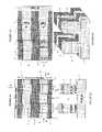
- FIGS. 1A , 2 A, 3 A, 4 A, 5 A, 6 A, 7 A, 8 A, 9 A, 10 A, 11 A, 12 A, 13 A, 14 A and 15 Aare top views of steps of making a device according to the first embodiment of the invention.
- FIGS. 1B , 2 B, 3 B, 4 B, 5 B, 6 B, 6 C, 7 B, 7 C, 8 B, 8 C, 9 B, 9 C, 10 B, 10 C, 11 B, 11 C, 12 B, 12 C, 13 B, 13 C, 14 B, 14 C, 15 B and 15 Care side cross sectional views of steps of making a device according to the first embodiment of the invention.
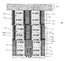
- FIG. 6Dis a three dimensional view of an in-process device shown in FIG. 6A .
- FIG. 16illustrates a side cross sectional view along the bit line direction of a completed vertical NAND string of the first embodiment of the invention.
- FIGS. 17A and 17Billustrate side cross sectional views of portions of the access transistor of NAND string according to second and third embodiments of the invention.
- FIGS. 18A and 19illustrate a circuit schematics of the NAND string of the embodiments of the invention.
- FIG. 18Billustrates a portion of the circuit schematic of FIG. 18A , but with the source lines, select lines and word lines removed for clarity.
- the embodiments of the inventionprovide a monolithic, three dimensional array of memory devices, such as an array of vertical NAND strings.
- the NAND stringsare vertically oriented, such that at least one memory cell is located over another memory cell.
- the arrayallows vertical scaling of NAND devices to provide a higher density of memory cells per unit area of silicon or other semiconductor material.
- This nonvolatile memorypreferably contains two charge trapping memory cells, such as SONOS cells, per 4F 2 in each memory level. Therefore, a four memory cell level configuration will have 0.5F 2 area per cell or 0.5F 2 binary bits per cell.
- the arraymay have two or more memory cell levels, such as two to eight levels. Thus, an N memory cell level configuration will have 4F 2 /2N area per cell.
- the select transistors for each NAND stringsmay also be monolithically integrated into each NAND string above and/or below the memory cells.
- a monolithic three dimensional memory arrayis one in which multiple memory levels are formed above a single substrate, such as a semiconductor wafer, with no intervening substrates.
- the term “monolithic”means that layers of each level of the array are directly deposited on the layers of each underlying level of the array.
- two dimensional arraysmay be formed separately and then packaged together to form a non-monolithic memory device.
- non-monolithic stacked memorieshave been constructed by forming memory levels on separate substrates and adhering the memory levels atop each other, as in Leedy, U.S. Pat. No. 5,915,167, titled “Three Dimensional Structure Memory.” The substrates may be thinned or removed from the memory levels before bonding, but as the memory levels are initially formed over separate substrates, such memories are not true monolithic three dimensional memory arrays.
- the preferred programming and erase method of the NAND stringis via Fowler-Nordheim (“FN”) tunneling.
- Multilevel cell (“MLC”) operation of the NAND string of the multiple VT states type or of the Saifon/mirror bit typeis also possible.
- the arraycontains two bits per 4F 2 in each memory level and provides further scaling by vertically integrating multiple memory levels.
- Each charge trapping memory cellcan be operated in a binary fashion providing large margins and high performance.
- select transistorscan also be vertically integrated and one or possibly both select transistors may be completely omitted.
- the vertical integration of select transistorseliminates any break in regular line and space patterning of masks used for each device level. There is no break in the continuity of regular and completely periodic lines and spaces within the entire memory array, allowing for small device features with a narrow pitch formed by lithography. In contrast to prior art two dimensional planar NAND devices, no extra space needs to be created for end of NAND string lines and spaces.
- Alternative embodimentsinclude configurations with select gates formed in trenches in the silicon wafer or other substrate, configurations with no select gate (i.e., no select gate lines and no select transistors), configurations with only select gate drain, configurations with only select gate source, and configurations with both select gates.
- Orientation of the select gate lines with respect to the orientation of the source lines, bit lines and word linescan be varied in various configurations. Even non-right angle orientation of various lines with respect to one another is possible, as will be described below.
- source linesmay be replaced by a common source region extending in both dimensions of the plane of the substrate and providing higher current sinking capability at the expense of inability to select individual source line voltages.
- the orientation of the memory levels with respect to one anothercan be varied also. For example, each memory level can have word lines that are oriented in perpendicular directions to the level above and to the level below.
- FIGS. 1A and 1Billustrate a first step in the method of making a NAND string according to a first embodiment of the invention.
- FIG. 1Ais a top view and FIG. 1B is a side cross sectional view along line A-A in FIG. 1A which extends parallel to the word lines.
- FIG. 1Billustrates a p-type silicon substrate 1 containing an n-type silicon layer 3 adjacent to the surface. It should be noted that p-type and n-type regions may be reversed and that semiconductor materials other than silicon, such as gallium arsenide for example, may be used.
- the substrate 1 and layer 3preferably comprise single crystal silicon.
- Layer 3may be formed by a blanket ion implantation or by epitaxially growing an n-type layer on a p-type substrate.
- the active regions 5 in substrate 1 and layer 3are separated from each other by insulating isolation regions 7 .
- Any suitable isolation regions 7may be used, such as LOCOS silicon oxide or STI oxide filled trenches.
- the pn junction between substrate 1 and layer 3is located above the bottom of the isolation regions 7 , such as above the STI trench bottom, to be able to drive each active device's voltage independent of the other devices.
- the STI isolation regions 7may be formed by patterning and etching standard STI trenches, performing thermal or radical liner oxidation, depositing trench fill oxide, and planarizing the fill oxide to the top of the silicon layer 3 by any suitable planarization method, such as chemical-mechanical polishing (CMP).
- CMPchemical-mechanical polishing
- FIGS. 2A and 2Billustrate a second step in the method of making the NAND string.
- FIG. 2Ais a top view and FIG. 2B is a side cross sectional view along line A-A in FIG. 2A which extends parallel to the word lines.
- a silicon layer 9is epitaxially grown on the active regions 5 exposed between the isolation regions 7 .
- the active regions 5act as a seed for the epitaxial growth of layer 9 . Therefore, the grain boundaries 11 in layer 9 are formed over the isolation regions 7 , while essentially single crystal silicon regions in layer 9 are formed over the active regions 5 .
- Layer 9contains a p-type region 15 between n-type regions 13 and 17 .
- Layer 9may be doped in-situ during growth by changing the dopant concentrations in the precursor gases. This forms the npn structure 13 , 15 , 17 that will later define source/channel/drain regions of vertical sidewall MOS select transistors. Ion implantation or other forms of doping the various layers 13 - 17 are also possible but result in a more complex process flow.
- the n-type region 13electrically and physically contacts the n-type active regions 5 in layer 3 .
- FIGS. 3A and 3Billustrate a third step in the method of making the NAND string.
- FIG. 3Ais a top view and FIG. 3B is a side cross sectional view along line A-A in FIG. 3A which extends parallel to the word lines.
- the epitaxial layer 9is planarized by any suitable planarization method, such as CMP, to provide a planar upper surface.
- FIGS. 4A and 4Billustrate a fourth step in the method of making the NAND string.
- FIG. 4Ais a top view and FIG. 4B is a side cross sectional view along line A-A in FIG. 4A which extends parallel to the word lines.
- the epitaxial layer 9is patterned into strips 19 .
- striprefers to a body that has a length which is much greater than its thickness or its width and which extends in one direction along its length.
- the strips 19 in the first embodimentextend along the bit line direction, as will be explained in more detail below.
- the strips 19are formed by forming a mask over the layer 9 , such as a photolithographically patterned photoresist layer mask, and etching the unmasked portions of layer 9 .
- the patterning of the stripsis not necessarily self aligned to the active regions S below.
- the strips 19are not aligned to the active regions 5 , such that the strips 19 extend laterally past the active regions S and over the isolation regions 7 , as shown in FIG. 5B and/or such that a portion of the active regions 5 are exposed below the strips 19 , as shown in FIG. 5A .
- FIGS. 5A and 5Billustrate a fifth step in the method of making the NAND string.
- FIG. 5Ais a top view and
- FIG. 5Bis a side cross sectional view along line A-A in FIG. 4A which extends parallel to the word lines.
- an insulating layersuch as silicon oxide and/or another insulating layer 21 is deposited between the strips and planarized with the top surface of the strips 19 .
- the insulating layer 21may be planarized by CMP or other planarization methods, such as etch back.
- FIGS. 6A to 6Dillustrate a sixth step in the method of making the NAND string.
- FIG. 6Ais a top view and
- FIG. 6Bis a side cross sectional view along line A-A in FIG. 6A which extends parallel to the word lines.
- FIG. 6Cis a side cross sectional view along line B-B in FIG. 6A which extends parallel to the bit lines.
- FIG. 6Dis a three dimensional view of the in process device shown in FIGS. 6A-6C .
- the strips 19 and portions of the insulating layer 21 between the strips 19are patterned into strips 23 which extend parallel to the word line direction and perpendicular to strips 19 .
- the strips 23are formed by forming a mask over the strips 19 and insulating layer 21 , such as a photolithographically patterned photoresist layer mask, and etching the unmasked portions of strips 19 and layer 21 .
- the strips 23consist of semiconductor pillars 25 separated from adjacent pillars in the word line direction by the portions of the insulating layer 21 .
- Each pillar 25is separated from adjacent pillars in the bit line direction by the trenches 27 between pillars.
- Each pillar 25contains a p-type conductivity semiconductor region 15 located between n-type conductivity type semiconductor regions 13 , 17 in the vertical direction (i.e., region 15 is above region 13 and below region 17 with respect to substrate 1 ).
- each pillar 25has a square or rectangular cross section when viewed from the top, as shown in FIG. 6A .
- each pillar 25preferably has four vertical sides.
- FIGS. 7A to 7Cillustrate a seventh step in the method of making the NAND string.
- FIG. 7Ais a top view and
- FIG. 7Bis a side cross sectional view along line A-A in FIG. 7A which extends parallel to the word lines.
- FIG. 7Cis a side cross sectional view along line B-B in FIG. 7A which extends parallel to the bit lines.
- a gate insulating layer 29is formed in the trenches 27 between the pillars 25 and over the top surfaces of the pillars 25 .
- the gate insulating layer 29may comprise silicon oxide, silicon nitride or any other suitable gate insulating layer material. If desired, layer 29 may contain two or more sublayers having a different composition.
- a select gate layeris then deposited over the gate insulating layer 29 .
- One or more of any suitable gate electrode materialsmay be used for the select gate layer, such as polysilicon, silicide (titanium silicide, etc.), tungsten, aluminum or a combination of sublayers of these materials.
- the select gate layeris then planarized with the top of the gate insulating layer 29 by any suitable planarization method, such as CMP.
- the planarizationleaves the select gates 31 located in portions of the trenches 27 above the gate insulating layer 29 , as shown in FIG. 7C .
- FIGS. 8A to 8Cillustrate an eighth step in the method of making the NAND string.
- FIG. 8Ais a top view and
- FIG. 8Bis a side cross sectional view along line A-A in FIG. 8A which extends parallel to the word lines.
- FIG. 8Cis a side cross sectional view along line B-B in FIG. 8A which extends parallel to the bit lines.
- the select gates 31are partially etched back so that the top of the select gates are located below the tops of the pillars 25 .
- the gates 31may be etched back using a selective etch which etches the gate material selectively over the gate insulating layer 29 material.
- FIGS. 9A to 9Cillustrate a ninth step in the method of making the NAND string.
- FIG. 9Ais a top view and
- FIG. 9Bis a side cross sectional view along line A-A in FIG. 9A which extends parallel to the word lines.
- FIG. 9Cis a side cross sectional view along line B-B in FIG. 9A which extends parallel to the bit lines.
- An insulating cap layeris deposited over the recessed select gates 31 and over the gate insulating layer 29 .
- the cap layercomprises the same material as the gate insulating layer 29 , such as silicon oxide.
- the cap layeris then planarized, such as CMP planarized, to fill the trenches located above the select gates 31 and to form insulating caps 33 located above each select gate 31 .
- the cap 33electrically isolates the select gates from the NAND string memory cells that will be formed above.
- the portions of the gate insulating layer 29 located above the semiconductor pillars 25are also removed to expose the top region 17 of the pillars 25 .
- the select gates 31comprise portions of select gate lines which extend in the word line direction.
- the select gate linescomprise strip shaped lines located in trenches 27 (which were shown in FIG. 6A ).
- Each select gate 31acts as a gate electrode for two adjacent select transistors 35 to the left and right of the gate 31 in FIG. 7C .
- each select field effect transistor 35comprises the pillar 25 active region, in which region 15 acts as a channel and regions 13 and 17 as “source” and “drain” regions, a select gate 31 which acts as the gate electrode of the transistor, and the gate insulating layer 29 located between the select gate 31 and the pillar 25 . Since each pillar 25 is located between two different select gates 31 , the left and right side of each pillar 25 can be considered as a separate select transistor 35 for the same NAND string to be formed above the pillar 25 .
- FIGS. 10A to 10Cillustrate a tenth step in the method of making the NAND string.
- FIG. 10Ais a top view and
- FIG. 10Bis a side cross sectional view along line A-A in FIG. 10 A which extends parallel to the word lines.
- FIG. 10Cis a side cross sectional view along line B-B in FIG. 10A which extends parallel to the bit lines,
- FIGS. 10A-10Cillustrate the first step in the formation of the memory cells above the select transistors 35 .
- the silicon surface of the exposed pillars 25is preferably cleaned after the CMP step in FIG. 9C .
- the top surface of each silicon pillarmay be treated by thermal or radical oxidation (i.e., to form a silicon oxide layer on the top of the pillars) followed by a wet, gentle oxide etch in order to remove the oxide layer along with the damage incurred during CMP and/or dry etches, to prepare the silicon surface for the growth of next epitaxial layer. Such damage may impact quality of the subsequent epitaxial layer growth.
- the next epitaxial layer 109is grown on the completed select gate transistors 35 .
- the subsequent steps of forming the first NAND memory cellare similar to the method steps shown in FIGS. 2-9 , except that a charge storage region is formed instead of a gate insulating layer 29 .
- the silicon layer 109is epitxially grown on the pillar active regions 25 exposed between the isolation regions formed by insulating layers 21 , 29 and 33 .
- PECVDplasma assisted epitaxy
- the silicon layer 109may be grown at lower temperatures, such as at 700° C. and below, for example at around 650° C. While higher temperature growth processes may be used, the low temperature PECVD process allows the use of lower thermal budget metals and dielectrics (i.e., metals and dielectrics that cannot withstand temperatures above 700° C.) and provide for more controlled junction depths and channel lengths.
- the exposed box shape upper surface of pillar active regions 25act as a seed for the epitaxial growth of layer 109 . Therefore, the grain boundaries 111 in layer 109 are formed over the isolation regions, while essentially single crystal silicon regions in layer 109 are formed over the active regions 25 .
- the grain growth of layer 109mushrooms out from the seeds 25 below and forms grain boundaries 111 where the grains meet each other during the epitaxy process.
- the position of the grain boundaries 111will be where random grains meet and the grain boundaries 111 will generally not be as smooth and predictable as schematically illustrated in FIGS. 10A-10C .
- the grain boundariesare located in regions that will be etched away during subsequent steps. Thus, a high level of smoothness and predictability is not required.
- Layer 109contains a p-type region 115 located between n-type regions 113 and 117 in the vertical direction. Layer 109 may be doped in-situ during growth by changing the dopant concentrations in the precursor gases. This forms the npn structure 113 , 115 , 117 that will later define source/channel/drain regions of charge trapping MOS memory devices (i.e., the NAND memory cells). Ion implantation or other forms of doping the various layers 113 - 117 are also possible but result in a more complex process flow. The n-type regions 113 electrically and physically contact the n-type active regions 17 in pillar 25 .
- FIGS. 11A to 11Cillustrate an eleventh step in the method of making the NAND string.
- FIG. 11Ais a top view and
- FIG. 11Bis a side cross sectional view along line A-A in FIG. 11A which extends parallel to the word lines.
- FIG. 11Cis a side cross sectional view along line B-B in FIG. 11A which extends parallel to the bit lines.
- the epitaxial layer 109is planarized by any suitable planarization method, such as CMP, to provide a planar upper surface.
- FIGS. 12A to 12Cillustrate a twelfth step in the method of making the NAND string.
- FIG. 12Ais a top view and
- FIG. 12Bis a side cross sectional view along line A-A in FIG. 12A which extends parallel to the word lines.
- FIG. 12Cis a side cross sectional view along line B-B in FIG. 12A which extends parallel to the bit lines.
- the epitaxial layer 109is patterned into strips 119 .
- striprefers to a body that has a length which is much greater than its thickness or its width and which extends in one direction along its length.
- the strips 119 in the first embodimentextend along the bit line direction, as will be explained in more detail below.
- the strips 119are formed by forming a mask over the layer 109 , such as a photolithographically patterned photoresist layer mask, and etching the unmasked portions of layer 109 .
- the patterning of the stripsis not necessarily self aligned to the pillar active regions 25 below.
- the strips 119are not aligned to the active regions 25 , such that the strips 119 extend laterally past the active regions 25 and over the isolation regions formed by layers 21 , 29 and 33 which surround the pillars 25 , as shown in FIGS. 12B and 12C and/or such that a portion of the active regions 25 are exposed below the strips 119 , as shown in FIG. 12A .
- FIGS. 13A to 13Cillustrate a thirteenth step in the method of making the NAND string.
- FIG. 13Ais a top view and
- FIG. 13Bis a side cross sectional view along line A-A in FIG. 13A which extends parallel to the word lines.
- FIG. 13Cis a side cross sectional view along line B-B in FIG. 13A which extends parallel to the bit lines.
- an insulating layersuch as silicon oxide and/or another insulating layer 121 is deposited between the strips 119 adjacent to exposed lateral sides of the strips 119 .
- Layer 121is then planarized with the top surface of the strips 119 .
- the insulating layer 121may be planarized by CMP or other planarization methods, such as etch back.
- FIGS. 14A to 14Cillustrate a fourteenth step in the method of making the NAND string.
- FIG. 14Ais a top view and
- FIG. 14Bis a side cross sectional view along line A-A in FIG. 14A which extends parallel to the word lines.
- FIG. 14Cis a side cross sectional view along line B-B in FIG. 14A which extends parallel to the bit lines
- the strips 119 and portions of the insulating layer 121 between the strips 119are patterned into strips 123 which extend parallel to the word line direction and perpendicular to strips 119 .
- the strips 123are formed by forming a mask over the strips 119 and insulating layer 121 , such as a photolithographically patterned photoresist layer mask, and etching the unmasked portions of strips 119 and layer 121 .
- the strips 123consist of semiconductor pillars 125 separated from adjacent pillars in the word line direction by the portions of the insulating layer 121 .
- Each pillar 125is separated from adjacent pillars in the bit line direction by the trenches 127 between pillars.
- Each pillar 125contains a p-type conductivity semiconductor region 115 located between n-type conductivity type semiconductor regions 113 , 117 in the vertical direction (i.e., region 115 is above region 113 and below region 117 with respect to substrate 1 ).
- each pillar 125has a square or rectangular cross section when viewed from the top, as shown in FIG. 14A .
- each pillar 125preferably has four vertical sides.
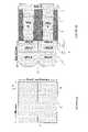
- FIGS. 15A to 15Cillustrate a fifteenth step in the method of making the NAND string.
- FIG. 15Ais a top view and
- FIG. 15Bis a side cross sectional view along line A-A in FIG. 15A which extends parallel to the word lines.
- FIG. 15Cis a side cross sectional view along line B-B in FIG. 15A which extends parallel to the bit lines.
- a charge storage regionis formed between the strips 123 .
- the charge storage regionmay comprise a dielectric isolated floating gate or a dielectric charge storage material.
- a dielectric isolated floating gatea polysilicon layer is deposited between two insulating layers, such as silicon oxide tunneling and blocking layers.
- sidewall spacer formed floating gatesmay be used. The additional space taken by spacer floating gate may be recouped by utilizing multilevel cell (MLC) programming for these devices.
- MLCmultilevel cell
- a charge storage dielectric layeris deposited between tunneling and blocking dielectric (i.e., insulating) layers.
- the charge storage dielectric layermay comprise a silicon nitride layer while the tunneling and blocking layers may comprise silicon oxide layers to form an “ONO” charge storage region of a “SONOS” type device.
- the tunneling dielectric layeris thinner than the blocking dielectric layer.
- high dielectric constant insulating materialssuch as materials having a dielectric constant of above 3.9, may be used for the tunneling and/or the blocking dielectric layer instead of silicon oxide.
- These materialsinclude metal oxide layers, such as aluminum oxide, tantalum oxide, yttrium oxide, calcium oxide, magnesium oxide or zirconium oxide.
- the charge storage dielectricmay alternatively comprise a silicon oxynitride layer in which a portion of nitrogen in the silicon nitride layer is substituted with oxygen.
- a metal oxide layersuch as tantalum oxide, zirconium oxide or hafnium oxide, may be used as the charge storage dielectric.
- ONO charge storage regionwill be described. However, it should be understood that a floating gate charge storage region or other dielectric charge storage material combinations may be used instead.
- a tunneling dielectric layer 128 , a charge storage dielectric layer 129 and a blocking dielectric layer 130are formed in that order in the trenches 127 between the pillars 125 (i.e., adjacent to exposed sides of the pillars) and over the top surfaces of the pillars 125 .
- the tunneling and blocking dielectricsmay comprise silicon oxide while the charge storage dielectric may comprise silicon nitride.
- a control gate layeris then deposited over the dielectric layers 128 - 130 .
- One or more of any suitable gate electrode materialsmay be used for the control gate layer, such as polysilicon, silicide (titanium silicide, etc.), tungsten, aluminum or a combination of sublayers of these materials.
- control gate layeris then planarized with the top of the tunneling layer 128 by any suitable planarization method, such as CMP.
- CMPplanarization method
- the control gates 131are partially etched back so that the top of the gates are located below the tops of the pillars 125 .
- the gates 131may be etched back using a selective etch which etches the gate material selectively over the ONO dielectric layers 128 - 130 .
- An insulating cap layeris then deposited over the recessed control gates 131 and over the ONO dielectrics.
- the cap layercomprises the same material as the blocking dielectric 130 , such as silicon oxide.
- the cap layeris then planarized, such as CMP planarized, to fill the trenches located above the control gates 131 and to form insulating caps 133 located above each control gate 131 .
- the cap 133electrically isolates the control gates from additional NAND string memory cells that will be formed above.
- the portions of the ONO dielectric layers 128 - 130 located above the semiconductor pillars 125are also removed to expose the top region 117 of the pillars 125 .
- control gates 131comprise portions of word lines which extend below the caps 133 in the word line direction.
- the word gate linescomprise strip shaped lines located in trenches 127 .
- Each control gate 131acts as a gate electrode for two adjacent memory cells 135 to the left and right of the gate 131 in FIG. 15C .
- Each memory cell 135comprises the pillar 125 active region, in which region 115 acts as a channel and regions 113 and 117 as “source” and “drain” regions, a control gate/word line 131 which acts as the gate electrode of the transistor, and the charge storage region, such as the ONO dielectric layers 128 - 130 located between the control gate 131 and the pillar 125 . Since each pillar 125 is located between two different control gates 131 , the left and right side of each pillar 125 can be considered as a memory cell.
- FIG. 16illustrates a side cross sectional view along the bit line direction of a completed vertical NAND string.
- a second level of memory cells 235which are identical to the first memory cells 135 is formed on the first memory cells 135 by repeating the process steps described above with respect to FIGS. 10-15 to form a multilevel vertical NAND string. If desired, additional levels of memory cells, such as two to six levels of memory cells may be formed over the first level of memory cells 135 by repeating the process steps described above.
- a plurality of bit lines 137are then formed above the upper most level of memory cells. The bit lines 137 contacts the pillar active regions of the upper level of memory cells. For example, the single bit line 137 shown in FIG. 16 extends perpendicular to the word lines 131 , 231 of the memory cells. However, the bit lines 137 may extend in other directions as will be described in more detail below.
- an upper select transistormay be above the upper level of the memory cells below the bit lines 137 using the same method as the lower select gate transistor 35 .
- the upper select gate transistoris formed in addition to or instead of the lower select gate transistor 35 .
- FIG. 16illustrates the vertical NAND string 100 which is formed vertically over the substrate.
- One memory cell 235is located in an upper device level and another memory cell 135 is located in a lower device level located over the substrate and below the first device level 235 .
- active regions 125 and 225are grown in different epitaxial growth steps, a defined boundary exists between the semiconductor active regions 125 and 225 .
- the boundarymay comprise a dislocation, a grain boundary or a lateral offset of the pillar 225 with respect to pillar 125 at the boundary.
- the pillar shaped active regions of the vertical NAND string memory cells made by the method described abovehave a square or rectangular cross section when it is viewed from the top. This provides separate faces for each word line in each cell and allows the two bit per cell configuration.
- the pillar shaped active regionsare formed by patterning the active layer into strips and then patterning the strips into pillars.
- the active regions of Endoh et al.have a circular cross section when viewed from the top. The active regions are surrounded by a surround gate for a one bit per cell configuration.
- the semiconductor active region 25 of the select transistor 35comprises a pillar.
- the semiconductor active region 125 of the lower memory cellcomprises a pillar which is not aligned with the semiconductor active region 25 of the select transistor 35 .
- the active region 125extends laterally in at least one direction past the semiconductor active region 25 of the select transistor 35 .
- the pillar active region 225extends laterally in at least one direction past the pillar active region 125 of cell 135 , such that the pillar 125 is not aligned with the pillar 225 .
- the semiconductor active region of the memory cell 135is a pillar 125 comprising a first conductivity type semiconductor region 115 located between second conductivity type semiconductor regions 113 , 117 .
- the semiconductor active region of memory cell 235is a pillar 225 comprising a first conductivity type semiconductor region 215 located between second conductivity type semiconductor regions 213 , 217 .
- the second conductivity type semiconductor region 213 in pillar 225contacts second conductivity type semiconductor region 117 in pillar 125 .
- a first charge storage dielectric 129 Ais located adjacent to one side of the first conductivity type semiconductor region 115 in the pillar 125 and a first control gate 131 A is located adjacent to the first charge storage dielectric 129 A.
- a second charge storage dielectric 129 Bis located adjacent to the opposite side of first conductivity type semiconductor region 115 in the pillar 125 , and a second control gate 131 B is located adjacent to the second charge storage dielectric 129 B.
- a similar configurationis present in the upper memory cell 235 , where the two charge storage dielectrics and two control gates are located on opposite sides of region 215 in pillar 225 .
- FIGS. 17A and 17Billustrate side cross sectional views of portions of the select transistor of NAND string according to alternative second and third embodiments of the invention.
- FIG. 17Aa side cross sectional view along the word line direction of the second embodiment in which the lower select transistor 35 is omitted.
- the bottom memory cell levelis formed over the substrate 1 .
- FIG. 17Ba side cross sectional view along the bit line direction of the third embodiment in which the select gates 31 of the select transistors 35 are formed in trenches in the substrate 1 .
- a p-type substrate 1contains an n-p-n structure 13 , 15 , 17 formed by ion implantation of n-type ions into the substrate 1 to leave a p-type regions of the substrate 15 between the implanted n-type regions 13 and 17 .
- regions 13 - 17may be formed by epitaxial layer growth and in-situ doping during growth.
- trenchesare formed by photolithography and etching through the npn structure to the p-type portions of the substrate 1 .
- the trenchesare filled with an insulating material 20 , such as silicon oxide.
- the insulating material 20is then patterned by photolithography and etching to form additional trenches in the material 20 .
- These additional trenchesare filled with the select gate material which is then planarized to form the select gates 31 . If the select transistor 35 is omitted, then the lowest memory cell 135 may be formed in the trench instead.
- the pillar active regions 25 , 125 , etc. of the select transistors and/or of the memory cellsare formed in polycrystalline semiconductor material 9 , 109 , etc.
- an amorphous, microcrystalline or polycrystalline semiconductor layersuch as a silicon layer, is formed on the underlying pillars. This amorphous, microcrystalline or polycrystalline semiconductor layer is then recrystallized to form a large grain polycrystalline semiconductor material layer, such as a large grain polysilicon layer.
- the recrystallizationmay be conducted by any suitable annealing method, such as thermal annealing in a furnace, laser annealing and/or flash lamp annealing. This recrystallized layer is then patterned into pillar active regions 25 , 125 , etc., as described above.
- annealing methodsuch as thermal annealing in a furnace, laser annealing and/or flash lamp annealing.
- This recrystallized layeris then patterned into pillar active regions 25 , 125 , etc., as described above.
- the use of low temperature deposited and recrystallized polysiliconallows the active regions to be formed over metal wiring or electrodes which cannot withstand high temperatures.
- the semiconductor active region of an upper memory cellcan be formed epitaxially on a semiconductor active region of the underlying memory cell or the semiconductor active regions of one or more first memory cells may be formed in recrystallized polysilicon.
- the active regions of the lowest level of the memory cellsis formed epitaxially or by recrystallization on a semiconductor active region of the select transistor.
- the active regions of the select transistorsare formed epitaxially or by recrystallization over the substrate.
- the memory array's size in the lateral dimensionsis limited by the RC time constants of the word lines, select gate lines, source lines, and the bit lines.
- the NAND stringsare oriented vertically, and the channel regions (P-regions 115 the NMOS memory embodiment shown) are not grounded. Thus, care has to be taken to manage this floating body potential.
- the inversion layer on the opposite (non-selected) sidecan be created and utilized to help anchor the potential of the floating P-type bodies during various operations such as read, program, and/or erase.
- Highly doped N and P regions with abrupt junctionsmay also be used such that floating bodies can be more strongly coupled to one another through thinner depletion regions. Another way of dictating the floating body potentials is through their junction leakages.
- boosting for program inhibitshould be much more efficient.
- the silicon pillar active regionscan be driven as opposed to being boosted, allowing for more abrupt junctions.
- each memory cell and select transistor levelis completely self aligned to itself. In other words, no separate alignment steps between device levels is required. Furthermore, each device level only requires two lithography steps—the first step to form the first strips 119 and the second step to form strips 123 . The remaining features in each device level are formed by layer deposition and planarization. Thus, at least one region or layer of the NAND string 100 , and preferably plural regions or layers are planarized by CMP and/or other methods. For example, for cell 135 the semiconductor active region 125 is planarized when it is in the form of epitaxial layer 109 , as shown in FIGS.
- the insulating layer 121 which insulates the NAND string 100 from at least one other adjacent NAND stringis planarized as shown in FIG. 13B
- the charge storage dielectric 129 , the control gate 131 and the cap layer 133are planarized as shown in FIGS. 15B and 15C .
- at least five layersare planarized by CMP in each cell 135 , 235 , etc.
- the silicon wafer substrate 1may be rotated 45° during all lithography steps so that the wafer notch is not at the 12 o'clock position but at the 1:30 position. In this case, then the vertical side wall channels will be on a [100] crystallographic plane, providing higher channel mobility.
- Each device levelis not self aligned to the level below it. However, this is of little consequence because the regions where the levels meet is intentionally designed to be the inactive source/drain regions of the NAND chain.
- the vertical dimensions of each level and the positions of the PN junctions in each levelcan be different from the other levels based on thermal budgets related to annealing of various levels.
- Low temperature (such as a temperature below 700° C.) semiconductor epitaxial growth, such as PECVD growth, and plasma oxidationmay be employed to minimize level to level variation. This also allows a single high temperature anneal after the forming of all memory and select gate levels. However, separate level by level annealing, or multiple anneal steps for each memory/select level may also be used. If desired, an anneal in a hydrogen ambient may also be conducted.
- the pillarsare preferably rectangular or square when viewed from the side.
- the active layerssuch as the select transistor pillar active region portions 5 , will be in the form of truncated pyramids with larger rectangular or square bases than tops. Thus, certain amount of misalignment will not result in variation in contact areas of top of one silicon pillar to the bottom of silicon pillar of the layer above it.
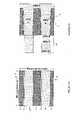
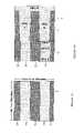
- FIG. 18Aillustrates a circuit schematic of an array of NAND strings described above.
- FIG. 18Billustrates a portion of the circuit schematic of FIG. 18A , but with the source lines, select lines and word lines removed for clarity.
- FIGS. 18A and 18Billustrate the select transistors 35 , located on a substrate or in a trench in the substrate and at least two levels of memory cells located vertically over the select transistors 35 .
- Each NAND stringis depicted as a single column, in which each level of memory cells is located over the underlying level of memory cells.
- the middle vertical NAND string 100 controlled by bit line 237 in column Mincludes the select transistor 35 and four memory cells 135 , 235 , 345 and 445 in four levels.
- the select transistor 35is connected to source line SL in row N+1 ⁇ 2.
- the select transistor 35is controlled by select gate lines 31 in rows N and N+1.
- the lowest memory cell 135is controlled by word lines 131 in rows N and N+1 in vertical level 1 (shown in FIG. 18A as WL (N+X row, Z level), such as WL (N, 1) for word line in row N, level 1).
- the other memory cells 235 , 335 and 445are controlled by word lines 231 , 331 and 441 in rows N and N+1 in levels 2, 3 and 4, respectively.
- the upper memory cell 445is electrically connected to the bit line 237 in bit line column M.
- each vertical NAND stringincludes the select transistor 35 and vertically arranged memory cells 135 - 445 located one over another.
- the word lines 131 to 431are not parallel to the bit line 237 .
- the word linesextend perpendicular to the bit line 237 .
- the word lines 131 - 431extend parallel to at least one of the source line 239 and the select gate line 31 , such as parallel to both the source line 239 and the select gate line 31 .
- the word lines in different vertical levelscan extend in different directions from each other.
- the word lines 131 in memory cell level onemay extend in a different direction, such as in a perpendicular direction, from the word lines 231 in memory cell level two.
- the word line directionmay be alternated between each memory cell level.
- the word lines in levels one and threemay extend in one direction and the word lines in levels two and four may extend in a different direction.
- the word line directionsmay differ by one to ninety degrees from each other.
- This configurationmay reduce coupling between device levels by placing charge storage locations adjacent to different faces of the pillar active regions in adjacent memory cell levels (for example the charge is stored adjacent to north and south faces of the pillar in levels one and three and adjacent to east and west faces in levels two and four).
- bit lines, the word lines and the source linesare not parallel to each other.
- the bit lines 237are not parallel to the word lines 131 - 431 which are not parallel to the source lines 239 which are not parallel to the bit lines.
- the word lines 131 - 431may extend perpendicular to the source lines 239
- the bit lines 237extend diagonally (i.e., at an angle of 1 to 89 degrees, such as 30 to 60 degrees, for example 45 degrees) with respect to the word lines and the source lines.
- the current from each bit linesinks to an individually selected source line, thus decreasing the amount of current provided to a particular source line.
- the diagonal bit lines of FIG. 19may have a narrower pitch than the bit lines shown in FIGS. 18A and 18B .
- the arrangementmay be varied such that the word and bit lines are perpendicular to each other and the source lines are diagonal.
- the source linesmay be formed on top and the bit lines may be formed on the bottom. This allows formation of metal and/or silicide rather than semiconductor source lines, which leads to a decreased current crowding due to the lower resistivity source line material.
- all three types of linesmay be non-perpendicular to each other and extend diagonally with respect to each other.
- the select linesare parallel to the word lines.
- each memory cellhas a different associated word line, bit line and source line combination that all other memory cells in the array.
- all memory cells in one row parallel to the word line directionare controlled by different bit lines and different source lines.
- the configuration of FIG. 19allows each memory cell in the array to be individually programmed (instead of programming each adjacent pair of cells together) even when two adjacent cells share the same word line, because these adjacent cells are connected to a different combination of bit lines and source lines from each other.
- two adjacent cells in the same column parallel to one source lineare controlled by a different bit line.
- two adjacent cells in the same columnare associated with the same word line and source line but a different bit line.
- the select transistors 31may optionally be omitted in the configuration of FIG. 19 due to the ability to program each memory cell individually using bit line by bit line control for programming of the cells.
- the progranirnngpreferably takes place level by level in each NAND string 200 , with alternating levels being programmed sequentially.
- the source lines 239are be replaced by a common source region (source plane) extending in both dimensions of the plane of the substrate 1 (i.e., in the x-y plane).
- the common source regionmay comprise a common conductive plate, such as a highly doped single crystal or polycrystalline semiconductor, silicide and/or metal plate, which electrically contacts the pillar active regions 25 of all select transistors 35 of the array. If the select transistors are omitted, then the source plate contacts the pillars 125 of the lowest memory cell 135 level.
- the common source plateprovides a higher current sinking capability at the expense of loosing the ability to select individual source line voltages.
- An alternative embodiment for MLC operationhas both source lines and bit lines extending along the same direction to provide means to vary the entire NAND chain voltage on a bit line by bit line basis in order to program cells that are being programmed to higher V T states faster than cells that are being programmed to lower V T states.
- the source and bit line voltages of cells that are being programmed to lower V T stateswill be raised in order to retard programming of some these cells, so that the entire set of states in a two or three dimensional configurations will be programmed using fewer program pulses.
Landscapes
- Semiconductor Memories (AREA)
- Non-Volatile Memory (AREA)
Abstract
Description
- This application is related to Mokhlesi et al., U.S. application Ser. No. __/______, titled “THREE DIMENSIONAL NAND MEMORY” (Attorney Docket No. 035905/0145), Mokhlesi et al., U.S. application Ser. No. __/______, titled “METHOD OF MAKING THREE DIMENSIONAL NAND MEMORY” (Attorney Docket No. 035905/0146), Mokhlesi et al., U.S. application Ser. No. __/______, titled “METHOD OF MAKING THREE DIMENSIONAL NAND MEMORY” (Attorney Docket No. 035905/0148), Mokhlesi et al., U.S. application Ser. No. __/______, titled “THREE DIMENSIONAL NAND MEMORY” (Attorney Docket No. 035905/0149), and Mokhlesi et al., U.S. application Ser. No. __/______, titled “METHOD OF MAKING THREE DIMENSIONAL NAND MEMORY” (Attorney Docket No. 035905/0150), each filed on the same day herewith, and each hereby incorporated by reference in its entirety.
- The present invention relates generally to the field of semiconductor devices and specifically to three dimensional NAND strings and other three dimensional devices.
- Three dimensional vertical NAND strings are disclosed in an article by T. Endoh, et. al., titled “Novel Ultra High Density Memory With A Stacked-Surrounding Gate Transistor (S-SGT) Structured Cell”, IEDM Proc. (2001) 33-36. However, this NAND string provides only one bit per cell. Furthermore, the active regions of the NAND string is formed by a relatively difficult and time consuming process involving repeated formation of sidewall spacers and etching of a portion of the substrate, which results in a roughly conical active region shape.
- According to one embodiment of the invention a monolithic, three dimensional NAND string comprises a first memory cell located over a second memory cell, a select transistor, a first word line of the first memory cell, a second word line of the second memory cell, a bit line, a source line, and a select gate line of the select transistor. The first and the second word lines are not parallel to the bit line, and the first and the second word lines extend parallel to at least one of the source line and the select gate line.
- According to another embodiment of the invention a monolithic, three dimensional NAND string comprises a first memory cell located over a second memory cell, a first word line of the first memory cell, and a second word line of the second memory cell. The first word line extends in first direction, and the second word line extends in a second direction different from the first direction.
- According to another embodiment of the invention a NAND array comprises an array of vertical NAND strings, a plurality of word lines, a plurality of bit lines, and a plurality of source lines. The bit lines are not parallel to the word lines, the word lines are not parallel to the source lines, and the source lines are not parallel to the bit lines.
FIGS. 1A ,2A,3A,4A,5A,6A,7A,8A,9A,10A,11A,12A,13A,14A and15A are top views of steps of making a device according to the first embodiment of the invention.FIGS. 1B ,2B,3B,4B,5B,6B,6C,7B,7C,8B,8C,9B,9C,10B,10C,11B,11C,12B,12C,13B,13C,14B,14C,15B and15C are side cross sectional views of steps of making a device according to the first embodiment of the invention.FIG. 6D is a three dimensional view of an in-process device shown inFIG. 6A .FIG. 16 illustrates a side cross sectional view along the bit line direction of a completed vertical NAND string of the first embodiment of the invention.FIGS. 17A and 17B illustrate side cross sectional views of portions of the access transistor of NAND string according to second and third embodiments of the invention.FIGS. 18A and 19 illustrate a circuit schematics of the NAND string of the embodiments of the invention.FIG. 18B illustrates a portion of the circuit schematic ofFIG. 18A , but with the source lines, select lines and word lines removed for clarity.- Embodiments of the present invention will be described below with reference to the accompanying drawings. It should be understood that the following description is intended to describe exemplary embodiments of the invention, and not to limit the invention.
- The embodiments of the invention provide a monolithic, three dimensional array of memory devices, such as an array of vertical NAND strings. The NAND strings are vertically oriented, such that at least one memory cell is located over another memory cell. The array allows vertical scaling of NAND devices to provide a higher density of memory cells per unit area of silicon or other semiconductor material. This nonvolatile memory preferably contains two charge trapping memory cells, such as SONOS cells, per 4F2in each memory level. Therefore, a four memory cell level configuration will have 0.5F2area per cell or 0.5F2binary bits per cell. The array may have two or more memory cell levels, such as two to eight levels. Thus, an N memory cell level configuration will have 4F2/2N area per cell. If desired, the select transistors for each NAND strings may also be monolithically integrated into each NAND string above and/or below the memory cells.
- A monolithic three dimensional memory array is one in which multiple memory levels are formed above a single substrate, such as a semiconductor wafer, with no intervening substrates. The term “monolithic” means that layers of each level of the array are directly deposited on the layers of each underlying level of the array. In contrast, two dimensional arrays may be formed separately and then packaged together to form a non-monolithic memory device. For example, non-monolithic stacked memories have been constructed by forming memory levels on separate substrates and adhering the memory levels atop each other, as in Leedy, U.S. Pat. No. 5,915,167, titled “Three Dimensional Structure Memory.” The substrates may be thinned or removed from the memory levels before bonding, but as the memory levels are initially formed over separate substrates, such memories are not true monolithic three dimensional memory arrays.
- The preferred programming and erase method of the NAND string is via Fowler-Nordheim (“FN”) tunneling. Multilevel cell (“MLC”) operation of the NAND string of the multiple VT states type or of the Saifon/mirror bit type is also possible.
- Thus, the array contains two bits per 4F2in each memory level and provides further scaling by vertically integrating multiple memory levels. Each charge trapping memory cell can be operated in a binary fashion providing large margins and high performance. Further efficiencies are provided by the fact that select transistors can also be vertically integrated and one or possibly both select transistors may be completely omitted. The vertical integration of select transistors eliminates any break in regular line and space patterning of masks used for each device level. There is no break in the continuity of regular and completely periodic lines and spaces within the entire memory array, allowing for small device features with a narrow pitch formed by lithography. In contrast to prior art two dimensional planar NAND devices, no extra space needs to be created for end of NAND string lines and spaces.
- Alternative embodiments include configurations with select gates formed in trenches in the silicon wafer or other substrate, configurations with no select gate (i.e., no select gate lines and no select transistors), configurations with only select gate drain, configurations with only select gate source, and configurations with both select gates. Orientation of the select gate lines with respect to the orientation of the source lines, bit lines and word lines can be varied in various configurations. Even non-right angle orientation of various lines with respect to one another is possible, as will be described below. In some embodiments, source lines may be replaced by a common source region extending in both dimensions of the plane of the substrate and providing higher current sinking capability at the expense of inability to select individual source line voltages. The orientation of the memory levels with respect to one another can be varied also. For example, each memory level can have word lines that are oriented in perpendicular directions to the level above and to the level below.
FIGS. 1A and 1B illustrate a first step in the method of making a NAND string according to a first embodiment of the invention.FIG. 1A is a top view andFIG. 1B is a side cross sectional view along line A-A inFIG. 1A which extends parallel to the word lines.FIG. 1B illustrates a p-type silicon substrate 1 containing an n-type silicon layer 3 adjacent to the surface. It should be noted that p-type and n-type regions may be reversed and that semiconductor materials other than silicon, such as gallium arsenide for example, may be used. Thesubstrate 1 andlayer 3 preferably comprise single crystal silicon.Layer 3 may be formed by a blanket ion implantation or by epitaxially growing an n-type layer on a p-type substrate. Theactive regions 5 insubstrate 1 andlayer 3 are separated from each other by insulatingisolation regions 7. Anysuitable isolation regions 7 may be used, such as LOCOS silicon oxide or STI oxide filled trenches. Preferably, the pn junction betweensubstrate 1 andlayer 3 is located above the bottom of theisolation regions 7, such as above the STI trench bottom, to be able to drive each active device's voltage independent of the other devices. TheSTI isolation regions 7 may be formed by patterning and etching standard STI trenches, performing thermal or radical liner oxidation, depositing trench fill oxide, and planarizing the fill oxide to the top of thesilicon layer 3 by any suitable planarization method, such as chemical-mechanical polishing (CMP).FIGS. 2A and 2B illustrate a second step in the method of making the NAND string.FIG. 2A is a top view andFIG. 2B is a side cross sectional view along line A-A inFIG. 2A which extends parallel to the word lines. As shown inFIG. 2B , asilicon layer 9 is epitaxially grown on theactive regions 5 exposed between theisolation regions 7. Theactive regions 5 act as a seed for the epitaxial growth oflayer 9. Therefore, thegrain boundaries 11 inlayer 9 are formed over theisolation regions 7, while essentially single crystal silicon regions inlayer 9 are formed over theactive regions 5.Layer 9 contains a p-type region 15 between n-type regions Layer 9 may be doped in-situ during growth by changing the dopant concentrations in the precursor gases. This forms thenpn structure type region 13 electrically and physically contacts the n-typeactive regions 5 inlayer 3.FIGS. 3A and 3B illustrate a third step in the method of making the NAND string.FIG. 3A is a top view andFIG. 3B is a side cross sectional view along line A-A inFIG. 3A which extends parallel to the word lines. As shown inFIG. 3B , theepitaxial layer 9 is planarized by any suitable planarization method, such as CMP, to provide a planar upper surface.FIGS. 4A and 4B illustrate a fourth step in the method of making the NAND string.FIG. 4A is a top view andFIG. 4B is a side cross sectional view along line A-A inFIG. 4A which extends parallel to the word lines. Theepitaxial layer 9 is patterned into strips19. As used herein, the term “strip” refers to a body that has a length which is much greater than its thickness or its width and which extends in one direction along its length. Thestrips 19 in the first embodiment extend along the bit line direction, as will be explained in more detail below.- The
strips 19 are formed by forming a mask over thelayer 9, such as a photolithographically patterned photoresist layer mask, and etching the unmasked portions oflayer 9. As shown inFIGS. 5A and 5B , the patterning of the strips is not necessarily self aligned to the active regions S below. Preferably, but not necessarily, thestrips 19 are not aligned to theactive regions 5, such that thestrips 19 extend laterally past the active regions S and over theisolation regions 7, as shown inFIG. 5B and/or such that a portion of theactive regions 5 are exposed below thestrips 19, as shown inFIG. 5A . FIGS. 5A and 5B illustrate a fifth step in the method of making the NAND string.FIG. 5A is a top view andFIG. 5B is a side cross sectional view along line A-A inFIG. 4A which extends parallel to the word lines.- As shown in
FIGS. 5A and 5B , an insulating layer, such as silicon oxide and/or another insulatinglayer 21 is deposited between the strips and planarized with the top surface of thestrips 19. The insulatinglayer 21 may be planarized by CMP or other planarization methods, such as etch back. FIGS. 6A to 6D illustrate a sixth step in the method of making the NAND string.FIG. 6A is a top view andFIG. 6B is a side cross sectional view along line A-A inFIG. 6A which extends parallel to the word lines.FIG. 6C is a side cross sectional view along line B-B inFIG. 6A which extends parallel to the bit lines.FIG. 6D is a three dimensional view of the in process device shown inFIGS. 6A-6C .- The
strips 19 and portions of the insulatinglayer 21 between thestrips 19 are patterned intostrips 23 which extend parallel to the word line direction and perpendicular to strips19. Thestrips 23 are formed by forming a mask over thestrips 19 and insulatinglayer 21, such as a photolithographically patterned photoresist layer mask, and etching the unmasked portions ofstrips 19 andlayer 21. - The
strips 23 consist ofsemiconductor pillars 25 separated from adjacent pillars in the word line direction by the portions of the insulatinglayer 21. Eachpillar 25 is separated from adjacent pillars in the bit line direction by thetrenches 27 between pillars. Eachpillar 25 contains a p-typeconductivity semiconductor region 15 located between n-type conductivitytype semiconductor regions region 15 is aboveregion 13 and belowregion 17 with respect to substrate1). - Preferably, each
pillar 25 has a square or rectangular cross section when viewed from the top, as shown inFIG. 6A . Thus, eachpillar 25 preferably has four vertical sides. FIGS. 7A to 7C illustrate a seventh step in the method of making the NAND string.FIG. 7A is a top view andFIG. 7B is a side cross sectional view along line A-A inFIG. 7A which extends parallel to the word lines.FIG. 7C is a side cross sectional view along line B-B inFIG. 7A which extends parallel to the bit lines.- As shown in
FIG. 7C , agate insulating layer 29 is formed in thetrenches 27 between thepillars 25 and over the top surfaces of thepillars 25. Thegate insulating layer 29 may comprise silicon oxide, silicon nitride or any other suitable gate insulating layer material. If desired,layer 29 may contain two or more sublayers having a different composition. - A select gate layer is then deposited over the
gate insulating layer 29. One or more of any suitable gate electrode materials may be used for the select gate layer, such as polysilicon, silicide (titanium silicide, etc.), tungsten, aluminum or a combination of sublayers of these materials. - The select gate layer is then planarized with the top of the
gate insulating layer 29 by any suitable planarization method, such as CMP. The planarization leaves theselect gates 31 located in portions of thetrenches 27 above thegate insulating layer 29, as shown inFIG. 7C . FIGS. 8A to 8C illustrate an eighth step in the method of making the NAND string.FIG. 8A is a top view andFIG. 8B is a side cross sectional view along line A-A inFIG. 8A which extends parallel to the word lines.FIG. 8C is a side cross sectional view along line B-B inFIG. 8A which extends parallel to the bit lines.- As shown in
FIG. 8C , theselect gates 31 are partially etched back so that the top of the select gates are located below the tops of thepillars 25. Thegates 31 may be etched back using a selective etch which etches the gate material selectively over thegate insulating layer 29 material. FIGS. 9A to 9C illustrate a ninth step in the method of making the NAND string.FIG. 9A is a top view andFIG. 9B is a side cross sectional view along line A-A inFIG. 9A which extends parallel to the word lines.FIG. 9C is a side cross sectional view along line B-B inFIG. 9A which extends parallel to the bit lines.- An insulating cap layer is deposited over the recessed
select gates 31 and over thegate insulating layer 29. Preferably, the cap layer comprises the same material as thegate insulating layer 29, such as silicon oxide. The cap layer is then planarized, such as CMP planarized, to fill the trenches located above theselect gates 31 and to form insulatingcaps 33 located above eachselect gate 31. Thecap 33 electrically isolates the select gates from the NAND string memory cells that will be formed above. During the planarization of the cap layer, the portions of thegate insulating layer 29 located above thesemiconductor pillars 25 are also removed to expose thetop region 17 of thepillars 25. - As shown in
FIG. 9A , theselect gates 31 comprise portions of select gate lines which extend in the word line direction. Thus, the select gate lines comprise strip shaped lines located in trenches27 (which were shown inFIG. 6A ). Eachselect gate 31 acts as a gate electrode for two adjacentselect transistors 35 to the left and right of thegate 31 inFIG. 7C . - Thus, the ninth step completes the bottom
select transistor 35 for the NAND string. Each selectfield effect transistor 35 comprises thepillar 25 active region, in whichregion 15 acts as a channel andregions select gate 31 which acts as the gate electrode of the transistor, and thegate insulating layer 29 located between theselect gate 31 and thepillar 25. Since eachpillar 25 is located between two differentselect gates 31, the left and right side of eachpillar 25 can be considered as a separateselect transistor 35 for the same NAND string to be formed above thepillar 25. FIGS. 10A to 10C illustrate a tenth step in the method of making the NAND string.FIG. 10A is a top view andFIG. 10B is a side cross sectional view along line A-A in FIG.10A which extends parallel to the word lines.FIG. 10C is a side cross sectional view along line B-B inFIG. 10A which extends parallel to the bit lines,FIGS. 10A-10C illustrate the first step in the formation of the memory cells above theselect transistors 35. First, the silicon surface of the exposedpillars 25 is preferably cleaned after the CMP step inFIG. 9C . For example, the top surface of each silicon pillar may be treated by thermal or radical oxidation (i.e., to form a silicon oxide layer on the top of the pillars) followed by a wet, gentle oxide etch in order to remove the oxide layer along with the damage incurred during CMP and/or dry etches, to prepare the silicon surface for the growth of next epitaxial layer. Such damage may impact quality of the subsequent epitaxial layer growth.- Then, as shown in
FIGS. 10A-10C , thenext epitaxial layer 109 is grown on the completedselect gate transistors 35. The subsequent steps of forming the first NAND memory cell are similar to the method steps shown inFIGS. 2-9 , except that a charge storage region is formed instead of agate insulating layer 29. - As shown in
FIGS. 10B and 10C , thesilicon layer 109 is epitxially grown on the pillaractive regions 25 exposed between the isolation regions formed by insulatinglayers silicon layer 109 at lower temperatures, such as at 700° C. and below, for example at around 650° C. While higher temperature growth processes may be used, the low temperature PECVD process allows the use of lower thermal budget metals and dielectrics (i.e., metals and dielectrics that cannot withstand temperatures above 700° C.) and provide for more controlled junction depths and channel lengths. - The exposed box shape upper surface of pillar
active regions 25 act as a seed for the epitaxial growth oflayer 109. Therefore, thegrain boundaries 111 inlayer 109 are formed over the isolation regions, while essentially single crystal silicon regions inlayer 109 are formed over theactive regions 25. The grain growth oflayer 109 mushrooms out from theseeds 25 below and formsgrain boundaries 111 where the grains meet each other during the epitaxy process. Thus, the position of thegrain boundaries 111 will be where random grains meet and thegrain boundaries 111 will generally not be as smooth and predictable as schematically illustrated inFIGS. 10A-10C . However, the grain boundaries are located in regions that will be etched away during subsequent steps. Thus, a high level of smoothness and predictability is not required. Layer 109 contains a p-type region 115 located between n-type regions Layer 109 may be doped in-situ during growth by changing the dopant concentrations in the precursor gases. This forms thenpn structure type regions 113 electrically and physically contact the n-typeactive regions 17 inpillar 25.FIGS. 11A to 11C illustrate an eleventh step in the method of making the NAND string.FIG. 11A is a top view andFIG. 11B is a side cross sectional view along line A-A inFIG. 11A which extends parallel to the word lines.FIG. 11C is a side cross sectional view along line B-B inFIG. 11A which extends parallel to the bit lines.- As shown in
FIGS. 11B and 11C , theepitaxial layer 109 is planarized by any suitable planarization method, such as CMP, to provide a planar upper surface. FIGS. 12A to 12C illustrate a twelfth step in the method of making the NAND string.FIG. 12A is a top view andFIG. 12B is a side cross sectional view along line A-A inFIG. 12A which extends parallel to the word lines.FIG. 12C is a side cross sectional view along line B-B inFIG. 12A which extends parallel to the bit lines.- The
epitaxial layer 109 is patterned intostrips 119. As used herein, the term “strip” refers to a body that has a length which is much greater than its thickness or its width and which extends in one direction along its length. Thestrips 119 in the first embodiment extend along the bit line direction, as will be explained in more detail below. - The
strips 119 are formed by forming a mask over thelayer 109, such as a photolithographically patterned photoresist layer mask, and etching the unmasked portions oflayer 109. As shown inFIGS. 12A-12C , the patterning of the strips is not necessarily self aligned to the pillaractive regions 25 below. Preferably, but not necessarily, thestrips 119 are not aligned to theactive regions 25, such that thestrips 119 extend laterally past theactive regions 25 and over the isolation regions formed bylayers pillars 25, as shown inFIGS. 12B and 12C and/or such that a portion of theactive regions 25 are exposed below thestrips 119, as shown inFIG. 12A . FIGS. 13A to 13C illustrate a thirteenth step in the method of making the NAND string.FIG. 13A is a top view andFIG. 13B is a side cross sectional view along line A-A inFIG. 13A which extends parallel to the word lines.FIG. 13C is a side cross sectional view along line B-B inFIG. 13A which extends parallel to the bit lines.- As shown in
FIGS. 13A-13B , an insulating layer, such as silicon oxide and/or another insulatinglayer 121 is deposited between thestrips 119 adjacent to exposed lateral sides of thestrips 119.Layer 121 is then planarized with the top surface of thestrips 119. The insulatinglayer 121 may be planarized by CMP or other planarization methods, such as etch back. FIGS. 14A to 14C illustrate a fourteenth step in the method of making the NAND string.FIG. 14A is a top view andFIG. 14B is a side cross sectional view along line A-A inFIG. 14A which extends parallel to the word lines.FIG. 14C is a side cross sectional view along line B-B inFIG. 14A which extends parallel to the bit lines- The
strips 119 and portions of the insulatinglayer 121 between thestrips 119 are patterned intostrips 123 which extend parallel to the word line direction and perpendicular tostrips 119. Thestrips 123 are formed by forming a mask over thestrips 119 and insulatinglayer 121, such as a photolithographically patterned photoresist layer mask, and etching the unmasked portions ofstrips 119 andlayer 121. - The
strips 123 consist ofsemiconductor pillars 125 separated from adjacent pillars in the word line direction by the portions of the insulatinglayer 121. Eachpillar 125 is separated from adjacent pillars in the bit line direction by thetrenches 127 between pillars. Eachpillar 125 contains a p-typeconductivity semiconductor region 115 located between n-type conductivitytype semiconductor regions region 115 is aboveregion 113 and belowregion 117 with respect to substrate1). - Preferably, each
pillar 125 has a square or rectangular cross section when viewed from the top, as shown inFIG. 14A . Thus, eachpillar 125 preferably has four vertical sides. FIGS. 15A to 15C illustrate a fifteenth step in the method of making the NAND string.FIG. 15A is a top view andFIG. 15B is a side cross sectional view along line A-A inFIG. 15A which extends parallel to the word lines.FIG. 15C is a side cross sectional view along line B-B inFIG. 15A which extends parallel to the bit lines.- As shown in
FIGS. 15A-15C , a charge storage region is formed between thestrips 123. The charge storage region may comprise a dielectric isolated floating gate or a dielectric charge storage material. For example, to form a dielectric isolated floating gate, a polysilicon layer is deposited between two insulating layers, such as silicon oxide tunneling and blocking layers. For example, sidewall spacer formed floating gates may be used. The additional space taken by spacer floating gate may be recouped by utilizing multilevel cell (MLC) programming for these devices. - To form a dielectric charge storage region, a charge storage dielectric layer is deposited between tunneling and blocking dielectric (i.e., insulating) layers. For example, the charge storage dielectric layer may comprise a silicon nitride layer while the tunneling and blocking layers may comprise silicon oxide layers to form an “ONO” charge storage region of a “SONOS” type device. Preferably, the tunneling dielectric layer is thinner than the blocking dielectric layer.
- However, materials other than silicon nitride and silicon oxide may be used instead. For example, TANOS type devices may be used. As disclosed in U.S. Pat. No. 6,858,899, which is incorporated herein by reference in its entirety, high dielectric constant insulating materials, such as materials having a dielectric constant of above 3.9, may be used for the tunneling and/or the blocking dielectric layer instead of silicon oxide. These materials include metal oxide layers, such as aluminum oxide, tantalum oxide, yttrium oxide, calcium oxide, magnesium oxide or zirconium oxide. The charge storage dielectric may alternatively comprise a silicon oxynitride layer in which a portion of nitrogen in the silicon nitride layer is substituted with oxygen. Alternatively, a metal oxide layer, such as tantalum oxide, zirconium oxide or hafnium oxide, may be used as the charge storage dielectric.
- In the following discussion, the ONO charge storage region will be described. However, it should be understood that a floating gate charge storage region or other dielectric charge storage material combinations may be used instead.
- As shown in
FIGS. 15A and 15C , atunneling dielectric layer 128, a chargestorage dielectric layer 129 and a blockingdielectric layer 130 are formed in that order in thetrenches 127 between the pillars125 (i.e., adjacent to exposed sides of the pillars) and over the top surfaces of thepillars 125. The tunneling and blocking dielectrics may comprise silicon oxide while the charge storage dielectric may comprise silicon nitride. - A control gate layer is then deposited over the dielectric layers128-130. One or more of any suitable gate electrode materials may be used for the control gate layer, such as polysilicon, silicide (titanium silicide, etc.), tungsten, aluminum or a combination of sublayers of these materials.
- The control gate layer is then planarized with the top of the
tunneling layer 128 by any suitable planarization method, such as CMP. The planarization leavescontrol gates 131 located in portions of thetrenches 127 above the dielectric layers128-130. - The
control gates 131 are partially etched back so that the top of the gates are located below the tops of thepillars 125. Thegates 131 may be etched back using a selective etch which etches the gate material selectively over the ONO dielectric layers128-130. - An insulating cap layer is then deposited over the recessed
control gates 131 and over the ONO dielectrics. Preferably, the cap layer comprises the same material as the blockingdielectric 130, such as silicon oxide. The cap layer is then planarized, such as CMP planarized, to fill the trenches located above thecontrol gates 131 and to form insulatingcaps 133 located above eachcontrol gate 131. Thecap 133 electrically isolates the control gates from additional NAND string memory cells that will be formed above. During the planarization of the cap layer, the portions of the ONO dielectric layers128-130 located above thesemiconductor pillars 125 are also removed to expose thetop region 117 of thepillars 125. - As shown in
FIG. 15A , thecontrol gates 131 comprise portions of word lines which extend below thecaps 133 in the word line direction. Thus, the word gate lines comprise strip shaped lines located intrenches 127. Eachcontrol gate 131 acts as a gate electrode for twoadjacent memory cells 135 to the left and right of thegate 131 inFIG. 15C . - This completes the
bottom memory cell 135 for the NAND string. Eachmemory cell 135 comprises thepillar 125 active region, in whichregion 115 acts as a channel andregions word line 131 which acts as the gate electrode of the transistor, and the charge storage region, such as the ONO dielectric layers128-130 located between thecontrol gate 131 and thepillar 125. Since eachpillar 125 is located between twodifferent control gates 131, the left and right side of eachpillar 125 can be considered as a memory cell. FIG. 16 illustrates a side cross sectional view along the bit line direction of a completed vertical NAND string. A second level ofmemory cells 235 which are identical to thefirst memory cells 135 is formed on thefirst memory cells 135 by repeating the process steps described above with respect toFIGS. 10-15 to form a multilevel vertical NAND string. If desired, additional levels of memory cells, such as two to six levels of memory cells may be formed over the first level ofmemory cells 135 by repeating the process steps described above. A plurality of bit lines137 are then formed above the upper most level of memory cells. The bit lines137 contacts the pillar active regions of the upper level of memory cells. For example, the single bit line137 shown inFIG. 16 extends perpendicular to the word lines131,231 of the memory cells. However, the bit lines137 may extend in other directions as will be described in more detail below.- Furthermore, if desired, an upper select transistor may be above the upper level of the memory cells below the bit lines137 using the same method as the lower
select gate transistor 35. The upper select gate transistor is formed in addition to or instead of the lowerselect gate transistor 35. - Thus,
FIG. 16 illustrates thevertical NAND string 100 which is formed vertically over the substrate. Onememory cell 235 is located in an upper device level and anothermemory cell 135 is located in a lower device level located over the substrate and below thefirst device level 235. Sinceactive regions active regions pillar 225 with respect topillar 125 at the boundary. In contrast, the prior art vertical NAND string described in T. Endoh, et. al., titled “Novel Ultra High Density Memory With A Stacked-Surrounding Gate Transistor (S-SGT) Structured Cell”, IEDM Proc. (2001) 33-36 is formed by plural etching steps of the same region of the substrate. - Furthermore, the pillar shaped active regions of the vertical NAND string memory cells made by the method described above have a square or rectangular cross section when it is viewed from the top. This provides separate faces for each word line in each cell and allows the two bit per cell configuration. The pillar shaped active regions are formed by patterning the active layer into strips and then patterning the strips into pillars. In contrast, the active regions of Endoh et al. have a circular cross section when viewed from the top. The active regions are surrounded by a surround gate for a one bit per cell configuration.
- The semiconductor
active region 25 of theselect transistor 35 comprises a pillar. The semiconductoractive region 125 of the lower memory cell comprises a pillar which is not aligned with the semiconductoractive region 25 of theselect transistor 35. In the non-limiting embodiment shown inFIG. 16 , theactive region 125 extends laterally in at least one direction past the semiconductoractive region 25 of theselect transistor 35. Likewise, the pillaractive region 225 extends laterally in at least one direction past the pillaractive region 125 ofcell 135, such that thepillar 125 is not aligned with thepillar 225. - The semiconductor active region of the
memory cell 135 is apillar 125 comprising a first conductivitytype semiconductor region 115 located between second conductivitytype semiconductor regions memory cell 235 is apillar 225 comprising a first conductivitytype semiconductor region 215 located between second conductivitytype semiconductor regions type semiconductor region 213 inpillar 225 contacts second conductivitytype semiconductor region 117 inpillar 125. - As shown in
FIG. 16 , in thelower memory cell 135, a firstcharge storage dielectric 129A is located adjacent to one side of the first conductivitytype semiconductor region 115 in thepillar 125 and afirst control gate 131A is located adjacent to the firstcharge storage dielectric 129A. A secondcharge storage dielectric 129B is located adjacent to the opposite side of first conductivitytype semiconductor region 115 in thepillar 125, and asecond control gate 131B is located adjacent to the secondcharge storage dielectric 129B. A similar configuration is present in theupper memory cell 235, where the two charge storage dielectrics and two control gates are located on opposite sides ofregion 215 inpillar 225. FIGS. 17A and 17B illustrate side cross sectional views of portions of the select transistor of NAND string according to alternative second and third embodiments of the invention.FIG. 17A a side cross sectional view along the word line direction of the second embodiment in which the lowerselect transistor 35 is omitted. In this case, the bottom memory cell level is formed over thesubstrate 1.FIG. 17B a side cross sectional view along the bit line direction of the third embodiment in which theselect gates 31 of theselect transistors 35 are formed in trenches in thesubstrate 1. In this embodiment, a p-type substrate 1 contains ann-p-n structure substrate 1 to leave a p-type regions of thesubstrate 15 between the implanted n-type regions substrate 1. The trenches are filled with an insulatingmaterial 20, such as silicon oxide. The insulatingmaterial 20 is then patterned by photolithography and etching to form additional trenches in thematerial 20. These additional trenches are filled with the select gate material which is then planarized to form theselect gates 31. If theselect transistor 35 is omitted, then thelowest memory cell 135 may be formed in the trench instead.- In an alternative fourth embodiment, the pillar
active regions polycrystalline semiconductor material epitaxial semiconductor layers active regions - Thus, the semiconductor active region of an upper memory cell can be formed epitaxially on a semiconductor active region of the underlying memory cell or the semiconductor active regions of one or more first memory cells may be formed in recrystallized polysilicon. The active regions of the lowest level of the memory cells is formed epitaxially or by recrystallization on a semiconductor active region of the select transistor. The active regions of the select transistors are formed epitaxially or by recrystallization over the substrate.
- The memory array's size in the lateral dimensions is limited by the RC time constants of the word lines, select gate lines, source lines, and the bit lines. The NAND strings are oriented vertically, and the channel regions (P-
regions 115 the NMOS memory embodiment shown) are not grounded. Thus, care has to be taken to manage this floating body potential. The inversion layer on the opposite (non-selected) side can be created and utilized to help anchor the potential of the floating P-type bodies during various operations such as read, program, and/or erase. - Highly doped N and P regions with abrupt junctions may also be used such that floating bodies can be more strongly coupled to one another through thinner depletion regions. Another way of dictating the floating body potentials is through their junction leakages.
- Furthermore, boosting for program inhibit should be much more efficient. However, the silicon pillar active regions can be driven as opposed to being boosted, allowing for more abrupt junctions.
- Each memory cell and select transistor level is completely self aligned to itself. In other words, no separate alignment steps between device levels is required. Furthermore, each device level only requires two lithography steps—the first step to form the
first strips 119 and the second step to form strips123. The remaining features in each device level are formed by layer deposition and planarization. Thus, at least one region or layer of theNAND string 100, and preferably plural regions or layers are planarized by CMP and/or other methods. For example, forcell 135 the semiconductoractive region 125 is planarized when it is in the form ofepitaxial layer 109, as shown inFIGS. 11B and 11C ), the insulatinglayer 121 which insulates theNAND string 100 from at least one other adjacent NAND string is planarized as shown inFIG. 13B , and thecharge storage dielectric 129, thecontrol gate 131 and thecap layer 133 are planarized as shown inFIGS. 15B and 15C . Thus, at least five layers (not counting the tunneling and blocking dielectrics) are planarized by CMP in eachcell - If desired, the
silicon wafer substrate 1 may be rotated 45° during all lithography steps so that the wafer notch is not at the 12 o'clock position but at the 1:30 position. In this case, then the vertical side wall channels will be on a [100] crystallographic plane, providing higher channel mobility. - Each device level is not self aligned to the level below it. However, this is of little consequence because the regions where the levels meet is intentionally designed to be the inactive source/drain regions of the NAND chain. The vertical dimensions of each level and the positions of the PN junctions in each level can be different from the other levels based on thermal budgets related to annealing of various levels. Low temperature (such as a temperature below 700° C.) semiconductor epitaxial growth, such as PECVD growth, and plasma oxidation may be employed to minimize level to level variation. This also allows a single high temperature anneal after the forming of all memory and select gate levels. However, separate level by level annealing, or multiple anneal steps for each memory/select level may also be used. If desired, an anneal in a hydrogen ambient may also be conducted.
- As noted above, the pillars are preferably rectangular or square when viewed from the side. However, when the trench side walls are not vertical, the active layers, such as the select transistor pillar
active region portions 5, will be in the form of truncated pyramids with larger rectangular or square bases than tops. Thus, certain amount of misalignment will not result in variation in contact areas of top of one silicon pillar to the bottom of silicon pillar of the layer above it. FIG. 18A illustrates a circuit schematic of an array of NAND strings described above.FIG. 18B illustrates a portion of the circuit schematic ofFIG. 18A , but with the source lines, select lines and word lines removed for clarity.FIGS. 18A and 18B illustrate theselect transistors 35, located on a substrate or in a trench in the substrate and at least two levels of memory cells located vertically over theselect transistors 35. Each NAND string is depicted as a single column, in which each level of memory cells is located over the underlying level of memory cells. For example, the middlevertical NAND string 100 controlled bybit line 237 in column M includes theselect transistor 35 and fourmemory cells select transistor 35 is connected to source line SL in row N+½. Theselect transistor 35 is controlled byselect gate lines 31 in rows N and N+1. Thelowest memory cell 135 is controlled byword lines 131 in rows N and N+1 in vertical level 1 (shown inFIG. 18A as WL (N+X row, Z level), such as WL (N, 1) for word line in row N, level 1). Theother memory cells word lines levels bit line 237 in bit line column M.- Thus, each vertical NAND string includes the
select transistor 35 and vertically arranged memory cells135-445 located one over another. The word lines131 to431 are not parallel to thebit line 237. For example, the word lines extend perpendicular to thebit line 237. However, the word lines131-431 extend parallel to at least one of thesource line 239 and theselect gate line 31, such as parallel to both thesource line 239 and theselect gate line 31. - In one alternative embodiment, the word lines in different vertical levels can extend in different directions from each other. For example, the word lines131 in memory cell level one may extend in a different direction, such as in a perpendicular direction, from the word lines231 in memory cell level two. The word line direction may be alternated between each memory cell level. For example, the word lines in levels one and three may extend in one direction and the word lines in levels two and four may extend in a different direction. The word line directions may differ by one to ninety degrees from each other. This configuration may reduce coupling between device levels by placing charge storage locations adjacent to different faces of the pillar active regions in adjacent memory cell levels (for example the charge is stored adjacent to north and south faces of the pillar in levels one and three and adjacent to east and west faces in levels two and four).
- In another alternative embodiment shown in
FIG. 19 , the bit lines, the word lines and the source lines are not parallel to each other. In other words, thebit lines 237 are not parallel to the word lines131-431 which are not parallel to the source lines239 which are not parallel to the bit lines. For example, as shown inFIG. 19 , the word lines131-431 may extend perpendicular to the source lines239, while thebit lines 237 extend diagonally (i.e., at an angle of 1 to 89 degrees, such as 30 to 60 degrees, for example 45 degrees) with respect to the word lines and the source lines. This allows simultaneous programming of different multi-state VTlevels to a group of memory cells on the same word line by raising both the source line and bit line of each of the NAND strings to provide a variety of effective programming/inhibit voltages. The current from each bit line sinks to an individually selected source line, thus decreasing the amount of current provided to a particular source line. The diagonal bit lines ofFIG. 19 may have a narrower pitch than the bit lines shown inFIGS. 18A and 18B . - If desired, the arrangement may be varied such that the word and bit lines are perpendicular to each other and the source lines are diagonal. The source lines may be formed on top and the bit lines may be formed on the bottom. This allows formation of metal and/or silicide rather than semiconductor source lines, which leads to a decreased current crowding due to the lower resistivity source line material. If desired, all three types of lines may be non-perpendicular to each other and extend diagonally with respect to each other. Preferably, the select lines are parallel to the word lines.
- As shown in
FIG. 19 , each memory cell has a different associated word line, bit line and source line combination that all other memory cells in the array. For example, all memory cells in one row parallel to the word line direction are controlled by different bit lines and different source lines. The configuration ofFIG. 19 allows each memory cell in the array to be individually programmed (instead of programming each adjacent pair of cells together) even when two adjacent cells share the same word line, because these adjacent cells are connected to a different combination of bit lines and source lines from each other. For example, two adjacent cells in the same column parallel to one source line are controlled by a different bit line. Thus, two adjacent cells in the same column are associated with the same word line and source line but a different bit line. If desired, theselect transistors 31 may optionally be omitted in the configuration ofFIG. 19 due to the ability to program each memory cell individually using bit line by bit line control for programming of the cells. However, the progranirnng preferably takes place level by level in eachNAND string 200, with alternating levels being programmed sequentially. - In another alternative embodiment, the source lines239 are be replaced by a common source region (source plane) extending in both dimensions of the plane of the substrate1 (i.e., in the x-y plane). The common source region may comprise a common conductive plate, such as a highly doped single crystal or polycrystalline semiconductor, silicide and/or metal plate, which electrically contacts the pillar
active regions 25 of allselect transistors 35 of the array. If the select transistors are omitted, then the source plate contacts thepillars 125 of thelowest memory cell 135 level. The common source plate provides a higher current sinking capability at the expense of loosing the ability to select individual source line voltages. - An alternative embodiment for MLC operation has both source lines and bit lines extending along the same direction to provide means to vary the entire NAND chain voltage on a bit line by bit line basis in order to program cells that are being programmed to higher VTstates faster than cells that are being programmed to lower VTstates. The source and bit line voltages of cells that are being programmed to lower VTstates will be raised in order to retard programming of some these cells, so that the entire set of states in a two or three dimensional configurations will be programmed using fewer program pulses.
- The foregoing description of the embodiments of the invention has been presented for purposes of illustration and description. It is not intended to be exhaustive or to limit the invention to the precise form disclosed, and modifications and variations are possible in light of the above teaching or may be acquired from practice of the invention. The embodiments were chosen and described in order to explain the principles of the invention and as a practical application to enable one skilled in the art to utilize the invention in various embodiments and with various modification are suited to the particular use contemplated. It is intended that the scope of the invention be defined by the claims appended hereto and their equivalents.
Claims (20)
Priority Applications (3)
| Application Number | Priority Date | Filing Date | Title |
|---|---|---|---|
| US11/691,901US7848145B2 (en) | 2007-03-27 | 2007-03-27 | Three dimensional NAND memory |
| TW97110923ATWI424536B (en) | 2007-03-27 | 2008-03-26 | Three dimensional nand memory and method of making thereof |
| PCT/US2008/003910WO2008118435A1 (en) | 2007-03-27 | 2008-03-26 | Three dimensional nand memory and method of making thereof |
Applications Claiming Priority (1)
| Application Number | Priority Date | Filing Date | Title |
|---|---|---|---|
| US11/691,901US7848145B2 (en) | 2007-03-27 | 2007-03-27 | Three dimensional NAND memory |
Publications (2)
| Publication Number | Publication Date |
|---|---|
| US20080239818A1true US20080239818A1 (en) | 2008-10-02 |
| US7848145B2 US7848145B2 (en) | 2010-12-07 |
Family
ID=39794038
Family Applications (1)
| Application Number | Title | Priority Date | Filing Date |
|---|---|---|---|
| US11/691,901Active2028-06-09US7848145B2 (en) | 2007-03-27 | 2007-03-27 | Three dimensional NAND memory |
Country Status (1)
| Country | Link |
|---|---|
| US (1) | US7848145B2 (en) |
Cited By (191)
| Publication number | Priority date | Publication date | Assignee | Title |
|---|---|---|---|---|
| US20080242034A1 (en)* | 2007-03-27 | 2008-10-02 | Sandisk 3D Llc | Method of making three dimensional nand memory |
| US20090109721A1 (en)* | 2007-10-30 | 2009-04-30 | Spansion Llc | Nonvolatile memory array partitioning architecture and method to utilize single level cells and multi level cells within said architecture. |
| US20090242967A1 (en)* | 2008-03-14 | 2009-10-01 | Kabushiki Kaisha Toshiba | Non-volatile semiconductor storage device and method of manufacturing the same |
| US20100230724A1 (en)* | 2009-03-11 | 2010-09-16 | Micron Technology, Inc. | Methods for forming three-dimensional memory devices, and related structures |
| US20120147689A1 (en)* | 2010-12-14 | 2012-06-14 | Scheuerlein Roy E | Three dimensional non-volatile storage with multi block row selection |
| US20120327714A1 (en)* | 2011-06-23 | 2012-12-27 | Macronix International Co., Ltd. | Memory Architecture of 3D Array With Diode in Memory String |
| WO2012121872A3 (en)* | 2011-03-08 | 2013-03-28 | Micron Technology, Inc. | Sense operation in a stacked memory array device |
| WO2014008157A1 (en)* | 2012-07-01 | 2014-01-09 | Cypress Semiconductor Corporation | Nonvolatile charge trap memory device having a deuterated layer in a multy-layer charge-trapping region |
| TWI447737B (en)* | 2009-09-18 | 2014-08-01 | Toshiba Kk | Nonvolatile semiconductor memory device and method of data read therein |
| TWI470638B (en)* | 2009-08-25 | 2015-01-21 | Micron Technology Inc | 3d memory devices decoding and routing systems and methods |
| US20150103581A1 (en)* | 2013-10-11 | 2015-04-16 | Kabushiki Kaisha Toshiba | Memory device, method of controlling memory device, and memory system |
| TWI485712B (en)* | 2010-07-15 | 2015-05-21 | Micron Technology Inc | Memory array having substantially vertical, adjacent semiconductor structures and forms thereof |
| US20150200280A1 (en)* | 2014-01-15 | 2015-07-16 | Unisantis Electronics Singapore Pte. Ltd. | Semiconductor device and method for manufacturing semiconductor device |
| US9214351B2 (en) | 2013-03-12 | 2015-12-15 | Macronix International Co., Ltd. | Memory architecture of thin film 3D array |
| CN105393357A (en)* | 2013-03-05 | 2016-03-09 | 桑迪士克3D有限责任公司 | 3D non-volatile memory having low-current cells and fabrication thereof |
| US20160141301A1 (en)* | 2014-11-18 | 2016-05-19 | Sandisk Technologies Inc. | Three dimensional non-volatile memory with separate source lines |
| US9508430B2 (en)* | 2015-03-10 | 2016-11-29 | Kabushiki Kaisha Toshiba | Three dimensional memory device including memory cells with resistance change layers |
| US20170117291A1 (en)* | 2015-10-24 | 2017-04-27 | Monolithic 3D Inc. | Semiconductor memory device, structure and methods |
| US20170154895A1 (en)* | 2014-06-23 | 2017-06-01 | Institute of Microelectronics, Chinese Academy of Sciences | Three-Dimensional Semiconductor Device and Manufacturing Method Therefor |
| US9716153B2 (en) | 2007-05-25 | 2017-07-25 | Cypress Semiconductor Corporation | Nonvolatile charge trap memory device having a deuterated layer in a multi-layer charge-trapping region |
| US10043781B2 (en) | 2009-10-12 | 2018-08-07 | Monolithic 3D Inc. | 3D semiconductor device and structure |
| US10079314B2 (en) | 2007-05-25 | 2018-09-18 | Cypress Semiconductor Corporation | Nonvolatile charge trap memory device having a deuterated layer in a multi-layer charge-trapping region |
| US10115663B2 (en) | 2012-12-29 | 2018-10-30 | Monolithic 3D Inc. | 3D semiconductor device and structure |
| US10127344B2 (en) | 2013-04-15 | 2018-11-13 | Monolithic 3D Inc. | Automation for monolithic 3D devices |
| US10157909B2 (en) | 2009-10-12 | 2018-12-18 | Monolithic 3D Inc. | 3D semiconductor device and structure |
| US10217667B2 (en) | 2011-06-28 | 2019-02-26 | Monolithic 3D Inc. | 3D semiconductor device, fabrication method and system |
| US10224279B2 (en) | 2013-03-15 | 2019-03-05 | Monolithic 3D Inc. | Semiconductor device and structure |
| US20190139982A1 (en)* | 2017-11-09 | 2019-05-09 | Yangtze Memory Technologies Co., Ltd. | Three-Dimensional Memory Devices and Fabricating Methods Thereof |
| US10290682B2 (en) | 2010-10-11 | 2019-05-14 | Monolithic 3D Inc. | 3D IC semiconductor device and structure with stacked memory |
| US10297586B2 (en) | 2015-03-09 | 2019-05-21 | Monolithic 3D Inc. | Methods for processing a 3D semiconductor device |
| US10325651B2 (en) | 2013-03-11 | 2019-06-18 | Monolithic 3D Inc. | 3D semiconductor device with stacked memory |
| US10355121B2 (en) | 2013-03-11 | 2019-07-16 | Monolithic 3D Inc. | 3D semiconductor device with stacked memory |
| US10354995B2 (en) | 2009-10-12 | 2019-07-16 | Monolithic 3D Inc. | Semiconductor memory device and structure |
| US10366970B2 (en) | 2009-10-12 | 2019-07-30 | Monolithic 3D Inc. | 3D semiconductor device and structure |
| US10381328B2 (en) | 2015-04-19 | 2019-08-13 | Monolithic 3D Inc. | Semiconductor device and structure |
| US10388568B2 (en) | 2011-06-28 | 2019-08-20 | Monolithic 3D Inc. | 3D semiconductor device and system |
| US10388863B2 (en) | 2009-10-12 | 2019-08-20 | Monolithic 3D Inc. | 3D memory device and structure |
| US10418369B2 (en) | 2015-10-24 | 2019-09-17 | Monolithic 3D Inc. | Multi-level semiconductor memory device and structure |
| US10497713B2 (en) | 2010-11-18 | 2019-12-03 | Monolithic 3D Inc. | 3D semiconductor memory device and structure |
| US10515981B2 (en) | 2015-09-21 | 2019-12-24 | Monolithic 3D Inc. | Multilevel semiconductor device and structure with memory |
| US10522225B1 (en) | 2015-10-02 | 2019-12-31 | Monolithic 3D Inc. | Semiconductor device with non-volatile memory |
| US10600888B2 (en) | 2012-04-09 | 2020-03-24 | Monolithic 3D Inc. | 3D semiconductor device |
| US10600657B2 (en) | 2012-12-29 | 2020-03-24 | Monolithic 3D Inc | 3D semiconductor device and structure |
| US10651054B2 (en) | 2012-12-29 | 2020-05-12 | Monolithic 3D Inc. | 3D semiconductor device and structure |
| US10679977B2 (en) | 2010-10-13 | 2020-06-09 | Monolithic 3D Inc. | 3D microdisplay device and structure |
| US10825779B2 (en) | 2015-04-19 | 2020-11-03 | Monolithic 3D Inc. | 3D semiconductor device and structure |
| US10833108B2 (en) | 2010-10-13 | 2020-11-10 | Monolithic 3D Inc. | 3D microdisplay device and structure |
| US10840239B2 (en) | 2014-08-26 | 2020-11-17 | Monolithic 3D Inc. | 3D semiconductor device and structure |
| US10847540B2 (en)* | 2015-10-24 | 2020-11-24 | Monolithic 3D Inc. | 3D semiconductor memory device and structure |
| US10892016B1 (en) | 2019-04-08 | 2021-01-12 | Monolithic 3D Inc. | 3D memory semiconductor devices and structures |
| US10892169B2 (en) | 2012-12-29 | 2021-01-12 | Monolithic 3D Inc. | 3D semiconductor device and structure |
| US10896931B1 (en) | 2010-10-11 | 2021-01-19 | Monolithic 3D Inc. | 3D semiconductor device and structure |
| US10903089B1 (en) | 2012-12-29 | 2021-01-26 | Monolithic 3D Inc. | 3D semiconductor device and structure |
| US10910364B2 (en) | 2009-10-12 | 2021-02-02 | Monolitaic 3D Inc. | 3D semiconductor device |
| US10943934B2 (en) | 2010-10-13 | 2021-03-09 | Monolithic 3D Inc. | Multilevel semiconductor device and structure |
| US10978501B1 (en) | 2010-10-13 | 2021-04-13 | Monolithic 3D Inc. | Multilevel semiconductor device and structure with waveguides |
| US10998374B1 (en) | 2010-10-13 | 2021-05-04 | Monolithic 3D Inc. | Multilevel semiconductor device and structure |
| US11004694B1 (en) | 2012-12-29 | 2021-05-11 | Monolithic 3D Inc. | 3D semiconductor device and structure |
| US11004719B1 (en) | 2010-11-18 | 2021-05-11 | Monolithic 3D Inc. | Methods for producing a 3D semiconductor memory device and structure |
| US11011507B1 (en) | 2015-04-19 | 2021-05-18 | Monolithic 3D Inc. | 3D semiconductor device and structure |
| US11018133B2 (en) | 2009-10-12 | 2021-05-25 | Monolithic 3D Inc. | 3D integrated circuit |
| US11018191B1 (en) | 2010-10-11 | 2021-05-25 | Monolithic 3D Inc. | 3D semiconductor device and structure |
| US11018042B1 (en) | 2010-11-18 | 2021-05-25 | Monolithic 3D Inc. | 3D semiconductor memory device and structure |
| US11018156B2 (en) | 2019-04-08 | 2021-05-25 | Monolithic 3D Inc. | 3D memory semiconductor devices and structures |
| US11018116B2 (en) | 2012-12-22 | 2021-05-25 | Monolithic 3D Inc. | Method to form a 3D semiconductor device and structure |
| US11024673B1 (en) | 2010-10-11 | 2021-06-01 | Monolithic 3D Inc. | 3D semiconductor device and structure |
| US11031275B2 (en) | 2010-11-18 | 2021-06-08 | Monolithic 3D Inc. | 3D semiconductor device and structure with memory |
| US11030371B2 (en) | 2013-04-15 | 2021-06-08 | Monolithic 3D Inc. | Automation for monolithic 3D devices |
| US11031394B1 (en) | 2014-01-28 | 2021-06-08 | Monolithic 3D Inc. | 3D semiconductor device and structure |
| US11043523B1 (en) | 2010-10-13 | 2021-06-22 | Monolithic 3D Inc. | Multilevel semiconductor device and structure with image sensors |
| US11056468B1 (en) | 2015-04-19 | 2021-07-06 | Monolithic 3D Inc. | 3D semiconductor device and structure |
| US11063024B1 (en) | 2012-12-22 | 2021-07-13 | Monlithic 3D Inc. | Method to form a 3D semiconductor device and structure |
| US11063071B1 (en) | 2010-10-13 | 2021-07-13 | Monolithic 3D Inc. | Multilevel semiconductor device and structure with waveguides |
| US11088130B2 (en) | 2014-01-28 | 2021-08-10 | Monolithic 3D Inc. | 3D semiconductor device and structure |
| US11087995B1 (en) | 2012-12-29 | 2021-08-10 | Monolithic 3D Inc. | 3D semiconductor device and structure |
| US11088050B2 (en) | 2012-04-09 | 2021-08-10 | Monolithic 3D Inc. | 3D semiconductor device with isolation layers |
| US11094576B1 (en) | 2010-11-18 | 2021-08-17 | Monolithic 3D Inc. | Methods for producing a 3D semiconductor memory device and structure |
| US11107721B2 (en) | 2010-11-18 | 2021-08-31 | Monolithic 3D Inc. | 3D semiconductor device and structure with NAND logic |
| US11107808B1 (en) | 2014-01-28 | 2021-08-31 | Monolithic 3D Inc. | 3D semiconductor device and structure |
| US11114427B2 (en) | 2015-11-07 | 2021-09-07 | Monolithic 3D Inc. | 3D semiconductor processor and memory device and structure |
| US11114464B2 (en) | 2015-10-24 | 2021-09-07 | Monolithic 3D Inc. | 3D semiconductor device and structure |
| US11121021B2 (en) | 2010-11-18 | 2021-09-14 | Monolithic 3D Inc. | 3D semiconductor device and structure |
| US11133344B2 (en) | 2010-10-13 | 2021-09-28 | Monolithic 3D Inc. | Multilevel semiconductor device and structure with image sensors |
| US11158652B1 (en) | 2019-04-08 | 2021-10-26 | Monolithic 3D Inc. | 3D memory semiconductor devices and structures |
| US11158674B2 (en) | 2010-10-11 | 2021-10-26 | Monolithic 3D Inc. | Method to produce a 3D semiconductor device and structure |
| US11163112B2 (en) | 2010-10-13 | 2021-11-02 | Monolithic 3D Inc. | Multilevel semiconductor device and structure with electromagnetic modulators |
| US11164811B2 (en) | 2012-04-09 | 2021-11-02 | Monolithic 3D Inc. | 3D semiconductor device with isolation layers and oxide-to-oxide bonding |
| US11164898B2 (en) | 2010-10-13 | 2021-11-02 | Monolithic 3D Inc. | Multilevel semiconductor device and structure |
| US11164770B1 (en) | 2010-11-18 | 2021-11-02 | Monolithic 3D Inc. | Method for producing a 3D semiconductor memory device and structure |
| US11177140B2 (en) | 2012-12-29 | 2021-11-16 | Monolithic 3D Inc. | 3D semiconductor device and structure |
| US11211279B2 (en) | 2010-11-18 | 2021-12-28 | Monolithic 3D Inc. | Method for processing a 3D integrated circuit and structure |
| US11217565B2 (en) | 2012-12-22 | 2022-01-04 | Monolithic 3D Inc. | Method to form a 3D semiconductor device and structure |
| US11227897B2 (en) | 2010-10-11 | 2022-01-18 | Monolithic 3D Inc. | Method for producing a 3D semiconductor memory device and structure |
| US11251149B2 (en) | 2016-10-10 | 2022-02-15 | Monolithic 3D Inc. | 3D memory device and structure |
| US11257867B1 (en) | 2010-10-11 | 2022-02-22 | Monolithic 3D Inc. | 3D semiconductor device and structure with oxide bonds |
| US11270055B1 (en) | 2013-04-15 | 2022-03-08 | Monolithic 3D Inc. | Automation for monolithic 3D devices |
| US11296106B2 (en) | 2019-04-08 | 2022-04-05 | Monolithic 3D Inc. | 3D memory semiconductor devices and structures |
| US11296115B1 (en) | 2015-10-24 | 2022-04-05 | Monolithic 3D Inc. | 3D semiconductor device and structure |
| US11309292B2 (en) | 2012-12-22 | 2022-04-19 | Monolithic 3D Inc. | 3D semiconductor device and structure with metal layers |
| US11315980B1 (en) | 2010-10-11 | 2022-04-26 | Monolithic 3D Inc. | 3D semiconductor device and structure with transistors |
| US11327227B2 (en) | 2010-10-13 | 2022-05-10 | Monolithic 3D Inc. | Multilevel semiconductor device and structure with electromagnetic modulators |
| US11329059B1 (en) | 2016-10-10 | 2022-05-10 | Monolithic 3D Inc. | 3D memory devices and structures with thinned single crystal substrates |
| US11341309B1 (en) | 2013-04-15 | 2022-05-24 | Monolithic 3D Inc. | Automation for monolithic 3D devices |
| US11355381B2 (en) | 2010-11-18 | 2022-06-07 | Monolithic 3D Inc. | 3D semiconductor memory device and structure |
| US11355380B2 (en) | 2010-11-18 | 2022-06-07 | Monolithic 3D Inc. | Methods for producing 3D semiconductor memory device and structure utilizing alignment marks |
| US11374118B2 (en) | 2009-10-12 | 2022-06-28 | Monolithic 3D Inc. | Method to form a 3D integrated circuit |
| US11398569B2 (en) | 2013-03-12 | 2022-07-26 | Monolithic 3D Inc. | 3D semiconductor device and structure |
| US11404466B2 (en) | 2010-10-13 | 2022-08-02 | Monolithic 3D Inc. | Multilevel semiconductor device and structure with image sensors |
| US11410912B2 (en) | 2012-04-09 | 2022-08-09 | Monolithic 3D Inc. | 3D semiconductor device with vias and isolation layers |
| US11430668B2 (en) | 2012-12-29 | 2022-08-30 | Monolithic 3D Inc. | 3D semiconductor device and structure with bonding |
| US11430667B2 (en) | 2012-12-29 | 2022-08-30 | Monolithic 3D Inc. | 3D semiconductor device and structure with bonding |
| US11437368B2 (en) | 2010-10-13 | 2022-09-06 | Monolithic 3D Inc. | Multilevel semiconductor device and structure with oxide bonding |
| US11443971B2 (en) | 2010-11-18 | 2022-09-13 | Monolithic 3D Inc. | 3D semiconductor device and structure with memory |
| US11469271B2 (en) | 2010-10-11 | 2022-10-11 | Monolithic 3D Inc. | Method to produce 3D semiconductor devices and structures with memory |
| US11476181B1 (en) | 2012-04-09 | 2022-10-18 | Monolithic 3D Inc. | 3D semiconductor device and structure with metal layers |
| US11482440B2 (en) | 2010-12-16 | 2022-10-25 | Monolithic 3D Inc. | 3D semiconductor device and structure with a built-in test circuit for repairing faulty circuits |
| US11482438B2 (en) | 2010-11-18 | 2022-10-25 | Monolithic 3D Inc. | Methods for producing a 3D semiconductor memory device and structure |
| US11482439B2 (en) | 2010-11-18 | 2022-10-25 | Monolithic 3D Inc. | Methods for producing a 3D semiconductor memory device comprising charge trap junction-less transistors |
| US11487928B2 (en) | 2013-04-15 | 2022-11-01 | Monolithic 3D Inc. | Automation for monolithic 3D devices |
| US11495484B2 (en) | 2010-11-18 | 2022-11-08 | Monolithic 3D Inc. | 3D semiconductor devices and structures with at least two single-crystal layers |
| US11508605B2 (en) | 2010-11-18 | 2022-11-22 | Monolithic 3D Inc. | 3D semiconductor memory device and structure |
| US11521888B2 (en) | 2010-11-18 | 2022-12-06 | Monolithic 3D Inc. | 3D semiconductor device and structure with high-k metal gate transistors |
| US11569117B2 (en) | 2010-11-18 | 2023-01-31 | Monolithic 3D Inc. | 3D semiconductor device and structure with single-crystal layers |
| US11574109B1 (en) | 2013-04-15 | 2023-02-07 | Monolithic 3D Inc | Automation methods for 3D integrated circuits and devices |
| US11594473B2 (en) | 2012-04-09 | 2023-02-28 | Monolithic 3D Inc. | 3D semiconductor device and structure with metal layers and a connective path |
| US11600667B1 (en) | 2010-10-11 | 2023-03-07 | Monolithic 3D Inc. | Method to produce 3D semiconductor devices and structures with memory |
| US11605663B2 (en) | 2010-10-13 | 2023-03-14 | Monolithic 3D Inc. | Multilevel semiconductor device and structure with image sensors and wafer bonding |
| US11610802B2 (en) | 2010-11-18 | 2023-03-21 | Monolithic 3D Inc. | Method for producing a 3D semiconductor device and structure with single crystal transistors and metal gate electrodes |
| US11615977B2 (en) | 2010-11-18 | 2023-03-28 | Monolithic 3D Inc. | 3D semiconductor memory device and structure |
| US11616004B1 (en) | 2012-04-09 | 2023-03-28 | Monolithic 3D Inc. | 3D semiconductor device and structure with metal layers and a connective path |
| US11694922B2 (en) | 2010-10-13 | 2023-07-04 | Monolithic 3D Inc. | Multilevel semiconductor device and structure with oxide bonding |
| US11694944B1 (en) | 2012-04-09 | 2023-07-04 | Monolithic 3D Inc. | 3D semiconductor device and structure with metal layers and a connective path |
| US11711928B2 (en) | 2016-10-10 | 2023-07-25 | Monolithic 3D Inc. | 3D memory devices and structures with control circuits |
| US11720736B2 (en) | 2013-04-15 | 2023-08-08 | Monolithic 3D Inc. | Automation methods for 3D integrated circuits and devices |
| US11735462B2 (en) | 2010-11-18 | 2023-08-22 | Monolithic 3D Inc. | 3D semiconductor device and structure with single-crystal layers |
| US11735501B1 (en) | 2012-04-09 | 2023-08-22 | Monolithic 3D Inc. | 3D semiconductor device and structure with metal layers and a connective path |
| US11763864B2 (en) | 2019-04-08 | 2023-09-19 | Monolithic 3D Inc. | 3D memory semiconductor devices and structures with bit-line pillars |
| US11784082B2 (en) | 2010-11-18 | 2023-10-10 | Monolithic 3D Inc. | 3D semiconductor device and structure with bonding |
| US11784169B2 (en) | 2012-12-22 | 2023-10-10 | Monolithic 3D Inc. | 3D semiconductor device and structure with metal layers |
| US11804396B2 (en) | 2010-11-18 | 2023-10-31 | Monolithic 3D Inc. | Methods for producing a 3D semiconductor device and structure with memory cells and multiple metal layers |
| US11812620B2 (en) | 2016-10-10 | 2023-11-07 | Monolithic 3D Inc. | 3D DRAM memory devices and structures with control circuits |
| US11854857B1 (en) | 2010-11-18 | 2023-12-26 | Monolithic 3D Inc. | Methods for producing a 3D semiconductor device and structure with memory cells and multiple metal layers |
| US11855100B2 (en) | 2010-10-13 | 2023-12-26 | Monolithic 3D Inc. | Multilevel semiconductor device and structure with oxide bonding |
| US11855114B2 (en) | 2010-10-13 | 2023-12-26 | Monolithic 3D Inc. | Multilevel semiconductor device and structure with image sensors and wafer bonding |
| US11862503B2 (en) | 2010-11-18 | 2024-01-02 | Monolithic 3D Inc. | Method for producing a 3D semiconductor device and structure with memory cells and multiple metal layers |
| US11869915B2 (en) | 2010-10-13 | 2024-01-09 | Monolithic 3D Inc. | Multilevel semiconductor device and structure with image sensors and wafer bonding |
| US11869965B2 (en) | 2013-03-11 | 2024-01-09 | Monolithic 3D Inc. | 3D semiconductor device and structure with metal layers and memory cells |
| US11869591B2 (en) | 2016-10-10 | 2024-01-09 | Monolithic 3D Inc. | 3D memory devices and structures with control circuits |
| US11881443B2 (en) | 2012-04-09 | 2024-01-23 | Monolithic 3D Inc. | 3D semiconductor device and structure with metal layers and a connective path |
| US11901210B2 (en) | 2010-11-18 | 2024-02-13 | Monolithic 3D Inc. | 3D semiconductor device and structure with memory |
| US11916045B2 (en) | 2012-12-22 | 2024-02-27 | Monolithic 3D Inc. | 3D semiconductor device and structure with metal layers |
| US11923374B2 (en) | 2013-03-12 | 2024-03-05 | Monolithic 3D Inc. | 3D semiconductor device and structure with metal layers |
| US11923230B1 (en) | 2010-11-18 | 2024-03-05 | Monolithic 3D Inc. | 3D semiconductor device and structure with bonding |
| US11929372B2 (en) | 2010-10-13 | 2024-03-12 | Monolithic 3D Inc. | Multilevel semiconductor device and structure with image sensors and wafer bonding |
| US11930648B1 (en) | 2016-10-10 | 2024-03-12 | Monolithic 3D Inc. | 3D memory devices and structures with metal layers |
| US11937422B2 (en) | 2015-11-07 | 2024-03-19 | Monolithic 3D Inc. | Semiconductor memory device and structure |
| US11935949B1 (en) | 2013-03-11 | 2024-03-19 | Monolithic 3D Inc. | 3D semiconductor device and structure with metal layers and memory cells |
| US11956952B2 (en) | 2015-08-23 | 2024-04-09 | Monolithic 3D Inc. | Semiconductor memory device and structure |
| US11961827B1 (en) | 2012-12-22 | 2024-04-16 | Monolithic 3D Inc. | 3D semiconductor device and structure with metal layers |
| US11967583B2 (en) | 2012-12-22 | 2024-04-23 | Monolithic 3D Inc. | 3D semiconductor device and structure with metal layers |
| US11978731B2 (en) | 2015-09-21 | 2024-05-07 | Monolithic 3D Inc. | Method to produce a multi-level semiconductor memory device and structure |
| US11984445B2 (en) | 2009-10-12 | 2024-05-14 | Monolithic 3D Inc. | 3D semiconductor devices and structures with metal layers |
| US11984438B2 (en) | 2010-10-13 | 2024-05-14 | Monolithic 3D Inc. | Multilevel semiconductor device and structure with oxide bonding |
| US11991884B1 (en) | 2015-10-24 | 2024-05-21 | Monolithic 3D Inc. | 3D semiconductor device and structure with logic and memory |
| US12016181B2 (en) | 2015-10-24 | 2024-06-18 | Monolithic 3D Inc. | 3D semiconductor device and structure with logic and memory |
| US12027518B1 (en) | 2009-10-12 | 2024-07-02 | Monolithic 3D Inc. | 3D semiconductor devices and structures with metal layers |
| US12035531B2 (en) | 2015-10-24 | 2024-07-09 | Monolithic 3D Inc. | 3D semiconductor device and structure with logic and memory |
| US12033884B2 (en) | 2010-11-18 | 2024-07-09 | Monolithic 3D Inc. | Methods for producing a 3D semiconductor device and structure with memory cells and multiple metal layers |
| US12051674B2 (en) | 2012-12-22 | 2024-07-30 | Monolithic 3D Inc. | 3D semiconductor device and structure with metal layers |
| US12068187B2 (en) | 2010-11-18 | 2024-08-20 | Monolithic 3D Inc. | 3D semiconductor device and structure with bonding and DRAM memory cells |
| US12080743B2 (en) | 2010-10-13 | 2024-09-03 | Monolithic 3D Inc. | Multilevel semiconductor device and structure with image sensors and wafer bonding |
| US12094829B2 (en) | 2014-01-28 | 2024-09-17 | Monolithic 3D Inc. | 3D semiconductor device and structure |
| US12094892B2 (en) | 2010-10-13 | 2024-09-17 | Monolithic 3D Inc. | 3D micro display device and structure |
| US12094965B2 (en) | 2013-03-11 | 2024-09-17 | Monolithic 3D Inc. | 3D semiconductor device and structure with metal layers and memory cells |
| US12100611B2 (en) | 2010-11-18 | 2024-09-24 | Monolithic 3D Inc. | Methods for producing a 3D semiconductor device and structure with memory cells and multiple metal layers |
| US12100646B2 (en) | 2013-03-12 | 2024-09-24 | Monolithic 3D Inc. | 3D semiconductor device and structure with metal layers |
| US12100658B2 (en) | 2015-09-21 | 2024-09-24 | Monolithic 3D Inc. | Method to produce a 3D multilayer semiconductor device and structure |
| US12120880B1 (en) | 2015-10-24 | 2024-10-15 | Monolithic 3D Inc. | 3D semiconductor device and structure with logic and memory |
| US12125737B1 (en) | 2010-11-18 | 2024-10-22 | Monolithic 3D Inc. | 3D semiconductor device and structure with metal layers and memory cells |
| US12136562B2 (en) | 2010-11-18 | 2024-11-05 | Monolithic 3D Inc. | 3D semiconductor device and structure with single-crystal layers |
| US12144190B2 (en) | 2010-11-18 | 2024-11-12 | Monolithic 3D Inc. | 3D semiconductor device and structure with bonding and memory cells preliminary class |
| US12154817B1 (en) | 2010-11-18 | 2024-11-26 | Monolithic 3D Inc. | Methods for producing a 3D semiconductor memory device and structure |
| US12178055B2 (en) | 2015-09-21 | 2024-12-24 | Monolithic 3D Inc. | 3D semiconductor memory devices and structures |
| US12219769B2 (en) | 2015-10-24 | 2025-02-04 | Monolithic 3D Inc. | 3D semiconductor device and structure with logic and memory |
| US12225704B2 (en) | 2016-10-10 | 2025-02-11 | Monolithic 3D Inc. | 3D memory devices and structures with memory arrays and metal layers |
| US12243765B2 (en) | 2010-11-18 | 2025-03-04 | Monolithic 3D Inc. | 3D semiconductor device and structure with metal layers and memory cells |
| US12249538B2 (en) | 2012-12-29 | 2025-03-11 | Monolithic 3D Inc. | 3D semiconductor device and structure including power distribution grids |
| US12250830B2 (en) | 2015-09-21 | 2025-03-11 | Monolithic 3D Inc. | 3D semiconductor memory devices and structures |
| US12272586B2 (en) | 2010-11-18 | 2025-04-08 | Monolithic 3D Inc. | 3D semiconductor memory device and structure with memory and metal layers |
| US12362219B2 (en) | 2010-11-18 | 2025-07-15 | Monolithic 3D Inc. | 3D semiconductor memory device and structure |
| US12360310B2 (en) | 2010-10-13 | 2025-07-15 | Monolithic 3D Inc. | Multilevel semiconductor device and structure with oxide bonding |
Families Citing this family (166)
| Publication number | Priority date | Publication date | Assignee | Title |
|---|---|---|---|---|
| KR101469105B1 (en)* | 2008-07-24 | 2014-12-05 | 삼성전자주식회사 | Nonvolatile semiconductor memory device and memory system including the same |
| KR101539699B1 (en) | 2009-03-19 | 2015-07-27 | 삼성전자주식회사 | Non-volatile memory device having three-dimensional structure and manufacturing method thereof |
| US8928061B2 (en) | 2010-06-30 | 2015-01-06 | SanDisk Technologies, Inc. | Three dimensional NAND device with silicide containing floating gates |
| US8198672B2 (en) | 2010-06-30 | 2012-06-12 | SanDisk Technologies, Inc. | Ultrahigh density vertical NAND memory device |
| US8187936B2 (en) | 2010-06-30 | 2012-05-29 | SanDisk Technologies, Inc. | Ultrahigh density vertical NAND memory device and method of making thereof |
| US9159739B2 (en) | 2010-06-30 | 2015-10-13 | Sandisk Technologies Inc. | Floating gate ultrahigh density vertical NAND flash memory |
| US9397093B2 (en) | 2013-02-08 | 2016-07-19 | Sandisk Technologies Inc. | Three dimensional NAND device with semiconductor, metal or silicide floating gates and method of making thereof |
| US8349681B2 (en) | 2010-06-30 | 2013-01-08 | Sandisk Technologies Inc. | Ultrahigh density monolithic, three dimensional vertical NAND memory device |
| US10128261B2 (en) | 2010-06-30 | 2018-11-13 | Sandisk Technologies Llc | Cobalt-containing conductive layers for control gate electrodes in a memory structure |
| US8193054B2 (en) | 2010-06-30 | 2012-06-05 | SanDisk Technologies, Inc. | Ultrahigh density vertical NAND memory device and method of making thereof |
| US8254173B2 (en)* | 2010-08-31 | 2012-08-28 | Micron Technology, Inc. | NAND memory constructions |
| KR20120069034A (en)* | 2010-12-20 | 2012-06-28 | 삼성전자주식회사 | Vertical memory devices and methods of manufacturing the same |
| US8465906B2 (en) | 2011-04-06 | 2013-06-18 | Sandisk Technologies Inc. | Method and mask for enhancing the resolution of patterning 2-row holes |
| US8445347B2 (en) | 2011-04-11 | 2013-05-21 | Sandisk Technologies Inc. | 3D vertical NAND and method of making thereof by front and back side processing |
| US8878278B2 (en) | 2012-03-21 | 2014-11-04 | Sandisk Technologies Inc. | Compact three dimensional vertical NAND and method of making thereof |
| US8847302B2 (en) | 2012-04-10 | 2014-09-30 | Sandisk Technologies Inc. | Vertical NAND device with low capacitance and silicided word lines |
| US8828884B2 (en) | 2012-05-23 | 2014-09-09 | Sandisk Technologies Inc. | Multi-level contact to a 3D memory array and method of making |
| US8658499B2 (en) | 2012-07-09 | 2014-02-25 | Sandisk Technologies Inc. | Three dimensional NAND device and method of charge trap layer separation and floating gate formation in the NAND device |
| US8614126B1 (en) | 2012-08-15 | 2013-12-24 | Sandisk Technologies Inc. | Method of making a three-dimensional memory array with etch stop |
| KR102054181B1 (en)* | 2013-02-26 | 2019-12-10 | 삼성전자주식회사 | Vertical memory devices and methods of manufacturing the same |
| US9515080B2 (en) | 2013-03-12 | 2016-12-06 | Sandisk Technologies Llc | Vertical NAND and method of making thereof using sequential stack etching and landing pad |
| US9230987B2 (en) | 2014-02-20 | 2016-01-05 | Sandisk Technologies Inc. | Multilevel memory stack structure and methods of manufacturing the same |
| US9698153B2 (en) | 2013-03-12 | 2017-07-04 | Sandisk Technologies Llc | Vertical NAND and method of making thereof using sequential stack etching and self-aligned landing pad |
| US9449982B2 (en) | 2013-03-12 | 2016-09-20 | Sandisk Technologies Llc | Method of making a vertical NAND device using a sacrificial layer with air gap and sequential etching of multilayer stacks |
| US8946023B2 (en) | 2013-03-12 | 2015-02-03 | Sandisk Technologies Inc. | Method of making a vertical NAND device using sequential etching of multilayer stacks |
| US9093480B2 (en) | 2013-04-01 | 2015-07-28 | Sandisk Technologies Inc. | Spacer passivation for high aspect ratio etching of multilayer stacks for three dimensional NAND device |
| US9099496B2 (en) | 2013-04-01 | 2015-08-04 | Sandisk Technologies Inc. | Method of forming an active area with floating gate negative offset profile in FG NAND memory |
| US8933516B1 (en)* | 2013-06-24 | 2015-01-13 | Sandisk 3D Llc | High capacity select switches for three-dimensional structures |
| US9437606B2 (en) | 2013-07-02 | 2016-09-06 | Sandisk Technologies Llc | Method of making a three-dimensional memory array with etch stop |
| US9252151B2 (en) | 2013-07-08 | 2016-02-02 | Sandisk Technologies Inc. | Three dimensional NAND device with birds beak containing floating gates and method of making thereof |
| US9230980B2 (en) | 2013-09-15 | 2016-01-05 | Sandisk Technologies Inc. | Single-semiconductor-layer channel in a memory opening for a three-dimensional non-volatile memory device |
| US9023719B2 (en) | 2013-09-17 | 2015-05-05 | Sandisk Technologies Inc. | High aspect ratio memory hole channel contact formation |
| US8987089B1 (en) | 2013-09-17 | 2015-03-24 | Sandisk Technologies Inc. | Methods of fabricating a three-dimensional non-volatile memory device |
| US9099385B2 (en)* | 2013-11-08 | 2015-08-04 | Sandisk 3D Llc | Vertical 1T-1R memory cells, memory arrays and methods of forming the same |
| US9449983B2 (en) | 2013-12-19 | 2016-09-20 | Sandisk Technologies Llc | Three dimensional NAND device with channel located on three sides of lower select gate and method of making thereof |
| US9230905B2 (en) | 2014-01-08 | 2016-01-05 | Sandisk 3D Llc | Trench multilevel contact to a 3D memory array and method of making thereof |
| US9343507B2 (en) | 2014-03-12 | 2016-05-17 | Sandisk 3D Llc | Dual channel vertical field effect transistor including an embedded electrode |
| US9331088B2 (en) | 2014-03-25 | 2016-05-03 | Sandisk 3D Llc | Transistor device with gate bottom isolation and method of making thereof |
| US9224747B2 (en) | 2014-03-26 | 2015-12-29 | Sandisk Technologies Inc. | Vertical NAND device with shared word line steps |
| US9552991B2 (en) | 2014-04-30 | 2017-01-24 | Sandisk Technologies Llc | Trench vertical NAND and method of making thereof |
| US9331094B2 (en) | 2014-04-30 | 2016-05-03 | Sandisk Technologies Inc. | Method of selective filling of memory openings |
| US9548313B2 (en)* | 2014-05-30 | 2017-01-17 | Sandisk Technologies Llc | Method of making a monolithic three dimensional NAND string using a select gate etch stop layer |
| US9553146B2 (en) | 2014-06-05 | 2017-01-24 | Sandisk Technologies Llc | Three dimensional NAND device having a wavy charge storage layer |
| US9524779B2 (en) | 2014-06-24 | 2016-12-20 | Sandisk Technologies Llc | Three dimensional vertical NAND device with floating gates |
| US9768270B2 (en) | 2014-06-25 | 2017-09-19 | Sandisk Technologies Llc | Method of selectively depositing floating gate material in a memory device |
| US9379124B2 (en) | 2014-06-25 | 2016-06-28 | Sandisk Technologies Inc. | Vertical floating gate NAND with selectively deposited ALD metal films |
| US9455263B2 (en) | 2014-06-27 | 2016-09-27 | Sandisk Technologies Llc | Three dimensional NAND device with channel contacting conductive source line and method of making thereof |
| US9397107B2 (en) | 2014-06-30 | 2016-07-19 | Sandisk Technologies Llc | Methods of making three dimensional NAND devices |
| US9305932B2 (en) | 2014-06-30 | 2016-04-05 | Sandisk Technologies Inc. | Methods of making three dimensional NAND devices |
| US9177966B1 (en) | 2014-07-08 | 2015-11-03 | Sandisk Technologies Inc. | Three dimensional NAND devices with air gap or low-k core |
| US9570460B2 (en) | 2014-07-29 | 2017-02-14 | Sandisk Technologies Llc | Spacer passivation for high-aspect ratio opening film removal and cleaning |
| US9136130B1 (en) | 2014-08-11 | 2015-09-15 | Sandisk Technologies Inc. | Three dimensional NAND string with discrete charge trap segments |
| US9356031B2 (en) | 2014-08-11 | 2016-05-31 | Sandisk Technologies Inc. | Three dimensional NAND string memory devices with voids enclosed between control gate electrodes |
| US9583539B2 (en) | 2014-08-19 | 2017-02-28 | Sandisk Technologies Llc | Word line connection for memory device and method of making thereof |
| US9230983B1 (en) | 2014-08-20 | 2016-01-05 | Sandisk Technologies Inc. | Metal word lines for three dimensional memory devices |
| US9401309B2 (en) | 2014-08-26 | 2016-07-26 | Sandisk Technologies Llc | Multiheight contact via structures for a multilevel interconnect structure |
| US9576975B2 (en) | 2014-08-26 | 2017-02-21 | Sandisk Technologies Llc | Monolithic three-dimensional NAND strings and methods of fabrication thereof |
| US9230974B1 (en) | 2014-08-26 | 2016-01-05 | Sandisk Technologies Inc. | Methods of selective removal of blocking dielectric in NAND memory strings |
| US9236392B1 (en) | 2014-08-26 | 2016-01-12 | Sandisk Technologies Inc. | Multiheight electrically conductive via contacts for a multilevel interconnect structure |
| US9601502B2 (en) | 2014-08-26 | 2017-03-21 | Sandisk Technologies Llc | Multiheight contact via structures for a multilevel interconnect structure |
| US9666590B2 (en) | 2014-09-24 | 2017-05-30 | Sandisk Technologies Llc | High stack 3D memory and method of making |
| US9515085B2 (en) | 2014-09-26 | 2016-12-06 | Sandisk Technologies Llc | Vertical memory device with bit line air gap |
| US9711522B2 (en) | 2014-10-03 | 2017-07-18 | Sandisk Technologies Llc | Memory hole structure in three dimensional memory |
| US9305934B1 (en) | 2014-10-17 | 2016-04-05 | Sandisk Technologies Inc. | Vertical NAND device containing peripheral devices on epitaxial semiconductor pedestal |
| US9230979B1 (en) | 2014-10-31 | 2016-01-05 | Sandisk Technologies Inc. | High dielectric constant etch stop layer for a memory structure |
| US9305849B1 (en) | 2014-11-12 | 2016-04-05 | Sandisk Technologies Inc. | Method of making a three dimensional NAND device |
| US9236396B1 (en) | 2014-11-12 | 2016-01-12 | Sandisk Technologies Inc. | Three dimensional NAND device and method of making thereof |
| US9698152B2 (en) | 2014-11-13 | 2017-07-04 | Sandisk Technologies Llc | Three-dimensional memory structure with multi-component contact via structure and method of making thereof |
| US9698223B2 (en) | 2014-11-25 | 2017-07-04 | Sandisk Technologies Llc | Memory device containing stress-tunable control gate electrodes |
| US9570455B2 (en) | 2014-11-25 | 2017-02-14 | Sandisk Technologies Llc | Metal word lines for three dimensional memory devices |
| US9496419B2 (en) | 2014-11-25 | 2016-11-15 | Sandisk Technologies Llc | Ruthenium nucleation layer for control gate electrodes in a memory structure |
| US9553100B2 (en) | 2014-12-04 | 2017-01-24 | Sandisk Techologies Llc | Selective floating gate semiconductor material deposition in a three-dimensional memory structure |
| US9793288B2 (en) | 2014-12-04 | 2017-10-17 | Sandisk Technologies Llc | Methods of fabricating memory device with spaced-apart semiconductor charge storage regions |
| US9754956B2 (en) | 2014-12-04 | 2017-09-05 | Sandisk Technologies Llc | Uniform thickness blocking dielectric portions in a three-dimensional memory structure |
| US10741572B2 (en) | 2015-02-04 | 2020-08-11 | Sandisk Technologies Llc | Three-dimensional memory device having multilayer word lines containing selectively grown cobalt or ruthenium and method of making the same |
| US9780182B2 (en) | 2015-02-04 | 2017-10-03 | Sandisk Technologies Llc | Molybdenum-containing conductive layers for control gate electrodes in a memory structure |
| US9984963B2 (en) | 2015-02-04 | 2018-05-29 | Sandisk Technologies Llc | Cobalt-containing conductive layers for control gate electrodes in a memory structure |
| US9356034B1 (en) | 2015-02-05 | 2016-05-31 | Sandisk Technologies Inc. | Multilevel interconnect structure and methods of manufacturing the same |
| US9419058B1 (en) | 2015-02-05 | 2016-08-16 | Sandisk Technologies Llc | Memory device with comb-shaped electrode having a plurality of electrode fingers and method of making thereof |
| US9484296B2 (en) | 2015-02-12 | 2016-11-01 | Sandisk Technologies Llc | Self-aligned integrated line and via structure for a three-dimensional semiconductor device |
| US9583615B2 (en) | 2015-02-17 | 2017-02-28 | Sandisk Technologies Llc | Vertical transistor and local interconnect structure |
| US9698202B2 (en) | 2015-03-02 | 2017-07-04 | Sandisk Technologies Llc | Parallel bit line three-dimensional resistive random access memory |
| US9870945B2 (en) | 2015-03-10 | 2018-01-16 | Sandisk Technologies Llc | Crystalline layer stack for forming conductive layers in a three-dimensional memory structure |
| US9530788B2 (en) | 2015-03-17 | 2016-12-27 | Sandisk Technologies Llc | Metallic etch stop layer in a three-dimensional memory structure |
| US9799671B2 (en) | 2015-04-07 | 2017-10-24 | Sandisk Technologies Llc | Three-dimensional integration schemes for reducing fluorine-induced electrical shorts |
| US9601508B2 (en) | 2015-04-27 | 2017-03-21 | Sandisk Technologies Llc | Blocking oxide in memory opening integration scheme for three-dimensional memory structure |
| US9397046B1 (en) | 2015-04-29 | 2016-07-19 | Sandisk Technologies Llc | Fluorine-free word lines for three-dimensional memory devices |
| US9627403B2 (en) | 2015-04-30 | 2017-04-18 | Sandisk Technologies Llc | Multilevel memory stack structure employing support pillar structures |
| US9666281B2 (en) | 2015-05-08 | 2017-05-30 | Sandisk Technologies Llc | Three-dimensional P-I-N memory device and method reading thereof using hole current detection |
| US10074661B2 (en)* | 2015-05-08 | 2018-09-11 | Sandisk Technologies Llc | Three-dimensional junction memory device and method reading thereof using hole current detection |
| US9859422B2 (en) | 2015-05-28 | 2018-01-02 | Sandisk Technologies Llc | Field effect transistor with elevated active regions and methods of manufacturing the same |
| US9443861B1 (en) | 2015-05-28 | 2016-09-13 | Sandisk Technologies Llc | Fluorine-blocking insulating spacer for backside contact structure of three-dimensional memory structures |
| US9589981B2 (en) | 2015-06-15 | 2017-03-07 | Sandisk Technologies Llc | Passive devices for integration with three-dimensional memory devices |
| US9646981B2 (en) | 2015-06-15 | 2017-05-09 | Sandisk Technologies Llc | Passive devices for integration with three-dimensional memory devices |
| US9419012B1 (en) | 2015-06-19 | 2016-08-16 | Sandisk Technologies Llc | Three-dimensional memory structure employing air gap isolation |
| US9356043B1 (en) | 2015-06-22 | 2016-05-31 | Sandisk Technologies Inc. | Three-dimensional memory devices containing memory stack structures with position-independent threshold voltage |
| US9613977B2 (en) | 2015-06-24 | 2017-04-04 | Sandisk Technologies Llc | Differential etch of metal oxide blocking dielectric layer for three-dimensional memory devices |
| US10622368B2 (en) | 2015-06-24 | 2020-04-14 | Sandisk Technologies Llc | Three-dimensional memory device with semicircular metal-semiconductor alloy floating gate electrodes and methods of making thereof |
| US9530785B1 (en) | 2015-07-21 | 2016-12-27 | Sandisk Technologies Llc | Three-dimensional memory devices having a single layer channel and methods of making thereof |
| US9627399B2 (en) | 2015-07-24 | 2017-04-18 | Sandisk Technologies Llc | Three-dimensional memory device with metal and silicide control gates |
| US9449987B1 (en) | 2015-08-21 | 2016-09-20 | Sandisk Technologies Llc | Three dimensional memory device with epitaxial semiconductor pedestal for peripheral transistors |
| US9543318B1 (en) | 2015-08-21 | 2017-01-10 | Sandisk Technologies Llc | Three dimensional memory device with epitaxial semiconductor pedestal for peripheral transistors |
| US9502471B1 (en) | 2015-08-25 | 2016-11-22 | Sandisk Technologies Llc | Multi tier three-dimensional memory devices including vertically shared bit lines |
| US9853043B2 (en) | 2015-08-25 | 2017-12-26 | Sandisk Technologies Llc | Method of making a multilevel memory stack structure using a cavity containing a sacrificial fill material |
| US9576966B1 (en) | 2015-09-21 | 2017-02-21 | Sandisk Technologies Llc | Cobalt-containing conductive layers for control gate electrodes in a memory structure |
| US9646975B2 (en) | 2015-09-21 | 2017-05-09 | Sandisk Technologies Llc | Lateral stack of cobalt and a cobalt-semiconductor alloy for control gate electrodes in a memory structure |
| US9806089B2 (en) | 2015-09-21 | 2017-10-31 | Sandisk Technologies Llc | Method of making self-assembling floating gate electrodes for a three-dimensional memory device |
| US9842907B2 (en) | 2015-09-29 | 2017-12-12 | Sandisk Technologies Llc | Memory device containing cobalt silicide control gate electrodes and method of making thereof |
| US9715924B2 (en) | 2015-10-22 | 2017-07-25 | Sandisk Technologies Llc | Three dimensional non-volatile memory with current sensing programming status |
| US20170117036A1 (en) | 2015-10-22 | 2017-04-27 | Sandisk Technologies Llc | Source line driver for three dimensional non-volatile memory |
| US9620512B1 (en) | 2015-10-28 | 2017-04-11 | Sandisk Technologies Llc | Field effect transistor with a multilevel gate electrode for integration with a multilevel memory device |
| US9659955B1 (en) | 2015-10-28 | 2017-05-23 | Sandisk Technologies Llc | Crystalinity-dependent aluminum oxide etching for self-aligned blocking dielectric in a memory structure |
| US9793139B2 (en) | 2015-10-29 | 2017-10-17 | Sandisk Technologies Llc | Robust nucleation layers for enhanced fluorine protection and stress reduction in 3D NAND word lines |
| US9899399B2 (en) | 2015-10-30 | 2018-02-20 | Sandisk Technologies Llc | 3D NAND device with five-folded memory stack structure configuration |
| US9831266B2 (en) | 2015-11-20 | 2017-11-28 | Sandisk Technologies Llc | Three-dimensional NAND device containing support pedestal structures for a buried source line and method of making the same |
| US9917100B2 (en) | 2015-11-20 | 2018-03-13 | Sandisk Technologies Llc | Three-dimensional NAND device containing support pedestal structures for a buried source line and method of making the same |
| US9799670B2 (en) | 2015-11-20 | 2017-10-24 | Sandisk Technologies Llc | Three dimensional NAND device containing dielectric pillars for a buried source line and method of making thereof |
| US9754820B2 (en) | 2016-02-01 | 2017-09-05 | Sandisk Technologies Llc | Three-dimensional memory device containing an aluminum oxide etch stop layer for backside contact structure and method of making thereof |
| US9589839B1 (en) | 2016-02-01 | 2017-03-07 | Sandisk Technologies Llc | Method of reducing control gate electrode curvature in three-dimensional memory devices |
| US9673213B1 (en) | 2016-02-15 | 2017-06-06 | Sandisk Technologies Llc | Three dimensional memory device with peripheral devices under dummy dielectric layer stack and method of making thereof |
| US9721663B1 (en) | 2016-02-18 | 2017-08-01 | Sandisk Technologies Llc | Word line decoder circuitry under a three-dimensional memory array |
| US9595535B1 (en) | 2016-02-18 | 2017-03-14 | Sandisk Technologies Llc | Integration of word line switches with word line contact via structures |
| US10355015B2 (en) | 2016-03-23 | 2019-07-16 | Sandisk Technologies Llc | Three-dimensional NAND memory device with common bit line for multiple NAND strings in each memory block |
| US10224104B2 (en) | 2016-03-23 | 2019-03-05 | Sandisk Technologies Llc | Three dimensional NAND memory device with common bit line for multiple NAND strings in each memory block |
| US9812463B2 (en) | 2016-03-25 | 2017-11-07 | Sandisk Technologies Llc | Three-dimensional memory device containing vertically isolated charge storage regions and method of making thereof |
| US9711530B1 (en) | 2016-03-25 | 2017-07-18 | Sandisk Technologies Llc | Locally-trap-characteristic-enhanced charge trap layer for three-dimensional memory structures |
| US9728547B1 (en) | 2016-05-19 | 2017-08-08 | Sandisk Technologies Llc | Three-dimensional memory device with aluminum-containing etch stop layer for backside contact structure and method of making thereof |
| US9985046B2 (en) | 2016-06-13 | 2018-05-29 | Sandisk Technologies Llc | Method of forming a staircase in a semiconductor device using a linear alignment control feature |
| US10121794B2 (en) | 2016-06-20 | 2018-11-06 | Sandisk Technologies Llc | Three-dimensional memory device having epitaxial germanium-containing vertical channel and method of making thereof |
| US10361213B2 (en) | 2016-06-28 | 2019-07-23 | Sandisk Technologies Llc | Three dimensional memory device containing multilayer wordline barrier films and method of making thereof |
| US10355139B2 (en) | 2016-06-28 | 2019-07-16 | Sandisk Technologies Llc | Three-dimensional memory device with amorphous barrier layer and method of making thereof |
| US9978768B2 (en) | 2016-06-29 | 2018-05-22 | Sandisk Technologies Llc | Method of making three-dimensional semiconductor memory device having laterally undulating memory films |
| US9659866B1 (en) | 2016-07-08 | 2017-05-23 | Sandisk Technologies Llc | Three-dimensional memory structures with low source line resistance |
| US10381372B2 (en) | 2016-07-13 | 2019-08-13 | Sandisk Technologies Llc | Selective tungsten growth for word lines of a three-dimensional memory device |
| US10529620B2 (en) | 2016-07-13 | 2020-01-07 | Sandisk Technologies Llc | Three-dimensional memory device containing word lines formed by selective tungsten growth on nucleation controlling surfaces and methods of manufacturing the same |
| US9748266B1 (en) | 2016-07-20 | 2017-08-29 | Sandisk Technologies Llc | Three-dimensional memory device with select transistor having charge trapping gate dielectric layer and methods of making and operating thereof |
| US9824966B1 (en) | 2016-08-12 | 2017-11-21 | Sandisk Technologies Llc | Three-dimensional memory device containing a lateral source contact and method of making the same |
| US9805805B1 (en) | 2016-08-23 | 2017-10-31 | Sandisk Technologies Llc | Three-dimensional memory device with charge carrier injection wells for vertical channels and method of making and using thereof |
| US10050054B2 (en) | 2016-10-05 | 2018-08-14 | Sandisk Technologies Llc | Three-dimensional memory device having drain select level isolation structure and method of making thereof |
| US9881929B1 (en) | 2016-10-27 | 2018-01-30 | Sandisk Technologies Llc | Multi-tier memory stack structure containing non-overlapping support pillar structures and method of making thereof |
| US9929174B1 (en) | 2016-10-28 | 2018-03-27 | Sandisk Technologies Llc | Three-dimensional memory device having non-uniform spacing among memory stack structures and method of making thereof |
| US10008570B2 (en) | 2016-11-03 | 2018-06-26 | Sandisk Technologies Llc | Bulb-shaped memory stack structures for direct source contact in three-dimensional memory device |
| US9991277B1 (en) | 2016-11-28 | 2018-06-05 | Sandisk Technologies Llc | Three-dimensional memory device with discrete self-aligned charge storage elements and method of making thereof |
| US9876031B1 (en) | 2016-11-30 | 2018-01-23 | Sandisk Technologies Llc | Three-dimensional memory device having passive devices at a buried source line level and method of making thereof |
| US10056399B2 (en) | 2016-12-22 | 2018-08-21 | Sandisk Technologies Llc | Three-dimensional memory devices containing inter-tier dummy memory cells and methods of making the same |
| US10032908B1 (en) | 2017-01-06 | 2018-07-24 | Sandisk Technologies Llc | Multi-gate vertical field effect transistor with channel strips laterally confined by gate dielectric layers, and method of making thereof |
| US10115735B2 (en) | 2017-02-24 | 2018-10-30 | Sandisk Technologies Llc | Semiconductor device containing multilayer titanium nitride diffusion barrier and method of making thereof |
| US9960180B1 (en) | 2017-03-27 | 2018-05-01 | Sandisk Technologies Llc | Three-dimensional memory device with partially discrete charge storage regions and method of making thereof |
| US20180331117A1 (en) | 2017-05-12 | 2018-11-15 | Sandisk Technologies Llc | Multilevel memory stack structure with tapered inter-tier joint region and methods of making thereof |
| US10224340B2 (en) | 2017-06-19 | 2019-03-05 | Sandisk Technologies Llc | Three-dimensional memory device having discrete direct source strap contacts and method of making thereof |
| US10438964B2 (en) | 2017-06-26 | 2019-10-08 | Sandisk Technologies Llc | Three-dimensional memory device having direct source contact and metal oxide blocking dielectric and method of making thereof |
| US10453798B2 (en) | 2017-09-27 | 2019-10-22 | Sandisk Technologies Llc | Three-dimensional memory device with gated contact via structures and method of making thereof |
| US10115459B1 (en) | 2017-09-29 | 2018-10-30 | Sandisk Technologies Llc | Multiple liner interconnects for three dimensional memory devices and method of making thereof |
| US10229931B1 (en) | 2017-12-05 | 2019-03-12 | Sandisk Technologies Llc | Three-dimensional memory device containing fluorine-free tungsten—word lines and methods of manufacturing the same |
| US10373969B2 (en) | 2018-01-09 | 2019-08-06 | Sandisk Technologies Llc | Three-dimensional memory device including partially surrounding select gates and fringe field assisted programming thereof |
| US10283493B1 (en) | 2018-01-17 | 2019-05-07 | Sandisk Technologies Llc | Three-dimensional memory device containing bonded memory die and peripheral logic die and method of making thereof |
| US10510738B2 (en) | 2018-01-17 | 2019-12-17 | Sandisk Technologies Llc | Three-dimensional memory device having support-die-assisted source power distribution and method of making thereof |
| US10256247B1 (en) | 2018-02-08 | 2019-04-09 | Sandisk Technologies Llc | Three-dimensional memory device with silicided word lines, air gap layers and discrete charge storage elements, and method of making thereof |
| US10615123B2 (en) | 2018-03-14 | 2020-04-07 | Sandisk Technologies Llc | Three-dimensional memory device containing compositionally graded word line diffusion barrier layer for and methods of forming the same |
| US10770459B2 (en) | 2018-03-23 | 2020-09-08 | Sandisk Technologies Llc | CMOS devices containing asymmetric contact via structures |
| US10355017B1 (en) | 2018-03-23 | 2019-07-16 | Sandisk Technologies Llc | CMOS devices containing asymmetric contact via structures and method of making the same |
| US10756186B2 (en) | 2018-04-12 | 2020-08-25 | Sandisk Technologies Llc | Three-dimensional memory device including germanium-containing vertical channels and method of making the same |
| US10381322B1 (en) | 2018-04-23 | 2019-08-13 | Sandisk Technologies Llc | Three-dimensional memory device containing self-aligned interlocking bonded structure and method of making the same |
| US10879260B2 (en) | 2019-02-28 | 2020-12-29 | Sandisk Technologies Llc | Bonded assembly of a support die and plural memory dies containing laterally shifted vertical interconnections and methods for making the same |
| JP7330301B2 (en)* | 2019-08-30 | 2023-08-21 | 長江存儲科技有限責任公司 | Three-dimensional memory device with source contacts connected by adhesion layers and method for forming same |
| US11775210B2 (en)* | 2020-10-14 | 2023-10-03 | Western Digital Technologies, Inc. | Storage system and method for device-determined, application-specific dynamic command clustering |
Citations (18)
| Publication number | Priority date | Publication date | Assignee | Title |
|---|---|---|---|---|
| US4786615A (en)* | 1987-08-31 | 1988-11-22 | Motorola Inc. | Method for improved surface planarity in selective epitaxial silicon |
| US5981350A (en)* | 1998-05-29 | 1999-11-09 | Micron Technology, Inc. | Method for forming high capacitance memory cells |
| US6034882A (en)* | 1998-11-16 | 2000-03-07 | Matrix Semiconductor, Inc. | Vertically stacked field programmable nonvolatile memory and method of fabrication |
| US6108458A (en)* | 1996-07-03 | 2000-08-22 | Massachusetts Institute Of Technology | Sparse array image correlation |
| US6242775B1 (en)* | 1998-02-24 | 2001-06-05 | Micron Technology, Inc. | Circuits and methods using vertical complementary transistors |
| US20020058381A1 (en)* | 2000-11-15 | 2002-05-16 | Hynix Semiconductor Inc. | Method for manufacturing a nonvolatile memory |
| US20030048666A1 (en)* | 2001-08-30 | 2003-03-13 | Micron Technology, Inc. | Graded composition metal oxide tunnel barrier interpoly insulators |
| US20050167759A1 (en)* | 2001-09-04 | 2005-08-04 | Michiharu Matsui | Semiconductor device and method of manufacturing the same |
| US20050184329A1 (en)* | 2004-02-25 | 2005-08-25 | Micron Technology, Inc | Multi-layer memory arrays |
| US20060001078A1 (en)* | 2003-07-11 | 2006-01-05 | Chien-Hung Liu | Method for fabricating NAND type dual bit nitride read only memory |
| US7115476B1 (en)* | 2005-04-28 | 2006-10-03 | Kabushiki Kaisha Toshiba | Semiconductor manufacturing method and semiconductor device |
| US7253055B2 (en)* | 2003-12-10 | 2007-08-07 | Sandisk Corporation | Pillar cell flash memory technology |
| US7378702B2 (en)* | 2004-06-21 | 2008-05-27 | Sang-Yun Lee | Vertical memory device structures |
| US20080242034A1 (en)* | 2007-03-27 | 2008-10-02 | Sandisk 3D Llc | Method of making three dimensional nand memory |
| US20080242008A1 (en)* | 2007-03-27 | 2008-10-02 | Sandisk 3D Llc | Method of making three dimensional nand memory |
| US20080242028A1 (en)* | 2007-03-27 | 2008-10-02 | Sandisk 3D Llc | Method of making three dimensional nand memory |
| US20080237698A1 (en)* | 2007-03-27 | 2008-10-02 | Sandisk 3D Llc | Method of making three dimensional nand memory |
| US20080237602A1 (en)* | 2007-03-27 | 2008-10-02 | Sandisk 3D Llc | Three dimensional nand memory |
Family Cites Families (17)
| Publication number | Priority date | Publication date | Assignee | Title |
|---|---|---|---|---|
| JPH07235649A (en) | 1994-02-25 | 1995-09-05 | Toshiba Corp | Method of manufacturing nonvolatile semiconductor memory device |
| DE19603810C1 (en) | 1996-02-02 | 1997-08-28 | Siemens Ag | Memory cell arrangement and method for its production |
| US5874760A (en) | 1997-01-22 | 1999-02-23 | International Business Machines Corporation | 4F-square memory cell having vertical floating-gate transistors with self-aligned shallow trench isolation |
| US5929477A (en) | 1997-01-22 | 1999-07-27 | International Business Machines Corporation | Self-aligned diffused source vertical transistors with stack capacitors in a 4F-square memory cell array |
| US5973352A (en) | 1997-08-20 | 1999-10-26 | Micron Technology, Inc. | Ultra high density flash memory having vertically stacked devices |
| US6388293B1 (en) | 1999-10-12 | 2002-05-14 | Halo Lsi Design & Device Technology, Inc. | Nonvolatile memory cell, operating method of the same and nonvolatile memory array |
| JP4226205B2 (en) | 2000-08-11 | 2009-02-18 | 富士雄 舛岡 | Manufacturing method of semiconductor memory device |
| KR100821456B1 (en) | 2000-08-14 | 2008-04-11 | 샌디스크 쓰리디 엘엘씨 | Dense array and charge storage device and manufacturing method thereof |
| US6580124B1 (en) | 2000-08-14 | 2003-06-17 | Matrix Semiconductor Inc. | Multigate semiconductor device with vertical channel current and method of fabrication |
| KR100483035B1 (en) | 2001-03-30 | 2005-04-15 | 샤프 가부시키가이샤 | A semiconductor memory and its production process |
| US6744094B2 (en) | 2001-08-24 | 2004-06-01 | Micron Technology Inc. | Floating gate transistor with horizontal gate layers stacked next to vertical body |
| US6853587B2 (en) | 2002-06-21 | 2005-02-08 | Micron Technology, Inc. | Vertical NROM having a storage density of 1 bit per 1F2 |
| US6657250B1 (en) | 2002-08-21 | 2003-12-02 | Micron Technology, Inc. | Vertical flash memory cell with buried source rail |
| JP2005038909A (en) | 2003-07-15 | 2005-02-10 | Fujio Masuoka | Nonvolatile memory element driving method, semiconductor memory device, and liquid crystal display device including the same |
| JP2005064031A (en) | 2003-08-12 | 2005-03-10 | Fujio Masuoka | Semiconductor device |
| US7148538B2 (en) | 2003-12-17 | 2006-12-12 | Micron Technology, Inc. | Vertical NAND flash memory array |
| JP2005268418A (en) | 2004-03-17 | 2005-09-29 | Fujio Masuoka | Semiconductor memory device and manufacturing method thereof |
- 2007
- 2007-03-27USUS11/691,901patent/US7848145B2/enactiveActive
Patent Citations (19)
| Publication number | Priority date | Publication date | Assignee | Title |
|---|---|---|---|---|
| US4786615A (en)* | 1987-08-31 | 1988-11-22 | Motorola Inc. | Method for improved surface planarity in selective epitaxial silicon |
| US6108458A (en)* | 1996-07-03 | 2000-08-22 | Massachusetts Institute Of Technology | Sparse array image correlation |
| US6242775B1 (en)* | 1998-02-24 | 2001-06-05 | Micron Technology, Inc. | Circuits and methods using vertical complementary transistors |
| US5981350A (en)* | 1998-05-29 | 1999-11-09 | Micron Technology, Inc. | Method for forming high capacitance memory cells |
| US6034882A (en)* | 1998-11-16 | 2000-03-07 | Matrix Semiconductor, Inc. | Vertically stacked field programmable nonvolatile memory and method of fabrication |
| US20020058381A1 (en)* | 2000-11-15 | 2002-05-16 | Hynix Semiconductor Inc. | Method for manufacturing a nonvolatile memory |
| US20030048666A1 (en)* | 2001-08-30 | 2003-03-13 | Micron Technology, Inc. | Graded composition metal oxide tunnel barrier interpoly insulators |
| US20050167759A1 (en)* | 2001-09-04 | 2005-08-04 | Michiharu Matsui | Semiconductor device and method of manufacturing the same |
| US20060001078A1 (en)* | 2003-07-11 | 2006-01-05 | Chien-Hung Liu | Method for fabricating NAND type dual bit nitride read only memory |
| US7253055B2 (en)* | 2003-12-10 | 2007-08-07 | Sandisk Corporation | Pillar cell flash memory technology |
| US20050184329A1 (en)* | 2004-02-25 | 2005-08-25 | Micron Technology, Inc | Multi-layer memory arrays |
| US7378702B2 (en)* | 2004-06-21 | 2008-05-27 | Sang-Yun Lee | Vertical memory device structures |
| US7115476B1 (en)* | 2005-04-28 | 2006-10-03 | Kabushiki Kaisha Toshiba | Semiconductor manufacturing method and semiconductor device |
| US20080242034A1 (en)* | 2007-03-27 | 2008-10-02 | Sandisk 3D Llc | Method of making three dimensional nand memory |
| US20080242008A1 (en)* | 2007-03-27 | 2008-10-02 | Sandisk 3D Llc | Method of making three dimensional nand memory |
| US20080242028A1 (en)* | 2007-03-27 | 2008-10-02 | Sandisk 3D Llc | Method of making three dimensional nand memory |
| US20080237698A1 (en)* | 2007-03-27 | 2008-10-02 | Sandisk 3D Llc | Method of making three dimensional nand memory |
| US20080237602A1 (en)* | 2007-03-27 | 2008-10-02 | Sandisk 3D Llc | Three dimensional nand memory |
| US7514321B2 (en)* | 2007-03-27 | 2009-04-07 | Sandisk 3D Llc | Method of making three dimensional NAND memory |
Cited By (219)
| Publication number | Priority date | Publication date | Assignee | Title |
|---|---|---|---|---|
| US7514321B2 (en) | 2007-03-27 | 2009-04-07 | Sandisk 3D Llc | Method of making three dimensional NAND memory |
| US20080242034A1 (en)* | 2007-03-27 | 2008-10-02 | Sandisk 3D Llc | Method of making three dimensional nand memory |
| US9741803B2 (en) | 2007-05-25 | 2017-08-22 | Cypress Semiconductor Corporation | Nonvolatile charge trap memory device having a deuterated layer in a multi-layer charge-trapping region |
| US10263087B2 (en) | 2007-05-25 | 2019-04-16 | Cypress Semiconductor Corporation | Nonvolatile charge trap memory device having a deuterated layer in a multi-layer charge-trapping region |
| US9716153B2 (en) | 2007-05-25 | 2017-07-25 | Cypress Semiconductor Corporation | Nonvolatile charge trap memory device having a deuterated layer in a multi-layer charge-trapping region |
| US10079314B2 (en) | 2007-05-25 | 2018-09-18 | Cypress Semiconductor Corporation | Nonvolatile charge trap memory device having a deuterated layer in a multi-layer charge-trapping region |
| US20090109721A1 (en)* | 2007-10-30 | 2009-04-30 | Spansion Llc | Nonvolatile memory array partitioning architecture and method to utilize single level cells and multi level cells within said architecture. |
| US7567457B2 (en)* | 2007-10-30 | 2009-07-28 | Spansion Llc | Nonvolatile memory array architecture |
| US20090242967A1 (en)* | 2008-03-14 | 2009-10-01 | Kabushiki Kaisha Toshiba | Non-volatile semiconductor storage device and method of manufacturing the same |
| US7927926B2 (en)* | 2008-03-14 | 2011-04-19 | Kabushiki Kaisha Toshiba | Non-volatile semiconductor storage device and method of manufacturing the same |
| US20110033995A1 (en)* | 2008-03-14 | 2011-02-10 | Kabushiki Kaisha Toshiba | Non-volatile semiconductor storage device and method of manufacturing the same |
| US7847334B2 (en)* | 2008-03-14 | 2010-12-07 | Kabushiki Kaisha Toshiba | Non-volatile semiconductor storage device and method of manufacturing the same |
| US8178396B2 (en) | 2009-03-11 | 2012-05-15 | Micron Technology, Inc. | Methods for forming three-dimensional memory devices, and related structures |
| US20100230724A1 (en)* | 2009-03-11 | 2010-09-16 | Micron Technology, Inc. | Methods for forming three-dimensional memory devices, and related structures |
| US8552568B2 (en) | 2009-03-11 | 2013-10-08 | Micron Technology, Inc. | Methods for forming three-dimensional memory devices, and related structures |
| TWI470638B (en)* | 2009-08-25 | 2015-01-21 | Micron Technology Inc | 3d memory devices decoding and routing systems and methods |
| TWI447737B (en)* | 2009-09-18 | 2014-08-01 | Toshiba Kk | Nonvolatile semiconductor memory device and method of data read therein |
| US10910364B2 (en) | 2009-10-12 | 2021-02-02 | Monolitaic 3D Inc. | 3D semiconductor device |
| US10388863B2 (en) | 2009-10-12 | 2019-08-20 | Monolithic 3D Inc. | 3D memory device and structure |
| US12027518B1 (en) | 2009-10-12 | 2024-07-02 | Monolithic 3D Inc. | 3D semiconductor devices and structures with metal layers |
| US11984445B2 (en) | 2009-10-12 | 2024-05-14 | Monolithic 3D Inc. | 3D semiconductor devices and structures with metal layers |
| US10157909B2 (en) | 2009-10-12 | 2018-12-18 | Monolithic 3D Inc. | 3D semiconductor device and structure |
| US11374118B2 (en) | 2009-10-12 | 2022-06-28 | Monolithic 3D Inc. | Method to form a 3D integrated circuit |
| US10354995B2 (en) | 2009-10-12 | 2019-07-16 | Monolithic 3D Inc. | Semiconductor memory device and structure |
| US10366970B2 (en) | 2009-10-12 | 2019-07-30 | Monolithic 3D Inc. | 3D semiconductor device and structure |
| US11018133B2 (en) | 2009-10-12 | 2021-05-25 | Monolithic 3D Inc. | 3D integrated circuit |
| US10043781B2 (en) | 2009-10-12 | 2018-08-07 | Monolithic 3D Inc. | 3D semiconductor device and structure |
| TWI485712B (en)* | 2010-07-15 | 2015-05-21 | Micron Technology Inc | Memory array having substantially vertical, adjacent semiconductor structures and forms thereof |
| US10896931B1 (en) | 2010-10-11 | 2021-01-19 | Monolithic 3D Inc. | 3D semiconductor device and structure |
| US11257867B1 (en) | 2010-10-11 | 2022-02-22 | Monolithic 3D Inc. | 3D semiconductor device and structure with oxide bonds |
| US11018191B1 (en) | 2010-10-11 | 2021-05-25 | Monolithic 3D Inc. | 3D semiconductor device and structure |
| US11024673B1 (en) | 2010-10-11 | 2021-06-01 | Monolithic 3D Inc. | 3D semiconductor device and structure |
| US10290682B2 (en) | 2010-10-11 | 2019-05-14 | Monolithic 3D Inc. | 3D IC semiconductor device and structure with stacked memory |
| US11469271B2 (en) | 2010-10-11 | 2022-10-11 | Monolithic 3D Inc. | Method to produce 3D semiconductor devices and structures with memory |
| US11158674B2 (en) | 2010-10-11 | 2021-10-26 | Monolithic 3D Inc. | Method to produce a 3D semiconductor device and structure |
| US11600667B1 (en) | 2010-10-11 | 2023-03-07 | Monolithic 3D Inc. | Method to produce 3D semiconductor devices and structures with memory |
| US11227897B2 (en) | 2010-10-11 | 2022-01-18 | Monolithic 3D Inc. | Method for producing a 3D semiconductor memory device and structure |
| US11315980B1 (en) | 2010-10-11 | 2022-04-26 | Monolithic 3D Inc. | 3D semiconductor device and structure with transistors |
| US11133344B2 (en) | 2010-10-13 | 2021-09-28 | Monolithic 3D Inc. | Multilevel semiconductor device and structure with image sensors |
| US11437368B2 (en) | 2010-10-13 | 2022-09-06 | Monolithic 3D Inc. | Multilevel semiconductor device and structure with oxide bonding |
| US12360310B2 (en) | 2010-10-13 | 2025-07-15 | Monolithic 3D Inc. | Multilevel semiconductor device and structure with oxide bonding |
| US11605663B2 (en) | 2010-10-13 | 2023-03-14 | Monolithic 3D Inc. | Multilevel semiconductor device and structure with image sensors and wafer bonding |
| US11164898B2 (en) | 2010-10-13 | 2021-11-02 | Monolithic 3D Inc. | Multilevel semiconductor device and structure |
| US11163112B2 (en) | 2010-10-13 | 2021-11-02 | Monolithic 3D Inc. | Multilevel semiconductor device and structure with electromagnetic modulators |
| US11694922B2 (en) | 2010-10-13 | 2023-07-04 | Monolithic 3D Inc. | Multilevel semiconductor device and structure with oxide bonding |
| US11063071B1 (en) | 2010-10-13 | 2021-07-13 | Monolithic 3D Inc. | Multilevel semiconductor device and structure with waveguides |
| US11043523B1 (en) | 2010-10-13 | 2021-06-22 | Monolithic 3D Inc. | Multilevel semiconductor device and structure with image sensors |
| US11327227B2 (en) | 2010-10-13 | 2022-05-10 | Monolithic 3D Inc. | Multilevel semiconductor device and structure with electromagnetic modulators |
| US11855100B2 (en) | 2010-10-13 | 2023-12-26 | Monolithic 3D Inc. | Multilevel semiconductor device and structure with oxide bonding |
| US11855114B2 (en) | 2010-10-13 | 2023-12-26 | Monolithic 3D Inc. | Multilevel semiconductor device and structure with image sensors and wafer bonding |
| US11869915B2 (en) | 2010-10-13 | 2024-01-09 | Monolithic 3D Inc. | Multilevel semiconductor device and structure with image sensors and wafer bonding |
| US10998374B1 (en) | 2010-10-13 | 2021-05-04 | Monolithic 3D Inc. | Multilevel semiconductor device and structure |
| US10978501B1 (en) | 2010-10-13 | 2021-04-13 | Monolithic 3D Inc. | Multilevel semiconductor device and structure with waveguides |
| US12094892B2 (en) | 2010-10-13 | 2024-09-17 | Monolithic 3D Inc. | 3D micro display device and structure |
| US12080743B2 (en) | 2010-10-13 | 2024-09-03 | Monolithic 3D Inc. | Multilevel semiconductor device and structure with image sensors and wafer bonding |
| US10943934B2 (en) | 2010-10-13 | 2021-03-09 | Monolithic 3D Inc. | Multilevel semiconductor device and structure |
| US11374042B1 (en) | 2010-10-13 | 2022-06-28 | Monolithic 3D Inc. | 3D micro display semiconductor device and structure |
| US11929372B2 (en) | 2010-10-13 | 2024-03-12 | Monolithic 3D Inc. | Multilevel semiconductor device and structure with image sensors and wafer bonding |
| US11404466B2 (en) | 2010-10-13 | 2022-08-02 | Monolithic 3D Inc. | Multilevel semiconductor device and structure with image sensors |
| US10833108B2 (en) | 2010-10-13 | 2020-11-10 | Monolithic 3D Inc. | 3D microdisplay device and structure |
| US10679977B2 (en) | 2010-10-13 | 2020-06-09 | Monolithic 3D Inc. | 3D microdisplay device and structure |
| US11984438B2 (en) | 2010-10-13 | 2024-05-14 | Monolithic 3D Inc. | Multilevel semiconductor device and structure with oxide bonding |
| US12033884B2 (en) | 2010-11-18 | 2024-07-09 | Monolithic 3D Inc. | Methods for producing a 3D semiconductor device and structure with memory cells and multiple metal layers |
| US11482438B2 (en) | 2010-11-18 | 2022-10-25 | Monolithic 3D Inc. | Methods for producing a 3D semiconductor memory device and structure |
| US12362219B2 (en) | 2010-11-18 | 2025-07-15 | Monolithic 3D Inc. | 3D semiconductor memory device and structure |
| US11211279B2 (en) | 2010-11-18 | 2021-12-28 | Monolithic 3D Inc. | Method for processing a 3D integrated circuit and structure |
| US11164770B1 (en) | 2010-11-18 | 2021-11-02 | Monolithic 3D Inc. | Method for producing a 3D semiconductor memory device and structure |
| US10497713B2 (en) | 2010-11-18 | 2019-12-03 | Monolithic 3D Inc. | 3D semiconductor memory device and structure |
| US11610802B2 (en) | 2010-11-18 | 2023-03-21 | Monolithic 3D Inc. | Method for producing a 3D semiconductor device and structure with single crystal transistors and metal gate electrodes |
| US11482439B2 (en) | 2010-11-18 | 2022-10-25 | Monolithic 3D Inc. | Methods for producing a 3D semiconductor memory device comprising charge trap junction-less transistors |
| US11443971B2 (en) | 2010-11-18 | 2022-09-13 | Monolithic 3D Inc. | 3D semiconductor device and structure with memory |
| US11923230B1 (en) | 2010-11-18 | 2024-03-05 | Monolithic 3D Inc. | 3D semiconductor device and structure with bonding |
| US11615977B2 (en) | 2010-11-18 | 2023-03-28 | Monolithic 3D Inc. | 3D semiconductor memory device and structure |
| US11355380B2 (en) | 2010-11-18 | 2022-06-07 | Monolithic 3D Inc. | Methods for producing 3D semiconductor memory device and structure utilizing alignment marks |
| US11355381B2 (en) | 2010-11-18 | 2022-06-07 | Monolithic 3D Inc. | 3D semiconductor memory device and structure |
| US11901210B2 (en) | 2010-11-18 | 2024-02-13 | Monolithic 3D Inc. | 3D semiconductor device and structure with memory |
| US12068187B2 (en) | 2010-11-18 | 2024-08-20 | Monolithic 3D Inc. | 3D semiconductor device and structure with bonding and DRAM memory cells |
| US11121021B2 (en) | 2010-11-18 | 2021-09-14 | Monolithic 3D Inc. | 3D semiconductor device and structure |
| US12100611B2 (en) | 2010-11-18 | 2024-09-24 | Monolithic 3D Inc. | Methods for producing a 3D semiconductor device and structure with memory cells and multiple metal layers |
| US12125737B1 (en) | 2010-11-18 | 2024-10-22 | Monolithic 3D Inc. | 3D semiconductor device and structure with metal layers and memory cells |
| US12136562B2 (en) | 2010-11-18 | 2024-11-05 | Monolithic 3D Inc. | 3D semiconductor device and structure with single-crystal layers |
| US11495484B2 (en) | 2010-11-18 | 2022-11-08 | Monolithic 3D Inc. | 3D semiconductor devices and structures with at least two single-crystal layers |
| US11004719B1 (en) | 2010-11-18 | 2021-05-11 | Monolithic 3D Inc. | Methods for producing a 3D semiconductor memory device and structure |
| US11862503B2 (en) | 2010-11-18 | 2024-01-02 | Monolithic 3D Inc. | Method for producing a 3D semiconductor device and structure with memory cells and multiple metal layers |
| US11508605B2 (en) | 2010-11-18 | 2022-11-22 | Monolithic 3D Inc. | 3D semiconductor memory device and structure |
| US12144190B2 (en) | 2010-11-18 | 2024-11-12 | Monolithic 3D Inc. | 3D semiconductor device and structure with bonding and memory cells preliminary class |
| US11018042B1 (en) | 2010-11-18 | 2021-05-25 | Monolithic 3D Inc. | 3D semiconductor memory device and structure |
| US12154817B1 (en) | 2010-11-18 | 2024-11-26 | Monolithic 3D Inc. | Methods for producing a 3D semiconductor memory device and structure |
| US12243765B2 (en) | 2010-11-18 | 2025-03-04 | Monolithic 3D Inc. | 3D semiconductor device and structure with metal layers and memory cells |
| US12272586B2 (en) | 2010-11-18 | 2025-04-08 | Monolithic 3D Inc. | 3D semiconductor memory device and structure with memory and metal layers |
| US11031275B2 (en) | 2010-11-18 | 2021-06-08 | Monolithic 3D Inc. | 3D semiconductor device and structure with memory |
| US11854857B1 (en) | 2010-11-18 | 2023-12-26 | Monolithic 3D Inc. | Methods for producing a 3D semiconductor device and structure with memory cells and multiple metal layers |
| US11804396B2 (en) | 2010-11-18 | 2023-10-31 | Monolithic 3D Inc. | Methods for producing a 3D semiconductor device and structure with memory cells and multiple metal layers |
| US11735462B2 (en) | 2010-11-18 | 2023-08-22 | Monolithic 3D Inc. | 3D semiconductor device and structure with single-crystal layers |
| US11107721B2 (en) | 2010-11-18 | 2021-08-31 | Monolithic 3D Inc. | 3D semiconductor device and structure with NAND logic |
| US11521888B2 (en) | 2010-11-18 | 2022-12-06 | Monolithic 3D Inc. | 3D semiconductor device and structure with high-k metal gate transistors |
| US11094576B1 (en) | 2010-11-18 | 2021-08-17 | Monolithic 3D Inc. | Methods for producing a 3D semiconductor memory device and structure |
| US11784082B2 (en) | 2010-11-18 | 2023-10-10 | Monolithic 3D Inc. | 3D semiconductor device and structure with bonding |
| US11569117B2 (en) | 2010-11-18 | 2023-01-31 | Monolithic 3D Inc. | 3D semiconductor device and structure with single-crystal layers |
| US8848415B2 (en)* | 2010-12-14 | 2014-09-30 | Sandisk 3D Llc | Three dimensional non-volatile storage with multi block row selection |
| US8885381B2 (en)* | 2010-12-14 | 2014-11-11 | Sandisk 3D Llc | Three dimensional non-volatile storage with dual gated vertical select devices |
| US20120147689A1 (en)* | 2010-12-14 | 2012-06-14 | Scheuerlein Roy E | Three dimensional non-volatile storage with multi block row selection |
| US20120147645A1 (en)* | 2010-12-14 | 2012-06-14 | Scheuerlein Roy E | Three dimensional non-volatile storage with dual gated vertical select devices |
| US11482440B2 (en) | 2010-12-16 | 2022-10-25 | Monolithic 3D Inc. | 3D semiconductor device and structure with a built-in test circuit for repairing faulty circuits |
| WO2012121872A3 (en)* | 2011-03-08 | 2013-03-28 | Micron Technology, Inc. | Sense operation in a stacked memory array device |
| US20120327714A1 (en)* | 2011-06-23 | 2012-12-27 | Macronix International Co., Ltd. | Memory Architecture of 3D Array With Diode in Memory String |
| US10388568B2 (en) | 2011-06-28 | 2019-08-20 | Monolithic 3D Inc. | 3D semiconductor device and system |
| US10217667B2 (en) | 2011-06-28 | 2019-02-26 | Monolithic 3D Inc. | 3D semiconductor device, fabrication method and system |
| US11616004B1 (en) | 2012-04-09 | 2023-03-28 | Monolithic 3D Inc. | 3D semiconductor device and structure with metal layers and a connective path |
| US11088050B2 (en) | 2012-04-09 | 2021-08-10 | Monolithic 3D Inc. | 3D semiconductor device with isolation layers |
| US11476181B1 (en) | 2012-04-09 | 2022-10-18 | Monolithic 3D Inc. | 3D semiconductor device and structure with metal layers |
| US11164811B2 (en) | 2012-04-09 | 2021-11-02 | Monolithic 3D Inc. | 3D semiconductor device with isolation layers and oxide-to-oxide bonding |
| US11881443B2 (en) | 2012-04-09 | 2024-01-23 | Monolithic 3D Inc. | 3D semiconductor device and structure with metal layers and a connective path |
| US10600888B2 (en) | 2012-04-09 | 2020-03-24 | Monolithic 3D Inc. | 3D semiconductor device |
| US11594473B2 (en) | 2012-04-09 | 2023-02-28 | Monolithic 3D Inc. | 3D semiconductor device and structure with metal layers and a connective path |
| US11694944B1 (en) | 2012-04-09 | 2023-07-04 | Monolithic 3D Inc. | 3D semiconductor device and structure with metal layers and a connective path |
| US11735501B1 (en) | 2012-04-09 | 2023-08-22 | Monolithic 3D Inc. | 3D semiconductor device and structure with metal layers and a connective path |
| US11410912B2 (en) | 2012-04-09 | 2022-08-09 | Monolithic 3D Inc. | 3D semiconductor device with vias and isolation layers |
| CN104937721A (en)* | 2012-07-01 | 2015-09-23 | 赛普拉斯半导体公司 | Non-volatile charge-trapping memory device with deuterated layer in multilayer charge-trapping region |
| WO2014008157A1 (en)* | 2012-07-01 | 2014-01-09 | Cypress Semiconductor Corporation | Nonvolatile charge trap memory device having a deuterated layer in a multy-layer charge-trapping region |
| US11916045B2 (en) | 2012-12-22 | 2024-02-27 | Monolithic 3D Inc. | 3D semiconductor device and structure with metal layers |
| US11217565B2 (en) | 2012-12-22 | 2022-01-04 | Monolithic 3D Inc. | Method to form a 3D semiconductor device and structure |
| US11063024B1 (en) | 2012-12-22 | 2021-07-13 | Monlithic 3D Inc. | Method to form a 3D semiconductor device and structure |
| US11309292B2 (en) | 2012-12-22 | 2022-04-19 | Monolithic 3D Inc. | 3D semiconductor device and structure with metal layers |
| US11784169B2 (en) | 2012-12-22 | 2023-10-10 | Monolithic 3D Inc. | 3D semiconductor device and structure with metal layers |
| US11018116B2 (en) | 2012-12-22 | 2021-05-25 | Monolithic 3D Inc. | Method to form a 3D semiconductor device and structure |
| US12278216B2 (en) | 2012-12-22 | 2025-04-15 | Monolithic 3D Inc. | 3D semiconductor device and structure with metal layers |
| US12051674B2 (en) | 2012-12-22 | 2024-07-30 | Monolithic 3D Inc. | 3D semiconductor device and structure with metal layers |
| US11967583B2 (en) | 2012-12-22 | 2024-04-23 | Monolithic 3D Inc. | 3D semiconductor device and structure with metal layers |
| US11961827B1 (en) | 2012-12-22 | 2024-04-16 | Monolithic 3D Inc. | 3D semiconductor device and structure with metal layers |
| US11430667B2 (en) | 2012-12-29 | 2022-08-30 | Monolithic 3D Inc. | 3D semiconductor device and structure with bonding |
| US10892169B2 (en) | 2012-12-29 | 2021-01-12 | Monolithic 3D Inc. | 3D semiconductor device and structure |
| US11087995B1 (en) | 2012-12-29 | 2021-08-10 | Monolithic 3D Inc. | 3D semiconductor device and structure |
| US10903089B1 (en) | 2012-12-29 | 2021-01-26 | Monolithic 3D Inc. | 3D semiconductor device and structure |
| US10651054B2 (en) | 2012-12-29 | 2020-05-12 | Monolithic 3D Inc. | 3D semiconductor device and structure |
| US11430668B2 (en) | 2012-12-29 | 2022-08-30 | Monolithic 3D Inc. | 3D semiconductor device and structure with bonding |
| US11177140B2 (en) | 2012-12-29 | 2021-11-16 | Monolithic 3D Inc. | 3D semiconductor device and structure |
| US10600657B2 (en) | 2012-12-29 | 2020-03-24 | Monolithic 3D Inc | 3D semiconductor device and structure |
| US11004694B1 (en) | 2012-12-29 | 2021-05-11 | Monolithic 3D Inc. | 3D semiconductor device and structure |
| US12249538B2 (en) | 2012-12-29 | 2025-03-11 | Monolithic 3D Inc. | 3D semiconductor device and structure including power distribution grids |
| US10115663B2 (en) | 2012-12-29 | 2018-10-30 | Monolithic 3D Inc. | 3D semiconductor device and structure |
| CN105393357A (en)* | 2013-03-05 | 2016-03-09 | 桑迪士克3D有限责任公司 | 3D non-volatile memory having low-current cells and fabrication thereof |
| US11869965B2 (en) | 2013-03-11 | 2024-01-09 | Monolithic 3D Inc. | 3D semiconductor device and structure with metal layers and memory cells |
| US10964807B2 (en) | 2013-03-11 | 2021-03-30 | Monolithic 3D Inc. | 3D semiconductor device with memory |
| US12094965B2 (en) | 2013-03-11 | 2024-09-17 | Monolithic 3D Inc. | 3D semiconductor device and structure with metal layers and memory cells |
| US10355121B2 (en) | 2013-03-11 | 2019-07-16 | Monolithic 3D Inc. | 3D semiconductor device with stacked memory |
| US11935949B1 (en) | 2013-03-11 | 2024-03-19 | Monolithic 3D Inc. | 3D semiconductor device and structure with metal layers and memory cells |
| US11515413B2 (en) | 2013-03-11 | 2022-11-29 | Monolithic 3D Inc. | 3D semiconductor device and structure with memory |
| US11121246B2 (en) | 2013-03-11 | 2021-09-14 | Monolithic 3D Inc. | 3D semiconductor device and structure with memory |
| US10325651B2 (en) | 2013-03-11 | 2019-06-18 | Monolithic 3D Inc. | 3D semiconductor device with stacked memory |
| US11004967B1 (en) | 2013-03-11 | 2021-05-11 | Monolithic 3D Inc. | 3D semiconductor device and structure with memory |
| US12100646B2 (en) | 2013-03-12 | 2024-09-24 | Monolithic 3D Inc. | 3D semiconductor device and structure with metal layers |
| US11923374B2 (en) | 2013-03-12 | 2024-03-05 | Monolithic 3D Inc. | 3D semiconductor device and structure with metal layers |
| US9214351B2 (en) | 2013-03-12 | 2015-12-15 | Macronix International Co., Ltd. | Memory architecture of thin film 3D array |
| US11398569B2 (en) | 2013-03-12 | 2022-07-26 | Monolithic 3D Inc. | 3D semiconductor device and structure |
| US10224279B2 (en) | 2013-03-15 | 2019-03-05 | Monolithic 3D Inc. | Semiconductor device and structure |
| US10127344B2 (en) | 2013-04-15 | 2018-11-13 | Monolithic 3D Inc. | Automation for monolithic 3D devices |
| US11270055B1 (en) | 2013-04-15 | 2022-03-08 | Monolithic 3D Inc. | Automation for monolithic 3D devices |
| US11574109B1 (en) | 2013-04-15 | 2023-02-07 | Monolithic 3D Inc | Automation methods for 3D integrated circuits and devices |
| US11341309B1 (en) | 2013-04-15 | 2022-05-24 | Monolithic 3D Inc. | Automation for monolithic 3D devices |
| US11487928B2 (en) | 2013-04-15 | 2022-11-01 | Monolithic 3D Inc. | Automation for monolithic 3D devices |
| US11720736B2 (en) | 2013-04-15 | 2023-08-08 | Monolithic 3D Inc. | Automation methods for 3D integrated circuits and devices |
| US11030371B2 (en) | 2013-04-15 | 2021-06-08 | Monolithic 3D Inc. | Automation for monolithic 3D devices |
| US20150103581A1 (en)* | 2013-10-11 | 2015-04-16 | Kabushiki Kaisha Toshiba | Memory device, method of controlling memory device, and memory system |
| US9466367B2 (en) | 2013-10-11 | 2016-10-11 | Kabushiki Kaisha Toshiba | Memory device, method of controlling memory device, and memory system |
| US9721659B2 (en) | 2013-10-11 | 2017-08-01 | Kabushiki Kaisha Toshiba | Memory device, method of controlling memory device, and memory system |
| US9324425B2 (en) | 2013-10-11 | 2016-04-26 | Kabushiki Kaisha Toshiba | Memory device, method of controlling memory device, and memory system |
| US9123411B2 (en)* | 2013-10-11 | 2015-09-01 | Kabushiki Kaisha Toshiba | Memory device, method of controlling memory device, and memory system |
| US9627495B2 (en) | 2014-01-15 | 2017-04-18 | Unisantis Electronics Singapore Pte. Ltd. | Method for manufacturing semiconductor device |
| US9337319B2 (en)* | 2014-01-15 | 2016-05-10 | Unisantis Electronics Singapore Pte. Ltd. | Semiconductor device and method for manufacturing semiconductor device |
| US20150200280A1 (en)* | 2014-01-15 | 2015-07-16 | Unisantis Electronics Singapore Pte. Ltd. | Semiconductor device and method for manufacturing semiconductor device |
| US12094829B2 (en) | 2014-01-28 | 2024-09-17 | Monolithic 3D Inc. | 3D semiconductor device and structure |
| US11107808B1 (en) | 2014-01-28 | 2021-08-31 | Monolithic 3D Inc. | 3D semiconductor device and structure |
| US11031394B1 (en) | 2014-01-28 | 2021-06-08 | Monolithic 3D Inc. | 3D semiconductor device and structure |
| US11088130B2 (en) | 2014-01-28 | 2021-08-10 | Monolithic 3D Inc. | 3D semiconductor device and structure |
| US20170154895A1 (en)* | 2014-06-23 | 2017-06-01 | Institute of Microelectronics, Chinese Academy of Sciences | Three-Dimensional Semiconductor Device and Manufacturing Method Therefor |
| US10840239B2 (en) | 2014-08-26 | 2020-11-17 | Monolithic 3D Inc. | 3D semiconductor device and structure |
| US20160141301A1 (en)* | 2014-11-18 | 2016-05-19 | Sandisk Technologies Inc. | Three dimensional non-volatile memory with separate source lines |
| US9947682B2 (en)* | 2014-11-18 | 2018-04-17 | Sandisk Technologies Llc | Three dimensional non-volatile memory with separate source lines |
| US10297586B2 (en) | 2015-03-09 | 2019-05-21 | Monolithic 3D Inc. | Methods for processing a 3D semiconductor device |
| US9508430B2 (en)* | 2015-03-10 | 2016-11-29 | Kabushiki Kaisha Toshiba | Three dimensional memory device including memory cells with resistance change layers |
| US10381328B2 (en) | 2015-04-19 | 2019-08-13 | Monolithic 3D Inc. | Semiconductor device and structure |
| US11011507B1 (en) | 2015-04-19 | 2021-05-18 | Monolithic 3D Inc. | 3D semiconductor device and structure |
| US11056468B1 (en) | 2015-04-19 | 2021-07-06 | Monolithic 3D Inc. | 3D semiconductor device and structure |
| US10825779B2 (en) | 2015-04-19 | 2020-11-03 | Monolithic 3D Inc. | 3D semiconductor device and structure |
| US11956952B2 (en) | 2015-08-23 | 2024-04-09 | Monolithic 3D Inc. | Semiconductor memory device and structure |
| US12178055B2 (en) | 2015-09-21 | 2024-12-24 | Monolithic 3D Inc. | 3D semiconductor memory devices and structures |
| US10515981B2 (en) | 2015-09-21 | 2019-12-24 | Monolithic 3D Inc. | Multilevel semiconductor device and structure with memory |
| US12250830B2 (en) | 2015-09-21 | 2025-03-11 | Monolithic 3D Inc. | 3D semiconductor memory devices and structures |
| US12100658B2 (en) | 2015-09-21 | 2024-09-24 | Monolithic 3D Inc. | Method to produce a 3D multilayer semiconductor device and structure |
| US11978731B2 (en) | 2015-09-21 | 2024-05-07 | Monolithic 3D Inc. | Method to produce a multi-level semiconductor memory device and structure |
| US10522225B1 (en) | 2015-10-02 | 2019-12-31 | Monolithic 3D Inc. | Semiconductor device with non-volatile memory |
| US12120880B1 (en) | 2015-10-24 | 2024-10-15 | Monolithic 3D Inc. | 3D semiconductor device and structure with logic and memory |
| US12035531B2 (en) | 2015-10-24 | 2024-07-09 | Monolithic 3D Inc. | 3D semiconductor device and structure with logic and memory |
| US10418369B2 (en) | 2015-10-24 | 2019-09-17 | Monolithic 3D Inc. | Multi-level semiconductor memory device and structure |
| US12016181B2 (en) | 2015-10-24 | 2024-06-18 | Monolithic 3D Inc. | 3D semiconductor device and structure with logic and memory |
| US11991884B1 (en) | 2015-10-24 | 2024-05-21 | Monolithic 3D Inc. | 3D semiconductor device and structure with logic and memory |
| US10014318B2 (en)* | 2015-10-24 | 2018-07-03 | Monocithic 3D Inc | Semiconductor memory device, structure and methods |
| US12219769B2 (en) | 2015-10-24 | 2025-02-04 | Monolithic 3D Inc. | 3D semiconductor device and structure with logic and memory |
| US20170117291A1 (en)* | 2015-10-24 | 2017-04-27 | Monolithic 3D Inc. | Semiconductor memory device, structure and methods |
| US10847540B2 (en)* | 2015-10-24 | 2020-11-24 | Monolithic 3D Inc. | 3D semiconductor memory device and structure |
| US11114464B2 (en) | 2015-10-24 | 2021-09-07 | Monolithic 3D Inc. | 3D semiconductor device and structure |
| US11296115B1 (en) | 2015-10-24 | 2022-04-05 | Monolithic 3D Inc. | 3D semiconductor device and structure |
| US11114427B2 (en) | 2015-11-07 | 2021-09-07 | Monolithic 3D Inc. | 3D semiconductor processor and memory device and structure |
| US11937422B2 (en) | 2015-11-07 | 2024-03-19 | Monolithic 3D Inc. | Semiconductor memory device and structure |
| US11711928B2 (en) | 2016-10-10 | 2023-07-25 | Monolithic 3D Inc. | 3D memory devices and structures with control circuits |
| US11930648B1 (en) | 2016-10-10 | 2024-03-12 | Monolithic 3D Inc. | 3D memory devices and structures with metal layers |
| US11329059B1 (en) | 2016-10-10 | 2022-05-10 | Monolithic 3D Inc. | 3D memory devices and structures with thinned single crystal substrates |
| US11869591B2 (en) | 2016-10-10 | 2024-01-09 | Monolithic 3D Inc. | 3D memory devices and structures with control circuits |
| US12225704B2 (en) | 2016-10-10 | 2025-02-11 | Monolithic 3D Inc. | 3D memory devices and structures with memory arrays and metal layers |
| US11812620B2 (en) | 2016-10-10 | 2023-11-07 | Monolithic 3D Inc. | 3D DRAM memory devices and structures with control circuits |
| US11251149B2 (en) | 2016-10-10 | 2022-02-15 | Monolithic 3D Inc. | 3D memory device and structure |
| US10892274B2 (en)* | 2017-11-09 | 2021-01-12 | Yangtze Memory Technologies Co., Ltd. | Three-dimensional memory devices and fabricating methods thereof |
| US20190139982A1 (en)* | 2017-11-09 | 2019-05-09 | Yangtze Memory Technologies Co., Ltd. | Three-Dimensional Memory Devices and Fabricating Methods Thereof |
| US11018156B2 (en) | 2019-04-08 | 2021-05-25 | Monolithic 3D Inc. | 3D memory semiconductor devices and structures |
| US11158652B1 (en) | 2019-04-08 | 2021-10-26 | Monolithic 3D Inc. | 3D memory semiconductor devices and structures |
| US11763864B2 (en) | 2019-04-08 | 2023-09-19 | Monolithic 3D Inc. | 3D memory semiconductor devices and structures with bit-line pillars |
| US11296106B2 (en) | 2019-04-08 | 2022-04-05 | Monolithic 3D Inc. | 3D memory semiconductor devices and structures |
| US10892016B1 (en) | 2019-04-08 | 2021-01-12 | Monolithic 3D Inc. | 3D memory semiconductor devices and structures |
Also Published As
| Publication number | Publication date |
|---|---|
| US7848145B2 (en) | 2010-12-07 |
Similar Documents
| Publication | Publication Date | Title |
|---|---|---|
| US7848145B2 (en) | Three dimensional NAND memory | |
| US7851851B2 (en) | Three dimensional NAND memory | |
| US7808038B2 (en) | Method of making three dimensional NAND memory | |
| US7745265B2 (en) | Method of making three dimensional NAND memory | |
| US7514321B2 (en) | Method of making three dimensional NAND memory | |
| US7575973B2 (en) | Method of making three dimensional NAND memory | |
| EP2130219B1 (en) | Three dimensional nand memory and method of making thereof | |
| WO2008118433A1 (en) | Three dimensional nand memory and method of making thereof | |
| US9331090B2 (en) | Compact three dimensional vertical NAND and method of making thereof | |
| US7626228B2 (en) | NAND-type non-volatile memory devices having a stacked structure | |
| US8236650B2 (en) | Vertical-type non-volatile memory devices and methods of manufacturing the same | |
| US10229922B2 (en) | Methods of forming memory devices with isolation structures | |
| CN109817640B (en) | Integrated circuit (IC) including memory device and method of making the same | |
| US11756624B2 (en) | Methods of forming transistors having raised extension regions | |
| CN108109656B (en) | Flash memory array and manufacturing method thereof | |
| WO2008118435A1 (en) | Three dimensional nand memory and method of making thereof | |
| US8995193B2 (en) | NAND memory constructions and methods of forming NAND memory constructions | |
| TWI424536B (en) | Three dimensional nand memory and method of making thereof | |
| CN114597216A (en) | Transistor with raised extension and semiconductor fins |
Legal Events
| Date | Code | Title | Description |
|---|---|---|---|
| AS | Assignment | Owner name:SANDISK 3D LLC, CALIFORNIA Free format text:ASSIGNMENT OF ASSIGNORS INTEREST;ASSIGNORS:MOKHLESI, NIMA;SCHEUERLEIN, ROY;REEL/FRAME:019565/0186 Effective date:20070625 | |
| STCF | Information on status: patent grant | Free format text:PATENTED CASE | |
| FPAY | Fee payment | Year of fee payment:4 | |
| AS | Assignment | Owner name:SANDISK TECHNOLOGIES INC., TEXAS Free format text:ASSIGNMENT OF ASSIGNORS INTEREST;ASSIGNOR:SANDISK 3D LLC.;REEL/FRAME:038300/0665 Effective date:20160324 | |
| AS | Assignment | Owner name:SANDISK TECHNOLOGIES INC., TEXAS Free format text:CORRECTIVE ASSIGNMENT TO CORRECT THE INCORRECT LISTED PATENT NUMBER 8853569 TO THE CORRECT PATENT NUMBER 8883569 PREVIOUSLY RECORDED ON REEL 038300 FRAME 0665. ASSIGNOR(S) HEREBY CONFIRMS THE ASSIGNMENT;ASSIGNOR:SANDISK 3D LLC;REEL/FRAME:038520/0552 Effective date:20160324 | |
| AS | Assignment | Owner name:SANDISK TECHNOLOGIES LLC, TEXAS Free format text:CHANGE OF NAME;ASSIGNOR:SANDISK TECHNOLOGIES INC;REEL/FRAME:038809/0472 Effective date:20160516 | |
| MAFP | Maintenance fee payment | Free format text:PAYMENT OF MAINTENANCE FEE, 8TH YEAR, LARGE ENTITY (ORIGINAL EVENT CODE: M1552) Year of fee payment:8 | |
| MAFP | Maintenance fee payment | Free format text:PAYMENT OF MAINTENANCE FEE, 12TH YEAR, LARGE ENTITY (ORIGINAL EVENT CODE: M1553); ENTITY STATUS OF PATENT OWNER: LARGE ENTITY Year of fee payment:12 | |
| AS | Assignment | Owner name:SANDISK TECHNOLOGIES, INC., CALIFORNIA Free format text:ASSIGNMENT OF ASSIGNORS INTEREST;ASSIGNOR:SANDISK TECHNOLOGIES LLC;REEL/FRAME:069796/0423 Effective date:20241227 | |
| AS | Assignment | Owner name:SANDISK TECHNOLOGIES, INC., CALIFORNIA Free format text:PARTIAL RELEASE OF SECURITY INTERESTS;ASSIGNOR:JPMORGAN CHASE BANK, N.A., AS AGENT;REEL/FRAME:071382/0001 Effective date:20250424 Owner name:JPMORGAN CHASE BANK, N.A., AS COLLATERAL AGENT, ILLINOIS Free format text:SECURITY AGREEMENT;ASSIGNOR:SANDISK TECHNOLOGIES, INC.;REEL/FRAME:071050/0001 Effective date:20250424 |