US20080239314A1 - Substrate-like particle sensor - Google Patents
Substrate-like particle sensorDownload PDFInfo
- Publication number
- US20080239314A1 US20080239314A1US11/904,633US90463307AUS2008239314A1US 20080239314 A1US20080239314 A1US 20080239314A1US 90463307 AUS90463307 AUS 90463307AUS 2008239314 A1US2008239314 A1US 2008239314A1
- Authority
- US
- United States
- Prior art keywords
- sensor
- substrate
- particle
- controller
- particles
- Prior art date
- Legal status (The legal status is an assumption and is not a legal conclusion. Google has not performed a legal analysis and makes no representation as to the accuracy of the status listed.)
- Granted
Links
- 239000002245particleSubstances0.000titleclaimsabstractdescription75
- 238000012545processingMethods0.000claimsdescription15
- 238000004891communicationMethods0.000claimsdescription9
- 238000000034methodMethods0.000description17
- 238000005286illuminationMethods0.000description16
- 230000008569processEffects0.000description13
- 239000004065semiconductorSubstances0.000description13
- 235000012431wafersNutrition0.000description13
- 230000008859changeEffects0.000description4
- 230000003287optical effectEffects0.000description3
- 238000012360testing methodMethods0.000description3
- 238000010586diagramMethods0.000description2
- 238000005516engineering processMethods0.000description2
- 238000007667floatingMethods0.000description2
- 230000003993interactionEffects0.000description2
- 238000004519manufacturing processMethods0.000description2
- 230000003068static effectEffects0.000description2
- 239000000758substrateSubstances0.000description2
- XUIMIQQOPSSXEZ-UHFFFAOYSA-NSiliconChemical compound[Si]XUIMIQQOPSSXEZ-UHFFFAOYSA-N0.000description1
- 230000009471actionEffects0.000description1
- 230000008901benefitEffects0.000description1
- 230000015556catabolic processEffects0.000description1
- 230000007547defectEffects0.000description1
- 238000006731degradation reactionMethods0.000description1
- 238000001514detection methodMethods0.000description1
- 238000011161developmentMethods0.000description1
- 230000006870functionEffects0.000description1
- 230000006698inductionEffects0.000description1
- 238000012423maintenanceMethods0.000description1
- 239000000463materialSubstances0.000description1
- 230000004044responseEffects0.000description1
- 229910052710siliconInorganic materials0.000description1
- 239000010703siliconSubstances0.000description1
- 230000003595spectral effectEffects0.000description1
Images


Classifications
- H—ELECTRICITY
- H04—ELECTRIC COMMUNICATION TECHNIQUE
- H04N—PICTORIAL COMMUNICATION, e.g. TELEVISION
- H04N1/00—Scanning, transmission or reproduction of documents or the like, e.g. facsimile transmission; Details thereof
- H04N1/024—Details of scanning heads ; Means for illuminating the original
- H04N1/028—Details of scanning heads ; Means for illuminating the original for picture information pick-up
- H04N1/03—Details of scanning heads ; Means for illuminating the original for picture information pick-up with photodetectors arranged in a substantially linear array
- H04N1/031—Details of scanning heads ; Means for illuminating the original for picture information pick-up with photodetectors arranged in a substantially linear array the photodetectors having a one-to-one and optically positive correspondence with the scanned picture elements, e.g. linear contact sensors
- H—ELECTRICITY
- H01—ELECTRIC ELEMENTS
- H01L—SEMICONDUCTOR DEVICES NOT COVERED BY CLASS H10
- H01L21/00—Processes or apparatus adapted for the manufacture or treatment of semiconductor or solid state devices or of parts thereof
- H01L21/67—Apparatus specially adapted for handling semiconductor or electric solid state devices during manufacture or treatment thereof; Apparatus specially adapted for handling wafers during manufacture or treatment of semiconductor or electric solid state devices or components ; Apparatus not specifically provided for elsewhere
- H01L21/67005—Apparatus not specifically provided for elsewhere
- H01L21/67242—Apparatus for monitoring, sorting or marking
- H01L21/67253—Process monitoring, e.g. flow or thickness monitoring
- H—ELECTRICITY
- H01—ELECTRIC ELEMENTS
- H01L—SEMICONDUCTOR DEVICES NOT COVERED BY CLASS H10
- H01L21/00—Processes or apparatus adapted for the manufacture or treatment of semiconductor or solid state devices or of parts thereof
- H—ELECTRICITY
- H01—ELECTRIC ELEMENTS
- H01L—SEMICONDUCTOR DEVICES NOT COVERED BY CLASS H10
- H01L21/00—Processes or apparatus adapted for the manufacture or treatment of semiconductor or solid state devices or of parts thereof
- H01L21/02—Manufacture or treatment of semiconductor devices or of parts thereof
- G—PHYSICS
- G01—MEASURING; TESTING
- G01N—INVESTIGATING OR ANALYSING MATERIALS BY DETERMINING THEIR CHEMICAL OR PHYSICAL PROPERTIES
- G01N15/00—Investigating characteristics of particles; Investigating permeability, pore-volume or surface-area of porous materials
- G01N15/02—Investigating particle size or size distribution
- G01N15/0205—Investigating particle size or size distribution by optical means
- G—PHYSICS
- G01—MEASURING; TESTING
- G01N—INVESTIGATING OR ANALYSING MATERIALS BY DETERMINING THEIR CHEMICAL OR PHYSICAL PROPERTIES
- G01N15/00—Investigating characteristics of particles; Investigating permeability, pore-volume or surface-area of porous materials
- G01N15/06—Investigating concentration of particle suspensions
- G01N15/0656—Investigating concentration of particle suspensions using electric, e.g. electrostatic methods or magnetic methods
Definitions
- wafersare test-run through the semiconductor processing tool and particles on the wafer are counted both before and after the test run. The difference in the number of particles is then attributed to the tool. This is a time-consuming process and may not provide any indication of where, within the tool, the particles were deposited. Accordingly, if too many particles are found on a given test run wafer, it simply indicates that the semiconductor processing tool is too dirty and that further technician efforts are required to open the tool, identify the source(s) of particles, and generate appropriate corrective action. Once this process is complete, the wafer must be test run again and the entire process repeated until there is simply an indication that the semiconductor processing tool is suitably clean.
- a substrate-like particle sensorincludes a substrate-like base portion and an electronics enclosure disposed on the substrate-like base portion.
- a power sourceis located within the electronics enclosure.
- a controlleris operably coupled to the power source.
- a particle sensoris operably coupled to the controller and provides an indication to the controller of at least one particle present near the particle sensor.
- FIG. 1is a perspective view of a wireless substrate-like sensor with which embodiments of the present invention are particularly useful.
- FIG. 2is a block diagram of a wireless substrate-like particle sensor in accordance with an embodiment of the present invention.
- FIG. 3is a perspective view of a wireless substrate-like particle sensor 300 in accordance with an embodiment of the present invention.
- FIG. 4is a top plan view illustrating a sensor in accordance with an embodiment of the present invention.
- FIG. 5is a perspective view of a wireless substrate-like particle sensor in accordance with another embodiment of the present invention.
- FIG. 6is a diagrammatic view of the MEMS mass-based embodiment described with respect to FIG. 5 .
- Embodiments of the present inventiongenerally provide real-time sensing of particles present within the sealed environment of a semiconductor processing tool.
- the sensing of particlescan be done in accordance with various techniques.
- One exemplary technique provided hereinincludes optically sensing particles proximate a substrate-like wireless sensor.
- Another embodimentincludes sensing the mass of particles deposited upon a mechanical structure coupled to the wireless substrate-like sensor.
- FIG. 1is a perspective view of a wireless substrate-like sensor with which embodiments of the present invention are particularly useful.
- Sensor 100includes substrate-like portion 102 that is preferably sized to have a diameter that is equal to that of a standard substrate size. Exemplary sizes include a 200 millimeter diameter, or a 300 millimeter diameter. However, as different standards are developed or employed, this dimension can vary.
- Sensor 100includes electronics housing or enclosure 104 that is disposed upon substrate-like portion 102 .
- a plurality of fins or struts 106are provided that couple side wall 108 of electronics enclosure 104 to surface 110 of substrate-like portion 102 .
- substrate-like sensor 102In order to pass easily through the sealed semiconductor processing chamber, it is desirable for substrate-like sensor 102 to have a form factor that is very similar, if not identical, to an actual substrate.
- Common wafer dimensions and characteristicsmay found in the following specification: SEMI M1-0302, “Specification for Polished Monochrystoline Silicon Wafers”, Semiconductor Equipment and Materials International, www.semi.org.
- FIG. 2is a block diagram of a wireless substrate-like particle sensor in accordance with an embodiment of the present invention.
- Sensor 200includes electronics enclosure 202 , which may be identical to enclosure 104 . Disposed within enclosure 202 are power source 204 , power management module 206 , and controller 208 . Additionally, memory 210 is also disposed within enclosure 202 and is coupled to controller 208 . Further still, radio frequency module 212 is disposed within enclosure 202 and coupled to controller 208 .
- particle sensor 214is illustrated in FIG. 2 as being disposed within enclosure 202 , it may form part of enclosure 202 , or may be disposed proximate, but external to enclosure 202 .
- power source 204is preferably a battery disposed within enclosure 202 and is coupled to controller 208 via power management module 206 .
- power management module 206is a power management integrated circuit available from Linear Technology Corporation under the trade designation LTC3443.
- Controller 208is preferably a microprocessor available from Texas Instruments under the trade designation MSC1211Y5.
- Controller 208is coupled to memory module 210 , which can take the form of any type of memory, including memory that is internal to controller 208 as well as memory that is external to controller 208 .
- the preferred controllerincludes internal SRAM, flash RAM and boot ROM.
- Memory module 210also preferably includes external flash memory having a size of 64K ⁇ 8. Flash memory is useful for storing such non-volatile data as programs, calibration data, and/or non-changing data as may be required.
- the internal random access memoryis useful for storing volatile data relevant to program operation.
- Radio-frequency Controller 208is coupled via a suitable port, such as a serial port, to radio frequency communication module 212 in order to communicate with external devices.
- radio-frequency module 212operates in accordance with the well-known Bluetooth standard, Bluetooth core specification version 1.1 (Feb. 22, 2001), available from the Bluetooth SIG (www.bluethooth.com).
- Bluetooth SIGwww.bluethooth.com
- One example of module 212is available form Mitsumi under the trade designation WMLC40.
- other forms of wireless communicationcan be used in addition to, or instead of, module 212 . Suitable examples of such wireless communication include any other form of radio frequency communication, acoustic communication, infrared communication or even communication employing magnetic induction.
- Controller 208is coupled to particle sensor 214 which is configured to sense one or more particles proximate sensor 200 within the sealed environment of a semiconductor processing tool.
- Sensor 214can preferably sense not only particle presence (in order to generate particle counts), but can also sense a characteristic of individual particles, such as mass and/or size. While an embodiment described below specifically addresses particle mass, particle size can be sensed by using a multi-pixel image sensor, such as a line sensor, or array, and detecting how many pixels sense the shadow of a particle.
- Sensor 200can also include optional electrode 216 which preferably forms an electrostatic plate that is disposed to attract particles floating in the air proximate sensor 200 to particle sensor 214 to be sensed more efficiently.
- optional electrode 216which preferably forms an electrostatic plate that is disposed to attract particles floating in the air proximate sensor 200 to particle sensor 214 to be sensed more efficiently. The details of the way in which optional electrode 216 performs this function will be described with respect to distinct embodiments described below.
- Sensor 200preferably includes a display 218 that is configured to provide a particle count and/or display a go/no go indication to the process engineer. Additionally, in order to reset the particle count, reset button 220 is also provided and is coupled to controller 208 .
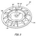
- FIG. 3is a perspective view of a wireless substrate-like particle sensor 300 in accordance with an embodiment of the present invention.
- Sensor 300bears many similarities to sensors 100 and 200 , and like components are numbered similarly.
- Sensor 300has an electronics enclosure 104 with a recessed surface 302 . Within electronics enclosure 104 below surface 302 , all of the electronics, such as those illustrated in FIG. 2 , are disposed.
- the embodiment illustrated in FIG. 3provides an optical technique for measuring particles proximate sensor 300 .
- particle sensor 214includes light source 304 disposed near the center of surface 302 .
- Light source 304may be an LED, a laser, or any other suitable light source.
- At least one illumination sensor 306is disposed near a periphery of surface 302 .
- a number of mirrors(shown in FIG. 4 ) be included near the periphery of surface 302 . Illumination emanating from source 304 essentially travels out in all directions, and, when no particles are present, generates substantially constant illumination signals at each of sensors 306 . When one or more particles enters the area between source 304 and one of detectors 306 , that detector 306 will note a fluctuation in the light intensity. This fluctuation can increment the particle count, or be stored in some other suitable fashion. While FIG.
- source 304may generate one or more directional beams, whether comprised of structured illumination or not, that may interact with one or more mirrors before finally impinging upon a detector 306 . In this way, more of the area proximate surface 302 can be monitored for interactions with particles.
- FIG. 3also illustrates optional electrode 216 in the form of a relatively large plate.
- Electrode 216is preferably an electrostatic electrode that is maintained, in known fashion, at a potential that will attract particles.
- FIG. 3illustrates one or more beams or rays of illumination moving from a static source to a plurality of static sensors
- one or more beamscould be scanned, or otherwise passed proximate surface 302 , for example by using moving mirrors.
- the beam or illuminationmay be collimated vertically, but diverging horizontally so that the angular coverage is enhanced without their physical scanning.
- FIG. 4is a top plan view illustrating sensor 300 in accordance with an embodiment of the present invention.
- Source 304generates illumination in directions 310 , 312 , 314 and 316 .
- Illumination 312is illustrated impinging a particle 318 , which is shown with a grossly exaggerated size.
- a portion of the illuminationis then deflected as illustrated at line 320 , and only illumination 322 reaches detector 306 .
- Detector 306senses this momentary change in illumination intensity, and registers a particle to controller 208 .
- FIG. 4also illustrates a number of mirrors 324 that help facilitate or otherwise generate larger optical paths along the plane proximate and substantially parallel to surface 302 .
- the illumination described with respect to the embodiments illustrated in FIGS. 3 and 4can take any suitable form, it is preferred that the illumination have a relatively short wavelength, such as in the blue, or even ultraviolet spectral range, since longer wavelength illumination will be less scattered by the very small particles. Accordingly, short wavelength illumination is preferable since process technology is advancing to smaller and smaller critical dimensions.
- the optical-based embodiment described with respect to FIGS. 3 and 4generally measure light emanating from a central source, one or more sensors can be used or arranged such that they do not normally see light from the centralized source, but instead see light from scattered particle interactions. Accordingly, in such embodiments, when there is no particle in the beam, there is not scattered light detected. Conversely, when there is a particle in the beam, scattered light is detected.
- combinations of detectors detecting both non-scattered and scattered lightcan be used to reduce the likelihood of false particle detentions.
- FIG. 5is a perspective view of a wireless substrate-like particle sensor in accordance with another embodiment of the present invention.
- Sensor 400bears some similarities to sensors 100 and 300 , and like components are numbered similarly.
- Sensor 400differs from previously-described sensors in that sensor 400 determines particle quantity by essentially measuring the mass of particles that adhere to structure 402 .
- Structure 402is preferably a microelectromechanical system (MEMS) that includes a piezoelectric element that is able to excite, or otherwise drive, structure 402 in order to determine its resonant frequency. As particles adhere to structure 402 , the mass of the combined particles/structure 402 will change, and accordingly change the resonant frequency.
- MEMSmicroelectromechanical system
- sensor 400include optional electrostatic electrode 216 disposed on structure 402 .
- optional electrostatic electrode 216disposed on structure 402 .
- particles floating proximate structure 402will be urged, via electrostatic force, to adhere to structure 402 .
- Structure 402then uses the electrostatic charge from optional electrode 216 to attract particles onto its beam or onto a proof of mass of structure 402 . While it is preferred that electrode 216 maintain either a positive or negative charge, it may also alternate to attract particles and potentially scavenge particles from the semiconductor processing tool.
- FIG. 6is a diagrammatic view of the MEMS mass-based embodiment described with respect to FIG. 5 .
- structure 402is a cantilever structure in that it is supported, as illustrated diagrammatically at support 406 , on or proximate one end.
- a portion of structure 402is piezoelectric, or otherwise formed of a suitable microelectromechanical structure such that a current from controller 208 through line 408 generates movement within structure 402 .
- controller 208Analyzing the electrical response of the piezoelectric element, controller 208 is able to calculate, or otherwise observe changes in, the mass of structure 402 , and/or the resonant frequency of structure 402 .
- FIG. 6also illustrates optional electrode 216 disposed on top of structure 402 and attracting particles 410 .
- Embodiments of the present inventiongenerally provide particle detection with a semiconductor processing tool that is in substantially real-time.
- This real-time feedbackcan be provided visually to a process engineer by virtue of the engineer viewing display 218 through a window in the process tool. Additionally, or alternatively, the real-time feedback can be provided via a radio frequency signal provided via radio frequency communication module 212 .
Landscapes
- Engineering & Computer Science (AREA)
- Microelectronics & Electronic Packaging (AREA)
- Condensed Matter Physics & Semiconductors (AREA)
- General Physics & Mathematics (AREA)
- Manufacturing & Machinery (AREA)
- Computer Hardware Design (AREA)
- Physics & Mathematics (AREA)
- Power Engineering (AREA)
- Multimedia (AREA)
- Signal Processing (AREA)
- Arrangements For Transmission Of Measured Signals (AREA)
- Testing Or Measuring Of Semiconductors Or The Like (AREA)
- Measurement Of Radiation (AREA)
- Investigating Or Analysing Materials By Optical Means (AREA)
Abstract
Description
- The present application is based on and claims the benefit of U.S. provisional patent application Ser. No. 60/848,336, filed Sep. 29, 2006, the content of which is hereby incorporated by reference in its entirety.
- The leading edge of the semiconductor processing industry is currently advancing production to the 65 nanometer and 45 nanometer nodes. Further, development is currently underway at the 32 nanometer and 22 nanometer nodes. Accordingly, it is increasingly critical that semiconductor processing tools and the processing itself be controlled to tolerances and conditions never previously required. The cost of wafer scrap and maintenance downtime continues to drive the desire to control processes and equipment to tighter levels, and as other problems arise that were insignificant to processes above 100 nanometers, process and equipment engineers look for new and innovative ways to better control semiconductor processing.
- During the manufacture of semiconductor wafers, there are multiple tools and process steps to which a wafer is exposed. During each of these steps there are potential defects that may be caused by dirty equipment and/or poor process conditions that can cause degradation in yield of the final integrated circuit devices due to microscopic particles being deposited on the wafer's surface. Thus, it is critical to keep all process stages and steps as clean as reasonably possible and to be able to monitor the condition of these various stages before committing wafers to the process. This is important because each wafer may contain the circuitry for tens or even hundreds of integrated circuit devices, and a single lost wafer may result in hundreds or thousands of dollars worth of scrap.
- Traditionally, wafers are test-run through the semiconductor processing tool and particles on the wafer are counted both before and after the test run. The difference in the number of particles is then attributed to the tool. This is a time-consuming process and may not provide any indication of where, within the tool, the particles were deposited. Accordingly, if too many particles are found on a given test run wafer, it simply indicates that the semiconductor processing tool is too dirty and that further technician efforts are required to open the tool, identify the source(s) of particles, and generate appropriate corrective action. Once this process is complete, the wafer must be test run again and the entire process repeated until there is simply an indication that the semiconductor processing tool is suitably clean.
- A substrate-like particle sensor includes a substrate-like base portion and an electronics enclosure disposed on the substrate-like base portion. A power source is located within the electronics enclosure. A controller is operably coupled to the power source. A particle sensor is operably coupled to the controller and provides an indication to the controller of at least one particle present near the particle sensor.
FIG. 1 is a perspective view of a wireless substrate-like sensor with which embodiments of the present invention are particularly useful.FIG. 2 is a block diagram of a wireless substrate-like particle sensor in accordance with an embodiment of the present invention.FIG. 3 is a perspective view of a wireless substrate-like particle sensor 300 in accordance with an embodiment of the present invention.FIG. 4 is a top plan view illustrating a sensor in accordance with an embodiment of the present invention.FIG. 5 is a perspective view of a wireless substrate-like particle sensor in accordance with another embodiment of the present invention.FIG. 6 is a diagrammatic view of the MEMS mass-based embodiment described with respect toFIG. 5 .- Embodiments of the present invention generally provide real-time sensing of particles present within the sealed environment of a semiconductor processing tool. The sensing of particles can be done in accordance with various techniques. One exemplary technique provided herein includes optically sensing particles proximate a substrate-like wireless sensor. Another embodiment includes sensing the mass of particles deposited upon a mechanical structure coupled to the wireless substrate-like sensor.
FIG. 1 is a perspective view of a wireless substrate-like sensor with which embodiments of the present invention are particularly useful.Sensor 100 includes substrate-like portion 102 that is preferably sized to have a diameter that is equal to that of a standard substrate size. Exemplary sizes include a 200 millimeter diameter, or a 300 millimeter diameter. However, as different standards are developed or employed, this dimension can vary.Sensor 100 includes electronics housing orenclosure 104 that is disposed upon substrate-like portion 102. In order to increase rigidity of theoverall sensor 100, a plurality of fins orstruts 106 are provided thatcouple side wall 108 ofelectronics enclosure 104 tosurface 110 of substrate-like portion 102. In order to pass easily through the sealed semiconductor processing chamber, it is desirable for substrate-like sensor 102 to have a form factor that is very similar, if not identical, to an actual substrate. Common wafer dimensions and characteristics may found in the following specification: SEMI M1-0302, “Specification for Polished Monochrystoline Silicon Wafers”, Semiconductor Equipment and Materials International, www.semi.org.FIG. 2 is a block diagram of a wireless substrate-like particle sensor in accordance with an embodiment of the present invention.Sensor 200 includeselectronics enclosure 202, which may be identical toenclosure 104. Disposed withinenclosure 202 arepower source 204,power management module 206, andcontroller 208. Additionally,memory 210 is also disposed withinenclosure 202 and is coupled tocontroller 208. Further still,radio frequency module 212 is disposed withinenclosure 202 and coupled tocontroller 208.- While
particle sensor 214 is illustrated inFIG. 2 as being disposed withinenclosure 202, it may form part ofenclosure 202, or may be disposed proximate, but external toenclosure 202. - As illustrated in
FIG. 2 ,power source 204 is preferably a battery disposed withinenclosure 202 and is coupled tocontroller 208 viapower management module 206. Preferably,power management module 206 is a power management integrated circuit available from Linear Technology Corporation under the trade designation LTC3443.Controller 208 is preferably a microprocessor available from Texas Instruments under the trade designation MSC1211Y5.Controller 208 is coupled tomemory module 210, which can take the form of any type of memory, including memory that is internal to controller208 as well as memory that is external to controller208. The preferred controller includes internal SRAM, flash RAM and boot ROM.Memory module 210 also preferably includes external flash memory having a size of 64K×8. Flash memory is useful for storing such non-volatile data as programs, calibration data, and/or non-changing data as may be required. The internal random access memory is useful for storing volatile data relevant to program operation. Controller 208 is coupled via a suitable port, such as a serial port, to radiofrequency communication module 212 in order to communicate with external devices. In one embodiment, radio-frequency module 212 operates in accordance with the well-known Bluetooth standard, Bluetooth core specification version 1.1 (Feb. 22, 2001), available from the Bluetooth SIG (www.bluethooth.com). One example ofmodule 212 is available form Mitsumi under the trade designation WMLC40. Additionally, other forms of wireless communication can be used in addition to, or instead of,module 212. Suitable examples of such wireless communication include any other form of radio frequency communication, acoustic communication, infrared communication or even communication employing magnetic induction.Controller 208 is coupled toparticle sensor 214 which is configured to sense one or more particlesproximate sensor 200 within the sealed environment of a semiconductor processing tool.Sensor 214 can preferably sense not only particle presence (in order to generate particle counts), but can also sense a characteristic of individual particles, such as mass and/or size. While an embodiment described below specifically addresses particle mass, particle size can be sensed by using a multi-pixel image sensor, such as a line sensor, or array, and detecting how many pixels sense the shadow of a particle.Sensor 200 can also includeoptional electrode 216 which preferably forms an electrostatic plate that is disposed to attract particles floating in the airproximate sensor 200 toparticle sensor 214 to be sensed more efficiently. The details of the way in whichoptional electrode 216 performs this function will be described with respect to distinct embodiments described below.Sensor 200 preferably includes adisplay 218 that is configured to provide a particle count and/or display a go/no go indication to the process engineer. Additionally, in order to reset the particle count,reset button 220 is also provided and is coupled tocontroller 208.FIG. 3 is a perspective view of a wireless substrate-like particle sensor 300 in accordance with an embodiment of the present invention.Sensor 300 bears many similarities tosensors Sensor 300 has anelectronics enclosure 104 with a recessedsurface 302. Withinelectronics enclosure 104 belowsurface 302, all of the electronics, such as those illustrated inFIG. 2 , are disposed. The embodiment illustrated inFIG. 3 provides an optical technique for measuring particlesproximate sensor 300. Specifically,particle sensor 214 includeslight source 304 disposed near the center ofsurface 302.Light source 304 may be an LED, a laser, or any other suitable light source. At least oneillumination sensor 306 is disposed near a periphery ofsurface 302. Further, it is preferred that a number of mirrors (shown inFIG. 4 ) be included near the periphery ofsurface 302. Illumination emanating fromsource 304 essentially travels out in all directions, and, when no particles are present, generates substantially constant illumination signals at each ofsensors 306. When one or more particles enters the area betweensource 304 and one ofdetectors 306, thatdetector 306 will note a fluctuation in the light intensity. This fluctuation can increment the particle count, or be stored in some other suitable fashion. WhileFIG. 3 illustratessource 304 as generating illumination in substantially all directions, it is expressly contemplated thatsource 304 may generate one or more directional beams, whether comprised of structured illumination or not, that may interact with one or more mirrors before finally impinging upon adetector 306. In this way, more of the areaproximate surface 302 can be monitored for interactions with particles.FIG. 3 also illustratesoptional electrode 216 in the form of a relatively large plate.Electrode 216 is preferably an electrostatic electrode that is maintained, in known fashion, at a potential that will attract particles.- While the embodiment illustrated with respect to
FIG. 3 illustrates one or more beams or rays of illumination moving from a static source to a plurality of static sensors, it is also expressly contemplated that one or more beams could be scanned, or otherwise passedproximate surface 302, for example by using moving mirrors. Further still, in either the embodiment shown inFIG. 3 , or the scanning beam embodiment, the beam or illumination may be collimated vertically, but diverging horizontally so that the angular coverage is enhanced without their physical scanning. FIG. 4 is a top planview illustrating sensor 300 in accordance with an embodiment of the present invention.Source 304 generates illumination indirections Illumination 312 is illustrated impinging aparticle 318, which is shown with a grossly exaggerated size. A portion of the illumination is then deflected as illustrated atline 320, andonly illumination 322 reachesdetector 306.Detector 306 senses this momentary change in illumination intensity, and registers a particle tocontroller 208.FIG. 4 also illustrates a number ofmirrors 324 that help facilitate or otherwise generate larger optical paths along the plane proximate and substantially parallel tosurface 302.- While the illumination described with respect to the embodiments illustrated in
FIGS. 3 and 4 can take any suitable form, it is preferred that the illumination have a relatively short wavelength, such as in the blue, or even ultraviolet spectral range, since longer wavelength illumination will be less scattered by the very small particles. Accordingly, short wavelength illumination is preferable since process technology is advancing to smaller and smaller critical dimensions. Further, while the optical-based embodiment described with respect toFIGS. 3 and 4 generally measure light emanating from a central source, one or more sensors can be used or arranged such that they do not normally see light from the centralized source, but instead see light from scattered particle interactions. Accordingly, in such embodiments, when there is no particle in the beam, there is not scattered light detected. Conversely, when there is a particle in the beam, scattered light is detected. Moreover, combinations of detectors detecting both non-scattered and scattered light can be used to reduce the likelihood of false particle detentions. FIG. 5 is a perspective view of a wireless substrate-like particle sensor in accordance with another embodiment of the present invention.Sensor 400 bears some similarities tosensors Sensor 400 differs from previously-described sensors in thatsensor 400 determines particle quantity by essentially measuring the mass of particles that adhere to structure402.Structure 402 is preferably a microelectromechanical system (MEMS) that includes a piezoelectric element that is able to excite, or otherwise drive,structure 402 in order to determine its resonant frequency. As particles adhere to structure402, the mass of the combined particles/structure 402 will change, and accordingly change the resonant frequency. In order to enhance the efficiency ofsensor 400, it is also preferred thatsensor 400 include optionalelectrostatic electrode 216 disposed onstructure 402. In this manner, particles floatingproximate structure 402 will be urged, via electrostatic force, to adhere to structure402.Structure 402 then uses the electrostatic charge fromoptional electrode 216 to attract particles onto its beam or onto a proof of mass ofstructure 402. While it is preferred thatelectrode 216 maintain either a positive or negative charge, it may also alternate to attract particles and potentially scavenge particles from the semiconductor processing tool.FIG. 6 is a diagrammatic view of the MEMS mass-based embodiment described with respect toFIG. 5 . Specifically,structure 402 is a cantilever structure in that it is supported, as illustrated diagrammatically atsupport 406, on or proximate one end. A portion ofstructure 402 is piezoelectric, or otherwise formed of a suitable microelectromechanical structure such that a current fromcontroller 208 throughline 408 generates movement withinstructure 402. Analyzing the electrical response of the piezoelectric element,controller 208 is able to calculate, or otherwise observe changes in, the mass ofstructure 402, and/or the resonant frequency ofstructure 402. This is because, as particles are deposited onstructure 402, as indicated atreference numeral 410, the total mass and rotational inertia of the system aboutsupport 206 changes. This change is then detected as the different resonant frequency.FIG. 6 also illustratesoptional electrode 216 disposed on top ofstructure 402 and attractingparticles 410.- Embodiments of the present invention generally provide particle detection with a semiconductor processing tool that is in substantially real-time. This real-time feedback can be provided visually to a process engineer by virtue of the
engineer viewing display 218 through a window in the process tool. Additionally, or alternatively, the real-time feedback can be provided via a radio frequency signal provided via radiofrequency communication module 212. - Although the present invention has been described with reference to preferred embodiments, workers skilled in the art will recognize that changes may be made in form and detail without departing from the spirit and scope of the invention.
Claims (15)
Priority Applications (1)
| Application Number | Priority Date | Filing Date | Title |
|---|---|---|---|
| US11/904,633US8823933B2 (en) | 2006-09-29 | 2007-09-27 | Substrate-like particle sensor |
Applications Claiming Priority (2)
| Application Number | Priority Date | Filing Date | Title |
|---|---|---|---|
| US84833606P | 2006-09-29 | 2006-09-29 | |
| US11/904,633US8823933B2 (en) | 2006-09-29 | 2007-09-27 | Substrate-like particle sensor |
Publications (2)
| Publication Number | Publication Date |
|---|---|
| US20080239314A1true US20080239314A1 (en) | 2008-10-02 |
| US8823933B2 US8823933B2 (en) | 2014-09-02 |
Family
ID=39268970
Family Applications (1)
| Application Number | Title | Priority Date | Filing Date |
|---|---|---|---|
| US11/904,633Active2028-04-25US8823933B2 (en) | 2006-09-29 | 2007-09-27 | Substrate-like particle sensor |
Country Status (8)
| Country | Link |
|---|---|
| US (1) | US8823933B2 (en) |
| JP (1) | JP5236652B2 (en) |
| KR (1) | KR101388304B1 (en) |
| CN (1) | CN101517701B (en) |
| DE (1) | DE112007002309T5 (en) |
| GB (1) | GB2455006A (en) |
| IL (1) | IL196520A0 (en) |
| WO (1) | WO2008042199A2 (en) |
Cited By (7)
| Publication number | Priority date | Publication date | Assignee | Title |
|---|---|---|---|---|
| WO2017078914A1 (en)* | 2015-11-06 | 2017-05-11 | Applied Materials, Inc. | Particle monitoring device |
| US20170221775A1 (en)* | 2016-01-28 | 2017-08-03 | Leonard TEDESCHI | Real time process characterization |
| US20170263511A1 (en)* | 2016-03-11 | 2017-09-14 | Leonard TEDESCHI | Wafer processing tool having a micro sensor |
| US20170365531A1 (en)* | 2016-06-20 | 2017-12-21 | Applied Materials, Inc. | Wafer processing equipment having capacitive micro sensors |
| WO2019209688A1 (en)* | 2018-04-24 | 2019-10-31 | Cyberoptics Corporation | Wireless substrate-like teaching sensor for semiconductor processing |
| WO2020064265A1 (en)* | 2018-09-24 | 2020-04-02 | Asml Netherlands B.V. | A process tool and an inspection method |
| TWI771609B (en)* | 2018-09-04 | 2022-07-21 | 美商應用材料股份有限公司 | Method and apparatus for measuring placement of a substrate on a heater pedestal |
Families Citing this family (7)
| Publication number | Priority date | Publication date | Assignee | Title |
|---|---|---|---|---|
| JP2011095022A (en)* | 2009-10-28 | 2011-05-12 | Koa Corp | Particle sensor |
| US11569138B2 (en) | 2015-06-16 | 2023-01-31 | Kla Corporation | System and method for monitoring parameters of a semiconductor factory automation system |
| US9725302B1 (en) | 2016-08-25 | 2017-08-08 | Applied Materials, Inc. | Wafer processing equipment having exposable sensing layers |
| WO2018073826A1 (en)* | 2016-10-22 | 2018-04-26 | Lapidot Matan | Mobile inspection system for the detection of defect occurrence and location |
| US10578510B2 (en) | 2016-11-28 | 2020-03-03 | Applied Materials, Inc. | Device for desorbing molecules from chamber walls |
| US10763143B2 (en) | 2017-08-18 | 2020-09-01 | Applied Materials, Inc. | Processing tool having a monitoring device |
| TW202212812A (en)* | 2020-06-04 | 2022-04-01 | 日商東京威力科創股份有限公司 | Inspection substrate, method for regenerating the same, and substrate processing apparatus |
Citations (85)
| Publication number | Priority date | Publication date | Assignee | Title |
|---|---|---|---|---|
| US3876833A (en)* | 1972-11-10 | 1975-04-08 | Trt Telecom Radio Electr | Receiver for synchronous data signals, including a detector for detecting transmission speed changes |
| US4074114A (en)* | 1976-03-12 | 1978-02-14 | Monarch Marking Systems, Inc. | Bar code and method and apparatus for interpreting the same |
| US4119381A (en)* | 1976-12-17 | 1978-10-10 | Eastman Kodak Company | Incubator and radiometric scanner |
| US4659220A (en)* | 1984-10-22 | 1987-04-21 | International Business Machines Corporation | Optical inspection system for semiconductor wafers |
| US4701096A (en)* | 1986-03-05 | 1987-10-20 | Btu Engineering Corporation | Wafer handling station |
| US4753569A (en)* | 1982-12-28 | 1988-06-28 | Diffracto, Ltd. | Robot calibration |
| US4843287A (en)* | 1987-12-31 | 1989-06-27 | Westinghouse Electric Corp. | Path contriving system for look-ahead sensor in a robotic control system |
| US5232331A (en)* | 1987-08-07 | 1993-08-03 | Canon Kabushiki Kaisha | Automatic article feeding system |
| US5265957A (en)* | 1992-08-11 | 1993-11-30 | Texas Instruments Incorporated | Wireless temperature calibration device and method |
| US5267143A (en)* | 1984-10-12 | 1993-11-30 | Sensor Adaptive Machines, Incorporated | Vision assisted fixture construction |
| US5298363A (en)* | 1991-06-17 | 1994-03-29 | Eastman Kodak Company | Photolithographically patterned fluorescent coating |
| US5301248A (en)* | 1987-11-09 | 1994-04-05 | Hitachi, Ltd. | Method for pattern inspection and apparatus therefor |
| US5321989A (en)* | 1990-02-12 | 1994-06-21 | Fraunhofer-Gesellschaft Zur Forderung Der Angewandten Forschung E.V. | Integratable capacitative pressure sensor and process for its manufacture |
| US5435682A (en)* | 1987-10-15 | 1995-07-25 | Advanced Semiconductor Materials America, Inc. | Chemical vapor desposition system |
| US5444637A (en)* | 1993-09-28 | 1995-08-22 | Advanced Micro Devices, Inc. | Programmable semiconductor wafer for sensing, recording and retrieving fabrication process conditions to which the wafer is exposed |
| US5521123A (en)* | 1992-04-17 | 1996-05-28 | Terumo Kabushiki Kaisha | Infrared sensor and method for production thereof |
| US5573728A (en)* | 1992-06-04 | 1996-11-12 | Gaz De France | Device for selective detection of gas |
| US5576831A (en)* | 1994-06-20 | 1996-11-19 | Tencor Instruments | Wafer alignment sensor |
| US5619027A (en)* | 1995-05-04 | 1997-04-08 | Intermec Corporation | Single width bar code symbology with full character set utilizing robust start/stop characters and error detection scheme |
| US5642293A (en)* | 1996-06-03 | 1997-06-24 | Camsys, Inc. | Method and apparatus for determining surface profile and/or surface strain |
| US5675396A (en)* | 1993-11-30 | 1997-10-07 | Matsushita Electric Industrial Co., Ltd. | Liquid crystal display unit having grounding frame |
| US5726066A (en)* | 1994-03-10 | 1998-03-10 | Lg Electronics Inc. | Method for manufacturing an infrared sensor array |
| US5742702A (en)* | 1992-10-01 | 1998-04-21 | Sony Corporation | Neural network for character recognition and verification |
| US5783341A (en)* | 1994-05-25 | 1998-07-21 | Canon Kabushiki Kaisha | Alignment for layer formation through determination of target values for translation, rotation and magnification |
| US5786704A (en)* | 1995-04-13 | 1998-07-28 | Mirae Corporation | Metallic tray unit for testing a semiconductor device |
| US5805289A (en)* | 1997-07-07 | 1998-09-08 | General Electric Company | Portable measurement system using image and point measurement devices |
| US5956417A (en)* | 1982-02-16 | 1999-09-21 | Sensor Adaptive Machines, Inc. | Robot vision using target holes, corners and other object features |
| US5962909A (en)* | 1996-09-12 | 1999-10-05 | Institut National D'optique | Microstructure suspended by a microsupport |
| US5969639A (en)* | 1997-07-28 | 1999-10-19 | Lockheed Martin Energy Research Corporation | Temperature measuring device |
| US5973788A (en)* | 1995-10-12 | 1999-10-26 | Metronor Asa | System for point-by-point measuring of spatial coordinates |
| US5981116A (en)* | 1996-12-12 | 1999-11-09 | Nikon Corporation | Alignment in a projection exposure method |
| US6010009A (en)* | 1995-10-13 | 2000-01-04 | Empak, Inc. | Shipping and transport cassette with kinematic coupling |
| US6013236A (en)* | 1996-10-03 | 2000-01-11 | Bridgestone Corporation | Wafer |
| US6022811A (en)* | 1990-12-28 | 2000-02-08 | Mitsubishi Denki Kabushiki Kaisha | Method of uniform CVD |
| US6075909A (en)* | 1998-06-26 | 2000-06-13 | Lucent Technologies, Inc. | Optical monitoring system for III-V wafer processing |
| US6106457A (en)* | 1997-04-04 | 2000-08-22 | Welch Allyn, Inc. | Compact imaging instrument system |
| US6129278A (en)* | 1994-05-19 | 2000-10-10 | Metanetics Corporation | Detecting image cell position with subpixel accuracy |
| US6175124B1 (en)* | 1998-06-30 | 2001-01-16 | Lsi Logic Corporation | Method and apparatus for a wafer level system |
| US6206441B1 (en)* | 1999-08-03 | 2001-03-27 | Taiwan Semiconductor Manufacturing Company, Ltd. | Apparatus and method for transferring wafers by robot |
| US6232615B1 (en)* | 1998-03-31 | 2001-05-15 | Asm Lithography B.V. | Lithographic projection apparatus with improved substrate holder |
| US6244121B1 (en)* | 1998-03-06 | 2001-06-12 | Applied Materials, Inc. | Sensor device for non-intrusive diagnosis of a semiconductor processing system |
| US6275742B1 (en)* | 1999-04-16 | 2001-08-14 | Berkeley Process Control, Inc. | Wafer aligner system |
| US6300974B1 (en)* | 1997-02-28 | 2001-10-09 | Commissariat A L'energie Atomique | Process and device for locating an object in space |
| US20010034222A1 (en)* | 2000-03-27 | 2001-10-25 | Alex Roustaei | Image capture and processing accessory |
| US20020006675A1 (en)* | 2000-05-17 | 2002-01-17 | Toshiyuki Shigaraki | Semiconductor manufacturing apparatus and method of manufacturing semiconductor devices |
| US20020016068A1 (en)* | 2000-08-07 | 2002-02-07 | Hiroyuki Nakano | Method and its apparatus for detecting floating particles in a plasma processing chamber and an apparatus for processing a semiconductor device |
| US20020028629A1 (en)* | 1998-08-31 | 2002-03-07 | Moore Scott E. | Method and apparatus for wireless transfer of chemical-mechanical planarization measurements |
| US20020101508A1 (en)* | 2001-01-30 | 2002-08-01 | Greene, Tweed Of Delaware, Inc. | Monitoring system for hostile environment |
| US6466325B1 (en)* | 1999-07-08 | 2002-10-15 | Bae Systems Plc | Method and apparatus for calibrating positions of a plurality of first light sources on a first part |
| US20020148307A1 (en)* | 2001-03-14 | 2002-10-17 | Jonkers Otto Cornelis | Inspection system for process devices for treating substrates, sensor intended for such inspection system, and method for inspecting process devices |
| US6476825B1 (en)* | 1998-05-13 | 2002-11-05 | Clemens Croy | Hand-held video viewer and remote control device |
| US6480537B1 (en)* | 1999-02-25 | 2002-11-12 | Telcordia Technologies, Inc. | Active techniques for video transmission and playback |
| US20030001083A1 (en)* | 2001-06-28 | 2003-01-02 | Greene Tweed Of Delaware, Inc. | Self contained sensing apparatus and system |
| US6526668B1 (en)* | 1999-03-11 | 2003-03-04 | Microtool, Inc. | Electronic level |
| US6532403B2 (en)* | 2000-04-21 | 2003-03-11 | Microtool, Inc | Robot alignment system and method |
| US6535650B1 (en)* | 1998-07-21 | 2003-03-18 | Intel Corporation | Creating high resolution images |
| US20030112448A1 (en)* | 2000-05-16 | 2003-06-19 | Armin Maidhof | Method and device for determining the 3d profile of an object |
| US6614215B1 (en)* | 1998-05-16 | 2003-09-02 | Microbial Systems Limited | Particle detection system and components thereof |
| US6681151B1 (en)* | 2000-12-15 | 2004-01-20 | Cognex Technology And Investment Corporation | System and method for servoing robots based upon workpieces with fiducial marks using machine vision |
| US6691068B1 (en)* | 2000-08-22 | 2004-02-10 | Onwafer Technologies, Inc. | Methods and apparatus for obtaining data for process operation, optimization, monitoring, and control |
| US6801257B2 (en)* | 2001-01-12 | 2004-10-05 | Cognitens Ltd. | Optical three-dimensional digital imaging and mensuration system for industrial applications |
| US6852975B2 (en)* | 2000-04-07 | 2005-02-08 | Riegl Laser Measurement Systems Gmbh | Method for the recording of an object space |
| US20050086024A1 (en)* | 2003-09-19 | 2005-04-21 | Cyberoptics Semiconductor Inc. | Semiconductor wafer location sensing via non contact methods |
| US6925356B2 (en)* | 1999-04-19 | 2005-08-02 | Applied Materials, Inc. | Method and apparatus for aligning a cassette |
| US6956230B1 (en)* | 1999-09-17 | 2005-10-18 | California Institute Of Technology | Integrated particles sensor formed on single substrate using fringes formed by diffractive elements |
| US6958768B1 (en)* | 2000-10-20 | 2005-10-25 | Asti Holdings Limited | CMOS inspection apparatus |
| US6966235B1 (en)* | 2000-10-06 | 2005-11-22 | Paton Eric N | Remote monitoring of critical parameters for calibration of manufacturing equipment and facilities |
| US20060000964A1 (en)* | 2003-03-18 | 2006-01-05 | Jun Ye | System and method for lithography process monitoring and control |
| US6985169B1 (en)* | 1998-02-09 | 2006-01-10 | Lenovo (Singapore) Pte. Ltd. | Image capture system for mobile communications |
| US20060017926A1 (en)* | 2003-07-23 | 2006-01-26 | Pochy Rocco D | Improved design for particle sensor system |
| US7035913B2 (en)* | 2001-09-28 | 2006-04-25 | Hewlett-Packard Development Company, L.P. | System for collection and distribution of calendar information |
| US20060151606A1 (en)* | 2002-02-06 | 2006-07-13 | Cyberoptics Semiconductor, Inc. | Wireless substrate-like sensor |
| US7108607B2 (en)* | 2003-06-05 | 2006-09-19 | Sps Technologies, Inc. | Helical groove fasteners and methods for making same |
| US7135852B2 (en)* | 2002-12-03 | 2006-11-14 | Sensarray Corporation | Integrated process condition sensing wafer and data analysis system |
| US20070044579A1 (en)* | 2005-08-26 | 2007-03-01 | Semiconductor Energy Laboratory Co., Ltd. | Particle detection sensor, method for manufacturing particle detection sensor, and method for detecting particle using particle detection sensor |
| US7206080B2 (en)* | 2001-07-30 | 2007-04-17 | Topcon Corporation | Surface shape measurement apparatus, surface shape measurement method, surface state graphic apparatus |
| US7222789B2 (en)* | 1997-10-17 | 2007-05-29 | Hand Held Products, Inc. | Bar code reading device having image processing mode |
| US20070194908A1 (en)* | 2006-02-17 | 2007-08-23 | Alejandro Ayala | Radio controlled clock and fire alarm safety |
| US20080018485A1 (en)* | 2006-07-18 | 2008-01-24 | Gentex Corporation | Optical particle detectors |
| US20080038810A1 (en)* | 2006-04-18 | 2008-02-14 | Pollack Michael G | Droplet-based nucleic acid amplification device, system, and method |
| US7360463B2 (en)* | 2002-01-24 | 2008-04-22 | Sensarray Corporation | Process condition sensing wafer and data analysis system |
| US20080160639A1 (en)* | 2006-12-29 | 2008-07-03 | Xina Su | Programmable electromagnetic array for molecule transport |
| US20090117555A1 (en)* | 2007-11-02 | 2009-05-07 | Franciscus Albertus Kuypers | Microfluidic Flow Lysometer Device, System and Method |
| US7757574B2 (en)* | 2002-01-24 | 2010-07-20 | Kla-Tencor Corporation | Process condition sensing wafer and data analysis system |
| US7993525B2 (en)* | 2006-12-29 | 2011-08-09 | Intel Corporation | Device and method for particle complex handling |
Family Cites Families (126)
| Publication number | Priority date | Publication date | Assignee | Title |
|---|---|---|---|---|
| US1668328A (en) | 1926-07-30 | 1928-05-01 | Bertha L Martien | Educational game board |
| SE358801B (en) | 1971-10-13 | 1973-08-06 | Ericsson Telefon Ab L M | |
| DE2158320B2 (en) | 1971-11-24 | 1980-04-10 | Ferdy Dr. Grenoble Mayer (Frankreich) | Device for non-contact relative distance measurement |
| FR39852E (en) | 1972-06-30 | 1932-03-24 | Ig Farbenindustrie Ag | Process for the production of solid dyes for vats |
| US3861981A (en) | 1973-01-24 | 1975-01-21 | Us Air Force | Portable etching system for holes drilled in metals |
| US4033053A (en) | 1976-01-14 | 1977-07-05 | Engler Theodore T | Digital segment display to braille converter |
| US4180199A (en) | 1978-02-27 | 1979-12-25 | Hollis Engineering, Inc. | Mass soldering control system |
| US4260258A (en) | 1978-08-14 | 1981-04-07 | Pacific Scientific Company | Compact, rugged sensor for optical measurement of the size of particles suspended in a fluid |
| JPS57120842A (en)* | 1981-01-19 | 1982-07-28 | Toshiba Corp | Detecting method for dust using electric charge coupling element |
| US4528451A (en) | 1982-10-19 | 1985-07-09 | Varian Associates, Inc. | Gap control system for localized vacuum processing |
| US4633578A (en) | 1983-12-01 | 1987-01-06 | Aine Harry E | Miniature thermal fluid flow sensors and batch methods of making same |
| CA1239785A (en) | 1984-03-14 | 1988-08-02 | John R. Shambroom | Capacitance height gage applied in reticle position detection system for electron beam lithography apparatus |
| US5374830A (en) | 1984-10-12 | 1994-12-20 | Sensor Adaptive Machines, Inc. | Target based determination of robot and sensor alignment |
| JPS62220833A (en)* | 1986-03-22 | 1987-09-29 | Sigma Tec:Kk | Light scatter type particulate sensor |
| US4746215A (en) | 1986-04-24 | 1988-05-24 | Pacific Scientific Company | Particle counter air inlet assembly |
| US4918627A (en) | 1986-08-04 | 1990-04-17 | Fmc Corporation | Computer integrated gaging system |
| US4810996A (en) | 1986-10-28 | 1989-03-07 | Jeffrey Glen | Patient communication and diagnostic device |
| US4791482A (en) | 1987-02-06 | 1988-12-13 | Westinghouse Electric Corp. | Object locating system |
| US4891030A (en) | 1988-04-28 | 1990-01-02 | Superior Toy & Manufacturing Company, Inc. | Toy with lighted playpieces |
| US4880384A (en) | 1989-02-03 | 1989-11-14 | Murphy Kevin C | Braille teaching apparatus |
| US4984889A (en) | 1989-03-10 | 1991-01-15 | Pacific Scientific Company | Particle size measuring system with coincidence detection |
| US5248553A (en) | 1989-03-16 | 1993-09-28 | Toyo Ink Manufacturing Co., Ltd. | Coated molded article |
| US4985601A (en) | 1989-05-02 | 1991-01-15 | Hagner George R | Circuit boards with recessed traces |
| US5055637A (en) | 1989-05-02 | 1991-10-08 | Hagner George R | Circuit boards with recessed traces |
| US5033851A (en) | 1989-05-30 | 1991-07-23 | Pacific Scientific Company | Light scattering method and apparatus for detecting particles in liquid sample |
| US5011286A (en) | 1989-08-03 | 1991-04-30 | Met One, Inc. | Multisensor particle counter utilizing a single energy source |
| JPH03108635A (en)* | 1989-09-22 | 1991-05-08 | Kondo Kogyo Kk | Monitoring alarm for particulates in the air |
| US5061065A (en) | 1989-10-20 | 1991-10-29 | Pacific Scientific Company | Particle contamination detection in fluids through the external section of a laser |
| US5092675A (en) | 1989-11-14 | 1992-03-03 | Pacific Scientific Company | Vacuum line particle detector with slab laser |
| CA2030139C (en) | 1989-11-20 | 2002-04-23 | David M. Durlach | 3-d amusement and display device |
| US5076794A (en) | 1991-04-29 | 1991-12-31 | Compaq Computer Corporation | Space-saving mounting interconnection between electrical components and a printed circuit board |
| US5175601A (en) | 1991-10-15 | 1992-12-29 | Electro-Optical Information Systems | High-speed 3-D surface measurement surface inspection and reverse-CAD system |
| JP3029916B2 (en) | 1992-03-07 | 2000-04-10 | キヤノン株式会社 | Information processing device |
| US5371585A (en) | 1992-11-10 | 1994-12-06 | Pacific Scientific Company | Particle detecting instrument with sapphire detecting cell defining a rectangular flow path |
| EP0598592B1 (en) | 1992-11-17 | 1999-09-01 | Seiko Epson Corporation | Optical head |
| USD344302S (en) | 1992-11-24 | 1994-02-15 | Interlego A.G. | Element for a toy buidling set |
| US5393706A (en) | 1993-01-07 | 1995-02-28 | Texas Instruments Incorporated | Integrated partial sawing process |
| US5382911A (en) | 1993-03-29 | 1995-01-17 | International Business Machines Corporation | Reaction chamber interelectrode gap monitoring by capacitance measurement |
| FR2706345B1 (en) | 1993-06-11 | 1995-09-22 | Bertin & Cie | Method and device for locating in space a mobile object such as a sensor or a tool carried by a robot. |
| FI93580C (en) | 1993-10-08 | 1995-04-25 | Vaisala Oy | Method and apparatus for feedback of an asymmetric pressure differential sensor |
| US5442297A (en) | 1994-06-30 | 1995-08-15 | International Business Machines Corporation | Contactless sheet resistance measurement method and apparatus |
| US5565984A (en) | 1995-06-12 | 1996-10-15 | Met One, Inc. | Re-entrant illumination system for particle measuring device |
| DE19633032B4 (en) | 1995-08-25 | 2007-01-04 | Volkswagen Ag | fastening system |
| US5642193A (en) | 1996-03-08 | 1997-06-24 | Met One, Inc. | Particle counter employing a solid-state laser with an intracavity view volume |
| US5798556A (en) | 1996-03-25 | 1998-08-25 | Motorola, Inc. | Sensor and method of fabrication |
| US6011294A (en) | 1996-04-08 | 2000-01-04 | Eastman Kodak Company | Low cost CCD packaging |
| NO303595B1 (en) | 1996-07-22 | 1998-08-03 | Metronor Asa | System and method for determining spatial coordinates |
| JP3108635B2 (en) | 1996-09-27 | 2000-11-13 | 株式会社佐賀鉄工所 | Bolt plate fixing structure |
| JPH10189675A (en)* | 1996-12-26 | 1998-07-21 | Toshiba Ceramics Co Ltd | Particle detection dummy wafer |
| US5839215A (en) | 1996-12-27 | 1998-11-24 | Lasprogata; Denise L. | Raised indicia labels |
| US6325356B1 (en) | 1997-05-05 | 2001-12-04 | Mag Aerospace Industries, Inc. | Long life rotary gate valve for aircraft vacuum toilet system |
| US6137572A (en) | 1998-02-27 | 2000-10-24 | Pacific Scientific Instruments Company | High sensitivity optical fluid-borne particle detection |
| JPH11328554A (en) | 1998-03-24 | 1999-11-30 | Pittway Corp | Smoke detector with particle sensor |
| JPH11330798A (en) | 1998-05-19 | 1999-11-30 | Fuji Mach Mfg Co Ltd | Method for mounting electric component and system thereof |
| JP2000019095A (en)* | 1998-06-30 | 2000-01-21 | Nec Kyushu Ltd | Device and method for measuring degree of cleanness of clean room |
| US6325536B1 (en) | 1998-07-10 | 2001-12-04 | Sensarray Corporation | Integrated wafer temperature sensors |
| US6111642A (en) | 1998-07-10 | 2000-08-29 | Pacific Scientific Instruments Company | Flow apertured intracavity laser particle detector |
| US5946093A (en) | 1998-08-19 | 1999-08-31 | Met One, Inc. | Particle detection system and method employing an upconversion laser |
| JP2000138274A (en)* | 1998-10-30 | 2000-05-16 | Tokyo Electron Ltd | Processing unit |
| US6628803B1 (en) | 1998-11-25 | 2003-09-30 | Pentax Corporation | Device for calculating positional data of standard points of photogrammetric target |
| JP2000227326A (en) | 1998-12-02 | 2000-08-15 | Nikon Corp | Flatness measuring device |
| JP4615726B2 (en) | 1998-12-04 | 2011-01-19 | ウェザーフォード/ラム インコーポレーテッド | Bragg grating pressure sensor |
| US6184773B1 (en) | 1998-12-07 | 2001-02-06 | Honeywell Inc. | Rugged fluid flow and property microsensor |
| TW364054B (en) | 1998-12-31 | 1999-07-11 | United Microelectronics Corp | Measurement tool for distance between shower head and heater platform |
| JP4794708B2 (en) | 1999-02-04 | 2011-10-19 | オリンパス株式会社 | 3D position and orientation sensing device |
| FR2793990B1 (en) | 1999-05-19 | 2001-07-27 | Sagem | ELECTRONIC HOUSING ON PLATE AND METHOD FOR MANUFACTURING SUCH A HOUSING |
| US6625305B1 (en) | 1999-08-16 | 2003-09-23 | Hewlett-Packard Development Company, L.P. | Image demosaicing method |
| US6373271B1 (en) | 1999-12-29 | 2002-04-16 | Motorola, Inc. | Semiconductor wafer front side pressure testing system and method therefor |
| AT409194B (en) | 2000-02-23 | 2002-06-25 | Riegl Laser Measurement Sys | METHOD FOR RECORDING AN OBJECT SPACE |
| US7120285B1 (en) | 2000-02-29 | 2006-10-10 | Advanced Micro Devices, Inc. | Method for evaluation of reticle image using aerial image simulator |
| JP2001338868A (en) | 2000-03-24 | 2001-12-07 | Nikon Corp | Illuminance measurement device and exposure device |
| US20030210041A1 (en) | 2000-04-07 | 2003-11-13 | Le Cuong Duy | Eddy current measuring system for monitoring and controlling a chemical vapor deposition (CVD) process |
| US6952656B1 (en) | 2000-04-28 | 2005-10-04 | Applied Materials, Inc. | Wafer fabrication data acquisition and management systems |
| WO2001091193A2 (en) | 2000-05-23 | 2001-11-29 | Atmel Corporation | Integrated ic chip package for electronic image sensor die |
| DE10035192C1 (en) | 2000-07-20 | 2001-10-11 | Carl Mahr Holding Gmbh | Capacitive displacement measuring system for length measurement, has capacitive sensor provided by differential capacitor with two partial capacitors supplied with phase opposed control signals |
| US6990215B1 (en) | 2000-07-31 | 2006-01-24 | Geodetic Services, Inc. | Photogrammetric measurement system and method |
| EP1184805A1 (en) | 2000-08-29 | 2002-03-06 | Motorola, Inc. | Electronic device for a wafer container, wafer manufacturing system, and method |
| US6465281B1 (en) | 2000-09-08 | 2002-10-15 | Motorola, Inc. | Method of manufacturing a semiconductor wafer level package |
| US20030160883A1 (en) | 2000-09-12 | 2003-08-28 | Viktor Ariel | Single chip cmos image sensor system with video compression |
| US6518775B1 (en) | 2000-11-15 | 2003-02-11 | Promos Technologies Inc. | Process for determining spacing between heater and showerhead |
| US6852988B2 (en) | 2000-11-28 | 2005-02-08 | Sumitomo Heavy Industries, Ltd. | Gap adjustment apparatus and gap adjustment method for adjusting gap between two objects |
| JP3694808B2 (en) | 2001-04-13 | 2005-09-14 | 株式会社安川電機 | Wafer transfer robot teaching method and teaching plate |
| US6859260B2 (en) | 2001-04-25 | 2005-02-22 | Asml Holding N.V. | Method and system for improving focus accuracy in a lithography system |
| JP2002357532A (en)* | 2001-06-01 | 2002-12-13 | Shimadzu Corp | Suspended particulate matter measurement device |
| US6607951B2 (en) | 2001-06-26 | 2003-08-19 | United Microelectronics Corp. | Method for fabricating a CMOS image sensor |
| FR2828560B1 (en) | 2001-08-09 | 2004-02-20 | Schlumberger Services Petrol | RESONANT OPTICALLY DRIVEN SENSOR AND MONITORING DEVICE USING THE SAME |
| DE10143075C2 (en) | 2001-09-03 | 2003-07-24 | Infineon Technologies Ag | Particle measuring device arrangement and device for processing semiconductor wafers with such an arrangement |
| US20090065429A9 (en) | 2001-10-22 | 2009-03-12 | Dickensheets David L | Stiffened surface micromachined structures and process for fabricating the same |
| DE10297565T5 (en)* | 2001-12-17 | 2005-01-05 | Cyberoptics Semiconductor, Inc., Beaverton | Mapping sensor for semiconductor wafer carriers |
| US6891276B1 (en) | 2002-01-09 | 2005-05-10 | Bridge Semiconductor Corporation | Semiconductor package device |
| US7142500B2 (en) | 2002-01-11 | 2006-11-28 | Hewlett-Packard Development Company, L.P. | Sensor with varying capacitance based on relative position between objects |
| IL147692A0 (en) | 2002-01-17 | 2002-08-14 | Innersense Ltd | Machine and environment analyzer |
| CA2369845A1 (en) | 2002-01-31 | 2003-07-31 | Braintech, Inc. | Method and apparatus for single camera 3d vision guided robotics |
| US20050224899A1 (en) | 2002-02-06 | 2005-10-13 | Ramsey Craig C | Wireless substrate-like sensor |
| US20050233770A1 (en) | 2002-02-06 | 2005-10-20 | Ramsey Craig C | Wireless substrate-like sensor |
| US20050224902A1 (en) | 2002-02-06 | 2005-10-13 | Ramsey Craig C | Wireless substrate-like sensor |
| JP2003344259A (en) | 2002-05-28 | 2003-12-03 | Rion Co Ltd | Particle detector |
| US6828542B2 (en)* | 2002-06-07 | 2004-12-07 | Brion Technologies, Inc. | System and method for lithography process monitoring and control |
| USD478494S1 (en) | 2002-09-20 | 2003-08-19 | Kevin D. Arnold | Replaceable, trimmable grip with pressure sensitive adhesive for tool handle |
| DE60236967D1 (en) | 2002-09-27 | 2010-08-19 | Rion Co | FLOW CELL AND PARTICLE MEASURING DEVICE THEREWITH |
| US6836212B2 (en) | 2002-10-10 | 2004-12-28 | Motorola, Inc. | Method and apparatus for reducing the likelihood of losing a portable electronic device |
| US6807503B2 (en) | 2002-11-04 | 2004-10-19 | Brion Technologies, Inc. | Method and apparatus for monitoring integrated circuit fabrication |
| EP1420264B1 (en) | 2002-11-15 | 2011-01-05 | Leica Geosystems AG | Method and device for calibrating a measurement system |
| US6949938B2 (en) | 2002-11-20 | 2005-09-27 | Taiwan Semiconductor Manufacturing Co., Ltd. | Prevention of robot damage via capacitive sensor assembly |
| US7151366B2 (en) | 2002-12-03 | 2006-12-19 | Sensarray Corporation | Integrated process condition sensing wafer and data analysis system |
| US6898558B2 (en) | 2002-12-31 | 2005-05-24 | Tokyo Electron Limited | Method and apparatus for monitoring a material processing system |
| US6815958B2 (en) | 2003-02-07 | 2004-11-09 | Multimetrixs, Llc | Method and apparatus for measuring thickness of thin films with improved accuracy |
| USD490276S1 (en) | 2003-02-21 | 2004-05-25 | Jorge M. Pereira | Transparent cake shield having candle apertures and handles |
| JP2004276151A (en) | 2003-03-13 | 2004-10-07 | Yaskawa Electric Corp | Transfer robot and transfer robot teaching method |
| US7355706B2 (en) | 2003-04-04 | 2008-04-08 | Hach Ultra Analytics, Inc. | Particle detection system implemented with an immersed optical system |
| US7144521B2 (en) | 2003-08-22 | 2006-12-05 | Lam Research Corporation | High aspect ratio etch using modulation of RF powers of various frequencies |
| US7002682B2 (en) | 2004-02-13 | 2006-02-21 | Hach Ultra Analytics, Inc. | Method and apparatus for operating a laser in an extinction-type optical particle detector |
| US7059936B2 (en) | 2004-03-23 | 2006-06-13 | Cabot Microelectronics Corporation | Low surface energy CMP pad |
| KR100614801B1 (en) | 2004-07-05 | 2006-08-22 | 삼성전자주식회사 | Film Formation Method of Semiconductor Device |
| US7502110B2 (en) | 2004-07-21 | 2009-03-10 | Lighthouse Worldwide Solutions, Inc | Design for particle sensor system |
| US20060055415A1 (en) | 2004-09-15 | 2006-03-16 | Mark Takita | Environmentally compensated capacitive sensor |
| US20060185432A1 (en) | 2005-01-13 | 2006-08-24 | Harvey Weinberg | Five degree of freedom intertial measurement device |
| JP2006214744A (en) | 2005-02-01 | 2006-08-17 | Gunma Univ | Biosensor and biosensor chip |
| US8167522B2 (en) | 2005-03-30 | 2012-05-01 | Brooks Automation, Inc. | Substrate transport apparatus with active edge gripper |
| US7682978B2 (en) | 2005-06-24 | 2010-03-23 | Tokyo Electron Limited | Plasma processing method and high-rate plasma etching apparatus |
| US7893697B2 (en) | 2006-02-21 | 2011-02-22 | Cyberoptics Semiconductor, Inc. | Capacitive distance sensing in semiconductor processing tools |
| US7804306B2 (en) | 2006-02-21 | 2010-09-28 | CyterOptics Semiconductor, Inc. | Capacitive distance sensing in semiconductor processing tools |
| JP2010506167A (en) | 2006-10-02 | 2010-02-25 | サイバーオプティクス セミコンダクタ インコーポレイテッド | Accelerometer with overlapping accelerometers |
| US7778793B2 (en) | 2007-03-12 | 2010-08-17 | Cyberoptics Semiconductor, Inc. | Wireless sensor for semiconductor processing systems |
| US20080246493A1 (en) | 2007-04-05 | 2008-10-09 | Gardner Delrae H | Semiconductor Processing System With Integrated Showerhead Distance Measuring Device |
| US20090015268A1 (en) | 2007-07-13 | 2009-01-15 | Gardner Delrae H | Device and method for compensating a capacitive sensor measurement for variations caused by environmental conditions in a semiconductor processing environment |
- 2007
- 2007-09-27GBGB0903833Apatent/GB2455006A/ennot_activeWithdrawn
- 2007-09-27JPJP2009530410Apatent/JP5236652B2/enactiveActive
- 2007-09-27DEDE112007002309Tpatent/DE112007002309T5/ennot_activeWithdrawn
- 2007-09-27CNCN2007800360927Apatent/CN101517701B/enactiveActive
- 2007-09-27WOPCT/US2007/020814patent/WO2008042199A2/enactiveApplication Filing
- 2007-09-27USUS11/904,633patent/US8823933B2/enactiveActive
- 2007-09-27KRKR1020097002270Apatent/KR101388304B1/enactiveActive
- 2009
- 2009-01-15ILIL196520Apatent/IL196520A0/enunknown
Patent Citations (100)
| Publication number | Priority date | Publication date | Assignee | Title |
|---|---|---|---|---|
| US3876833A (en)* | 1972-11-10 | 1975-04-08 | Trt Telecom Radio Electr | Receiver for synchronous data signals, including a detector for detecting transmission speed changes |
| US4074114A (en)* | 1976-03-12 | 1978-02-14 | Monarch Marking Systems, Inc. | Bar code and method and apparatus for interpreting the same |
| US4119381A (en)* | 1976-12-17 | 1978-10-10 | Eastman Kodak Company | Incubator and radiometric scanner |
| US5956417A (en)* | 1982-02-16 | 1999-09-21 | Sensor Adaptive Machines, Inc. | Robot vision using target holes, corners and other object features |
| US4753569A (en)* | 1982-12-28 | 1988-06-28 | Diffracto, Ltd. | Robot calibration |
| US5721677A (en)* | 1984-10-12 | 1998-02-24 | Sensor Adaptive Machines, Inc. | Vision assisted fixture construction |
| US5267143A (en)* | 1984-10-12 | 1993-11-30 | Sensor Adaptive Machines, Incorporated | Vision assisted fixture construction |
| US4659220A (en)* | 1984-10-22 | 1987-04-21 | International Business Machines Corporation | Optical inspection system for semiconductor wafers |
| US4701096A (en)* | 1986-03-05 | 1987-10-20 | Btu Engineering Corporation | Wafer handling station |
| US5232331A (en)* | 1987-08-07 | 1993-08-03 | Canon Kabushiki Kaisha | Automatic article feeding system |
| US5435682A (en)* | 1987-10-15 | 1995-07-25 | Advanced Semiconductor Materials America, Inc. | Chemical vapor desposition system |
| US5301248A (en)* | 1987-11-09 | 1994-04-05 | Hitachi, Ltd. | Method for pattern inspection and apparatus therefor |
| US4843287A (en)* | 1987-12-31 | 1989-06-27 | Westinghouse Electric Corp. | Path contriving system for look-ahead sensor in a robotic control system |
| US5321989A (en)* | 1990-02-12 | 1994-06-21 | Fraunhofer-Gesellschaft Zur Forderung Der Angewandten Forschung E.V. | Integratable capacitative pressure sensor and process for its manufacture |
| US6022811A (en)* | 1990-12-28 | 2000-02-08 | Mitsubishi Denki Kabushiki Kaisha | Method of uniform CVD |
| US5298363A (en)* | 1991-06-17 | 1994-03-29 | Eastman Kodak Company | Photolithographically patterned fluorescent coating |
| US5521123A (en)* | 1992-04-17 | 1996-05-28 | Terumo Kabushiki Kaisha | Infrared sensor and method for production thereof |
| US5573728A (en)* | 1992-06-04 | 1996-11-12 | Gaz De France | Device for selective detection of gas |
| US5265957A (en)* | 1992-08-11 | 1993-11-30 | Texas Instruments Incorporated | Wireless temperature calibration device and method |
| US5742702A (en)* | 1992-10-01 | 1998-04-21 | Sony Corporation | Neural network for character recognition and verification |
| US5444637A (en)* | 1993-09-28 | 1995-08-22 | Advanced Micro Devices, Inc. | Programmable semiconductor wafer for sensing, recording and retrieving fabrication process conditions to which the wafer is exposed |
| US5675396A (en)* | 1993-11-30 | 1997-10-07 | Matsushita Electric Industrial Co., Ltd. | Liquid crystal display unit having grounding frame |
| US5726066A (en)* | 1994-03-10 | 1998-03-10 | Lg Electronics Inc. | Method for manufacturing an infrared sensor array |
| US6129278A (en)* | 1994-05-19 | 2000-10-10 | Metanetics Corporation | Detecting image cell position with subpixel accuracy |
| US5783341A (en)* | 1994-05-25 | 1998-07-21 | Canon Kabushiki Kaisha | Alignment for layer formation through determination of target values for translation, rotation and magnification |
| US5576831A (en)* | 1994-06-20 | 1996-11-19 | Tencor Instruments | Wafer alignment sensor |
| US5786704A (en)* | 1995-04-13 | 1998-07-28 | Mirae Corporation | Metallic tray unit for testing a semiconductor device |
| US5619027A (en)* | 1995-05-04 | 1997-04-08 | Intermec Corporation | Single width bar code symbology with full character set utilizing robust start/stop characters and error detection scheme |
| US5973788A (en)* | 1995-10-12 | 1999-10-26 | Metronor Asa | System for point-by-point measuring of spatial coordinates |
| US6010009A (en)* | 1995-10-13 | 2000-01-04 | Empak, Inc. | Shipping and transport cassette with kinematic coupling |
| US5642293A (en)* | 1996-06-03 | 1997-06-24 | Camsys, Inc. | Method and apparatus for determining surface profile and/or surface strain |
| US5962909A (en)* | 1996-09-12 | 1999-10-05 | Institut National D'optique | Microstructure suspended by a microsupport |
| US6013236A (en)* | 1996-10-03 | 2000-01-11 | Bridgestone Corporation | Wafer |
| US5981116A (en)* | 1996-12-12 | 1999-11-09 | Nikon Corporation | Alignment in a projection exposure method |
| US6300974B1 (en)* | 1997-02-28 | 2001-10-09 | Commissariat A L'energie Atomique | Process and device for locating an object in space |
| US6106457A (en)* | 1997-04-04 | 2000-08-22 | Welch Allyn, Inc. | Compact imaging instrument system |
| US5805289A (en)* | 1997-07-07 | 1998-09-08 | General Electric Company | Portable measurement system using image and point measurement devices |
| US5969639A (en)* | 1997-07-28 | 1999-10-19 | Lockheed Martin Energy Research Corporation | Temperature measuring device |
| US7222789B2 (en)* | 1997-10-17 | 2007-05-29 | Hand Held Products, Inc. | Bar code reading device having image processing mode |
| US6985169B1 (en)* | 1998-02-09 | 2006-01-10 | Lenovo (Singapore) Pte. Ltd. | Image capture system for mobile communications |
| US20030209097A1 (en)* | 1998-03-06 | 2003-11-13 | Applied Materials, Inc. | Sensor device for non-intrusive diagnosis of a semiconductor processing system |
| US6468816B2 (en)* | 1998-03-06 | 2002-10-22 | Applied Materials, Inc. | Method for sensing conditions within a substrate processing system |
| US6244121B1 (en)* | 1998-03-06 | 2001-06-12 | Applied Materials, Inc. | Sensor device for non-intrusive diagnosis of a semiconductor processing system |
| US6232615B1 (en)* | 1998-03-31 | 2001-05-15 | Asm Lithography B.V. | Lithographic projection apparatus with improved substrate holder |
| US6476825B1 (en)* | 1998-05-13 | 2002-11-05 | Clemens Croy | Hand-held video viewer and remote control device |
| US6614215B1 (en)* | 1998-05-16 | 2003-09-02 | Microbial Systems Limited | Particle detection system and components thereof |
| US6075909A (en)* | 1998-06-26 | 2000-06-13 | Lucent Technologies, Inc. | Optical monitoring system for III-V wafer processing |
| US6175124B1 (en)* | 1998-06-30 | 2001-01-16 | Lsi Logic Corporation | Method and apparatus for a wafer level system |
| US6535650B1 (en)* | 1998-07-21 | 2003-03-18 | Intel Corporation | Creating high resolution images |
| US20020028629A1 (en)* | 1998-08-31 | 2002-03-07 | Moore Scott E. | Method and apparatus for wireless transfer of chemical-mechanical planarization measurements |
| US6480537B1 (en)* | 1999-02-25 | 2002-11-12 | Telcordia Technologies, Inc. | Active techniques for video transmission and playback |
| US6526668B1 (en)* | 1999-03-11 | 2003-03-04 | Microtool, Inc. | Electronic level |
| US6275742B1 (en)* | 1999-04-16 | 2001-08-14 | Berkeley Process Control, Inc. | Wafer aligner system |
| US6925356B2 (en)* | 1999-04-19 | 2005-08-02 | Applied Materials, Inc. | Method and apparatus for aligning a cassette |
| US7158857B2 (en)* | 1999-04-19 | 2007-01-02 | Applied Materials, Inc. | Method and apparatus for aligning a cassette |
| US6466325B1 (en)* | 1999-07-08 | 2002-10-15 | Bae Systems Plc | Method and apparatus for calibrating positions of a plurality of first light sources on a first part |
| US6206441B1 (en)* | 1999-08-03 | 2001-03-27 | Taiwan Semiconductor Manufacturing Company, Ltd. | Apparatus and method for transferring wafers by robot |
| US6956230B1 (en)* | 1999-09-17 | 2005-10-18 | California Institute Of Technology | Integrated particles sensor formed on single substrate using fringes formed by diffractive elements |
| US20010034222A1 (en)* | 2000-03-27 | 2001-10-25 | Alex Roustaei | Image capture and processing accessory |
| US6852975B2 (en)* | 2000-04-07 | 2005-02-08 | Riegl Laser Measurement Systems Gmbh | Method for the recording of an object space |
| US6532403B2 (en)* | 2000-04-21 | 2003-03-11 | Microtool, Inc | Robot alignment system and method |
| US20030112448A1 (en)* | 2000-05-16 | 2003-06-19 | Armin Maidhof | Method and device for determining the 3d profile of an object |
| US20020006675A1 (en)* | 2000-05-17 | 2002-01-17 | Toshiyuki Shigaraki | Semiconductor manufacturing apparatus and method of manufacturing semiconductor devices |
| US20020016068A1 (en)* | 2000-08-07 | 2002-02-07 | Hiroyuki Nakano | Method and its apparatus for detecting floating particles in a plasma processing chamber and an apparatus for processing a semiconductor device |
| US6691068B1 (en)* | 2000-08-22 | 2004-02-10 | Onwafer Technologies, Inc. | Methods and apparatus for obtaining data for process operation, optimization, monitoring, and control |
| US6966235B1 (en)* | 2000-10-06 | 2005-11-22 | Paton Eric N | Remote monitoring of critical parameters for calibration of manufacturing equipment and facilities |
| US6958768B1 (en)* | 2000-10-20 | 2005-10-25 | Asti Holdings Limited | CMOS inspection apparatus |
| US6681151B1 (en)* | 2000-12-15 | 2004-01-20 | Cognex Technology And Investment Corporation | System and method for servoing robots based upon workpieces with fiducial marks using machine vision |
| US6801257B2 (en)* | 2001-01-12 | 2004-10-05 | Cognitens Ltd. | Optical three-dimensional digital imaging and mensuration system for industrial applications |
| US20020101508A1 (en)* | 2001-01-30 | 2002-08-01 | Greene, Tweed Of Delaware, Inc. | Monitoring system for hostile environment |
| US6734027B2 (en)* | 2001-03-14 | 2004-05-11 | Asm International, N.V. | Inspection system for process devices for treating substrates, sensor intended for such inspection system, and method for inspecting process devices |
| US20020148307A1 (en)* | 2001-03-14 | 2002-10-17 | Jonkers Otto Cornelis | Inspection system for process devices for treating substrates, sensor intended for such inspection system, and method for inspecting process devices |
| US6603117B2 (en)* | 2001-06-28 | 2003-08-05 | Greene, Tweed & Co. | Self contained sensing apparatus and system |
| US20030127589A1 (en)* | 2001-06-28 | 2003-07-10 | Greene, Tweed & Co. | Self contained sensing apparatus and system |
| US20030001083A1 (en)* | 2001-06-28 | 2003-01-02 | Greene Tweed Of Delaware, Inc. | Self contained sensing apparatus and system |
| US7206080B2 (en)* | 2001-07-30 | 2007-04-17 | Topcon Corporation | Surface shape measurement apparatus, surface shape measurement method, surface state graphic apparatus |
| US7035913B2 (en)* | 2001-09-28 | 2006-04-25 | Hewlett-Packard Development Company, L.P. | System for collection and distribution of calendar information |
| US8033190B2 (en)* | 2002-01-24 | 2011-10-11 | Kla-Tencor Technologies Corporation | Process condition sensing wafer and data analysis system |
| US7819033B2 (en)* | 2002-01-24 | 2010-10-26 | Renken Wayne G | Process condition sensing wafer and data analysis system |
| US7757574B2 (en)* | 2002-01-24 | 2010-07-20 | Kla-Tencor Corporation | Process condition sensing wafer and data analysis system |
| US7360463B2 (en)* | 2002-01-24 | 2008-04-22 | Sensarray Corporation | Process condition sensing wafer and data analysis system |
| US20060171561A1 (en)* | 2002-02-06 | 2006-08-03 | Cyberoptics Semiconductor, Inc. | Wireless substrate-like sensor |
| US20060151606A1 (en)* | 2002-02-06 | 2006-07-13 | Cyberoptics Semiconductor, Inc. | Wireless substrate-like sensor |
| US7456977B2 (en)* | 2002-02-06 | 2008-11-25 | Cyberoptics Semiconductor, Inc. | Wireless substrate-like sensor |
| US7289230B2 (en)* | 2002-02-06 | 2007-10-30 | Cyberoptics Semiconductors, Inc. | Wireless substrate-like sensor |
| US7283255B2 (en)* | 2002-02-06 | 2007-10-16 | Cyberoptics Semiconductor, Inc. | Wireless substrate-like sensor |
| US7135852B2 (en)* | 2002-12-03 | 2006-11-14 | Sensarray Corporation | Integrated process condition sensing wafer and data analysis system |
| US20060000964A1 (en)* | 2003-03-18 | 2006-01-05 | Jun Ye | System and method for lithography process monitoring and control |
| US7108607B2 (en)* | 2003-06-05 | 2006-09-19 | Sps Technologies, Inc. | Helical groove fasteners and methods for making same |
| US20060017926A1 (en)* | 2003-07-23 | 2006-01-26 | Pochy Rocco D | Improved design for particle sensor system |
| US20050086024A1 (en)* | 2003-09-19 | 2005-04-21 | Cyberoptics Semiconductor Inc. | Semiconductor wafer location sensing via non contact methods |
| US20070044579A1 (en)* | 2005-08-26 | 2007-03-01 | Semiconductor Energy Laboratory Co., Ltd. | Particle detection sensor, method for manufacturing particle detection sensor, and method for detecting particle using particle detection sensor |
| US20070194908A1 (en)* | 2006-02-17 | 2007-08-23 | Alejandro Ayala | Radio controlled clock and fire alarm safety |
| US20080038810A1 (en)* | 2006-04-18 | 2008-02-14 | Pollack Michael G | Droplet-based nucleic acid amplification device, system, and method |
| US7616126B2 (en)* | 2006-07-18 | 2009-11-10 | Gentex Corporation | Optical particle detectors |
| US20080018485A1 (en)* | 2006-07-18 | 2008-01-24 | Gentex Corporation | Optical particle detectors |
| US20080160639A1 (en)* | 2006-12-29 | 2008-07-03 | Xina Su | Programmable electromagnetic array for molecule transport |
| US7993525B2 (en)* | 2006-12-29 | 2011-08-09 | Intel Corporation | Device and method for particle complex handling |
| US8105848B2 (en)* | 2006-12-29 | 2012-01-31 | Intel Corporation | Programmable electromagnetic array for molecule transport |
| US20090117555A1 (en)* | 2007-11-02 | 2009-05-07 | Franciscus Albertus Kuypers | Microfluidic Flow Lysometer Device, System and Method |
Cited By (20)
| Publication number | Priority date | Publication date | Assignee | Title |
|---|---|---|---|---|
| US10067070B2 (en) | 2015-11-06 | 2018-09-04 | Applied Materials, Inc. | Particle monitoring device |
| WO2017078914A1 (en)* | 2015-11-06 | 2017-05-11 | Applied Materials, Inc. | Particle monitoring device |
| US10718719B2 (en) | 2015-11-06 | 2020-07-21 | Applied Materials, Inc. | Particle monitoring device |
| US20170221775A1 (en)* | 2016-01-28 | 2017-08-03 | Leonard TEDESCHI | Real time process characterization |
| US11735486B2 (en) | 2016-01-28 | 2023-08-22 | Applied Materials, Inc. | Process monitor device having a plurality of sensors arranged in concentric circles |
| US10818561B2 (en)* | 2016-01-28 | 2020-10-27 | Applied Materials, Inc. | Process monitor device having a plurality of sensors arranged in concentric circles |
| US10818564B2 (en)* | 2016-03-11 | 2020-10-27 | Applied Materials, Inc. | Wafer processing tool having a micro sensor |
| US20170263511A1 (en)* | 2016-03-11 | 2017-09-14 | Leonard TEDESCHI | Wafer processing tool having a micro sensor |
| US11348846B2 (en) | 2016-03-11 | 2022-05-31 | Applied Materials, Inc. | Wafer processing tool having a micro sensor |
| US10083883B2 (en)* | 2016-06-20 | 2018-09-25 | Applied Materials, Inc. | Wafer processing equipment having capacitive micro sensors |
| US10923405B2 (en)* | 2016-06-20 | 2021-02-16 | Applied Materials, Inc. | Wafer processing equipment having capacitive micro sensors |
| US20170365531A1 (en)* | 2016-06-20 | 2017-12-21 | Applied Materials, Inc. | Wafer processing equipment having capacitive micro sensors |
| WO2019209688A1 (en)* | 2018-04-24 | 2019-10-31 | Cyberoptics Corporation | Wireless substrate-like teaching sensor for semiconductor processing |
| TWI771609B (en)* | 2018-09-04 | 2022-07-21 | 美商應用材料股份有限公司 | Method and apparatus for measuring placement of a substrate on a heater pedestal |
| US11404296B2 (en) | 2018-09-04 | 2022-08-02 | Applied Materials, Inc. | Method and apparatus for measuring placement of a substrate on a heater pedestal |
| TWI784325B (en)* | 2018-09-04 | 2022-11-21 | 美商應用材料股份有限公司 | Method and apparatus for measuring placement of a substrate on a heater pedestal |
| US11908724B2 (en) | 2018-09-04 | 2024-02-20 | Applied Materials, Inc. | Method and apparatus for measuring placement of a substrate on a heater pedestal |
| WO2020064265A1 (en)* | 2018-09-24 | 2020-04-02 | Asml Netherlands B.V. | A process tool and an inspection method |
| US11720032B2 (en) | 2018-09-24 | 2023-08-08 | Asml Netherlands B.V. | Process tool and an inspection method |
| TWI813768B (en)* | 2018-09-24 | 2023-09-01 | 荷蘭商Asml荷蘭公司 | Process tools for processing production substrates, methods for inspecting said process tools, and inspection substrate |
Also Published As
| Publication number | Publication date |
|---|---|
| CN101517701B (en) | 2011-08-10 |
| US8823933B2 (en) | 2014-09-02 |
| KR20090071539A (en) | 2009-07-01 |
| KR101388304B1 (en) | 2014-04-22 |
| WO2008042199A2 (en) | 2008-04-10 |
| WO2008042199A8 (en) | 2008-10-09 |
| JP2010505118A (en) | 2010-02-18 |
| JP5236652B2 (en) | 2013-07-17 |
| GB0903833D0 (en) | 2009-04-22 |
| WO2008042199A3 (en) | 2008-07-03 |
| GB2455006A (en) | 2009-05-27 |
| DE112007002309T5 (en) | 2009-07-30 |
| CN101517701A (en) | 2009-08-26 |
| IL196520A0 (en) | 2009-11-18 |
Similar Documents
| Publication | Publication Date | Title |
|---|---|---|
| US8823933B2 (en) | Substrate-like particle sensor | |
| US8045148B2 (en) | System for monitoring foreign particles, process processing apparatus and method of electronic commerce | |
| KR100727168B1 (en) | Substrate Inspection Apparatus and Method | |
| KR20030036897A (en) | Method and apparatus for enhanced embedded substrate inspection through process data collection and substrate imaging techniques | |
| JP6598782B2 (en) | Position sensitive substrate device | |
| US20070118300A1 (en) | Method and apparatus for cassette integrity testing using a wafer sorter | |
| JP2022504505A (en) | Deep learning-based adaptive region of interest for marginal dimensional measurements of semiconductor substrates | |
| KR100871495B1 (en) | Method and apparatus for automated process verification and hierarchical board inspection | |
| US7184134B2 (en) | Real-time monitoring apparatus for plasma process | |
| JP2020500415A (en) | Mobile inspection system for defect occurrence and location detection | |
| JPH10325807A (en) | Calibration standard sample for optical inspection device, method of manufacturing the same, and sensitivity calibration method in optical inspection device | |
| KR20190086261A (en) | Wafer-type gapping detection sensor for sensing gapping of the wafer in chamber | |
| US20230055839A1 (en) | Optical sensors for measuring properties of consumable parts in a semiconductor plasma processing chamber | |
| US11834642B2 (en) | Collection method for fine particles and collection system | |
| CN113466251B (en) | Equipment detection method and system | |
| KR102747750B1 (en) | Wafer type sensing apparatus and substrate treating apparatus including the same | |
| JPH11118677A (en) | Inspection object for calibration, manufacturing method thereof, calibration method of inspection device, and inspection device | |
| JP2006270111A (en) | Inspection method and apparatus for semiconductor device | |
| JP7755817B2 (en) | Optical sensor for measuring properties of consumable parts in semiconductor plasma processing chambers | |
| US8902412B2 (en) | Defect inspection apparatus and defect inspection method using the same | |
| JP2663955B2 (en) | Semiconductor manufacturing in-line particle detection device and semiconductor manufacturing device | |
| CN120418950A (en) | Substrate position monitoring device | |
| JP2005167210A (en) | Handling and processing system for wafer |
Legal Events
| Date | Code | Title | Description |
|---|---|---|---|
| AS | Assignment | Owner name:CYBEROPTICS CORPORATION, MINNESOTA Free format text:ASSIGNMENT OF ASSIGNORS INTEREST;ASSIGNORS:BONCIOLINI, DENNIS J.;RAMSEY, CRAIG C.;GARDNER, DELRAE H.;AND OTHERS;REEL/FRAME:020274/0847;SIGNING DATES FROM 20071205 TO 20071218 Owner name:CYBEROPTICS CORPORATION, MINNESOTA Free format text:ASSIGNMENT OF ASSIGNORS INTEREST;ASSIGNORS:BONCIOLINI, DENNIS J.;RAMSEY, CRAIG C.;GARDNER, DELRAE H.;AND OTHERS;SIGNING DATES FROM 20071205 TO 20071218;REEL/FRAME:020274/0847 | |
| AS | Assignment | Owner name:CYBEROPTICS SEMICONDUCTOR, INC., OREGON Free format text:ASSIGNMENT OF ASSIGNORS INTEREST;ASSIGNOR:CYBEROPTICS CORPORATION;REEL/FRAME:020375/0744 Effective date:20080115 | |
| STCF | Information on status: patent grant | Free format text:PATENTED CASE | |
| CC | Certificate of correction | ||
| MAFP | Maintenance fee payment | Free format text:PAYMENT OF MAINTENANCE FEE, 4TH YR, SMALL ENTITY (ORIGINAL EVENT CODE: M2551) Year of fee payment:4 | |
| AS | Assignment | Owner name:CYBEROPTICS CORPORATION, MINNESOTA Free format text:MERGER;ASSIGNOR:CYBEROPTICS SEMICONDUCTOR, INC;REEL/FRAME:045063/0120 Effective date:20140616 | |
| MAFP | Maintenance fee payment | Free format text:PAYMENT OF MAINTENANCE FEE, 8TH YR, SMALL ENTITY (ORIGINAL EVENT CODE: M2552); ENTITY STATUS OF PATENT OWNER: SMALL ENTITY Year of fee payment:8 | |
| FEPP | Fee payment procedure | Free format text:ENTITY STATUS SET TO UNDISCOUNTED (ORIGINAL EVENT CODE: BIG.); ENTITY STATUS OF PATENT OWNER: LARGE ENTITY |