US20080231625A1 - Display apparatus and drive method thereof and electronic device - Google Patents
Display apparatus and drive method thereof and electronic deviceDownload PDFInfo
- Publication number
- US20080231625A1 US20080231625A1US12/076,156US7615608AUS2008231625A1US 20080231625 A1US20080231625 A1US 20080231625A1US 7615608 AUS7615608 AUS 7615608AUS 2008231625 A1US2008231625 A1US 2008231625A1
- Authority
- US
- United States
- Prior art keywords
- drive transistor
- gate
- signal
- drive
- potential
- Prior art date
- Legal status (The legal status is an assumption and is not a legal conclusion. Google has not performed a legal analysis and makes no representation as to the accuracy of the status listed.)
- Granted
Links
Images


Classifications
- G—PHYSICS
- G09—EDUCATION; CRYPTOGRAPHY; DISPLAY; ADVERTISING; SEALS
- G09G—ARRANGEMENTS OR CIRCUITS FOR CONTROL OF INDICATING DEVICES USING STATIC MEANS TO PRESENT VARIABLE INFORMATION
- G09G3/00—Control arrangements or circuits, of interest only in connection with visual indicators other than cathode-ray tubes
- G09G3/20—Control arrangements or circuits, of interest only in connection with visual indicators other than cathode-ray tubes for presentation of an assembly of a number of characters, e.g. a page, by composing the assembly by combination of individual elements arranged in a matrix no fixed position being assigned to or needed to be assigned to the individual characters or partial characters
- G09G3/22—Control arrangements or circuits, of interest only in connection with visual indicators other than cathode-ray tubes for presentation of an assembly of a number of characters, e.g. a page, by composing the assembly by combination of individual elements arranged in a matrix no fixed position being assigned to or needed to be assigned to the individual characters or partial characters using controlled light sources
- G09G3/30—Control arrangements or circuits, of interest only in connection with visual indicators other than cathode-ray tubes for presentation of an assembly of a number of characters, e.g. a page, by composing the assembly by combination of individual elements arranged in a matrix no fixed position being assigned to or needed to be assigned to the individual characters or partial characters using controlled light sources using electroluminescent panels
- G09G3/32—Control arrangements or circuits, of interest only in connection with visual indicators other than cathode-ray tubes for presentation of an assembly of a number of characters, e.g. a page, by composing the assembly by combination of individual elements arranged in a matrix no fixed position being assigned to or needed to be assigned to the individual characters or partial characters using controlled light sources using electroluminescent panels semiconductive, e.g. using light-emitting diodes [LED]
- G09G3/3208—Control arrangements or circuits, of interest only in connection with visual indicators other than cathode-ray tubes for presentation of an assembly of a number of characters, e.g. a page, by composing the assembly by combination of individual elements arranged in a matrix no fixed position being assigned to or needed to be assigned to the individual characters or partial characters using controlled light sources using electroluminescent panels semiconductive, e.g. using light-emitting diodes [LED] organic, e.g. using organic light-emitting diodes [OLED]
- G09G3/3225—Control arrangements or circuits, of interest only in connection with visual indicators other than cathode-ray tubes for presentation of an assembly of a number of characters, e.g. a page, by composing the assembly by combination of individual elements arranged in a matrix no fixed position being assigned to or needed to be assigned to the individual characters or partial characters using controlled light sources using electroluminescent panels semiconductive, e.g. using light-emitting diodes [LED] organic, e.g. using organic light-emitting diodes [OLED] using an active matrix
- G09G3/3233—Control arrangements or circuits, of interest only in connection with visual indicators other than cathode-ray tubes for presentation of an assembly of a number of characters, e.g. a page, by composing the assembly by combination of individual elements arranged in a matrix no fixed position being assigned to or needed to be assigned to the individual characters or partial characters using controlled light sources using electroluminescent panels semiconductive, e.g. using light-emitting diodes [LED] organic, e.g. using organic light-emitting diodes [OLED] using an active matrix with pixel circuitry controlling the current through the light-emitting element
- G—PHYSICS
- G02—OPTICS
- G02F—OPTICAL DEVICES OR ARRANGEMENTS FOR THE CONTROL OF LIGHT BY MODIFICATION OF THE OPTICAL PROPERTIES OF THE MEDIA OF THE ELEMENTS INVOLVED THEREIN; NON-LINEAR OPTICS; FREQUENCY-CHANGING OF LIGHT; OPTICAL LOGIC ELEMENTS; OPTICAL ANALOGUE/DIGITAL CONVERTERS
- G02F1/00—Devices or arrangements for the control of the intensity, colour, phase, polarisation or direction of light arriving from an independent light source, e.g. switching, gating or modulating; Non-linear optics
- G02F1/01—Devices or arrangements for the control of the intensity, colour, phase, polarisation or direction of light arriving from an independent light source, e.g. switching, gating or modulating; Non-linear optics for the control of the intensity, phase, polarisation or colour
- G02F1/13—Devices or arrangements for the control of the intensity, colour, phase, polarisation or direction of light arriving from an independent light source, e.g. switching, gating or modulating; Non-linear optics for the control of the intensity, phase, polarisation or colour based on liquid crystals, e.g. single liquid crystal display cells
- G02F1/133—Constructional arrangements; Operation of liquid crystal cells; Circuit arrangements
- G—PHYSICS
- G09—EDUCATION; CRYPTOGRAPHY; DISPLAY; ADVERTISING; SEALS
- G09G—ARRANGEMENTS OR CIRCUITS FOR CONTROL OF INDICATING DEVICES USING STATIC MEANS TO PRESENT VARIABLE INFORMATION
- G09G3/00—Control arrangements or circuits, of interest only in connection with visual indicators other than cathode-ray tubes
- G09G3/20—Control arrangements or circuits, of interest only in connection with visual indicators other than cathode-ray tubes for presentation of an assembly of a number of characters, e.g. a page, by composing the assembly by combination of individual elements arranged in a matrix no fixed position being assigned to or needed to be assigned to the individual characters or partial characters
- G09G3/22—Control arrangements or circuits, of interest only in connection with visual indicators other than cathode-ray tubes for presentation of an assembly of a number of characters, e.g. a page, by composing the assembly by combination of individual elements arranged in a matrix no fixed position being assigned to or needed to be assigned to the individual characters or partial characters using controlled light sources
- G09G3/30—Control arrangements or circuits, of interest only in connection with visual indicators other than cathode-ray tubes for presentation of an assembly of a number of characters, e.g. a page, by composing the assembly by combination of individual elements arranged in a matrix no fixed position being assigned to or needed to be assigned to the individual characters or partial characters using controlled light sources using electroluminescent panels
- G09G3/32—Control arrangements or circuits, of interest only in connection with visual indicators other than cathode-ray tubes for presentation of an assembly of a number of characters, e.g. a page, by composing the assembly by combination of individual elements arranged in a matrix no fixed position being assigned to or needed to be assigned to the individual characters or partial characters using controlled light sources using electroluminescent panels semiconductive, e.g. using light-emitting diodes [LED]
- H—ELECTRICITY
- H05—ELECTRIC TECHNIQUES NOT OTHERWISE PROVIDED FOR
- H05B—ELECTRIC HEATING; ELECTRIC LIGHT SOURCES NOT OTHERWISE PROVIDED FOR; CIRCUIT ARRANGEMENTS FOR ELECTRIC LIGHT SOURCES, IN GENERAL
- H05B33/00—Electroluminescent light sources
- H05B33/12—Light sources with substantially two-dimensional radiating surfaces
- G—PHYSICS
- G09—EDUCATION; CRYPTOGRAPHY; DISPLAY; ADVERTISING; SEALS
- G09G—ARRANGEMENTS OR CIRCUITS FOR CONTROL OF INDICATING DEVICES USING STATIC MEANS TO PRESENT VARIABLE INFORMATION
- G09G2300/00—Aspects of the constitution of display devices
- G09G2300/08—Active matrix structure, i.e. with use of active elements, inclusive of non-linear two terminal elements, in the pixels together with light emitting or modulating elements
- G09G2300/0809—Several active elements per pixel in active matrix panels
- G09G2300/0819—Several active elements per pixel in active matrix panels used for counteracting undesired variations, e.g. feedback or autozeroing
- G—PHYSICS
- G09—EDUCATION; CRYPTOGRAPHY; DISPLAY; ADVERTISING; SEALS
- G09G—ARRANGEMENTS OR CIRCUITS FOR CONTROL OF INDICATING DEVICES USING STATIC MEANS TO PRESENT VARIABLE INFORMATION
- G09G2300/00—Aspects of the constitution of display devices
- G09G2300/08—Active matrix structure, i.e. with use of active elements, inclusive of non-linear two terminal elements, in the pixels together with light emitting or modulating elements
- G09G2300/0809—Several active elements per pixel in active matrix panels
- G09G2300/0842—Several active elements per pixel in active matrix panels forming a memory circuit, e.g. a dynamic memory with one capacitor
- G—PHYSICS
- G09—EDUCATION; CRYPTOGRAPHY; DISPLAY; ADVERTISING; SEALS
- G09G—ARRANGEMENTS OR CIRCUITS FOR CONTROL OF INDICATING DEVICES USING STATIC MEANS TO PRESENT VARIABLE INFORMATION
- G09G2310/00—Command of the display device
- G09G2310/02—Addressing, scanning or driving the display screen or processing steps related thereto
- G09G2310/0243—Details of the generation of driving signals
- G09G2310/0254—Control of polarity reversal in general, other than for liquid crystal displays
- G09G2310/0256—Control of polarity reversal in general, other than for liquid crystal displays with the purpose of reversing the voltage across a light emitting or modulating element within a pixel
- G—PHYSICS
- G09—EDUCATION; CRYPTOGRAPHY; DISPLAY; ADVERTISING; SEALS
- G09G—ARRANGEMENTS OR CIRCUITS FOR CONTROL OF INDICATING DEVICES USING STATIC MEANS TO PRESENT VARIABLE INFORMATION
- G09G2310/00—Command of the display device
- G09G2310/02—Addressing, scanning or driving the display screen or processing steps related thereto
- G09G2310/0264—Details of driving circuits
- G09G2310/0297—Special arrangements with multiplexing or demultiplexing of display data in the drivers for data electrodes, in a pre-processing circuitry delivering display data to said drivers or in the matrix panel, e.g. multiplexing plural data signals to one D/A converter or demultiplexing the D/A converter output to multiple columns
Definitions
- the present inventioncontains subject matter related to Japanese Patent Application JP 2007-074985 filed in the Japan Patent Office on Mar. 22, 2007, the entire contents of which being incorporated herein by reference.
- the present inventionrelates to a display apparatus of active matrix type based on light emitting devices used as pixels and the drive method thereof.
- the present inventionalso relates to an electronic device based on this display apparatus.
- the organic EL deviceis a light emitting device based on a phenomenon in which light is emitted when an electric field is impressed upon an organic thin film.
- the organic EL devicecan be driven on less than 10 V of applied voltage, so that this device involves low power dissipation.
- the organic EL deviceis self-luminous, so that no lighting member is required, thereby making this device light in weight and low in profile.
- the response speed of the organic EL deviceis as fast as several microseconds, thereby suppressing the generation of afterimage at displaying a moving image.
- related-art active matrix planar self-luminous display apparatusesinvolve a problem of causing the threshold voltage of the transistor for driving light emitting devices to fluctuate due to process variation. This characteristic fluctuation adversely affects light emitting luminance. Therefore, in order to uniformly control the light emitting luminance over the entire screen of the display apparatus, it is required to correct the threshold voltage fluctuation of the above-mentioned drive transistor in each pixel circuit.
- a display apparatus having such a threshold voltage correction capability for each pixelhas been proposed.
- a video signal with the threshold voltage correctedis sampled and the light emitting device is driven on the basis of the sampling.
- a current leakoccurs on the drive transistor between the threshold voltage correcting operation and the light emitting operation, which causes the threshold voltage correction to be not necessarily executed correctly, thereby involving an error.
- This error or fluctuation of the threshold voltage correctioncauses the unevenness in light emitting luminance, which in turn causes impaired picture quality.
- a display apparatusIn carrying out the invention and according to a first embodiment thereof, there is provided a display apparatus.
- This display apparatusis made up of a pixel array section and a drive section, the pixel array section having power supply lines, scan lines arranged in row, signal lines arranged in column, and pixels arranged in matrix at intersections of each of the scan lines and each of the signal lines, each of the pixels at least having a sampling transistor, a drive transistor, a light emitting device, and a capacitor.
- the sampling transistoris connected at a control terminal thereof to the scan line and at one of a pair of current terminals of the sampling transistor to the scan line and at the other of the pair of current terminals to a control terminal of the drive transistor.
- the drive transistoris connected at one of a pair of current terminals to the light emitting device and at the other of the pair of current terminals to the power supply line.
- the drive sectionsupplies a control signal to each scan line and a video signal to each signal line to drive each pixel, thereby executing a threshold voltage correcting operation for correcting a fluctuation of a threshold voltage of the drive transistor, a write operation for writing the video signal to the capacitor, and a light emitting operation for driving the light emitting device in accordance with the written video signal.
- the threshold voltage correcting operationhas a preparation process in which, while the control terminal that is a gate of the drive transistor is maintained at a reference potential, a gate-to-source voltage with the current terminal that is a source of the drive transistor is set higher than the threshold voltage to turn on the drive transistor, an energizing process in which the drive transistor is energized with the gate maintained at the reference potential to hold, in the capacitor, a voltage equivalent to the threshold voltage appearing between the gate and the source when the drive transistor is cut off, and a compression process in which the reference potential applied to the gate is varied to compress the gate-to-source voltage to higher level than the voltage equivalent to the threshold voltage to surely turn off the drive transistor.
- the drive sectionhas a write scanner for sequentially supplying control signals to scan lines for each horizontal scan period, a power supply scanner for switching each power supply line between high potential and low potential, and a signal driver for supplying a video signal in which a signal potential and a reference potential are switched in each horizontal scan period to each signal line.
- the write scanneroutputs a control signal to turn on the sampling transistor and samples the reference potential from the signal line to apply the sampled reference potential to the gate of the drive transistor
- the power supply scannerswitches the power supply line from high potential to low potential to lower a potential of the source of the drive transistor to low potential.
- the power supply scannerswitches the power supply line from low potential to high potential to energize the drive transistor until the drive transistor cuts off.
- the signal driverswitches a level of the reference potential downward immediately before the write scanner clears the control signal to turn off the sampling transistor while the power supply scanner maintains the power supply line at high potential.
- a display apparatusIn carrying out the invention and according to a second embodiment thereof, there is provided a display apparatus.
- This display apparatusis made up of a pixel array section and a drive section.
- the pixel array sectionhas power supply lines, scan lines arranged in row, signal lines arranged in column, and pixels arranged in matrix at intersections of each of the scan lines and each of the signal lines.
- Each of the pixelsat least has a sampling transistor, a drive transistor, a light emitting device, and a capacitor.
- the sampling transistoris connected at a control terminal thereof to the scan line and at one of a pair of current terminals of the sampling transistor to the scan line and at the other of the pair of current terminals to a control terminal of the drive transistor.
- the drive transistoris connected at one of a pair of current terminals to the light emitting device and at the other of the pair of current terminals to the power supply line.
- the drive sectionsupplies a control signal to each scan line and a video signal to each signal line to drive each pixel, thereby executing a threshold voltage correcting operation for correcting a fluctuation of a threshold voltage of the drive transistor, a write operation for writing the video signal to the capacitor, and a light emitting operation for emitting the light emitting device in accordance with the written video signal.
- the threshold voltage correcting operationhas a preparation process in which, while the control terminal that is a gate of the drive transistor is maintained at a reference potential, a gate-to-source voltage with the current terminal that is a source of the drive transistor is set higher than the threshold voltage to turn on the drive transistor and an energizing process in which the drive transistor is energized with the gate maintained at the reference potential to hold, in the capacitor, a voltage equivalent to the threshold voltage appearing between the gate and the source when the drive transistor is cut off.
- the energizing processis executed in a time division manner a plurality of times until the drive transistor cuts off, there being a difference between a reference potential to be applied to the gate of the drive transistor in a preceding energizing process and a reference potential to be applied to the gate of the drive transistor in a following energizing process.
- the energizing processis executed in a time division manner a plurality of times until the drive transistor cuts off and the reference potential to be applied to the gate of the drive transistor in the following energizing process becomes higher than the reference potential to be applied to the gate of the drive transistor in the preceding energizing process.
- the drive sectionhas a write scanner for sequentially supplying control signals to scan lines for each horizontal scan period, a power supply scanner for switching each power supply line between high potential and low potential, and a signal driver for supplying a video signal in which a signal potential and a reference potential are switched in each horizontal scan period to each signal line; in the preparation period, while the write scanner outputs a control signal to turn on the sampling transistor and samples the reference potential from the signal line to apply the sampled reference potential to the gate of the drive transistor, the power supply scanner switches the power supply line from low potential to high potential to lower a potential of the source of the drive transistor to low potential; and in the energizing process, the power supply scanner switches the power supply line from high potential to low potential to energize the drive transistor until the drive transistor cuts off.
- the signal driverexecutes switching control such that the reference potential to be outputted to the signal line in the following energizing processing is higher than the reference potential to be outputted to the signal line in the preceding energizing process.
- each pixelexecutes a drive transistor threshold voltage correcting operation before executing a video signal write operation and a light emitting device lighting operation.
- This threshold voltage correcting operationincludes a preparation process and an energizing process.
- the preparation processwhile he gate of the drive transistor is maintained at the reference potential, the gate-to-source voltage of the drive transistor is set higher than the threshold voltage to turn on the drive transistor.
- the drive transistoris energized with the gate maintained at the reference potential and, when the drive transistor cuts off, a voltage equivalent to the threshold voltage appearing between gate and source is held in the capacitor.
- the threshold voltage correcting operationhas a compression process after the above-mentioned preparation process and energizing process.
- the reference potential applied to the gate after the energizing processis varied to compress the gate-to-source voltage higher than the voltage equivalent to the threshold voltage, thereby surely turning off the drive transistor.
- This configurationprevents a leak current from flowing in the drive transistor, thereby stably maintaining results of the threshold voltage correcting operation until later write and light emitting operations.
- the fluctuation of the threshold voltage correcting operationis minimized to significantly enhance the accuracy. Consequently, the light emitting luminance has little fluctuation to significantly enhance the quality of screen.
- the energizing process of the threshold voltage correcting operationis executed in a time division manner a plurality of times until the drive transistor is cut off.
- This configurationcan give a sufficient energizing time, thereby surely allocating a voltage equivalent to the threshold voltage into the capacitor. In doing so, a difference is provided in the reference voltage level to be applied to the gate of the drive transistor between the preceding energizing process and the following energizing process.
- the reference voltage to be applied to the gate of the drive transistor in the following energizing processis set higher than that in the preceding energizing process.
- switching between the reference voltage levels in the energizing process executed in a time division mannercan suppress the current leak of the drive transistor, eventually stabilizing the threshold voltage correcting operation and enhancing the accuracy thereof. Consequently, the fluctuation of the light emitting luminance of each pixel is minimized to improve the uniformity of screen.
- FIG. 1is a block diagram illustrating an overall configuration of a display apparatus practiced as one embodiment of the invention
- FIG. 2is a circuit diagram illustrating an exemplary configuration of a pixel included in the display apparatus shown in FIG. 1 ;
- FIG. 3is a timing chart indicative of an operation of the display apparatus shown in FIGS. 1 and 2 ;
- FIG. 4is a timing chart indicative of another operation of the above-mentioned display apparatus
- FIG. 5is a timing chart indicative of a still another operation of the above-mentioned display apparatus
- FIG. 6is a circuit diagram illustrating an exemplary configuration of a horizontal sector (or a signal driver) included in the display apparatus shown in FIGS. 1 and 2 ;
- FIG. 7is a timing chart indicative of an operation of the signal driver shown in FIG. 6 ;
- FIG. 8is a timing chart indicative of another operation of the above-mentioned signal driver
- FIG. 9is a timing chart indicative of an operation of the display apparatus shown in FIGS. 1 and 2 ;
- FIG. 10is a timing chart indicative of another operation of the display apparatus shown in FIGS. 1 and 2 ;
- FIG. 11is an overall block diagram illustrating a display apparatus practiced as another embodiment of the invention.
- FIG. 12is a circuit diagram illustrating an exemplary configuration of a pixel included in the display apparatus shown in FIG. 11 ;
- FIG. 13is a circuit diagram illustrating an exemplary configuration of the pixel
- FIG. 14is a timing chart indicative of an operation of the display apparatus shown in FIG. 11 ;
- FIG. 15is a cross section illustrating a device configuration of the above-mentioned display apparatus
- FIG. 16is a top view illustrating a module configuration of the above-mentioned display apparatus
- FIG. 17is a perspective view illustrating a television set having the above-mentioned display apparatus
- FIG. 18is a perspective view illustrating a digital still camera having the above-mentioned display apparatus
- FIG. 19is a perspective view illustrating a note-type personal computer having the above-mentioned display apparatus
- FIG. 20is a schematic diagram illustrating a portable terminal apparatus having the above-mentioned display apparatus.
- FIG. 21is a perspective view illustrating a video camera having the above-mentioned display apparatus.
- FIG. 1there is shown an overall configuration of a display apparatus practiced as one embodiment of the invention.
- the display apparatusis made up of a pixel array block 1 and a drive block configured to drive the pixel array block 1 .
- the pixel array block 1has write scan lines WS arranged in row, signal lines SL arranged in column, pixels 2 each arranged in row at each intersection between the write scan line WS and the signal lines SL, and power supply lines DS each arranged for each row of pixels 2 .
- the drive blockhas a write scanner 4 for sequentially supplying control signals to the write scan lines to sequentially scanning pixels 2 on a row basis, a drive scanner 5 for supplying a supply voltage switching between high and low potentials for each power supply line DS in synchronization with this line sequential scan, and a horizontal selector 3 for supplying a signal potential providing a video signal and a reference potential to each of signal lines SL arranged in column in synchronization with this line sequential scan.
- the write scanner 4 and the drive scanner 5make up a scanner block and the horizontal selector 3 makes up a signal driver.
- Each pixel 2is made up of a sampling transistor Tr 1 , a drive transistor Trd, a storage capacitor (Cs), a sub capacitor (Csub), and a light emitting device EL.
- Each light emitting device ELis designed to emit light in one of three primary colors RGB.
- a pixel triois made up of a pixel (RED) having a red light emitting device, a pixel (GREEN) having a green light emitting device, and a pixel (BLUE) having a blue light emitting device. Arranging pixel trios on the pixel array block 1 in a matrix allows color display.
- FIG. 2shows a specific configuration of the pixel 2 included in the display apparatus shown in FIG. 1 and a line connection relationship of the pixel 2 .
- this pixel 2includes a light emitting device EL represented by an organic EL device for example, a sampling transistor Tr 1 , a drive transistor Trd, and a storage capacitor Cs.
- the sampling transistor Tr 1is connected at a gate thereof to the write scan line WS, at one of the source and drain thereof to a corresponding signal line SL, and at the other of the source and drain thereof to a gate G of the drive transistor Trd.
- the drive transistor Trdis connected at a source S thereof to the light emitting device EL, and at a drain thereof to a corresponding power supply line DS.
- a cathode of the light emitting device ELis connected to a ground potential Vcath. This ground wiring is common to all pixels 2 .
- the storage capacitor (or a pixel capacitor) Csis connected between the source S and the gate G of the drive transistor Trd.
- the sub capacitor Csubis connected in parallel to the light emitting device EL. This sub capacitor Csub, added as required, has a function of increasing an input gain of a video signal Vsig for the storage capacitor Cs.
- each pixel 2includes at least a sampling transistor Tr 1 , a drive transistor Trd, a light emitting device EL, and a storage capacitor Cs.
- the sampling transistor Tr 1is connected at a control terminal (or a gate) thereof to the write scan line WS and at a pair of current terminals (source and drain) thereof connected between the signal line SL and the control terminal of the drive transistor Trd.
- the drive transistor Trdis connected at one of the pair of current terminals (source and drain) to the light emitting device EL and at the other of the pair to the power supply line DS.
- the storage capacitor Csis connected between the control terminal (gate G) of the drive transistor Trd and one (source S) of a pair of current terminals (source and drain) of the drive transistor Trd.
- FIG. 3shows a timing chart indicative of an operation of the pixel 2 shown in FIG. 2 .
- this timing chartis not indicative of one embodiment of the invention, but is a first reference example indicative of an ideal operation status.
- This timing chartrepresents a potential change of scan line WS, a potential change of power supply line DS, and a potential change of signal line SL with reference to a common time axis. In parallel to these potential changes, changes of the gate G and the source S of the drive transistor Trd are also indicated.
- periods ( 0 ) to ( 7 )are provided in match with operational transitions of the pixel 2 .
- the power supply line DSis at high potential Vccp and the drive transistor Trd is supplying drive current Ids to the light emitting device EL.
- Drive current Idsflows from the power supply line DS that is at high potential Vccp into common ground line Vcath through the light emitting device EL via the drive transistor Trd.
- the power supply line DSis switched from high potential Vccp to low potential Vini. This discharges the power supply line DS to Vini and the source potential of the drive transistor Trd goes up to a potential near Vini. If the wiring capacity of the power supply line DS is relatively large, it is a good practice to switch the power supply line DS from high potential Vccp to low potential Vini as comparatively early as possible.
- period ( 2 )when the scan line WS is changed from low level to high level, the sampling transistor Tr 1 gets in a conduction state. At this moment, the signal line SL is at reference voltage Vofs. Therefore, the gate potential of the drive transistor Trd provides reference potential Vofs of the signal line SL through the conductive sampling transistor Tr 1 . At the same time, the source potential of the drive transistor Trd is fixed to low potential Vini. Consequently, the source potential of the drive transistor Trd is reset to potential Vini that is lower enough than reference voltage Vofs of the signal line SL. To be more specific, low potential Vini of the power supply line DS is set so as to make a potential between gate and source (or a difference between gate potential and source potential) of the drive transistor Trd greater than threshold voltage Vth of the drive transistor Trd.
- period ( 1 ) and period ( 2 )provide the preparatory processes for a threshold voltage correcting operation. Namely, in this preparatory process, while the control terminal that is the gate G of the drive transistor Trd is held at reference voltage Vofs, gate-to-source voltage Vgs between the current terminals that provide the source S of the drive transistor Trd is set higher than threshold voltage Vth, thereby turning on the drive transistor Trd.
- the power supply line DSshifts from low potential ini to high potential Vccp, upon which the source potential of the drive transistor Trd starts rising.
- Vccphigh potential
- Vththe gate/source voltage Vgs of the drive transistor Trd has reached threshold voltage Vth
- the currentis cut off.
- a voltage equivalent to the threshold voltage Vth of the drive transistor Trdis written to the storage capacitor (pixel capacitor) Cs. This is a threshold voltage correcting operation.
- the potential of common ground line Vcathis set in advance so as to cut off the light emitting device EL.
- this Vth cancel period ( 3 )provides the energizing process of a threshold voltage correcting operation.
- the drive transistor Trdis energized with the gate G held at reference potential Vofs and, when the drive transistor Trd is cut off, a voltage equivalent to the threshold voltage appearing between the gate and source of the drive transistor Trd is held in the storage capacitor Cs.
- the scan line WSshifts to the low potential size, upon which the sampling transistor Tr 1 goes off.
- the gate G of the drive transistor Trdfloats, but the gate-to-source voltage Vgs is in a cut off state because the gate-to-source voltage Vgs is equal to the threshold voltage Vth of the drive transistor Trd, no drain current Ids flowing.
- thisis an ideal state; actually, because the drive transistor Trd involves a current leak, the drain current Ids flows even though small. Consequently, the source potential of the drive transistor Trd fluctuates, thereby causing the potential of the floating gate G to fluctuate, which is referred to as a bootstrap phenomenon.
- the scan line WSshifts to the high potential side, upon which the sampling transistor Tr 1 is turned on. Therefore, the gate potential of the drive transistor Trd becomes signal potential Vsig. Since the light emitting device EL is in the cut off state (a high impedance state) beforehand, the drain-to-source current Ids of the drive transistor Trd flows into the light emitting device capacitor and the sub capacitor Csub, starting charging these capacitors. Therefore, the source potential of the drive transistor Trd starts rising and the gate-to-source voltage Vgs of the drive transistor Trd gradually becomes Vsig+Vth ⁇ V. Thus, the sampling of signal potential Vsig and the adjustment of correction amount ⁇ V are executed at the same time.
- VsigAs Vsig increases, Ids increases and also the absolute value of ⁇ V. Therefore, the mobility correction in accordance with light emitting luminance level is executed. If Vsig is constant, as the mobility ⁇ of the drive transistor Trd increases, the absolute value of ⁇ V increases. In other words, as the mobility ⁇ increases, negative feedback ⁇ V increases, so that the fluctuation of the mobility ⁇ for each pixel can be removed.
- the scan line WSshifts to the low potential side, upon which the sampling transistor Tr 1 is turned off. Consequently, the gate G of the drive transistor Trd is disconnected from the signal line SL.
- the drain current Idsstarts flowing in the light emitting device EL. This raises the anode potential of the light emitting device EL in accordance with the drive current Ids.
- the rise of the anode potential of the light emitting device ELis nothing but the use of the source potential of the drive transistor Trd.
- the gate potential of the drive transistor Trdalso rises by the bootstrap operation of the storage capacitor Cs.
- FIG. 4is a timing chart indicative of an operation of the display apparatus shown in FIGS. 1 and 2 .
- This timing chartis representative of the actual potential changes of gate G and source S deviated from an ideal state providing a second reference example.
- the same notation as that of the first reference example shown in FIG. 3is used.
- the scan line WSis lowered to turn off the sampling transistor Tr 1 .
- switching of the sampling transistor Tr 1couples the gate G, thereby fluctuating the potential of the gate G.
- the potential of source Sfluctuates.
- a leak currentflows between the drain and source of the drive transistor Trd. Affected by this leak, the source potential rises in the floating period ( 4 ). This causes the potential of the gate G to rise, too. This indicates that the same phenomenon as so-called bootstrap is taking place in this floating period ( 4 ).
- the control signalis applied to the scan line WS again to turn on the sampling transistor Tr 1 , thereby writing signal potential Vsig to the gate G of the drive transistor Trd.
- the potential of source Shas slightly risen, so that the potential is a source potential indicated by X at the time when the write period ( 6 ) has ended. Since the source potential S and the gate potential G have risen during the floating period ( 4 ) because of the leak, the source potential S at the time when the write period ( 6 ) has ended is not necessarily constant, being different from a pixel to another.
- the source-to-gate voltage Vgs of the drive transistor Trdfluctuates between pixels, causing a difference in light emitting luminance.
- the trend of the leak of the drive transistor Trdappears along the scan line WS (line), so that the fluctuation of Vgs results in a horizontal irregularity of stripes at the time of emitting, thereby impairing screen uniformity.
- the Vth cancel period ( 3 )may not be sufficiently allocated. Therefore, the fluctuation of Vth of the drive transistor Trd may not be sufficiently canceled. If this state is further affected by the fluctuation of the leak of the drive transistor Trd, Vgs fluctuates to a large degree, thereby deteriorating the unevenness of stripes.
- FIG. 5shows a timing chart indicative of an operation of the display apparatus shown in FIGS. 1 and 2 .
- This timing chartis representative of one embodiment of the invention.
- the same notations as those shown in FIGS. 3 and 4are adopted.
- a period 3 ais inserted, in which a compression process is executed.
- the reference potential Vofs applied to the gate G of the drive transistor Trdis altered to compress the gate-to-source voltage Vgs higher than the voltage equivalent to the threshold voltage Vth, thereby surely turning off the drive transistor Trd.
- the signal driverdownward switches the level of the reference potential Vofs from Vofs 1 to Vofs 2 .
- the reference potential Vofs 1 applied to the signal line SLis lowered to level Vofs 2 at which Vth of the drive transistor Trd is cut in. Consequently, Vgs gets smaller than Vth, so that the current leak of the drive transistor Trd can be suppressed.
- the source potential of the drive transistor Trdwill not fluctuate during the floating period ( 4 ), thereby suppressing the unevenness of light emitting luminance caused by the fluctuation of the leak current of the drive transistor.
- the transient smoothingmay be executed by blunting the rising edge of control signal pulse to be applied to the gate of the sampling transistor Tr 1 .
- designing smaller the size of the N-channel transistor making up the last stage of the write scannerallows to blunt the rising edge of the gate pulse.
- the waveform of the reference potential Vofs with the falling edge bluntedmay be supplied to the power supply connected to the output buffer of the signal driver.
- the reference potential Vofs 1 supplied from the signal lineis applied to the gate G of the drive transistor Trd.
- the gate-to-source voltage Vgs of the drive transistor Trdis Vth.
- the reference potential Vofs 1is downward switched to Vofs 2 to compress Vgs. Consequently, the drive transistor Trd is fully turned off, so that, in the floating period ( 4 ), no leak current flows, thereby making stable the potential of the source S of the drive transistor Trd.
- the control signalis applied to the scan line WS again, turning on the sampling transistor Tr 1 .
- the signal line SLhas been switched to the signal potential Vsig, so that Vsig is written to the gate G of the drive transistor Trd.
- part of the drain current Ids that flows in the drive transistor Trdis negatively fed back to the storage capacitor, so that the potential of source S of the drive transistor Trd rises to X as shown. Because the potential X is free from the influence of the leak, there is no fluctuation between pixels, thereby maintaining Vgs at a constant level to remove the unevenness in light emitting luminance.
- FIG. 6is a schematic circuit diagram illustrating an exemplary configuration of the horizontal selector (signal driver) 3 included in the display apparatus shown in FIG. 1 .
- This signal driver 3has a plurality of data lines Data 1 , Data 2 , and Data 3 , and so on and line-sequentially supplies data for one line to the signal lines SL arranged in column at the same time.
- one data line Datais connected with three signal lines SL via selector switches SEL 1 , SEL 2 , and SEL 3 , in which the signal potential supplied to one data line Data is supplied to the three signal lines SL in a time division manner.
- a control line GOFS and a potential line VOFSare arranged in row, intersecting the signal lines SL arranged in column.
- the potential line VOFSis connected to each signal line SL with a switch SW. This switch SW is turned on/off by the control signal that is applied to the control line GOFS.
- a plurality of pixels connected to each signal line SLare each schematically represented by a capacitor C and a resistor R.
- FIG. 7is a timing chart indicative of an operation of the signal driver (or the horizontal selector) 3 shown in FIG. 6 .
- the control signals to be applied to a set of three selector switches SEL 1 , SEL 2 , and SEL 3are represented by the same reference notations SEL 1 , SEL 2 , and SEL 3 .
- the control signal to be applied to the control line GOFSis represented by the same reference notation GOFS.
- the potential of the potential line VOFSis fixed to Vofs 2 .
- the signal driver 3has 240 data lines, data (or signal potentials) to be applied these data lines being represented by Data 1 to Data 240 .
- timing signals WSEN 1 and WSEN 2 for controlling an operation of the write scanner sideare represented in the timing chart shown in FIG. 7 as arranged along the time axis.
- the timing signal WSEN 1specifies the reference potential write period shown in FIG. 5 .
- the timing signal WSEN 2specifies the signal write period shown in FIG. 5 .
- the timing signal WSEN 1goes high to get in the reference potential write period. At this moment, the potential to be applied to each data line Data is switched from the signal potential to the reference potential Vofs 1 . At the same time, the select signal SEL 1 , SEL 2 , and SEL 3 go high simultaneously. These selector switches SEL 1 , SEL 2 , and SEL 3 go on simultaneously to output the reference potential Vofs 1 applied to the data line Data to the three signal lines SL. Therefore, during the reference potential write period, the reference potential Vofs 1 is simultaneously written to the signal lines SL arranged in column.
- the control signal GOFSgoes high, upon which the switches SW are simultaneously turned on.
- the selector 1 , the selector 2 , and the selector 3are in the off state.
- the potential Vofs 2 of the potential line VOFSis written to each signal line SL via the switch SW.
- the potential of each signal line SLis downward switched from Vofs 1 to Vofs 2 , thereby realizing the above-mentioned Vgs compression process.
- a predetermined signal potentialis supplied to each data line Data.
- the select signals SEL 1 , SEL 2 , and SEL 3go high in a time division manner, writing the corresponding signal potential to the corresponding signal lines SL.
- the timing signal WSEN 2goes high, the signal potential write period goes on, in which the sampling transistors of the pixels for one line are simultaneously turned on. This samples the signal potential applied to each signal line SL into the pixels for one line, executing a line-sequential write operation.
- FIG. 8is a timing chart indicative of a operation of the signal driver 3 shown in FIG. 6 . It should be noted that this timing chart is representative of a reference example in which reference potential switching is not executed. As shown, in this reference example, while a signal potential is supplied to the data line Data, the reference potential Vofs is supplied to the potential line VOFS. When the timing signal WSEN 1 goes high to get in the reference potential write period, the control signal GOFS goes high, upon which the switches SW are simultaneously turned on. Via these turned-on switches SW, the reference potential Vofs of the potential line VOFS is supplied to the signal lines SL arranged in column. As seen from the above description, the level switching of the reference potential Vofs is not executed in this reference example.
- FIG. 9is a timing chart indicative of an operation of the display apparatus shown in FIGS. 1 and 2 .
- This timing chartis representative of a third reference example.
- the same reference notation as that of the previous reference examples shown in FIGS. 3 and 4is used.
- a differencelies in that, in the third reference example, the energizing process of a threshold voltage correcting operation is repeatedly executed several times in a time division manner.
- pixels threshold correcting operation, signal potential write operation, and light emitting operationare line-sequentially executed for each line. Therefore, a threshold voltage correcting operation is also executed, one horizontal scan period ( 1 H) for each line.
- the energizing processmay be executed the energizing process requiring time in a threshold voltage correcting operation over a plurality of horizontal periods in a time division manner as described in this reference example.
- the reference example shown in FIG. 9shows a case in which the Vth cancel operation has been executed twice.
- the energizing processis executed in the first Vth cancel period ( 31 ); however, because the time is not long enough, Vgs has not reached Vth.
- the control signalis once switched to the low level to turn off the sampling transistor Tr 1 , disconnecting the gate G of the drive transistor Trd from the signal line SL. Consequently, the gate G of the drive transistor Trd gets in a floating state.
- the drive transistor Trdis not off, therefore a leak current flows. Therefore, as the source potential S rises, the potential of the gate G rises in association therewith. This is a so-called bootstrap phenomenon. This current leak becomes large as the Vth cancel is insufficient in the first Vth cancel period ( 31 ). Consequently, at the time the floating period ( 41 ) ends, the source voltage of the drive transistor Trd largely fluctuates from pixel to pixel.
- the control signalgoes high again to execute the energizing process with Vofs applied to the gate G of the drive transistor Trd. This causes Vgs to reach Vth. Then, after getting in the floating period ( 42 ) again, the signal potential Vsig is written to the gate G of the drive transistor Trd in the signal potential write period ( 6 ) and, at the same time, the source potential also rises to a predetermined level.
- FIG. 10is a timing chart indicative of an operation of the display apparatus shown in FIGS. 1 and 2 .
- This timing chartis represents a second embodiment of the invention that is configured to overcome the above-mentioned problems involved in the third reference examples shown in FIG. 9 .
- a threshold voltage correcting operationis executed in a time division manner; namely, the first energizing process ( 31 ) and the second energizing process ( 32 ) are executed with a time lag in between.
- One of characteristics of the present inventionis that the reference potential Vofs 1 used in the first Vth cancel period ( 31 ) and the reference potential Vofs 2 used on the second Vth cancel period ( 32 ) are different from each other.
- the reference potential Vofs 1 to be applied to the gate G of the drive transistor Trdis lower than the reference potential Vofs 2 to be written to the gate G in the second Vth correction period ( 32 ). Consequently, if the first Vth cancel period ( 31 ) had ended insufficiently, the current leak of the drive transistor Trd that is caused by Vgs's opening wide can be prevented or minimized by shrinking Vgs by setting Vofs 1 in advance.
- executing the Vth cancel operation n timesrequires to set the Vofs to be used in the first Vth cancel to the lowest level and the Vofs to be used in the second and subsequent Vth cancels to higher levels sequentially or at least a level equal to the previous level.
- This techniquecan suppress the current leak that may occur during the floating period after the Vth cancel.
- FIG. 11is a block diagram illustrating a display apparatus practiced as another embodiment of the invention.
- this display apparatusis basically made up of a pixel array block 1 , a scanner block, and a signal block.
- the pixel array block 1has a first scan line WS, a second scan line AZ 1 , a third scan line AZ 2 , and a fourth scan line DS that are arranged in row, signal lines SL arranged in column, pixel circuits 2 arranged in matrix connected to these scan lines WS, AZ 1 , AZ 2 , DS, and SL, and a plurality of power supply lines for supplying power a first potential Vss 1 , a second potential Vss 2 , and a third potential Vcc that are necessary for operations of these pixel circuits 2 .
- the signal blockis made up of a horizontal selector 3 that supplies video signals to the signal line SL.
- the scanner blockis made up of a write scanner 4 , a drive scanner 5 , a first correction scanner 71 , and a second correction scanner 72 , supplying controls signals to the first scan line WS, the fourth scan line DS, the second scan line AZ 1 , and the third scan line AZ 2 , respectively, thereby sequentially scanning the pixel circuits on a row basis.
- FIG. 12is a circuit diagram illustrating an exemplary configuration of a pixel circuit to be built in the display apparatus shown in FIG. 11 .
- a pixel 2 shown in FIG. 12has a sampling transistor Tr 1 , a drive transistor Trd, a first switching transistor Tr 2 , a second switching transistor Tr 3 , a third switching transistor Tr 4 , a storage capacitor Cs, and a light emitting device EL.
- the sampling transistor Tr 1conducts in accordance with a control signal supplied from the first scan line WS during a predetermined sampling period to sample the signal potential of a video signal supplied from the signal line SL into the storage capacitor Cs.
- the storage capacitor Csapplies an input voltage Vgs to the gate G of the drive transistor Trd in accordance with the signal potential of the sampled video signal.
- the drive transistor Trdsupplies an output current Ids to the light emitting device EL in accordance with the input voltage Vgs.
- the light emitting device ELemits light at the luminance in accordance with the signal potential of the video signal by the output current Ids supplied from the drive transistor Trd during a predetermined light emitting period.
- the first switching transistor Tr 2conducts in accordance with the control signal supplied from a second scan line AZ 1 to set the gate G of the drive transistor Trd to a first potential Vss 1 .
- the second switching transistor Tr 3conducts in accordance with the control signal supplied from a third scan line AZ 2 to set the source S of the drive transistor Trd to a second potential Vss 2 .
- the third switching transistor Tr 4conducts in accordance with the control signal supplied from a fourth scan line DS connects the drive transistor Trd to a third potential Vcc, thereby holding a voltage equivalent to threshold voltage Vth of the drive transistor Trd in the storage capacitor Cs, thereby correcting the influence of the threshold voltage Vth.
- the third switching transistor Tr 4conducts again in accordance with the control signal supplied from the fourth scan line DS during the light emitting period to connect the drive transistor Trd to the third potential Vcc, thereby flowing the output current Ids to the light emitting device EL.
- the pixel circuit 2has five transistors Tr 1 to Tr 4 , one drive transistor Trd, one storage capacitor Cs, and the light emitting device EL.
- the transistors Tr 1 to Tr 3 and the Trdare each an n-channel polysilicon TFT.
- Only the transistor Tr 4is a p-channel polysilicon TFT.
- the present inventionis not restricted thereto; for example, n-channel and p-channel TFTs can coexist appropriately.
- the light emitting device ELis a diode-type organic EL device having anode and cathode, for example.
- the present inventionis not restricted thereto; for example, the light emitting device in the present invention may include any device that emits light generally driven by electric current.
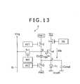
- FIG. 13is a schematic diagram illustrating the pixel circuit 2 in the display apparatus shown in FIG. 12 . Additionally written for easy understanding are a video signal Vsig sampled by the sampling transistor Tr 1 , the input voltage Vgs and output current Ids of the drive transistor Trd, and a capacity component Coled of the light emitting device EL. Three supply lines Vss 1 , Vss 2 , and Vcc are also added. Of the three power supplies, Vcc and Vss 2 are fixed power supplies. On the other hand, Vss 1 given to the gate G of the drive transistor Trd as a reference potential is a variable power supply. This variable power supply is made up of an external panel module, supplying reference potential Vss 1 to each pixel circuit 2 via wiring, this potential changing in level in a predetermined timed relation.
- FIG. 14is a timing chart of the pixel circuit shown in FIG. 13 .
- FIG. 14is indicative of waveforms of a control signal to be applied to the scan lines WS, AZ 1 , AZ 2 , and DS along time axis T.
- the control signalsare also denoted by the same reference notations as those of the scan lines. Since the sampling transistors Tr 1 , Tr 2 , and Tr 3 are of n-channel type, these transistors are turned on when the scan lines WS, AZ 1 , and AZ 2 go high and turned off when these scan lines go low.
- this transistor Tr 4is of p-channel type, this transistor is turned off when the scan line DS goes high and turned on when the scan line DS goes low. It should be noted that this timing chart also represent potential changes of the gate G and source S of the drive transistor Trd in addition to the waveforms of the control signals WS, AZ 1 , AZ 2 , and DS.
- timings T 1 to T 8provide one field ( 1 f). Each row of the pixel array is scanned once during one field. This timing chart is indicative of the waveforms of control signals WS, AZ 1 , AZ 2 , and DS to be applied to pixels for one row.
- control signals AZ 1 and AZ 2go high, so that the first switching transistor Tr 2 and the second switching transistor Tr 3 are turned on.
- the gate G of the drive transistor Trdis connected to the reference potential Vss 1 and the source S thereof is connected to the reference potential Vss 2 .
- Vss 1 ⁇ Vss 2Vth
- periods T 2 and T 3are equivalent to a reset period of the drive transistor Trd.
- the threshold voltage of the light emitting device ELbe VthEL, then VthEL>Vss 2 .
- the control signal AZ 2is turned low and, immediately thereafter, the control signal DS is turned low. Consequently, while the second switching transistor Tr 3 is turned off, the third switching transistor Tr 4 is turned on. As a result, the drain current Ids flows into the storage capacitor Cs, starting a Vth correcting operation. At this moment, the gate G of the drive transistor Trd is held at Vss 1 , in which the current Ids flows until the drive transistor Trd is cut off. When the drive transistor Trd is cut off, the source potential (S) of the drive transistor Trd becomes Vss 1 ⁇ Vth. In timing T 4 after the cutting off of the drain current, the control signal DS is turned high again, thereby turning off the third switching transistor Tr 4 .
- the control signal AZ 1is also turned low, also turning off the third switching transistor Tr 2 .
- Vthis fixed to the storage capacitor Cs.
- the timing T 3 and timing T 4provide periods in which the threshold voltage Vth of the drive transistor Trd is detected.
- the detection periods T 3 and T 4are referred to as Vth correction periods.
- the level of the reference potential Vss 1 applied to the gate G of the drive transistor Trdis switched low in timing T 4 . Consequently, the gate-to-source voltage Vgs of the drive transistor Trd can be compressed higher than a voltage equivalent to Vth. This compression fully turns off the drive transistor Trd, in which no leak current flows.
- the control signal AZ 1is switched from high to low to turn off the first switching transistor Tr 2 , upon which the gate G of the drive transistor Trd is disconnected from the reference potential Vss 1 , putting the drive transistor Trd into a floating state.
- the drive transistor TrdIn this floating state, the drive transistor Trd is fully off, so that no leak current flows, thereby maintaining the source voltage constantly.
- the threshold voltage Vth written to the storage capacitor Vgsis compressed by the level switching of the Vss 1 , which, however, does not cause the light emitting luminance fluctuation because the compression occurs commonly on all pixels. Conversely, the compression of Vgs prevents the leak current from flowing in the drive transistor Trd, thereby removing the influence by that fluctuation.
- the control signal WSis switched to high in timing T 5 to turn on the sampling transistor Tr 1 , thereby writing the video signal Vsig to the storage capacitor Cs.
- the storage capacitor Csis small enough.
- most part of the video signal Vsigis written to the storage capacitor Cs.
- difference between Vss 1 and Vsignamely, Vsig ⁇ Vss 1
- Vsig ⁇ Vss 1is written to the storage capacitor Cs. Therefore, the voltage Vgs between the gate G and source S of the drive transistor Trd becomes a level (Vsig ⁇ Vss 1 +Vth) obtained by adding Vth detected and stored last and Vsig ⁇ Vss 1 sampled this time.
- timings T 5 and T 6are equivalent to signal write periods.
- timing T 7the control signal DS goes low, turning on the third switching transistor Tr 4 . Consequently, the drive transistor Trd is connected to the power supply Vcc, so that the pixel circuit goes from the non-light emitting period to a light emitting period.
- the control signal WSwent low, so that the sampling transistor Tr 1 has already been turned off. Hence, the gate G of the drive transistor Trd is disconnected from the signal line SL. Because the application of the video signal Vsig has been cleared, the gate potential (G) of the drive transistor Trd can rise upon turning on of the third switching transistor Tr 4 , thereby rising along with the source potential (S).
- the source of the drive transistor Trdis connected to the anode of the light emitting device EL.
- the source potential (S) of the drive transistor Trdis also the anode potential Va of the light emitting device EL at the same time.
- the timing chart shown in FIG. 14is also indicative of the anode potential Va of the light emitting device EL. This light emitting period ends in timing T 8 before a next field.
- the gate potential (G) of the drive transistor Trdbecomes ready for rising and the source potential (S) rises in association therewith.
- Thisis a bootstrap operation.
- the gate-to-source voltage Vgs held in the storage capacitor Csmaintains a value (Vsig+Vth). Namely, this bootstrap operation permits the rise of the anode potential Va of the light emitting device EL while constantly maintaining the Vgs held in the storage capacitor Cs.
- k(1/2)(W/L)Cox (where W denotes transistor's gate width, L denotes gate length, and Cox denotes gate capacity).
- Wdenotes transistor's gate width
- Ldenotes gate length
- Coxdenotes gate capacity
- FIG. 15schematically shows a cross sectional structure of a pixel formed on an insulating substrate.
- the pixelhas a transistor section (in the figure, one TFT is shown for example) including a plurality of thin-film transistors, a capacitor section made up of a storage capacitor for example, and a light emitting section made up of an organic light emitting device EL for example.
- the transistor section and the capacitor sectionare formed on the substrate by a TFT process, over which the light emitting section, such as an light emitting device EL, is laminated. Over this laminated light emitting section, a transparent facing substrate is attached with an adhesive, thereby providing a flat panel.
- the display apparatusincludes a flat-type module-shaped display apparatus as shown in FIG. 16 .
- the display apparatus shown in FIG. 16has a pixel array section in which pixels each made up of an organic light emitting device EL, a thin-film transistor, and a thin-film capacitor are integratedly formed on an insulating substrate in a form of matrix. Adhesives are arranged around this pixel array section (or pixel matrix section) on which the facing substrate made up of glass for example is attached, thereby providing a display module.
- This transparent facing substratemay be arranged with a color filter, a protective film, and a light blocking film, for example, as required.
- the display modulemay be arranged with a FPC (Flexible Printed Circuit) for example as a connector through which signals or the like are transferred between the pixel array section and the outside.
- FPCFlexible Printed Circuit
- the above-described display apparatus according to the present embodimenthaving a flat panel shape, is applicable to displays of electronic devices of any fields that are configured to display drive signals supplied from the outside or generated inside these electronic devices as images or video.
- These electronic devicesinclude digital cameras, laptop personal computers, mobile phones, and video cameras, for example. The following describes some of these electronic devices to which the display apparatus according to the present embodiment is applied.
- FIG. 17shows a television set to which the display apparatus according to the present embodiment is applied.
- This television sethas a video display screen 11 made up of a front panel 12 and a filter glass 13 , for example, and is manufactured by use of the display apparatus according to the present embodiment as the video display screen 11 .
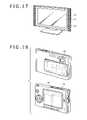
- FIG. 18shows a digital camera to which the display apparatus according to the present embodiment is applied.
- the topshows the front view of the digital camera, while the bottom shows the rear view.
- This digital camerahas a taking lens, a light emitting section 15 for flashing, a display section 16 , a control switch, a menu switch, and a shutter 19 , for example, and is manufactured by use of the display apparatus according to the present embodiment as the display section 16 .
- FIG. 19shows a laptop personal computer to which the display apparatus according to the present embodiment is applied.
- a main body 20has a keyboard 21 through which a user enters characters and so on into this personal computer.
- a main body cover of this personal computerhas a display section 22 for displaying images.
- This display section 22is made up of the display apparatus according to the present embodiment.
- FIG. 20shows a portable terminal device to which the display apparatus according to the present embodiment is applied. Shown to the left is the portable terminal device in an opened state. Shown to the right is the portable terminal device in a closed state.
- This portable terminal devicehas an upper housing 23 , a lower housing 24 , a link section (or hinge) 25 , a display 26 , a sub display 27 , a picture light 28 , a camera 29 and so on, for example.
- This portable terminal deviceis manufactured by applying the display apparatus according to the present embodiment to the display 26 and the sub display 27 .
- FIG. 21shows is a video camera to which the display apparatus according to the present embodiment is applied.
- This video camerahas a main body section 30 , a taking lens 34 for shooting an image-pickup object facing in front, a start/stop switch 35 for shooting, and a monitor 36 , for example.
- This video camerais manufactured by applying the display apparatus according to the present embodiment to the monitor 36 .
Landscapes
- Engineering & Computer Science (AREA)
- Physics & Mathematics (AREA)
- General Physics & Mathematics (AREA)
- Computer Hardware Design (AREA)
- Theoretical Computer Science (AREA)
- Nonlinear Science (AREA)
- Chemical & Material Sciences (AREA)
- Crystallography & Structural Chemistry (AREA)
- Mathematical Physics (AREA)
- Optics & Photonics (AREA)
- Control Of Indicators Other Than Cathode Ray Tubes (AREA)
- Control Of El Displays (AREA)
- Electroluminescent Light Sources (AREA)
Abstract
Description
- The present invention contains subject matter related to Japanese Patent Application JP 2007-074985 filed in the Japan Patent Office on Mar. 22, 2007, the entire contents of which being incorporated herein by reference.
- 1. Filed of the Invention
- The present invention relates to a display apparatus of active matrix type based on light emitting devices used as pixels and the drive method thereof. The present invention also relates to an electronic device based on this display apparatus.
- 2. Description of the Related Art
- Recently, planar self-luminous display apparatuses based on organic EL (ElectroLuminescence) devices have been increasingly under development. The organic EL device is a light emitting device based on a phenomenon in which light is emitted when an electric field is impressed upon an organic thin film. The organic EL device can be driven on less than10 V of applied voltage, so that this device involves low power dissipation. In addition, the organic EL device is self-luminous, so that no lighting member is required, thereby making this device light in weight and low in profile. Further, the response speed of the organic EL device is as fast as several microseconds, thereby suppressing the generation of afterimage at displaying a moving image.
- Of the planar self-luminous display apparatuses based on organic EL devices, most active is the development of active matrix display apparatuses with a thin-film transistor integratedly formed on each pixel. Active matrix planar self-luminous display apparatuses are disclosed in Japanese Patent Laid-Open No. 2003-255856, Japanese Patent Laid-Open No. 2003-271095, Japanese Patent Laid-Open No. 2004-133240, Japanese Patent Laid-Open No. 2004-029791, and Japanese Patent Laid-Open No. 2004-093682, for example (referred to as
Patent Documents 1 to 5 hereinafter). - However, related-art active matrix planar self-luminous display apparatuses involve a problem of causing the threshold voltage of the transistor for driving light emitting devices to fluctuate due to process variation. This characteristic fluctuation adversely affects light emitting luminance. Therefore, in order to uniformly control the light emitting luminance over the entire screen of the display apparatus, it is required to correct the threshold voltage fluctuation of the above-mentioned drive transistor in each pixel circuit. A display apparatus having such a threshold voltage correction capability for each pixel has been proposed.
- With related-art pixel circuits, a video signal with the threshold voltage corrected is sampled and the light emitting device is driven on the basis of the sampling. However, a current leak occurs on the drive transistor between the threshold voltage correcting operation and the light emitting operation, which causes the threshold voltage correction to be not necessarily executed correctly, thereby involving an error. This error or fluctuation of the threshold voltage correction causes the unevenness in light emitting luminance, which in turn causes impaired picture quality.
- Therefore, the present invention addresses the above-identified and other problems associated with related-art methods and apparatuses and solves the addressed problems by providing a display apparatus improved in the accuracy of a threshold voltage correcting operation by suppressing a current leak of a drive transistor to minimize the fluctuation of light emitting luminance. In carrying out the invention and according to a first embodiment thereof, there is provided a display apparatus. This display apparatus is made up of a pixel array section and a drive section, the pixel array section having power supply lines, scan lines arranged in row, signal lines arranged in column, and pixels arranged in matrix at intersections of each of the scan lines and each of the signal lines, each of the pixels at least having a sampling transistor, a drive transistor, a light emitting device, and a capacitor. The sampling transistor is connected at a control terminal thereof to the scan line and at one of a pair of current terminals of the sampling transistor to the scan line and at the other of the pair of current terminals to a control terminal of the drive transistor. The drive transistor is connected at one of a pair of current terminals to the light emitting device and at the other of the pair of current terminals to the power supply line. The drive section supplies a control signal to each scan line and a video signal to each signal line to drive each pixel, thereby executing a threshold voltage correcting operation for correcting a fluctuation of a threshold voltage of the drive transistor, a write operation for writing the video signal to the capacitor, and a light emitting operation for driving the light emitting device in accordance with the written video signal. The threshold voltage correcting operation has a preparation process in which, while the control terminal that is a gate of the drive transistor is maintained at a reference potential, a gate-to-source voltage with the current terminal that is a source of the drive transistor is set higher than the threshold voltage to turn on the drive transistor, an energizing process in which the drive transistor is energized with the gate maintained at the reference potential to hold, in the capacitor, a voltage equivalent to the threshold voltage appearing between the gate and the source when the drive transistor is cut off, and a compression process in which the reference potential applied to the gate is varied to compress the gate-to-source voltage to higher level than the voltage equivalent to the threshold voltage to surely turn off the drive transistor.
- In the above-mention first embodiment of the invention, the drive section has a write scanner for sequentially supplying control signals to scan lines for each horizontal scan period, a power supply scanner for switching each power supply line between high potential and low potential, and a signal driver for supplying a video signal in which a signal potential and a reference potential are switched in each horizontal scan period to each signal line. In the preparation period, while the write scanner outputs a control signal to turn on the sampling transistor and samples the reference potential from the signal line to apply the sampled reference potential to the gate of the drive transistor, the power supply scanner switches the power supply line from high potential to low potential to lower a potential of the source of the drive transistor to low potential. In the energizing process, the power supply scanner switches the power supply line from low potential to high potential to energize the drive transistor until the drive transistor cuts off. In the compression process, the signal driver switches a level of the reference potential downward immediately before the write scanner clears the control signal to turn off the sampling transistor while the power supply scanner maintains the power supply line at high potential.
- In carrying out the invention and according to a second embodiment thereof, there is provided a display apparatus. This display apparatus is made up of a pixel array section and a drive section. The pixel array section has power supply lines, scan lines arranged in row, signal lines arranged in column, and pixels arranged in matrix at intersections of each of the scan lines and each of the signal lines. Each of the pixels at least has a sampling transistor, a drive transistor, a light emitting device, and a capacitor. The sampling transistor is connected at a control terminal thereof to the scan line and at one of a pair of current terminals of the sampling transistor to the scan line and at the other of the pair of current terminals to a control terminal of the drive transistor. The drive transistor is connected at one of a pair of current terminals to the light emitting device and at the other of the pair of current terminals to the power supply line. The drive section supplies a control signal to each scan line and a video signal to each signal line to drive each pixel, thereby executing a threshold voltage correcting operation for correcting a fluctuation of a threshold voltage of the drive transistor, a write operation for writing the video signal to the capacitor, and a light emitting operation for emitting the light emitting device in accordance with the written video signal. The threshold voltage correcting operation has a preparation process in which, while the control terminal that is a gate of the drive transistor is maintained at a reference potential, a gate-to-source voltage with the current terminal that is a source of the drive transistor is set higher than the threshold voltage to turn on the drive transistor and an energizing process in which the drive transistor is energized with the gate maintained at the reference potential to hold, in the capacitor, a voltage equivalent to the threshold voltage appearing between the gate and the source when the drive transistor is cut off. The energizing process is executed in a time division manner a plurality of times until the drive transistor cuts off, there being a difference between a reference potential to be applied to the gate of the drive transistor in a preceding energizing process and a reference potential to be applied to the gate of the drive transistor in a following energizing process.
- Preferably, the energizing process is executed in a time division manner a plurality of times until the drive transistor cuts off and the reference potential to be applied to the gate of the drive transistor in the following energizing process becomes higher than the reference potential to be applied to the gate of the drive transistor in the preceding energizing process. The drive section has a write scanner for sequentially supplying control signals to scan lines for each horizontal scan period, a power supply scanner for switching each power supply line between high potential and low potential, and a signal driver for supplying a video signal in which a signal potential and a reference potential are switched in each horizontal scan period to each signal line; in the preparation period, while the write scanner outputs a control signal to turn on the sampling transistor and samples the reference potential from the signal line to apply the sampled reference potential to the gate of the drive transistor, the power supply scanner switches the power supply line from low potential to high potential to lower a potential of the source of the drive transistor to low potential; and in the energizing process, the power supply scanner switches the power supply line from high potential to low potential to energize the drive transistor until the drive transistor cuts off. The signal driver executes switching control such that the reference potential to be outputted to the signal line in the following energizing processing is higher than the reference potential to be outputted to the signal line in the preceding energizing process.
- With the display apparatus according to the present embodiment, each pixel executes a drive transistor threshold voltage correcting operation before executing a video signal write operation and a light emitting device lighting operation. This threshold voltage correcting operation includes a preparation process and an energizing process. In the preparation process, while he gate of the drive transistor is maintained at the reference potential, the gate-to-source voltage of the drive transistor is set higher than the threshold voltage to turn on the drive transistor. In the following energizing process, the drive transistor is energized with the gate maintained at the reference potential and, when the drive transistor cuts off, a voltage equivalent to the threshold voltage appearing between gate and source is held in the capacitor.
- According to the first embodiment of the invention, the threshold voltage correcting operation has a compression process after the above-mentioned preparation process and energizing process. In the compression process, the reference potential applied to the gate after the energizing process is varied to compress the gate-to-source voltage higher than the voltage equivalent to the threshold voltage, thereby surely turning off the drive transistor. This configuration prevents a leak current from flowing in the drive transistor, thereby stably maintaining results of the threshold voltage correcting operation until later write and light emitting operations. In other words, the fluctuation of the threshold voltage correcting operation is minimized to significantly enhance the accuracy. Consequently, the light emitting luminance has little fluctuation to significantly enhance the quality of screen.
- According to the second embodiment of the invention, the energizing process of the threshold voltage correcting operation is executed in a time division manner a plurality of times until the drive transistor is cut off. This configuration can give a sufficient energizing time, thereby surely allocating a voltage equivalent to the threshold voltage into the capacitor. In doing so, a difference is provided in the reference voltage level to be applied to the gate of the drive transistor between the preceding energizing process and the following energizing process. To be more specific, the reference voltage to be applied to the gate of the drive transistor in the following energizing process is set higher than that in the preceding energizing process. Thus, switching between the reference voltage levels in the energizing process executed in a time division manner can suppress the current leak of the drive transistor, eventually stabilizing the threshold voltage correcting operation and enhancing the accuracy thereof. Consequently, the fluctuation of the light emitting luminance of each pixel is minimized to improve the uniformity of screen.
FIG. 1 is a block diagram illustrating an overall configuration of a display apparatus practiced as one embodiment of the invention;FIG. 2 is a circuit diagram illustrating an exemplary configuration of a pixel included in the display apparatus shown inFIG. 1 ;FIG. 3 is a timing chart indicative of an operation of the display apparatus shown inFIGS. 1 and 2 ;FIG. 4 is a timing chart indicative of another operation of the above-mentioned display apparatus;FIG. 5 is a timing chart indicative of a still another operation of the above-mentioned display apparatus;FIG. 6 is a circuit diagram illustrating an exemplary configuration of a horizontal sector (or a signal driver) included in the display apparatus shown inFIGS. 1 and 2 ;FIG. 7 is a timing chart indicative of an operation of the signal driver shown inFIG. 6 ;FIG. 8 is a timing chart indicative of another operation of the above-mentioned signal driver;FIG. 9 is a timing chart indicative of an operation of the display apparatus shown inFIGS. 1 and 2 ;FIG. 10 is a timing chart indicative of another operation of the display apparatus shown inFIGS. 1 and 2 ;FIG. 11 is an overall block diagram illustrating a display apparatus practiced as another embodiment of the invention;FIG. 12 is a circuit diagram illustrating an exemplary configuration of a pixel included in the display apparatus shown inFIG. 11 ;FIG. 13 is a circuit diagram illustrating an exemplary configuration of the pixel;FIG. 14 is a timing chart indicative of an operation of the display apparatus shown inFIG. 11 ;FIG. 15 is a cross section illustrating a device configuration of the above-mentioned display apparatus;FIG. 16 is a top view illustrating a module configuration of the above-mentioned display apparatus;FIG. 17 is a perspective view illustrating a television set having the above-mentioned display apparatus;FIG. 18 is a perspective view illustrating a digital still camera having the above-mentioned display apparatus;FIG. 19 is a perspective view illustrating a note-type personal computer having the above-mentioned display apparatus;FIG. 20 is a schematic diagram illustrating a portable terminal apparatus having the above-mentioned display apparatus; andFIG. 21 is a perspective view illustrating a video camera having the above-mentioned display apparatus.- This invention will be described in further detail by way of embodiments thereof with reference to the accompanying drawings. Now, referring to
FIG. 1 , there is shown an overall configuration of a display apparatus practiced as one embodiment of the invention. As shown, the display apparatus is made up of apixel array block 1 and a drive block configured to drive thepixel array block 1. Thepixel array block 1 has write scan lines WS arranged in row, signal lines SL arranged in column,pixels 2 each arranged in row at each intersection between the write scan line WS and the signal lines SL, and power supply lines DS each arranged for each row ofpixels 2. The drive block has awrite scanner 4 for sequentially supplying control signals to the write scan lines to sequentially scanningpixels 2 on a row basis, adrive scanner 5 for supplying a supply voltage switching between high and low potentials for each power supply line DS in synchronization with this line sequential scan, and ahorizontal selector 3 for supplying a signal potential providing a video signal and a reference potential to each of signal lines SL arranged in column in synchronization with this line sequential scan. Thewrite scanner 4 and thedrive scanner 5 make up a scanner block and thehorizontal selector 3 makes up a signal driver. - Each
pixel 2 is made up of a sampling transistor Tr1, a drive transistor Trd, a storage capacitor (Cs), a sub capacitor (Csub), and a light emitting device EL. Each light emitting device EL is designed to emit light in one of three primary colors RGB. A pixel trio is made up of a pixel (RED) having a red light emitting device, a pixel (GREEN) having a green light emitting device, and a pixel (BLUE) having a blue light emitting device. Arranging pixel trios on thepixel array block 1 in a matrix allows color display. FIG. 2 shows a specific configuration of thepixel 2 included in the display apparatus shown inFIG. 1 and a line connection relationship of thepixel 2. As shown, thispixel 2 includes a light emitting device EL represented by an organic EL device for example, a sampling transistor Tr1, a drive transistor Trd, and a storage capacitor Cs. The sampling transistor Tr1 is connected at a gate thereof to the write scan line WS, at one of the source and drain thereof to a corresponding signal line SL, and at the other of the source and drain thereof to a gate G of the drive transistor Trd. The drive transistor Trd is connected at a source S thereof to the light emitting device EL, and at a drain thereof to a corresponding power supply line DS. A cathode of the light emitting device EL is connected to a ground potential Vcath. This ground wiring is common to allpixels 2. The storage capacitor (or a pixel capacitor) Cs is connected between the source S and the gate G of the drive transistor Trd. In addition, the sub capacitor Csub is connected in parallel to the light emitting device EL. This sub capacitor Csub, added as required, has a function of increasing an input gain of a video signal Vsig for the storage capacitor Cs.- The pixel configuration shown in
FIG. 2 is illustrative only and therefore the present invention is not restricted to this configuration. Basically, eachpixel 2 includes at least a sampling transistor Tr1, a drive transistor Trd, a light emitting device EL, and a storage capacitor Cs. The sampling transistor Tr1 is connected at a control terminal (or a gate) thereof to the write scan line WS and at a pair of current terminals (source and drain) thereof connected between the signal line SL and the control terminal of the drive transistor Trd. The drive transistor Trd is connected at one of the pair of current terminals (source and drain) to the light emitting device EL and at the other of the pair to the power supply line DS. The storage capacitor Cs is connected between the control terminal (gate G) of the drive transistor Trd and one (source S) of a pair of current terminals (source and drain) of the drive transistor Trd. FIG. 3 shows a timing chart indicative of an operation of thepixel 2 shown inFIG. 2 . It should be noted that this timing chart is not indicative of one embodiment of the invention, but is a first reference example indicative of an ideal operation status. This timing chart represents a potential change of scan line WS, a potential change of power supply line DS, and a potential change of signal line SL with reference to a common time axis. In parallel to these potential changes, changes of the gate G and the source S of the drive transistor Trd are also indicated.- In this timing chart, periods (0) to (7) are provided in match with operational transitions of the
pixel 2. First, in the light emitting period (0), the power supply line DS is at high potential Vccp and the drive transistor Trd is supplying drive current Ids to the light emitting device EL. Drive current Ids flows from the power supply line DS that is at high potential Vccp into common ground line Vcath through the light emitting device EL via the drive transistor Trd. - Next, in period (1), the power supply line DS is switched from high potential Vccp to low potential Vini. This discharges the power supply line DS to Vini and the source potential of the drive transistor Trd goes up to a potential near Vini. If the wiring capacity of the power supply line DS is relatively large, it is a good practice to switch the power supply line DS from high potential Vccp to low potential Vini as comparatively early as possible.
- In period (2), when the scan line WS is changed from low level to high level, the sampling transistor Tr1 gets in a conduction state. At this moment, the signal line SL is at reference voltage Vofs. Therefore, the gate potential of the drive transistor Trd provides reference potential Vofs of the signal line SL through the conductive sampling transistor Tr1. At the same time, the source potential of the drive transistor Trd is fixed to low potential Vini. Consequently, the source potential of the drive transistor Trd is reset to potential Vini that is lower enough than reference voltage Vofs of the signal line SL. To be more specific, low potential Vini of the power supply line DS is set so as to make a potential between gate and source (or a difference between gate potential and source potential) of the drive transistor Trd greater than threshold voltage Vth of the drive transistor Trd.
- As seen from the above description, period (1) and period (2) provide the preparatory processes for a threshold voltage correcting operation. Namely, in this preparatory process, while the control terminal that is the gate G of the drive transistor Trd is held at reference voltage Vofs, gate-to-source voltage Vgs between the current terminals that provide the source S of the drive transistor Trd is set higher than threshold voltage Vth, thereby turning on the drive transistor Trd.
- Next, in the Vth cancel period (3), the power supply line DS shifts from low potential ini to high potential Vccp, upon which the source potential of the drive transistor Trd starts rising. When the gate/source voltage Vgs of the drive transistor Trd has reached threshold voltage Vth, the current is cut off. Thus, a voltage equivalent to the threshold voltage Vth of the drive transistor Trd is written to the storage capacitor (pixel capacitor) Cs. This is a threshold voltage correcting operation. At this moment, in order to make the current solely flow to the storage capacitor Cs side and not the light emitting device EL side, the potential of common ground line Vcath is set in advance so as to cut off the light emitting device EL.
- As seen from the above description, this Vth cancel period (3) provides the energizing process of a threshold voltage correcting operation. In this energizing process, the drive transistor Trd is energized with the gate G held at reference potential Vofs and, when the drive transistor Trd is cut off, a voltage equivalent to the threshold voltage appearing between the gate and source of the drive transistor Trd is held in the storage capacitor Cs.
- Next, in the period (4), the scan line WS shifts to the low potential size, upon which the sampling transistor Tr1 goes off. At this moment, the gate G of the drive transistor Trd floats, but the gate-to-source voltage Vgs is in a cut off state because the gate-to-source voltage Vgs is equal to the threshold voltage Vth of the drive transistor Trd, no drain current Ids flowing. However, this is an ideal state; actually, because the drive transistor Trd involves a current leak, the drain current Ids flows even though small. Consequently, the source potential of the drive transistor Trd fluctuates, thereby causing the potential of the floating gate G to fluctuate, which is referred to as a bootstrap phenomenon.
- Next, in the period (5), the potential of the signal line SL changes from reference voltage Vofs to sampling potential (signal potential) Vsig. Consequently, preparations become ready for a next sampling operation and mobility correcting operation (signal write and mobility μ cancel).
- Then, in the signal write/mobility μ cancel period (6), the scan line WS shifts to the high potential side, upon which the sampling transistor Tr1 is turned on. Therefore, the gate potential of the drive transistor Trd becomes signal potential Vsig. Since the light emitting device EL is in the cut off state (a high impedance state) beforehand, the drain-to-source current Ids of the drive transistor Trd flows into the light emitting device capacitor and the sub capacitor Csub, starting charging these capacitors. Therefore, the source potential of the drive transistor Trd starts rising and the gate-to-source voltage Vgs of the drive transistor Trd gradually becomes Vsig+Vth−ΔV. Thus, the sampling of signal potential Vsig and the adjustment of correction amount ΔV are executed at the same time. As Vsig increases, Ids increases and also the absolute value of ΔV. Therefore, the mobility correction in accordance with light emitting luminance level is executed. If Vsig is constant, as the mobility μ of the drive transistor Trd increases, the absolute value of ΔV increases. In other words, as the mobility μ increases, negative feedback ΔV increases, so that the fluctuation of the mobility μ for each pixel can be removed.
- Last, in the light emitting period (7), the scan line WS shifts to the low potential side, upon which the sampling transistor Tr1 is turned off. Consequently, the gate G of the drive transistor Trd is disconnected from the signal line SL. At the same time, the drain current Ids starts flowing in the light emitting device EL. This raises the anode potential of the light emitting device EL in accordance with the drive current Ids. The rise of the anode potential of the light emitting device EL is nothing but the use of the source potential of the drive transistor Trd. When the source potential of the drive transistor Trd rises, the gate potential of the drive transistor Trd also rises by the bootstrap operation of the storage capacitor Cs. The amount of rise of the gate potential becomes equal to the amount of rise of the source potential. Therefore, the gate-to-source voltage Vgs of the drive transistor Trd during the light emitting period (7) is held at a constant level of Vsig+Vth−ΔV. It should be noted that, in the above description, Vgs is computed with Vofs=Vcath=0 V.
FIG. 4 is a timing chart indicative of an operation of the display apparatus shown inFIGS. 1 and 2 . This timing chart is representative of the actual potential changes of gate G and source S deviated from an ideal state providing a second reference example. For easy understanding, the same notation as that of the first reference example shown inFIG. 3 is used. As shown, in the second reference example indicative of an actual operation as with the first reference example, after an energizing process in the Vth cancel period (3), the scan line WS is lowered to turn off the sampling transistor Tr1. This temporarily disconnects the gate G of the drive transistor Trd from the signal line, thereby getting in a floating state. At this moment, switching of the sampling transistor Tr1 couples the gate G, thereby fluctuating the potential of the gate G. Accordingly, the potential of source S fluctuates. In addition, since there is a fluctuation in the characteristics of the drive transistor Trd of each pixel, a leak current flows between the drain and source of the drive transistor Trd. Affected by this leak, the source potential rises in the floating period (4). This causes the potential of the gate G to rise, too. This indicates that the same phenomenon as so-called bootstrap is taking place in this floating period (4).- Then, in the write period (6), the control signal is applied to the scan line WS again to turn on the sampling transistor Tr1, thereby writing signal potential Vsig to the gate G of the drive transistor Trd. At this moment, the potential of source S has slightly risen, so that the potential is a source potential indicated by X at the time when the write period (6) has ended. Since the source potential S and the gate potential G have risen during the floating period (4) because of the leak, the source potential S at the time when the write period (6) has ended is not necessarily constant, being different from a pixel to another. Hence, when the write period (6) has been completed, the source-to-gate voltage Vgs of the drive transistor Trd fluctuates between pixels, causing a difference in light emitting luminance. Generally, the trend of the leak of the drive transistor Trd appears along the scan line WS (line), so that the fluctuation of Vgs results in a horizontal irregularity of stripes at the time of emitting, thereby impairing screen uniformity. As the total number of pixels in the pixel array section increases caused by the increased resolution of display apparatuses, the horizontal scan period is shortened by that degree, the Vth cancel period (3) may not be sufficiently allocated. Therefore, the fluctuation of Vth of the drive transistor Trd may not be sufficiently canceled. If this state is further affected by the fluctuation of the leak of the drive transistor Trd, Vgs fluctuates to a large degree, thereby deteriorating the unevenness of stripes.
FIG. 5 shows a timing chart indicative of an operation of the display apparatus shown inFIGS. 1 and 2 . This timing chart is representative of one embodiment of the invention. For easy understanding, the same notations as those shown inFIGS. 3 and 4 are adopted. As shown, in the embodiment of the invention, after the energizing process of the Vth period (3) and before getting in the floating period (4), aperiod 3ais inserted, in which a compression process is executed. In this compression process, the reference potential Vofs applied to the gate G of the drive transistor Trd is altered to compress the gate-to-source voltage Vgs higher than the voltage equivalent to the threshold voltage Vth, thereby surely turning off the drive transistor Trd. To be more specific, in this compression process (3a), immediately before turning off the sampling transistor Tr1 by write scanner's clearing the control signal while maintaining the power supply line DS at the high potential Vccp, the signal driver downward switches the level of the reference potential Vofs from Vofs1 toVofs 2. Namely, immediately before the end of the Vth cancel period (3), the reference potential Vofs1 applied to the signal line SL is lowered to level Vofs2 at which Vth of the drive transistor Trd is cut in. Consequently, Vgs gets smaller than Vth, so that the current leak of the drive transistor Trd can be suppressed. As a result, the source potential of the drive transistor Trd will not fluctuate during the floating period (4), thereby suppressing the unevenness of light emitting luminance caused by the fluctuation of the leak current of the drive transistor.- It should be noted that, in lowering the signal line SL from the reference potential Vofs1 to Vofs2 in the compression process (3a), a drastic voltage variation may cause a coupling to the source S to open Vgs. In order to prevent this phenomenon, the transient may be smoothed to a degree at which no coupling takes place. The transient smoothing may be executed by blunting the rising edge of control signal pulse to be applied to the gate of the sampling transistor Tr1. For example, designing smaller the size of the N-channel transistor making up the last stage of the write scanner allows to blunt the rising edge of the gate pulse. Alternatively, the waveform of the reference potential Vofs with the falling edge blunted may be supplied to the power supply connected to the output buffer of the signal driver. Thus, in the present embodiment of the invention, in the reference potential write period (preparation period (2) and the Vth cancel period (3)) in which the sampling transistor Tr1 is turned on, the reference potential Vofs1 supplied from the signal line is applied to the gate G of the drive transistor Trd. In the final stage of this reference potential write period, the gate-to-source voltage Vgs of the drive transistor Trd is Vth. Immediately before the end of this reference potential write period, the reference potential Vofs1 is downward switched to Vofs2 to compress Vgs. Consequently, the drive transistor Trd is fully turned off, so that, in the floating period (4), no leak current flows, thereby making stable the potential of the source S of the drive transistor Trd.
- Then, in the signal potential write period (6), the control signal is applied to the scan line WS again, turning on the sampling transistor Tr1. At this point of time, the signal line SL has been switched to the signal potential Vsig, so that Vsig is written to the gate G of the drive transistor Trd. At this moment, part of the drain current Ids that flows in the drive transistor Trd is negatively fed back to the storage capacitor, so that the potential of source S of the drive transistor Trd rises to X as shown. Because the potential X is free from the influence of the leak, there is no fluctuation between pixels, thereby maintaining Vgs at a constant level to remove the unevenness in light emitting luminance.
FIG. 6 is a schematic circuit diagram illustrating an exemplary configuration of the horizontal selector (signal driver)3 included in the display apparatus shown inFIG. 1 . Thissignal driver 3 has a plurality of data lines Data1, Data2, and Data3, and so on and line-sequentially supplies data for one line to the signal lines SL arranged in column at the same time. In the example shown inFIG. 6 , one data line Data is connected with three signal lines SL via selector switches SEL1, SEL2, and SEL3, in which the signal potential supplied to one data line Data is supplied to the three signal lines SL in a time division manner.- A control line GOFS and a potential line VOFS are arranged in row, intersecting the signal lines SL arranged in column. The potential line VOFS is connected to each signal line SL with a switch SW. This switch SW is turned on/off by the control signal that is applied to the control line GOFS. A plurality of pixels connected to each signal line SL are each schematically represented by a capacitor C and a resistor R.
FIG. 7 is a timing chart indicative of an operation of the signal driver (or the horizontal selector)3 shown inFIG. 6 . The control signals to be applied to a set of three selector switches SEL1, SEL2, and SEL3 are represented by the same reference notations SEL1, SEL2, and SEL3. Likewise, the control signal to be applied to the control line GOFS is represented by the same reference notation GOFS. The potential of the potential line VOFS is fixed to Vofs2. Further, thesignal driver 3 has240 data lines, data (or signal potentials) to be applied these data lines being represented by Data1 toData 240. In addition, although not directly related with the operation of thesignal driver 3, timing signals WSEN1 and WSEN2 for controlling an operation of the write scanner side are represented in the timing chart shown inFIG. 7 as arranged along the time axis. The timing signal WSEN1 specifies the reference potential write period shown inFIG. 5 . The timing signal WSEN2 specifies the signal write period shown inFIG. 5 .- The timing signal WSEN1 goes high to get in the reference potential write period. At this moment, the potential to be applied to each data line Data is switched from the signal potential to the reference potential Vofs1. At the same time, the select signal SEL1, SEL2, and SEL3 go high simultaneously. These selector switches SEL1, SEL2, and SEL3 go on simultaneously to output the reference potential Vofs1 applied to the data line Data to the three signal lines SL. Therefore, during the reference potential write period, the reference potential Vofs1 is simultaneously written to the signal lines SL arranged in column.
- Then, immediately before the WSEN1 is switched from high to low, the control signal GOFS goes high, upon which the switches SW are simultaneously turned on. At this point of time, the
selector 1, theselector 2, and theselector 3 are in the off state. The potential Vofs2 of the potential line VOFS is written to each signal line SL via the switch SW. Thus, immediately before the end of the reference potential write period, the potential of each signal line SL is downward switched from Vofs1 to Vofs2, thereby realizing the above-mentioned Vgs compression process. - Thereafter, a predetermined signal potential is supplied to each data line Data. In synchronization therewith, the select signals SEL1, SEL2, and SEL3 go high in a time division manner, writing the corresponding signal potential to the corresponding signal lines SL. Next, when the timing signal WSEN2 goes high, the signal potential write period goes on, in which the sampling transistors of the pixels for one line are simultaneously turned on. This samples the signal potential applied to each signal line SL into the pixels for one line, executing a line-sequential write operation.
FIG. 8 is a timing chart indicative of a operation of thesignal driver 3 shown inFIG. 6 . It should be noted that this timing chart is representative of a reference example in which reference potential switching is not executed. As shown, in this reference example, while a signal potential is supplied to the data line Data, the reference potential Vofs is supplied to the potential line VOFS. When the timing signal WSEN1 goes high to get in the reference potential write period, the control signal GOFS goes high, upon which the switches SW are simultaneously turned on. Via these turned-on switches SW, the reference potential Vofs of the potential line VOFS is supplied to the signal lines SL arranged in column. As seen from the above description, the level switching of the reference potential Vofs is not executed in this reference example.FIG. 9 is a timing chart indicative of an operation of the display apparatus shown inFIGS. 1 and 2 . This timing chart is representative of a third reference example. For easy understanding, the same reference notation as that of the previous reference examples shown inFIGS. 3 and 4 is used. A difference lies in that, in the third reference example, the energizing process of a threshold voltage correcting operation is repeatedly executed several times in a time division manner. Generally, pixels threshold correcting operation, signal potential write operation, and light emitting operation are line-sequentially executed for each line. Therefore, a threshold voltage correcting operation is also executed, one horizontal scan period (1H) for each line. However, as the pixel definition goes higher, the number of scan lines increases, so that the H period is shortened by that amount, disabling to provide a sufficient Vth cancel period. Therefore, it may be executed the energizing process requiring time in a threshold voltage correcting operation over a plurality of horizontal periods in a time division manner as described in this reference example. The reference example shown inFIG. 9 shows a case in which the Vth cancel operation has been executed twice. The energizing process is executed in the first Vth cancel period (31); however, because the time is not long enough, Vgs has not reached Vth. When the first Vth cancel period (31) comes to an end, the control signal is once switched to the low level to turn off the sampling transistor Tr1, disconnecting the gate G of the drive transistor Trd from the signal line SL. Consequently, the gate G of the drive transistor Trd gets in a floating state. During this floating period (41), the drive transistor Trd is not off, therefore a leak current flows. Therefore, as the source potential S rises, the potential of the gate G rises in association therewith. This is a so-called bootstrap phenomenon. This current leak becomes large as the Vth cancel is insufficient in the first Vth cancel period (31). Consequently, at the time the floating period (41) ends, the source voltage of the drive transistor Trd largely fluctuates from pixel to pixel.- Next, in the second Vth cancel period (32), the control signal goes high again to execute the energizing process with Vofs applied to the gate G of the drive transistor Trd. This causes Vgs to reach Vth. Then, after getting in the floating period (42) again, the signal potential Vsig is written to the gate G of the drive transistor Trd in the signal potential write period (6) and, at the same time, the source potential also rises to a predetermined level. However, if the Vth cancel is insufficient in the first energizing process, a large fluctuation occurs in the current leak in the subsequent floating period (41) to adversely affect the second threshold correcting operation, thereby eventually leaving the Vgs fluctuation for each pixel at the time when the signal potential write period has ended. This remaining fluctuation is recognized as a stripe unevenness at the time of light emitting.
FIG. 10 is a timing chart indicative of an operation of the display apparatus shown inFIGS. 1 and 2 . This timing chart is represents a second embodiment of the invention that is configured to overcome the above-mentioned problems involved in the third reference examples shown inFIG. 9 . In this second embodiment, a threshold voltage correcting operation is executed in a time division manner; namely, the first energizing process (31) and the second energizing process (32) are executed with a time lag in between. One of characteristics of the present invention is that the reference potential Vofs1 used in the first Vth cancel period (31) and the reference potential Vofs2 used on the second Vth cancel period (32) are different from each other. To be more specific, in the first Vth cancel period (31), the reference potential Vofs1 to be applied to the gate G of the drive transistor Trd is lower than the reference potential Vofs2 to be written to the gate G in the second Vth correction period (32). Consequently, if the first Vth cancel period (31) had ended insufficiently, the current leak of the drive transistor Trd that is caused by Vgs's opening wide can be prevented or minimized by shrinking Vgs by setting Vofs1 in advance. Generally, executing the Vth cancel operation n times requires to set the Vofs to be used in the first Vth cancel to the lowest level and the Vofs to be used in the second and subsequent Vth cancels to higher levels sequentially or at least a level equal to the previous level. This technique can suppress the current leak that may occur during the floating period after the Vth cancel.FIG. 11 is a block diagram illustrating a display apparatus practiced as another embodiment of the invention. As shown, this display apparatus is basically made up of apixel array block 1, a scanner block, and a signal block. Thepixel array block 1 has a first scan line WS, a second scan line AZ1, a third scan line AZ2, and a fourth scan line DS that are arranged in row, signal lines SL arranged in column,pixel circuits 2 arranged in matrix connected to these scan lines WS, AZ1, AZ2, DS, and SL, and a plurality of power supply lines for supplying power a first potential Vss1, a second potential Vss2, and a third potential Vcc that are necessary for operations of thesepixel circuits 2. The signal block is made up of ahorizontal selector 3 that supplies video signals to the signal line SL. The scanner block is made up of awrite scanner 4, adrive scanner 5, afirst correction scanner 71, and asecond correction scanner 72, supplying controls signals to the first scan line WS, the fourth scan line DS, the second scan line AZ1, and the third scan line AZ2, respectively, thereby sequentially scanning the pixel circuits on a row basis.FIG. 12 is a circuit diagram illustrating an exemplary configuration of a pixel circuit to be built in the display apparatus shown inFIG. 11 . Apixel 2 shown inFIG. 12 has a sampling transistor Tr1, a drive transistor Trd, a first switching transistor Tr2, a second switching transistor Tr3, a third switching transistor Tr4, a storage capacitor Cs, and a light emitting device EL. The sampling transistor Tr1 conducts in accordance with a control signal supplied from the first scan line WS during a predetermined sampling period to sample the signal potential of a video signal supplied from the signal line SL into the storage capacitor Cs. The storage capacitor Cs applies an input voltage Vgs to the gate G of the drive transistor Trd in accordance with the signal potential of the sampled video signal. The drive transistor Trd supplies an output current Ids to the light emitting device EL in accordance with the input voltage Vgs. The light emitting device EL emits light at the luminance in accordance with the signal potential of the video signal by the output current Ids supplied from the drive transistor Trd during a predetermined light emitting period.- Before the sampling period, the first switching transistor Tr2 conducts in accordance with the control signal supplied from a second scan line AZ1 to set the gate G of the drive transistor Trd to a first potential Vss1. Before the sampling period, the second switching transistor Tr3 conducts in accordance with the control signal supplied from a third scan line AZ2 to set the source S of the drive transistor Trd to a second potential Vss2. Before the sampling period, the third switching transistor Tr4 conducts in accordance with the control signal supplied from a fourth scan line DS connects the drive transistor Trd to a third potential Vcc, thereby holding a voltage equivalent to threshold voltage Vth of the drive transistor Trd in the storage capacitor Cs, thereby correcting the influence of the threshold voltage Vth. Further, the third switching transistor Tr4 conducts again in accordance with the control signal supplied from the fourth scan line DS during the light emitting period to connect the drive transistor Trd to the third potential Vcc, thereby flowing the output current Ids to the light emitting device EL.
- As seen from the above description, the
pixel circuit 2 has five transistors Tr1 to Tr4, one drive transistor Trd, one storage capacitor Cs, and the light emitting device EL. The transistors Tr1 to Tr3 and the Trd are each an n-channel polysilicon TFT. Only the transistor Tr4 is a p-channel polysilicon TFT. However, the present invention is not restricted thereto; for example, n-channel and p-channel TFTs can coexist appropriately. The light emitting device EL is a diode-type organic EL device having anode and cathode, for example. However, the present invention is not restricted thereto; for example, the light emitting device in the present invention may include any device that emits light generally driven by electric current. FIG. 13 is a schematic diagram illustrating thepixel circuit 2 in the display apparatus shown inFIG. 12 . Additionally written for easy understanding are a video signal Vsig sampled by the sampling transistor Tr1, the input voltage Vgs and output current Ids of the drive transistor Trd, and a capacity component Coled of the light emitting device EL. Three supply lines Vss1, Vss2, and Vcc are also added. Of the three power supplies, Vcc and Vss2 are fixed power supplies. On the other hand, Vss1 given to the gate G of the drive transistor Trd as a reference potential is a variable power supply. This variable power supply is made up of an external panel module, supplying reference potential Vss1 to eachpixel circuit 2 via wiring, this potential changing in level in a predetermined timed relation.FIG. 14 is a timing chart of the pixel circuit shown inFIG. 13 . The following specifically describes an operation of the pixel circuit shown inFIG. 13 with reference toFIG. 14 .FIG. 14 is indicative of waveforms of a control signal to be applied to the scan lines WS, AZ1, AZ2, and DS along time axis T. For the brevity of notation, the control signals are also denoted by the same reference notations as those of the scan lines. Since the sampling transistors Tr1, Tr2, and Tr3 are of n-channel type, these transistors are turned on when the scan lines WS, AZ1, and AZ2 go high and turned off when these scan lines go low. On the other hand, since the third switching transistor Tr4 is of p-channel type, this transistor is turned off when the scan line DS goes high and turned on when the scan line DS goes low. It should be noted that this timing chart also represent potential changes of the gate G and source S of the drive transistor Trd in addition to the waveforms of the control signals WS, AZ1, AZ2, and DS.- In the timing chart shown in
FIG. 14 , timings T1 to T8 provide one field (1f). Each row of the pixel array is scanned once during one field. This timing chart is indicative of the waveforms of control signals WS, AZ1, AZ2, and DS to be applied to pixels for one row. - In timing To before a field concerned starts, all control signals WS, AZ1, AZ2, and DS are low. Therefore, while the n-channel type transistors Tr1, Tr2, and Tr3 are off, the p-channel type transistor Tr4 is on. Therefore, because the drive transistor Trd is connected to the power supply Vcc via the transistor Tr4 in the on state, the drive transistor Trd supplies an output current Ids to the light emitting device EL in accordance with a predetermined input voltage Vgs. Consequently, the light emitting device EL is emitting light in timing TO. At this moment, the input voltage Vgs to be applied to the drive transistor Trd is represented by a difference between gate potential (G) and source potential (S).
- In timing T1 at which the field concerned starts, the control signal DS changes from low to high. Consequently, the third switching transistor Tr4 is turned off to disconnect the drive transistor Trd from the power Vcc, so that light emitting stops to get in the non-light emitting period. Therefore, in timing T1, all transistors Tr1 to Tr4 are turned off.
- Next, in timing T2, control signals AZ1 and AZ2 go high, so that the first switching transistor Tr2 and the second switching transistor Tr3 are turned on. As a result, the gate G of the drive transistor Trd is connected to the reference potential Vss1 and the source S thereof is connected to the reference potential Vss2. Here, if Vss1−Vss2>Vth, where Vss1−Vss2=Vgs>Vth, then preparations for Vth correction to be executed in the subsequent timing T3 are executed. In other words, periods T2 and T3 are equivalent to a reset period of the drive transistor Trd. Let the threshold voltage of the light emitting device EL be VthEL, then VthEL>Vss2. Consequently, a minus bias is applied to the light emitting device EL, so that the light emitting device EL is put in a so-called reverse bias state. This reverse bias state is necessary to normally execute a Vth correcting operation and a mobility correcting operation to be executed later.
- In timing T3, the control signal AZ2 is turned low and, immediately thereafter, the control signal DS is turned low. Consequently, while the second switching transistor Tr3 is turned off, the third switching transistor Tr4 is turned on. As a result, the drain current Ids flows into the storage capacitor Cs, starting a Vth correcting operation. At this moment, the gate G of the drive transistor Trd is held at Vss1, in which the current Ids flows until the drive transistor Trd is cut off. When the drive transistor Trd is cut off, the source potential (S) of the drive transistor Trd becomes Vss1−Vth. In timing T4 after the cutting off of the drain current, the control signal DS is turned high again, thereby turning off the third switching transistor Tr4. Further, the control signal AZ1 is also turned low, also turning off the third switching transistor Tr2. As a result, Vth is fixed to the storage capacitor Cs. Thus, the timing T3 and timing T4 provide periods in which the threshold voltage Vth of the drive transistor Trd is detected. Here, the detection periods T3 and T4 are referred to as Vth correction periods.
- After detecting the threshold voltage Vth of the drive transistor Trd and writing the detected voltage to the storage capacitor Cs, the level of the reference potential Vss1 applied to the gate G of the drive transistor Trd is switched low in timing T4. Consequently, the gate-to-source voltage Vgs of the drive transistor Trd can be compressed higher than a voltage equivalent to Vth. This compression fully turns off the drive transistor Trd, in which no leak current flows. After this, the control signal AZ1 is switched from high to low to turn off the first switching transistor Tr2, upon which the gate G of the drive transistor Trd is disconnected from the reference potential Vss1, putting the drive transistor Trd into a floating state. In this floating state, the drive transistor Trd is fully off, so that no leak current flows, thereby maintaining the source voltage constantly. The threshold voltage Vth written to the storage capacitor Vgs is compressed by the level switching of the Vss1, which, however, does not cause the light emitting luminance fluctuation because the compression occurs commonly on all pixels. Conversely, the compression of Vgs prevents the leak current from flowing in the drive transistor Trd, thereby removing the influence by that fluctuation.
- After the correction of Vth as described above, the control signal WS is switched to high in timing T5 to turn on the sampling transistor Tr1, thereby writing the video signal Vsig to the storage capacitor Cs. As compared with the equivalent capacitor Coled of the light emitting device EL, the storage capacitor Cs is small enough. As a result, most part of the video signal Vsig is written to the storage capacitor Cs. To be correct, difference between Vss1 and Vsig, namely, Vsig−Vss1, is written to the storage capacitor Cs. Therefore, the voltage Vgs between the gate G and source S of the drive transistor Trd becomes a level (Vsig−Vss1+Vth) obtained by adding Vth detected and stored last and Vsig−Vss1 sampled this time. For the brevity of description, let Vss1=0 V, then the gate-to-source voltage Vgs becomes Vsig+Vth as indicated by the timing chart shown in
FIG. 4 . The sampling of the video signal Vsig is executed until timing T6 in which the control signal WS returns to the low level. Namely, timings T5 and T6 are equivalent to signal write periods. - Next, in timing T7, the control signal DS goes low, turning on the third switching transistor Tr4. Consequently, the drive transistor Trd is connected to the power supply Vcc, so that the pixel circuit goes from the non-light emitting period to a light emitting period. In the preceding timing T6, the control signal WS went low, so that the sampling transistor Tr1 has already been turned off. Hence, the gate G of the drive transistor Trd is disconnected from the signal line SL. Because the application of the video signal Vsig has been cleared, the gate potential (G) of the drive transistor Trd can rise upon turning on of the third switching transistor Tr4, thereby rising along with the source potential (S). It should be noted that, with the pixel circuit according to the present embodiment, the source of the drive transistor Trd is connected to the anode of the light emitting device EL. Hence, the source potential (S) of the drive transistor Trd is also the anode potential Va of the light emitting device EL at the same time. The timing chart shown in
FIG. 14 is also indicative of the anode potential Va of the light emitting device EL. This light emitting period ends in timing T8 before a next field. - As described above, in timing T7, the gate potential (G) of the drive transistor Trd becomes ready for rising and the source potential (S) rises in association therewith. This is a bootstrap operation. During this bootstrap operation, the gate-to-source voltage Vgs held in the storage capacitor Cs maintains a value (Vsig+Vth). Namely, this bootstrap operation permits the rise of the anode potential Va of the light emitting device EL while constantly maintaining the Vgs held in the storage capacitor Cs. As the source potential (S) of the drive transistor, namely, the anode potential Va of the light emitting device EL rises, the reserve bias state of the light emitting device EL is cleared, so that the inflow of output current Ids causes the light emitting device EL to actually start light emission. A relationship at this moment between the drain current Ids and the gate voltage Vgs is given by the following equation by substituting Vsig+Vth into the Vgs of the above-mentioned transistor characteristic equation 1:
Ids=k·μ(Vgs−Vth)2=Kμ(Vsig)2- In the above equation, k=(1/2)(W/L)Cox (where W denotes transistor's gate width, L denotes gate length, and Cox denotes gate capacity). This equation is indicative that the term of Vth is canceled and the output current Ids to be supplied to the light emitting device EL is not dependent on the threshold voltage Vth of the drive transistor Trd. Basically, the drain current Ids is determined by the signal voltage Vsig of a video signal. In other words, the light emitting device EL emits light with a luminance in accordance with the video signal Vsig. In addition, this pixel circuit according to the present embodiment constantly maintains the gate voltage Vgs independently of the source potential of the drive transistor, namely, the anode potential Va of the light emitting device. This bootstrap capability allows the screen luminance to be maintained with stability without being affected by the time-dependent variation of the I-V characteristic of the light emitting device EL.
- The display apparatus according to the present embodiment has a thin-film device configuration as shown in
FIG. 15 .FIG. 15 schematically shows a cross sectional structure of a pixel formed on an insulating substrate. As shown, the pixel has a transistor section (in the figure, one TFT is shown for example) including a plurality of thin-film transistors, a capacitor section made up of a storage capacitor for example, and a light emitting section made up of an organic light emitting device EL for example. The transistor section and the capacitor section are formed on the substrate by a TFT process, over which the light emitting section, such as an light emitting device EL, is laminated. Over this laminated light emitting section, a transparent facing substrate is attached with an adhesive, thereby providing a flat panel. - The display apparatus according to the present embodiment includes a flat-type module-shaped display apparatus as shown in
FIG. 16 . For example, the display apparatus shown inFIG. 16 has a pixel array section in which pixels each made up of an organic light emitting device EL, a thin-film transistor, and a thin-film capacitor are integratedly formed on an insulating substrate in a form of matrix. Adhesives are arranged around this pixel array section (or pixel matrix section) on which the facing substrate made up of glass for example is attached, thereby providing a display module. This transparent facing substrate may be arranged with a color filter, a protective film, and a light blocking film, for example, as required. The display module may be arranged with a FPC (Flexible Printed Circuit) for example as a connector through which signals or the like are transferred between the pixel array section and the outside. - The above-described display apparatus according to the present embodiment, having a flat panel shape, is applicable to displays of electronic devices of any fields that are configured to display drive signals supplied from the outside or generated inside these electronic devices as images or video. These electronic devices include digital cameras, laptop personal computers, mobile phones, and video cameras, for example. The following describes some of these electronic devices to which the display apparatus according to the present embodiment is applied.
FIG. 17 shows a television set to which the display apparatus according to the present embodiment is applied. This television set has avideo display screen 11 made up of afront panel 12 and afilter glass 13, for example, and is manufactured by use of the display apparatus according to the present embodiment as thevideo display screen 11.FIG. 18 shows a digital camera to which the display apparatus according to the present embodiment is applied. The top shows the front view of the digital camera, while the bottom shows the rear view. This digital camera has a taking lens, alight emitting section 15 for flashing, adisplay section 16, a control switch, a menu switch, and ashutter 19, for example, and is manufactured by use of the display apparatus according to the present embodiment as thedisplay section 16.FIG. 19 shows a laptop personal computer to which the display apparatus according to the present embodiment is applied. Amain body 20 has akeyboard 21 through which a user enters characters and so on into this personal computer. A main body cover of this personal computer has adisplay section 22 for displaying images. Thisdisplay section 22 is made up of the display apparatus according to the present embodiment.FIG. 20 shows a portable terminal device to which the display apparatus according to the present embodiment is applied. Shown to the left is the portable terminal device in an opened state. Shown to the right is the portable terminal device in a closed state. This portable terminal device has anupper housing 23, alower housing 24, a link section (or hinge)25, adisplay 26, asub display 27, a picture light28, acamera 29 and so on, for example. This portable terminal device is manufactured by applying the display apparatus according to the present embodiment to thedisplay 26 and thesub display 27.FIG. 21 shows is a video camera to which the display apparatus according to the present embodiment is applied. This video camera has amain body section 30, a takinglens 34 for shooting an image-pickup object facing in front, a start/stop switch 35 for shooting, and amonitor 36, for example. This video camera is manufactured by applying the display apparatus according to the present embodiment to themonitor 36.- While preferred embodiments of the present invention have been described using specific terms, such description is for illustrative purpose only, and it is to be understood that changes and variations may be made without departing from the spirit or scope of the following claims.
Claims (11)
Applications Claiming Priority (2)
| Application Number | Priority Date | Filing Date | Title |
|---|---|---|---|
| JP2007-074985 | 2007-03-22 | ||
| JP2007074985AJP4306753B2 (en) | 2007-03-22 | 2007-03-22 | Display device, driving method thereof, and electronic apparatus |
Publications (2)
| Publication Number | Publication Date |
|---|---|
| US20080231625A1true US20080231625A1 (en) | 2008-09-25 |
| US8836690B2 US8836690B2 (en) | 2014-09-16 |
Family
ID=39774223
Family Applications (1)
| Application Number | Title | Priority Date | Filing Date |
|---|---|---|---|
| US12/076,156Expired - Fee RelatedUS8836690B2 (en) | 2007-03-22 | 2008-03-14 | Display apparatus and drive method thereof and electronic device |
Country Status (5)
| Country | Link |
|---|---|
| US (1) | US8836690B2 (en) |
| JP (1) | JP4306753B2 (en) |
| KR (1) | KR20080086371A (en) |
| CN (1) | CN101271667B (en) |
| TW (1) | TW200901129A (en) |
Cited By (79)
| Publication number | Priority date | Publication date | Assignee | Title |
|---|---|---|---|---|
| US20090315812A1 (en)* | 2008-06-18 | 2009-12-24 | Sony Corporation | Panel and drive control method |
| US20100176400A1 (en)* | 2009-01-09 | 2010-07-15 | Sony Corporation | Display device and electronic apparatus |
| US20100245334A1 (en)* | 2009-03-25 | 2010-09-30 | Sony Corporation | Display apparatus and electronic instrument |
| US20100245324A1 (en)* | 2009-03-25 | 2010-09-30 | Sony Corporation | Display apparatus and electronic instrument |
| US20110001741A1 (en)* | 2009-07-02 | 2011-01-06 | Sony Corporation | Display device and electronic apparatus |
| US20110169872A1 (en)* | 2010-01-14 | 2011-07-14 | Sony Corporation | Display apparatus and display driving method |
| US20110181629A1 (en)* | 2010-01-28 | 2011-07-28 | Sony Corporation | Display device, method of driving the display device, and electronic device |
| US20110205205A1 (en)* | 2010-02-24 | 2011-08-25 | Sony Corporation | Pixel circuit, display device, method of driving the display device, and electronic unit |
| US20120081381A1 (en)* | 2010-09-30 | 2012-04-05 | Casio Computer Co., Ltd. | Display drive device, display device, driving control method, and electronic device |
| US20130300724A1 (en)* | 2012-05-11 | 2013-11-14 | Ignis Innovation Inc. | Pixel circuits including feedback capacitors and reset capacitors, and display systems therefore |
| US8994617B2 (en) | 2010-03-17 | 2015-03-31 | Ignis Innovation Inc. | Lifetime uniformity parameter extraction methods |
| US9059117B2 (en) | 2009-12-01 | 2015-06-16 | Ignis Innovation Inc. | High resolution pixel architecture |
| US9275579B2 (en) | 2004-12-15 | 2016-03-01 | Ignis Innovation Inc. | System and methods for extraction of threshold and mobility parameters in AMOLED displays |
| US9280933B2 (en) | 2004-12-15 | 2016-03-08 | Ignis Innovation Inc. | System and methods for extraction of threshold and mobility parameters in AMOLED displays |
| US9324268B2 (en) | 2013-03-15 | 2016-04-26 | Ignis Innovation Inc. | Amoled displays with multiple readout circuits |
| US9336717B2 (en) | 2012-12-11 | 2016-05-10 | Ignis Innovation Inc. | Pixel circuits for AMOLED displays |
| US9343006B2 (en) | 2012-02-03 | 2016-05-17 | Ignis Innovation Inc. | Driving system for active-matrix displays |
| US9355584B2 (en) | 2011-05-20 | 2016-05-31 | Ignis Innovation Inc. | System and methods for extraction of threshold and mobility parameters in AMOLED displays |
| US9418587B2 (en) | 2009-06-16 | 2016-08-16 | Ignis Innovation Inc. | Compensation technique for color shift in displays |
| US9437137B2 (en) | 2013-08-12 | 2016-09-06 | Ignis Innovation Inc. | Compensation accuracy |
| US9466240B2 (en) | 2011-05-26 | 2016-10-11 | Ignis Innovation Inc. | Adaptive feedback system for compensating for aging pixel areas with enhanced estimation speed |
| US9472139B2 (en) | 2003-09-23 | 2016-10-18 | Ignis Innovation Inc. | Circuit and method for driving an array of light emitting pixels |
| US9489897B2 (en) | 2010-12-02 | 2016-11-08 | Ignis Innovation Inc. | System and methods for thermal compensation in AMOLED displays |
| US9489891B2 (en) | 2006-01-09 | 2016-11-08 | Ignis Innovation Inc. | Method and system for driving an active matrix display circuit |
| US9530352B2 (en) | 2006-08-15 | 2016-12-27 | Ignis Innovations Inc. | OLED luminance degradation compensation |
| US9530349B2 (en) | 2011-05-20 | 2016-12-27 | Ignis Innovations Inc. | Charged-based compensation and parameter extraction in AMOLED displays |
| US9536460B2 (en) | 2012-05-23 | 2017-01-03 | Ignis Innovation Inc. | Display systems with compensation for line propagation delay |
| US9536465B2 (en) | 2013-03-14 | 2017-01-03 | Ignis Innovation Inc. | Re-interpolation with edge detection for extracting an aging pattern for AMOLED displays |
| US9633597B2 (en) | 2006-04-19 | 2017-04-25 | Ignis Innovation Inc. | Stable driving scheme for active matrix displays |
| US9697771B2 (en) | 2013-03-08 | 2017-07-04 | Ignis Innovation Inc. | Pixel circuits for AMOLED displays |
| US9721505B2 (en) | 2013-03-08 | 2017-08-01 | Ignis Innovation Inc. | Pixel circuits for AMOLED displays |
| US9741292B2 (en) | 2004-12-07 | 2017-08-22 | Ignis Innovation Inc. | Method and system for programming and driving active matrix light emitting device pixel having a controllable supply voltage |
| US9741282B2 (en) | 2013-12-06 | 2017-08-22 | Ignis Innovation Inc. | OLED display system and method |
| US9761170B2 (en) | 2013-12-06 | 2017-09-12 | Ignis Innovation Inc. | Correction for localized phenomena in an image array |
| US9773439B2 (en) | 2011-05-27 | 2017-09-26 | Ignis Innovation Inc. | Systems and methods for aging compensation in AMOLED displays |
| US20170278461A1 (en)* | 2014-08-22 | 2017-09-28 | Joled Inc. | Drive method for display device and display device |
| US9786223B2 (en) | 2012-12-11 | 2017-10-10 | Ignis Innovation Inc. | Pixel circuits for AMOLED displays |
| US9786209B2 (en) | 2009-11-30 | 2017-10-10 | Ignis Innovation Inc. | System and methods for aging compensation in AMOLED displays |
| US9824632B2 (en) | 2008-12-09 | 2017-11-21 | Ignis Innovation Inc. | Systems and method for fast compensation programming of pixels in a display |
| US9881532B2 (en) | 2010-02-04 | 2018-01-30 | Ignis Innovation Inc. | System and method for extracting correlation curves for an organic light emitting device |
| US9947293B2 (en) | 2015-05-27 | 2018-04-17 | Ignis Innovation Inc. | Systems and methods of reduced memory bandwidth compensation |
| US9970964B2 (en) | 2004-12-15 | 2018-05-15 | Ignis Innovation Inc. | Method and system for programming, calibrating and driving a light emitting device display |
| US10012678B2 (en) | 2004-12-15 | 2018-07-03 | Ignis Innovation Inc. | Method and system for programming, calibrating and/or compensating, and driving an LED display |
| US10013907B2 (en) | 2004-12-15 | 2018-07-03 | Ignis Innovation Inc. | Method and system for programming, calibrating and/or compensating, and driving an LED display |
| US10019941B2 (en) | 2005-09-13 | 2018-07-10 | Ignis Innovation Inc. | Compensation technique for luminance degradation in electro-luminance devices |
| US10032399B2 (en) | 2010-02-04 | 2018-07-24 | Ignis Innovation Inc. | System and methods for extracting correlation curves for an organic light emitting device |
| US10074304B2 (en) | 2015-08-07 | 2018-09-11 | Ignis Innovation Inc. | Systems and methods of pixel calibration based on improved reference values |
| US10089921B2 (en) | 2010-02-04 | 2018-10-02 | Ignis Innovation Inc. | System and methods for extracting correlation curves for an organic light emitting device |
| US10089924B2 (en) | 2011-11-29 | 2018-10-02 | Ignis Innovation Inc. | Structural and low-frequency non-uniformity compensation |
| US10102808B2 (en) | 2015-10-14 | 2018-10-16 | Ignis Innovation Inc. | Systems and methods of multiple color driving |
| US10134325B2 (en) | 2014-12-08 | 2018-11-20 | Ignis Innovation Inc. | Integrated display system |
| US10152915B2 (en) | 2015-04-01 | 2018-12-11 | Ignis Innovation Inc. | Systems and methods of display brightness adjustment |
| US10163401B2 (en) | 2010-02-04 | 2018-12-25 | Ignis Innovation Inc. | System and methods for extracting correlation curves for an organic light emitting device |
| US10176736B2 (en) | 2010-02-04 | 2019-01-08 | Ignis Innovation Inc. | System and methods for extracting correlation curves for an organic light emitting device |
| US10181282B2 (en) | 2015-01-23 | 2019-01-15 | Ignis Innovation Inc. | Compensation for color variations in emissive devices |
| US10192479B2 (en) | 2014-04-08 | 2019-01-29 | Ignis Innovation Inc. | Display system using system level resources to calculate compensation parameters for a display module in a portable device |
| US10229647B2 (en) | 2006-01-09 | 2019-03-12 | Ignis Innovation Inc. | Method and system for driving an active matrix display circuit |
| US10242619B2 (en) | 2013-03-08 | 2019-03-26 | Ignis Innovation Inc. | Pixel circuits for amoled displays |
| US10262594B2 (en) | 2016-01-04 | 2019-04-16 | Boe Technology Group Co., Ltd. | Pixel driver circuit, pixel driving method, display panel and display device |
| US10290284B2 (en) | 2011-05-28 | 2019-05-14 | Ignis Innovation Inc. | Systems and methods for operating pixels in a display to mitigate image flicker |
| CN109785796A (en)* | 2017-11-10 | 2019-05-21 | 乐金显示有限公司 | Electroluminescent display device and driving method thereof |
| US10304390B2 (en) | 2009-11-30 | 2019-05-28 | Ignis Innovation Inc. | System and methods for aging compensation in AMOLED displays |
| US10311780B2 (en) | 2015-05-04 | 2019-06-04 | Ignis Innovation Inc. | Systems and methods of optical feedback |
| US10319307B2 (en) | 2009-06-16 | 2019-06-11 | Ignis Innovation Inc. | Display system with compensation techniques and/or shared level resources |
| US10325537B2 (en) | 2011-05-20 | 2019-06-18 | Ignis Innovation Inc. | System and methods for extraction of threshold and mobility parameters in AMOLED displays |
| US10373554B2 (en) | 2015-07-24 | 2019-08-06 | Ignis Innovation Inc. | Pixels and reference circuits and timing techniques |
| US10388221B2 (en) | 2005-06-08 | 2019-08-20 | Ignis Innovation Inc. | Method and system for driving a light emitting device display |
| US10410579B2 (en) | 2015-07-24 | 2019-09-10 | Ignis Innovation Inc. | Systems and methods of hybrid calibration of bias current |
| US10439159B2 (en) | 2013-12-25 | 2019-10-08 | Ignis Innovation Inc. | Electrode contacts |
| US10515585B2 (en) | 2011-05-17 | 2019-12-24 | Ignis Innovation Inc. | Pixel circuits for AMOLED displays |
| US10573231B2 (en) | 2010-02-04 | 2020-02-25 | Ignis Innovation Inc. | System and methods for extracting correlation curves for an organic light emitting device |
| US10593263B2 (en) | 2013-03-08 | 2020-03-17 | Ignis Innovation Inc. | Pixel circuits for AMOLED displays |
| US10657895B2 (en) | 2015-07-24 | 2020-05-19 | Ignis Innovation Inc. | Pixels and reference circuits and timing techniques |
| US10699613B2 (en) | 2009-11-30 | 2020-06-30 | Ignis Innovation Inc. | Resetting cycle for aging compensation in AMOLED displays |
| US10867536B2 (en) | 2013-04-22 | 2020-12-15 | Ignis Innovation Inc. | Inspection system for OLED display panels |
| US10996258B2 (en) | 2009-11-30 | 2021-05-04 | Ignis Innovation Inc. | Defect detection and correction of pixel circuits for AMOLED displays |
| US11164523B2 (en) | 2018-08-02 | 2021-11-02 | Boe Technology Group Co., Ltd. | Compensation method and compensation apparatus for pixel circuit and display apparatus |
| US11631372B2 (en)* | 2020-10-13 | 2023-04-18 | Joled Inc. | Pixel circuit driving method, pixel circuit, and display device |
| US11967276B2 (en)* | 2017-11-14 | 2024-04-23 | Samsung Display Co., Ltd. | Display device |
Families Citing this family (17)
| Publication number | Priority date | Publication date | Assignee | Title |
|---|---|---|---|---|
| JP5023906B2 (en)* | 2007-09-12 | 2012-09-12 | ソニー株式会社 | Display device and driving method of display device |
| JP5256691B2 (en)* | 2007-10-29 | 2013-08-07 | ソニー株式会社 | Display device and electronic device |
| JP4978435B2 (en)* | 2007-11-14 | 2012-07-18 | ソニー株式会社 | Display device, display device driving method, and electronic apparatus |
| JP5217500B2 (en) | 2008-02-28 | 2013-06-19 | ソニー株式会社 | EL display panel module, EL display panel, integrated circuit device, electronic apparatus, and drive control method |
| JP2010117475A (en)* | 2008-11-12 | 2010-05-27 | Sony Corp | Display apparatus, electronic device, and method of driving the display apparatus |
| JP4957713B2 (en)* | 2008-12-08 | 2012-06-20 | ソニー株式会社 | Driving method of organic electroluminescence display device |
| TWI443629B (en) | 2008-12-11 | 2014-07-01 | Sony Corp | Display device, driving method thereof and electronic device |
| JP5239812B2 (en)* | 2008-12-11 | 2013-07-17 | ソニー株式会社 | Display device, display device driving method, and electronic apparatus |
| JP5304257B2 (en)* | 2009-01-16 | 2013-10-02 | ソニー株式会社 | Display device and electronic device |
| JP2010266493A (en)* | 2009-05-12 | 2010-11-25 | Sony Corp | Driving method for pixel circuit and display apparatus |
| US9007090B2 (en)* | 2012-05-01 | 2015-04-14 | Semiconductor Energy Laboratory Co., Ltd. | Method of driving semiconductor device |
| CN103714780B (en)* | 2013-12-24 | 2015-07-15 | 京东方科技集团股份有限公司 | Grid driving circuit, grid driving method, array substrate row driving circuit and display device |
| CN103730089B (en) | 2013-12-26 | 2015-11-25 | 京东方科技集团股份有限公司 | Gate driver circuit, method, array base palte horizontal drive circuit and display device |
| CN103714781B (en) | 2013-12-30 | 2016-03-30 | 京东方科技集团股份有限公司 | Gate driver circuit, method, array base palte horizontal drive circuit and display device |
| CN108305587A (en)* | 2017-01-11 | 2018-07-20 | 群创光电股份有限公司 | Display device |
| CN110831278B (en)* | 2018-08-07 | 2022-04-19 | 卡任特照明解决方案有限公司 | Driver for LED device and LED system |
| CN111326111B (en)* | 2020-04-07 | 2021-10-22 | 京东方科技集团股份有限公司 | Display driving circuit, display driving method and display device |
Citations (4)
| Publication number | Priority date | Publication date | Assignee | Title |
|---|---|---|---|---|
| US20030043131A1 (en)* | 2001-09-05 | 2003-03-06 | Nec Corporation | Circuit for and method of driving current-driven device |
| US6727878B2 (en)* | 2000-02-04 | 2004-04-27 | Nec Lcd Technologies, Ltd. | Liquid crystal display |
| US20050007357A1 (en)* | 2003-05-19 | 2005-01-13 | Sony Corporation | Pixel circuit, display device, and driving method of pixel circuit |
| US20060170628A1 (en)* | 2005-02-02 | 2006-08-03 | Sony Corporation | Pixel circuit, display and driving method thereof |
Family Cites Families (5)
| Publication number | Priority date | Publication date | Assignee | Title |
|---|---|---|---|---|
| JP3956347B2 (en) | 2002-02-26 | 2007-08-08 | インターナショナル・ビジネス・マシーンズ・コーポレーション | Display device |
| JP3613253B2 (en) | 2002-03-14 | 2005-01-26 | 日本電気株式会社 | Current control element drive circuit and image display device |
| JP4195337B2 (en) | 2002-06-11 | 2008-12-10 | 三星エスディアイ株式会社 | Light emitting display device, display panel and driving method thereof |
| JP2004093682A (en) | 2002-08-29 | 2004-03-25 | Toshiba Matsushita Display Technology Co Ltd | Electroluminescence display panel, driving method of electroluminescence display panel, driving circuit of electroluminescence display apparatus and electroluminescence display apparatus |
| JP3832415B2 (en) | 2002-10-11 | 2006-10-11 | ソニー株式会社 | Active matrix display device |
- 2007
- 2007-03-22JPJP2007074985Apatent/JP4306753B2/ennot_activeExpired - Fee Related
- 2008
- 2008-02-29TWTW097107214Apatent/TW200901129A/enunknown
- 2008-03-14USUS12/076,156patent/US8836690B2/ennot_activeExpired - Fee Related
- 2008-03-20KRKR1020080025738Apatent/KR20080086371A/ennot_activeCeased
- 2008-03-21CNCN2008100840494Apatent/CN101271667B/ennot_activeExpired - Fee Related
Patent Citations (4)
| Publication number | Priority date | Publication date | Assignee | Title |
|---|---|---|---|---|
| US6727878B2 (en)* | 2000-02-04 | 2004-04-27 | Nec Lcd Technologies, Ltd. | Liquid crystal display |
| US20030043131A1 (en)* | 2001-09-05 | 2003-03-06 | Nec Corporation | Circuit for and method of driving current-driven device |
| US20050007357A1 (en)* | 2003-05-19 | 2005-01-13 | Sony Corporation | Pixel circuit, display device, and driving method of pixel circuit |
| US20060170628A1 (en)* | 2005-02-02 | 2006-08-03 | Sony Corporation | Pixel circuit, display and driving method thereof |
Cited By (153)
| Publication number | Priority date | Publication date | Assignee | Title |
|---|---|---|---|---|
| US9852689B2 (en) | 2003-09-23 | 2017-12-26 | Ignis Innovation Inc. | Circuit and method for driving an array of light emitting pixels |
| US9472139B2 (en) | 2003-09-23 | 2016-10-18 | Ignis Innovation Inc. | Circuit and method for driving an array of light emitting pixels |
| US9741292B2 (en) | 2004-12-07 | 2017-08-22 | Ignis Innovation Inc. | Method and system for programming and driving active matrix light emitting device pixel having a controllable supply voltage |
| US9280933B2 (en) | 2004-12-15 | 2016-03-08 | Ignis Innovation Inc. | System and methods for extraction of threshold and mobility parameters in AMOLED displays |
| US9275579B2 (en) | 2004-12-15 | 2016-03-01 | Ignis Innovation Inc. | System and methods for extraction of threshold and mobility parameters in AMOLED displays |
| US10699624B2 (en) | 2004-12-15 | 2020-06-30 | Ignis Innovation Inc. | Method and system for programming, calibrating and/or compensating, and driving an LED display |
| US10012678B2 (en) | 2004-12-15 | 2018-07-03 | Ignis Innovation Inc. | Method and system for programming, calibrating and/or compensating, and driving an LED display |
| US10013907B2 (en) | 2004-12-15 | 2018-07-03 | Ignis Innovation Inc. | Method and system for programming, calibrating and/or compensating, and driving an LED display |
| US9970964B2 (en) | 2004-12-15 | 2018-05-15 | Ignis Innovation Inc. | Method and system for programming, calibrating and driving a light emitting device display |
| US10388221B2 (en) | 2005-06-08 | 2019-08-20 | Ignis Innovation Inc. | Method and system for driving a light emitting device display |
| US10019941B2 (en) | 2005-09-13 | 2018-07-10 | Ignis Innovation Inc. | Compensation technique for luminance degradation in electro-luminance devices |
| US10262587B2 (en) | 2006-01-09 | 2019-04-16 | Ignis Innovation Inc. | Method and system for driving an active matrix display circuit |
| US9489891B2 (en) | 2006-01-09 | 2016-11-08 | Ignis Innovation Inc. | Method and system for driving an active matrix display circuit |
| US10229647B2 (en) | 2006-01-09 | 2019-03-12 | Ignis Innovation Inc. | Method and system for driving an active matrix display circuit |
| US9842544B2 (en) | 2006-04-19 | 2017-12-12 | Ignis Innovation Inc. | Stable driving scheme for active matrix displays |
| US10127860B2 (en) | 2006-04-19 | 2018-11-13 | Ignis Innovation Inc. | Stable driving scheme for active matrix displays |
| US10453397B2 (en) | 2006-04-19 | 2019-10-22 | Ignis Innovation Inc. | Stable driving scheme for active matrix displays |
| US9633597B2 (en) | 2006-04-19 | 2017-04-25 | Ignis Innovation Inc. | Stable driving scheme for active matrix displays |
| US10325554B2 (en) | 2006-08-15 | 2019-06-18 | Ignis Innovation Inc. | OLED luminance degradation compensation |
| US9530352B2 (en) | 2006-08-15 | 2016-12-27 | Ignis Innovations Inc. | OLED luminance degradation compensation |
| US8477087B2 (en)* | 2008-06-18 | 2013-07-02 | Sony Corporation | Panel and drive control method |
| US20090315812A1 (en)* | 2008-06-18 | 2009-12-24 | Sony Corporation | Panel and drive control method |
| US9824632B2 (en) | 2008-12-09 | 2017-11-21 | Ignis Innovation Inc. | Systems and method for fast compensation programming of pixels in a display |
| US11030949B2 (en) | 2008-12-09 | 2021-06-08 | Ignis Innovation Inc. | Systems and method for fast compensation programming of pixels in a display |
| US10134335B2 (en) | 2008-12-09 | 2018-11-20 | Ignis Innovation Inc. | Systems and method for fast compensation programming of pixels in a display |
| US9368065B2 (en)* | 2009-01-09 | 2016-06-14 | Sony Corporation | Display device and electronic apparatus |
| US8344388B2 (en) | 2009-01-09 | 2013-01-01 | Sony Corporation | Display device and electronic apparatus |
| US8921865B2 (en)* | 2009-01-09 | 2014-12-30 | Sony Corporation | Display device and electronic apparatus |
| US11004390B2 (en) | 2009-01-09 | 2021-05-11 | Sony Corporation | Display device and electronic apparatus |
| EP2610911A3 (en)* | 2009-01-09 | 2013-07-24 | Sony Corporation | Display device and electronic apparatus |
| US10607541B2 (en) | 2009-01-09 | 2020-03-31 | Sony Corporation | Display device and electronic apparatus |
| US20130093801A1 (en)* | 2009-01-09 | 2013-04-18 | Sony Corporation | Display device and electronic apparatus |
| US20150070342A1 (en)* | 2009-01-09 | 2015-03-12 | Sony Corporation | Display device and electronic apparatus |
| US20100176400A1 (en)* | 2009-01-09 | 2010-07-15 | Sony Corporation | Display device and electronic apparatus |
| US10019944B2 (en) | 2009-01-09 | 2018-07-10 | Sony Corporation | Display device and electronic apparatus |
| US9653025B2 (en) | 2009-01-09 | 2017-05-16 | Sony Corporation | Display device and electronic apparatus |
| EP2207205A3 (en)* | 2009-01-09 | 2012-08-08 | Sony Corporation | Display device and electronic apparatus |
| US8269755B2 (en)* | 2009-03-25 | 2012-09-18 | Sony Corporation | Display apparatus and electronic instrument with an extinction potential and period for a light emitting device |
| US20100245324A1 (en)* | 2009-03-25 | 2010-09-30 | Sony Corporation | Display apparatus and electronic instrument |
| US20100245334A1 (en)* | 2009-03-25 | 2010-09-30 | Sony Corporation | Display apparatus and electronic instrument |
| US8284135B2 (en)* | 2009-03-25 | 2012-10-09 | Sony Corporation | Display apparatus and electronic instrument |
| US10319307B2 (en) | 2009-06-16 | 2019-06-11 | Ignis Innovation Inc. | Display system with compensation techniques and/or shared level resources |
| US9418587B2 (en) | 2009-06-16 | 2016-08-16 | Ignis Innovation Inc. | Compensation technique for color shift in displays |
| US10553141B2 (en) | 2009-06-16 | 2020-02-04 | Ignis Innovation Inc. | Compensation technique for color shift in displays |
| US20110001741A1 (en)* | 2009-07-02 | 2011-01-06 | Sony Corporation | Display device and electronic apparatus |
| US12033589B2 (en) | 2009-11-30 | 2024-07-09 | Ignis Innovation Inc. | System and methods for aging compensation in AMOLED displays |
| US10699613B2 (en) | 2009-11-30 | 2020-06-30 | Ignis Innovation Inc. | Resetting cycle for aging compensation in AMOLED displays |
| US10679533B2 (en) | 2009-11-30 | 2020-06-09 | Ignis Innovation Inc. | System and methods for aging compensation in AMOLED displays |
| US10996258B2 (en) | 2009-11-30 | 2021-05-04 | Ignis Innovation Inc. | Defect detection and correction of pixel circuits for AMOLED displays |
| US9786209B2 (en) | 2009-11-30 | 2017-10-10 | Ignis Innovation Inc. | System and methods for aging compensation in AMOLED displays |
| US10304390B2 (en) | 2009-11-30 | 2019-05-28 | Ignis Innovation Inc. | System and methods for aging compensation in AMOLED displays |
| US9059117B2 (en) | 2009-12-01 | 2015-06-16 | Ignis Innovation Inc. | High resolution pixel architecture |
| US20110169872A1 (en)* | 2010-01-14 | 2011-07-14 | Sony Corporation | Display apparatus and display driving method |
| US20110181629A1 (en)* | 2010-01-28 | 2011-07-28 | Sony Corporation | Display device, method of driving the display device, and electronic device |
| US8848000B2 (en)* | 2010-01-28 | 2014-09-30 | Sony Corporation | Display device, method of driving the display device, and electronic device |
| US10971043B2 (en) | 2010-02-04 | 2021-04-06 | Ignis Innovation Inc. | System and method for extracting correlation curves for an organic light emitting device |
| US10032399B2 (en) | 2010-02-04 | 2018-07-24 | Ignis Innovation Inc. | System and methods for extracting correlation curves for an organic light emitting device |
| US10573231B2 (en) | 2010-02-04 | 2020-02-25 | Ignis Innovation Inc. | System and methods for extracting correlation curves for an organic light emitting device |
| US10176736B2 (en) | 2010-02-04 | 2019-01-08 | Ignis Innovation Inc. | System and methods for extracting correlation curves for an organic light emitting device |
| US10163401B2 (en) | 2010-02-04 | 2018-12-25 | Ignis Innovation Inc. | System and methods for extracting correlation curves for an organic light emitting device |
| US11200839B2 (en) | 2010-02-04 | 2021-12-14 | Ignis Innovation Inc. | System and methods for extracting correlation curves for an organic light emitting device |
| US10089921B2 (en) | 2010-02-04 | 2018-10-02 | Ignis Innovation Inc. | System and methods for extracting correlation curves for an organic light emitting device |
| US10395574B2 (en) | 2010-02-04 | 2019-08-27 | Ignis Innovation Inc. | System and methods for extracting correlation curves for an organic light emitting device |
| US9881532B2 (en) | 2010-02-04 | 2018-01-30 | Ignis Innovation Inc. | System and method for extracting correlation curves for an organic light emitting device |
| TWI464725B (en)* | 2010-02-24 | 2014-12-11 | Sony Corp | Pixel circuit, display device, method of driving the display device, and electronic unit |
| US20110205205A1 (en)* | 2010-02-24 | 2011-08-25 | Sony Corporation | Pixel circuit, display device, method of driving the display device, and electronic unit |
| US8994617B2 (en) | 2010-03-17 | 2015-03-31 | Ignis Innovation Inc. | Lifetime uniformity parameter extraction methods |
| US8803926B2 (en)* | 2010-09-30 | 2014-08-12 | Casio Computer Co., Ltd. | Display drive device, display device, driving control method, and electronic device storing correction data for correcting image data and displaying the corrected image data in one of various display modes |
| US20120081381A1 (en)* | 2010-09-30 | 2012-04-05 | Casio Computer Co., Ltd. | Display drive device, display device, driving control method, and electronic device |
| US10460669B2 (en) | 2010-12-02 | 2019-10-29 | Ignis Innovation Inc. | System and methods for thermal compensation in AMOLED displays |
| US9489897B2 (en) | 2010-12-02 | 2016-11-08 | Ignis Innovation Inc. | System and methods for thermal compensation in AMOLED displays |
| US9997110B2 (en) | 2010-12-02 | 2018-06-12 | Ignis Innovation Inc. | System and methods for thermal compensation in AMOLED displays |
| US10515585B2 (en) | 2011-05-17 | 2019-12-24 | Ignis Innovation Inc. | Pixel circuits for AMOLED displays |
| US9530349B2 (en) | 2011-05-20 | 2016-12-27 | Ignis Innovations Inc. | Charged-based compensation and parameter extraction in AMOLED displays |
| US10580337B2 (en) | 2011-05-20 | 2020-03-03 | Ignis Innovation Inc. | System and methods for extraction of threshold and mobility parameters in AMOLED displays |
| US9355584B2 (en) | 2011-05-20 | 2016-05-31 | Ignis Innovation Inc. | System and methods for extraction of threshold and mobility parameters in AMOLED displays |
| US10325537B2 (en) | 2011-05-20 | 2019-06-18 | Ignis Innovation Inc. | System and methods for extraction of threshold and mobility parameters in AMOLED displays |
| US10127846B2 (en) | 2011-05-20 | 2018-11-13 | Ignis Innovation Inc. | System and methods for extraction of threshold and mobility parameters in AMOLED displays |
| US10475379B2 (en) | 2011-05-20 | 2019-11-12 | Ignis Innovation Inc. | Charged-based compensation and parameter extraction in AMOLED displays |
| US9589490B2 (en) | 2011-05-20 | 2017-03-07 | Ignis Innovation Inc. | System and methods for extraction of threshold and mobility parameters in AMOLED displays |
| US9799248B2 (en) | 2011-05-20 | 2017-10-24 | Ignis Innovation Inc. | System and methods for extraction of threshold and mobility parameters in AMOLED displays |
| US9640112B2 (en) | 2011-05-26 | 2017-05-02 | Ignis Innovation Inc. | Adaptive feedback system for compensating for aging pixel areas with enhanced estimation speed |
| US9978297B2 (en) | 2011-05-26 | 2018-05-22 | Ignis Innovation Inc. | Adaptive feedback system for compensating for aging pixel areas with enhanced estimation speed |
| US9466240B2 (en) | 2011-05-26 | 2016-10-11 | Ignis Innovation Inc. | Adaptive feedback system for compensating for aging pixel areas with enhanced estimation speed |
| US10706754B2 (en) | 2011-05-26 | 2020-07-07 | Ignis Innovation Inc. | Adaptive feedback system for compensating for aging pixel areas with enhanced estimation speed |
| US9984607B2 (en) | 2011-05-27 | 2018-05-29 | Ignis Innovation Inc. | Systems and methods for aging compensation in AMOLED displays |
| US10417945B2 (en) | 2011-05-27 | 2019-09-17 | Ignis Innovation Inc. | Systems and methods for aging compensation in AMOLED displays |
| US9773439B2 (en) | 2011-05-27 | 2017-09-26 | Ignis Innovation Inc. | Systems and methods for aging compensation in AMOLED displays |
| US10290284B2 (en) | 2011-05-28 | 2019-05-14 | Ignis Innovation Inc. | Systems and methods for operating pixels in a display to mitigate image flicker |
| US10089924B2 (en) | 2011-11-29 | 2018-10-02 | Ignis Innovation Inc. | Structural and low-frequency non-uniformity compensation |
| US10380944B2 (en) | 2011-11-29 | 2019-08-13 | Ignis Innovation Inc. | Structural and low-frequency non-uniformity compensation |
| US9792857B2 (en) | 2012-02-03 | 2017-10-17 | Ignis Innovation Inc. | Driving system for active-matrix displays |
| US10043448B2 (en) | 2012-02-03 | 2018-08-07 | Ignis Innovation Inc. | Driving system for active-matrix displays |
| US9343006B2 (en) | 2012-02-03 | 2016-05-17 | Ignis Innovation Inc. | Driving system for active-matrix displays |
| US10453394B2 (en) | 2012-02-03 | 2019-10-22 | Ignis Innovation Inc. | Driving system for active-matrix displays |
| US9747834B2 (en)* | 2012-05-11 | 2017-08-29 | Ignis Innovation Inc. | Pixel circuits including feedback capacitors and reset capacitors, and display systems therefore |
| US20130300724A1 (en)* | 2012-05-11 | 2013-11-14 | Ignis Innovation Inc. | Pixel circuits including feedback capacitors and reset capacitors, and display systems therefore |
| US10424245B2 (en) | 2012-05-11 | 2019-09-24 | Ignis Innovation Inc. | Pixel circuits including feedback capacitors and reset capacitors, and display systems therefore |
| US10176738B2 (en) | 2012-05-23 | 2019-01-08 | Ignis Innovation Inc. | Display systems with compensation for line propagation delay |
| US9940861B2 (en) | 2012-05-23 | 2018-04-10 | Ignis Innovation Inc. | Display systems with compensation for line propagation delay |
| US9741279B2 (en) | 2012-05-23 | 2017-08-22 | Ignis Innovation Inc. | Display systems with compensation for line propagation delay |
| US9536460B2 (en) | 2012-05-23 | 2017-01-03 | Ignis Innovation Inc. | Display systems with compensation for line propagation delay |
| US9685114B2 (en) | 2012-12-11 | 2017-06-20 | Ignis Innovation Inc. | Pixel circuits for AMOLED displays |
| US10140925B2 (en) | 2012-12-11 | 2018-11-27 | Ignis Innovation Inc. | Pixel circuits for AMOLED displays |
| US11030955B2 (en) | 2012-12-11 | 2021-06-08 | Ignis Innovation Inc. | Pixel circuits for AMOLED displays |
| US9786223B2 (en) | 2012-12-11 | 2017-10-10 | Ignis Innovation Inc. | Pixel circuits for AMOLED displays |
| US10311790B2 (en) | 2012-12-11 | 2019-06-04 | Ignis Innovation Inc. | Pixel circuits for amoled displays |
| US9978310B2 (en) | 2012-12-11 | 2018-05-22 | Ignis Innovation Inc. | Pixel circuits for amoled displays |
| US9336717B2 (en) | 2012-12-11 | 2016-05-10 | Ignis Innovation Inc. | Pixel circuits for AMOLED displays |
| US9997106B2 (en) | 2012-12-11 | 2018-06-12 | Ignis Innovation Inc. | Pixel circuits for AMOLED displays |
| US10242619B2 (en) | 2013-03-08 | 2019-03-26 | Ignis Innovation Inc. | Pixel circuits for amoled displays |
| US10593263B2 (en) | 2013-03-08 | 2020-03-17 | Ignis Innovation Inc. | Pixel circuits for AMOLED displays |
| US9721505B2 (en) | 2013-03-08 | 2017-08-01 | Ignis Innovation Inc. | Pixel circuits for AMOLED displays |
| US9697771B2 (en) | 2013-03-08 | 2017-07-04 | Ignis Innovation Inc. | Pixel circuits for AMOLED displays |
| US10013915B2 (en) | 2013-03-08 | 2018-07-03 | Ignis Innovation Inc. | Pixel circuits for AMOLED displays |
| US9818323B2 (en) | 2013-03-14 | 2017-11-14 | Ignis Innovation Inc. | Re-interpolation with edge detection for extracting an aging pattern for AMOLED displays |
| US9536465B2 (en) | 2013-03-14 | 2017-01-03 | Ignis Innovation Inc. | Re-interpolation with edge detection for extracting an aging pattern for AMOLED displays |
| US10198979B2 (en) | 2013-03-14 | 2019-02-05 | Ignis Innovation Inc. | Re-interpolation with edge detection for extracting an aging pattern for AMOLED displays |
| US10460660B2 (en) | 2013-03-15 | 2019-10-29 | Ingis Innovation Inc. | AMOLED displays with multiple readout circuits |
| US9324268B2 (en) | 2013-03-15 | 2016-04-26 | Ignis Innovation Inc. | Amoled displays with multiple readout circuits |
| US9721512B2 (en) | 2013-03-15 | 2017-08-01 | Ignis Innovation Inc. | AMOLED displays with multiple readout circuits |
| US9997107B2 (en) | 2013-03-15 | 2018-06-12 | Ignis Innovation Inc. | AMOLED displays with multiple readout circuits |
| US10867536B2 (en) | 2013-04-22 | 2020-12-15 | Ignis Innovation Inc. | Inspection system for OLED display panels |
| US10600362B2 (en) | 2013-08-12 | 2020-03-24 | Ignis Innovation Inc. | Compensation accuracy |
| US9990882B2 (en) | 2013-08-12 | 2018-06-05 | Ignis Innovation Inc. | Compensation accuracy |
| US9437137B2 (en) | 2013-08-12 | 2016-09-06 | Ignis Innovation Inc. | Compensation accuracy |
| US9761170B2 (en) | 2013-12-06 | 2017-09-12 | Ignis Innovation Inc. | Correction for localized phenomena in an image array |
| US10395585B2 (en) | 2013-12-06 | 2019-08-27 | Ignis Innovation Inc. | OLED display system and method |
| US9741282B2 (en) | 2013-12-06 | 2017-08-22 | Ignis Innovation Inc. | OLED display system and method |
| US10186190B2 (en) | 2013-12-06 | 2019-01-22 | Ignis Innovation Inc. | Correction for localized phenomena in an image array |
| US10439159B2 (en) | 2013-12-25 | 2019-10-08 | Ignis Innovation Inc. | Electrode contacts |
| US10192479B2 (en) | 2014-04-08 | 2019-01-29 | Ignis Innovation Inc. | Display system using system level resources to calculate compensation parameters for a display module in a portable device |
| US20170278461A1 (en)* | 2014-08-22 | 2017-09-28 | Joled Inc. | Drive method for display device and display device |
| US10134325B2 (en) | 2014-12-08 | 2018-11-20 | Ignis Innovation Inc. | Integrated display system |
| US10726761B2 (en) | 2014-12-08 | 2020-07-28 | Ignis Innovation Inc. | Integrated display system |
| US10181282B2 (en) | 2015-01-23 | 2019-01-15 | Ignis Innovation Inc. | Compensation for color variations in emissive devices |
| US10152915B2 (en) | 2015-04-01 | 2018-12-11 | Ignis Innovation Inc. | Systems and methods of display brightness adjustment |
| US10311780B2 (en) | 2015-05-04 | 2019-06-04 | Ignis Innovation Inc. | Systems and methods of optical feedback |
| US10403230B2 (en) | 2015-05-27 | 2019-09-03 | Ignis Innovation Inc. | Systems and methods of reduced memory bandwidth compensation |
| US9947293B2 (en) | 2015-05-27 | 2018-04-17 | Ignis Innovation Inc. | Systems and methods of reduced memory bandwidth compensation |
| US10410579B2 (en) | 2015-07-24 | 2019-09-10 | Ignis Innovation Inc. | Systems and methods of hybrid calibration of bias current |
| US10373554B2 (en) | 2015-07-24 | 2019-08-06 | Ignis Innovation Inc. | Pixels and reference circuits and timing techniques |
| US10657895B2 (en) | 2015-07-24 | 2020-05-19 | Ignis Innovation Inc. | Pixels and reference circuits and timing techniques |
| US10339860B2 (en) | 2015-08-07 | 2019-07-02 | Ignis Innovation, Inc. | Systems and methods of pixel calibration based on improved reference values |
| US10074304B2 (en) | 2015-08-07 | 2018-09-11 | Ignis Innovation Inc. | Systems and methods of pixel calibration based on improved reference values |
| US10102808B2 (en) | 2015-10-14 | 2018-10-16 | Ignis Innovation Inc. | Systems and methods of multiple color driving |
| US10446086B2 (en)* | 2015-10-14 | 2019-10-15 | Ignis Innovation Inc. | Systems and methods of multiple color driving |
| US20190385539A1 (en)* | 2015-10-14 | 2019-12-19 | Ignis Innovation Inc. | Systems and methods of multiple color driving |
| US10262594B2 (en) | 2016-01-04 | 2019-04-16 | Boe Technology Group Co., Ltd. | Pixel driver circuit, pixel driving method, display panel and display device |
| CN109785796A (en)* | 2017-11-10 | 2019-05-21 | 乐金显示有限公司 | Electroluminescent display device and driving method thereof |
| US11967276B2 (en)* | 2017-11-14 | 2024-04-23 | Samsung Display Co., Ltd. | Display device |
| US11164523B2 (en) | 2018-08-02 | 2021-11-02 | Boe Technology Group Co., Ltd. | Compensation method and compensation apparatus for pixel circuit and display apparatus |
| US11631372B2 (en)* | 2020-10-13 | 2023-04-18 | Joled Inc. | Pixel circuit driving method, pixel circuit, and display device |
Also Published As
| Publication number | Publication date |
|---|---|
| US8836690B2 (en) | 2014-09-16 |
| JP4306753B2 (en) | 2009-08-05 |
| TW200901129A (en) | 2009-01-01 |
| CN101271667A (en) | 2008-09-24 |
| KR20080086371A (en) | 2008-09-25 |
| CN101271667B (en) | 2010-11-10 |
| JP2008233651A (en) | 2008-10-02 |
Similar Documents
| Publication | Publication Date | Title |
|---|---|---|
| US8836690B2 (en) | Display apparatus and drive method thereof and electronic device | |
| CN101251977B (en) | Display device, display device driving method, and electronic device | |
| US8390543B2 (en) | Display device, driving method thereof, and electronic apparatus | |
| US8947327B2 (en) | Display apparatus, driving method thereof, and electronic system | |
| US8072399B2 (en) | Display device, method of driving same, and electonic device | |
| CN101312008B (en) | Display device, display device driving method, and electronic device | |
| KR101432768B1 (en) | DISPLAY DEVICE, METHOD OF DRIVING THE SAME, | |
| KR101498571B1 (en) | Display, method for driving display, electronic apparatus | |
| JP5194781B2 (en) | Display device, driving method thereof, and electronic apparatus | |
| JP2009168969A (en) | Display device, driving method thereof, and electronic apparatus | |
| US20120133637A1 (en) | Display device and electronic apparatus | |
| CN101488317B (en) | Display device and electronic equipment | |
| US8199143B2 (en) | Display apparatus, driving method for display apparatus and electronic apparatus | |
| JP2008287140A (en) | Display device and electronic equipment | |
| JP2008203658A (en) | Display device and electronic equipment | |
| JP2009103871A (en) | Display device, driving method therefor and electronic equipment | |
| JP2008249920A (en) | Display device, driving method thereof, and electronic apparatus | |
| JP2010122604A (en) | Display device and electronic equipment | |
| JP2010113233A (en) | Display and electronic device | |
| JP2010091642A (en) | Display device and electronic apparatus | |
| JP2013101358A (en) | Display device and driving method of the same, and electronic apparatus |
Legal Events
| Date | Code | Title | Description |
|---|---|---|---|
| AS | Assignment | Owner name:SONY CORPORATION, JAPAN Free format text:ASSIGNMENT OF ASSIGNORS INTEREST;ASSIGNORS:MINAMI, TETSUO;TOMIDA, MASATSUGU;LIDA, YUKIHITO;AND OTHERS;REEL/FRAME:020698/0586;SIGNING DATES FROM 20080226 TO 20080303 Owner name:SONY CORPORATION, JAPAN Free format text:ASSIGNMENT OF ASSIGNORS INTEREST;ASSIGNORS:MINAMI, TETSUO;TOMIDA, MASATSUGU;LIDA, YUKIHITO;AND OTHERS;SIGNING DATES FROM 20080226 TO 20080303;REEL/FRAME:020698/0586 | |
| FEPP | Fee payment procedure | Free format text:PAYOR NUMBER ASSIGNED (ORIGINAL EVENT CODE: ASPN); ENTITY STATUS OF PATENT OWNER: LARGE ENTITY | |
| STCF | Information on status: patent grant | Free format text:PATENTED CASE | |
| AS | Assignment | Owner name:JOLED INC., JAPAN Free format text:ASSIGNMENT OF ASSIGNORS INTEREST;ASSIGNOR:SONY CORPORATION;REEL/FRAME:036106/0355 Effective date:20150618 | |
| MAFP | Maintenance fee payment | Free format text:PAYMENT OF MAINTENANCE FEE, 4TH YEAR, LARGE ENTITY (ORIGINAL EVENT CODE: M1551) Year of fee payment:4 | |
| FEPP | Fee payment procedure | Free format text:MAINTENANCE FEE REMINDER MAILED (ORIGINAL EVENT CODE: REM.); ENTITY STATUS OF PATENT OWNER: LARGE ENTITY | |
| LAPS | Lapse for failure to pay maintenance fees | Free format text:PATENT EXPIRED FOR FAILURE TO PAY MAINTENANCE FEES (ORIGINAL EVENT CODE: EXP.); ENTITY STATUS OF PATENT OWNER: LARGE ENTITY | |
| STCH | Information on status: patent discontinuation | Free format text:PATENT EXPIRED DUE TO NONPAYMENT OF MAINTENANCE FEES UNDER 37 CFR 1.362 | |
| FP | Lapsed due to failure to pay maintenance fee | Effective date:20220916 |