US20080230177A1 - Enhanced liquid crystal display system and methods - Google Patents
Enhanced liquid crystal display system and methodsDownload PDFInfo
- Publication number
- US20080230177A1 US20080230177A1US12/050,845US5084508AUS2008230177A1US 20080230177 A1US20080230177 A1US 20080230177A1US 5084508 AUS5084508 AUS 5084508AUS 2008230177 A1US2008230177 A1US 2008230177A1
- Authority
- US
- United States
- Prior art keywords
- adhesive
- substrate
- overlay
- display
- unit
- Prior art date
- Legal status (The legal status is an assumption and is not a legal conclusion. Google has not performed a legal analysis and makes no representation as to the accuracy of the status listed.)
- Granted
Links
- 238000000034methodMethods0.000titleclaimsabstractdescription85
- 239000004973liquid crystal related substanceSubstances0.000titleclaimsdescription19
- 239000000853adhesiveSubstances0.000claimsabstractdescription228
- 230000001070adhesive effectEffects0.000claimsabstractdescription228
- 239000000758substrateSubstances0.000claimsabstractdescription115
- 230000003287optical effectEffects0.000claimsabstractdescription62
- 239000007788liquidSubstances0.000claimsabstractdescription38
- 238000010030laminatingMethods0.000claimsabstractdescription19
- 239000000463materialSubstances0.000claimsdescription109
- 239000011521glassSubstances0.000claimsdescription24
- 238000003475laminationMethods0.000claimsdescription23
- BASFCYQUMIYNBI-UHFFFAOYSA-NplatinumChemical compound[Pt]BASFCYQUMIYNBI-UHFFFAOYSA-N0.000claimsdescription10
- 239000013464silicone adhesiveSubstances0.000claimsdescription9
- 230000000694effectsEffects0.000claimsdescription7
- 238000012545processingMethods0.000claimsdescription7
- 238000010438heat treatmentMethods0.000claimsdescription6
- 230000015572biosynthetic processEffects0.000claimsdescription5
- 229920003023plasticPolymers0.000claimsdescription5
- 229910052697platinumInorganic materials0.000claimsdescription5
- 238000011049fillingMethods0.000claimsdescription4
- 239000004033plasticSubstances0.000claimsdescription4
- 239000010410layerSubstances0.000description54
- 230000008569processEffects0.000description33
- 238000001723curingMethods0.000description28
- 239000004820Pressure-sensitive adhesiveSubstances0.000description17
- 230000008878couplingEffects0.000description17
- 238000010168coupling processMethods0.000description17
- 238000005859coupling reactionMethods0.000description17
- 238000004519manufacturing processMethods0.000description11
- 230000007547defectEffects0.000description9
- 238000012805post-processingMethods0.000description8
- 230000000873masking effectEffects0.000description7
- 238000012546transferMethods0.000description7
- 239000000203mixtureSubstances0.000description6
- 238000011109contaminationMethods0.000description5
- 229920001684low density polyethylenePolymers0.000description5
- 239000004702low-density polyethyleneSubstances0.000description5
- 239000000356contaminantSubstances0.000description4
- 230000006378damageEffects0.000description4
- 238000013461designMethods0.000description4
- 229920001296polysiloxaneChemical class0.000description4
- NIXOWILDQLNWCW-UHFFFAOYSA-Nacrylic acid groupChemical groupC(C=C)(=O)ONIXOWILDQLNWCW-UHFFFAOYSA-N0.000description3
- 238000013459approachMethods0.000description3
- 230000008859changeEffects0.000description3
- 238000000576coating methodMethods0.000description3
- 238000002347injectionMethods0.000description3
- 239000007924injectionSubstances0.000description3
- 238000011068loading methodMethods0.000description3
- 230000005499meniscusEffects0.000description3
- 230000009467reductionEffects0.000description3
- CSCPPACGZOOCGX-UHFFFAOYSA-NAcetoneChemical compoundCC(C)=OCSCPPACGZOOCGX-UHFFFAOYSA-N0.000description2
- PXHVJJICTQNCMI-UHFFFAOYSA-NNickelChemical compound[Ni]PXHVJJICTQNCMI-UHFFFAOYSA-N0.000description2
- 239000012790adhesive layerSubstances0.000description2
- 239000011248coating agentSubstances0.000description2
- 230000003247decreasing effectEffects0.000description2
- 230000002950deficientEffects0.000description2
- -1dimethyl-siloxaneChemical class0.000description2
- 230000007613environmental effectEffects0.000description2
- 239000012530fluidSubstances0.000description2
- 238000009472formulationMethods0.000description2
- 239000000499gelSubstances0.000description2
- AMGQUBHHOARCQH-UHFFFAOYSA-Nindium;oxotinChemical compound[In].[Sn]=OAMGQUBHHOARCQH-UHFFFAOYSA-N0.000description2
- 230000002452interceptive effectEffects0.000description2
- 238000007781pre-processingMethods0.000description2
- 238000007639printingMethods0.000description2
- 230000002829reductive effectEffects0.000description2
- 238000007493shaping processMethods0.000description2
- 238000012876topographyMethods0.000description2
- 150000003673urethanesChemical class0.000description2
- 239000004593EpoxySubstances0.000description1
- 239000004721Polyphenylene oxideSubstances0.000description1
- XUIMIQQOPSSXEZ-UHFFFAOYSA-NSiliconChemical compound[Si]XUIMIQQOPSSXEZ-UHFFFAOYSA-N0.000description1
- 239000004809TeflonSubstances0.000description1
- 229920006362Teflon®Polymers0.000description1
- 239000002318adhesion promoterSubstances0.000description1
- 125000001931aliphatic groupChemical group0.000description1
- 229910052782aluminiumInorganic materials0.000description1
- XAGFODPZIPBFFR-UHFFFAOYSA-NaluminiumChemical compound[Al]XAGFODPZIPBFFR-UHFFFAOYSA-N0.000description1
- 230000004888barrier functionEffects0.000description1
- 125000001797benzyl groupChemical group[H]C1=C([H])C([H])=C(C([H])=C1[H])C([H])([H])*0.000description1
- 230000015556catabolic processEffects0.000description1
- 230000005779cell damageEffects0.000description1
- 208000037887cell injuryDiseases0.000description1
- 230000001413cellular effectEffects0.000description1
- 238000004140cleaningMethods0.000description1
- 230000001010compromised effectEffects0.000description1
- 239000003431cross linking reagentSubstances0.000description1
- 238000006731degradation reactionMethods0.000description1
- 230000032798delaminationEffects0.000description1
- 230000000994depressogenic effectEffects0.000description1
- 238000001514detection methodMethods0.000description1
- 230000004069differentiationEffects0.000description1
- 125000000118dimethyl groupChemical group[H]C([H])([H])*0.000description1
- 230000009365direct transmissionEffects0.000description1
- 238000001035dryingMethods0.000description1
- 229920001971elastomerPolymers0.000description1
- 239000000806elastomerSubstances0.000description1
- 230000008030eliminationEffects0.000description1
- 238000003379elimination reactionMethods0.000description1
- 230000002708enhancing effectEffects0.000description1
- 239000010408filmSubstances0.000description1
- 238000013007heat curingMethods0.000description1
- UQEAIHBTYFGYIE-UHFFFAOYSA-NhexamethyldisiloxaneChemical compoundC[Si](C)(C)O[Si](C)(C)CUQEAIHBTYFGYIE-UHFFFAOYSA-N0.000description1
- 238000010348incorporationMethods0.000description1
- 239000003999initiatorSubstances0.000description1
- 238000003780insertionMethods0.000description1
- 230000037431insertionEffects0.000description1
- 230000000670limiting effectEffects0.000description1
- 229910052759nickelInorganic materials0.000description1
- 239000005304optical glassSubstances0.000description1
- 238000004806packaging method and processMethods0.000description1
- 230000000149penetrating effectEffects0.000description1
- 230000010287polarizationEffects0.000description1
- 229920000570polyetherPolymers0.000description1
- 229920000642polymerPolymers0.000description1
- 229920001343polytetrafluoroethylenePolymers0.000description1
- 239000004810polytetrafluoroethyleneSubstances0.000description1
- 229920002635polyurethanePolymers0.000description1
- 239000004814polyurethaneSubstances0.000description1
- 238000003825pressingMethods0.000description1
- 239000011241protective layerSubstances0.000description1
- 229920005989resinPolymers0.000description1
- 239000011347resinSubstances0.000description1
- 230000000717retained effectEffects0.000description1
- 238000005096rolling processMethods0.000description1
- 238000004826seamingMethods0.000description1
- 238000000926separation methodMethods0.000description1
- 229910052710siliconInorganic materials0.000description1
- 239000010703siliconSubstances0.000description1
- 239000007787solidSubstances0.000description1
- 125000006850spacer groupChemical group0.000description1
- 238000003860storageMethods0.000description1
- 239000000126substanceSubstances0.000description1
- 239000010409thin filmSubstances0.000description1
- 239000005341toughened glassSubstances0.000description1
- 239000012780transparent materialSubstances0.000description1
- 125000000391vinyl groupChemical group[H]C([*])=C([H])[H]0.000description1
- 229920002554vinyl polymerPolymers0.000description1
Images


Classifications
- G—PHYSICS
- G02—OPTICS
- G02F—OPTICAL DEVICES OR ARRANGEMENTS FOR THE CONTROL OF LIGHT BY MODIFICATION OF THE OPTICAL PROPERTIES OF THE MEDIA OF THE ELEMENTS INVOLVED THEREIN; NON-LINEAR OPTICS; FREQUENCY-CHANGING OF LIGHT; OPTICAL LOGIC ELEMENTS; OPTICAL ANALOGUE/DIGITAL CONVERTERS
- G02F1/00—Devices or arrangements for the control of the intensity, colour, phase, polarisation or direction of light arriving from an independent light source, e.g. switching, gating or modulating; Non-linear optics
- G02F1/01—Devices or arrangements for the control of the intensity, colour, phase, polarisation or direction of light arriving from an independent light source, e.g. switching, gating or modulating; Non-linear optics for the control of the intensity, phase, polarisation or colour
- G02F1/13—Devices or arrangements for the control of the intensity, colour, phase, polarisation or direction of light arriving from an independent light source, e.g. switching, gating or modulating; Non-linear optics for the control of the intensity, phase, polarisation or colour based on liquid crystals, e.g. single liquid crystal display cells
- G02F1/133—Constructional arrangements; Operation of liquid crystal cells; Circuit arrangements
- G02F1/1333—Constructional arrangements; Manufacturing methods
- G02F1/1335—Structural association of cells with optical devices, e.g. polarisers or reflectors
- G02F1/133502—Antiglare, refractive index matching layers
- H—ELECTRICITY
- H10—SEMICONDUCTOR DEVICES; ELECTRIC SOLID-STATE DEVICES NOT OTHERWISE PROVIDED FOR
- H10K—ORGANIC ELECTRIC SOLID-STATE DEVICES
- H10K50/00—Organic light-emitting devices
- H10K50/80—Constructional details
- H10K50/84—Passivation; Containers; Encapsulations
- H10K50/842—Containers
- H10K50/8426—Peripheral sealing arrangements, e.g. adhesives, sealants
- G—PHYSICS
- G02—OPTICS
- G02F—OPTICAL DEVICES OR ARRANGEMENTS FOR THE CONTROL OF LIGHT BY MODIFICATION OF THE OPTICAL PROPERTIES OF THE MEDIA OF THE ELEMENTS INVOLVED THEREIN; NON-LINEAR OPTICS; FREQUENCY-CHANGING OF LIGHT; OPTICAL LOGIC ELEMENTS; OPTICAL ANALOGUE/DIGITAL CONVERTERS
- G02F1/00—Devices or arrangements for the control of the intensity, colour, phase, polarisation or direction of light arriving from an independent light source, e.g. switching, gating or modulating; Non-linear optics
- G02F1/01—Devices or arrangements for the control of the intensity, colour, phase, polarisation or direction of light arriving from an independent light source, e.g. switching, gating or modulating; Non-linear optics for the control of the intensity, phase, polarisation or colour
- G02F1/13—Devices or arrangements for the control of the intensity, colour, phase, polarisation or direction of light arriving from an independent light source, e.g. switching, gating or modulating; Non-linear optics for the control of the intensity, phase, polarisation or colour based on liquid crystals, e.g. single liquid crystal display cells
- G02F1/133—Constructional arrangements; Operation of liquid crystal cells; Circuit arrangements
- G02F1/1333—Constructional arrangements; Manufacturing methods
- G02F1/133308—Support structures for LCD panels, e.g. frames or bezels
- G02F1/133311—Environmental protection, e.g. against dust or humidity
- G—PHYSICS
- G02—OPTICS
- G02F—OPTICAL DEVICES OR ARRANGEMENTS FOR THE CONTROL OF LIGHT BY MODIFICATION OF THE OPTICAL PROPERTIES OF THE MEDIA OF THE ELEMENTS INVOLVED THEREIN; NON-LINEAR OPTICS; FREQUENCY-CHANGING OF LIGHT; OPTICAL LOGIC ELEMENTS; OPTICAL ANALOGUE/DIGITAL CONVERTERS
- G02F1/00—Devices or arrangements for the control of the intensity, colour, phase, polarisation or direction of light arriving from an independent light source, e.g. switching, gating or modulating; Non-linear optics
- G02F1/01—Devices or arrangements for the control of the intensity, colour, phase, polarisation or direction of light arriving from an independent light source, e.g. switching, gating or modulating; Non-linear optics for the control of the intensity, phase, polarisation or colour
- G02F1/13—Devices or arrangements for the control of the intensity, colour, phase, polarisation or direction of light arriving from an independent light source, e.g. switching, gating or modulating; Non-linear optics for the control of the intensity, phase, polarisation or colour based on liquid crystals, e.g. single liquid crystal display cells
- G02F1/133—Constructional arrangements; Operation of liquid crystal cells; Circuit arrangements
- G02F1/1333—Constructional arrangements; Manufacturing methods
- G02F1/133308—Support structures for LCD panels, e.g. frames or bezels
- G02F1/133331—Cover glasses
- G—PHYSICS
- G02—OPTICS
- G02F—OPTICAL DEVICES OR ARRANGEMENTS FOR THE CONTROL OF LIGHT BY MODIFICATION OF THE OPTICAL PROPERTIES OF THE MEDIA OF THE ELEMENTS INVOLVED THEREIN; NON-LINEAR OPTICS; FREQUENCY-CHANGING OF LIGHT; OPTICAL LOGIC ELEMENTS; OPTICAL ANALOGUE/DIGITAL CONVERTERS
- G02F1/00—Devices or arrangements for the control of the intensity, colour, phase, polarisation or direction of light arriving from an independent light source, e.g. switching, gating or modulating; Non-linear optics
- G02F1/01—Devices or arrangements for the control of the intensity, colour, phase, polarisation or direction of light arriving from an independent light source, e.g. switching, gating or modulating; Non-linear optics for the control of the intensity, phase, polarisation or colour
- G02F1/13—Devices or arrangements for the control of the intensity, colour, phase, polarisation or direction of light arriving from an independent light source, e.g. switching, gating or modulating; Non-linear optics for the control of the intensity, phase, polarisation or colour based on liquid crystals, e.g. single liquid crystal display cells
- G02F1/133—Constructional arrangements; Operation of liquid crystal cells; Circuit arrangements
- G02F1/1333—Constructional arrangements; Manufacturing methods
- G02F1/13338—Input devices, e.g. touch panels
- G—PHYSICS
- G02—OPTICS
- G02F—OPTICAL DEVICES OR ARRANGEMENTS FOR THE CONTROL OF LIGHT BY MODIFICATION OF THE OPTICAL PROPERTIES OF THE MEDIA OF THE ELEMENTS INVOLVED THEREIN; NON-LINEAR OPTICS; FREQUENCY-CHANGING OF LIGHT; OPTICAL LOGIC ELEMENTS; OPTICAL ANALOGUE/DIGITAL CONVERTERS
- G02F2201/00—Constructional arrangements not provided for in groups G02F1/00 - G02F7/00
- G02F2201/50—Protective arrangements
- G02F2201/503—Arrangements improving the resistance to shock
- G—PHYSICS
- G02—OPTICS
- G02F—OPTICAL DEVICES OR ARRANGEMENTS FOR THE CONTROL OF LIGHT BY MODIFICATION OF THE OPTICAL PROPERTIES OF THE MEDIA OF THE ELEMENTS INVOLVED THEREIN; NON-LINEAR OPTICS; FREQUENCY-CHANGING OF LIGHT; OPTICAL LOGIC ELEMENTS; OPTICAL ANALOGUE/DIGITAL CONVERTERS
- G02F2202/00—Materials and properties
- G02F2202/02—Materials and properties organic material
- G02F2202/022—Materials and properties organic material polymeric
- G02F2202/023—Materials and properties organic material polymeric curable
- G02F2202/025—Materials and properties organic material polymeric curable thermocurable
- G—PHYSICS
- G02—OPTICS
- G02F—OPTICAL DEVICES OR ARRANGEMENTS FOR THE CONTROL OF LIGHT BY MODIFICATION OF THE OPTICAL PROPERTIES OF THE MEDIA OF THE ELEMENTS INVOLVED THEREIN; NON-LINEAR OPTICS; FREQUENCY-CHANGING OF LIGHT; OPTICAL LOGIC ELEMENTS; OPTICAL ANALOGUE/DIGITAL CONVERTERS
- G02F2202/00—Materials and properties
- G02F2202/28—Adhesive materials or arrangements
- H—ELECTRICITY
- H10—SEMICONDUCTOR DEVICES; ELECTRIC SOLID-STATE DEVICES NOT OTHERWISE PROVIDED FOR
- H10K—ORGANIC ELECTRIC SOLID-STATE DEVICES
- H10K59/00—Integrated devices, or assemblies of multiple devices, comprising at least one organic light-emitting element covered by group H10K50/00
- H10K59/80—Constructional details
- H10K59/87—Passivation; Containers; Encapsulations
- H10K59/871—Self-supporting sealing arrangements
- H10K59/8722—Peripheral sealing arrangements, e.g. adhesives, sealants
- Y—GENERAL TAGGING OF NEW TECHNOLOGICAL DEVELOPMENTS; GENERAL TAGGING OF CROSS-SECTIONAL TECHNOLOGIES SPANNING OVER SEVERAL SECTIONS OF THE IPC; TECHNICAL SUBJECTS COVERED BY FORMER USPC CROSS-REFERENCE ART COLLECTIONS [XRACs] AND DIGESTS
- Y10—TECHNICAL SUBJECTS COVERED BY FORMER USPC
- Y10T—TECHNICAL SUBJECTS COVERED BY FORMER US CLASSIFICATION
- Y10T428/00—Stock material or miscellaneous articles
- Y10T428/28—Web or sheet containing structurally defined element or component and having an adhesive outermost layer
- Y10T428/2852—Adhesive compositions
Definitions
- the present applicationrelates to systems, apparatus and methods for interfacing optical layers, and more particularly systems, apparatus and methods for enhancing a liquid crystal display device.
- Display devicessuch as liquid crystal displays (LCDs) or organic light emitting displays (OLEDs), are used in a variety of environments.
- LCDsliquid crystal displays
- OLEDsorganic light emitting displays
- brightness and contrast features of the display devicemay be of significant value. For example, use of a display device in an outdoor environment or in an environment with high ambient light may require increased levels of contrast and/or brightness to maintain a desired level of viewability.
- Typical LCDscomprise a liquid crystal display panel having a thin film of liquid crystals sandwiched between a pair of transparent electrodes.
- the liquid crystal display paneltypically includes a pair of glass plates, the glass plates being sealed together around their respective edges.
- the glass platesmay be assembled with spacers between them to maintain a constant separation distance.
- Two crossed axis polarizersmay be adhered to the respective inside surfaces of the glass plates, one polarizer being adhered to the front of the liquid crystal display panel and the other polarizer being adhered to the rear of the liquid crystal display panel.
- the liquid crystal molecules between themmay be rearranged or switched in polarization so that light is either transmitted or absorbed in the output polarizer to form characters or graphics.
- LCDsmay include a layer of indium tin oxide or another suitable material positioned between, or in front of, the front polarizer and the front glass plate for use as an electromagnetic interference shield.
- LCDsmay be susceptible to back-reflected ambient light such that the viewing characteristics of the display deteriorate under high ambient light conditions, such as when placed in direct sunlight.
- Various methodshave been used to improve the viewing characteristics of the LCDs. For example, in some embodiments, anti-reflection coatings have been applied to the front of the display. As another example, additional optical layering has been used to improve the viewing characteristics and to improve the durability of the displays.
- a transparent layeralso referred to herein as an overlay
- the overlaymay be any suitable transparent material, including tempered glass or transparent plastic.
- Such an overlaymay provide desired aesthetic features as well as functional features to the display. For example, some overlays may be used to create a smooth, transparent cover over the display, as in a cell phone, computer monitor or television. Further, some overlays may improve the robustness of a fragile LCD or OLED.
- the overlaymay provide mechanical and/or environmental protection in displays which are stressed by their environments, including displays in public kiosks or ATMs, or in displays where a digitizer is used with a pen or stylus on the display and the overlay operates to protect the soft, polymeric top polarizer on the LCD or films and materials within the OLED.
- the overlaymay also be actively functional, providing a touch interface or EMI shielding.
- the overlayimproves the LCD, OLED or other display device
- the addition of the overlayintroduces two additional air-overlay interfaces.
- These air-overlay interfacesgenerate reflections and decrease the performance of the display in use.
- typical optical glass and plasticshave an index of refraction between 1.47 and 1.59, resulting in reflections in from 3.6% to 5.3% at normal incidence at each surface. This roughly 10% increase in reflectance from the display caused by the addition of the overlay may dramatically decrease the performance of the display in use.
- the degradation of performance of the display based on the additional air-overlay interfacesmay be significantly more evident in bright ambient environments.
- Form-in-place liquid adhesivesmay be applied to either the front face of the display or the back surface of the overlay.
- the overlay or displayis then positioned onto the adhesive while the adhesive is uncured.
- the display and overlayare held in place as the adhesive cures.
- the adhesivesare self curing.
- UV lightis used to initiate cure.
- the form-in-place liquid adhesivesmay have substantial limitations and may increase production costs of a completed display. For example, a long period of time is necessary to enable the form-in-place liquid adhesive to sufficiently cure. Further, accelerating curing may be difficult as the overlay and the display provide a barrier to any heat or light source used to accelerate curing.
- PSA sheetsinclude sheets with pressure sensitive adhesive where the adhesive forms a bond when pressure is applied. Although the PSA bonds may prevent some of the difficulties that arise in regards to the liquid form adhesives, the mechanical properties of the adhesive are driven by the roll-to-roll process that is used to create them. By necessity, the PSA sheets are harder and stiffer than desired for direct bonding applications. The requirements for using the PSA sheets result in direct transmission of force from the overlay to the fragile LCD surface during adhesive application, resulting in optical defects such as mura or even permanent cell damage. OLEDs are also susceptible to damage sine the OLEDs typically incorporate a very thin glass substrate. Additionally, the increased surface hardness of the PSA systems increase susceptibility to latent processing defects when contaminants are present on the surface to be bonded.
- the PSAwill not conform to a surface contaminant and a delamination or bubble will form around the contaminant after bonding.
- PSA sheetsare also limited to small thicknesses as they must be free standing. In many cases, the thicknesses which the PSA sheets can accommodate are insufficient to fill the gap between the top polarizer of an LCD and a bottom surface of an overlay. Most displays larger than 5.0′′ diagonal include a bezel surrounding the display to provide structure and rigidity to the display system. This bezel fixes the minimum thickness of the optical adhesive between the top polarizer and the overlay and is typically 0.5 mm to as much as 3.0 mm for large displays. The PSA sheets cannot accommodate such adhesive depth requirements.
- the inventors hereinhave recognized that there exists a need for providing improved viewing characteristics for displays, such as LCDs and OLEDs and a need to improve current methods for applying an overlay.
- the inventorshave provided methods, processes, systems and apparatus for providing an improved display with an overlay, including methods, processes, systems and apparatus for bonding an overlay on an LCD, OLED or other display device.
- a method of generating an enhanced layered display systemincluding dispensing an optical bonding liquid onto a first substrate; forming an adhesive preform unit by curing the optical bonding liquid on the first substrate; and laminating the adhesive preform unit to a second substrate, wherein one of the first substrate and second substrate is a display to form the enhanced layered display system.
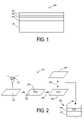
- FIG. 1provides a schematic illustration of an enhanced layered display system according to an embodiment of the present disclosure.
- FIG. 2illustrates a process for providing an optical layer for a display system according to an embodiment of the present disclosure.
- FIG. 3illustrates a method of laminating an adhesive preform unit to create an enhanced layered display system.
- FIG. 4illustrates another method of laminating an adhesive preform unit to create an enhanced layered display system.
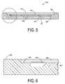
- FIG. 5illustrates an adhesive pool to create an adhesive preform unit.
- FIG. 6illustrates an enlarged sectional view of an adhesive pool to create an adhesive preform unit.
- FIG. 7shows a perspective view of an adhesive pool to create an adhesive preform unit.
- FIG. 8illustrates an enlarged sectional view of another adhesive pool to create an adhesive preform unit.
- FIG. 9illustrates a method for injecting the optical bonding liquid into the adhesive pool.
- FIG. 10illustrates a method for leveling the optical bonding liquid in the adhesive pool.
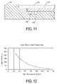
- FIG. 11illustrates an enlarged sectional view of an example system for removing the adhesive preform unit from the adhesive pool.
- FIG. 12shows a graphical representation of a variation of cure time as a function of cure temperature for the adhesive preform unit.
- FIG. 13illustrates a release liner for the adhesive preform unit.
- FIG. 14illustrates a method utilizing a sheet of mother glass as the substrate and singulating the sheet to for individual adhesive preform units.
- FIG. 15illustrates a method of coupling an adhesive preform unit to a display.
- FIG. 16illustrates an example alignment fixture for coupling an adhesive preform unit to a display.
- FIG. 17shows a cut-away view of an example system for providing a vacuum environment for coupling an adhesive preform unit to a display.
- FIG. 18shows a sectional view of the example system of FIG. 17 for providing a vacuum environment for coupling an adhesive preform unit to a display where the adhesive preform unit and display are aligned but not yet in contact.
- FIG. 19shows a sectional view of the example system of FIG. 17 for providing a vacuum environment for coupling an adhesive preform unit to a display where the adhesive preform unit and display are in contact.
- FIG. 20shows an example vacuum laminator for coupling an adhesive preform unit to a display.
- FIG. 21shows the example vacuum laminator of FIG. 20 for coupling an adhesive preform unit to a display where the piston has been extended for making the bond between the adhesive preform unit and a display.
- FIG. 22illustrates another process for providing an optical layer for a display system according to an embodiment of the present disclosure
- FIG. 23provides a further example of a process for providing an optical layer for a display system according to an embodiment of the present disclosure.
- FIG. 24shows a process flow depicting a method of generating an enhanced layered display system.
- FIG. 1provides a schematic illustration of an embodiment of an enhanced layered display system 100 according to an embodiment of the present disclosure.
- an enhanced layered displaymay be any suitable display, such as LCD 102 , in combination with at least one overlay, such as overlay 106 .
- overlay 106may be any suitable display, such as LCD 102 , in combination with at least one overlay, such as overlay 106 .
- enhanced layered display system 100may be a flat panel display, a cellular phone display, a monitor, a television display, a display for a personal data assistant or other portable computing device, outdoors displays, industrial displays, medical displays, navigational displays, or other electronic presentation, data, or graphic display.
- enhanced layered display system 100may be an interactive display, such as a touch display, a light pen display, a graphics tablet, etc.
- display system 100may also be a substrate.
- display system 100may be a touch switch, glass, a filter, a vandal shield, etc.
- display system 100may include LCD 102 where each pixel of the LCD generally includes a layer of liquid crystal disposed between two transparent electrodes, and two polarizing filters, the axes of polarity of which are perpendicular to each other. Selectively applying a voltage to the electrodes (and the resultant configuration change of the liquid crystals) enables control of whether light is either transmitted or absorbed such that images may be formed on the display. Additional information regarding LCDs may be found in U.S. Pat. No. 6,933,991 entitled Super Bright Low Reflectance liquid Crystal Display issued Aug. 23, 2005 and U.S. Pat. No. 6,181,394 entitled Super Bright Low Reflectance Liquid Crystal Display issued Jan. 30, 2001, both of which are hereby incorporated by reference for all purposes.
- the LCDs shown in the exemplary figuresare illustrated schematically and the specific liquid crystal layers, polarizers, etc. are not shown in detail.
- the present disclosureis directed to the outside interface of the LCD such that an overlay 106 in the form of an optical layer (and/or protective layer) may be coupled to the external surface of the LCD.
- the disclosureis directed to the bonding of the overlay to the LCD, it should be understood that the disclosed layering techniques herein, can be applied to other layers of an LCD or even to other optical devices having two or more layers.
- the LCD 102includes a first or external facing substrate 104 , such as a glass substrate, which is disposed on the exterior surface or face of the LCD 102 .
- first substrate 104may be the polarizer of the LCD.
- a second substrate or overlay 106may be applied to the first substrate 104 to provide enhanced layered display system 100 .
- the inside surface of overlay 106is positioned to face the exterior surface of LCD 102 , such as substrate 104 .
- the second substrate 106may be any suitable material and may have an index of refraction similar to the index of refraction of the first substrate, although this matching is not required in all embodiments. It should be appreciated that the substrates may be any suitable materials, and need not be the same material, including but not limited to glass, plastic, etc.
- first substrate 104 and second substrate 106Disposed between first substrate 104 and second substrate 106 may be an optical bonding layer 108 composed of a bonding material.
- This bonding materialmay be a solid, gel or liquid.
- optical bonding layer 108is an index-matched material such that the indices of refraction are substantially similar to one of the first substrate 104 , the second substrate 106 or both.
- the first substratemay be glass and have an index of refraction of 1.472 such that the bonding layer has an index of refraction of 1.406.
- the bonding material of optical bonding layer 108may be an optical adhesive. Although primarily described as an optical adhesive, in some embodiments, it should be appreciated that the bonding material may have little or no adhesion qualities and may be primarily an optically matched layer. In such non-adhesion embodiments, the layers may be held together via alternative means.
- the bonding materialmay be a combination adhesive which is considered in application as a pre-cured optical adhesive.
- the bonding materialmay be applied as a liquid adhesive, also referred to herein as an optical bonding liquid, to one or both of the first substrate 102 and second substrate 106 .
- the bonding liquidmay be fully or substantially cured to form an adhesive preform, and following curing, the second substrate may be laminated onto the display.
- the bonded enhanced layered display system 100may be post-processed to increase the adhesion strength of the bond and drive any entrapped air from the optical bond.
- the bonding materialmay be a silicon-based bonding material.
- the bonding materialmay be other suitable materials, including, but not limited to, urethane derivative materials and/or acrylic derivative materials.
- the bonding materialmay be a mixture of a urethane derivative and a silicone derivative (and/or acrylic derivative). The mixture of the harder urethane-derivative with the softer silicone-derivative may provide additional bonding characteristics.
- bonding to glassmay be with a urethane-derivative, and/or bonding to the display may be with a silicone-derivative. Further, in some embodiments, it may be possible to use an epoxy derivative.
- the following specific materialsare provided as illustrative example materials and may be used alone or in combination.
- Options for bonding materialsinclude gels, elastomers and resins, including but not limited to, a mixture of dimethyl-siloxane and vinyl terminated dimethyl polymer with a hydrosilane crosslinking agent, a mixture of dimethyvinylsilioxy-terminated phenylmethyl cyclosiloxanes, methylvinyl siloxane, dimethoxy (glycidoxypropyl)-terminated, and/or polyether based aliphatic polyurethane.
- a multi-layer approachmay include use of acrylic optically clear materials. Further a thinner may be applied to decrease the viscosity to the bonding material and assist in lamination. A material with a drying rate similar to acetone may be used such as hexamethyldisiloxane to achieve these effects.
- FIG. 2provides a schematic illustration of a laminating pre-cured optical adhesive process 200 for providing the display system of FIG. 1 .
- an adhesivemay be applied and cured to a single substrate prior to coupling the first and second substrate together.
- substrate 202is illustrated in FIG. 2 as the overlay, although it should be appreciated that in some embodiments, the display, such as an LCD display, may be considered as the first substrate.
- Bonding material 204may be applied to the surface of substrate 202 .
- bonding material 204may be an optical bonding liquid.
- the bonding materialmay be a pressure sensitive adhesive in a liquid carrier.
- the bonding materialmay be poured and leveled on the first substrate. This initial step may be considered the self-leveling step.
- the bonding material 204may be prepared on a separate surface or liner and then removed for application to the first and second substrate. Formation of the bonding layer using a liner may create a bonding sheet which may be used as described in more detail below.
- bonding material 204may be cured as indicated at 205 .
- the bonding material 204may be cut to size, if necessary.
- a double cure systemmay be used where the bonding material is cured at ambient temperature and then with heat or autoclaved. The resulting bonding material forms the bonding layer.
- the bonding layeris of a minimum thickness of 0.004 inches (10 mm). The depth of the bonding layer may be based, in part, on generating a uniform surface which accommodates variances in the substrate surfaces.
- the bonding materialmay be selected based on a plurality of factors, including but not limited to: optical qualities, such as the index of refraction of the material, and mechanical qualities, including bonding characteristics and curing speed. Materials that cure too quickly may be difficult to set in the layered complex. Further, materials that cure too slowly may result in increased production time and costs.
- substrate 202may be considered to have a prepared surface 206 with cured bonding material, also referred to as the adhesive preform 206 .
- a second substrate 208may be applied as indicated by arrow 210 to the prepared surface 206 of substrate 202 to create a layered display system 212 .
- the bonding materialmay be cured (either at ambient temperature or through heat/pressure) prior to coupling of the first and second substrate and the entire complex may be autoclaved again following the coupling of the first and second substrate to the bonding material.
- the above process of preforming the bonding layermay reduce defects in the bonding layer. Further, the formed layer is substantially more uniform than conventional layers and may be uniform within 0.001 inch thickness.
- the laminating pre-cured optical adhesive process shown in FIG. 2allows the speed and simplicity of the PSA lamination process to form the optical bond between the display and overlay, while offering the desirable properties of the form-in-place liquid adhesives. Further, this pre-form lamination process enables the bonding layer to be much thicker than available with PSA sheets. This increased thickness allows the incorporation of optical bonding in customized and specialty displays, such as displays with perimeter bezels, which protrude from the front surface of the display. Additionally, the added thickness may be advantageous in interactive systems. For example, the additional thickness which can be created using the laminating pre-cured optical adhesive process, described above, may reduce stress placed on the display from touch pressure placed on the overlay in a touch or stylet display system.
- defects in the curing processmay be identified prior to applying the second substrate.
- the substratesmay be coupled to additional layers (such as to the LCD panel), it is possible to control which substrate would be discarded upon detection of a defect. Since typically the overlay is less expensive than the LCD, defect identification prior to coupling of the LCD may result in preventing destruction or loss of LCDs during manufacture.
- the laminating pre-cured optical adhesive method and resulting apparatusmay have enhanced viewing characteristics, such as brightness, through the addition of the optical layer coupling. Further, the optical layer coupling may result in improved ruggedness with reduction in defective product production.
- FIG. 3provides another illustration of a method 300 of laminating the adhesive preform to create an enhanced layered display system.
- Optical bonding liquid or materialmay be applied to the substrate 302 directly.
- the bonding materialmay be any suitable bonding material as described above.
- the bonding materialmay be a two-part platinum cured silicone adhesive with added adhesion promoters.
- the bonding materialas used in these examples, is tacky in the fully cured state.
- the desired bond-line thicknessmay be generated as the bonding material is applied to the substrate.
- the bonding materialmay be cured using a suitable curing system, including, but not limited to self-curing, light curing, such as UV or IR curing, heat curing, pressure curing, chemical curing, etc.
- the type of curingmay be based on the formulation of the bonding material.
- self-curing adhesivesmay increase their cure rate by raising the temperature, which can be used to increase throughput.
- the adhesive layercan be fully exposed directly to a light source. The ability to directly expose the adhesive layer facilitates improved curing in contrast to prior systems where shadowing may affect the curing process.
- the overlayprevents the light source from directly penetrating the adhesive (the overlay is between the adhesive and the light source) and the overlay may negatively affect the light-initiated cure.
- the bonding materialcan be placed directly onto the overlay individually.
- the bonding materialmay completely or substantially cover the overlay, such as when the display has no bezel and the overlay is the same or smaller size than the display glass, or when the overlay would fit entirely within the bezel of the display.
- the bonding materialmay not cover the entire overlay, instead the bonding material may be specially shaped to match to the display.
- a shaped preformmay be used when the overlay extends over the bezel of the display, or even overhangs the display.
- substrate 302may be considered to have a prepared surface with cured bonding material, also referred to as the adhesive preform.
- FIG. 3illustrates an edge-to-edge preform 304 on substrate 302 .
- FIG. 4illustrates a shaped perform 404 on substrate 402 .
- the edge-to-edge perform 304corresponds to the top polarizer 306 of LCD 312 .
- the overlay substrate and the top polarizerare substantially the same size.
- the LCD layers 308 and bottom polarizer 310complete the enhanced layered display system.
- the shaped preform 404is selectively sized on the overlay 402 .
- the size of shaped preform 404may correspond to features on the display 406 , such as the size of an opening in the bezel of the display.
- the shaped perform 404is substantially sized to correspond to the bezel opening 412 in bezel 410 .
- the shaped preform in FIG. 4is substantially the same size as top polarizer 408 . It should be appreciated that not all systems will include a top polarizer and/or the top polarizer may be a different size than the shaped preform.
- a substantially uniform thickness bond-lineis desired.
- the overlaymay be positioned in an adhesive pool, where the adhesive is then applied to the overlay to generate a substantially uniform thickness bondline.
- the thickness of the bond linecan be such to accommodate any suitable display.
- the bond line depthmay be such to accommodate displays larger than 5.0′′ diagonal, where the minimum thickness of the optical adhesive between the top polarizer and the overlay is typically 0.5 mm to as much as 3.0 mm.
- FIG. 5illustrates an embodiment showing use of an adhesive pool to generate a substantially uniform thickness bond-line.
- an adhesive pool 500may be provided with a frame 502 and at least two depth levels, level one indicated at 504 and level 2 indicated at 506 .
- additional levelsmay be provided to accommodate different sized overlays and the two level system is shown for the purpose of example.
- the poolmay be configured to define an opening or cavity to receive the overlay 508 .
- the overlaymay be supported on overlay supports 510 , such as the floor of level 2, in the adhesive pool. After positioning the overlay on the overlay supports 510 the pool may be filled with the bonding material 512 .
- the adhesive poolmust be substantially free of leaks which would result in depressions in the bond-line.
- the overlay supports 510ensure that the overlay 508 is in a level non-sloped orientation in order to prevent variation in the bonding material on the overlay when the bonding material is inserted into the adhesive pool.
- the floor of the poolis depressed to create level 2, indicated at 506 , such that the depression in the floor corresponds to the shape of the overlay.
- the overlaymay be inset into the depression, where the overlay supports 510 maintain the overlay 508 in substantially planar orientation.
- overlay 508is supported such that level 1 of the pool, indicated at 504 , is substantially co-planar with the top surface 514 of overlay 508 .
- the coplanar leveling of the overlay with the bottom of the poolmay operate to prevent a change in adhesive thickness at the edge of the overlay.
- a non-planar overlaymay be used.
- the overlaymay be non-planar, it may be possible to use the above-described methods to generate the desired adhesive preform on such an overlay.
- the overlaymay be spherical-shaped or another specialty shaped overlay.
- the overlaysthemselves may be custom-shaped for a desired application.
- the overlaysmay be non-rectangular overlays, where the overlay may be trapezoidal, circular, oval, star-shaped, or other custom shape.
- the adhesive preformmay be similarly-shaped to the overlay depending on the application.
- the adhesive preformmay be shaped to correspond to the shape of the display. The shaping of the overlay and the display are customized features which can be incorporated into a select layered system.
- the adhesive poolmay further include features to reduce non-uniformity of the bonding material to the edges of the overlay.
- the overlayis positioned within level 2, where there is sufficient area extending beyond the edges of the overlay as indicated by level 1 at 504 . If the edges of the pool are engaged against the edge of the overlay, there are edge effects on the adhesive where it meets to edge of the pool. For example, the surface tension of a liquid adhesive may result in formation of a meniscus at the edge interface. By controlling the meniscus, a flat, uniform bond-line may be along the overlay. By providing an extended-edge area, any such edge effects are substantially removed from the edge of the overlay by forming a larger area adhesive pre-form beyond the perimeter of the overlay.
- the “edge effect zone”is pushed outwards away from where the bond will be completed against the overlay.
- 2 mm spacingis provided between the outer edge of the overlay and the outer edge of the pool frame.
- the overlaymay be removed from the pool and the excess perform is carefully cleaned from the edges of the overlay and also cleaned from the pool. It should be appreciated that other methods, including use of materials, adhesive pool shape design and environmental conditions may be used to control the meniscus and other edge effects.
- adhesive poolsmay be used, including pools which create a substantially-identically sized preform.
- the tiered designmay be eliminated, such that the overlay may be positioned at the bottom of a straight walled pool.
- Such poolsreduce the use of bonding material as little or no bonding material is wasted on the sides beyond the overlay.
- the reduction in bonding materialmay reduce the costs associated with the bonding material. Further, cleaning steps may be reduced with such pools.
- a masking layermay be included prior to insertion of the bonding material in the pool.
- an overlay 602may be positioned in an adhesive pool 600 .
- the top layer of the overlay 602may be substantially coplanar with level 1 edge 604 .
- Overlay 602may be masked as indicated at 606 such that when bonding material 608 is deposited into pool 600 , the bonding material adheres to the masked portion of the overlay and is removed with the mask as it is pulled away.
- the overlaymay be preprinted or preprocessed prior to application of the adhesive to create specialty or custom overlays.
- preprinting or preprocessingmay be used for masking, for aesthetic applications, for functional purposes, such as touch screens, etc.
- Such preprinting and preprocessingmay be understood to be features of the overlay.
- portions of the overlaymay be darkened, tinted, colored, or pre-printed with various graphics, wording, shadings, etc.
- the methods and systems hereinenable such features to be accommodated without significant increase in processing.
- a preprocessed sheetmay have holes or other features included in the glass overlay. The holes may be for mounting, speakers, touch sensors, etc. Additional printing may be included on the overlay to enable various functionalities or maintain a desired aesthetic of the display. For example, design printing or logos may be provided on the overlay.
- FIG. 7shows a perspective view of an adhesive pool 700 with an overlay 702 positioned within the depression formed by level 2, as indicated at 704 .
- the floor of level 1, indicated at 706is substantially coplanar with the top surface of overlay 702 .
- Masking 708extends around the perimeter of overlay 702 to form a specialty-shaped preform. Such masking may enable a shaped preform to be generated for use in aesthetically varied designs. Although shown in the shape of a uniform rectangle, other shapes and variations on such shapes are considered and within the scope of this disclosure.
- FIG. 8further illustrates another method of creating a shaped preform. Similar to FIGS. 6 and 7 , an overlay 802 may be positioned in an adhesive pool 800 . Masking 804 may extend over the overlay and over the bottom edge of level 1, at 806 . Bonding liquid 808 may be dispensed on top of the overlay to form an adhesive preform unit. The additional masking may provide easier release of the overlay and preform from the adhesive pool such that there is minimized disruption to the shaped preform upon release.
- FIG. 9shows a dispenser 900 for injecting bonding material into an adhesive pool 902 .
- the dispenser 900may include a paddle-tipped head 904 to ensure an even injection of bonding material across the overlay 906 .
- the paddle-tipped head 904may release the bonding material at a controlled rate as it is moved across the overlay as indicated by arrow 908 .
- the bonding materialmay be selectively released such that it is deposited into the adhesive pool where it is substantially level with the top surface of the pool.
- the poolmay be sized such that the pool depth corresponds to the depth of the desired bond-line thickness.
- the bonding materialmay be injected into the pool evenly with exactly the proper amount of bonding material to completely fill, but not overfill the pool.
- the low viscosity of the bonding materialwill allow it to self level and flow a short distance to fill out the form. Filling the pool results in creation of a preform with the desired bond-line thickness.
- dispenserscan be used to dispense an even line of bonding material across a series of adhesive pools.
- the surface of the bonding materialmay be further leveled using an edger or squeegee 1000 as illustrated in FIG. 10 .
- excess adhesive 1002 that has been injected into poolmay be removed by drawing the edger across the top surface, evenly filling the pool 1004 and moving the excess material out beyond the edge.
- the dispenser and edgermay be a single unit, such that use of the combination dispenser and edger results in injection of bonding material to form a level bond-line thickness over the overlay.
- the bonding materialAfter injection and leveling of the bonding material, the bonding material is cured. Any suitable method for curing the bonding material may be used. It is noted that the bonding material may be fully cured in the adhesive pool or it may be removed with the overlay from the adhesive pool and then fully cured.
- the formulationsare self curing.
- the adhesivesmay be cured at room temperature in 4 hours and can be accelerated to 2 hours at 50° C.
- a substratesuch as a glass overlay
- much higher temperaturescan be used without damaging the substrate.
- the adhesivefully cures in 10 minutes, and as little as 3 minutes at 200° C.
- FIG. 12shows a graphical representation of a variation of cure time as a function of cure temperature.
- the use of the overlay as the substrateenables the use of high cure temperatures. For example, temperatures of over 100° C. may reduce the cure time to less than one hour.
- the substrate, where the substrate is the overlay, such as a glass overlayis not affected by the use of such high temperatures. In contrast, use of such high temperatures on the LCD would negatively effect operation of the LCD and would result in possible failure of the completed system.
- the curingmay be accelerated using IR heaters or other suitable heating system.
- IR heatersor other suitable heating system.
- silicone adhesivessince the silicone is transparent to IR wavelengths, the IR energy is transmitted through the silicone and is adsorbed by the substrate.
- the adhesiveis heated uniformly from below (from the heated substrate) and is quickly cured in a very controlled manner.
- a contact heating approachis utilized where the substrate (the overlay) is in contact with a hot plate where the temperature can be accurately controlled. A full cure in less than 3 minutes is possible when a silicone adhesive is applied to a 200° C. substrate.
- a conventional convection ovencan be used using hot air to heat the adhesive.
- Another embodimentprovides a two-stage system, where the bonding material is applied to the substrate and then a pre-heated nickel Teflon coated aluminum plug is applied from the top of the bonding material.
- the distance from the top of the bonding material to the top of the overlaycan be controlled, enabling control over the bond line thickness and the quality of the top surface of the adhesive pre-form through shaping of the plug.
- FIG. 11An example system for removing the overlay with the adhesive preform from the adhesive pool is illustrated in FIG. 11 .
- overlay 1102is positioned in adhesive pool 1100 .
- Bonding material 1104has been injected into adhesive pool 1100 such that the overlay 1102 and bonding material 1104 form an adhesive preform unit, also referred to as an adhesive preform overlay unit.
- vacuum channels 1106 and seals 1108may be used to retain the adhesive preform unit in the adhesive pool and minimize leakage during with use of a vacuum.
- Release of the adhesive preform unitmay be assisted by use of easy-release materials. Clean, non-contaminated materials for the adhesive pool may prevent unwanted sticking of the bonding material to the adhesive pool. Further, coating of the adhesive pool may increase and ease debonding. For example, the adhesive pool may be coated in nickel-PTFE.
- a release linermay be applied to the surface of the bonding material.
- FIG. 13illustrates a release liner 1300 protecting the external surface of the adhesive preform 1302 where the adhesive preform is coupled to the overlay substrate 1304 .
- the release linermay enable contact with the surface of the bonding material without contamination of the fragile optical surface. Contact with an uncovered top surface of the bonding material may result in contamination and marring of the surface.
- the over-sized preformcan be used to release the adhesive preform unit from the adhesive pool. Although the extended edge of the over-sized preform is thin and fragile, the combination of easy-release materials and the use of the liner may assist in release of the adhesive preform unit from the adhesive pool.
- the release linermay also advantageously protect the pre-form from contamination and damage.
- release linersmay be materials such as low density polyethylene (LDPE). To be effective, the liner must be substantially free from contaminants and particulates.
- LDPElow density polyethylene
- vacuum channels 1106can be used to grip and subsequently release the adhesive preform unit. As shown, these vacuum channels may be built into the adhesive pool.
- multiple adhesive poolsmay be aligned such that a plurality of overlays may be processed together.
- a fluid dispensermay be used having multiple heads or other arrangement where the fluid dispenser may releases adhesive into multiple adhesive pools simultaneously or successively.
- the adhesive preform unitsmay be selectively cut to generate individual units.
- the use of a grouped setincreases manufacturing efficiency as it may be possible to generate a significant number of individual units using a single substrate platform.
- a release linermay be applied to the exposed adhesive on the adhesive preform unit to protect the adhesive and prevent contamination until the adhesive preform unit is laminated to a display
- FIG. 14shows an embodiment where a sheet of mother glass 1400 is treated as the substrate.
- An adhesive 1402may be applied to the sheet 1400 to form an adhesive preform unit which can be singulated for individual displays 1404 .
- the sheet 1400may be scribed before application of the adhesive to allow any debris generated by the scribing process to be cleaned prior to coating. Once coated and cured, sheet 1400 can be broken along the previously scribed lines and singulated.
- sheet 1400may be scribed and broken after the adhesive has been applied and cured. For example, the sheet may be scribed using laser scribing or other process that minimizes generation of debris.
- the singulated unitsmay have raw edges that are seamed to remove sharp features. Further, such edge seaming may improve mechanical performance by reducing crack initiators.
- the sheetsmay be preprinted or preprocessed prior to application of the adhesive to create specialty overlays.
- preprintingmay be used for masking, for aesthetic applications.
- a preprocessed sheetmay have holes or other features included in the glass.
- sensorssuch as touch sensors may be incorporated onto the overlay sheet. After the adhesive is applied to the sheet and cured, the sheet may be singulated to yield individual overlays with the specialty features in the desired position.
- a release linersuch as low density polyethylene (LDPE) may also be added to the coated mother glass to allow for storage and shipment prior to singulation.
- LDPElow density polyethylene
- the adhesive pre-formscan also have the release liner added after the mother glass is singulated.
- an adhesive preform unitan overlay with a cured adhesive preform
- such adhesive preform unitis configured to be laminated to a display to form an enhanced layered display system.
- individual adhesive preform unitsmay be laminated to the corresponding display as described in more detail below. If a release liner is present, it is first removed and then the adhesive on the overlay is then brought in contact with the clean, top polarizer on the display. Pressure may be added over time to the bond to assure a good tack.
- FIG. 15illustrates at 1500 coupling of an adhesive preform unit 1502 to a display 1508 .
- Adhesive preform unit 1502includes an overlay substrate 1504 and an adhesive preform 1506 .
- the adhesive preformis a shaped pre-form where the overlay with an in-bezel bond. It should be appreciated that any the preform may be configured, such as a shaped or edge-to-edge preform, depending on the dimensions and desired aesthetic appearance of the resulting layered display system.
- a dedicated alignment fixturemay be used to properly position the overlay with respect to the display to assure proper positional alignment within tight tolerances.
- fixturing systemshave shown to be accurate to within +/ ⁇ 0.02 mm in volume production.
- a robotic or semi-robotic systemmay be used to perform the lamination.
- dedicated fixturingmay not be necessary for each specific part geometry as the robotic system may incorporate an active alignment or positional system to accurately determine the position and orientation of the overlay and the display and compensate to properly align the assembly.
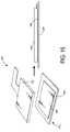
- FIG. 16illustrates an example alignment fixture 1600 .
- Alignment fixture 1602includes a display receiver 1602 for display 1604 .
- the adhesive preform unit 1606may be positioned in channel 1608 such that the overlay and display are properly aligned. It should be appreciated that the alignment fixture may have receivers of various shapes to correspond to the dimensions of the display and the overlay.
- the adhesive in the adhesive preform unithas already fully cured, the bond between the overlay and the display is made and the parts held together instantly upon contact. In contrast to prior systems, there is no need to wait while the adhesive cross links.
- the immediate bondingreduces the number of alignment fixtures or robotic alignment and lamination stations needed, decreasing equipment investment and, resulting in increased production efficiency.
- the adhesive preform unitis deformed slightly prior to laminating.
- the adhesive preform unitcan be deformed into a section of a cylinder. In this way, lamination begins as a line contact, and then the adhesive preform unit is rolled onto the display, keeping a continuous advance of the bonded area and substantially eliminating any trapped air pockets.
- the adhesive preform unitcan be deformed into a section of a sphere by fixing the corners and pushing the center towards the display. Lamination is initiated at a point in the center of the display and the bonded area then spreads from there as the amount of deflection in the adhesive preform unit is decreased. Again, with such embodiments, the air bubbles are minimized during the lamination process improving the quality of the laminated system.
- the lamination processis completed in a vacuum environment.
- the vacuum environmentmay substantially reduce or eliminate air bubbles that get trapped during the lamination process.
- the adhesive preform unit and displayare placed within the vacuum chamber, which is evacuated. Once the pressure in the chamber reaches the desired level, the adhesive preform unit may be brought in contact with the top polarizer on the display.
- the enhanced layered display systemis post-processed to eliminate any air entrapped during the lamination process.
- the coupling of the adhesive preform unit to the displaymay result in the capture of small amounts of air between the overlay and the display, e.g. the LCD glass.
- the air bubblescreate optically visible flaws which affect the quality of the system.
- the enhanced layered display systemis placed under pressure and elevated temperature.
- the enhanced layered display systemsmay be heat and pressure processed.
- some systemsmay be post-processed at 0.5 MPa (72.5 psi) and 50° C. for 20 minutes.
- the enhanced layered display systemsare post processed under pressure only, e.g. with 0.41 MPa (60 psi) pressure for as little 10 minutes.
- the optimal processing schedulemay vary depending on different display size and bond thickness combinations.
- the systemsmay be post processed using a combination of heat and pressure for periods varying from ten to sixty minutes depending on the intensity of the heat and pressure.
- the post-processing procedureuse a heated autoclave which uses pressures in excess of 0.5 Mpa and temperatures approximately 45° C. for up to forty five minutes to drive the bubbles out from between the display and the overlay and produce a fully-cured, optically clear bond.
- the bondsmay be examined or tested for flaws, optical quality or other performance issues.
- the adhesive and cohesive strength of the optical bonddoes not change significantly during post processing, but any air bubbles can be substantially eliminated. It further should be appreciated that the post-processing may be eliminated or reduced for systems which have little or no bubble formation during lamination, such as the vacuum lamination process described in more detail below.
- the adhesive preform unitmay be laminated to the display in a vacuum environment. Laminating the adhesive preform unit and the display in a vacuum may eliminate any residual bubbles, and negate the requirement for post processing the laminated assembly with heat and pressure, allowing the finished product to be inspected and packaged immediately after the lamination process.
- the lamination processmay be a 30 second process and packaging may occur immediately after the lamination process.
- Such a systemmay result in a total work in process inventory time reduction of over forty-five minutes (where the post processing system requires both heat and pressure processing), to less than one minute with the vacuum lamination. Further, and the elimination of post processing provides a more direct lean production system. Such advantages lead to the ability to produce a high volume of display systems and reduce costs on production of such systems.
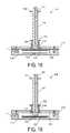
- the adhesive preform unit 1702is loaded onto a holder 1704 in the upper housing 1705 of vacuum laminator 1700 .
- Holder 1704is mounted on a piston 1706 positioned in a sealed cylinder 1708 .
- Cylinder 1708may be permanently mounted in the upper housing of the vacuum chamber.
- Locating pinssuch as pin 1714 , may be used to align the upper and lower houses of the chamber.
- One or more perimeter compliant members, such as rings 1716may form a seal, and a vacuum is pulled through a hole in the chamber.
- the spring 1718 on the pistonprevents the vacuum from pulling the piston down. Washers 1720 are further illustrated in FIG. 17 .
- a vacuum pumpsuch as piston 1706
- piston 1706may be engaged, such as by pressing the piston down by either hand or machine force.
- the adhesive preform unit 1702 and display 1712may be coupled.
- the vacuumis released, standard pressure achieved and the chamber opened to remove the enhanced layered display system, now laminated and substantially bubble free.
- no post processingis needed to complete the bond.
- FIG. 17illustrates the vacuum laminator 1700 in a position ready for bonding.
- adhesive preform unit 1702 and display 1714are positioned in the upper and lower housing respectively such that upon contact the overlay and display are in the desired alignment.
- FIG. 18shows a sectional view of the vacuum laminator 1700 with the piston in position prior to bonding adhesive preform unit 1702 and display 1714 .
- FIG. 19shows another sectional view of the vacuum laminator 1700 , where the piston 1706 has been moved to bond adhesive preform unit 1702 and display 1712 together.
- FIGS. 20 and 21illustrate another embodiment of a vacuum laminator.
- the vacuum laminator 2000is shown in an open position ready for loading of an adhesive preform unit into the upper housing 2002 and loading of a display into the lower housing 2004 .
- FIG. 20shows piston 2006 retracted for loading and for pulling a vacuum.
- FIG. 21shows piston 2006 extended for making the bond between the adhesive preform unit and display. It is noted that a seal 2008 on lower housing 2004 is provided to prevent leaks in the housing.
- a gauge 2010for measuring the vacuum in the chamber and a shut-off valve 2012 for shutting off the chamber from the vacuum source.
- FIG. 22provides another embodiment of a layered display.
- Layered display 2200may include a first substrate 2202 and a second substrate 2204 .
- An optical bonding layer 2206may be disposed between first substrate 2202 and second substrate 2204 .
- Optical bonding layer 2206may be an adhesive, such as a pressure sensitive adhesive sheet or a fully cured transfer adhesive, such as the adhesive described above.
- the adhesive sheetmay have an index of refraction designed to minimize reflections from the first and second substrates.
- the bonding layermay be of substantial thickness to accommodate, in part, extended topographies and allow a defect free layer in the first and second substrate.
- the bonding layersuch as the bonding layers described above, may be approximately 0.010 inch (0.25 mm) thick.
- an optical adhesivesuch as a two-part platinum cured silicone adhesive
- a release linersuch as an LDPE release liner.
- the adhesivemay then be cured and a second release liner positioned on the previously exposed surface.
- This transfer adhesivecan then be stored and shipped as a sheet.
- one release linermay be removed and the transfer adhesive may be laminated to the overlay or display.
- the second release linermay be removed and the display or overlay is then laminated in place.
- the bondcan be post-processed to remove any trapped air.
- the transfer adhesive sheetmay enable the adhesive processing to be separated physically and geographically from the laminating process. Moreover, the transfer adhesive sheet may be selectively cut to the desired size easily for late stage differentiation in the production cycle allowing significant variation in products. Finally, the adhesive can be made in large sheets (or even roll to roll).
- the transfer adhesivemay be made in fixed size tools or forms.
- roll-to-roll methodswhere the adhesive is extruded onto a roll of release liner and cured, and then the second liner is rolled onto the previously exposed surface may be used.
- FIG. 23provides another embodiment of a layered display according to an embodiment of the present disclosure.
- Layered display 2300includes a first substrate 2302 and a second substrate 2304 . Disposed between first substrate 2302 and second substrate 2304 is a bonding layer 2306 .
- Bonding layer 2306may include a plurality of adhesive sheets 2308 , 2310 , 2312 , such as pressure sensitive adhesive sheets or transfer adhesive sheets. The sheets may be stacked to form an optical enhancement layer. Each sheet may have a suitable index of refraction that it that is designed to reduce the reflections from the first and second substrates.
- the sheetsmay be made of the same material or of different material.
- some sheetsmay be a urethane-derivative, while others may be a silicone derivative or acrylic-derivative.
- the sheetsmay be of the same or different thickness.
- bonding layer 2306may be of substantial thickness to accommodate extended topographies in the first and second substrate.
- the bonding layermay be approximately 0.010 inch (0.25 mm) thick.
- each sheetmay be of such thickness that the total bonding layer is approximately 0.010 inch (0.25 mm).
- bonding layers 2308 , 2310 , or 2312may be comprised of one or more non-adhesive optical enhancement layers. These layers may be pressed or trapped between the two substrates and may be used alone or in combination with an adhesive.
- the bonding materialmay be a non-adhesive optical enhancement layer which may be sandwiched between the first and second substrate and retained through clamps or frames. The index of refraction of the layers are designed to provide optical enhancement for the display, but provide little or no adhesion qualities.
- the displaymay further include a bezel.
- multiple applicationsmay be necessary to provide sufficient bonding layers. For example, two applications may be used, one on the display and one on the bezel. Combination bonding materials may be used with such systems.
- FIG. 24shows a process flow depicting an embodiment of a method of generating an enhanced layered display system.
- Method 2400comprises, at 2402 , dispensing an optical bonding liquid onto a first substrate; accelerating curing, at 2404 , of the optical bonding liquid to form an adhesive preform unit; and laminating, at 206 , the adhesive preform unit to a top surface of a liquid crystal display to form the enhanced layered display system.
- the dispensing of an optical bonding liquid onto a first substrate and the curing to form an adhesive preform unitmay be performed in a first location and the laminating step performed in a second location.
- the adhesive preform unitmay be transported for lamination and processing in a different facility at a subsequent period of time. If the adhesive preform unit is generated for later use, a release liner may be used to prevent contamination of the adhesive preform.
Landscapes
- Physics & Mathematics (AREA)
- Nonlinear Science (AREA)
- Optics & Photonics (AREA)
- Mathematical Physics (AREA)
- Chemical & Material Sciences (AREA)
- Crystallography & Structural Chemistry (AREA)
- General Physics & Mathematics (AREA)
- Liquid Crystal (AREA)
- Devices For Indicating Variable Information By Combining Individual Elements (AREA)
Abstract
Description
- The present application claims priority to U.S. Provisional Patent Application Ser. No. 60/918,974 of Maria Crouser and Scott Engle, entitled ENHANCED LIQUID CRYSTAL DISPLAY DEVICE filed Mar. 19, 2007, the disclosure of which is hereby incorporated by reference.
- The present application relates to systems, apparatus and methods for interfacing optical layers, and more particularly systems, apparatus and methods for enhancing a liquid crystal display device.
- Display devices, such as liquid crystal displays (LCDs) or organic light emitting displays (OLEDs), are used in a variety of environments. Depending on the use environment and application of the display device, brightness and contrast features of the display device may be of significant value. For example, use of a display device in an outdoor environment or in an environment with high ambient light may require increased levels of contrast and/or brightness to maintain a desired level of viewability.
- Typical LCDs comprise a liquid crystal display panel having a thin film of liquid crystals sandwiched between a pair of transparent electrodes. The liquid crystal display panel typically includes a pair of glass plates, the glass plates being sealed together around their respective edges. The glass plates may be assembled with spacers between them to maintain a constant separation distance. Two crossed axis polarizers may be adhered to the respective inside surfaces of the glass plates, one polarizer being adhered to the front of the liquid crystal display panel and the other polarizer being adhered to the rear of the liquid crystal display panel. When a voltage is applied selectively across the electrodes, the liquid crystal molecules between them may be rearranged or switched in polarization so that light is either transmitted or absorbed in the output polarizer to form characters or graphics.
- LCDs may include a layer of indium tin oxide or another suitable material positioned between, or in front of, the front polarizer and the front glass plate for use as an electromagnetic interference shield. Some LCDs, intended for use in cold environments, also include a layer of indium tin oxide or another suitable material positioned between the rear polarizer and the rear glass plate and electrically connected to a power source for use as a heating element.
- LCDs may be susceptible to back-reflected ambient light such that the viewing characteristics of the display deteriorate under high ambient light conditions, such as when placed in direct sunlight. Various methods have been used to improve the viewing characteristics of the LCDs. For example, in some embodiments, anti-reflection coatings have been applied to the front of the display. As another example, additional optical layering has been used to improve the viewing characteristics and to improve the durability of the displays.
- It is known to add a transparent layer, also referred to herein as an overlay, to the outer face of an LCD as an interface between the display and the viewer. The overlay may be any suitable transparent material, including tempered glass or transparent plastic. Such an overlay may provide desired aesthetic features as well as functional features to the display. For example, some overlays may be used to create a smooth, transparent cover over the display, as in a cell phone, computer monitor or television. Further, some overlays may improve the robustness of a fragile LCD or OLED. The overlay may provide mechanical and/or environmental protection in displays which are stressed by their environments, including displays in public kiosks or ATMs, or in displays where a digitizer is used with a pen or stylus on the display and the overlay operates to protect the soft, polymeric top polarizer on the LCD or films and materials within the OLED. Moreover, the overlay may also be actively functional, providing a touch interface or EMI shielding.
- Although the overlay improves the LCD, OLED or other display device, the addition of the overlay introduces two additional air-overlay interfaces. These air-overlay interfaces generate reflections and decrease the performance of the display in use. For example, typical optical glass and plastics have an index of refraction between 1.47 and 1.59, resulting in reflections in from 3.6% to 5.3% at normal incidence at each surface. This roughly 10% increase in reflectance from the display caused by the addition of the overlay may dramatically decrease the performance of the display in use. The degradation of performance of the display based on the additional air-overlay interfaces may be significantly more evident in bright ambient environments.
- To reduce the impact of adding an overlay, prior systems have bonded the overlay to the display using an adhesive. The adhesive has been used to fill the gap between the bottom of the overlay and the top face of the display. Currently, there are two types of optical adhesive in use for bonding the display: form-in-place liquid adhesives and pressure sensitive adhesives (PSA) sheets.
- Form-in-place liquid adhesives may be applied to either the front face of the display or the back surface of the overlay. The overlay or display is then positioned onto the adhesive while the adhesive is uncured. The display and overlay are held in place as the adhesive cures. In some cases, the adhesives are self curing. In other cases, UV light is used to initiate cure. However, the form-in-place liquid adhesives may have substantial limitations and may increase production costs of a completed display. For example, a long period of time is necessary to enable the form-in-place liquid adhesive to sufficiently cure. Further, accelerating curing may be difficult as the overlay and the display provide a barrier to any heat or light source used to accelerate curing.
- PSA sheets include sheets with pressure sensitive adhesive where the adhesive forms a bond when pressure is applied. Although the PSA bonds may prevent some of the difficulties that arise in regards to the liquid form adhesives, the mechanical properties of the adhesive are driven by the roll-to-roll process that is used to create them. By necessity, the PSA sheets are harder and stiffer than desired for direct bonding applications. The requirements for using the PSA sheets result in direct transmission of force from the overlay to the fragile LCD surface during adhesive application, resulting in optical defects such as mura or even permanent cell damage. OLEDs are also susceptible to damage sine the OLEDs typically incorporate a very thin glass substrate. Additionally, the increased surface hardness of the PSA systems increase susceptibility to latent processing defects when contaminants are present on the surface to be bonded. For example, the PSA will not conform to a surface contaminant and a delamination or bubble will form around the contaminant after bonding. PSA sheets are also limited to small thicknesses as they must be free standing. In many cases, the thicknesses which the PSA sheets can accommodate are insufficient to fill the gap between the top polarizer of an LCD and a bottom surface of an overlay. Most displays larger than 5.0″ diagonal include a bezel surrounding the display to provide structure and rigidity to the display system. This bezel fixes the minimum thickness of the optical adhesive between the top polarizer and the overlay and is typically 0.5 mm to as much as 3.0 mm for large displays. The PSA sheets cannot accommodate such adhesive depth requirements.
- The inventors herein have recognized that there exists a need for providing improved viewing characteristics for displays, such as LCDs and OLEDs and a need to improve current methods for applying an overlay. Thus, as described in the disclosure below and as illustrated in the example figures, the inventors have provided methods, processes, systems and apparatus for providing an improved display with an overlay, including methods, processes, systems and apparatus for bonding an overlay on an LCD, OLED or other display device.
- Accordingly, embodiments of methods and systems to generate an enhanced layered display system are described herein. In one embodiment, a method of generating an enhanced layered display system is provided including dispensing an optical bonding liquid onto a first substrate; forming an adhesive preform unit by curing the optical bonding liquid on the first substrate; and laminating the adhesive preform unit to a second substrate, wherein one of the first substrate and second substrate is a display to form the enhanced layered display system.
- This summary is provided to introduce a selection of concepts in a simplified form that are further described below in the Detailed Description. This summary is not intended to identify key features or essential features of the claimed subject matter, nor is it intended to be used to limit the scope of the claimed subject matter. Furthermore, the claimed subject matter is not limited to implementations that solve any or all disadvantages noted in any part of this disclosure.
FIG. 1 provides a schematic illustration of an enhanced layered display system according to an embodiment of the present disclosure.FIG. 2 illustrates a process for providing an optical layer for a display system according to an embodiment of the present disclosure.FIG. 3 illustrates a method of laminating an adhesive preform unit to create an enhanced layered display system.FIG. 4 illustrates another method of laminating an adhesive preform unit to create an enhanced layered display system.FIG. 5 illustrates an adhesive pool to create an adhesive preform unit.FIG. 6 illustrates an enlarged sectional view of an adhesive pool to create an adhesive preform unit.FIG. 7 shows a perspective view of an adhesive pool to create an adhesive preform unit.FIG. 8 illustrates an enlarged sectional view of another adhesive pool to create an adhesive preform unit.FIG. 9 illustrates a method for injecting the optical bonding liquid into the adhesive pool.FIG. 10 illustrates a method for leveling the optical bonding liquid in the adhesive pool.FIG. 11 illustrates an enlarged sectional view of an example system for removing the adhesive preform unit from the adhesive pool.FIG. 12 shows a graphical representation of a variation of cure time as a function of cure temperature for the adhesive preform unit.FIG. 13 illustrates a release liner for the adhesive preform unit.FIG. 14 illustrates a method utilizing a sheet of mother glass as the substrate and singulating the sheet to for individual adhesive preform units.FIG. 15 illustrates a method of coupling an adhesive preform unit to a display.FIG. 16 illustrates an example alignment fixture for coupling an adhesive preform unit to a display.FIG. 17 shows a cut-away view of an example system for providing a vacuum environment for coupling an adhesive preform unit to a display.FIG. 18 shows a sectional view of the example system ofFIG. 17 for providing a vacuum environment for coupling an adhesive preform unit to a display where the adhesive preform unit and display are aligned but not yet in contact.FIG. 19 shows a sectional view of the example system ofFIG. 17 for providing a vacuum environment for coupling an adhesive preform unit to a display where the adhesive preform unit and display are in contact.FIG. 20 shows an example vacuum laminator for coupling an adhesive preform unit to a display.FIG. 21 shows the example vacuum laminator ofFIG. 20 for coupling an adhesive preform unit to a display where the piston has been extended for making the bond between the adhesive preform unit and a display.FIG. 22 illustrates another process for providing an optical layer for a display system according to an embodiment of the present disclosureFIG. 23 provides a further example of a process for providing an optical layer for a display system according to an embodiment of the present disclosure.FIG. 24 shows a process flow depicting a method of generating an enhanced layered display system.- It should be appreciated that the following description and corresponding figures provide exemplary embodiments and the methods, applications, processes, and apparatuses are not intended to be limited to such description and figures.
FIG. 1 provides a schematic illustration of an embodiment of an enhancedlayered display system 100 according to an embodiment of the present disclosure. As used herein, an enhanced layered display may be any suitable display, such asLCD 102, in combination with at least one overlay, such asoverlay 106. It should be appreciated that enhancedlayered display system 100 may be a flat panel display, a cellular phone display, a monitor, a television display, a display for a personal data assistant or other portable computing device, outdoors displays, industrial displays, medical displays, navigational displays, or other electronic presentation, data, or graphic display. As such, although described for example purposes herein as the display being an LCD, it should be appreciated that the display may be any suitable display upon which an overlay may be applied, including, LCDs, organic light-emitting diode (OLEDS), electronic paper (e-paper) displays, surface-conduction electron-emitter displays (SED), light emitting diode (LED) displays, electroluminescent displays (ELDs), etc. Further, enhanced layereddisplay system 100 may be an interactive display, such as a touch display, a light pen display, a graphics tablet, etc. As such,display system 100 may also be a substrate. For example, as a substrate,display system 100 may be a touch switch, glass, a filter, a vandal shield, etc.- In the illustrated embodiment,
display system 100 may includeLCD 102 where each pixel of the LCD generally includes a layer of liquid crystal disposed between two transparent electrodes, and two polarizing filters, the axes of polarity of which are perpendicular to each other. Selectively applying a voltage to the electrodes (and the resultant configuration change of the liquid crystals) enables control of whether light is either transmitted or absorbed such that images may be formed on the display. Additional information regarding LCDs may be found in U.S. Pat. No. 6,933,991 entitled Super Bright Low Reflectance liquid Crystal Display issued Aug. 23, 2005 and U.S. Pat. No. 6,181,394 entitled Super Bright Low Reflectance Liquid Crystal Display issued Jan. 30, 2001, both of which are hereby incorporated by reference for all purposes. - It is noted that the LCDs shown in the exemplary figures are illustrated schematically and the specific liquid crystal layers, polarizers, etc. are not shown in detail. The present disclosure is directed to the outside interface of the LCD such that an
overlay 106 in the form of an optical layer (and/or protective layer) may be coupled to the external surface of the LCD. However, although the disclosure is directed to the bonding of the overlay to the LCD, it should be understood that the disclosed layering techniques herein, can be applied to other layers of an LCD or even to other optical devices having two or more layers. As such, as illustrated inFIG. 1 , theLCD 102 includes a first or external facingsubstrate 104, such as a glass substrate, which is disposed on the exterior surface or face of theLCD 102. In some embodiments,first substrate 104 may be the polarizer of the LCD. - A second substrate or
overlay 106 may be applied to thefirst substrate 104 to provide enhanced layereddisplay system 100. The inside surface ofoverlay 106 is positioned to face the exterior surface ofLCD 102, such assubstrate 104. Thesecond substrate 106 may be any suitable material and may have an index of refraction similar to the index of refraction of the first substrate, although this matching is not required in all embodiments. It should be appreciated that the substrates may be any suitable materials, and need not be the same material, including but not limited to glass, plastic, etc. - Disposed between
first substrate 104 andsecond substrate 106 may be anoptical bonding layer 108 composed of a bonding material. This bonding material may be a solid, gel or liquid. Typically,optical bonding layer 108 is an index-matched material such that the indices of refraction are substantially similar to one of thefirst substrate 104, thesecond substrate 106 or both. As one example, and not as a limitation, the first substrate may be glass and have an index of refraction of 1.472 such that the bonding layer has an index of refraction of 1.406. - In some embodiments, the bonding material of
optical bonding layer 108 may be an optical adhesive. Although primarily described as an optical adhesive, in some embodiments, it should be appreciated that the bonding material may have little or no adhesion qualities and may be primarily an optically matched layer. In such non-adhesion embodiments, the layers may be held together via alternative means. - As described in more detail below, the bonding material may be a combination adhesive which is considered in application as a pre-cured optical adhesive. First, the bonding material may be applied as a liquid adhesive, also referred to herein as an optical bonding liquid, to one or both of the
first substrate 102 andsecond substrate 106. The bonding liquid may be fully or substantially cured to form an adhesive preform, and following curing, the second substrate may be laminated onto the display. The bonded enhanced layereddisplay system 100 may be post-processed to increase the adhesion strength of the bond and drive any entrapped air from the optical bond. - As an example and not as a limitation, the bonding material may be a silicon-based bonding material. Alternatively, the bonding material may be other suitable materials, including, but not limited to, urethane derivative materials and/or acrylic derivative materials. In some embodiments, the bonding material may be a mixture of a urethane derivative and a silicone derivative (and/or acrylic derivative). The mixture of the harder urethane-derivative with the softer silicone-derivative may provide additional bonding characteristics. As another example, in some embodiments, bonding to glass may be with a urethane-derivative, and/or bonding to the display may be with a silicone-derivative. Further, in some embodiments, it may be possible to use an epoxy derivative.
- As further examples, and not as limitations, the following specific materials are provided as illustrative example materials and may be used alone or in combination. Options for bonding materials, include gels, elastomers and resins, including but not limited to, a mixture of dimethyl-siloxane and vinyl terminated dimethyl polymer with a hydrosilane crosslinking agent, a mixture of dimethyvinylsilioxy-terminated phenylmethyl cyclosiloxanes, methylvinyl siloxane, dimethoxy (glycidoxypropyl)-terminated, and/or polyether based aliphatic polyurethane.
- In other embodiments, a multi-layer approach may include use of acrylic optically clear materials. Further a thinner may be applied to decrease the viscosity to the bonding material and assist in lamination. A material with a drying rate similar to acetone may be used such as hexamethyldisiloxane to achieve these effects.
FIG. 2 provides a schematic illustration of a laminating pre-cured opticaladhesive process 200 for providing the display system ofFIG. 1 . As illustrated, an adhesive may be applied and cured to a single substrate prior to coupling the first and second substrate together. It is noted thatsubstrate 202 is illustrated inFIG. 2 as the overlay, although it should be appreciated that in some embodiments, the display, such as an LCD display, may be considered as the first substrate.Bonding material 204 may be applied to the surface ofsubstrate 202. For example,bonding material 204 may be an optical bonding liquid. In some embodiments, the bonding material may be a pressure sensitive adhesive in a liquid carrier. The bonding material may be poured and leveled on the first substrate. This initial step may be considered the self-leveling step. In other embodiments, thebonding material 204 may be prepared on a separate surface or liner and then removed for application to the first and second substrate. Formation of the bonding layer using a liner may create a bonding sheet which may be used as described in more detail below.- Referring back to
FIG. 2 , prior to coupling the first and second substrates,bonding material 204 may be cured as indicated at205. In some embodiments, after curing, thebonding material 204 may be cut to size, if necessary. In some embodiments, a double cure system may be used where the bonding material is cured at ambient temperature and then with heat or autoclaved. The resulting bonding material forms the bonding layer. In some embodiments, the bonding layer is of a minimum thickness of 0.004 inches (10 mm). The depth of the bonding layer may be based, in part, on generating a uniform surface which accommodates variances in the substrate surfaces. It should be appreciated that the bonding material may be selected based on a plurality of factors, including but not limited to: optical qualities, such as the index of refraction of the material, and mechanical qualities, including bonding characteristics and curing speed. Materials that cure too quickly may be difficult to set in the layered complex. Further, materials that cure too slowly may result in increased production time and costs. - Following curing,
substrate 202 may be considered to have aprepared surface 206 with cured bonding material, also referred to as theadhesive preform 206. Asecond substrate 208 may be applied as indicated byarrow 210 to theprepared surface 206 ofsubstrate 202 to create a layered display system212. It is noted that in some embodiments, the bonding material may be cured (either at ambient temperature or through heat/pressure) prior to coupling of the first and second substrate and the entire complex may be autoclaved again following the coupling of the first and second substrate to the bonding material. - The above process of preforming the bonding layer may reduce defects in the bonding layer. Further, the formed layer is substantially more uniform than conventional layers and may be uniform within 0.001 inch thickness.
- The laminating pre-cured optical adhesive process shown in
FIG. 2 allows the speed and simplicity of the PSA lamination process to form the optical bond between the display and overlay, while offering the desirable properties of the form-in-place liquid adhesives. Further, this pre-form lamination process enables the bonding layer to be much thicker than available with PSA sheets. This increased thickness allows the incorporation of optical bonding in customized and specialty displays, such as displays with perimeter bezels, which protrude from the front surface of the display. Additionally, the added thickness may be advantageous in interactive systems. For example, the additional thickness which can be created using the laminating pre-cured optical adhesive process, described above, may reduce stress placed on the display from touch pressure placed on the overlay in a touch or stylet display system. - It is further noted that in contrast to prior systems where the bonding material may be applied and then cured such that the first and second substrate are bonded together, application and curing of the bonding material to a single side of one of the substrates reduces the costs associated with defective sets. For example, with prior processes, a defect in the curing process resulted in both the first and substrate being in a compromised bonded state. To correct the defect in the bonding, either the entire unit (the first and second substrate and the adhesive) was discarded or efforts were performed to try to release the first and second substrate from each other. Efforts to release the first and second substrate typically result in destruction of at least one of the first and second substrate. In contrast, with application and curing of the bonding material on a single substrate, defects in the curing process may be identified prior to applying the second substrate. As the substrates may be coupled to additional layers (such as to the LCD panel), it is possible to control which substrate would be discarded upon detection of a defect. Since typically the overlay is less expensive than the LCD, defect identification prior to coupling of the LCD may result in preventing destruction or loss of LCDs during manufacture.
- The laminating pre-cured optical adhesive method and resulting apparatus may have enhanced viewing characteristics, such as brightness, through the addition of the optical layer coupling. Further, the optical layer coupling may result in improved ruggedness with reduction in defective product production.
FIG. 3 provides another illustration of amethod 300 of laminating the adhesive preform to create an enhanced layered display system. Optical bonding liquid or material may be applied to thesubstrate 302 directly. The bonding material may be any suitable bonding material as described above. As a further example, and not as a limitation, the bonding material may be a two-part platinum cured silicone adhesive with added adhesion promoters. The bonding material, as used in these examples, is tacky in the fully cured state.- The desired bond-line thickness may be generated as the bonding material is applied to the substrate. Once the desired bond-line thickness is formed, the bonding material may be cured using a suitable curing system, including, but not limited to self-curing, light curing, such as UV or IR curing, heat curing, pressure curing, chemical curing, etc. The type of curing may be based on the formulation of the bonding material. As an example, self-curing adhesives may increase their cure rate by raising the temperature, which can be used to increase throughput. In the example of UV-initiated adhesive cures, the adhesive layer can be fully exposed directly to a light source. The ability to directly expose the adhesive layer facilitates improved curing in contrast to prior systems where shadowing may affect the curing process. Specifically, in traditional form-in-place liquid bonding, the overlay prevents the light source from directly penetrating the adhesive (the overlay is between the adhesive and the light source) and the overlay may negatively affect the light-initiated cure.
- As shown in
FIG. 3 , the bonding material can be placed directly onto the overlay individually. In some embodiments, the bonding material may completely or substantially cover the overlay, such as when the display has no bezel and the overlay is the same or smaller size than the display glass, or when the overlay would fit entirely within the bezel of the display. In other embodiments, the bonding material may not cover the entire overlay, instead the bonding material may be specially shaped to match to the display. As an example, a shaped preform may be used when the overlay extends over the bezel of the display, or even overhangs the display. - As described above, following curing,
substrate 302 may be considered to have a prepared surface with cured bonding material, also referred to as the adhesive preform.FIG. 3 illustrates an edge-to-edge preform 304 onsubstrate 302.FIG. 4 illustrates a shapedperform 404 onsubstrate 402. - As shown in
FIG. 3 , the edge-to-edge perform 304 corresponds to thetop polarizer 306 ofLCD 312. The overlay substrate and the top polarizer are substantially the same size. The LCD layers308 andbottom polarizer 310 complete the enhanced layered display system. - As shown in
FIG. 4 , the shapedpreform 404 is selectively sized on theoverlay 402. In some embodiments, the size of shapedpreform 404 may correspond to features on thedisplay 406, such as the size of an opening in the bezel of the display. As an example illustration, inFIG. 4 , the shaped perform404 is substantially sized to correspond to thebezel opening 412 inbezel 410. It is noted that the shaped preform inFIG. 4 is substantially the same size as top polarizer408. It should be appreciated that not all systems will include a top polarizer and/or the top polarizer may be a different size than the shaped preform. - In positioning the bonding material, a substantially uniform thickness bond-line is desired. To prepare a substantially uniform thickness bond-line, in some embodiments, the overlay may be positioned in an adhesive pool, where the adhesive is then applied to the overlay to generate a substantially uniform thickness bondline. It should be appreciated that the thickness of the bond line can be such to accommodate any suitable display. For example, the bond line depth may be such to accommodate displays larger than 5.0″ diagonal, where the minimum thickness of the optical adhesive between the top polarizer and the overlay is typically 0.5 mm to as much as 3.0 mm.
FIG. 5 illustrates an embodiment showing use of an adhesive pool to generate a substantially uniform thickness bond-line. As illustrated, anadhesive pool 500 may be provided with aframe 502 and at least two depth levels, level one indicated at504 andlevel 2 indicated at506. In some embodiments, additional levels may be provided to accommodate different sized overlays and the two level system is shown for the purpose of example.- The pool may be configured to define an opening or cavity to receive the
overlay 508. The overlay may be supported on overlay supports510, such as the floor oflevel 2, in the adhesive pool. After positioning the overlay on the overlay supports510 the pool may be filled with thebonding material 512. Typically, the adhesive pool must be substantially free of leaks which would result in depressions in the bond-line. - The overlay supports510 ensure that the
overlay 508 is in a level non-sloped orientation in order to prevent variation in the bonding material on the overlay when the bonding material is inserted into the adhesive pool. For example, in the illustrated embodiment, the floor of the pool is depressed to createlevel 2, indicated at506, such that the depression in the floor corresponds to the shape of the overlay. The overlay may be inset into the depression, where the overlay supports510 maintain theoverlay 508 in substantially planar orientation. In the example embodiment,overlay 508 is supported such that level 1 of the pool, indicated at504, is substantially co-planar with thetop surface 514 ofoverlay 508. The coplanar leveling of the overlay with the bottom of the pool may operate to prevent a change in adhesive thickness at the edge of the overlay. - Although described in regards to creating a planar overlay, it should be appreciated that in some embodiments, a non-planar overlay may be used. Although the overlay may be non-planar, it may be possible to use the above-described methods to generate the desired adhesive preform on such an overlay. For example, the overlay may be spherical-shaped or another specialty shaped overlay. Further, although illustrated with rectangular overlays, the overlays themselves may be custom-shaped for a desired application. For example, the overlays may be non-rectangular overlays, where the overlay may be trapezoidal, circular, oval, star-shaped, or other custom shape. The adhesive preform may be similarly-shaped to the overlay depending on the application. In other embodiments, the adhesive preform may be shaped to correspond to the shape of the display. The shaping of the overlay and the display are customized features which can be incorporated into a select layered system.
- It is noted that the adhesive pool may further include features to reduce non-uniformity of the bonding material to the edges of the overlay. As such, the overlay is positioned within
level 2, where there is sufficient area extending beyond the edges of the overlay as indicated by level 1 at504. If the edges of the pool are engaged against the edge of the overlay, there are edge effects on the adhesive where it meets to edge of the pool. For example, the surface tension of a liquid adhesive may result in formation of a meniscus at the edge interface. By controlling the meniscus, a flat, uniform bond-line may be along the overlay. By providing an extended-edge area, any such edge effects are substantially removed from the edge of the overlay by forming a larger area adhesive pre-form beyond the perimeter of the overlay. In other words, the “edge effect zone” is pushed outwards away from where the bond will be completed against the overlay. As an example, in some embodiments, 2 mm spacing is provided between the outer edge of the overlay and the outer edge of the pool frame. In such embodiments, once the adhesive has cured, the overlay may be removed from the pool and the excess perform is carefully cleaned from the edges of the overlay and also cleaned from the pool. It should be appreciated that other methods, including use of materials, adhesive pool shape design and environmental conditions may be used to control the meniscus and other edge effects. - Although described above in regards to an adhesive pool that utilizes an oversized preform, other adhesive pools may be used, including pools which create a substantially-identically sized preform. For example, the tiered design may be eliminated, such that the overlay may be positioned at the bottom of a straight walled pool. Such pools reduce the use of bonding material as little or no bonding material is wasted on the sides beyond the overlay. The reduction in bonding material may reduce the costs associated with the bonding material. Further, cleaning steps may be reduced with such pools.
- It is noted that specialty preform shapes may be desired. As such, a masking layer may be included prior to insertion of the bonding material in the pool. For example, as shown in
FIG. 6 , anoverlay 602 may be positioned in anadhesive pool 600. As described above the top layer of theoverlay 602 may be substantially coplanar with level 1edge 604.Overlay 602 may be masked as indicated at606 such that when bondingmaterial 608 is deposited intopool 600, the bonding material adheres to the masked portion of the overlay and is removed with the mask as it is pulled away. - It is noted that the overlay may be preprinted or preprocessed prior to application of the adhesive to create specialty or custom overlays. As an example, preprinting or preprocessing may be used for masking, for aesthetic applications, for functional purposes, such as touch screens, etc. Such preprinting and preprocessing may be understood to be features of the overlay. For example, portions of the overlay may be darkened, tinted, colored, or pre-printed with various graphics, wording, shadings, etc. The methods and systems herein enable such features to be accommodated without significant increase in processing. As one example, a preprocessed sheet may have holes or other features included in the glass overlay. The holes may be for mounting, speakers, touch sensors, etc. Additional printing may be included on the overlay to enable various functionalities or maintain a desired aesthetic of the display. For example, design printing or logos may be provided on the overlay.
FIG. 7 shows a perspective view of anadhesive pool 700 with anoverlay 702 positioned within the depression formed bylevel 2, as indicated at704. The floor of level 1, indicated at706, is substantially coplanar with the top surface ofoverlay 702. Masking708 extends around the perimeter ofoverlay 702 to form a specialty-shaped preform. Such masking may enable a shaped preform to be generated for use in aesthetically varied designs. Although shown in the shape of a uniform rectangle, other shapes and variations on such shapes are considered and within the scope of this disclosure.FIG. 8 further illustrates another method of creating a shaped preform. Similar toFIGS. 6 and 7 , anoverlay 802 may be positioned in anadhesive pool 800. Masking804 may extend over the overlay and over the bottom edge of level 1, at806.Bonding liquid 808 may be dispensed on top of the overlay to form an adhesive preform unit. The additional masking may provide easier release of the overlay and preform from the adhesive pool such that there is minimized disruption to the shaped preform upon release.- After positioning the overlay into the adhesive pool, the bonding material may be applied on top of the overlay.
FIG. 9 shows adispenser 900 for injecting bonding material into anadhesive pool 902. As shown, thedispenser 900 may include a paddle-tippedhead 904 to ensure an even injection of bonding material across theoverlay 906. The paddle-tippedhead 904 may release the bonding material at a controlled rate as it is moved across the overlay as indicated byarrow 908. The bonding material may be selectively released such that it is deposited into the adhesive pool where it is substantially level with the top surface of the pool. The pool may be sized such that the pool depth corresponds to the depth of the desired bond-line thickness. In some embodiments, the bonding material may be injected into the pool evenly with exactly the proper amount of bonding material to completely fill, but not overfill the pool. In some embodiments, the low viscosity of the bonding material will allow it to self level and flow a short distance to fill out the form. Filling the pool results in creation of a preform with the desired bond-line thickness. - Although a single dispenser is illustrated, it should be appreciated that for mass production, multiple dispensers can be used to dispense an even line of bonding material across a series of adhesive pools.
- Although not necessary in all embodiments, it is noted that the surface of the bonding material may be further leveled using an edger or
squeegee 1000 as illustrated inFIG. 10 . In such embodiments, excess adhesive1002 that has been injected into pool, may be removed by drawing the edger across the top surface, evenly filling thepool 1004 and moving the excess material out beyond the edge. In some embodiments, it may take two or three passes with an edger to remove sufficient adhesive to result in the correct thickness. It should be noted that in some embodiments, the dispenser and edger may be a single unit, such that use of the combination dispenser and edger results in injection of bonding material to form a level bond-line thickness over the overlay. - After injection and leveling of the bonding material, the bonding material is cured. Any suitable method for curing the bonding material may be used. It is noted that the bonding material may be fully cured in the adhesive pool or it may be removed with the overlay from the adhesive pool and then fully cured.
- In an example embodiment using 2-part platinum cured silicone adhesives as the bonding material, the formulations are self curing. The adhesives may be cured at room temperature in 4 hours and can be accelerated to 2 hours at 50° C. When the adhesives are applied to a substrate, such as a glass overlay, much higher temperatures can be used without damaging the substrate. For example, at 150° C., the adhesive fully cures in 10 minutes, and as little as 3 minutes at 200° C.
FIG. 12 shows a graphical representation of a variation of cure time as a function of cure temperature. The use of the overlay as the substrate enables the use of high cure temperatures. For example, temperatures of over 100° C. may reduce the cure time to less than one hour. The substrate, where the substrate is the overlay, such as a glass overlay, is not affected by the use of such high temperatures. In contrast, use of such high temperatures on the LCD would negatively effect operation of the LCD and would result in possible failure of the completed system. - In some embodiments, the curing may be accelerated using IR heaters or other suitable heating system. In one embodiment using silicone adhesives as the bonding material, since the silicone is transparent to IR wavelengths, the IR energy is transmitted through the silicone and is adsorbed by the substrate. The adhesive is heated uniformly from below (from the heated substrate) and is quickly cured in a very controlled manner. In another embodiment, a contact heating approach is utilized where the substrate (the overlay) is in contact with a hot plate where the temperature can be accurately controlled. A full cure in less than 3 minutes is possible when a silicone adhesive is applied to a 200° C. substrate. In still another example embodiment, a conventional convection oven can be used using hot air to heat the adhesive.
- Another embodiment provides a two-stage system, where the bonding material is applied to the substrate and then a pre-heated nickel Teflon coated aluminum plug is applied from the top of the bonding material. The distance from the top of the bonding material to the top of the overlay can be controlled, enabling control over the bond line thickness and the quality of the top surface of the adhesive pre-form through shaping of the plug.
- An example system for removing the overlay with the adhesive preform from the adhesive pool is illustrated in
FIG. 11 . As shown,overlay 1102 is positioned inadhesive pool 1100.Bonding material 1104 has been injected intoadhesive pool 1100 such that theoverlay 1102 andbonding material 1104 form an adhesive preform unit, also referred to as an adhesive preform overlay unit. In some adhesive pools,vacuum channels 1106 andseals 1108 may be used to retain the adhesive preform unit in the adhesive pool and minimize leakage during with use of a vacuum. - Release of the adhesive preform unit may be assisted by use of easy-release materials. Clean, non-contaminated materials for the adhesive pool may prevent unwanted sticking of the bonding material to the adhesive pool. Further, coating of the adhesive pool may increase and ease debonding. For example, the adhesive pool may be coated in nickel-PTFE.
- In some embodiments, a release liner may be applied to the surface of the bonding material.
FIG. 13 illustrates arelease liner 1300 protecting the external surface of theadhesive preform 1302 where the adhesive preform is coupled to theoverlay substrate 1304. The release liner may enable contact with the surface of the bonding material without contamination of the fragile optical surface. Contact with an uncovered top surface of the bonding material may result in contamination and marring of the surface. Further, it is noted that in some embodiments the over-sized preform can be used to release the adhesive preform unit from the adhesive pool. Although the extended edge of the over-sized preform is thin and fragile, the combination of easy-release materials and the use of the liner may assist in release of the adhesive preform unit from the adhesive pool. The release liner may also advantageously protect the pre-form from contamination and damage. As an example, for silicone adhesives, release liners may be materials such as low density polyethylene (LDPE). To be effective, the liner must be substantially free from contaminants and particulates. - In addition to the above, to assist in pulling the adhesive preform unit from the adhesive pool,
vacuum channels 1106 can be used to grip and subsequently release the adhesive preform unit. As shown, these vacuum channels may be built into the adhesive pool. - Although described above in regards to creating individual adhesive preform units, it is also possible to generate a grouped set of adhesive preform units. As such, in some embodiments, multiple adhesive pools may be aligned such that a plurality of overlays may be processed together. In such an embodiment, a fluid dispenser may be used having multiple heads or other arrangement where the fluid dispenser may releases adhesive into multiple adhesive pools simultaneously or successively.
- The adhesive preform units may be selectively cut to generate individual units. The use of a grouped set increases manufacturing efficiency as it may be possible to generate a significant number of individual units using a single substrate platform. A release liner may be applied to the exposed adhesive on the adhesive preform unit to protect the adhesive and prevent contamination until the adhesive preform unit is laminated to a display
FIG. 14 shows an embodiment where a sheet ofmother glass 1400 is treated as the substrate. An adhesive1402 may be applied to thesheet 1400 to form an adhesive preform unit which can be singulated forindividual displays 1404. In some embodiments, thesheet 1400 may be scribed before application of the adhesive to allow any debris generated by the scribing process to be cleaned prior to coating. Once coated and cured,sheet 1400 can be broken along the previously scribed lines and singulated. In other embodiments,sheet 1400 may be scribed and broken after the adhesive has been applied and cured. For example, the sheet may be scribed using laser scribing or other process that minimizes generation of debris.- In some embodiments, the singulated units may have raw edges that are seamed to remove sharp features. Further, such edge seaming may improve mechanical performance by reducing crack initiators.
- It is noted that the sheets may be preprinted or preprocessed prior to application of the adhesive to create specialty overlays. As an example, preprinting may be used for masking, for aesthetic applications. As a further example, a preprocessed sheet may have holes or other features included in the glass. Further, in some embodiments, sensors, such as touch sensors may be incorporated onto the overlay sheet. After the adhesive is applied to the sheet and cured, the sheet may be singulated to yield individual overlays with the specialty features in the desired position.
- As described above in regards to the individual adhesive preform units, a release liner, such as low density polyethylene (LDPE), may also be added to the coated mother glass to allow for storage and shipment prior to singulation. The adhesive pre-forms can also have the release liner added after the mother glass is singulated.
- Regardless of the method used to develop an adhesive preform unit (an overlay with a cured adhesive preform), such adhesive preform unit is configured to be laminated to a display to form an enhanced layered display system. Thus, after being fully cured, individual adhesive preform units may be laminated to the corresponding display as described in more detail below. If a release liner is present, it is first removed and then the adhesive on the overlay is then brought in contact with the clean, top polarizer on the display. Pressure may be added over time to the bond to assure a good tack.
FIG. 15 illustrates at1500 coupling of anadhesive preform unit 1502 to adisplay 1508.Adhesive preform unit 1502 includes anoverlay substrate 1504 and anadhesive preform 1506. It is noted that the adhesive preform is a shaped pre-form where the overlay with an in-bezel bond. It should be appreciated that any the preform may be configured, such as a shaped or edge-to-edge preform, depending on the dimensions and desired aesthetic appearance of the resulting layered display system.- A dedicated alignment fixture may be used to properly position the overlay with respect to the display to assure proper positional alignment within tight tolerances. Such fixturing systems have shown to be accurate to within +/−0.02 mm in volume production. Alternately, a robotic or semi-robotic system may be used to perform the lamination. In this case, dedicated fixturing may not be necessary for each specific part geometry as the robotic system may incorporate an active alignment or positional system to accurately determine the position and orientation of the overlay and the display and compensate to properly align the assembly.
FIG. 16 illustrates anexample alignment fixture 1600.Alignment fixture 1602 includes adisplay receiver 1602 fordisplay 1604. Theadhesive preform unit 1606 may be positioned inchannel 1608 such that the overlay and display are properly aligned. It should be appreciated that the alignment fixture may have receivers of various shapes to correspond to the dimensions of the display and the overlay.- Since the adhesive in the adhesive preform unit has already fully cured, the bond between the overlay and the display is made and the parts held together instantly upon contact. In contrast to prior systems, there is no need to wait while the adhesive cross links. The immediate bonding reduces the number of alignment fixtures or robotic alignment and lamination stations needed, decreasing equipment investment and, resulting in increased production efficiency.
- In some embodiments, the adhesive preform unit is deformed slightly prior to laminating. For example, with small systems, the adhesive preform unit can be deformed into a section of a cylinder. In this way, lamination begins as a line contact, and then the adhesive preform unit is rolled onto the display, keeping a continuous advance of the bonded area and substantially eliminating any trapped air pockets. For larger systems, the adhesive preform unit can be deformed into a section of a sphere by fixing the corners and pushing the center towards the display. Lamination is initiated at a point in the center of the display and the bonded area then spreads from there as the amount of deflection in the adhesive preform unit is decreased. Again, with such embodiments, the air bubbles are minimized during the lamination process improving the quality of the laminated system.
- In some embodiments, the lamination process is completed in a vacuum environment. The vacuum environment may substantially reduce or eliminate air bubbles that get trapped during the lamination process. As described in more detail below, in such embodiments, the adhesive preform unit and display are placed within the vacuum chamber, which is evacuated. Once the pressure in the chamber reaches the desired level, the adhesive preform unit may be brought in contact with the top polarizer on the display.
- Following lamination of the overlay to the display, in some embodiments, the enhanced layered display system is post-processed to eliminate any air entrapped during the lamination process. For example, during lamination at standard atmospheric pressure, the coupling of the adhesive preform unit to the display may result in the capture of small amounts of air between the overlay and the display, e.g. the LCD glass. The air bubbles create optically visible flaws which affect the quality of the system. In one system, the enhanced layered display system is placed under pressure and elevated temperature. For example, the enhanced layered display systems may be heat and pressure processed. For example, some systems may be post-processed at 0.5 MPa (72.5 psi) and 50° C. for 20 minutes. In another example, the enhanced layered display systems are post processed under pressure only, e.g. with 0.41 MPa (60 psi) pressure for as little 10 minutes. The optimal processing schedule may vary depending on different display size and bond thickness combinations. For example, the systems may be post processed using a combination of heat and pressure for periods varying from ten to sixty minutes depending on the intensity of the heat and pressure. As another example, in one embodiment, the post-processing procedure use a heated autoclave which uses pressures in excess of 0.5 Mpa and temperatures approximately 45° C. for up to forty five minutes to drive the bubbles out from between the display and the overlay and produce a fully-cured, optically clear bond. After post-processing, the bonds may be examined or tested for flaws, optical quality or other performance issues.
- The adhesive and cohesive strength of the optical bond does not change significantly during post processing, but any air bubbles can be substantially eliminated. It further should be appreciated that the post-processing may be eliminated or reduced for systems which have little or no bubble formation during lamination, such as the vacuum lamination process described in more detail below.
- As briefly mentioned above, in some embodiments, the adhesive preform unit may be laminated to the display in a vacuum environment. Laminating the adhesive preform unit and the display in a vacuum may eliminate any residual bubbles, and negate the requirement for post processing the laminated assembly with heat and pressure, allowing the finished product to be inspected and packaged immediately after the lamination process. As one example, the lamination process may be a 30 second process and packaging may occur immediately after the lamination process. Such a system may result in a total work in process inventory time reduction of over forty-five minutes (where the post processing system requires both heat and pressure processing), to less than one minute with the vacuum lamination. Further, and the elimination of post processing provides a more direct lean production system. Such advantages lead to the ability to produce a high volume of display systems and reduce costs on production of such systems.
- In one example embodiment, as illustrated in
FIG. 17 , theadhesive preform unit 1702 is loaded onto aholder 1704 in theupper housing 1705 ofvacuum laminator 1700.Holder 1704 is mounted on apiston 1706 positioned in a sealedcylinder 1708.Cylinder 1708 may be permanently mounted in the upper housing of the vacuum chamber. - Positioned below the upper housing, in the lower half of the vacuum chamber (lower housing1710) is
display 1712. Locating pins, such aspin 1714, may be used to align the upper and lower houses of the chamber. One or more perimeter compliant members, such asrings 1716, may form a seal, and a vacuum is pulled through a hole in the chamber. Thespring 1718 on the piston prevents the vacuum from pulling the piston down.Washers 1720 are further illustrated inFIG. 17 . - In an example embodiment, once a vacuum of 30 mm of Hg has been achieved, a vacuum pump, such as
piston 1706, may be engaged, such as by pressing the piston down by either hand or machine force. As a result, theadhesive preform unit 1702 anddisplay 1712 may be coupled. Following coupling, the vacuum is released, standard pressure achieved and the chamber opened to remove the enhanced layered display system, now laminated and substantially bubble free. Typically, with the use of the vacuum lamination, no post processing is needed to complete the bond. FIG. 17 illustrates thevacuum laminator 1700 in a position ready for bonding. As described above,adhesive preform unit 1702 anddisplay 1714 are positioned in the upper and lower housing respectively such that upon contact the overlay and display are in the desired alignment.FIG. 18 shows a sectional view of thevacuum laminator 1700 with the piston in position prior to bondingadhesive preform unit 1702 anddisplay 1714.FIG. 19 shows another sectional view of thevacuum laminator 1700, where thepiston 1706 has been moved to bondadhesive preform unit 1702 anddisplay 1712 together.FIGS. 20 and 21 illustrate another embodiment of a vacuum laminator. In this embodiment, thevacuum laminator 2000 is shown in an open position ready for loading of an adhesive preform unit into theupper housing 2002 and loading of a display into thelower housing 2004.FIG. 20 showspiston 2006 retracted for loading and for pulling a vacuum.FIG. 21 showspiston 2006 extended for making the bond between the adhesive preform unit and display. It is noted that aseal 2008 onlower housing 2004 is provided to prevent leaks in the housing. Further illustrated inFIGS. 20 and 21 is agauge 2010 for measuring the vacuum in the chamber and a shut-offvalve 2012 for shutting off the chamber from the vacuum source.FIG. 22 provides another embodiment of a layered display.Layered display 2200 may include afirst substrate 2202 and asecond substrate 2204. Anoptical bonding layer 2206 may be disposed betweenfirst substrate 2202 andsecond substrate 2204.Optical bonding layer 2206 may be an adhesive, such as a pressure sensitive adhesive sheet or a fully cured transfer adhesive, such as the adhesive described above. The adhesive sheet may have an index of refraction designed to minimize reflections from the first and second substrates.- The bonding layer may be of substantial thickness to accommodate, in part, extended topographies and allow a defect free layer in the first and second substrate. Thus, in some embodiments, the bonding layer, such as the bonding layers described above, may be approximately 0.010 inch (0.25 mm) thick.
- In one example embodiment, an optical adhesive, such as a two-part platinum cured silicone adhesive, may be cast directly onto a release liner, such as an LDPE release liner. The adhesive may then be cured and a second release liner positioned on the previously exposed surface. This transfer adhesive can then be stored and shipped as a sheet. When ready to bond, one release liner may be removed and the transfer adhesive may be laminated to the overlay or display. Similarly, the second release liner may be removed and the display or overlay is then laminated in place. Depending on the lamination method, the bond can be post-processed to remove any trapped air.
- The transfer adhesive sheet may enable the adhesive processing to be separated physically and geographically from the laminating process. Moreover, the transfer adhesive sheet may be selectively cut to the desired size easily for late stage differentiation in the production cycle allowing significant variation in products. Finally, the adhesive can be made in large sheets (or even roll to roll).
- It is noted that similar methods as described above may be used to generate a select bond-line thickness on the release liner. For example, the transfer adhesive may be made in fixed size tools or forms. Further, in some embodiments, roll-to-roll methods where the adhesive is extruded onto a roll of release liner and cured, and then the second liner is rolled onto the previously exposed surface may be used.
- Similarly,
FIG. 23 provides another embodiment of a layered display according to an embodiment of the present disclosure.Layered display 2300 includes afirst substrate 2302 and asecond substrate 2304. Disposed betweenfirst substrate 2302 andsecond substrate 2304 is abonding layer 2306.Bonding layer 2306 may include a plurality ofadhesive sheets - Although three sheets are illustrated, it should be appreciated that any number of sheets may make up
bonding layer 2306. Further, the sheets may be made of the same material or of different material. For example, some sheets may be a urethane-derivative, while others may be a silicone derivative or acrylic-derivative. Moreover, the sheets may be of the same or different thickness. - As described above,
bonding layer 2306 may be of substantial thickness to accommodate extended topographies in the first and second substrate. Thus, in some embodiments, the bonding layer may be approximately 0.010 inch (0.25 mm) thick. As the bonding layer may be composed of multiple sheets, each sheet may be of such thickness that the total bonding layer is approximately 0.010 inch (0.25 mm). - It is noted that in some embodiments,
bonding layers - In some embodiments, the display may further include a bezel. In such embodiments, multiple applications may be necessary to provide sufficient bonding layers. For example, two applications may be used, one on the display and one on the bezel. Combination bonding materials may be used with such systems.
- Continuing with the figures,
FIG. 24 shows a process flow depicting an embodiment of a method of generating an enhanced layered display system.Method 2400 comprises, at2402, dispensing an optical bonding liquid onto a first substrate; accelerating curing, at2404, of the optical bonding liquid to form an adhesive preform unit; and laminating, at206, the adhesive preform unit to a top surface of a liquid crystal display to form the enhanced layered display system. It is noted that the dispensing of an optical bonding liquid onto a first substrate and the curing to form an adhesive preform unit may be performed in a first location and the laminating step performed in a second location. Further, it should be appreciated that the adhesive preform unit may be transported for lamination and processing in a different facility at a subsequent period of time. If the adhesive preform unit is generated for later use, a release liner may be used to prevent contamination of the adhesive preform. - It will be understood that the configurations and/or approaches described herein are exemplary in nature, and that these specific embodiments or examples are not to be considered in a limiting sense, because numerous variations are possible. The subject matter of the present disclosure includes all novel and nonobvious combinations and subcombinations of the various processes, systems and configurations, and other features, functions, acts, and/or properties disclosed herein, as well as any and all equivalents thereof.
Claims (28)
Priority Applications (1)
| Application Number | Priority Date | Filing Date | Title |
|---|---|---|---|
| US12/050,845US9348167B2 (en) | 2007-03-19 | 2008-03-18 | Enhanced liquid crystal display system and methods |
Applications Claiming Priority (2)
| Application Number | Priority Date | Filing Date | Title |
|---|---|---|---|
| US91897407P | 2007-03-19 | 2007-03-19 | |
| US12/050,845US9348167B2 (en) | 2007-03-19 | 2008-03-18 | Enhanced liquid crystal display system and methods |
Publications (2)
| Publication Number | Publication Date |
|---|---|
| US20080230177A1true US20080230177A1 (en) | 2008-09-25 |
| US9348167B2 US9348167B2 (en) | 2016-05-24 |
Family
ID=39766265
Family Applications (1)
| Application Number | Title | Priority Date | Filing Date |
|---|---|---|---|
| US12/050,845Active2028-10-03US9348167B2 (en) | 2007-03-19 | 2008-03-18 | Enhanced liquid crystal display system and methods |
Country Status (5)
| Country | Link |
|---|---|
| US (1) | US9348167B2 (en) |
| EP (1) | EP2137570A4 (en) |
| JP (1) | JP5513136B2 (en) |
| TW (1) | TWI437068B (en) |
| WO (1) | WO2008115513A1 (en) |
Cited By (41)
| Publication number | Priority date | Publication date | Assignee | Title |
|---|---|---|---|---|
| US20080261057A1 (en)* | 2007-04-20 | 2008-10-23 | White Electronic Designs Corp. | Bezelless display system |
| US20080266273A1 (en)* | 2007-04-24 | 2008-10-30 | White Electronic Designs Corp. | Interactive display system |
| US20100043966A1 (en)* | 2008-05-21 | 2010-02-25 | Manufacturing Resources International, Inc. | Photoinitiated optical adhesive and method for using same |
| US20110067447A1 (en)* | 2010-08-18 | 2011-03-24 | Stephen Paul Zadesky | Enhanced Strengthening of Glass |
| US20110186217A1 (en)* | 2008-09-12 | 2011-08-04 | Luc Vanhastel | Method for installing a floor covering and agent for treating an underlying surface, which can be applied in such method |
| US20120026577A1 (en)* | 2010-07-28 | 2012-02-02 | E Ink Holdings Inc. | Display device and manufacturing method thereof |
| DE102011005379A1 (en)* | 2011-03-10 | 2012-09-13 | Via Optronics Gmbh | Optoelectronic device e.g. display screen, for converting electronic signals into light or vice versa, has delimitation element partially limiting intermediate space that is partially filled with bonding agent with certain viscosity |
| DE102011005380A1 (en)* | 2011-03-10 | 2012-09-13 | Via Optronics Gmbh | Optoelectronic device e.g. solar module has outer limiting element which forms barrier for binder filled in intermediate space in main closed region at carrier element, in direction perpendicular to normal axis |
| WO2013016859A1 (en)* | 2011-07-30 | 2013-02-07 | Stokvis Tapes (Shanghai) Co. Ltd. | Layered display device and fabrication method thereof |
| US20130153128A1 (en)* | 2011-12-16 | 2013-06-20 | James R. Krogdahl | Methods of Joining Device Structures with Adhesive |
| US20130258261A1 (en)* | 2012-04-01 | 2013-10-03 | Shenzhen China Star Optoelectronics Technology Co. Ltd. | Method for Attaching Protection Film of Liquid Crystal Display Module and Protection Film of Liquid Crystal Display Module |
| US8715448B2 (en) | 2010-09-06 | 2014-05-06 | Mitsubishi Plastics, Inc. | Method for producing laminate for configuring image display device, and image display device using the same |
| US20140150952A1 (en)* | 2012-12-04 | 2014-06-05 | Apple Inc. | Lamination Systems With Temperature-Controlled Lamination Rollers |
| DE102013223164A1 (en) | 2012-11-16 | 2014-06-18 | Via Optronics Gmbh | Method for bonding two substrates used during manufacturing process of display device e.g. LCD device, involves attaching substrate in which second substrate is coated on binder, after binder is completely hardened |
| US20140193931A1 (en)* | 2011-08-30 | 2014-07-10 | Koninklijke Philips N.V. | Method of bonding a substrate to a semiconductor light emitting device |
| EP2705405A4 (en)* | 2011-05-06 | 2014-12-03 | Tpk Touch Solutions Xiamen Inc | Optical bonding apparatus, touch-sensitive display using the same and method of making the same |
| WO2015091296A1 (en)* | 2013-12-18 | 2015-06-25 | Continental Automotive Gmbh | Method for producing a display unit, and display unit |
| US9144938B2 (en) | 2012-08-06 | 2015-09-29 | Apple Inc. | Methods for attaching structures using ultraviolet and visible light curing adhesive |
| US9302457B2 (en) | 2012-09-07 | 2016-04-05 | Apple Inc. | Liquid optically clear adhesive lamination process control |
| US9439305B2 (en) | 2010-09-17 | 2016-09-06 | Apple Inc. | Glass enclosure |
| US9459661B2 (en) | 2013-06-19 | 2016-10-04 | Apple Inc. | Camouflaged openings in electronic device housings |
| US20160310985A1 (en)* | 2015-04-22 | 2016-10-27 | Boe Technology Group Co., Ltd. | Coating Method |
| US9516149B2 (en) | 2011-09-29 | 2016-12-06 | Apple Inc. | Multi-layer transparent structures for electronic device housings |
| US9513664B2 (en) | 2011-05-04 | 2016-12-06 | Apple Inc. | Housing for portable electronic device with reduced border region |
| US9725359B2 (en) | 2011-03-16 | 2017-08-08 | Apple Inc. | Electronic device having selectively strengthened glass |
| US9756739B2 (en) | 2012-01-25 | 2017-09-05 | Apple Inc. | Glass device housing |
| US9778685B2 (en) | 2011-05-04 | 2017-10-03 | Apple Inc. | Housing for portable electronic device with reduced border region |
| US20170322595A1 (en)* | 2016-05-05 | 2017-11-09 | Microsoft Technology Licensing, Llc | Placement of adhesive in display device |
| US9886062B2 (en) | 2014-02-28 | 2018-02-06 | Apple Inc. | Exposed glass article with enhanced stiffness for portable electronic device housing |
| US9944554B2 (en) | 2011-09-15 | 2018-04-17 | Apple Inc. | Perforated mother sheet for partial edge chemical strengthening and method therefor |
| US9946302B2 (en) | 2012-09-19 | 2018-04-17 | Apple Inc. | Exposed glass article with inner recessed area for portable electronic device housing |
| US9950500B2 (en) | 2008-05-21 | 2018-04-24 | Manufacturing Resources International, Inc. | Glass assembly |
| US10133156B2 (en) | 2012-01-10 | 2018-11-20 | Apple Inc. | Fused opaque and clear glass for camera or display window |
| US10144669B2 (en) | 2011-11-21 | 2018-12-04 | Apple Inc. | Self-optimizing chemical strengthening bath for glass |
| US10185113B2 (en) | 2009-03-02 | 2019-01-22 | Apple Inc. | Techniques for strengthening glass covers for portable electronic devices |
| US10781135B2 (en) | 2011-03-16 | 2020-09-22 | Apple Inc. | Strengthening variable thickness glass |
| CN111710794A (en)* | 2014-10-17 | 2020-09-25 | 株式会社半导体能源研究所 | Light-emitting device, module, electronic device, and manufacturing method of light-emitting device |
| CN111837072A (en)* | 2018-06-22 | 2020-10-27 | 株式会社Lg化学 | Method for determining whether adhesive leaks from polarizing plate or degree of leakage of adhesive |
| CN111999921A (en)* | 2020-09-04 | 2020-11-27 | 信利光电股份有限公司 | Laminating process and device for liquid crystal display and liquid crystal display |
| US12055809B2 (en) | 2021-02-12 | 2024-08-06 | Manufacturing Resources International, Inc. | Display assembly using structural adhesive |
| US12350730B1 (en) | 2023-12-27 | 2025-07-08 | Manufacturing Resources International, Inc. | Bending mandril comprising ultra high molecular weight material, related bending machines, systems, and methods |
Families Citing this family (9)
| Publication number | Priority date | Publication date | Assignee | Title |
|---|---|---|---|---|
| KR101771392B1 (en)* | 2009-09-11 | 2017-08-25 | 코닌클리케 필립스 엔.브이. | Oled devices with protection cover |
| US20120092580A1 (en)* | 2010-10-13 | 2012-04-19 | Microsoft Corporation | Controlling spacing between display and reinforcement layer |
| TWI413954B (en)* | 2011-01-10 | 2013-11-01 | Hannstar Display Corp | Flat panel display |
| TWI472977B (en)* | 2012-09-13 | 2015-02-11 | Rtr Tech Technology Co Ltd | Touch panel and manufacturing method |
| JP6151288B2 (en)* | 2015-02-17 | 2017-06-21 | クライムプロダクツ株式会社 | Display panel laminating apparatus and laminating method |
| DE102015205041A1 (en)* | 2015-03-19 | 2016-09-22 | Via Optronics Gmbh | laminating |
| US10151892B2 (en)* | 2016-04-22 | 2018-12-11 | Finisar Corporation | Method to bond two surfaces with precured epoxy and optical subassembly including the same |
| CN109823005B (en)* | 2019-01-29 | 2021-09-17 | 信利光电股份有限公司 | Solid optical adhesive full-lamination method |
| CN112992095B (en)* | 2021-02-24 | 2022-09-23 | 福州京东方光电科技有限公司 | Display panel with stacked screens, manufacturing method and driving method thereof, and display device |
Citations (40)
| Publication number | Priority date | Publication date | Assignee | Title |
|---|---|---|---|---|
| US2765251A (en)* | 1954-03-26 | 1956-10-02 | Du Pont | Laminated structures and method of making same |
| US5637176A (en)* | 1994-06-16 | 1997-06-10 | Fry's Metals, Inc. | Methods for producing ordered Z-axis adhesive materials, materials so produced, and devices, incorporating such materials |
| US5793461A (en)* | 1994-06-24 | 1998-08-11 | Sharp Kabushiki Kaisha | Liquid crystal display element and manufacturing method thereof including applying both UV and IR light to the seal |
| US5882460A (en)* | 1995-06-21 | 1999-03-16 | Dana Corporation | Method for manufacturing vehicle frame components using composite fiber pultrusion techniques |
| US5969847A (en)* | 1997-12-22 | 1999-10-19 | Ppg Industries Ohio, Inc. | Method for sealing a laminated electrochromic device edge |
| US6020945A (en)* | 1996-11-11 | 2000-02-01 | Dowa Mining Co., Ltd. | Display device with a transparent optical filter |
| US6040378A (en)* | 1998-05-15 | 2000-03-21 | Afg Industries, Inc. | Coating for glass substrate for anti-reflective properties with abrasion, chemical and UV resistance |
| US6168851B1 (en)* | 1997-03-14 | 2001-01-02 | Tdk Corporation | Hot-melt webs, laminates, and laminate making method |
| US6181394B1 (en)* | 1999-01-22 | 2001-01-30 | White Electronic Designs, Corp. | Super bright low reflection liquid crystal display |
| US6246459B1 (en)* | 1998-06-10 | 2001-06-12 | Tyco Electronics Corporation | Assembly including an active matrix liquid crystal display module and having plural environmental seals |
| US20010015258A1 (en)* | 1998-01-28 | 2001-08-23 | Kazuo Hirai | Colored silicone rubber adhesive film and methods of use |
| US6340404B1 (en)* | 1994-02-15 | 2002-01-22 | Dai Nippon Printing Co., Ltd. | Optical functional materials and process for producing the same |
| US6356376B1 (en)* | 1997-04-02 | 2002-03-12 | Gentex Corporation | Electrochromic rearview mirror incorporating a third surface metal reflector and a display/signal light |
| US20020031622A1 (en)* | 2000-09-08 | 2002-03-14 | Ippel Scott C. | Plastic substrate for information devices and method for making same |
| US20020033919A1 (en)* | 1999-01-22 | 2002-03-21 | Sanelle Joseph J. | Super bright low reflectance liquid crystal display |
| US20020074086A1 (en)* | 2000-09-29 | 2002-06-20 | Koichiro Nakamura | Adhesive composition and optical device using the same |
| US6428650B1 (en)* | 1998-06-23 | 2002-08-06 | Amerasia International Technology, Inc. | Cover for an optical device and method for making same |
| US20020130849A1 (en)* | 2001-03-16 | 2002-09-19 | Young-Soo Ahn | Touch panel with polarizer, flat panel display with the touch panel and manufacturing method thereof |
| US6494987B1 (en)* | 1999-02-01 | 2002-12-17 | Origin Electric Company | Bonding system and method |
| US6587097B1 (en)* | 2000-11-28 | 2003-07-01 | 3M Innovative Properties Co. | Display system |
| US6646076B1 (en)* | 2001-11-06 | 2003-11-11 | Lord Corporation | Internally blocked organoborate initiators and adhesives therefrom |
| US6762752B2 (en)* | 2001-11-29 | 2004-07-13 | N-Trig Ltd. | Dual function input device and method |
| US20050007349A1 (en)* | 2003-06-30 | 2005-01-13 | Vakil Bharat N. | Touch screen assembly and display for an electronic device |
| US20050083307A1 (en)* | 2003-10-15 | 2005-04-21 | Aufderheide Brian E. | Patterned conductor touch screen having improved optics |
| US20050212990A1 (en)* | 2004-03-22 | 2005-09-29 | Robinder Ronald C | Frame for rugged mounting for bonded LCD |
| US20050237861A1 (en)* | 2004-04-23 | 2005-10-27 | Bell Earl S | Quantitative display apparatus |
| US20060057368A1 (en)* | 2004-09-16 | 2006-03-16 | Natsuki Kobayashi | Pressure-sensitive adhesive compositions, pressure-sensitive adhesive sheets and surface protecting films |
| US20060094834A1 (en)* | 2004-10-28 | 2006-05-04 | Shin-Etsu Chemical Co., Ltd. | Silicone composition and a pressure sensitive adhesive film having a pressure sensitive adhesive layer made from the composition |
| US20060202042A1 (en)* | 2005-03-10 | 2006-09-14 | Victor Chu | Programmable digital labels |
| US20070020319A1 (en)* | 2003-09-02 | 2007-01-25 | Chaabane Bougherara | Adhesive composition |
| US20070034317A1 (en)* | 2004-03-17 | 2007-02-15 | Valdislav Sklyarevich | Method and apparatus for laminating glass sheets |
| US20070057970A1 (en)* | 2005-09-14 | 2007-03-15 | Nokia Corporation | Multi-function display module for mobile stations |
| US20070062739A1 (en)* | 2005-09-20 | 2007-03-22 | Harald Philipp | Touch Sensitive Screen |
| US20070070589A1 (en)* | 2004-06-02 | 2007-03-29 | Chao Chen | Handheld computing device having drop-resistant LCD display |
| US20070240804A1 (en)* | 2004-06-18 | 2007-10-18 | Lintec Corporation | Functional Film for Display Screen and Method for Producing Same |
| US20070267135A1 (en)* | 2004-02-06 | 2007-11-22 | Dong-Ryul Kim | Plastic substrate having multi-layer structure and method for preparing the same |
| US20080074316A1 (en)* | 2006-09-05 | 2008-03-27 | Tobias Frankenhauser | Circuit arrangement for processing satellite signals |
| US20080096655A1 (en)* | 2004-09-28 | 2008-04-24 | Wms Gaming Inc. | Transmissive Lcd Display System for Gaming Machine |
| US20080261057A1 (en)* | 2007-04-20 | 2008-10-23 | White Electronic Designs Corp. | Bezelless display system |
| US20080266273A1 (en)* | 2007-04-24 | 2008-10-30 | White Electronic Designs Corp. | Interactive display system |
Family Cites Families (8)
| Publication number | Priority date | Publication date | Assignee | Title |
|---|---|---|---|---|
| JP3220403B2 (en)* | 1996-02-09 | 2001-10-22 | セイコーインスツルメンツ株式会社 | Display device manufacturing method |
| JPH1096906A (en)* | 1996-09-20 | 1998-04-14 | Toshiba Corp | Method for manufacturing liquid crystal display element, apparatus for manufacturing liquid crystal display element, and liquid crystal display element |
| JPH11254608A (en)* | 1998-01-12 | 1999-09-21 | Showa Denko Kk | Resin laminate and its manufacture |
| JP3776259B2 (en)* | 1999-06-23 | 2006-05-17 | 信越化学工業株式会社 | Method for producing coverlay film with excellent dimensional stability |
| JP2002006190A (en) | 2000-06-26 | 2002-01-09 | Olympus Optical Co Ltd | Objective lens unit |
| JP4061096B2 (en)* | 2002-03-18 | 2008-03-12 | 大日本印刷株式会社 | Method for producing metal foil laminated sheet |
| JP2003295780A (en)* | 2002-03-29 | 2003-10-15 | Asahi Rubber:Kk | Electronic device image visibility improving structure, electronic device having the structure, and transparent member used in the structure |
| EP2477230B1 (en) | 2005-08-12 | 2015-02-25 | Cambrios Technologies Corporation | Nanowires-based transparent conductors on a flexible donor substrate |
- 2008
- 2008-03-18USUS12/050,845patent/US9348167B2/enactiveActive
- 2008-03-18EPEP08726970Apatent/EP2137570A4/ennot_activeCeased
- 2008-03-18WOPCT/US2008/003587patent/WO2008115513A1/enactiveApplication Filing
- 2008-03-18JPJP2009554558Apatent/JP5513136B2/enactiveActive
- 2008-03-19TWTW097109599Apatent/TWI437068B/enactive
Patent Citations (41)
| Publication number | Priority date | Publication date | Assignee | Title |
|---|---|---|---|---|
| US2765251A (en)* | 1954-03-26 | 1956-10-02 | Du Pont | Laminated structures and method of making same |
| US6340404B1 (en)* | 1994-02-15 | 2002-01-22 | Dai Nippon Printing Co., Ltd. | Optical functional materials and process for producing the same |
| US5637176A (en)* | 1994-06-16 | 1997-06-10 | Fry's Metals, Inc. | Methods for producing ordered Z-axis adhesive materials, materials so produced, and devices, incorporating such materials |
| US5793461A (en)* | 1994-06-24 | 1998-08-11 | Sharp Kabushiki Kaisha | Liquid crystal display element and manufacturing method thereof including applying both UV and IR light to the seal |
| US5882460A (en)* | 1995-06-21 | 1999-03-16 | Dana Corporation | Method for manufacturing vehicle frame components using composite fiber pultrusion techniques |
| US6020945A (en)* | 1996-11-11 | 2000-02-01 | Dowa Mining Co., Ltd. | Display device with a transparent optical filter |
| US6168851B1 (en)* | 1997-03-14 | 2001-01-02 | Tdk Corporation | Hot-melt webs, laminates, and laminate making method |
| US6356376B1 (en)* | 1997-04-02 | 2002-03-12 | Gentex Corporation | Electrochromic rearview mirror incorporating a third surface metal reflector and a display/signal light |
| US5969847A (en)* | 1997-12-22 | 1999-10-19 | Ppg Industries Ohio, Inc. | Method for sealing a laminated electrochromic device edge |
| US20010015258A1 (en)* | 1998-01-28 | 2001-08-23 | Kazuo Hirai | Colored silicone rubber adhesive film and methods of use |
| US6040378A (en)* | 1998-05-15 | 2000-03-21 | Afg Industries, Inc. | Coating for glass substrate for anti-reflective properties with abrasion, chemical and UV resistance |
| US6246459B1 (en)* | 1998-06-10 | 2001-06-12 | Tyco Electronics Corporation | Assembly including an active matrix liquid crystal display module and having plural environmental seals |
| US6428650B1 (en)* | 1998-06-23 | 2002-08-06 | Amerasia International Technology, Inc. | Cover for an optical device and method for making same |
| US6933991B2 (en)* | 1999-01-22 | 2005-08-23 | White Electronic Designs Corp. | Super bright low reflectance liquid crystal display |
| US6181394B1 (en)* | 1999-01-22 | 2001-01-30 | White Electronic Designs, Corp. | Super bright low reflection liquid crystal display |
| US20020033919A1 (en)* | 1999-01-22 | 2002-03-21 | Sanelle Joseph J. | Super bright low reflectance liquid crystal display |
| US6494987B1 (en)* | 1999-02-01 | 2002-12-17 | Origin Electric Company | Bonding system and method |
| US20020031622A1 (en)* | 2000-09-08 | 2002-03-14 | Ippel Scott C. | Plastic substrate for information devices and method for making same |
| US20020074086A1 (en)* | 2000-09-29 | 2002-06-20 | Koichiro Nakamura | Adhesive composition and optical device using the same |
| US6587097B1 (en)* | 2000-11-28 | 2003-07-01 | 3M Innovative Properties Co. | Display system |
| US20020130849A1 (en)* | 2001-03-16 | 2002-09-19 | Young-Soo Ahn | Touch panel with polarizer, flat panel display with the touch panel and manufacturing method thereof |
| US6646076B1 (en)* | 2001-11-06 | 2003-11-11 | Lord Corporation | Internally blocked organoborate initiators and adhesives therefrom |
| US6762752B2 (en)* | 2001-11-29 | 2004-07-13 | N-Trig Ltd. | Dual function input device and method |
| US20050007349A1 (en)* | 2003-06-30 | 2005-01-13 | Vakil Bharat N. | Touch screen assembly and display for an electronic device |
| US20070020319A1 (en)* | 2003-09-02 | 2007-01-25 | Chaabane Bougherara | Adhesive composition |
| US20050083307A1 (en)* | 2003-10-15 | 2005-04-21 | Aufderheide Brian E. | Patterned conductor touch screen having improved optics |
| US20070267135A1 (en)* | 2004-02-06 | 2007-11-22 | Dong-Ryul Kim | Plastic substrate having multi-layer structure and method for preparing the same |
| US20070034317A1 (en)* | 2004-03-17 | 2007-02-15 | Valdislav Sklyarevich | Method and apparatus for laminating glass sheets |
| US20050212990A1 (en)* | 2004-03-22 | 2005-09-29 | Robinder Ronald C | Frame for rugged mounting for bonded LCD |
| US20050237861A1 (en)* | 2004-04-23 | 2005-10-27 | Bell Earl S | Quantitative display apparatus |
| US20070070589A1 (en)* | 2004-06-02 | 2007-03-29 | Chao Chen | Handheld computing device having drop-resistant LCD display |
| US20070240804A1 (en)* | 2004-06-18 | 2007-10-18 | Lintec Corporation | Functional Film for Display Screen and Method for Producing Same |
| US20060057368A1 (en)* | 2004-09-16 | 2006-03-16 | Natsuki Kobayashi | Pressure-sensitive adhesive compositions, pressure-sensitive adhesive sheets and surface protecting films |
| US20080096655A1 (en)* | 2004-09-28 | 2008-04-24 | Wms Gaming Inc. | Transmissive Lcd Display System for Gaming Machine |
| US20060094834A1 (en)* | 2004-10-28 | 2006-05-04 | Shin-Etsu Chemical Co., Ltd. | Silicone composition and a pressure sensitive adhesive film having a pressure sensitive adhesive layer made from the composition |
| US20060202042A1 (en)* | 2005-03-10 | 2006-09-14 | Victor Chu | Programmable digital labels |
| US20070057970A1 (en)* | 2005-09-14 | 2007-03-15 | Nokia Corporation | Multi-function display module for mobile stations |
| US20070062739A1 (en)* | 2005-09-20 | 2007-03-22 | Harald Philipp | Touch Sensitive Screen |
| US20080074316A1 (en)* | 2006-09-05 | 2008-03-27 | Tobias Frankenhauser | Circuit arrangement for processing satellite signals |
| US20080261057A1 (en)* | 2007-04-20 | 2008-10-23 | White Electronic Designs Corp. | Bezelless display system |
| US20080266273A1 (en)* | 2007-04-24 | 2008-10-30 | White Electronic Designs Corp. | Interactive display system |
Non-Patent Citations (1)
| Title |
|---|
| Machine translation of JP2003295780* |
Cited By (91)
| Publication number | Priority date | Publication date | Assignee | Title |
|---|---|---|---|---|
| US7924362B2 (en) | 2007-04-20 | 2011-04-12 | Via Optronics, Llc | Bezelless display system having a display assembly with an overlay including a transparent section optically bonded to a display region with an optical layer that includes a pre-cured adhesive preform |
| US20080261057A1 (en)* | 2007-04-20 | 2008-10-23 | White Electronic Designs Corp. | Bezelless display system |
| US20080266273A1 (en)* | 2007-04-24 | 2008-10-30 | White Electronic Designs Corp. | Interactive display system |
| US11591261B2 (en) | 2008-05-21 | 2023-02-28 | Manufacturing Resources International, Inc. | Photoinitiated optical adhesive and method for using same |
| US20100043966A1 (en)* | 2008-05-21 | 2010-02-25 | Manufacturing Resources International, Inc. | Photoinitiated optical adhesive and method for using same |
| US10730269B2 (en) | 2008-05-21 | 2020-08-04 | Manufacturing Resources International, Inc. | Glass assembly |
| US9950500B2 (en) | 2008-05-21 | 2018-04-24 | Manufacturing Resources International, Inc. | Glass assembly |
| US9573346B2 (en)* | 2008-05-21 | 2017-02-21 | Manufacturing Resources International, Inc. | Photoinitiated optical adhesive and method for using same |
| US12071372B2 (en) | 2008-05-21 | 2024-08-27 | Manufacturing Resources International, Inc. | Photoinitiated optical adhesive and method for using same |
| US20110186217A1 (en)* | 2008-09-12 | 2011-08-04 | Luc Vanhastel | Method for installing a floor covering and agent for treating an underlying surface, which can be applied in such method |
| US10185113B2 (en) | 2009-03-02 | 2019-01-22 | Apple Inc. | Techniques for strengthening glass covers for portable electronic devices |
| TWI463450B (en)* | 2010-07-28 | 2014-12-01 | E Ink Holdings Inc | Display device and method for manufacturing the same |
| US9116411B2 (en)* | 2010-07-28 | 2015-08-25 | E Ink Holdings Inc. | Display device and manufacturing method thereof |
| US20120026577A1 (en)* | 2010-07-28 | 2012-02-02 | E Ink Holdings Inc. | Display device and manufacturing method thereof |
| US20110067447A1 (en)* | 2010-08-18 | 2011-03-24 | Stephen Paul Zadesky | Enhanced Strengthening of Glass |
| US10189743B2 (en)* | 2010-08-18 | 2019-01-29 | Apple Inc. | Enhanced strengthening of glass |
| US20140162080A1 (en)* | 2010-09-06 | 2014-06-12 | Mitsubishi Plastics, Inc. | Method for producing laminate for configuring image display device, and image display device using the laminate |
| US9481154B2 (en)* | 2010-09-06 | 2016-11-01 | Mitsubishi Plastics, Inc. | Method for producing laminate for configuring image display device, and image display device using the laminate |
| US9481155B2 (en) | 2010-09-06 | 2016-11-01 | Mitsubishi Plastics, Inc. | Method for producing laminate for configuring image display device, and image display device using the laminate |
| US8715448B2 (en) | 2010-09-06 | 2014-05-06 | Mitsubishi Plastics, Inc. | Method for producing laminate for configuring image display device, and image display device using the same |
| US12219720B2 (en) | 2010-09-17 | 2025-02-04 | Apple Inc. | Glass enclosure |
| US11785729B2 (en) | 2010-09-17 | 2023-10-10 | Apple Inc. | Glass enclosure |
| US10765020B2 (en) | 2010-09-17 | 2020-09-01 | Apple Inc. | Glass enclosure |
| US10021798B2 (en) | 2010-09-17 | 2018-07-10 | Apple Inc. | Glass enclosure |
| US10398043B2 (en) | 2010-09-17 | 2019-08-27 | Apple Inc. | Glass enclosure |
| US9439305B2 (en) | 2010-09-17 | 2016-09-06 | Apple Inc. | Glass enclosure |
| DE102011005380A1 (en)* | 2011-03-10 | 2012-09-13 | Via Optronics Gmbh | Optoelectronic device e.g. solar module has outer limiting element which forms barrier for binder filled in intermediate space in main closed region at carrier element, in direction perpendicular to normal axis |
| DE102011005379A1 (en)* | 2011-03-10 | 2012-09-13 | Via Optronics Gmbh | Optoelectronic device e.g. display screen, for converting electronic signals into light or vice versa, has delimitation element partially limiting intermediate space that is partially filled with bonding agent with certain viscosity |
| US10676393B2 (en) | 2011-03-16 | 2020-06-09 | Apple Inc. | Electronic device having selectively strengthened glass |
| US10781135B2 (en) | 2011-03-16 | 2020-09-22 | Apple Inc. | Strengthening variable thickness glass |
| US11518708B2 (en) | 2011-03-16 | 2022-12-06 | Apple Inc. | Electronic device having selectively strengthened glass |
| US12043571B2 (en) | 2011-03-16 | 2024-07-23 | Apple Inc. | Electronic device having selectively strengthened glass |
| US9725359B2 (en) | 2011-03-16 | 2017-08-08 | Apple Inc. | Electronic device having selectively strengthened glass |
| US10007295B2 (en) | 2011-05-04 | 2018-06-26 | Apple Inc. | Housing for portable electronic device with reduced border region |
| US10983557B2 (en) | 2011-05-04 | 2021-04-20 | Apple Inc. | Housing for portable electronic device with reduced border region |
| US10401904B2 (en) | 2011-05-04 | 2019-09-03 | Apple Inc. | Housing for portable electronic device with reduced border region |
| US9513664B2 (en) | 2011-05-04 | 2016-12-06 | Apple Inc. | Housing for portable electronic device with reduced border region |
| US10656674B2 (en) | 2011-05-04 | 2020-05-19 | Apple Inc. | Housing for portable electronic device with reduced border region |
| US12079032B2 (en) | 2011-05-04 | 2024-09-03 | Apple Inc. | Housing for portable electronic device with reduced border region |
| US9778685B2 (en) | 2011-05-04 | 2017-10-03 | Apple Inc. | Housing for portable electronic device with reduced border region |
| US11681326B2 (en) | 2011-05-04 | 2023-06-20 | Apple Inc. | Housing for portable electronic device with reduced border region |
| EP2705405A4 (en)* | 2011-05-06 | 2014-12-03 | Tpk Touch Solutions Xiamen Inc | Optical bonding apparatus, touch-sensitive display using the same and method of making the same |
| WO2013016859A1 (en)* | 2011-07-30 | 2013-02-07 | Stokvis Tapes (Shanghai) Co. Ltd. | Layered display device and fabrication method thereof |
| US20140193931A1 (en)* | 2011-08-30 | 2014-07-10 | Koninklijke Philips N.V. | Method of bonding a substrate to a semiconductor light emitting device |
| CN107086198A (en)* | 2011-08-30 | 2017-08-22 | 皇家飞利浦有限公司 | Method of bonding substrate to semiconductor light emitting device |
| US10158049B2 (en)* | 2011-08-30 | 2018-12-18 | Lumileds Llc | Method of bonding a substrate to a semiconductor light emitting device |
| US9944554B2 (en) | 2011-09-15 | 2018-04-17 | Apple Inc. | Perforated mother sheet for partial edge chemical strengthening and method therefor |
| US11368566B2 (en) | 2011-09-29 | 2022-06-21 | Apple Inc. | Multi-layer transparent structures for electronic device housings |
| US9516149B2 (en) | 2011-09-29 | 2016-12-06 | Apple Inc. | Multi-layer transparent structures for electronic device housings |
| US10320959B2 (en) | 2011-09-29 | 2019-06-11 | Apple Inc. | Multi-layer transparent structures for electronic device housings |
| US10574800B2 (en) | 2011-09-29 | 2020-02-25 | Apple Inc. | Multi-layer transparent structures for electronic device housings |
| US10144669B2 (en) | 2011-11-21 | 2018-12-04 | Apple Inc. | Self-optimizing chemical strengthening bath for glass |
| US9266310B2 (en)* | 2011-12-16 | 2016-02-23 | Apple Inc. | Methods of joining device structures with adhesive |
| US20130153128A1 (en)* | 2011-12-16 | 2013-06-20 | James R. Krogdahl | Methods of Joining Device Structures with Adhesive |
| US10551722B2 (en) | 2012-01-10 | 2020-02-04 | Apple Inc. | Fused opaque and clear glass for camera or display window |
| US10133156B2 (en) | 2012-01-10 | 2018-11-20 | Apple Inc. | Fused opaque and clear glass for camera or display window |
| US10512176B2 (en) | 2012-01-25 | 2019-12-17 | Apple Inc. | Glass device housings |
| US11612975B2 (en) | 2012-01-25 | 2023-03-28 | Apple Inc. | Glass device housings |
| US10278294B2 (en) | 2012-01-25 | 2019-04-30 | Apple Inc. | Glass device housings |
| US12083649B2 (en) | 2012-01-25 | 2024-09-10 | Apple Inc. | Glass device housings |
| US11260489B2 (en) | 2012-01-25 | 2022-03-01 | Apple Inc. | Glass device housings |
| US10842031B2 (en) | 2012-01-25 | 2020-11-17 | Apple Inc. | Glass device housings |
| US9756739B2 (en) | 2012-01-25 | 2017-09-05 | Apple Inc. | Glass device housing |
| US20130258261A1 (en)* | 2012-04-01 | 2013-10-03 | Shenzhen China Star Optoelectronics Technology Co. Ltd. | Method for Attaching Protection Film of Liquid Crystal Display Module and Protection Film of Liquid Crystal Display Module |
| US8836899B2 (en)* | 2012-04-01 | 2014-09-16 | Shenzhen China Star Optoelectronics Technology Co., Ltd. | Method for attaching protection film of liquid crystal display module and protection film of liquid crystal display module |
| US9144938B2 (en) | 2012-08-06 | 2015-09-29 | Apple Inc. | Methods for attaching structures using ultraviolet and visible light curing adhesive |
| US9302457B2 (en) | 2012-09-07 | 2016-04-05 | Apple Inc. | Liquid optically clear adhesive lamination process control |
| US9946302B2 (en) | 2012-09-19 | 2018-04-17 | Apple Inc. | Exposed glass article with inner recessed area for portable electronic device housing |
| DE102013223164A1 (en) | 2012-11-16 | 2014-06-18 | Via Optronics Gmbh | Method for bonding two substrates used during manufacturing process of display device e.g. LCD device, involves attaching substrate in which second substrate is coated on binder, after binder is completely hardened |
| US20140150952A1 (en)* | 2012-12-04 | 2014-06-05 | Apple Inc. | Lamination Systems With Temperature-Controlled Lamination Rollers |
| US9459661B2 (en) | 2013-06-19 | 2016-10-04 | Apple Inc. | Camouflaged openings in electronic device housings |
| JP2017504056A (en)* | 2013-12-18 | 2017-02-02 | コンチネンタル オートモーティヴ ゲゼルシャフト ミット ベシュレンクテル ハフツングContinental Automotive GmbH | Display unit manufacturing method and display unit |
| US20160313597A1 (en)* | 2013-12-18 | 2016-10-27 | Continental Automotive Gmbh | Method for Producing a Display Unit, and Display Unit |
| US9720272B2 (en)* | 2013-12-18 | 2017-08-01 | Continental Automotive Gmbh | Method for producing a display unit, and display unit |
| WO2015091296A1 (en)* | 2013-12-18 | 2015-06-25 | Continental Automotive Gmbh | Method for producing a display unit, and display unit |
| US10496135B2 (en) | 2014-02-28 | 2019-12-03 | Apple Inc. | Exposed glass article with enhanced stiffness for portable electronic device housing |
| US9886062B2 (en) | 2014-02-28 | 2018-02-06 | Apple Inc. | Exposed glass article with enhanced stiffness for portable electronic device housing |
| US10579101B2 (en) | 2014-02-28 | 2020-03-03 | Apple Inc. | Exposed glass article with enhanced stiffness for portable electronic device housing |
| US11778850B2 (en) | 2014-10-17 | 2023-10-03 | Semiconductor Energy Laboratory Co., Ltd. | Light-emitting device, module, electronic device, and method for manufacturing light-emitting device |
| CN111710794A (en)* | 2014-10-17 | 2020-09-25 | 株式会社半导体能源研究所 | Light-emitting device, module, electronic device, and manufacturing method of light-emitting device |
| US20160310985A1 (en)* | 2015-04-22 | 2016-10-27 | Boe Technology Group Co., Ltd. | Coating Method |
| US10173241B2 (en)* | 2015-04-22 | 2019-01-08 | Boe Technology Group Co., Ltd. | Coating method |
| US20170322595A1 (en)* | 2016-05-05 | 2017-11-09 | Microsoft Technology Licensing, Llc | Placement of adhesive in display device |
| US11567538B2 (en)* | 2016-05-05 | 2023-01-31 | Microsoft Technology Licensing, Llc | Placement of adhesive in display device |
| US10317943B2 (en)* | 2016-05-05 | 2019-06-11 | Microsoft Technology Licensing, Llc | Placement of adhesive in display device |
| CN111837072A (en)* | 2018-06-22 | 2020-10-27 | 株式会社Lg化学 | Method for determining whether adhesive leaks from polarizing plate or degree of leakage of adhesive |
| CN111999921A (en)* | 2020-09-04 | 2020-11-27 | 信利光电股份有限公司 | Laminating process and device for liquid crystal display and liquid crystal display |
| US12055809B2 (en) | 2021-02-12 | 2024-08-06 | Manufacturing Resources International, Inc. | Display assembly using structural adhesive |
| US12197060B2 (en) | 2021-02-12 | 2025-01-14 | Manufacturing Resources International, Inc. | Display assembly using structural adhesive |
| US12436422B2 (en) | 2021-02-12 | 2025-10-07 | Manufacturing Resources International, Inc. | Display assembly using structural adhesive |
| US12350730B1 (en) | 2023-12-27 | 2025-07-08 | Manufacturing Resources International, Inc. | Bending mandril comprising ultra high molecular weight material, related bending machines, systems, and methods |
Also Published As
| Publication number | Publication date |
|---|---|
| TW200907006A (en) | 2009-02-16 |
| EP2137570A4 (en) | 2011-12-21 |
| US9348167B2 (en) | 2016-05-24 |
| TWI437068B (en) | 2014-05-11 |
| JP2010522354A (en) | 2010-07-01 |
| EP2137570A1 (en) | 2009-12-30 |
| JP5513136B2 (en) | 2014-06-04 |
| WO2008115513A1 (en) | 2008-09-25 |
Similar Documents
| Publication | Publication Date | Title |
|---|---|---|
| US9348167B2 (en) | Enhanced liquid crystal display system and methods | |
| EP1973089B1 (en) | Process for producing display and method of laminating | |
| KR101708525B1 (en) | Method for manufacturing display device, and display device | |
| KR101419093B1 (en) | Image display device | |
| TWI549830B (en) | The manufacturing method of the layered body | |
| JP2011017813A (en) | Display apparatus with protection plate and manufacturing method thereof | |
| KR20160002889A (en) | Optical laminate and display device using same | |
| CN104703795B (en) | Transparent facestock, its manufacture method and display device with adhesion layer | |
| CN104968491A (en) | Transparent surface material and display device using the transparent surface material | |
| KR102204101B1 (en) | Adhesive sealing method for display screen frame | |
| TW201418038A (en) | Adhesive layer-equipped transparent surface material and display device | |
| KR20120117064A (en) | Apparatus and method for manufacturing display device | |
| US8864541B2 (en) | Apparatus and methods for resealing resized electronic displays | |
| US6642991B2 (en) | Method of utilizing absorbing means in coupling substrate | |
| JP2019101343A (en) | Image display device and method for manufacturing image display device | |
| JP4255948B2 (en) | Display device manufacturing method and display device manufacturing apparatus | |
| KR20210083546A (en) | Method of manufacturing organic light emitting display device | |
| KR20140092501A (en) | Automatic bonding system for LCD and automatic bonding method using the same | |
| CN104166255A (en) | Assembling method of driving chip of liquid crystal display module | |
| CN103376585A (en) | Manufacturing method of liquid crystal display device | |
| JP2007232911A (en) | Manufacturing method of liquid crystal display panel | |
| US20120276801A1 (en) | Transporting device and display panel assembly apparatus and method using the same | |
| JP7340163B2 (en) | Manufacturing method of laminated glass and laminated glass | |
| JP2017198763A (en) | Image display panel having front plate and method for manufacturing the same | |
| CN112162437B (en) | Liquid crystal panel light path reinforcing plate and precision machining process |
Legal Events
| Date | Code | Title | Description |
|---|---|---|---|
| AS | Assignment | Owner name:WHITE ELECTRONIC DESIGNS CORPORATION, ARIZONA Free format text:ASSIGNMENT OF ASSIGNORS INTEREST;ASSIGNORS:CROUSER, MARIA EMMA;ROBINSON, ANDREW MITCHELL;DOYLE, DANIEL R.;AND OTHERS;REEL/FRAME:021034/0263;SIGNING DATES FROM 20080527 TO 20080602 Owner name:WHITE ELECTRONIC DESIGNS CORPORATION, ARIZONA Free format text:ASSIGNMENT OF ASSIGNORS INTEREST;ASSIGNORS:CROUSER, MARIA EMMA;ROBINSON, ANDREW MITCHELL;DOYLE, DANIEL R.;AND OTHERS;SIGNING DATES FROM 20080527 TO 20080602;REEL/FRAME:021034/0263 | |
| AS | Assignment | Owner name:VIA OPTRONICS, LLC,OREGON Free format text:ASSIGNMENT OF ASSIGNORS INTEREST;ASSIGNOR:WHITE ELECTRONIC DESIGNS CORPORATION;REEL/FRAME:024155/0315 Effective date:20100315 Owner name:VIA OPTRONICS, LLC, OREGON Free format text:ASSIGNMENT OF ASSIGNORS INTEREST;ASSIGNOR:WHITE ELECTRONIC DESIGNS CORPORATION;REEL/FRAME:024155/0315 Effective date:20100315 | |
| AS | Assignment | Owner name:VIA OPTRONICS GMBH, GERMANY Free format text:ASSIGNMENT OF ASSIGNORS INTEREST;ASSIGNOR:VIA OPTRONICS, LLC;REEL/FRAME:026756/0539 Effective date:20110810 | |
| STCF | Information on status: patent grant | Free format text:PATENTED CASE | |
| MAFP | Maintenance fee payment | Free format text:PAYMENT OF MAINTENANCE FEE, 4TH YEAR, LARGE ENTITY (ORIGINAL EVENT CODE: M1551); ENTITY STATUS OF PATENT OWNER: LARGE ENTITY Year of fee payment:4 | |
| FEPP | Fee payment procedure | Free format text:7.5 YR SURCHARGE - LATE PMT W/IN 6 MO, LARGE ENTITY (ORIGINAL EVENT CODE: M1555); ENTITY STATUS OF PATENT OWNER: LARGE ENTITY | |
| MAFP | Maintenance fee payment | Free format text:PAYMENT OF MAINTENANCE FEE, 8TH YEAR, LARGE ENTITY (ORIGINAL EVENT CODE: M1552); ENTITY STATUS OF PATENT OWNER: LARGE ENTITY Year of fee payment:8 |