US20080222587A1 - Integrated Circuit Cell Library for Multiple Patterning - Google Patents
Integrated Circuit Cell Library for Multiple PatterningDownload PDFInfo
- Publication number
- US20080222587A1 US20080222587A1US12/041,584US4158408AUS2008222587A1US 20080222587 A1US20080222587 A1US 20080222587A1US 4158408 AUS4158408 AUS 4158408AUS 2008222587 A1US2008222587 A1US 2008222587A1
- Authority
- US
- United States
- Prior art keywords
- layout
- cell
- sub
- level
- linear
- Prior art date
- Legal status (The legal status is an assumption and is not a legal conclusion. Google has not performed a legal analysis and makes no representation as to the accuracy of the status listed.)
- Granted
Links
Images


Classifications
- H—ELECTRICITY
- H10—SEMICONDUCTOR DEVICES; ELECTRIC SOLID-STATE DEVICES NOT OTHERWISE PROVIDED FOR
- H10D—INORGANIC ELECTRIC SEMICONDUCTOR DEVICES
- H10D89/00—Aspects of integrated devices not covered by groups H10D84/00 - H10D88/00
- H10D89/10—Integrated device layouts
- G—PHYSICS
- G03—PHOTOGRAPHY; CINEMATOGRAPHY; ANALOGOUS TECHNIQUES USING WAVES OTHER THAN OPTICAL WAVES; ELECTROGRAPHY; HOLOGRAPHY
- G03F—PHOTOMECHANICAL PRODUCTION OF TEXTURED OR PATTERNED SURFACES, e.g. FOR PRINTING, FOR PROCESSING OF SEMICONDUCTOR DEVICES; MATERIALS THEREFOR; ORIGINALS THEREFOR; APPARATUS SPECIALLY ADAPTED THEREFOR
- G03F1/00—Originals for photomechanical production of textured or patterned surfaces, e.g., masks, photo-masks, reticles; Mask blanks or pellicles therefor; Containers specially adapted therefor; Preparation thereof
- G03F1/68—Preparation processes not covered by groups G03F1/20 - G03F1/50
- G03F1/70—Adapting basic layout or design of masks to lithographic process requirements, e.g., second iteration correction of mask patterns for imaging
- G—PHYSICS
- G06—COMPUTING OR CALCULATING; COUNTING
- G06F—ELECTRIC DIGITAL DATA PROCESSING
- G06F30/00—Computer-aided design [CAD]
- G06F30/30—Circuit design
- G06F30/39—Circuit design at the physical level
- G—PHYSICS
- G06—COMPUTING OR CALCULATING; COUNTING
- G06F—ELECTRIC DIGITAL DATA PROCESSING
- G06F30/00—Computer-aided design [CAD]
- G06F30/30—Circuit design
- G06F30/39—Circuit design at the physical level
- G06F30/392—Floor-planning or layout, e.g. partitioning or placement
- G—PHYSICS
- G06—COMPUTING OR CALCULATING; COUNTING
- G06F—ELECTRIC DIGITAL DATA PROCESSING
- G06F30/00—Computer-aided design [CAD]
- G06F30/30—Circuit design
- G06F30/39—Circuit design at the physical level
- G06F30/394—Routing
- G—PHYSICS
- G06—COMPUTING OR CALCULATING; COUNTING
- G06F—ELECTRIC DIGITAL DATA PROCESSING
- G06F30/00—Computer-aided design [CAD]
- G06F30/30—Circuit design
- G06F30/39—Circuit design at the physical level
- G06F30/394—Routing
- G06F30/3947—Routing global
- G—PHYSICS
- G06—COMPUTING OR CALCULATING; COUNTING
- G06F—ELECTRIC DIGITAL DATA PROCESSING
- G06F2119/00—Details relating to the type or aim of the analysis or the optimisation
- G06F2119/18—Manufacturability analysis or optimisation for manufacturability
- H—ELECTRICITY
- H10—SEMICONDUCTOR DEVICES; ELECTRIC SOLID-STATE DEVICES NOT OTHERWISE PROVIDED FOR
- H10D—INORGANIC ELECTRIC SEMICONDUCTOR DEVICES
- H10D84/00—Integrated devices formed in or on semiconductor substrates that comprise only semiconducting layers, e.g. on Si wafers or on GaAs-on-Si wafers
- H10D84/90—Masterslice integrated circuits
- H10D84/903—Masterslice integrated circuits comprising field effect technology
- H10D84/907—CMOS gate arrays
Definitions
- optical lithographyis used to pattern layout features onto a semiconductor wafer.
- Current step-and-repeat optical lithography systems and step-scan-and-repeat optical lithography systemsuse illumination sources with wavelengths of 365 nanometers (nm) (Hg I-line), 248 nm (KrF B-X excimer laser), and 193 nm (ArF B-X excimer laser).
- nm365 nanometers
- KrF B-X excimer laserKrF B-X excimer laser
- 193 nmArF B-X excimer laser
- immersion systemsare needed in which water replaces air as the medium between the final lens and the photoresist on the wafer. These immersion systems are expected to support a NA up to about 1.35, with no clear, cost-effective solution thereafter.
- a methodfor defining a multiple patterned cell layout for use in an integrated circuit design.
- the methodincludes an operation for defining a layout for a level of a cell.
- the layoutis defined in accordance with a dynamic array architecture to include a number of layout features.
- the number of layout featuresare linear-shaped and commonly oriented.
- the methodalso includes an operation for splitting the layout into a number of sub-layouts for the level of the cell, such that each of the number of layout features in the layout is allocated to any one of the number of sub-layouts.
- the layoutis split such that each sub-layout is independently fabricatable.
- the methodfurther includes an operation for storing the number of sub-layouts for the level of the cell on a computer readable medium.
- a methodfor creating a cell library for multiple patterning of a chip layout.
- the methodincludes an operation for defining a cell to include a number of levels having a respective linear layout defined in accordance with a dynamic array architecture.
- the dynamic array architectureis defined by layout features that are linear-shaped and commonly oriented.
- the cellrepresents an abstraction of a logic function and encapsulates lower-level integrated circuit layouts for implementing the logic function.
- the methodincludes an operation for splitting the respective linear layout into a number of sub-layouts, such that each of the number of layout features in the respective linear layout is allocated to any one of the number of sub-layouts, and such that each sub-layout is independently fabricatable.
- the methodfurther includes an operation for storing a definition of the cell in a cell library on a computer readable medium.
- the definition of the cellincludes the number of sub-layouts associated with each of the select levels of the cell.
- a methodfor designing an integrated circuit for fabrication.
- a plurality of cellsare placed together on a chip layout to satisfy a netlist of the integrated circuit.
- the plurality of cellsare selected from a cell library for multiple patterning of the chip layout.
- Each of the plurality of cellsincludes a common level having a respective linear layout defined in accordance with a dynamic array architecture.
- the dynamic array architectureis defined by layout features that are linear-shaped and commonly oriented.
- Each linear layoutis split into a number of sub-layouts, such that each layout feature in each linear layout is allocated to any one of the number of sub-layouts.
- Layout features allocated to a given sub-layoutform a consistent pattern within the common level of a given cell.
- the plurality of cellsare placed together such that the consistent pattern of layout features, as formed by the given sub-layout within the common level, extends in an uninterrupted manner across the plurality of cells.
- the extension of the consistent pattern of layout features formed by the given sub-layout across the plurality of cellsdefines a portion of a chip-wide mask layout for the common level.
- the methodalso includes an operation for storing the chip-wide mask layout for the common level on a computer readable medium.
- a set of masks for fabricating a common level of a semiconductor chipincludes a first mask having an area defined in accordance with a dynamic array architecture to include a first number of linear layout features.
- the first number of linear layout featuresare commonly oriented.
- each of the first number of linear layout featuresis devoid of a substantial change in traversal direction across the first mask.
- the first number of linear layout featuresform a first sub-layout that defines a first portion of one or more cells.
- Each of the one or more cellsrepresents an abstraction of a logic function and encapsulates lower-level integrated circuit layouts for implementing the logic function.
- the set of masksalso includes a second mask having an area defined in accordance with the dynamic array architecture to include a second number of linear layout features.
- the second number of linear layout featuresare commonly oriented with the first number of linear layout features.
- each of the second number of linear layout featuresis devoid of a substantial change in traversal direction across the second mask.
- the area of the second mask defined in accordance with the regular architectureis to be aligned with the area of the first mask defined in accordance with the regular architecture.
- the second number of linear layout featuresform a second sub-layout which defines a second portion of the one or more cells.
- FIG. 1is an illustration showing an exemplary layout for a level of a cell defined in accordance with the dynamic array architecture, in accordance with one embodiment of the present invention
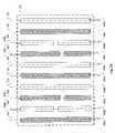
- FIG. 2Ais an illustration showing a splitting of the layout of FIG. 1 into two sub-layouts, in accordance with one embodiment of the present invention
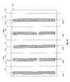
- FIG. 2Bis an illustration showing the first sub-layout as defined in the layout splitting of FIG. 2A , in accordance with one embodiment of the present invention
- FIG. 2Cis an illustration showing the second sub-layout as defined in the layout splitting of FIG. 2A , in accordance with one embodiment of the present invention
- FIG. 2Dis an illustration showing the splitting of the layout of FIG. 2A into three sub-layouts, in accordance with one embodiment of the present invention
- FIG. 3is an illustration showing a PCT processed version of the sub-layout of FIG. 2C , in accordance with one embodiment of the present invention
- FIGS. 4A-4Care illustrations showing possible sub-layout sequences for a layout that is split into three sub-layouts, in accordance with one embodiment of the present invention.
- FIG. 5Ais an illustration showing a gate level layout and metal 2 level layout for a cell, in accordance with one embodiment of the present invention.
- FIGS. 5B-5Eare illustrations showing different variants of the cell of FIG. 5A , in accordance with one embodiment of the present invention.
- FIG. 5F-5Gare illustrations showing placement of cell variants next to each other such that the sub-layout patterns for multiple levels extend across the cell boundaries, in accordance with one embodiment of the present invention
- FIG. 6Ais an illustration showing a non-segmented layout of a level of a cell, in accordance with one embodiment of the present invention.
- FIG. 6Bis an illustration showing a first non-segmented sub-layout including the linear-shaped layout features designated by the label A in FIG. 6A , in accordance with one embodiment of the present invention
- FIG. 6Cis an illustration showing a second non-segmented sub-layout including the linear-shaped layout features designated by the label B in FIG. 6A , in accordance with one embodiment of the present invention
- FIG. 6Dis an illustration showing a layout to be used for cutting the linear-shaped features as fabricated by the first and second non-segmented sub-layouts of FIGS. 6B and 6C , in accordance with one embodiment of the present invention
- FIG. 6Eis an illustration showing the level of the cell following the line cutting by the layout of FIG. 6D , in accordance with one embodiment of the present invention.
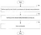
- FIG. 7is an illustration showing a flowchart of a method for defining a multiple patterned cell layout for use in an integrated circuit design, in accordance with one embodiment of the present invention.
- FIG. 8is an illustration showing a flowchart of a method for creating a cell library for multiple patterning of a chip layout, in accordance with one embodiment of the present invention.
- FIG. 9is an illustration showing a flowchart of a method for designing an integrated circuit for fabrication, in accordance with one embodiment of the present invention.
- One technique for resolving nano-scale layout features without further decreasing the illumination wavelength and without further increasing the numerical aperture NAis to utilize multiple patterning. More specifically, in multiple patterning, a given layout is split into two or more sub-layouts that are each exposed separately over the same area of the chip in the optical lithography process. Although the individual feature sizes in each of the sub-layouts may be small, i.e., nano-scale, a spacing between adjacent layout features in a given sub-layout is sufficiently large to enable resolution of the small layout features.
- a cellrepresents an abstraction of a logic function, and encapsulates lower-level integrated circuit layouts for implementing the logic function.
- a given logic functioncan be represented by multiple cell variations, wherein the cell variations may be differentiated by feature size, performance, and process compensation technique (PCT) processing.
- PCTprocess compensation technique
- multiple cell variations for a given logic functionmay be differentiated by power consumption, signal timing, current leakage, chip area, OPC, RET, etc.
- multiple cell variationsmay be differentiated by sub-layout sequence combination, as described herein.
- each cell descriptionincludes the layouts for the cell in each level of a chip, as required to implement the logic function of the cell. More specifically, a cell description includes layouts for the cell in each level of the chip extending from the substrate level up through a particular interconnect level.
- the dynamic array architecturerepresents a semiconductor device design paradigm in which linear-shaped layout features are defined along a regular-spaced virtual grate (or regular-spaced virtual grid) in a number of levels of a cell, i.e., in a number of levels of a semiconductor chip.
- the virtual grateis defined by a set of equally spaced, parallel virtual lines extending across a given level in a given chip area.
- the virtual gridis defined by a first set of equally spaced, parallel virtual lines extending across a given level in a given chip area in a first direction, and by a second set of equally spaced, parallel virtual lines extending across the given level in the given chip area in a second direction, where the second direction is perpendicular to the first direction.
- the virtual grate of a given levelis oriented to be substantially perpendicular to the virtual grate of an adjacent level.
- the virtual grate of a given levelis oriented to be either perpendicular or parallel to the virtual grate of an adjacent level.
- each linear-shaped layout feature of a given levelis substantially centered upon one of the virtual lines of the virtual grate associated with the given level.
- a linear-shaped layout featureis considered to be substantially centered upon a particular line of a virtual grate when a deviation in alignment between of the centerline of the linear-shaped layout feature and the particular line of the virtual grate is sufficiently small so as to not reduce a manufacturing process window from what would be achievable with a true alignment between of the centerline of the linear-shaped layout feature and the line of the virtual grate.
- the above-mentioned manufacturing process windowis defined by a lithographic domain of focus and exposure that yields an acceptable fidelity of the layout feature.
- the fidelity of a layout featureis defined by a characteristic dimension of the layout feature.
- the centerline of a given linear-shaped layout featureis defined as a virtual line that passes through the cross-sectional centroid of the linear-shaped layout feature at all points along its length, wherein the cross-sectional centroid of the linear-shaped layout feature at any given point along its length is the centroid of its vertical cross-section area at the given point.
- some linear-shaped layout features in a given levelmay not be centered upon a virtual line of the virtual grate associated with the given level.
- the linear-shaped layout featuresremain parallel to the virtual lines of the virtual grate, and hence parallel to the other linear-shaped layout features in the given level. Therefore, it should be understood that the various linear-shaped layout features defined in a layout of a given level are oriented to extend across the given level in a parallel manner.
- each linear-shaped layout featureis defined to be devoid of a substantial change in direction along its length.
- the lack of substantial change in direction of a linear-shaped layout featureis considered relative to the line of the virtual grate along which the linear-shaped layout feature is defined.
- a substantial change in direction of a linear-shaped layout featureexists when the width of the linear-shaped layout feature at any point thereon changes by more than 50% of the nominal width of the linear-shaped layout feature along its entire length.
- a substantial change in direction of a linear-shaped layout featureexists when the width of the linear-shaped layout feature changes from any first location on the linear-shaped layout feature to any second location on the linear-shaped layout feature by more that 50% of the linear-shaped layout feature width at the first location. Therefore, it should be appreciated that the dynamic array architecture specifically avoids the use of non-linear-shaped layout features, wherein a non-linear-shaped layout feature includes one or more bends within a plane of the associated level.
- the dynamic array architecturevariations in a vertical cross-section shape of an as-fabricated linear-shaped layout feature can be tolerated to an extent, so long as the variation in the vertical cross-section shape is predictable from a manufacturing perspective and does not adversely impact the manufacture of the given linear-shaped layout feature or its neighboring layout features.
- the vertical cross-section shapecorresponds to a cut of the as-fabricated linear-shaped layout feature in a plane perpendicular to the centerline of the linear-shaped layout feature.
- variation in the vertical cross-section of an as-fabricated linear-shaped layout feature along its lengthcan correspond to a variation in width along its length. Therefore, the dynamic array architecture also accommodates variation in the width of an as-fabricated linear-shaped layout feature along its length, so long as the width variation is predictable from a manufacturing perspective and does not adversely impact the manufacture of the linear-shaped layout feature or its neighboring layout features.
- different linear-shaped layout features within a given levelcan be designed to have the same width or different widths.
- the widths of a number of linear-shaped layout features defined along adjacent lines of a given virtual gratecan be designed such that the number of linear-shaped layout features contact each other so as to form a single linear-shaped layout feature having a width equal to the sum of the widths of the number of linear-shaped layout features.
- proximate ends of adjacent, co-aligned linear-shaped layout featuresmay be separated from each other by a substantially uniform gap. More specifically, adjacent ends of linear-shaped layout features defined along a common line of a virtual grate are separated by an end gap, and such end gaps within the level associated with the virtual grate may be defined to span a substantially uniform distance. Additionally, in one embodiment, a size of the end gaps is minimized within a manufacturing process capability so as to optimize filling of a given level with linear-shaped layout features.
- a levelcan be defined to have any number of virtual grate lines occupied by any number of linear-shaped layout features.
- a given levelcan be defined such that all lines of its virtual grate are occupied by at least one linear-shaped layout feature.
- a given levelcan be defined such that some lines of its virtual grate are occupied by at least one linear-shaped layout feature, and other lines of its virtual grate are vacant, i.e., not occupied by any linear-shaped layout features.
- any number of successively adjacent virtual grate linescan be left vacant.
- the occupancy versus vacancy of virtual grate lines by linear-shaped layout features in a given levelmay be defined according to a pattern or repeating pattern across the given level.
- vias and contactsare defined to interconnect a number of the linear-shaped layout features in various levels so as to form a number of functional electronic devices, e.g., transistors, and electronic circuits.
- Layout features for the vias and contactscan be aligned to virtual grid, wherein a specification of this virtual grid is a function of the specifications of the virtual grates associated with the various levels to which the vias and contacts will connect.
- a number of the linear-shaped layout features in various levelsform functional components of an electronic circuit.
- some of the linear-shaped layout features within various levelsmay be non-functional with respect to an electronic circuit, but are manufactured nonetheless so as to reinforce manufacturing of neighboring linear-shaped layout features. It should be understood that the dynamic array architecture is defined to enable accurate prediction of semiconductor device manufacturability with a high probability.
- the dynamic array architectureis defined by placement of linear-shaped layout features on a regular-spaced grate (or regular-spaced grid) in a number of levels of a cell, such that the linear-shaped layout features in a given level of the cell are oriented to be substantially parallel with each other in their traversal direction across the cell.
- each linear-shaped layout featureis defined to be devoid of a substantial change in direction relative to its traversal direction across the cell.
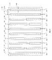
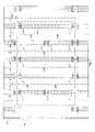
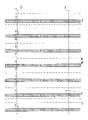
- FIG. 1is an illustration showing an exemplary layout for a level of a cell 101 defined in accordance with the dynamic array architecture, in accordance with one embodiment of the present invention.
- a number of linear-shaped layout features 105are placed along virtual lines 103 of a virtual grate associated with the level of the cell 101 .
- the virtual grateis defined by a pitch 107 representing a perpendicular spacing between adjacent virtual lines 103 .
- each of the linear-shaped layout features 105is defined to have a width 109 . It should be understood, however, that in other embodiments various linear-shaped layout features in a given level of a cell may be defined to have a number of different widths.
- the pitch 107 of the virtual grate, the width 109 of the linear-shaped features 105 , and the occupancy of the virtual grate by the linear-shaped layout features 105combine such that the layout of the level of the cell 101 is outside a fabrication capability of a given semiconductor fabrication process. Therefore, to facilitate fabrication of the level of the cell 101 , the layout can be split into a number of sub-layouts, such that each of the number of linear-shaped layout features 105 in the layout is allocated to any one of the number of sub-layouts, and such that each sub-layout is independently fabricatable within the fabrication capability of the given semiconductor fabrication process.
- a layout including linear-shaped layout features defined in accordance with the dynamic array architectureis split by allocating sidewardly adjacent layout features to different sub-layouts. It should be understood that allocation of sidewardly adjacent layout features to different sub-layouts can be applied with any number of sub-layouts. For example, in the case of double patterning in which two sub-layouts are used, every other layout feature in the layout for the level of the cell is allocated to a common sub-layout. In this case, identification of every other layout feature is made in accordance with a direction perpendicular to a traversal direction of the layout features across the cell.
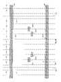
- FIG. 2Ais an illustration showing a splitting of the layout of FIG. 1 into two sub-layouts, in accordance with one embodiment of the present invention.
- FIG. 2Ais an example of double-patterning.
- a first sub-layout in FIG. 2Aincludes the layout features 105 A.
- a second sub-layout in FIG. 2Aincludes the layout features 105 B. Therefore, the layout is split such that sidewardly adjacent layout features are allocated to different sub-layouts. More specifically, every other sidewardly adjacent layout feature is allocated to a common sub-layout.
- each of the multiple linear-shaped layout featuresis allocated to the same sub-layout.
- each layout feature on a given virtual grate lineis allocated to the same sub-layout.
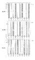
- FIG. 2Bis an illustration showing the first sub-layout as defined in the layout splitting of FIG. 2A .
- FIG. 2Cis an illustration showing the second sub-layout as defined in the layout splitting of FIG. 2A . It should be understood that each of the first and second sub-layouts of FIGS. 2B and 2C are to fabricated separately on the chip.
- adjacent linear-shaped layout features 105 Aare separated by a distance 111 .
- adjacent linear-shaped layout features 105 Bare also separated by the distance 111 .
- the distance 111is sufficiently large such that each of the first and second sub-layouts is independently fabricatable within the fabrication capability of a given semiconductor fabrication process, then use of two sub-layouts is adequate. However, if the distance 111 is not sufficiently large to enable independent fabrication of the first and second sub-layouts, the layout of FIG. 2A could be split into more than two sub-layouts.
- FIG. 2Dis an illustration showing the splitting of the layout of FIG. 2A into three sub-layouts.
- a first sub-layout in FIG. 2Dincludes the layout features 105 A.
- a second sub-layout in FIG. 2Dincludes the layout features 105 B.
- a third sub-layout in FIG. 2Dincludes the layout features 105 C. It should be appreciated that the distance 115 between adjacent layout features in each of the three sub-layouts of FIG. 2D is larger than the distance 111 in the two sub-layouts of FIGS. 2B and 2C .
- each of the three sub-layouts having the layout feature separation distance 115should be more likely to fall within the fabrication capability of a given semiconductor fabrication process, as compared to the two sub-layouts having the layout feature separation distance 111 .
- the layout feature separation distance 115by splitting the layout of a given level of a cell into multiple sub-layouts, it is possible to resolve smaller layout feature sizes.
- a given layoutcan be split into essentially any number of sub-layouts, wherein each sub-layout for the given level of the cell is to be fabricated separately.
- a layout for a given level of a cellcan be split into a number of sub-layouts based on layout feature function, layout feature location, or a combination thereof.
- layout features sharing a common electrical functioncan be allocated to a common sub-layout.
- layout features for active region contactscan be commonly allocated to one sub-layout
- layout features for gate contactscan be commonly allocated to another sub-layout.
- layout features for viascan be allocated to sub-layouts in accordance with alternating rows and/or columns of the virtual grid upon which the via layout features are placed.
- each of the sub-layoutscan be process compensation technique (PCT) processed separately, as each of the sub-layouts will be exposed separately during the lithography process.
- PCTprocess compensation technique
- ICintegrated circuit
- RETresolution enhancement techniques
- CMPchemical mechanical planarization
- FIG. 3is an illustration showing a PCT processed version of the sub-layout of FIG. 2C , in accordance with one embodiment of the present invention.
- a number of OPC shapes 117are placed at various ends of the linear-shaped layout features 105 B as part of the PCT processing of the sub-layout.
- a lithographic buffer region (“litho-buffer” hereafter) 119is defined around the cell 101 to simulate a chip environment in which the sub-layout for the level of the cell 101 may be placed and fabricated.
- a litho-buffer associated with a given sub-layout for a cell levelis defined to include a number of features that simulate the neighborhood in which the sub-layout for the cell level will be placed during fabrication on the chip.
- the size of the litho-buffer for a given cell levelis defined by the outward extent of the litho-buffer from the cell. For example, in FIG. 3 , the litho-buffer 119 extends outward from the cell 101 to a boundary 121 .
- the size of the litho-buffer for a given cell levelis set such that the litho-buffer covers an area capable of lithographically influencing fabrication of the sub-layout in the given cell level.
- a litho-buffer for a cell level defined in accordance with the dynamic array architecturecan be defined by surrounding the cell level with duplicate instantiations of itself.
- the litho-buffer for the cell level defined in accordance with the dynamic array architecturecan be defined in a more generalized manner to include a “blanket” of linear features which approximate those present in the cell level.
- the blanket of linear featurescan be defined to include a number of linear features placed according to an extension of the virtual grate/virtual grid utilized within the cell level, and according to an extension of the sub-layout of the cell level.
- PCT correctionsmay be primarily intended to maintain the line width of each linear-shaped layout feature in critical regions. Therefore, the PCT corrections can be relatively simple, such as one-dimensional corrections similar to those provided by the OPC shapes 117 in FIG. 3 . Further description of PCT processing of a given level of a cell can be found in co-pending U.S. patent application Ser. No. 12/033,807, which is incorporated in its entirety herein by reference.
- a particular sub-layout sequenceFor each layout that is split into a number of sub-layouts, a particular sub-layout sequence can be specified.
- the sub-layout sequenceis defined by allocating an edge layout feature of the layout to a particular sub-layout and by allocating sidewardly adjacent layout features, relative to a direction extending across the layout away from the edge layout feature, according to a fixed ordering of the number of sub-layouts. Because each sub-layout sequence is based on allocation of an edge layout feature to a particular sub-layout, the number of possible sub-layout sequences is equal to the number of sub-layouts into which the layout is split.
- FIGS. 4A-4Care illustrations showing possible sub-layout sequences for a layout that is split into three sub-layouts, in accordance with one embodiment of the present invention.
- the three sub-layoutsare designed by the letters A, B, and C, respectively.
- the fixed ordering of the number of sub-layoutsis specified as A-B-C. Therefore, FIG. 4A shows a first sub-layout sequence in which the left edge layout feature 401 is allocated to sub-layout A, and the fixed ordering of sub-layouts (A-B-C) is applied to sidewardly adjacent features based on the allocation of the left edge layout feature 401 to sub-layout A.
- FIG. 4Bshows a second sub-layout sequence in which the left edge layout feature 401 is allocated to sub-layout B, and the fixed ordering of sub-layouts (A-B-C) is applied to sidewardly adjacent features based on the allocation of the left edge layout feature 401 to sub-layout B.
- FIG. 4Cshows a third sub-layout sequence in which the left edge layout feature 401 is allocated to sub-layout C, and the fixed ordering of sub-layouts (A-B-C) is applied to sidewardly adjacent features based on the allocation of the left edge layout feature 401 to sub-layout C.
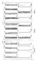
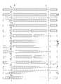
- FIG. 5Ais an illustration showing a gate level layout and metal 2 level layout for a cell 501 , in accordance with one embodiment of the present invention.
- gate level layout features 503 and metal 2 level layout features 505are abbreviated in their traversal direction across the cell 501 to avoid obscuring each other.
- each gate level feature 503 and each metal 2 level feature 505extends across the cell 501 , as indicated by arrows 507 .
- the gate level layoutis split into two sub-layouts.
- the metal 2 level layoutis split into two sub-layouts.
- FIGS. 5B-5Eare illustrations showing different variants of the cell 501 .
- the gate level layoutis split into two sub-layouts identified as 503 A and 503 B, respectively.
- the metal 2 level layoutis split into two sub-layouts identified as 505 A and 505 B, respectively. Because the gate level layout is split into two sub-layouts, there are two possible sub-layout sequences for the gate level, i.e., 503 A- 503 B, and 503 B- 503 A.
- the metal 2 level layoutis split into two sub-layouts, there are two possible sub-layout sequences for the metal 2 level layout, i.e., 505 A- 505 B, and 505 B- 505 A. Therefore, in considering the combination of sub-layout sequences across the levels of the cell 501 , four variants of the cell 501 can be generated based on unique sub-layout sequence combinations.
- FIG. 5Ashows a cell variant 501 A in which the combination of sub-layout sequences applied across the levels of the cell 501 is defined by 503 A- 503 B for the gate level and 505 A- 505 B for the metal 2 level.
- FIG. 5Bshows a cell variant 501 B in which the combination of sub-layout sequences applied across the levels of the cell 501 is defined by 503 B- 503 A for the gate level and 505 A- 505 B for the metal 2 level.
- FIG. 5Cshows a cell variant 501 C in which the combination of sub-layout sequences applied across the levels of the cell 501 is defined by 503 A- 503 B for the gate level and 505 B- 505 A for the metal 2 level.
- FIG. 5Dshows a cell variant 501 D in which the combination of sub-layout sequences applied across the levels of the cell 501 is defined by 503 B- 503 A for the gate level and 505 B- 505 A for the metal 2 level.
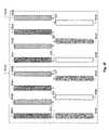
- FIG. 5Fis an illustration showing placement of cell variant 501 B next to cell variant 501 A such that the sub-layout patterns for the gate level and the metal 2 level extend across the cell boundaries.
- FIG. 5Gis an illustration showing placement of cell variant 501 D next to cell variant 501 C such that the sub-layout patterns for the gate level and the metal 2 level extend across the cell boundaries.
- the splitting of various layouts of a cell into multiple sub-layoutscan be built into the cell library.
- the dynamic array architectureit is possible to split a layout of a given cell level into multiple sub-layouts as the cell library is being created.
- each variant of a given cellcan be stored in the cell library, wherein each cell variant corresponds to a unique combination of sub-layout sequences applied across the levels of the given cell.
- appropriate cell variantscan be selected from the cell library for placement on the chip to ensure that chip-level layout patterns are maintained across the chip.
- a router used to place and route the chipis defined to understand how the various layouts for each level of the chip are split, thereby enabling placement of cells such that sub-layouts for a given level align and extend across cell boundaries.
- chip-wide layout splitting of a given levelis accomplished by placing appropriate cell variants during the chip place and route process, without considering the chip-wide layout as a whole.
- chip-wide layout splitting of a given levelcan be performed following the chip place and route process. It should be appreciated that in this embodiment, definition of the various cells in accordance with the dynamic array architecture serves to significantly improve the ease by which the chip-wide layout can be split.
- Each chip-wide sub-layout for a given levelis defined on a respective mask.
- the masks for the various sub-layouts of each level of the chipare stored as layout data files to be sent to the mask fabrication facility.
- the layout data filescan be formatted as GDS II (Graphic Data System) database files, OASIS (Open Artwork System Interchange Standard) database files, or any other type of date file format that can be understood by the mask fabrication facility.
- FIG. 6Ais an illustration showing a non-segmented layout of a level of a cell 601 , in accordance with one embodiment of the present invention.
- each linear-shaped layout featureis defined to extend continuously across the layout, including across cell boundaries.
- the non-segmented layoutcan be split into a number of sub-layouts.
- the non-segmented layoutis split into two sub-layouts designated by labels A and B, respectively.
- FIG. 6Bis an illustration showing a first non-segmented sub-layout including the linear-shaped layout features designated by the label A.
- FIG. 6Cis an illustration showing a second non-segmented sub-layout including the linear-shaped layout features designated by the label B.
- Each of the first and second non-segmented sub-layoutsare fabricated separately on the same level of the chip.
- FIG. 6Dis an illustration showing a layout to be used for cutting the linear-shaped features as fabricated by the first and second non-segmented sub-layouts of FIGS. 6B and 6C .
- the layout of FIG. 6Dincludes layout features 609 - 1 and 609 - 2 for line cutting at the cell 601 boundary. Also, layout features 609 - 3 through 609 - 6 are provided for segmentation of linear features within the cell 601 .
- the layout of FIG. 6Dis defined to cut the linear-shaped features as fabricated by the first and second non-segmented sub-layouts of FIGS. 6B and 6C , so as to enable electrical connectivity necessary for the logic function of the cell 601 .
- FIG. 6Eis an illustration showing the level of the cell 601 following the line cutting by the layout of FIG. 6D .
- a set of masksare generated for fabricating a common level of a semiconductor chip in accordance with the line cutting technique illustrated by FIGS. 6A-6E .
- the set of masksincludes a first mask having an area defined in accordance with a dynamic array architecture to include a first number of linear layout features defined to extend continuously across the area of the first mask.
- the first number of linear layout featuresare commonly oriented.
- each of the first number of linear layout featuresis devoid of a substantial change in traversal direction across the first mask.
- the first number of linear layout featuresform a first sub-layout, wherein the first sub-layout defines a first portion of one or more cells.
- the set of masksalso includes a second mask having an area defined in accordance with the dynamic array architecture to include a second number of linear layout features defined to extend continuously across the area of the second mask.
- the second number of linear layout featuresare commonly oriented with the first number of linear layout features of the first mask.
- Each of the second number of linear layout featuresis devoid of a substantial change in traversal direction across the second mask.
- the area of the second mask defined in accordance with the dynamic array architectureis to be aligned with the area of the first mask defined in accordance with the dynamic array architecture, thereby causing the second number of linear layout features to be interleaved with the first number of linear layout features.
- the second number of linear layout featuresform a second sub-layout, wherein the second sub-layout defines a second portion of the one or more cells.
- the set of masksalso includes a third mask having an area defined to include a third number of linear layout features.
- the third number of linear layout featuresare oriented to be substantially perpendicular to both the first and second number of linear layout features, when the area of the third mask is aligned with the areas of the first and second masks.
- the third number of linear layout featuresare defined to provide for cutting of a portion of the first and second number of linear layout features, so as to segment the first and second number of linear layout features to enable electrical connectivity necessary for the logic function of each of the one or more cells. It should be understood that enumeration of the above-mentioned masks as “first,” “second,” and “third” is provided for purposes of mask differentiation and is not intended to convey an absolute number of a given mask.
- the non-segmented layout of FIG. 6Acan be formed using a self-aligned double patterning (SADP) process, in lieu of using the separate sub-layout masks of FIGS. 6B and 6C .
- the cutting layout, i.e., cut mask, of FIG. 6Dcan be used to cut the non-segmented layout features formed using the SADP process, so as to yield the layout shown in FIG. 6E .
- the SADP process in this embodimentcan be extended to a self-aligned quadruple patterning (SAQP) process, and beyond.
- SAQPself-aligned quadruple patterning
- multiple patterningis performed by separately loading different sub-layouts for a given level into a stepper. In this embodiment, alignment between the layout features of the different sub-layouts should be performed accurately to ensure proper spacing between layout features in the given level.
- multiple patterningis performed using a double exposure technique in which multiple sub-layouts can be exposed on a wafer with a single alignment of the wafer to the scanner optical column. In one embodiment, the double exposure technique can be performed with each of multiple sub-layouts on a respective mask. In another embodiment, if the chip size allows, the double exposure technique can be performed with each of the multiple sub-layouts on the same mask, with an offset between the sub-layouts.
- use of the dynamic array architectureassists with alignment of sub-layouts when fabricating a given level of the chip. For example, in one embodiment, alignment in the direction along the length of the linear-shaped layout features may be more relaxed relative to alignment in the perpendicular direction extending between layout features. Also, given the parallelism of the linear-shaped layout features in a given level, proper rotational alignment of the sub-layouts for the given level may be more easily identified.
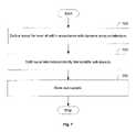
- FIG. 7is an illustration showing a flowchart of a method for defining a multiple patterned cell layout for use in an integrated circuit design, in accordance with one embodiment of the present invention.
- the methodincludes an operation 701 for defining a layout for a level of a cell, wherein the layout is defined in accordance with a dynamic array architecture to include a number of layout features.
- the number of layout featuresare linear-shaped and commonly oriented.
- the methodalso includes an operation 703 for splitting the layout into a number of sub-layouts for the level of the cell, such that each of the number of layout features in the layout is allocated to any one of the number of sub-layouts, and such that each sub-layout is independently fabricatable.
- a size of the layout features and a spacing between adjacent layout features in the layout for the level of the cell, prior to the splitting of operation 703are outside a fabrication capability of a given semiconductor fabrication process.
- the size of the layout features and a spacing between adjacent layout features in each sub-layout for the level of the cell, after the splitting of operation 703are within the fabrication capability of the given semiconductor fabrication process.
- sidewardly adjacent layout features in the layout for the level of the cellare allocated to different sub-layouts.
- layout features sharing a common electrical function in the layout for the level of the cellare allocated to a common sub-layout.
- layout features for active region contactsare commonly allocated to one sub-layout, and layout features for gate contacts are commonly allocated to another sub-layout.
- every other layout feature in the layout for the level of the cellis allocated to a common sub-layout, wherein an identification of every other layout feature is made in accordance with a direction perpendicular to a traversal direction of the layout features across the cell.
- the methodfurther includes an operation 705 for storing the number of sub-layouts for the level of the cell on a computer readable medium. It should be understood that each sub-layout for the level of the cell is to be fabricated separately within a common area of a chip. Additionally, operations 701 - 705 are repeated for a number of levels of the cell.
- the methodcan also include an operation for defining a sub-layout sequence for the level of the cell by allocating an edge layout feature of the level of the cell to a particular sub-layout, and by allocating sidewardly adjacent layout features (relative to a direction extending across the level of the cell away from the edge layout feature) according to a fixed ordering of the number of sub-layouts for the level of the cell.
- the methodcan further include an operation for generating a number of variants of the cell, wherein each variant of the cell is defined by a unique combination of sub-layout sequences applied across levels of the cell.
- Each variant of the cellcan be stored in a cell library on a computer readable medium.
- PCT processingcan be performed on each sub-layout to generate a PCT processed version each sub-layout.
- the PCT processed version of each sub-layoutcan be stored in a cell library on a computer readable medium.
- the PCT processingis performed on a given sub-layout by defining a lithographic buffer region around the given sub-layout.
- the lithographic buffer regionis defined to include a number of features that simulate a neighborhood of the given sub-layout around the cell when placed on a chip.
- FIG. 8is an illustration showing a flowchart of a method for creating a cell library for multiple patterning of a chip layout, in accordance with one embodiment of the present invention.
- the methodincludes an operation 801 for defining a cell to include a number of levels having a respective linear layout defined in accordance with a dynamic array architecture.
- the methodalso includes an operation 803 in which, for one or more select levels of the cell, the respective linear layout is split into a number of sub-layouts, such that each of the number of layout features in the respective linear layout is allocated to any one of the number of sub-layouts, and such that each sub-layout is independently fabricatable.
- the methodfurther includes an operation 805 for storing a definition of the cell in a cell library on a computer readable medium.
- the definition of the cellincludes the number of sub-layouts associated with each of the select levels of the cell.
- the method of FIG. 8further includes an operation for generating a number of variants of the cell.
- Each variant of the cellis defined by a unique combination of sub-layout sequences applied across the select levels of the cell.
- a sub-layout sequence for a given level of the cellis defined by allocating an edge layout feature of the given level of the cell to a particular sub-layout, and by allocating sidewardly adjacent layout features (relative to a direction extending across the given level of the cell away from the edge layout feature) according to a fixed ordering of the number of sub-layouts for the given level of the cell.
- each variant of the cellis stored in the cell library on the computer readable medium.
- the method of FIG. 8can include an operation for PCT processing each sub-layout to generate a PCT processed version of each sub-layout.
- the PCT processed version of each sub-layoutis stored in the cell library on the computer readable medium.
- each linear layoutprior to being split into the number of sub-layouts in operation 803 , each linear layout is outside a fabrication capability of a given semiconductor fabrication process. However, in this embodiment, after splitting of the linear layout in operation 803 , each of the number of sub-layouts is within the fabrication capability of the given semiconductor fabrication process.
- FIG. 9is an illustration showing a flowchart of a method for designing an integrated circuit for fabrication, in accordance with one embodiment of the present invention.
- the methodincludes an operation 901 for placing a plurality of cells together on a chip layout to satisfy a netlist of the integrated circuit.
- the plurality of cellsare selected from a cell library for multiple patterning of the chip layout.
- Each of the plurality of cellsincludes a common level having a respective linear layout defined in accordance with a dynamic array architecture.
- each linear layoutis split into a number of sub-layouts, such that each layout feature in each linear layout is allocated to any one of the number of sub-layouts, and such that layout features allocated to a given sub-layout form a consistent pattern within the common level of a given cell.
- the plurality of cellsare placed together in operation 901 such that the consistent pattern of layout features formed by the given sub-layout within the common level extends in an uninterrupted manner across the plurality of cells.
- the extension of the consistent pattern of layout features formed by the given sub-layout across the plurality of cellsdefines a portion of a chip-wide mask layout for the common level.
- each sub-layoutis defined on a separate chip-wide mask layout for the common level, wherein each chip-wide mask layout is to be independently fabricated in a co-aligned manner on the common level.
- the methodfurther includes an operation 903 for storing the chip-wide mask layout for the common level on a computer readable medium.
- the invention described hereincan be embodied as computer readable code on a computer readable medium.
- the computer readable mediumis any data storage device that can store data which can be thereafter be read by a computer system. Examples of the computer readable medium include hard drives, network attached storage (NAS), read-only memory, random-access memory, CD-ROMs, CD-Rs, CD-RWs, magnetic tapes, and other optical and non-optical data storage devices.
- the computer readable mediumcan also be distributed over a network coupled computer systems so that the computer readable code is stored and executed in a distributed fashion.
- GUIgraphical user interface
- implemented as computer readable code on a computer readable mediumcan be developed to provide a user interface for performing any embodiment of the present invention.
Landscapes
- Engineering & Computer Science (AREA)
- Physics & Mathematics (AREA)
- Computer Hardware Design (AREA)
- Theoretical Computer Science (AREA)
- General Physics & Mathematics (AREA)
- General Engineering & Computer Science (AREA)
- Evolutionary Computation (AREA)
- Geometry (AREA)
- Computer Networks & Wireless Communication (AREA)
- Architecture (AREA)
- Design And Manufacture Of Integrated Circuits (AREA)
Abstract
Description
- This application claims priority under 35 U.S.C. 119(e) to U.S. Provisional Patent Application No. 60/892,982, filed Mar. 5, 2007, entitled “Integrated Circuit Cell Library Suitable for Multiple Patterning.” The disclosure of the above-identified provisional patent application is incorporated herein by reference.
- This application is also related to U.S. patent application Ser. No. 11/683,402, filed on Mar. 7, 2007, and entitled “Dynamic Array Architecture.” This application is also related to U.S. patent application Ser. No. 12/013,342, filed on Jan. 11, 2008, and entitled “Semiconductor Device with Dynamic Array Section.” This application is also related to U.S. patent application Ser. No. 12/013,356, filed on Jan. 11, 2008, and entitled “Methods for Designing Semiconductor Device with Dynamic Array Section.” This application is also related to U.S. patent application Ser. No. 12/013,366, filed on Jan. 11, 2008, and entitled “Methods for Defining Dynamic Array Section with Manufacturing Assurance Halo and Apparatus Implementing the Same.” This application is also related to U.S. patent application Ser. No. 12/033,807, filed on Feb. 19, 2008, and entitled “Integrated Circuit Cell Library with Cell-Level Process Compensation Technique (PCT) Application and Associated Methods.” The disclosures of the above-identified patent applications are incorporated herein by reference.
- In modern semiconductor fabrication, optical lithography is used to pattern layout features onto a semiconductor wafer. Current step-and-repeat optical lithography systems and step-scan-and-repeat optical lithography systems use illumination sources with wavelengths of 365 nanometers (nm) (Hg I-line), 248 nm (KrF B-X excimer laser), and 193 nm (ArF B-X excimer laser). Historically, it has been possible to use illumination wavelengths larger than the layout feature sizes to be patterned. However, as layout feature sizes continue to decrease without a corresponding decrease in available illumination wavelength, the difference between the smallest wavelength and smallest layout feature size has become too large for successful lithographic rendering of the features. For example, lithographers are having great difficulty patterning 65 nm layout feature sizes with the 193 nm illumination source. Moreover, layout feature sizes are expected to continue to decrease from 65 nm to 45 nm, and on to 32 nm.
- Lithographers use the following formula from Lord Rayleigh to estimate the optical system capability: resolution (half-pitch)=k1λ/NA, where k1is a fitting variable roughly corresponding to a process window, λ is the illumination wavelength, and NA is the numerical aperture of the lithographic system. When the wavelength λ was larger than the half-pitch, typical values for k1were over 0.50. Because the feature size has been decreasing by a factor of 0.7 for each technology node, the value of k1has been steadily decreasing for each technology node, while the wavelength λ has been constant, and the NA has been increasing by only 1.1 to 1.2 per technology node step. Additionally, for a NA greater than about 0.93, immersion systems are needed in which water replaces air as the medium between the final lens and the photoresist on the wafer. These immersion systems are expected to support a NA up to about 1.35, with no clear, cost-effective solution thereafter.
- In view of the foregoing, a solution is needed to enable patterning of nano-scale feature sizes without having to further decrease illumination wavelength λ and/or further increase numerical aperture NA.
- In one embodiment, a method is disclosed for defining a multiple patterned cell layout for use in an integrated circuit design. The method includes an operation for defining a layout for a level of a cell. The layout is defined in accordance with a dynamic array architecture to include a number of layout features. The number of layout features are linear-shaped and commonly oriented. The method also includes an operation for splitting the layout into a number of sub-layouts for the level of the cell, such that each of the number of layout features in the layout is allocated to any one of the number of sub-layouts. The layout is split such that each sub-layout is independently fabricatable. The method further includes an operation for storing the number of sub-layouts for the level of the cell on a computer readable medium.
- In another embodiment, a method is disclosed for creating a cell library for multiple patterning of a chip layout. The method includes an operation for defining a cell to include a number of levels having a respective linear layout defined in accordance with a dynamic array architecture. The dynamic array architecture is defined by layout features that are linear-shaped and commonly oriented. The cell represents an abstraction of a logic function and encapsulates lower-level integrated circuit layouts for implementing the logic function. For one or more select levels of the cell, the method includes an operation for splitting the respective linear layout into a number of sub-layouts, such that each of the number of layout features in the respective linear layout is allocated to any one of the number of sub-layouts, and such that each sub-layout is independently fabricatable. The method further includes an operation for storing a definition of the cell in a cell library on a computer readable medium. The definition of the cell includes the number of sub-layouts associated with each of the select levels of the cell.
- In another embodiment, a method is disclosed for designing an integrated circuit for fabrication. In the method, a plurality of cells are placed together on a chip layout to satisfy a netlist of the integrated circuit. The plurality of cells are selected from a cell library for multiple patterning of the chip layout. Each of the plurality of cells includes a common level having a respective linear layout defined in accordance with a dynamic array architecture. The dynamic array architecture is defined by layout features that are linear-shaped and commonly oriented. Each linear layout is split into a number of sub-layouts, such that each layout feature in each linear layout is allocated to any one of the number of sub-layouts. Layout features allocated to a given sub-layout form a consistent pattern within the common level of a given cell. The plurality of cells are placed together such that the consistent pattern of layout features, as formed by the given sub-layout within the common level, extends in an uninterrupted manner across the plurality of cells. The extension of the consistent pattern of layout features formed by the given sub-layout across the plurality of cells defines a portion of a chip-wide mask layout for the common level. The method also includes an operation for storing the chip-wide mask layout for the common level on a computer readable medium.
- In another embodiment, a set of masks for fabricating a common level of a semiconductor chip is disclosed. The set of masks includes a first mask having an area defined in accordance with a dynamic array architecture to include a first number of linear layout features. The first number of linear layout features are commonly oriented. Also, each of the first number of linear layout features is devoid of a substantial change in traversal direction across the first mask. The first number of linear layout features form a first sub-layout that defines a first portion of one or more cells. Each of the one or more cells represents an abstraction of a logic function and encapsulates lower-level integrated circuit layouts for implementing the logic function. The set of masks also includes a second mask having an area defined in accordance with the dynamic array architecture to include a second number of linear layout features. The second number of linear layout features are commonly oriented with the first number of linear layout features. Also, each of the second number of linear layout features is devoid of a substantial change in traversal direction across the second mask. The area of the second mask defined in accordance with the regular architecture is to be aligned with the area of the first mask defined in accordance with the regular architecture. The second number of linear layout features form a second sub-layout which defines a second portion of the one or more cells.
- Other aspects and advantages of the invention will become more apparent from the following detailed description, taken in conjunction with the accompanying drawings, illustrating by way of example the present invention.
FIG. 1 is an illustration showing an exemplary layout for a level of a cell defined in accordance with the dynamic array architecture, in accordance with one embodiment of the present invention;FIG. 2A is an illustration showing a splitting of the layout ofFIG. 1 into two sub-layouts, in accordance with one embodiment of the present invention;FIG. 2B is an illustration showing the first sub-layout as defined in the layout splitting ofFIG. 2A , in accordance with one embodiment of the present invention;FIG. 2C is an illustration showing the second sub-layout as defined in the layout splitting ofFIG. 2A , in accordance with one embodiment of the present invention;FIG. 2D is an illustration showing the splitting of the layout ofFIG. 2A into three sub-layouts, in accordance with one embodiment of the present invention;FIG. 3 is an illustration showing a PCT processed version of the sub-layout ofFIG. 2C , in accordance with one embodiment of the present invention;FIGS. 4A-4C are illustrations showing possible sub-layout sequences for a layout that is split into three sub-layouts, in accordance with one embodiment of the present invention;FIG. 5A is an illustration showing a gate level layout and metal 2 level layout for a cell, in accordance with one embodiment of the present invention;FIGS. 5B-5E are illustrations showing different variants of the cell ofFIG. 5A , in accordance with one embodiment of the present invention;FIG. 5F-5G are illustrations showing placement of cell variants next to each other such that the sub-layout patterns for multiple levels extend across the cell boundaries, in accordance with one embodiment of the present invention;FIG. 6A is an illustration showing a non-segmented layout of a level of a cell, in accordance with one embodiment of the present invention;FIG. 6B is an illustration showing a first non-segmented sub-layout including the linear-shaped layout features designated by the label A inFIG. 6A , in accordance with one embodiment of the present invention;FIG. 6C is an illustration showing a second non-segmented sub-layout including the linear-shaped layout features designated by the label B inFIG. 6A , in accordance with one embodiment of the present invention;FIG. 6D is an illustration showing a layout to be used for cutting the linear-shaped features as fabricated by the first and second non-segmented sub-layouts ofFIGS. 6B and 6C , in accordance with one embodiment of the present invention;FIG. 6E is an illustration showing the level of the cell following the line cutting by the layout ofFIG. 6D , in accordance with one embodiment of the present invention;FIG. 7 is an illustration showing a flowchart of a method for defining a multiple patterned cell layout for use in an integrated circuit design, in accordance with one embodiment of the present invention;FIG. 8 is an illustration showing a flowchart of a method for creating a cell library for multiple patterning of a chip layout, in accordance with one embodiment of the present invention; andFIG. 9 is an illustration showing a flowchart of a method for designing an integrated circuit for fabrication, in accordance with one embodiment of the present invention.- In the following description, numerous specific details are set forth in order to provide a thorough understanding of the present invention. It will be apparent, however, to one skilled in the art that the present invention may be practiced without some or all of these specific details. In other instances, well known process operations have not been described in detail in order not to unnecessarily obscure the present invention.
- One technique for resolving nano-scale layout features without further decreasing the illumination wavelength and without further increasing the numerical aperture NA is to utilize multiple patterning. More specifically, in multiple patterning, a given layout is split into two or more sub-layouts that are each exposed separately over the same area of the chip in the optical lithography process. Although the individual feature sizes in each of the sub-layouts may be small, i.e., nano-scale, a spacing between adjacent layout features in a given sub-layout is sufficiently large to enable resolution of the small layout features.
- It should be appreciated that multiple patterning can be quite difficult in traditional random logic patterns and associated cell libraries because of their two-dimensionally varying nature, i.e., with layout features having bends and forks. Additionally, there can be complex issues associated with splitting of two-dimensionally varying patterns, such as phase shifting conflicts. However, use of a cell library defined in accordance with a dynamic array architecture enables straightforward splitting of a layout into multiple sub-layouts to be used for lithographic exposure.
- A cell, as referenced herein, represents an abstraction of a logic function, and encapsulates lower-level integrated circuit layouts for implementing the logic function. It should be understood that a given logic function can be represented by multiple cell variations, wherein the cell variations may be differentiated by feature size, performance, and process compensation technique (PCT) processing. For example, multiple cell variations for a given logic function may be differentiated by power consumption, signal timing, current leakage, chip area, OPC, RET, etc. Additionally, multiple cell variations may be differentiated by sub-layout sequence combination, as described herein. It should also be understood that each cell description includes the layouts for the cell in each level of a chip, as required to implement the logic function of the cell. More specifically, a cell description includes layouts for the cell in each level of the chip extending from the substrate level up through a particular interconnect level.
- The dynamic array architecture represents a semiconductor device design paradigm in which linear-shaped layout features are defined along a regular-spaced virtual grate (or regular-spaced virtual grid) in a number of levels of a cell, i.e., in a number of levels of a semiconductor chip. The virtual grate is defined by a set of equally spaced, parallel virtual lines extending across a given level in a given chip area. The virtual grid is defined by a first set of equally spaced, parallel virtual lines extending across a given level in a given chip area in a first direction, and by a second set of equally spaced, parallel virtual lines extending across the given level in the given chip area in a second direction, where the second direction is perpendicular to the first direction. In one embodiment, the virtual grate of a given level is oriented to be substantially perpendicular to the virtual grate of an adjacent level. However, in other embodiments, the virtual grate of a given level is oriented to be either perpendicular or parallel to the virtual grate of an adjacent level.
- In one embodiment, each linear-shaped layout feature of a given level is substantially centered upon one of the virtual lines of the virtual grate associated with the given level. A linear-shaped layout feature is considered to be substantially centered upon a particular line of a virtual grate when a deviation in alignment between of the centerline of the linear-shaped layout feature and the particular line of the virtual grate is sufficiently small so as to not reduce a manufacturing process window from what would be achievable with a true alignment between of the centerline of the linear-shaped layout feature and the line of the virtual grate.
- In one embodiment, the above-mentioned manufacturing process window is defined by a lithographic domain of focus and exposure that yields an acceptable fidelity of the layout feature. In one embodiment, the fidelity of a layout feature is defined by a characteristic dimension of the layout feature. Also, it should be understood that the centerline of a given linear-shaped layout feature is defined as a virtual line that passes through the cross-sectional centroid of the linear-shaped layout feature at all points along its length, wherein the cross-sectional centroid of the linear-shaped layout feature at any given point along its length is the centroid of its vertical cross-section area at the given point.
- In another embodiment, some linear-shaped layout features in a given level may not be centered upon a virtual line of the virtual grate associated with the given level. However, in this embodiment, the linear-shaped layout features remain parallel to the virtual lines of the virtual grate, and hence parallel to the other linear-shaped layout features in the given level. Therefore, it should be understood that the various linear-shaped layout features defined in a layout of a given level are oriented to extend across the given level in a parallel manner.
- Also, in the dynamic array architecture, each linear-shaped layout feature is defined to be devoid of a substantial change in direction along its length. The lack of substantial change in direction of a linear-shaped layout feature is considered relative to the line of the virtual grate along which the linear-shaped layout feature is defined. In one embodiment, a substantial change in direction of a linear-shaped layout feature exists when the width of the linear-shaped layout feature at any point thereon changes by more than 50% of the nominal width of the linear-shaped layout feature along its entire length. In another embodiment, a substantial change in direction of a linear-shaped layout feature exists when the width of the linear-shaped layout feature changes from any first location on the linear-shaped layout feature to any second location on the linear-shaped layout feature by more that 50% of the linear-shaped layout feature width at the first location. Therefore, it should be appreciated that the dynamic array architecture specifically avoids the use of non-linear-shaped layout features, wherein a non-linear-shaped layout feature includes one or more bends within a plane of the associated level.
- In the dynamic array architecture, variations in a vertical cross-section shape of an as-fabricated linear-shaped layout feature can be tolerated to an extent, so long as the variation in the vertical cross-section shape is predictable from a manufacturing perspective and does not adversely impact the manufacture of the given linear-shaped layout feature or its neighboring layout features. In this regard, the vertical cross-section shape corresponds to a cut of the as-fabricated linear-shaped layout feature in a plane perpendicular to the centerline of the linear-shaped layout feature. It should be appreciated that variation in the vertical cross-section of an as-fabricated linear-shaped layout feature along its length can correspond to a variation in width along its length. Therefore, the dynamic array architecture also accommodates variation in the width of an as-fabricated linear-shaped layout feature along its length, so long as the width variation is predictable from a manufacturing perspective and does not adversely impact the manufacture of the linear-shaped layout feature or its neighboring layout features.
- Additionally, different linear-shaped layout features within a given level can be designed to have the same width or different widths. Also, the widths of a number of linear-shaped layout features defined along adjacent lines of a given virtual grate can be designed such that the number of linear-shaped layout features contact each other so as to form a single linear-shaped layout feature having a width equal to the sum of the widths of the number of linear-shaped layout features.
- Within a given level defined according to the dynamic array architecture, proximate ends of adjacent, co-aligned linear-shaped layout features may be separated from each other by a substantially uniform gap. More specifically, adjacent ends of linear-shaped layout features defined along a common line of a virtual grate are separated by an end gap, and such end gaps within the level associated with the virtual grate may be defined to span a substantially uniform distance. Additionally, in one embodiment, a size of the end gaps is minimized within a manufacturing process capability so as to optimize filling of a given level with linear-shaped layout features.
- Also, in the dynamic array architecture, a level can be defined to have any number of virtual grate lines occupied by any number of linear-shaped layout features. In one example, a given level can be defined such that all lines of its virtual grate are occupied by at least one linear-shaped layout feature. In another example, a given level can be defined such that some lines of its virtual grate are occupied by at least one linear-shaped layout feature, and other lines of its virtual grate are vacant, i.e., not occupied by any linear-shaped layout features. Furthermore, in a given level, any number of successively adjacent virtual grate lines can be left vacant. Also, the occupancy versus vacancy of virtual grate lines by linear-shaped layout features in a given level may be defined according to a pattern or repeating pattern across the given level.
- Additionally, within the dynamic array architecture, vias and contacts are defined to interconnect a number of the linear-shaped layout features in various levels so as to form a number of functional electronic devices, e.g., transistors, and electronic circuits. Layout features for the vias and contacts can be aligned to virtual grid, wherein a specification of this virtual grid is a function of the specifications of the virtual grates associated with the various levels to which the vias and contacts will connect. Thus, a number of the linear-shaped layout features in various levels form functional components of an electronic circuit. Additionally, some of the linear-shaped layout features within various levels may be non-functional with respect to an electronic circuit, but are manufactured nonetheless so as to reinforce manufacturing of neighboring linear-shaped layout features. It should be understood that the dynamic array architecture is defined to enable accurate prediction of semiconductor device manufacturability with a high probability.
- In view of the foregoing, it should be understood that the dynamic array architecture is defined by placement of linear-shaped layout features on a regular-spaced grate (or regular-spaced grid) in a number of levels of a cell, such that the linear-shaped layout features in a given level of the cell are oriented to be substantially parallel with each other in their traversal direction across the cell. Also, in the dynamic array architecture, prior to PCT processing, each linear-shaped layout feature is defined to be devoid of a substantial change in direction relative to its traversal direction across the cell. Further description of the dynamic array architecture as referenced herein can be found in each of co-pending U.S. patent application Ser. Nos. 11/683,402; 12/013,342; 12/013,356; and 12/013,366, which are incorporated in their entirety herein by reference.
FIG. 1 is an illustration showing an exemplary layout for a level of acell 101 defined in accordance with the dynamic array architecture, in accordance with one embodiment of the present invention. A number of linear-shaped layout features105 are placed alongvirtual lines 103 of a virtual grate associated with the level of thecell 101. The virtual grate is defined by apitch 107 representing a perpendicular spacing between adjacentvirtual lines 103. In this exemplary embodiment, each of the linear-shaped layout features105 is defined to have awidth 109. It should be understood, however, that in other embodiments various linear-shaped layout features in a given level of a cell may be defined to have a number of different widths.- For purposes of description, it should be considered that the
pitch 107 of the virtual grate, thewidth 109 of the linear-shapedfeatures 105, and the occupancy of the virtual grate by the linear-shaped layout features105, combine such that the layout of the level of thecell 101 is outside a fabrication capability of a given semiconductor fabrication process. Therefore, to facilitate fabrication of the level of thecell 101, the layout can be split into a number of sub-layouts, such that each of the number of linear-shaped layout features105 in the layout is allocated to any one of the number of sub-layouts, and such that each sub-layout is independently fabricatable within the fabrication capability of the given semiconductor fabrication process. - In one embodiment, a layout including linear-shaped layout features defined in accordance with the dynamic array architecture is split by allocating sidewardly adjacent layout features to different sub-layouts. It should be understood that allocation of sidewardly adjacent layout features to different sub-layouts can be applied with any number of sub-layouts. For example, in the case of double patterning in which two sub-layouts are used, every other layout feature in the layout for the level of the cell is allocated to a common sub-layout. In this case, identification of every other layout feature is made in accordance with a direction perpendicular to a traversal direction of the layout features across the cell.
FIG. 2A is an illustration showing a splitting of the layout ofFIG. 1 into two sub-layouts, in accordance with one embodiment of the present invention. Thus,FIG. 2A is an example of double-patterning. A first sub-layout inFIG. 2A includes the layout features105A. A second sub-layout inFIG. 2A includes the layout features105B. Therefore, the layout is split such that sidewardly adjacent layout features are allocated to different sub-layouts. More specifically, every other sidewardly adjacent layout feature is allocated to a common sub-layout. Additionally, it should be understood that when multiple linear-shaped layout features are placed in a co-aligned manner on a common virtual grate line, e.g.,virtual grate line 103, each of the multiple linear-shaped layout features is allocated to the same sub-layout. In other words, each layout feature on a given virtual grate line is allocated to the same sub-layout.FIG. 2B is an illustration showing the first sub-layout as defined in the layout splitting ofFIG. 2A .FIG. 2C is an illustration showing the second sub-layout as defined in the layout splitting ofFIG. 2A . It should be understood that each of the first and second sub-layouts ofFIGS. 2B and 2C are to fabricated separately on the chip. In the sub-layout ofFIG. 2B , adjacent linear-shaped layout features105A are separated by adistance 111. Similarly, in the sub-layout ofFIG. 2C , adjacent linear-shaped layout features105B are also separated by thedistance 111. If thedistance 111 is sufficiently large such that each of the first and second sub-layouts is independently fabricatable within the fabrication capability of a given semiconductor fabrication process, then use of two sub-layouts is adequate. However, if thedistance 111 is not sufficiently large to enable independent fabrication of the first and second sub-layouts, the layout ofFIG. 2A could be split into more than two sub-layouts.FIG. 2D is an illustration showing the splitting of the layout ofFIG. 2A into three sub-layouts. A first sub-layout inFIG. 2D includes the layout features105A. A second sub-layout inFIG. 2D includes the layout features105B. A third sub-layout inFIG. 2D includes the layout features105C. It should be appreciated that thedistance 115 between adjacent layout features in each of the three sub-layouts ofFIG. 2D is larger than thedistance 111 in the two sub-layouts ofFIGS. 2B and 2C . Therefore, each of the three sub-layouts having the layoutfeature separation distance 115 should be more likely to fall within the fabrication capability of a given semiconductor fabrication process, as compared to the two sub-layouts having the layoutfeature separation distance 111. Thus, by splitting the layout of a given level of a cell into multiple sub-layouts, it is possible to resolve smaller layout feature sizes.- It should be understood that a given layout can be split into essentially any number of sub-layouts, wherein each sub-layout for the given level of the cell is to be fabricated separately. Also, in various embodiments, a layout for a given level of a cell can be split into a number of sub-layouts based on layout feature function, layout feature location, or a combination thereof. In one embodiment, layout features sharing a common electrical function can be allocated to a common sub-layout. For example, layout features for active region contacts can be commonly allocated to one sub-layout, and layout features for gate contacts can be commonly allocated to another sub-layout. Also, in one embodiment, layout features for vias can be allocated to sub-layouts in accordance with alternating rows and/or columns of the virtual grid upon which the via layout features are placed.
- Once a given layout is split into multiple sub-layouts, each of the sub-layouts can be process compensation technique (PCT) processed separately, as each of the sub-layouts will be exposed separately during the lithography process. As used herein, a process compensation technique (PCT) refers to essentially any processing or adjustment of an integrated circuit (IC) layout for the purpose of improving or ensuring successful fabrication of the features defined by the IC layout. Examples of various PCTs include optical proximity correction (OPC), resolution enhancement techniques (RET), etch proximity compensation, gap fill compensation (e.g., use of dielectric or metal to fill gaps), chemical mechanical planarization (CMP) compensation, among others. It should be understood that the term PCT processing, as used herein, refers to any existing or future form of IC layout processing used to improve or ensure successful fabrication of features defined by the IC layout.
FIG. 3 is an illustration showing a PCT processed version of the sub-layout ofFIG. 2C , in accordance with one embodiment of the present invention. A number of OPC shapes117 are placed at various ends of the linear-shaped layout features105B as part of the PCT processing of the sub-layout. In performing the PCT processing on a given sub-layout, a lithographic buffer region (“litho-buffer” hereafter)119 is defined around thecell 101 to simulate a chip environment in which the sub-layout for the level of thecell 101 may be placed and fabricated. Generally speaking, a litho-buffer associated with a given sub-layout for a cell level is defined to include a number of features that simulate the neighborhood in which the sub-layout for the cell level will be placed during fabrication on the chip. The size of the litho-buffer for a given cell level is defined by the outward extent of the litho-buffer from the cell. For example, inFIG. 3 , the litho-buffer 119 extends outward from thecell 101 to aboundary 121. The size of the litho-buffer for a given cell level is set such that the litho-buffer covers an area capable of lithographically influencing fabrication of the sub-layout in the given cell level.- In one embodiment, a litho-buffer for a cell level defined in accordance with the dynamic array architecture can be defined by surrounding the cell level with duplicate instantiations of itself. However, in another embodiment, the litho-buffer for the cell level defined in accordance with the dynamic array architecture can be defined in a more generalized manner to include a “blanket” of linear features which approximate those present in the cell level. For example, the blanket of linear features can be defined to include a number of linear features placed according to an extension of the virtual grate/virtual grid utilized within the cell level, and according to an extension of the sub-layout of the cell level. Additionally, in the dynamic array architecture, it should be appreciated that PCT corrections may be primarily intended to maintain the line width of each linear-shaped layout feature in critical regions. Therefore, the PCT corrections can be relatively simple, such as one-dimensional corrections similar to those provided by the OPC shapes117 in
FIG. 3 . Further description of PCT processing of a given level of a cell can be found in co-pending U.S. patent application Ser. No. 12/033,807, which is incorporated in its entirety herein by reference. - For each layout that is split into a number of sub-layouts, a particular sub-layout sequence can be specified. The sub-layout sequence is defined by allocating an edge layout feature of the layout to a particular sub-layout and by allocating sidewardly adjacent layout features, relative to a direction extending across the layout away from the edge layout feature, according to a fixed ordering of the number of sub-layouts. Because each sub-layout sequence is based on allocation of an edge layout feature to a particular sub-layout, the number of possible sub-layout sequences is equal to the number of sub-layouts into which the layout is split.
FIGS. 4A-4C are illustrations showing possible sub-layout sequences for a layout that is split into three sub-layouts, in accordance with one embodiment of the present invention. In each ofFIGS. 4A-4C , the three sub-layouts are designed by the letters A, B, and C, respectively. Also, in each ofFIGS. 4A-4C , the fixed ordering of the number of sub-layouts is specified as A-B-C. Therefore,FIG. 4A shows a first sub-layout sequence in which the leftedge layout feature 401 is allocated to sub-layout A, and the fixed ordering of sub-layouts (A-B-C) is applied to sidewardly adjacent features based on the allocation of the leftedge layout feature 401 to sub-layout A.FIG. 4B shows a second sub-layout sequence in which the leftedge layout feature 401 is allocated to sub-layout B, and the fixed ordering of sub-layouts (A-B-C) is applied to sidewardly adjacent features based on the allocation of the leftedge layout feature 401 to sub-layout B.FIG. 4C shows a third sub-layout sequence in which the leftedge layout feature 401 is allocated to sub-layout C, and the fixed ordering of sub-layouts (A-B-C) is applied to sidewardly adjacent features based on the allocation of the leftedge layout feature 401 to sub-layout C.- A number of variants of a cell can be generated by specifying different combinations of sub-layout sequences across the various levels of the cell. For example,
FIG. 5A is an illustration showing a gate level layout and metal 2 level layout for acell 501, in accordance with one embodiment of the present invention. For ease of illustration, gate level layout features503 and metal 2 level layout features505 are abbreviated in their traversal direction across thecell 501 to avoid obscuring each other. However, it should be understood that eachgate level feature 503 and each metal 2level feature 505 extends across thecell 501, as indicated byarrows 507. - In the present example, the gate level layout is split into two sub-layouts. Similarly, the metal 2 level layout is split into two sub-layouts. For ease of description, it is assumed that no other levels of the
cell 501 are split into sub-layouts.FIGS. 5B-5E are illustrations showing different variants of thecell 501. The gate level layout is split into two sub-layouts identified as503A and503B, respectively. The metal 2 level layout is split into two sub-layouts identified as505A and505B, respectively. Because the gate level layout is split into two sub-layouts, there are two possible sub-layout sequences for the gate level, i.e.,503A-503B, and503B-503A. Also, because the metal 2 level layout is split into two sub-layouts, there are two possible sub-layout sequences for the metal 2 level layout, i.e.,505A-505B, and505B-505A. Therefore, in considering the combination of sub-layout sequences across the levels of thecell 501, four variants of thecell 501 can be generated based on unique sub-layout sequence combinations. FIG. 5A shows acell variant 501A in which the combination of sub-layout sequences applied across the levels of thecell 501 is defined by503A-503B for the gate level and505A-505B for the metal 2 level.FIG. 5B shows acell variant 501B in which the combination of sub-layout sequences applied across the levels of thecell 501 is defined by503B-503A for the gate level and505A-505B for the metal 2 level.FIG. 5C shows acell variant 501C in which the combination of sub-layout sequences applied across the levels of thecell 501 is defined by503A-503B for the gate level and505B-505A for the metal 2 level.FIG. 5D shows acell variant 501D in which the combination of sub-layout sequences applied across the levels of thecell 501 is defined by503B-503A for the gate level and505B-505A for the metal 2 level.- Because a chip-wide mask is used to fabricate a conglomeration of cells, a given sub-layout pattern should extend across cell boundaries. Therefore, a cell variant having an appropriate sub-layout sequence in each level thereof should be placed next to another cell when the chip-wide layout is placed and routed, such that the sub-layout pattern for a given level extends across cell boundaries. For example,
FIG. 5F is an illustration showing placement ofcell variant 501B next tocell variant 501A such that the sub-layout patterns for the gate level and the metal 2 level extend across the cell boundaries. Also,FIG. 5G is an illustration showing placement ofcell variant 501D next tocell variant 501C such that the sub-layout patterns for the gate level and the metal 2 level extend across the cell boundaries. - The splitting of various layouts of a cell into multiple sub-layouts can be built into the cell library. Through use of the dynamic array architecture, it is possible to split a layout of a given cell level into multiple sub-layouts as the cell library is being created. Also, each variant of a given cell can be stored in the cell library, wherein each cell variant corresponds to a unique combination of sub-layout sequences applied across the levels of the given cell. Thus, during placing and routing of the chip, appropriate cell variants can be selected from the cell library for placement on the chip to ensure that chip-level layout patterns are maintained across the chip. In one embodiment, a router used to place and route the chip is defined to understand how the various layouts for each level of the chip are split, thereby enabling placement of cells such that sub-layouts for a given level align and extend across cell boundaries.
- In one embodiment, chip-wide layout splitting of a given level is accomplished by placing appropriate cell variants during the chip place and route process, without considering the chip-wide layout as a whole. In another embodiment, chip-wide layout splitting of a given level can be performed following the chip place and route process. It should be appreciated that in this embodiment, definition of the various cells in accordance with the dynamic array architecture serves to significantly improve the ease by which the chip-wide layout can be split. Each chip-wide sub-layout for a given level is defined on a respective mask. The masks for the various sub-layouts of each level of the chip are stored as layout data files to be sent to the mask fabrication facility. The layout data files can be formatted as GDS II (Graphic Data System) database files, OASIS (Open Artwork System Interchange Standard) database files, or any other type of date file format that can be understood by the mask fabrication facility.
- In another embodiment, multiple patterning can be used to implement a line cutting technique for segmentation of a layout defined in accordance with the dynamic array architecture.
FIG. 6A is an illustration showing a non-segmented layout of a level of acell 601, in accordance with one embodiment of the present invention. In the non-segmented layout, each linear-shaped layout feature is defined to extend continuously across the layout, including across cell boundaries. The non-segmented layout can be split into a number of sub-layouts. In the example ofFIG. 6A , the non-segmented layout is split into two sub-layouts designated by labels A and B, respectively.FIG. 6B is an illustration showing a first non-segmented sub-layout including the linear-shaped layout features designated by the label A.FIG. 6C is an illustration showing a second non-segmented sub-layout including the linear-shaped layout features designated by the label B. Each of the first and second non-segmented sub-layouts are fabricated separately on the same level of the chip. FIG. 6D is an illustration showing a layout to be used for cutting the linear-shaped features as fabricated by the first and second non-segmented sub-layouts ofFIGS. 6B and 6C . The layout ofFIG. 6D includes layout features609-1 and609-2 for line cutting at thecell 601 boundary. Also, layout features609-3 through609-6 are provided for segmentation of linear features within thecell 601. The layout ofFIG. 6D is defined to cut the linear-shaped features as fabricated by the first and second non-segmented sub-layouts ofFIGS. 6B and 6C , so as to enable electrical connectivity necessary for the logic function of thecell 601.FIG. 6E is an illustration showing the level of thecell 601 following the line cutting by the layout ofFIG. 6D .- In one embodiment, a set of masks are generated for fabricating a common level of a semiconductor chip in accordance with the line cutting technique illustrated by
FIGS. 6A-6E . The set of masks includes a first mask having an area defined in accordance with a dynamic array architecture to include a first number of linear layout features defined to extend continuously across the area of the first mask. The first number of linear layout features are commonly oriented. Also, each of the first number of linear layout features is devoid of a substantial change in traversal direction across the first mask. The first number of linear layout features form a first sub-layout, wherein the first sub-layout defines a first portion of one or more cells. - The set of masks also includes a second mask having an area defined in accordance with the dynamic array architecture to include a second number of linear layout features defined to extend continuously across the area of the second mask. The second number of linear layout features are commonly oriented with the first number of linear layout features of the first mask. Each of the second number of linear layout features is devoid of a substantial change in traversal direction across the second mask. The area of the second mask defined in accordance with the dynamic array architecture is to be aligned with the area of the first mask defined in accordance with the dynamic array architecture, thereby causing the second number of linear layout features to be interleaved with the first number of linear layout features. The second number of linear layout features form a second sub-layout, wherein the second sub-layout defines a second portion of the one or more cells.
- The set of masks also includes a third mask having an area defined to include a third number of linear layout features. The third number of linear layout features are oriented to be substantially perpendicular to both the first and second number of linear layout features, when the area of the third mask is aligned with the areas of the first and second masks. The third number of linear layout features are defined to provide for cutting of a portion of the first and second number of linear layout features, so as to segment the first and second number of linear layout features to enable electrical connectivity necessary for the logic function of each of the one or more cells. It should be understood that enumeration of the above-mentioned masks as “first,” “second,” and “third” is provided for purposes of mask differentiation and is not intended to convey an absolute number of a given mask.
- Also, in another embodiment, the non-segmented layout of
FIG. 6A can be formed using a self-aligned double patterning (SADP) process, in lieu of using the separate sub-layout masks ofFIGS. 6B and 6C . In this embodiment, the cutting layout, i.e., cut mask, ofFIG. 6D can be used to cut the non-segmented layout features formed using the SADP process, so as to yield the layout shown inFIG. 6E . Also, it should be appreciated that the SADP process in this embodiment can be extended to a self-aligned quadruple patterning (SAQP) process, and beyond. - In one embodiment, multiple patterning, as described herein, is performed by separately loading different sub-layouts for a given level into a stepper. In this embodiment, alignment between the layout features of the different sub-layouts should be performed accurately to ensure proper spacing between layout features in the given level. In another embodiment, multiple patterning is performed using a double exposure technique in which multiple sub-layouts can be exposed on a wafer with a single alignment of the wafer to the scanner optical column. In one embodiment, the double exposure technique can be performed with each of multiple sub-layouts on a respective mask. In another embodiment, if the chip size allows, the double exposure technique can be performed with each of the multiple sub-layouts on the same mask, with an offset between the sub-layouts.
- Moreover, it should be appreciated that use of the dynamic array architecture assists with alignment of sub-layouts when fabricating a given level of the chip. For example, in one embodiment, alignment in the direction along the length of the linear-shaped layout features may be more relaxed relative to alignment in the perpendicular direction extending between layout features. Also, given the parallelism of the linear-shaped layout features in a given level, proper rotational alignment of the sub-layouts for the given level may be more easily identified.
FIG. 7 is an illustration showing a flowchart of a method for defining a multiple patterned cell layout for use in an integrated circuit design, in accordance with one embodiment of the present invention. The method includes anoperation 701 for defining a layout for a level of a cell, wherein the layout is defined in accordance with a dynamic array architecture to include a number of layout features. The number of layout features are linear-shaped and commonly oriented. The method also includes anoperation 703 for splitting the layout into a number of sub-layouts for the level of the cell, such that each of the number of layout features in the layout is allocated to any one of the number of sub-layouts, and such that each sub-layout is independently fabricatable.- In one embodiment, a size of the layout features and a spacing between adjacent layout features in the layout for the level of the cell, prior to the splitting of
operation 703, are outside a fabrication capability of a given semiconductor fabrication process. However, the size of the layout features and a spacing between adjacent layout features in each sub-layout for the level of the cell, after the splitting ofoperation 703, are within the fabrication capability of the given semiconductor fabrication process. - In one embodiment, sidewardly adjacent layout features in the layout for the level of the cell are allocated to different sub-layouts. In one embodiment, layout features sharing a common electrical function in the layout for the level of the cell are allocated to a common sub-layout. In one embodiment, layout features for active region contacts are commonly allocated to one sub-layout, and layout features for gate contacts are commonly allocated to another sub-layout. In one embodiment, every other layout feature in the layout for the level of the cell is allocated to a common sub-layout, wherein an identification of every other layout feature is made in accordance with a direction perpendicular to a traversal direction of the layout features across the cell.
- The method further includes an
operation 705 for storing the number of sub-layouts for the level of the cell on a computer readable medium. It should be understood that each sub-layout for the level of the cell is to be fabricated separately within a common area of a chip. Additionally, operations701-705 are repeated for a number of levels of the cell. - In one embodiment, the method can also include an operation for defining a sub-layout sequence for the level of the cell by allocating an edge layout feature of the level of the cell to a particular sub-layout, and by allocating sidewardly adjacent layout features (relative to a direction extending across the level of the cell away from the edge layout feature) according to a fixed ordering of the number of sub-layouts for the level of the cell. In this embodiment, the method can further include an operation for generating a number of variants of the cell, wherein each variant of the cell is defined by a unique combination of sub-layout sequences applied across levels of the cell. Each variant of the cell can be stored in a cell library on a computer readable medium.
- Additionally, in one embodiment of the method, PCT processing can be performed on each sub-layout to generate a PCT processed version each sub-layout. The PCT processed version of each sub-layout can be stored in a cell library on a computer readable medium. In this embodiment, the PCT processing is performed on a given sub-layout by defining a lithographic buffer region around the given sub-layout. The lithographic buffer region is defined to include a number of features that simulate a neighborhood of the given sub-layout around the cell when placed on a chip.
FIG. 8 is an illustration showing a flowchart of a method for creating a cell library for multiple patterning of a chip layout, in accordance with one embodiment of the present invention. The method includes anoperation 801 for defining a cell to include a number of levels having a respective linear layout defined in accordance with a dynamic array architecture. The method also includes anoperation 803 in which, for one or more select levels of the cell, the respective linear layout is split into a number of sub-layouts, such that each of the number of layout features in the respective linear layout is allocated to any one of the number of sub-layouts, and such that each sub-layout is independently fabricatable. The method further includes anoperation 805 for storing a definition of the cell in a cell library on a computer readable medium. The definition of the cell includes the number of sub-layouts associated with each of the select levels of the cell.- In one embodiment, the method of
FIG. 8 further includes an operation for generating a number of variants of the cell. Each variant of the cell is defined by a unique combination of sub-layout sequences applied across the select levels of the cell. A sub-layout sequence for a given level of the cell is defined by allocating an edge layout feature of the given level of the cell to a particular sub-layout, and by allocating sidewardly adjacent layout features (relative to a direction extending across the given level of the cell away from the edge layout feature) according to a fixed ordering of the number of sub-layouts for the given level of the cell. In this embodiment, each variant of the cell is stored in the cell library on the computer readable medium. - Also, in one embodiment, the method of
FIG. 8 can include an operation for PCT processing each sub-layout to generate a PCT processed version of each sub-layout. In this embodiment, the PCT processed version of each sub-layout is stored in the cell library on the computer readable medium. Additionally, in one embodiment, prior to being split into the number of sub-layouts inoperation 803, each linear layout is outside a fabrication capability of a given semiconductor fabrication process. However, in this embodiment, after splitting of the linear layout inoperation 803, each of the number of sub-layouts is within the fabrication capability of the given semiconductor fabrication process. FIG. 9 is an illustration showing a flowchart of a method for designing an integrated circuit for fabrication, in accordance with one embodiment of the present invention. The method includes anoperation 901 for placing a plurality of cells together on a chip layout to satisfy a netlist of the integrated circuit. Inoperation 901, the plurality of cells are selected from a cell library for multiple patterning of the chip layout. Each of the plurality of cells includes a common level having a respective linear layout defined in accordance with a dynamic array architecture. Also, each linear layout is split into a number of sub-layouts, such that each layout feature in each linear layout is allocated to any one of the number of sub-layouts, and such that layout features allocated to a given sub-layout form a consistent pattern within the common level of a given cell.- Also, the plurality of cells are placed together in
operation 901 such that the consistent pattern of layout features formed by the given sub-layout within the common level extends in an uninterrupted manner across the plurality of cells. Moreover, the extension of the consistent pattern of layout features formed by the given sub-layout across the plurality of cells defines a portion of a chip-wide mask layout for the common level. Additionally, each sub-layout is defined on a separate chip-wide mask layout for the common level, wherein each chip-wide mask layout is to be independently fabricated in a co-aligned manner on the common level. The method further includes anoperation 903 for storing the chip-wide mask layout for the common level on a computer readable medium. - The invention described herein can be embodied as computer readable code on a computer readable medium. The computer readable medium is any data storage device that can store data which can be thereafter be read by a computer system. Examples of the computer readable medium include hard drives, network attached storage (NAS), read-only memory, random-access memory, CD-ROMs, CD-Rs, CD-RWs, magnetic tapes, and other optical and non-optical data storage devices. The computer readable medium can also be distributed over a network coupled computer systems so that the computer readable code is stored and executed in a distributed fashion. Additionally, a graphical user interface (GUI) implemented as computer readable code on a computer readable medium can be developed to provide a user interface for performing any embodiment of the present invention.
- While this invention has been described in terms of several embodiments, it will be appreciated that those skilled in the art upon reading the preceding specifications and studying the drawings will realize various alterations, additions, permutations and equivalents thereof. Therefore, it is intended that the present invention includes all such alterations, additions, permutations, and equivalents as fall within the true spirit and scope of the invention.
Claims (25)
Priority Applications (4)
| Application Number | Priority Date | Filing Date | Title |
|---|---|---|---|
| US12/041,584US8667443B2 (en) | 2007-03-05 | 2008-03-03 | Integrated circuit cell library for multiple patterning |
| PCT/US2008/002884WO2008109086A1 (en) | 2007-03-05 | 2008-03-04 | Integrated circuit cell library for multiple patterning |
| US14/195,600US9633987B2 (en) | 2007-03-05 | 2014-03-03 | Integrated circuit cell library for multiple patterning |
| US15/497,103US10074640B2 (en) | 2007-03-05 | 2017-04-25 | Integrated circuit cell library for multiple patterning |
Applications Claiming Priority (2)
| Application Number | Priority Date | Filing Date | Title |
|---|---|---|---|
| US89298207P | 2007-03-05 | 2007-03-05 | |
| US12/041,584US8667443B2 (en) | 2007-03-05 | 2008-03-03 | Integrated circuit cell library for multiple patterning |
Related Child Applications (1)
| Application Number | Title | Priority Date | Filing Date |
|---|---|---|---|
| US14/195,600ContinuationUS9633987B2 (en) | 2007-03-05 | 2014-03-03 | Integrated circuit cell library for multiple patterning |
Publications (2)
| Publication Number | Publication Date |
|---|---|
| US20080222587A1true US20080222587A1 (en) | 2008-09-11 |
| US8667443B2 US8667443B2 (en) | 2014-03-04 |
Family
ID=39738608
Family Applications (3)
| Application Number | Title | Priority Date | Filing Date |
|---|---|---|---|
| US12/041,584Expired - Fee RelatedUS8667443B2 (en) | 2007-03-05 | 2008-03-03 | Integrated circuit cell library for multiple patterning |
| US14/195,600Expired - Fee RelatedUS9633987B2 (en) | 2007-03-05 | 2014-03-03 | Integrated circuit cell library for multiple patterning |
| US15/497,103Expired - Fee RelatedUS10074640B2 (en) | 2007-03-05 | 2017-04-25 | Integrated circuit cell library for multiple patterning |
Family Applications After (2)
| Application Number | Title | Priority Date | Filing Date |
|---|---|---|---|
| US14/195,600Expired - Fee RelatedUS9633987B2 (en) | 2007-03-05 | 2014-03-03 | Integrated circuit cell library for multiple patterning |
| US15/497,103Expired - Fee RelatedUS10074640B2 (en) | 2007-03-05 | 2017-04-25 | Integrated circuit cell library for multiple patterning |
Country Status (2)
| Country | Link |
|---|---|
| US (3) | US8667443B2 (en) |
| WO (1) | WO2008109086A1 (en) |
Cited By (19)
| Publication number | Priority date | Publication date | Assignee | Title |
|---|---|---|---|---|
| US20090235224A1 (en)* | 2008-03-13 | 2009-09-17 | Hynix Semiconductor Inc. | Method for Processing Optical Proximity Correction |
| US20120167021A1 (en)* | 2010-12-22 | 2012-06-28 | Taiwan Semiconductor Manufacturing Company, Ltd. | Cell Layout for Multiple Patterning Technology |
| FR2974235A1 (en)* | 2011-04-15 | 2012-10-19 | St Microelectronics Crolles 2 | Method for forming standard cells that are utilized for implementing e.g. OR boolean function in integrated circuit, involves extending levels along margins of cells to obtain patterns during same photolithography step, respectively |
| US8612902B1 (en)* | 2012-09-27 | 2013-12-17 | International Business Machines Corporation | Retargeting multiple patterned integrated circuit device designs |
| US8627244B2 (en) | 2011-06-29 | 2014-01-07 | International Business Machines Corporation | Frequency domain layout decomposition in double patterning lithography |
| US8745559B2 (en)* | 2011-07-06 | 2014-06-03 | Taiwan Semiconductor Manufacturing Co., Ltd. | Systems and methods for creating frequency-dependent netlist |
| US20140264894A1 (en)* | 2013-03-14 | 2014-09-18 | Taiwan Semiconductor Manufacturing Co., Ltd. | System and method for arbitrary metal spacing for self-aligned double patterning |
| US8875067B2 (en)* | 2013-03-15 | 2014-10-28 | Taiwan Semiconductor Manufacturing Co., Ltd. | Reusable cut mask for multiple layers |
| US8898600B2 (en)* | 2013-03-15 | 2014-11-25 | Taiwan Semiconductor Manufacturing Company, Ltd. | Layout optimization for integrated design |
| US9418196B2 (en)* | 2013-03-15 | 2016-08-16 | Taiwan Semiconductor Manufacturing Company, Ltd. | Layout optimization for integrated circuit design |
| US20160329313A1 (en)* | 2014-06-23 | 2016-11-10 | Synopsys, Inc. | Cells having transistors and interconnects including nanowires or 2d material strips |
| US10380307B1 (en)* | 2016-03-30 | 2019-08-13 | Silicon Technologies, Inc. | Analog design tool, cell set, and related methods, systems and equipment |
| US20200043850A1 (en)* | 2017-11-30 | 2020-02-06 | Intel Corporation | Pitch-divided interconnects for advanced integrated circuit structure fabrication |
| DE102013106383B4 (en) | 2012-06-27 | 2022-10-20 | Samsung Electronics Co. Ltd. | Semiconductor integrated circuit, method of designing same and method of manufacturing same |
| US20230138898A1 (en)* | 2021-11-03 | 2023-05-04 | Fujian Jinhua Integrated Circuit Co., Ltd. | Method of fabricating a semiconductor layout and a semiconductor structure |
| CN116165837A (en)* | 2021-11-25 | 2023-05-26 | 中芯国际集成电路制造(上海)有限公司 | Optical proximity correction method and system, mask, equipment and storage medium |
| US20230205963A1 (en)* | 2021-12-23 | 2023-06-29 | Samsung Electronics Co., Ltd. | Layout method of semiconductor chip, semiconductor chip manufacturing method and computing device using same |
| DE102016115795B4 (en) | 2015-10-20 | 2023-10-19 | Taiwan Semiconductor Manufacturing Co. Ltd. | DUAL POWER STRUCTURE WITH CONNECTION PINS AND METHOD FOR FORMING THE SAME |
| US12381082B2 (en) | 2021-08-11 | 2025-08-05 | Fujian Jinhua Integrated Circuit Co., Ltd. | Semiconductor structure, method for fabricating thereof, and method for fabricating semiconductor layout |
Families Citing this family (56)
| Publication number | Priority date | Publication date | Assignee | Title |
|---|---|---|---|---|
| US7448012B1 (en) | 2004-04-21 | 2008-11-04 | Qi-De Qian | Methods and system for improving integrated circuit layout |
| US8541879B2 (en) | 2007-12-13 | 2013-09-24 | Tela Innovations, Inc. | Super-self-aligned contacts and method for making the same |
| US8653857B2 (en) | 2006-03-09 | 2014-02-18 | Tela Innovations, Inc. | Circuitry and layouts for XOR and XNOR logic |
| US9035359B2 (en) | 2006-03-09 | 2015-05-19 | Tela Innovations, Inc. | Semiconductor chip including region including linear-shaped conductive structures forming gate electrodes and having electrical connection areas arranged relative to inner region between transistors of different types and associated methods |
| US8839175B2 (en)* | 2006-03-09 | 2014-09-16 | Tela Innovations, Inc. | Scalable meta-data objects |
| US9230910B2 (en) | 2006-03-09 | 2016-01-05 | Tela Innovations, Inc. | Oversized contacts and vias in layout defined by linearly constrained topology |
| US8658542B2 (en) | 2006-03-09 | 2014-02-25 | Tela Innovations, Inc. | Coarse grid design methods and structures |
| US8448102B2 (en) | 2006-03-09 | 2013-05-21 | Tela Innovations, Inc. | Optimizing layout of irregular structures in regular layout context |
| US7956421B2 (en) | 2008-03-13 | 2011-06-07 | Tela Innovations, Inc. | Cross-coupled transistor layouts in restricted gate level layout architecture |
| US7446352B2 (en) | 2006-03-09 | 2008-11-04 | Tela Innovations, Inc. | Dynamic array architecture |
| US7763534B2 (en) | 2007-10-26 | 2010-07-27 | Tela Innovations, Inc. | Methods, structures and designs for self-aligning local interconnects used in integrated circuits |
| US9563733B2 (en) | 2009-05-06 | 2017-02-07 | Tela Innovations, Inc. | Cell circuit and layout with linear finfet structures |
| US7888705B2 (en) | 2007-08-02 | 2011-02-15 | Tela Innovations, Inc. | Methods for defining dynamic array section with manufacturing assurance halo and apparatus implementing the same |
| US8667443B2 (en)* | 2007-03-05 | 2014-03-04 | Tela Innovations, Inc. | Integrated circuit cell library for multiple patterning |
| US8453094B2 (en) | 2008-01-31 | 2013-05-28 | Tela Innovations, Inc. | Enforcement of semiconductor structure regularity for localized transistors and interconnect |
| US7939443B2 (en) | 2008-03-27 | 2011-05-10 | Tela Innovations, Inc. | Methods for multi-wire routing and apparatus implementing same |
| SG192532A1 (en) | 2008-07-16 | 2013-08-30 | Tela Innovations Inc | Methods for cell phasing and placement in dynamic array architecture and implementation of the same |
| US9122832B2 (en) | 2008-08-01 | 2015-09-01 | Tela Innovations, Inc. | Methods for controlling microloading variation in semiconductor wafer layout and fabrication |
| US8661392B2 (en) | 2009-10-13 | 2014-02-25 | Tela Innovations, Inc. | Methods for cell boundary encroachment and layouts implementing the Same |
| US9159627B2 (en) | 2010-11-12 | 2015-10-13 | Tela Innovations, Inc. | Methods for linewidth modification and apparatus implementing the same |
| WO2013101108A1 (en)* | 2011-12-29 | 2013-07-04 | Intel Corporation | Pattern decomposition lithography techniques |
| US10615121B2 (en)* | 2013-04-09 | 2020-04-07 | Longitude Licensing Limited | Semiconductor device having a reduced pitch between lead-out wirings |
| US8966412B1 (en)* | 2013-09-24 | 2015-02-24 | Globalfoundries Inc. | Methods of generating circuit layouts that are to be manufactured using SADP techniques |
| US9361418B2 (en) | 2014-06-23 | 2016-06-07 | Synopsys, Inc. | Nanowire or 2D material strips interconnects in an integrated circuit cell |
| US10037397B2 (en) | 2014-06-23 | 2018-07-31 | Synopsys, Inc. | Memory cell including vertical transistors and horizontal nanowire bit lines |
| US9378320B2 (en) | 2014-06-23 | 2016-06-28 | Synopsys, Inc. | Array with intercell conductors including nanowires or 2D material strips |
| KR102338363B1 (en) | 2015-04-15 | 2021-12-09 | 삼성전자주식회사 | Semiconductor device and method of fabricating the same |
| US10541243B2 (en) | 2015-11-19 | 2020-01-21 | Samsung Electronics Co., Ltd. | Semiconductor device including a gate electrode and a conductive structure |
| EP3229270A1 (en)* | 2016-04-06 | 2017-10-11 | IMEC vzw | Integrated circuit power distribution network |
| US9991156B2 (en)* | 2016-06-03 | 2018-06-05 | International Business Machines Corporation | Self-aligned quadruple patterning (SAQP) for routing layouts including multi-track jogs |
| US10056290B2 (en) | 2016-06-30 | 2018-08-21 | International Business Machines Corporation | Self-aligned pattern formation for a semiconductor device |
| US9905552B1 (en)* | 2016-08-16 | 2018-02-27 | Globalfoundries Inc. | Assist cuts disposed in dummy lines to improve metal signal cuts in active lines of a semiconductor structure |
| US10312229B2 (en) | 2016-10-28 | 2019-06-04 | Synopsys, Inc. | Memory cells including vertical nanowire transistors |
| KR102630392B1 (en)* | 2016-12-06 | 2024-01-29 | 삼성전자주식회사 | Semiconductor device, method of designing a layout of a semiconductor device, and method of manufacturing a semiconductor device |
| US10283526B2 (en)* | 2016-12-21 | 2019-05-07 | Qualcomm Incorporated | Standard cell circuits employing voltage rails electrically coupled to metal shunts for reducing or avoiding increases in voltage drop |
| WO2018118078A1 (en)* | 2016-12-23 | 2018-06-28 | Google Inc. | Integrated circuit design system and method |
| US11347925B2 (en) | 2017-05-01 | 2022-05-31 | Advanced Micro Devices, Inc. | Power grid architecture and optimization with EUV lithography |
| US11211330B2 (en)* | 2017-05-01 | 2021-12-28 | Advanced Micro Devices, Inc. | Standard cell layout architectures and drawing styles for 5nm and beyond |
| TWI625640B (en)* | 2017-05-18 | 2018-06-01 | 和碩聯合科技股份有限公司 | Data processing method for generating a relay file for different computer-aided design softwares and related data processing system |
| KR102387949B1 (en) | 2017-05-24 | 2022-04-18 | 삼성전자주식회사 | Integrated circuit device |
| DE102018118053A1 (en)* | 2017-07-28 | 2019-01-31 | Taiwan Semiconductor Manufacturing Co., Ltd. | Integrated circuit device with improved layout |
| US10903239B2 (en)* | 2017-07-28 | 2021-01-26 | Taiwan Semiconductor Manufacturing Co., Ltd. | Integrated circuit device with improved layout |
| US11271010B2 (en) | 2017-09-20 | 2022-03-08 | Intel Corporation | Multi version library cell handling and integrated circuit structures fabricated therefrom |
| CN110119062B (en)* | 2018-02-06 | 2022-09-20 | 中芯国际集成电路制造(上海)有限公司 | Optical proximity correction method, mask manufacturing method and patterning process |
| CN110416296B (en)* | 2018-04-26 | 2021-03-26 | 苏州能讯高能半导体有限公司 | Semiconductor device, semiconductor chip and semiconductor device manufacturing method |
| TWI766060B (en) | 2018-07-03 | 2022-06-01 | 聯華電子股份有限公司 | Patterning method |
| US11188703B2 (en)* | 2018-09-28 | 2021-11-30 | Taiwan Semiconductor Manufacturing Company, Ltd. | Integrated circuit, system, and method of forming the same |
| KR102628894B1 (en) | 2018-12-05 | 2024-01-24 | 삼성전자주식회사 | Integrated circuits and methods of manufacturing and designing the same |
| US20200410153A1 (en) | 2019-05-30 | 2020-12-31 | Celera, Inc. | Automated circuit generation |
| US10796061B1 (en) | 2019-08-29 | 2020-10-06 | Advanced Micro Devices, Inc. | Standard cell and power grid architectures with EUV lithography |
| KR102842752B1 (en)* | 2019-12-04 | 2025-08-04 | 삼성전자주식회사 | Semiconductor device |
| US10963616B1 (en)* | 2019-12-30 | 2021-03-30 | Cadence Design Systems, Inc. | Systems and methods of aligning sets of wires with minimum spacing rules |
| US11087062B1 (en) | 2020-07-22 | 2021-08-10 | International Business Machines Corporation | Dynamic SADP region generation |
| US12372864B2 (en)* | 2020-10-22 | 2025-07-29 | D2S, Inc. | Methods and systems to determine shapes for semiconductor or flat panel display fabrication |
| US12205897B2 (en) | 2021-09-23 | 2025-01-21 | Advanced Micro Devices, Inc. | Standard cell design architecture for reduced voltage droop utilizing reduced contacted gate poly pitch and dual height cells |
| CN115859895B (en)* | 2023-03-03 | 2023-06-27 | 惠科股份有限公司 | PCB segment preshrinking method, device, equipment and computer readable storage medium |
Citations (77)
| Publication number | Priority date | Publication date | Assignee | Title |
|---|---|---|---|---|
| US4801986A (en)* | 1987-04-03 | 1989-01-31 | General Electric Company | Vertical double diffused metal oxide semiconductor VDMOS device with increased safe operating area and method |
| US4804636A (en)* | 1985-05-01 | 1989-02-14 | Texas Instruments Incorporated | Process for making integrated circuits having titanium nitride triple interconnect |
| US4812688A (en)* | 1987-12-30 | 1989-03-14 | International Business Machines Corporation | Transistor delay circuits |
| US5079614A (en)* | 1990-09-26 | 1992-01-07 | S-Mos Systems, Inc. | Gate array architecture with basic cell interleaved gate electrodes |
| US5298774A (en)* | 1990-01-11 | 1994-03-29 | Mitsubishi Denki Kabushiki Kaisha | Gate array system semiconductor integrated circuit device |
| US5378649A (en)* | 1994-04-08 | 1995-01-03 | United Microelectronics Corporation | Process for producing non-volatile memory devices having closely spaced buried bit lines and non-overlapping code implant areas |
| US5612893A (en)* | 1993-12-22 | 1997-03-18 | Vlsi Technology, Inc. | Method and apparatus for compacting integrataed circuits with transistor sizing |
| US5723908A (en)* | 1993-03-11 | 1998-03-03 | Kabushiki Kaisha Toshiba | Multilayer wiring structure |
| US6037613A (en)* | 1997-02-24 | 2000-03-14 | Sharp Kabushiki Kaisha | Bidirectional thyristor device |
| US6174742B1 (en)* | 1998-10-30 | 2001-01-16 | Lsi Logic Corporation | Off-grid metal layer utilization |
| US6182272B1 (en)* | 1998-07-16 | 2001-01-30 | Lsi Logic Corporation | Metal layer assignment |
| US6194252B1 (en)* | 1996-07-15 | 2001-02-27 | Kabushiki Kaisha Toshiba | Semiconductor device and manufacturing method for the same, basic cell library and manufacturing method for the same, and mask |
| US6194912B1 (en)* | 1999-03-11 | 2001-02-27 | Easic Corporation | Integrated circuit device |
| US20020003270A1 (en)* | 2000-07-10 | 2002-01-10 | Mitsubishi Denki Kabushiki Kaisha | Semiconductor device |
| US20020015899A1 (en)* | 2000-05-01 | 2002-02-07 | Chen Jang Fung | Hybrid phase-shift mask |
| US6347062B2 (en)* | 2000-05-16 | 2002-02-12 | Mitsubishi Denki Kabushiki Kaisha | Semiconductor memory device |
| US20020030510A1 (en)* | 1998-11-10 | 2002-03-14 | Hitachi, Ltd. | Semiconductor integrated circuit for low power and high speed operation |
| US6359804B2 (en)* | 1998-04-16 | 2002-03-19 | Mitsubishi Denki Kabushiki Kaisha | Static semiconductor memory cell formed in an n-well and p-well |
| US20020166107A1 (en)* | 2001-05-04 | 2002-11-07 | Luigi Capodieci | Method and apparatus for generating masks utilized in conjunction with dipole illumination techniques |
| US6505327B2 (en)* | 2001-04-13 | 2003-01-07 | Numerical Technologies, Inc. | Generating an instance-based representation of a design hierarchy |
| US6504186B2 (en)* | 1997-12-24 | 2003-01-07 | Mitsubishi Denki Kabushiki Kaisha | Semiconductor device having a library of standard cells and method of designing the same |
| US6507941B1 (en)* | 1999-04-28 | 2003-01-14 | Magma Design Automation, Inc. | Subgrid detailed routing |
| US6509952B1 (en)* | 2000-05-23 | 2003-01-21 | Silicon Valley Group, Inc. | Method and system for selective linewidth optimization during a lithographic process |
| US6525350B1 (en)* | 1999-07-16 | 2003-02-25 | Kawasaki Steel Corporation | Semiconductor integrated circuit basic cell semiconductor integrated circuit using the same |
| US20030042930A1 (en)* | 2001-09-05 | 2003-03-06 | Larry Pileggi | Programmable gate array based on configurable metal interconnect vias |
| US20030046653A1 (en)* | 2001-08-31 | 2003-03-06 | Numerical Technologies, Inc. | Microloading effect correction |
| US6536028B1 (en)* | 2000-03-14 | 2003-03-18 | Ammocore Technologies, Inc. | Standard block architecture for integrated circuit design |
| US6677649B2 (en)* | 1999-05-12 | 2004-01-13 | Hitachi, Ltd. | SRAM cells with two P-well structure |
| US6691297B1 (en)* | 1999-03-04 | 2004-02-10 | Matsushita Electric Industrial Co., Ltd. | Method for planning layout for LSI pattern, method for forming LSI pattern and method for generating mask data for LSI |
| US6703170B1 (en)* | 2000-12-13 | 2004-03-09 | Dupont Photomasks, Inc. | Method and apparatus for reducing loading effects on a semiconductor manufacturing component during an etch process |
| US6709880B2 (en)* | 2001-09-18 | 2004-03-23 | Hitachi, Ltd. | Semiconductor device and a manufacturing method of the same |
| US6714903B1 (en)* | 1998-07-10 | 2004-03-30 | Lsi Logic Corporation | Placement and routing of circuits using a combined processing/buffer cell |
| US20040115539A1 (en)* | 2002-09-11 | 2004-06-17 | Broeke Doug Van Den | Method of achieving CD linearity control for full-chip CPL manufacturing |
| US20050009344A1 (en)* | 2002-07-11 | 2005-01-13 | Jiunn-Ren Hwang | Optical proximity correction method |
| US20050009312A1 (en)* | 2003-06-26 | 2005-01-13 | International Business Machines Corporation | Gate length proximity corrected device |
| US20050012157A1 (en)* | 2003-07-15 | 2005-01-20 | Man-Hyoung Ryoo | Semiconductor device having sufficient process margin and method of forming same |
| US6850854B2 (en)* | 2001-02-23 | 2005-02-01 | Hitachi, Ltd. | Semiconductor production system |
| US6854100B1 (en)* | 2002-08-27 | 2005-02-08 | Taiwan Semiconductor Manufacturing Company | Methodology to characterize metal sheet resistance of copper damascene process |
| US20050055828A1 (en)* | 2003-09-17 | 2005-03-17 | Hsin-Shih Wang | Method for programming a routing layout design through one via layer |
| US6871338B2 (en)* | 2001-11-05 | 2005-03-22 | Matsushita Electric Industrial Co., Ltd. | Semiconductor integrated circuit device and method for designing the same |
| US6872990B1 (en)* | 1998-12-31 | 2005-03-29 | Samsung Electronics Co., Ltd. | Layout method of semiconductor device |
| US6992925B2 (en)* | 2002-04-26 | 2006-01-31 | Kilopass Technologies, Inc. | High density semiconductor memory cell and memory array using a single transistor and having counter-doped poly and buried diffusion wordline |
| US7003068B2 (en)* | 2004-06-21 | 2006-02-21 | Kenet, Inc. | Device for subtracting or adding a constant amount of charge in a charge-coupled device at high operating frequencies |
| US20060038234A1 (en)* | 2004-08-23 | 2006-02-23 | Jhon-Jhy Liaw | Memory cell structure |
| US7009862B2 (en)* | 2004-01-05 | 2006-03-07 | Hitachi, Ltd. | Semiconductor device |
| US20060063334A1 (en)* | 2004-09-17 | 2006-03-23 | International Business Machines Corporation | Fin FET diode structures and methods for building |
| US20060070018A1 (en)* | 2004-09-24 | 2006-03-30 | Armin Semmler | Method for producing a mask layout avoiding imaging errors for a mask |
| US20070002617A1 (en)* | 2005-06-30 | 2007-01-04 | Texas Instruments Incorporated | Area efficient implementation of small blocks in an SRAM array |
| US20070001304A1 (en)* | 2005-06-29 | 2007-01-04 | Taiwan Semiconductor Manufacturing Co. | Interconnect structure for integrated circuits |
| US20070007574A1 (en)* | 2005-07-06 | 2007-01-11 | Kabushiki Kaisha Toshiba | Semiconductor memory device and driving method of the same |
| US7177215B2 (en)* | 2002-06-24 | 2007-02-13 | Hitachi, Ltd. | Semiconductor memory device operating at high speed and low power consumption |
| US7176508B2 (en)* | 2004-07-27 | 2007-02-13 | International Business Machines Corporation | Temperature sensor for high power very large scale integration circuits |
| US20070196958A1 (en)* | 2006-02-22 | 2007-08-23 | International Business Machines Corporation | Method for using partitioned masks to build a chip |
| US7315994B2 (en)* | 2003-12-22 | 2008-01-01 | International Business Machines Corporation | Method and device for automated layer generation for double-gate FinFET designs |
| US7327591B2 (en)* | 2004-06-17 | 2008-02-05 | Texas Instruments Incorporated | Staggered memory cell array |
| US7329938B2 (en)* | 2004-01-13 | 2008-02-12 | Kabushiki Kaisha Toshiba | Semiconductor integrated circuit |
| US7337421B2 (en)* | 2004-09-30 | 2008-02-26 | Cadence Design Systems, Inc. | Method and system for managing design corrections for optical and process effects based on feature tolerances |
| US7345909B2 (en)* | 2003-09-24 | 2008-03-18 | Yen-Jen Chang | Low-power SRAM memory cell |
| US20080134128A1 (en)* | 2006-11-30 | 2008-06-05 | James Walter Blatchford | Maximum/variable shifter widths to allow alternating phase-shift implementation for dense or existing layouts |
| US7485934B2 (en)* | 2005-10-25 | 2009-02-03 | Taiwan Semiconductor Manufacturing Co., Ltd. | Integrated semiconductor structure for SRAM cells |
| US7500211B2 (en)* | 2006-03-31 | 2009-03-03 | Fujitsu Microelectronics Limited | Unit cell of semiconductor integrated circuit and wiring method and wiring program using unit cell |
| US20090057780A1 (en)* | 2007-08-27 | 2009-03-05 | International Business Machines Corporation | Finfet structure including multiple semiconductor fin channel heights |
| US7502275B2 (en)* | 2005-05-23 | 2009-03-10 | Renesas Technology Corp. | Semiconductor memory device |
| US7503026B2 (en)* | 2004-12-20 | 2009-03-10 | Panasonic Corporation | Cell, standard cell, standard cell library, a placement method using standard cell, and a semiconductor integrated circuit |
| US7504184B2 (en)* | 2005-04-20 | 2009-03-17 | Nanya Technology Corp. | Phase-shifting mask for equal line/space dense line patterns |
| US20090075485A1 (en)* | 2007-09-18 | 2009-03-19 | Hynix Semiconductor Inc | Method for forming pattern of semiconductor device |
| US7508238B2 (en)* | 2004-08-09 | 2009-03-24 | Elpida Memory, Inc. | Semiconductor integrated circuit device |
| US7512017B2 (en)* | 2005-12-21 | 2009-03-31 | Intel Corporation | Integration of planar and tri-gate devices on the same substrate |
| US7646651B2 (en)* | 2007-03-13 | 2010-01-12 | Hynix Semiconductor Inc. | Latch structure and bit line sense amplifier structure including the same |
| US7653884B2 (en)* | 2005-06-29 | 2010-01-26 | Geoffrey Mark Furnish | Methods and systems for placement |
| US7873929B2 (en)* | 2006-08-14 | 2011-01-18 | The Regents Of The University Of California | Method, apparatus and system for designing an integrated circuit including generating at least one auxiliary pattern for cell-based optical proximity correction |
| US20110016909A1 (en)* | 2007-12-31 | 2011-01-27 | Alper Mirza | Cooling Device |
| US7882456B2 (en)* | 2005-04-09 | 2011-02-01 | Cadence Design Systems, Inc. | Optical lithography correction process |
| US7888705B2 (en)* | 2007-08-02 | 2011-02-15 | Tela Innovations, Inc. | Methods for defining dynamic array section with manufacturing assurance halo and apparatus implementing the same |
| US7906801B2 (en)* | 2006-03-09 | 2011-03-15 | Tela Innovations, Inc. | Semiconductor device and associated layouts having transistors formed from six linear conductive segments with intervening diffusion contact restrictions |
| US20120012932A1 (en)* | 2010-07-15 | 2012-01-19 | Taiwan Semiconductor Manufacturing Company, Ltd. | Fin-like field effect transistor (finfet) device and method of manufacturing same |
| US8378407B2 (en)* | 2006-12-07 | 2013-02-19 | Tower Semiconductor, Ltd. | Floating gate inverter type memory cell and array |
Family Cites Families (631)
| Publication number | Priority date | Publication date | Assignee | Title |
|---|---|---|---|---|
| US3521242A (en) | 1967-05-02 | 1970-07-21 | Rca Corp | Complementary transistor write and ndro for memory cell |
| US4069493A (en) | 1970-10-02 | 1978-01-17 | Thomson-Csf | Novel integrated circuit and method of manufacturing same |
| US4197555A (en) | 1975-12-29 | 1980-04-08 | Fujitsu Limited | Semiconductor device |
| JPS5746536A (en) | 1980-09-04 | 1982-03-17 | Matsushita Electric Ind Co Ltd | Gate circuit |
| US4424460A (en) | 1981-07-14 | 1984-01-03 | Rockwell International Corporation | Apparatus and method for providing a logical exclusive OR/exclusive NOR function |
| JPS5943824B2 (en) | 1982-03-03 | 1984-10-24 | 三菱電機株式会社 | Semiconductor integrated circuit device |
| JPS58182242A (en) | 1982-04-19 | 1983-10-25 | Nec Corp | Semiconductor integrated circuit device |
| JPS58215827A (en) | 1982-06-09 | 1983-12-15 | Toshiba Corp | logic circuit |
| JPS5943548A (en) | 1982-09-06 | 1984-03-10 | Hitachi Ltd | Semiconductor integrated circuit device |
| US4613940A (en) | 1982-11-09 | 1986-09-23 | International Microelectronic Products | Method and structure for use in designing and building electronic systems in integrated circuits |
| JPS6035532A (en) | 1983-07-29 | 1985-02-23 | Fujitsu Ltd | Master slice integrated circuit device |
| US4575648A (en) | 1983-12-23 | 1986-03-11 | At&T Bell Laboratories | Complementary field effect transistor EXCLUSIVE OR logic gates |
| US5121186A (en) | 1984-06-15 | 1992-06-09 | Hewlett-Packard Company | Integrated circuit device having improved junction connections |
| KR940002772B1 (en) | 1984-08-31 | 1994-04-02 | 가부시기가이샤 히다찌세이사꾸쇼 | Semiconductor integrated circuit and its manufacturing method |
| US5545904A (en) | 1986-01-17 | 1996-08-13 | Quick Technologies Ltd. | Personalizable gate array devices |
| JPH0695570B2 (en) | 1985-02-07 | 1994-11-24 | 三菱電機株式会社 | Semiconductor integrated circuit device |
| JPS61202451A (en) | 1985-03-05 | 1986-09-08 | Nec Corp | Wiring structure of semiconductor integrated circuit |
| US4975756A (en) | 1985-05-01 | 1990-12-04 | Texas Instruments Incorporated | SRAM with local interconnect |
| US4657628A (en) | 1985-05-01 | 1987-04-14 | Texas Instruments Incorporated | Process for patterning local interconnects |
| US4602270A (en) | 1985-05-17 | 1986-07-22 | United Technologies Corporation | Gate array with reduced isolation |
| US4627152A (en) | 1985-05-24 | 1986-12-09 | International Business Machines Corporation | Automatic layout for cascode voltage switch logic |
| JPS6247148A (en) | 1985-08-27 | 1987-02-28 | Toshiba Corp | Semiconductor integrated circuit device |
| JPS62169472A (en) | 1986-01-22 | 1987-07-25 | Hitachi Ltd | Semiconductor integrated circuit device |
| US5097422A (en) | 1986-10-10 | 1992-03-17 | Cascade Design Automation Corporation | Method and apparatus for designing integrated circuits |
| US4745084A (en) | 1986-11-12 | 1988-05-17 | Vlsi Technology, Inc. | Method of making a customized semiconductor integrated device |
| US4884115A (en) | 1987-02-27 | 1989-11-28 | Siemens Aktiengesellschaft | Basic cell for a gate array arrangement in CMOS Technology |
| JP2742052B2 (en) | 1987-06-12 | 1998-04-22 | 日本電信電話株式会社 | Complementary MIS master slice logic integrated circuit |
| US5119313A (en) | 1987-08-04 | 1992-06-02 | Texas Instruments Incorporated | Comprehensive logic circuit layout system |
| KR100212098B1 (en) | 1987-09-19 | 1999-08-02 | 가나이 쓰도무 | Semiconductor integrated circuit device and manufacturing method thereof, wiring board of semiconductor integrated circuit device and manufacturing method thereof |
| US5068603A (en) | 1987-10-07 | 1991-11-26 | Xilinx, Inc. | Structure and method for producing mask-programmed integrated circuits which are pin compatible substitutes for memory-configured logic arrays |
| JPH01284115A (en) | 1988-05-11 | 1989-11-15 | Sharp Corp | Logical circuit |
| US5268319A (en) | 1988-06-08 | 1993-12-07 | Eliyahou Harari | Highly compact EPROM and flash EEPROM devices |
| US4928160A (en) | 1989-01-17 | 1990-05-22 | Ncr Corporation | Gate isolated base cell structure with off-grid gate polysilicon pattern |
| JPH02198154A (en) | 1989-01-27 | 1990-08-06 | Hitachi Ltd | Wiring formation method and semiconductor device using the same |
| US5224057A (en) | 1989-02-28 | 1993-06-29 | Kabushiki Kaisha Toshiba | Arrangement method for logic cells in semiconductor IC device |
| US5351197A (en) | 1989-04-13 | 1994-09-27 | Cascade Design Automation Corporation | Method and apparatus for designing the layout of a subcircuit in an integrated circuit |
| JPH03165061A (en) | 1989-11-22 | 1991-07-17 | Hitachi Ltd | Semiconductor integrated circuit device |
| US5483104A (en) | 1990-01-12 | 1996-01-09 | Paradigm Technology, Inc. | Self-aligning contact and interconnect structure |
| KR100199258B1 (en) | 1990-02-09 | 1999-06-15 | 가나이 쓰도무 | Semiconductor integrated circuit device |
| US5977305A (en) | 1990-04-20 | 1999-11-02 | Cold Spring Harbor Laboratories | Cloning by complementation and related processes |
| US6100025A (en) | 1990-04-20 | 2000-08-08 | Cold Spring Harbor Laboratory | Cloning by complementation and related processes |
| US5047979A (en) | 1990-06-15 | 1991-09-10 | Integrated Device Technology, Inc. | High density SRAM circuit with ratio independent memory cells |
| US5208765A (en) | 1990-07-20 | 1993-05-04 | Advanced Micro Devices, Inc. | Computer-based method and system for product development |
| JP3017789B2 (en) | 1990-10-18 | 2000-03-13 | 三菱電機株式会社 | Layout design method for semiconductor integrated circuit device |
| JP2851447B2 (en) | 1991-03-08 | 1999-01-27 | 三菱電機株式会社 | Shape simulation method |
| JPH05152937A (en) | 1991-11-26 | 1993-06-18 | Hitachi Ltd | Logic gate circuit |
| JP3129336B2 (en) | 1991-12-09 | 2001-01-29 | 沖電気工業株式会社 | Semiconductor storage device |
| US7071060B1 (en) | 1996-02-28 | 2006-07-04 | Sandisk Corporation | EEPROM with split gate source side infection with sidewall spacers |
| US5242770A (en) | 1992-01-16 | 1993-09-07 | Microunity Systems Engineering, Inc. | Mask for photolithography |
| JP2760195B2 (en) | 1992-01-20 | 1998-05-28 | 日本電気株式会社 | Logic circuit |
| US5526307A (en) | 1992-01-22 | 1996-06-11 | Macronix International Co., Ltd. | Flash EPROM integrated circuit architecture |
| JPH05218362A (en) | 1992-02-04 | 1993-08-27 | Sharp Corp | Basic cells of gate array |
| US5367187A (en) | 1992-12-22 | 1994-11-22 | Quality Semiconductor, Inc. | Master slice gate array integrated circuits with basic cells adaptable for both input/output and logic functions |
| IT1257184B (en) | 1992-12-22 | 1996-01-10 | Applied Research Systems | PREPARED FOR ANTI-INFLAMMATORY, ANTI-AGULANT AND ANTI-TUMORAL ACTIVITY |
| US5420447A (en) | 1993-01-29 | 1995-05-30 | Sgs-Thomson Microelectronics, Inc. | Double buffer base gate array cell |
| US5359226A (en) | 1993-02-02 | 1994-10-25 | Paradigm Technology, Inc. | Static memory with self aligned contacts and split word lines |
| US5497334A (en) | 1993-02-19 | 1996-03-05 | International Business Machines Corporation | Application generator for use in verifying a hierarchical circuit design |
| US5410107A (en) | 1993-03-01 | 1995-04-25 | The Board Of Trustees Of The University Of Arkansas | Multichip module |
| US5536955A (en) | 1993-03-29 | 1996-07-16 | Toppan Electronics (Usa) Inc. | Electronic devices for use in generating integrated circuit structures and method therefor |
| US5338963A (en) | 1993-04-05 | 1994-08-16 | International Business Machines Corporation | Soft error immune CMOS static RAM cell |
| US5691218A (en) | 1993-07-01 | 1997-11-25 | Lsi Logic Corporation | Method of fabricating a programmable polysilicon gate array base cell structure |
| US5396128A (en) | 1993-09-13 | 1995-03-07 | Motorola, Inc. | Output circuit for interfacing integrated circuits having different power supply potentials |
| JP3285438B2 (en) | 1993-10-29 | 2002-05-27 | 三菱電機株式会社 | Semiconductor storage device |
| JP3144967B2 (en) | 1993-11-08 | 2001-03-12 | 株式会社日立製作所 | Semiconductor integrated circuit and method of manufacturing the same |
| JP2746087B2 (en) | 1993-12-01 | 1998-04-28 | 日本電気株式会社 | Semiconductor integrated circuit |
| JP2684980B2 (en) | 1993-12-24 | 1997-12-03 | 日本電気株式会社 | Semiconductor memory device and manufacturing method thereof |
| US6675361B1 (en) | 1993-12-27 | 2004-01-06 | Hyundai Electronics America | Method of constructing an integrated circuit comprising an embedded macro |
| US5636002A (en) | 1994-04-29 | 1997-06-03 | Lucent Technologies Inc. | Auxiliary mask features for enhancing the resolution of photolithography |
| JP3463180B2 (en) | 1994-05-02 | 2003-11-05 | Necトーキン株式会社 | Method for producing magnetic garnet oxide powder and method for producing magnetic garnet oxide film |
| US5591995A (en) | 1994-05-10 | 1997-01-07 | Texas Instruments, Incorporated | Base cell for BiCMOS and CMOS gate arrays |
| TW297158B (en) | 1994-05-27 | 1997-02-01 | Hitachi Ltd | |
| JP3202490B2 (en) | 1994-07-22 | 2001-08-27 | 株式会社東芝 | Integrated circuit layout method and integrated circuit layout device |
| JP3469362B2 (en) | 1994-08-31 | 2003-11-25 | 株式会社東芝 | Semiconductor storage device |
| US5528177A (en) | 1994-09-16 | 1996-06-18 | Research Foundation Of State University Of New York | Complementary field-effect transistor logic circuits for wave pipelining |
| US5497337A (en) | 1994-10-21 | 1996-03-05 | International Business Machines Corporation | Method for designing high-Q inductors in silicon technology without expensive metalization |
| US5852562A (en) | 1994-12-13 | 1998-12-22 | Matsushita Electric Industrial Co., Ltd. | Method and apparatus for designing an LSI layout utilizing cells having a predetermined wiring height in order to reduce wiring zones |
| JPH08292938A (en) | 1995-02-24 | 1996-11-05 | Fujitsu Ltd | Finite element mesh generation method and device, and analysis method and device |
| JP2647045B2 (en) | 1995-02-28 | 1997-08-27 | 日本電気株式会社 | Semiconductor memory device and method of manufacturing the same |
| US5682323A (en) | 1995-03-06 | 1997-10-28 | Lsi Logic Corporation | System and method for performing optical proximity correction on macrocell libraries |
| US5581098A (en) | 1995-05-05 | 1996-12-03 | Circuit Integration Technology, Inc. | Circuit routing structure using fewer variable masks |
| JP3708168B2 (en) | 1995-06-13 | 2005-10-19 | 富士通株式会社 | Delay device |
| JP3535615B2 (en) | 1995-07-18 | 2004-06-07 | 株式会社ルネサステクノロジ | Semiconductor integrated circuit device |
| US5774367A (en) | 1995-07-24 | 1998-06-30 | Motorola, Inc. | Method of selecting device threshold voltages for high speed and low power |
| US5764533A (en) | 1995-08-01 | 1998-06-09 | Sun Microsystems, Inc. | Apparatus and methods for generating cell layouts |
| US5754826A (en) | 1995-08-04 | 1998-05-19 | Synopsys, Inc. | CAD and simulation system for targeting IC designs to multiple fabrication processes |
| US5841663A (en) | 1995-09-14 | 1998-11-24 | Vlsi Technology, Inc. | Apparatus and method for synthesizing integrated circuits using parameterized HDL modules |
| JPH0993118A (en) | 1995-09-22 | 1997-04-04 | Kawasaki Steel Corp | Pass transistor logic circuit |
| US5789776A (en) | 1995-09-22 | 1998-08-04 | Nvx Corporation | Single poly memory cell and array |
| JPH0997885A (en) | 1995-09-28 | 1997-04-08 | Denso Corp | Gate array |
| US5973369A (en) | 1997-03-11 | 1999-10-26 | Nec Corporation | SRAM having P-channel TFT as load element with less series-connected high resistance |
| US5723883A (en) | 1995-11-14 | 1998-03-03 | In-Chip | Gate array cell architecture and routing scheme |
| US5640342A (en) | 1995-11-20 | 1997-06-17 | Micron Technology, Inc. | Structure for cross coupled thin film transistors and static random access memory cell |
| JP3400215B2 (en) | 1995-11-21 | 2003-04-28 | 沖電気工業株式会社 | Semiconductor device |
| JP3486725B2 (en) | 1995-11-28 | 2004-01-13 | 株式会社ルネサステクノロジ | Variable logic integrated circuit |
| JP3934719B2 (en) | 1995-12-22 | 2007-06-20 | 株式会社東芝 | Optical proximity correction method |
| US6043562A (en) | 1996-01-26 | 2000-03-28 | Micron Technology, Inc. | Digit line architecture for dynamic memory |
| KR100229577B1 (en) | 1996-01-31 | 1999-11-15 | 포만 제프리 엘 | Gate array cell and integrated circuit chip containing the same |
| US5798298A (en) | 1996-02-09 | 1998-08-25 | United Microelectronics Corporation | Method of automatically generating dummy metals for multilevel interconnection |
| US6269472B1 (en) | 1996-02-27 | 2001-07-31 | Lsi Logic Corporation | Optical proximity correction method and apparatus |
| US5705301A (en) | 1996-02-27 | 1998-01-06 | Lsi Logic Corporation | Performing optical proximity correction with the aid of design rule checkers |
| US5698873A (en) | 1996-03-08 | 1997-12-16 | Lsi Logic Corporation | High density gate array base cell architecture |
| JPH09282349A (en) | 1996-04-17 | 1997-10-31 | Shinko Electric Ind Co Ltd | Data convesion processor |
| JPH09289251A (en) | 1996-04-23 | 1997-11-04 | Matsushita Electric Ind Co Ltd | Layout structure of semiconductor integrated circuit and its verification method |
| JP2914292B2 (en) | 1996-04-25 | 1999-06-28 | 日本電気株式会社 | Semiconductor device |
| US5740068A (en) | 1996-05-30 | 1998-04-14 | International Business Machines Corporation | Fidelity enhancement of lithographic and reactive-ion-etched images by optical proximity correction |
| JP2809200B2 (en) | 1996-06-03 | 1998-10-08 | 日本電気株式会社 | Method for manufacturing semiconductor device |
| US5935763A (en) | 1996-06-11 | 1999-08-10 | International Business Machines Corporation | Self-aligned pattern over a reflective layer |
| US6026223A (en) | 1996-06-28 | 2000-02-15 | Scepanovic; Ranko | Advanced modular cell placement system with overlap remover with minimal noise |
| US5796128A (en) | 1996-07-25 | 1998-08-18 | Translogic Technology, Inc. | Gate array with fully wired multiplexer circuits |
| JP2918101B2 (en) | 1996-07-25 | 1999-07-12 | 日本電気株式会社 | Layout method of semiconductor integrated circuit |
| US5920486A (en) | 1996-08-16 | 1999-07-06 | International Business Machines Corporation | Parameterized cells for generating dense layouts of VLSI circuits |
| JP3152635B2 (en) | 1996-09-09 | 2001-04-03 | 三洋電機株式会社 | Master slice type basic cell, semiconductor integrated circuit device, flip-flop circuit, exclusive OR circuit, multiplexer and adder |
| US5858580A (en) | 1997-09-17 | 1999-01-12 | Numerical Technologies, Inc. | Phase shifting circuit manufacture method and apparatus |
| US5790417A (en) | 1996-09-25 | 1998-08-04 | Taiwan Semiconductor Manufacturing Company Ltd. | Method of automatic dummy layout generation |
| US5923060A (en) | 1996-09-27 | 1999-07-13 | In-Chip Systems, Inc. | Reduced area gate array cell design based on shifted placement of alternate rows of cells |
| US5684733A (en) | 1996-09-30 | 1997-11-04 | Holtek Microelectronics, Inc. | Fixed resistance high density parallel ROM device |
| JP3529563B2 (en) | 1996-10-09 | 2004-05-24 | 株式会社東芝 | Semiconductor integrated circuit re-layout method and medium recording semiconductor integrated circuit re-layout program |
| US5984510A (en) | 1996-11-01 | 1999-11-16 | Motorola Inc. | Automatic synthesis of standard cell layouts |
| US6209123B1 (en) | 1996-11-01 | 2001-03-27 | Motorola, Inc. | Methods of placing transistors in a circuit layout and semiconductor device with automatically placed transistors |
| US6099584A (en) | 1996-12-06 | 2000-08-08 | Vsli Technology, Inc. | System to fix post-layout timing and design rules violations |
| JP3523762B2 (en) | 1996-12-19 | 2004-04-26 | 株式会社東芝 | Semiconductor storage device |
| JP3352895B2 (en) | 1996-12-25 | 2002-12-03 | 株式会社東芝 | Semiconductor integrated circuit, method of designing and manufacturing semiconductor integrated circuit |
| JPH10189746A (en) | 1996-12-27 | 1998-07-21 | Oki Electric Ind Co Ltd | Wiring layout method for lsi logic circuit |
| JP3420694B2 (en) | 1996-12-27 | 2003-06-30 | 株式会社東芝 | Standard cell integrated circuit |
| JP3036588B2 (en) | 1997-02-03 | 2000-04-24 | 日本電気株式会社 | Semiconductor storage device |
| JP3180700B2 (en) | 1997-02-03 | 2001-06-25 | 日本電気株式会社 | Semiconductor integrated circuit device |
| US5900340A (en) | 1997-03-03 | 1999-05-04 | Motorola, Inc. | One dimensional lithographic proximity correction using DRC shape functions |
| US5977574A (en) | 1997-03-28 | 1999-11-02 | Lsi Logic Corporation | High density gate array cell architecture with sharing of well taps between cells |
| US5880991A (en) | 1997-04-14 | 1999-03-09 | International Business Machines Corporation | Structure for low cost mixed memory integration, new NVRAM structure, and process for forming the mixed memory and NVRAM structure |
| US6393601B1 (en) | 1997-04-14 | 2002-05-21 | Matsushita Electric Industrial Co., Ltd. | Layout designing apparatus for integrated circuit, transistor size determining apparatus, circuit characteristic evaluating method, and transistor size determining method |
| JP3178799B2 (en) | 1997-04-18 | 2001-06-25 | シャープ株式会社 | MOS logic circuit and semiconductor device provided with the MOS logic circuit |
| KR100227621B1 (en) | 1997-05-22 | 1999-11-01 | 김영환 | Transistor manufacturing method of semiconductor device |
| US6005296A (en) | 1997-05-30 | 1999-12-21 | Stmicroelectronics, Inc. | Layout for SRAM structure |
| US6445049B1 (en) | 1997-06-30 | 2002-09-03 | Artisan Components, Inc. | Cell based array comprising logic, transfer and drive cells |
| US6282696B1 (en) | 1997-08-15 | 2001-08-28 | Lsi Logic Corporation | Performing optical proximity correction with the aid of design rule checkers |
| US6470489B1 (en) | 1997-09-17 | 2002-10-22 | Numerical Technologies, Inc. | Design rule checking system and method |
| US6370679B1 (en) | 1997-09-17 | 2002-04-09 | Numerical Technologies, Inc. | Data hierarchy layout correction and verification method and apparatus |
| US6009251A (en) | 1997-09-30 | 1999-12-28 | Synopsys, Inc. | Method and system for layout verification of an integrated circuit design with reusable subdesigns |
| US6114071A (en) | 1997-11-24 | 2000-09-05 | Asml Masktools Netherlands B.V. | Method of fine feature edge tuning with optically-halftoned mask |
| DE69727581D1 (en) | 1997-11-28 | 2004-03-18 | St Microelectronics Srl | RAM memory cell with low power consumption |
| JP3701781B2 (en) | 1997-11-28 | 2005-10-05 | 株式会社ルネサステクノロジ | Logic circuit and its creation method |
| JP3777768B2 (en) | 1997-12-26 | 2006-05-24 | 株式会社日立製作所 | Semiconductor integrated circuit device, storage medium storing cell library, and method of designing semiconductor integrated circuit |
| KR100278273B1 (en) | 1997-12-30 | 2001-02-01 | 김영환 | A method for forming contact holes in semiconductor device |
| US6249902B1 (en) | 1998-01-09 | 2001-06-19 | Silicon Perspective Corporation | Design hierarchy-based placement |
| US6571140B1 (en) | 1998-01-15 | 2003-05-27 | Eutech Cybernetics Pte Ltd. | Service-oriented community agent |
| JPH11214662A (en) | 1998-01-29 | 1999-08-06 | Mitsubishi Electric Corp | Semiconductor device |
| US6091845A (en) | 1998-02-24 | 2000-07-18 | Micron Technology, Inc. | Inspection technique of photomask |
| US6378110B1 (en) | 1998-03-31 | 2002-04-23 | Synopsys, Inc. | Layer-based rule checking for an integrated circuit layout |
| US6230299B1 (en) | 1998-03-31 | 2001-05-08 | Mentor Graphics Corporation | Method and apparatus for extracting and storing connectivity and geometrical data for a deep sub-micron integrated circuit design |
| US5915199A (en) | 1998-06-04 | 1999-06-22 | Sharp Microelectronics Technology, Inc. | Method for manufacturing a CMOS self-aligned strapped interconnection |
| US6262487B1 (en) | 1998-06-23 | 2001-07-17 | Kabushiki Kaisha Toshiba | Semiconductor integrated circuit device, semiconductor integrated circuit wiring method, and cell arranging method |
| US6063132A (en) | 1998-06-26 | 2000-05-16 | International Business Machines Corporation | Method for verifying design rule checking software |
| US6480989B2 (en) | 1998-06-29 | 2002-11-12 | Lsi Logic Corporation | Integrated circuit design incorporating a power mesh |
| US6240542B1 (en) | 1998-07-14 | 2001-05-29 | Lsi Logic Corporation | Poly routing for chip interconnects with minimal impact on chip performance |
| JP3562975B2 (en)* | 1998-09-29 | 2004-09-08 | 株式会社東芝 | Integrated circuit design method and integrated circuit design device |
| US20020008257A1 (en) | 1998-09-30 | 2002-01-24 | John P. Barnak | Mosfet gate electrodes having performance tuned work functions and methods of making same |
| JP2000114262A (en) | 1998-10-05 | 2000-04-21 | Toshiba Corp | Semiconductor device and manufacturing method thereof |
| JP3852729B2 (en) | 1998-10-27 | 2006-12-06 | 富士通株式会社 | Semiconductor memory device |
| US6275973B1 (en) | 1998-10-30 | 2001-08-14 | Lsi Logic Corporation | Integrated circuit design with delayed cell selection |
| US6166415A (en) | 1998-11-02 | 2000-12-26 | Mitsubishi Denki Kabushiki Kaisha | Semiconductor device with improved noise resistivity |
| TW476069B (en) | 1998-11-20 | 2002-02-11 | Via Tech Inc | Placement and routing for array device |
| WO2000031871A1 (en) | 1998-11-25 | 2000-06-02 | Nanopower, Inc. | Improved flip-flops and other logic circuits and techniques for improving layouts of integrated circuits |
| JP4437565B2 (en) | 1998-11-26 | 2010-03-24 | 富士通マイクロエレクトロニクス株式会社 | Semiconductor integrated circuit device, semiconductor integrated circuit device design method, and recording medium |
| US6477695B1 (en) | 1998-12-09 | 2002-11-05 | Artisan Components, Inc. | Methods for designing standard cell transistor structures |
| WO2000036466A1 (en) | 1998-12-11 | 2000-06-22 | Hitachi, Ltd. | Semiconductor integrated circuit device and method of manufacturing the same |
| US6040991A (en) | 1999-01-04 | 2000-03-21 | International Business Machines Corporation | SRAM memory cell having reduced surface area |
| US6159839A (en) | 1999-02-11 | 2000-12-12 | Vanguard International Semiconductor Corporation | Method for fabricating borderless and self-aligned polysilicon and metal contact landing plugs for multilevel interconnections |
| US6480032B1 (en) | 1999-03-04 | 2002-11-12 | Intel Corporation | Gate array architecture |
| US6974978B1 (en) | 1999-03-04 | 2005-12-13 | Intel Corporation | Gate array architecture |
| US6331733B1 (en) | 1999-08-10 | 2001-12-18 | Easic Corporation | Semiconductor device |
| US6044007A (en) | 1999-03-24 | 2000-03-28 | Advanced Micro Devices, Inc. | Modification of mask layout data to improve writeability of OPC |
| JP3986036B2 (en) | 1999-04-16 | 2007-10-03 | 株式会社日立製作所 | Semiconductor integrated circuit device |
| US6505328B1 (en) | 1999-04-27 | 2003-01-07 | Magma Design Automation, Inc. | Method for storing multiple levels of design data in a common database |
| US6492066B1 (en) | 1999-05-28 | 2002-12-10 | Advanced Micro Devices, Inc. | Characterization and synthesis of OPC structures by fourier space analysis and/or wavelet transform expansion |
| US6425112B1 (en) | 1999-06-17 | 2002-07-23 | International Business Machines Corporation | Auto correction of error checked simulated printed images |
| US6381730B1 (en) | 1999-07-09 | 2002-04-30 | Sequence Design, Inc. | Method and system for extraction of parasitic interconnect impedance including inductance |
| JP2001056463A (en) | 1999-08-20 | 2001-02-27 | Casio Comput Co Ltd | Liquid crystal display |
| JP2001068558A (en) | 1999-08-30 | 2001-03-16 | Hitachi Ltd | Semiconductor integrated circuit device |
| US6436805B1 (en) | 1999-09-01 | 2002-08-20 | Micron Technology, Inc. | Local interconnect structures and methods for making the same |
| US6496965B1 (en) | 1999-09-20 | 2002-12-17 | Magma Design Automation, Inc. | Automated design of parallel drive standard cells |
| TW423218B (en) | 1999-10-06 | 2001-02-21 | Ind Tech Res Inst | Charge-redistribution low-swing differential logic circuit |
| US6194104B1 (en) | 1999-10-12 | 2001-02-27 | Taiwan Semiconductor Manufacturing Company | Optical proximity correction (OPC) method for improving lithography process window |
| US6737347B1 (en) | 1999-10-20 | 2004-05-18 | Texas Instruments Incorporated | Semiconductor device with fully self-aligned local interconnects, and method for fabricating the device |
| US6426269B1 (en) | 1999-10-21 | 2002-07-30 | International Business Machines Corporation | Dummy feature reduction using optical proximity effect correction |
| US6255845B1 (en) | 1999-11-16 | 2001-07-03 | Advanced Micro Devices, Inc. | Efficient use of spare gates for post-silicon debug and enhancements |
| US6570234B1 (en) | 1999-11-17 | 2003-05-27 | Aeroflex Utmc Microelectronic Systems, Inc. | Radiation resistant integrated circuit design |
| JP3811649B2 (en) | 1999-11-18 | 2006-08-23 | ピー・デイ・エフ ソリユーシヨンズ インコーポレイテツド | System and method for product yield prediction using a logical characterization vehicle |
| JP2001144603A (en) | 1999-11-18 | 2001-05-25 | Oki Micro Design Co Ltd | Level shifter circuit and data output circuit including it |
| JP2001168707A (en) | 1999-12-03 | 2001-06-22 | Sony Corp | Logic circuit and full adder using the same |
| US6421820B1 (en) | 1999-12-13 | 2002-07-16 | Infineon Technologies Ag | Semiconductor device fabrication using a photomask with assist features |
| US6303252B1 (en) | 1999-12-27 | 2001-10-16 | United Microelectronics Corp. | Reticle having assist feature between semi-dense lines |
| US6295224B1 (en) | 1999-12-30 | 2001-09-25 | Stmicroelectronics, Inc. | Circuit and method of fabricating a memory cell for a static random access memory |
| KR100346832B1 (en) | 2000-01-12 | 2002-08-03 | 삼성전자 주식회사 | Static random access memory device and manufacturing method thereof |
| US6737199B1 (en) | 2000-01-31 | 2004-05-18 | Taiwan Semiconductor Manufacturing Company | Using new pattern fracturing rules for optical proximity correction mask-making to improve critical dimension uniformity |
| US6408427B1 (en) | 2000-02-22 | 2002-06-18 | The Regents Of The University Of California | Wire width planning and performance optimization for VLSI interconnects |
| US6756811B2 (en) | 2000-03-10 | 2004-06-29 | Easic Corporation | Customizable and programmable cell array |
| US6331790B1 (en) | 2000-03-10 | 2001-12-18 | Easic Corporation | Customizable and programmable cell array |
| US6399972B1 (en) | 2000-03-13 | 2002-06-04 | Oki Electric Industry Co., Ltd. | Cell based integrated circuit and unit cell architecture therefor |
| JP2001272228A (en) | 2000-03-24 | 2001-10-05 | Railway Technical Res Inst | Relative displacement measurement system and relative displacement measurement method |
| US6356112B1 (en) | 2000-03-28 | 2002-03-12 | Translogic Technology, Inc. | Exclusive or/nor circuit |
| US6553544B2 (en) | 2000-04-04 | 2003-04-22 | Matsushita Electric Industrial Co., Ltd. | Method for design of partial circuit |
| US6624459B1 (en) | 2000-04-12 | 2003-09-23 | International Business Machines Corp. | Silicon on insulator field effect transistors having shared body contact |
| JP2001306641A (en) | 2000-04-27 | 2001-11-02 | Victor Co Of Japan Ltd | Automatic arranging and wiring method for semiconductor integrated circuit |
| US6416907B1 (en) | 2000-04-27 | 2002-07-09 | Micron Technology, Inc. | Method for designing photolithographic reticle layout, reticle, and photolithographic process |
| US6583041B1 (en) | 2000-05-01 | 2003-06-24 | Advanced Micro Devices, Inc. | Microdevice fabrication method using regular arrays of lines and spaces |
| US6610607B1 (en) | 2000-05-25 | 2003-08-26 | International Business Machines Corporation | Method to define and tailor process limited lithographic features using a modified hard mask process |
| US6617621B1 (en) | 2000-06-06 | 2003-09-09 | Virage Logic Corporation | Gate array architecture using elevated metal levels for customization |
| US6445065B1 (en) | 2000-06-06 | 2002-09-03 | In-Chip Systems, Inc. | Routing driven, metal programmable integrated circuit architecture with multiple types of core cells |
| US6425113B1 (en) | 2000-06-13 | 2002-07-23 | Leigh C. Anderson | Integrated verification and manufacturability tool |
| US6889370B1 (en) | 2000-06-20 | 2005-05-03 | Unisys Corporation | Method and apparatus for selecting and aligning cells using a placement tool |
| JP2002026296A (en) | 2000-06-22 | 2002-01-25 | Internatl Business Mach Corp <Ibm> | Semiconductor integrated circuit device |
| JP2002009160A (en) | 2000-06-26 | 2002-01-11 | Nec Microsystems Ltd | Automatic layout method of semiconductor integrated circuit, semiconductor integrated circuit manufactured by this method, and recording medium recording this method |
| US7225423B2 (en) | 2000-06-30 | 2007-05-29 | Zenasis Technologies, Inc. | Method for automated design of integrated circuits with targeted quality objectives using dynamically generated building blocks |
| US6787271B2 (en) | 2000-07-05 | 2004-09-07 | Numerical Technologies, Inc. | Design and layout of phase shifting photolithographic masks |
| US7028285B2 (en) | 2000-07-05 | 2006-04-11 | Synopsys, Inc. | Standard cell design incorporating phase information |
| US6978436B2 (en) | 2000-07-05 | 2005-12-20 | Synopsys, Inc. | Design data format and hierarchy management for phase processing |
| US6733929B2 (en) | 2000-07-05 | 2004-05-11 | Numerical Technologies, Inc. | Phase shift masking for complex patterns with proximity adjustments |
| US6516459B1 (en) | 2000-07-10 | 2003-02-04 | Mentor Graphics Corporation | Integrated circuit design correction using fragment correspondence |
| US6632741B1 (en) | 2000-07-19 | 2003-10-14 | International Business Machines Corporation | Self-trimming method on looped patterns |
| US6574786B1 (en) | 2000-07-21 | 2003-06-03 | Aeroflex UTMC Microelectronics Systems, Inc. | Gate array cell generator using cadence relative object design |
| US20050136340A1 (en) | 2000-07-21 | 2005-06-23 | Asml Netherlands B.V. | Lithographic apparatus and methods, patterning structure and method for making a patterning structure, device manufacturing method, and device manufactured thereby |
| US6523162B1 (en) | 2000-08-02 | 2003-02-18 | Numerical Technologies, Inc. | General purpose shape-based layout processing scheme for IC layout modifications |
| JP4357101B2 (en) | 2000-08-23 | 2009-11-04 | 株式会社ルネサステクノロジ | Semiconductor memory device |
| JP4764987B2 (en)* | 2000-09-05 | 2011-09-07 | 富士電機株式会社 | Super junction semiconductor device |
| US6818389B2 (en) | 2000-09-13 | 2004-11-16 | Massachusetts Institute Of Technology | Method of design and fabrication of integrated circuits using regular arrays and gratings |
| US6800883B2 (en) | 2000-09-21 | 2004-10-05 | Matsushita Electric Industrial Co., Ltd. | CMOS basic cell and method for fabricating semiconductor integrated circuit using the same |
| US6625801B1 (en) | 2000-09-29 | 2003-09-23 | Numerical Technologies, Inc. | Dissection of printed edges from a fabrication layout for correcting proximity effects |
| US6453457B1 (en) | 2000-09-29 | 2002-09-17 | Numerical Technologies, Inc. | Selection of evaluation point locations based on proximity effects model amplitudes for correcting proximity effects in a fabrication layout |
| US6557162B1 (en) | 2000-09-29 | 2003-04-29 | Numerical Technologies, Inc. | Method for high yield reticle formation |
| US6794677B2 (en) | 2000-10-02 | 2004-09-21 | Matsushita Electric Industrial Co., Ltd. | Semiconductor integrated circuit device and method for fabricating the same |
| US6555450B2 (en) | 2000-10-04 | 2003-04-29 | Samsung Electronics Co., Ltd. | Contact forming method for semiconductor device |
| US6566720B2 (en) | 2000-10-05 | 2003-05-20 | United Memories, Inc. | Base cell layout permitting rapid layout with minimum clock line capacitance on CMOS standard-cell and gate-array integrated circuits |
| US6978437B1 (en) | 2000-10-10 | 2005-12-20 | Toppan Photomasks, Inc. | Photomask for eliminating antenna effects in an integrated circuit and integrated circuit manufacture with same |
| KR20020034313A (en) | 2000-10-31 | 2002-05-09 | 박종섭 | Method of manufacturing sram cell |
| JP2002184870A (en) | 2000-12-18 | 2002-06-28 | Mitsubishi Electric Corp | Static semiconductor memory device |
| KR100355036B1 (en) | 2000-12-22 | 2002-10-05 | 삼성전자 주식회사 | Layout method of cross-coupled transistor pair |
| US6992394B2 (en) | 2000-12-28 | 2006-01-31 | Infineon Technologies Ag | Multi-level conductive lines with reduced pitch |
| US6553559B2 (en) | 2001-01-05 | 2003-04-22 | International Business Machines Corporation | Method to determine optical proximity correction and assist feature rules which account for variations in mask dimensions |
| US6578190B2 (en) | 2001-01-11 | 2003-06-10 | International Business Machines Corporation | Process window based optical proximity correction of lithographic images |
| JP2002289703A (en) | 2001-01-22 | 2002-10-04 | Nec Corp | Semiconductor memory and its manufacturing method |
| US6792591B2 (en) | 2001-02-28 | 2004-09-14 | Asml Masktools B.V. | Method of identifying an extreme interaction pitch region, methods of designing mask patterns and manufacturing masks, device manufacturing methods and computer programs |
| JP4928675B2 (en) | 2001-03-01 | 2012-05-09 | エルピーダメモリ株式会社 | Semiconductor device |
| JP4736206B2 (en) | 2001-03-05 | 2011-07-27 | 大日本印刷株式会社 | Photomask pattern defect inspection method and fine figure pattern detection method |
| DE60202230T2 (en) | 2001-03-14 | 2005-12-15 | Asml Masktools B.V. | Close-effect correction by means of unresolved auxiliary structures in the form of conductor bars |
| US6514849B1 (en) | 2001-04-02 | 2003-02-04 | Advanced Micro Devices, Inc. | Method of forming smaller contact size using a spacer hard mask |
| US6732334B2 (en) | 2001-04-02 | 2004-05-04 | Matsushita Electric Industrial Co., Ltd. | Analog MOS semiconductor device, manufacturing method therefor, manufacturing program therefor, and program device therefor |
| US6574779B2 (en) | 2001-04-12 | 2003-06-03 | International Business Machines Corporation | Hierarchical layout method for integrated circuits |
| US6524870B2 (en) | 2001-04-24 | 2003-02-25 | Pell, Iii Edwin A. | Method and apparatus for improving resolution of objects in a semiconductor wafer |
| JP4187947B2 (en) | 2001-04-26 | 2008-11-26 | 株式会社東芝 | PATTERN CORRECTION METHOD, PATTERN CORRECTION DEVICE, AND RECORDING MEDIUM CONTAINING PATTERN CORRECTION PROGRAM |
| US6936908B2 (en) | 2001-05-03 | 2005-08-30 | Ixys Corporation | Forward and reverse blocking devices |
| US6590289B2 (en) | 2001-05-17 | 2003-07-08 | Lsi Logic Corporation | Hexadecagonal routing |
| US6523156B2 (en) | 2001-06-08 | 2003-02-18 | Library Technologies, Inc. | Apparatus and methods for wire load independent logic synthesis and timing closure with constant replacement delay cell libraries |
| US6759282B2 (en) | 2001-06-12 | 2004-07-06 | International Business Machines Corporation | Method and structure for buried circuits and devices |
| JP2002368135A (en) | 2001-06-12 | 2002-12-20 | Hitachi Ltd | Semiconductor storage device |
| JP4746770B2 (en) | 2001-06-19 | 2011-08-10 | ルネサスエレクトロニクス株式会社 | Semiconductor device |
| US6609235B2 (en) | 2001-06-22 | 2003-08-19 | Bae Systems Information And Electronic Systems Integration, Inc. | Method for providing a fill pattern for an integrated circuit design |
| US7079989B2 (en) | 2001-06-29 | 2006-07-18 | Shmuel Wimer | Arrangements for automatic re-legging of transistors |
| US6835591B2 (en) | 2001-07-25 | 2004-12-28 | Nantero, Inc. | Methods of nanotube films and articles |
| DE10137830A1 (en) | 2001-08-02 | 2003-02-27 | Infineon Technologies Ag | Method for producing a self-aligned structure on a semiconductor wafer |
| DE10143723B4 (en) | 2001-08-31 | 2006-09-28 | Infineon Technologies Ag | A method for optimizing a layout for a mask for use in semiconductor fabrication |
| JP4786836B2 (en) | 2001-09-07 | 2011-10-05 | 富士通セミコンダクター株式会社 | Wiring connection design method and semiconductor device |
| JP3989213B2 (en) | 2001-09-25 | 2007-10-10 | シャープ株式会社 | Pass transistor logic circuit |
| JP3637299B2 (en) | 2001-10-05 | 2005-04-13 | 松下電器産業株式会社 | Semiconductor memory device |
| JP3706364B2 (en) | 2001-10-09 | 2005-10-12 | アスムル マスクツールズ ビー.ブイ. | Two-dimensional feature model calibration and optimization method |
| JP2003124339A (en)* | 2001-10-11 | 2003-04-25 | Toshiba Corp | Semiconductor device and method of manufacturing the same |
| JP3526450B2 (en) | 2001-10-29 | 2004-05-17 | 株式会社東芝 | Semiconductor integrated circuit and standard cell layout design method |
| JP2003218238A (en) | 2001-11-14 | 2003-07-31 | Mitsubishi Electric Corp | Semiconductor storage device |
| US6673638B1 (en) | 2001-11-14 | 2004-01-06 | Kla-Tencor Corporation | Method and apparatus for the production of process sensitive lithographic features |
| JP3789351B2 (en)* | 2001-11-30 | 2006-06-21 | 株式会社日立製作所 | Reflective liquid crystal display device and manufacturing method thereof |
| JP2003168640A (en) | 2001-12-03 | 2003-06-13 | Hitachi Ltd | Method for manufacturing semiconductor device |
| JP2003188361A (en) | 2001-12-20 | 2003-07-04 | Mitsubishi Electric Corp | Semiconductor integrated circuit with gate array structure |
| JP3828419B2 (en) | 2001-12-25 | 2006-10-04 | 株式会社東芝 | Semiconductor device and manufacturing method thereof |
| US6787469B2 (en) | 2001-12-28 | 2004-09-07 | Texas Instruments Incorporated | Double pattern and etch of poly with hard mask |
| US7159197B2 (en) | 2001-12-31 | 2007-01-02 | Synopsys, Inc. | Shape-based geometry engine to perform smoothing and other layout beautification operations |
| US7085701B2 (en) | 2002-01-02 | 2006-08-01 | International Business Machines Corporation | Size reduction techniques for vital compliant VHDL simulation models |
| US6817000B2 (en) | 2002-01-02 | 2004-11-09 | International Business Machines Corporation | Delay correlation analysis and representation for vital complaint VHDL models |
| JP2003203993A (en) | 2002-01-10 | 2003-07-18 | Mitsubishi Electric Corp | Semiconductor storage device and method of manufacturing the same |
| US6749972B2 (en) | 2002-01-15 | 2004-06-15 | Taiwan Semiconductor Manufacturing Co., Ltd. | Optical proximity correction common process window maximization over varying feature pitch |
| US6721926B2 (en) | 2002-01-25 | 2004-04-13 | Intel Corporation | Method and apparatus for improving digital circuit design |
| US6662350B2 (en) | 2002-01-28 | 2003-12-09 | International Business Machines Corporation | FinFET layout generation |
| US6820248B1 (en)* | 2002-02-14 | 2004-11-16 | Xilinx, Inc. | Method and apparatus for routing interconnects to devices with dissimilar pitches |
| US6877144B1 (en) | 2002-02-28 | 2005-04-05 | Dupont Photomasks, Inc. | System and method for generating a mask layout file to reduce power supply voltage fluctuations in an integrated circuit |
| JP2003264231A (en) | 2002-03-11 | 2003-09-19 | Mitsubishi Electric Corp | Layout design method and semiconductor device |
| TWI252516B (en) | 2002-03-12 | 2006-04-01 | Toshiba Corp | Determination method of process parameter and method for determining at least one of process parameter and design rule |
| US7386433B2 (en) | 2002-03-15 | 2008-06-10 | Synopsys, Inc. | Using a suggested solution to speed up a process for simulating and correcting an integrated circuit layout |
| US6732338B2 (en) | 2002-03-20 | 2004-05-04 | International Business Machines Corporation | Method for comprehensively verifying design rule checking runsets |
| US6765245B2 (en) | 2002-03-25 | 2004-07-20 | Bae Systems Information And Electronic Systems Integration Inc. | Gate array core cell for VLSI ASIC devices |
| US6754121B2 (en) | 2002-03-29 | 2004-06-22 | Stmicroelectronics, Inc. | Sense amplifying circuit and method |
| US6745372B2 (en) | 2002-04-05 | 2004-06-01 | Numerical Technologies, Inc. | Method and apparatus for facilitating process-compliant layout optimization |
| US6789246B1 (en) | 2002-04-07 | 2004-09-07 | Barcelona Design, Inc. | Method and apparatus for automatic layout of circuit structures |
| US7252909B2 (en) | 2002-04-18 | 2007-08-07 | Taiwan Semiconductor Manufacturing Co., Ltd. | Method to reduce CD non-uniformity in IC manufacturing |
| JP4190796B2 (en) | 2002-04-24 | 2008-12-03 | Necエレクトロニクス株式会社 | How to make exposure master |
| US6826738B2 (en) | 2002-05-10 | 2004-11-30 | Pdf Solutions, Inc. | Optimization of die placement on wafers |
| US6794914B2 (en) | 2002-05-24 | 2004-09-21 | Qualcomm Incorporated | Non-volatile multi-threshold CMOS latch with leakage control |
| JP2004013920A (en) | 2002-06-03 | 2004-01-15 | Mitsubishi Electric Corp | Semiconductor storage device |
| US6980211B2 (en) | 2002-06-04 | 2005-12-27 | Springsoft, Inc. | Automatic schematic diagram generation using topology information |
| US20030229875A1 (en) | 2002-06-07 | 2003-12-11 | Smith Taber H. | Use of models in integrated circuit fabrication |
| AU2003274370A1 (en) | 2002-06-07 | 2003-12-22 | Praesagus, Inc. | Characterization adn reduction of variation for integrated circuits |
| US7712056B2 (en) | 2002-06-07 | 2010-05-04 | Cadence Design Systems, Inc. | Characterization and verification for integrated circuit designs |
| US7124386B2 (en) | 2002-06-07 | 2006-10-17 | Praesagus, Inc. | Dummy fill for integrated circuits |
| US7774726B2 (en) | 2002-06-07 | 2010-08-10 | Cadence Design Systems, Inc. | Dummy fill for integrated circuits |
| US7363099B2 (en) | 2002-06-07 | 2008-04-22 | Cadence Design Systems, Inc. | Integrated circuit metrology |
| US7152215B2 (en) | 2002-06-07 | 2006-12-19 | Praesagus, Inc. | Dummy fill for integrated circuits |
| US6795953B2 (en) | 2002-06-11 | 2004-09-21 | Hpl Technologies, Inc. | Method for avoiding false failures attributable to dummy interconnects during defect analysis of an integrated circuit design |
| JP3879063B2 (en) | 2002-06-11 | 2007-02-07 | 富士通株式会社 | Semiconductor device and manufacturing method thereof |
| US7039882B2 (en) | 2002-06-17 | 2006-05-02 | Amar Pal Singh Rana | Technology dependent transformations for Silicon-On-Insulator in digital design synthesis |
| JP2004022070A (en) | 2002-06-17 | 2004-01-22 | Renesas Technology Corp | Semiconductor storage device |
| JP4036688B2 (en) | 2002-06-18 | 2008-01-23 | 松下電器産業株式会社 | Standard cell library for automatic placement and routing and semiconductor integrated device |
| EP1376676A3 (en) | 2002-06-24 | 2008-08-20 | Interuniversitair Microelektronica Centrum Vzw | Multibit non-volatile memory device and method |
| US6687895B2 (en) | 2002-07-03 | 2004-02-03 | Numerical Technologies Inc. | Method and apparatus for reducing optical proximity correction output file size |
| JP2004040042A (en) | 2002-07-08 | 2004-02-05 | Fujitsu Ltd | Semiconductor storage device |
| US6998722B2 (en) | 2002-07-08 | 2006-02-14 | Viciciv Technology | Semiconductor latches and SRAM devices |
| US20040009409A1 (en) | 2002-07-11 | 2004-01-15 | Jiunn-Ren Hwang | Optical proximity correction method |
| EP1579274A4 (en) | 2002-07-12 | 2006-06-07 | Cadence Design Systems Inc | Method and system for context-specific mask inspection |
| JP4416384B2 (en) | 2002-07-19 | 2010-02-17 | 株式会社ルネサステクノロジ | Semiconductor integrated circuit |
| KR100445638B1 (en) | 2002-07-26 | 2004-08-25 | 삼성전자주식회사 | Interconnection structure connecting electrically isolated regions and method of fabricatinging the same |
| US7739624B2 (en) | 2002-07-29 | 2010-06-15 | Synopsys, Inc. | Methods and apparatuses to generate a shielding mesh for integrated circuit devices |
| US7171645B2 (en) | 2002-08-06 | 2007-01-30 | Matsushita Electric Industrial Co., Ltd. | Semiconductor device, method of generating pattern for semiconductor device, method of manufacturing semiconductor device and device of generating pattern used for semiconductor device |
| KR100493025B1 (en) | 2002-08-07 | 2005-06-07 | 삼성전자주식회사 | Method for manufacturing semiconductor memory device |
| US7143380B1 (en) | 2002-08-08 | 2006-11-28 | Xilinx, Inc. | Method for application of network flow techniques under constraints |
| US6789244B1 (en) | 2002-08-08 | 2004-09-07 | Xilinx, Inc. | Placement of clock objects under constraints |
| FR2843481B1 (en) | 2002-08-08 | 2005-09-16 | Soisic | MEMORY ON SUBSTRATE OF THE SILICON TYPE ON INSULATION |
| US6785875B2 (en) | 2002-08-15 | 2004-08-31 | Fulcrum Microsystems, Inc. | Methods and apparatus for facilitating physical synthesis of an integrated circuit design |
| JP3795846B2 (en) | 2002-08-29 | 2006-07-12 | 富士通株式会社 | Semiconductor device |
| US7345511B2 (en) | 2002-08-29 | 2008-03-18 | Technion Research & Development Foundation Ltd. | Logic circuit and method of logic circuit design |
| US6734521B2 (en) | 2002-08-30 | 2004-05-11 | Texas Instruments Incorporated | Integrated circuit cells |
| DE10241170A1 (en) | 2002-09-05 | 2004-03-18 | Infineon Technologies Ag | High density NROM FINFET |
| US20040049754A1 (en) | 2002-09-06 | 2004-03-11 | Sun Microsystems, Inc. | Method and apparatus for filling and connecting filler material in a layout |
| US6807663B2 (en) | 2002-09-23 | 2004-10-19 | Numerical Technologies, Inc. | Accelerated layout processing using OPC pre-processing |
| US6928635B2 (en) | 2002-09-25 | 2005-08-09 | Numerical Technologies, Inc. | Selectively applying resolution enhancement techniques to improve performance and manufacturing cost of integrated circuits |
| US7327597B1 (en) | 2002-10-02 | 2008-02-05 | Cisco Technology, Inc. | Static random access memory architecture |
| WO2004034463A1 (en) | 2002-10-10 | 2004-04-22 | Fujitsu Limited | Layout method, layout apparatus, layout program, and recording medium |
| US7214579B2 (en) | 2002-10-24 | 2007-05-08 | Nxp Bv. | Self-aligned 2-bit “double poly CMP” flash memory cell |
| US6994939B1 (en) | 2002-10-29 | 2006-02-07 | Advanced Micro Devices, Inc. | Semiconductor manufacturing resolution enhancement system and method for simultaneously patterning different feature types |
| US7053424B2 (en) | 2002-10-31 | 2006-05-30 | Yamaha Corporation | Semiconductor integrated circuit device and its manufacture using automatic layout |
| US7219326B2 (en) | 2002-12-16 | 2007-05-15 | Intrinsity, Inc. | Physical realization of dynamic logic using parameterized tile partitioning |
| JP3848248B2 (en) | 2002-12-17 | 2006-11-22 | 株式会社東芝 | SRAM cell and memory integrated circuit using the same |
| US6953956B2 (en) | 2002-12-18 | 2005-10-11 | Easic Corporation | Semiconductor device having borderless logic array and flexible I/O |
| US7093228B2 (en) | 2002-12-20 | 2006-08-15 | Lsi Logic Corporation | Method and system for classifying an integrated circuit for optical proximity correction |
| JP4202120B2 (en) | 2002-12-27 | 2008-12-24 | セイコーインスツル株式会社 | Integrated circuit optimization design equipment |
| EP1434264A3 (en) | 2002-12-27 | 2017-01-18 | Semiconductor Energy Laboratory Co., Ltd. | Semiconductor device and manufacturing method using the transfer technique |
| US6898770B2 (en) | 2003-01-09 | 2005-05-24 | Lsi Logic Corporation | Split and merge design flow concept for fast turnaround time of circuit layout design |
| JP4136684B2 (en) | 2003-01-29 | 2008-08-20 | Necエレクトロニクス株式会社 | Semiconductor device and dummy pattern arrangement method thereof |
| US6996790B2 (en) | 2003-01-30 | 2006-02-07 | Synopsys, Inc. | System and method for generating a two-dimensional yield map for a full layout |
| JP2004241529A (en) | 2003-02-05 | 2004-08-26 | Matsushita Electric Ind Co Ltd | Semiconductor circuit device and circuit simulation method thereof |
| US6884712B2 (en) | 2003-02-07 | 2005-04-26 | Chartered Semiconductor Manufacturing, Ltd. | Method of manufacturing semiconductor local interconnect and contact |
| JP2004253730A (en) | 2003-02-21 | 2004-09-09 | Renesas Technology Corp | Semiconductor integrated circuit device and its manufacturing method |
| US6777146B1 (en) | 2003-02-21 | 2004-08-17 | International Business Machines Corporation | Method of optical proximity correction with sub-resolution assists |
| US7149999B2 (en) | 2003-02-25 | 2006-12-12 | The Regents Of The University Of California | Method for correcting a mask design layout |
| JP4531340B2 (en) | 2003-02-27 | 2010-08-25 | ルネサスエレクトロニクス株式会社 | Multiplexer cell layout structure |
| EP1597631B1 (en) | 2003-02-27 | 2009-07-22 | The University of Hong Kong | Multiple exposure method for circuit performance improvement and maskset |
| JP4290457B2 (en) | 2003-03-31 | 2009-07-08 | 株式会社ルネサステクノロジ | Semiconductor memory device |
| JP3920804B2 (en) | 2003-04-04 | 2007-05-30 | 松下電器産業株式会社 | Semiconductor memory device |
| US6931617B2 (en) | 2003-04-21 | 2005-08-16 | Synopsys, Inc. | Mask cost driven logic optimization and synthesis |
| TW594991B (en) | 2003-04-29 | 2004-06-21 | Faraday Tech Corp | Integrated circuit with one metal layer for programming functionality of a logic operation module |
| KR101053010B1 (en) | 2003-05-07 | 2011-07-29 | 모사이드 테크놀로지스, 인코포레이티드 | Managing power on integrated circuits using power islands |
| US7065731B2 (en) | 2003-05-07 | 2006-06-20 | Cadence Design Systems, Inc. | Removal of acute angles in a design layout |
| US7093208B2 (en) | 2003-05-12 | 2006-08-15 | International Business Machines Corporation | Method for tuning a digital design for synthesized random logic circuit macros in a continuous design space with optional insertion of multiple threshold voltage devices |
| JP2004342757A (en) | 2003-05-14 | 2004-12-02 | Toshiba Corp | Semiconductor integrated circuit and design method thereof |
| US7063920B2 (en) | 2003-05-16 | 2006-06-20 | Asml Holding, N.V. | Method for the generation of variable pitch nested lines and/or contact holes using fixed size pixels for direct-write lithographic systems |
| JP4233381B2 (en) | 2003-05-21 | 2009-03-04 | 株式会社ルネサステクノロジ | Semiconductor device and manufacturing method thereof |
| US7062740B2 (en) | 2003-05-22 | 2006-06-13 | Taiwan Semiconductor Manufacturing Co., Ltd. | System and method for reducing design cycle time for designing input/output cells |
| US7770144B2 (en) | 2003-05-28 | 2010-08-03 | Eric Dellinger | Modular array defined by standard cell logic |
| US7107551B1 (en) | 2003-05-30 | 2006-09-12 | Prolific, Inc. | Optimization of circuit designs using a continuous spectrum of library cells |
| US7183611B2 (en) | 2003-06-03 | 2007-02-27 | Micron Technology, Inc. | SRAM constructions, and electronic systems comprising SRAM constructions |
| US7400627B2 (en) | 2003-06-05 | 2008-07-15 | Brooktree Broadband Holding, Inc. | ATM header compression using hash tables |
| US6992916B2 (en) | 2003-06-13 | 2006-01-31 | Taiwan Semiconductor Manufacturing Co., Ltd. | SRAM cell design with high resistor CMOS gate structure for soft error rate improvement |
| JP4245418B2 (en) | 2003-06-25 | 2009-03-25 | 富士通マイクロエレクトロニクス株式会社 | Semiconductor integrated circuit device having diagonal wiring and layout method thereof |
| US6900999B1 (en) | 2003-06-30 | 2005-05-31 | Integrated Device Technology, Inc. | Ternary content addressable memory (TCAM) cells with small footprint size and efficient layout aspect ratio |
| US6993741B2 (en) | 2003-07-15 | 2006-01-31 | International Business Machines Corporation | Generating mask patterns for alternating phase-shift mask lithography |
| EP1519421A1 (en) | 2003-09-25 | 2005-03-30 | Interuniversitair Microelektronica Centrum Vzw | Multiple gate semiconductor device and method for forming same |
| US6921982B2 (en) | 2003-07-21 | 2005-07-26 | International Business Machines Corporation | FET channel having a strained lattice structure along multiple surfaces |
| EP1569273A3 (en) | 2003-07-30 | 2005-09-14 | St Microelectronics S.A. | Conductive lines embedded in isolation regions |
| US6924560B2 (en) | 2003-08-08 | 2005-08-02 | Taiwan Semiconductor Manufacturing Co., Ltd. | Compact SRAM cell with FinFET |
| JP4398195B2 (en) | 2003-08-08 | 2010-01-13 | パナソニック株式会社 | Semiconductor memory device |
| JP4620942B2 (en)* | 2003-08-21 | 2011-01-26 | 川崎マイクロエレクトロニクス株式会社 | Semiconductor integrated circuit layout method, layout structure thereof, and photomask |
| US6957402B2 (en) | 2003-09-24 | 2005-10-18 | Artisan Components, Inc. | Yield maximization in the manufacture of integrated circuits |
| KR100516226B1 (en) | 2003-09-25 | 2005-09-23 | 동부아남반도체 주식회사 | Cell for test of SRAM cell and method for test SRAM cell |
| JP2005114752A (en) | 2003-10-02 | 2005-04-28 | Yamaha Corp | Music player |
| JP4599048B2 (en) | 2003-10-02 | 2010-12-15 | 川崎マイクロエレクトロニクス株式会社 | Semiconductor integrated circuit layout structure, semiconductor integrated circuit layout method, and photomask |
| JP4632287B2 (en) | 2003-10-06 | 2011-02-16 | 株式会社日立製作所 | Semiconductor integrated circuit device |
| US7155689B2 (en) | 2003-10-07 | 2006-12-26 | Magma Design Automation, Inc. | Design-manufacturing interface via a unified model |
| FR2860920A1 (en) | 2003-10-14 | 2005-04-15 | St Microelectronics Sa | Multiple short local electrical connections for selective linkage of integrated circuit elements comprise masked selective humid attack of deposited metal |
| JP2005123537A (en) | 2003-10-20 | 2005-05-12 | Sony Corp | Semiconductor device and its manufacturing method |
| JP2005123524A (en) | 2003-10-20 | 2005-05-12 | Toshiba Corp | Semiconductor device and manufacturing method thereof |
| US6867073B1 (en) | 2003-10-21 | 2005-03-15 | Ziptronix, Inc. | Single mask via method and device |
| JP4346410B2 (en) | 2003-10-28 | 2009-10-21 | 東芝メモリシステムズ株式会社 | Wiring design method for semiconductor integrated circuit and semiconductor integrated circuit |
| US7329953B2 (en) | 2003-10-29 | 2008-02-12 | Taiwan Semiconductor Manufacturing Co., Ltd. | Structure for reducing leakage currents and high contact resistance for embedded memory and method for making same |
| JP2005149265A (en) | 2003-11-18 | 2005-06-09 | Olympus Corp | Arithmetic processing system and arithmetic processor |
| US7269803B2 (en) | 2003-12-18 | 2007-09-11 | Lsi Corporation | System and method for mapping logical components to physical locations in an integrated circuit design environment |
| US7052972B2 (en) | 2003-12-19 | 2006-05-30 | Micron Technology, Inc. | Method for forming sublithographic features during the manufacture of a semiconductor device and a resulting in-process apparatus |
| JP4585197B2 (en) | 2003-12-22 | 2010-11-24 | ルネサスエレクトロニクス株式会社 | Layout design method and photomask |
| US7614484B2 (en) | 2003-12-26 | 2009-11-10 | Tan-Cheng Huang | Hydraulic disc brake device |
| US7064068B2 (en) | 2004-01-23 | 2006-06-20 | Taiwan Semiconductor Manufacturing Company, Ltd. | Method to improve planarity of electroplated copper |
| KR100564612B1 (en) | 2004-02-19 | 2006-03-28 | 삼성전자주식회사 | Hard disk drive |
| US7523429B2 (en) | 2004-02-20 | 2009-04-21 | Takumi Technology Corporation | System for designing integrated circuits with enhanced manufacturability |
| TW200532768A (en) | 2004-02-24 | 2005-10-01 | Univ Hong Kong | Rectangular contact lithography for circuit performance improvement |
| US7353492B2 (en) | 2004-02-26 | 2008-04-01 | International Business Machines Corporation | Method of IC fabrication, IC mask fabrication and program product therefor |
| US7335966B2 (en) | 2004-02-26 | 2008-02-26 | Triad Semiconductor, Inc. | Configurable integrated circuit capacitor array using via mask layers |
| JP2005243928A (en) | 2004-02-26 | 2005-09-08 | Fujitsu Ltd | Semiconductor device having transistor pair separated by trench isolation |
| US7084476B2 (en) | 2004-02-26 | 2006-08-01 | International Business Machines Corp. | Integrated circuit logic with self compensating block delays |
| US7115343B2 (en) | 2004-03-10 | 2006-10-03 | International Business Machines Corporation | Pliant SRAF for improved performance and manufacturability |
| US7423298B2 (en) | 2004-03-17 | 2008-09-09 | Sharp Kabushiki Kaisha | Bidirectional photothyristor chip, optical lighting coupler, and solid state relay |
| JP2005268610A (en) | 2004-03-19 | 2005-09-29 | Matsushita Electric Ind Co Ltd | Standard cell design method and semiconductor integrated circuit |
| DE102004063926B4 (en) | 2004-03-24 | 2017-10-19 | Infineon Technologies Ag | Configurable driver cell of a logical cell field |
| US7126837B1 (en) | 2004-03-26 | 2006-10-24 | Netlogic Microsystems, Inc. | Interlocking memory/logic cell layout and method of manufacture |
| US7706172B2 (en) | 2004-04-01 | 2010-04-27 | Arm Limited | Layout of a SRAM memory cell |
| US7653890B2 (en) | 2004-04-02 | 2010-01-26 | Cadence Design Systems, Inc. | Modeling resolution enhancement processes in integrated circuit fabrication |
| US7449371B2 (en) | 2004-04-02 | 2008-11-11 | Triad Semiconductor | VIA configurable architecture for customization of analog circuitry in a semiconductor device |
| TWI297446B (en) | 2004-04-02 | 2008-06-01 | Clear Shape Technologies Inc | Delta information design closure in integrated circuit fabrication |
| US7404173B2 (en) | 2004-04-07 | 2008-07-22 | Aprio Technologies, Inc. | Intermediate layout for resolution enhancement in semiconductor fabrication |
| US20050229130A1 (en) | 2004-04-07 | 2005-10-13 | Aprio Technologies, Inc. | Method and apparatus for selective, incremental, reconfigurable and reusable semiconductor manufacturing resolution-enhancements |
| US7115920B2 (en) | 2004-04-12 | 2006-10-03 | International Business Machines Corporation | FinFET transistor and circuit |
| EP1741180B1 (en) | 2004-04-20 | 2012-01-11 | Nxp B.V. | High speed differential receiver with rail to rail common mode operation having a symmetrical differential output signal with low skew |
| WO2005111874A2 (en) | 2004-05-07 | 2005-11-24 | Mentor Graphics Corporation | Integrated circuit layout design methodology with process variation bands |
| US7194712B2 (en) | 2004-05-12 | 2007-03-20 | Synopsys, Inc. | Method and apparatus for identifying line-end features for lithography verification |
| US7053668B2 (en) | 2004-05-25 | 2006-05-30 | Kabushiki Kaisha Toshiba | SOI sense amplifier with cross-coupled body terminal |
| US7426710B2 (en) | 2004-05-27 | 2008-09-16 | Verisilicon Holdings, Co. Ltd. | Standard cell library having cell drive strengths selected according to delay |
| US6975133B1 (en) | 2004-05-27 | 2005-12-13 | International Business Machines Corporation | Logic circuits having linear and cellular gate transistors |
| US7257017B2 (en) | 2004-05-28 | 2007-08-14 | Taiwan Semiconductor Manufacturing Company, Ltd. | SRAM cell for soft-error rate reduction and cell stability improvement |
| KR100591158B1 (en) | 2004-06-01 | 2006-06-19 | 동부일렉트로닉스 주식회사 | Method for manufacturing gate electrode of semiconductor device |
| US20070257277A1 (en) | 2004-06-04 | 2007-11-08 | Nec Corporation | Semiconductor Device and Method for Manufacturing the Same |
| JP4834853B2 (en) | 2004-06-10 | 2011-12-14 | シャープ株式会社 | THIN FILM TRANSISTOR CIRCUIT, THIN FILM TRANSISTOR CIRCUIT DESIGN METHOD, THIN FILM TRANSISTOR CIRCUIT DESIGN PROGRAM, DESIGN PROGRAM RECORDING MEDIUM, AND DISPLAY DEVICE |
| JP4248451B2 (en) | 2004-06-11 | 2009-04-02 | パナソニック株式会社 | Semiconductor device and layout design method thereof |
| JP4778689B2 (en) | 2004-06-16 | 2011-09-21 | パナソニック株式会社 | Standard cells, standard cell libraries, and semiconductor integrated circuits |
| JP4405865B2 (en) | 2004-06-24 | 2010-01-27 | 富士通マイクロエレクトロニクス株式会社 | Multilayer wiring structure manufacturing method and FIB apparatus |
| JP4175649B2 (en) | 2004-07-22 | 2008-11-05 | 松下電器産業株式会社 | Semiconductor device |
| KR101234746B1 (en) | 2004-07-27 | 2013-02-19 | 이에이직 코포레이션 | Structured integrated circuit device |
| US7093213B2 (en) | 2004-08-13 | 2006-08-15 | International Business Machines Corporation | Method for designing an integrated circuit defect monitor |
| JP2006073696A (en) | 2004-09-01 | 2006-03-16 | Matsushita Electric Ind Co Ltd | Semiconductor integrated circuit using standard cell and its design method |
| US7632610B2 (en) | 2004-09-02 | 2009-12-15 | Intel Corporation | Sub-resolution assist features |
| US7227183B2 (en) | 2004-09-17 | 2007-06-05 | International Business Machines Corporation | Polysilicon conductor width measurement for 3-dimensional FETs |
| US7185294B2 (en) | 2004-09-23 | 2007-02-27 | Verisilicon Holdings, Co Ltd | Standard cell library having globally scalable transistor channel length |
| JP2006100718A (en) | 2004-09-30 | 2006-04-13 | Matsushita Electric Ind Co Ltd | Semiconductor integrated circuit device operation analysis method, analysis device used therefor, and optimization design method using the same |
| US7466607B2 (en) | 2004-09-30 | 2008-12-16 | Analog Devices, Inc. | Memory access system and method using de-coupled read and write circuits |
| JP2006114668A (en) | 2004-10-14 | 2006-04-27 | Sony Corp | Semiconductor integrated circuit and manufacturing method thereof |
| US7487475B1 (en) | 2004-10-15 | 2009-02-03 | Cadence Design Systems, Inc. | Systems, methods, and apparatus to perform statistical static timing analysis |
| JP2006119195A (en) | 2004-10-19 | 2006-05-11 | Nec Electronics Corp | Wiring layout method |
| US7302651B2 (en) | 2004-10-29 | 2007-11-27 | International Business Machines Corporation | Technology migration for integrated circuits with radical design restrictions |
| US7458045B2 (en) | 2004-10-29 | 2008-11-25 | Synopsys, Inc. | Silicon tolerance specification using shapes as design intent markers |
| JP4768251B2 (en) | 2004-11-01 | 2011-09-07 | 株式会社東芝 | Semiconductor integrated circuit design method, semiconductor integrated circuit design system, and semiconductor integrated circuit manufacturing method |
| US7278118B2 (en) | 2004-11-04 | 2007-10-02 | Pdf Solutions, Inc. | Method and process for design of integrated circuits using regular geometry patterns to obtain geometrically consistent component features |
| KR100587692B1 (en) | 2004-11-05 | 2006-06-08 | 삼성전자주식회사 | Circuit wiring arrangement in semiconductor memory device and its arrangement |
| US7350183B2 (en) | 2004-11-05 | 2008-03-25 | International Business Machines Corporation | Method for improving optical proximity correction |
| JP2006156778A (en) | 2004-11-30 | 2006-06-15 | Matsushita Electric Ind Co Ltd | Semiconductor device and layout design method thereof |
| US7465973B2 (en) | 2004-12-03 | 2008-12-16 | International Business Machines Corporation | Integrated circuit having gates and active regions forming a regular grating |
| US7424696B2 (en) | 2004-12-03 | 2008-09-09 | Lsi Corporation | Power mesh for multiple frequency operation of semiconductor products |
| US7345330B2 (en) | 2004-12-09 | 2008-03-18 | Omnivision Technologies, Inc. | Local interconnect structure and method for a CMOS image sensor |
| JP2006165365A (en) | 2004-12-09 | 2006-06-22 | Renesas Technology Corp | Semiconductor device and manufacturing method of semiconductor device |
| US7396732B2 (en) | 2004-12-17 | 2008-07-08 | Interuniversitair Microelektronica Centrum Vzw (Imec) | Formation of deep trench airgaps and related applications |
| JP4357409B2 (en) | 2004-12-17 | 2009-11-04 | 株式会社東芝 | Semiconductor integrated circuit device and design method thereof |
| FR2879816B1 (en) | 2004-12-20 | 2007-06-08 | Atmel Nantes Sa Sa | ELECTRONIC CIRCUIT COMPRISING AT LEAST ONE FIRST AND A SECOND DIFFERENTIAL PAIRS WHOSE TRANSISTORS SHARE THE SAME HOUSING |
| CN101091252B (en) | 2004-12-28 | 2012-09-05 | 斯班逊有限公司 | Semiconductor device and method of controlling operation of semiconductor device |
| US7106620B2 (en) | 2004-12-30 | 2006-09-12 | International Business Machines Corporation | Memory cell having improved read stability |
| US7743349B2 (en) | 2004-12-31 | 2010-06-22 | Tela Innovations, Inc. | Method and system for finding an equivalent circuit representation for one or more elements in an integrated circuit |
| US7509621B2 (en) | 2005-01-03 | 2009-03-24 | Synopsys, Inc. | Method and apparatus for placing assist features by identifying locations of constructive and destructive interference |
| US7366997B1 (en) | 2005-01-11 | 2008-04-29 | Synplicity, Inc. | Methods and apparatuses for thermal analysis based circuit design |
| JP2006196627A (en) | 2005-01-12 | 2006-07-27 | Nec Electronics Corp | Semiconductor device and its design program |
| DE102005002533B4 (en) | 2005-01-14 | 2007-09-13 | Infineon Technologies Ag | A method of generating an aberration avoiding mask layout for a mask |
| JP4455356B2 (en) | 2005-01-28 | 2010-04-21 | Necエレクトロニクス株式会社 | Semiconductor device |
| KR20060092408A (en) | 2005-02-17 | 2006-08-23 | 삼성전자주식회사 | High Performance Exclusive Noah and Exclusive Noah Circuits and Methods |
| JP4602112B2 (en) | 2005-02-17 | 2010-12-22 | 株式会社東芝 | Manufacturing method of semiconductor integrated circuit and semiconductor integrated circuit |
| JP5018475B2 (en) | 2005-02-23 | 2012-09-05 | 富士通セミコンダクター株式会社 | Semiconductor circuit device and method of manufacturing the semiconductor circuit device |
| US7421678B2 (en) | 2005-02-24 | 2008-09-02 | Synopsys, Inc. | Assist feature placement using a process-sensitivity model |
| US7266787B2 (en) | 2005-02-24 | 2007-09-04 | Icera, Inc. | Method for optimising transistor performance in integrated circuits |
| US7200835B2 (en) | 2005-02-24 | 2007-04-03 | Texas Instruments Incorporated | Method of locating sub-resolution assist feature(s) |
| US7721246B2 (en) | 2005-02-24 | 2010-05-18 | Synopsys, Inc. | Method and apparatus for quickly determining the effect of placing an assist feature at a location in a layout |
| US7287237B2 (en) | 2005-02-24 | 2007-10-23 | Icera Inc. | Aligned logic cell grid and interconnect routing architecture |
| US7188322B2 (en) | 2005-02-25 | 2007-03-06 | International Business Machines Corporation | Circuit layout methodology using a shape processing application |
| TWI281317B (en) | 2005-03-07 | 2007-05-11 | Sunplus Technology Co Ltd | Self DC-bias high frequency logic gate, NAND gate, and NOR gate using the same |
| US7304874B2 (en) | 2005-03-08 | 2007-12-04 | Lsi Corporation | Compact ternary and binary CAM bitcell architecture with no enclosed diffusion areas |
| US7992122B1 (en)* | 2005-03-25 | 2011-08-02 | Gg Technology, Inc. | Method of placing and routing for power optimization and timing closure |
| US7563701B2 (en) | 2005-03-31 | 2009-07-21 | Intel Corporation | Self-aligned contacts for transistors |
| KR100899359B1 (en) | 2005-04-12 | 2009-05-27 | 에이에스엠엘 마스크툴즈 비.브이. | A method, program product and apparatus for performing double exposure lithography |
| JP4634849B2 (en) | 2005-04-12 | 2011-02-16 | 株式会社東芝 | Integrated circuit pattern layout, photomask, semiconductor device manufacturing method, and data creation method |
| JP4921723B2 (en) | 2005-04-18 | 2012-04-25 | 株式会社東芝 | Manufacturing method of semiconductor device |
| US7506300B2 (en) | 2005-04-29 | 2009-03-17 | Cadence Design Systems, Inc. | Apparatus and method for breaking up and merging polygons |
| US7480891B2 (en) | 2005-04-29 | 2009-01-20 | Cadence Design Systems, Inc. | Method and apparatus of model-based photomask synthesis |
| US7441211B1 (en) | 2005-05-06 | 2008-10-21 | Blaze Dfm, Inc. | Gate-length biasing for digital circuit optimization |
| US8044437B1 (en) | 2005-05-16 | 2011-10-25 | Lsi Logic Corporation | Integrated circuit cell architecture configurable for memory or logic elements |
| JP4936418B2 (en) | 2005-05-17 | 2012-05-23 | ルネサスエレクトロニクス株式会社 | Semiconductor device, manufacturing method thereof, and semiconductor device design program |
| US7308669B2 (en) | 2005-05-18 | 2007-12-11 | International Business Machines Corporation | Use of redundant routes to increase the yield and reliability of a VLSI layout |
| WO2006126125A1 (en) | 2005-05-26 | 2006-11-30 | Nxp B.V. | Electronic device |
| US7411252B2 (en) | 2005-06-21 | 2008-08-12 | International Business Machines Corporation | Substrate backgate for trigate FET |
| US7960791B2 (en) | 2005-06-24 | 2011-06-14 | International Business Machines Corporation | Dense pitch bulk FinFET process by selective EPI and etch |
| US7492013B2 (en) | 2005-06-27 | 2009-02-17 | International Business Machines Corporation | Systems and arrangements to interconnect components of a semiconductor device |
| JP2007012855A (en) | 2005-06-30 | 2007-01-18 | Matsushita Electric Ind Co Ltd | Semiconductor integrated circuit, standard cell, standard cell library, semiconductor integrated circuit design method, and semiconductor integrated circuit design apparatus |
| JP2007013060A (en) | 2005-07-04 | 2007-01-18 | Matsushita Electric Ind Co Ltd | Semiconductor device |
| US7235424B2 (en) | 2005-07-14 | 2007-06-26 | Taiwan Semiconductor Manufacturing Co., Ltd. | Method and apparatus for enhanced CMP planarization using surrounded dummy design |
| EP1917715A2 (en) | 2005-07-22 | 2008-05-07 | Nanopower Technologies, Inc. | High sensitivity rfid tag integrated circuits |
| CN101228478B (en) | 2005-07-22 | 2012-08-08 | 富士通半导体股份有限公司 | Photomask pattern data generation method, photomask generated using the data, and semiconductor device manufacturing method using the mask |
| US7404154B1 (en) | 2005-07-25 | 2008-07-22 | Lsi Corporation | Basic cell architecture for structured application-specific integrated circuits |
| US7934172B2 (en) | 2005-08-08 | 2011-04-26 | Micronic Laser Systems Ab | SLM lithography: printing to below K1=.30 without previous OPC processing |
| US7568174B2 (en)* | 2005-08-19 | 2009-07-28 | Cadence Design Systems, Inc. | Method for checking printability of a lithography target |
| JP2007093861A (en) | 2005-09-28 | 2007-04-12 | Renesas Technology Corp | Method for designing mask pattern, and method for manufacturing semiconductor device |
| US7749662B2 (en) | 2005-10-07 | 2010-07-06 | Globalfoundries Inc. | Process margin using discrete assist features |
| JP4796817B2 (en) | 2005-10-31 | 2011-10-19 | エルピーダメモリ株式会社 | Basic cell design method, layout design method, design apparatus, and program |
| US7397260B2 (en) | 2005-11-04 | 2008-07-08 | International Business Machines Corporation | Structure and method for monitoring stress-induced degradation of conductive interconnects |
| US20070106971A1 (en) | 2005-11-04 | 2007-05-10 | Lizotech, Inc. | Apparatus for a routing system |
| US7569309B2 (en) | 2005-11-09 | 2009-08-04 | Texas Instruments Incorporated | Gate critical dimension variation by use of ghost features |
| US7527900B2 (en) | 2005-11-10 | 2009-05-05 | United Microelectronics Corp. | Reticle and optical proximity correction method |
| US7934184B2 (en) | 2005-11-14 | 2011-04-26 | Takumi Technology Corporation | Integrated circuit design using modified cells |
| JP2007141971A (en) | 2005-11-15 | 2007-06-07 | Matsushita Electric Ind Co Ltd | Semiconductor integrated circuit design method |
| WO2007063990A1 (en) | 2005-12-02 | 2007-06-07 | Nec Corporation | Semiconductor device and method for manufacturing same |
| US7543262B2 (en) | 2005-12-06 | 2009-06-02 | Cadence Design Systems, Inc. | Analog layout module generator and method |
| US7569310B2 (en) | 2005-12-07 | 2009-08-04 | Intel Corporation | Sub-resolution assist features for photolithography with trim ends |
| JP4774294B2 (en) | 2005-12-26 | 2011-09-14 | 富士通株式会社 | Integrated circuit layout apparatus, method and program |
| EP1804282A1 (en) | 2005-12-29 | 2007-07-04 | Interuniversitair Microelektronica Centrum vzw ( IMEC) | Methods for manufacturing dense integrated circuits |
| US7640522B2 (en) | 2006-01-14 | 2009-12-29 | Tela Innovations, Inc. | Method and system for placing layout objects in a standard-cell layout |
| US7614030B2 (en) | 2006-01-17 | 2009-11-03 | Taiwan Semiconductor Manufacturing Co., Ltd. | Scattering bar OPC application method for mask ESD prevention |
| JP5091462B2 (en) | 2006-01-19 | 2012-12-05 | パナソニック株式会社 | Cell and semiconductor device |
| JP4675249B2 (en) | 2006-02-07 | 2011-04-20 | パナソニック株式会社 | Position-dependent variation calculation method and circuit analysis method |
| US7480880B2 (en) | 2006-02-21 | 2009-01-20 | International Business Machines Corporation | Method, system, and program product for computing a yield gradient from statistical timing |
| JP4644614B2 (en) | 2006-02-27 | 2011-03-02 | 富士通セミコンダクター株式会社 | Layout editor device, wiring display method, and wiring display program |
| US8225261B2 (en) | 2006-03-09 | 2012-07-17 | Tela Innovations, Inc. | Methods for defining contact grid in dynamic array architecture |
| US7943967B2 (en) | 2006-03-09 | 2011-05-17 | Tela Innovations, Inc. | Semiconductor device and associated layouts including diffusion contact placement restriction based on relation to linear conductive segments |
| US8247846B2 (en) | 2006-03-09 | 2012-08-21 | Tela Innovations, Inc. | Oversized contacts and vias in semiconductor chip defined by linearly constrained topology |
| US8245180B2 (en) | 2006-03-09 | 2012-08-14 | Tela Innovations, Inc. | Methods for defining and using co-optimized nanopatterns for integrated circuit design and apparatus implementing same |
| US7932545B2 (en) | 2006-03-09 | 2011-04-26 | Tela Innovations, Inc. | Semiconductor device and associated layouts including gate electrode level region having arrangement of six linear conductive segments with side-to-side spacing less than 360 nanometers |
| US7763534B2 (en) | 2007-10-26 | 2010-07-27 | Tela Innovations, Inc. | Methods, structures and designs for self-aligning local interconnects used in integrated circuits |
| US8839175B2 (en) | 2006-03-09 | 2014-09-16 | Tela Innovations, Inc. | Scalable meta-data objects |
| US8225239B2 (en) | 2006-03-09 | 2012-07-17 | Tela Innovations, Inc. | Methods for defining and utilizing sub-resolution features in linear topology |
| US9563733B2 (en) | 2009-05-06 | 2017-02-07 | Tela Innovations, Inc. | Cell circuit and layout with linear finfet structures |
| US9035359B2 (en) | 2006-03-09 | 2015-05-19 | Tela Innovations, Inc. | Semiconductor chip including region including linear-shaped conductive structures forming gate electrodes and having electrical connection areas arranged relative to inner region between transistors of different types and associated methods |
| US7956421B2 (en) | 2008-03-13 | 2011-06-07 | Tela Innovations, Inc. | Cross-coupled transistor layouts in restricted gate level layout architecture |
| US9009641B2 (en) | 2006-03-09 | 2015-04-14 | Tela Innovations, Inc. | Circuits with linear finfet structures |
| US8658542B2 (en) | 2006-03-09 | 2014-02-25 | Tela Innovations, Inc. | Coarse grid design methods and structures |
| JP2007265179A (en) | 2006-03-29 | 2007-10-11 | Fujitsu Ltd | Layout verification method and layout verification apparatus |
| US7437691B2 (en) | 2006-04-11 | 2008-10-14 | International Business Machines Corporation | VLSI artwork legalization for hierarchical designs with multiple grid constraints |
| US7484197B2 (en) | 2006-04-14 | 2009-01-27 | International Business Machines Corporation | Minimum layout perturbation-based artwork legalization with grid constraints for hierarchical designs |
| US7509622B2 (en) | 2006-04-17 | 2009-03-24 | Synopsys, Inc. | Dummy filling technique for improved planarization of chip surface topography |
| JP5579959B2 (en) | 2006-04-18 | 2014-08-27 | ピーエスフォー ルクスコ エスエイアールエル | Semiconductor device |
| US7407890B2 (en) | 2006-04-21 | 2008-08-05 | International Business Machines Corporation | Patterning sub-lithographic features with variable widths |
| US7355906B2 (en) | 2006-05-24 | 2008-04-08 | International Business Machines Corporation | SRAM cell design to improve stability |
| US7941776B2 (en) | 2006-05-26 | 2011-05-10 | Open-Silicon Inc. | Method of IC design optimization via creation of design-specific cells from post-layout patterns |
| WO2007149004A1 (en) | 2006-06-13 | 2007-12-27 | Freescale Semiconductor, Inc. | Methods and apparatus for simulating distributed effects |
| US7317339B1 (en) | 2006-06-16 | 2008-01-08 | Via Technologies, Inc. | N-domino register with accelerated non-discharge path |
| US7459792B2 (en) | 2006-06-19 | 2008-12-02 | Taiwan Semiconductor Manufacturing Co., Ltd. | Via layout with via groups placed in interlocked arrangement |
| US7992117B2 (en)* | 2006-06-20 | 2011-08-02 | Adtran, Inc. | System and method for designing a common centroid layout for an integrated circuit |
| JP2008004796A (en) | 2006-06-23 | 2008-01-10 | Matsushita Electric Ind Co Ltd | Semiconductor device and circuit element layout method |
| JP2008004790A (en) | 2006-06-23 | 2008-01-10 | Oki Electric Ind Co Ltd | Standard cell |
| US7444609B2 (en) | 2006-06-29 | 2008-10-28 | International Business Machines Corporation | Method of optimizing customizable filler cells in an integrated circuit physical design process |
| US7763932B2 (en) | 2006-06-29 | 2010-07-27 | International Business Machines Corporation | Multi-bit high-density memory device and architecture and method of fabricating multi-bit high-density memory devices |
| US7739627B2 (en) | 2006-07-05 | 2010-06-15 | Chew Marko P | System and method of maximizing integrated circuit manufacturing yield with context-dependent yield cells |
| JP2008027940A (en) | 2006-07-18 | 2008-02-07 | Matsushita Electric Ind Co Ltd | Semiconductor integrated circuit design method and circuit simulation method |
| DE102006037162B4 (en) | 2006-08-01 | 2008-08-21 | Qimonda Ag | Method and apparatus and their use for testing the layout of an electronic circuit |
| US20100229140A1 (en) | 2006-08-04 | 2010-09-09 | Sagantec Israel Ltd | Method and system for adapting a circuit layout to a predefined grid |
| US7966579B2 (en) | 2006-08-04 | 2011-06-21 | Infineon Technologies Ag | Methods of optical proximity correction |
| US7886262B2 (en) | 2006-08-15 | 2011-02-08 | Chew Marko P | System and method of maximizing integrated circuit manufacturing yield with fabrication process simulation driven layout optimization |
| TW200811704A (en) | 2006-08-31 | 2008-03-01 | Univ Nat Yunlin Sci & Tech | Full adder of complementary type carry logic voltage compensator |
| KR100773353B1 (en) | 2006-09-26 | 2007-11-05 | 삼성전자주식회사 | Semiconductor devices having a substrate plug and methods of forming the same |
| US7434185B2 (en) | 2006-09-27 | 2008-10-07 | International Business Machines Corporation | Method and apparatus for parallel data preparation and processing of integrated circuit graphical design data |
| JP4362785B2 (en) | 2006-09-28 | 2009-11-11 | エルピーダメモリ株式会社 | Manufacturing method of semiconductor device |
| US20080082952A1 (en) | 2006-09-29 | 2008-04-03 | Texas Instruments Incorporated | Method of inclusion of sub-resolution assist feature(s) |
| JP4814044B2 (en) | 2006-10-05 | 2011-11-09 | ルネサスエレクトロニクス株式会社 | Pattern design method |
| US8230379B2 (en) | 2006-10-20 | 2012-07-24 | Kabushiki Kaisha Toshiba | Layout generating method for semiconductor integrated circuits |
| JP2008103610A (en) | 2006-10-20 | 2008-05-01 | Matsushita Electric Ind Co Ltd | Wiring structure of semiconductor integrated circuit and design method and design apparatus thereof |
| US7624369B2 (en) | 2006-10-31 | 2009-11-24 | International Business Machines Corporation | Closed-loop design for manufacturability process |
| US7802219B2 (en) | 2006-11-30 | 2010-09-21 | Cadence Design Systems, Inc. | Flat placement of cells on non-integer multiple height rows in a digital integrated circuit layout |
| US8156450B2 (en) | 2006-12-18 | 2012-04-10 | Cadence Design Systems, Inc. | Method and system for mask optimization |
| US7814447B2 (en) | 2006-12-29 | 2010-10-12 | Cadence Design Systems, Inc. | Supplant design rules in electronic designs |
| US8178905B2 (en) | 2007-01-12 | 2012-05-15 | Panasonic Corporation | Layout structure of semiconductor device |
| US7535751B2 (en) | 2007-02-12 | 2009-05-19 | Taiwan Semioconductor Manufacturing Co., Ltd. | Dual-port SRAM device |
| JP5217180B2 (en) | 2007-02-20 | 2013-06-19 | 富士通セミコンダクター株式会社 | Method for manufacturing electrostatic discharge protection device |
| US8667443B2 (en)* | 2007-03-05 | 2014-03-04 | Tela Innovations, Inc. | Integrated circuit cell library for multiple patterning |
| US20080216207A1 (en) | 2007-03-09 | 2008-09-11 | Shen-Hai Tsai | Finger pressing massage glove |
| US7575973B2 (en) | 2007-03-27 | 2009-08-18 | Sandisk 3D Llc | Method of making three dimensional NAND memory |
| US7543252B2 (en) | 2007-03-28 | 2009-06-02 | International Business Machines Corporation | Migration of integrated circuit layout for alternating phase shift masks |
| US7791109B2 (en) | 2007-03-29 | 2010-09-07 | International Business Machines Corporation | Metal silicide alloy local interconnect |
| US7757196B2 (en) | 2007-04-04 | 2010-07-13 | Cisco Technology, Inc. | Optimizing application specific integrated circuit pinouts for high density interconnect printed circuit boards |
| US7723786B2 (en) | 2007-04-11 | 2010-05-25 | Ronald Kakoschke | Apparatus of memory array using FinFETs |
| US7964267B1 (en) | 2007-04-13 | 2011-06-21 | Bae Systems Tensylon H.P.M., Inc. | Ballistic-resistant panel including high modulus ultra high molecular weight polyethylene tape |
| US7453125B1 (en) | 2007-04-24 | 2008-11-18 | Infineon Technologies Ag | Double mesh finfet |
| US20080283910A1 (en) | 2007-05-15 | 2008-11-20 | Qimonda Ag | Integrated circuit and method of forming an integrated circuit |
| JP4461154B2 (en) | 2007-05-15 | 2010-05-12 | 株式会社東芝 | Semiconductor device |
| US7911830B2 (en) | 2007-05-17 | 2011-03-22 | Integrated Magnetoelectronics | Scalable nonvolatile memory |
| JP4445521B2 (en) | 2007-06-15 | 2010-04-07 | 株式会社東芝 | Semiconductor device |
| US7898040B2 (en) | 2007-06-18 | 2011-03-01 | Infineon Technologies Ag | Dual gate FinFET |
| US7923337B2 (en) | 2007-06-20 | 2011-04-12 | International Business Machines Corporation | Fin field effect transistor devices with self-aligned source and drain regions |
| US7759194B2 (en) | 2008-07-25 | 2010-07-20 | Semiconductor Manufacturing International (Shanghai) Corporation | Electrically programmable device with embedded EEPROM and method for making thereof |
| JP2009025914A (en) | 2007-07-17 | 2009-02-05 | Nec Electronics Corp | Method and program for designing semiconductor integrated circuit |
| US7700466B2 (en) | 2007-07-26 | 2010-04-20 | International Business Machines Corporation | Tunneling effect transistor with self-aligned gate |
| US7625790B2 (en) | 2007-07-26 | 2009-12-01 | International Business Machines Corporation | FinFET with sublithographic fin width |
| US7562326B2 (en) | 2007-08-09 | 2009-07-14 | United Microelectronics Corp. | Method of generating a standard cell layout and transferring the standard cell layout to a substrate |
| US8156451B2 (en) | 2007-09-14 | 2012-04-10 | Renesas Electronics Corporation | Method of manufacturing photomask |
| JP2009088085A (en) | 2007-09-28 | 2009-04-23 | Tokyo Electron Ltd | Semiconductor device manufacturing method, semiconductor device manufacturing apparatus, control program, and program storage medium |
| US20090101940A1 (en) | 2007-10-19 | 2009-04-23 | Barrows Corey K | Dual gate fet structures for flexible gate array design methodologies |
| US8042070B2 (en) | 2007-10-23 | 2011-10-18 | International Business Machines Corporation | Methods and system for analysis and management of parametric yield |
| JP2009130238A (en) | 2007-11-27 | 2009-06-11 | Fujitsu Microelectronics Ltd | Semiconductor device |
| JP5193582B2 (en) | 2007-12-12 | 2013-05-08 | 株式会社東芝 | Manufacturing method of semiconductor device |
| WO2009078069A1 (en) | 2007-12-14 | 2009-06-25 | Fujitsu Limited | Semiconductor device |
| US7825437B2 (en) | 2007-12-28 | 2010-11-02 | Intel Corporation | Unity beta ratio tri-gate transistor static random access memory (SRAM) |
| US7983071B2 (en) | 2008-01-04 | 2011-07-19 | Texas Instruments Incorporated | Dual node access storage cell having buffer circuits |
| US7934173B2 (en) | 2008-01-14 | 2011-04-26 | Taiwan Semiconductor Manufacturing Company, Ltd. | Reverse dummy insertion algorithm |
| US7926001B2 (en) | 2008-01-16 | 2011-04-12 | Cadence Design Systems, Inc. | Uniformity for semiconductor patterning operations |
| US7984395B2 (en) | 2008-01-17 | 2011-07-19 | Synopsys, Inc. | Hierarchical compression for metal one logic layer |
| US8453094B2 (en) | 2008-01-31 | 2013-05-28 | Tela Innovations, Inc. | Enforcement of semiconductor structure regularity for localized transistors and interconnect |
| US8866254B2 (en) | 2008-02-19 | 2014-10-21 | Micron Technology, Inc. | Devices including fin transistors robust to gate shorts and methods of making the same |
| US7962878B2 (en) | 2008-02-26 | 2011-06-14 | Infineon Technologies Ag | Method of making an integrated circuit using pre-defined interconnect wiring |
| US8423947B2 (en) | 2008-03-13 | 2013-04-16 | International Business Machines Corporation | Gridded glyph geometric objects (L3GO) design method |
| US7939443B2 (en) | 2008-03-27 | 2011-05-10 | Tela Innovations, Inc. | Methods for multi-wire routing and apparatus implementing same |
| US8173544B2 (en) | 2008-05-02 | 2012-05-08 | Texas Instruments Incorporated | Integrated circuit having interleaved gridded features, mask set and method for printing |
| US7958465B2 (en) | 2008-05-08 | 2011-06-07 | Taiwan Semiconductor Manufacturing Company, Ltd. | Dummy pattern design for reducing device performance drift |
| EP2117045A1 (en) | 2008-05-09 | 2009-11-11 | Imec | Design Methodology for MuGFET ESD Protection Devices |
| US7917877B2 (en) | 2008-05-09 | 2011-03-29 | Cadence Design Systems, Inc. | System and method for circuit schematic generation |
| US7830025B2 (en) | 2008-05-19 | 2010-11-09 | United Microelectronics Corp. | Contact layout structure |
| US7853915B2 (en) | 2008-06-24 | 2010-12-14 | Synopsys, Inc. | Interconnect-driven physical synthesis using persistent virtual routing |
| SG192532A1 (en) | 2008-07-16 | 2013-08-30 | Tela Innovations Inc | Methods for cell phasing and placement in dynamic array architecture and implementation of the same |
| US8136072B2 (en) | 2008-11-03 | 2012-03-13 | Arm Limited | Standard cell placement |
| US8363455B2 (en) | 2008-12-04 | 2013-01-29 | David Rennie | Eight transistor soft error robust storage cell |
| US8116121B2 (en) | 2009-03-06 | 2012-02-14 | Kabushiki Kaisha Toshiba | Semiconductor device and manufacturing methods with using non-planar type of transistors |
| MY163911A (en) | 2009-03-06 | 2017-11-15 | Shenzhen Standarad Patent & Trademark Agent Ltd | Leadless integrated circuit package having high density contacts |
| US8184472B2 (en) | 2009-03-13 | 2012-05-22 | International Business Machines Corporation | Split-gate DRAM with lateral control-gate MuGFET |
| US8004042B2 (en) | 2009-03-20 | 2011-08-23 | Taiwan Semiconductor Manufacturing Company, Ltd. | Static random access memory (SRAM) cell and method for forming same |
| US8053299B2 (en) | 2009-04-17 | 2011-11-08 | Taiwan Semiconductor Manufacturing Company, Ltd. | Method of fabrication of a FinFET element |
| US8076236B2 (en) | 2009-06-01 | 2011-12-13 | Globalfoundries Inc. | SRAM bit cell with self-aligned bidirectional local interconnects |
| US8782586B2 (en) | 2009-07-16 | 2014-07-15 | Cadence Design Systems, Inc. | Method, system, and program product for routing an integrated circuit to be manufactured by doubled patterning |
| US8294212B2 (en) | 2009-09-18 | 2012-10-23 | Taiwan Semiconductor Manufacturing Company, Ltd. | Methods and apparatus for SRAM bit cell with low standby current, low supply voltage and high speed |
| CN102714175B (en) | 2010-02-03 | 2014-12-17 | 瑞萨电子株式会社 | Semiconductor device |
| US8675397B2 (en) | 2010-06-25 | 2014-03-18 | Taiwan Semiconductor Manufacturing Company, Ltd. | Cell structure for dual-port SRAM |
| US8860107B2 (en) | 2010-06-03 | 2014-10-14 | International Business Machines Corporation | FinFET-compatible metal-insulator-metal capacitor |
| US8839162B2 (en) | 2010-07-14 | 2014-09-16 | International Business Machines Corporation | Specifying circuit level connectivity during circuit design synthesis |
| US9613844B2 (en) | 2010-11-18 | 2017-04-04 | Monolithic 3D Inc. | 3D semiconductor device having two layers of transistors |
| US9159627B2 (en) | 2010-11-12 | 2015-10-13 | Tela Innovations, Inc. | Methods for linewidth modification and apparatus implementing the same |
| US8418111B2 (en) | 2010-11-24 | 2013-04-09 | Taiwan Semiconductor Manufacturing Company, Ltd. | Method and apparatus for achieving multiple patterning technology compliant design layout |
| US8402397B2 (en) | 2011-07-26 | 2013-03-19 | Mentor Graphics Corporation | Hotspot detection based on machine learning |
| JP6094023B2 (en) | 2011-09-12 | 2017-03-15 | 富士通セミコンダクター株式会社 | Manufacturing method of semiconductor device |
| US8689164B2 (en) | 2011-10-18 | 2014-04-01 | National Taiwan University | Method of analytical placement with weighted-average wirelength model |
| WO2013082611A2 (en) | 2011-12-02 | 2013-06-06 | Robust Chip Inc. | Soft error hard electronics layout arrangement and logic cells |
| US9006841B2 (en) | 2011-12-30 | 2015-04-14 | Stmicroelectronics International N.V. | Dual port SRAM having reduced cell size and rectangular shape |
| FR2996950B1 (en) | 2012-10-11 | 2016-01-01 | Dolphin Integration Sa | MEMORY NETWORK BASED ON ROCKETS |
- 2008
- 2008-03-03USUS12/041,584patent/US8667443B2/ennot_activeExpired - Fee Related
- 2008-03-04WOPCT/US2008/002884patent/WO2008109086A1/enactiveApplication Filing
- 2014
- 2014-03-03USUS14/195,600patent/US9633987B2/ennot_activeExpired - Fee Related
- 2017
- 2017-04-25USUS15/497,103patent/US10074640B2/ennot_activeExpired - Fee Related
Patent Citations (104)
| Publication number | Priority date | Publication date | Assignee | Title |
|---|---|---|---|---|
| US4804636A (en)* | 1985-05-01 | 1989-02-14 | Texas Instruments Incorporated | Process for making integrated circuits having titanium nitride triple interconnect |
| US4801986A (en)* | 1987-04-03 | 1989-01-31 | General Electric Company | Vertical double diffused metal oxide semiconductor VDMOS device with increased safe operating area and method |
| US4812688A (en)* | 1987-12-30 | 1989-03-14 | International Business Machines Corporation | Transistor delay circuits |
| US5298774A (en)* | 1990-01-11 | 1994-03-29 | Mitsubishi Denki Kabushiki Kaisha | Gate array system semiconductor integrated circuit device |
| US5079614A (en)* | 1990-09-26 | 1992-01-07 | S-Mos Systems, Inc. | Gate array architecture with basic cell interleaved gate electrodes |
| US5723908A (en)* | 1993-03-11 | 1998-03-03 | Kabushiki Kaisha Toshiba | Multilayer wiring structure |
| US5612893A (en)* | 1993-12-22 | 1997-03-18 | Vlsi Technology, Inc. | Method and apparatus for compacting integrataed circuits with transistor sizing |
| US5378649A (en)* | 1994-04-08 | 1995-01-03 | United Microelectronics Corporation | Process for producing non-volatile memory devices having closely spaced buried bit lines and non-overlapping code implant areas |
| US6194252B1 (en)* | 1996-07-15 | 2001-02-27 | Kabushiki Kaisha Toshiba | Semiconductor device and manufacturing method for the same, basic cell library and manufacturing method for the same, and mask |
| US6037613A (en)* | 1997-02-24 | 2000-03-14 | Sharp Kabushiki Kaisha | Bidirectional thyristor device |
| US6504186B2 (en)* | 1997-12-24 | 2003-01-07 | Mitsubishi Denki Kabushiki Kaisha | Semiconductor device having a library of standard cells and method of designing the same |
| US6359804B2 (en)* | 1998-04-16 | 2002-03-19 | Mitsubishi Denki Kabushiki Kaisha | Static semiconductor memory cell formed in an n-well and p-well |
| US6714903B1 (en)* | 1998-07-10 | 2004-03-30 | Lsi Logic Corporation | Placement and routing of circuits using a combined processing/buffer cell |
| US6182272B1 (en)* | 1998-07-16 | 2001-01-30 | Lsi Logic Corporation | Metal layer assignment |
| US6338972B1 (en)* | 1998-10-30 | 2002-01-15 | Lsi Logic Corporation | Off-grid metal layer utilization |
| US6174742B1 (en)* | 1998-10-30 | 2001-01-16 | Lsi Logic Corporation | Off-grid metal layer utilization |
| US20020030510A1 (en)* | 1998-11-10 | 2002-03-14 | Hitachi, Ltd. | Semiconductor integrated circuit for low power and high speed operation |
| US6872990B1 (en)* | 1998-12-31 | 2005-03-29 | Samsung Electronics Co., Ltd. | Layout method of semiconductor device |
| US6691297B1 (en)* | 1999-03-04 | 2004-02-10 | Matsushita Electric Industrial Co., Ltd. | Method for planning layout for LSI pattern, method for forming LSI pattern and method for generating mask data for LSI |
| US6194912B1 (en)* | 1999-03-11 | 2001-02-27 | Easic Corporation | Integrated circuit device |
| US6507941B1 (en)* | 1999-04-28 | 2003-01-14 | Magma Design Automation, Inc. | Subgrid detailed routing |
| US6677649B2 (en)* | 1999-05-12 | 2004-01-13 | Hitachi, Ltd. | SRAM cells with two P-well structure |
| US6525350B1 (en)* | 1999-07-16 | 2003-02-25 | Kawasaki Steel Corporation | Semiconductor integrated circuit basic cell semiconductor integrated circuit using the same |
| US6536028B1 (en)* | 2000-03-14 | 2003-03-18 | Ammocore Technologies, Inc. | Standard block architecture for integrated circuit design |
| US20020015899A1 (en)* | 2000-05-01 | 2002-02-07 | Chen Jang Fung | Hybrid phase-shift mask |
| US6347062B2 (en)* | 2000-05-16 | 2002-02-12 | Mitsubishi Denki Kabushiki Kaisha | Semiconductor memory device |
| US6509952B1 (en)* | 2000-05-23 | 2003-01-21 | Silicon Valley Group, Inc. | Method and system for selective linewidth optimization during a lithographic process |
| US20020003270A1 (en)* | 2000-07-10 | 2002-01-10 | Mitsubishi Denki Kabushiki Kaisha | Semiconductor device |
| US6703170B1 (en)* | 2000-12-13 | 2004-03-09 | Dupont Photomasks, Inc. | Method and apparatus for reducing loading effects on a semiconductor manufacturing component during an etch process |
| US6850854B2 (en)* | 2001-02-23 | 2005-02-01 | Hitachi, Ltd. | Semiconductor production system |
| US6505327B2 (en)* | 2001-04-13 | 2003-01-07 | Numerical Technologies, Inc. | Generating an instance-based representation of a design hierarchy |
| US20020166107A1 (en)* | 2001-05-04 | 2002-11-07 | Luigi Capodieci | Method and apparatus for generating masks utilized in conjunction with dipole illumination techniques |
| US6553562B2 (en)* | 2001-05-04 | 2003-04-22 | Asml Masktools B.V. | Method and apparatus for generating masks utilized in conjunction with dipole illumination techniques |
| US20030046653A1 (en)* | 2001-08-31 | 2003-03-06 | Numerical Technologies, Inc. | Microloading effect correction |
| US20030042930A1 (en)* | 2001-09-05 | 2003-03-06 | Larry Pileggi | Programmable gate array based on configurable metal interconnect vias |
| US6709880B2 (en)* | 2001-09-18 | 2004-03-23 | Hitachi, Ltd. | Semiconductor device and a manufacturing method of the same |
| US6871338B2 (en)* | 2001-11-05 | 2005-03-22 | Matsushita Electric Industrial Co., Ltd. | Semiconductor integrated circuit device and method for designing the same |
| US6992925B2 (en)* | 2002-04-26 | 2006-01-31 | Kilopass Technologies, Inc. | High density semiconductor memory cell and memory array using a single transistor and having counter-doped poly and buried diffusion wordline |
| US7177215B2 (en)* | 2002-06-24 | 2007-02-13 | Hitachi, Ltd. | Semiconductor memory device operating at high speed and low power consumption |
| US20050009344A1 (en)* | 2002-07-11 | 2005-01-13 | Jiunn-Ren Hwang | Optical proximity correction method |
| US6854100B1 (en)* | 2002-08-27 | 2005-02-08 | Taiwan Semiconductor Manufacturing Company | Methodology to characterize metal sheet resistance of copper damascene process |
| US20040115539A1 (en)* | 2002-09-11 | 2004-06-17 | Broeke Doug Van Den | Method of achieving CD linearity control for full-chip CPL manufacturing |
| US20050009312A1 (en)* | 2003-06-26 | 2005-01-13 | International Business Machines Corporation | Gate length proximity corrected device |
| US20050012157A1 (en)* | 2003-07-15 | 2005-01-20 | Man-Hyoung Ryoo | Semiconductor device having sufficient process margin and method of forming same |
| US20050055828A1 (en)* | 2003-09-17 | 2005-03-17 | Hsin-Shih Wang | Method for programming a routing layout design through one via layer |
| US7345909B2 (en)* | 2003-09-24 | 2008-03-18 | Yen-Jen Chang | Low-power SRAM memory cell |
| US7315994B2 (en)* | 2003-12-22 | 2008-01-01 | International Business Machines Corporation | Method and device for automated layer generation for double-gate FinFET designs |
| US7009862B2 (en)* | 2004-01-05 | 2006-03-07 | Hitachi, Ltd. | Semiconductor device |
| US7329938B2 (en)* | 2004-01-13 | 2008-02-12 | Kabushiki Kaisha Toshiba | Semiconductor integrated circuit |
| US7327591B2 (en)* | 2004-06-17 | 2008-02-05 | Texas Instruments Incorporated | Staggered memory cell array |
| US7003068B2 (en)* | 2004-06-21 | 2006-02-21 | Kenet, Inc. | Device for subtracting or adding a constant amount of charge in a charge-coupled device at high operating frequencies |
| US7176508B2 (en)* | 2004-07-27 | 2007-02-13 | International Business Machines Corporation | Temperature sensor for high power very large scale integration circuits |
| US7508238B2 (en)* | 2004-08-09 | 2009-03-24 | Elpida Memory, Inc. | Semiconductor integrated circuit device |
| US20060038234A1 (en)* | 2004-08-23 | 2006-02-23 | Jhon-Jhy Liaw | Memory cell structure |
| US20060063334A1 (en)* | 2004-09-17 | 2006-03-23 | International Business Machines Corporation | Fin FET diode structures and methods for building |
| US20060070018A1 (en)* | 2004-09-24 | 2006-03-30 | Armin Semmler | Method for producing a mask layout avoiding imaging errors for a mask |
| US7337421B2 (en)* | 2004-09-30 | 2008-02-26 | Cadence Design Systems, Inc. | Method and system for managing design corrections for optical and process effects based on feature tolerances |
| US7503026B2 (en)* | 2004-12-20 | 2009-03-10 | Panasonic Corporation | Cell, standard cell, standard cell library, a placement method using standard cell, and a semiconductor integrated circuit |
| US7882456B2 (en)* | 2005-04-09 | 2011-02-01 | Cadence Design Systems, Inc. | Optical lithography correction process |
| US7504184B2 (en)* | 2005-04-20 | 2009-03-17 | Nanya Technology Corp. | Phase-shifting mask for equal line/space dense line patterns |
| US7502275B2 (en)* | 2005-05-23 | 2009-03-10 | Renesas Technology Corp. | Semiconductor memory device |
| US7653884B2 (en)* | 2005-06-29 | 2010-01-26 | Geoffrey Mark Furnish | Methods and systems for placement |
| US20070001304A1 (en)* | 2005-06-29 | 2007-01-04 | Taiwan Semiconductor Manufacturing Co. | Interconnect structure for integrated circuits |
| US20070002617A1 (en)* | 2005-06-30 | 2007-01-04 | Texas Instruments Incorporated | Area efficient implementation of small blocks in an SRAM array |
| US20070007574A1 (en)* | 2005-07-06 | 2007-01-11 | Kabushiki Kaisha Toshiba | Semiconductor memory device and driving method of the same |
| US7485934B2 (en)* | 2005-10-25 | 2009-02-03 | Taiwan Semiconductor Manufacturing Co., Ltd. | Integrated semiconductor structure for SRAM cells |
| US7512017B2 (en)* | 2005-12-21 | 2009-03-31 | Intel Corporation | Integration of planar and tri-gate devices on the same substrate |
| US20070196958A1 (en)* | 2006-02-22 | 2007-08-23 | International Business Machines Corporation | Method for using partitioned masks to build a chip |
| US7910958B2 (en)* | 2006-03-09 | 2011-03-22 | Tela Innovations, Inc. | Semiconductor device and associated layouts having transistors formed from linear conductive segment with non-active neighboring linear conductive segment |
| US8088680B2 (en)* | 2006-03-09 | 2012-01-03 | Tela Innovations, Inc. | Method for fabricating integrated circuit having at least three linear-shaped gate electrode level conductive features of equal length positioned side-by-side at equal pitch |
| US8129757B2 (en)* | 2006-03-09 | 2012-03-06 | Tela Innovations, Inc. | Integrated circuit including at least six linear-shaped conductive structive structures at equal pitch including at least two linear-shaped conductive structures having non-gate portions of different length |
| US8129756B2 (en)* | 2006-03-09 | 2012-03-06 | Tela Innovations, Inc. | Integrated circuit including at least six linear-shaped conductive structures forming gate electrodes of transistors with at least two different extension distances beyond conductive contacting structures |
| US8129754B2 (en)* | 2006-03-09 | 2012-03-06 | Tela Innovations, Inc. | Integrated circuit with gate electrode level including at least six linear-shaped conductive structures forming gate electrodes of transisters with at least one pair of linear-shaped conductive structures having offset ends |
| US8129750B2 (en)* | 2006-03-09 | 2012-03-06 | Tela Innovations, Inc. | Integrated circuit including at least six linear-shaped conductive structures forming gate electrodes of transistors with at least two linear-shaped conductive structures of different length |
| US8129755B2 (en)* | 2006-03-09 | 2012-03-06 | Tela Innovations, Inc. | Integrated circuit with gate electrode level including at least four linear-shaped conductive structures of equal length and equal pitch with linear-shaped conductive structure forming one transistor |
| US8129752B2 (en)* | 2006-03-09 | 2012-03-06 | Tela Innovations, Inc. | Integrated circuit including a linear-shaped conductive structure forming one gate electrode and having length greater than or equal to one-half the length of linear-shaped conductive structure forming two gate electrodes |
| US8129751B2 (en)* | 2006-03-09 | 2012-03-06 | Tela Innovations, Inc. | Integrated circuit including at least six linear-shaped conductive structures forming gate electrodes and including four conductive contacting structures having at least two different connection distances |
| US7906801B2 (en)* | 2006-03-09 | 2011-03-15 | Tela Innovations, Inc. | Semiconductor device and associated layouts having transistors formed from six linear conductive segments with intervening diffusion contact restrictions |
| US8110854B2 (en)* | 2006-03-09 | 2012-02-07 | Tela Innovations, Inc. | Integrated circuit device with linearly defined gate electrode level region and shared diffusion region of first type connected to shared diffusion region of second type through at least two interconnect levels |
| US7910959B2 (en)* | 2006-03-09 | 2011-03-22 | Tela Innovations, Inc. | Semiconductor device and associated layouts having transistors formed from six linear conductive segments with gate electrode connection through single interconnect level |
| US8101975B2 (en)* | 2006-03-09 | 2012-01-24 | Tela Innovations, Inc. | Integrated circuit device with gate level region including non-gate linear conductive segment positioned within 965 nanometers of four transistors of first type and four transistors of second type |
| US8089098B2 (en)* | 2006-03-09 | 2012-01-03 | Tela Innovations, Inc. | Integrated circuit device and associated layout including linear gate electrodes of different transistor types next to linear-shaped non-gate conductive segment |
| US8089099B2 (en)* | 2006-03-09 | 2012-01-03 | Tela Innovations, Inc, | Integrated circuit device and associated layout including gate electrode level region of 965 NM radius with linear-shaped conductive segments on fixed pitch |
| US8089103B2 (en)* | 2006-03-09 | 2012-01-03 | Tela Innovations, Inc. | Integrated circuit device with gate level region including at least three linear-shaped conductive segments having offset line ends and forming three transistors of first type and one transistor of second type |
| US8089104B2 (en)* | 2006-03-09 | 2012-01-03 | Tela Innovations, Inc. | Integrated circuit with gate electrode level region including multiple linear-shaped conductive structures forming gate electrodes of transistors and including uniformity extending portions of different size |
| US8089102B2 (en)* | 2006-03-09 | 2012-01-03 | Tela Innovations, Inc. | Method for fabricating integrated circuit having three or more linear-shaped gate electrode level conductive segments of both equal length and equal pitch |
| US8088681B2 (en)* | 2006-03-09 | 2012-01-03 | Tela Innovations, Inc. | Method for fabricating integrated circuit including separated diffusion regions of different type each having four gate electrodes with each of two complementary gate electrode pairs formed from respective linear condcutive segment |
| US8089101B2 (en)* | 2006-03-09 | 2012-01-03 | Tela Innovations, Inc. | Integrated circuit device with gate electrode level region including two side-by-side ones of at least three linear-shaped conductive structures electrically connected to each other through non-gate level |
| US8088682B2 (en)* | 2006-03-09 | 2012-01-03 | Tela Innovations, Inc. | Method for fabricating integrated circuit with gate electrode level region including two side-by-side ones of at least three linear-shaped conductive structures electrically connected to each other through non-gate level |
| US8089100B2 (en)* | 2006-03-09 | 2012-01-03 | Tela Innovations, Inc. | Integrated circuit with gate electrode level region including at least four linear-shaped conductive structures forming gate electrodes of transistors and including extending portions of at least two different sizes |
| US8088679B2 (en)* | 2006-03-09 | 2012-01-03 | Tela Innovations, Inc. | Method for fabricating integrated circuit with gate electrode level portion including at least two complementary transistor forming linear conductive segments and at least one non-gate linear conductive segment |
| US7500211B2 (en)* | 2006-03-31 | 2009-03-03 | Fujitsu Microelectronics Limited | Unit cell of semiconductor integrated circuit and wiring method and wiring program using unit cell |
| US7873929B2 (en)* | 2006-08-14 | 2011-01-18 | The Regents Of The University Of California | Method, apparatus and system for designing an integrated circuit including generating at least one auxiliary pattern for cell-based optical proximity correction |
| US20080134128A1 (en)* | 2006-11-30 | 2008-06-05 | James Walter Blatchford | Maximum/variable shifter widths to allow alternating phase-shift implementation for dense or existing layouts |
| US8378407B2 (en)* | 2006-12-07 | 2013-02-19 | Tower Semiconductor, Ltd. | Floating gate inverter type memory cell and array |
| US7646651B2 (en)* | 2007-03-13 | 2010-01-12 | Hynix Semiconductor Inc. | Latch structure and bit line sense amplifier structure including the same |
| US7908578B2 (en)* | 2007-08-02 | 2011-03-15 | Tela Innovations, Inc. | Methods for designing semiconductor device with dynamic array section |
| US7888705B2 (en)* | 2007-08-02 | 2011-02-15 | Tela Innovations, Inc. | Methods for defining dynamic array section with manufacturing assurance halo and apparatus implementing the same |
| US7917879B2 (en)* | 2007-08-02 | 2011-03-29 | Tela Innovations, Inc. | Semiconductor device with dynamic array section |
| US8356268B2 (en)* | 2007-08-02 | 2013-01-15 | Tela Innovations, Inc. | Integrated circuit device including dynamic array section with gate level having linear conductive features on at least three side-by-side lines and uniform line end spacings |
| US20090057780A1 (en)* | 2007-08-27 | 2009-03-05 | International Business Machines Corporation | Finfet structure including multiple semiconductor fin channel heights |
| US20090075485A1 (en)* | 2007-09-18 | 2009-03-19 | Hynix Semiconductor Inc | Method for forming pattern of semiconductor device |
| US20110016909A1 (en)* | 2007-12-31 | 2011-01-27 | Alper Mirza | Cooling Device |
| US20120012932A1 (en)* | 2010-07-15 | 2012-01-19 | Taiwan Semiconductor Manufacturing Company, Ltd. | Fin-like field effect transistor (finfet) device and method of manufacturing same |
Cited By (31)
| Publication number | Priority date | Publication date | Assignee | Title |
|---|---|---|---|---|
| US8042068B2 (en)* | 2008-03-13 | 2011-10-18 | Hynix Semiconductor Inc. | Method for processing optical proximity correction |
| US20090235224A1 (en)* | 2008-03-13 | 2009-09-17 | Hynix Semiconductor Inc. | Method for Processing Optical Proximity Correction |
| US20120167021A1 (en)* | 2010-12-22 | 2012-06-28 | Taiwan Semiconductor Manufacturing Company, Ltd. | Cell Layout for Multiple Patterning Technology |
| CN102542099A (en)* | 2010-12-22 | 2012-07-04 | 台湾积体电路制造股份有限公司 | Cell layout for multiple patterning technology |
| US8584052B2 (en)* | 2010-12-22 | 2013-11-12 | Taiwan Semiconductor Manufacturing Company, Ltd. | Cell layout for multiple patterning technology |
| FR2974235A1 (en)* | 2011-04-15 | 2012-10-19 | St Microelectronics Crolles 2 | Method for forming standard cells that are utilized for implementing e.g. OR boolean function in integrated circuit, involves extending levels along margins of cells to obtain patterns during same photolithography step, respectively |
| US8627244B2 (en) | 2011-06-29 | 2014-01-07 | International Business Machines Corporation | Frequency domain layout decomposition in double patterning lithography |
| US8745559B2 (en)* | 2011-07-06 | 2014-06-03 | Taiwan Semiconductor Manufacturing Co., Ltd. | Systems and methods for creating frequency-dependent netlist |
| DE102013106383B4 (en) | 2012-06-27 | 2022-10-20 | Samsung Electronics Co. Ltd. | Semiconductor integrated circuit, method of designing same and method of manufacturing same |
| US8612902B1 (en)* | 2012-09-27 | 2013-12-17 | International Business Machines Corporation | Retargeting multiple patterned integrated circuit device designs |
| US9026973B2 (en)* | 2013-03-14 | 2015-05-05 | Taiwan Semiconductor Manufacturing Co., Ltd. | System and method for arbitrary metal spacing for self-aligned double patterning |
| US20140264894A1 (en)* | 2013-03-14 | 2014-09-18 | Taiwan Semiconductor Manufacturing Co., Ltd. | System and method for arbitrary metal spacing for self-aligned double patterning |
| US9292645B2 (en)* | 2013-03-15 | 2016-03-22 | Taiwan Semiconductor Manufacturing Company, Ltd. | Layout optimization for integrated circuit design |
| US20150082259A1 (en)* | 2013-03-15 | 2015-03-19 | Taiwan Semiconductor Manufacturing Company, Ltd. | Layout optimization for integrated circuit design |
| US8898600B2 (en)* | 2013-03-15 | 2014-11-25 | Taiwan Semiconductor Manufacturing Company, Ltd. | Layout optimization for integrated design |
| US9418196B2 (en)* | 2013-03-15 | 2016-08-16 | Taiwan Semiconductor Manufacturing Company, Ltd. | Layout optimization for integrated circuit design |
| US9754073B2 (en) | 2013-03-15 | 2017-09-05 | Taiwan Semiconductor Manufacturing Co., Ltd. | Layout optimization for integrated circuit design |
| US8875067B2 (en)* | 2013-03-15 | 2014-10-28 | Taiwan Semiconductor Manufacturing Co., Ltd. | Reusable cut mask for multiple layers |
| US20160329313A1 (en)* | 2014-06-23 | 2016-11-10 | Synopsys, Inc. | Cells having transistors and interconnects including nanowires or 2d material strips |
| US10256223B2 (en)* | 2014-06-23 | 2019-04-09 | Synopsys, Inc. | Cells having transistors and interconnects including nanowires or 2D material strips |
| DE102016115795B4 (en) | 2015-10-20 | 2023-10-19 | Taiwan Semiconductor Manufacturing Co. Ltd. | DUAL POWER STRUCTURE WITH CONNECTION PINS AND METHOD FOR FORMING THE SAME |
| US10789407B1 (en) | 2016-03-30 | 2020-09-29 | Silicon Technologies, Inc. | Analog design tool having a cell set, and related methods |
| US11042682B2 (en) | 2016-03-30 | 2021-06-22 | Silicon Technologies, Inc. | Analog design tool having a cell set, and related methods |
| US10380307B1 (en)* | 2016-03-30 | 2019-08-13 | Silicon Technologies, Inc. | Analog design tool, cell set, and related methods, systems and equipment |
| US20200043850A1 (en)* | 2017-11-30 | 2020-02-06 | Intel Corporation | Pitch-divided interconnects for advanced integrated circuit structure fabrication |
| US12381082B2 (en) | 2021-08-11 | 2025-08-05 | Fujian Jinhua Integrated Circuit Co., Ltd. | Semiconductor structure, method for fabricating thereof, and method for fabricating semiconductor layout |
| US20230138898A1 (en)* | 2021-11-03 | 2023-05-04 | Fujian Jinhua Integrated Circuit Co., Ltd. | Method of fabricating a semiconductor layout and a semiconductor structure |
| US12147156B2 (en)* | 2021-11-03 | 2024-11-19 | Fujian Jinhua Integrated Circuit Co., Ltd. | Method of fabricating a semiconductor layout and a semiconductor structure |
| CN116165837A (en)* | 2021-11-25 | 2023-05-26 | 中芯国际集成电路制造(上海)有限公司 | Optical proximity correction method and system, mask, equipment and storage medium |
| US20230205963A1 (en)* | 2021-12-23 | 2023-06-29 | Samsung Electronics Co., Ltd. | Layout method of semiconductor chip, semiconductor chip manufacturing method and computing device using same |
| US12437138B2 (en)* | 2021-12-23 | 2025-10-07 | Samsung Electronics Co., Ltd. | Layout method of semiconductor chip, semiconductor chip manufacturing method and computing device using same |
Also Published As
| Publication number | Publication date |
|---|---|
| US9633987B2 (en) | 2017-04-25 |
| US20140175565A1 (en) | 2014-06-26 |
| WO2008109086A1 (en) | 2008-09-12 |
| US10074640B2 (en) | 2018-09-11 |
| US8667443B2 (en) | 2014-03-04 |
| US20170229441A1 (en) | 2017-08-10 |
Similar Documents
| Publication | Publication Date | Title |
|---|---|---|
| US10074640B2 (en) | Integrated circuit cell library for multiple patterning | |
| AU2018200549B2 (en) | Circuits with linear finfet structures | |
| TWI402709B (en) | Component phase adjustment and configuration method and implementation in dynamic array structure | |
| US9009641B2 (en) | Circuits with linear finfet structures | |
| US9817940B2 (en) | Method wherein test cells and dummy cells are included into a layout of an integrated circuit | |
| JP4218972B2 (en) | Method and apparatus for determining phase shift and trim mask of an integrated circuit | |
| US8225239B2 (en) | Methods for defining and utilizing sub-resolution features in linear topology | |
| US8921896B2 (en) | Integrated circuit including linear gate electrode structures having different extension distances beyond contact | |
| CN109585371B (en) | Integrated circuit layout method, structure and system | |
| US7594216B2 (en) | Method and system for forming a mask pattern, method of manufacturing a semiconductor device, system forming a mask pattern on data, cell library and method of forming a photomask | |
| US20160342726A1 (en) | Method, apparatus, and system for offset metal power rail for cell design | |
| US20170124242A1 (en) | Constructing fill shapes for double-patterning technology | |
| CN112117273B (en) | Integrated circuit device and method of forming the same | |
| TWI569160B (en) | Method for defining layout, generating cell library and designing integrated circuit, and set of masks for multiple patterning | |
| CN111199130A (en) | Semiconductor device and method and system for manufacturing the same | |
| Zhang et al. | Mask cost reduction with circuit performance consideration for self-aligned double patterning | |
| US8875067B2 (en) | Reusable cut mask for multiple layers | |
| TWI797386B (en) | Method for designing a semiconductor device, method for defining conductive pattern layout for semiconductor device design and semiconductor device | |
| TW202303737A (en) | Integrated circuit fabrication method | |
| TW202234654A (en) | Integrated circuit, semiconductor and forming method thereof | |
| EP4632484A1 (en) | An ic device and a method for determining a floorplan for an ic device | |
| Lin et al. | Multiple-patterning lithography-aware routing for standard cell layout synthesis |
Legal Events
| Date | Code | Title | Description |
|---|---|---|---|
| AS | Assignment | Owner name:TELA INNOVATIONS, INC., CALIFORNIA Free format text:ASSIGNMENT OF ASSIGNORS INTEREST;ASSIGNORS:SMAYLING, MICHAEL C.;BECKER, SCOTT T.;REEL/FRAME:020591/0993 Effective date:20080303 | |
| STCF | Information on status: patent grant | Free format text:PATENTED CASE | |
| MAFP | Maintenance fee payment | Free format text:PAYMENT OF MAINTENANCE FEE, 4TH YEAR, LARGE ENTITY (ORIGINAL EVENT CODE: M1551) Year of fee payment:4 | |
| AS | Assignment | Owner name:RPX CORPORATION, CALIFORNIA Free format text:ASSIGNMENT OF ASSIGNORS INTEREST;ASSIGNOR:TELA INNOVATIONS, INC.;REEL/FRAME:056602/0001 Effective date:20210604 | |
| FEPP | Fee payment procedure | Free format text:MAINTENANCE FEE REMINDER MAILED (ORIGINAL EVENT CODE: REM.); ENTITY STATUS OF PATENT OWNER: LARGE ENTITY | |
| LAPS | Lapse for failure to pay maintenance fees | Free format text:PATENT EXPIRED FOR FAILURE TO PAY MAINTENANCE FEES (ORIGINAL EVENT CODE: EXP.); ENTITY STATUS OF PATENT OWNER: LARGE ENTITY | |
| STCH | Information on status: patent discontinuation | Free format text:PATENT EXPIRED DUE TO NONPAYMENT OF MAINTENANCE FEES UNDER 37 CFR 1.362 | |
| FP | Lapsed due to failure to pay maintenance fee | Effective date:20220304 | |
| AS | Assignment | Owner name:BARINGS FINANCE LLC, AS COLLATERAL AGENT, NORTH CAROLINA Free format text:PATENT SECURITY AGREEMENT;ASSIGNOR:RPX CORPORATION;REEL/FRAME:063424/0569 Effective date:20210706 |