US20080220584A1 - Methods of Forming Integrated Circuit Structures Using Insulator Deposition and Insulator Gap Filling Techniques - Google Patents
Methods of Forming Integrated Circuit Structures Using Insulator Deposition and Insulator Gap Filling TechniquesDownload PDFInfo
- Publication number
- US20080220584A1 US20080220584A1US11/683,590US68359007AUS2008220584A1US 20080220584 A1US20080220584 A1US 20080220584A1US 68359007 AUS68359007 AUS 68359007AUS 2008220584 A1US2008220584 A1US 2008220584A1
- Authority
- US
- United States
- Prior art keywords
- plasma
- electrically insulating
- insulating layer
- integrated circuit
- depositing
- Prior art date
- Legal status (The legal status is an assumption and is not a legal conclusion. Google has not performed a legal analysis and makes no representation as to the accuracy of the status listed.)
- Granted
Links
Images


Classifications
- H—ELECTRICITY
- H01—ELECTRIC ELEMENTS
- H01L—SEMICONDUCTOR DEVICES NOT COVERED BY CLASS H10
- H01L21/00—Processes or apparatus adapted for the manufacture or treatment of semiconductor or solid state devices or of parts thereof
- H01L21/02—Manufacture or treatment of semiconductor devices or of parts thereof
- H01L21/02104—Forming layers
- H01L21/02107—Forming insulating materials on a substrate
- H01L21/02109—Forming insulating materials on a substrate characterised by the type of layer, e.g. type of material, porous/non-porous, pre-cursors, mixtures or laminates
- H01L21/02112—Forming insulating materials on a substrate characterised by the type of layer, e.g. type of material, porous/non-porous, pre-cursors, mixtures or laminates characterised by the material of the layer
- H01L21/02123—Forming insulating materials on a substrate characterised by the type of layer, e.g. type of material, porous/non-porous, pre-cursors, mixtures or laminates characterised by the material of the layer the material containing silicon
- H01L21/0217—Forming insulating materials on a substrate characterised by the type of layer, e.g. type of material, porous/non-porous, pre-cursors, mixtures or laminates characterised by the material of the layer the material containing silicon the material being a silicon nitride not containing oxygen, e.g. SixNy or SixByNz
- C—CHEMISTRY; METALLURGY
- C23—COATING METALLIC MATERIAL; COATING MATERIAL WITH METALLIC MATERIAL; CHEMICAL SURFACE TREATMENT; DIFFUSION TREATMENT OF METALLIC MATERIAL; COATING BY VACUUM EVAPORATION, BY SPUTTERING, BY ION IMPLANTATION OR BY CHEMICAL VAPOUR DEPOSITION, IN GENERAL; INHIBITING CORROSION OF METALLIC MATERIAL OR INCRUSTATION IN GENERAL
- C23C—COATING METALLIC MATERIAL; COATING MATERIAL WITH METALLIC MATERIAL; SURFACE TREATMENT OF METALLIC MATERIAL BY DIFFUSION INTO THE SURFACE, BY CHEMICAL CONVERSION OR SUBSTITUTION; COATING BY VACUUM EVAPORATION, BY SPUTTERING, BY ION IMPLANTATION OR BY CHEMICAL VAPOUR DEPOSITION, IN GENERAL
- C23C16/00—Chemical coating by decomposition of gaseous compounds, without leaving reaction products of surface material in the coating, i.e. chemical vapour deposition [CVD] processes
- C23C16/56—After-treatment
- H—ELECTRICITY
- H01—ELECTRIC ELEMENTS
- H01L—SEMICONDUCTOR DEVICES NOT COVERED BY CLASS H10
- H01L21/00—Processes or apparatus adapted for the manufacture or treatment of semiconductor or solid state devices or of parts thereof
- H01L21/02—Manufacture or treatment of semiconductor devices or of parts thereof
- H01L21/02104—Forming layers
- H01L21/02107—Forming insulating materials on a substrate
- H01L21/02109—Forming insulating materials on a substrate characterised by the type of layer, e.g. type of material, porous/non-porous, pre-cursors, mixtures or laminates
- H01L21/02205—Forming insulating materials on a substrate characterised by the type of layer, e.g. type of material, porous/non-porous, pre-cursors, mixtures or laminates the layer being characterised by the precursor material for deposition
- H01L21/02208—Forming insulating materials on a substrate characterised by the type of layer, e.g. type of material, porous/non-porous, pre-cursors, mixtures or laminates the layer being characterised by the precursor material for deposition the precursor containing a compound comprising Si
- H01L21/02211—Forming insulating materials on a substrate characterised by the type of layer, e.g. type of material, porous/non-porous, pre-cursors, mixtures or laminates the layer being characterised by the precursor material for deposition the precursor containing a compound comprising Si the compound being a silane, e.g. disilane, methylsilane or chlorosilane
- H—ELECTRICITY
- H01—ELECTRIC ELEMENTS
- H01L—SEMICONDUCTOR DEVICES NOT COVERED BY CLASS H10
- H01L21/00—Processes or apparatus adapted for the manufacture or treatment of semiconductor or solid state devices or of parts thereof
- H01L21/02—Manufacture or treatment of semiconductor devices or of parts thereof
- H01L21/02104—Forming layers
- H01L21/02107—Forming insulating materials on a substrate
- H01L21/02225—Forming insulating materials on a substrate characterised by the process for the formation of the insulating layer
- H01L21/0226—Forming insulating materials on a substrate characterised by the process for the formation of the insulating layer formation by a deposition process
- H01L21/02263—Forming insulating materials on a substrate characterised by the process for the formation of the insulating layer formation by a deposition process deposition from the gas or vapour phase
- H01L21/02266—Forming insulating materials on a substrate characterised by the process for the formation of the insulating layer formation by a deposition process deposition from the gas or vapour phase deposition by physical ablation of a target, e.g. sputtering, reactive sputtering, physical vapour deposition or pulsed laser deposition
- H—ELECTRICITY
- H01—ELECTRIC ELEMENTS
- H01L—SEMICONDUCTOR DEVICES NOT COVERED BY CLASS H10
- H01L21/00—Processes or apparatus adapted for the manufacture or treatment of semiconductor or solid state devices or of parts thereof
- H01L21/02—Manufacture or treatment of semiconductor devices or of parts thereof
- H01L21/04—Manufacture or treatment of semiconductor devices or of parts thereof the devices having potential barriers, e.g. a PN junction, depletion layer or carrier concentration layer
- H01L21/18—Manufacture or treatment of semiconductor devices or of parts thereof the devices having potential barriers, e.g. a PN junction, depletion layer or carrier concentration layer the devices having semiconductor bodies comprising elements of Group IV of the Periodic Table or AIIIBV compounds with or without impurities, e.g. doping materials
- H01L21/30—Treatment of semiconductor bodies using processes or apparatus not provided for in groups H01L21/20 - H01L21/26
- H01L21/31—Treatment of semiconductor bodies using processes or apparatus not provided for in groups H01L21/20 - H01L21/26 to form insulating layers thereon, e.g. for masking or by using photolithographic techniques; After treatment of these layers; Selection of materials for these layers
- H01L21/3105—After-treatment
- H01L21/31051—Planarisation of the insulating layers
- H—ELECTRICITY
- H01—ELECTRIC ELEMENTS
- H01L—SEMICONDUCTOR DEVICES NOT COVERED BY CLASS H10
- H01L21/00—Processes or apparatus adapted for the manufacture or treatment of semiconductor or solid state devices or of parts thereof
- H01L21/70—Manufacture or treatment of devices consisting of a plurality of solid state components formed in or on a common substrate or of parts thereof; Manufacture of integrated circuit devices or of parts thereof
- H01L21/71—Manufacture of specific parts of devices defined in group H01L21/70
- H01L21/768—Applying interconnections to be used for carrying current between separate components within a device comprising conductors and dielectrics
- H01L21/76801—Applying interconnections to be used for carrying current between separate components within a device comprising conductors and dielectrics characterised by the formation and the after-treatment of the dielectrics, e.g. smoothing
- H01L21/76822—Modification of the material of dielectric layers, e.g. grading, after-treatment to improve the stability of the layers, to increase their density etc.
- H01L21/76826—Modification of the material of dielectric layers, e.g. grading, after-treatment to improve the stability of the layers, to increase their density etc. by contacting the layer with gases, liquids or plasmas
- H—ELECTRICITY
- H01—ELECTRIC ELEMENTS
- H01L—SEMICONDUCTOR DEVICES NOT COVERED BY CLASS H10
- H01L21/00—Processes or apparatus adapted for the manufacture or treatment of semiconductor or solid state devices or of parts thereof
- H01L21/70—Manufacture or treatment of devices consisting of a plurality of solid state components formed in or on a common substrate or of parts thereof; Manufacture of integrated circuit devices or of parts thereof
- H01L21/71—Manufacture of specific parts of devices defined in group H01L21/70
- H01L21/768—Applying interconnections to be used for carrying current between separate components within a device comprising conductors and dielectrics
- H01L21/76801—Applying interconnections to be used for carrying current between separate components within a device comprising conductors and dielectrics characterised by the formation and the after-treatment of the dielectrics, e.g. smoothing
- H01L21/76829—Applying interconnections to be used for carrying current between separate components within a device comprising conductors and dielectrics characterised by the formation and the after-treatment of the dielectrics, e.g. smoothing characterised by the formation of thin functional dielectric layers, e.g. dielectric etch-stop, barrier, capping or liner layers
- H—ELECTRICITY
- H01—ELECTRIC ELEMENTS
- H01L—SEMICONDUCTOR DEVICES NOT COVERED BY CLASS H10
- H01L21/00—Processes or apparatus adapted for the manufacture or treatment of semiconductor or solid state devices or of parts thereof
- H01L21/70—Manufacture or treatment of devices consisting of a plurality of solid state components formed in or on a common substrate or of parts thereof; Manufacture of integrated circuit devices or of parts thereof
- H01L21/71—Manufacture of specific parts of devices defined in group H01L21/70
- H01L21/768—Applying interconnections to be used for carrying current between separate components within a device comprising conductors and dielectrics
- H01L21/76801—Applying interconnections to be used for carrying current between separate components within a device comprising conductors and dielectrics characterised by the formation and the after-treatment of the dielectrics, e.g. smoothing
- H01L21/76837—Filling up the space between adjacent conductive structures; Gap-filling properties of dielectrics
- H—ELECTRICITY
- H10—SEMICONDUCTOR DEVICES; ELECTRIC SOLID-STATE DEVICES NOT OTHERWISE PROVIDED FOR
- H10D—INORGANIC ELECTRIC SEMICONDUCTOR DEVICES
- H10D84/00—Integrated devices formed in or on semiconductor substrates that comprise only semiconducting layers, e.g. on Si wafers or on GaAs-on-Si wafers
- H10D84/01—Manufacture or treatment
- H10D84/0123—Integrating together multiple components covered by H10D12/00 or H10D30/00, e.g. integrating multiple IGBTs
- H10D84/0126—Integrating together multiple components covered by H10D12/00 or H10D30/00, e.g. integrating multiple IGBTs the components including insulated gates, e.g. IGFETs
- H10D84/013—Manufacturing their source or drain regions, e.g. silicided source or drain regions
- H10D84/0133—Manufacturing common source or drain regions between multiple IGFETs
- H—ELECTRICITY
- H01—ELECTRIC ELEMENTS
- H01L—SEMICONDUCTOR DEVICES NOT COVERED BY CLASS H10
- H01L21/00—Processes or apparatus adapted for the manufacture or treatment of semiconductor or solid state devices or of parts thereof
- H01L21/02—Manufacture or treatment of semiconductor devices or of parts thereof
- H01L21/02104—Forming layers
- H01L21/02107—Forming insulating materials on a substrate
- H01L21/02225—Forming insulating materials on a substrate characterised by the process for the formation of the insulating layer
- H01L21/0226—Forming insulating materials on a substrate characterised by the process for the formation of the insulating layer formation by a deposition process
- H01L21/02263—Forming insulating materials on a substrate characterised by the process for the formation of the insulating layer formation by a deposition process deposition from the gas or vapour phase
- H01L21/02271—Forming insulating materials on a substrate characterised by the process for the formation of the insulating layer formation by a deposition process deposition from the gas or vapour phase deposition by decomposition or reaction of gaseous or vapour phase compounds, i.e. chemical vapour deposition
- H01L21/02274—Forming insulating materials on a substrate characterised by the process for the formation of the insulating layer formation by a deposition process deposition from the gas or vapour phase deposition by decomposition or reaction of gaseous or vapour phase compounds, i.e. chemical vapour deposition in the presence of a plasma [PECVD]
- H—ELECTRICITY
- H10—SEMICONDUCTOR DEVICES; ELECTRIC SOLID-STATE DEVICES NOT OTHERWISE PROVIDED FOR
- H10D—INORGANIC ELECTRIC SEMICONDUCTOR DEVICES
- H10D84/00—Integrated devices formed in or on semiconductor substrates that comprise only semiconducting layers, e.g. on Si wafers or on GaAs-on-Si wafers
- H10D84/01—Manufacture or treatment
- H10D84/02—Manufacture or treatment characterised by using material-based technologies
- H10D84/03—Manufacture or treatment characterised by using material-based technologies using Group IV technology, e.g. silicon technology or silicon-carbide [SiC] technology
- H10D84/038—Manufacture or treatment characterised by using material-based technologies using Group IV technology, e.g. silicon technology or silicon-carbide [SiC] technology using silicon technology, e.g. SiGe
Definitions
- the present inventionrelates to integrated circuit fabrication methods and, more particularly, to methods of fabricating field effect transistors in integrated circuit substrates.
- Embodiments of the present inventioninclude methods of forming integrated circuit structures and devices using insulator deposition and insulator gap filling techniques, to thereby define insulating layers having more uniform surface profiles.
- methods to form integrated circuit devicesinclude depositing an electrically insulating layer onto an integrated circuit substrate having integrated circuit structures thereon. This deposition step results in the formation of an electrically insulating layer having an undulating surface profile, which includes at least one peak and at least on valley adjacent to the at least one peak.
- a non-uniform thickening stepis then performed. This non-uniform thickening step includes thickening a portion of the electrically insulating layer by redepositing portions of the electrically insulating layer from the least one peak to the at least one valley. This redeposition occurs using a sputter deposition technique that utilizes the electrically insulating layer as a sputter target.
- the depositing stepincludes depositing the electrically insulating layer onto the integrated circuit substrate using a plasma deposition process.
- the depositing stepmay include depositing a silicon nitride layer using a first plasma that receives an inert gas (e.g., argon gas), a nitrogen containing gas and a silicon containing gas (e.g., SiH 4 ) as source gases.
- the thickening stepmay include redepositing portions of the silicon nitride layer using a second plasma that receives the inert gas and the nitrogen containing gas, but not the silicon containing gas, as source gases.
- the plasma bias power used to establish the second plasmais greater than about two times a plasma bias power used to establish the first plasma.
- the thickening stepmay also be followed by a step of depositing additional silicon nitride onto the silicon nitride layer using a third plasma equivalent to the first plasma. Another thickening step may then be performed, which follows the step of depositing the additional silicon nitride.
- Additional embodiments of the present inventioninclude methods of forming field effect transistors by forming first and second insulated gate electrodes at side-by-side locations on an integrated circuit substrate and then forming a silicon nitride layer on the first and second insulated gate electrodes and in a gap between the first and second insulated gate electrodes.
- This step of forming the silicon nitride layermay include depositing the silicon nitride layer using a chemical vapor deposition process (e.g., PECVD) and/or a plasma deposition process.
- PECVDchemical vapor deposition process
- the silicon nitride layeris then selectively thickened.
- a portion of the silicon nitride layer located in the gapis then thickened by transferring portions of the silicon nitride layer extending opposite the first and second insulated gate electrodes into the gap using a sputtering process.
- Still further embodiments of the present inventioninclude depositing an electrically insulating layer on an integrated circuit substrate using a first deposition technique and then recessing a first portion of the deposited electrically insulating layer.
- This recessing stepwhich may be performed using a plasma redeposition technique having different process conditions relative to the first deposition technique, includes bombarding the first portion of the electrically insulating layer with a sufficient quantity of plasma ions to thereby physically remove electrically insulating material from the first portion of the electrically insulating layer and redeposit the removed electrically insulating material onto a second portion of the electrically insulating layer.
- Additional methods of forming integrated circuit devicesinclude depositing an electrically insulating layer having an undulating surface profile with at least one peak and at least on valley, using a first plasma established in a plasma deposition chamber.
- the composition of the first plasmais then adjusted by lowering a concentration of at least one source gas supplied thereto (e.g., SiH 4 ), to thereby cause recession of the at least one peak and redepositing of material removed from the at least one peak into the at least one valley.
- This adjusting stepmay also be followed by a step of readjusting the composition of the first plasma by increasing the concentration of the at least one source gas supplied thereto, to thereby cause deposition of additional electrically insulating material on the at least one peak.
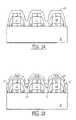
- FIGS. 1A-1Bare cross-sectional views of intermediate structures that illustrated methods of forming integrated circuit devices according to embodiments of the invention.
- FIG. 2Ais a flow diagram of process steps that illustrates methods of forming integrated circuit devices according to embodiments of the present invention.
- FIG. 2Bis a flow diagram of process steps that illustrates methods of forming integrated circuit devices according to additional embodiments of the present invention.
- FIGS. 1A-1Billustrate methods of forming integrated circuit devices according to first embodiments of the present invention.
- a plurality of integrated circuit structuresare formed at side-by-side locations on an integrated circuit substrate 10 .
- These structuresmay include, but are not limited to, structures having relatively narrow aspect ratios (i.e., narrow width-to-height ratios), such as passive electronic devices, interconnects, insulated gate electrodes, etc.
- These insulated gate electrodesare illustrated as including a gate insulating region 12 , an electrically conductive gate electrode 14 and a gate capping layer 16 .
- Electrically insulating sidewall spacers 18are also provided on sidewalls of the gate electrodes 14 , as illustrated.
- FIG. 1Aalso illustrates the formation of an electrically insulating layer 20 as a conformal layer that extends on the integrated circuit structures and in the gaps or spacing between the integrated circuit structures.
- the electrically insulating layer 20may have an undulating surface profile with at least one peak (e.g., on top of each gate electrode) and at least one valley (e.g., in the spaces and gaps between the gate electrodes).
- the electrically insulating layer 20may be a silicon nitride layer. This silicon nitride layer may be formed using a plasma deposition process (e.g., HDP (high density plasma) process).
- HDPhigh density plasma
- This plasma deposition processmay include establishing a first plasma in a plasma processing chamber, using an inert gas (e.g., argon gas), a nitrogen containing gas (e.g., N 2 gas) and a silicon containing gas (e.g., SiH 4 ) as source gases.
- the first plasmamay be established as a relatively low power (e.g., 400 W bias power), high frequency (HF) plasma and the volumetric flow rate of silane (i.e., SiH 4 ) as a source gas may be about 90 sccm.
- the silicon nitride layermay be formed in a deposition chamber using a chemical vapor deposition technique (e.g., PECVD).
- a stepis then performed to selectively thicken portions of the electrically insulating layer 20 by redepositing portions of the electrically insulating layer 20 .
- This redepositingincludes transferring portions of the electrically insulating layer 20 from the peaks to the valleys, to thereby define redeposited insulating regions 22 .
- This transfer of insulating material from the peaks to the valleysmay occur in the plasma processing chamber, with the peaks of the electrically insulating layer 20 acting essentially as sputter targets for charged ions (e.g., nitrogen ions) generated within the plasma processing chamber.
- a second plasmamay be established in the plasma processing chamber using an inert gas (e.g., argon gas) and a nitrogen containing gas (e.g., N 2 gas), but not an appreciable amount of a silicon containing gas, as source gases.
- the second plasmamay be established as a relatively high power (e.g., 1200 W bias power), high frequency (HF) plasma and the volumetric flow rate of the silicon containing source gas may be set to a low level, including about 0 sccm.
- the high level of the plasma bias power associated with the second plasmashould be at least two times greater than the plasma bias power associated with the first plasma.
- FIG. 2Ais a flow diagram of process steps that illustrates additional methods 30 of forming integrated circuit devices, according to embodiments of the present invention.
- a plurality of integrated circuit structurese.g., passive and/or active structures
- At least one electrically insulating layeris then deposited on the integrated circuit substrate.
- This deposition step-may be performed using a chemical vapor deposition technique or a plasma deposition technique, for example. Other deposition techniques may also be used.
- This at least one electrically insulating layerextends on the integrated circuit structures and in the gaps (e.g., spaces) extending between adjacent ones of the integrated circuit structures, Block 34 .
- the resulting electrically insulating layermay have an undulating surface profile with at least one peak (e.g., on top of the integrated circuit structures) and at least one valley (e.g., in the spaces and gaps between the integrated circuit structures).
- the electrically insulating layermay be formed using a dual-stress liner fabrication technique, which may accompany formation of CMOS integrated circuits having closely adjacent NMOS and PMOS transistors.
- the electrically insulating layeris then selectively thickened, Block 36 .
- portions of the electrically insulating layer extending in the gaps between the integrated circuit structuresare thickened by transferring electrically insulating material from the peaks of the electrically insulating layer to the valleys of the electrically insulating layer.
- This material transfer stepis performed by using the peaks of the electrically insulating layer as sputter targets for high energy ions (e.g., N+ ions) established in a high density plasma.
- the use of the peaks of the electrically insulating layer as sputter targetscauses recession of the peaks in the electrically insulating layer and a redeposition of electrically insulating material into the valleys.
- the steps illustrated by Blocks 34 and 36may be repeated to define a sufficiently thick electrically insulating layer. Additional process steps may then be performed to complete an integrated circuit fabrication process at the semiconductor wafer level, Block 40 .
- FIG. 2Bis a flow diagram of process steps that illustrates methods 50 of forming integrated circuit devices, according to embodiments of the present invention.
- a highly integrated array of insulated gate electrodesare formed on a surface of an integrated circuit substrate.
- At least one silicon nitride layeris then deposited on the integrated circuit substrate, Block 34 .
- This deposition stepmay be performed using a chemical vapor deposition technique or a plasma deposition technique, for example. Other deposition techniques may also be used.
- the silicon nitride layeris deposited to extend on the insulated gate electrodes and in the gaps (e.g., spaces) extending between adjacent ones of the insulated gate electrodes.
- the resulting silicon nitride layermay have an undulating surface profile with at least one peak (e.g., on top of the insulated gate electrodes) and at least one valley (e.g., in the spaces and gaps between the insulated gate electrodes).
- the silicon nitride layeris then selectively thickened, Block 56 .
- portions of the silicon nitride layer extending in the gaps between the insulated gate electrodesare thickened by transferring silicon nitride material from the peaks of the silicon nitride layer to the valleys of the silicon nitride layer.
- This material transfer stepis performed by using the peaks of the silicon nitride layer as sputter targets for high energy ions (e.g., N+ ions) established in a high density plasma.
- the use of the peaks of the silicon nitride layer as sputter targetscauses recession of the peaks in the silicon nitride layer and a redeposition of silicon nitride material into the valleys.
- the steps illustrated by Blocks 54 and 56may be repeated to define a sufficiently thick silicon nitride layer. Additional process steps may then be performed to complete an integrated circuit fabrication process at the semiconductor wafer level, Block 60 .
Landscapes
- Engineering & Computer Science (AREA)
- Physics & Mathematics (AREA)
- Power Engineering (AREA)
- Condensed Matter Physics & Semiconductors (AREA)
- General Physics & Mathematics (AREA)
- Manufacturing & Machinery (AREA)
- Computer Hardware Design (AREA)
- Microelectronics & Electronic Packaging (AREA)
- Chemical & Material Sciences (AREA)
- Chemical Kinetics & Catalysis (AREA)
- Plasma & Fusion (AREA)
- General Chemical & Material Sciences (AREA)
- Optics & Photonics (AREA)
- Materials Engineering (AREA)
- Mechanical Engineering (AREA)
- Metallurgy (AREA)
- Organic Chemistry (AREA)
- Formation Of Insulating Films (AREA)
- Internal Circuitry In Semiconductor Integrated Circuit Devices (AREA)
Abstract
Description
- The present invention relates to integrated circuit fabrication methods and, more particularly, to methods of fabricating field effect transistors in integrated circuit substrates.
- Conventional techniques to increase the levels of device integration on integrated circuit substrates can often lead to reductions in device yield and device reliability. Some of these reductions in device yield may be caused by the formation of voids or gaps within electrically insulating layers and also within electrical interconnects that may extend through one or more electrically insulating layers. In particular, the conformal deposition of relatively thick electrically insulating layers on closely-spaced integrated circuit structures having relatively narrow aspect ratios may lead to the formation of voids in the spaces between the integrated circuit structures. These voids can result in the formation of electrical shorts between electrical interconnects and other integrated circuit structures formed on the substrate. One attempt to address this problem includes the use of thinner insulating layers, however, the use of thinner insulating layers may lead to increases in parasitic capacitive coupling between adjacent integrated circuit structures, which can lower device operating speeds. Etch-back and other planarization techniques have also been developed to make the surface profiles of deposited insulating layers more uniform and limit the range of peaks and valleys in the surface profile. Unfortunately, such planarization techniques may not be effective when the layers to be planarized are located very close to a primary surface of an integrated circuit substrate.
- Embodiments of the present invention include methods of forming integrated circuit structures and devices using insulator deposition and insulator gap filling techniques, to thereby define insulating layers having more uniform surface profiles. According to some of these embodiments, methods to form integrated circuit devices include depositing an electrically insulating layer onto an integrated circuit substrate having integrated circuit structures thereon. This deposition step results in the formation of an electrically insulating layer having an undulating surface profile, which includes at least one peak and at least on valley adjacent to the at least one peak. A non-uniform thickening step is then performed. This non-uniform thickening step includes thickening a portion of the electrically insulating layer by redepositing portions of the electrically insulating layer from the least one peak to the at least one valley. This redeposition occurs using a sputter deposition technique that utilizes the electrically insulating layer as a sputter target.
- According to some of these embodiments, the depositing step includes depositing the electrically insulating layer onto the integrated circuit substrate using a plasma deposition process. In particular, the depositing step may include depositing a silicon nitride layer using a first plasma that receives an inert gas (e.g., argon gas), a nitrogen containing gas and a silicon containing gas (e.g., SiH4) as source gases. In addition, the thickening step may include redepositing portions of the silicon nitride layer using a second plasma that receives the inert gas and the nitrogen containing gas, but not the silicon containing gas, as source gases. According to aspects of these embodiments, the plasma bias power used to establish the second plasma is greater than about two times a plasma bias power used to establish the first plasma. The thickening step may also be followed by a step of depositing additional silicon nitride onto the silicon nitride layer using a third plasma equivalent to the first plasma. Another thickening step may then be performed, which follows the step of depositing the additional silicon nitride.
- Additional embodiments of the present invention include methods of forming field effect transistors by forming first and second insulated gate electrodes at side-by-side locations on an integrated circuit substrate and then forming a silicon nitride layer on the first and second insulated gate electrodes and in a gap between the first and second insulated gate electrodes. This step of forming the silicon nitride layer may include depositing the silicon nitride layer using a chemical vapor deposition process (e.g., PECVD) and/or a plasma deposition process. The silicon nitride layer is then selectively thickened. In particular, a portion of the silicon nitride layer located in the gap is then thickened by transferring portions of the silicon nitride layer extending opposite the first and second insulated gate electrodes into the gap using a sputtering process.
- Still further embodiments of the present invention include depositing an electrically insulating layer on an integrated circuit substrate using a first deposition technique and then recessing a first portion of the deposited electrically insulating layer. This recessing step, which may be performed using a plasma redeposition technique having different process conditions relative to the first deposition technique, includes bombarding the first portion of the electrically insulating layer with a sufficient quantity of plasma ions to thereby physically remove electrically insulating material from the first portion of the electrically insulating layer and redeposit the removed electrically insulating material onto a second portion of the electrically insulating layer.
- Additional methods of forming integrated circuit devices include depositing an electrically insulating layer having an undulating surface profile with at least one peak and at least on valley, using a first plasma established in a plasma deposition chamber. The composition of the first plasma is then adjusted by lowering a concentration of at least one source gas supplied thereto (e.g., SiH4), to thereby cause recession of the at least one peak and redepositing of material removed from the at least one peak into the at least one valley. This adjusting step may also be followed by a step of readjusting the composition of the first plasma by increasing the concentration of the at least one source gas supplied thereto, to thereby cause deposition of additional electrically insulating material on the at least one peak.
FIGS. 1A-1B are cross-sectional views of intermediate structures that illustrated methods of forming integrated circuit devices according to embodiments of the invention.FIG. 2A is a flow diagram of process steps that illustrates methods of forming integrated circuit devices according to embodiments of the present invention.FIG. 2B is a flow diagram of process steps that illustrates methods of forming integrated circuit devices according to additional embodiments of the present invention.- The present invention will now be described more fully hereinafter with reference to the accompanying drawings, in which preferred embodiments of the invention are shown. This invention may, however, be embodied in different forms and should not be construed as limited to the embodiments set forth herein. Rather, these embodiments are provided so that this disclosure will be thorough and complete, and will fully convey the scope of the invention to those skilled in the art. In the drawings, the thickness of layers and regions are exaggerated for clarity. It will also be understood that when a layer is referred to as being “on” another layer or substrate, it can be directly on the other layer or substrate, or intervening layers may also be present. Like numbers refer to like elements throughout.
FIGS. 1A-1B illustrate methods of forming integrated circuit devices according to first embodiments of the present invention. As illustrated byFIG. 1A , a plurality of integrated circuit structures are formed at side-by-side locations on anintegrated circuit substrate 10. These structures may include, but are not limited to, structures having relatively narrow aspect ratios (i.e., narrow width-to-height ratios), such as passive electronic devices, interconnects, insulated gate electrodes, etc. These insulated gate electrodes are illustrated as including agate insulating region 12, an electricallyconductive gate electrode 14 and agate capping layer 16. Electrically insulatingsidewall spacers 18 are also provided on sidewalls of thegate electrodes 14, as illustrated.FIG. 1A also illustrates the formation of an electricallyinsulating layer 20 as a conformal layer that extends on the integrated circuit structures and in the gaps or spacing between the integrated circuit structures. As illustrated, the electrically insulatinglayer 20 may have an undulating surface profile with at least one peak (e.g., on top of each gate electrode) and at least one valley (e.g., in the spaces and gaps between the gate electrodes). According to some embodiments of the invention, the electrically insulatinglayer 20 may be a silicon nitride layer. This silicon nitride layer may be formed using a plasma deposition process (e.g., HDP (high density plasma) process). This plasma deposition process may include establishing a first plasma in a plasma processing chamber, using an inert gas (e.g., argon gas), a nitrogen containing gas (e.g., N2gas) and a silicon containing gas (e.g., SiH4) as source gases. The first plasma may be established as a relatively low power (e.g., 400 W bias power), high frequency (HF) plasma and the volumetric flow rate of silane (i.e., SiH4) as a source gas may be about 90 sccm. Alternatively, the silicon nitride layer may be formed in a deposition chamber using a chemical vapor deposition technique (e.g., PECVD).- Referring now to
FIG. 1B , a step is then performed to selectively thicken portions of the electrically insulatinglayer 20 by redepositing portions of the electrically insulatinglayer 20. This redepositing includes transferring portions of the electrically insulatinglayer 20 from the peaks to the valleys, to thereby define redepositedinsulating regions 22. This transfer of insulating material from the peaks to the valleys may occur in the plasma processing chamber, with the peaks of the electrically insulatinglayer 20 acting essentially as sputter targets for charged ions (e.g., nitrogen ions) generated within the plasma processing chamber. These charged ions impact and dislodge the insulating material from the peaks in the electrically insulatinglayer 20 and at least some of this dislodged material redeposit in the valleys of the electrically insulatinglayer 20 to thereby define redeposited insulatingregions 22. The electrically insulatinglayer 20 and the redeposited insulatingregions 22 may then be exposed to a sufficient dose of UV radiation to thereby improve a tensile strength of the insulatingregions 22. - In particular, a second plasma may be established in the plasma processing chamber using an inert gas (e.g., argon gas) and a nitrogen containing gas (e.g., N2gas), but not an appreciable amount of a silicon containing gas, as source gases. The second plasma may be established as a relatively high power (e.g., 1200 W bias power), high frequency (HF) plasma and the volumetric flow rate of the silicon containing source gas may be set to a low level, including about 0 sccm. The high level of the plasma bias power associated with the second plasma should be at least two times greater than the plasma bias power associated with the first plasma.
FIG. 2A is a flow diagram of process steps that illustratesadditional methods 30 of forming integrated circuit devices, according to embodiments of the present invention. As illustrated byBlock 32, a plurality of integrated circuit structures (e.g., passive and/or active structures) are formed on a surface of an integrated circuit substrate. At least one electrically insulating layer is then deposited on the integrated circuit substrate. This deposition step-may be performed using a chemical vapor deposition technique or a plasma deposition technique, for example. Other deposition techniques may also be used. This at least one electrically insulating layer extends on the integrated circuit structures and in the gaps (e.g., spaces) extending between adjacent ones of the integrated circuit structures,Block 34. Based on this deposition step, the resulting electrically insulating layer may have an undulating surface profile with at least one peak (e.g., on top of the integrated circuit structures) and at least one valley (e.g., in the spaces and gaps between the integrated circuit structures). In alternative embodiments of the invention, the electrically insulating layer may be formed using a dual-stress liner fabrication technique, which may accompany formation of CMOS integrated circuits having closely adjacent NMOS and PMOS transistors.- The electrically insulating layer is then selectively thickened,
Block 36. In particular, portions of the electrically insulating layer extending in the gaps between the integrated circuit structures are thickened by transferring electrically insulating material from the peaks of the electrically insulating layer to the valleys of the electrically insulating layer. This material transfer step is performed by using the peaks of the electrically insulating layer as sputter targets for high energy ions (e.g., N+ ions) established in a high density plasma. The use of the peaks of the electrically insulating layer as sputter targets causes recession of the peaks in the electrically insulating layer and a redeposition of electrically insulating material into the valleys. As illustrated by thedecision Block 38, the steps illustrated byBlocks Block 40. FIG. 2B is a flow diagram of process steps that illustratesmethods 50 of forming integrated circuit devices, according to embodiments of the present invention. As illustrated byBlock 52, a highly integrated array of insulated gate electrodes are formed on a surface of an integrated circuit substrate. At least one silicon nitride layer is then deposited on the integrated circuit substrate,Block 34. This deposition step may be performed using a chemical vapor deposition technique or a plasma deposition technique, for example. Other deposition techniques may also be used. The silicon nitride layer is deposited to extend on the insulated gate electrodes and in the gaps (e.g., spaces) extending between adjacent ones of the insulated gate electrodes. Based on this conformal deposition step, the resulting silicon nitride layer may have an undulating surface profile with at least one peak (e.g., on top of the insulated gate electrodes) and at least one valley (e.g., in the spaces and gaps between the insulated gate electrodes).- The silicon nitride layer is then selectively thickened,
Block 56. In particular, portions of the silicon nitride layer extending in the gaps between the insulated gate electrodes are thickened by transferring silicon nitride material from the peaks of the silicon nitride layer to the valleys of the silicon nitride layer. This material transfer step is performed by using the peaks of the silicon nitride layer as sputter targets for high energy ions (e.g., N+ ions) established in a high density plasma. The use of the peaks of the silicon nitride layer as sputter targets causes recession of the peaks in the silicon nitride layer and a redeposition of silicon nitride material into the valleys. As illustrated by thedecision Block 58, the steps illustrated byBlocks Block 60. - In the drawings and specification, there have been disclosed typical preferred embodiments of the invention and, although specific terms are employed, they are used in a generic and descriptive sense only and not for purposes of limitation, the scope of the invention being set forth in the following claims.
Claims (23)
Priority Applications (3)
| Application Number | Priority Date | Filing Date | Title |
|---|---|---|---|
| US11/683,590US7541288B2 (en) | 2007-03-08 | 2007-03-08 | Methods of forming integrated circuit structures using insulator deposition and insulator gap filling techniques |
| SG200801240-3ASG145648A1 (en) | 2007-03-08 | 2008-02-14 | Methods of forming integrated circuit structures using insulator deposition and insulator gap filling techniques |
| KR1020080014484AKR101373733B1 (en) | 2007-03-08 | 2008-02-18 | Method of forming integrated circuit structures using insulator deposition and insulator gap filling techniques |
Applications Claiming Priority (1)
| Application Number | Priority Date | Filing Date | Title |
|---|---|---|---|
| US11/683,590US7541288B2 (en) | 2007-03-08 | 2007-03-08 | Methods of forming integrated circuit structures using insulator deposition and insulator gap filling techniques |
Publications (2)
| Publication Number | Publication Date |
|---|---|
| US20080220584A1true US20080220584A1 (en) | 2008-09-11 |
| US7541288B2 US7541288B2 (en) | 2009-06-02 |
Family
ID=39742076
Family Applications (1)
| Application Number | Title | Priority Date | Filing Date |
|---|---|---|---|
| US11/683,590ActiveUS7541288B2 (en) | 2007-03-08 | 2007-03-08 | Methods of forming integrated circuit structures using insulator deposition and insulator gap filling techniques |
Country Status (3)
| Country | Link |
|---|---|
| US (1) | US7541288B2 (en) |
| KR (1) | KR101373733B1 (en) |
| SG (1) | SG145648A1 (en) |
Cited By (44)
| Publication number | Priority date | Publication date | Assignee | Title |
|---|---|---|---|---|
| WO2010141297A1 (en)* | 2009-06-02 | 2010-12-09 | Hsio Technologies, Llc | Compliant printed circuit wafer level semiconductor package |
| US8525346B2 (en) | 2009-06-02 | 2013-09-03 | Hsio Technologies, Llc | Compliant conductive nano-particle electrical interconnect |
| US8610265B2 (en) | 2009-06-02 | 2013-12-17 | Hsio Technologies, Llc | Compliant core peripheral lead semiconductor test socket |
| US8618649B2 (en) | 2009-06-02 | 2013-12-31 | Hsio Technologies, Llc | Compliant printed circuit semiconductor package |
| US8758067B2 (en) | 2010-06-03 | 2014-06-24 | Hsio Technologies, Llc | Selective metalization of electrical connector or socket housing |
| US8789272B2 (en) | 2009-06-02 | 2014-07-29 | Hsio Technologies, Llc | Method of making a compliant printed circuit peripheral lead semiconductor test socket |
| US8803539B2 (en) | 2009-06-03 | 2014-08-12 | Hsio Technologies, Llc | Compliant wafer level probe assembly |
| US8912812B2 (en) | 2009-06-02 | 2014-12-16 | Hsio Technologies, Llc | Compliant printed circuit wafer probe diagnostic tool |
| US8928344B2 (en) | 2009-06-02 | 2015-01-06 | Hsio Technologies, Llc | Compliant printed circuit socket diagnostic tool |
| US8955215B2 (en) | 2009-05-28 | 2015-02-17 | Hsio Technologies, Llc | High performance surface mount electrical interconnect |
| US8955216B2 (en) | 2009-06-02 | 2015-02-17 | Hsio Technologies, Llc | Method of making a compliant printed circuit peripheral lead semiconductor package |
| US8970031B2 (en) | 2009-06-16 | 2015-03-03 | Hsio Technologies, Llc | Semiconductor die terminal |
| US8981809B2 (en) | 2009-06-29 | 2015-03-17 | Hsio Technologies, Llc | Compliant printed circuit semiconductor tester interface |
| US8981568B2 (en) | 2009-06-16 | 2015-03-17 | Hsio Technologies, Llc | Simulated wirebond semiconductor package |
| US8984748B2 (en) | 2009-06-29 | 2015-03-24 | Hsio Technologies, Llc | Singulated semiconductor device separable electrical interconnect |
| US8987886B2 (en) | 2009-06-02 | 2015-03-24 | Hsio Technologies, Llc | Copper pillar full metal via electrical circuit structure |
| US8988093B2 (en) | 2009-06-02 | 2015-03-24 | Hsio Technologies, Llc | Bumped semiconductor wafer or die level electrical interconnect |
| US9054097B2 (en) | 2009-06-02 | 2015-06-09 | Hsio Technologies, Llc | Compliant printed circuit area array semiconductor device package |
| US9093767B2 (en) | 2009-06-02 | 2015-07-28 | Hsio Technologies, Llc | High performance surface mount electrical interconnect |
| US9184527B2 (en) | 2009-06-02 | 2015-11-10 | Hsio Technologies, Llc | Electrical connector insulator housing |
| US9184145B2 (en) | 2009-06-02 | 2015-11-10 | Hsio Technologies, Llc | Semiconductor device package adapter |
| US9196980B2 (en) | 2009-06-02 | 2015-11-24 | Hsio Technologies, Llc | High performance surface mount electrical interconnect with external biased normal force loading |
| US9232654B2 (en) | 2009-06-02 | 2016-01-05 | Hsio Technologies, Llc | High performance electrical circuit structure |
| US9231328B2 (en) | 2009-06-02 | 2016-01-05 | Hsio Technologies, Llc | Resilient conductive electrical interconnect |
| US9277654B2 (en) | 2009-06-02 | 2016-03-01 | Hsio Technologies, Llc | Composite polymer-metal electrical contacts |
| US9276339B2 (en) | 2009-06-02 | 2016-03-01 | Hsio Technologies, Llc | Electrical interconnect IC device socket |
| US9276336B2 (en) | 2009-05-28 | 2016-03-01 | Hsio Technologies, Llc | Metalized pad to electrical contact interface |
| US9318862B2 (en) | 2009-06-02 | 2016-04-19 | Hsio Technologies, Llc | Method of making an electronic interconnect |
| US9320133B2 (en) | 2009-06-02 | 2016-04-19 | Hsio Technologies, Llc | Electrical interconnect IC device socket |
| US9320144B2 (en) | 2009-06-17 | 2016-04-19 | Hsio Technologies, Llc | Method of forming a semiconductor socket |
| US9350093B2 (en) | 2010-06-03 | 2016-05-24 | Hsio Technologies, Llc | Selective metalization of electrical connector or socket housing |
| US9414500B2 (en) | 2009-06-02 | 2016-08-09 | Hsio Technologies, Llc | Compliant printed flexible circuit |
| US9536815B2 (en) | 2009-05-28 | 2017-01-03 | Hsio Technologies, Llc | Semiconductor socket with direct selective metalization |
| US9559447B2 (en) | 2015-03-18 | 2017-01-31 | Hsio Technologies, Llc | Mechanical contact retention within an electrical connector |
| US9603249B2 (en) | 2009-06-02 | 2017-03-21 | Hsio Technologies, Llc | Direct metalization of electrical circuit structures |
| US9613841B2 (en) | 2009-06-02 | 2017-04-04 | Hsio Technologies, Llc | Area array semiconductor device package interconnect structure with optional package-to-package or flexible circuit to package connection |
| US9689897B2 (en) | 2010-06-03 | 2017-06-27 | Hsio Technologies, Llc | Performance enhanced semiconductor socket |
| US9699906B2 (en) | 2009-06-02 | 2017-07-04 | Hsio Technologies, Llc | Hybrid printed circuit assembly with low density main core and embedded high density circuit regions |
| US9761520B2 (en) | 2012-07-10 | 2017-09-12 | Hsio Technologies, Llc | Method of making an electrical connector having electrodeposited terminals |
| US9930775B2 (en) | 2009-06-02 | 2018-03-27 | Hsio Technologies, Llc | Copper pillar full metal via electrical circuit structure |
| US10159154B2 (en) | 2010-06-03 | 2018-12-18 | Hsio Technologies, Llc | Fusion bonded liquid crystal polymer circuit structure |
| US10506722B2 (en) | 2013-07-11 | 2019-12-10 | Hsio Technologies, Llc | Fusion bonded liquid crystal polymer electrical circuit structure |
| US10667410B2 (en) | 2013-07-11 | 2020-05-26 | Hsio Technologies, Llc | Method of making a fusion bonded circuit structure |
| US20230178633A1 (en)* | 2021-12-08 | 2023-06-08 | Taiwan Semiconductor Manufacturing Company, Ltd. | Self-filling spacer structure |
Families Citing this family (1)
| Publication number | Priority date | Publication date | Assignee | Title |
|---|---|---|---|---|
| US7560723B2 (en)* | 2006-08-29 | 2009-07-14 | Micron Technology, Inc. | Enhanced memory density resistance variable memory cells, arrays, devices and systems including the same, and methods of fabrication |
Citations (20)
| Publication number | Priority date | Publication date | Assignee | Title |
|---|---|---|---|---|
| US4872947A (en)* | 1986-12-19 | 1989-10-10 | Applied Materials, Inc. | CVD of silicon oxide using TEOS decomposition and in-situ planarization process |
| US5000113A (en)* | 1986-12-19 | 1991-03-19 | Applied Materials, Inc. | Thermal CVD/PECVD reactor and use for thermal chemical vapor deposition of silicon dioxide and in-situ multi-step planarized process |
| US5244841A (en)* | 1988-11-10 | 1993-09-14 | Applied Materials, Inc. | Method for planarizing an integrated circuit structure using low melting inorganic material and flowing while depositing |
| US6100205A (en)* | 1997-04-02 | 2000-08-08 | United Microelectronics Corp. | Intermetal dielectric layer formation with low dielectric constant using high density plasma chemical vapor deposition process |
| US6217721B1 (en)* | 1995-08-07 | 2001-04-17 | Applied Materials, Inc. | Filling narrow apertures and forming interconnects with a metal utilizing a crystallographically oriented liner layer |
| US6218284B1 (en)* | 1999-02-01 | 2001-04-17 | United Microelectronics, Corp. | Method for forming an inter-metal dielectric layer |
| US6261891B1 (en)* | 2000-01-28 | 2001-07-17 | United Microelectronics Corp. | Method of forming a passivation layer of a DRAM |
| US6335249B1 (en)* | 2000-02-07 | 2002-01-01 | Taiwan Semiconductor Manufacturing Company | Salicide field effect transistors with improved borderless contact structures and a method of fabrication |
| US6455891B2 (en)* | 2000-04-14 | 2002-09-24 | Sharp Kabushiki Kaisha | Semiconductor device and method for manufacturing the same |
| US20030040158A1 (en)* | 2001-08-21 | 2003-02-27 | Nec Corporation | Semiconductor device and method of fabricating the same |
| US6541370B1 (en)* | 2001-09-17 | 2003-04-01 | Taiwan Semiconductor Manufacturing Co., Ltd. | Composite microelectronic dielectric layer with inhibited crack susceptibility |
| US6664639B2 (en)* | 2000-12-22 | 2003-12-16 | Matrix Semiconductor, Inc. | Contact and via structure and method of fabrication |
| US6787444B2 (en)* | 1993-12-29 | 2004-09-07 | Intel Corporation | Interconnection structures and methods of fabrication |
| US20040175955A1 (en)* | 2002-07-18 | 2004-09-09 | Haselden Barbara A. | Two stage etching of silicon nitride to form a nitride spacer |
| US6858533B2 (en)* | 2002-09-11 | 2005-02-22 | Samsung Electronics Co., Ltd. | Semiconductor device having an etch stopper formed of a sin layer by low temperature ALD and method of fabricating the same |
| US20050269650A1 (en)* | 2004-06-08 | 2005-12-08 | Fujitsu Limited, | Semiconductor device having stress and its manufacture method |
| US20060024879A1 (en)* | 2004-07-31 | 2006-02-02 | Taiwan Semiconductor Manufacturing Co., Ltd. | Selectively strained MOSFETs to improve drive current |
| US7002209B2 (en)* | 2004-05-21 | 2006-02-21 | International Business Machines Corporation | MOSFET structure with high mechanical stress in the channel |
| US7022561B2 (en)* | 2002-12-02 | 2006-04-04 | Taiwan Semiconductor Manufacturing Company, Ltd. | CMOS device |
| US7078346B2 (en)* | 1997-04-02 | 2006-07-18 | United Microelectronics Corporation | High density plasma chemical vapor deposition process |
Family Cites Families (14)
| Publication number | Priority date | Publication date | Assignee | Title |
|---|---|---|---|---|
| JPH0846173A (en) | 1994-07-26 | 1996-02-16 | Mitsubishi Electric Corp | Semiconductor device and manufacturing method thereof |
| KR960015719A (en)* | 1994-10-12 | 1996-05-22 | Method and apparatus for forming a flat layer on a semiconductor substrate using ion bombardment | |
| JPH08250449A (en) | 1995-03-09 | 1996-09-27 | Sony Corp | Formation of connecting hole for semiconductor device |
| JPH09275140A (en) | 1996-04-05 | 1997-10-21 | Sony Corp | Formation of contact hole in semiconductor device |
| JP3593804B2 (en) | 1996-07-24 | 2004-11-24 | ソニー株式会社 | Semiconductor device and manufacturing method thereof |
| KR100293814B1 (en) | 1998-06-26 | 2001-11-05 | 박종섭 | Method of forming etch stopper in thin film transistor |
| KR100319185B1 (en)* | 1998-07-31 | 2002-01-04 | 윤종용 | Method for forming dielectric layer |
| KR20020092682A (en)* | 2001-06-05 | 2002-12-12 | 삼성전자 주식회사 | Method of Forming Dielectric layer in Semiconductor Device |
| JP2003060201A (en) | 2001-08-13 | 2003-02-28 | Hitachi Ltd | Method for manufacturing semiconductor device |
| KR100465601B1 (en) | 2002-07-18 | 2005-01-13 | 주식회사 하이닉스반도체 | A method for forming a semiconductor device |
| KR100546390B1 (en) | 2003-10-24 | 2006-01-26 | 삼성전자주식회사 | Manufacturing method of MOS transistor using dual silicided process |
| KR20050048125A (en) | 2003-11-19 | 2005-05-24 | 매그나칩 반도체 유한회사 | Method of manufacturing semiconductor device |
| KR100557581B1 (en) | 2003-11-28 | 2006-03-03 | 주식회사 하이닉스반도체 | Manufacturing method for semicondutor device |
| KR20050068586A (en) | 2003-12-30 | 2005-07-05 | 매그나칩 반도체 유한회사 | Method of forming a nitride layer for borderless contact in a semiconductor device |
- 2007
- 2007-03-08USUS11/683,590patent/US7541288B2/enactiveActive
- 2008
- 2008-02-14SGSG200801240-3Apatent/SG145648A1/enunknown
- 2008-02-18KRKR1020080014484Apatent/KR101373733B1/enactiveActive
Patent Citations (20)
| Publication number | Priority date | Publication date | Assignee | Title |
|---|---|---|---|---|
| US4872947A (en)* | 1986-12-19 | 1989-10-10 | Applied Materials, Inc. | CVD of silicon oxide using TEOS decomposition and in-situ planarization process |
| US5000113A (en)* | 1986-12-19 | 1991-03-19 | Applied Materials, Inc. | Thermal CVD/PECVD reactor and use for thermal chemical vapor deposition of silicon dioxide and in-situ multi-step planarized process |
| US5244841A (en)* | 1988-11-10 | 1993-09-14 | Applied Materials, Inc. | Method for planarizing an integrated circuit structure using low melting inorganic material and flowing while depositing |
| US6787444B2 (en)* | 1993-12-29 | 2004-09-07 | Intel Corporation | Interconnection structures and methods of fabrication |
| US6217721B1 (en)* | 1995-08-07 | 2001-04-17 | Applied Materials, Inc. | Filling narrow apertures and forming interconnects with a metal utilizing a crystallographically oriented liner layer |
| US6100205A (en)* | 1997-04-02 | 2000-08-08 | United Microelectronics Corp. | Intermetal dielectric layer formation with low dielectric constant using high density plasma chemical vapor deposition process |
| US7078346B2 (en)* | 1997-04-02 | 2006-07-18 | United Microelectronics Corporation | High density plasma chemical vapor deposition process |
| US6218284B1 (en)* | 1999-02-01 | 2001-04-17 | United Microelectronics, Corp. | Method for forming an inter-metal dielectric layer |
| US6261891B1 (en)* | 2000-01-28 | 2001-07-17 | United Microelectronics Corp. | Method of forming a passivation layer of a DRAM |
| US6335249B1 (en)* | 2000-02-07 | 2002-01-01 | Taiwan Semiconductor Manufacturing Company | Salicide field effect transistors with improved borderless contact structures and a method of fabrication |
| US6455891B2 (en)* | 2000-04-14 | 2002-09-24 | Sharp Kabushiki Kaisha | Semiconductor device and method for manufacturing the same |
| US6664639B2 (en)* | 2000-12-22 | 2003-12-16 | Matrix Semiconductor, Inc. | Contact and via structure and method of fabrication |
| US20030040158A1 (en)* | 2001-08-21 | 2003-02-27 | Nec Corporation | Semiconductor device and method of fabricating the same |
| US6541370B1 (en)* | 2001-09-17 | 2003-04-01 | Taiwan Semiconductor Manufacturing Co., Ltd. | Composite microelectronic dielectric layer with inhibited crack susceptibility |
| US20040175955A1 (en)* | 2002-07-18 | 2004-09-09 | Haselden Barbara A. | Two stage etching of silicon nitride to form a nitride spacer |
| US6858533B2 (en)* | 2002-09-11 | 2005-02-22 | Samsung Electronics Co., Ltd. | Semiconductor device having an etch stopper formed of a sin layer by low temperature ALD and method of fabricating the same |
| US7022561B2 (en)* | 2002-12-02 | 2006-04-04 | Taiwan Semiconductor Manufacturing Company, Ltd. | CMOS device |
| US7002209B2 (en)* | 2004-05-21 | 2006-02-21 | International Business Machines Corporation | MOSFET structure with high mechanical stress in the channel |
| US20050269650A1 (en)* | 2004-06-08 | 2005-12-08 | Fujitsu Limited, | Semiconductor device having stress and its manufacture method |
| US20060024879A1 (en)* | 2004-07-31 | 2006-02-02 | Taiwan Semiconductor Manufacturing Co., Ltd. | Selectively strained MOSFETs to improve drive current |
Cited By (54)
| Publication number | Priority date | Publication date | Assignee | Title |
|---|---|---|---|---|
| US8955215B2 (en) | 2009-05-28 | 2015-02-17 | Hsio Technologies, Llc | High performance surface mount electrical interconnect |
| US9660368B2 (en) | 2009-05-28 | 2017-05-23 | Hsio Technologies, Llc | High performance surface mount electrical interconnect |
| US9536815B2 (en) | 2009-05-28 | 2017-01-03 | Hsio Technologies, Llc | Semiconductor socket with direct selective metalization |
| US9276336B2 (en) | 2009-05-28 | 2016-03-01 | Hsio Technologies, Llc | Metalized pad to electrical contact interface |
| US9613841B2 (en) | 2009-06-02 | 2017-04-04 | Hsio Technologies, Llc | Area array semiconductor device package interconnect structure with optional package-to-package or flexible circuit to package connection |
| US9930775B2 (en) | 2009-06-02 | 2018-03-27 | Hsio Technologies, Llc | Copper pillar full metal via electrical circuit structure |
| US8789272B2 (en) | 2009-06-02 | 2014-07-29 | Hsio Technologies, Llc | Method of making a compliant printed circuit peripheral lead semiconductor test socket |
| US10609819B2 (en) | 2009-06-02 | 2020-03-31 | Hsio Technologies, Llc | Hybrid printed circuit assembly with low density main core and embedded high density circuit regions |
| US8829671B2 (en) | 2009-06-02 | 2014-09-09 | Hsio Technologies, Llc | Compliant core peripheral lead semiconductor socket |
| US8912812B2 (en) | 2009-06-02 | 2014-12-16 | Hsio Technologies, Llc | Compliant printed circuit wafer probe diagnostic tool |
| US8928344B2 (en) | 2009-06-02 | 2015-01-06 | Hsio Technologies, Llc | Compliant printed circuit socket diagnostic tool |
| US8704377B2 (en) | 2009-06-02 | 2014-04-22 | Hsio Technologies, Llc | Compliant conductive nano-particle electrical interconnect |
| US8955216B2 (en) | 2009-06-02 | 2015-02-17 | Hsio Technologies, Llc | Method of making a compliant printed circuit peripheral lead semiconductor package |
| US9276339B2 (en) | 2009-06-02 | 2016-03-01 | Hsio Technologies, Llc | Electrical interconnect IC device socket |
| US9699906B2 (en) | 2009-06-02 | 2017-07-04 | Hsio Technologies, Llc | Hybrid printed circuit assembly with low density main core and embedded high density circuit regions |
| US8525346B2 (en) | 2009-06-02 | 2013-09-03 | Hsio Technologies, Llc | Compliant conductive nano-particle electrical interconnect |
| WO2010141297A1 (en)* | 2009-06-02 | 2010-12-09 | Hsio Technologies, Llc | Compliant printed circuit wafer level semiconductor package |
| US8987886B2 (en) | 2009-06-02 | 2015-03-24 | Hsio Technologies, Llc | Copper pillar full metal via electrical circuit structure |
| US8988093B2 (en) | 2009-06-02 | 2015-03-24 | Hsio Technologies, Llc | Bumped semiconductor wafer or die level electrical interconnect |
| US9054097B2 (en) | 2009-06-02 | 2015-06-09 | Hsio Technologies, Llc | Compliant printed circuit area array semiconductor device package |
| US9076884B2 (en) | 2009-06-02 | 2015-07-07 | Hsio Technologies, Llc | Compliant printed circuit semiconductor package |
| US9093767B2 (en) | 2009-06-02 | 2015-07-28 | Hsio Technologies, Llc | High performance surface mount electrical interconnect |
| US9136196B2 (en) | 2009-06-02 | 2015-09-15 | Hsio Technologies, Llc | Compliant printed circuit wafer level semiconductor package |
| US9184527B2 (en) | 2009-06-02 | 2015-11-10 | Hsio Technologies, Llc | Electrical connector insulator housing |
| US9184145B2 (en) | 2009-06-02 | 2015-11-10 | Hsio Technologies, Llc | Semiconductor device package adapter |
| US9196980B2 (en) | 2009-06-02 | 2015-11-24 | Hsio Technologies, Llc | High performance surface mount electrical interconnect with external biased normal force loading |
| US9232654B2 (en) | 2009-06-02 | 2016-01-05 | Hsio Technologies, Llc | High performance electrical circuit structure |
| US9231328B2 (en) | 2009-06-02 | 2016-01-05 | Hsio Technologies, Llc | Resilient conductive electrical interconnect |
| US9603249B2 (en) | 2009-06-02 | 2017-03-21 | Hsio Technologies, Llc | Direct metalization of electrical circuit structures |
| US9277654B2 (en) | 2009-06-02 | 2016-03-01 | Hsio Technologies, Llc | Composite polymer-metal electrical contacts |
| US8618649B2 (en) | 2009-06-02 | 2013-12-31 | Hsio Technologies, Llc | Compliant printed circuit semiconductor package |
| US9318862B2 (en) | 2009-06-02 | 2016-04-19 | Hsio Technologies, Llc | Method of making an electronic interconnect |
| US9320133B2 (en) | 2009-06-02 | 2016-04-19 | Hsio Technologies, Llc | Electrical interconnect IC device socket |
| US8610265B2 (en) | 2009-06-02 | 2013-12-17 | Hsio Technologies, Llc | Compliant core peripheral lead semiconductor test socket |
| US9414500B2 (en) | 2009-06-02 | 2016-08-09 | Hsio Technologies, Llc | Compliant printed flexible circuit |
| US8803539B2 (en) | 2009-06-03 | 2014-08-12 | Hsio Technologies, Llc | Compliant wafer level probe assembly |
| US8981568B2 (en) | 2009-06-16 | 2015-03-17 | Hsio Technologies, Llc | Simulated wirebond semiconductor package |
| US8970031B2 (en) | 2009-06-16 | 2015-03-03 | Hsio Technologies, Llc | Semiconductor die terminal |
| US9320144B2 (en) | 2009-06-17 | 2016-04-19 | Hsio Technologies, Llc | Method of forming a semiconductor socket |
| US8981809B2 (en) | 2009-06-29 | 2015-03-17 | Hsio Technologies, Llc | Compliant printed circuit semiconductor tester interface |
| US8984748B2 (en) | 2009-06-29 | 2015-03-24 | Hsio Technologies, Llc | Singulated semiconductor device separable electrical interconnect |
| US9350093B2 (en) | 2010-06-03 | 2016-05-24 | Hsio Technologies, Llc | Selective metalization of electrical connector or socket housing |
| US8758067B2 (en) | 2010-06-03 | 2014-06-24 | Hsio Technologies, Llc | Selective metalization of electrical connector or socket housing |
| US9689897B2 (en) | 2010-06-03 | 2017-06-27 | Hsio Technologies, Llc | Performance enhanced semiconductor socket |
| US10159154B2 (en) | 2010-06-03 | 2018-12-18 | Hsio Technologies, Llc | Fusion bonded liquid crystal polymer circuit structure |
| US9350124B2 (en) | 2010-12-01 | 2016-05-24 | Hsio Technologies, Llc | High speed circuit assembly with integral terminal and mating bias loading electrical connector assembly |
| US9761520B2 (en) | 2012-07-10 | 2017-09-12 | Hsio Technologies, Llc | Method of making an electrical connector having electrodeposited terminals |
| US10453789B2 (en) | 2012-07-10 | 2019-10-22 | Hsio Technologies, Llc | Electrodeposited contact terminal for use as an electrical connector or semiconductor packaging substrate |
| US10506722B2 (en) | 2013-07-11 | 2019-12-10 | Hsio Technologies, Llc | Fusion bonded liquid crystal polymer electrical circuit structure |
| US10667410B2 (en) | 2013-07-11 | 2020-05-26 | Hsio Technologies, Llc | Method of making a fusion bonded circuit structure |
| US9559447B2 (en) | 2015-03-18 | 2017-01-31 | Hsio Technologies, Llc | Mechanical contact retention within an electrical connector |
| US9755335B2 (en) | 2015-03-18 | 2017-09-05 | Hsio Technologies, Llc | Low profile electrical interconnect with fusion bonded contact retention and solder wick reduction |
| US20230178633A1 (en)* | 2021-12-08 | 2023-06-08 | Taiwan Semiconductor Manufacturing Company, Ltd. | Self-filling spacer structure |
| DE102022104004A1 (en) | 2021-12-08 | 2023-06-15 | Taiwan Semiconductor Manufacturing Co., Ltd. | SELF-FILLING SPACER STRUCTURE |
Also Published As
| Publication number | Publication date |
|---|---|
| KR20080082443A (en) | 2008-09-11 |
| US7541288B2 (en) | 2009-06-02 |
| KR101373733B1 (en) | 2014-03-14 |
| SG145648A1 (en) | 2008-09-29 |
Similar Documents
| Publication | Publication Date | Title |
|---|---|---|
| US7541288B2 (en) | Methods of forming integrated circuit structures using insulator deposition and insulator gap filling techniques | |
| US6087278A (en) | Method for fabricating semiconductor devices having an HDP-CVD oxide layer as a passivation layer | |
| US7851376B2 (en) | Compressive nitride film and method of manufacturing thereof | |
| KR100462097B1 (en) | A method of forming a titanium nitride film and the product prepared by said method | |
| US20020052119A1 (en) | In-situ flowing bpsg gap fill process using hdp | |
| US7741671B2 (en) | Capacitor for a semiconductor device and manufacturing method thereof | |
| JP3492634B2 (en) | Method for filling a gap on a semiconductor wafer | |
| US9496327B2 (en) | High precision capacitor dielectric | |
| US7247252B2 (en) | Method of avoiding plasma arcing during RIE etching | |
| US20070238254A1 (en) | Method of etching low dielectric constant films | |
| US7442638B2 (en) | Method for forming a tungsten interconnect structure with enhanced sidewall coverage of the barrier layer | |
| CN101207067A (en) | Method for manufacturing inlaid structure | |
| KR20040059842A (en) | Method for forming a contact hole in a semiconductor device | |
| US20090102053A1 (en) | Metal line stacking structure in semiconductor device and formation method thereof | |
| JP3601988B2 (en) | Method of forming insulating film | |
| US20070152241A1 (en) | Gate Capacitor Having Horizontal Structure and Method for Manufacturing the Same | |
| KR100529388B1 (en) | Method of forming intermediate insulating layer for semiconductor device | |
| KR100505629B1 (en) | Method for filling a trench | |
| JPH09129625A (en) | Formation of interlayer insulating film of semiconductor element | |
| JP2001035845A (en) | Manufacturing method of semiconductor device and plasma insulating film forming device which is used for that | |
| KR100641501B1 (en) | Metal line formation method of semiconductor device | |
| US20060138667A1 (en) | Method for forming an intermetal dielectric layer in a semiconductor device using HDP-CVD, and a semiconductor device manufactured thereby | |
| KR100533880B1 (en) | High Density Plasma Chemical Vapor Deposition Method | |
| JP2001102455A (en) | Method for forming a contact-point opening in dielectrics layer of semiconductor device | |
| KR20030058015A (en) | Method of forming high density plasm oxide layer for semiconductor device |
Legal Events
| Date | Code | Title | Description |
|---|---|---|---|
| AS | Assignment | Owner name:SAMSUNG ELECTRONICS CO., LTD., KOREA, REPUBLIC OF Free format text:ASSIGNMENT OF ASSIGNORS INTEREST;ASSIGNORS:KIM, JUN JUNG;KU, JA HUM;PARK, JAE EON;REEL/FRAME:018981/0376;SIGNING DATES FROM 20061111 TO 20061128 | |
| AS | Assignment | Owner name:INFINEON TECHNOLOGIES NORTH AMERICA CORP., CALIFOR Free format text:ASSIGNMENT OF ASSIGNORS INTEREST;ASSIGNORS:GUTMANN, ALOIS;KWON, O SUNG;REEL/FRAME:019158/0639 Effective date:20070326 | |
| AS | Assignment | Owner name:INFINEON TECHNOLOGIES AG, GERMANY Free format text:ASSIGNMENT OF ASSIGNORS INTEREST;ASSIGNOR:INFINEON TECHNOLOGIES NORTH AMERICA CORP.;REEL/FRAME:019168/0507 Effective date:20070416 Owner name:INFINEON TECHNOLOGIES AG,GERMANY Free format text:ASSIGNMENT OF ASSIGNORS INTEREST;ASSIGNOR:INFINEON TECHNOLOGIES NORTH AMERICA CORP.;REEL/FRAME:019168/0507 Effective date:20070416 | |
| AS | Assignment | Owner name:INTERNATIONAL BUSINESS MACHINES CORPORATION, NEW Y Free format text:ASSIGNMENT OF ASSIGNORS INTEREST;ASSIGNORS:FANG, SUNFEI;YANG, DAE WON;REEL/FRAME:019418/0810 Effective date:20070521 Owner name:CHARTERED SEMICONDUCTOR MANUFACTURING LTD., SINGAP Free format text:ASSIGNMENT OF ASSIGNORS INTEREST;ASSIGNOR:WIDODO, JOHNNY;REEL/FRAME:019418/0785 Effective date:20070517 | |
| FEPP | Fee payment procedure | Free format text:PAYOR NUMBER ASSIGNED (ORIGINAL EVENT CODE: ASPN); ENTITY STATUS OF PATENT OWNER: LARGE ENTITY | |
| STCF | Information on status: patent grant | Free format text:PATENTED CASE | |
| FPAY | Fee payment | Year of fee payment:4 | |
| AS | Assignment | Owner name:GLOBALFOUNDRIES U.S. 2 LLC, NEW YORK Free format text:ASSIGNMENT OF ASSIGNORS INTEREST;ASSIGNOR:INTERNATIONAL BUSINESS MACHINES CORPORATION;REEL/FRAME:036550/0001 Effective date:20150629 | |
| AS | Assignment | Owner name:GLOBALFOUNDRIES INC., CAYMAN ISLANDS Free format text:ASSIGNMENT OF ASSIGNORS INTEREST;ASSIGNORS:GLOBALFOUNDRIES U.S. 2 LLC;GLOBALFOUNDRIES U.S. INC.;REEL/FRAME:036779/0001 Effective date:20150910 | |
| FPAY | Fee payment | Year of fee payment:8 | |
| AS | Assignment | Owner name:WILMINGTON TRUST, NATIONAL ASSOCIATION, DELAWARE Free format text:SECURITY AGREEMENT;ASSIGNOR:GLOBALFOUNDRIES INC.;REEL/FRAME:049490/0001 Effective date:20181127 | |
| MAFP | Maintenance fee payment | Free format text:PAYMENT OF MAINTENANCE FEE, 12TH YEAR, LARGE ENTITY (ORIGINAL EVENT CODE: M1553); ENTITY STATUS OF PATENT OWNER: LARGE ENTITY Year of fee payment:12 | |
| AS | Assignment | Owner name:CHARTERED SEMICONDUCTOR MANUFACTURING PTE. LTD., SINGAPORE Free format text:CHANGE OF NAME;ASSIGNOR:CHARTERED SEMICONDUCTOR MANUFACTURING LTD.;REEL/FRAME:054452/0378 Effective date:20100122 | |
| AS | Assignment | Owner name:GLOBALFOUNDRIES SINGAPORE PTE. LTD., SINGAPORE Free format text:CHANGE OF NAME;ASSIGNOR:CHARTERED SEMICONDUCTOR MANUFACTURING PTE. LTD.;REEL/FRAME:054476/0121 Effective date:20100122 | |
| AS | Assignment | Owner name:GLOBALFOUNDRIES INC., CAYMAN ISLANDS Free format text:RELEASE BY SECURED PARTY;ASSIGNOR:WILMINGTON TRUST, NATIONAL ASSOCIATION;REEL/FRAME:054482/0424 Effective date:20200410 Owner name:TAIWAN SEMICONDUCTOR MANUFACTURING CO., LTD., TAIWAN Free format text:ASSIGNMENT OF ASSIGNORS INTEREST;ASSIGNORS:GLOBALFOUNDRIES INC.;GLOBALFOUNDRIES SINGAPORE PTE. LTD.;REEL/FRAME:054482/0767 Effective date:20200515 | |
| AS | Assignment | Owner name:GLOBALFOUNDRIES INC., CAYMAN ISLANDS Free format text:RELEASE BY SECURED PARTY;ASSIGNOR:WILMINGTON TRUST, NATIONAL ASSOCIATION;REEL/FRAME:054636/0001 Effective date:20201117 |