US20080218615A1 - Apparatus and method for stabilizing image sensor black level - Google Patents
Apparatus and method for stabilizing image sensor black levelDownload PDFInfo
- Publication number
- US20080218615A1 US20080218615A1US11/715,808US71580807AUS2008218615A1US 20080218615 A1US20080218615 A1US 20080218615A1US 71580807 AUS71580807 AUS 71580807AUS 2008218615 A1US2008218615 A1US 2008218615A1
- Authority
- US
- United States
- Prior art keywords
- black
- output signal
- noise
- column
- line
- Prior art date
- Legal status (The legal status is an assumption and is not a legal conclusion. Google has not performed a legal analysis and makes no representation as to the accuracy of the status listed.)
- Granted
Links
Images


Classifications
- H—ELECTRICITY
- H04—ELECTRIC COMMUNICATION TECHNIQUE
- H04N—PICTORIAL COMMUNICATION, e.g. TELEVISION
- H04N25/00—Circuitry of solid-state image sensors [SSIS]; Control thereof
- H04N25/60—Noise processing, e.g. detecting, correcting, reducing or removing noise
- H04N25/618—Noise processing, e.g. detecting, correcting, reducing or removing noise for random or high-frequency noise
- H—ELECTRICITY
- H04—ELECTRIC COMMUNICATION TECHNIQUE
- H04N—PICTORIAL COMMUNICATION, e.g. TELEVISION
- H04N25/00—Circuitry of solid-state image sensors [SSIS]; Control thereof
- H04N25/60—Noise processing, e.g. detecting, correcting, reducing or removing noise
- H04N25/63—Noise processing, e.g. detecting, correcting, reducing or removing noise applied to dark current
- H04N25/633—Noise processing, e.g. detecting, correcting, reducing or removing noise applied to dark current by using optical black pixels
- H—ELECTRICITY
- H04—ELECTRIC COMMUNICATION TECHNIQUE
- H04N—PICTORIAL COMMUNICATION, e.g. TELEVISION
- H04N25/00—Circuitry of solid-state image sensors [SSIS]; Control thereof
- H04N25/60—Noise processing, e.g. detecting, correcting, reducing or removing noise
- H04N25/67—Noise processing, e.g. detecting, correcting, reducing or removing noise applied to fixed-pattern noise, e.g. non-uniformity of response
- H04N25/671—Noise processing, e.g. detecting, correcting, reducing or removing noise applied to fixed-pattern noise, e.g. non-uniformity of response for non-uniformity detection or correction
- H04N25/673—Noise processing, e.g. detecting, correcting, reducing or removing noise applied to fixed-pattern noise, e.g. non-uniformity of response for non-uniformity detection or correction by using reference sources
- H—ELECTRICITY
- H04—ELECTRIC COMMUNICATION TECHNIQUE
- H04N—PICTORIAL COMMUNICATION, e.g. TELEVISION
- H04N25/00—Circuitry of solid-state image sensors [SSIS]; Control thereof
- H04N25/60—Noise processing, e.g. detecting, correcting, reducing or removing noise
- H04N25/67—Noise processing, e.g. detecting, correcting, reducing or removing noise applied to fixed-pattern noise, e.g. non-uniformity of response
- H04N25/671—Noise processing, e.g. detecting, correcting, reducing or removing noise applied to fixed-pattern noise, e.g. non-uniformity of response for non-uniformity detection or correction
- H04N25/677—Noise processing, e.g. detecting, correcting, reducing or removing noise applied to fixed-pattern noise, e.g. non-uniformity of response for non-uniformity detection or correction for reducing the column or line fixed pattern noise
Definitions
- the present inventionis related to: U.S. patent application Ser. No. TBD, entitled, “CROSS-COUPLED DIFFERENTIAL DAC-BASED CLAMP CIRCUIT,” filed TBD; U.S. patent application Ser. No. TBD, entitled, “ON-CHIP BLACK CLAMPING CIRCUIT FOR CMOS IMAGE SENSOR,” filed TBD; and U.S. patent application Ser. No. TBD, entitled, “METHOD FOR BLACK CLAMP CORRECTION INDEPENDENT OF GAIN,” filed TBD; the disclosures of which are herein incorporated by reference.
- the present inventionrelates generally to electronic imaging sensors and, specifically, to advanced imaging system-on-chip (iSoC) sensors having embedded signal processing functions.
- iSoCadvanced imaging system-on-chip
- Imaging sensorsoperate by collecting light intensity in a contiguous array of imaging pixels. Each pixel will have a charge proportional to the intensity of the light incident on the pixel over the duration of exposure. This charge is a “pixel value” that must be read out with as little noise as possible to capture a high quality image or generate video.
- modem CMOS sensorshave lower temporal noise than CCD imaging sensors at data rate >25 MHz, several sources of systematic artifacts can degrade image quality, especially at low illumination.
- Readout of the image electronically reproduced in CMOS imaging sensorsis achieved by routing the signal from each row of pixels through a set of column buffers to the output as shown in FIG. 1 from U.S. Pat. No. 6,861,634.
- Each column buffer 102normally supports a specific column of pixels and is constructed using an integrated amplifier block such as taught in U.S. Pat. No. 5,892,540.
- U.S. Pat. No. 5,172,249subtracts amplifier offsets and FPN by applying signal and reference levels to the input of a subtraction circuit, such as a differential amplifier, without due consideration for the deleterious impact of wideband noise in causing offset correction errors.
- U.S. Pat. No. 6,037,577alternatively provides means to suppress row noise on a row-by-row basis.
- the primary intentis again to suppress offsets from switching noise and charge redistribution among the parallel signal paths rather than to eliminate discretely sampled common reference noise.
- U.S. Pat. No. 6,861,634subsequently teaches a technique for subtracting reference noise in addition to other sources of sensor noise.
- the noise subtractionis performed in the analog domain using a correction value previously determined in the digital domain.
- the analog valueis supplied to a sample-and-hold circuit including a charge amplifier for subtracting the offset.
- the preferred embodimentteaches pseudo-differential or differential signal paths using the pixel's signal level and associated reset level. Unfortunately, burdening the signal path by also supplying the reset level to the offset-subtracting amplifier halves the maximum video rate, doubles the concomitant video bandwidth, and boosts white noise.
- the correctionis also carried out at high speed on a pixel-by-pixel and per-color basis, thus increasing complexity and signal processing overhead.
- the present inventionincludes a method, circuit implementation and firmware code that together provide superior black level stabilization.
- Analog circuits, digital circuits, and algorithmsjointly suppress the various fixed pattern noise sources inherent in “reading out” arrays of image-sensing pixels, while simultaneously maximizing the dynamic range in the analog domain.
- the noise suppressionis performed in the digital domain using algorithms specifically optimized to produce electronic images with useful image quality spanning at least 16 bits of dynamic range, even though only 12 bits may be supplied to the camera from frame-to-frame.
- the present inventioncomprises an apparatus for processing a signal output from a pixel array, the pixel array having optical black pixels and active clear pixels, the apparatus comprising a black clamp block, wherein the black clamp block receives an output signal from the pixel array, compares a black level from the output signal to a black reference value, and outputs an adjustment signal based on the comparison to adjust a black level in the output signal;
- a line noise correction blockreceives the output signal adjusted by the black clamp block, calculates a line noise average value for black pixels in the output signal on a line-by-line basis, calculates a line noise offset based on a difference between the line noise average and the black reference value, and applies the line noise offset to clear pixels in the output signal;
- a column noise correction blockcalculates a column noise offset for black pixels in the output signal, and applies the column noise offset to the clear pixels in the output signal;
- the column noise offsetis calculated on a column basis by comparing the output signal for each black pixel with the line noise average value calculated by the line noise correction block.
- the apparatusmay further comprise a column noise correction memory, the memory storing column noise offset coefficients, wherein the column noise offset coefficients are updated using a differential technique, such that coefficients stored in the memory represent a difference of column noise relative to line noise.
- Another embodiment of the present inventioncomprises a signal processing circuit for processing an output signal from a pixel array, the pixel array having optical black pixels and active clear pixels, the circuit comprising a differential programmable gain amplifier, one input of the differential programmable gain amplifier connected to the output signal from the pixel array;
- an analog-to-digital converterconnected to the differential programmable gain amplifier, wherein the analog-to-digital converter converts an output signal from the programmable gain amplifier into a digitized output signal
- a black clamp processing blockconnected to the analog-to-digital converter, wherein the black clamp processing block compares the digitized output signal with a black reference value, and outputs a black level adjustment signal to an input of the programmable gain amplifier;
- a line noise correction processing blockconnected to the analog-to-digital converter, wherein the line noise correction processing block calculates a line noise average value for black pixels in the output signal on a line-by-line basis, and calculates a line noise offset based on a difference between the line noise average value and the black reference value;
- the column noise correction processing blockcalculates a column noise offset for black pixels in the digitized output signal, the column noise offset calculated on a column basis by comparing the digitized output signal for each black pixel with the line noise average value calculated by the line noise correction processing block;
- a second adderto add the line noise offset to the clear pixels in the digitized output signal.
- the circuit of the present inventionmay further comprise a column noise correction memory, the memory storing column noise offset coefficients, wherein column noise offset coefficients are updated using a differential technique, such that coefficients stored in the memory represent a difference of column noise relative to line noise.
- a method of the present inventionincludes a method to process an output signal from a pixel array, the pixel array having optical black pixels and active clear pixels, the method comprising:
- calculating a black level adjustment signalcomprises:
- calculating a line noise correction valuecomprises:
- the methodmay further includes storing column noise offset coefficients in a memory and updating them using a differential technique, such that the coefficients stored in the memory represent a difference of column noise relative to line noise.
- FIG. 1is a block diagram of a prior art CMOS APS system with digital correction terms applied via analog circuits from U.S. Pat. No. 6,861,634;
- FIG. 3is a block diagram of a prior art architecture for processing output from an image sensor
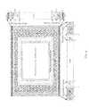
- FIG. 4is a block diagram showing a representative embodiment of a sensor array including active pixels, black reference or optically black (OB) pixels, dummy pixels and guard bands;
- OBoptically black
- FIG. 6is a block diagram of an embodiment of the present invention integrated in a typical imaging System-on-Chip sensor
- FIG. 7is a diagram of the imaging System on Chip data stream that specifically shows the output of the black reference pixels and the time intervals for updating the sensor's black reference level;
- FIG. 8is a block diagram of the pixel array of the present invention including the black pixel regions and active clear pixel regions;
- FIG. 9is a schematic diagram of a preferred embodiment of the present invention including support for black-clamping, line noise suppression and column noise suppression;
- FIG. 10is a schematic diagram of an embodiment of the present invention incorporating a digitally-controlled charge pump as analog black clamping circuit
- FIG. 11is a schematic diagram of a preferred embodiment of the present invention incorporating programmable DAC as analog black clamping means disclosed in related U.S. patent application Ser. No. TBD, entitled, CROSS-COUPLED DIFFERENTIAL DAC-BASED CLAMP CIRCUIT;
- FIG. 12is a schematic diagram of an embodiment of the present invention including support for two data channels
- FIG. 13Abegins a listing of an implementation of the Verilog code for general black clamping in BlackClamp Block 500 ;
- FIG. 13Bcontinues the code of FIG. 13A ;
- FIG. 13Ccontinues the code of FIG. 13B ;
- FIG. 13Dcontinues the code of FIG. 13C ;
- FIG. 13Econtinues the code of FIG. 13D ;
- FIG. 13Fcompletes the Verilog code for implementing BlackClamp Block 500 listed in FIGS. 13A through 13E ;
- FIG. 14lists the programming registers pertaining to line noise suppression
- FIG. 16illustrates the effect of column noise correction as it is applied to a row (line) of pixels.
- the present inventionincludes a representative design for an active-pixel CMOS imager.
- a prototype embodiment of the low-noise active pixel sensor (APS) inventioncan be constructed, for example, as a visible imager comprising an active array of 4096 (columns) by 3072 (rows) of visible light detectors (photodetectors).
- the active array, or nominal record areais bounded by black reference pixels in the surrounding periphery.
- FIG. 4is an array plan showing a nominal record area enclosed by a perimeter of optical black (OB), guard band, dummy, and optional optical alignment pixels.
- OBoptical black
- the rows and columns of pixelscan be spaced 4 microns center-to-center using 0.18 ⁇ m design rules to provide as-drawn optical fill factor of ⁇ 50% for each pixel without microlens.
- Several columns and rows of detectors at the perimeter of the light-sensitive regionare normally covered with metal and/or other opaque material layers to form the OB pixels. Constantly reading the OB pixels during the various blanking intervals, i.e., time segments during which photo-generated data is not supplied by the sensor, enables the present invention to update and stabilize the black level.
- the black level stabilization of the present inventionincludes three types to maximize sensor performance over wide range in sensor temperature and environment.
- the stabilization modesinclude: 1) general black-level clamping; 2) fine-tuning of black level on a line-by-line basis to compensate line noise with appropriate line-based coefficients, and; 3) fine-tuning of black level on a column-by-column basis to adjust for column noise.
- the light-sensitive detectors in each rowcan be covered with color filters to produce color imagers.
- the odd rowsmay begin at the left with red, green, then blue filters, and the even rows may begin with blue, red, then green filters, with these patterns repeating to fill the respective rows.
- a standard Bayer filter patterncan also be applied.
- the video signal from the active pixel sensorhence includes:
- all black pixelscan be read during the “front porch” of the aggregate data stream including data from the black and active pixels of each line of the imaging sensor.
- the active pixelsare often read during a continuous interval preceded by a “front porch” and followed by a “back porch” as defined by various timing standards such as, e.g., SMPTE 274M or SMPTE 292 specifications for high definition video, herein incorporated by reference.
- the term “porch”refers to an interval during each video line, field or frame, wherein actual imaging data is not being supplied to the camera and overhead signal processing functions can instead be performed. Such blanking intervals were originally required for CRT displays for beam flyback.
- the relevant OB pixel datacan all be read during the front porch, split between front porch and black porch, or altogether read during the back porch. While the OB data stream is always sent to the digital controller supervising all operations and signal processing in the imaging System-on-Chip (iSoC), it can also be provided to the camera in a composite data stream. Providing a stable black reference to the camera enables highest quality image capture and possible further processing.
- iSoCimaging System-on-Chip
- the table in FIG. 5further articulates the composition of active and supporting pixels in both the horizontal and vertical directions for a typical embodiment.
- a sensor supporting a base resolution of 4096 by 3072 pixelsactually encompasses a grand total of 4416 by 3300 pixels of which 4352 by 3252 are addressable for readout.
- the additional rows and columns along the perimeterare required to enhance image quality via electrical isolation and iSoC image processing.
- the pixels adjacent to the surrounding iSoC circuitsconstitute a guard band that is 24 pixels wide thus spanning a buffer region of about 100 ⁇ m (i.e., 41 m ⁇ 24 pixels) to isolate electronic circuit operations from photo-electronic functions.
- guard band pixelsThe primary role of the guard band pixels is to block indirect light or stray photogenerated carriers from reaching the electronic circuits via the substrate since the free carrier absorption length in silicon is typically about 100 ⁇ m. Another key objective is to prevent electromagnetic interference caused by iSoC operation in the peripheral electronic circuits from corrupting the signal in OB and clear pixels.
- OB pixelsincluding a first dummy region (OB dummy 1 ) spanning eight pixels, 64 OB pixels to stabilize the black level via the present invention, a second OB dummy region comprising 12 pixels, 12 clear dummy pixels to separate OB from active, 32 fully active pixels useful for compensating for sensor-to-camera misalignment by accordingly shifting the nominal record area, 8 boundary process pixels also used for special signal processing operations, the main span of 4096 fully active pixels, and an optional matching set of supporting pixels on the opposite side of the nominal record area.
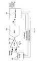
- the pixel array 11 previously shown in FIG. 4 and tabulated in FIG. 5is centrally embedded within imaging System-on-Chip 10 .
- FIG. 6shown for clarity in FIG. 6 is a simplified six-by-six pixel array 11 including thin OB border having illustrated width of only one pixel.
- Pixel block 11is read through Column Buffer 16 and multiplexed into a serial analog data stream by horizontal multiplexer 18 under the direction of iSoC Supervisor 12 .
- Supervisor 12generates the various timing and control signals that stimulate all iSoC blocks at the appropriate times.
- Each Column Buffer in 16conditions the analog data from each column of pixels using, for example, the schematic and methodology taught by U.S. Pat. No. 5,892,540.
- the serial analog data stream including both OB and photo-generated pixel datais supplied to the circuit of the present invention, Stabilization Block 100 .
- the present inventionis a mixed-signal System-on-Chip solution, i.e., both analog and digital circuits, comprising the five internal circuit blocks included in Stabilization block 100 and commonly serviced by signal bus 900 .
- a digital data streamis supplied by signal bus 900 and finally output from the sensor via I/O Port 600 .
- Digitization block 200consists of Programmable Gain Amplifier (PGA) 210 and high resolution A/D converter 220 that successively black-clamp, amplify and digitize the analog signal stream to at least 12 bits resolution.
- PGA 210accepts an analog correction signal from BlackClamp block 500 to perform black-clamping.
- General purpose black level clamping to a preset value(set by the programming register) is hence performed via the feedback loop facilitated by the digital signal processing in BlackClamp 500 .
- the multiple (usually 3 or 4) colorscan be alternately handled by a single signal processing chain or alternately segregated using multiple Digitization blocks 200 .
- Analog dynamic rangeis maximized in either case by minimizing black level dispersion prior to digitization.
- Column noisewhich is typically less than several LSBs peak-to-peak, is then digitally removed in Column Noise Correction block 300 with support from Column Correction Memory 320 , which preferably stores offset differences. Correction of line-to-line noise is finally completed in Line Noise Correction block 400 , which also preferably stores difference values.
- the collective correctionsinsure that a flicker-free stream of digitized image data is supplied to the camera via I/O port 600 .
- the OB reference data used by the present inventioncomprises a stream of OB pixels averaged over a programmable number of OB rows and/or OB columns to accurately determine and dynamically adjust the black reference level.
- FIG. 7shows the front porch of a representative pixel stream for a line of video comprising 4 black pixels, followed by a programmable time interval denoted BLACKWAITTIME, and a second set of 4 black pixels.
- the epoch spanning the first group of 4 black pixelsis labeled AVEPIX and refers to the number of OB pixels used to average the preliminary OB information.
- the BLACKWAITTIMEis used to perform signal processing operations on the data in the intervening clock cycles.
- the correctionis allowed to settle during the programmable BLACKWAITTIME and/or after the second OB block is read.
- a second “push down” or “push up” correctionfurther adjusts the sensor's black level at this time.
- the iterative process of reading OB pixels, adjusting the black level, reading additional OB pixels, and then readjusting the black levelenables the black clamping feedback loop to accurately converge to the appropriate black reference target prior to the actual time that the initial active video enters the iSoC video stream.
- the iterative processalso prevents transients from corrupting the black reference level generated by the black-clamping loop.
- the clear and OB pixelsare further segregated into sets of “clear” pixels and “black” pixels as revealed in FIG. 8 .
- the clear pixelswhich are included in the region labeled ClearPixels, are the light-sensitive elements that form the visual electronic image.
- the black pixelswhich are included in regions R 1 _OB, R 1 _OBC, R 2 _OB, RW_OBC and R 3 _OB, are insensitive to light. Black pixels in regions R 1 _OB, R 2 _OB and R 3 _OB are used to remove line noise on a line-by-line basis; black pixels in regions R 1 _OBC and R 2 _OBC are used to determine column offset coefficients for black reference and active pixels, respectively. Black pixels in region R 1 _OB and R 2 _OB are used in combination with pixels in region R 3 _OB to perform black clamping.
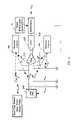
- a preferred embodiment of the present inventionis further illustrated in the schematic circuit diagram of FIG. 9 .
- the architectureis extensible to multiple signal paths and specific exclusion or programmable enabling/disabling of any of the blocks.
- the sensor data that is output from I/O Port 600consists only of black-clamped and digitized data.
- the preferred embodimentshows one signal path supported by black-clamping, line noise suppression and column noise suppression, multiple signal and noise suppression paths can similarly be supported in alternative embodiments.
- the schematic diagram in FIG. 12shows two data paths having black-clamp operation and line noise correction.
- the first offset correctionis the general black-clamping via the PUSHUP PUSHDOWN STRONGPUSH adjustment at the input of PGA 210 , which is facilitated by BlackClamp 500 .
- the secondis the LineOffsetT 1 adjustment calculated by Line Noise Correction block 400 that is supplied to Summing Block 410 to remove line noise.
- the third offset correctionis the ColumnNoiseOffset adjustment generated by Column Noise Correction Block 300 and supplied to Summing Block 310 to remove column noise.
- the previously described stepsare performed by tapping digital data from signal bus 900 , which is preferably at least 18 bits wide, and subsequently reinserting the corrections as shown.
- the main data flowfollows the path of bus 900 and BlackClamp block 500 is the first iSoC signal processing block to tap the signal to stabilize the black level.
- Summing block 510buffers the tapped video stream and supplies the latest data to Register 520 .
- Comparator 530compares the latest information to the target value BlackRef_T 1 and, depending on whether quick convergence is needed, as dictated by the programmed setting for register value strongref, an incremental amount of push-up, push-down, or a stronger push-up/push-down is performed.
- FIG. 10illustrates a block diagram for a first embodiment of the general black-clamping feedback loop wherein a digitally-controlled charge pump 230 is used to perform the push up, push down or strong push of the analog correction signal controlled by digital means.
- a preferred embodiment shown in FIG. 11alternatively uses a cross-coupled DAC 240 as described in related U.S. Patent application No. TBD, entitled, CROSS-COUPLED DIFFERENTIAL DAC-BASED CLAMP CIRCUIT.
- two DACsare used in tandem to sustain fine and coarse adjustment of the black clamp correction terms.
- the coarse and fine correction voltagesare supplied to PGA 210 through identical coupling capacitance, C bc .
- Green pixels in a row of red and green pixelsis thus often distinguished and labeled as an G R pixel.
- a green pixel in a row comprising green and blue pixelsis similarly considered to be an G B pixel.
- the register control block 64thus may have pre-programmed gain settings for a given image sensor's color filter array, and/or may be dynamically adjusted based on settings from the camera.
- the iSoC data stream including reference and active pixel dataare supplied to the input of PGA 610 whose gain is set, on a pixel-by-pixel or channel-by-channel basis, by iSoC register control 64 .
- the final outcomeis that the resulting output signal from the digital controller is dynamically governed to generate the output signal:
- V outC sig C f ⁇ V sig + C bc C f ⁇ V bc
- V outis the output signal
- V sigis the active pixel signal
- V bcis the optical black pixel signal
- C sigis the capacitor setting for the active video
- C bcis the capacitor setting for the black clamp data stream
- C fis the base feedback capacitance.
- the present inventionhence allows separate gain for the active and black pixels in addition to separate gain for each color.
- additional capacitorscan be used to increase the total range of gain control including support for cross-coupled Digital-to-Analog Converter (DAC) 66 .
- DACDigital-to-Analog Converter
- four PGAscan be used to best handle the G R , G B , R or B channels. Then, for example, the G R , G B , R or B channels are subsequently recombined in the desired order in I/O port 600 .
- the iSoC data streamis digitized by the Analog-to-Digital Converter (ADC) 220 , which preferably provides a minimum resolution of 12 bits to maximize the accuracy of generating the highest purity black reference level. Digitized data is then supplied to BlackClamp block 500 which compares the black level data to the target black level 72 , BLACKREF. Any differences in the two levels are fed back to the DAC. Depending on whether the target is offset by a small or large amount, or whether the difference is positive or negative, the digital controller appropriately controls the DAC to supply the correct offset to the other leg of the PGA.
- ADCAnalog-to-Digital Converter
- the average black level valueis hence compared to BLACKREF in the logic embedded in BlackClamp Block 500 which determines whether to shift UP or DOWN by a small amount, or UP or DOWN by a large amount if the difference exceeds a second threshold, STRONGREF, so as to trigger correction of the black level by DAC 240 :
- FIGS. 13A through 13Flists an implementation of Verilog code implementing BlackClamp block 500 .
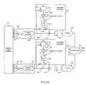
- Line Noise Correction block 400receives the composite (imaging+OB pixels) data stream from the signal bus, accumulates the data and then stores the accumulated data in summing register 430 . Each register in the data path results in one cycle of latency. The pixel values are accumulated in register 430 and averaged in divider 440 (division through bit shifts). The resulting LineOffset and LineAve values are further used by the line noise correction block 400 to complete line correction and also supplied output to the column noise correction block 300 at Multiplexer 830 . Summing register 430 feeds the running total back to summing node 420 until the programmed number of black reference pixels are used.
- the operating modes of the Line Noise Correction Block 400are programmably controlled by the register settings tabulated in FIG. 14 and implemented as described.
- the line noiseis alternately removed using three algorithms that are optimized to correct for temporal line-to-line variation in the image for various types of sensor setup, camera setup or imaging conditions.
- the black pixels of each roware read out, accumulated and averaged; the resulting line average (LineAve) is then used to determine the line offset relative to the programmed target or reference.
- This line offset (LineOffset)is subtracted from subsequent (clear) pixels in the row.
- the general form for line average and line offset for row Ris given as:
- LineOffset RLineBlackRef - LineAve R ,
- N BLKis the number of black pixels counted.
- STOPADDR_DARKis the stop address and STARTADDR_DARK is the starting address for the OB pixels to be used by the algorithmic processing.
- the actual number of black pixels used in the signal processing operationis thus NumPixelBlack* 32 .
- the expressions for line offsetsare:
- LineOffset T1round(LineBlackRef ⁇ LineAve T1 ),
- LineOffset T2round(LineBlackRef ⁇ LineAve T2 ),
- LineOffset B1round(LineBlackRef ⁇ LineAve B1 ),
- LineOffset B2round(LineBlackRef ⁇ LineAve B2 )
- LineBlackRefis a 12-bit register value (see register descriptions above) supplied to Subtractor 450 for effecting the desired line noise correction.
- the process of calculating the line offset coefficientsstarts by reading the OB pixels and calculating the average dc value, 1(r), each and every frame such that:
- the Column Noise Correction Block 300implements an algorithm to correct for column-based fixed pattern noise (FPN) in the image.
- FIG. 16illustrates an ideal scenario.
- the correction algorithmuses memories to store an offset associated with each column, as compared to a desired reference. These offsets are first calibrated during the black rows, written into a memory, and then read out and applied to the clear pixels of the image sensor in order to correct for FPN.
- calculating the offsets for the black rowsinvolves using a push/pull algorithm.
- a “reference”which is generated by Line Noise Correction 400 block. If the value of the pixel is too high with respect to the reference, the value needs to lowered, or if the value is too low, it needs to be raised.
- the amount added or subtractedis a programmable “push/pull” value, typically, 1 , 8 or 16 . With multiple rows (i.e. 128 per frame), the add/subtract calculation will be made multiple times. The value accumulates, and is stored in a memory.
- each add/subtract operationis actually a “read/modify/write” operation with respect to the memory.
- the comparisonis made, and the memory offset is then modified, and then re-written to memory. This is done on a per-column basis for the pixels in the array.
- the appropriate offsetsare calculated in the black rows, they are then applied to the corresponding clear pixels. Again, the corresponding offset is read from memory, and added to the clear pixel. Note that since the value in memory can either be positive or negative, the resulting pixel value with either be higher or lower—depending on which direction the pixel needs to be corrected (as illustrated in FIG. 16 ).
- column noiseis removed by Column Noise Correction Block 300 to support the implementation result illustrated in FIG. 16 , wherein black level dispersion in the video stream is reduced from the order of 100 ⁇ V in the analog domain to well below 1 LSB irrespective of the gain implemented in the end-to-end signal chain along signal bus 900 .
- the correction algorithmuses blocks of memory in Column Correction Memory 320 to store the noise coefficient for each column relative to a desired target reference. These column noise coefficients are first determined during the vertical blanking interval when black rows are read, subsequently written into the respective memory banks, and finally read out as a black clamping correction signal, which is labeled ColumnNoiseOffset in FIG. 9 , and applied in the clear region of the image to correct for column noise via summing block 310 .
- the black reference used for calibrationcan be a fixed value set by the user, or it can be the line average calculated using the OB pixels in each row. If the line average is used as the reference, then the values stored in the memory are better representations of a true set of column noise.
- the shaded regionsindicate the OB rows and OB columns at the sensor perimeter.
- column noise correctionthe process of reading and adding FPN memory content to pixel values
- R 1 _OBC, R 2 _OBC, and ClearPixelsThis process entails reading memory 320 and adding the offset coefficients to the corresponding pixel values.
- register OFFSET_CLAMPENif register OFFSET_CLAMPEN is set to 0, column noise calibration is performed in both R 1 _OBC, and R 2 _OBC. If register OFFSETWRITE_ALLROWS is set to 1, then FPN calibration is performed in regions R 1 _OBC, R 2 _OBC, and ClearPixels.
- the comparatorchecks the sum of the present pixel value, p(r, c), and its most recent column offset coefficient, o(r ⁇ 1), to determine when the sum is greater than the line average, 1(r) and appropriately decide need for correction.
- the logic operation for determining such needis:
- 1(r)can be a fixed threshold like the target black reference value, blackref.
- 1(r)can be selected as the average calculated in the black columns during line noise correction.
- the present inventionincludes a computer program product which is a storage medium (media) having instructions stored thereon/in which can be used to control, or cause, a computer to perform any of the processes of the present invention.
- the storage mediumcan include, but is not limited to, any type of disk including floppy disks, mini disks (MD's), optical discs, DVD, CD-ROMS, CDRW ⁇ , micro-drive, and magneto-optical disks, ROMs, RAMs, EPROMs, EEPROMs, DRAMs, VRAMs, flash memory devices (including flash cards, memory sticks), magnetic or optical cards, MEMS, nanosystems (including molecular memory ICs), RAID devices, remote data storage/archive/warehousing, or any type of media or device suitable for storing instructions and/or data.
- the present inventionincludes software for controlling both the hardware of the general purpose/specialized computer or microprocessor, and for enabling the computer or microprocessor to interact with a human user or other mechanism utilizing the results of the present invention.
- softwaremay include, but is not limited to, device drivers, operating systems, and user applications.
- computer readable mediafurther includes software for performing the present invention, as described above.
Landscapes
- Engineering & Computer Science (AREA)
- Multimedia (AREA)
- Signal Processing (AREA)
- Transforming Light Signals Into Electric Signals (AREA)
Abstract
Description
- The present invention is related to: U.S. patent application Ser. No. TBD, entitled, “CROSS-COUPLED DIFFERENTIAL DAC-BASED CLAMP CIRCUIT,” filed TBD; U.S. patent application Ser. No. TBD, entitled, “ON-CHIP BLACK CLAMPING CIRCUIT FOR CMOS IMAGE SENSOR,” filed TBD; and U.S. patent application Ser. No. TBD, entitled, “METHOD FOR BLACK CLAMP CORRECTION INDEPENDENT OF GAIN,” filed TBD; the disclosures of which are herein incorporated by reference.
- A portion of the disclosure of this patent document contains material which is subject to copyright protection. The copyright owner has no objection to the facsimile reproduction by anyone of the patent document or the patent disclosure, as it appears in the Patent and Trademark Office patent file or records, but otherwise reserves all copyright rights whatsoever.
- 1. Field of the Invention
- The present invention relates generally to electronic imaging sensors and, specifically, to advanced imaging system-on-chip (iSoC) sensors having embedded signal processing functions.
- 2. Description of the Related Art
- Imaging sensors operate by collecting light intensity in a contiguous array of imaging pixels. Each pixel will have a charge proportional to the intensity of the light incident on the pixel over the duration of exposure. This charge is a “pixel value” that must be read out with as little noise as possible to capture a high quality image or generate video. Although modem CMOS sensors have lower temporal noise than CCD imaging sensors at data rate >25 MHz, several sources of systematic artifacts can degrade image quality, especially at low illumination.
- Readout of the image electronically reproduced in CMOS imaging sensors is achieved by routing the signal from each row of pixels through a set of column buffers to the output as shown in
FIG. 1 from U.S. Pat. No. 6,861,634. Eachcolumn buffer 102 normally supports a specific column of pixels and is constructed using an integrated amplifier block such as taught in U.S. Pat. No. 5,892,540. Although circuit block70 inFIG. 2 from '540 corrects column buffer offsets in the analog domain to about 100 μV rms as compared to a full-scale signal on the order of 1V, i.e., one part in 104, maximizing image quality mandates further reducing “column noise.” Likewise, because each video line is read at a different time than either the prior or next line, the readout process can introduce “line noise.” Furthermore, the supporting column buffers use common reference voltages (such as REF1, REF2 and REF3 inFIG. 2 ) that carry intrinsic noise with time-varying characteristics. Since each row of pixels is sampled at the same time, each row of pixels samples the common reference noise at similar aggregate value. On the other hand, subsequent rows are interrogated at different times and thus sample the common references at slightly different collective values. This row-to-row variability generates “line noise” and frame-to-frame “flicker.” All these possible noise mechanisms degrade image quality via the following deleterious effects: - 1. Vertical stripes that are set and can dynamically fluctuate on a column-to-column basis.
- 2. Horizontal stripes that are set and can dynamically fluctuate on a line-to-line basis, i.e., line noise wherein each line is a horizontal stripe of pixels.
- 3. Frame-to-frame instability that is a by-product of an image sensor's sensitivity to reference noise. The sensitivity effectively destabilizes the sensor's black level on a frame-by-frame basis since vertical blanking time is significantly longer than horizontal blanking time. Hence, black reference behavior is strongly frame-dependent.
In high performance imaging sensors, the most distracting effect is frame-to-frame instability.
- In the prior art, U.S. Pat. No. 5,172,249 subtracts amplifier offsets and FPN by applying signal and reference levels to the input of a subtraction circuit, such as a differential amplifier, without due consideration for the deleterious impact of wideband noise in causing offset correction errors. U.S. Pat. No. 6,037,577 alternatively provides means to suppress row noise on a row-by-row basis. However, the primary intent is again to suppress offsets from switching noise and charge redistribution among the parallel signal paths rather than to eliminate discretely sampled common reference noise.
- U.S. Pat. No. 6,861,634 subsequently teaches a technique for subtracting reference noise in addition to other sources of sensor noise. The noise subtraction is performed in the analog domain using a correction value previously determined in the digital domain. The analog value is supplied to a sample-and-hold circuit including a charge amplifier for subtracting the offset. The preferred embodiment teaches pseudo-differential or differential signal paths using the pixel's signal level and associated reset level. Unfortunately, burdening the signal path by also supplying the reset level to the offset-subtracting amplifier halves the maximum video rate, doubles the concomitant video bandwidth, and boosts white noise. The correction is also carried out at high speed on a pixel-by-pixel and per-color basis, thus increasing complexity and signal processing overhead.
- Recently, U.S. Patent Application Publication No. 2006/0231734 teaches wholly digital means to determine and correct column fixed pattern noise. This effectively limits accuracy of the various corrections rather than enhancing the analog dynamic range presented for A/D conversion.
- The present invention includes a method, circuit implementation and firmware code that together provide superior black level stabilization. Analog circuits, digital circuits, and algorithms jointly suppress the various fixed pattern noise sources inherent in “reading out” arrays of image-sensing pixels, while simultaneously maximizing the dynamic range in the analog domain. In a preferred embodiment, the noise suppression is performed in the digital domain using algorithms specifically optimized to produce electronic images with useful image quality spanning at least16 bits of dynamic range, even though only 12 bits may be supplied to the camera from frame-to-frame.
- In one embodiment, the present invention comprises an apparatus for processing a signal output from a pixel array, the pixel array having optical black pixels and active clear pixels, the apparatus comprising a black clamp block, wherein the black clamp block receives an output signal from the pixel array, compares a black level from the output signal to a black reference value, and outputs an adjustment signal based on the comparison to adjust a black level in the output signal;
- a line noise correction block, wherein the line noise correction block receives the output signal adjusted by the black clamp block, calculates a line noise average value for black pixels in the output signal on a line-by-line basis, calculates a line noise offset based on a difference between the line noise average and the black reference value, and applies the line noise offset to clear pixels in the output signal; and
- a column noise correction block, wherein the column noise correction block calculates a column noise offset for black pixels in the output signal, and applies the column noise offset to the clear pixels in the output signal;
- wherein the column noise offset is calculated on a column basis by comparing the output signal for each black pixel with the line noise average value calculated by the line noise correction block.
- The apparatus may further comprise a column noise correction memory, the memory storing column noise offset coefficients, wherein the column noise offset coefficients are updated using a differential technique, such that coefficients stored in the memory represent a difference of column noise relative to line noise.
- Another embodiment of the present invention comprises a signal processing circuit for processing an output signal from a pixel array, the pixel array having optical black pixels and active clear pixels, the circuit comprising a differential programmable gain amplifier, one input of the differential programmable gain amplifier connected to the output signal from the pixel array;
- an analog-to-digital converter connected to the differential programmable gain amplifier, wherein the analog-to-digital converter converts an output signal from the programmable gain amplifier into a digitized output signal;
- a black clamp processing block connected to the analog-to-digital converter, wherein the black clamp processing block compares the digitized output signal with a black reference value, and outputs a black level adjustment signal to an input of the programmable gain amplifier;
- a line noise correction processing block connected to the analog-to-digital converter, wherein the line noise correction processing block calculates a line noise average value for black pixels in the output signal on a line-by-line basis, and calculates a line noise offset based on a difference between the line noise average value and the black reference value;
- a column noise correction processing block, wherein the column noise correction processing block calculates a column noise offset for black pixels in the digitized output signal, the column noise offset calculated on a column basis by comparing the digitized output signal for each black pixel with the line noise average value calculated by the line noise correction processing block;
- a first adder to add the column noise offset to the clear pixels in the digitized output signal; and
- a second adder to add the line noise offset to the clear pixels in the digitized output signal.
- The circuit of the present invention may further comprise a column noise correction memory, the memory storing column noise offset coefficients, wherein column noise offset coefficients are updated using a differential technique, such that coefficients stored in the memory represent a difference of column noise relative to line noise.
- According to one embodiment, a method of the present invention includes a method to process an output signal from a pixel array, the pixel array having optical black pixels and active clear pixels, the method comprising:
- calculating a black level adjustment signal, wherein calculating the black level adjustment signal comprises:
- comparing an output signal from the pixel array with a black reference value;
- calculating a line noise correction value, wherein calculating the line noise correction value comprises:
- calculating a line noise average value; and
- comparing the line noise average value to the black reference value;
- calculating a column noise correction value; wherein calculating the column noise correction value comprises:
- comparing the digitized output signal for each black pixel with the line noise average value calculated by the line noise correction processing block;
- adjusting a black level in the output signal according to the black level adjustment signal to form a second output signal;
- adding the column noise correction value to the second output signal to form a third output signal; and
- adding the line noise correction value to the third output signal. The method may further includes storing column noise offset coefficients in a memory and updating them using a differential technique, such that the coefficients stored in the memory represent a difference of column noise relative to line noise.
- The present invention will be readily understood by the following detailed description in conjunction with the accompanying drawings, wherein like reference numerals designate like structural elements, and in which:
FIG. 1 is a block diagram of a prior art CMOS APS system with digital correction terms applied via analog circuits from U.S. Pat. No. 6,861,634;FIG. 2 is a schematic diagram of a prior art column buffer taught in U.S. Pat. No. 5,892,540;FIG. 3 is a block diagram of a prior art architecture for processing output from an image sensor;FIG. 4 is a block diagram showing a representative embodiment of a sensor array including active pixels, black reference or optically black (OB) pixels, dummy pixels and guard bands;FIG. 5 is a table articulating the structure of the sensor array partitioned inFIG. 3 and shown in schematic circuit form inFIG. 6 ;FIG. 6 is a block diagram of an embodiment of the present invention integrated in a typical imaging System-on-Chip sensor;FIG. 7 is a diagram of the imaging System on Chip data stream that specifically shows the output of the black reference pixels and the time intervals for updating the sensor's black reference level;FIG. 8 is a block diagram of the pixel array of the present invention including the black pixel regions and active clear pixel regions;FIG. 9 is a schematic diagram of a preferred embodiment of the present invention including support for black-clamping, line noise suppression and column noise suppression;FIG. 10 is a schematic diagram of an embodiment of the present invention incorporating a digitally-controlled charge pump as analog black clamping circuit;FIG. 11 is a schematic diagram of a preferred embodiment of the present invention incorporating programmable DAC as analog black clamping means disclosed in related U.S. patent application Ser. No. TBD, entitled, CROSS-COUPLED DIFFERENTIAL DAC-BASED CLAMP CIRCUIT;FIG. 12 is a schematic diagram of an embodiment of the present invention including support for two data channels;FIG. 13A begins a listing of an implementation of the Verilog code for general black clamping inBlackClamp Block 500;FIG. 13B continues the code ofFIG. 13A ;FIG. 13C continues the code ofFIG. 13B ;FIG. 13D continues the code ofFIG. 13C ;FIG. 13E continues the code ofFIG. 13D ;FIG. 13F completes the Verilog code for implementingBlackClamp Block 500 listed inFIGS. 13A through 13E ;FIG. 14 lists the programming registers pertaining to line noise suppression;FIG. 15A is a table of the algorithms for LineNoiseMode=1;FIG. 15B is a table of the algorithms for LineNoiseMode=2;FIG. 15C is a table of the algorithms for LineNoiseMode=3 or 0; andFIG. 16 illustrates the effect of column noise correction as it is applied to a row (line) of pixels.- The following description is provided to enable any person skilled in the art to make and use the invention and sets forth the best modes contemplated by the inventor for carrying out the invention. Various modifications, however, will remain readily apparent to those skilled in the art. Any and all such modifications, equivalents and alternatives are intended to fall within the spirit and scope of the present invention.
- In general, conventional image sensors consist of a pixel array that outputs an image signal, and digital imaging processing blocks that are designed to increase the quality of the resulting image. Currently, there are three general types of processing algorithms used: black clamping, line noise correction, and column fixed pattern noise (FPN) correction. Historically, these algorithms have been deployed in a separate and discrete fashion, with each algorithm operating independently of the others (see
FIG. 3 ). The present invention, however, as described below, overcomes the limitations of the prior art, and provides an architecture that shares information between the processing blocks (algorithms). This provides several advantages including faster convergence of the digital algorithms, higher quality image output, and possibly smaller circuitry. - The present invention includes a representative design for an active-pixel CMOS imager. A prototype embodiment of the low-noise active pixel sensor (APS) invention can be constructed, for example, as a visible imager comprising an active array of 4096 (columns) by 3072 (rows) of visible light detectors (photodetectors). The active array, or nominal record area, is bounded by black reference pixels in the surrounding periphery.
FIG. 4 is an array plan showing a nominal record area enclosed by a perimeter of optical black (OB), guard band, dummy, and optional optical alignment pixels. - The rows and columns of pixels can be spaced4 microns center-to-center using 0.18 μm design rules to provide as-drawn optical fill factor of ˜50% for each pixel without microlens. Several columns and rows of detectors at the perimeter of the light-sensitive region are normally covered with metal and/or other opaque material layers to form the OB pixels. Constantly reading the OB pixels during the various blanking intervals, i.e., time segments during which photo-generated data is not supplied by the sensor, enables the present invention to update and stabilize the black level. The black level stabilization of the present invention includes three types to maximize sensor performance over wide range in sensor temperature and environment. The stabilization modes include: 1) general black-level clamping; 2) fine-tuning of black level on a line-by-line basis to compensate line noise with appropriate line-based coefficients, and; 3) fine-tuning of black level on a column-by-column basis to adjust for column noise.
- The light-sensitive detectors in each row can be covered with color filters to produce color imagers. For example, the odd rows may begin at the left with red, green, then blue filters, and the even rows may begin with blue, red, then green filters, with these patterns repeating to fill the respective rows. A standard Bayer filter pattern can also be applied. The video signal from the active pixel sensor hence includes:
- a first interval of light-insensitive pixels comprising at least a portion of the Optical Black (OB) border surrounding the active imaging region and other non-imaging pixels
- a second interval of light-sensitive imaging pixels comprising the bulk of the image sensor's data stream for electronic capture or viewing
- optionally, a third interval of OB pixels
- As previously discussed, it is not required to read the various pixel data at a specific time. For example, all black pixels can be read during the “front porch” of the aggregate data stream including data from the black and active pixels of each line of the imaging sensor. The active pixels, however, are often read during a continuous interval preceded by a “front porch” and followed by a “back porch” as defined by various timing standards such as, e.g., SMPTE 274M or SMPTE 292 specifications for high definition video, herein incorporated by reference. The term “porch” refers to an interval during each video line, field or frame, wherein actual imaging data is not being supplied to the camera and overhead signal processing functions can instead be performed. Such blanking intervals were originally required for CRT displays for beam flyback. The relevant OB pixel data can all be read during the front porch, split between front porch and black porch, or altogether read during the back porch. While the OB data stream is always sent to the digital controller supervising all operations and signal processing in the imaging System-on-Chip (iSoC), it can also be provided to the camera in a composite data stream. Providing a stable black reference to the camera enables highest quality image capture and possible further processing.
- The table in
FIG. 5 further articulates the composition of active and supporting pixels in both the horizontal and vertical directions for a typical embodiment. In the horizontal direction, for example, a sensor supporting a base resolution of 4096 by 3072 pixels actually encompasses a grand total of 4416 by 3300 pixels of which 4352 by 3252 are addressable for readout. The additional rows and columns along the perimeter are required to enhance image quality via electrical isolation and iSoC image processing. Specifically, the pixels adjacent to the surrounding iSoC circuits constitute a guard band that is 24 pixels wide thus spanning a buffer region of about 100 μm (i.e., 41 m×24 pixels) to isolate electronic circuit operations from photo-electronic functions. The primary role of the guard band pixels is to block indirect light or stray photogenerated carriers from reaching the electronic circuits via the substrate since the free carrier absorption length in silicon is typically about 100 μm. Another key objective is to prevent electromagnetic interference caused by iSoC operation in the peripheral electronic circuits from corrupting the signal in OB and clear pixels. Next in the pixel arrangement are various sets of OB pixels including a first dummy region (OB dummy1) spanning eight pixels, 64 OB pixels to stabilize the black level via the present invention, a second OB dummy region comprising 12 pixels, 12 clear dummy pixels to separate OB from active, 32 fully active pixels useful for compensating for sensor-to-camera misalignment by accordingly shifting the nominal record area, 8 boundary process pixels also used for special signal processing operations, the main span of 4096 fully active pixels, and an optional matching set of supporting pixels on the opposite side of the nominal record area. - In a preferred embodiment illustrated in
FIG. 6 , thepixel array 11 previously shown inFIG. 4 and tabulated inFIG. 5 is centrally embedded within imaging System-on-Chip 10. Rather than the full-sized array comprising 4416 by 3300 pixels, shown for clarity inFIG. 6 is a simplified six-by-sixpixel array 11 including thin OB border having illustrated width of only one pixel.Pixel block 11 is read throughColumn Buffer 16 and multiplexed into a serial analog data stream byhorizontal multiplexer 18 under the direction ofiSoC Supervisor 12.Supervisor 12 generates the various timing and control signals that stimulate all iSoC blocks at the appropriate times. Each Column Buffer in16 conditions the analog data from each column of pixels using, for example, the schematic and methodology taught by U.S. Pat. No. 5,892,540. - Next, the serial analog data stream including both OB and photo-generated pixel data, is supplied to the circuit of the present invention,
Stabilization Block 100. The present invention is a mixed-signal System-on-Chip solution, i.e., both analog and digital circuits, comprising the five internal circuit blocks included in Stabilization block100 and commonly serviced bysignal bus 900. After analog processing, digitization, and digital processing are performed in the present invention, a digital data stream is supplied bysignal bus 900 and finally output from the sensor via I/O Port 600. - While raw analog video is viewable by carefully monitoring the data stream supplied by
Horizontal Multiplexer 18,Stabilizer 100 amplifies and digitizes the analog video inDigitizing Block 200.Digitization block 200 consists of Programmable Gain Amplifier (PGA)210 and high resolution A/D converter 220 that successively black-clamp, amplify and digitize the analog signal stream to at least12 bits resolution. In addition to amplifying the analog video,PGA 210 accepts an analog correction signal fromBlackClamp block 500 to perform black-clamping. General purpose black level clamping to a preset value (set by the programming register) is hence performed via the feedback loop facilitated by the digital signal processing inBlackClamp 500. In usingPGA 210 to perform both amplification and black-clamping, the multiple (usually 3 or 4) colors can be alternately handled by a single signal processing chain or alternately segregated using multiple Digitization blocks200. Analog dynamic range is maximized in either case by minimizing black level dispersion prior to digitization. Column noise, which is typically less than several LSBs peak-to-peak, is then digitally removed in Column Noise Correction block300 with support fromColumn Correction Memory 320, which preferably stores offset differences. Correction of line-to-line noise is finally completed in Line Noise Correction block400, which also preferably stores difference values. The collective corrections insure that a flicker-free stream of digitized image data is supplied to the camera via I/O port 600. - The OB reference data used by the present invention comprises a stream of OB pixels averaged over a programmable number of OB rows and/or OB columns to accurately determine and dynamically adjust the black reference level.
FIG. 7 shows the front porch of a representative pixel stream for a line of video comprising 4 black pixels, followed by a programmable time interval denoted BLACKWAITTIME, and a second set of 4 black pixels. The epoch spanning the first group of 4 black pixels is labeled AVEPIX and refers to the number of OB pixels used to average the preliminary OB information. The BLACKWAITTIME is used to perform signal processing operations on the data in the intervening clock cycles. Shown is the ability to “push up” or “push down” the active video by incrementing or decrementing the black level (PUSHUP or PUSHDOWN) just after reading each OB segment. The correction is allowed to settle during the programmable BLACKWAITTIME and/or after the second OB block is read. After subsequently reading a second set of OB pixels, a second “push down” or “push up” correction further adjusts the sensor's black level at this time. Hence, the iterative process of reading OB pixels, adjusting the black level, reading additional OB pixels, and then readjusting the black level enables the black clamping feedback loop to accurately converge to the appropriate black reference target prior to the actual time that the initial active video enters the iSoC video stream. The iterative process also prevents transients from corrupting the black reference level generated by the black-clamping loop. - The clear and OB pixels are further segregated into sets of “clear” pixels and “black” pixels as revealed in
FIG. 8 . The clear pixels, which are included in the region labeled ClearPixels, are the light-sensitive elements that form the visual electronic image. The black pixels, which are included in regions R1_OB, R1_OBC, R2_OB, RW_OBC and R3_OB, are insensitive to light. Black pixels in regions R1_OB, R2_OB and R3_OB are used to remove line noise on a line-by-line basis; black pixels in regions R1_OBC and R2_OBC are used to determine column offset coefficients for black reference and active pixels, respectively. Black pixels in region R1_OB and R2_OB are used in combination with pixels in region R3_OB to perform black clamping. - A preferred embodiment of the present invention is further illustrated in the schematic circuit diagram of
FIG. 9 . The architecture is extensible to multiple signal paths and specific exclusion or programmable enabling/disabling of any of the blocks. When signal processing blocks300 and400 are disabled, for example, the sensor data that is output from I/O Port 600 consists only of black-clamped and digitized data. While the preferred embodiment shows one signal path supported by black-clamping, line noise suppression and column noise suppression, multiple signal and noise suppression paths can similarly be supported in alternative embodiments. The schematic diagram inFIG. 12 , for example, shows two data paths having black-clamp operation and line noise correction. - As previously introduced, three black level correction operations are performed in the preferred embodiment, including general black clamping, specific column noise correction and specific line noise correction. Three dc offset adjustments are hence performed in the signal processing flow to support specific target values for each operation. The first offset correction is the general black-clamping via the PUSHUP PUSHDOWN STRONGPUSH adjustment at the input of
PGA 210, which is facilitated byBlackClamp 500. The second is the LineOffsetT1 adjustment calculated by Line Noise Correction block400 that is supplied to SummingBlock 410 to remove line noise. The third offset correction is the ColumnNoiseOffset adjustment generated by ColumnNoise Correction Block 300 and supplied to SummingBlock 310 to remove column noise. A fourth offset correction, OFFSET_T1, is optionally supplied to SummingBlock 710 to adjust the black level target within the dynamic range supported onsignal bus 900. The black level stabilization processes including general black clamping, line noise correction and column noise correction operations are performed as follows: - 1. Determine and update the black level by first using the black row data in optical black region R1_OB. This step removes any systematic offsets generated by the analog readout path and subsequently refines the column noise data calculated using region R1_OBC. The sensor can be read by either starting at the top or starting at the bottom; R1_OB and R1_OBC regions are hence available both at the top and bottom.
- 2. Continue updating black reference level using region R2_OB. Compute the average line noise in each row using optical black region R2_OBC. Remove line noise prior to determining each column's dispersion coefficient.
- 3. Update column noise coefficients using differential technique wherein the coefficients stored in memory do not represent the absolute value but rather the difference of the column noise relative to the line noise. The offset coefficients are accumulated over several rows with different algorithmic weight. The differential approach is significantly more powerful than accumulation since it is insensitive to the line noise present in the actual OB rows used to determine the column noise coefficients. By employing a differential technique, the line noise average also provides a thresholding basis to more accurately determine each column's offset coefficient. The OB rows are consequently split into R2_OB to compute line noise and R2_OBC to compute column noise in the absence of the line noise computed during the R2_OB interval.
- 4. As readout enters rows with active pixels, compute each line's average noise using optical black region R3_OB.
- 5. When reading the ClearPixel region, i.e., active pixels in the nominal record area, remove line noise using the data computed by processing R3_OB.
- 6. Update the black reference using either or both R3_OB regions, depending on how the sensor is used and appropriately programmed.
- 7. Update column offset coefficients using R2_OBC data after correction for line noise using R2_OB information.
- 8. Since there are a limited number of optically black pixels in each region, anomalous pixels are identified and subsequently ignored during the calculations to further improve accuracy of black-clamping, column noise and line noise correction.
- For the representative case of a single video chain, the previously described steps are performed by tapping digital data from
signal bus 900, which is preferably at least18 bits wide, and subsequently reinserting the corrections as shown. The main data flow follows the path ofbus 900 and BlackClamp block500 is the first iSoC signal processing block to tap the signal to stabilize the black level. Summingblock 510 buffers the tapped video stream and supplies the latest data to Register520.Comparator 530 compares the latest information to the target value BlackRef_T1 and, depending on whether quick convergence is needed, as dictated by the programmed setting for register value strongref, an incremental amount of push-up, push-down, or a stronger push-up/push-down is performed. The black level is subsequently corrected by supplying the associated analog signal, labeled PUSHUP PUSHDOWN STRONGPUSH inFIG. 9 , toPGA 210 ofDigitization Block 200. In this manner, the digital logic controls an analog operation to maximize the analog dynamic range for subsequent digitization. The result is that the analog black clamping signal stabilizes the black reference level of the image data stream. Further black clamping is performed by subsequently suppressing line noise and column noise. FIG. 10 illustrates a block diagram for a first embodiment of the general black-clamping feedback loop wherein a digitally-controlledcharge pump 230 is used to perform the push up, push down or strong push of the analog correction signal controlled by digital means. A preferred embodiment shown inFIG. 11 alternatively uses across-coupled DAC 240 as described in related U.S. Patent application No. TBD, entitled, CROSS-COUPLED DIFFERENTIAL DAC-BASED CLAMP CIRCUIT. Here, two DACs are used in tandem to sustain fine and coarse adjustment of the black clamp correction terms. The coarse and fine correction voltages are supplied toPGA 210 through identical coupling capacitance, Cbc. ThePGA 210 employs programmable feedback capacitors, Cf, whose values are programmed by aregister control 64. The PGA gain is thus appropriately programmed to accommodate the specific gains that required for each color to optimally fine-tune white balance and colorimetry. An image sensor with a color filter array requires separate gains for the R, G, and B channels. Furthermore, best practices mandates that a Bayer-patterned sensor uses separate gains for each of the four color channels that are each processing GR, GB, R or B pixels. This latter capability recognizes that the red channel behavior for red pixels in each row of Bayer-patterned pixels comprising red and green pixels is not identical to the red channel behavior for the red pixels within a row comprising red and blue pixels. Green pixels in a row of red and green pixels is thus often distinguished and labeled as an GRpixel. A green pixel in a row comprising green and blue pixels is similarly considered to be an GBpixel. Theregister control block 64 thus may have pre-programmed gain settings for a given image sensor's color filter array, and/or may be dynamically adjusted based on settings from the camera. The iSoC data stream including reference and active pixel data are supplied to the input of PGA610 whose gain is set, on a pixel-by-pixel or channel-by-channel basis, byiSoC register control 64. The final outcome is that the resulting output signal from the digital controller is dynamically governed to generate the output signal:- where Voutis the output signal, Vsigis the active pixel signal, Vbcis the optical black pixel signal, Csigis the capacitor setting for the active video, Cbcis the capacitor setting for the black clamp data stream and Cfis the base feedback capacitance. The present invention hence allows separate gain for the active and black pixels in addition to separate gain for each color. Those skilled in the art will appreciate that additional capacitors can be used to increase the total range of gain control including support for cross-coupled Digital-to-Analog Converter (DAC)66. Those skilled in the art will also appreciate that four PGAs can be used to best handle the GR, GB, R or B channels. Then, for example, the GR, GB, R or B channels are subsequently recombined in the desired order in I/
O port 600. - Referring again to
FIG. 11 , the iSoC data stream is digitized by the Analog-to-Digital Converter (ADC)220, which preferably provides a minimum resolution of 12 bits to maximize the accuracy of generating the highest purity black reference level. Digitized data is then supplied to BlackClamp block500 which compares the black level data to the targetblack level 72, BLACKREF. Any differences in the two levels are fed back to the DAC. Depending on whether the target is offset by a small or large amount, or whether the difference is positive or negative, the digital controller appropriately controls the DAC to supply the correct offset to the other leg of the PGA. - The average black level value is hence compared to BLACKREF in the logic embedded in
BlackClamp Block 500 which determines whether to shift UP or DOWN by a small amount, or UP or DOWN by a large amount if the difference exceeds a second threshold, STRONGREF, so as to trigger correction of the black level by DAC240: - The average black level is typically averaged over a number of frames to improve accuracy and minimize transient disruption to fully stabilize the black level. Using a running average also effectively increases the number of black pixels without increasing the silicon real estate used to form the black pixels.
FIGS. 13A through 13F lists an implementation of Verilog code implementingBlackClamp block 500. - Line noise correction is generally achieved in three steps:
- 1) Calculating a line noise average (per line)
- a. This is accomplished by adding up all of the black pixels at the beginning of a line, and dividing by the number of the black pixels added up
- b. In some instances, all of the black pixels are added up (global line noise), and at times only the black pixels associated with the ADC in question are used (local line noise)
- c. The resulting line noise average “LineAve” is used as the “reference” in the Column
Noise Correction block 300. This helps make the ColumnNoise Correction block 300 immune to line noise perturbations, resulting in faster, higher quality convergence of the ColumnNoiseOffset signal
- 2) Calculating an offset “LineNoiseOffset”, which is the difference between the line noise average and the black_reference
- a. The “black_reference” is the same black_reference used by the
Black Clamp block 500
- a. The “black_reference” is the same black_reference used by the
- 3) Adding the offset to each clear pixel in the line.
- 1) Calculating a line noise average (per line)
- In further detail, referring back to
FIG. 9 , line noise correction is performed in LineNoise Correction block 400. Summingblock 420 receives the composite (imaging+OB pixels) data stream from the signal bus, accumulates the data and then stores the accumulated data in summingregister 430. Each register in the data path results in one cycle of latency. The pixel values are accumulated inregister 430 and averaged in divider440 (division through bit shifts). The resulting LineOffset and LineAve values are further used by the linenoise correction block 400 to complete line correction and also supplied output to the columnnoise correction block 300 atMultiplexer 830. Summingregister 430 feeds the running total back to summingnode 420 until the programmed number of black reference pixels are used. Until that time, intermediate totals are supplied todivider 440. The output ofdivider 440 is subtracted from the programmed offset value LineBlackRef bySubtractor 450 and then supplied tomode Multiplexer 460. Depending on whether a constant or calculated average is requested, the output is supplied to register470. The output of Mode register470 is the offset coefficient stream LineNoiseOffsetT1, which is then supplied to summingnode 410 to appropriately update the data stream. The result is that line noise is suppressed on a line-by-line basis and the black level further stabilized. - The operating modes of the Line
Noise Correction Block 400 are programmably controlled by the register settings tabulated inFIG. 14 and implemented as described. The line noise is alternately removed using three algorithms that are optimized to correct for temporal line-to-line variation in the image for various types of sensor setup, camera setup or imaging conditions. During operation, the black pixels of each row are read out, accumulated and averaged; the resulting line average (LineAve) is then used to determine the line offset relative to the programmed target or reference. This line offset (LineOffset) is subtracted from subsequent (clear) pixels in the row. The general form for line average and line offset for row R is given as: - where NBLKis the number of black pixels counted.
- Three specific algorithms for line average and line offset calculations are listed in the tables listed in
FIGS. 15A through 15C for each LineNoiseMode. The number of black blocks scanned in the signal processing operation is given by:
NumPixelBlack=STOPADDR_DARK−STARTADDR_DARK- Where STOPADDR_DARK is the stop address and STARTADDR_DARK is the starting address for the OB pixels to be used by the algorithmic processing. The actual number of black pixels used in the signal processing operation is thus
NumPixelBlack* 32. - As previously introduced, the table in
FIG. 14 lists the various iSoC registers to be programmed to specifically assert any of the three main algorithms used to suppress line noise. At least three algorithmic modes can be enabled including LineNoiseMode=1, LineNoiseMode=2 and LineNoiseMode=3 or 0. The expressions for line offsets are:
LineOffsetT1=round(LineBlackRef−LineAveT1),
LineOffsetT2=round(LineBlackRef−LineAveT2),
LineOffsetB1=round(LineBlackRef−LineAveB1),
LineOffsetB2=round(LineBlackRef−LineAveB2)- where LineBlackRef is a 12-bit register value (see register descriptions above) supplied to
Subtractor 450 for effecting the desired line noise correction. - The process of calculating the line offset coefficients starts by reading the OB pixels and calculating the average dc value, 1(r), each and every frame such that:
- where p(r, c) is the pixel value at row r and column c, and B is the number of OB pixels used to calculate the line average. The three modes of line noise correction are defined as:
- 1. 1(r) is calculated using all the pixels in region R1_OB
- 2. 1(r) is calculated as two distinct quantities, 1(r)Topand 1(r)Bottomto provide separate line averages for the two R2_OB regions at the top and bottom of the imaging sensor
- 3. 1(r) is calculated as four distinct quantities, 1(r)TopLeft, 1(r)TopRight, 1(r)BottomLeft, and 1(r)BottomRightto provide separate line averages in the case of four distinct R2_OB regions located at the top left, top right, bottom left, and bottom right regions of the imaging sensor.
wheremodes
- The Column
Noise Correction Block 300 implements an algorithm to correct for column-based fixed pattern noise (FPN) in the image.FIG. 16 illustrates an ideal scenario. The correction algorithm uses memories to store an offset associated with each column, as compared to a desired reference. These offsets are first calibrated during the black rows, written into a memory, and then read out and applied to the clear pixels of the image sensor in order to correct for FPN. - More particularly, calculating the offsets for the black rows involves using a push/pull algorithm. When reading a black pixel row, an incoming black pixel is compared with a “reference” (which is generated by
Line Noise Correction 400 block). If the value of the pixel is too high with respect to the reference, the value needs to lowered, or if the value is too low, it needs to be raised. The amount added or subtracted is a programmable “push/pull” value, typically,1,8 or16. With multiple rows (i.e. 128 per frame), the add/subtract calculation will be made multiple times. The value accumulates, and is stored in a memory. Thus, each add/subtract operation is actually a “read/modify/write” operation with respect to the memory. Once the memory offset is lo read, the comparison is made, and the memory offset is then modified, and then re-written to memory. This is done on a per-column basis for the pixels in the array. - Once the appropriate offsets are calculated in the black rows, they are then applied to the corresponding clear pixels. Again, the corresponding offset is read from memory, and added to the clear pixel. Note that since the value in memory can either be positive or negative, the resulting pixel value with either be higher or lower—depending on which direction the pixel needs to be corrected (as illustrated in
FIG. 16 ). - In further detail, column noise is removed by Column
Noise Correction Block 300 to support the implementation result illustrated inFIG. 16 , wherein black level dispersion in the video stream is reduced from the order of 100 μV in the analog domain to well below 1 LSB irrespective of the gain implemented in the end-to-end signal chain alongsignal bus 900. The correction algorithm uses blocks of memory inColumn Correction Memory 320 to store the noise coefficient for each column relative to a desired target reference. These column noise coefficients are first determined during the vertical blanking interval when black rows are read, subsequently written into the respective memory banks, and finally read out as a black clamping correction signal, which is labeled ColumnNoiseOffset inFIG. 9 , and applied in the clear region of the image to correct for column noise via summingblock 310. During calibration, the general expression for a column noise adjustment to column C, and row R is offset(C)R=offset(C)R−1±adjustment, where the value of adjustment depends on the mode of operation. During correction, the column-noise-corrected pixel value as the next row (R+1) is scanned becomes: p(R+1, C)=p′(R+1, C)+offset(C)Rwhere p′ is the original pixel value without FPN correction. If the present image is a black frame, the user can choose to use the entire pixel array including the pseudo-black image for column noise correction, in addition to the various OB rows previously discussed. The black reference used for calibration can be a fixed value set by the user, or it can be the line average calculated using the OB pixels in each row. If the line average is used as the reference, then the values stored in the memory are better representations of a true set of column noise. - Referring once again to the sensor array plan of
FIG. 8 , the shaded regions indicate the OB rows and OB columns at the sensor perimeter. If column noise correction is enabled, i.e., register OFFSETCORR_DIS=0, column noise correction (the process of reading and adding FPN memory content to pixel values) is performed in regions R1_OBC, R2_OBC, and ClearPixels. This process entails readingmemory 320 and adding the offset coefficients to the corresponding pixel values. If column noise correction and column noise memory update are together enabled, i.e., register OFFSETWRITE_DIS=0, both column noise correction and updating of column noise (calculating and writing new column noise coefficients to memory) are performed in region R2_OBC. In addition, if register OFFSET_CLAMPEN is set to 0, column noise calibration is performed in both R1_OBC, and R2_OBC. If register OFFSETWRITE_ALLROWS is set to 1, then FPN calibration is performed in regions R1_OBC, R2_OBC, and ClearPixels. - As the offset correction is being performed, the comparator checks the sum of the present pixel value, p(r, c), and its most recent column offset coefficient, o(r−1), to determine when the sum is greater than the line average, 1(r) and appropriately decide need for correction. The logic operation for determining such need is:
if (p(r,c)+o(r−1)>1(r) theno(i)=o(i−1+smallstep/16
elsif(p(r,c)+o(r−1)>1(r) then
o(i)=o(i−1)−smallstep/16, where smallstep=1 . . . 15- There are two modes of column offset correction. In the 1stmode, 1(r) can be a fixed threshold like the target black reference value, blackref. In the 2ndmode, 1(r) can be selected as the average calculated in the black columns during line noise correction.
- Portions of the present invention may be conveniently implemented using a conventional general purpose or a specialized digital computer or microprocessor programmed according to the teachings of the present disclosure, as will be apparent to those skilled in the computer art.
- Appropriate software coding can readily be prepared by skilled programmers based on the teachings of the present disclosure, as will be apparent to those skilled in the software art. The invention may also be implemented by the preparation of application specific integrated circuits or by interconnecting an appropriate network of conventional component circuits, as will be readily apparent to those skilled in the art based on the present disclosure.
- The present invention includes a computer program product which is a storage medium (media) having instructions stored thereon/in which can be used to control, or cause, a computer to perform any of the processes of the present invention. The storage medium can include, but is not limited to, any type of disk including floppy disks, mini disks (MD's), optical discs, DVD, CD-ROMS, CDRW±, micro-drive, and magneto-optical disks, ROMs, RAMs, EPROMs, EEPROMs, DRAMs, VRAMs, flash memory devices (including flash cards, memory sticks), magnetic or optical cards, MEMS, nanosystems (including molecular memory ICs), RAID devices, remote data storage/archive/warehousing, or any type of media or device suitable for storing instructions and/or data.
- Stored on any one of the computer readable medium (media), the present invention includes software for controlling both the hardware of the general purpose/specialized computer or microprocessor, and for enabling the computer or microprocessor to interact with a human user or other mechanism utilizing the results of the present invention. Such software may include, but is not limited to, device drivers, operating systems, and user applications. Ultimately, such computer readable media further includes software for performing the present invention, as described above.
- Those skilled in the art will appreciate that various adaptations and modifications of the just-described preferred embodiments can be configured without departing from the scope and spirit of the invention. Therefore, it is to be understood that, within the scope of the appended claims, the invention may be practiced other than as specifically described herein.
Claims (8)
Priority Applications (4)
| Application Number | Priority Date | Filing Date | Title |
|---|---|---|---|
| US11/715,808US7760258B2 (en) | 2007-03-07 | 2007-03-07 | Apparatus and method for stabilizing image sensor black level |
| JP2009552713AJP5260559B2 (en) | 2007-03-07 | 2008-03-05 | Signal processing apparatus and signal processing method |
| PCT/US2008/002887WO2008112104A1 (en) | 2007-03-07 | 2008-03-05 | Apparatus and method for stabilizing image sensor black level |
| EP08726425AEP2118762A4 (en) | 2007-03-07 | 2008-03-05 | APPARATUS AND METHOD FOR STABILIZING AN IMAGE SENSOR BLACK LEVEL |
Applications Claiming Priority (1)
| Application Number | Priority Date | Filing Date | Title |
|---|---|---|---|
| US11/715,808US7760258B2 (en) | 2007-03-07 | 2007-03-07 | Apparatus and method for stabilizing image sensor black level |
Publications (2)
| Publication Number | Publication Date |
|---|---|
| US20080218615A1true US20080218615A1 (en) | 2008-09-11 |
| US7760258B2 US7760258B2 (en) | 2010-07-20 |
Family
ID=39741229
Family Applications (1)
| Application Number | Title | Priority Date | Filing Date |
|---|---|---|---|
| US11/715,808Active2028-07-23US7760258B2 (en) | 2007-03-07 | 2007-03-07 | Apparatus and method for stabilizing image sensor black level |
Country Status (4)
| Country | Link |
|---|---|
| US (1) | US7760258B2 (en) |
| EP (1) | EP2118762A4 (en) |
| JP (1) | JP5260559B2 (en) |
| WO (1) | WO2008112104A1 (en) |
Cited By (42)
| Publication number | Priority date | Publication date | Assignee | Title |
|---|---|---|---|---|
| US20080024630A1 (en)* | 2006-07-26 | 2008-01-31 | Canon Kabushiki Kaisha | Photoelectric conversion device and image capturing device |
| US20080218608A1 (en)* | 2007-03-07 | 2008-09-11 | Altasens, Inc. | Apparatus and method for reducing edge effect in an image sensor |
| US20090160971A1 (en)* | 2007-11-15 | 2009-06-25 | Jung Sang-Il | Image sensor with adjusted gains in active and black pixels |
| US20100020206A1 (en)* | 2008-07-23 | 2010-01-28 | Canon Kabushiki Kaisha | Image sensing system and control method therefor |
| US20100053383A1 (en)* | 2008-08-29 | 2010-03-04 | Canon Kabushiki Kaisha | Defect pixel detection apparatus and method for detecting defect pixel |
| US20110058073A1 (en)* | 2009-09-08 | 2011-03-10 | Himax Imaging, Inc. | Signal Chain of an Imaging System |
| CN102143333A (en)* | 2010-01-29 | 2011-08-03 | 索尼公司 | Solid-state imaging device and imaging apparatus |
| US20110317055A1 (en)* | 2010-06-29 | 2011-12-29 | Kabushiki Kaisha Toshiba | Solid-state imaging device, camera module, and imaging method |
| US8228406B2 (en) | 2010-06-04 | 2012-07-24 | Apple Inc. | Adaptive lens shading correction |
| US8319861B2 (en) | 2010-06-04 | 2012-11-27 | Apple Inc. | Compensation for black level changes |
| US8325248B2 (en) | 2010-06-04 | 2012-12-04 | Apple Inc. | Dual processing of raw image data |
| US8648932B2 (en) | 2009-08-13 | 2014-02-11 | Olive Medical Corporation | System, apparatus and methods for providing a single use imaging device for sterile environments |
| US20140163319A1 (en)* | 2012-07-26 | 2014-06-12 | Olive Medical Corporation | Continuous video in a light deficient environment |
| US20140313375A1 (en)* | 2013-04-19 | 2014-10-23 | Aptina Imaging Corporation | Systems and methods for mitigating image sensor pixel value clipping |
| US20140354862A1 (en)* | 2013-05-30 | 2014-12-04 | Panasonic Corporation | Clamping method |
| US20150002705A1 (en)* | 2013-06-27 | 2015-01-01 | Kabushiki Kaisha Toshiba | Solid-state imaging device |
| US20150036028A1 (en)* | 2013-07-31 | 2015-02-05 | Sony Corporation | Solid-state image sensor, image pickup apparatus, and correcting method |
| US8952312B2 (en) | 2011-05-12 | 2015-02-10 | Olive Medical Corporation | Image sensor for endoscopic use |
| US8972714B2 (en) | 2010-03-25 | 2015-03-03 | Olive Medical Corporation | System and method for providing a single use imaging device for medical applications |
| US20150208009A1 (en)* | 2014-01-21 | 2015-07-23 | Samsung Electronics Co., Ltd. | Image sensor and method of correction output signal of the image sensor |
| US20150221277A1 (en)* | 2014-02-06 | 2015-08-06 | Kopin Corporation | Voltage Reference and Current Source Mixing Method for Video DAC |
| US9462234B2 (en)* | 2012-07-26 | 2016-10-04 | DePuy Synthes Products, Inc. | Camera system with minimal area monolithic CMOS image sensor |
| US9516239B2 (en) | 2012-07-26 | 2016-12-06 | DePuy Synthes Products, Inc. | YCBCR pulsed illumination scheme in a light deficient environment |
| US9641815B2 (en) | 2013-03-15 | 2017-05-02 | DePuy Synthes Products, Inc. | Super resolution and color motion artifact correction in a pulsed color imaging system |
| US9756267B2 (en) | 2012-07-31 | 2017-09-05 | Canon Kabushiki Kaisha | Image sensor driving apparatus, method and radiation imaging apparatus |
| US9777913B2 (en) | 2013-03-15 | 2017-10-03 | DePuy Synthes Products, Inc. | Controlling the integral light energy of a laser pulse |
| US10084944B2 (en) | 2014-03-21 | 2018-09-25 | DePuy Synthes Products, Inc. | Card edge connector for an imaging sensor |
| US10251530B2 (en) | 2013-03-15 | 2019-04-09 | DePuy Synthes Products, Inc. | Scope sensing in a light controlled environment |
| CN109714545A (en)* | 2018-12-05 | 2019-05-03 | 中国科学院西安光学精密机械研究所 | A kind of high speed hyperspectral imager image processing system |
| US10298836B2 (en)* | 2015-03-30 | 2019-05-21 | Nikon Corporation | Image sensor and image-capturing apparatus |
| EP3379823A4 (en)* | 2015-11-19 | 2019-08-07 | Olympus Corporation | INSPECTION DEVICE, IMAGE PROCESSING DEVICE, CORRECTION VALUE CALCULATION METHOD, IMAGE PROCESSING METHOD, INSPECTION PROGRAM, AND CORRECTION PROGRAM |
| US10397510B2 (en)* | 2017-06-30 | 2019-08-27 | Samsung Electronics Co., Ltd. | Electronic devices comprising image signal processors |
| US10517469B2 (en) | 2013-03-15 | 2019-12-31 | DePuy Synthes Products, Inc. | Image sensor synchronization without input clock and data transmission clock |
| FR3090258A1 (en)* | 2018-12-12 | 2020-06-19 | Stmicroelectronics Sa | Method and device for estimating the noise level of reference darkness rows of an image sensor |
| US10750933B2 (en) | 2013-03-15 | 2020-08-25 | DePuy Synthes Products, Inc. | Minimize image sensor I/O and conductor counts in endoscope applications |
| CN111757028A (en)* | 2019-03-28 | 2020-10-09 | 三星电子株式会社 | Dynamic vision sensor configured to calibrate event signals and method of operating the same |
| US11082627B2 (en)* | 2012-07-26 | 2021-08-03 | DePuy Synthes Products, Inc. | Wide dynamic range using monochromatic sensor |
| US11399717B2 (en) | 2019-06-20 | 2022-08-02 | Cilag Gmbh International | Hyperspectral and fluorescence imaging and topology laser mapping with minimal area monolithic image sensor |
| US11432706B2 (en)* | 2019-06-20 | 2022-09-06 | Cilag Gmbh International | Hyperspectral imaging with minimal area monolithic image sensor |
| US11477390B2 (en) | 2019-06-20 | 2022-10-18 | Cilag Gmbh International | Fluorescence imaging with minimal area monolithic image sensor |
| US11633089B2 (en) | 2019-06-20 | 2023-04-25 | Cilag Gmbh International | Fluorescence imaging with minimal area monolithic image sensor |
| CN118764729A (en)* | 2024-09-06 | 2024-10-11 | 中科亿海微电子科技(苏州)有限公司 | Working method and device of CMOS camera |
Families Citing this family (21)
| Publication number | Priority date | Publication date | Assignee | Title |
|---|---|---|---|---|
| US7920185B2 (en)* | 2004-06-30 | 2011-04-05 | Micron Technology, Inc. | Shielding black reference pixels in image sensors |
| US7929933B2 (en)* | 2006-10-23 | 2011-04-19 | Panasonic Corporation | Noise suppression apparatus, FM receiving apparatus and FM receiving apparatus adjustment method |
| JP5034610B2 (en)* | 2007-03-30 | 2012-09-26 | ソニー株式会社 | Solid-state imaging device, signal processing method for solid-state imaging device, and imaging device |
| JP4743243B2 (en)* | 2008-09-08 | 2011-08-10 | ソニー株式会社 | Imaging apparatus, black level adjusting method and program |
| JP5165520B2 (en)* | 2008-10-01 | 2013-03-21 | ソニー株式会社 | Solid-state imaging device, imaging device, and AD conversion method for solid-state imaging device |
| JP5282543B2 (en)* | 2008-11-28 | 2013-09-04 | ソニー株式会社 | Solid-state imaging device, driving method of solid-state imaging device, and imaging device |
| JP5489527B2 (en)* | 2009-05-11 | 2014-05-14 | キヤノン株式会社 | Imaging apparatus and control method thereof |
| JP5455798B2 (en)* | 2009-07-16 | 2014-03-26 | キヤノン株式会社 | Image processing device |
| JP2011029882A (en)* | 2009-07-24 | 2011-02-10 | Sanyo Electric Co Ltd | Electronic camera |
| US8593317B2 (en)* | 2011-01-06 | 2013-11-26 | Texas Instruments Incorporated | Apparatus and system to suppress analog front end noise introduced by charge-pump |
| US20120209064A1 (en)* | 2011-02-14 | 2012-08-16 | Olympus Corporation | Endoscope apparatus and method of setting reference image of endoscope apparatus |
| TWI449425B (en) | 2011-07-11 | 2014-08-11 | Novatek Microelectronics Corp | Image sensor and black level correction method thereof |
| JP5316611B2 (en)* | 2011-08-08 | 2013-10-16 | ソニー株式会社 | Solid-state imaging device, imaging device, and AD conversion gain adjustment method |
| US9006630B2 (en) | 2012-01-13 | 2015-04-14 | Altasens, Inc. | Quality of optically black reference pixels in CMOS iSoCs |
| US8633845B2 (en) | 2012-03-01 | 2014-01-21 | Altasens, Inc. | Low power slope-based analog-to-digital converter |
| JP5954623B2 (en)* | 2012-04-20 | 2016-07-20 | 株式会社リコー | Imaging apparatus and image processing method |
| JP6053447B2 (en)* | 2012-10-23 | 2016-12-27 | オリンパス株式会社 | Imaging device |
| KR20150014716A (en)* | 2013-07-30 | 2015-02-09 | 삼성전자주식회사 | Image sensor and driving method thereof |
| US12401911B2 (en) | 2014-11-07 | 2025-08-26 | Duelight Llc | Systems and methods for generating a high-dynamic range (HDR) pixel stream |
| US12401912B2 (en) | 2014-11-17 | 2025-08-26 | Duelight Llc | System and method for generating a digital image |
| KR102523136B1 (en)* | 2015-09-01 | 2023-04-19 | 삼성전자주식회사 | Event-based sensor and pixel of the event-based sensor |
Citations (14)
| Publication number | Priority date | Publication date | Assignee | Title |
|---|---|---|---|---|
| US5172249A (en)* | 1989-05-31 | 1992-12-15 | Canon Kabushiki Kaisha | Photoelectric converting apparatus with improved switching to reduce sensor noises |
| US5892540A (en)* | 1996-06-13 | 1999-04-06 | Rockwell International Corporation | Low noise amplifier for passive pixel CMOS imager |
| US6037577A (en)* | 1997-03-11 | 2000-03-14 | Kabushiki Kaisha Toshiba | Amplifying solid-state image pickup device and operating method of the same |
| US6697663B1 (en)* | 2000-11-09 | 2004-02-24 | Koninklijke Philips Electronics N.V. | Method and apparatus for reducing noise artifacts in a diagnostic image |
| US20040212707A1 (en)* | 2003-04-28 | 2004-10-28 | Olympus Corporation | Image pick-up apparatus |
| US6861634B2 (en)* | 2002-08-13 | 2005-03-01 | Micron Technology, Inc. | CMOS active pixel sensor with a sample and hold circuit having multiple injection capacitors and a fully differential charge mode linear synthesizer with skew control |
| US20050068436A1 (en)* | 2001-05-29 | 2005-03-31 | Miriam Fraenkel | CMOS imager for cellular applications and methods of using such |
| US20050073597A1 (en)* | 2003-10-02 | 2005-04-07 | Hideyuki Rengakuji | Image sensing apparatus and method for correcting signal from image sensing device by using signal correction amount |
| US20060007507A1 (en)* | 2004-07-07 | 2006-01-12 | Seijiro Inaba | Image-pickup device and signal processing method |
| US20060077270A1 (en)* | 2000-07-27 | 2006-04-13 | Canon Kabushiki Kaisha | Image sensing apparatus |
| US20060114343A1 (en)* | 2004-12-01 | 2006-06-01 | Zhihong Zhang | Programmable reference voltage calibration design |
| US20060176382A1 (en)* | 2005-02-04 | 2006-08-10 | Fujitsu Limited | Image sensor for reducing vertically-striped noise |
| US20060231734A1 (en)* | 2005-04-14 | 2006-10-19 | Micron Technology, Inc. | Generation and storage of column offsets for a column parallel image sensor |
| US7508422B2 (en)* | 2004-07-01 | 2009-03-24 | Konica Minolta Holdings, Inc. | Image sensing apparatus comprising a logarithmic characteristic area and a linear characteristic area |
Family Cites Families (10)
| Publication number | Priority date | Publication date | Assignee | Title |
|---|---|---|---|---|
| US5659355A (en)* | 1994-10-31 | 1997-08-19 | Eastman Kodak Company | CCD dark mean level correction circuit employing digital processing and analog subtraction requiring no advance knowledge of dark mean level |
| US6750910B1 (en)* | 1998-07-15 | 2004-06-15 | Texas Instruments Incorporated | Optical black and offset correction in CCD signal processing |
| EP1143706A3 (en)* | 2000-03-28 | 2007-08-01 | Fujitsu Limited | Image sensor with black level control and low power consumption |
| US6774942B1 (en)* | 2000-08-17 | 2004-08-10 | Exar Corporation | Black level offset calibration system for CCD image digitizer |
| JP2003259223A (en)* | 2002-02-26 | 2003-09-12 | Canon Inc | Imaging system |
| KR100448244B1 (en)* | 2002-03-29 | 2004-09-13 | 주식회사 하이닉스반도체 | Pixel array for image sensor and image sensor having the same and auto compensating method for black level of image sensor |
| JP4480439B2 (en)* | 2004-03-30 | 2010-06-16 | パナソニック株式会社 | Clamping device |
| JP4230967B2 (en)* | 2004-07-02 | 2009-02-25 | 富士通マイクロエレクトロニクス株式会社 | IMAGING DEVICE, IMAGING DEVICE CONTROL METHOD, CMOS IMAGE SENSOR |
| US7750955B2 (en)* | 2004-08-31 | 2010-07-06 | Canon Kabushiki Kaisha | Image signal processing apparatus, image signal processing method and camera using the image signal processing apparatus |
| JP4625685B2 (en)* | 2004-11-26 | 2011-02-02 | 株式会社東芝 | Solid-state imaging device |
- 2007
- 2007-03-07USUS11/715,808patent/US7760258B2/enactiveActive
- 2008
- 2008-03-05EPEP08726425Apatent/EP2118762A4/ennot_activeCeased
- 2008-03-05JPJP2009552713Apatent/JP5260559B2/enactiveActive
- 2008-03-05WOPCT/US2008/002887patent/WO2008112104A1/enactiveApplication Filing
Patent Citations (15)
| Publication number | Priority date | Publication date | Assignee | Title |
|---|---|---|---|---|
| US5172249A (en)* | 1989-05-31 | 1992-12-15 | Canon Kabushiki Kaisha | Photoelectric converting apparatus with improved switching to reduce sensor noises |
| US5892540A (en)* | 1996-06-13 | 1999-04-06 | Rockwell International Corporation | Low noise amplifier for passive pixel CMOS imager |
| US6037577A (en)* | 1997-03-11 | 2000-03-14 | Kabushiki Kaisha Toshiba | Amplifying solid-state image pickup device and operating method of the same |
| US20060077270A1 (en)* | 2000-07-27 | 2006-04-13 | Canon Kabushiki Kaisha | Image sensing apparatus |
| US6697663B1 (en)* | 2000-11-09 | 2004-02-24 | Koninklijke Philips Electronics N.V. | Method and apparatus for reducing noise artifacts in a diagnostic image |
| US20050068436A1 (en)* | 2001-05-29 | 2005-03-31 | Miriam Fraenkel | CMOS imager for cellular applications and methods of using such |
| US7420602B2 (en)* | 2001-05-29 | 2008-09-02 | Samsung Semiconductor Israel R&D Center (Sirc) | Cmos imager for cellular applications and methods of using such |
| US6861634B2 (en)* | 2002-08-13 | 2005-03-01 | Micron Technology, Inc. | CMOS active pixel sensor with a sample and hold circuit having multiple injection capacitors and a fully differential charge mode linear synthesizer with skew control |
| US20040212707A1 (en)* | 2003-04-28 | 2004-10-28 | Olympus Corporation | Image pick-up apparatus |
| US20050073597A1 (en)* | 2003-10-02 | 2005-04-07 | Hideyuki Rengakuji | Image sensing apparatus and method for correcting signal from image sensing device by using signal correction amount |
| US7508422B2 (en)* | 2004-07-01 | 2009-03-24 | Konica Minolta Holdings, Inc. | Image sensing apparatus comprising a logarithmic characteristic area and a linear characteristic area |
| US20060007507A1 (en)* | 2004-07-07 | 2006-01-12 | Seijiro Inaba | Image-pickup device and signal processing method |
| US20060114343A1 (en)* | 2004-12-01 | 2006-06-01 | Zhihong Zhang | Programmable reference voltage calibration design |
| US20060176382A1 (en)* | 2005-02-04 | 2006-08-10 | Fujitsu Limited | Image sensor for reducing vertically-striped noise |
| US20060231734A1 (en)* | 2005-04-14 | 2006-10-19 | Micron Technology, Inc. | Generation and storage of column offsets for a column parallel image sensor |
Cited By (119)
| Publication number | Priority date | Publication date | Assignee | Title |
|---|---|---|---|---|
| US7812876B2 (en)* | 2006-07-26 | 2010-10-12 | Canon Kabushiki Kaisha | Photoelectric conversion device and image capturing device with variable amplifier for amplifying signal by a selected gain |
| US20100314530A1 (en)* | 2006-07-26 | 2010-12-16 | Canon Kabushiki Kaisha | Photoelectric conversion device and image capturing device |
| US20080024630A1 (en)* | 2006-07-26 | 2008-01-31 | Canon Kabushiki Kaisha | Photoelectric conversion device and image capturing device |
| US8823849B2 (en) | 2006-07-26 | 2014-09-02 | Canon Kabushiki Kaisha | Photoelectric conversion device and image capturing device having circuit for reducing offset generated by amplifiers |
| US20080218608A1 (en)* | 2007-03-07 | 2008-09-11 | Altasens, Inc. | Apparatus and method for reducing edge effect in an image sensor |
| US7755679B2 (en)* | 2007-03-07 | 2010-07-13 | Altasens, Inc. | Apparatus and method for reducing edge effect in an image sensor |
| US20090160971A1 (en)* | 2007-11-15 | 2009-06-25 | Jung Sang-Il | Image sensor with adjusted gains in active and black pixels |
| US8269854B2 (en)* | 2007-11-15 | 2012-09-18 | Samsung Electronics Co., Ltd. | Image sensor with adjusted gains in active and black pixels |
| US20100020206A1 (en)* | 2008-07-23 | 2010-01-28 | Canon Kabushiki Kaisha | Image sensing system and control method therefor |
| US8570415B2 (en)* | 2008-07-23 | 2013-10-29 | Canon Kabushiki Kaisha | Image sensing system and control method therefor |
| US8243174B2 (en)* | 2008-08-29 | 2012-08-14 | Canon Kabushiki Kaisha | Defect pixel detection apparatus and method for detecting defect pixel |
| US20100053383A1 (en)* | 2008-08-29 | 2010-03-04 | Canon Kabushiki Kaisha | Defect pixel detection apparatus and method for detecting defect pixel |
| US8648932B2 (en) | 2009-08-13 | 2014-02-11 | Olive Medical Corporation | System, apparatus and methods for providing a single use imaging device for sterile environments |
| US8253827B2 (en)* | 2009-09-08 | 2012-08-28 | Himax Imaging, Inc. | Signal chain of an imaging system |
| US20110058073A1 (en)* | 2009-09-08 | 2011-03-10 | Himax Imaging, Inc. | Signal Chain of an Imaging System |
| US20110187910A1 (en)* | 2010-01-29 | 2011-08-04 | Sony Corporation | Solid-state imaging device and imaging apparatus |
| US8284277B2 (en)* | 2010-01-29 | 2012-10-09 | Sony Corporation | Solid-state imaging device and imaging apparatus |
| US8922679B2 (en) | 2010-01-29 | 2014-12-30 | Sony Corporation | Solid-state imaging device and imaging apparatus |
| CN102143333A (en)* | 2010-01-29 | 2011-08-03 | 索尼公司 | Solid-state imaging device and imaging apparatus |
| US12047714B2 (en) | 2010-03-25 | 2024-07-23 | DePuy Synthes Products, Inc. | Systems, methods and devices for providing illumination in an endoscopic imaging environment |
| US8972714B2 (en) | 2010-03-25 | 2015-03-03 | Olive Medical Corporation | System and method for providing a single use imaging device for medical applications |
| US10413165B2 (en) | 2010-03-25 | 2019-09-17 | DePuy Synthes Products, Inc. | System and method for providing a single use imaging device for medical applications |
| US10874292B2 (en) | 2010-03-25 | 2020-12-29 | DePuy Synthes Products, Inc. | System and method for providing a single use imaging device for medical applications |
| US11601622B2 (en) | 2010-03-25 | 2023-03-07 | DePuy Synthes Products, Inc. | System and method for providing a single use imaging device for medical applications |
| US8325248B2 (en) | 2010-06-04 | 2012-12-04 | Apple Inc. | Dual processing of raw image data |
| US8228406B2 (en) | 2010-06-04 | 2012-07-24 | Apple Inc. | Adaptive lens shading correction |
| US8319861B2 (en) | 2010-06-04 | 2012-11-27 | Apple Inc. | Compensation for black level changes |
| US8451350B2 (en)* | 2010-06-29 | 2013-05-28 | Kabushiki Kaisha Toshiba | Solid-state imaging device, camera module, and imaging method |
| US20110317055A1 (en)* | 2010-06-29 | 2011-12-29 | Kabushiki Kaisha Toshiba | Solid-state imaging device, camera module, and imaging method |
| US9123602B2 (en) | 2011-05-12 | 2015-09-01 | Olive Medical Corporation | Pixel array area optimization using stacking scheme for hybrid image sensor with minimal vertical interconnects |
| US9763566B2 (en) | 2011-05-12 | 2017-09-19 | DePuy Synthes Products, Inc. | Pixel array area optimization using stacking scheme for hybrid image sensor with minimal vertical interconnects |
| US8952312B2 (en) | 2011-05-12 | 2015-02-10 | Olive Medical Corporation | Image sensor for endoscopic use |
| US10709319B2 (en) | 2011-05-12 | 2020-07-14 | DePuy Synthes Products, Inc. | System and method for sub-column parallel digitizers for hybrid stacked image sensor using vertical interconnects |
| US11682682B2 (en) | 2011-05-12 | 2023-06-20 | DePuy Synthes Products, Inc. | Pixel array area optimization using stacking scheme for hybrid image sensor with minimal vertical interconnects |
| US10537234B2 (en) | 2011-05-12 | 2020-01-21 | DePuy Synthes Products, Inc. | Image sensor with tolerance optimizing interconnects |
| US9153609B2 (en) | 2011-05-12 | 2015-10-06 | Olive Medical Corporation | Image sensor with tolerance optimizing interconnects |
| US11848337B2 (en) | 2011-05-12 | 2023-12-19 | DePuy Synthes Products, Inc. | Image sensor |
| US11432715B2 (en) | 2011-05-12 | 2022-09-06 | DePuy Synthes Products, Inc. | System and method for sub-column parallel digitizers for hybrid stacked image sensor using vertical interconnects |
| US9343489B2 (en) | 2011-05-12 | 2016-05-17 | DePuy Synthes Products, Inc. | Image sensor for endoscopic use |
| US10517471B2 (en) | 2011-05-12 | 2019-12-31 | DePuy Synthes Products, Inc. | Pixel array area optimization using stacking scheme for hybrid image sensor with minimal vertical interconnects |
| US10863894B2 (en) | 2011-05-12 | 2020-12-15 | DePuy Synthes Products, Inc. | System and method for sub-column parallel digitizers for hybrid stacked image sensor using vertical interconnects |
| US12100716B2 (en) | 2011-05-12 | 2024-09-24 | DePuy Synthes Products, Inc. | Image sensor with tolerance optimizing interconnects |
| US11179029B2 (en) | 2011-05-12 | 2021-11-23 | DePuy Synthes Products, Inc. | Image sensor with tolerance optimizing interconnects |
| US11026565B2 (en) | 2011-05-12 | 2021-06-08 | DePuy Synthes Products, Inc. | Image sensor for endoscopic use |
| US9980633B2 (en) | 2011-05-12 | 2018-05-29 | DePuy Synthes Products, Inc. | Image sensor for endoscopic use |
| US9622650B2 (en) | 2011-05-12 | 2017-04-18 | DePuy Synthes Products, Inc. | System and method for sub-column parallel digitizers for hybrid stacked image sensor using vertical interconnects |
| US9907459B2 (en) | 2011-05-12 | 2018-03-06 | DePuy Synthes Products, Inc. | Image sensor with tolerance optimizing interconnects |
| US11109750B2 (en) | 2011-05-12 | 2021-09-07 | DePuy Synthes Products, Inc. | Pixel array area optimization using stacking scheme for hybrid image sensor with minimal vertical interconnects |
| US20210368076A1 (en)* | 2012-07-26 | 2021-11-25 | DePuy Synthes Products, Inc. | Camera system with minimal area monolithic cmos image sensor |
| US10277875B2 (en) | 2012-07-26 | 2019-04-30 | DePuy Synthes Products, Inc. | YCBCR pulsed illumination scheme in a light deficient environment |
| US11751757B2 (en)* | 2012-07-26 | 2023-09-12 | DePuy Synthes Products, Inc. | Wide dynamic range using monochromatic sensor |
| US11083367B2 (en)* | 2012-07-26 | 2021-08-10 | DePuy Synthes Products, Inc. | Continuous video in a light deficient environment |
| US20210360142A1 (en)* | 2012-07-26 | 2021-11-18 | DePuy Synthes Products, Inc. | Wide dynamic range using monochromatic sensor |
| US20170094139A1 (en)* | 2012-07-26 | 2017-03-30 | DePuy Synthes Products, Inc. | Camera system with minimal area monolithic cmos image sensor |
| US10075626B2 (en)* | 2012-07-26 | 2018-09-11 | DePuy Synthes Products, Inc. | Camera system with minimal area monolithic CMOS image sensor |
| US11089192B2 (en) | 2012-07-26 | 2021-08-10 | DePuy Synthes Products, Inc. | Camera system with minimal area monolithic CMOS image sensor |
| US10568496B2 (en)* | 2012-07-26 | 2020-02-25 | DePuy Synthes Products, Inc. | Continuous video in a light deficient environment |
| US11863878B2 (en) | 2012-07-26 | 2024-01-02 | DePuy Synthes Products, Inc. | YCBCR pulsed illumination scheme in a light deficient environment |
| US11082627B2 (en)* | 2012-07-26 | 2021-08-03 | DePuy Synthes Products, Inc. | Wide dynamic range using monochromatic sensor |
| US9762879B2 (en) | 2012-07-26 | 2017-09-12 | DePuy Synthes Products, Inc. | YCbCr pulsed illumination scheme in a light deficient environment |
| US11070779B2 (en) | 2012-07-26 | 2021-07-20 | DePuy Synthes Products, Inc. | YCBCR pulsed illumination scheme in a light deficient environment |
| US9516239B2 (en) | 2012-07-26 | 2016-12-06 | DePuy Synthes Products, Inc. | YCBCR pulsed illumination scheme in a light deficient environment |
| US9462234B2 (en)* | 2012-07-26 | 2016-10-04 | DePuy Synthes Products, Inc. | Camera system with minimal area monolithic CMOS image sensor |
| US11766175B2 (en)* | 2012-07-26 | 2023-09-26 | DePuy Synthes Products, Inc. | Camera system with minimal area monolithic CMOS image sensor |
| US20140163319A1 (en)* | 2012-07-26 | 2014-06-12 | Olive Medical Corporation | Continuous video in a light deficient environment |
| US10785461B2 (en) | 2012-07-26 | 2020-09-22 | DePuy Synthes Products, Inc. | YCbCr pulsed illumination scheme in a light deficient environment |
| US20160183775A1 (en)* | 2012-07-26 | 2016-06-30 | DePuy Synthes Products, Inc. | Continuous video in a light deficient environment |
| US10701254B2 (en) | 2012-07-26 | 2020-06-30 | DePuy Synthes Products, Inc. | Camera system with minimal area monolithic CMOS image sensor |
| US10148898B2 (en) | 2012-07-31 | 2018-12-04 | Canon Kabushiki Kaisha | Image sensor driving apparatus, method and radiation imaging apparatus |
| US9756267B2 (en) | 2012-07-31 | 2017-09-05 | Canon Kabushiki Kaisha | Image sensor driving apparatus, method and radiation imaging apparatus |
| US10205877B2 (en) | 2013-03-15 | 2019-02-12 | DePuy Synthes Products, Inc. | Super resolution and color motion artifact correction in a pulsed color imaging system |
| US11253139B2 (en) | 2013-03-15 | 2022-02-22 | DePuy Synthes Products, Inc. | Minimize image sensor I/O and conductor counts in endoscope applications |
| US10670248B2 (en) | 2013-03-15 | 2020-06-02 | DePuy Synthes Products, Inc. | Controlling the integral light energy of a laser pulse |
| US12231784B2 (en) | 2013-03-15 | 2025-02-18 | DePuy Synthes Products, Inc. | Super resolution and color motion artifact correction in a pulsed color imaging system |
| US12150620B2 (en) | 2013-03-15 | 2024-11-26 | DePuy Synthes Products, Inc. | Minimize image sensor I/O and conductor counts in endoscope applications |
| US10750933B2 (en) | 2013-03-15 | 2020-08-25 | DePuy Synthes Products, Inc. | Minimize image sensor I/O and conductor counts in endoscope applications |
| US10517469B2 (en) | 2013-03-15 | 2019-12-31 | DePuy Synthes Products, Inc. | Image sensor synchronization without input clock and data transmission clock |
| US11974717B2 (en) | 2013-03-15 | 2024-05-07 | DePuy Synthes Products, Inc. | Scope sensing in a light controlled environment |
| US11903564B2 (en) | 2013-03-15 | 2024-02-20 | DePuy Synthes Products, Inc. | Image sensor synchronization without input clock and data transmission clock |
| US11674677B2 (en) | 2013-03-15 | 2023-06-13 | DePuy Synthes Products, Inc. | Controlling the integral light energy of a laser pulse |
| US10881272B2 (en) | 2013-03-15 | 2021-01-05 | DePuy Synthes Products, Inc. | Minimize image sensor I/O and conductor counts in endoscope applications |
| US11344189B2 (en) | 2013-03-15 | 2022-05-31 | DePuy Synthes Products, Inc. | Image sensor synchronization without input clock and data transmission clock |
| US10917562B2 (en) | 2013-03-15 | 2021-02-09 | DePuy Synthes Products, Inc. | Super resolution and color motion artifact correction in a pulsed color imaging system |
| US10980406B2 (en) | 2013-03-15 | 2021-04-20 | DePuy Synthes Products, Inc. | Image sensor synchronization without input clock and data transmission clock |
| US11185213B2 (en) | 2013-03-15 | 2021-11-30 | DePuy Synthes Products, Inc. | Scope sensing in a light controlled environment |
| US9641815B2 (en) | 2013-03-15 | 2017-05-02 | DePuy Synthes Products, Inc. | Super resolution and color motion artifact correction in a pulsed color imaging system |
| US10251530B2 (en) | 2013-03-15 | 2019-04-09 | DePuy Synthes Products, Inc. | Scope sensing in a light controlled environment |
| US9777913B2 (en) | 2013-03-15 | 2017-10-03 | DePuy Synthes Products, Inc. | Controlling the integral light energy of a laser pulse |
| US20140313375A1 (en)* | 2013-04-19 | 2014-10-23 | Aptina Imaging Corporation | Systems and methods for mitigating image sensor pixel value clipping |
| US9287316B2 (en)* | 2013-04-19 | 2016-03-15 | Semiconductor Components Industries, Llc | Systems and methods for mitigating image sensor pixel value clipping |
| US9491382B2 (en)* | 2013-05-30 | 2016-11-08 | Panasonic Intellectual Property Management Co., Ltd. | Clamping method |
| US20140354862A1 (en)* | 2013-05-30 | 2014-12-04 | Panasonic Corporation | Clamping method |
| US20150002705A1 (en)* | 2013-06-27 | 2015-01-01 | Kabushiki Kaisha Toshiba | Solid-state imaging device |
| US9197828B2 (en)* | 2013-06-27 | 2015-11-24 | Kabushiki Kaisha Toshiba | Solid-state imaging device |
| US20150036028A1 (en)* | 2013-07-31 | 2015-02-05 | Sony Corporation | Solid-state image sensor, image pickup apparatus, and correcting method |
| CN104349081A (en)* | 2013-07-31 | 2015-02-11 | 索尼公司 | Solid-state image sensor, image pickup apparatus, and correcting method |
| US9749559B2 (en)* | 2013-07-31 | 2017-08-29 | Sony Corporation | Solid-state image sensor, image pickup apparatus, and correcting method |
| US9392203B2 (en)* | 2014-01-21 | 2016-07-12 | Samsung Electronics Co., Ltd. | Image sensor and method of correction output signal of the image sensor |
| US20150208009A1 (en)* | 2014-01-21 | 2015-07-23 | Samsung Electronics Co., Ltd. | Image sensor and method of correction output signal of the image sensor |
| US20150221277A1 (en)* | 2014-02-06 | 2015-08-06 | Kopin Corporation | Voltage Reference and Current Source Mixing Method for Video DAC |
| US10741141B2 (en)* | 2014-02-06 | 2020-08-11 | Kopin Corporation | Voltage reference and current source mixing method for video DAC |
| US11438490B2 (en) | 2014-03-21 | 2022-09-06 | DePuy Synthes Products, Inc. | Card edge connector for an imaging sensor |
| US10084944B2 (en) | 2014-03-21 | 2018-09-25 | DePuy Synthes Products, Inc. | Card edge connector for an imaging sensor |
| US10911649B2 (en) | 2014-03-21 | 2021-02-02 | DePuy Synthes Products, Inc. | Card edge connector for an imaging sensor |
| US12309473B2 (en) | 2014-03-21 | 2025-05-20 | DePuy Synthes Products, Inc. | Card edge connector for an imaging sensor |
| US10298836B2 (en)* | 2015-03-30 | 2019-05-21 | Nikon Corporation | Image sensor and image-capturing apparatus |
| US10735681B2 (en) | 2015-11-19 | 2020-08-04 | Olympus Corporation | Inspection device, image processing device, correction value calculating method, image processing method and computer readable recording medium |
| EP3379823A4 (en)* | 2015-11-19 | 2019-08-07 | Olympus Corporation | INSPECTION DEVICE, IMAGE PROCESSING DEVICE, CORRECTION VALUE CALCULATION METHOD, IMAGE PROCESSING METHOD, INSPECTION PROGRAM, AND CORRECTION PROGRAM |
| US10397510B2 (en)* | 2017-06-30 | 2019-08-27 | Samsung Electronics Co., Ltd. | Electronic devices comprising image signal processors |
| CN109714545A (en)* | 2018-12-05 | 2019-05-03 | 中国科学院西安光学精密机械研究所 | A kind of high speed hyperspectral imager image processing system |
| US11128824B2 (en)* | 2018-12-12 | 2021-09-21 | Stmicroelectronics Sa | Method and device for estimating noise level of dark reference rows of an image sensor |
| FR3090258A1 (en)* | 2018-12-12 | 2020-06-19 | Stmicroelectronics Sa | Method and device for estimating the noise level of reference darkness rows of an image sensor |
| CN111757028A (en)* | 2019-03-28 | 2020-10-09 | 三星电子株式会社 | Dynamic vision sensor configured to calibrate event signals and method of operating the same |
| US11633089B2 (en) | 2019-06-20 | 2023-04-25 | Cilag Gmbh International | Fluorescence imaging with minimal area monolithic image sensor |
| US11477390B2 (en) | 2019-06-20 | 2022-10-18 | Cilag Gmbh International | Fluorescence imaging with minimal area monolithic image sensor |
| US12133715B2 (en) | 2019-06-20 | 2024-11-05 | Cilag Gmbh International | Hyperspectral and fluorescence imaging and topology laser mapping with minimal area monolithic image sensor |
| US11432706B2 (en)* | 2019-06-20 | 2022-09-06 | Cilag Gmbh International | Hyperspectral imaging with minimal area monolithic image sensor |
| US11399717B2 (en) | 2019-06-20 | 2022-08-02 | Cilag Gmbh International | Hyperspectral and fluorescence imaging and topology laser mapping with minimal area monolithic image sensor |
| CN118764729A (en)* | 2024-09-06 | 2024-10-11 | 中科亿海微电子科技(苏州)有限公司 | Working method and device of CMOS camera |
Also Published As
| Publication number | Publication date |
|---|---|
| EP2118762A4 (en) | 2011-02-09 |
| JP2010520709A (en) | 2010-06-10 |
| WO2008112104A1 (en) | 2008-09-18 |
| EP2118762A1 (en) | 2009-11-18 |
| US7760258B2 (en) | 2010-07-20 |
| JP5260559B2 (en) | 2013-08-14 |
Similar Documents
| Publication | Publication Date | Title |
|---|---|---|
| US7760258B2 (en) | Apparatus and method for stabilizing image sensor black level | |
| US20080218609A1 (en) | Cross-coupled differential Dac-based black clamp circuit | |
| US8264580B2 (en) | Solid state imaging device, signal processing method of solid-state imaging device and imaging apparatus capable of removing vertical smears | |
| CN101959026B (en) | Solid-state imaging device, control method therefor, and camera system | |
| US8421888B2 (en) | Solid state imaging device having signal noise combining circuitry for masking image reproduction errors | |
| US8427551B2 (en) | Solid-state imaging device, imaging apparatus, and ad conversion gain adjusting method | |
| US7453054B2 (en) | Method and apparatus for calibrating parallel readout paths in imagers | |
| US8665350B2 (en) | Method for fixed pattern noise (FPN) correction | |
| US9918033B2 (en) | Signal processing apparatus and signal processing method, and image capturing apparatus | |
| US20080054320A1 (en) | Method, apparatus and system providing suppression of noise in a digital imager | |
| US8218038B2 (en) | Multi-phase black level calibration method and system | |
| US20090278963A1 (en) | Apparatus and method for column fixed pattern noise (FPN) correction | |
| US9736406B2 (en) | Image capturing apparatus and control method thereof | |
| US7714913B2 (en) | Optical black level control circuit | |
| US7598480B2 (en) | Apparatus and method of image processing to avoid image saturation | |
| US20090009822A1 (en) | Solid-State Image Pickup Device and Image Pickup Method | |
| JP2005101985A (en) | Solid-state image pickup device and image input device | |
| JP6494301B2 (en) | Imaging apparatus and control method thereof | |
| US20090103827A1 (en) | Methods, systems, and apparatuses that compensate for noise generated in an imager device | |
| JP2021153291A (en) | Imaging apparatus, computer program, and storage medium | |
| US20060027733A1 (en) | Apparatus and method of digital imaging on a semiconductor substrate | |
| US7333043B2 (en) | Active pixel array with matching analog-to-digital converters for image processing | |
| JP6370510B2 (en) | Imaging device, imaging system, and AD conversion circuit driving method | |
| JP3845860B2 (en) | Imaging apparatus, imaging result processing method, and imaging result processing program |
Legal Events
| Date | Code | Title | Description |
|---|---|---|---|
| AS | Assignment | Owner name:ALTASENS, INC., CALIFORNIA Free format text:ASSIGNMENT OF ASSIGNORS INTEREST;ASSIGNORS:HUANG, YING;ROSSI, GIUSEPPE;MARCHESINI, ROBERT;AND OTHERS;REEL/FRAME:019320/0527;SIGNING DATES FROM 20070320 TO 20070330 Owner name:ALTASENS, INC., CALIFORNIA Free format text:ASSIGNMENT OF ASSIGNORS INTEREST;ASSIGNORS:HUANG, YING;ROSSI, GIUSEPPE;MARCHESINI, ROBERT;AND OTHERS;SIGNING DATES FROM 20070320 TO 20070330;REEL/FRAME:019320/0527 | |
| STCF | Information on status: patent grant | Free format text:PATENTED CASE | |
| FPAY | Fee payment | Year of fee payment:4 | |
| MAFP | Maintenance fee payment | Free format text:PAYMENT OF MAINTENANCE FEE, 8TH YEAR, LARGE ENTITY (ORIGINAL EVENT CODE: M1552) Year of fee payment:8 | |
| AS | Assignment | Owner name:JVC KENWOOD CORPORATION, JAPAN Free format text:ASSIGNMENT OF ASSIGNORS INTEREST;ASSIGNOR:ALTASENSE, INC;REEL/FRAME:045583/0584 Effective date:20180307 | |
| AS | Assignment | Owner name:SAMSUNG ELECTRONICS CO., LTD., KOREA, REPUBLIC OF Free format text:ASSIGNMENT OF ASSIGNORS INTEREST;ASSIGNOR:JVC KENWOOD CORPORATION;REEL/FRAME:050170/0527 Effective date:20190329 | |
| MAFP | Maintenance fee payment | Free format text:PAYMENT OF MAINTENANCE FEE, 12TH YEAR, LARGE ENTITY (ORIGINAL EVENT CODE: M1553); ENTITY STATUS OF PATENT OWNER: LARGE ENTITY Year of fee payment:12 |