US20080217292A1 - Registered structure formation via the application of directed thermal energy to diblock copolymer films - Google Patents
Registered structure formation via the application of directed thermal energy to diblock copolymer filmsDownload PDFInfo
- Publication number
- US20080217292A1 US20080217292A1US11/714,336US71433607AUS2008217292A1US 20080217292 A1US20080217292 A1US 20080217292A1US 71433607 AUS71433607 AUS 71433607AUS 2008217292 A1US2008217292 A1US 2008217292A1
- Authority
- US
- United States
- Prior art keywords
- film
- trench
- block copolymer
- polymer
- domains
- Prior art date
- Legal status (The legal status is an assumption and is not a legal conclusion. Google has not performed a legal analysis and makes no representation as to the accuracy of the status listed.)
- Granted
Links
- 229920000359diblock copolymerPolymers0.000titledescription20
- 230000015572biosynthetic processEffects0.000titledescription7
- 229920001400block copolymerPolymers0.000claimsabstractdescription105
- 238000000034methodMethods0.000claimsabstractdescription64
- 238000010438heat treatmentMethods0.000claimsabstractdescription18
- 229920000642polymerPolymers0.000claimsdescription105
- 239000000463materialSubstances0.000claimsdescription83
- 239000000758substrateSubstances0.000claimsdescription71
- 238000009736wettingMethods0.000claimsdescription47
- 229920003229poly(methyl methacrylate)Polymers0.000claimsdescription46
- 239000004926polymethyl methacrylateSubstances0.000claimsdescription46
- 238000000137annealingMethods0.000claimsdescription41
- 230000007935neutral effectEffects0.000claimsdescription30
- 229920001577copolymerPolymers0.000claimsdescription27
- 239000004793PolystyreneSubstances0.000claimsdescription23
- 239000011159matrix materialSubstances0.000claimsdescription13
- 239000000203mixtureSubstances0.000claimsdescription13
- 229920001519homopolymerPolymers0.000claimsdescription7
- 238000000926separation methodMethods0.000claimsdescription5
- 238000004132cross linkingMethods0.000claimsdescription4
- 238000000151depositionMethods0.000claimsdescription4
- 238000005530etchingMethods0.000claimsdescription3
- 230000005855radiationEffects0.000claimsdescription3
- 230000000873masking effectEffects0.000claimsdescription2
- 229920005553polystyrene-acrylatePolymers0.000claims1
- 238000003491arrayMethods0.000abstractdescription7
- 239000010408filmSubstances0.000description112
- 239000010410layerSubstances0.000description72
- 239000011295pitchSubstances0.000description16
- YXFVVABEGXRONW-UHFFFAOYSA-NTolueneChemical compoundCC1=CC=CC=C1YXFVVABEGXRONW-UHFFFAOYSA-N0.000description12
- VYPSYNLAJGMNEJ-UHFFFAOYSA-NSilicium dioxideChemical compoundO=[Si]=OVYPSYNLAJGMNEJ-UHFFFAOYSA-N0.000description10
- 229920005604random copolymerPolymers0.000description9
- 229910052814silicon oxideInorganic materials0.000description9
- XUIMIQQOPSSXEZ-UHFFFAOYSA-NSiliconChemical compound[Si]XUIMIQQOPSSXEZ-UHFFFAOYSA-N0.000description8
- 229910052710siliconInorganic materials0.000description8
- 239000010703siliconSubstances0.000description8
- 238000004528spin coatingMethods0.000description8
- 239000010409thin filmSubstances0.000description8
- 230000009477glass transitionEffects0.000description7
- 239000002356single layerSubstances0.000description7
- 239000002904solventSubstances0.000description7
- 235000012431wafersNutrition0.000description7
- 238000000206photolithographyMethods0.000description6
- QTBSBXVTEAMEQO-UHFFFAOYSA-NAcetic acidChemical compoundCC(O)=OQTBSBXVTEAMEQO-UHFFFAOYSA-N0.000description5
- 238000004519manufacturing processMethods0.000description5
- 239000002086nanomaterialSubstances0.000description5
- 238000012545processingMethods0.000description5
- 238000001338self-assemblyMethods0.000description5
- 239000004065semiconductorSubstances0.000description5
- 239000000243solutionSubstances0.000description5
- 125000006850spacer groupChemical group0.000description5
- 229910052751metalInorganic materials0.000description4
- 239000002184metalSubstances0.000description4
- 238000000059patterningMethods0.000description4
- KRHYYFGTRYWZRS-UHFFFAOYSA-NFluoraneChemical compoundFKRHYYFGTRYWZRS-UHFFFAOYSA-N0.000description3
- PXHVJJICTQNCMI-UHFFFAOYSA-NNickelChemical compound[Ni]PXHVJJICTQNCMI-UHFFFAOYSA-N0.000description3
- 239000012634fragmentSubstances0.000description3
- 125000002887hydroxy groupChemical group[H]O*0.000description3
- 238000010348incorporationMethods0.000description3
- 230000001939inductive effectEffects0.000description3
- 230000000737periodic effectEffects0.000description3
- -1poly(methylmethacrylate)Polymers0.000description3
- 229920006254polymer filmPolymers0.000description3
- CERQOIWHTDAKMF-UHFFFAOYSA-MMethacrylateChemical compoundCC(=C)C([O-])=OCERQOIWHTDAKMF-UHFFFAOYSA-M0.000description2
- 229920000390Poly(styrene-block-methyl methacrylate)Polymers0.000description2
- 239000005062PolybutadieneSubstances0.000description2
- 229910052581Si3N4Inorganic materials0.000description2
- PPBRXRYQALVLMV-UHFFFAOYSA-NStyreneChemical compoundC=CC1=CC=CC=C1PPBRXRYQALVLMV-UHFFFAOYSA-N0.000description2
- 229960000583acetic acidDrugs0.000description2
- 229910052782aluminiumInorganic materials0.000description2
- XAGFODPZIPBFFR-UHFFFAOYSA-NaluminiumChemical compound[Al]XAGFODPZIPBFFR-UHFFFAOYSA-N0.000description2
- 238000000429assemblyMethods0.000description2
- 230000000712assemblyEffects0.000description2
- 238000004630atomic force microscopyMethods0.000description2
- QVGXLLKOCUKJST-UHFFFAOYSA-Natomic oxygenChemical compound[O]QVGXLLKOCUKJST-UHFFFAOYSA-N0.000description2
- 229920005601base polymerPolymers0.000description2
- 239000011651chromiumSubstances0.000description2
- 239000004020conductorSubstances0.000description2
- 239000000470constituentSubstances0.000description2
- 239000010949copperSubstances0.000description2
- 229920006037cross link polymerPolymers0.000description2
- 239000008367deionised waterSubstances0.000description2
- 229910021641deionized waterInorganic materials0.000description2
- 230000000694effectsEffects0.000description2
- 238000010894electron beam technologyMethods0.000description2
- 229910000040hydrogen fluorideInorganic materials0.000description2
- 238000001459lithographyMethods0.000description2
- 239000002070nanowireSubstances0.000description2
- 239000003960organic solventSubstances0.000description2
- 239000001301oxygenSubstances0.000description2
- 229910052760oxygenInorganic materials0.000description2
- 229920002120photoresistant polymerPolymers0.000description2
- 238000009832plasma treatmentMethods0.000description2
- 229920002857polybutadienePolymers0.000description2
- 229920001195polyisoprenePolymers0.000description2
- 229920002223polystyrenePolymers0.000description2
- 229920002717polyvinylpyridinePolymers0.000description2
- HQVNEWCFYHHQES-UHFFFAOYSA-Nsilicon nitrideChemical compoundN12[Si]34N5[Si]62N3[Si]51N64HQVNEWCFYHHQES-UHFFFAOYSA-N0.000description2
- 239000000126substanceSubstances0.000description2
- 229920000428triblock copolymerPolymers0.000description2
- WFKWXMTUELFFGS-UHFFFAOYSA-NtungstenChemical compound[W]WFKWXMTUELFFGS-UHFFFAOYSA-N0.000description2
- 229910052721tungstenInorganic materials0.000description2
- 239000010937tungstenSubstances0.000description2
- XLYOFNOQVPJJNP-UHFFFAOYSA-NwaterChemical compoundOXLYOFNOQVPJJNP-UHFFFAOYSA-N0.000description2
- 229920002818(Hydroxyethyl)methacrylatePolymers0.000description1
- SCYULBFZEHDVBN-UHFFFAOYSA-N1,1-DichloroethaneChemical compoundCC(Cl)ClSCYULBFZEHDVBN-UHFFFAOYSA-N0.000description1
- DDFHBQSCUXNBSA-UHFFFAOYSA-N5-(5-carboxythiophen-2-yl)thiophene-2-carboxylic acidChemical compoundS1C(C(=O)O)=CC=C1C1=CC=C(C(O)=O)S1DDFHBQSCUXNBSA-UHFFFAOYSA-N0.000description1
- VYZAMTAEIAYCRO-UHFFFAOYSA-NChromiumChemical compound[Cr]VYZAMTAEIAYCRO-UHFFFAOYSA-N0.000description1
- RYGMFSIKBFXOCR-UHFFFAOYSA-NCopperChemical compound[Cu]RYGMFSIKBFXOCR-UHFFFAOYSA-N0.000description1
- KRHYYFGTRYWZRS-UHFFFAOYSA-MFluoride anionChemical compound[F-]KRHYYFGTRYWZRS-UHFFFAOYSA-M0.000description1
- UFHFLCQGNIYNRP-UHFFFAOYSA-NHydrogenChemical compound[H][H]UFHFLCQGNIYNRP-UHFFFAOYSA-N0.000description1
- YZCKVEUIGOORGS-UHFFFAOYSA-NHydrogen atomChemical compound[H]YZCKVEUIGOORGS-UHFFFAOYSA-N0.000description1
- WOBHKFSMXKNTIM-UHFFFAOYSA-NHydroxyethyl methacrylateChemical compoundCC(=C)C(=O)OCCOWOBHKFSMXKNTIM-UHFFFAOYSA-N0.000description1
- VVQNEPGJFQJSBK-UHFFFAOYSA-NMethyl methacrylateChemical compoundCOC(=O)C(C)=CVVQNEPGJFQJSBK-UHFFFAOYSA-N0.000description1
- KJTLSVCANCCWHF-UHFFFAOYSA-NRutheniumChemical compound[Ru]KJTLSVCANCCWHF-UHFFFAOYSA-N0.000description1
- 206010040736Sinoatrial blockDiseases0.000description1
- 239000006096absorbing agentSubstances0.000description1
- 238000010521absorption reactionMethods0.000description1
- 230000006978adaptationEffects0.000description1
- LDDQLRUQCUTJBB-UHFFFAOYSA-Nammonium fluorideChemical compound[NH4+].[F-]LDDQLRUQCUTJBB-UHFFFAOYSA-N0.000description1
- 239000007864aqueous solutionSubstances0.000description1
- 239000003990capacitorSubstances0.000description1
- 229910052804chromiumInorganic materials0.000description1
- 239000011248coating agentSubstances0.000description1
- 238000000576coating methodMethods0.000description1
- 238000010276constructionMethods0.000description1
- 229910052802copperInorganic materials0.000description1
- 239000003431cross linking reagentSubstances0.000description1
- 238000011161developmentMethods0.000description1
- 239000003989dielectric materialSubstances0.000description1
- 238000004090dissolutionMethods0.000description1
- 238000000609electron-beam lithographyMethods0.000description1
- 238000000572ellipsometryMethods0.000description1
- 238000001704evaporationMethods0.000description1
- 238000001900extreme ultraviolet lithographyMethods0.000description1
- 230000005669field effectEffects0.000description1
- 239000007850fluorescent dyeSubstances0.000description1
- 238000009472formulationMethods0.000description1
- 239000012362glacial acetic acidSubstances0.000description1
- 239000001257hydrogenSubstances0.000description1
- 229910052739hydrogenInorganic materials0.000description1
- 238000007654immersionMethods0.000description1
- 230000001678irradiating effectEffects0.000description1
- 150000002739metalsChemical class0.000description1
- 125000002496methyl groupChemical group[H]C([H])([H])*0.000description1
- 229920006030multiblock copolymerPolymers0.000description1
- 229910052759nickelInorganic materials0.000description1
- 230000003287optical effectEffects0.000description1
- 239000002861polymer materialSubstances0.000description1
- 238000003672processing methodMethods0.000description1
- 239000010453quartzSubstances0.000description1
- 238000002310reflectometryMethods0.000description1
- 229910052707rutheniumInorganic materials0.000description1
- 238000004626scanning electron microscopyMethods0.000description1
- 238000005204segregationMethods0.000description1
- HBMJWWWQQXIZIP-UHFFFAOYSA-Nsilicon carbideChemical compound[Si+]#[C-]HBMJWWWQQXIZIP-UHFFFAOYSA-N0.000description1
- 229910010271silicon carbideInorganic materials0.000description1
- 238000000527sonicationMethods0.000description1
- 230000008961swellingEffects0.000description1
- 238000012876topographyMethods0.000description1
- 238000012546transferMethods0.000description1
- 238000013519translationMethods0.000description1
- 238000004627transmission electron microscopyMethods0.000description1
Images


Classifications
- B—PERFORMING OPERATIONS; TRANSPORTING
- B81—MICROSTRUCTURAL TECHNOLOGY
- B81C—PROCESSES OR APPARATUS SPECIALLY ADAPTED FOR THE MANUFACTURE OR TREATMENT OF MICROSTRUCTURAL DEVICES OR SYSTEMS
- B81C1/00—Manufacture or treatment of devices or systems in or on a substrate
- B81C1/00015—Manufacture or treatment of devices or systems in or on a substrate for manufacturing microsystems
- B81C1/00023—Manufacture or treatment of devices or systems in or on a substrate for manufacturing microsystems without movable or flexible elements
- B81C1/00031—Regular or irregular arrays of nanoscale structures, e.g. etch mask layer
- B—PERFORMING OPERATIONS; TRANSPORTING
- B81—MICROSTRUCTURAL TECHNOLOGY
- B81B—MICROSTRUCTURAL DEVICES OR SYSTEMS, e.g. MICROMECHANICAL DEVICES
- B81B1/00—Devices without movable or flexible elements, e.g. microcapillary devices
- B—PERFORMING OPERATIONS; TRANSPORTING
- B81—MICROSTRUCTURAL TECHNOLOGY
- B81C—PROCESSES OR APPARATUS SPECIALLY ADAPTED FOR THE MANUFACTURE OR TREATMENT OF MICROSTRUCTURAL DEVICES OR SYSTEMS
- B81C1/00—Manufacture or treatment of devices or systems in or on a substrate
- B81C1/00015—Manufacture or treatment of devices or systems in or on a substrate for manufacturing microsystems
- B—PERFORMING OPERATIONS; TRANSPORTING
- B82—NANOTECHNOLOGY
- B82Y—SPECIFIC USES OR APPLICATIONS OF NANOSTRUCTURES; MEASUREMENT OR ANALYSIS OF NANOSTRUCTURES; MANUFACTURE OR TREATMENT OF NANOSTRUCTURES
- B82Y10/00—Nanotechnology for information processing, storage or transmission, e.g. quantum computing or single electron logic
- B—PERFORMING OPERATIONS; TRANSPORTING
- B82—NANOTECHNOLOGY
- B82Y—SPECIFIC USES OR APPLICATIONS OF NANOSTRUCTURES; MEASUREMENT OR ANALYSIS OF NANOSTRUCTURES; MANUFACTURE OR TREATMENT OF NANOSTRUCTURES
- B82Y30/00—Nanotechnology for materials or surface science, e.g. nanocomposites
- B—PERFORMING OPERATIONS; TRANSPORTING
- B82—NANOTECHNOLOGY
- B82Y—SPECIFIC USES OR APPLICATIONS OF NANOSTRUCTURES; MEASUREMENT OR ANALYSIS OF NANOSTRUCTURES; MANUFACTURE OR TREATMENT OF NANOSTRUCTURES
- B82Y40/00—Manufacture or treatment of nanostructures
- C—CHEMISTRY; METALLURGY
- C08—ORGANIC MACROMOLECULAR COMPOUNDS; THEIR PREPARATION OR CHEMICAL WORKING-UP; COMPOSITIONS BASED THEREON
- C08L—COMPOSITIONS OF MACROMOLECULAR COMPOUNDS
- C08L53/00—Compositions of block copolymers containing at least one sequence of a polymer obtained by reactions only involving carbon-to-carbon unsaturated bonds; Compositions of derivatives of such polymers
- B—PERFORMING OPERATIONS; TRANSPORTING
- B81—MICROSTRUCTURAL TECHNOLOGY
- B81C—PROCESSES OR APPARATUS SPECIALLY ADAPTED FOR THE MANUFACTURE OR TREATMENT OF MICROSTRUCTURAL DEVICES OR SYSTEMS
- B81C2201/00—Manufacture or treatment of microstructural devices or systems
- B81C2201/01—Manufacture or treatment of microstructural devices or systems in or on a substrate
- B81C2201/0101—Shaping material; Structuring the bulk substrate or layers on the substrate; Film patterning
- B81C2201/0147—Film patterning
- B81C2201/0149—Forming nanoscale microstructures using auto-arranging or self-assembling material
- B—PERFORMING OPERATIONS; TRANSPORTING
- B81—MICROSTRUCTURAL TECHNOLOGY
- B81C—PROCESSES OR APPARATUS SPECIALLY ADAPTED FOR THE MANUFACTURE OR TREATMENT OF MICROSTRUCTURAL DEVICES OR SYSTEMS
- B81C2201/00—Manufacture or treatment of microstructural devices or systems
- B81C2201/01—Manufacture or treatment of microstructural devices or systems in or on a substrate
- B81C2201/0198—Manufacture or treatment of microstructural devices or systems in or on a substrate for making a masking layer
- G—PHYSICS
- G03—PHOTOGRAPHY; CINEMATOGRAPHY; ANALOGOUS TECHNIQUES USING WAVES OTHER THAN OPTICAL WAVES; ELECTROGRAPHY; HOLOGRAPHY
- G03F—PHOTOMECHANICAL PRODUCTION OF TEXTURED OR PATTERNED SURFACES, e.g. FOR PRINTING, FOR PROCESSING OF SEMICONDUCTOR DEVICES; MATERIALS THEREFOR; ORIGINALS THEREFOR; APPARATUS SPECIALLY ADAPTED THEREFOR
- G03F7/00—Photomechanical, e.g. photolithographic, production of textured or patterned surfaces, e.g. printing surfaces; Materials therefor, e.g. comprising photoresists; Apparatus specially adapted therefor
- G03F7/0002—Lithographic processes using patterning methods other than those involving the exposure to radiation, e.g. by stamping
- Y—GENERAL TAGGING OF NEW TECHNOLOGICAL DEVELOPMENTS; GENERAL TAGGING OF CROSS-SECTIONAL TECHNOLOGIES SPANNING OVER SEVERAL SECTIONS OF THE IPC; TECHNICAL SUBJECTS COVERED BY FORMER USPC CROSS-REFERENCE ART COLLECTIONS [XRACs] AND DIGESTS
- Y10—TECHNICAL SUBJECTS COVERED BY FORMER USPC
- Y10S—TECHNICAL SUBJECTS COVERED BY FORMER USPC CROSS-REFERENCE ART COLLECTIONS [XRACs] AND DIGESTS
- Y10S438/00—Semiconductor device manufacturing: process
- Y10S438/942—Masking
- Y10S438/947—Subphotolithographic processing
- Y—GENERAL TAGGING OF NEW TECHNOLOGICAL DEVELOPMENTS; GENERAL TAGGING OF CROSS-SECTIONAL TECHNOLOGIES SPANNING OVER SEVERAL SECTIONS OF THE IPC; TECHNICAL SUBJECTS COVERED BY FORMER USPC CROSS-REFERENCE ART COLLECTIONS [XRACs] AND DIGESTS
- Y10—TECHNICAL SUBJECTS COVERED BY FORMER USPC
- Y10S—TECHNICAL SUBJECTS COVERED BY FORMER USPC CROSS-REFERENCE ART COLLECTIONS [XRACs] AND DIGESTS
- Y10S977/00—Nanotechnology
- Y10S977/84—Manufacture, treatment, or detection of nanostructure
- Y10S977/888—Shaping or removal of materials, e.g. etching
- Y—GENERAL TAGGING OF NEW TECHNOLOGICAL DEVELOPMENTS; GENERAL TAGGING OF CROSS-SECTIONAL TECHNOLOGIES SPANNING OVER SEVERAL SECTIONS OF THE IPC; TECHNICAL SUBJECTS COVERED BY FORMER USPC CROSS-REFERENCE ART COLLECTIONS [XRACs] AND DIGESTS
- Y10—TECHNICAL SUBJECTS COVERED BY FORMER USPC
- Y10S—TECHNICAL SUBJECTS COVERED BY FORMER USPC CROSS-REFERENCE ART COLLECTIONS [XRACs] AND DIGESTS
- Y10S977/00—Nanotechnology
- Y10S977/84—Manufacture, treatment, or detection of nanostructure
- Y10S977/895—Manufacture, treatment, or detection of nanostructure having step or means utilizing chemical property
- Y—GENERAL TAGGING OF NEW TECHNOLOGICAL DEVELOPMENTS; GENERAL TAGGING OF CROSS-SECTIONAL TECHNOLOGIES SPANNING OVER SEVERAL SECTIONS OF THE IPC; TECHNICAL SUBJECTS COVERED BY FORMER USPC CROSS-REFERENCE ART COLLECTIONS [XRACs] AND DIGESTS
- Y10—TECHNICAL SUBJECTS COVERED BY FORMER USPC
- Y10S—TECHNICAL SUBJECTS COVERED BY FORMER USPC CROSS-REFERENCE ART COLLECTIONS [XRACs] AND DIGESTS
- Y10S977/00—Nanotechnology
- Y10S977/84—Manufacture, treatment, or detection of nanostructure
- Y10S977/90—Manufacture, treatment, or detection of nanostructure having step or means utilizing mechanical or thermal property, e.g. pressure, heat
- Y—GENERAL TAGGING OF NEW TECHNOLOGICAL DEVELOPMENTS; GENERAL TAGGING OF CROSS-SECTIONAL TECHNOLOGIES SPANNING OVER SEVERAL SECTIONS OF THE IPC; TECHNICAL SUBJECTS COVERED BY FORMER USPC CROSS-REFERENCE ART COLLECTIONS [XRACs] AND DIGESTS
- Y10—TECHNICAL SUBJECTS COVERED BY FORMER USPC
- Y10T—TECHNICAL SUBJECTS COVERED BY FORMER US CLASSIFICATION
- Y10T428/00—Stock material or miscellaneous articles
- Y10T428/24—Structurally defined web or sheet [e.g., overall dimension, etc.]
- Y10T428/24479—Structurally defined web or sheet [e.g., overall dimension, etc.] including variation in thickness
- Y10T428/24612—Composite web or sheet
- Y—GENERAL TAGGING OF NEW TECHNOLOGICAL DEVELOPMENTS; GENERAL TAGGING OF CROSS-SECTIONAL TECHNOLOGIES SPANNING OVER SEVERAL SECTIONS OF THE IPC; TECHNICAL SUBJECTS COVERED BY FORMER USPC CROSS-REFERENCE ART COLLECTIONS [XRACs] AND DIGESTS
- Y10—TECHNICAL SUBJECTS COVERED BY FORMER USPC
- Y10T—TECHNICAL SUBJECTS COVERED BY FORMER US CLASSIFICATION
- Y10T428/00—Stock material or miscellaneous articles
- Y10T428/24—Structurally defined web or sheet [e.g., overall dimension, etc.]
- Y10T428/24744—Longitudinal or transverse tubular cavity or cell
Definitions
- Embodiments of the inventionrelate to methods of fabricating nanoscale linear arrays of microstructures and microchannels by use of thin films of self-assembling block copolymers, and devices resulting from those methods.
- diblock copolymer filmsspontaneously assembly into periodic structures by microphase separation of the constituent polymer blocks after annealing, for example by thermal annealing above the glass transition temperature of the polymer or by solvent annealing, forming ordered domains at nanometer-scale dimensions.
- one block of the copolymercan be selectively removed and the remaining patterned film used as an etch mask for patterning nanosized features into the underlying substrate.
- domain sizes and periods (L o ) involved in this methodare determined by the chain length of a block copolymer (MW), resolution can exceed other techniques such as conventional photolithography, while the cost of the technique is far less than electron beam lithography or EUV photolithography which have comparable resolution.
- the film morphologyincluding the size and shape of the microphase-separated domains, can be controlled by the molecular weight and volume fraction of the AB blocks of a diblock copolymer to produce lamellar, cylindrical, or spherical morphologies, among others.
- a block copolymer filmwill microphase separate and self-assemble into a periodic spherical domains with spheres of polymer B surrounded by a matrix of polymer A.
- the diblock copolymerFor ratios of the two blocks between about 60:40 and 80:20, the diblock copolymer assembles into a periodic hexagonal close-packed or honeycomb array of cylinders of polymer B within a matrix of polymer A. For ratios between about 50:50 and 60:40, lamellar domains or alternating stripes of the blocks are formed. Domain size typically ranges from 5-50 nm.
- Diblock copolymer thin films of cylindrical and lamellar phasesmay both form striped phases relative to an interface.
- a striped patternresults from parallel cylinder orientation
- lamellar phase filmsa striped pattern results from perpendicular domain orientation.
- perpendicular-oriented lamellae and parallel-oriented cylindersappear similar, e.g., as parallel lines.
- Graphoepitaxy techniques using defined topography such as trench edgeshave been used in an attempt to orient and order copolymer domains and control registration and alignment of the self-assembled blocks to form a desired pattern.
- thin films prepared on a flat substrate and annealeddo not have any preferential orientation of domains and will assemble into a disordered fingerprint-like structure despite extensive annealing.
- registered and ordered arrays of cylindershave been produced within trenches, the fabrication of an ordered array of repeat structures outside of the confines of trenches and over large areas has not been realized in a manufacturable process.
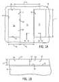
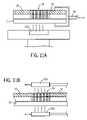
- FIG. 1Aillustrates a diagrammatic top plan view of a portion of a substrate at a preliminary processing stage according to an embodiment of the present disclosure, showing the substrate with trenches.
- FIGS. 1B-1Care elevational, cross-sectional views of embodiments of the substrate depicted in FIG. 1A taken along lines 1 B/ 1 C- 1 B/ 1 C.
- FIG. 1Dis an elevational, cross-sectional view of a substrate used in another embodiment of the invention.
- FIGS. 2A-6Aillustrate diagrammatic top plan views of the substrate of FIG. 1A at various stages of the fabrication of a self-assembled block copolymer film according to an embodiment of the present disclosure.
- FIGS. 2B to 6B and 2 C to 6 Cillustrate elevational, cross-sectional views of embodiments of a portion of the substrate depicted in FIGS. 2A-6A taken, respectively, along lines 2 B/ 2 C- 2 B/ 2 C to lines 6 B/ 6 C- 6 B/ 6 C.
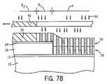
- FIGS. 7A-7Billustrate elevational, cross-sectional views of the substrate depicted in FIG. 5B , showing annealing of a portion of the film at various stages according to an embodiment of the disclosure by use of a laser source illuminated through a mask or reticle.
- FIG. 8Aillustrates a diagrammatic top plan view of the substrate of FIG. 1A , showing the incorporation of thermally conductive lines in the substrate for localized heating of the film layer according to an embodiment of the disclosure.
- FIG. 8Billustrates an elevational, cross-sectional view of the substrate depicted in FIG. 8A taken along lines 8 B- 8 B.
- FIG. 9illustrates an elevational, cross-sectional view of the substrate of FIG. 1A , showing the incorporation of an absorptive material layer for localized heating of the film layer according to another embodiment of the disclosure.
- FIG. 10Aillustrates a diagrammatic top plan view of the substrate of FIG. 1A , showing the incorporation of a reflective material layer on the exposed surfaces outside of the trenches for localized heating of the film layer according to another embodiment of the disclosure.
- FIG. 10Bis an elevational, cross-sectional view of the substrate depicted in FIG. 10A taken along lines 10 B- 10 B.
- FIGS. 11A-11Billustrate embodiments of heating the substrate of FIG. 5B by zoned annealing techniques.
- FIG. 12 Aillustrates a diagrammatic top plan view of a portion of the substrate of FIG. 6A at a subsequent stage.
- FIGS. 12B and 12Dillustrate elevational, cross-sectional views of the substrate depicted in FIG. 12A taken along lines 12 B/ 12 D- 12 B/ 12 D.
- FIG. 12Cillustrates an intermediate structure showing the removal of half-cylindrical domains in a step prior to FIG. 12D .
- semiconductor substrateor “semiconductive substrate” or “semiconductive wafer fragment” or “wafer fragment” or “wafer” will be understood to mean any construction comprising semiconductor material, including but not limited to bulk semiconductive materials such as a semiconductor wafer (either alone or in assemblies comprising other materials thereon), and semiconductive material layers (either alone or in assemblies comprising other materials).
- substraterefers to any supporting structure including, but not limited to, the semiconductive substrates, wafer fragments or wafers described above.
- “L o ”is the inherent pitch (bulk period or repeat unit) of structures that self assemble upon annealing from a self-assembling (SA) block copolymer or a blend of a block copolymer with one or more of its constituent homopolymers.
- SAself-assembling
- Processing conditions of embodiments of the inventionuse a graphoepitaxy technique utilizing the sidewalls of trenches as constraints to induce orientation and registration of a first film of a self assembling diblock copolymer to form an ordered linear array pattern registered to the trench sidewalls.
- the first polymer filmis then used as a template or base layer for inducing the ordering of a subsequently deposited lamellar-phase block copolymer film such that, upon annealing, the lamellar domains within the trenches orient perpendicularly and are registered to the underlying structures, resulting in a stacked double- or multi-layer structure having a striped pattern.
- FIGS. 1A-11DSteps in a method for fabricating thin films from self assembling (SA) block copolymers that define nanometer-scale linear array patterns according to embodiments of the invention are illustrated in FIGS. 1A-11D .
- SAself assembling
- the methodfirst forms a multi-layer pattern within trenches by forming a polymer base film or template with ordered structures within the trenches for inducing the ordering of an overlying lamellar phase block copolymer film such that the lamellar domains are oriented perpendicularly and registered to the underlying assembled domains of the base film.
- the base layer within the trenchescan be formed from a lamellar-phase block copolymer film, which upon annealing forms a registered lamellar array of alternating polymer-rich blocks that extend the length and are oriented parallel to the sidewalls and perpendicular to the floor of the trenches.
- the base layeris formed from a cylindrical-phase block copolymer material which, upon annealing, forms lines of half-cylinders in a polymer matrix extending the length and oriented parallel to the sidewalls and floor of the trenches.
- the assembled base filmis then used as a template for inducing the ordering of an overlying lamellar-phase block copolymer film such that the lamellar domains of the annealed film are oriented perpendicularly and registered to the underlying pattern of the base film within the trenches.
- the surface of the sidewalls and edges of the trenchesare preferential wetting by one block of the copolymer and the trench floors are neutral wetting (equal affinity for both blocks of the copolymer) to allow both blocks of the copolymer material to wet the floor of the trench.
- Entropic forcesdrive the wetting of a neutral wetting surface by both blocks, resulting in the formation of a layer of perpendicular lamellae across the width of each trench.
- a substrate 10is provided bearing a neutral wetting surface.
- the substrate 10can comprise, for example, silicon (with native oxide), oxide (e.g., silicon oxide, SiO x ), or an inorganic film.
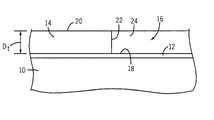
- a neutral wetting layer 12is formed on the substrate 10 prior to forming the overlying material layer 14 (e.g., oxide). Etching through the material layer 14 to form the trenches 16 exposes the underlying neutral wetting layer 12 as the floor or bottom surface 18 of the trench.
- the trenchesare separated by a spacer or crest 20 having a width (w s ) and are structured with opposing sidewalls 22 , opposing ends or edges 24 , a width (w t ), a length (I t ) and a depth (D t ).
- a neutral wetting surfacecan be provided, for example, by applying a neutral wetting polymer to form a layer 12 on the surface of the substrate 10 .
- a neutral wetting polymerfor example, by applying a neutral wetting polymer to form a layer 12 on the surface of the substrate 10 .
- SAself-assembling
- PS-r-PMMArandom PS:PMMA copolymer brush layer
- the brushcan be affixed by grafting (on an oxide substrate) or by cross-linking (any surface) using UV radiation or thermal processing.
- a random copolymer solution composed of PS and PMMA with hydroxyl end group(s)can be applied to the surface of the substrate 10 as a layer about 5-10 nm thick and end-grafted by heating at about 160° C. for about 48 hours.
- a surface that is neutral wetting to PS-b-PMMAcan be prepared by spin coating a blanket layer of a photo- or thermally cross-linkable random copolymer such as a benzocyclobutene- or azidomethylstyrene-functionalized random copolymer of styrene and methyl methacrylate (e.g., poly(styrene-r-benzocyclobutene-r-methyl methacrylate (PS-r-PMMA-r-BCB) onto the surface of the substrate 10 prior to forming the material layer 14 .
- a photo- or thermally cross-linkable random copolymersuch as a benzocyclobutene- or azidomethylstyrene-functionalized random copolymer of styrene and methyl methacrylate (e.g., poly(styrene-r-benzocyclobutene-r-methyl methacrylate (PS-r-PMMA-r-BCB) onto
- such a random copolymercan comprise about 42% PMMA, about (58-x)% PS and x % (e.g., about 2-3%) of either polybenzocyclobutene or poly(para-azidomethylstyrene)).
- An azidomethylstyrene-functionalized random copolymercan be UV crosslinked (e.g., 1-5 mW/cm ⁇ 2 exposure for about 15 seconds to about 30 minutes) or thermally crosslinked (e.g., at about 170° C.).
- a benzocyclobutene-functionalized random copolymercan be thermally cross-linked (e.g., at about 200° C. for about 4 hours or at about 250° C. for about 10 minutes).
- Another neutral wetting surface for PS-b-PMMAcan be provided by hydrogen-terminated silicon, which can be prepared by a conventional process, for example, by a fluoride ion etch of a silicon substrate 10 (with native oxide present, about 12-15 ⁇ ) for example, by immersion in aqueous solution of hydrogen fluoride (HF) and buffered HF or ammonium fluoride (NH 4 F), by HF vapor treatment, by exposure to hot H 2 vapor, or by a hydrogen plasma treatment (e.g., atomic hydrogen).
- HFhydrogen fluoride
- NH 4 Fbuffered HF or ammonium fluoride
- the material layer 14can be formed on the substrate 10 and etched to form the trenches 16 , and a neutral wetting material 12 then applied to the trench floors 18 .
- trench floors that are neutral wetting to PS-b-PMMAcan be prepared by spin coating PS-r-PMMA-r-BCB onto the surface of the substrate 10 within the trenches and thermally crosslinking the polymer (e.g., 190° C., 4 hours) to form a crosslinked polymer mat as a neutral wetting layer 12 . Capillary forces pull the random copolymer to the bottom of deep trenches. Non-crosslinked polymer material can be subsequently removed.
- the trench sidewalls 22are preferential wetting by one block of the copolymer to induce formation of lamellae as the blocks self-assemble.
- the material layer 14 defining the trench surfacescan be an inherently preferential wetting material, or in other embodiments, a layer of a preferential wetting material can be applied onto the surfaces of the trenches.
- an oxidee.g., silicon oxide, SiO x
- a clean silicon surfacewith native silicon oxide
- a thin (e.g., 1 ⁇ 4 pitch) interface layer of PMMA and alternating PMMA and PS lamellaee.g., 1 ⁇ 2 pitch
- PMMApolymethylmethacrylate
- a PMMA that is modified with a moiety containing one or more hydroxyl (—OH) groupscan be applied by spin coating and then heated (e.g., to about 170° C.) to allow the OH groups to end-graft to the oxide sidewalls 22 and ends 24 of the trenches.
- Non-grafted materialcan be removed from the neutral wetting layer 12 by rinsing with an appropriate solvent (e.g., toluene).
- an appropriate solvente.g., toluene
- toluenee.g., toluene
- the surfaces of the floor 18 ′, sidewalls 22 ′ and the ends 24 ′ of the trenches 16 ′are preferential wetting by the minority block of the copolymer to induce formation of parallel lines of half-cylinders wetting the air interface (surface exposed) down the middle of each trench aligned parallel to the trench sidewalls and floor.
- substrate 10 ′can be composed of an inherently preferential wetting material such as a clean silicon surface (with native silicon oxide) and material layer 14 ′ can be composed of oxide (e.g., SiO x ).
- Both materialsexhibit preferential wetting toward the PMMA block to result in the assembly of a thin interface layer of PMMA on the trench sidewalls as well as PMMA cylinders in the center of a PS matrix within each trench.
- Other preferential wetting surfaces to PMMAcan be provided, for example, by silicon nitride, silicon oxycarbide, and PMMA polymer grafted to a sidewall material such as silicon oxide, and resist materials such as such as methacrylate-based resists. See, for example, C. T. Black and O. Bezencenet, “Nanometer-Scale Pattern Registration and Alignment by Directed Diblock Copolymer Self-Assembly,” IEEE Transactions on Nanotechnology, 2004, 3(3), 412-415; C. T.
- the trench sidewalls, edges and floorsinfluence the structuring of the array of nanostructures within the trenches.
- the boundary conditions of the trench sidewalls in both the x- and y-axisimpose a structure wherein each trench contains n number of features (i.e., cylinders or lamellae).
- Factors in forming a single array or layer of nanostructures within the trenchesinclude the width and depth of the trench, the formulation of the block copolymer to achieve the desired pitch (L o ), and the thickness (t) of the copolymer film.
- the trenches 16are constructed with a width (w t ) such that a block copolymer (or blend) will self assemble upon annealing into a single layer of “n” structures spanning the width (w t ) of the trench, with each structure (i.e., cylinders or lamellae) being separated by a value of L o (from center-to-center).
- the width (w t ) of the trenchesis a multiple of the inherent pitch value (L o ) of the polymer being equal to or about nL o (“n*L o ”), typically ranging from about n*10 to about n*100 nm (with n being the number of features or structures).
- the depth (D t ) of the trenchesis greater than or at about L o in using a lamellar-phase block copolymer for the base layer ( FIGS. 1B-1C ), and less than L o in using a cylindrical-phase block copolymer ( FIG. 1D ).
- the application and annealing of a block copolymer material having an inherent pitch value of L o in a trench having a width (w t ) at or about L owill result in the formation of a single layer of “n” structures spanning the width and registered to the sidewalls for the length of the trench.
- the trench dimensionis about 50-500 nm wide (w t ) and about 1,000-10,000 ⁇ m in length (I t ), with a depth (D t ) of about 50-500 nm in using a lamellar-forming block copolymer, and about 50-2000 nm wide (w t ) with a depth (D t ) of about 15-25 nm in using a cylinder-forming block copolymer.
- the width (w s ) of the spacer or crest 20 between adjacent trenchesis at or about an integral multiple of L o such that as the film situated on the crest is annealed, the expanding registered fronts will be matched and aligned where they converge.
- the spacer width (w s )can vary from about the width (w t ) of the trench 16 to up to about 10-20 ⁇ the trench width.
- the trenchescan be formed using a lithographic tool having an exposure system capable of patterning at the scale of L o (10-100 nm).
- exposure systemsinclude, for example, extreme ultraviolet (EUV) lithography, proximity X-rays, and electron beam (e-beam) lithography, as known and used in the art.
- EUVextreme ultraviolet
- e-beamelectron beam
- Conventional photolithographycan attain (at smallest) about 58 nm features.
- a self-assembling (SA) block copolymer material 26 having an inherent pitch at or about L o (or a ternary blend of block copolymer and homopolymers blended to have a pitch at or about L o )is then deposited, typically by spin casting (spin-coating), onto the floor 18 of the trenches.
- the block copolymer materialcan be deposited onto the patterned surface by spin casting from a dilute solution (e.g., about 0.25-2 wt % solution) of the copolymer in an organic solvent such as dichloroethane (CH 2 Cl 2 ) or toluene, for example.
- a layer of the first block copolymer material 26is deposited into the trenches 16 to a thickness (t l ) less than the trench depth (D t ), for example, at about one-half of the trench depth, and at or about the L o value of the block copolymer material such that the copolymer film layer will self assemble upon annealing to form a single layer of lamellae across the width (w t ) of the trench.
- a layer of the first block copolymer material 26is deposited into the trenches 16 to a thickness (t l ) greater than the trench depth (D t ) but less than L o such that the copolymer film layer will self assemble upon annealing to form a single layer of parallel lines of half-cylinders across the width (w t ) of the trench.
- a typical thickness (t l ) of a lamellar-phase block copolymer film 26is about ⁇ 20% of the L o value of the polymer (e.g., about 10-100 nm) to form, for example, alternating polymer-rich lamellar blocks having a width of about L o (e.g., 25-35 nm).
- the thickness (t l ) of a cylindrical-phase block copolymer film 26is less than L o to form parallel-oriented half-cylinders of one block having a diameter of about L o in a matrix of another block within each trench.
- the thickness of the filmcan be measured, for example, by ellipsometry techniques.
- diblock copolymersare used in the illustrative embodiment, other types of block copolymers (i.e., triblock or triblock or multiblock copolymers) can be used.
- diblock copolymersinclude poly(styrene-block-methyl methacrylate) (PS-b-PMMA), polyethyleneoxide-polyisoprene, polyethyleneoxide-polybutadiene, polyethyleleoxide-polystyrene, polyetheleneoxide-polymethylmethacrylate, polystyrene-polyvinylpyridine, polystyrene-polyisoprene (PS-b-PI), polystyrene-polybutadiene, polybutadiene-polyvinylpyridine, and polyisoprene-polymethylmethacrylate, among others.
- PS-b-PMMApoly(styrene-block-methyl methacrylate)
- PS-b-PMMApoly
- triblock copolymersexamples include poly(styrene-block methyl methacrylate-block-ethylene oxide).
- One of the polymer blocks of the block copolymershould be selectively and readily removable in order to fabricate an etch mask or template from the annealed film.
- the volume fractions of the two blocks (AB)are generally at a ratio between about 50:50 and 60:40.
- An example of a lamellae-forming symmetric diblock copolymeris PS-b-PMMA with a weight ratio of about 50:50 (PS:PMMA) and total molecular weight (M n ) of about 51 kg/mol.
- the volume fractions of the two blocks (AB)are generally at a ratio between about 60:40 and 80:20.
- the Chi value of the polymer blocks (e.g., PS and PMMA) at common annealing temperaturesis generally small such that the air interface is equally or non-selectively wetting to both blocks.
- the block copolymer materialcan also be formulated as a binary or ternary blend comprising a SA block copolymer and one or more homopolymers of the same type of polymers as the polymer blocks in the block copolymer, to produce blends that swell the size of the polymer domains and increase the L o value of the polymer.
- the volume fraction of the homopolymerscan range from 0 to about 40%.
- An example of a ternary diblock copolymer blendis a PS-b-PMMA/PS/PMMA blend, for example, 46K/21K PS-b-PMMA containing 40% 20K polystyrene and 20K poly(methylmethacrylate).
- the L o value of the polymercan also be modified by adjusting the molecular weight of the block copolymer, e.g., for lamellae, L o ⁇ (MW) 2/3 .
- ellipticitycan be induced in the structures by creating a slight mismatch between the trench and the spacer widths and the inherent pitch (L o ) of the block copolymer or ternary blend, as described, for example, by Cheng et al., “Self-assembled One-Dimensional Nanostructure Arrays,” Nano Lett., 2006, 6(9), 2099-2103, the disclosure of which are incorporated by reference herein, which then reduces the stresses that result from such mismatches.
- the first block copolymer film 26is then annealed, for example, by thermal annealing to above the glass transition temperature of the component blocks of the copolymer material to cause the polymer blocks to separate and self assemble according to the preferential and neutral wetting of the trench surfaces 16 , 18 , 22 , to form a self-assembled block copolymer structure 28 .
- a PS-b-PMMA copolymer filmcan be annealed at a temperature of about 180-195° C. in a vacuum oven for about 1-24 hours to achieve the self-assembled morphology.
- the filmcan also be solvent annealed, for example, by slowly swelling both blocks of the film with a solvent, then slowly evaporating the solvent.
- the constraints provided by the width (w t ) of the trenches and the character of the copolymer composition combined with preferential or neutral wetting surfaces within the trenchesresults, upon annealing, in a single layer of n elements across the width (w t ) of the trench.
- the number “n” or pitches of elements (e.g., lamellar blocks or half-cylinders) within a trenchis according to the width (w t ) of the trench and the molecular weight (MW) of the block copolymer.
- a lamellar-phase block copolymer material used to form the base layer 28will, upon annealing, self assemble into perpendicular-oriented, alternating polymer-rich blocks 30 , 32 spanning the width (w t ) of the trench 16 at an average pitch value at or about L o .
- annealing of a cylindrical-phase copolymer material to form the base layer 28 ′will result in parallel-oriented half-cylinders 30 ′ within a polymer matrix 32 ′ spanning the width (w t ) of the trench 16 ′, with each cylinder being separated by an average value of at or about L o , and an interface layer 30 a ′ along the sidewalls 22 ′ and floor 18 ′.
- the resulting morphologies of the annealed base film 28can be examined, for example, using atomic force microscopy (AFM), transmission electron microscopy (TEM), or scanning electron microscopy (SEM).
- AFMatomic force microscopy
- TEMtransmission electron microscopy
- SEMscanning electron microscopy
- the annealed and ordered base film 28is then treated to crosslink the polymer segments to fix and enhance the strength of the self-assembled polymer blocks 30 , 32 within the trenches 16 (e.g., to crosslink the PS segments).
- the polymerscan be structured to inherently crosslink (e.g., upon UV exposure), or one or both of the polymer blocks of the copolymer material can be formulated to contain a crosslinking agent.
- the trench regionscan selectively exposed through a reticle to crosslink only the self-assembled film 28 within the trenches 16 .
- a washcan then be applied with an appropriate solvent such as toluene, to remove the non-crosslinked portions of the film 28 (e.g., on the spacer or crest 20 ) leaving the registered self-assembled base film within the trenches and exposing the surface of material layer 14 above/outside the trenches (e.g., the crest 20 ).
- an appropriate solventsuch as toluene
- a neutral wetting layer 34can then be formed on the exposed surface of the material layer 14 (e.g., oxide), for example by applying and grafting or crosslinking a random copolymer brush layer (e.g., PS-r-PMMA) on the surface.
- the material layer 14e.g., oxide
- a random copolymer brush layere.g., PS-r-PMMA
- the entire annealed film 28can be crosslinked globally.
- a photoresist layercan be applied to pattern and expose the areas of the film outside the trench regions (e.g., over the crests 20 ), and the exposed portions of the film can be removed, for example by an oxygen (O 2 ) plasma treatment. The photoresist can then be removed (e.g., stripped).
- a neutral wetting filmcan then be formed on the exposed portions of the material layer 14 above the trench regions (e.g., the crests 20 ).
- a film of a photo-crosslinkable, neutral wetting random copolymercan be globally applied (e.g., cast) and photoexposed through a reticle to selectively crosslink the neutral wetting film only over the portions of the material layer 14 above the trenches (e.g., the crests).
- Non-grafted or non-crosslinked portions of the neutral wetting filmcan then be removed, for example, by a solvent rinse (e.g., toluene).
- a solvent rinsee.g., toluene
- a layer of a lamellar-phase block copolymer material 36 having an inherent pitch at or about L ois then deposited (e.g., by spin casting) onto the annealed and crosslinked base film 28 within the trenches and onto the neutral wetting layer 34 overlying the material layer 14 (e.g., crest 20 ) outside the trenches 16 .
- the copolymer materialcan be spin cast, for example, from a dilute solution of the copolymer in an organic solvent (e.g., about 0.25-2 wt % solution).
- the lamellar-phase block copolymer layer 36is cast over the neutral wetting layer 34 (e.g., over crest 20 ) and the base film 28 within the trenches to a thickness (t 2 ) at or about the L o value of the block copolymer material 36 such that, upon annealing, the copolymer film layer will self-assemble to form a single layer of perpendicular-oriented lamellar domains each having a width (w 2 ) of about L o .
- annealing of the lamellar-phase block copolymer layer 36is then conducted to cause the polymer blocks to separate and self assemble into a film 38 composed of perpendicular-oriented lamellar-phase domains 40 , 42 in a striped pattern, for example, at about 180-195° C. for a PS-b-PMMA copolymer film.
- An annealing processis performed to achieve ordering of the lamellar blocks across plateaus or crests 20 between the trenches 16 and other areas of the substrate that are without constraints or defined features or boundaries (e.g., trench sidewalls and/or edges) to which self-assembling copolymer blocks can align.
- embodiments of the inventionutilize techniques for performing an anneal of the copolymer film by a localized application of thermal energy to portions of the polymer film that have registry to them.
- a limited area of the lamellar-forming film 36 over and above the trenches 16is selectively heated to cause self-assembly of the polymer domains and produce ordered lamellar domains that are registered to the underlying base film 28 within the trenches.
- the base film 28imposes an induced ordering effect on the overlying self-assembling lamellar film 36 to reproduce the underlying pattern of the base film.
- Intrinsic periods of the two block copolymer materials 26 , 36can be matched, for example, through a ternary blend of either or both of the copolymer materials with one or more homopolymers to adjust the polymer periods (L o values). See, for example, R. Ruiz, R. L. Sandstrom and C. T. Black, “Induced Orientational Order in Symmetric Diblock Copolymer Thin-Films,” Advanced Materials, 2007, 19(4), 587-59, the disclosure of which is incorporated by reference herein.
- this initial annealresults in the formation of a single layer 38 of assembled and ordered, perpendicular-oriented lamellar domains 40 , 42 that are registered to the underlying assembled domains of the base film 28 within the trenches 16 , i.e., the lamellar domains 30 , 32 ( FIG. 5B ) or the half-cylinders 30 ′ and matrix domains 32 ′ ( FIG. 5C ) of the base film within the trenches.
- the annealed copolymer layer 38comprises alternating stripes of the two components of the lamellar-phase block copolymer.
- a temperature gradientcan be provided across the substrate, with the temperature above the glass transition temperature in regions where annealing of the film occurs to produce registered and ordered structures, and below the glass transition temperature in areas outside of those regions.
- the zone of thermal heating(“thermal corona”) is expanded laterally, using the initially formed self-assembled lamellar structure 38 over the trenches 16 to induce an ordering effect on the adjacently situated unannealed portion of the polymer film 36 beyond the edges of the trenches (region “B 1 ”).
- the localized heating of the lamellar-forming film 36is performed to limit heating to about 3-4 to 6-8 pitches or repeat units, L o , of the copolymer film 30 at a time, e.g., to dashed line “B 1 ” in FIGS. 5A-5C .
- the newly annealed portion of the filmi.e., region “B 1 ” will then self-assemble into perpendicular-oriented lamellar domains in an ordered repeat pattern that matches and is registered to the previously formed adjacent array within region “A”, as shown in FIGS. 6A-6C .
- the zone of heatingcan be further expanded laterally (region “B 2 ”) to anneal additional portions of the second block copolymer film adjacent to the previously annealed and ordered portion of the film (i.e., region “B 1 ”) to extend the range of ordered structures over the substrate until the desired pattern repeat structure is obtained.
- annealing of the lamellar-phase block copolymer layer 36is accomplished by focused and localized thermal heating of a targeted area (e.g., region “A”) by directing a laser source 44 of short-UV wavelength onto the film.
- the laser source 44(with adequate power) can be illuminated through a mask (or reticle) 46 or masking elements associated with a laser beam apparatus that shades all areas except for the trenches or inner portions of the trenches ( FIG. 7A ).
- the sections of the film situated above the ordered cylindrical film within the trencheswill self-assemble first and in registry with the pattern of the underlying base film 28 .
- the continued addition of thermal energy radiating laterally from the initially assembled, registered portion of the film 36can be applied to result in regular, registered self assembly across the breadth of the lamellar-phase film 36 (regions “B 1 ” as in FIG. 5A ).
- the laser beam 44can also be expanded (e.g., defocused) to widen the area of coverage of the film 36 , or step-scanned or sweep-scanned across the substrate (arrow ⁇ in FIG. 7B ), with the scanning rate set appropriately.
- the laser sourceis applied at appropriate parameters (e.g., wavelength, pulse length, intensity) to anneal the targeted area of the film 36 .
- the annealcan be provided using a pulsed laser source.
- a series of thin lines 48 of a thermally conductive materialcan be formed in or on the substrate 10 prior to forming the material layer 14 .
- the conductive lines 48are provided to extend beneath the trenches 16 , and optionally to extend under the material layer 14 beyond the trenches. Heat can be generated through the conductive lines 48 to initially anneal the film 36 above the trenches (within region “A”), and then to radiate laterally to anneal areas of the film adjacent to the self-assembled film 38 above the trenches (region “B 1 ”).
- selective localized heating of the lamellar-phase film 36can be provided by selectively applying an absorptive material layer 50 to substrate 10 prior to depositing the neutral wetting layer 12 and the material layer 14 , as shown in the embodiment depicted in FIG. 9 , or a reflective material layer 50 ′ to the surface of the material layer 14 ′ outside of the trenches (e.g., the crests 20 ′) as depicted in FIGS. 10A-10B .
- a radiative heat sourcee.g., infrared (ir) heat source or quartz lamp
- a radiative heat sourcee.g., infrared (ir) heat source or quartz lamp
- the power of the light sourcecan then be slowly increased to expand the area having a temperature above the glass transition temperature, allowing the ordered formation of lamellae along the advancing hot zone.
- suitable materials for layer 50FIG.
- absorptive materialssuch as silicon carbide and organic infrared (IR) or near-infrared (NIR) absorbers such as Lumogen® fluorescent dyes (e.g., Lumogen IR 765® and Lumogen IR 788®) (BASF), among others.
- IRorganic infrared
- NIRnear-infrared
- the neutral wetting layer 12can be modified or tailored with absorptive functionality.
- suitable materials for layer 50 ′FIGS. 10A-10B
- reflective metalssuch as aluminum (Al), tungsten (W), chromium (Cr), copper (Cu), ruthenium (Ru), nickel (Ni), among others.
- the backside of the substratee.g., wafer
- the backside of the substratecan be heated (arrows ⁇ ) to produce differences in emissivity between the trench bottom (floor) 18 and the surrounding areas to yield a desired temperature gradient.
- a coating 50 of a low emissivity materiale.g., a metal such as aluminum, tungsten, etc.
- a low emissivity materialcan be applied to the trench floors 18 which will radiate less heat and maintain a higher temperature than the surrounding area.
- the film 36can be annealed in a moving temperature gradient (zone annealed).
- the film 36can be moved across a hot-cold temperature gradient 52 a positioned above the film or beneath the substrate 10 (as shown) at a translational set speed (e.g., about 0.05-10 ⁇ m/second) using a motorized translation stage 54 whereupon ordering of nanostructures occurs at the backside as the film re-cools after passing under or over the heat source.
- a heat sourcecan be positioned above the film 36 (e.g., 52 b ) and/or or beneath the substrate 10 (e.g., 52 b ′) and moved across the film using a motorized mechanism.
- one of the block componentscan be selectively removed to produce a thin film 56 that can be used, for example, as a lithographic template or mask to pattern the underlying substrate 10 (and material layer 14 on the crests 20 ) in a semiconductor processing to define regular patterns in the nanometer size range (i.e., about 10-100 nm).
- a lamellar domaine.g., 40
- the underlying polymer domain of the base filme.g., 30
- Removal of the PMMA phase domains 30 , 40can be performed, for example, by application of an oxygen (O 2 ) plasma, or by a chemical dissolution process such as acetic acid sonication by first irradiating the sample (ultraviolet (UV) radiation, 1 J/cm ⁇ 2 254 nm light), then ultrasonicating the film in glacial acetic acid, ultrasonicating in deionized water, and rinsing the film in deionized water to remove the degraded PMMA.
- O 2oxygen
- acetic acid sonicationby first irradiating the sample (ultraviolet (UV) radiation, 1 J/cm ⁇ 2 254 nm light), then ultrasonicating the film in glacial acetic acid, ultrasonicating in deionized water, and rinsing the film in deionized water to remove the degraded PMMA.
- the PS matrix 32 ′ situated underneath the half-cylinders 30 ′ and over the trench floors 18 ′remains after the removal of the PMMA domains, and is removed, for example, by plasma O 2 etch, prior to a patterning process to expose the underlying substrate 10 as illustrated in FIG. 12D .
- the selective removal of PS phase domains 32 , 42will result in openings (slits) separated by PMMA lamellar domains 30 , 40 .
- the resulting filmshave a corrugated surface that defines a linear pattern of fine, nanometer-scale, parallel slits (openings) 58 about 5-50 nm wide and several microns in length (e.g., about 10-4000 ⁇ m), the individual slits separated by a polymer matrix 42 about 5-50 nm wide.
- openingsfine, nanometer-scale, parallel slits (openings) 58 about 5-50 nm wide and several microns in length (e.g., about 10-4000 ⁇ m)
- the individual slits separated by a polymer matrix 42about 5-50 nm wide.
- removal of the PMMA domainsaffords a PS mask of sublithographic dimensions, for example, a pitch of about 35 nm (17.5 nm PS domain). A smaller pitch can be dialed in by using lower molecular weight diblock copolymers.
- the filmscan be used, for example, as a lithographic template or etch mask to pattern (arrows ⁇ ) the underlying substrate 10 (and layer 14 ), for example, by a non-selective RIE etching process, to delineate a series of channels or grooves 60 , shown in phantom in FIG. 11B .
- the channelscan then be filled with a conductive material (e.g., metal) to form nanowire channel arrays for transistor channels, semiconductor capacitors, and other structures, or with a dielectric material to separate active areas. Further processing can then be performed as desired.
- a conductive materiale.g., metal
- the filmsprovide linear arrays having long range ordering and registration for a wide field of coverage for templating a substrate.
- the filmsare useful as etch masks for producing close pitched nanoscale channel and grooves that are several microns in length, for producing features such as floating gates for NAND flash with nanoscale dimensions.
- photolithography techniquesare unable to produce channels much below 60 nm wide without high expense. Resolution can exceed other techniques such as conventional photolithography, while fabrication costs utilizing methods of the disclosure are far less than electron beam (E-beam) or EUV photolithographies which have comparable resolution.
Landscapes
- Engineering & Computer Science (AREA)
- Chemical & Material Sciences (AREA)
- Nanotechnology (AREA)
- Manufacturing & Machinery (AREA)
- Physics & Mathematics (AREA)
- Crystallography & Structural Chemistry (AREA)
- Microelectronics & Electronic Packaging (AREA)
- General Physics & Mathematics (AREA)
- Condensed Matter Physics & Semiconductors (AREA)
- Medicinal Chemistry (AREA)
- Materials Engineering (AREA)
- Polymers & Plastics (AREA)
- Chemical Kinetics & Catalysis (AREA)
- Health & Medical Sciences (AREA)
- Analytical Chemistry (AREA)
- Composite Materials (AREA)
- Organic Chemistry (AREA)
- Mathematical Physics (AREA)
- Theoretical Computer Science (AREA)
- Computer Hardware Design (AREA)
- Treatments Of Macromolecular Shaped Articles (AREA)
- Exposure Of Semiconductors, Excluding Electron Or Ion Beam Exposure (AREA)
- Photosensitive Polymer And Photoresist Processing (AREA)
- Moulding By Coating Moulds (AREA)
- Laminated Bodies (AREA)
Abstract
Description
- Embodiments of the invention relate to methods of fabricating nanoscale linear arrays of microstructures and microchannels by use of thin films of self-assembling block copolymers, and devices resulting from those methods.
- As the development of nanoscale mechanical, electrical, chemical and biological devices and systems increases, new processes and materials are needed to fabricate nanoscale devices and components. Conventional optical lithographic processing methods are not able to accommodate fabrication of structures and features much below the 100 nm level. The use of self assembling diblock copolymers presents another route to patterning at nanometer dimensions. Diblock copolymer films spontaneously assembly into periodic structures by microphase separation of the constituent polymer blocks after annealing, for example by thermal annealing above the glass transition temperature of the polymer or by solvent annealing, forming ordered domains at nanometer-scale dimensions. Following self assembly, one block of the copolymer can be selectively removed and the remaining patterned film used as an etch mask for patterning nanosized features into the underlying substrate. Since the domain sizes and periods (Lo) involved in this method are determined by the chain length of a block copolymer (MW), resolution can exceed other techniques such as conventional photolithography, while the cost of the technique is far less than electron beam lithography or EUV photolithography which have comparable resolution.
- The film morphology, including the size and shape of the microphase-separated domains, can be controlled by the molecular weight and volume fraction of the AB blocks of a diblock copolymer to produce lamellar, cylindrical, or spherical morphologies, among others. For example, for volume fractions at ratios greater than about 80:20 of the two blocks (AB) of a diblock polymer, a block copolymer film will microphase separate and self-assemble into a periodic spherical domains with spheres of polymer B surrounded by a matrix of polymer A. For ratios of the two blocks between about 60:40 and 80:20, the diblock copolymer assembles into a periodic hexagonal close-packed or honeycomb array of cylinders of polymer B within a matrix of polymer A. For ratios between about 50:50 and 60:40, lamellar domains or alternating stripes of the blocks are formed. Domain size typically ranges from 5-50 nm.
- Diblock copolymer thin films of cylindrical and lamellar phases may both form striped phases relative to an interface. For cylindrical phase films, a striped pattern results from parallel cylinder orientation, while for lamellar phase films, a striped pattern results from perpendicular domain orientation. From a top down view, perpendicular-oriented lamellae and parallel-oriented cylinders appear similar, e.g., as parallel lines.
- Graphoepitaxy techniques using defined topography such as trench edges have been used in an attempt to orient and order copolymer domains and control registration and alignment of the self-assembled blocks to form a desired pattern. By comparison, thin films prepared on a flat substrate and annealed do not have any preferential orientation of domains and will assemble into a disordered fingerprint-like structure despite extensive annealing. Although registered and ordered arrays of cylinders have been produced within trenches, the fabrication of an ordered array of repeat structures outside of the confines of trenches and over large areas has not been realized in a manufacturable process.
- It would be useful to provide a method of fabricating films of linear arrays of ordered nanostructures that overcome these problems.
- Embodiments of the invention are described below with reference to the following accompanying drawings, which are for illustrative purposes only. Throughout the following views, the reference numerals will be used in the drawings, and the same reference numerals will be used throughout the several views and in the description to indicate same or like parts.
FIG. 1A illustrates a diagrammatic top plan view of a portion of a substrate at a preliminary processing stage according to an embodiment of the present disclosure, showing the substrate with trenches.FIGS. 1B-1C are elevational, cross-sectional views of embodiments of the substrate depicted inFIG. 1A taken alonglines 1B/1C-1B/1C.FIG. 1D is an elevational, cross-sectional view of a substrate used in another embodiment of the invention.FIGS. 2A-6A illustrate diagrammatic top plan views of the substrate ofFIG. 1A at various stages of the fabrication of a self-assembled block copolymer film according to an embodiment of the present disclosure.FIGS. 2B to 6B and2C to6C illustrate elevational, cross-sectional views of embodiments of a portion of the substrate depicted inFIGS. 2A-6A taken, respectively, alonglines 2B/2C-2B/2C tolines 6B/6C-6B/6C.FIGS. 7A-7B illustrate elevational, cross-sectional views of the substrate depicted inFIG. 5B , showing annealing of a portion of the film at various stages according to an embodiment of the disclosure by use of a laser source illuminated through a mask or reticle.FIG. 8A illustrates a diagrammatic top plan view of the substrate ofFIG. 1A , showing the incorporation of thermally conductive lines in the substrate for localized heating of the film layer according to an embodiment of the disclosure.FIG. 8B illustrates an elevational, cross-sectional view of the substrate depicted inFIG. 8A taken alonglines 8B-8B.FIG. 9 illustrates an elevational, cross-sectional view of the substrate ofFIG. 1A , showing the incorporation of an absorptive material layer for localized heating of the film layer according to another embodiment of the disclosure.FIG. 10A illustrates a diagrammatic top plan view of the substrate ofFIG. 1A , showing the incorporation of a reflective material layer on the exposed surfaces outside of the trenches for localized heating of the film layer according to another embodiment of the disclosure.FIG. 10B is an elevational, cross-sectional view of the substrate depicted inFIG. 10A taken alonglines 10B-10B.FIGS. 11A-11B illustrate embodiments of heating the substrate ofFIG. 5B by zoned annealing techniques.- FIG.12A—illustrates a diagrammatic top plan view of a portion of the substrate of
FIG. 6A at a subsequent stage.FIGS. 12B and 12D illustrate elevational, cross-sectional views of the substrate depicted inFIG. 12A taken alonglines 12B/12D-12B/12D.FIG. 12C illustrates an intermediate structure showing the removal of half-cylindrical domains in a step prior toFIG. 12D . - The following description with reference to the drawings provides illustrative examples of devices and methods according to embodiments of the invention. Such description is for illustrative purposes only and not for purposes of limiting the same.
- In the context of the current application, the term “semiconductor substrate” or “semiconductive substrate” or “semiconductive wafer fragment” or “wafer fragment” or “wafer” will be understood to mean any construction comprising semiconductor material, including but not limited to bulk semiconductive materials such as a semiconductor wafer (either alone or in assemblies comprising other materials thereon), and semiconductive material layers (either alone or in assemblies comprising other materials). The term “substrate” refers to any supporting structure including, but not limited to, the semiconductive substrates, wafer fragments or wafers described above.
- “Lo” is the inherent pitch (bulk period or repeat unit) of structures that self assemble upon annealing from a self-assembling (SA) block copolymer or a blend of a block copolymer with one or more of its constituent homopolymers.
- Processing conditions of embodiments of the invention use a graphoepitaxy technique utilizing the sidewalls of trenches as constraints to induce orientation and registration of a first film of a self assembling diblock copolymer to form an ordered linear array pattern registered to the trench sidewalls. The first polymer film is then used as a template or base layer for inducing the ordering of a subsequently deposited lamellar-phase block copolymer film such that, upon annealing, the lamellar domains within the trenches orient perpendicularly and are registered to the underlying structures, resulting in a stacked double- or multi-layer structure having a striped pattern.
- Steps in a method for fabricating thin films from self assembling (SA) block copolymers that define nanometer-scale linear array patterns according to embodiments of the invention are illustrated in
FIGS. 1A-11D . - The method first forms a multi-layer pattern within trenches by forming a polymer base film or template with ordered structures within the trenches for inducing the ordering of an overlying lamellar phase block copolymer film such that the lamellar domains are oriented perpendicularly and registered to the underlying assembled domains of the base film.
- The base layer within the trenches can be formed from a lamellar-phase block copolymer film, which upon annealing forms a registered lamellar array of alternating polymer-rich blocks that extend the length and are oriented parallel to the sidewalls and perpendicular to the floor of the trenches. In other embodiments, the base layer is formed from a cylindrical-phase block copolymer material which, upon annealing, forms lines of half-cylinders in a polymer matrix extending the length and oriented parallel to the sidewalls and floor of the trenches. The assembled base film is then used as a template for inducing the ordering of an overlying lamellar-phase block copolymer film such that the lamellar domains of the annealed film are oriented perpendicularly and registered to the underlying pattern of the base film within the trenches.
- To produce a base polymer film within the trenches using a lamellar-phase block copolymer, the surface of the sidewalls and edges of the trenches are preferential wetting by one block of the copolymer and the trench floors are neutral wetting (equal affinity for both blocks of the copolymer) to allow both blocks of the copolymer material to wet the floor of the trench. Entropic forces drive the wetting of a neutral wetting surface by both blocks, resulting in the formation of a layer of perpendicular lamellae across the width of each trench.
- In an embodiment shown in
FIGS. 1A-1B , asubstrate 10 is provided bearing a neutral wetting surface. Thesubstrate 10 can comprise, for example, silicon (with native oxide), oxide (e.g., silicon oxide, SiOx), or an inorganic film. In the illustrated embodiment, aneutral wetting layer 12 is formed on thesubstrate 10 prior to forming the overlying material layer14 (e.g., oxide). Etching through thematerial layer 14 to form thetrenches 16 exposes the underlyingneutral wetting layer 12 as the floor orbottom surface 18 of the trench. The trenches are separated by a spacer orcrest 20 having a width (ws) and are structured with opposingsidewalls 22, opposing ends oredges 24, a width (wt), a length (It) and a depth (Dt). - A neutral wetting surface can be provided, for example, by applying a neutral wetting polymer to form a
layer 12 on the surface of thesubstrate 10. In the use of a self-assembling (SA) diblock copolymer composed of PS-b-PMMA, a random PS:PMMA copolymer brush layer (PS-r-PMMA)) which exhibits non-preferential or neutral wetting toward PS and PMMA can be applied by spin-coating onto the surface ofsubstrate 10. The brush can be affixed by grafting (on an oxide substrate) or by cross-linking (any surface) using UV radiation or thermal processing. For example, a random copolymer solution composed of PS and PMMA with hydroxyl end group(s) (e.g., about 58% PS) can be applied to the surface of thesubstrate 10 as a layer about 5-10 nm thick and end-grafted by heating at about 160° C. for about 48 hours. - In another embodiment, a surface that is neutral wetting to PS-b-PMMA can be prepared by spin coating a blanket layer of a photo- or thermally cross-linkable random copolymer such as a benzocyclobutene- or azidomethylstyrene-functionalized random copolymer of styrene and methyl methacrylate (e.g., poly(styrene-r-benzocyclobutene-r-methyl methacrylate (PS-r-PMMA-r-BCB) onto the surface of the
substrate 10 prior to forming thematerial layer 14. For example, such a random copolymer can comprise about 42% PMMA, about (58-x)% PS and x % (e.g., about 2-3%) of either polybenzocyclobutene or poly(para-azidomethylstyrene)). An azidomethylstyrene-functionalized random copolymer can be UV crosslinked (e.g., 1-5 mW/cm̂2 exposure for about 15 seconds to about 30 minutes) or thermally crosslinked (e.g., at about 170° C.). A benzocyclobutene-functionalized random copolymer can be thermally cross-linked (e.g., at about 200° C. for about 4 hours or at about 250° C. for about 10 minutes). - Another neutral wetting surface for PS-b-PMMA can be provided by hydrogen-terminated silicon, which can be prepared by a conventional process, for example, by a fluoride ion etch of a silicon substrate10 (with native oxide present, about 12-15 Å) for example, by immersion in aqueous solution of hydrogen fluoride (HF) and buffered HF or ammonium fluoride (NH4F), by HF vapor treatment, by exposure to hot H2vapor, or by a hydrogen plasma treatment (e.g., atomic hydrogen).
- Referring now to
FIG. 1C , in another embodiment, thematerial layer 14 can be formed on thesubstrate 10 and etched to form thetrenches 16, and aneutral wetting material 12 then applied to thetrench floors 18. For example, trench floors that are neutral wetting to PS-b-PMMA can be prepared by spin coating PS-r-PMMA-r-BCB onto the surface of thesubstrate 10 within the trenches and thermally crosslinking the polymer (e.g., 190° C., 4 hours) to form a crosslinked polymer mat as aneutral wetting layer 12. Capillary forces pull the random copolymer to the bottom of deep trenches. Non-crosslinked polymer material can be subsequently removed. - The trench sidewalls22 are preferential wetting by one block of the copolymer to induce formation of lamellae as the blocks self-assemble. The
material layer 14 defining the trench surfaces can be an inherently preferential wetting material, or in other embodiments, a layer of a preferential wetting material can be applied onto the surfaces of the trenches. - For example, in the use of poly(styrene-block-methyl methacrylate) (PS-b-PMMA), an oxide (e.g., silicon oxide, SiOx) or a clean silicon surface (with native silicon oxide) exhibits preferential wetting toward the PMMA block to result in the assembly of a thin (e.g., ¼ pitch) interface layer of PMMA and alternating PMMA and PS lamellae (e.g., ½ pitch) within each trench in the use of a lamellar-phase block copolymer material. Other preferential wetting surfaces to PMMA can be provided, for example, by silicon nitride, silicon oxycarbide, polymethylmethacrylate (PMMA) polymer grafted to a sidewall material such as silicon oxide, and resist materials such as methacrylate-based resists. For example, a PMMA that is modified with a moiety containing one or more hydroxyl (—OH) groups (e.g., hydroxyethylmethacrylate) can be applied by spin coating and then heated (e.g., to about 170° C.) to allow the OH groups to end-graft to the
oxide sidewalls 22 and ends24 of the trenches. Non-grafted material can be removed from theneutral wetting layer 12 by rinsing with an appropriate solvent (e.g., toluene). See, for example, Mansky et al.,Science,1997, 275, 1458-1460, and In et al.,Langmuir,2006, 22, 7855-7860, the disclosures of which are incorporated by reference herein. - Referring now to
FIG. 1D , in other embodiments using a cylindrical-phase block copolymer to form the base polymer film within the trenches, the surfaces of thefloor 18′, sidewalls22′ and theends 24′ of thetrenches 16′ are preferential wetting by the minority block of the copolymer to induce formation of parallel lines of half-cylinders wetting the air interface (surface exposed) down the middle of each trench aligned parallel to the trench sidewalls and floor. For example,substrate 10′ can be composed of an inherently preferential wetting material such as a clean silicon surface (with native silicon oxide) andmaterial layer 14′ can be composed of oxide (e.g., SiOx). Both materials exhibit preferential wetting toward the PMMA block to result in the assembly of a thin interface layer of PMMA on the trench sidewalls as well as PMMA cylinders in the center of a PS matrix within each trench. Other preferential wetting surfaces to PMMA can be provided, for example, by silicon nitride, silicon oxycarbide, and PMMA polymer grafted to a sidewall material such as silicon oxide, and resist materials such as such as methacrylate-based resists. See, for example, C. T. Black and O. Bezencenet, “Nanometer-Scale Pattern Registration and Alignment by Directed Diblock Copolymer Self-Assembly,”IEEE Transactions on Nanotechnology,2004, 3(3), 412-415; C. T. Black, “Self-Aligned self-assembly of multi-nanowire silicon field effect transistors,”Applied Physics Letters,2005, 87, 163116; R. Ruiz, R. L. Sandstrom and C. T. Black, “Induced Orientational Order in Symmetric Diblock Copolymer Thin-Films,”Advanced Materials,2007, 19(4), 587-591, the disclosures of which are incorporated by reference herein. - The trench sidewalls, edges and floors influence the structuring of the array of nanostructures within the trenches. The boundary conditions of the trench sidewalls in both the x- and y-axis impose a structure wherein each trench contains n number of features (i.e., cylinders or lamellae). Factors in forming a single array or layer of nanostructures within the trenches include the width and depth of the trench, the formulation of the block copolymer to achieve the desired pitch (Lo), and the thickness (t) of the copolymer film.
- The
trenches 16 are constructed with a width (wt) such that a block copolymer (or blend) will self assemble upon annealing into a single layer of “n” structures spanning the width (wt) of the trench, with each structure (i.e., cylinders or lamellae) being separated by a value of Lo(from center-to-center). The width (wt) of the trenches is a multiple of the inherent pitch value (Lo) of the polymer being equal to or about nLo(“n*Lo”), typically ranging from about n*10 to about n*100 nm (with n being the number of features or structures). In embodiments of the inventions, the depth (Dt) of the trenches is greater than or at about Loin using a lamellar-phase block copolymer for the base layer (FIGS. 1B-1C ), and less than Loin using a cylindrical-phase block copolymer (FIG. 1D ). The application and annealing of a block copolymer material having an inherent pitch value of Loin a trench having a width (wt) at or about Lowill result in the formation of a single layer of “n” structures spanning the width and registered to the sidewalls for the length of the trench. In some embodiments, the trench dimension is about 50-500 nm wide (wt) and about 1,000-10,000 μm in length (It), with a depth (Dt) of about 50-500 nm in using a lamellar-forming block copolymer, and about 50-2000 nm wide (wt) with a depth (Dt) of about 15-25 nm in using a cylinder-forming block copolymer. The width (ws) of the spacer orcrest 20 between adjacent trenches is at or about an integral multiple of Losuch that as the film situated on the crest is annealed, the expanding registered fronts will be matched and aligned where they converge. The spacer width (ws) can vary from about the width (wt) of thetrench 16 to up to about 10-20× the trench width. - The trenches can be formed using a lithographic tool having an exposure system capable of patterning at the scale of Lo(10-100 nm). Such exposure systems include, for example, extreme ultraviolet (EUV) lithography, proximity X-rays, and electron beam (e-beam) lithography, as known and used in the art. Conventional photolithography can attain (at smallest) about 58 nm features.
- Referring now to
FIGS. 2A-2C , a self-assembling (SA)block copolymer material 26 having an inherent pitch at or about Lo(or a ternary blend of block copolymer and homopolymers blended to have a pitch at or about Lo) is then deposited, typically by spin casting (spin-coating), onto thefloor 18 of the trenches. The block copolymer material can be deposited onto the patterned surface by spin casting from a dilute solution (e.g., about 0.25-2 wt % solution) of the copolymer in an organic solvent such as dichloroethane (CH2Cl2) or toluene, for example. - As illustrated in
FIG. 2B , in embodiments using a lamellar-phase block copolymer for the base layer, with a trench depth (Dt) of greater than or at about Lo, a layer of the firstblock copolymer material 26 is deposited into thetrenches 16 to a thickness (tl) less than the trench depth (Dt), for example, at about one-half of the trench depth, and at or about the Lovalue of the block copolymer material such that the copolymer film layer will self assemble upon annealing to form a single layer of lamellae across the width (wt) of the trench. - As shown in
FIG. 2C , in embodiments using a cylindrical-phase block copolymer for the base layer, with a trench depth (Dt) less than Lo, a layer of the firstblock copolymer material 26 is deposited into thetrenches 16 to a thickness (tl) greater than the trench depth (Dt) but less than Losuch that the copolymer film layer will self assemble upon annealing to form a single layer of parallel lines of half-cylinders across the width (wt) of the trench. - A typical thickness (tl) of a lamellar-phase
block copolymer film 26 is about ±20% of the Lovalue of the polymer (e.g., about 10-100 nm) to form, for example, alternating polymer-rich lamellar blocks having a width of about Lo(e.g., 25-35 nm). The thickness (tl) of a cylindrical-phaseblock copolymer film 26 is less than Loto form parallel-oriented half-cylinders of one block having a diameter of about Loin a matrix of another block within each trench. The thickness of the film can be measured, for example, by ellipsometry techniques. - Although diblock copolymers are used in the illustrative embodiment, other types of block copolymers (i.e., triblock or triblock or multiblock copolymers) can be used. Examples of diblock copolymers include poly(styrene-block-methyl methacrylate) (PS-b-PMMA), polyethyleneoxide-polyisoprene, polyethyleneoxide-polybutadiene, polyethyleleoxide-polystyrene, polyetheleneoxide-polymethylmethacrylate, polystyrene-polyvinylpyridine, polystyrene-polyisoprene (PS-b-PI), polystyrene-polybutadiene, polybutadiene-polyvinylpyridine, and polyisoprene-polymethylmethacrylate, among others. Examples of triblock copolymers include poly(styrene-block methyl methacrylate-block-ethylene oxide). One of the polymer blocks of the block copolymer should be selectively and readily removable in order to fabricate an etch mask or template from the annealed film.
- In embodiments in which the base or template layer is formed from a lamellar-forming diblock copolymer, the volume fractions of the two blocks (AB) are generally at a ratio between about 50:50 and 60:40. An example of a lamellae-forming symmetric diblock copolymer is PS-b-PMMA with a weight ratio of about 50:50 (PS:PMMA) and total molecular weight (Mn) of about 51 kg/mol.
- In other embodiments in which the base layer is formed using a cylindrical-phase diblock copolymer, the volume fractions of the two blocks (AB) are generally at a ratio between about 60:40 and 80:20. An example of a cylindrical phase diblock copolymer material is PS-b-PMMA (Lo=35 nm) composed of about 70% PS and 30% PMMA (weight ratio of 70:30) with a total molecular weight (Mn) of 67 kg/mol to form about 20 nm diameter half-cylinder PMMA domains in a matrix of PS. To achieve an annealed base film in which the half-cylinders or lamellae are surface exposed, the Chi value of the polymer blocks (e.g., PS and PMMA) at common annealing temperatures is generally small such that the air interface is equally or non-selectively wetting to both blocks.
- The block copolymer material can also be formulated as a binary or ternary blend comprising a SA block copolymer and one or more homopolymers of the same type of polymers as the polymer blocks in the block copolymer, to produce blends that swell the size of the polymer domains and increase the Lovalue of the polymer. The volume fraction of the homopolymers can range from 0 to about 40%. An example of a ternary diblock copolymer blend is a PS-b-PMMA/PS/PMMA blend, for example, 46K/21K PS-b-PMMA containing 40% 20K polystyrene and 20K poly(methylmethacrylate). The Lovalue of the polymer can also be modified by adjusting the molecular weight of the block copolymer, e.g., for lamellae, Lo˜(MW)2/3.
- Optionally, ellipticity (“bulging”) can be induced in the structures by creating a slight mismatch between the trench and the spacer widths and the inherent pitch (Lo) of the block copolymer or ternary blend, as described, for example, by Cheng et al., “Self-assembled One-Dimensional Nanostructure Arrays,”Nano Lett.,2006, 6(9), 2099-2103, the disclosure of which are incorporated by reference herein, which then reduces the stresses that result from such mismatches.
- Referring now to
FIGS. 3A-3C , the firstblock copolymer film 26 is then annealed, for example, by thermal annealing to above the glass transition temperature of the component blocks of the copolymer material to cause the polymer blocks to separate and self assemble according to the preferential and neutral wetting of the trench surfaces16,18,22, to form a self-assembledblock copolymer structure 28. For example, a PS-b-PMMA copolymer film can be annealed at a temperature of about 180-195° C. in a vacuum oven for about 1-24 hours to achieve the self-assembled morphology. The film can also be solvent annealed, for example, by slowly swelling both blocks of the film with a solvent, then slowly evaporating the solvent. - The constraints provided by the width (wt) of the trenches and the character of the copolymer composition combined with preferential or neutral wetting surfaces within the trenches results, upon annealing, in a single layer of n elements across the width (wt) of the trench. The number “n” or pitches of elements (e.g., lamellar blocks or half-cylinders) within a trench is according to the width (wt) of the trench and the molecular weight (MW) of the block copolymer.
- For example, as shown in
FIG. 3B , a lamellar-phase block copolymer material used to form thebase layer 28 will, upon annealing, self assemble into perpendicular-oriented, alternating polymer-rich blocks trench 16 at an average pitch value at or about Lo. For example, depositing and annealing an about 50:50 PS:PMMA block copolymer film (Mn=51 kg/mol; Lo=32 nm) in an about 250 nm wide trench will subdivide the trench into about eight (8) lamellar structures. - In another embodiment, as illustrated in
FIG. 3C , annealing of a cylindrical-phase copolymer material to form thebase layer 28′ will result in parallel-oriented half-cylinders 30′ within apolymer matrix 32′ spanning the width (wt) of thetrench 16′, with each cylinder being separated by an average value of at or about Lo, and aninterface layer 30a′ along thesidewalls 22′ andfloor 18′. For example, depositing and annealing a 70/30 PS:PMMA block copolymer film (Mn=67 kg/mol; Lo=35 nm) in an about 250 nm wide trench will subdivide the trench into about seven (7) half-cylinder structures. - The resulting morphologies of the annealed base film28 (i.e., perpendicular orientation of lamellae or parallel orientation of cylinders) can be examined, for example, using atomic force microscopy (AFM), transmission electron microscopy (TEM), or scanning electron microscopy (SEM).
- The annealed and ordered
base film 28 is then treated to crosslink the polymer segments to fix and enhance the strength of the self-assembled polymer blocks30,32 within the trenches16 (e.g., to crosslink the PS segments). The polymers can be structured to inherently crosslink (e.g., upon UV exposure), or one or both of the polymer blocks of the copolymer material can be formulated to contain a crosslinking agent. - For example, in one embodiment, the trench regions can selectively exposed through a reticle to crosslink only the self-assembled
film 28 within thetrenches 16. A wash can then be applied with an appropriate solvent such as toluene, to remove the non-crosslinked portions of the film28 (e.g., on the spacer or crest20) leaving the registered self-assembled base film within the trenches and exposing the surface ofmaterial layer 14 above/outside the trenches (e.g., the crest20). As shown inFIGS. 3B-3C , aneutral wetting layer 34 can then be formed on the exposed surface of the material layer14 (e.g., oxide), for example by applying and grafting or crosslinking a random copolymer brush layer (e.g., PS-r-PMMA) on the surface. - In another embodiment, the entire annealed
film 28 can be crosslinked globally. A photoresist layer can be applied to pattern and expose the areas of the film outside the trench regions (e.g., over the crests20), and the exposed portions of the film can be removed, for example by an oxygen (O2) plasma treatment. The photoresist can then be removed (e.g., stripped). A neutral wetting film can then be formed on the exposed portions of thematerial layer 14 above the trench regions (e.g., the crests20). In other embodiments, a film of a photo-crosslinkable, neutral wetting random copolymer can be globally applied (e.g., cast) and photoexposed through a reticle to selectively crosslink the neutral wetting film only over the portions of thematerial layer 14 above the trenches (e.g., the crests). Non-grafted or non-crosslinked portions of the neutral wetting film (e.g., within the trenches) can then be removed, for example, by a solvent rinse (e.g., toluene). See, for example, Hawker et al.,. “Improving the manufacturability and structural control of block copolymer lithography,” Abstracts of Papers, 232nd ACS National Meeting, San Francisco, Calif., Sep. 10-14, 2006, the disclosure of which are incorporated by reference herein. - Referring now to
FIGS. 4A-4C , a layer of a lamellar-phaseblock copolymer material 36 having an inherent pitch at or about Lo(or a ternary blend of block copolymer and homopolymers blended to have a pitch at or about Lo) is then deposited (e.g., by spin casting) onto the annealed andcrosslinked base film 28 within the trenches and onto theneutral wetting layer 34 overlying the material layer14 (e.g., crest20) outside thetrenches 16. The copolymer material can be spin cast, for example, from a dilute solution of the copolymer in an organic solvent (e.g., about 0.25-2 wt % solution). - The lamellar-phase
block copolymer layer 36 is cast over the neutral wetting layer34 (e.g., over crest20) and thebase film 28 within the trenches to a thickness (t2) at or about the Lovalue of theblock copolymer material 36 such that, upon annealing, the copolymer film layer will self-assemble to form a single layer of perpendicular-oriented lamellar domains each having a width (w2) of about Lo. - As shown in
FIGS. 5A-5C , annealing of the lamellar-phaseblock copolymer layer 36 is then conducted to cause the polymer blocks to separate and self assemble into afilm 38 composed of perpendicular-oriented lamellar-phase domains trenches 16 and other areas of the substrate that are without constraints or defined features or boundaries (e.g., trench sidewalls and/or edges) to which self-assembling copolymer blocks can align. - Current methods for annealing a block copolymer film to cause microphase separation of the polymer blocks involve placing the film-coated substrate into a vacuum oven and heating the entire film globally and simultaneously at a single set temperature and time period. However, while global heating may produce a film that is ordered and registered within the trenches, on areas of the substrate beyond the confines of the trenches that lack constraints or topographic features to which the copolymer film can self align or that will drive the self assembling blocks in a set direction, the block copolymer film will self-assemble into randomly ordered structures in a meandering fingerprint-type configuration. R. Ruiz, R. L. Sandstrom and C. T. Black, “Induced Orientational Order in Symmetric Diblock Copolymer Thin-Films,”Advanced Materials,2007, 19(4), 587-59. That layout and the lack of ordering of repeat structures make the film unusable for most templating applications.
- Rather than performing a global heating of the film, embodiments of the invention utilize techniques for performing an anneal of the copolymer film by a localized application of thermal energy to portions of the polymer film that have registry to them.
- Initially, a limited area of the lamellar-forming
film 36 over and above thetrenches 16, shown as dashed line “A” inFIGS. 4A-4C , is selectively heated to cause self-assembly of the polymer domains and produce ordered lamellar domains that are registered to theunderlying base film 28 within the trenches. During the anneal, thebase film 28 imposes an induced ordering effect on the overlying self-assemblinglamellar film 36 to reproduce the underlying pattern of the base film. Intrinsic periods of the twoblock copolymer materials - As illustrated in
FIGS. 5A-5C , this initial anneal results in the formation of asingle layer 38 of assembled and ordered, perpendicular-orientedlamellar domains base film 28 within thetrenches 16, i.e., thelamellar domains 30,32 (FIG. 5B ) or the half-cylinders 30′ andmatrix domains 32′ (FIG. 5C ) of the base film within the trenches. The annealedcopolymer layer 38 comprises alternating stripes of the two components of the lamellar-phase block copolymer. Only those portions of thecopolymer film 36 that are heated above the glass transition temperature of the component polymer blocks will self-assemble, and areas of the film situated outside of region “A” that were not sufficiently heated remain as the initially deposited disordered and unassembledblock copolymer film 36. A temperature gradient can be provided across the substrate, with the temperature above the glass transition temperature in regions where annealing of the film occurs to produce registered and ordered structures, and below the glass transition temperature in areas outside of those regions. - Following the annealing and ordering of the
copolymer film 38 within region “A”, the zone of thermal heating (“thermal corona”) is expanded laterally, using the initially formed self-assembledlamellar structure 38 over thetrenches 16 to induce an ordering effect on the adjacently situated unannealed portion of thepolymer film 36 beyond the edges of the trenches (region “B1”). In some embodiments, the localized heating of the lamellar-formingfilm 36 is performed to limit heating to about 3-4 to 6-8 pitches or repeat units, Lo, of thecopolymer film 30 at a time, e.g., to dashed line “B1” inFIGS. 5A-5C . The newly annealed portion of the film (i.e., region “B1”) will then self-assemble into perpendicular-oriented lamellar domains in an ordered repeat pattern that matches and is registered to the previously formed adjacent array within region “A”, as shown inFIGS. 6A-6C . Once the ordering of lamellae within the annealed zone has been completed, the zone of heating can be further expanded laterally (region “B2”) to anneal additional portions of the second block copolymer film adjacent to the previously annealed and ordered portion of the film (i.e., region “B1”) to extend the range of ordered structures over the substrate until the desired pattern repeat structure is obtained. - In one embodiment, depicted in
FIG. 7A , annealing of the lamellar-phaseblock copolymer layer 36 is accomplished by focused and localized thermal heating of a targeted area (e.g., region “A”) by directing a laser source44 of short-UV wavelength onto the film. The laser source44 (with adequate power) can be illuminated through a mask (or reticle)46 or masking elements associated with a laser beam apparatus that shades all areas except for the trenches or inner portions of the trenches (FIG. 7A ). Where the rate of microphase domain segregation is on the order of heat transfer through thefilm 36, the sections of the film situated above the ordered cylindrical film within the trenches will self-assemble first and in registry with the pattern of theunderlying base film 28. The continued addition of thermal energy radiating laterally from the initially assembled, registered portion of the film36 (within region “A”) can be applied to result in regular, registered self assembly across the breadth of the lamellar-phase film36 (regions “B1” as inFIG. 5A ). The laser beam44 can also be expanded (e.g., defocused) to widen the area of coverage of thefilm 36, or step-scanned or sweep-scanned across the substrate (arrow ← inFIG. 7B ), with the scanning rate set appropriately. The laser source is applied at appropriate parameters (e.g., wavelength, pulse length, intensity) to anneal the targeted area of thefilm 36. The anneal can be provided using a pulsed laser source. - In another embodiment, illustrated in
FIGS. 8A-8B , a series ofthin lines 48 of a thermally conductive material (e.g., metal) can be formed in or on thesubstrate 10 prior to forming thematerial layer 14. As shown, theconductive lines 48 are provided to extend beneath thetrenches 16, and optionally to extend under thematerial layer 14 beyond the trenches. Heat can be generated through theconductive lines 48 to initially anneal thefilm 36 above the trenches (within region “A”), and then to radiate laterally to anneal areas of the film adjacent to the self-assembledfilm 38 above the trenches (region “B1”). - In yet another embodiment, selective localized heating of the lamellar-
phase film 36 can be provided by selectively applying anabsorptive material layer 50 tosubstrate 10 prior to depositing theneutral wetting layer 12 and thematerial layer 14, as shown in the embodiment depicted inFIG. 9 , or areflective material layer 50′ to the surface of thematerial layer 14′ outside of the trenches (e.g., thecrests 20′) as depicted inFIGS. 10A-10B . Upon application of a radiative heat source (e.g., infrared (ir) heat source or quartz lamp) (arrows ↓), there will be a difference in absorption and/or reflectivity between the area having the reflective or absorptive material layer thereon and those areas that do not, such that localized areas of thefilm 36 will be heated to above the glass transition temperature while surrounding material will be below that temperature. As lamellae form, the power of the light source can then be slowly increased to expand the area having a temperature above the glass transition temperature, allowing the ordered formation of lamellae along the advancing hot zone. Examples of suitable materials for layer50 (FIG. 9 ) include absorptive materials such as silicon carbide and organic infrared (IR) or near-infrared (NIR) absorbers such as Lumogen® fluorescent dyes (e.g., Lumogen IR 765® and Lumogen IR 788®) (BASF), among others. In other embodiments, theneutral wetting layer 12 can be modified or tailored with absorptive functionality. Examples of suitable materials forlayer 50′ (FIGS. 10A-10B ) include reflective metals such as aluminum (Al), tungsten (W), chromium (Cr), copper (Cu), ruthenium (Ru), nickel (Ni), among others. - In some embodiments, as shown in
FIG. 9 , the backside of the substrate (e.g., wafer) can be heated (arrows ↑) to produce differences in emissivity between the trench bottom (floor)18 and the surrounding areas to yield a desired temperature gradient. Acoating 50 of a low emissivity material (e.g., a metal such as aluminum, tungsten, etc.) can be applied to thetrench floors 18 which will radiate less heat and maintain a higher temperature than the surrounding area. - In another embodiment, the
film 36 can be annealed in a moving temperature gradient (zone annealed). For example, as illustrated inFIG. 11A , thefilm 36 can be moved across a hot-cold temperature gradient 52apositioned above the film or beneath the substrate10 (as shown) at a translational set speed (e.g., about 0.05-10 μm/second) using amotorized translation stage 54 whereupon ordering of nanostructures occurs at the backside as the film re-cools after passing under or over the heat source. In another embodiment shown inFIG. 11B , a heat source can be positioned above the film36 (e.g.,52b) and/or or beneath the substrate10 (e.g.,52b′) and moved across the film using a motorized mechanism. - Referring now to
FIGS. 12A-12C , after annealing and the lamellar-phaseblock copolymer material 36 is ordered to formfilm 38, one of the block components can be selectively removed to produce athin film 56 that can be used, for example, as a lithographic template or mask to pattern the underlying substrate10 (andmaterial layer 14 on the crests20) in a semiconductor processing to define regular patterns in the nanometer size range (i.e., about 10-100 nm). Within thetrenches 16, selective removal of both a lamellar domain (e.g., 40) and the underlying polymer domain of the base film (e.g., 30) is performed. - For example, as illustrated in
FIG. 12B , selective removal of thePMMA domains PS lamellar domains 32/42 with the trench floor18 (e.g.,neutral wetting layer 12 or substrate10) exposed where the PMMA was removed. Removal of thePMMA phase domains - Referring to
FIG. 12C , in the use of a cylindrical-phase base film (26′ inFIG. 6C ), thePS matrix 32′ situated underneath the half-cylinders 30′ and over thetrench floors 18′ remains after the removal of the PMMA domains, and is removed, for example, by plasma O2etch, prior to a patterning process to expose theunderlying substrate 10 as illustrated inFIG. 12D . - In another embodiment, the selective removal of
PS phase domains lamellar domains - In some embodiments, the resulting films have a corrugated surface that defines a linear pattern of fine, nanometer-scale, parallel slits (openings)58 about 5-50 nm wide and several microns in length (e.g., about 10-4000 μm), the individual slits separated by a
polymer matrix 42 about 5-50 nm wide. For example, removal of the PMMA domains affords a PS mask of sublithographic dimensions, for example, a pitch of about 35 nm (17.5 nm PS domain). A smaller pitch can be dialed in by using lower molecular weight diblock copolymers. - The films can be used, for example, as a lithographic template or etch mask to pattern (arrows ↓↓) the underlying substrate10 (and layer14), for example, by a non-selective RIE etching process, to delineate a series of channels or
grooves 60, shown in phantom inFIG. 11B . In some embodiments, the channels can then be filled with a conductive material (e.g., metal) to form nanowire channel arrays for transistor channels, semiconductor capacitors, and other structures, or with a dielectric material to separate active areas. Further processing can then be performed as desired. - The films provide linear arrays having long range ordering and registration for a wide field of coverage for templating a substrate. The films are useful as etch masks for producing close pitched nanoscale channel and grooves that are several microns in length, for producing features such as floating gates for NAND flash with nanoscale dimensions. By comparison, photolithography techniques are unable to produce channels much below 60 nm wide without high expense. Resolution can exceed other techniques such as conventional photolithography, while fabrication costs utilizing methods of the disclosure are far less than electron beam (E-beam) or EUV photolithographies which have comparable resolution.
- Although specific embodiments have been illustrated and described herein, it will be appreciated by those of ordinary skill in the art that any arrangement which is calculated to achieve the same purpose may be substituted for the specific embodiments shown. This application is intended to cover any adaptations or variations that operate according to the principles of the invention as described. Therefore, it is intended that this invention be limited only by the claims and the equivalents thereof. The disclosures of patents, references and publications cited in the application are incorporated by reference herein.
Claims (37)
Priority Applications (5)
| Application Number | Priority Date | Filing Date | Title |
|---|---|---|---|
| US11/714,336US8083953B2 (en) | 2007-03-06 | 2007-03-06 | Registered structure formation via the application of directed thermal energy to diblock copolymer films |
| PCT/US2008/055128WO2008124219A2 (en) | 2007-03-06 | 2008-02-27 | Registered structure formation via the apllication of directed thermal energy to diblock copolymer films |
| TW097107906ATWI354646B (en) | 2007-03-06 | 2008-03-06 | Registered structure formation via the application |
| US13/337,567US8409449B2 (en) | 2007-03-06 | 2011-12-27 | Registered structure formation via the application of directed thermal energy to diblock copolymer films |
| US13/784,353US8753738B2 (en) | 2007-03-06 | 2013-03-04 | Registered structure formation via the application of directed thermal energy to diblock copolymer films |
Applications Claiming Priority (1)
| Application Number | Priority Date | Filing Date | Title |
|---|---|---|---|
| US11/714,336US8083953B2 (en) | 2007-03-06 | 2007-03-06 | Registered structure formation via the application of directed thermal energy to diblock copolymer films |
Related Child Applications (1)
| Application Number | Title | Priority Date | Filing Date |
|---|---|---|---|
| US13/337,567ContinuationUS8409449B2 (en) | 2007-03-06 | 2011-12-27 | Registered structure formation via the application of directed thermal energy to diblock copolymer films |
Publications (2)
| Publication Number | Publication Date |
|---|---|
| US20080217292A1true US20080217292A1 (en) | 2008-09-11 |
| US8083953B2 US8083953B2 (en) | 2011-12-27 |
Family
ID=39740594
Family Applications (3)
| Application Number | Title | Priority Date | Filing Date |
|---|---|---|---|
| US11/714,336Active2029-08-08US8083953B2 (en) | 2007-03-06 | 2007-03-06 | Registered structure formation via the application of directed thermal energy to diblock copolymer films |
| US13/337,567ActiveUS8409449B2 (en) | 2007-03-06 | 2011-12-27 | Registered structure formation via the application of directed thermal energy to diblock copolymer films |
| US13/784,353ActiveUS8753738B2 (en) | 2007-03-06 | 2013-03-04 | Registered structure formation via the application of directed thermal energy to diblock copolymer films |
Family Applications After (2)
| Application Number | Title | Priority Date | Filing Date |
|---|---|---|---|
| US13/337,567ActiveUS8409449B2 (en) | 2007-03-06 | 2011-12-27 | Registered structure formation via the application of directed thermal energy to diblock copolymer films |
| US13/784,353ActiveUS8753738B2 (en) | 2007-03-06 | 2013-03-04 | Registered structure formation via the application of directed thermal energy to diblock copolymer films |
Country Status (3)
| Country | Link |
|---|---|
| US (3) | US8083953B2 (en) |
| TW (1) | TWI354646B (en) |
| WO (1) | WO2008124219A2 (en) |
Cited By (40)
| Publication number | Priority date | Publication date | Assignee | Title |
|---|---|---|---|---|
| US20060231525A1 (en)* | 1999-06-07 | 2006-10-19 | Koji Asakawa | Method for manufacturing porous structure and method for forming pattern |
| US20080182402A1 (en)* | 2007-01-26 | 2008-07-31 | International Business Machines Corporation | Sub-lithographic interconnect patterning using self-assembling polymers |
| US20080286659A1 (en)* | 2007-04-20 | 2008-11-20 | Micron Technology, Inc. | Extensions of Self-Assembled Structures to Increased Dimensions via a "Bootstrap" Self-Templating Method |
| US20090200646A1 (en)* | 2008-02-13 | 2009-08-13 | Millward Dan B | One-Dimensional Arrays of Block Copolymer Cylinders and Applications Thereof |
| US20090263628A1 (en)* | 2008-04-21 | 2009-10-22 | Millward Dan B | Multi-Layer Method for Formation of Registered Arrays of Cylindrical Pores in Polymer Films |
| US20090274887A1 (en)* | 2008-05-02 | 2009-11-05 | Millward Dan B | Graphoepitaxial Self-Assembly of Arrays of Downward Facing Half-Cylinders |
| US20090317540A1 (en)* | 2008-06-18 | 2009-12-24 | Gurtej Sandhu | Methods Of Forming A Non-Volatile Resistive Oxide Memory Array |
| US20100151393A1 (en)* | 2008-12-12 | 2010-06-17 | Samsung Electronics Co., Ltd. | Method of manufacturing nano-structure and method of manufacturing a pattern using the method |
| US7790045B1 (en)* | 2006-09-13 | 2010-09-07 | Massachusetts Institute Of Technology | Formation of close-packed sphere arrays in V-shaped grooves |
| US20100255653A1 (en)* | 2009-04-07 | 2010-10-07 | Micron Technology, Inc. | Semiconductor processing |
| WO2011104045A1 (en)* | 2010-02-26 | 2011-09-01 | Asml Netherlands B.V. | Method and apparatus for treatment of self-assemblable polymer layers for use in lithography |
| WO2011116217A1 (en)* | 2010-03-18 | 2011-09-22 | Board Of Regents The University Of Texas System | Surface treatments for alignment of block copolymers |
| US8080615B2 (en) | 2007-06-19 | 2011-12-20 | Micron Technology, Inc. | Crosslinkable graft polymer non-preferentially wetted by polystyrene and polyethylene oxide |
| US8083953B2 (en) | 2007-03-06 | 2011-12-27 | Micron Technology, Inc. | Registered structure formation via the application of directed thermal energy to diblock copolymer films |
| US8394483B2 (en) | 2007-01-24 | 2013-03-12 | Micron Technology, Inc. | Two-dimensional arrays of holes with sub-lithographic diameters formed by block copolymer self-assembly |
| US8404124B2 (en) | 2007-06-12 | 2013-03-26 | Micron Technology, Inc. | Alternating self-assembling morphologies of diblock copolymers controlled by variations in surfaces |
| US8426313B2 (en) | 2008-03-21 | 2013-04-23 | Micron Technology, Inc. | Thermal anneal of block copolymer films with top interface constrained to wet both blocks with equal preference |
| US8425982B2 (en) | 2008-03-21 | 2013-04-23 | Micron Technology, Inc. | Methods of improving long range order in self-assembly of block copolymer films with ionic liquids |
| US8450418B2 (en) | 2010-08-20 | 2013-05-28 | Micron Technology, Inc. | Methods of forming block copolymers, and block copolymer compositions |
| US8551808B2 (en) | 2007-06-21 | 2013-10-08 | Micron Technology, Inc. | Methods of patterning a substrate including multilayer antireflection coatings |
| US8557128B2 (en) | 2007-03-22 | 2013-10-15 | Micron Technology, Inc. | Sub-10 nm line features via rapid graphoepitaxial self-assembly of amphiphilic monolayers |
| WO2013160027A1 (en)* | 2012-04-27 | 2013-10-31 | Asml Netherlands B.V. | Methods and compositions for providing spaced lithography features on a substrate by self-assembly of block copolymers |
| US20140022521A1 (en)* | 2012-07-18 | 2014-01-23 | Masahiko Harumoto | Substrate processing apparatus and substrate processing method |
| US8669645B2 (en) | 2008-10-28 | 2014-03-11 | Micron Technology, Inc. | Semiconductor structures including polymer material permeated with metal oxide |
| US20140091476A1 (en)* | 2012-09-28 | 2014-04-03 | Paul A. Nyhus | Directed self assembly of block copolymers to form vias aligned with interconnects |
| US20140273476A1 (en)* | 2013-03-15 | 2014-09-18 | International Business Machines Corporation | Methods of reducing defects in directed self-assembled structures |
| US8877658B2 (en)* | 2012-10-17 | 2014-11-04 | Globalfoundries Inc. | Directed self-assembly of block copolymers using laser annealing |
| US8900963B2 (en) | 2011-11-02 | 2014-12-02 | Micron Technology, Inc. | Methods of forming semiconductor device structures, and related structures |
| US8956713B2 (en) | 2007-04-18 | 2015-02-17 | Micron Technology, Inc. | Methods of forming a stamp and a stamp |
| US8980755B2 (en) | 2012-09-05 | 2015-03-17 | Kabushiki Kaisha Toshiba | Method of pattern formation |
| US8999492B2 (en) | 2008-02-05 | 2015-04-07 | Micron Technology, Inc. | Method to produce nanometer-sized features with directed assembly of block copolymers |
| US9087699B2 (en) | 2012-10-05 | 2015-07-21 | Micron Technology, Inc. | Methods of forming an array of openings in a substrate, and related methods of forming a semiconductor device structure |
| WO2015112874A1 (en)* | 2014-01-27 | 2015-07-30 | Tokyo Electron Limited | Defect-less direct self-assembly |
| US20150261090A1 (en)* | 2014-03-15 | 2015-09-17 | Board Of Regents, The University Of Texas System | Ordering Block Copolymers |
| US9171948B2 (en) | 2012-04-16 | 2015-10-27 | Kabushiki Kaisha Toshiba | Nonvolatile semiconductor storage device and fabrication method thereof |
| US9177795B2 (en) | 2013-09-27 | 2015-11-03 | Micron Technology, Inc. | Methods of forming nanostructures including metal oxides |
| US9229328B2 (en) | 2013-05-02 | 2016-01-05 | Micron Technology, Inc. | Methods of forming semiconductor device structures, and related semiconductor device structures |
| US9279191B2 (en) | 2012-09-07 | 2016-03-08 | Kabushiki Kaisha Toshiba | Pattern forming method |
| US9336809B2 (en)* | 2014-08-28 | 2016-05-10 | HGST Netherlands B.V. | Method for making an imprint template with data regions and non-data regions using block copolymers |
| US20180047575A1 (en)* | 2016-08-09 | 2018-02-15 | International Business Machines Corporation | Self-aligned single dummy fin cut with tight pitch |
Families Citing this family (41)
| Publication number | Priority date | Publication date | Assignee | Title |
|---|---|---|---|---|
| US8852851B2 (en) | 2006-07-10 | 2014-10-07 | Micron Technology, Inc. | Pitch reduction technology using alternating spacer depositions during the formation of a semiconductor device and systems including same |
| US8283258B2 (en) | 2007-08-16 | 2012-10-09 | Micron Technology, Inc. | Selective wet etching of hafnium aluminum oxide films |
| US8215074B2 (en)* | 2008-02-05 | 2012-07-10 | International Business Machines Corporation | Pattern formation employing self-assembled material |
| US7989307B2 (en) | 2008-05-05 | 2011-08-02 | Micron Technology, Inc. | Methods of forming isolated active areas, trenches, and conductive lines in semiconductor structures and semiconductor structures including the same |
| US10151981B2 (en)* | 2008-05-22 | 2018-12-11 | Micron Technology, Inc. | Methods of forming structures supported by semiconductor substrates |
| US8362179B2 (en)* | 2008-11-19 | 2013-01-29 | Wisconsin Alumni Research Foundation | Photopatternable imaging layers for controlling block copolymer microdomain orientation |
| US8273634B2 (en) | 2008-12-04 | 2012-09-25 | Micron Technology, Inc. | Methods of fabricating substrates |
| US8796155B2 (en) | 2008-12-04 | 2014-08-05 | Micron Technology, Inc. | Methods of fabricating substrates |
| US8247302B2 (en) | 2008-12-04 | 2012-08-21 | Micron Technology, Inc. | Methods of fabricating substrates |
| IT1392754B1 (en)* | 2008-12-18 | 2012-03-16 | St Microelectronics Srl | CROSS NANOARRAY WITH ANISOTROPIC ACTIVE ORGANIC LAYER |
| US8268543B2 (en) | 2009-03-23 | 2012-09-18 | Micron Technology, Inc. | Methods of forming patterns on substrates |
| US9330934B2 (en) | 2009-05-18 | 2016-05-03 | Micron Technology, Inc. | Methods of forming patterns on substrates |
| US8455341B2 (en) | 2010-09-02 | 2013-06-04 | Micron Technology, Inc. | Methods of forming features of integrated circuitry |
| US8575032B2 (en) | 2011-05-05 | 2013-11-05 | Micron Technology, Inc. | Methods of forming a pattern on a substrate |
| US9177794B2 (en) | 2012-01-13 | 2015-11-03 | Micron Technology, Inc. | Methods of patterning substrates |
| US9005877B2 (en) | 2012-05-15 | 2015-04-14 | Tokyo Electron Limited | Method of forming patterns using block copolymers and articles thereof |
| WO2013184795A2 (en)* | 2012-06-05 | 2013-12-12 | The University Of Akron | Fabrication of directionally oriented block copolymer films |
| US8629048B1 (en) | 2012-07-06 | 2014-01-14 | Micron Technology, Inc. | Methods of forming a pattern on a substrate |
| US10151405B1 (en) | 2012-11-09 | 2018-12-11 | Praxair Technology, Inc. | Valve integrated pressure regulator with shroud and digital display for gas cylinders |
| US8980538B2 (en) | 2013-03-14 | 2015-03-17 | Tokyo Electron Limited | Chemi-epitaxy in directed self-assembly applications using photo-decomposable agents |
| US9147574B2 (en) | 2013-03-14 | 2015-09-29 | Tokyo Electron Limited | Topography minimization of neutral layer overcoats in directed self-assembly applications |
| US20140273534A1 (en) | 2013-03-14 | 2014-09-18 | Tokyo Electron Limited | Integration of absorption based heating bake methods into a photolithography track system |
| US8975009B2 (en) | 2013-03-14 | 2015-03-10 | Tokyo Electron Limited | Track processing to remove organic films in directed self-assembly chemo-epitaxy applications |
| US9136110B2 (en) | 2013-03-15 | 2015-09-15 | Tokyo Electron Limited | Multi-step bake apparatus and method for directed self-assembly lithography control |
| JP5802233B2 (en) | 2013-03-27 | 2015-10-28 | 株式会社東芝 | Pattern formation method |
| TWI672788B (en)* | 2013-03-27 | 2019-09-21 | 日商尼康股份有限公司 | Mark forming method, mark detecting method, and component manufacturing method |
| ITRM20130278A1 (en) | 2013-05-10 | 2014-11-11 | Consiglio Nazionale Ricerche | PROCESS OF MANUFACTURE OF SELF-ASSEMBLED FILMS OF BLOCKED COPOLYMERS |
| WO2015018590A1 (en)* | 2013-08-06 | 2015-02-12 | Asml Netherlands B.V. | Method of designing lithography features by self-assembly of block copolymer |
| KR102394998B1 (en) | 2013-09-04 | 2022-05-04 | 도쿄엘렉트론가부시키가이샤 | Uv-assisted stripping of hardened photoresist to create chemical templates for directed self-assembly |
| WO2015032588A1 (en)* | 2013-09-06 | 2015-03-12 | Asml Netherlands B.V. | Methodology to generate guiding templates for directed self-assembly |
| US9349604B2 (en) | 2013-10-20 | 2016-05-24 | Tokyo Electron Limited | Use of topography to direct assembly of block copolymers in grapho-epitaxial applications |
| US9793137B2 (en) | 2013-10-20 | 2017-10-17 | Tokyo Electron Limited | Use of grapho-epitaxial directed self-assembly applications to precisely cut logic lines |
| US9306164B1 (en) | 2015-01-30 | 2016-04-05 | International Business Machines Corporation | Electrode pair fabrication using directed self assembly of diblock copolymers |
| US9947597B2 (en) | 2016-03-31 | 2018-04-17 | Tokyo Electron Limited | Defectivity metrology during DSA patterning |
| US10304803B2 (en) | 2016-05-05 | 2019-05-28 | Invensas Corporation | Nanoscale interconnect array for stacked dies |
| US9910353B2 (en)* | 2016-07-29 | 2018-03-06 | Dow Global Technologies Llc | Method of negative tone development using a copolymer multilayer electrolyte and articles made therefrom |
| US9910355B2 (en)* | 2016-07-29 | 2018-03-06 | Rohm And Haas Electronic Materials Llc | Method of negative tone development using a copolymer multilayer electrolyte and articles made therefrom |
| US10312200B2 (en) | 2017-07-27 | 2019-06-04 | International Business Machines Corporation | Integrated circuit security |
| KR102582668B1 (en) | 2018-10-01 | 2023-09-25 | 삼성전자주식회사 | Method of manufacturing integrated circuit device |
| US12002678B2 (en)* | 2020-09-25 | 2024-06-04 | Intel Corporation | Gate spacing in integrated circuit structures |
| US12315801B2 (en)* | 2021-06-16 | 2025-05-27 | Micron Technology, Inc. | Microelectronic devices, and related electronic systems and methods |
Citations (81)
| Publication number | Priority date | Publication date | Assignee | Title |
|---|---|---|---|---|
| US4623674A (en)* | 1985-06-21 | 1986-11-18 | Union Carbide Corporation | Polymer/polyols of substituted styrenes and polyurethanes made therefrom |
| US4877647A (en)* | 1986-04-17 | 1989-10-31 | Kansas State University Research Foundation | Method of coating substrates with solvated clusters of metal particles |
| US5482656A (en)* | 1993-03-04 | 1996-01-09 | Kabushiki Kaisha Toshiba | Non-linear optical devices employing a polysilane composition and a polysilane composition therefor |
| US5538655A (en)* | 1994-06-29 | 1996-07-23 | Arthur D. Little, Inc. | Molecular complexes for use as electrolyte components |
| US5622668A (en)* | 1992-02-07 | 1997-04-22 | The United States Of America As Represented By The Secretary Of The Air Force | Method for preparing oriented polymer structures and said structures |
| US5904824A (en)* | 1997-03-07 | 1999-05-18 | Beckman Instruments, Inc. | Microfluidic electrophoresis device |
| US5948470A (en)* | 1997-04-28 | 1999-09-07 | Harrison; Christopher | Method of nanoscale patterning and products made thereby |
| US6111323A (en)* | 1997-12-30 | 2000-08-29 | International Business Machines Corporation | Reworkable thermoplastic encapsulant |
| US6143647A (en)* | 1997-07-24 | 2000-11-07 | Intel Corporation | Silicon-rich block copolymers to achieve unbalanced vias |
| US6368871B1 (en)* | 1997-08-13 | 2002-04-09 | Cepheid | Non-planar microstructures for manipulation of fluid samples |
| US6403382B1 (en)* | 1998-12-08 | 2002-06-11 | Regents Of The University Of Minnesota | Attachment chemistry for organic molecules to silicon |
| US6423465B1 (en)* | 2000-01-28 | 2002-07-23 | International Business Machines Corporation | Process for preparing a patterned continuous polymeric brush on a substrate surface |
| US6503841B1 (en)* | 2000-07-07 | 2003-01-07 | Agere Systems Inc. | Oxide etch |
| US6506660B2 (en)* | 2000-11-15 | 2003-01-14 | International Business Machines Corporation | Semiconductor with nanoscale features |
| US6548830B1 (en)* | 1996-05-22 | 2003-04-15 | Sony Corporation | Semiconductor device formed of single crystal grains in a grid pattern |
| US20030077452A1 (en)* | 2001-07-17 | 2003-04-24 | Guire Patrick E. | Self assembling monolayer compositions |
| US20030091752A1 (en)* | 2001-10-05 | 2003-05-15 | Nealey Paul F. | Guided self-assembly of block copolymer films on interferometrically nanopatterned substrates |
| US6566248B1 (en)* | 2001-01-11 | 2003-05-20 | Advanced Micro Devices, Inc. | Graphoepitaxial conductor cores in integrated circuit interconnects |
| US6565763B1 (en)* | 1999-06-07 | 2003-05-20 | Kabushiki Kaisha Toshiba | Method for manufacturing porous structure and method for forming pattern |
| US6569528B2 (en)* | 2001-06-23 | 2003-05-27 | Pacific Corporation | Amphiphilic biodegradable block copolymers and self-assembled polymer aggregates formed from the same in aqueous milieu |
| US20030100822A1 (en)* | 2001-09-01 | 2003-05-29 | Seok Lew | Analyte measuring biosensor chip using image scanning system |
| US20030185741A1 (en)* | 2001-04-06 | 2003-10-02 | Krzysztof Matyjaszewski | Process for the preparation of nanostructured materials |
| US6699797B1 (en)* | 2002-12-17 | 2004-03-02 | Intel Corporation | Method of fabrication of low dielectric constant porous metal silicate films |
| US6713238B1 (en)* | 1998-10-09 | 2004-03-30 | Stephen Y. Chou | Microscale patterning and articles formed thereby |
| US20040084298A1 (en)* | 2002-10-31 | 2004-05-06 | Y.D. Yao | Fabrication of nanocomposite thin films for high density magnetic recording media |
| US20040125266A1 (en)* | 2002-10-30 | 2004-07-01 | Akihiro Miyauchi | Functioning substrate with a group of columnar micro pillars and its manufacturing method |
| US20040124092A1 (en)* | 2002-12-30 | 2004-07-01 | Black Charles T. | Inorganic nanoporous membranes and methods to form same |
| US20040127001A1 (en)* | 2002-12-27 | 2004-07-01 | International Business Machines Corporation | Robust ultra-low k interconnect structures using bridge-then-metallization fabrication sequence |
| US20040142578A1 (en)* | 2002-03-28 | 2004-07-22 | Ulrich Wiesner | Thin film nanostructures |
| US6781166B2 (en)* | 1999-07-02 | 2004-08-24 | President & Fellows Of Harvard College | Nanoscopic wire-based devices and arrays |
| US20040192013A1 (en)* | 2003-03-31 | 2004-09-30 | Ryu Myung Kwan | Method for fabricating single crystal silicon film |
| US20040222415A1 (en)* | 2003-03-11 | 2004-11-11 | Industrial Technology Research Institute | Organic device including semiconducting layer aligned according to microgrooves of photoresist layer |
| US20040254317A1 (en)* | 2003-06-12 | 2004-12-16 | Jinlian Hu | Methods for producing di-block polymers |
| US20040256615A1 (en)* | 2001-07-09 | 2004-12-23 | Henning Sirringhaus | Lamellar polymer architecture |
| US20040256662A1 (en)* | 2003-06-20 | 2004-12-23 | International Business Machines Corporation | Nonvolatile memory device using semiconductor nanocrystals and method of forming same |
| US20040265548A1 (en)* | 2003-05-20 | 2004-12-30 | Rong-Ming Ho | Nanopatterned templates from oriented degradable diblock copolymer thin films |
| US20050062165A1 (en)* | 2003-09-19 | 2005-03-24 | International Business Machines Corporation | Method of forming closed air gap interconnects and structures formed thereby |
| US20050074706A1 (en)* | 2003-10-06 | 2005-04-07 | Robert Bristol | Enhancing photoresist performance using electric fields |
| US6890624B1 (en)* | 2000-04-25 | 2005-05-10 | Nanogram Corporation | Self-assembled structures |
| US6890703B2 (en)* | 2002-03-06 | 2005-05-10 | International Business Machines Corporation | Preparation of crosslinked particles from polymers having activatible crosslinking groups |
| US20050100830A1 (en)* | 2003-10-27 | 2005-05-12 | Molecular Imprints, Inc. | Methods for fabricating patterned features utilizing imprint lithography |
| US20050124135A1 (en)* | 2003-11-25 | 2005-06-09 | Farrokh Ayazi | Methods of forming oxide masks with submicron openings and microstructures formed thereby |
| US20050147841A1 (en)* | 2002-03-22 | 2005-07-07 | Avto Tavkhelidze | Influence of surface geometry on metal properties |
| US6924341B2 (en)* | 2001-03-30 | 2005-08-02 | The Uab Research Foundation | Polymer formation in room temperature ionic liquids |
| US20050167651A1 (en)* | 2002-02-06 | 2005-08-04 | Merkulov Vladimir I. | Controlled alignment catalytically grown nanostructures |
| US20050208752A1 (en)* | 2004-03-19 | 2005-09-22 | Colburn Matthew E | Method for fabricating a self-aligned nanocolumnar airbridge and structure produced thereby |
| US6949456B2 (en)* | 2002-10-31 | 2005-09-27 | Asm Japan K.K. | Method for manufacturing semiconductor device having porous structure with air-gaps |
| US20050238889A1 (en)* | 2003-07-10 | 2005-10-27 | Nancy Iwamoto | Layered components, materials, methods of production and uses thereof |
| US6962823B2 (en)* | 2002-04-02 | 2005-11-08 | Nanosys, Inc. | Methods of making, positioning and orienting nanostructures, nanostructure arrays and nanostructure devices |
| US20050250053A1 (en)* | 2004-05-06 | 2005-11-10 | Marsh Eugene P | Selective provision of a diblock copolymer material |
| US20060013956A1 (en)* | 2004-04-20 | 2006-01-19 | Angelescu Dan E | Method and apparatus for providing shear-induced alignment of nanostructure in thin films |
| US20060014001A1 (en)* | 2000-05-26 | 2006-01-19 | Hua Zhang | Fabrication of sub-50 nm solid-state nanostructures based on nanolithography |
| US20060038182A1 (en)* | 2004-06-04 | 2006-02-23 | The Board Of Trustees Of The University | Stretchable semiconductor elements and stretchable electrical circuits |
| US20060046480A1 (en)* | 2003-10-16 | 2006-03-02 | Ting Guo | Nanostructures, nanogrooves, and nanowires |
| US20060046079A1 (en)* | 2004-09-01 | 2006-03-02 | Samsung Corning Co., Ltd. | Method for preparing surfactant-templated, mesoporous low dielectric film |
| US20060062867A1 (en)* | 2002-07-11 | 2006-03-23 | Molecular Imprints, Inc. | Formation of discontinuous films during an imprint lithography process |
| US20060060863A1 (en)* | 2004-09-22 | 2006-03-23 | Jennifer Lu | System and method for controlling nanostructure growth |
| US20060078681A1 (en)* | 2004-10-13 | 2006-04-13 | Kabushiki Kaisha Toshiba | Pattern forming method and method of processing a structure by use of same |
| US20060124467A1 (en)* | 2003-05-20 | 2006-06-15 | Industrial Technology Research Institute | Metal nanodot arrays and fabrication methods thereof |
| US20060134556A1 (en)* | 2004-11-22 | 2006-06-22 | Wisconsin Alumni Research Foundation | Methods and compositions for forming aperiodic patterned copolymer films |
| US20060192283A1 (en)* | 2004-04-29 | 2006-08-31 | Benson Peter A | Semiconductor wafer assemblies |
| US20060217285A1 (en)* | 2002-11-07 | 2006-09-28 | Mathias Destarac | Controlled structure copolymer comprising an amphoteric or zwitterionic part |
| US20060249784A1 (en)* | 2005-05-06 | 2006-11-09 | International Business Machines Corporation | Field effect transistor device including an array of channel elements and methods for forming |
| US20060258159A1 (en)* | 2005-05-16 | 2006-11-16 | International Business Machines Corporation | Process for preparing electronics structures using a sacrificial multilayer hardmask scheme |
| US20060278158A1 (en)* | 2005-06-08 | 2006-12-14 | Tolbert Sarah H | Ordered vertically oriented porous inorganic films produced through solution processing |
| US20060281266A1 (en)* | 2005-06-09 | 2006-12-14 | Wells David H | Method and apparatus for adjusting feature size and position |
| US20070020749A1 (en)* | 2005-03-23 | 2007-01-25 | Wisconsin Alumni Research Foundation | Materials and methods for creating imaging layers |
| US20070023805A1 (en)* | 2005-07-26 | 2007-02-01 | Wells David H | Reverse construction memory cell |
| US20070045562A1 (en)* | 2005-08-29 | 2007-03-01 | Micron Technology, Inc. | Systems and methods for controlling ambient pressure during processing of microfeature workpieces, including during immersion lithography |
| US20070072403A1 (en)* | 2005-09-27 | 2007-03-29 | Oki Electric Industry Co., Ltd. | Semiconductor device and method for fabricating the same |
| US20070071881A1 (en)* | 2003-08-11 | 2007-03-29 | Lay-Lay Chua | Method of making a polymer device |
| US20070122932A1 (en)* | 2001-10-05 | 2007-05-31 | Cabot Corporation | Methods and compositions for the formation of recessed electrical features on a substrate |
| US20070175859A1 (en)* | 2006-02-02 | 2007-08-02 | International Business Machines Corporation | Methods for forming improved self-assembled patterns of block copolymers |
| US20070181870A1 (en)* | 2006-01-18 | 2007-08-09 | Consiglio Nazionale Delle Ricerche | Nanometric Device for the Measurement of the Conductivity and Quantum Effects of Individual Molecules and Methods for the Manufacture and Use Thereof |
| US20070200477A1 (en)* | 2001-03-14 | 2007-08-30 | University Of Massachusetts | Nanofabrication |
| US20070208159A1 (en)* | 2006-03-02 | 2007-09-06 | General Electric Company | Poly(arylene ether) block copolymer compositions, methods, and articles |
| US20070224819A1 (en)* | 2006-03-23 | 2007-09-27 | Micron Technology, Inc. | Topography directed patterning |
| US20070227383A1 (en)* | 2004-06-30 | 2007-10-04 | Koninklijke Philips Electronics, N.V. | Soft Lithographic Stamp with a Chemically Patterned Surface |
| US20070249117A1 (en)* | 2006-04-19 | 2007-10-25 | Kang Kyong-Rim | Polymer resin composition, related method for forming a pattern, and related method for fabricating a capacitor |
| US20080083991A1 (en)* | 2006-10-04 | 2008-04-10 | International Business Machines Corporation | Sub-lithographic local interconnects, and methods for forming same |
| US7767099B2 (en)* | 2007-01-26 | 2010-08-03 | International Business Machines Corporaiton | Sub-lithographic interconnect patterning using self-assembling polymers |
Family Cites Families (209)
| Publication number | Priority date | Publication date | Assignee | Title |
|---|---|---|---|---|
| US4797357A (en) | 1986-05-30 | 1989-01-10 | Eastman Kodak Company | Light-stable reducible compounds and analytical compositions, elements and methods utilizing same |
| US4818713A (en) | 1987-10-20 | 1989-04-04 | American Telephone And Telegraph Company, At&T Bell Laboratories | Techniques useful in fabricating semiconductor devices having submicron features |
| US5328810A (en) | 1990-05-07 | 1994-07-12 | Micron Technology, Inc. | Method for reducing, by a factor or 2-N, the minimum masking pitch of a photolithographic process |
| US5354489A (en) | 1990-08-30 | 1994-10-11 | Asahi Kasei Kogyo Kabushiki Kaisha | Method for changing the viscosity of a fluid comprising a liquid crystal compound |
| ATE159978T1 (en) | 1992-08-07 | 1997-11-15 | Fujikura Kasei Kk | ELECTROSENSITIVE COMPOSITION |
| US5382373A (en) | 1992-10-30 | 1995-01-17 | Lord Corporation | Magnetorheological materials based on alloy particles |
| DE69313132T2 (en) | 1992-11-25 | 1997-12-11 | Hoechst Celanese Corp | METALION REDUCTION IN ANTI-REFLECTIVE UNDERLAYERS FOR PHOTORESIST |
| TW272976B (en) | 1993-08-06 | 1996-03-21 | Ciba Geigy Ag | |
| US6776094B1 (en) | 1993-10-04 | 2004-08-17 | President & Fellows Of Harvard College | Kit For Microcontact Printing |
| US5512131A (en) | 1993-10-04 | 1996-04-30 | President And Fellows Of Harvard College | Formation of microstamped patterns on surfaces and derivative articles |
| US5607824A (en) | 1994-07-27 | 1997-03-04 | International Business Machines Corporation | Antireflective coating for microlithography |
| JPH0867893A (en) | 1994-08-19 | 1996-03-12 | Lubrizol Corp:The | Electrorheological fluid of polar solid and an organic semiconductor |
| US5620850A (en) | 1994-09-26 | 1997-04-15 | President And Fellows Of Harvard College | Molecular recognition at surfaces derivatized with self-assembled monolayers |
| US5700902A (en) | 1995-07-27 | 1997-12-23 | Circe Biomedical, Inc. | Block copolymers |
| WO1997006013A1 (en) | 1995-08-04 | 1997-02-20 | International Business Machines Corporation | Lithographic surface or thin layer modification |
| US6309580B1 (en) | 1995-11-15 | 2001-10-30 | Regents Of The University Of Minnesota | Release surfaces, particularly for use in nanoimprint lithography |
| US20030080471A1 (en) | 2001-10-29 | 2003-05-01 | Chou Stephen Y. | Lithographic method for molding pattern with nanoscale features |
| US5772905A (en) | 1995-11-15 | 1998-06-30 | Regents Of The University Of Minnesota | Nanoimprint lithography |
| US5879853A (en) | 1996-01-18 | 1999-03-09 | Kabushiki Kaisha Toshiba | Top antireflective coating material and its process for DUV and VUV lithography systems |
| US6096636A (en) | 1996-02-06 | 2000-08-01 | Micron Technology, Inc. | Methods of forming conductive lines |
| DE69707325T2 (en) | 1996-02-26 | 2002-05-02 | Matsushita Electric Industrial Co., Ltd. | Imaging material and method |
| JPH1081889A (en) | 1996-09-06 | 1998-03-31 | Bridgestone Corp | Powder for electroviscous fluid |
| US5958704A (en) | 1997-03-12 | 1999-09-28 | Ddx, Inc. | Sensing system for specific substance and molecule detection |
| US6884842B2 (en) | 1997-10-14 | 2005-04-26 | Alnis Biosciences, Inc. | Molecular compounds having complementary surfaces to targets |
| US6592764B1 (en) | 1997-12-09 | 2003-07-15 | The Regents Of The University Of California | Block copolymer processing for mesostructured inorganic oxide materials |
| CA2316834C (en) | 1998-01-07 | 2006-01-03 | Shearwater Polymers, Inc. | Degradable heterobifunctional poly(ethylene glycol) acrylates and gels and conjugates derived therefrom |
| US6153495A (en) | 1998-03-09 | 2000-11-28 | Intersil Corporation | Advanced methods for making semiconductor devices by low temperature direct bonding |
| US7282240B1 (en) | 1998-04-21 | 2007-10-16 | President And Fellows Of Harvard College | Elastomeric mask and use in fabrication of devices |
| KR100337679B1 (en) | 1998-06-05 | 2002-08-17 | 아사히 가세이 가부시키가이샤 | Hydrogenated block copolymer and polypropylene resin composition containing the same |
| US6897073B2 (en) | 1998-07-14 | 2005-05-24 | Zyomyx, Inc. | Non-specific binding resistant protein arrays and methods for making the same |
| US6423410B1 (en) | 1998-09-04 | 2002-07-23 | Mds Proteomics, Inc. | Ultrasonically generated paramagnetic polymer particles |
| US6630520B1 (en) | 1998-11-24 | 2003-10-07 | Dow Global Technologies Inc. | Composition containing a cross-linkable matrix precursor and a poragen, and a porous matrix prepared therefrom |
| US6413587B1 (en) | 1999-03-02 | 2002-07-02 | International Business Machines Corporation | Method for forming polymer brush pattern on a substrate surface |
| US6270946B1 (en) | 1999-03-18 | 2001-08-07 | Luna Innovations, Inc. | Non-lithographic process for producing nanoscale features on a substrate |
| JP4012173B2 (en) | 1999-06-07 | 2007-11-21 | 株式会社東芝 | Porous structure manufacturing method, porous structure forming material, pattern forming method, pattern forming material, electrochemical cell, and hollow fiber filter |
| JP4127682B2 (en) | 1999-06-07 | 2008-07-30 | 株式会社東芝 | Pattern formation method |
| US6251791B1 (en) | 1999-07-20 | 2001-06-26 | United Microelectronics Corp. | Eliminating etching microloading effect by in situ deposition and etching |
| WO2001017040A1 (en) | 1999-08-31 | 2001-03-08 | E Ink Corporation | A solvent annealing process for forming a thin semiconductor film with advantageous properties |
| JP2001110801A (en) | 1999-10-05 | 2001-04-20 | Takeshi Yao | Pattern forming method, and electronic element, optical element and circuit board |
| US6998152B2 (en) | 1999-12-20 | 2006-02-14 | Micron Technology, Inc. | Chemical vapor deposition methods utilizing ionic liquids |
| US6517933B1 (en) | 2000-01-18 | 2003-02-11 | Nano-Tex, Llc | Hybrid polymer materials |
| US6573030B1 (en) | 2000-02-17 | 2003-06-03 | Applied Materials, Inc. | Method for depositing an amorphous carbon layer |
| US6284657B1 (en) | 2000-02-25 | 2001-09-04 | Chartered Semiconductor Manufacturing Ltd. | Non-metallic barrier formation for copper damascene type interconnects |
| US7163712B2 (en) | 2000-03-03 | 2007-01-16 | Duke University | Microstamping activated polymer surfaces |
| US6423474B1 (en) | 2000-03-21 | 2002-07-23 | Micron Technology, Inc. | Use of DARC and BARC in flash memory processing |
| WO2001070873A2 (en) | 2000-03-22 | 2001-09-27 | University Of Massachusetts | Nanocylinder arrays |
| US7491286B2 (en) | 2000-04-21 | 2009-02-17 | International Business Machines Corporation | Patterning solution deposited thin films with self-assembled monolayers |
| US6887332B1 (en) | 2000-04-21 | 2005-05-03 | International Business Machines Corporation | Patterning solution deposited thin films with self-assembled monolayers |
| US6414164B1 (en) | 2000-07-12 | 2002-07-02 | International Business Machines Corporation | Synthesis of soluble derivatives of sexithiophene and their use as the semiconducting channels in thin-film filed-effect transistors |
| WO2002018080A1 (en) | 2000-08-03 | 2002-03-07 | Upepo & Maji Inc. | Metal colloidal solution composition and conductor or ink for forming semiconductor pattern comprising it and method for forming conductor or semiconductor pattern |
| JP3591827B2 (en) | 2000-08-11 | 2004-11-24 | 株式会社東芝 | Method for producing compact having fine structure |
| JP2002083949A (en) | 2000-09-07 | 2002-03-22 | Nec Corp | CMOS image sensor and method of manufacturing the same |
| US20020084429A1 (en) | 2000-10-17 | 2002-07-04 | Craighead Harold G. | Electron-beam patterning of functionalized self-assembled monolayers |
| AU2002220077A1 (en) | 2000-11-14 | 2002-05-27 | The Regents Of The University Of California | Inorganic/block copolymer-dye composites and dye doped mesoporous materials for optical and sensing applications |
| NL1016779C2 (en) | 2000-12-02 | 2002-06-04 | Cornelis Johannes Maria V Rijn | Mold, method for manufacturing precision products with the aid of a mold, as well as precision products, in particular microsieves and membrane filters, manufactured with such a mold. |
| US6432811B1 (en) | 2000-12-20 | 2002-08-13 | Intel Corporation | Method of forming structural reinforcement of highly porous low k dielectric films by Cu diffusion barrier structures |
| FR2818650B1 (en) | 2000-12-21 | 2003-02-07 | Atofina | PROCESS FOR HYDROGENATION OF UNSATURATED BLOCK COPOLYMERS AND HYDROGEN BLOCK COPOLYMERS |
| US6518194B2 (en) | 2000-12-28 | 2003-02-11 | Thomas Andrew Winningham | Intermediate transfer layers for nanoscale pattern transfer and nanostructure formation |
| US7205161B2 (en) | 2001-01-10 | 2007-04-17 | Symyx Technologies, Inc. | Polymer brushes for immobilizing molecules to a surface or substrate having improved stability |
| US6913697B2 (en) | 2001-02-14 | 2005-07-05 | Science & Technology Corporation @ Unm | Nanostructured separation and analysis devices for biological membranes |
| US6537920B1 (en) | 2001-03-16 | 2003-03-25 | Advanced Micro Devices, Inc. | Formation of vertical transistors using block copolymer lithography |
| US6817293B2 (en) | 2001-03-28 | 2004-11-16 | Dainippon Printing Co., Ltd. | Patterning method with micro-contact printing and its printed product |
| US20050120902A1 (en) | 2001-04-25 | 2005-06-09 | David Adams | Edge transfer lithography |
| US6809210B2 (en) | 2001-06-12 | 2004-10-26 | Lucent Technologies Inc. | Method of solvating a metal in an aromatic organic liquid |
| DE10142691B4 (en) | 2001-08-31 | 2006-04-20 | Infineon Technologies Ag | Method for detecting biochemical reactions and a device therefor |
| DE10145747A1 (en) | 2001-09-17 | 2003-04-03 | Solvent Innovation Gmbh | Ionic liquids |
| US20040058059A1 (en) | 2001-11-07 | 2004-03-25 | Linford Mathew Richard | Funtionalized patterned surfaces |
| AU2002352903A1 (en) | 2001-11-21 | 2003-06-10 | University Of Massachusetts | Mesoporous materials and methods |
| JP3967114B2 (en) | 2001-11-22 | 2007-08-29 | 株式会社東芝 | Processing method |
| US7087267B2 (en) | 2001-11-29 | 2006-08-08 | International Business Machines Corporation | Materials and methods for immobilization of catalysts on surfaces and for selective electroless metallization |
| JP3782357B2 (en) | 2002-01-18 | 2006-06-07 | 株式会社東芝 | Manufacturing method of semiconductor light emitting device |
| US7115305B2 (en) | 2002-02-01 | 2006-10-03 | California Institute Of Technology | Method of producing regular arrays of nano-scale objects using nano-structured block-copolymeric materials |
| JP2005517537A (en) | 2002-02-11 | 2005-06-16 | レンセラー・ポリテクニック・インスティチュート | Highly organized directional assembly of carbon nanotube structure |
| US7060774B2 (en) | 2002-02-28 | 2006-06-13 | Merck Patent Gesellschaft | Prepolymer material, polymer material, imprinting process and their use |
| US6946332B2 (en) | 2002-03-15 | 2005-09-20 | Lucent Technologies Inc. | Forming nanoscale patterned thin film metal layers |
| US7807348B2 (en) | 2002-03-20 | 2010-10-05 | Wisconsin Alumni Research Foundation | Optical imaging of nanostructured substrates |
| US20030178707A1 (en) | 2002-03-21 | 2003-09-25 | Abbott Donald C. | Preplated stamped small outline no-lead leadframes having etched profiles |
| US6765030B2 (en) | 2002-03-22 | 2004-07-20 | The University Of North Carolina At Chapel Hill | Methods of forming polymeric structures using carbon dioxide and polymeric structures formed therapy |
| US6656308B2 (en) | 2002-04-22 | 2003-12-02 | International Business Machines Corporation | Process of fabricating a precision microcontact printing stamp |
| US7135241B2 (en) | 2002-05-24 | 2006-11-14 | Board Of Regents, The University Of Texas System | Light-emitting block copolymers composition, process and use |
| US7307343B2 (en) | 2002-05-30 | 2007-12-11 | Air Products And Chemicals, Inc. | Low dielectric materials and methods for making same |
| US6753250B1 (en) | 2002-06-12 | 2004-06-22 | Novellus Systems, Inc. | Method of fabricating low dielectric constant dielectric films |
| US20030235930A1 (en) | 2002-06-25 | 2003-12-25 | Lucent Technologies Inc. | Multi-impression nanofeature production |
| US6908861B2 (en) | 2002-07-11 | 2005-06-21 | Molecular Imprints, Inc. | Method for imprint lithography using an electric field |
| US7077992B2 (en) | 2002-07-11 | 2006-07-18 | Molecular Imprints, Inc. | Step and repeat imprint lithography processes |
| US7311943B2 (en) | 2002-07-17 | 2007-12-25 | Massachusetts Institute Of Technology | Templated monolayer polymerization and replication |
| US20050008828A1 (en) | 2002-07-25 | 2005-01-13 | Trustees Of Stevens Institute Of Technology | Patterned polymer microgel and method of forming same |
| US6767693B1 (en) | 2002-07-30 | 2004-07-27 | Advanced Micro Devices, Inc. | Materials and methods for sub-lithographic patterning of contact, via, and trench structures in integrated circuit devices |
| DE60211685T2 (en) | 2002-08-02 | 2007-05-10 | Sony Deutschland Gmbh | Process for binding hydrophilic substances to hydrophilic macromolecules and immobilizing them on hydrophobic surfaces |
| US6957608B1 (en) | 2002-08-02 | 2005-10-25 | Kovio, Inc. | Contact print methods |
| TW584670B (en) | 2002-10-31 | 2004-04-21 | Academia Sinica | Fabrication of nanocomposite thin films for high density magnetic recording media |
| US6911400B2 (en) | 2002-11-05 | 2005-06-28 | International Business Machines Corporation | Nonlithographic method to produce self-aligned mask, articles produced by same and compositions for same |
| US7078276B1 (en) | 2003-01-08 | 2006-07-18 | Kovio, Inc. | Nanoparticles and method for making the same |
| US6940485B2 (en) | 2003-01-15 | 2005-09-06 | Xerox Corporation | Flexible micron-thin display device |
| CA2515724A1 (en) | 2003-02-12 | 2004-08-26 | Nantero, Inc | Devices having vertically-disposed nanofabric articles and methods of making the same |
| TWI323479B (en) | 2003-02-12 | 2010-04-11 | Nantero Inc | Devices having horizontally-disposed nanofabric articles and methods of making the same |
| US7066801B2 (en) | 2003-02-21 | 2006-06-27 | Dow Global Technologies, Inc. | Method of manufacturing a fixed abrasive material |
| US7001795B2 (en) | 2003-02-27 | 2006-02-21 | Micron Technology, Inc. | Total internal reflection (TIR) CMOS imager |
| US7326514B2 (en) | 2003-03-12 | 2008-02-05 | Cornell Research Foundation, Inc. | Organoelement resists for EUV lithography and methods of making the same |
| US7135523B2 (en) | 2003-03-14 | 2006-11-14 | Industrial Technology Research Institute | Nanoscale helical microstructures and channels from chiral poly(L-lactide) block containing block copolymers |
| US6812132B2 (en) | 2003-03-21 | 2004-11-02 | Intel Corporation | Filling small dimension vias using supercritical carbon dioxide |
| US7112617B2 (en) | 2003-04-22 | 2006-09-26 | International Business Machines Corporation | Patterned substrate with hydrophilic/hydrophobic contrast, and method of use |
| JP2004335962A (en) | 2003-05-12 | 2004-11-25 | Seiko Epson Corp | Thin-film pattern forming method, device and manufacturing method thereof, electro-optical device, and electronic apparatus |
| EP1479738A1 (en) | 2003-05-20 | 2004-11-24 | DSM IP Assets B.V. | Hydrophobic coatings comprising reactive nano-particles |
| US7009227B2 (en) | 2003-06-16 | 2006-03-07 | Micron Technology, Inc. | Photodiode structure and image pixel structure |
| GB2403847B (en) | 2003-07-01 | 2005-11-16 | Micron Technology Inc | Optical channels for multi-level metal optical imagers and method for manufacturing same |
| EP1511074B1 (en) | 2003-08-01 | 2015-01-28 | Imec | A method for selective removal of high-K material |
| JP4668911B2 (en) | 2003-09-23 | 2011-04-13 | ウィスコンシン アルムニ リサーチ ファンデイション | Use of liquid crystals to detect affinity microcontact printed biomolecules |
| US7862849B2 (en) | 2003-10-17 | 2011-01-04 | Massachusetts Institute Of Technology | Nanocontact printing |
| GB0325748D0 (en) | 2003-11-05 | 2003-12-10 | Koninkl Philips Electronics Nv | A method of forming a patterned layer on a substrate |
| US20050133697A1 (en) | 2003-12-23 | 2005-06-23 | Potyrailo Radislav A. | Sensor devices containing co-polymer substrates for analysis of chemical and biological species in water and air |
| US7423164B2 (en) | 2003-12-31 | 2008-09-09 | Ut-Battelle, Llc | Synthesis of ionic liquids |
| US6989324B2 (en) | 2004-01-15 | 2006-01-24 | The Regents Of The University Of California | Fabrication method for arranging ultra-fine particles |
| US7056849B2 (en) | 2004-01-16 | 2006-06-06 | General Electric Company | Nanoscale ordered composites of covalent ceramics for high-temperature structural applications via block-copolymer-assisted assembly and method of making |
| US7405147B2 (en) | 2004-01-30 | 2008-07-29 | International Business Machines Corporation | Device and methodology for reducing effective dielectric constant in semiconductor devices |
| DE102004006545B3 (en) | 2004-02-10 | 2005-08-11 | Infineon Technologies Ag | Method for expanding a trench in a semiconductor structure |
| CN100429142C (en) | 2004-03-24 | 2008-10-29 | 哈尔滨工业大学 | Method for adjusting and controlling configuration of self-assembling block copolymer template oriented to nano micro machining |
| US7015113B2 (en) | 2004-04-01 | 2006-03-21 | Micron Technology, Inc. | Methods of forming trench isolation regions |
| CN101427182B (en) | 2004-04-27 | 2011-10-19 | 伊利诺伊大学评议会 | Composite patterning equipment for soft lithography |
| WO2006076016A2 (en) | 2004-05-21 | 2006-07-20 | Krzysztof Matyjaszewski | Conducting polymers |
| WO2006003594A2 (en) | 2004-06-30 | 2006-01-12 | Koninklijke Philips Electronics N.V. | Soft lithographic stamp with a chemically patterned surface |
| US7387939B2 (en) | 2004-07-19 | 2008-06-17 | Micron Technology, Inc. | Methods of forming semiconductor structures and capacitor devices |
| JP4389055B2 (en) | 2004-07-27 | 2009-12-24 | 独立行政法人産業技術総合研究所 | Highly oriented film of block copolymer-clay nanocomposite and method for producing the same |
| US8088293B2 (en) | 2004-07-29 | 2012-01-03 | Micron Technology, Inc. | Methods of forming reticles configured for imprint lithography |
| US20060030495A1 (en) | 2004-08-06 | 2006-02-09 | Gregg George L Jr | Bullet lubrication formula |
| JP2006055982A (en) | 2004-08-23 | 2006-03-02 | Ind Technol Res Inst | Nanopatterned templates from organized degradation diblock copolymer thin films |
| US7115525B2 (en) | 2004-09-02 | 2006-10-03 | Micron Technology, Inc. | Method for integrated circuit fabrication using pitch multiplication |
| US20060057051A1 (en) | 2004-09-10 | 2006-03-16 | Sheng Dai | Highly ordered porous carbon materials having well defined nanostructures and method of synthesis |
| US7196314B2 (en) | 2004-11-09 | 2007-03-27 | Omnivision Technologies, Inc. | Image sensor and pixel having an anti-reflective coating over the photodiode |
| DE602004013338T2 (en) | 2004-11-10 | 2009-06-10 | Sony Deutschland Gmbh | Stamp for soft lithography, in particular for the micro-contact printing method and method for its production |
| US7323387B2 (en) | 2004-11-12 | 2008-01-29 | Seagate Technology Llc | Method to make nano structure below 25 nanometer with high uniformity on large scale |
| US20080032238A1 (en) | 2004-11-23 | 2008-02-07 | Lu Jennifer Q | System and method for controlling the size and/or distribution of catalyst nanoparticles for nanostructure growth |
| US20060128165A1 (en) | 2004-12-13 | 2006-06-15 | 3M Innovative Properties Company | Method for patterning surface modification |
| US7666465B2 (en) | 2004-12-29 | 2010-02-23 | Intel Corporation | Introducing nanotubes in trenches and structures formed thereby |
| US8178165B2 (en) | 2005-01-21 | 2012-05-15 | The Regents Of The University Of California | Method for fabricating a long-range ordered periodic array of nano-features, and articles comprising same |
| DE102005005325B4 (en) | 2005-02-04 | 2011-12-15 | Adesto Technology Corp., Inc. | Method for producing a resistively switching non-volatile memory cell |
| US7341788B2 (en) | 2005-03-11 | 2008-03-11 | International Business Machines Corporation | Materials having predefined morphologies and methods of formation thereof |
| US7855046B2 (en) | 2005-04-07 | 2010-12-21 | The University Of North Carolina At Charlotte | Method and apparatus for fabricating shaped structures and shaped structures including one- , two- or three-dimensional patterns incorporated therein |
| KR100634327B1 (en) | 2005-04-13 | 2006-10-13 | 한국기계연구원 | Method for manufacturing electronic device using roll-to-roll rotation printing method and apparatus therefor |
| KR20060113463A (en) | 2005-04-27 | 2006-11-02 | 히다치 막셀 가부시키가이샤 | Surface modification method of polymer substrate, method of forming plating film on polymer substrate, method of manufacturing polymer member and coating member |
| US7767129B2 (en) | 2005-05-11 | 2010-08-03 | Micron Technology, Inc. | Imprint templates for imprint lithography, and methods of patterning a plurality of substrates |
| KR100668846B1 (en) | 2005-06-10 | 2007-01-16 | 주식회사 하이닉스반도체 | Manufacturing method of phase change memory device |
| US7771917B2 (en) | 2005-06-17 | 2010-08-10 | Micron Technology, Inc. | Methods of making templates for use in imprint lithography |
| AU2006282042B2 (en) | 2005-06-17 | 2011-12-22 | The University Of North Carolina At Chapel Hill | Nanoparticle fabrication methods, systems, and materials |
| US7507618B2 (en) | 2005-06-27 | 2009-03-24 | 3M Innovative Properties Company | Method for making electronic devices using metal oxide nanoparticles |
| US7118784B1 (en) | 2005-06-27 | 2006-10-10 | The Regents Of The University Of California | Method and apparatus for controlling nucleation in self-assembled films |
| US7306083B2 (en) | 2005-07-27 | 2007-12-11 | Gm Global Technology Operations, Inc. | Magnetorheological fluid device |
| US20080247987A1 (en) | 2005-08-04 | 2008-10-09 | Angiotech International Ag | Block Copolymer Compositions and Uses Thereof |
| US20070045642A1 (en) | 2005-08-25 | 2007-03-01 | Micron Technology, Inc. | Solid-state imager and formation method using anti-reflective film for optical crosstalk reduction |
| EP1760527B1 (en) | 2005-09-05 | 2012-06-06 | DWI an der RWTH Aachen e.V. | Photochemical method for manufacturing nanometrically surface-decorated substrates |
| US20070183035A1 (en) | 2005-10-31 | 2007-08-09 | Koji Asakawa | Short-wavelength polarizing elements and the manufacture and use thereof |
| WO2007055041A1 (en) | 2005-11-10 | 2007-05-18 | National University Corporation Kyoto Institute Of Technology | Membrane of block copolymer with oriented cylinder structure and process for producing the same |
| US20070122749A1 (en) | 2005-11-30 | 2007-05-31 | Fu Peng F | Method of nanopatterning, a resist film for use therein, and an article including the resist film |
| JP2009523632A (en) | 2006-01-20 | 2009-06-25 | プレックストロニクス インコーポレーティッド | Electrostatic coatings and articles containing polythiophene |
| JP2007194175A (en) | 2006-01-23 | 2007-08-02 | Seiko Epson Corp | Conductor pattern ink, conductor pattern, wiring board, electro-optical device, and electronic device |
| US20080073743A1 (en) | 2006-02-17 | 2008-03-27 | Lockheed Martin Corporation | Templated growth of semiconductor nanostructures, related devices and methods |
| US20070194403A1 (en) | 2006-02-23 | 2007-08-23 | International Business Machines Corporation | Methods for fabricating semiconductor device structures with reduced susceptibility to latch-up and semiconductor device structures formed by the methods |
| US20070222995A1 (en) | 2006-03-27 | 2007-09-27 | Jennifer Lu | Artifact having a textured metal surface with nanometer-scale features and method for fabricating same |
| WO2007136351A1 (en) | 2006-05-22 | 2007-11-29 | Nanyang Technological University | Solution-processed inorganic films for organic thin film transistors |
| US7723009B2 (en) | 2006-06-02 | 2010-05-25 | Micron Technology, Inc. | Topography based patterning |
| US20070289943A1 (en) | 2006-06-14 | 2007-12-20 | Jennifer Lu | Block copolymer mask for defining nanometer-scale structures |
| US7605081B2 (en) | 2006-06-19 | 2009-10-20 | International Business Machines Corporation | Sub-lithographic feature patterning using self-aligned self-assembly polymers |
| JP4673266B2 (en) | 2006-08-03 | 2011-04-20 | 日本電信電話株式会社 | Pattern forming method and mold |
| US20080038467A1 (en) | 2006-08-11 | 2008-02-14 | Eastman Kodak Company | Nanostructured pattern method of manufacture |
| JP4421582B2 (en) | 2006-08-15 | 2010-02-24 | 株式会社東芝 | Pattern formation method |
| US20080047930A1 (en) | 2006-08-23 | 2008-02-28 | Graciela Beatriz Blanchet | Method to form a pattern of functional material on a substrate |
| KR100739000B1 (en) | 2006-09-11 | 2007-07-12 | 삼성전자주식회사 | Formation method of phase change memory device |
| KR100771886B1 (en) | 2006-09-27 | 2007-11-01 | 삼성전자주식회사 | Method for forming micro contact hole using block copolymer and method for manufacturing semiconductor device |
| US7658773B2 (en) | 2006-09-29 | 2010-02-09 | Qimonda Ag | Method for fabricating a solid electrolyte memory device and solid electrolyte memory device |
| TWI311337B (en) | 2006-10-02 | 2009-06-21 | Au Optronics Corporatio | Multi-domain vertical alignment pixel structure and fabrication method thereof |
| US7553760B2 (en) | 2006-10-19 | 2009-06-30 | International Business Machines Corporation | Sub-lithographic nano interconnect structures, and method for forming same |
| US8343578B2 (en) | 2006-10-30 | 2013-01-01 | International Business Machines Corporation | Self-assembled lamellar microdomains and method of alignment |
| US7560222B2 (en) | 2006-10-31 | 2009-07-14 | International Business Machines Corporation | Si-containing polymers for nano-pattern device fabrication |
| US7514339B2 (en) | 2007-01-09 | 2009-04-07 | International Business Machines Corporation | Method for fabricating shallow trench isolation structures using diblock copolymer patterning |
| KR20080069000A (en) | 2007-01-22 | 2008-07-25 | 삼성전자주식회사 | Liquid crystal display |
| US8394483B2 (en) | 2007-01-24 | 2013-03-12 | Micron Technology, Inc. | Two-dimensional arrays of holes with sub-lithographic diameters formed by block copolymer self-assembly |
| WO2008096335A2 (en) | 2007-02-07 | 2008-08-14 | Yeda Research And Development Co. Ltd. | Producing an array of nanoscale structures on a substrate surface via a self-assembled template |
| US7964107B2 (en) | 2007-02-08 | 2011-06-21 | Micron Technology, Inc. | Methods using block copolymer self-assembly for sub-lithographic patterning |
| US8083953B2 (en) | 2007-03-06 | 2011-12-27 | Micron Technology, Inc. | Registered structure formation via the application of directed thermal energy to diblock copolymer films |
| US8557128B2 (en) | 2007-03-22 | 2013-10-15 | Micron Technology, Inc. | Sub-10 nm line features via rapid graphoepitaxial self-assembly of amphiphilic monolayers |
| US7999160B2 (en) | 2007-03-23 | 2011-08-16 | International Business Machines Corporation | Orienting, positioning, and forming nanoscale structures |
| US20080233297A1 (en) | 2007-03-23 | 2008-09-25 | Xerox Corporation | Methods of forming a photoreceptor device having a self-assembled patterned binder layer |
| US7888228B2 (en) | 2007-04-05 | 2011-02-15 | Adesto Technology Corporation | Method of manufacturing an integrated circuit, an integrated circuit, and a memory module |
| US8097175B2 (en) | 2008-10-28 | 2012-01-17 | Micron Technology, Inc. | Method for selectively permeating a self-assembled block copolymer, method for forming metal oxide structures, method for forming a metal oxide pattern, and method for patterning a semiconductor structure |
| US8294139B2 (en) | 2007-06-21 | 2012-10-23 | Micron Technology, Inc. | Multilayer antireflection coatings, structures and devices including the same and methods of making the same |
| US7959975B2 (en) | 2007-04-18 | 2011-06-14 | Micron Technology, Inc. | Methods of patterning a substrate |
| US8372295B2 (en) | 2007-04-20 | 2013-02-12 | Micron Technology, Inc. | Extensions of self-assembled structures to increased dimensions via a “bootstrap” self-templating method |
| DE102007024653A1 (en) | 2007-05-26 | 2008-12-04 | Forschungszentrum Karlsruhe Gmbh | Stamp for microcontact printing and process for its preparation |
| US8404124B2 (en) | 2007-06-12 | 2013-03-26 | Micron Technology, Inc. | Alternating self-assembling morphologies of diblock copolymers controlled by variations in surfaces |
| US8080615B2 (en) | 2007-06-19 | 2011-12-20 | Micron Technology, Inc. | Crosslinkable graft polymer non-preferentially wetted by polystyrene and polyethylene oxide |
| KR101291223B1 (en) | 2007-08-09 | 2013-07-31 | 한국과학기술원 | Method of forming fine pattern using block copolymer |
| US7732533B2 (en) | 2007-08-31 | 2010-06-08 | Micron Technology, Inc. | Zwitterionic block copolymers and methods |
| US8083958B2 (en) | 2007-12-05 | 2011-12-27 | International Business Machines Corporation | Patterning method using a combination of photolithography and copolymer self-assemblying lithography techniques |
| US7989026B2 (en) | 2008-01-12 | 2011-08-02 | International Business Machines Corporation | Method of use of epoxy-containing cycloaliphatic acrylic polymers as orientation control layers for block copolymer thin films |
| US8999492B2 (en) | 2008-02-05 | 2015-04-07 | Micron Technology, Inc. | Method to produce nanometer-sized features with directed assembly of block copolymers |
| US8101261B2 (en) | 2008-02-13 | 2012-01-24 | Micron Technology, Inc. | One-dimensional arrays of block copolymer cylinders and applications thereof |
| US7696085B2 (en) | 2008-02-20 | 2010-04-13 | International Business Machines Corporation | Dual damascene metal interconnect structure having a self-aligned via |
| US7906031B2 (en) | 2008-02-22 | 2011-03-15 | International Business Machines Corporation | Aligning polymer films |
| US8168468B2 (en) | 2008-02-29 | 2012-05-01 | Freescale Semiconductor, Inc. | Method of making a semiconductor device including a bridgeable material |
| US8425982B2 (en) | 2008-03-21 | 2013-04-23 | Micron Technology, Inc. | Methods of improving long range order in self-assembly of block copolymer films with ionic liquids |
| US8426313B2 (en) | 2008-03-21 | 2013-04-23 | Micron Technology, Inc. | Thermal anneal of block copolymer films with top interface constrained to wet both blocks with equal preference |
| US8114300B2 (en) | 2008-04-21 | 2012-02-14 | Micron Technology, Inc. | Multi-layer method for formation of registered arrays of cylindrical pores in polymer films |
| US8114301B2 (en) | 2008-05-02 | 2012-02-14 | Micron Technology, Inc. | Graphoepitaxial self-assembly of arrays of downward facing half-cylinders |
| US8114468B2 (en) | 2008-06-18 | 2012-02-14 | Boise Technology, Inc. | Methods of forming a non-volatile resistive oxide memory array |
| US8088551B2 (en) | 2008-10-09 | 2012-01-03 | Micron Technology, Inc. | Methods of utilizing block copolymer to form patterns |
| US8173034B2 (en) | 2008-11-17 | 2012-05-08 | Micron Technology, Inc. | Methods of utilizing block copolymer to form patterns |
| US8314206B2 (en) | 2008-12-02 | 2012-11-20 | Micron Technology, Inc. | Block copolymer-comprising compositions and methods of purifying PS-b-PXVP |
| US8114306B2 (en) | 2009-05-22 | 2012-02-14 | International Business Machines Corporation | Method of forming sub-lithographic features using directed self-assembly of polymers |
| US8834956B2 (en) | 2009-06-22 | 2014-09-16 | Micron Technology, Inc. | Methods of utilizing block copolymer to form patterns |
- 2007
- 2007-03-06USUS11/714,336patent/US8083953B2/enactiveActive
- 2008
- 2008-02-27WOPCT/US2008/055128patent/WO2008124219A2/enactiveApplication Filing
- 2008-03-06TWTW097107906Apatent/TWI354646B/enactive
- 2011
- 2011-12-27USUS13/337,567patent/US8409449B2/enactiveActive
- 2013
- 2013-03-04USUS13/784,353patent/US8753738B2/enactiveActive
Patent Citations (99)
| Publication number | Priority date | Publication date | Assignee | Title |
|---|---|---|---|---|
| US4623674A (en)* | 1985-06-21 | 1986-11-18 | Union Carbide Corporation | Polymer/polyols of substituted styrenes and polyurethanes made therefrom |
| US4877647A (en)* | 1986-04-17 | 1989-10-31 | Kansas State University Research Foundation | Method of coating substrates with solvated clusters of metal particles |
| US5622668A (en)* | 1992-02-07 | 1997-04-22 | The United States Of America As Represented By The Secretary Of The Air Force | Method for preparing oriented polymer structures and said structures |
| US5482656A (en)* | 1993-03-04 | 1996-01-09 | Kabushiki Kaisha Toshiba | Non-linear optical devices employing a polysilane composition and a polysilane composition therefor |
| US5538655A (en)* | 1994-06-29 | 1996-07-23 | Arthur D. Little, Inc. | Molecular complexes for use as electrolyte components |
| US20030143375A1 (en)* | 1996-05-22 | 2003-07-31 | Takashi Noguchi | Silicon thin film, group of silicon single crystal grains and formation process thereof, and semiconductor device, flash memory cell and fabrication process thereof |
| US6548830B1 (en)* | 1996-05-22 | 2003-04-15 | Sony Corporation | Semiconductor device formed of single crystal grains in a grid pattern |
| US5904824A (en)* | 1997-03-07 | 1999-05-18 | Beckman Instruments, Inc. | Microfluidic electrophoresis device |
| US5948470A (en)* | 1997-04-28 | 1999-09-07 | Harrison; Christopher | Method of nanoscale patterning and products made thereby |
| US6143647A (en)* | 1997-07-24 | 2000-11-07 | Intel Corporation | Silicon-rich block copolymers to achieve unbalanced vias |
| US6368871B1 (en)* | 1997-08-13 | 2002-04-09 | Cepheid | Non-planar microstructures for manipulation of fluid samples |
| US7135144B2 (en)* | 1997-08-13 | 2006-11-14 | Cepheid | Method for the manipulation of a fluid sample |
| US6111323A (en)* | 1997-12-30 | 2000-08-29 | International Business Machines Corporation | Reworkable thermoplastic encapsulant |
| US6713238B1 (en)* | 1998-10-09 | 2004-03-30 | Stephen Y. Chou | Microscale patterning and articles formed thereby |
| US6403382B1 (en)* | 1998-12-08 | 2002-06-11 | Regents Of The University Of Minnesota | Attachment chemistry for organic molecules to silicon |
| US6565763B1 (en)* | 1999-06-07 | 2003-05-20 | Kabushiki Kaisha Toshiba | Method for manufacturing porous structure and method for forming pattern |
| US6781166B2 (en)* | 1999-07-02 | 2004-08-24 | President & Fellows Of Harvard College | Nanoscopic wire-based devices and arrays |
| US6423465B1 (en)* | 2000-01-28 | 2002-07-23 | International Business Machines Corporation | Process for preparing a patterned continuous polymeric brush on a substrate surface |
| US20050271805A1 (en)* | 2000-04-25 | 2005-12-08 | Nanogram Corporation | Self-assembled structures |
| US6890624B1 (en)* | 2000-04-25 | 2005-05-10 | Nanogram Corporation | Self-assembled structures |
| US20060014001A1 (en)* | 2000-05-26 | 2006-01-19 | Hua Zhang | Fabrication of sub-50 nm solid-state nanostructures based on nanolithography |
| US6503841B1 (en)* | 2000-07-07 | 2003-01-07 | Agere Systems Inc. | Oxide etch |
| US6506660B2 (en)* | 2000-11-15 | 2003-01-14 | International Business Machines Corporation | Semiconductor with nanoscale features |
| US6566248B1 (en)* | 2001-01-11 | 2003-05-20 | Advanced Micro Devices, Inc. | Graphoepitaxial conductor cores in integrated circuit interconnects |
| US20070200477A1 (en)* | 2001-03-14 | 2007-08-30 | University Of Massachusetts | Nanofabrication |
| US6924341B2 (en)* | 2001-03-30 | 2005-08-02 | The Uab Research Foundation | Polymer formation in room temperature ionic liquids |
| US20030185741A1 (en)* | 2001-04-06 | 2003-10-02 | Krzysztof Matyjaszewski | Process for the preparation of nanostructured materials |
| US6569528B2 (en)* | 2001-06-23 | 2003-05-27 | Pacific Corporation | Amphiphilic biodegradable block copolymers and self-assembled polymer aggregates formed from the same in aqueous milieu |
| US20040256615A1 (en)* | 2001-07-09 | 2004-12-23 | Henning Sirringhaus | Lamellar polymer architecture |
| US6689473B2 (en)* | 2001-07-17 | 2004-02-10 | Surmodics, Inc. | Self assembling monolayer compositions |
| US20030077452A1 (en)* | 2001-07-17 | 2003-04-24 | Guire Patrick E. | Self assembling monolayer compositions |
| US20030100822A1 (en)* | 2001-09-01 | 2003-05-29 | Seok Lew | Analyte measuring biosensor chip using image scanning system |
| US20070122932A1 (en)* | 2001-10-05 | 2007-05-31 | Cabot Corporation | Methods and compositions for the formation of recessed electrical features on a substrate |
| US6926953B2 (en)* | 2001-10-05 | 2005-08-09 | Wisconsin Alumni Research Foundation | Guided self-assembly of block copolymer films on interferometrically nanopatterned substrates |
| US6746825B2 (en)* | 2001-10-05 | 2004-06-08 | Wisconsin Alumni Research Foundation | Guided self-assembly of block copolymer films on interferometrically nanopatterned substrates |
| US20030091752A1 (en)* | 2001-10-05 | 2003-05-15 | Nealey Paul F. | Guided self-assembly of block copolymer films on interferometrically nanopatterned substrates |
| US20050167651A1 (en)* | 2002-02-06 | 2005-08-04 | Merkulov Vladimir I. | Controlled alignment catalytically grown nanostructures |
| US7408186B2 (en)* | 2002-02-06 | 2008-08-05 | Ut-Battelle Llc | Controlled alignment catalytically grown nanostructures |
| US6890703B2 (en)* | 2002-03-06 | 2005-05-10 | International Business Machines Corporation | Preparation of crosslinked particles from polymers having activatible crosslinking groups |
| US6992115B2 (en)* | 2002-03-06 | 2006-01-31 | International Business Machines Corporation | Preparation of crosslinked particles from polymers having activatible crosslinking groups |
| US20050147841A1 (en)* | 2002-03-22 | 2005-07-07 | Avto Tavkhelidze | Influence of surface geometry on metal properties |
| US20060249796A1 (en)* | 2002-03-22 | 2006-11-09 | Avto Tavkhelidze | Influence of surface geometry on metal properties |
| US20040142578A1 (en)* | 2002-03-28 | 2004-07-22 | Ulrich Wiesner | Thin film nanostructures |
| US6962823B2 (en)* | 2002-04-02 | 2005-11-08 | Nanosys, Inc. | Methods of making, positioning and orienting nanostructures, nanostructure arrays and nanostructure devices |
| US20060062867A1 (en)* | 2002-07-11 | 2006-03-23 | Molecular Imprints, Inc. | Formation of discontinuous films during an imprint lithography process |
| US20040125266A1 (en)* | 2002-10-30 | 2004-07-01 | Akihiro Miyauchi | Functioning substrate with a group of columnar micro pillars and its manufacturing method |
| US20040084298A1 (en)* | 2002-10-31 | 2004-05-06 | Y.D. Yao | Fabrication of nanocomposite thin films for high density magnetic recording media |
| US6949456B2 (en)* | 2002-10-31 | 2005-09-27 | Asm Japan K.K. | Method for manufacturing semiconductor device having porous structure with air-gaps |
| US20060217285A1 (en)* | 2002-11-07 | 2006-09-28 | Mathias Destarac | Controlled structure copolymer comprising an amphoteric or zwitterionic part |
| US6699797B1 (en)* | 2002-12-17 | 2004-03-02 | Intel Corporation | Method of fabrication of low dielectric constant porous metal silicate films |
| US20040127001A1 (en)* | 2002-12-27 | 2004-07-01 | International Business Machines Corporation | Robust ultra-low k interconnect structures using bridge-then-metallization fabrication sequence |
| US20040124092A1 (en)* | 2002-12-30 | 2004-07-01 | Black Charles T. | Inorganic nanoporous membranes and methods to form same |
| US20040222415A1 (en)* | 2003-03-11 | 2004-11-11 | Industrial Technology Research Institute | Organic device including semiconducting layer aligned according to microgrooves of photoresist layer |
| US7135388B2 (en)* | 2003-03-31 | 2006-11-14 | Boe Hydis Technology Co., Ltd. | Method for fabricating single crystal silicon film |
| US20040192013A1 (en)* | 2003-03-31 | 2004-09-30 | Ryu Myung Kwan | Method for fabricating single crystal silicon film |
| US20060124467A1 (en)* | 2003-05-20 | 2006-06-15 | Industrial Technology Research Institute | Metal nanodot arrays and fabrication methods thereof |
| US20040265548A1 (en)* | 2003-05-20 | 2004-12-30 | Rong-Ming Ho | Nanopatterned templates from oriented degradable diblock copolymer thin films |
| US20040254317A1 (en)* | 2003-06-12 | 2004-12-16 | Jinlian Hu | Methods for producing di-block polymers |
| US6989426B2 (en)* | 2003-06-12 | 2006-01-24 | The Hong Kong Polytechnic University | Methods for producing di-block polymers |
| US7045851B2 (en)* | 2003-06-20 | 2006-05-16 | International Business Machines Corporation | Nonvolatile memory device using semiconductor nanocrystals and method of forming same |
| US20060163646A1 (en)* | 2003-06-20 | 2006-07-27 | International Business Machines Corporation | Nonvolatile memory device using semiconductor nanocrystals and method of forming same |
| US20040256662A1 (en)* | 2003-06-20 | 2004-12-23 | International Business Machines Corporation | Nonvolatile memory device using semiconductor nanocrystals and method of forming same |
| US20050238889A1 (en)* | 2003-07-10 | 2005-10-27 | Nancy Iwamoto | Layered components, materials, methods of production and uses thereof |
| US20070071881A1 (en)* | 2003-08-11 | 2007-03-29 | Lay-Lay Chua | Method of making a polymer device |
| US20050062165A1 (en)* | 2003-09-19 | 2005-03-24 | International Business Machines Corporation | Method of forming closed air gap interconnects and structures formed thereby |
| US20050074706A1 (en)* | 2003-10-06 | 2005-04-07 | Robert Bristol | Enhancing photoresist performance using electric fields |
| US7407887B2 (en)* | 2003-10-16 | 2008-08-05 | The Regents Of The University Of California | Nanostructures, nanogrooves, and nanowires |
| US20060046480A1 (en)* | 2003-10-16 | 2006-03-02 | Ting Guo | Nanostructures, nanogrooves, and nanowires |
| US20050100830A1 (en)* | 2003-10-27 | 2005-05-12 | Molecular Imprints, Inc. | Methods for fabricating patterned features utilizing imprint lithography |
| US20050124135A1 (en)* | 2003-11-25 | 2005-06-09 | Farrokh Ayazi | Methods of forming oxide masks with submicron openings and microstructures formed thereby |
| US7030495B2 (en)* | 2004-03-19 | 2006-04-18 | International Business Machines Corporation | Method for fabricating a self-aligned nanocolumnar airbridge and structure produced thereby |
| US7037744B2 (en)* | 2004-03-19 | 2006-05-02 | International Business Machines Corporation | Method for fabricating a self-aligned nanocolumnar airbridge and structure produced thereby |
| US20050208752A1 (en)* | 2004-03-19 | 2005-09-22 | Colburn Matthew E | Method for fabricating a self-aligned nanocolumnar airbridge and structure produced thereby |
| US20050272341A1 (en)* | 2004-03-19 | 2005-12-08 | International Business Machines Corp. | Method for fabricating a self-aligned nanocolumnar airbridge and structure produced thereby |
| US20060013956A1 (en)* | 2004-04-20 | 2006-01-19 | Angelescu Dan E | Method and apparatus for providing shear-induced alignment of nanostructure in thin films |
| US20060192283A1 (en)* | 2004-04-29 | 2006-08-31 | Benson Peter A | Semiconductor wafer assemblies |
| US20050250053A1 (en)* | 2004-05-06 | 2005-11-10 | Marsh Eugene P | Selective provision of a diblock copolymer material |
| US20060038182A1 (en)* | 2004-06-04 | 2006-02-23 | The Board Of Trustees Of The University | Stretchable semiconductor elements and stretchable electrical circuits |
| US20070227383A1 (en)* | 2004-06-30 | 2007-10-04 | Koninklijke Philips Electronics, N.V. | Soft Lithographic Stamp with a Chemically Patterned Surface |
| US20060046079A1 (en)* | 2004-09-01 | 2006-03-02 | Samsung Corning Co., Ltd. | Method for preparing surfactant-templated, mesoporous low dielectric film |
| US20060060863A1 (en)* | 2004-09-22 | 2006-03-23 | Jennifer Lu | System and method for controlling nanostructure growth |
| US20060078681A1 (en)* | 2004-10-13 | 2006-04-13 | Kabushiki Kaisha Toshiba | Pattern forming method and method of processing a structure by use of same |
| US20060134556A1 (en)* | 2004-11-22 | 2006-06-22 | Wisconsin Alumni Research Foundation | Methods and compositions for forming aperiodic patterned copolymer films |
| US20070020749A1 (en)* | 2005-03-23 | 2007-01-25 | Wisconsin Alumni Research Foundation | Materials and methods for creating imaging layers |
| US20060249784A1 (en)* | 2005-05-06 | 2006-11-09 | International Business Machines Corporation | Field effect transistor device including an array of channel elements and methods for forming |
| US20060258159A1 (en)* | 2005-05-16 | 2006-11-16 | International Business Machines Corporation | Process for preparing electronics structures using a sacrificial multilayer hardmask scheme |
| US20060278158A1 (en)* | 2005-06-08 | 2006-12-14 | Tolbert Sarah H | Ordered vertically oriented porous inorganic films produced through solution processing |
| US20060281266A1 (en)* | 2005-06-09 | 2006-12-14 | Wells David H | Method and apparatus for adjusting feature size and position |
| US20070023805A1 (en)* | 2005-07-26 | 2007-02-01 | Wells David H | Reverse construction memory cell |
| US20070045562A1 (en)* | 2005-08-29 | 2007-03-01 | Micron Technology, Inc. | Systems and methods for controlling ambient pressure during processing of microfeature workpieces, including during immersion lithography |
| US20070072403A1 (en)* | 2005-09-27 | 2007-03-29 | Oki Electric Industry Co., Ltd. | Semiconductor device and method for fabricating the same |
| US20070181870A1 (en)* | 2006-01-18 | 2007-08-09 | Consiglio Nazionale Delle Ricerche | Nanometric Device for the Measurement of the Conductivity and Quantum Effects of Individual Molecules and Methods for the Manufacture and Use Thereof |
| US20070175859A1 (en)* | 2006-02-02 | 2007-08-02 | International Business Machines Corporation | Methods for forming improved self-assembled patterns of block copolymers |
| US20070208159A1 (en)* | 2006-03-02 | 2007-09-06 | General Electric Company | Poly(arylene ether) block copolymer compositions, methods, and articles |
| US20070224819A1 (en)* | 2006-03-23 | 2007-09-27 | Micron Technology, Inc. | Topography directed patterning |
| US20070249117A1 (en)* | 2006-04-19 | 2007-10-25 | Kang Kyong-Rim | Polymer resin composition, related method for forming a pattern, and related method for fabricating a capacitor |
| US20080083991A1 (en)* | 2006-10-04 | 2008-04-10 | International Business Machines Corporation | Sub-lithographic local interconnects, and methods for forming same |
| US7592247B2 (en)* | 2006-10-04 | 2009-09-22 | International Business Machines Corporation | Sub-lithographic local interconnects, and methods for forming same |
| US7767099B2 (en)* | 2007-01-26 | 2010-08-03 | International Business Machines Corporaiton | Sub-lithographic interconnect patterning using self-assembling polymers |
Cited By (108)
| Publication number | Priority date | Publication date | Assignee | Title |
|---|---|---|---|---|
| US8394877B2 (en) | 1999-06-07 | 2013-03-12 | Kabushika Kaisha Toshiba | Method for manufacturing porous structure and method for forming pattern |
| US8043520B2 (en) | 1999-06-07 | 2011-10-25 | Kabushiki Kaisha Toshiba | Method for manufacturing porous structure and method for forming pattern |
| US8778201B2 (en) | 1999-06-07 | 2014-07-15 | Kabushiki Kaisha Toshiba | Method for manufacturing porous structure and method for forming pattern |
| US7517466B2 (en)* | 1999-06-07 | 2009-04-14 | Kabushiki Kaisha Toshiba | Method for manufacturing porous structure and method for forming pattern |
| US20090130380A1 (en)* | 1999-06-07 | 2009-05-21 | Koji Asakawa | Method for manufacturing pourous structure and method for forming pattern |
| US20060231525A1 (en)* | 1999-06-07 | 2006-10-19 | Koji Asakawa | Method for manufacturing porous structure and method for forming pattern |
| US8435416B2 (en) | 1999-06-07 | 2013-05-07 | Kabushiki Kaisha Toshiba | Method for manufacturing porous structure and method for forming pattern |
| US20100239819A1 (en)* | 2006-09-13 | 2010-09-23 | Massachusetts Institute Of Technology | Formation of close-packed sphere arrays in v-shaped grooves |
| US7790045B1 (en)* | 2006-09-13 | 2010-09-07 | Massachusetts Institute Of Technology | Formation of close-packed sphere arrays in V-shaped grooves |
| US8163374B2 (en) | 2006-09-13 | 2012-04-24 | Massachusetts Institute Of Technology | Formation of close-packed sphere arrays in V-shaped grooves |
| US8512846B2 (en) | 2007-01-24 | 2013-08-20 | Micron Technology, Inc. | Two-dimensional arrays of holes with sub-lithographic diameters formed by block copolymer self-assembly |
| US8394483B2 (en) | 2007-01-24 | 2013-03-12 | Micron Technology, Inc. | Two-dimensional arrays of holes with sub-lithographic diameters formed by block copolymer self-assembly |
| US20080182402A1 (en)* | 2007-01-26 | 2008-07-31 | International Business Machines Corporation | Sub-lithographic interconnect patterning using self-assembling polymers |
| US7767099B2 (en)* | 2007-01-26 | 2010-08-03 | International Business Machines Corporaiton | Sub-lithographic interconnect patterning using self-assembling polymers |
| US8753738B2 (en) | 2007-03-06 | 2014-06-17 | Micron Technology, Inc. | Registered structure formation via the application of directed thermal energy to diblock copolymer films |
| US8083953B2 (en) | 2007-03-06 | 2011-12-27 | Micron Technology, Inc. | Registered structure formation via the application of directed thermal energy to diblock copolymer films |
| US8409449B2 (en) | 2007-03-06 | 2013-04-02 | Micron Technology, Inc. | Registered structure formation via the application of directed thermal energy to diblock copolymer films |
| US8801894B2 (en) | 2007-03-22 | 2014-08-12 | Micron Technology, Inc. | Sub-10 NM line features via rapid graphoepitaxial self-assembly of amphiphilic monolayers |
| US8784974B2 (en) | 2007-03-22 | 2014-07-22 | Micron Technology, Inc. | Sub-10 NM line features via rapid graphoepitaxial self-assembly of amphiphilic monolayers |
| US8557128B2 (en) | 2007-03-22 | 2013-10-15 | Micron Technology, Inc. | Sub-10 nm line features via rapid graphoepitaxial self-assembly of amphiphilic monolayers |
| US9276059B2 (en) | 2007-04-18 | 2016-03-01 | Micron Technology, Inc. | Semiconductor device structures including metal oxide structures |
| US9768021B2 (en) | 2007-04-18 | 2017-09-19 | Micron Technology, Inc. | Methods of forming semiconductor device structures including metal oxide structures |
| US8956713B2 (en) | 2007-04-18 | 2015-02-17 | Micron Technology, Inc. | Methods of forming a stamp and a stamp |
| US8372295B2 (en)* | 2007-04-20 | 2013-02-12 | Micron Technology, Inc. | Extensions of self-assembled structures to increased dimensions via a “bootstrap” self-templating method |
| US9142420B2 (en)* | 2007-04-20 | 2015-09-22 | Micron Technology, Inc. | Extensions of self-assembled structures to increased dimensions via a “bootstrap” self-templating method |
| US20080286659A1 (en)* | 2007-04-20 | 2008-11-20 | Micron Technology, Inc. | Extensions of Self-Assembled Structures to Increased Dimensions via a "Bootstrap" Self-Templating Method |
| US8404124B2 (en) | 2007-06-12 | 2013-03-26 | Micron Technology, Inc. | Alternating self-assembling morphologies of diblock copolymers controlled by variations in surfaces |
| US8609221B2 (en) | 2007-06-12 | 2013-12-17 | Micron Technology, Inc. | Alternating self-assembling morphologies of diblock copolymers controlled by variations in surfaces |
| US9257256B2 (en) | 2007-06-12 | 2016-02-09 | Micron Technology, Inc. | Templates including self-assembled block copolymer films |
| US8785559B2 (en) | 2007-06-19 | 2014-07-22 | Micron Technology, Inc. | Crosslinkable graft polymer non-preferentially wetted by polystyrene and polyethylene oxide |
| US8513359B2 (en) | 2007-06-19 | 2013-08-20 | Micron Technology, Inc. | Crosslinkable graft polymer non preferentially wetted by polystyrene and polyethylene oxide |
| US8080615B2 (en) | 2007-06-19 | 2011-12-20 | Micron Technology, Inc. | Crosslinkable graft polymer non-preferentially wetted by polystyrene and polyethylene oxide |
| US8445592B2 (en) | 2007-06-19 | 2013-05-21 | Micron Technology, Inc. | Crosslinkable graft polymer non-preferentially wetted by polystyrene and polyethylene oxide |
| US8551808B2 (en) | 2007-06-21 | 2013-10-08 | Micron Technology, Inc. | Methods of patterning a substrate including multilayer antireflection coatings |
| US11560009B2 (en) | 2008-02-05 | 2023-01-24 | Micron Technology, Inc. | Stamps including a self-assembled block copolymer material, and related methods |
| US10005308B2 (en) | 2008-02-05 | 2018-06-26 | Micron Technology, Inc. | Stamps and methods of forming a pattern on a substrate |
| US8999492B2 (en) | 2008-02-05 | 2015-04-07 | Micron Technology, Inc. | Method to produce nanometer-sized features with directed assembly of block copolymers |
| US10828924B2 (en) | 2008-02-05 | 2020-11-10 | Micron Technology, Inc. | Methods of forming a self-assembled block copolymer material |
| US20090200646A1 (en)* | 2008-02-13 | 2009-08-13 | Millward Dan B | One-Dimensional Arrays of Block Copolymer Cylinders and Applications Thereof |
| US8101261B2 (en) | 2008-02-13 | 2012-01-24 | Micron Technology, Inc. | One-dimensional arrays of block copolymer cylinders and applications thereof |
| US8642157B2 (en) | 2008-02-13 | 2014-02-04 | Micron Technology, Inc. | One-dimensional arrays of block copolymer cylinders and applications thereof |
| US8426313B2 (en) | 2008-03-21 | 2013-04-23 | Micron Technology, Inc. | Thermal anneal of block copolymer films with top interface constrained to wet both blocks with equal preference |
| US8641914B2 (en) | 2008-03-21 | 2014-02-04 | Micron Technology, Inc. | Methods of improving long range order in self-assembly of block copolymer films with ionic liquids |
| US8425982B2 (en) | 2008-03-21 | 2013-04-23 | Micron Technology, Inc. | Methods of improving long range order in self-assembly of block copolymer films with ionic liquids |
| US10153200B2 (en) | 2008-03-21 | 2018-12-11 | Micron Technology, Inc. | Methods of forming a nanostructured polymer material including block copolymer materials |
| US9682857B2 (en) | 2008-03-21 | 2017-06-20 | Micron Technology, Inc. | Methods of improving long range order in self-assembly of block copolymer films with ionic liquids and materials produced therefrom |
| US9315609B2 (en) | 2008-03-21 | 2016-04-19 | Micron Technology, Inc. | Thermal anneal of block copolymer films with top interface constrained to wet both blocks with equal preference |
| US8633112B2 (en) | 2008-03-21 | 2014-01-21 | Micron Technology, Inc. | Thermal anneal of block copolymer films with top interface constrained to wet both blocks with equal preference |
| US11282741B2 (en) | 2008-03-21 | 2022-03-22 | Micron Technology, Inc. | Methods of forming a semiconductor device using block copolymer materials |
| US20090263628A1 (en)* | 2008-04-21 | 2009-10-22 | Millward Dan B | Multi-Layer Method for Formation of Registered Arrays of Cylindrical Pores in Polymer Films |
| US8114300B2 (en) | 2008-04-21 | 2012-02-14 | Micron Technology, Inc. | Multi-layer method for formation of registered arrays of cylindrical pores in polymer films |
| US8455082B2 (en) | 2008-04-21 | 2013-06-04 | Micron Technology, Inc. | Polymer materials for formation of registered arrays of cylindrical pores |
| US8518275B2 (en) | 2008-05-02 | 2013-08-27 | Micron Technology, Inc. | Graphoepitaxial self-assembly of arrays of downward facing half-cylinders |
| US8114301B2 (en)* | 2008-05-02 | 2012-02-14 | Micron Technology, Inc. | Graphoepitaxial self-assembly of arrays of downward facing half-cylinders |
| US8993088B2 (en) | 2008-05-02 | 2015-03-31 | Micron Technology, Inc. | Polymeric materials in self-assembled arrays and semiconductor structures comprising polymeric materials |
| US20090274887A1 (en)* | 2008-05-02 | 2009-11-05 | Millward Dan B | Graphoepitaxial Self-Assembly of Arrays of Downward Facing Half-Cylinders |
| US8637113B2 (en) | 2008-06-18 | 2014-01-28 | Micron Technology, Inc. | Methods of forming a non-volatile resistive oxide memory array |
| US8114468B2 (en)* | 2008-06-18 | 2012-02-14 | Boise Technology, Inc. | Methods of forming a non-volatile resistive oxide memory array |
| US20090317540A1 (en)* | 2008-06-18 | 2009-12-24 | Gurtej Sandhu | Methods Of Forming A Non-Volatile Resistive Oxide Memory Array |
| US8669645B2 (en) | 2008-10-28 | 2014-03-11 | Micron Technology, Inc. | Semiconductor structures including polymer material permeated with metal oxide |
| US20100151393A1 (en)* | 2008-12-12 | 2010-06-17 | Samsung Electronics Co., Ltd. | Method of manufacturing nano-structure and method of manufacturing a pattern using the method |
| US8486613B2 (en) | 2008-12-12 | 2013-07-16 | Samsung Electronics Co., Ltd. | Method of manufacturing nano-structure and method of manufacturing a pattern using the method |
| US20100255653A1 (en)* | 2009-04-07 | 2010-10-07 | Micron Technology, Inc. | Semiconductor processing |
| US8003521B2 (en) | 2009-04-07 | 2011-08-23 | Micron Technology, Inc. | Semiconductor processing |
| US8455296B2 (en) | 2009-04-07 | 2013-06-04 | Micron Technology, Inc. | Semiconductor processing |
| WO2011104045A1 (en)* | 2010-02-26 | 2011-09-01 | Asml Netherlands B.V. | Method and apparatus for treatment of self-assemblable polymer layers for use in lithography |
| US9011978B2 (en) | 2010-02-26 | 2015-04-21 | Asml Netherlands B.V. | Method and apparatus for treatment of self-assemblable polymer layers for use in lithography |
| US20150240110A1 (en)* | 2010-03-18 | 2015-08-27 | Board Of Regents, The University Of Texas System | Surface Treatments for Alignment of Block Copolymers |
| CN102858874A (en)* | 2010-03-18 | 2013-01-02 | 得克萨斯大学体系董事会 | Surface treatments for alignment of block copolymers |
| KR20130039728A (en)* | 2010-03-18 | 2013-04-22 | 보드 오브 리전츠, 더 유니버시티 오브 텍사스 시스템 | Surface treatments for alignment of block copolymers |
| US9120947B2 (en) | 2010-03-18 | 2015-09-01 | Board Of Regents, The University Of Texas System | Surface treatments for alignment of block copolymers |
| KR101865314B1 (en)* | 2010-03-18 | 2018-06-08 | 보드 오브 리전츠, 더 유니버시티 오브 텍사스 시스템 | Surface treatments for alignment of block copolymers |
| WO2011116217A1 (en)* | 2010-03-18 | 2011-09-22 | Board Of Regents The University Of Texas System | Surface treatments for alignment of block copolymers |
| US8450418B2 (en) | 2010-08-20 | 2013-05-28 | Micron Technology, Inc. | Methods of forming block copolymers, and block copolymer compositions |
| US8900963B2 (en) | 2011-11-02 | 2014-12-02 | Micron Technology, Inc. | Methods of forming semiconductor device structures, and related structures |
| US9431605B2 (en) | 2011-11-02 | 2016-08-30 | Micron Technology, Inc. | Methods of forming semiconductor device structures |
| US9171948B2 (en) | 2012-04-16 | 2015-10-27 | Kabushiki Kaisha Toshiba | Nonvolatile semiconductor storage device and fabrication method thereof |
| US9250528B2 (en) | 2012-04-27 | 2016-02-02 | Asml Netherlands B.V. | Methods and compositions for providing spaced lithography features on a substrate by self-assembly of block copolymers |
| WO2013160027A1 (en)* | 2012-04-27 | 2013-10-31 | Asml Netherlands B.V. | Methods and compositions for providing spaced lithography features on a substrate by self-assembly of block copolymers |
| US9375748B2 (en)* | 2012-07-18 | 2016-06-28 | Screen Semiconductor Solutions Co., Ltd. | Substrate processing apparatus and substrate processing method |
| US10047441B2 (en) | 2012-07-18 | 2018-08-14 | Screen Semiconductor Solutions Co., Ltd. | Substrate processing apparatus and substrate processing method |
| US9828676B2 (en) | 2012-07-18 | 2017-11-28 | Screen Semiconductor Solutions Co., Ltd. | Substrate processing apparatus and substrate processing method |
| US20140022521A1 (en)* | 2012-07-18 | 2014-01-23 | Masahiko Harumoto | Substrate processing apparatus and substrate processing method |
| US8980755B2 (en) | 2012-09-05 | 2015-03-17 | Kabushiki Kaisha Toshiba | Method of pattern formation |
| US9279191B2 (en) | 2012-09-07 | 2016-03-08 | Kabushiki Kaisha Toshiba | Pattern forming method |
| US20140091476A1 (en)* | 2012-09-28 | 2014-04-03 | Paul A. Nyhus | Directed self assembly of block copolymers to form vias aligned with interconnects |
| US20150348839A1 (en)* | 2012-09-28 | 2015-12-03 | Paul A. Nyhus | Directed self assembly of block copolymers to form vias aligned with interconnects |
| US9530688B2 (en)* | 2012-09-28 | 2016-12-27 | Intel Corporation | Directed self assembly of block copolymers to form vias aligned with interconnects |
| US9153477B2 (en)* | 2012-09-28 | 2015-10-06 | Intel Corporation | Directed self assembly of block copolymers to form vias aligned with interconnects |
| US9087699B2 (en) | 2012-10-05 | 2015-07-21 | Micron Technology, Inc. | Methods of forming an array of openings in a substrate, and related methods of forming a semiconductor device structure |
| US8877658B2 (en)* | 2012-10-17 | 2014-11-04 | Globalfoundries Inc. | Directed self-assembly of block copolymers using laser annealing |
| US9159558B2 (en)* | 2013-03-15 | 2015-10-13 | International Business Machines Corporation | Methods of reducing defects in directed self-assembled structures |
| US20140273476A1 (en)* | 2013-03-15 | 2014-09-18 | International Business Machines Corporation | Methods of reducing defects in directed self-assembled structures |
| US9229328B2 (en) | 2013-05-02 | 2016-01-05 | Micron Technology, Inc. | Methods of forming semiconductor device structures, and related semiconductor device structures |
| US10049874B2 (en) | 2013-09-27 | 2018-08-14 | Micron Technology, Inc. | Self-assembled nanostructures including metal oxides and semiconductor structures comprised thereof |
| US12400856B2 (en) | 2013-09-27 | 2025-08-26 | Micron Technology, Inc. | Methods of forming nanostructures including metal oxides using block copolymer materials |
| US9177795B2 (en) | 2013-09-27 | 2015-11-03 | Micron Technology, Inc. | Methods of forming nanostructures including metal oxides |
| US11532477B2 (en) | 2013-09-27 | 2022-12-20 | Micron Technology, Inc. | Self-assembled nanostructures including metal oxides and semiconductor structures comprised thereof |
| US9340411B2 (en) | 2014-01-27 | 2016-05-17 | Tokyo Electron Limited | Defect-less directed self-assembly |
| WO2015112874A1 (en)* | 2014-01-27 | 2015-07-30 | Tokyo Electron Limited | Defect-less direct self-assembly |
| US9823568B2 (en) | 2014-03-15 | 2017-11-21 | Board Of Regents, The University Of Texas System | Ordering block copolymers |
| US9557640B2 (en)* | 2014-03-15 | 2017-01-31 | Board Of Regents, University Of Texas System | Ordering block copolymers |
| US20150261090A1 (en)* | 2014-03-15 | 2015-09-17 | Board Of Regents, The University Of Texas System | Ordering Block Copolymers |
| US9336809B2 (en)* | 2014-08-28 | 2016-05-10 | HGST Netherlands B.V. | Method for making an imprint template with data regions and non-data regions using block copolymers |
| US10242881B2 (en)* | 2016-08-09 | 2019-03-26 | International Business Machines Corporation | Self-aligned single dummy fin cut with tight pitch |
| US20180082850A1 (en)* | 2016-08-09 | 2018-03-22 | International Business Machines Corporation | Self-aligned single dummy fin cut with tight pitch |
| US20180047575A1 (en)* | 2016-08-09 | 2018-02-15 | International Business Machines Corporation | Self-aligned single dummy fin cut with tight pitch |
| US9947548B2 (en)* | 2016-08-09 | 2018-04-17 | International Business Machines Corporation | Self-aligned single dummy fin cut with tight pitch |
Also Published As
| Publication number | Publication date |
|---|---|
| TW200902432A (en) | 2009-01-16 |
| WO2008124219A3 (en) | 2009-03-26 |
| US8083953B2 (en) | 2011-12-27 |
| US20130189492A1 (en) | 2013-07-25 |
| TWI354646B (en) | 2011-12-21 |
| WO2008124219A2 (en) | 2008-10-16 |
| US8409449B2 (en) | 2013-04-02 |
| US8753738B2 (en) | 2014-06-17 |
| US20120094087A1 (en) | 2012-04-19 |
Similar Documents
| Publication | Publication Date | Title |
|---|---|---|
| US8083953B2 (en) | Registered structure formation via the application of directed thermal energy to diblock copolymer films | |
| US8114300B2 (en) | Multi-layer method for formation of registered arrays of cylindrical pores in polymer films | |
| US9142420B2 (en) | Extensions of self-assembled structures to increased dimensions via a “bootstrap” self-templating method | |
| EP2281299B1 (en) | Thermal anneal of a block copolymer films with top interface constrained to wet both blocks with equal preference | |
| US8101261B2 (en) | One-dimensional arrays of block copolymer cylinders and applications thereof | |
| KR101097557B1 (en) | Two-dimensional arrays of holes with sub-lithographic diameters formed by block copolymer self-assembly | |
| US9257256B2 (en) | Templates including self-assembled block copolymer films |
Legal Events
| Date | Code | Title | Description |
|---|---|---|---|
| AS | Assignment | Owner name:MICRON TECHNOLOGY, INC., IDAHO Free format text:ASSIGNMENT OF ASSIGNORS INTEREST;ASSIGNORS:MILLWARD, DAN B.;MARSH, EUGENE P.;REEL/FRAME:019053/0907;SIGNING DATES FROM 20070227 TO 20070302 Owner name:MICRON TECHNOLOGY, INC., IDAHO Free format text:ASSIGNMENT OF ASSIGNORS INTEREST;ASSIGNORS:MILLWARD, DAN B.;MARSH, EUGENE P.;SIGNING DATES FROM 20070227 TO 20070302;REEL/FRAME:019053/0907 | |
| FEPP | Fee payment procedure | Free format text:PAYOR NUMBER ASSIGNED (ORIGINAL EVENT CODE: ASPN); ENTITY STATUS OF PATENT OWNER: LARGE ENTITY | |
| STCF | Information on status: patent grant | Free format text:PATENTED CASE | |
| FPAY | Fee payment | Year of fee payment:4 | |
| AS | Assignment | Owner name:U.S. BANK NATIONAL ASSOCIATION, AS COLLATERAL AGENT, CALIFORNIA Free format text:SECURITY INTEREST;ASSIGNOR:MICRON TECHNOLOGY, INC.;REEL/FRAME:038669/0001 Effective date:20160426 Owner name:U.S. BANK NATIONAL ASSOCIATION, AS COLLATERAL AGEN Free format text:SECURITY INTEREST;ASSIGNOR:MICRON TECHNOLOGY, INC.;REEL/FRAME:038669/0001 Effective date:20160426 | |
| AS | Assignment | Owner name:MORGAN STANLEY SENIOR FUNDING, INC., AS COLLATERAL AGENT, MARYLAND Free format text:PATENT SECURITY AGREEMENT;ASSIGNOR:MICRON TECHNOLOGY, INC.;REEL/FRAME:038954/0001 Effective date:20160426 Owner name:MORGAN STANLEY SENIOR FUNDING, INC., AS COLLATERAL Free format text:PATENT SECURITY AGREEMENT;ASSIGNOR:MICRON TECHNOLOGY, INC.;REEL/FRAME:038954/0001 Effective date:20160426 | |
| AS | Assignment | Owner name:U.S. BANK NATIONAL ASSOCIATION, AS COLLATERAL AGENT, CALIFORNIA Free format text:CORRECTIVE ASSIGNMENT TO CORRECT THE REPLACE ERRONEOUSLY FILED PATENT #7358718 WITH THE CORRECT PATENT #7358178 PREVIOUSLY RECORDED ON REEL 038669 FRAME 0001. ASSIGNOR(S) HEREBY CONFIRMS THE SECURITY INTEREST;ASSIGNOR:MICRON TECHNOLOGY, INC.;REEL/FRAME:043079/0001 Effective date:20160426 Owner name:U.S. BANK NATIONAL ASSOCIATION, AS COLLATERAL AGEN Free format text:CORRECTIVE ASSIGNMENT TO CORRECT THE REPLACE ERRONEOUSLY FILED PATENT #7358718 WITH THE CORRECT PATENT #7358178 PREVIOUSLY RECORDED ON REEL 038669 FRAME 0001. ASSIGNOR(S) HEREBY CONFIRMS THE SECURITY INTEREST;ASSIGNOR:MICRON TECHNOLOGY, INC.;REEL/FRAME:043079/0001 Effective date:20160426 | |
| AS | Assignment | Owner name:JPMORGAN CHASE BANK, N.A., AS COLLATERAL AGENT, ILLINOIS Free format text:SECURITY INTEREST;ASSIGNORS:MICRON TECHNOLOGY, INC.;MICRON SEMICONDUCTOR PRODUCTS, INC.;REEL/FRAME:047540/0001 Effective date:20180703 Owner name:JPMORGAN CHASE BANK, N.A., AS COLLATERAL AGENT, IL Free format text:SECURITY INTEREST;ASSIGNORS:MICRON TECHNOLOGY, INC.;MICRON SEMICONDUCTOR PRODUCTS, INC.;REEL/FRAME:047540/0001 Effective date:20180703 | |
| AS | Assignment | Owner name:MICRON TECHNOLOGY, INC., IDAHO Free format text:RELEASE BY SECURED PARTY;ASSIGNOR:U.S. BANK NATIONAL ASSOCIATION, AS COLLATERAL AGENT;REEL/FRAME:047243/0001 Effective date:20180629 | |
| MAFP | Maintenance fee payment | Free format text:PAYMENT OF MAINTENANCE FEE, 8TH YEAR, LARGE ENTITY (ORIGINAL EVENT CODE: M1552); ENTITY STATUS OF PATENT OWNER: LARGE ENTITY Year of fee payment:8 | |
| AS | Assignment | Owner name:MICRON TECHNOLOGY, INC., IDAHO Free format text:RELEASE BY SECURED PARTY;ASSIGNOR:MORGAN STANLEY SENIOR FUNDING, INC., AS COLLATERAL AGENT;REEL/FRAME:050937/0001 Effective date:20190731 | |
| AS | Assignment | Owner name:MICRON TECHNOLOGY, INC., IDAHO Free format text:RELEASE BY SECURED PARTY;ASSIGNOR:JPMORGAN CHASE BANK, N.A., AS COLLATERAL AGENT;REEL/FRAME:051028/0001 Effective date:20190731 Owner name:MICRON SEMICONDUCTOR PRODUCTS, INC., IDAHO Free format text:RELEASE BY SECURED PARTY;ASSIGNOR:JPMORGAN CHASE BANK, N.A., AS COLLATERAL AGENT;REEL/FRAME:051028/0001 Effective date:20190731 | |
| MAFP | Maintenance fee payment | Free format text:PAYMENT OF MAINTENANCE FEE, 12TH YEAR, LARGE ENTITY (ORIGINAL EVENT CODE: M1553); ENTITY STATUS OF PATENT OWNER: LARGE ENTITY Year of fee payment:12 |