US20080217047A1 - Circuit board surface structure - Google Patents
Circuit board surface structureDownload PDFInfo
- Publication number
- US20080217047A1 US20080217047A1US12/043,689US4368908AUS2008217047A1US 20080217047 A1US20080217047 A1US 20080217047A1US 4368908 AUS4368908 AUS 4368908AUS 2008217047 A1US2008217047 A1US 2008217047A1
- Authority
- US
- United States
- Prior art keywords
- circuit board
- electrically connecting
- surface structure
- board surface
- insulating protective
- Prior art date
- Legal status (The legal status is an assumption and is not a legal conclusion. Google has not performed a legal analysis and makes no representation as to the accuracy of the status listed.)
- Granted
Links
- 229910000679solderInorganic materials0.000claimsabstractdescription43
- 239000011241protective layerSubstances0.000claimsabstractdescription36
- 206010034972Photosensitivity reactionDiseases0.000claimsabstractdescription3
- 230000036211photosensitivityEffects0.000claimsabstractdescription3
- 239000010410layerSubstances0.000claimsdescription36
- 239000003989dielectric materialSubstances0.000claimsdescription23
- 239000000463materialSubstances0.000claimsdescription15
- 239000007788liquidSubstances0.000claimsdescription9
- 229910052718tinInorganic materials0.000claimsdescription8
- 229910020816Sn PbInorganic materials0.000claimsdescription7
- 229910020922Sn-PbInorganic materials0.000claimsdescription7
- 229910008783Sn—PbInorganic materials0.000claimsdescription7
- 229910045601alloyInorganic materials0.000claimsdescription6
- 239000000956alloySubstances0.000claimsdescription6
- 238000007639printingMethods0.000claimsdescription6
- 229910052759nickelInorganic materials0.000claimsdescription5
- 238000004528spin coatingMethods0.000claimsdescription5
- 238000005507sprayingMethods0.000claimsdescription5
- 229910017813Cu—CrInorganic materials0.000claimsdescription4
- 229910052804chromiumInorganic materials0.000claimsdescription4
- 239000011248coating agentSubstances0.000claimsdescription4
- 238000000576coating methodMethods0.000claimsdescription4
- 229920001940conductive polymerPolymers0.000claimsdescription4
- 229910052802copperInorganic materials0.000claimsdescription4
- 238000007598dipping methodMethods0.000claimsdescription4
- 238000009713electroplatingMethods0.000claimsdescription4
- 238000007761roller coatingMethods0.000claimsdescription4
- 229910052719titaniumInorganic materials0.000claimsdescription4
- 229910017944Ag—CuInorganic materials0.000claimsdescription3
- 229910020836Sn-AgInorganic materials0.000claimsdescription3
- 229910020888Sn-CuInorganic materials0.000claimsdescription3
- 229910020988Sn—AgInorganic materials0.000claimsdescription3
- 229910019204Sn—CuInorganic materials0.000claimsdescription3
- 238000003475laminationMethods0.000claimsdescription2
- 238000000034methodMethods0.000description21
- 230000008569processEffects0.000description21
- 230000000694effectsEffects0.000description7
- 239000004065semiconductorSubstances0.000description7
- 238000006243chemical reactionMethods0.000description5
- 230000008878couplingEffects0.000description3
- 238000010168coupling processMethods0.000description3
- 238000005859coupling reactionMethods0.000description3
- 238000004132cross linkingMethods0.000description3
- 230000001419dependent effectEffects0.000description3
- 238000005516engineering processMethods0.000description3
- 239000002184metalSubstances0.000description3
- 229910052751metalInorganic materials0.000description3
- 230000007423decreaseEffects0.000description2
- 238000012986modificationMethods0.000description2
- 230000004048modificationEffects0.000description2
- 238000005476solderingMethods0.000description2
- 239000000853adhesiveSubstances0.000description1
- 230000001070adhesive effectEffects0.000description1
- HSFWRNGVRCDJHI-UHFFFAOYSA-Nalpha-acetyleneNatural productsC#CHSFWRNGVRCDJHI-UHFFFAOYSA-N0.000description1
- 229910052787antimonyInorganic materials0.000description1
- 229910052797bismuthInorganic materials0.000description1
- 229920006037cross link polymerPolymers0.000description1
- 238000000151depositionMethods0.000description1
- 238000005530etchingMethods0.000description1
- 229910052733galliumInorganic materials0.000description1
- 229910052737goldInorganic materials0.000description1
- 238000010438heat treatmentMethods0.000description1
- 229910052738indiumInorganic materials0.000description1
- 229910052745leadInorganic materials0.000description1
- 229910052749magnesiumInorganic materials0.000description1
- 239000000178monomerSubstances0.000description1
- 125000001741organic sulfur groupChemical group0.000description1
- 238000000059patterningMethods0.000description1
- 230000000149penetrating effectEffects0.000description1
- 229920002120photoresistant polymerPolymers0.000description1
- 229920001197polyacetylenePolymers0.000description1
- 229920000767polyanilinePolymers0.000description1
- 229920000642polymerPolymers0.000description1
- 230000001681protective effectEffects0.000description1
- 238000007493shaping processMethods0.000description1
- 229910052709silverInorganic materials0.000description1
- 229910052714telluriumInorganic materials0.000description1
- 229910052725zincInorganic materials0.000description1
- 229910052726zirconiumInorganic materials0.000description1
Images


Classifications
- H—ELECTRICITY
- H05—ELECTRIC TECHNIQUES NOT OTHERWISE PROVIDED FOR
- H05K—PRINTED CIRCUITS; CASINGS OR CONSTRUCTIONAL DETAILS OF ELECTRIC APPARATUS; MANUFACTURE OF ASSEMBLAGES OF ELECTRICAL COMPONENTS
- H05K3/00—Apparatus or processes for manufacturing printed circuits
- H05K3/30—Assembling printed circuits with electric components, e.g. with resistor
- H05K3/32—Assembling printed circuits with electric components, e.g. with resistor electrically connecting electric components or wires to printed circuits
- H05K3/34—Assembling printed circuits with electric components, e.g. with resistor electrically connecting electric components or wires to printed circuits by soldering
- H05K3/3452—Solder masks
- H—ELECTRICITY
- H01—ELECTRIC ELEMENTS
- H01L—SEMICONDUCTOR DEVICES NOT COVERED BY CLASS H10
- H01L23/00—Details of semiconductor or other solid state devices
- H01L23/48—Arrangements for conducting electric current to or from the solid state body in operation, e.g. leads, terminal arrangements ; Selection of materials therefor
- H01L23/488—Arrangements for conducting electric current to or from the solid state body in operation, e.g. leads, terminal arrangements ; Selection of materials therefor consisting of soldered or bonded constructions
- H01L23/498—Leads, i.e. metallisations or lead-frames on insulating substrates, e.g. chip carriers
- H01L23/49811—Additional leads joined to the metallisation on the insulating substrate, e.g. pins, bumps, wires, flat leads
- H—ELECTRICITY
- H05—ELECTRIC TECHNIQUES NOT OTHERWISE PROVIDED FOR
- H05K—PRINTED CIRCUITS; CASINGS OR CONSTRUCTIONAL DETAILS OF ELECTRIC APPARATUS; MANUFACTURE OF ASSEMBLAGES OF ELECTRICAL COMPONENTS
- H05K3/00—Apparatus or processes for manufacturing printed circuits
- H05K3/22—Secondary treatment of printed circuits
- H05K3/28—Applying non-metallic protective coatings
- H—ELECTRICITY
- H05—ELECTRIC TECHNIQUES NOT OTHERWISE PROVIDED FOR
- H05K—PRINTED CIRCUITS; CASINGS OR CONSTRUCTIONAL DETAILS OF ELECTRIC APPARATUS; MANUFACTURE OF ASSEMBLAGES OF ELECTRICAL COMPONENTS
- H05K3/00—Apparatus or processes for manufacturing printed circuits
- H05K3/30—Assembling printed circuits with electric components, e.g. with resistor
- H05K3/32—Assembling printed circuits with electric components, e.g. with resistor electrically connecting electric components or wires to printed circuits
- H05K3/34—Assembling printed circuits with electric components, e.g. with resistor electrically connecting electric components or wires to printed circuits by soldering
- H05K3/3457—Solder materials or compositions; Methods of application thereof
- H05K3/3473—Plating of solder
- H—ELECTRICITY
- H01—ELECTRIC ELEMENTS
- H01L—SEMICONDUCTOR DEVICES NOT COVERED BY CLASS H10
- H01L2224/00—Indexing scheme for arrangements for connecting or disconnecting semiconductor or solid-state bodies and methods related thereto as covered by H01L24/00
- H01L2224/01—Means for bonding being attached to, or being formed on, the surface to be connected, e.g. chip-to-package, die-attach, "first-level" interconnects; Manufacturing methods related thereto
- H01L2224/02—Bonding areas; Manufacturing methods related thereto
- H01L2224/04—Structure, shape, material or disposition of the bonding areas prior to the connecting process
- H01L2224/05—Structure, shape, material or disposition of the bonding areas prior to the connecting process of an individual bonding area
- H01L2224/05001—Internal layers
- H01L2224/0502—Disposition
- H01L2224/05022—Disposition the internal layer being at least partially embedded in the surface
- H—ELECTRICITY
- H01—ELECTRIC ELEMENTS
- H01L—SEMICONDUCTOR DEVICES NOT COVERED BY CLASS H10
- H01L2224/00—Indexing scheme for arrangements for connecting or disconnecting semiconductor or solid-state bodies and methods related thereto as covered by H01L24/00
- H01L2224/01—Means for bonding being attached to, or being formed on, the surface to be connected, e.g. chip-to-package, die-attach, "first-level" interconnects; Manufacturing methods related thereto
- H01L2224/02—Bonding areas; Manufacturing methods related thereto
- H01L2224/04—Structure, shape, material or disposition of the bonding areas prior to the connecting process
- H01L2224/05—Structure, shape, material or disposition of the bonding areas prior to the connecting process of an individual bonding area
- H01L2224/05001—Internal layers
- H01L2224/05099—Material
- H01L2224/051—Material with a principal constituent of the material being a metal or a metalloid, e.g. boron [B], silicon [Si], germanium [Ge], arsenic [As], antimony [Sb], tellurium [Te] and polonium [Po], and alloys thereof
- H01L2224/05101—Material with a principal constituent of the material being a metal or a metalloid, e.g. boron [B], silicon [Si], germanium [Ge], arsenic [As], antimony [Sb], tellurium [Te] and polonium [Po], and alloys thereof the principal constituent melting at a temperature of less than 400°C
- H01L2224/05111—Tin [Sn] as principal constituent
- H—ELECTRICITY
- H01—ELECTRIC ELEMENTS
- H01L—SEMICONDUCTOR DEVICES NOT COVERED BY CLASS H10
- H01L2224/00—Indexing scheme for arrangements for connecting or disconnecting semiconductor or solid-state bodies and methods related thereto as covered by H01L24/00
- H01L2224/01—Means for bonding being attached to, or being formed on, the surface to be connected, e.g. chip-to-package, die-attach, "first-level" interconnects; Manufacturing methods related thereto
- H01L2224/02—Bonding areas; Manufacturing methods related thereto
- H01L2224/04—Structure, shape, material or disposition of the bonding areas prior to the connecting process
- H01L2224/05—Structure, shape, material or disposition of the bonding areas prior to the connecting process of an individual bonding area
- H01L2224/05001—Internal layers
- H01L2224/05099—Material
- H01L2224/051—Material with a principal constituent of the material being a metal or a metalloid, e.g. boron [B], silicon [Si], germanium [Ge], arsenic [As], antimony [Sb], tellurium [Te] and polonium [Po], and alloys thereof
- H01L2224/05138—Material with a principal constituent of the material being a metal or a metalloid, e.g. boron [B], silicon [Si], germanium [Ge], arsenic [As], antimony [Sb], tellurium [Te] and polonium [Po], and alloys thereof the principal constituent melting at a temperature of greater than or equal to 950°C and less than 1550°C
- H01L2224/05147—Copper [Cu] as principal constituent
- H—ELECTRICITY
- H01—ELECTRIC ELEMENTS
- H01L—SEMICONDUCTOR DEVICES NOT COVERED BY CLASS H10
- H01L2224/00—Indexing scheme for arrangements for connecting or disconnecting semiconductor or solid-state bodies and methods related thereto as covered by H01L24/00
- H01L2224/01—Means for bonding being attached to, or being formed on, the surface to be connected, e.g. chip-to-package, die-attach, "first-level" interconnects; Manufacturing methods related thereto
- H01L2224/02—Bonding areas; Manufacturing methods related thereto
- H01L2224/04—Structure, shape, material or disposition of the bonding areas prior to the connecting process
- H01L2224/05—Structure, shape, material or disposition of the bonding areas prior to the connecting process of an individual bonding area
- H01L2224/05001—Internal layers
- H01L2224/05099—Material
- H01L2224/051—Material with a principal constituent of the material being a metal or a metalloid, e.g. boron [B], silicon [Si], germanium [Ge], arsenic [As], antimony [Sb], tellurium [Te] and polonium [Po], and alloys thereof
- H01L2224/05138—Material with a principal constituent of the material being a metal or a metalloid, e.g. boron [B], silicon [Si], germanium [Ge], arsenic [As], antimony [Sb], tellurium [Te] and polonium [Po], and alloys thereof the principal constituent melting at a temperature of greater than or equal to 950°C and less than 1550°C
- H01L2224/05155—Nickel [Ni] as principal constituent
- H—ELECTRICITY
- H01—ELECTRIC ELEMENTS
- H01L—SEMICONDUCTOR DEVICES NOT COVERED BY CLASS H10
- H01L2224/00—Indexing scheme for arrangements for connecting or disconnecting semiconductor or solid-state bodies and methods related thereto as covered by H01L24/00
- H01L2224/01—Means for bonding being attached to, or being formed on, the surface to be connected, e.g. chip-to-package, die-attach, "first-level" interconnects; Manufacturing methods related thereto
- H01L2224/02—Bonding areas; Manufacturing methods related thereto
- H01L2224/04—Structure, shape, material or disposition of the bonding areas prior to the connecting process
- H01L2224/05—Structure, shape, material or disposition of the bonding areas prior to the connecting process of an individual bonding area
- H01L2224/05001—Internal layers
- H01L2224/05099—Material
- H01L2224/051—Material with a principal constituent of the material being a metal or a metalloid, e.g. boron [B], silicon [Si], germanium [Ge], arsenic [As], antimony [Sb], tellurium [Te] and polonium [Po], and alloys thereof
- H01L2224/05163—Material with a principal constituent of the material being a metal or a metalloid, e.g. boron [B], silicon [Si], germanium [Ge], arsenic [As], antimony [Sb], tellurium [Te] and polonium [Po], and alloys thereof the principal constituent melting at a temperature of greater than 1550°C
- H01L2224/05166—Titanium [Ti] as principal constituent
- H—ELECTRICITY
- H01—ELECTRIC ELEMENTS
- H01L—SEMICONDUCTOR DEVICES NOT COVERED BY CLASS H10
- H01L2224/00—Indexing scheme for arrangements for connecting or disconnecting semiconductor or solid-state bodies and methods related thereto as covered by H01L24/00
- H01L2224/01—Means for bonding being attached to, or being formed on, the surface to be connected, e.g. chip-to-package, die-attach, "first-level" interconnects; Manufacturing methods related thereto
- H01L2224/02—Bonding areas; Manufacturing methods related thereto
- H01L2224/04—Structure, shape, material or disposition of the bonding areas prior to the connecting process
- H01L2224/05—Structure, shape, material or disposition of the bonding areas prior to the connecting process of an individual bonding area
- H01L2224/05001—Internal layers
- H01L2224/05099—Material
- H01L2224/051—Material with a principal constituent of the material being a metal or a metalloid, e.g. boron [B], silicon [Si], germanium [Ge], arsenic [As], antimony [Sb], tellurium [Te] and polonium [Po], and alloys thereof
- H01L2224/05163—Material with a principal constituent of the material being a metal or a metalloid, e.g. boron [B], silicon [Si], germanium [Ge], arsenic [As], antimony [Sb], tellurium [Te] and polonium [Po], and alloys thereof the principal constituent melting at a temperature of greater than 1550°C
- H01L2224/05171—Chromium [Cr] as principal constituent
- H—ELECTRICITY
- H01—ELECTRIC ELEMENTS
- H01L—SEMICONDUCTOR DEVICES NOT COVERED BY CLASS H10
- H01L2224/00—Indexing scheme for arrangements for connecting or disconnecting semiconductor or solid-state bodies and methods related thereto as covered by H01L24/00
- H01L2224/01—Means for bonding being attached to, or being formed on, the surface to be connected, e.g. chip-to-package, die-attach, "first-level" interconnects; Manufacturing methods related thereto
- H01L2224/02—Bonding areas; Manufacturing methods related thereto
- H01L2224/04—Structure, shape, material or disposition of the bonding areas prior to the connecting process
- H01L2224/05—Structure, shape, material or disposition of the bonding areas prior to the connecting process of an individual bonding area
- H01L2224/0554—External layer
- H01L2224/0556—Disposition
- H01L2224/05571—Disposition the external layer being disposed in a recess of the surface
- H01L2224/05572—Disposition the external layer being disposed in a recess of the surface the external layer extending out of an opening
- H—ELECTRICITY
- H01—ELECTRIC ELEMENTS
- H01L—SEMICONDUCTOR DEVICES NOT COVERED BY CLASS H10
- H01L2224/00—Indexing scheme for arrangements for connecting or disconnecting semiconductor or solid-state bodies and methods related thereto as covered by H01L24/00
- H01L2224/01—Means for bonding being attached to, or being formed on, the surface to be connected, e.g. chip-to-package, die-attach, "first-level" interconnects; Manufacturing methods related thereto
- H01L2224/02—Bonding areas; Manufacturing methods related thereto
- H01L2224/04—Structure, shape, material or disposition of the bonding areas prior to the connecting process
- H01L2224/05—Structure, shape, material or disposition of the bonding areas prior to the connecting process of an individual bonding area
- H01L2224/0554—External layer
- H01L2224/05599—Material
- H01L2224/056—Material with a principal constituent of the material being a metal or a metalloid, e.g. boron [B], silicon [Si], germanium [Ge], arsenic [As], antimony [Sb], tellurium [Te] and polonium [Po], and alloys thereof
- H01L2224/05601—Material with a principal constituent of the material being a metal or a metalloid, e.g. boron [B], silicon [Si], germanium [Ge], arsenic [As], antimony [Sb], tellurium [Te] and polonium [Po], and alloys thereof the principal constituent melting at a temperature of less than 400°C
- H01L2224/05605—Gallium [Ga] as principal constituent
- H—ELECTRICITY
- H01—ELECTRIC ELEMENTS
- H01L—SEMICONDUCTOR DEVICES NOT COVERED BY CLASS H10
- H01L2224/00—Indexing scheme for arrangements for connecting or disconnecting semiconductor or solid-state bodies and methods related thereto as covered by H01L24/00
- H01L2224/01—Means for bonding being attached to, or being formed on, the surface to be connected, e.g. chip-to-package, die-attach, "first-level" interconnects; Manufacturing methods related thereto
- H01L2224/02—Bonding areas; Manufacturing methods related thereto
- H01L2224/04—Structure, shape, material or disposition of the bonding areas prior to the connecting process
- H01L2224/05—Structure, shape, material or disposition of the bonding areas prior to the connecting process of an individual bonding area
- H01L2224/0554—External layer
- H01L2224/05599—Material
- H01L2224/056—Material with a principal constituent of the material being a metal or a metalloid, e.g. boron [B], silicon [Si], germanium [Ge], arsenic [As], antimony [Sb], tellurium [Te] and polonium [Po], and alloys thereof
- H01L2224/05601—Material with a principal constituent of the material being a metal or a metalloid, e.g. boron [B], silicon [Si], germanium [Ge], arsenic [As], antimony [Sb], tellurium [Te] and polonium [Po], and alloys thereof the principal constituent melting at a temperature of less than 400°C
- H01L2224/05609—Indium [In] as principal constituent
- H—ELECTRICITY
- H01—ELECTRIC ELEMENTS
- H01L—SEMICONDUCTOR DEVICES NOT COVERED BY CLASS H10
- H01L2224/00—Indexing scheme for arrangements for connecting or disconnecting semiconductor or solid-state bodies and methods related thereto as covered by H01L24/00
- H01L2224/01—Means for bonding being attached to, or being formed on, the surface to be connected, e.g. chip-to-package, die-attach, "first-level" interconnects; Manufacturing methods related thereto
- H01L2224/02—Bonding areas; Manufacturing methods related thereto
- H01L2224/04—Structure, shape, material or disposition of the bonding areas prior to the connecting process
- H01L2224/05—Structure, shape, material or disposition of the bonding areas prior to the connecting process of an individual bonding area
- H01L2224/0554—External layer
- H01L2224/05599—Material
- H01L2224/056—Material with a principal constituent of the material being a metal or a metalloid, e.g. boron [B], silicon [Si], germanium [Ge], arsenic [As], antimony [Sb], tellurium [Te] and polonium [Po], and alloys thereof
- H01L2224/05601—Material with a principal constituent of the material being a metal or a metalloid, e.g. boron [B], silicon [Si], germanium [Ge], arsenic [As], antimony [Sb], tellurium [Te] and polonium [Po], and alloys thereof the principal constituent melting at a temperature of less than 400°C
- H01L2224/05611—Tin [Sn] as principal constituent
- H—ELECTRICITY
- H01—ELECTRIC ELEMENTS
- H01L—SEMICONDUCTOR DEVICES NOT COVERED BY CLASS H10
- H01L2224/00—Indexing scheme for arrangements for connecting or disconnecting semiconductor or solid-state bodies and methods related thereto as covered by H01L24/00
- H01L2224/01—Means for bonding being attached to, or being formed on, the surface to be connected, e.g. chip-to-package, die-attach, "first-level" interconnects; Manufacturing methods related thereto
- H01L2224/02—Bonding areas; Manufacturing methods related thereto
- H01L2224/04—Structure, shape, material or disposition of the bonding areas prior to the connecting process
- H01L2224/05—Structure, shape, material or disposition of the bonding areas prior to the connecting process of an individual bonding area
- H01L2224/0554—External layer
- H01L2224/05599—Material
- H01L2224/056—Material with a principal constituent of the material being a metal or a metalloid, e.g. boron [B], silicon [Si], germanium [Ge], arsenic [As], antimony [Sb], tellurium [Te] and polonium [Po], and alloys thereof
- H01L2224/05601—Material with a principal constituent of the material being a metal or a metalloid, e.g. boron [B], silicon [Si], germanium [Ge], arsenic [As], antimony [Sb], tellurium [Te] and polonium [Po], and alloys thereof the principal constituent melting at a temperature of less than 400°C
- H01L2224/05613—Bismuth [Bi] as principal constituent
- H—ELECTRICITY
- H01—ELECTRIC ELEMENTS
- H01L—SEMICONDUCTOR DEVICES NOT COVERED BY CLASS H10
- H01L2224/00—Indexing scheme for arrangements for connecting or disconnecting semiconductor or solid-state bodies and methods related thereto as covered by H01L24/00
- H01L2224/01—Means for bonding being attached to, or being formed on, the surface to be connected, e.g. chip-to-package, die-attach, "first-level" interconnects; Manufacturing methods related thereto
- H01L2224/02—Bonding areas; Manufacturing methods related thereto
- H01L2224/04—Structure, shape, material or disposition of the bonding areas prior to the connecting process
- H01L2224/05—Structure, shape, material or disposition of the bonding areas prior to the connecting process of an individual bonding area
- H01L2224/0554—External layer
- H01L2224/05599—Material
- H01L2224/056—Material with a principal constituent of the material being a metal or a metalloid, e.g. boron [B], silicon [Si], germanium [Ge], arsenic [As], antimony [Sb], tellurium [Te] and polonium [Po], and alloys thereof
- H01L2224/05601—Material with a principal constituent of the material being a metal or a metalloid, e.g. boron [B], silicon [Si], germanium [Ge], arsenic [As], antimony [Sb], tellurium [Te] and polonium [Po], and alloys thereof the principal constituent melting at a temperature of less than 400°C
- H01L2224/05616—Lead [Pb] as principal constituent
- H—ELECTRICITY
- H01—ELECTRIC ELEMENTS
- H01L—SEMICONDUCTOR DEVICES NOT COVERED BY CLASS H10
- H01L2224/00—Indexing scheme for arrangements for connecting or disconnecting semiconductor or solid-state bodies and methods related thereto as covered by H01L24/00
- H01L2224/01—Means for bonding being attached to, or being formed on, the surface to be connected, e.g. chip-to-package, die-attach, "first-level" interconnects; Manufacturing methods related thereto
- H01L2224/02—Bonding areas; Manufacturing methods related thereto
- H01L2224/04—Structure, shape, material or disposition of the bonding areas prior to the connecting process
- H01L2224/05—Structure, shape, material or disposition of the bonding areas prior to the connecting process of an individual bonding area
- H01L2224/0554—External layer
- H01L2224/05599—Material
- H01L2224/056—Material with a principal constituent of the material being a metal or a metalloid, e.g. boron [B], silicon [Si], germanium [Ge], arsenic [As], antimony [Sb], tellurium [Te] and polonium [Po], and alloys thereof
- H01L2224/05617—Material with a principal constituent of the material being a metal or a metalloid, e.g. boron [B], silicon [Si], germanium [Ge], arsenic [As], antimony [Sb], tellurium [Te] and polonium [Po], and alloys thereof the principal constituent melting at a temperature of greater than or equal to 400°C and less than 950°C
- H01L2224/05618—Zinc [Zn] as principal constituent
- H—ELECTRICITY
- H01—ELECTRIC ELEMENTS
- H01L—SEMICONDUCTOR DEVICES NOT COVERED BY CLASS H10
- H01L2224/00—Indexing scheme for arrangements for connecting or disconnecting semiconductor or solid-state bodies and methods related thereto as covered by H01L24/00
- H01L2224/01—Means for bonding being attached to, or being formed on, the surface to be connected, e.g. chip-to-package, die-attach, "first-level" interconnects; Manufacturing methods related thereto
- H01L2224/02—Bonding areas; Manufacturing methods related thereto
- H01L2224/04—Structure, shape, material or disposition of the bonding areas prior to the connecting process
- H01L2224/05—Structure, shape, material or disposition of the bonding areas prior to the connecting process of an individual bonding area
- H01L2224/0554—External layer
- H01L2224/05599—Material
- H01L2224/056—Material with a principal constituent of the material being a metal or a metalloid, e.g. boron [B], silicon [Si], germanium [Ge], arsenic [As], antimony [Sb], tellurium [Te] and polonium [Po], and alloys thereof
- H01L2224/05617—Material with a principal constituent of the material being a metal or a metalloid, e.g. boron [B], silicon [Si], germanium [Ge], arsenic [As], antimony [Sb], tellurium [Te] and polonium [Po], and alloys thereof the principal constituent melting at a temperature of greater than or equal to 400°C and less than 950°C
- H01L2224/0562—Antimony [Sb] as principal constituent
- H—ELECTRICITY
- H01—ELECTRIC ELEMENTS
- H01L—SEMICONDUCTOR DEVICES NOT COVERED BY CLASS H10
- H01L2224/00—Indexing scheme for arrangements for connecting or disconnecting semiconductor or solid-state bodies and methods related thereto as covered by H01L24/00
- H01L2224/01—Means for bonding being attached to, or being formed on, the surface to be connected, e.g. chip-to-package, die-attach, "first-level" interconnects; Manufacturing methods related thereto
- H01L2224/02—Bonding areas; Manufacturing methods related thereto
- H01L2224/04—Structure, shape, material or disposition of the bonding areas prior to the connecting process
- H01L2224/05—Structure, shape, material or disposition of the bonding areas prior to the connecting process of an individual bonding area
- H01L2224/0554—External layer
- H01L2224/05599—Material
- H01L2224/056—Material with a principal constituent of the material being a metal or a metalloid, e.g. boron [B], silicon [Si], germanium [Ge], arsenic [As], antimony [Sb], tellurium [Te] and polonium [Po], and alloys thereof
- H01L2224/05617—Material with a principal constituent of the material being a metal or a metalloid, e.g. boron [B], silicon [Si], germanium [Ge], arsenic [As], antimony [Sb], tellurium [Te] and polonium [Po], and alloys thereof the principal constituent melting at a temperature of greater than or equal to 400°C and less than 950°C
- H01L2224/05623—Magnesium [Mg] as principal constituent
- H—ELECTRICITY
- H01—ELECTRIC ELEMENTS
- H01L—SEMICONDUCTOR DEVICES NOT COVERED BY CLASS H10
- H01L2224/00—Indexing scheme for arrangements for connecting or disconnecting semiconductor or solid-state bodies and methods related thereto as covered by H01L24/00
- H01L2224/01—Means for bonding being attached to, or being formed on, the surface to be connected, e.g. chip-to-package, die-attach, "first-level" interconnects; Manufacturing methods related thereto
- H01L2224/02—Bonding areas; Manufacturing methods related thereto
- H01L2224/04—Structure, shape, material or disposition of the bonding areas prior to the connecting process
- H01L2224/05—Structure, shape, material or disposition of the bonding areas prior to the connecting process of an individual bonding area
- H01L2224/0554—External layer
- H01L2224/05599—Material
- H01L2224/056—Material with a principal constituent of the material being a metal or a metalloid, e.g. boron [B], silicon [Si], germanium [Ge], arsenic [As], antimony [Sb], tellurium [Te] and polonium [Po], and alloys thereof
- H01L2224/05638—Material with a principal constituent of the material being a metal or a metalloid, e.g. boron [B], silicon [Si], germanium [Ge], arsenic [As], antimony [Sb], tellurium [Te] and polonium [Po], and alloys thereof the principal constituent melting at a temperature of greater than or equal to 950°C and less than 1550°C
- H01L2224/05639—Silver [Ag] as principal constituent
- H—ELECTRICITY
- H01—ELECTRIC ELEMENTS
- H01L—SEMICONDUCTOR DEVICES NOT COVERED BY CLASS H10
- H01L2224/00—Indexing scheme for arrangements for connecting or disconnecting semiconductor or solid-state bodies and methods related thereto as covered by H01L24/00
- H01L2224/01—Means for bonding being attached to, or being formed on, the surface to be connected, e.g. chip-to-package, die-attach, "first-level" interconnects; Manufacturing methods related thereto
- H01L2224/02—Bonding areas; Manufacturing methods related thereto
- H01L2224/04—Structure, shape, material or disposition of the bonding areas prior to the connecting process
- H01L2224/05—Structure, shape, material or disposition of the bonding areas prior to the connecting process of an individual bonding area
- H01L2224/0554—External layer
- H01L2224/05599—Material
- H01L2224/056—Material with a principal constituent of the material being a metal or a metalloid, e.g. boron [B], silicon [Si], germanium [Ge], arsenic [As], antimony [Sb], tellurium [Te] and polonium [Po], and alloys thereof
- H01L2224/05638—Material with a principal constituent of the material being a metal or a metalloid, e.g. boron [B], silicon [Si], germanium [Ge], arsenic [As], antimony [Sb], tellurium [Te] and polonium [Po], and alloys thereof the principal constituent melting at a temperature of greater than or equal to 950°C and less than 1550°C
- H01L2224/05644—Gold [Au] as principal constituent
- H—ELECTRICITY
- H01—ELECTRIC ELEMENTS
- H01L—SEMICONDUCTOR DEVICES NOT COVERED BY CLASS H10
- H01L2224/00—Indexing scheme for arrangements for connecting or disconnecting semiconductor or solid-state bodies and methods related thereto as covered by H01L24/00
- H01L2224/01—Means for bonding being attached to, or being formed on, the surface to be connected, e.g. chip-to-package, die-attach, "first-level" interconnects; Manufacturing methods related thereto
- H01L2224/02—Bonding areas; Manufacturing methods related thereto
- H01L2224/04—Structure, shape, material or disposition of the bonding areas prior to the connecting process
- H01L2224/05—Structure, shape, material or disposition of the bonding areas prior to the connecting process of an individual bonding area
- H01L2224/0554—External layer
- H01L2224/05599—Material
- H01L2224/056—Material with a principal constituent of the material being a metal or a metalloid, e.g. boron [B], silicon [Si], germanium [Ge], arsenic [As], antimony [Sb], tellurium [Te] and polonium [Po], and alloys thereof
- H01L2224/05638—Material with a principal constituent of the material being a metal or a metalloid, e.g. boron [B], silicon [Si], germanium [Ge], arsenic [As], antimony [Sb], tellurium [Te] and polonium [Po], and alloys thereof the principal constituent melting at a temperature of greater than or equal to 950°C and less than 1550°C
- H01L2224/05647—Copper [Cu] as principal constituent
- H—ELECTRICITY
- H01—ELECTRIC ELEMENTS
- H01L—SEMICONDUCTOR DEVICES NOT COVERED BY CLASS H10
- H01L2224/00—Indexing scheme for arrangements for connecting or disconnecting semiconductor or solid-state bodies and methods related thereto as covered by H01L24/00
- H01L2224/01—Means for bonding being attached to, or being formed on, the surface to be connected, e.g. chip-to-package, die-attach, "first-level" interconnects; Manufacturing methods related thereto
- H01L2224/02—Bonding areas; Manufacturing methods related thereto
- H01L2224/04—Structure, shape, material or disposition of the bonding areas prior to the connecting process
- H01L2224/05—Structure, shape, material or disposition of the bonding areas prior to the connecting process of an individual bonding area
- H01L2224/0554—External layer
- H01L2224/05599—Material
- H01L2224/056—Material with a principal constituent of the material being a metal or a metalloid, e.g. boron [B], silicon [Si], germanium [Ge], arsenic [As], antimony [Sb], tellurium [Te] and polonium [Po], and alloys thereof
- H01L2224/05638—Material with a principal constituent of the material being a metal or a metalloid, e.g. boron [B], silicon [Si], germanium [Ge], arsenic [As], antimony [Sb], tellurium [Te] and polonium [Po], and alloys thereof the principal constituent melting at a temperature of greater than or equal to 950°C and less than 1550°C
- H01L2224/05655—Nickel [Ni] as principal constituent
- H—ELECTRICITY
- H01—ELECTRIC ELEMENTS
- H01L—SEMICONDUCTOR DEVICES NOT COVERED BY CLASS H10
- H01L2224/00—Indexing scheme for arrangements for connecting or disconnecting semiconductor or solid-state bodies and methods related thereto as covered by H01L24/00
- H01L2224/01—Means for bonding being attached to, or being formed on, the surface to be connected, e.g. chip-to-package, die-attach, "first-level" interconnects; Manufacturing methods related thereto
- H01L2224/02—Bonding areas; Manufacturing methods related thereto
- H01L2224/04—Structure, shape, material or disposition of the bonding areas prior to the connecting process
- H01L2224/05—Structure, shape, material or disposition of the bonding areas prior to the connecting process of an individual bonding area
- H01L2224/0554—External layer
- H01L2224/05599—Material
- H01L2224/056—Material with a principal constituent of the material being a metal or a metalloid, e.g. boron [B], silicon [Si], germanium [Ge], arsenic [As], antimony [Sb], tellurium [Te] and polonium [Po], and alloys thereof
- H01L2224/05663—Material with a principal constituent of the material being a metal or a metalloid, e.g. boron [B], silicon [Si], germanium [Ge], arsenic [As], antimony [Sb], tellurium [Te] and polonium [Po], and alloys thereof the principal constituent melting at a temperature of greater than 1550°C
- H01L2224/05666—Titanium [Ti] as principal constituent
- H—ELECTRICITY
- H01—ELECTRIC ELEMENTS
- H01L—SEMICONDUCTOR DEVICES NOT COVERED BY CLASS H10
- H01L2224/00—Indexing scheme for arrangements for connecting or disconnecting semiconductor or solid-state bodies and methods related thereto as covered by H01L24/00
- H01L2224/01—Means for bonding being attached to, or being formed on, the surface to be connected, e.g. chip-to-package, die-attach, "first-level" interconnects; Manufacturing methods related thereto
- H01L2224/02—Bonding areas; Manufacturing methods related thereto
- H01L2224/04—Structure, shape, material or disposition of the bonding areas prior to the connecting process
- H01L2224/05—Structure, shape, material or disposition of the bonding areas prior to the connecting process of an individual bonding area
- H01L2224/0554—External layer
- H01L2224/05599—Material
- H01L2224/056—Material with a principal constituent of the material being a metal or a metalloid, e.g. boron [B], silicon [Si], germanium [Ge], arsenic [As], antimony [Sb], tellurium [Te] and polonium [Po], and alloys thereof
- H01L2224/05663—Material with a principal constituent of the material being a metal or a metalloid, e.g. boron [B], silicon [Si], germanium [Ge], arsenic [As], antimony [Sb], tellurium [Te] and polonium [Po], and alloys thereof the principal constituent melting at a temperature of greater than 1550°C
- H01L2224/0567—Zirconium [Zr] as principal constituent
- H—ELECTRICITY
- H01—ELECTRIC ELEMENTS
- H01L—SEMICONDUCTOR DEVICES NOT COVERED BY CLASS H10
- H01L2224/00—Indexing scheme for arrangements for connecting or disconnecting semiconductor or solid-state bodies and methods related thereto as covered by H01L24/00
- H01L2224/01—Means for bonding being attached to, or being formed on, the surface to be connected, e.g. chip-to-package, die-attach, "first-level" interconnects; Manufacturing methods related thereto
- H01L2224/02—Bonding areas; Manufacturing methods related thereto
- H01L2224/04—Structure, shape, material or disposition of the bonding areas prior to the connecting process
- H01L2224/05—Structure, shape, material or disposition of the bonding areas prior to the connecting process of an individual bonding area
- H01L2224/0554—External layer
- H01L2224/05599—Material
- H01L2224/056—Material with a principal constituent of the material being a metal or a metalloid, e.g. boron [B], silicon [Si], germanium [Ge], arsenic [As], antimony [Sb], tellurium [Te] and polonium [Po], and alloys thereof
- H01L2224/05663—Material with a principal constituent of the material being a metal or a metalloid, e.g. boron [B], silicon [Si], germanium [Ge], arsenic [As], antimony [Sb], tellurium [Te] and polonium [Po], and alloys thereof the principal constituent melting at a temperature of greater than 1550°C
- H01L2224/05671—Chromium [Cr] as principal constituent
- H—ELECTRICITY
- H01—ELECTRIC ELEMENTS
- H01L—SEMICONDUCTOR DEVICES NOT COVERED BY CLASS H10
- H01L2224/00—Indexing scheme for arrangements for connecting or disconnecting semiconductor or solid-state bodies and methods related thereto as covered by H01L24/00
- H01L2224/01—Means for bonding being attached to, or being formed on, the surface to be connected, e.g. chip-to-package, die-attach, "first-level" interconnects; Manufacturing methods related thereto
- H01L2224/10—Bump connectors; Manufacturing methods related thereto
- H01L2224/15—Structure, shape, material or disposition of the bump connectors after the connecting process
- H01L2224/16—Structure, shape, material or disposition of the bump connectors after the connecting process of an individual bump connector
- H—ELECTRICITY
- H01—ELECTRIC ELEMENTS
- H01L—SEMICONDUCTOR DEVICES NOT COVERED BY CLASS H10
- H01L24/00—Arrangements for connecting or disconnecting semiconductor or solid-state bodies; Methods or apparatus related thereto
- H01L24/01—Means for bonding being attached to, or being formed on, the surface to be connected, e.g. chip-to-package, die-attach, "first-level" interconnects; Manufacturing methods related thereto
- H01L24/10—Bump connectors ; Manufacturing methods related thereto
- H01L24/12—Structure, shape, material or disposition of the bump connectors prior to the connecting process
- H01L24/13—Structure, shape, material or disposition of the bump connectors prior to the connecting process of an individual bump connector
- H—ELECTRICITY
- H01—ELECTRIC ELEMENTS
- H01L—SEMICONDUCTOR DEVICES NOT COVERED BY CLASS H10
- H01L2924/00—Indexing scheme for arrangements or methods for connecting or disconnecting semiconductor or solid-state bodies as covered by H01L24/00
- H01L2924/01—Chemical elements
- H01L2924/01079—Gold [Au]
- H—ELECTRICITY
- H05—ELECTRIC TECHNIQUES NOT OTHERWISE PROVIDED FOR
- H05K—PRINTED CIRCUITS; CASINGS OR CONSTRUCTIONAL DETAILS OF ELECTRIC APPARATUS; MANUFACTURE OF ASSEMBLAGES OF ELECTRICAL COMPONENTS
- H05K2203/00—Indexing scheme relating to apparatus or processes for manufacturing printed circuits covered by H05K3/00
- H05K2203/05—Patterning and lithography; Masks; Details of resist
- H05K2203/0502—Patterning and lithography
- H05K2203/054—Continuous temporary metal layer over resist, e.g. for selective electroplating
- H—ELECTRICITY
- H05—ELECTRIC TECHNIQUES NOT OTHERWISE PROVIDED FOR
- H05K—PRINTED CIRCUITS; CASINGS OR CONSTRUCTIONAL DETAILS OF ELECTRIC APPARATUS; MANUFACTURE OF ASSEMBLAGES OF ELECTRICAL COMPONENTS
- H05K2203/00—Indexing scheme relating to apparatus or processes for manufacturing printed circuits covered by H05K3/00
- H05K2203/05—Patterning and lithography; Masks; Details of resist
- H05K2203/0562—Details of resist
- H05K2203/0594—Insulating resist or coating with special shaped edges
- H—ELECTRICITY
- H05—ELECTRIC TECHNIQUES NOT OTHERWISE PROVIDED FOR
- H05K—PRINTED CIRCUITS; CASINGS OR CONSTRUCTIONAL DETAILS OF ELECTRIC APPARATUS; MANUFACTURE OF ASSEMBLAGES OF ELECTRICAL COMPONENTS
- H05K3/00—Apparatus or processes for manufacturing printed circuits
- H05K3/0011—Working of insulating substrates or insulating layers
- H05K3/0017—Etching of the substrate by chemical or physical means
- H05K3/0023—Etching of the substrate by chemical or physical means by exposure and development of a photosensitive insulating layer
- H—ELECTRICITY
- H05—ELECTRIC TECHNIQUES NOT OTHERWISE PROVIDED FOR
- H05K—PRINTED CIRCUITS; CASINGS OR CONSTRUCTIONAL DETAILS OF ELECTRIC APPARATUS; MANUFACTURE OF ASSEMBLAGES OF ELECTRICAL COMPONENTS
- H05K3/00—Apparatus or processes for manufacturing printed circuits
- H05K3/22—Secondary treatment of printed circuits
- H05K3/24—Reinforcing the conductive pattern
- H05K3/243—Reinforcing the conductive pattern characterised by selective plating, e.g. for finish plating of pads
Definitions
- the present inventionrelates to circuit board surface structures, and more particularly, to a circuit board surface structure comprising a circuit board with electrically connecting pads having conductive elements formed thereon for external electrical connection.
- a semiconductor chipis electrically connected to a circuit board, in which electrode pads are provided on the active surface of the integrated circuit-equipped (IC-equipped) semiconductor chip, and the circuit board is provided with electrically connecting pads corresponding to the electrode pads.
- a solder structure or other conductive adhesive materialis formed between the electrode pad of the semiconductor chip and the electrically connecting pad of the circuit board for providing electrical connection and mechanical coupling between the semiconductor chip and the circuit board.
- a plurality of metallic bumps 11are formed on the electrode pads 12 of a semiconductor chip and a plurality of pre-solder structures 14 made of solder materials are formed on the electrically connecting pads 15 of a circuit board 16 , then after a reflow soldering process, the pre-solder structures 14 are reflow soldered to the corresponding metallic bumps 11 , so as to form a plurality of solder points 17 . Subsequently, an underfill material 18 is provided between the semiconductor chip 13 and circuit board 16 , coupling the semiconductor chip 13 with the circuit board 16 , so as to ensure a satisfactory electrical connection.
- FIGS. 2A-2Dcross-sectional views illustrating the steps of depositing a solder material on electrically connecting pads of a circuit board are shown.
- a circuit board 20 having electrically connecting pads 201 on a surface thereofis provided, whereon a solder resisting layer such as solder mask layer 21 is applied on the surface of the circuit board 20 .
- a photomask 22is formed above the electrically connecting pads 201 , and through a series of exposure and development processes, openings are formed to expose the electrically connecting pads 201 .
- a solder materialis applied on the surface of the stencil board 23 , followed by using a roller 24 to roll back and forth on the stencil board 23 , or spraying the solder material (not shown) in each grid 23 a of the stencil board 23 on each electrically connecting pad 201 after removal of the stencil board 23 .
- a reflow soldering processis performed to reflow solder the solder material to form solder bumps 25 on the electrically connecting pads 201 of the circuit board 20 , such that solder structures can be successfully formed on the circuit board using a stencil printing technology.
- circuit layoutis designed to be higher in density and the distance between each circuit layer is also shortened.
- a circuit board with high density of circuit layoutmust have a reduced circuit width and smaller electrically connecting pads.
- the opening on the solder mask layer above the electrically connecting padsmust be miniaturized further, and this may reduce the contact area between the solder structure and electrically connecting pad, such that it is more difficult to form a solder material on the electrically connecting pad, thereby failing to satisfy the requirement for fine pitch of the electrically connecting pads in advanced electronic products.
- the opening 210 of the solder mask layer 21is have a tapered downward shape
- the bottom portion of the solder bump 25is smaller than the top portion thereof, causing a decrease in the contact area between the solder bump 25 and the electrically connecting pad 201 , thereby reducing the bonding between the solder bump 25 and the electrically connecting pad 201 .
- the solder bump 25 in the opening 210 of the solder mask layer 21is also tapered downward, but is not provided with any other coupling means, and thus the solder bump 25 is likely to detach from the electrically connecting pad 201 .
- a primary objective of the present inventionis to provide a circuit board surface structure with enhanced bonding strength between the conductive elements and the circuit board.
- Another objective of the inventionis to provide a circuit board surface structure such that the electrically connecting pads have a larger contact area for increasing the contact area between the conductive elements and the electrically connecting pads.
- the circuit board surface structurecomprises: a circuit board having a plurality of electrically connecting pads on at least one surface thereof; an insulating protective layer characterized by photosensitivity and a solder resisting function and formed on the surface of the circuit board; and openings formed in the insulating protective layer for exposing the electrically connecting pads on the circuit surface and tapered upward.
- the present inventionfurther comprises a conductive element electroplated to the opening of the insulating protective layer for electrically connecting with the electrically connecting pad.
- the conductive elementis made of a solder, such as Sn, Sn—Ag, Sn—Ag—Cu, Sn—Pb, and Sn—Cu.
- a conductive layeris formed between the conductive element and the electrically connecting pad.
- the conductive layeris made of a material selected from the following: Cu, Sn, Ni, Cr, Ti, Cu—Cr, and Sn—Pb.
- the conductive layercan be made of a conductive polymer.
- the insulating protective materialis made of a photosensitive dielectric material.
- the photosensitive dielectric materialis, selectively, a solder mask, a liquid photosensitive dielectric material, or a dry film photosensitive dielectric material.
- the liquid photosensitive dielectric materialis formed on the surface of the circuit board by a non-printing means, such as roller coating, spray coating, dipping coating, and spin coating.
- the dry film photosensitive dielectric materialis laminated onto the surface of the circuit board.
- the circuit board surface structure of the present inventionmainly involves forming a solder mask layer on the circuit board having electrically connecting pads, then through exposure and development process with quantitative control of heat and light, openings tapered upward are formed in the insulating protective layer, allowing the electrically connecting pads 31 to have a larger exposed contact area, so as to increase the contact area between the conductive elements and the electrically connecting pads, and reinforce bonding between the conductive elements in the openings of the insulating protective layer and the electrically connecting pads.
- the present inventionprovides sufficient bonding strength for the conductive elements formed on the fine pitch electrically connecting pads, thereby eliminating a drawback of the prior art, that is, difficulty in attaching a solder material to the surface of electrically connecting pads.
- FIG. 1(PRIOR ART) is a cross-sectional view of a conventional flip chip structure
- FIGS. 2A-2Dare cross-sectional views showing how to fabricate a conventional circuit board with conductive elements formed thereon in advance.
- FIGS. 3A-3Iare cross-sectional views showing how to fabricate a circuit board surface structure of the present invention.
- FIGS. 3A-3Iare cross-sectional views showing how to fabricate a circuit board surface structure of the present invention.
- a circuit board 31 resulted from a front end patterning processis provided.
- an insulating protective layer 32is formed on the surface of the circuit board 31 having the electrically connecting pads 311 .
- the insulating protective layer 32is cured by a heating process such as dry baking.
- the insulating protective layer 32is made of a photosensitive dielectric material.
- the photosensitive dielectric materialis, selectively, a solder mask, a liquid photosensitive dielectric material, or a dry film photosensitive dielectric material.
- the liquid photosensitive dielectric materialis formed on the surface of the circuit board 31 by a non-printing means, such as roller coating, spray coating, dipping coating, and spin coating.
- the dry film photosensitive dielectric materialis formed on the surface of the circuit board 31 by lamination.
- a photomask 33 having an opaque region 33 ais disposed on the surface of the insulating protective layer 32 .
- the opaque region 33 a of the photomask 33corresponds in position to the electrically connecting pads 311 of the circuit board 31 .
- an exposure processbegins, wherein light rays which might otherwise travel straight on bend beneath the opaque region 33 a due to diffraction, resulting in a diffraction effect line S, such that part of the insulating protective layer 32 beneath the opaque region 33 a is illuminated.
- light energyis absorbed by the insulating protective layer 32 , thereby resulting in a cross linking reaction.
- the cross linking reactiontakes place more markedly at the surface of the insulating protective layer 32 than the bottom of the insulating protective layer 32 ; in other words, the effect of diffraction decreases with the distance traveled by the penetrating light rays in the insulating protective layer 32 , as indicated by a distance effect line D.
- Monomers in a portion of the insulating protective layer 32 not covered by the photomask 33undergo a light energy-dependent reaction to form a complete cross-linked polymer, so as to form a hardened region 32 a by curing.
- a portion of the insulating protective layer 32 covered by the photomask 33is referred to as a non-hardened region 32 b free of any light energy-dependent reaction.
- a portion of the insulating protective layer 32 between the diffraction effect line S and the distance effect line Dis referred to as a half-hardened region 32 c characterized by half cross linking in an incomplete light energy-dependent reaction.
- a process parametercan be modified, for example, properly reducing the energy level of light irradiation, to alter the curve of the diffraction effect line S, such that diffraction has a greater impact on the surface of the insulating protective layer 32 than the bottom of the insulating protective layer 32 .
- the photomask 33is removed to expose the surface of the insulating protective layer 32 , and then the non-hardened region 32 b is dissolvedly removed by a development process.
- the dissolving timeis lengthened to further dissolvedly remove the half-hardened region 32 c , so as to form an upwardly-tapered opening 320 .
- a portion of the half-hardened region 32 c which has not been completely dissolvedly removedis completely cured by means of light energy and heat energy, so as to finalize the shaping of the opening 320 .
- a conductive layer 34is formed on the surface of the insulating protective layer 32 and in the opening 320 .
- the conductive layer 34which functions as an electrical current conductive path required for a metal undergoing a subsequent electroplating process is implemented as a metal, an alloy, or a plurality of deposited metal layers, comprising Cu, Sn, Ni, Cr, Ti, Cu—Cr alloy, or Sn—Pb alloy.
- the conductive layer 34can be made of a conductive polymer, such as polyacetylene, polyaniline, and organic sulfur polymer.
- a resist layer 35is formed on the surface of the conductive layer 34 , and openings 350 are formed in the resist layer 35 to expose the conductive layer 34 on the surface of the electrically connecting pads 311 .
- the resist layer 35can be a dry film or liquid photoresist layer formed on the surface of the conductive layer 34 by printing, spin coating, or adhesion; afterward, the resist layer 35 is patterned by exposure and development to form the openings 350 .
- an electroplating processis performed on the circuit board 31 .
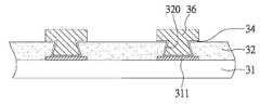
- the conductive layer 34has high conductivity, it is used as an electrical conduction path during an electroplating process to form a conductive element 36 on the electrically connecting pad 311 in the opening 350 of the resist layer 35 and the opening 320 of the insulating protective layer 32 .
- the opening 320which is tapered upward enables a relatively large contact area between the conductive element 36 and the electrically connecting pad 311 , thereby increasing shear stress.
- the conductive element 36can be perfectly fit in the insulating protective layer 32 through the tapered opening 320 ; as a result, the bonding strength is enhanced, and detachment of the conductive element 36 is prevented.
- the conductive element 36is, selectively, an alloy of any combinations of Pb, Sn, Ag, Au, Bi, Sb, Zn, Ni, Zr, Mg, In, Te and Ga.
- the resist layer 35 and the overlaying conductive layer 34are removed by mold release and etching. Since the process of removing the resist layer 35 and the conductive layer 34 are well known, the process is not described herein.
- a solder bump(not shown) is formed on the conductive element 36 by a reflow process for further electrical connection.
- the circuit board surface structure of the present inventioncomprises a circuit board 31 having at least one surface provided with a plurality of electrically connecting pads 311 , an insulating protective layer 32 formed on the surface of the circuit board 31 with upwardly-tapered openings 320 formed, by dry baking, exposure, and development, in the insulating protective layer 32 to expose the electrically connecting pads 311 .
- the insulating protective layer 32is made of a photosensitive dielectric material.
- the photosensitive dielectric materialis, selectively, a solder mask, a liquid photosensitive dielectric material, or a dry film photosensitive dielectric material.
- the liquid photosensitive dielectric materialis formed on the surface of the circuit board 31 by a non-printing means, such as roller coating, spray coating, dipping coating, and spin coating.
- the dry film photosensitive dielectric materialis laminated onto the surface of the circuit board 31 .
- the foregoing structurefurther comprises a conductive element 36 formed in the opening 320 of the insulating protective layer 32 and electrically connected to the electrically connecting pad 311 .
- the conductive element 36is a solder, which is made of a material selected from any of the following: Sn, Sn—Ag, Sn—Ag—Cu, Sn—Pb, and Sn—Cu.
- the foregoing structurefurther comprises a conductive layer 34 formed between the conductive element 36 and the electrically connecting pad 311 .
- the conductive layer 34is made of a material selected from the following: Cu, Sn, Ni, Cr, Ti, Cu—Cr, and Sn—Pb.
- the conductive layercan be made of a conductive polymer.
- the circuit board surface structure of the present inventionmainly involves forming a solder mask layer on the circuit board having electrically connecting pads, then through exposure and development processes with quantitative control of heat and light, upwardly-tapered openings are formed in the insulating protective layer, allowing the electrically connecting pads 31 to have a relatively large exposed contact area, so as to increase the contact area between the conductive elements and the electrically connecting pads, and reinforce bonding between the conductive elements in the openings of the insulating protective layer and the electrically connecting pads.
- the present inventionprovides sufficient bonding strength for the conductive elements formed on the fine pitch electrically connecting pads, thereby overcoming a drawback of the prior art, that is, difficulty in attaching a solder material to the surface of an electrically connecting pad.
Landscapes
- Engineering & Computer Science (AREA)
- Microelectronics & Electronic Packaging (AREA)
- Manufacturing & Machinery (AREA)
- Physics & Mathematics (AREA)
- Condensed Matter Physics & Semiconductors (AREA)
- General Physics & Mathematics (AREA)
- Computer Hardware Design (AREA)
- Power Engineering (AREA)
- Non-Metallic Protective Coatings For Printed Circuits (AREA)
- Electric Connection Of Electric Components To Printed Circuits (AREA)
Abstract
Description
- 1. Field of the Invention
- The present invention relates to circuit board surface structures, and more particularly, to a circuit board surface structure comprising a circuit board with electrically connecting pads having conductive elements formed thereon for external electrical connection.
- 2. Description of the Prior Art
- According to flip chip technology nowadays, a semiconductor chip is electrically connected to a circuit board, in which electrode pads are provided on the active surface of the integrated circuit-equipped (IC-equipped) semiconductor chip, and the circuit board is provided with electrically connecting pads corresponding to the electrode pads. A solder structure or other conductive adhesive material is formed between the electrode pad of the semiconductor chip and the electrically connecting pad of the circuit board for providing electrical connection and mechanical coupling between the semiconductor chip and the circuit board.
- As shown in
FIG. 1 , in the flip chip technology, a plurality ofmetallic bumps 11 are formed on theelectrode pads 12 of a semiconductor chip and a plurality ofpre-solder structures 14 made of solder materials are formed on the electrically connectingpads 15 of acircuit board 16, then after a reflow soldering process, thepre-solder structures 14 are reflow soldered to the correspondingmetallic bumps 11, so as to form a plurality ofsolder points 17. Subsequently, anunderfill material 18 is provided between thesemiconductor chip 13 andcircuit board 16, coupling thesemiconductor chip 13 with thecircuit board 16, so as to ensure a satisfactory electrical connection. - Referring to
FIGS. 2A-2D , cross-sectional views illustrating the steps of depositing a solder material on electrically connecting pads of a circuit board are shown. As shown inFIG. 2A , acircuit board 20 having electrically connectingpads 201 on a surface thereof is provided, whereon a solder resisting layer such assolder mask layer 21 is applied on the surface of thecircuit board 20. Aphotomask 22 is formed above the electrically connectingpads 201, and through a series of exposure and development processes, openings are formed to expose the electrically connectingpads 201. In the exposure process, light rays which might otherwise travel straight on bend beneath theopaque region 22aof thephotomask 22 due to diffraction, as indicated by the direction S, such that part of thesolder mask layer 21 under thephotomask 22 is illuminated. Next, as shown inFIG. 2B , after the development process, theopening 210 is tapered downward. Subsequently, as shown inFIG. 2C , astencil board 23 having a plurality ofgrids 23ais disposed on thecircuit board 20, in which eachgrid 23aof thestencil board 23 is corresponding to each electrically connecting pad. A solder material is applied on the surface of thestencil board 23, followed by using aroller 24 to roll back and forth on thestencil board 23, or spraying the solder material (not shown) in eachgrid 23aof thestencil board 23 on each electrically connectingpad 201 after removal of thestencil board 23. As shown inFIG. 2D , then a reflow soldering process is performed to reflow solder the solder material to formsolder bumps 25 on the electrically connectingpads 201 of thecircuit board 20, such that solder structures can be successfully formed on the circuit board using a stencil printing technology. - However, in the demand of miniaturization and increased functionality of electronic products, the circuit layout is designed to be higher in density and the distance between each circuit layer is also shortened. Thus, a circuit board with high density of circuit layout must have a reduced circuit width and smaller electrically connecting pads. As a gap between the circuits is reduced, the opening on the solder mask layer above the electrically connecting pads must be miniaturized further, and this may reduce the contact area between the solder structure and electrically connecting pad, such that it is more difficult to form a solder material on the electrically connecting pad, thereby failing to satisfy the requirement for fine pitch of the electrically connecting pads in advanced electronic products.
- Moreover, as the opening210 of the
solder mask layer 21 is have a tapered downward shape, the bottom portion of thesolder bump 25 is smaller than the top portion thereof, causing a decrease in the contact area between thesolder bump 25 and the electrically connectingpad 201, thereby reducing the bonding between thesolder bump 25 and the electrically connectingpad 201. In addition, thesolder bump 25 in the opening210 of thesolder mask layer 21 is also tapered downward, but is not provided with any other coupling means, and thus thesolder bump 25 is likely to detach from the electrically connectingpad 201. - Accordingly, there is an urgent need for developing an electrical connection structure for circuit boards with a view to overcoming drawbacks of the prior art, namely difficulty in forming a solder structure on surfaces of electrically connecting pads, difficulty in meeting the requirements for a fine pitch between electrically connecting pads of advanced electronic products, and detachment of conductive elements.
- In light of the foregoing drawbacks of the prior art, a primary objective of the present invention is to provide a circuit board surface structure with enhanced bonding strength between the conductive elements and the circuit board.
- Another objective of the invention is to provide a circuit board surface structure such that the electrically connecting pads have a larger contact area for increasing the contact area between the conductive elements and the electrically connecting pads.
- In order to achieve the foregoing and other objectives, the circuit board surface structure comprises: a circuit board having a plurality of electrically connecting pads on at least one surface thereof; an insulating protective layer characterized by photosensitivity and a solder resisting function and formed on the surface of the circuit board; and openings formed in the insulating protective layer for exposing the electrically connecting pads on the circuit surface and tapered upward.
- According to the foregoing structure, the present invention further comprises a conductive element electroplated to the opening of the insulating protective layer for electrically connecting with the electrically connecting pad. The conductive element is made of a solder, such as Sn, Sn—Ag, Sn—Ag—Cu, Sn—Pb, and Sn—Cu. A conductive layer is formed between the conductive element and the electrically connecting pad. The conductive layer is made of a material selected from the following: Cu, Sn, Ni, Cr, Ti, Cu—Cr, and Sn—Pb. The conductive layer can be made of a conductive polymer.
- The insulating protective material is made of a photosensitive dielectric material. The photosensitive dielectric material is, selectively, a solder mask, a liquid photosensitive dielectric material, or a dry film photosensitive dielectric material. The liquid photosensitive dielectric material is formed on the surface of the circuit board by a non-printing means, such as roller coating, spray coating, dipping coating, and spin coating. The dry film photosensitive dielectric material is laminated onto the surface of the circuit board.
- In summary, the circuit board surface structure of the present invention, mainly involves forming a solder mask layer on the circuit board having electrically connecting pads, then through exposure and development process with quantitative control of heat and light, openings tapered upward are formed in the insulating protective layer, allowing the electrically connecting
pads 31 to have a larger exposed contact area, so as to increase the contact area between the conductive elements and the electrically connecting pads, and reinforce bonding between the conductive elements in the openings of the insulating protective layer and the electrically connecting pads. Moreover, the present invention provides sufficient bonding strength for the conductive elements formed on the fine pitch electrically connecting pads, thereby eliminating a drawback of the prior art, that is, difficulty in attaching a solder material to the surface of electrically connecting pads. - The present invention can be more fully understood by reading the following detailed description of the preferred embodiment, with reference made to the accompanying drawings, wherein:
FIG. 1 (PRIOR ART) is a cross-sectional view of a conventional flip chip structure;FIGS. 2A-2D (PRIOR ART) are cross-sectional views showing how to fabricate a conventional circuit board with conductive elements formed thereon in advance; andFIGS. 3A-3I are cross-sectional views showing how to fabricate a circuit board surface structure of the present invention.- The present invention is described in the following with specific embodiments, so that one skilled in the pertinent art can easily understand other advantages and effects of the present invention from the disclosure of the present invention.
FIGS. 3A-3I are cross-sectional views showing how to fabricate a circuit board surface structure of the present invention.- Referring to
FIG. 3A , acircuit board 31 resulted from a front end patterning process is provided. A plurality of electrically connectingpads 311, and optionally a plurality of conductive circuits (not shown), are formed on at least one surface of thecircuit board 31. There are numerous complicated processes of forming conductive circuits and electrically connecting pads on a circuit board. The processes are widely known by those skilled in the art, but are irrelevant to essential technical features of the present invention. Therefore, the processes are not described herein. - Referring to
FIG. 3B , an insulatingprotective layer 32 is formed on the surface of thecircuit board 31 having the electrically connectingpads 311. The insulatingprotective layer 32 is cured by a heating process such as dry baking. The insulatingprotective layer 32 is made of a photosensitive dielectric material. The photosensitive dielectric material is, selectively, a solder mask, a liquid photosensitive dielectric material, or a dry film photosensitive dielectric material. The liquid photosensitive dielectric material is formed on the surface of thecircuit board 31 by a non-printing means, such as roller coating, spray coating, dipping coating, and spin coating. The dry film photosensitive dielectric material is formed on the surface of thecircuit board 31 by lamination. - Referring to
FIG. 3C , aphotomask 33 having anopaque region 33ais disposed on the surface of the insulatingprotective layer 32. Theopaque region 33aof thephotomask 33 corresponds in position to the electrically connectingpads 311 of thecircuit board 31. Afterward, an exposure process begins, wherein light rays which might otherwise travel straight on bend beneath theopaque region 33adue to diffraction, resulting in a diffraction effect line S, such that part of the insulatingprotective layer 32 beneath theopaque region 33ais illuminated. At the process when light penetrates the insulatingprotective layer 32, light energy is absorbed by the insulatingprotective layer 32, thereby resulting in a cross linking reaction. The cross linking reaction takes place more markedly at the surface of the insulatingprotective layer 32 than the bottom of the insulatingprotective layer 32; in other words, the effect of diffraction decreases with the distance traveled by the penetrating light rays in the insulatingprotective layer 32, as indicated by a distance effect line D. Monomers in a portion of the insulatingprotective layer 32 not covered by thephotomask 33 undergo a light energy-dependent reaction to form a complete cross-linked polymer, so as to form ahardened region 32aby curing. A portion of the insulatingprotective layer 32 covered by thephotomask 33 is referred to as anon-hardened region 32bfree of any light energy-dependent reaction. A portion of the insulatingprotective layer 32 between the diffraction effect line S and the distance effect line D is referred to as a half-hardenedregion 32ccharacterized by half cross linking in an incomplete light energy-dependent reaction. It should be noted that a process parameter can be modified, for example, properly reducing the energy level of light irradiation, to alter the curve of the diffraction effect line S, such that diffraction has a greater impact on the surface of the insulatingprotective layer 32 than the bottom of the insulatingprotective layer 32. - Referring to
FIG. 3D , thephotomask 33 is removed to expose the surface of the insulatingprotective layer 32, and then thenon-hardened region 32bis dissolvedly removed by a development process. - Referring to
FIG. 3E , the dissolving time is lengthened to further dissolvedly remove the half-hardenedregion 32c, so as to form an upwardly-taperedopening 320. Afterward, a portion of the half-hardenedregion 32cwhich has not been completely dissolvedly removed is completely cured by means of light energy and heat energy, so as to finalize the shaping of theopening 320. - Referring to
FIG. 3F , aconductive layer 34 is formed on the surface of the insulatingprotective layer 32 and in theopening 320. Theconductive layer 34 which functions as an electrical current conductive path required for a metal undergoing a subsequent electroplating process is implemented as a metal, an alloy, or a plurality of deposited metal layers, comprising Cu, Sn, Ni, Cr, Ti, Cu—Cr alloy, or Sn—Pb alloy. Alternatively, theconductive layer 34 can be made of a conductive polymer, such as polyacetylene, polyaniline, and organic sulfur polymer. - Referring to
FIG. 3G , a resistlayer 35 is formed on the surface of theconductive layer 34, andopenings 350 are formed in the resistlayer 35 to expose theconductive layer 34 on the surface of the electrically connectingpads 311. The resistlayer 35 can be a dry film or liquid photoresist layer formed on the surface of theconductive layer 34 by printing, spin coating, or adhesion; afterward, the resistlayer 35 is patterned by exposure and development to form theopenings 350. - Referring to
FIG. 3H , an electroplating process is performed on thecircuit board 31. Since theconductive layer 34 has high conductivity, it is used as an electrical conduction path during an electroplating process to form aconductive element 36 on the electrically connectingpad 311 in theopening 350 of the resistlayer 35 and theopening 320 of the insulatingprotective layer 32. Theopening 320 which is tapered upward enables a relatively large contact area between theconductive element 36 and the electrically connectingpad 311, thereby increasing shear stress. Moreover theconductive element 36 can be perfectly fit in the insulatingprotective layer 32 through thetapered opening 320; as a result, the bonding strength is enhanced, and detachment of theconductive element 36 is prevented. Theconductive element 36 is, selectively, an alloy of any combinations of Pb, Sn, Ag, Au, Bi, Sb, Zn, Ni, Zr, Mg, In, Te and Ga. - Referring to
FIG. 31 , lastly, the resistlayer 35 and the overlayingconductive layer 34 are removed by mold release and etching. Since the process of removing the resistlayer 35 and theconductive layer 34 are well known, the process is not described herein. - Where the
conductive element 36 is a solder, a solder bump (not shown) is formed on theconductive element 36 by a reflow process for further electrical connection. - The circuit board surface structure of the present invention comprises a
circuit board 31 having at least one surface provided with a plurality of electrically connectingpads 311, an insulatingprotective layer 32 formed on the surface of thecircuit board 31 with upwardly-taperedopenings 320 formed, by dry baking, exposure, and development, in the insulatingprotective layer 32 to expose the electrically connectingpads 311. - The insulating
protective layer 32 is made of a photosensitive dielectric material. The photosensitive dielectric material is, selectively, a solder mask, a liquid photosensitive dielectric material, or a dry film photosensitive dielectric material. The liquid photosensitive dielectric material is formed on the surface of thecircuit board 31 by a non-printing means, such as roller coating, spray coating, dipping coating, and spin coating. The dry film photosensitive dielectric material is laminated onto the surface of thecircuit board 31. - The foregoing structure further comprises a
conductive element 36 formed in theopening 320 of the insulatingprotective layer 32 and electrically connected to the electrically connectingpad 311. Theconductive element 36 is a solder, which is made of a material selected from any of the following: Sn, Sn—Ag, Sn—Ag—Cu, Sn—Pb, and Sn—Cu. - The foregoing structure further comprises a
conductive layer 34 formed between theconductive element 36 and the electrically connectingpad 311. Theconductive layer 34 is made of a material selected from the following: Cu, Sn, Ni, Cr, Ti, Cu—Cr, and Sn—Pb. The conductive layer can be made of a conductive polymer. - The circuit board surface structure of the present invention, mainly involves forming a solder mask layer on the circuit board having electrically connecting pads, then through exposure and development processes with quantitative control of heat and light, upwardly-tapered openings are formed in the insulating protective layer, allowing the electrically connecting
pads 31 to have a relatively large exposed contact area, so as to increase the contact area between the conductive elements and the electrically connecting pads, and reinforce bonding between the conductive elements in the openings of the insulating protective layer and the electrically connecting pads. The present invention provides sufficient bonding strength for the conductive elements formed on the fine pitch electrically connecting pads, thereby overcoming a drawback of the prior art, that is, difficulty in attaching a solder material to the surface of an electrically connecting pad. - The present invention has been described using exemplary preferred embodiments. However, it is to be understood that the scope of the present invention is not limited to the disclosed embodiments. On the contrary, it is intended to cover various modifications and similar arrangements. The scope of the claims, therefore, should be accorded the broadest interpretation so as to encompass all such modifications and similar arrangements.
Claims (12)
Applications Claiming Priority (3)
| Application Number | Priority Date | Filing Date | Title |
|---|---|---|---|
| TW096107788 | 2007-03-07 | ||
| TW096107788ATWI331494B (en) | 2007-03-07 | 2007-03-07 | Circuit board structure |
| TW96107788A | 2007-03-07 |
Publications (2)
| Publication Number | Publication Date |
|---|---|
| US20080217047A1true US20080217047A1 (en) | 2008-09-11 |
| US8058564B2 US8058564B2 (en) | 2011-11-15 |
Family
ID=39740495
Family Applications (1)
| Application Number | Title | Priority Date | Filing Date |
|---|---|---|---|
| US12/043,689Expired - Fee RelatedUS8058564B2 (en) | 2007-03-07 | 2008-03-06 | Circuit board surface structure |
Country Status (2)
| Country | Link |
|---|---|
| US (1) | US8058564B2 (en) |
| TW (1) | TWI331494B (en) |
Cited By (12)
| Publication number | Priority date | Publication date | Assignee | Title |
|---|---|---|---|---|
| US20080176035A1 (en)* | 2007-01-24 | 2008-07-24 | Phoenix Precision Technology Corporation | Circuit board structure and fabrication method of the same |
| US20100139963A1 (en)* | 2008-12-10 | 2010-06-10 | Nec Electronics Corporation | Interconnect substrate, method of manufacturing interconnect substrate and semiconductor device |
| US20120006591A1 (en)* | 2010-07-08 | 2012-01-12 | Kentaro Kaneko | Wiring Substrate and Method for Manufacturing Wiring Substrate |
| US20120222894A1 (en)* | 2011-03-04 | 2012-09-06 | Shinko Electric Industries Co., Ltd. | Wiring substrate and method for manufacturing wiring substrates |
| DE102011086546A1 (en)* | 2011-11-17 | 2013-05-23 | Osram Opto Semiconductors Gmbh | Optoelectronic component i.e. high power-LED, and printed circuit board i.e. metal printed circuit board, arrangement for use in e.g. monitor, has fastening devices for fastening component to board, where one of devices has polymer-layer |
| US20160013162A1 (en)* | 2010-05-20 | 2016-01-14 | Taiwan Semiconductor Manufacturing Company, Ltd. | Substrate Interconnections having Different Sizes |
| US20160113114A1 (en)* | 2013-05-07 | 2016-04-21 | Unimicron Technology Corp. | Carrier substrate |
| US9953939B2 (en) | 2012-09-18 | 2018-04-24 | Taiwan Semiconductor Manufacturing Company, Ltd. | Conductive contacts having varying widths and method of manufacturing same |
| US9991224B2 (en) | 2012-04-18 | 2018-06-05 | Taiwan Semiconductor Manufacturing Company, Ltd. | Bump-on-trace interconnect having varying widths and methods of forming same |
| US10056345B2 (en) | 2012-04-17 | 2018-08-21 | Taiwan Semiconductor Manufacturing Company, Ltd. | Conical-shaped or tier-shaped pillar connections |
| CN110493972A (en)* | 2019-08-23 | 2019-11-22 | 江苏上达电子有限公司 | A kind of reinforcement for COF |
| WO2023239172A1 (en)* | 2022-06-08 | 2023-12-14 | 엘지이노텍 주식회사 | Semiconductor package |
Families Citing this family (2)
| Publication number | Priority date | Publication date | Assignee | Title |
|---|---|---|---|---|
| JP2014049608A (en)* | 2012-08-31 | 2014-03-17 | Ibiden Co Ltd | Printed wiring board and method of manufacturing the same |
| TWI812977B (en)* | 2021-07-16 | 2023-08-21 | 欣興電子股份有限公司 | Circuit board enhancing structure and manufacture method thereof |
Citations (5)
| Publication number | Priority date | Publication date | Assignee | Title |
|---|---|---|---|---|
| US5858824A (en)* | 1996-06-14 | 1999-01-12 | Nec Corporation | Method of forming fine electrode on semiconductor substrate |
| US20060252248A1 (en)* | 2005-05-09 | 2006-11-09 | Wen-Hung Hu | Method for fabricating electrically connecting structure of circuit board |
| US20060278997A1 (en)* | 2004-12-01 | 2006-12-14 | Tessera, Inc. | Soldered assemblies and methods of making the same |
| US20060279881A1 (en)* | 2005-06-08 | 2006-12-14 | Kiyoshi Sato | Tunneling magnetic sensing element having two-layer insulating film and method for fabricating same |
| US20100085997A1 (en)* | 2008-10-07 | 2010-04-08 | Sanyo Electric Co., Ltd. | Nitride-based semiconductor laser device and method of manufacturing the same |
- 2007
- 2007-03-07TWTW096107788Apatent/TWI331494B/ennot_activeIP Right Cessation
- 2008
- 2008-03-06USUS12/043,689patent/US8058564B2/ennot_activeExpired - Fee Related
Patent Citations (5)
| Publication number | Priority date | Publication date | Assignee | Title |
|---|---|---|---|---|
| US5858824A (en)* | 1996-06-14 | 1999-01-12 | Nec Corporation | Method of forming fine electrode on semiconductor substrate |
| US20060278997A1 (en)* | 2004-12-01 | 2006-12-14 | Tessera, Inc. | Soldered assemblies and methods of making the same |
| US20060252248A1 (en)* | 2005-05-09 | 2006-11-09 | Wen-Hung Hu | Method for fabricating electrically connecting structure of circuit board |
| US20060279881A1 (en)* | 2005-06-08 | 2006-12-14 | Kiyoshi Sato | Tunneling magnetic sensing element having two-layer insulating film and method for fabricating same |
| US20100085997A1 (en)* | 2008-10-07 | 2010-04-08 | Sanyo Electric Co., Ltd. | Nitride-based semiconductor laser device and method of manufacturing the same |
Cited By (26)
| Publication number | Priority date | Publication date | Assignee | Title |
|---|---|---|---|---|
| US7948085B2 (en)* | 2007-01-24 | 2011-05-24 | Unimicron Technology Corp. | Circuit board structure |
| US20080176035A1 (en)* | 2007-01-24 | 2008-07-24 | Phoenix Precision Technology Corporation | Circuit board structure and fabrication method of the same |
| US8367939B2 (en)* | 2008-12-10 | 2013-02-05 | Renesas Electronics Corporation | Interconnect substrate, method of manufacturing interconnect substrate and semiconductor device |
| US20100139963A1 (en)* | 2008-12-10 | 2010-06-10 | Nec Electronics Corporation | Interconnect substrate, method of manufacturing interconnect substrate and semiconductor device |
| US20160013162A1 (en)* | 2010-05-20 | 2016-01-14 | Taiwan Semiconductor Manufacturing Company, Ltd. | Substrate Interconnections having Different Sizes |
| US9773755B2 (en)* | 2010-05-20 | 2017-09-26 | Taiwan Semiconductor Manufacturing Company, Ltd. | Substrate interconnections having different sizes |
| US20120006591A1 (en)* | 2010-07-08 | 2012-01-12 | Kentaro Kaneko | Wiring Substrate and Method for Manufacturing Wiring Substrate |
| US20120222894A1 (en)* | 2011-03-04 | 2012-09-06 | Shinko Electric Industries Co., Ltd. | Wiring substrate and method for manufacturing wiring substrates |
| US9236334B2 (en)* | 2011-03-04 | 2016-01-12 | Shinko Electric Industries Co., Ltd. | Wiring substrate and method for manufacturing wiring substrates |
| DE102011086546A1 (en)* | 2011-11-17 | 2013-05-23 | Osram Opto Semiconductors Gmbh | Optoelectronic component i.e. high power-LED, and printed circuit board i.e. metal printed circuit board, arrangement for use in e.g. monitor, has fastening devices for fastening component to board, where one of devices has polymer-layer |
| US10056345B2 (en) | 2012-04-17 | 2018-08-21 | Taiwan Semiconductor Manufacturing Company, Ltd. | Conical-shaped or tier-shaped pillar connections |
| US11315896B2 (en) | 2012-04-17 | 2022-04-26 | Taiwan Semiconductor Manufacturing Company, Ltd. | Conical-shaped or tier-shaped pillar connections |
| US11682651B2 (en) | 2012-04-18 | 2023-06-20 | Taiwan Semiconductor Manufacturing Company | Bump-on-trace interconnect |
| US10847493B2 (en) | 2012-04-18 | 2020-11-24 | Taiwan Semiconductor Manufacturing, Ltd. | Bump-on-trace interconnect |
| US9991224B2 (en) | 2012-04-18 | 2018-06-05 | Taiwan Semiconductor Manufacturing Company, Ltd. | Bump-on-trace interconnect having varying widths and methods of forming same |
| US10510710B2 (en) | 2012-04-18 | 2019-12-17 | Taiwan Semiconductor Manufacturing Company, Ltd. | Bump-on-trace interconnect |
| US9953939B2 (en) | 2012-09-18 | 2018-04-24 | Taiwan Semiconductor Manufacturing Company, Ltd. | Conductive contacts having varying widths and method of manufacturing same |
| US10319691B2 (en) | 2012-09-18 | 2019-06-11 | Taiwan Semiconductor Manufacturing Company | Solderless interconnection structure and method of forming same |
| US10008459B2 (en) | 2012-09-18 | 2018-06-26 | Taiwan Semiconductor Manufacturing Company | Structures having a tapering curved profile and methods of making same |
| US9966346B2 (en) | 2012-09-18 | 2018-05-08 | Taiwan Semiconductor Manufacturing Company | Bump structure and method of forming same |
| US11043462B2 (en) | 2012-09-18 | 2021-06-22 | Taiwan Semiconductor Manufacturing Company | Solderless interconnection structure and method of forming same |
| US11961810B2 (en) | 2012-09-18 | 2024-04-16 | Taiwan Semiconductor Manufacturing Company | Solderless interconnection structure and method of forming same |
| US9491871B2 (en)* | 2013-05-07 | 2016-11-08 | Unimicron Technology Corp. | Carrier substrate |
| US20160113114A1 (en)* | 2013-05-07 | 2016-04-21 | Unimicron Technology Corp. | Carrier substrate |
| CN110493972A (en)* | 2019-08-23 | 2019-11-22 | 江苏上达电子有限公司 | A kind of reinforcement for COF |
| WO2023239172A1 (en)* | 2022-06-08 | 2023-12-14 | 엘지이노텍 주식회사 | Semiconductor package |
Also Published As
| Publication number | Publication date |
|---|---|
| TWI331494B (en) | 2010-10-01 |
| TW200838373A (en) | 2008-09-16 |
| US8058564B2 (en) | 2011-11-15 |
Similar Documents
| Publication | Publication Date | Title |
|---|---|---|
| US8058564B2 (en) | Circuit board surface structure | |
| US8164003B2 (en) | Circuit board surface structure and fabrication method thereof | |
| TWI450336B (en) | Copper pillar tin bump on semiconductor chip and method of forming of the same | |
| US7705456B2 (en) | Semiconductor package substrate | |
| US8671564B2 (en) | Substrate for flip chip bonding and method of fabricating the same | |
| TWI284947B (en) | Method of wafer level package using elastomeric electroplating mask | |
| US8269354B2 (en) | Semiconductor package substrate structure and manufacturing method thereof | |
| US20080185711A1 (en) | Semiconductor package substrate | |
| US20100132998A1 (en) | Substrate having metal post and method of manufacturing the same | |
| JP2006086194A (en) | Wiring board, manufacturing method therefor, and semiconductor device | |
| US20060225917A1 (en) | Conductive bump structure of circuit board and fabrication method thereof | |
| US7216424B2 (en) | Method for fabricating electrical connections of circuit board | |
| JP6949091B2 (en) | Circuit board structure and its manufacturing method | |
| JP2018082130A (en) | Wiring board and manufacturing method | |
| JP4729963B2 (en) | PROJECT ELECTRODE FOR CONNECTING ELECTRONIC COMPONENT, ELECTRONIC COMPONENT MOUNTING BODY USING SAME, AND METHOD FOR PRODUCING THEM | |
| CN101567355B (en) | Semiconductor packaging substrate and its manufacturing method | |
| US7341934B2 (en) | Method for fabricating conductive bump of circuit board | |
| JP5585354B2 (en) | Manufacturing method of semiconductor package | |
| CN108811301B (en) | Circuit board structure and manufacturing method thereof | |
| JP3568869B2 (en) | Semiconductor integrated circuit device and method of manufacturing the same | |
| US20060223299A1 (en) | Fabricating process of an electrically conductive structure on a circuit board | |
| KR101163987B1 (en) | Method for fabricating solder on pad of fine bump using photoresist | |
| TW201316864A (en) | Printed circuit board and method of manufacturing the same | |
| JPS62290154A (en) | Formation of solder bump electrode | |
| TW200837848A (en) | Method for fabricating semiconductor packaging substrate |
Legal Events
| Date | Code | Title | Description |
|---|---|---|---|
| AS | Assignment | Owner name:PHOENIX PRECISION TECHNOLOGY CORPORATION, TAIWAN Free format text:ASSIGNMENT OF ASSIGNORS INTEREST;ASSIGNOR:HU, WEN-HUNG;REEL/FRAME:020612/0322 Effective date:20080227 | |
| AS | Assignment | Owner name:UNIMICRON TECHNOLOGY CORP., TAIWAN Free format text:MERGER;ASSIGNOR:PHOENIX PRECISION TECHNOLOGY CORPORATION;REEL/FRAME:027010/0832 Effective date:20100108 | |
| STCF | Information on status: patent grant | Free format text:PATENTED CASE | |
| FPAY | Fee payment | Year of fee payment:4 | |
| FEPP | Fee payment procedure | Free format text:MAINTENANCE FEE REMINDER MAILED (ORIGINAL EVENT CODE: REM.); ENTITY STATUS OF PATENT OWNER: LARGE ENTITY | |
| LAPS | Lapse for failure to pay maintenance fees | Free format text:PATENT EXPIRED FOR FAILURE TO PAY MAINTENANCE FEES (ORIGINAL EVENT CODE: EXP.); ENTITY STATUS OF PATENT OWNER: LARGE ENTITY | |
| STCH | Information on status: patent discontinuation | Free format text:PATENT EXPIRED DUE TO NONPAYMENT OF MAINTENANCE FEES UNDER 37 CFR 1.362 | |
| FP | Lapsed due to failure to pay maintenance fee | Effective date:20191115 |