US20080212369A1 - Method of managing a memory device employing three-level cells - Google Patents
Method of managing a memory device employing three-level cellsDownload PDFInfo
- Publication number
- US20080212369A1 US20080212369A1US12/039,268US3926808AUS2008212369A1US 20080212369 A1US20080212369 A1US 20080212369A1US 3926808 AUS3926808 AUS 3926808AUS 2008212369 A1US2008212369 A1US 2008212369A1
- Authority
- US
- United States
- Prior art keywords
- level
- pair
- strings
- cells
- state corresponding
- Prior art date
- Legal status (The legal status is an assumption and is not a legal conclusion. Google has not performed a legal analysis and makes no representation as to the accuracy of the status listed.)
- Granted
Links
- 238000000034methodMethods0.000titleclaimsabstractdescription19
- 238000009826distributionMethods0.000description6
- 230000007704transitionEffects0.000description5
- 230000014759maintenance of locationEffects0.000description2
- XUIMIQQOPSSXEZ-UHFFFAOYSA-NSiliconChemical compound[Si]XUIMIQQOPSSXEZ-UHFFFAOYSA-N0.000description1
- 230000000694effectsEffects0.000description1
- 238000004193electrokinetic chromatographyMethods0.000description1
- 230000006870functionEffects0.000description1
- 238000007726management methodMethods0.000description1
- 239000004065semiconductorSubstances0.000description1
- 229910052710siliconInorganic materials0.000description1
- 239000010703siliconSubstances0.000description1
Images


Classifications
- G—PHYSICS
- G11—INFORMATION STORAGE
- G11C—STATIC STORES
- G11C16/00—Erasable programmable read-only memories
- G11C16/02—Erasable programmable read-only memories electrically programmable
- G11C16/06—Auxiliary circuits, e.g. for writing into memory
- G11C16/34—Determination of programming status, e.g. threshold voltage, overprogramming or underprogramming, retention
- G11C16/3436—Arrangements for verifying correct programming or erasure
Definitions
- This inventionrelates to semiconductor memory devices and, in particular, to a method of managing a memory that employs three-level cells.
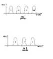
- cellsIn a multi-level memory device, cells generally assume more than two logic states and thus may store more than one bit of information. In a four-level memory cell, each cell is capable of storing two-bit of information by fixing its threshold voltage according to the distribution depicted in FIG. 1 .
- the state ‘ 11 ’is stored by an erasing operation, and the other three states (‘ 10 ’, ‘ 01 ’ and ‘ 00 ’) are stored by a programming operation.
- an error correction code (ECC) techniqueis used by reserving a number of memory cells, commonly called correction cells, the content of which is determined as a function of data stored in the cells of the array, in order to correct an eventual loss of information.
- ECCerror correction code
- NOR FLASH memory devicesin which a page of data at the time, typically having 4, 8 or 16 words, is read, for each page there is a certain number k of correction cells; the larger the value of k, the larger the number of bits that can be corrected on the page.
- a drawback of this approachis that the ECC limits the operations that may be executed by users.
- NOR FLASH memory deviceit is possible to carry out a program operation on a single cell, but an erase operation may be executed in parallel on all the cells of a sector.
- the presence of cells for storing the correction bit ECCmay not allow users to carry out a program operation on each page without erasing the whole memory sector. Indeed, a program operation (1 ⁇ 0) may imply erasing (0 ⁇ 1) in at least a correction cell. As stated before, this may not be done on a single cell of a NOR FLASH memory device, but on the whole addressed sector to which the cell belongs. As a consequence, the use of ECCs in NOR FLASH memory devices may strongly limit the so-called “bit manipulation,” i.e. the possibility of programming single bits of the memory.
- a three-level memory devicethat occupies a silicon area slightly larger than that of four-level memory devices of the same storage capacity, but that practically avoids the above remarked ECC limitations, is described in the Italian patent application VA2006A000065, in the name of the same applicant.
- the disclosed deviceemploys three-level cells in which each pair of cells is to store a string of three bits and comprises a coding circuit and a decoding circuit for converting, in a write operation, the strings of three bits to be stored in strings of two ternary values to be written in respective pairs of three-level cells and vice versa during a read operation.
- the possible states that may be assumed by the cellsare three, thus the relative distributions of the read thresholds, as depicted in FIG. 2 , may be relatively farther away from the voltage levels at which the “read disturb” and “retention” phenomena become more severe.
- the disclosed three-level memory deviceis burdened by problems that may be created by accidental supply voltage interruptions or significant voltage drops during programming operations.
- an accidental voltage drop or supply interruption sufficient to stop the program operationmay occur when the threshold voltage Vth is still within the distribution corresponding to the level 10 .
- a transition 11 ⁇ 10takes place and it may be no longer possible to further program the cell to the state 01 because the transition 10 ⁇ 01, even if physically possible, violates the “bit manipulation” rules and is impeded by the control circuits of the memory. Repeating the same program operation would not solve the problem, because the cell would go from state 10 to state 00 .
- An approachwould be that of carrying out an erase operation for bringing the cell from the state 10 back to the state 11 and then repeating the program operation. This may be inconvenient, particularly in NOR FLASH memory devices, wherein erase operations may be carried out on a whole memory sector and not on a single cell.
- a bit at logic level 1may be programmed to the logic level 0 but the opposite cannot be done through a program operation.
- a management method of a memory device including three-level cellsmay ensure that an eventual interruption of a program operation may not leave pairs of memory cells in an intermediate program state from which it would not be possible to reach the desired final state without violating the rules of “bit manipulation.”
- triplets of bitsare encoded in pairs of cells according to certain encoding schemes, it is possible to correctly program pairs of cells even if a power supply failure or other accidental event untimely stops the program operation.
- strings of three bitsare encoded in pairs of three-level cells according to the following code.
- FIG. 1depicts a distribution of threshold of memory cells that store two bits, according to the prior art
- FIG. 2depicts a sample distribution of the thresholds of a three-level cells of a memory device, according to the prior art
- FIG. 3illustrates schematically the effects of a supply voltage interruption during a program operation of a four-level cell, according to the prior art
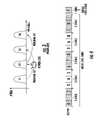
- FIG. 4depicts a sample coding of a word having 16 bits in eleven three-level-cells, in accordance with the present invention
- FIG. 5depicts possible transitions of a string of two ternary symbols according to a first coding scheme of the present invention.
- Encoding nine possible pairs of levels in eight possible combinations of triplets of bitsmay ensure the “bit manipulation” even in the case of NOR FLASH memory devices, that is it should be possible to program each of the three bits of each string stored in a pair of three-level cells. This is possible in a three-level memory device if a programming of 1, 2 or 3 bits of the triplets corresponds to programming three-level cells and not to erasing.
- the pair of three-level cellscan be programmed only in the state CC.
- the operation mentioned at point 1)may be completed correctly simply by repeating the interrupted program steps until the state CC is reached.
- the operation mentioned at point 2)may not be completed correctly if an interruption takes place while the pair of three-level cells is being programmed, if the three-level memory device is not properly managed.
- transition AA ⁇ CBis carried out through the following program operations:
Landscapes
- Read Only Memory (AREA)
- Control Of Amplification And Gain Control (AREA)
- Measurement Of Current Or Voltage (AREA)
Abstract
Description
- This invention relates to semiconductor memory devices and, in particular, to a method of managing a memory that employs three-level cells.
- In a multi-level memory device, cells generally assume more than two logic states and thus may store more than one bit of information. In a four-level memory cell, each cell is capable of storing two-bit of information by fixing its threshold voltage according to the distribution depicted in
FIG. 1 . The state ‘11’ is stored by an erasing operation, and the other three states (‘10’, ‘01’ and ‘00’) are stored by a programming operation. - In order to avoid the known problems of “read disturb” and “retention,” an error correction code (ECC) technique is used by reserving a number of memory cells, commonly called correction cells, the content of which is determined as a function of data stored in the cells of the array, in order to correct an eventual loss of information. For example, in NOR FLASH memory devices in which a page of data at the time, typically having 4, 8 or 16 words, is read, for each page there is a certain number k of correction cells; the larger the value of k, the larger the number of bits that can be corrected on the page.
- A drawback of this approach is that the ECC limits the operations that may be executed by users. In a NOR FLASH memory device, it is possible to carry out a program operation on a single cell, but an erase operation may be executed in parallel on all the cells of a sector.
- The presence of cells for storing the correction bit ECC may not allow users to carry out a program operation on each page without erasing the whole memory sector. Indeed, a program operation (1→0) may imply erasing (0→1) in at least a correction cell. As stated before, this may not be done on a single cell of a NOR FLASH memory device, but on the whole addressed sector to which the cell belongs. As a consequence, the use of ECCs in NOR FLASH memory devices may strongly limit the so-called “bit manipulation,” i.e. the possibility of programming single bits of the memory.
- A three-level memory device that occupies a silicon area slightly larger than that of four-level memory devices of the same storage capacity, but that practically avoids the above remarked ECC limitations, is described in the Italian patent application VA2006A000065, in the name of the same applicant.
- The disclosed device employs three-level cells in which each pair of cells is to store a string of three bits and comprises a coding circuit and a decoding circuit for converting, in a write operation, the strings of three bits to be stored in strings of two ternary values to be written in respective pairs of three-level cells and vice versa during a read operation.
- The possible states that may be assumed by the cells are three, thus the relative distributions of the read thresholds, as depicted in
FIG. 2 , may be relatively farther away from the voltage levels at which the “read disturb” and “retention” phenomena become more severe. - As may be common to all multi-level memory devices, the disclosed three-level memory device is burdened by problems that may be created by accidental supply voltage interruptions or significant voltage drops during programming operations.
- In order to better understand this peculiar challenge faced by multi-level memory devices, let us refer to the scheme of
FIG. 3 for a four-level cell capable of storing two bits. - Supposing that an initially erased cell (11) is to be programmed in the
state 01, this operation is compliant with “bit manipulation” rules because only one bit may be programmed. The threshold voltage Vth of the cell may be incremented by applying program pulses to the cell, until its threshold is incremented to a value comprised in the distribution curve relative to thelevel 01. - As schematically illustrated in
FIG. 3 , an accidental voltage drop or supply interruption sufficient to stop the program operation may occur when the threshold voltage Vth is still within the distribution corresponding to thelevel 10. In this case, atransition 11→10 takes place and it may be no longer possible to further program the cell to thestate 01 because thetransition 10→01, even if physically possible, violates the “bit manipulation” rules and is impeded by the control circuits of the memory. Repeating the same program operation would not solve the problem, because the cell would go fromstate 10 tostate 00. - An approach would be that of carrying out an erase operation for bringing the cell from the
state 10 back to thestate 11 and then repeating the program operation. This may be inconvenient, particularly in NOR FLASH memory devices, wherein erase operations may be carried out on a whole memory sector and not on a single cell. In practice, in order to comply with the “bit manipulation” requisites, a bit atlogic level 1 may be programmed to thelogic level 0 but the opposite cannot be done through a program operation. - For this reason, when it is of paramount importance that data be correctly stored even in the event of a power failure during program operations, adjacent pairs of bits may be programmed, that is equivalent to programming a four-level cell to the
state 00. This is possible without violating the rules of “bit manipulation” because a four-level cell may be programmed in thestate 00 whether it is in thestate 10 or in thestate 01. - In the case of a three-level cell, it may be easily recognized that an accidental power failure may be dangerous if it took place during a program operation from A to C and if the threshold voltage of the cell at the moment of the failure corresponds to the level B.
- Therefore, a management method of a memory device including three-level cells may ensure that an eventual interruption of a program operation may not leave pairs of memory cells in an intermediate program state from which it would not be possible to reach the desired final state without violating the rules of “bit manipulation.”
- If triplets of bits are encoded in pairs of cells according to certain encoding schemes, it is possible to correctly program pairs of cells even if a power supply failure or other accidental event untimely stops the program operation.
- According to an embodiment, strings of three bits are encoded in pairs of three-level cells according to the following code.
111 AA 110 AB 101 BB 011 BA 010 AC o CA 100 BC 001 CB 000 CC
Pairs of cells are programmed according to the following sequence:- a) programming in the state C the least significant cells that are to reach this state,
- b) programming in the state B the most significant cells that are to reach this state or that pass through this state,
- c) programming in the state B the least significant cells that are to reach this state,
- d) programming in the state C the most significant cells that are to reach this state.
- According to an alternative embodiment, the following code is adopted:
111 AA 110 AB 101 BB 011 BA 010 AC o CA 100 CB 001 BC 000 CC
and the above specified operations from a) to d) are carried out by exchanging the roles of the most significant cells with the least significant cells.- It has been found that, with the above illustrated methods, a program operation can be completed correctly even in case of an accidental untimely interruption of the programming process by repeating the interrupted program operation.
- The invention is defined in the annexed claims.
- The invention will be described referring to the attached drawings, wherein:
FIG. 1 depicts a distribution of threshold of memory cells that store two bits, according to the prior art;FIG. 2 depicts a sample distribution of the thresholds of a three-level cells of a memory device, according to the prior art;FIG. 3 illustrates schematically the effects of a supply voltage interruption during a program operation of a four-level cell, according to the prior art;FIG. 4 depicts a sample coding of a word having 16 bits in eleven three-level-cells, in accordance with the present invention;FIG. 5 depicts possible transitions of a string of two ternary symbols according to a first coding scheme of the present invention.- In order to efficiently store bit strings in a three-level memory cell array, it is helpful to define a coding operation of binary strings in ternary strings that may be stored in three-level memory cells, and vice versa.
- ‘A, ‘B’, and ‘C’ being the three levels, depicted in
FIG. 4 , that each cell may assume (‘A’ is the erased level, ‘B’ and ‘C’ the two programmed levels), to each pair of cells (3×3=9 possible states) the information of 3 bits (23=8 possible combinations) is associated. - Encoding nine possible pairs of levels in eight possible combinations of triplets of bits may ensure the “bit manipulation” even in the case of NOR FLASH memory devices, that is it should be possible to program each of the three bits of each string stored in a pair of three-level cells. This is possible in a three-level memory device if a programming of 1, 2 or 3 bits of the triplets corresponds to programming three-level cells and not to erasing.
- For sake of clarity, reference will be made to the preferred coding scheme depicted in
FIG. 5 , though the same observations also hold for the following alternative coding scheme: 111 AA 110 AB 101 BB 011 BA 010 AC o CA 100 CB 001 BC 000 CC - Using the grouping scheme of
FIG. 4 of the three-level memory device, it is noticed that if two adjacent bits of a bit string are to be programmed (00) as in two-bit-per-cell memory devices, no pair of three-level cells may be programmed in the state BB, AC and CA, while all other states should be possible. Therefore, starting from a pair of erased three-level cells, that is in the state AA (111), the following cases are possible: - if two adjacent bits to be programmed (00) belong to the same triplet of bits, then the pair of three-level cells should be programmed to one of the states BC (100) and CB (001);
- if two adjacent bits to be programmed (00) belong one to a triplet of bits and the other to another triplet of bits adjacent to the first one, then the pair of three-level cells should be programmed to one of the states AB (110) and BA (011).
- Starting from a pair of three-level cells in the state AB (110) or BA (011), if the two adjacent bits to be programmed (00) belong to the same triplet of bits, then the pair of three-level cells should be programmed in the state CC (000). Evidently, starting from the states BC or CB, the pair of three-level cells can be programmed only in the state CC.
- Problems due to accidentally untimely interruption of a program operation arise if between the initial and final states of the pairs to be programmed, there is at least an intermediate state, in which the program operation can unduly stop. Recalling that a program operation of two adjacent bits (00) does reach the states BB, AC and CA for the above explained reasons, the program operations that contemplate transitions through an intermediate state are:
- 1) the program operations from a state AA, AB, or BA, in the state CC;
- 2) the program operations from the state AA either in the states CB or BC.
- Even if an accidental interruption takes place, the operation mentioned at point 1) may be completed correctly simply by repeating the interrupted program steps until the state CC is reached. By contrast, the operation mentioned at point 2) may not be completed correctly if an interruption takes place while the pair of three-level cells is being programmed, if the three-level memory device is not properly managed.
- Consider for example the program operation AA→CB. Both cells receive in parallel program pulses for reaching the state BB. Once the state BB has been reached, the less significant cell is deselected and program pulses are supplied to the most significant cell until it reaches the state BC. It may happen, though, that the most significant cell goes to the state B before the least significant cell and, if in such a situation an accidental interruption (e.g. a supply voltage interruption or severe drop) occurs, the program operation would be stopped with the pair of three-level cells in the state BA. From this state it may not be possible to go to the state BC without violating the rules of “bit manipulation”. The above exposed difficulty is also encountered, when programming from the state AA to the state CB.
- According to the method, to obviate to these drawbacks, the program operations mentioned at point 2) are executed by:
- a) programming to the state C the least significant cells that are to reach this state,
- b) programming to the state B the most significant cells that are to reach this state or that must pass through this state,
- c) programming to the state B the least significant cells that are to reach this state,
- d) programming to the state C the most significant cells that are to reach this state.
- In practice, the transition AA→CB is carried out through the following program operations:
- a) AA→AA;
- b) AA→BA;
- c) BA→BB;
- d) BB→CB.
- Another alternative valid coding scheme that can be adopted for solving the above described drawbacks is the following:
111 AA 110 AB 101 BB 011 BA 010 AC o CA 100 CB 001 BC 000 CC
and the sequence of operations to be carried out for programming a pair of cells may be:- a) programming to the state C the most significant cells that are to reach this state,
- b) programming to the state B the least significant cells that are to reach this state or that must pass through this state,
- c) programming to the state B the most significant cells that are to reach this state B,
- d) programming to the state C the least significant cells that are to reach this state.
- With the methods of this approach, difficulties due to eventual voltage interruptions (or due to any cause) of programming operation are overcome because the programming operations take place by changing a single level of the state of a single cell and the programming step d) may be correctly completed even if the arresting event takes place when the pairs of cells is in the intermediate state BB. Indeed, starting from the state BB it is possible to reach the state CB (BC) by changing of a single level the state of a single cell.
- According to the managing method of the memory device employing three-level cells, it is no longer helpful to implement an ECC technique for completing any program operation in case of an accidental untimely interruption of the process without violating the “bit manipulation” rules.
Claims (13)
Applications Claiming Priority (3)
| Application Number | Priority Date | Filing Date | Title |
|---|---|---|---|
| IT000026AITVA20070026A1 (en) | 2007-03-02 | 2007-03-02 | METHOD OF MANAGEMENT OF A TRI-LEVEL MEMORY |
| ITVA2007A0026 | 2007-03-02 | ||
| ITVA2007A000026 | 2007-03-02 |
Publications (2)
| Publication Number | Publication Date |
|---|---|
| US20080212369A1true US20080212369A1 (en) | 2008-09-04 |
| US7782665B2 US7782665B2 (en) | 2010-08-24 |
Family
ID=39732939
Family Applications (1)
| Application Number | Title | Priority Date | Filing Date |
|---|---|---|---|
| US12/039,268Expired - Fee RelatedUS7782665B2 (en) | 2007-03-02 | 2008-02-28 | Method of managing a memory device employing three-level cells |
Country Status (2)
| Country | Link |
|---|---|
| US (1) | US7782665B2 (en) |
| IT (1) | ITVA20070026A1 (en) |
Cited By (1)
| Publication number | Priority date | Publication date | Assignee | Title |
|---|---|---|---|---|
| US20100153820A1 (en)* | 2008-12-16 | 2010-06-17 | Emanuele Confalonieri | Memory with guard value dependent error correction |
Families Citing this family (2)
| Publication number | Priority date | Publication date | Assignee | Title |
|---|---|---|---|---|
| KR102305095B1 (en) | 2015-04-13 | 2021-09-24 | 삼성전자주식회사 | Method for operating non-volatile memory controller |
| JP2019040655A (en)* | 2017-08-28 | 2019-03-14 | 東芝メモリ株式会社 | Memory system |
Citations (6)
| Publication number | Priority date | Publication date | Assignee | Title |
|---|---|---|---|---|
| US5838610A (en)* | 1996-02-07 | 1998-11-17 | Nec Corporation | Semiconductor memory device having multilevel memory cell array |
| US5973958A (en)* | 1998-06-23 | 1999-10-26 | Advanced Micro Devices, Inc. | Interlaced storage and sense technique for flash multi-level devices |
| US6208542B1 (en)* | 1998-06-30 | 2001-03-27 | Sandisk Corporation | Techniques for storing digital data in an analog or multilevel memory |
| US7366001B2 (en)* | 2003-12-25 | 2008-04-29 | Hitachi, Ltd. | Content addressable memory including main-match lines and sub-match lines |
| US20080106937A1 (en)* | 2006-11-03 | 2008-05-08 | Stmicroelectronics S.R.I. | Memory device employing three-level cells and related methods of managing |
| US20080266946A1 (en)* | 2007-04-27 | 2008-10-30 | Stmicroelectronics S.R.I. | Method of managing a multilevel memory device and related device |
- 2007
- 2007-03-02ITIT000026Apatent/ITVA20070026A1/enunknown
- 2008
- 2008-02-28USUS12/039,268patent/US7782665B2/ennot_activeExpired - Fee Related
Patent Citations (6)
| Publication number | Priority date | Publication date | Assignee | Title |
|---|---|---|---|---|
| US5838610A (en)* | 1996-02-07 | 1998-11-17 | Nec Corporation | Semiconductor memory device having multilevel memory cell array |
| US5973958A (en)* | 1998-06-23 | 1999-10-26 | Advanced Micro Devices, Inc. | Interlaced storage and sense technique for flash multi-level devices |
| US6208542B1 (en)* | 1998-06-30 | 2001-03-27 | Sandisk Corporation | Techniques for storing digital data in an analog or multilevel memory |
| US7366001B2 (en)* | 2003-12-25 | 2008-04-29 | Hitachi, Ltd. | Content addressable memory including main-match lines and sub-match lines |
| US20080106937A1 (en)* | 2006-11-03 | 2008-05-08 | Stmicroelectronics S.R.I. | Memory device employing three-level cells and related methods of managing |
| US20080266946A1 (en)* | 2007-04-27 | 2008-10-30 | Stmicroelectronics S.R.I. | Method of managing a multilevel memory device and related device |
Cited By (4)
| Publication number | Priority date | Publication date | Assignee | Title |
|---|---|---|---|---|
| US20100153820A1 (en)* | 2008-12-16 | 2010-06-17 | Emanuele Confalonieri | Memory with guard value dependent error correction |
| US8645792B2 (en) | 2008-12-16 | 2014-02-04 | Micron Technology, Inc. | Memory with guard value dependent error correction |
| US20140149823A1 (en)* | 2008-12-16 | 2014-05-29 | Micron Technology, Inc. | Memory with guard value dependent error correction |
| US9026890B2 (en)* | 2008-12-16 | 2015-05-05 | Micron Technology, Inc. | Memory with guard value dependent error correction |
Also Published As
| Publication number | Publication date |
|---|---|
| ITVA20070026A1 (en) | 2008-09-03 |
| US7782665B2 (en) | 2010-08-24 |
Similar Documents
| Publication | Publication Date | Title |
|---|---|---|
| US8014207B2 (en) | Nonvolatile memory device and method of operating the same | |
| US8136014B2 (en) | Non-volatile semiconductor memory device | |
| US7995388B1 (en) | Data storage using modified voltages | |
| US8484519B2 (en) | Optimal programming levels for LDPC | |
| CN102667944B (en) | Non-volatile memory and method for managing errors through read-after-write and adaptive rewrite | |
| US7826277B2 (en) | Non-volatile memory device and method of operating the same | |
| US7355892B2 (en) | Partial page fail bit detection in flash memory devices | |
| US20200293398A1 (en) | Non volatile memory controller device and method for adjustment | |
| US20100199150A1 (en) | Data Storage In Analog Memory Cell Arrays Having Erase Failures | |
| US7782667B2 (en) | Method of operating a flash memory device | |
| US20140347924A1 (en) | Data storage in analog memory cells across word lines using a non-integer number of bits per cell | |
| US20150131380A1 (en) | Adaptive initial program voltage for non-volatile memory | |
| KR20070087556A (en) | Flash memory management method, memory device, system, computer-readable recording medium, non-volatile storage element array management method | |
| JP2011197957A (en) | Apparatus and method for decoding error correction code | |
| US8050103B2 (en) | Method of programming nonvolatile memory device | |
| US7596023B2 (en) | Memory device employing three-level cells and related methods of managing | |
| US7782665B2 (en) | Method of managing a memory device employing three-level cells | |
| CN113051100B (en) | A flash memory and its error bit counting detection system | |
| US8539141B2 (en) | Optimized flash memory access method and device | |
| KR102808555B1 (en) | A method for mapping bits to memory cells using sector spreading and device for performing the method | |
| US7710772B2 (en) | Method of managing a multilevel memory device and related device | |
| KR100898689B1 (en) | How to Program Nand Flash Memory Devices | |
| Qin | Fractional bits-per-cell for nand flash with low read latency | |
| US12437822B2 (en) | Memory device and reading method thereof | |
| CN113342570B (en) | Dual-target state elimination coding and decoding method adaptive to 3D TLC type NAND flash memory data storage |
Legal Events
| Date | Code | Title | Description |
|---|---|---|---|
| AS | Assignment | Owner name:STMICROELECTRONICS S.R.L., ITALY Free format text:ASSIGNMENT OF ASSIGNORS INTEREST;ASSIGNORS:TURBANTI, PAOLO;POIDOMANI, CARLA GIUSEPPINA;CONFALONIERI, EMANUELE;AND OTHERS;REEL/FRAME:022438/0719 Effective date:20080221 | |
| AS | Assignment | Owner name:NUMONYX B.V.,SWITZERLAND Free format text:ASSIGNMENT OF ASSIGNORS INTEREST;ASSIGNOR:STMICROELECTRONICS NV;REEL/FRAME:024053/0222 Effective date:20080330 Owner name:NUMONYX B.V., SWITZERLAND Free format text:ASSIGNMENT OF ASSIGNORS INTEREST;ASSIGNOR:STMICROELECTRONICS NV;REEL/FRAME:024053/0222 Effective date:20080330 | |
| AS | Assignment | Owner name:STMICROELECTRONICS NV,SWITZERLAND Free format text:ASSIGNMENT OF ASSIGNORS INTEREST;ASSIGNOR:STMICROELECTRONICS S.R.L.;REEL/FRAME:024201/0742 Effective date:20080206 Owner name:STMICROELECTRONICS NV, SWITZERLAND Free format text:ASSIGNMENT OF ASSIGNORS INTEREST;ASSIGNOR:STMICROELECTRONICS S.R.L.;REEL/FRAME:024201/0742 Effective date:20080206 | |
| AS | Assignment | Owner name:MICRON TECHNOLOGY, INC., IDAHO Free format text:ASSIGNMENT OF ASSIGNORS INTEREST;ASSIGNOR:NUMONYX B.V.;REEL/FRAME:029184/0540 Effective date:20120523 | |
| FPAY | Fee payment | Year of fee payment:4 | |
| AS | Assignment | Owner name:U.S. BANK NATIONAL ASSOCIATION, AS COLLATERAL AGENT, CALIFORNIA Free format text:SECURITY INTEREST;ASSIGNOR:MICRON TECHNOLOGY, INC.;REEL/FRAME:038669/0001 Effective date:20160426 Owner name:U.S. BANK NATIONAL ASSOCIATION, AS COLLATERAL AGEN Free format text:SECURITY INTEREST;ASSIGNOR:MICRON TECHNOLOGY, INC.;REEL/FRAME:038669/0001 Effective date:20160426 | |
| AS | Assignment | Owner name:MORGAN STANLEY SENIOR FUNDING, INC., AS COLLATERAL AGENT, MARYLAND Free format text:PATENT SECURITY AGREEMENT;ASSIGNOR:MICRON TECHNOLOGY, INC.;REEL/FRAME:038954/0001 Effective date:20160426 Owner name:MORGAN STANLEY SENIOR FUNDING, INC., AS COLLATERAL Free format text:PATENT SECURITY AGREEMENT;ASSIGNOR:MICRON TECHNOLOGY, INC.;REEL/FRAME:038954/0001 Effective date:20160426 | |
| AS | Assignment | Owner name:U.S. BANK NATIONAL ASSOCIATION, AS COLLATERAL AGENT, CALIFORNIA Free format text:CORRECTIVE ASSIGNMENT TO CORRECT THE REPLACE ERRONEOUSLY FILED PATENT #7358718 WITH THE CORRECT PATENT #7358178 PREVIOUSLY RECORDED ON REEL 038669 FRAME 0001. ASSIGNOR(S) HEREBY CONFIRMS THE SECURITY INTEREST;ASSIGNOR:MICRON TECHNOLOGY, INC.;REEL/FRAME:043079/0001 Effective date:20160426 Owner name:U.S. BANK NATIONAL ASSOCIATION, AS COLLATERAL AGEN Free format text:CORRECTIVE ASSIGNMENT TO CORRECT THE REPLACE ERRONEOUSLY FILED PATENT #7358718 WITH THE CORRECT PATENT #7358178 PREVIOUSLY RECORDED ON REEL 038669 FRAME 0001. ASSIGNOR(S) HEREBY CONFIRMS THE SECURITY INTEREST;ASSIGNOR:MICRON TECHNOLOGY, INC.;REEL/FRAME:043079/0001 Effective date:20160426 | |
| FEPP | Fee payment procedure | Free format text:MAINTENANCE FEE REMINDER MAILED (ORIGINAL EVENT CODE: REM.) | |
| AS | Assignment | Owner name:MICRON TECHNOLOGY, INC., IDAHO Free format text:RELEASE BY SECURED PARTY;ASSIGNOR:U.S. BANK NATIONAL ASSOCIATION, AS COLLATERAL AGENT;REEL/FRAME:047243/0001 Effective date:20180629 | |
| LAPS | Lapse for failure to pay maintenance fees | Free format text:PATENT EXPIRED FOR FAILURE TO PAY MAINTENANCE FEES (ORIGINAL EVENT CODE: EXP.); ENTITY STATUS OF PATENT OWNER: LARGE ENTITY | |
| STCH | Information on status: patent discontinuation | Free format text:PATENT EXPIRED DUE TO NONPAYMENT OF MAINTENANCE FEES UNDER 37 CFR 1.362 | |
| FP | Lapsed due to failure to pay maintenance fee | Effective date:20180824 | |
| AS | Assignment | Owner name:MICRON TECHNOLOGY, INC., IDAHO Free format text:RELEASE BY SECURED PARTY;ASSIGNOR:MORGAN STANLEY SENIOR FUNDING, INC., AS COLLATERAL AGENT;REEL/FRAME:050937/0001 Effective date:20190731 |