US20080211028A1 - Electro-static discharge protection device, semiconductor device, and method for manufacturing electro-static discharge protection device - Google Patents
Electro-static discharge protection device, semiconductor device, and method for manufacturing electro-static discharge protection deviceDownload PDFInfo
- Publication number
- US20080211028A1 US20080211028A1US12/034,173US3417308AUS2008211028A1US 20080211028 A1US20080211028 A1US 20080211028A1US 3417308 AUS3417308 AUS 3417308AUS 2008211028 A1US2008211028 A1US 2008211028A1
- Authority
- US
- United States
- Prior art keywords
- diffusion region
- gate electrode
- region
- electro
- substrate
- Prior art date
- Legal status (The legal status is an assumption and is not a legal conclusion. Google has not performed a legal analysis and makes no representation as to the accuracy of the status listed.)
- Granted
Links
Images


Classifications
- H—ELECTRICITY
- H01—ELECTRIC ELEMENTS
- H01L—SEMICONDUCTOR DEVICES NOT COVERED BY CLASS H10
- H01L21/00—Processes or apparatus adapted for the manufacture or treatment of semiconductor or solid state devices or of parts thereof
- H01L21/02—Manufacture or treatment of semiconductor devices or of parts thereof
- H01L21/04—Manufacture or treatment of semiconductor devices or of parts thereof the devices having potential barriers, e.g. a PN junction, depletion layer or carrier concentration layer
- H—ELECTRICITY
- H10—SEMICONDUCTOR DEVICES; ELECTRIC SOLID-STATE DEVICES NOT OTHERWISE PROVIDED FOR
- H10D—INORGANIC ELECTRIC SEMICONDUCTOR DEVICES
- H10D84/00—Integrated devices formed in or on semiconductor substrates that comprise only semiconducting layers, e.g. on Si wafers or on GaAs-on-Si wafers
- H—ELECTRICITY
- H01—ELECTRIC ELEMENTS
- H01L—SEMICONDUCTOR DEVICES NOT COVERED BY CLASS H10
- H01L23/00—Details of semiconductor or other solid state devices
- H01L23/58—Structural electrical arrangements for semiconductor devices not otherwise provided for, e.g. in combination with batteries
- H01L23/60—Protection against electrostatic charges or discharges, e.g. Faraday shields
- H—ELECTRICITY
- H10—SEMICONDUCTOR DEVICES; ELECTRIC SOLID-STATE DEVICES NOT OTHERWISE PROVIDED FOR
- H10D—INORGANIC ELECTRIC SEMICONDUCTOR DEVICES
- H10D62/00—Semiconductor bodies, or regions thereof, of devices having potential barriers
- H10D62/10—Shapes, relative sizes or dispositions of the regions of the semiconductor bodies; Shapes of the semiconductor bodies
- H10D62/17—Semiconductor regions connected to electrodes not carrying current to be rectified, amplified or switched, e.g. channel regions
- H10D62/351—Substrate regions of field-effect devices
- H10D62/357—Substrate regions of field-effect devices of FETs
- H10D62/364—Substrate regions of field-effect devices of FETs of IGFETs
- H10D62/378—Contact regions to the substrate regions
- H—ELECTRICITY
- H10—SEMICONDUCTOR DEVICES; ELECTRIC SOLID-STATE DEVICES NOT OTHERWISE PROVIDED FOR
- H10D—INORGANIC ELECTRIC SEMICONDUCTOR DEVICES
- H10D84/00—Integrated devices formed in or on semiconductor substrates that comprise only semiconducting layers, e.g. on Si wafers or on GaAs-on-Si wafers
- H10D84/01—Manufacture or treatment
- H10D84/0123—Integrating together multiple components covered by H10D12/00 or H10D30/00, e.g. integrating multiple IGBTs
- H10D84/0126—Integrating together multiple components covered by H10D12/00 or H10D30/00, e.g. integrating multiple IGBTs the components including insulated gates, e.g. IGFETs
- H10D84/013—Manufacturing their source or drain regions, e.g. silicided source or drain regions
- H10D84/0133—Manufacturing common source or drain regions between multiple IGFETs
- H—ELECTRICITY
- H10—SEMICONDUCTOR DEVICES; ELECTRIC SOLID-STATE DEVICES NOT OTHERWISE PROVIDED FOR
- H10D—INORGANIC ELECTRIC SEMICONDUCTOR DEVICES
- H10D84/00—Integrated devices formed in or on semiconductor substrates that comprise only semiconducting layers, e.g. on Si wafers or on GaAs-on-Si wafers
- H10D84/01—Manufacture or treatment
- H10D84/02—Manufacture or treatment characterised by using material-based technologies
- H10D84/03—Manufacture or treatment characterised by using material-based technologies using Group IV technology, e.g. silicon technology or silicon-carbide [SiC] technology
- H10D84/038—Manufacture or treatment characterised by using material-based technologies using Group IV technology, e.g. silicon technology or silicon-carbide [SiC] technology using silicon technology, e.g. SiGe
- H—ELECTRICITY
- H10—SEMICONDUCTOR DEVICES; ELECTRIC SOLID-STATE DEVICES NOT OTHERWISE PROVIDED FOR
- H10D—INORGANIC ELECTRIC SEMICONDUCTOR DEVICES
- H10D89/00—Aspects of integrated devices not covered by groups H10D84/00 - H10D88/00
- H10D89/60—Integrated devices comprising arrangements for electrical or thermal protection, e.g. protection circuits against electrostatic discharge [ESD]
- H10D89/601—Integrated devices comprising arrangements for electrical or thermal protection, e.g. protection circuits against electrostatic discharge [ESD] for devices having insulated gate electrodes, e.g. for IGFETs or IGBTs
- H10D89/811—Integrated devices comprising arrangements for electrical or thermal protection, e.g. protection circuits against electrostatic discharge [ESD] for devices having insulated gate electrodes, e.g. for IGFETs or IGBTs using FETs as protective elements
- H—ELECTRICITY
- H10—SEMICONDUCTOR DEVICES; ELECTRIC SOLID-STATE DEVICES NOT OTHERWISE PROVIDED FOR
- H10D—INORGANIC ELECTRIC SEMICONDUCTOR DEVICES
- H10D30/00—Field-effect transistors [FET]
- H10D30/60—Insulated-gate field-effect transistors [IGFET]
- H10D30/601—Insulated-gate field-effect transistors [IGFET] having lightly-doped drain or source extensions, e.g. LDD IGFETs or DDD IGFETs
Definitions
- the present disclosurerelates to a semiconductor device, and more specifically, to a semiconductor device including an electro-static discharge protection device.
- a typical semiconductor deviceincludes an electro-static discharge (ESD) protection circuit to protect semiconductor elements from an external ESD surge.
- ESDelectro-static discharge
- the formation of a p + diffusion region in a drain region at a deep portion of a substrateis known as a method for enhancing ESD robustness of an electro-static discharge element in an ESD protection circuit.
- the AC characteristicsvary during normal operation of an IO cell depending on the accuracy of the p + diffusion region formation process. Accordingly, there is a demand for an ESD protection circuit having fixed AC characteristics and increased ESD.
- FIGS. 1 to 3show a semiconductor device including an ESD-protection-driver circuit employing the single gate electro-static discharge element of the prior art.
- a semiconductor device 100includes an input/output pad 110 coupled to an internal circuit 120 by wiring W 10 .
- the input/output pad 110is also coupled to an ESD-protection-driver circuit 130 by the wiring W 10 .
- the ESD protection circuit/drive circuit 130includes a plurality of single gate electro-static discharge elements M 10 that are coupled in parallel to one another.
- Each electro-static discharge element M 10includes a ballast resistor R and an N-channel MOS transistor T 10 , which is coupled in series with the ballast resistor R.
- the single gate electro-static discharge element M 10includes a gate electrode 142 arranged on a substrate 140 of p ⁇ silicon or the like by way of a gate oxidation film.
- a source region 145 S and a drain region 145 D including n + diffusion regionsare formed in the substrate 140 with the gate electrode 142 located in between.
- a source electrode 150 and a drain electrode 151 including silicide layersare respectively formed on the surfaces of the source region 145 S and the drain region 145 D.
- the drain electrode 151is spaced apart from the gate electrode 142 .
- a silicide block region 152which does not include a silicide layer, is formed between the drain electrode 151 and the gate electrode 142 .
- the silicide block region 152serves as the ballast resistor R.
- the drain electrode 151 of each transistor T 10is coupled to metal wiring W 1 through contact holes H 1 .
- the metal wiring W 1is coupled to the input/output pad 110 .
- the source electrode 150 of each transistor T 10 shown in FIG. 2is coupled to metal wiring W 2 through contact holes H 2 as shown in FIG. 3 .
- a ground potential Vssis applied to the metal wiring W 2 .
- the gate electrode 142 of each transistor T 10 of FIG. 2is coupled to metal wiring W 3 through a contact hole H 3 in FIG. 3 .
- a gate voltage Vgis applied to the gate electrodes 142 via the metal wiring W 3 .
- the wiring of the gate voltage Vgmay be coupled to the wiring of the ground potential Vss or an output terminal of a pre-buffer.
- the parasitic bipolar transistor Tp 1becomes electrically conductive in all of the single gate electro-static discharge elements M 10 that are coupled in parallel. This enables efficient discharging.
- the ESD robustness of the single gate electro-static discharge element M 10is increased by the silicide block region 152 , that is, the ballast resistor R.
- the parasitic bipolar transistor Tp 1does not become electrically conductive until high voltage is applied to the single gate electro-static discharge element M 10 . This may result in the ESD damaging the internal circuit 120 before the ESD-protection-driver circuit 130 operates.
- Such ESD protection circuitincludes a p + diffusion region formed immediately below the drain region 145 D of each transistor T 10 to partially overlap part of the drain region 145 D in the depthwise direction.
- the p + diffusion regionis formed by injecting boron ion (B + ) so that the impurity concentration of the p + diffusion region becomes higher than that of the substrate 140 .
- a depletion layeris formed in the pn junction surface of the drain region 145 D and the p + diffusion region.
- This depletion layeris narrower than a depletion layer that is formed in the pn junction surface of the drain region 145 D and the p ⁇ diffusion region of the substrate 140 .
- an avalanche breakdownis likely to occur at the pn junction surface of the drain region 145 D and the p + diffusion region. This lowers the voltage that starts operation of the parasitic bipolar transistor.
- One aspect of the present disclosureis an electro-static discharge protection device including a substrate and a gate electrode formed on the substrate.
- a first diffusion region of a first conductivity type and a second diffusion region of the first conductivity typeare formed in the substrate with the gate electrode located in between.
- a first silicide layeris formed at a local region in a surface of the first diffusion region.
- the first silicide layeris electrically coupled to an electrode pad to which signal voltage is applied.
- a silicide block regionis formed between the gate electrode and the first silicide layer.
- a third diffusion regionis formed below the first silicide layer to partially overlap a lower end of the first diffusion region.
- the third diffusion region and the first silicide layerhave substantially the same shapes and dimensions in a lateral direction.
- the third diffusion region and a portion below the gate electrode located at the same depth as the third diffusion regioncontain impurities of a second conductivity type that differs from the first conductivity type.
- the third diffusion regionhas an impurity concentration controlled to be higher than that of the portion below the gate electrode located at the same depth.
- FIG. 1is a circuit diagram of a semiconductor device in the prior art
- FIG. 2is a cross-sectional view of the prior art semiconductor device
- FIG. 3is a plan view of the prior art semiconductor device
- FIG. 4is a circuit diagram of a semiconductor device according to a first embodiment
- FIG. 5is a cross-sectional view of the semiconductor device according to the first embodiment
- FIG. 6is a plan view of the semiconductor device according to the first embodiment
- FIGS. 7( a ) to 7 ( d )are cross-sectional views illustrating a process for manufacturing the semiconductor device according to the first embodiment
- FIGS. 8( a ) to 8 ( d )are cross-sectional views illustrating a process for manufacturing a semiconductor device according to a second embodiment
- FIGS. 9( a ) to 9 ( d )are cross-sectional views illustrating a process for manufacturing a semiconductor device according to a third embodiment
- FIG. 10is a circuit diagram of a semiconductor device according to a fourth embodiment.
- FIG. 11is a cross-sectional view of the semiconductor device according to the fourth embodiment.
- FIG. 12is a plan view of the semiconductor device according to the fourth embodiment.
- FIGS. 13( a ) to 13 ( d )are cross-sectional views illustrating a process for manufacturing a semiconductor device according to the fourth embodiment.
- FIG. 14is a cross-sectional view of a modified semiconductor device.
- the resistance of the ballast resistor Rincreases when the p + diffusion region is formed at the lower part of the drain region by injecting boron ions as in the ESD protection circuit of the publication described above.
- the resistance of the ballast resistor Rvaries, the AC characteristics of the single gate electro-static discharge protection circuit/driver circuit changes as compared to when there is no injection of boron ions. This may result in the fabrication of a semiconductor device that does not have the desired characteristics. In such a case, circuit designing, which includes a circuit simulation, must be performed again. This increases the development cost of the semiconductor device and extends the development period.
- the present disclosureprovides an electro-static discharge protection device in which variations of the resistance of the ballast resistor is suppressed, a semiconductor device including such an electro-static discharge protection device, and a method for manufacturing such an electro-static discharge protection device.
- a semiconductor device 1includes an input/output pad 10 coupled to an internal circuit 20 by wiring W 10 .
- An ESD-protection-driver circuit 30is coupled to a node between the input/output pad 10 and the internal circuit 20 .
- the ESD-protection-driver circuit 30includes a plurality of single gate electro-static discharge elements M 1 that are coupled in parallel to one another.
- Each electro-static discharge element M 1includes a ballast resistor R and an N-channel MOS transistor T 1 , which is coupled in series to the ballast resistor R.
- the wiring of the gate voltage Vgmay be coupled to the wiring of the ground potential Vss or the output terminal of a pre-buffer.
- the ESD-protection-driver circuitis also referred to as an electro-static discharge protection device.
- each single gate electro-static discharge element M 1 of the ESD-protection-driver circuit 30includes a gate electrode 42 arranged on a substrate 40 of p ⁇ silicon, which is of a second conductivity type, by way of a gate oxidation film 41 .
- the side surface of the gate electrode 42is covered by a sidewall 43 formed by a silicon oxidation film.
- Lightly doped drain (LDD) regions 44 S and 44 Dare formed by n ⁇ diffusion regions of a first conductivity type in the substrate 40 with the gate electrode 42 located therebetween.
- the LDD regions 44 S and 44 Dare respectively formed in the substrate 40 at a source formation region S and a drain formation region D.
- An n + diffusion region 45 Sis formed on the inner side of each LDD region 44 S.
- An n + diffusion region 45 Dis formed at the inner side of the LDD region 44 D.
- a source electrode 50 and a drain electrode 51 including silicide layersare formed in the surfaces of the n + diffusion regions 45 S and 45 D at the outer side of the sidewall 43 .
- the source electrode 50is formed in the entire exposed surface of the n + diffusion region 45 S that is adjacent to the sidewall 43 .
- the drain electrode 51is formed in the surface of the n + diffusion region 45 D spaced apart from the sidewall 43 of each gate electrode 42 .
- a silicide block region 52which does not include a silicide layer, is formed between the drain electrode 51 and the sidewall 43 .
- the silicide block region 52serves as the ballast resistor R.
- a p + diffusion region 55is formed immediately below the drain electrode 51 in the lower part of the n + diffusion region 45 D of the drain formation region D.
- the p + diffusion region 55is formed to be as wide as possible in the drain formation region D at a region excluding the lower side of the sidewall 43 and the lower side of the silicide block region 52 .
- the p + diffusion region 55 and the drain electrode 51have substantially the same shapes and dimensions in the lateral direction. That is, the p + diffusion region 55 is aligned with the drain electrode 51 .
- the formation depth of the p + diffusion region 55is controlled so that the upper part of the p + diffusion region 55 overlaps the lower part of the n + diffusion region 45 D.
- the pn junction surface of the n + diffusion region 45 D and the p + diffusion region 55exists at a relatively shallow position that is closer to the surface of the substrate 40 than before formation of the p + diffusion region 55 .
- the p + diffusion region 55has an impurity concentration controlled to be higher than that of the substrate 40 , more specifically, below the gate electrode 42 at the same depth. Therefore, a depletion layer formed in the pn junction surface of the n + diffusion region 45 D and the p + diffusion region 55 is narrower than the depletion layer in the pn junction surface of the n + diffusion region 45 D and the p ⁇ diffusion region of the substrate 40 .
- the drain electrode 51 of each transistor T 1is coupled to metal wiring W 1 through contact holes H 1 (see FIG. 6 ), and the metal wiring W 1 is coupled to the input/output pad 10 .
- the source electrode 50 of each transistor T 1is coupled to metal wiring W 2 through contact holes H 2 (see FIG. 6 ).
- the ground potential Vssis applied to the metal wiring W 2 .
- the gate electrode 42 of each transistor T 1is coupled to metal wiring W 3 through a contact hole H 3 .
- the gate voltage Vgis applied to the gate electrode 42 via the metal wiring W 3 .
- the wiring of the gate voltage Vgmay be coupled to the wiring of the ground potential Vss or the output terminal of the pre-buffer.
- the parasitic bipolar transistor Tp 1Since the narrow depletion layer is formed at the pn junction surface of the n+ diffusion region 45 D and the p + diffusion region 55 , avalanche breakdown occurs due to low voltage. Therefore, the parasitic bipolar transistor Tp 1 becomes electrically conductive at a low voltage. When the parasitic bipolar transistor Tp 1 becomes electrically conductive, a large current (arrow C of FIG. 5 ) flows between the n + diffusion region 45 D and the n+ diffusion region 45 S. Thus, the ESD surge applied to the input/output pad 10 is released into the wiring of the ground potential Vss to prevent the ESD surge from being applied to the internal circuit 20 .
- the withstanding voltagewas 280V before the injection of boron ions in a machine model (MM) test.
- MMmachine model
- a process for manufacturing the semiconductor device 1will now be described with reference to FIG. 7 .
- shallow trench isolationSTI
- the surface of the substrate 40is thermally oxidized to form the gate oxidation film 41 at a thickness of for example 8 nm.
- chemical vapor depositionCVD
- Photolithography and etchingare then performed to pattern the polycrystalline silicon film and form the gate electrode 42 .
- the LDD regions 44 S and 44 D including n ⁇ diffusion layersare respectively formed in the source formation region S and the drain formation region D by injecting arsenic ions (As + ) with an energy of 10 keV while controlling the dose amount to 1 ⁇ 10 15 cm ⁇ 2 using the gate electrode 42 as a mask. Subsequently, CVD is performed to form a silicon oxidation film so that the entire surface has a thickness of about 130 nm, and anisotropic etching is performed on the silicon oxidation film to form the sidewall 43 of each gate electrode 42 .
- n + diffusion regions 45 S and 45 Dare respectively formed in the source formation region S and the drain formation region D by injecting the phosphate ions (P + ) with an energy of 15 keV while controlling the dose amount at 7 ⁇ 10 15 cm ⁇ 2 using the gate electrode 42 and the sidewall 43 as a mask.
- the photoresist P 1is patterned to a predetermined shape.
- the p + diffusion region 55is formed at the lower part of the exposed n + diffusion region 45 D by injecting boron ions (B + ) with an energy of 60 keV while controlling the dose amount to 3 ⁇ 10 13 cm ⁇ 2 using the photoresist P 1 patterned to the predetermined shape as a mask.
- the p + diffusion region 55is formed to overlap the lower end of the above-lying n + diffusion region 45 D in the depthwise direction.
- RTArapid thermal annealing
- the injection of boron ionsis preferably performed in a state in which a photoresist for covering the internal circuit 20 of the semiconductor device 1 is formed. This prevents an increase in the junction capacitance of the transistor (not shown) in the internal circuit 20 of the semiconductor device 1 .
- n + diffusion region 45 DAs shown in FIG. 7( d ), after performing CVD to form a silicon oxidation film on the entire surface, photolithography and etching is performed to pattern the silicon oxidation film and form an oxidation film P 2 serving as a silicide block that covers part of the n + diffusion region 45 D and the gate electrode 42 .
- a silicide layeris then formed on the surface of the n + diffusion regions 45 S and 45 D that does not include the oxidation film P 2 .
- the silicide layer formed in the surface n + diffusion region 45 S of the formed silicide layerserves as the source electrode 50
- the silicide layer formed on the surface of the n + diffusion region 45 D at the upper region of the p + diffusion region 55serves as the drain electrode 51 .
- the contact holes H 1are formed in the upper surface of the drain electrode 51 , and the drain electrode 51 is coupled to the input/output pad 10 by the metal wiring W 1 formed in the contact hole H 1 .
- the contact holes H 2are formed in the upper surface of the source electrode 50 , and the source electrode 50 is coupled to the wiring of the ground potential Vss by the metal wiring W 2 formed in the contact holes H 2 .
- n + diffusion regions 45 S and 45 D in the present embodimentmay be omitted.
- the p + diffusion region 55is preferably formed immediately below the drain electrode 51 to contact the n ⁇ diffusion region 44 D.
- the source electrode 50may be omitted.
- the pattern of the oxidation film P 2must be modified so as to cover the n ⁇ diffusion region 44 S of the source formation region S.
- the present embodimenthas the advantages described below.
- the p + diffusion region 55is formed to overlap the lower part of the n + diffusion region 45 D of the drain formation region D in the depthwise direction immediately below the drain electrode 51 . Accordingly, the concentration gradient of the n+ diffusion region 45 D formed at the lower part of the silicide block region 52 does not vary. This prevents the resistance of the ballast resistor R from varying in an optimal manner. As a result, the AC characteristics of the single gate electro-static discharge element (single gate electro-static discharge protection circuit/drive circuit) M 1 are not varied. Thus, circuit simulation does not need to be performed again after the injection of boron ions. This reduces the development cost and the development time compared to the semiconductor device of the prior art.
- the patterns of the photoresist P 1 and the oxidation film P 2are set so that the p + diffusion region 55 is formed only immediately below the drain electrode 51 and as wide as possible immediately below the drain electrode 51 .
- the diffusion of impure ions in the lateral direction from the edges of the maskincreases as the distance of the ion range becomes longer during the injection of impure ions.
- the photoresist P 1 for forming the p + diffusion region 55is applied so that the exposed portion of the drain formation region D is narrower than the oxidation film P 2 for forming the drain electrode 51 , as shown in FIG. 7( d ), while taking into consideration the diffusion of boron ions in the lateral direction.
- the p + diffusion region 55does not enter the region immediately below the silicide block region 52 more than necessary even if boron ions are diffused in the lateral direction.
- the p + diffusion region 55 and the drain electrode 51are formed immediately below the drain electrode 51 with substantially the same shapes and dimensions in the lateral direction.
- the p + diffusion region 55is formed as wide as possible immediately below the drain electrode 51 .
- the hole current Ibh 2 shown in FIG. 5is supplied to the substrate 40 with a low voltage. Consequently, the voltage for starting the operation of the parasitic bipolar transistor Tp 1 becomes further lower.
- FIG. 8shows a method for manufacturing a semiconductor device including an ESD-protection-driver circuit 60 according to a second embodiment of the present invention.
- like or same reference numeralsare given to those components that are the same as the corresponding components shown in FIGS. 4 to 7 . Such components will not be described in detail.
- gate electrodes 42are formed on the surface of a substrate 40 by way of gate oxidation films 41 .
- N-type diffusion regions 61 S and 61 Dare respectively formed in a source formation region S and a drain formation region D by injecting phosphate ions (P + ) with an energy of 30 keV while controlling the dose amount to be 3 ⁇ 10 13 cm ⁇ 2 using the gate electrodes 42 as masks.
- CVDis performed to apply an insulation film 62 , which is formed by a silicon oxidation film, on the entire surface of the substrate 40 .
- a photoresist P 3is formed on the insulation film 62 , and the insulation film 62 is patterned using the photoresist P 3 as a mask to form insulation films 62 A and 62 B, as shown in FIG. 8( c ).
- the insulation films 62 A and 62 Bexpose the n-type diffusion regions 61 S of the source formation region S at a portion spaced apart from the gate electrodes 42 by a distance corresponding to the sidewalls.
- n-type diffusion region 61 D of the drain formation region Dis exposed at a portion spaced apart from the gate electrodes 42 by a distance corresponding to the sidewalls and the silicide block. Then, p + diffusion regions 63 S and 63 D are respectively formed in the exposed portions of the source formation region S and the drain formation region D by injecting boron ions with an energy of 10 keV while controlling the dose amount to be 1 ⁇ 10 13 cm ⁇ 2 using the insulation films 62 A and 62 B as masks.
- n + diffusion regions 64 S and 64 Dare respectively formed in the p + diffusion region 63 S and 63 D at significantly shallow parts in the surface of the substrate 40 by injecting arsenic ions with an energy of 5 keV while controlling the dose amount to be 2 ⁇ 10 14 cm ⁇ 2 .
- the p + diffusion regions 63 S and 63 D and the n + diffusion regions 64 S and 64 Dare formed so as to be overlapped in the depthwise direction and so that a significantly narrow depletion layer is formed in the pn junction surface of the p + diffusion regions 63 S and 63 D and the n + diffusion regions 64 S and 64 D.
- RTAis performed to activate the impurities injected into the substrate 40 .
- n + diffusion regions 65 S and 65 Dare respectively formed in the exposed portions of the source formation region S and drain formation region D by injecting phosphate ions with an energy of 15 keV while controlling the dose amount to be 2 ⁇ 10 15 cm ⁇ 2 and performing RTA at 1000° C. for 10 seconds.
- a source electrode 66 S and a drain electrode 66 D formed by silicide layersare respectively formed in the surfaces of the exposed source formation region S and the drain formation region D.
- the insulation films 62 A and 62 Bare not silicided and region 67 serves as a silicide block.
- the silicide blockis one type of ballast resistor.
- the ESD-protection-driver circuit 60is configured by coupling the drain electrode 66 D to the input/output pad 10 and coupling the source electrode 66 S to the wiring of the ground potential Vss. The coupling of the gate electrode will not be described here.
- the n + diffusion regions 65 S and 65 Dare formed before the formation of the silicide layer.
- the formation of the n + diffusion regions 65 S and 65 Dmay be omitted.
- the n + diffusion region 64 S, the p + diffusion region 63 S, and the source electrode 66 S, which are formed in the source formation region S, in the present embodimentmay be omitted.
- the pattern of the photoresist P 3 used for patterning the insulation film 62 in FIG. 8( b )must be modified to cover the insulation film 62 formed on the source formation region S.
- the insulation film for covering the source formation region Sis formed by performing patterning using the modified photoresist P 3 .
- the present embodimenthas the advantages described below.
- the insulation films 62 A and 62 Bare commonly used as masks for forming the p + diffusion region 63 D and the drain electrode 66 D.
- the diffusion of boron ions in the lateral direction during ion injectionforms the p + diffusion region 63 D in some portions immediately below the silicide block region 67 .
- the p + diffusion region 63 Dis very narrow. This prevents the resistance of the ballast resistor R from varying in a more optimal manner than the single gate electro-static discharge element M 10 of the prior art.
- the insulation films 62 A and 62 Bare commonly used to form the p + diffusion regions 63 S and 63 D, the n + diffusion regions 64 S and 64 D, the n + diffusion regions 65 S and 65 D, the source electrode 66 S, and the drain electrode 66 D. This significantly reduces the number of manufacturing steps. Furthermore, since the insulation films 62 A and 62 B are used as the sidewalls of the gate electrodes 42 and the silicide block region 67 , there is no need for a separate step for forming a sidewall on the side surface of the gate electrode 42 .
- FIG. 9shows a method for manufacturing a semiconductor device including an ESD-protection-driver circuit 70 according to a third embodiment of the present invention.
- like or same reference numeralsare given to those components that are the same as the corresponding components shown in FIGS. 4 to 8 . Such components will not be described in detail.
- gate electrodes 42are formed on the surface of a substrate 40 by way of gate oxidation films 41 . Further, LDD regions 44 S and 44 D are respectively formed in a source formation region S and drain formation region D using the gate electrodes 42 as masks. Sidewalls 43 are then formed on the gate electrodes 42 .
- the photoresistis patterned to a predetermined shape to form two photoresists P 4 and P 5 on the surface of the drain formation region D.
- the photoresists P 4 and P 5are spaced apart from the sidewall 43 of each gate electrode 42 . Further, the photoresists P 4 and P 5 are spaced apart from each other. Due to the photoresists P 4 and P 5 , the source formation region S is exposed at a portion spaced apart from the gate electrode 42 by a distance corresponding to the sidewall 43 , and three spaced exposed portions 71 A, 71 B, and 71 C are defined in the drain formation region D.
- n + diffusion regions 72 S, 72 A, 72 B, 72 Care formed at positions corresponding to the exposed source formation region S and the exposed portions 71 A to 71 C by injecting phosphor ions with an energy of 15 keV while controlling the dose amount to be 7 ⁇ 10 15 cm ⁇ 2 using the photoresists P 4 and P 5 , the gate electrodes 42 , and the sidewalls 43 as masks.
- the photoresists P 4 and P 5are removed, and the impurities injected into the substrate 40 are activated by performing rapid thermal annealing (RTA) at 1000° C. for about ten seconds in a nitrogen atmosphere.
- RTArapid thermal annealing
- the photoresistis patterned to a predetermined shape to form photoresist P 6 exposing only the exposed portion 71 B of the drain formation region D.
- a p + diffusion region 74is formed at the lower part of the n + diffusion region 72 B by injecting boron ions with an energy of 60 keV while controlling the dose amount to be 3 ⁇ 10 13 cm ⁇ 2 using the photoresist P 6 as a mask.
- the p + diffusion region 74is formed to partially overlap the overlying n + diffusion region 72 B in the depthwise direction.
- a very narrow depletion layeris formed at the pn junction surface in the n + diffusion region 72 B and the p + diffusion region 74 .
- the photoresist P 6is removed, and the impurities injected into the substrate 40 are activated by performing rapid thermal annealing (RTA) at 1000° C. for about ten seconds in a nitrogen atmosphere.
- RTArapid thermal annealing
- oxidation films P 7 and P 8are then formed on the surfaces of the gate electrodes 42 and in the surfaces of the substrate 40 at the exposed source formation region S and the exposed portions 71 A, 71 B, and 71 C.
- the oxidation films P 7 and P 8serve as silicide blocks and the region masked by the oxidation films P 7 and P 8 serves as a ballast resistor.
- the silicide layer 75 B formed above the p + diffusion region 74is coupled to the input/output pad 10 . That is, the silicide layer 75 B formed in the exposed portion 71 B serves as the drain electrode.
- the silicide layer 75 S formed in the source formation region Sis coupled to the wiring of the ground potential Vss. This forms the ESD-protection-driver circuit 70 .
- the present embodimenthas the advantages described below.
- an avalanche breakdownoccurs due to low voltage at the pn junction surface of the n + diffusion region 72 B and the p + diffusion region 74 formed immediately below the silicide layer 75 B, which serves as the drain electrode. This lowers the voltage for starting operation of the parasitic bipolar transistor Tp 1 compared to the semiconductor device 100 of the prior art.
- the patterns of the photoresist P 6 and the oxidation films P 7 and P 8are set so that the p + diffusion region 74 is formed only immediately below the silicide layer 75 B serving as the drain electrode as wide as possible immediately below the silicide layer 75 B. That is, the patterns of the photoresist P 6 and the oxidation films P 7 and P 8 are set to form the p + diffusion region 74 with substantially the same shape and dimensions in the lateral direction as the silicide layer 75 B immediately below the silicide layer 75 B. This obtains the same advantages as the first embodiment.
- a semiconductor device 80 including an ESD-protection-driver circuit 90 according to a fourth embodiment of the present inventionwill now be described with reference to FIGS. 10 to 12 .
- like or same reference numeralsare given to those components that are the same as the corresponding components shown in FIGS. 4 to 9 . Such components will not be described in detail.
- the semiconductor device 80includes an input/output pad 10 , an internal circuit 20 , and an ESD-protection-driver circuit 90 coupled to a node between the input/output pad 10 and the internal circuit 20 .
- the ESD-protection-driver circuit 90includes a plurality of cascade coupled electro-static discharge elements M 2 , which are coupled to one another in parallel. In each cascade coupled electro-static discharge element M 2 , an N-channel MOS transistor T 1 A and an N-channel MOS transistor T 1 B are coupled in series, and the N-channel MOS transistors and a ballast resistor R are coupled in series.
- the cascade coupled electro-static discharge element M 2When using the cascade coupled electro-static discharge element M 2 for two types of input/output signal voltages, for example, 3.3 V and 5 V, two transistors are normally designed in correspondence with the low input/output signal voltage (e.g., 3.3 V).
- the gate voltage Vg 1(3.3 V)
- the gate of the transistor T 1 B of which source is coupled to the wiring of the ground potential Vssmay be coupled to the wiring of the ground potential Vss or the output terminal of a pre-buffer.
- the gate voltage Vg 1 of the transistor T 1 Ais 3.3 V even if a signal voltage of 5.0 V is applied to the input/output pad 10 .
- the drain-gate voltageis 1.7 V and low, and the gate oxidation film of the transistor T 1 A will not be damaged. Therefore, the cascade coupled electro-static discharge element M 2 is applicable to two types of input/output signal voltages, 3.3 V and 5.0 V.
- the ESD-protection-driver circuit 90includes a first gate electrode 92 A of the transistor T 1 A and a second gate electrode 92 B of the transistor T 1 B arranged on the substrate 40 by way of gate oxidation films 91 .
- a silicide layer 96 Gis formed on the surfaces of the first and second gate electrodes 92 A and 29 B.
- a sidewall 93is formed on each side surface of the first and second gate electrodes 92 A and 92 B.
- LDD regions 94 S, 94 N, and 94 D formed by n ⁇ diffusion regionsare formed in the substrate 40 so that the first and second gate electrodes 92 A and 92 B are positioned in between.
- the LDD regions 94 S, 94 N, 94 Dare formed in a source formation region S, a node formation region N, and a drain formation region D in the substrate 40 . Further, n + diffusion regions 95 S, 95 N, and 95 D are respectively formed at the inner side of the LDD region 94 S, the inner side of the LDD region 94 N, and the inner side of the LDD region 94 D.
- the n + diffusion region 95 N of the node formation region Nserves as a node E (see FIG. 10 ) between the transistors T 1 A and T 1 B and as the drain region of the transistor T 1 A and the source region of the transistor T 1 B.
- a source electrode 96 S, a silicide layer 96 N, and a drain electrode 96 Dare respectively formed in the surfaces of the n + diffusion regions 95 S, 95 N, and 95 D entirely or partially at portions where the sidewalls 93 are not formed.
- the source electrode 96 Sis formed in the entire exposed surface of the n + diffusion region 95 S in the source formation region S adjacent to the sidewall 93 of the second gate electrode 92 B.
- the silicide layer 96 Nis formed on the entire exposed surface of the n + diffusion region 95 N in the node formation region N between the sidewalls 93 of the gate electrodes 92 A and 92 B.
- the drain electrode 96 Dis formed at a local region in the surface of the n + diffusion region 95 D spaced apart from the sidewall 93 of the first gate electrode 92 A.
- a silicide block region 97is formed between the drain electrode 96 D and the sidewall 93 where a silicide layer is not formed.
- the silicide block region 97serves as the ballast resistor R.
- a p + diffusion region 98is formed at the lower part of the n + diffusion region 95 D in the drain formation region D in the region immediately below the drain electrode 96 D.
- the p + diffusion region 98is formed as wide as possible in the drain formation region D at portions excluding the sidewall 93 and the silicide block region 97 .
- the p + diffusion region 98 and the drain electrode 96 Dhave substantially the same shapes and dimensions in the lateral direction.
- the p + diffusion region 98is aligned with the drain electrode 96 D.
- the p + diffusion region 98is formed so as to overlap the lower part of the n + diffusion region 95 D in the depthwise direction.
- the p + diffusion region 98has an impurity concentration that is controlled to be higher than that of the substrate 40 . Therefore, a depletion layer narrower than the depletion layer at the pn junction surface of the n + diffusion region 95 D and the p ⁇ diffusion region of the substrate 40 is formed in the pn junction surface of the n + diffusion region 95 D and the p + diffusion region 98 .
- Metal wiring W 1is coupled to the drain electrode 96 D of each transistor T 1 A through contact holes H 1 (see FIG. 12 ), and the metal wiring W 1 is coupled to the input/output pad 10 .
- Metal wiring W 2is coupled to the source electrode 96 S of each transistor T 1 B through contact holes H 2 (see FIG. 12 ), and the ground potential Vss is applied to the metal wiring W 2 .
- the first gate electrode 92 A of each transistor T 1 Ais coupled to metal wiring W 4 through a contact hole H 4 , and the gate voltage Vg 1 is applied to the first gate electrode 92 A via the metal wiring W 4 .
- the gate voltage Vg 1is set to, for example, 3.3 V during normal operation.
- the second gate electrode 92 B of each transistor T 1 Bis coupled to metal wiring W 5 through a contact hole H 5 , and the gate voltage Vg 2 is applied to the second gate electrode 92 B via metal wiring W 5 .
- the second gate electrode 92 B of each transistor T 1 Bmay be coupled to the wiring of the ground potential Vss or the output terminal of the pre-buffer during normal operation.
- the parasitic bipolar transistor Tp 2Since a narrow depletion layer is formed in the pn junction surface of the n + diffusion region 95 D and the p + diffusion region 98 , an avalanche breakdown occurs due to low voltage. Accordingly, the parasitic bipolar transistor Tp 2 also becomes electrically conductive at a low voltage. When the parasitic bipolar transistor Tp 2 becomes electrically conductive, a large current flows between the n + diffusion region 95 D and the n + diffusion region 95 S. This releases the ESD surge applied to the input/output pad 10 to the wiring of the ground potential Vss and prevents ESD surge from being applied to the internal circuit 20 .
- the withstanding voltagewas 120 V in a machine mode (MM) test before the injection of boron ions.
- the inventorsfound that the withstanding voltage improves to 280 V in the MM test by injecting boron ions with an energy of 60 keV while controlling the dose amount to be 3 ⁇ 10 13 cm ⁇ 2 .
- the inventorsalso found that the withstanding voltage of 2600 V in a human body model (HBM) before injection of boron ions greatly improves the withstanding voltage to be 4000 V or higher in an HBM test after ion injection.
- the parasitic bipolar transistor Tp 2is configured by the p ⁇ diffusion region in the substrate 40 , the n + diffusion region 95 D of the first transistor T 1 A, and the n + diffusion region 95 S of the second transistor T 1 B.
- the base length Lbbecomes equal to the total value of the gate length of 0.36 ⁇ m of the first and second gate electrodes 92 A and 92 B and the distance of 0.25 ⁇ m of the node formation region N.
- a method for manufacturing the semiconductor device 80will now be discussed with reference to FIG. 13 .
- the first gate electrode 92 A and second gate electrode 92 Bare formed spaced apart from each other on the surface of the substrate 40 by way of the gate oxidation films 91 .
- the LDD regions 94 S, 94 N, 94 Dare respectively formed in the source formation region S, the node formation region N, and the drain formation region D by injecting arsenic ions with an energy of 10 keV while controlling the dose amount to be 1 ⁇ 10 15 cm ⁇ 2 using the first-gate electrode 92 A and the second gate electrode 92 B as a mask.
- CVDis performed to form a silicon oxidation film having a thickness of about 130 nm on the entire surface.
- anisotropic etchingis performed on the silicon oxidation film to form the sidewall 93 of each gate electrode 92 A, 92 B.
- anisotropic etchingis performed on the silicon oxidation film to form the sidewall 93 of each gate electrode 92 A, 92 B.
- the n + diffusion regions 95 S, 95 N, and 95 Dare respectively formed in the source formation region S, the node formation region N, and the drain formation region D by injecting phosphor ions with an energy of 15 keV while controlling the dose amount to 7 ⁇ 10 15 cm ⁇ 2 using the gate electrodes 92 A and 92 B and the sidewall 93 as a mask.
- the photoresistis patterned to a predetermined shape to form a photoresist P 9 exposing only part of the drain formation region D.
- the p + diffusion region 98is formed at the lower part of the n + diffusion region 95 D in the exposed drain formation region D by injecting boron ions (B + ) with an energy of 60 keV while controlling the dose amount to be 3 ⁇ 10 13 cm ⁇ 2 using the photoresist P 9 as the mask.
- the p + diffusion region 98is formed to overlap the lower end of the overlying n + diffusion region 95 D in the depthwise direction.
- the photoresist P 9is removed, and impurities are injected into the substrate 40 and activated by performing RTA at 1000° C. for about ten seconds in a nitrogen atmosphere.
- oxidation film P 10serving as a silicide block for covering part of the n + diffusion region 95 D adjacent to the sidewall 93 of the first gate electrode 92 A.
- a silicide layeris then formed on each gate electrode 92 A, 92 B and in the surface of the n + diffusion regions 95 S, 95 N, and 95 D at portions where the oxidation film P 10 is not formed.
- the silicide layer formed on the surface of the n + diffusion region 95 S of the formed silicide layersserves as the source electrode 96 S
- the silicide layer formed on the surface of the n + diffusion region 95 D at the upper region of the p + diffusion region 98serves as the drain electrode 96 D.
- the contact holes H 1are formed in the upper surface of the drain electrode 96 D, and the drain electrode 96 D is coupled to the input/output pad 10 by the metal wiring W 1 (see FIG. 11 ) formed in the contact holes H 1 .
- the contact holes H 2(see FIG.
- the present embodimenthas the advantages described below.
- the patterns of the photoresist P 9 and the oxidation film P 10are set so as to form the p + diffusion region 98 only immediately below the drain electrode 96 D and as wide as possible.
- the patterns of the photoresist P 9 and the oxidation film P 10are set so as to form the p + diffusion region 98 immediately below the drain electrode 96 D so that the p + diffusion region 98 and the drain electrode 96 D have substantially the same shapes and dimensions in the lateral direction. Therefore, the same advantages as the first embodiment are obtained.
- the shapes of the silicide block region and the drain electrodeare not particularly limited.
- the shapemay be changed as shown in FIG. 14 .
- FIG. 14shows a modification of the third embodiment shown in FIG. 9 .
- the three n + diffusion regions 72 A, 72 B, and 72 C formed in the drain formation region D shown in FIG. 9may be modified to a single n + diffusion region 72 D.
- n + diffusion region in the drain formation region D in the first, third, and fourth embodimentsmay be omitted.
- the p + diffusion regionmay be formed immediately below the drain electrode to contact the lower end of the n ⁇ diffusion region. Further, a new n + diffusion region may be formed under the p+ diffusion region.
- the p + diffusion regions 55 , 74 , 98may be formed by injecting boron ions before forming the n + diffusion regions 45 D, 72 B, 95 D.
- the insulation films 62 A and 62 Bare used as the sidewalls of the gate electrode 42 and the side block region 67 .
- the sidewalls of the gate electrode 42 and the side block region 67may be formed separately. In such a case, it is preferred that photolithography be performed to pattern photoresist and form a mask for forming the p + diffusion region 63 D.
- the silicide layermay be formed on the surface of the gate electrode 42 in the first and second embodiments. In such a case, the pattern of the oxidation film P 2 must be modified to expose the gate electrode 42 .
- the silicide layermay be formed separately from the oxidation film for covering the gate electrode 42 . Further, the silicide layer may be formed separately from the oxidation film for covering the n ⁇ diffusion region 75 S of the source formation region S.
- the pattern of the oxidation film P 10may be modified to cover the first and second gate electrodes 92 A and 92 B and the n ⁇ diffusion region 94 N in the node formation region N.
- the oxidation film P 10may have the same pattern as the photoresist P 9 , and the silicide layer may be formed using the oxidation film P 10 as a mask.
- boron ionsare injected to form the p + diffusion region.
- the present inventionis not limited in such a manner as long as p-type impure ions are used.
- the transistors T 1 , T 1 A, T 1 Bare N-channel MOS transistors but may be changed to P-channel MOS transistors.
Landscapes
- Engineering & Computer Science (AREA)
- Power Engineering (AREA)
- Physics & Mathematics (AREA)
- Condensed Matter Physics & Semiconductors (AREA)
- General Physics & Mathematics (AREA)
- Computer Hardware Design (AREA)
- Microelectronics & Electronic Packaging (AREA)
- Manufacturing & Machinery (AREA)
- Semiconductor Integrated Circuits (AREA)
- Metal-Oxide And Bipolar Metal-Oxide Semiconductor Integrated Circuits (AREA)
- Insulated Gate Type Field-Effect Transistor (AREA)
Abstract
Description
- This application is based upon and claims the benefit of priority from the prior Japanese Patent Application No. 2007-039703, filed on Feb. 20, 2007, the entire contents of which are incorporated herein by reference.
- 1. Field
- The present disclosure relates to a semiconductor device, and more specifically, to a semiconductor device including an electro-static discharge protection device.
- 2. Description of the Related Art
- A typical semiconductor device includes an electro-static discharge (ESD) protection circuit to protect semiconductor elements from an external ESD surge. The formation of a p+ diffusion region in a drain region at a deep portion of a substrate is known as a method for enhancing ESD robustness of an electro-static discharge element in an ESD protection circuit. In this known example, however, the AC characteristics vary during normal operation of an IO cell depending on the accuracy of the p+ diffusion region formation process. Accordingly, there is a demand for an ESD protection circuit having fixed AC characteristics and increased ESD.
- In a prior art semiconductor device, a single gate electro-static discharge element is used to protect an input/output circuit from electro-static discharge.
FIGS. 1 to 3 show a semiconductor device including an ESD-protection-driver circuit employing the single gate electro-static discharge element of the prior art. - As shown in
FIG. 1 , asemiconductor device 100 includes an input/output pad 110 coupled to aninternal circuit 120 by wiring W10. The input/output pad 110 is also coupled to an ESD-protection-driver circuit 130 by the wiring W10. The ESD protection circuit/drive circuit 130 includes a plurality of single gate electro-static discharge elements M10 that are coupled in parallel to one another. Each electro-static discharge element M10 includes a ballast resistor R and an N-channel MOS transistor T10, which is coupled in series with the ballast resistor R. - Referring to
FIG. 2 , the single gate electro-static discharge element M10 includes agate electrode 142 arranged on asubstrate 140 of p− silicon or the like by way of a gate oxidation film. Asource region 145S and adrain region 145D including n+ diffusion regions are formed in thesubstrate 140 with thegate electrode 142 located in between. Asource electrode 150 and adrain electrode 151 including silicide layers are respectively formed on the surfaces of thesource region 145S and thedrain region 145D. Thedrain electrode 151 is spaced apart from thegate electrode 142. Asilicide block region 152, which does not include a silicide layer, is formed between thedrain electrode 151 and thegate electrode 142. Thesilicide block region 152 serves as the ballast resistor R. - As shown in
FIG. 3 , thedrain electrode 151 of each transistor T10 is coupled to metal wiring W1 through contact holes H1. The metal wiring W1 is coupled to the input/output pad 110. Thesource electrode 150 of each transistor T10 shown inFIG. 2 is coupled to metal wiring W2 through contact holes H2 as shown inFIG. 3 . A ground potential Vss is applied to the metal wiring W2. Thegate electrode 142 of each transistor T10 ofFIG. 2 is coupled to metal wiring W3 through a contact hole H3 inFIG. 3 . A gate voltage Vg is applied to thegate electrodes 142 via the metal wiring W3. The wiring of the gate voltage Vg may be coupled to the wiring of the ground potential Vss or an output terminal of a pre-buffer. - A case in which an ESD surge having a positive polarity is applied to the input/
output pad 110 ofFIG. 2 will now be discussed. In this case, the potential at thedrain region 145D of the transistor T10 rises and causes an avalanche breakdown at the pn junction surface of thedrain region 145D and the p− diffusion region of thesubstrate 140. This forms a pair of electron holes in the pn junction surface. The positive holes move into thesubstrate 140 and causes a flow of discharge current Ibh1. The discharge current Ibh1 raises the substrate potential. As a result, a parasitic bipolar transistor Tp1 including the p− diffusion region, thesource region 145S, and thedrain region 145D becomes electrically conductive in thesubstrate 140. When the parasitic bipolar transistor Tp1 becomes electrically conductive, a large current (arrow C inFIG. 2 ) flows between thedrain region 145D and thesource region 145S. As a result, the ESD surge applied to the input/output pad 110 is released into the wiring of the ground potential Vss to prevent the application of an ESD surge having positive polarity to theinternal circuit 120. Furthermore, the potential at a common node does not significantly decrease due to the ballast resistor R even if one of the plurality of single gate electro-static discharge elements M10 becomes electrically conductive first. This prevents the current indicated by arrow C from concentrating at the single gate electro-static discharge element M10 that first becomes electrically conductive. Accordingly, when an ESD occurs in the ESD-protection-driver circuit 130, the parasitic bipolar transistor Tp1 becomes electrically conductive in all of the single gate electro-static discharge elements M10 that are coupled in parallel. This enables efficient discharging. - In this manner, the ESD robustness of the single gate electro-static discharge element M10 is increased by the
silicide block region 152, that is, the ballast resistor R. However, the parasitic bipolar transistor Tp1 does not become electrically conductive until high voltage is applied to the single gate electro-static discharge element M10. This may result in the ESD damaging theinternal circuit 120 before the ESD-protection-driver circuit 130 operates. Thus, there is a demand for an ESD protection circuit that starts to operate at a lower voltage. - Japanese Laid-Open Patent Publication No. 2004-15003 describes one example of an ESD protection circuit for solving such a problem. Such ESD protection circuit includes a p+ diffusion region formed immediately below the
drain region 145D of each transistor T10 to partially overlap part of thedrain region 145D in the depthwise direction. The p+ diffusion region is formed by injecting boron ion (B+) so that the impurity concentration of the p+ diffusion region becomes higher than that of thesubstrate 140. A depletion layer is formed in the pn junction surface of thedrain region 145D and the p+ diffusion region. This depletion layer is narrower than a depletion layer that is formed in the pn junction surface of thedrain region 145D and the p− diffusion region of thesubstrate 140. In such a configuration, an avalanche breakdown is likely to occur at the pn junction surface of thedrain region 145D and the p+ diffusion region. This lowers the voltage that starts operation of the parasitic bipolar transistor. - One aspect of the present disclosure is an electro-static discharge protection device including a substrate and a gate electrode formed on the substrate. A first diffusion region of a first conductivity type and a second diffusion region of the first conductivity type are formed in the substrate with the gate electrode located in between. A first silicide layer is formed at a local region in a surface of the first diffusion region. The first silicide layer is electrically coupled to an electrode pad to which signal voltage is applied. A silicide block region is formed between the gate electrode and the first silicide layer. A third diffusion region is formed below the first silicide layer to partially overlap a lower end of the first diffusion region. The third diffusion region and the first silicide layer have substantially the same shapes and dimensions in a lateral direction. The third diffusion region and a portion below the gate electrode located at the same depth as the third diffusion region contain impurities of a second conductivity type that differs from the first conductivity type. The third diffusion region has an impurity concentration controlled to be higher than that of the portion below the gate electrode located at the same depth.
FIG. 1 is a circuit diagram of a semiconductor device in the prior art;FIG. 2 is a cross-sectional view of the prior art semiconductor device;FIG. 3 is a plan view of the prior art semiconductor device;FIG. 4 is a circuit diagram of a semiconductor device according to a first embodiment;FIG. 5 is a cross-sectional view of the semiconductor device according to the first embodiment;FIG. 6 is a plan view of the semiconductor device according to the first embodiment;FIGS. 7( a) to7(d) are cross-sectional views illustrating a process for manufacturing the semiconductor device according to the first embodiment;FIGS. 8( a) to8(d) are cross-sectional views illustrating a process for manufacturing a semiconductor device according to a second embodiment;FIGS. 9( a) to9(d) are cross-sectional views illustrating a process for manufacturing a semiconductor device according to a third embodiment;FIG. 10 is a circuit diagram of a semiconductor device according to a fourth embodiment;FIG. 11 is a cross-sectional view of the semiconductor device according to the fourth embodiment;FIG. 12 is a plan view of the semiconductor device according to the fourth embodiment;FIGS. 13( a) to13(d) are cross-sectional views illustrating a process for manufacturing a semiconductor device according to the fourth embodiment; andFIG. 14 is a cross-sectional view of a modified semiconductor device.- It is found that the resistance of the ballast resistor R increases when the p+ diffusion region is formed at the lower part of the drain region by injecting boron ions as in the ESD protection circuit of the publication described above. When the resistance of the ballast resistor R varies, the AC characteristics of the single gate electro-static discharge protection circuit/driver circuit changes as compared to when there is no injection of boron ions. This may result in the fabrication of a semiconductor device that does not have the desired characteristics. In such a case, circuit designing, which includes a circuit simulation, must be performed again. This increases the development cost of the semiconductor device and extends the development period. The present disclosure provides an electro-static discharge protection device in which variations of the resistance of the ballast resistor is suppressed, a semiconductor device including such an electro-static discharge protection device, and a method for manufacturing such an electro-static discharge protection device.
- Representative embodiments of the present disclosure will now be described.
- In the embodiment shown in
FIGS. 4 to 7 , asemiconductor device 1 includes an input/output pad 10 coupled to aninternal circuit 20 by wiring W10. An ESD-protection-driver circuit 30 is coupled to a node between the input/output pad 10 and theinternal circuit 20. The ESD-protection-driver circuit 30 includes a plurality of single gate electro-static discharge elements M1 that are coupled in parallel to one another. Each electro-static discharge element M1 includes a ballast resistor R and an N-channel MOS transistor T1, which is coupled in series to the ballast resistor R. The wiring of the gate voltage Vg may be coupled to the wiring of the ground potential Vss or the output terminal of a pre-buffer. In this disclosure, the ESD-protection-driver circuit is also referred to as an electro-static discharge protection device. - As shown in
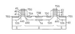
FIG. 5 , each single gate electro-static discharge element M1 of the ESD-protection-driver circuit 30 includes agate electrode 42 arranged on asubstrate 40 of p− silicon, which is of a second conductivity type, by way of agate oxidation film 41. The side surface of thegate electrode 42 is covered by asidewall 43 formed by a silicon oxidation film. Lightly doped drain (LDD)regions substrate 40 with thegate electrode 42 located therebetween. TheLDD regions substrate 40 at a source formation region S and a drain formation region D. An n+ diffusion region45S is formed on the inner side of eachLDD region 44S. An n+ diffusion region45D is formed at the inner side of theLDD region 44D. - A
source electrode 50 and adrain electrode 51 including silicide layers are formed in the surfaces of the n+ diffusion regions45S and45D at the outer side of thesidewall 43. Thesource electrode 50 is formed in the entire exposed surface of the n+ diffusion region45S that is adjacent to thesidewall 43. Thedrain electrode 51 is formed in the surface of the n+ diffusion region45D spaced apart from thesidewall 43 of eachgate electrode 42. Asilicide block region 52, which does not include a silicide layer, is formed between thedrain electrode 51 and thesidewall 43. Thesilicide block region 52 serves as the ballast resistor R. - A p+ diffusion region55 is formed immediately below the
drain electrode 51 in the lower part of the n+ diffusion region45D of the drain formation region D. As shown inFIG. 6 , the p+ diffusion region55 is formed to be as wide as possible in the drain formation region D at a region excluding the lower side of thesidewall 43 and the lower side of thesilicide block region 52. In the illustrated example, the p+ diffusion region55 and thedrain electrode 51 have substantially the same shapes and dimensions in the lateral direction. That is, the p+ diffusion region55 is aligned with thedrain electrode 51. As shown inFIG. 5 , the formation depth of the p+ diffusion region55 is controlled so that the upper part of the p+ diffusion region55 overlaps the lower part of the n+ diffusion region45D. Thus, the pn junction surface of the n+ diffusion region45D and the p+ diffusion region55 exists at a relatively shallow position that is closer to the surface of thesubstrate 40 than before formation of the p+ diffusion region55. The p+ diffusion region55 has an impurity concentration controlled to be higher than that of thesubstrate 40, more specifically, below thegate electrode 42 at the same depth. Therefore, a depletion layer formed in the pn junction surface of the n+ diffusion region45D and the p+ diffusion region55 is narrower than the depletion layer in the pn junction surface of the n+ diffusion region45D and the p− diffusion region of thesubstrate 40. - The
drain electrode 51 of each transistor T1 is coupled to metal wiring W1 through contact holes H1 (seeFIG. 6 ), and the metal wiring W1 is coupled to the input/output pad 10. The source electrode50 of each transistor T1 is coupled to metal wiring W2 through contact holes H2 (seeFIG. 6 ). The ground potential Vss is applied to the metal wiring W2. As shown inFIG. 6 , thegate electrode 42 of each transistor T1 is coupled to metal wiring W3 through a contact hole H3. The gate voltage Vg is applied to thegate electrode 42 via the metal wiring W3. The wiring of the gate voltage Vg may be coupled to the wiring of the ground potential Vss or the output terminal of the pre-buffer. - The operation of the
semiconductor device 1 will now be discussed with reference toFIG. 5 . - When ESD surge is applied to the input/
output pad 10 of thesemiconductor device 1 due to electro-static discharge and the like, the potential at then+ diffusion region 45D of the transistor T1 rises, avalanche breakdown occurs at the pn junction surface of then+ diffusion region 45D and thep+ diffusion region 55, and a pair of electron holes are formed in the pn junction surface. The holes move into thesubstrate 40 and generating a hole current Ibh2. The hole current Ibh2 raises the substrate potential. As a result, a parasitic bipolar transistor Tp1 including the p− diffusion region in thesubstrate 40, the n+ diffusion region45S, and the n+ diffusion region45D becomes electrically conductive. Since the narrow depletion layer is formed at the pn junction surface of then+ diffusion region 45D and the p+ diffusion region55, avalanche breakdown occurs due to low voltage. Therefore, the parasitic bipolar transistor Tp1 becomes electrically conductive at a low voltage. When the parasitic bipolar transistor Tp1 becomes electrically conductive, a large current (arrow C ofFIG. 5 ) flows between the n+ diffusion region45D and then+ diffusion region 45S. Thus, the ESD surge applied to the input/output pad 10 is released into the wiring of the ground potential Vss to prevent the ESD surge from being applied to theinternal circuit 20. - The ESD characteristics of the
semiconductor device 1 will now be discussed. In a state in which the gate length L (seeFIG. 6 ) was 0.36 μm and the gate width W (seeFIG. 6 ) was 360 μm, the withstanding voltage was 280V before the injection of boron ions in a machine model (MM) test. The inventors have found that the withstanding voltage in the MM test improves to 360V by injecting boron ions with an energy of 60 keV while controlling the dose amount to be 3×1013cm−2. - A process for manufacturing the
semiconductor device 1 will now be described with reference toFIG. 7 . - First, referring to
FIG. 7( a), shallow trench isolation (STI) is performed to form an electron isolation insulating film (not shown). Then, the surface of thesubstrate 40 is thermally oxidized to form thegate oxidation film 41 at a thickness of for example 8 nm. Subsequently, chemical vapor deposition (CVD) is performed to form a polycrystalline silicon film on the entire surface of thesubstrate 40. Photolithography and etching are then performed to pattern the polycrystalline silicon film and form thegate electrode 42. - Referring to
FIG. 7( b), theLDD regions gate electrode 42 as a mask. Subsequently, CVD is performed to form a silicon oxidation film so that the entire surface has a thickness of about 130 nm, and anisotropic etching is performed on the silicon oxidation film to form thesidewall 43 of eachgate electrode 42. The n+ diffusion regions45S and45D are respectively formed in the source formation region S and the drain formation region D by injecting the phosphate ions (P+) with an energy of 15 keV while controlling the dose amount at 7×1015cm−2using thegate electrode 42 and thesidewall 43 as a mask. - Referring to
FIG. 7( c), after performing photolithography to form a film of photoresist P1 on the entire surface, the photoresist P1 is patterned to a predetermined shape. The p+ diffusion region55 is formed at the lower part of the exposed n+ diffusion region45D by injecting boron ions (B+) with an energy of 60 keV while controlling the dose amount to 3×1013cm−2using the photoresist P1 patterned to the predetermined shape as a mask. In this case, the p+ diffusion region55 is formed to overlap the lower end of the above-lying n+ diffusion region45D in the depthwise direction. After ion injection, the photoresist P1 is removed, and the impurities injected into thesubstrate 40 are activated by performing rapid thermal annealing (RTA) at 1000° C. for about 10 seconds in a nitrogen atmosphere. - The injection of boron ions is preferably performed in a state in which a photoresist for covering the
internal circuit 20 of thesemiconductor device 1 is formed. This prevents an increase in the junction capacitance of the transistor (not shown) in theinternal circuit 20 of thesemiconductor device 1. - As shown in
FIG. 7( d), after performing CVD to form a silicon oxidation film on the entire surface, photolithography and etching is performed to pattern the silicon oxidation film and form an oxidation film P2 serving as a silicide block that covers part of the n+ diffusion region45D and thegate electrode 42. A silicide layer is then formed on the surface of the n+ diffusion regions45S and45D that does not include the oxidation film P2. The silicide layer formed in the surface n+ diffusion region45S of the formed silicide layer serves as thesource electrode 50, and the silicide layer formed on the surface of the n+ diffusion region45D at the upper region of the p+ diffusion region55 serves as thedrain electrode 51. The contact holes H1 (seeFIG. 6) are formed in the upper surface of thedrain electrode 51, and thedrain electrode 51 is coupled to the input/output pad 10 by the metal wiring W1 formed in the contact hole H1. The contact holes H2 (seeFIG. 6 ) are formed in the upper surface of thesource electrode 50, and thesource electrode 50 is coupled to the wiring of the ground potential Vss by the metal wiring W2 formed in the contact holes H2. - The n+ diffusion regions45S and45D in the present embodiment may be omitted. In such a case, the p+ diffusion region55 is preferably formed immediately below the
drain electrode 51 to contact the n− diffusion region44D. - The source electrode50 may be omitted. In such a case, the pattern of the oxidation film P2 must be modified so as to cover the n− diffusion region44S of the source formation region S.
- The present embodiment has the advantages described below.
- (1) The p+ diffusion region55 is formed to overlap the lower part of the n+ diffusion region45D of the drain formation region D in the depthwise direction immediately below the
drain electrode 51. Accordingly, the concentration gradient of then+ diffusion region 45D formed at the lower part of thesilicide block region 52 does not vary. This prevents the resistance of the ballast resistor R from varying in an optimal manner. As a result, the AC characteristics of the single gate electro-static discharge element (single gate electro-static discharge protection circuit/drive circuit) M1 are not varied. Thus, circuit simulation does not need to be performed again after the injection of boron ions. This reduces the development cost and the development time compared to the semiconductor device of the prior art. - (2) The patterns of the photoresist P1 and the oxidation film P2 are set so that the p+ diffusion region55 is formed only immediately below the
drain electrode 51 and as wide as possible immediately below thedrain electrode 51. Generally, the diffusion of impure ions in the lateral direction from the edges of the mask increases as the distance of the ion range becomes longer during the injection of impure ions. Accordingly, in the present embodiment, the photoresist P1 for forming the p+ diffusion region55 is applied so that the exposed portion of the drain formation region D is narrower than the oxidation film P2 for forming thedrain electrode 51, as shown inFIG. 7( d), while taking into consideration the diffusion of boron ions in the lateral direction. Therefore, the p+ diffusion region55 does not enter the region immediately below thesilicide block region 52 more than necessary even if boron ions are diffused in the lateral direction. As a result, the p+ diffusion region55 and thedrain electrode 51 are formed immediately below thedrain electrode 51 with substantially the same shapes and dimensions in the lateral direction. Furthermore, the p+ diffusion region55 is formed as wide as possible immediately below thedrain electrode 51. Thus, the hole current Ibh2 shown inFIG. 5 is supplied to thesubstrate 40 with a low voltage. Consequently, the voltage for starting the operation of the parasitic bipolar transistor Tp1 becomes further lower. FIG. 8 shows a method for manufacturing a semiconductor device including an ESD-protection-driver circuit 60 according to a second embodiment of the present invention. To avoid redundancy, like or same reference numerals are given to those components that are the same as the corresponding components shown inFIGS. 4 to 7 . Such components will not be described in detail.- As shown in
FIG. 8( a),gate electrodes 42 are formed on the surface of asubstrate 40 by way ofgate oxidation films 41. N-type diffusion regions gate electrodes 42 as masks. - Subsequently, as shown in
FIG. 8( b), CVD is performed to apply aninsulation film 62, which is formed by a silicon oxidation film, on the entire surface of thesubstrate 40. A photoresist P3 is formed on theinsulation film 62, and theinsulation film 62 is patterned using the photoresist P3 as a mask to forminsulation films FIG. 8( c). Theinsulation films type diffusion regions 61S of the source formation region S at a portion spaced apart from thegate electrodes 42 by a distance corresponding to the sidewalls. Further, the n-type diffusion region 61D of the drain formation region D is exposed at a portion spaced apart from thegate electrodes 42 by a distance corresponding to the sidewalls and the silicide block. Then, p+ diffusion regions63S and63D are respectively formed in the exposed portions of the source formation region S and the drain formation region D by injecting boron ions with an energy of 10 keV while controlling the dose amount to be 1×1013cm−2using theinsulation films insulation films substrate 40 by injecting arsenic ions with an energy of 5 keV while controlling the dose amount to be 2×1014cm−2. The p+ diffusion regions63S and63D and the n+ diffusion regions64S and64D are formed so as to be overlapped in the depthwise direction and so that a significantly narrow depletion layer is formed in the pn junction surface of the p+ diffusion regions63S and63D and the n+ diffusion regions64S and64D. Subsequently, RTA is performed to activate the impurities injected into thesubstrate 40. - Referring to
FIG. 8( d), continuously using theinsulation films source electrode 66S and adrain electrode 66D formed by silicide layers are respectively formed in the surfaces of the exposed source formation region S and the drain formation region D. Theinsulation films region 67 serves as a silicide block. The silicide block is one type of ballast resistor. - The ESD-protection-
driver circuit 60 is configured by coupling thedrain electrode 66D to the input/output pad 10 and coupling thesource electrode 66S to the wiring of the ground potential Vss. The coupling of the gate electrode will not be described here. - In the present embodiment, the n+ diffusion regions65S and65D are formed before the formation of the silicide layer. However, the formation of the n+ diffusion regions65S and65D may be omitted. The n+ diffusion region64S, the p+ diffusion region63S, and the
source electrode 66S, which are formed in the source formation region S, in the present embodiment may be omitted. In this case, the pattern of the photoresist P3 used for patterning theinsulation film 62 inFIG. 8( b) must be modified to cover theinsulation film 62 formed on the source formation region S. The insulation film for covering the source formation region S is formed by performing patterning using the modified photoresist P3. - The present embodiment has the advantages described below.
- (1) In the same manner as in the first embodiment, an avalanche breakdown occurs due to low voltage at the pn junction surface of the n+ diffusion region64D and the p+ diffusion region63D formed immediately below the
drain electrode 66D. Thus, the voltage for starting operation of the parasitic bipolar transistor Tp1 becomes lower compared to thesemiconductor device 100 of the prior art. Furthermore, the n+ diffusion region64D is formed at a significantly shallow portion in the surface of thesubstrate 40. This causes an avalanche breakdown more effectively than thesemiconductor device 1 of the first embodiment. - (2) The
insulation films drain electrode 66D. The diffusion of boron ions in the lateral direction during ion injection forms the p+ diffusion region63D in some portions immediately below thesilicide block region 67. However, the p+ diffusion region63D is very narrow. This prevents the resistance of the ballast resistor R from varying in a more optimal manner than the single gate electro-static discharge element M10 of the prior art. Theinsulation films source electrode 66S, and thedrain electrode 66D. This significantly reduces the number of manufacturing steps. Furthermore, since theinsulation films gate electrodes 42 and thesilicide block region 67, there is no need for a separate step for forming a sidewall on the side surface of thegate electrode 42. FIG. 9 shows a method for manufacturing a semiconductor device including an ESD-protection-driver circuit 70 according to a third embodiment of the present invention. To avoid redundancy, like or same reference numerals are given to those components that are the same as the corresponding components shown inFIGS. 4 to 8 . Such components will not be described in detail.- Referring to
FIG. 9( a),gate electrodes 42 are formed on the surface of asubstrate 40 by way ofgate oxidation films 41. Further,LDD regions gate electrodes 42 as masks.Sidewalls 43 are then formed on thegate electrodes 42. - Referring to
FIG. 9( b), after performing photolithography to form a film of photoresist over the entire surface, the photoresist is patterned to a predetermined shape to form two photoresists P4 and P5 on the surface of the drain formation region D. The photoresists P4 and P5 are spaced apart from thesidewall 43 of eachgate electrode 42. Further, the photoresists P4 and P5 are spaced apart from each other. Due to the photoresists P4 and P5, the source formation region S is exposed at a portion spaced apart from thegate electrode 42 by a distance corresponding to thesidewall 43, and three spaced exposedportions portions 71A to71C by injecting phosphor ions with an energy of 15 keV while controlling the dose amount to be 7×1015cm−2using the photoresists P4 and P5, thegate electrodes 42, and thesidewalls 43 as masks. After performing ion injection, the photoresists P4 and P5 are removed, and the impurities injected into thesubstrate 40 are activated by performing rapid thermal annealing (RTA) at 1000° C. for about ten seconds in a nitrogen atmosphere. - Referring to
FIG. 9( c), after performing photolithography to form a film of photoresist over the entire surface, the photoresist is patterned to a predetermined shape to form photoresist P6 exposing only the exposedportion 71B of the drain formation region D. A p+ diffusion region74 is formed at the lower part of the n+ diffusion region72B by injecting boron ions with an energy of 60 keV while controlling the dose amount to be 3×1013cm−2using the photoresist P6 as a mask. In this case, the p+ diffusion region74 is formed to partially overlap the overlying n+ diffusion region72B in the depthwise direction. A very narrow depletion layer is formed at the pn junction surface in the n+ diffusion region72B and the p+ diffusion region74. After performing ion injection, the photoresist P6 is removed, and the impurities injected into thesubstrate 40 are activated by performing rapid thermal annealing (RTA) at 1000° C. for about ten seconds in a nitrogen atmosphere. - As shown in
FIG. 9( d), after performing CVD to form a silicon oxidation film over the entire surface, photolithography and etching are performed to pattern the silicon oxidation film is patterned to form oxidation films P7 and P8 shaped identically to the photoresists P4 and P5 shown inFIG. 9( b). Silicide layers75G,75S,75A,75B, and75C are then formed on the surfaces of thegate electrodes 42 and in the surfaces of thesubstrate 40 at the exposed source formation region S and the exposedportions silicide layer 75B formed above the p+ diffusion region74 is coupled to the input/output pad 10. That is, thesilicide layer 75B formed in the exposedportion 71B serves as the drain electrode. Thesilicide layer 75S formed in the source formation region S is coupled to the wiring of the ground potential Vss. This forms the ESD-protection-driver circuit 70. - The present embodiment has the advantages described below.
- (1) In the same manner as the first and second embodiments, an avalanche breakdown occurs due to low voltage at the pn junction surface of the n+ diffusion region72B and the p+ diffusion region74 formed immediately below the
silicide layer 75B, which serves as the drain electrode. This lowers the voltage for starting operation of the parasitic bipolar transistor Tp1 compared to thesemiconductor device 100 of the prior art. - (2) The patterns of the photoresist P6 and the oxidation films P7 and P8 are set so that the p+ diffusion region74 is formed only immediately below the
silicide layer 75B serving as the drain electrode as wide as possible immediately below thesilicide layer 75B. That is, the patterns of the photoresist P6 and the oxidation films P7 and P8 are set to form the p+ diffusion region74 with substantially the same shape and dimensions in the lateral direction as thesilicide layer 75B immediately below thesilicide layer 75B. This obtains the same advantages as the first embodiment. - A
semiconductor device 80 including an ESD-protection-driver circuit 90 according to a fourth embodiment of the present invention will now be described with reference toFIGS. 10 to 12 . To avoid redundancy, like or same reference numerals are given to those components that are the same as the corresponding components shown inFIGS. 4 to 9 . Such components will not be described in detail. - As shown in
FIG. 10 , thesemiconductor device 80 includes an input/output pad 10, aninternal circuit 20, and an ESD-protection-driver circuit 90 coupled to a node between the input/output pad 10 and theinternal circuit 20. The ESD-protection-driver circuit 90 includes a plurality of cascade coupled electro-static discharge elements M2, which are coupled to one another in parallel. In each cascade coupled electro-static discharge element M2, an N-channel MOS transistor T1A and an N-channel MOS transistor T1B are coupled in series, and the N-channel MOS transistors and a ballast resistor R are coupled in series. - When using the cascade coupled electro-static discharge element M2 for two types of input/output signal voltages, for example, 3.3 V and 5 V, two transistors are normally designed in correspondence with the low input/output signal voltage (e.g., 3.3 V). During use, the gate voltage Vg1 (3.3 V), which is close to the low input/output signal voltage, is applied to the gate of the transistor T1A coupled to the input/output pad. The gate of the transistor T1B of which source is coupled to the wiring of the ground potential Vss may be coupled to the wiring of the ground potential Vss or the output terminal of a pre-buffer. In such a configuration, the gate voltage Vg1 of the transistor T1A is 3.3 V even if a signal voltage of 5.0 V is applied to the input/
output pad 10. Thus, the drain-gate voltage is 1.7 V and low, and the gate oxidation film of the transistor T1A will not be damaged. Therefore, the cascade coupled electro-static discharge element M2 is applicable to two types of input/output signal voltages, 3.3 V and 5.0 V. - As shown in
FIG. 11 , the ESD-protection-driver circuit 90 includes afirst gate electrode 92A of the transistor T1A and asecond gate electrode 92B of the transistor T1B arranged on thesubstrate 40 by way ofgate oxidation films 91. Asilicide layer 96G is formed on the surfaces of the first andsecond gate electrodes 92A and29B. Asidewall 93 is formed on each side surface of the first andsecond gate electrodes LDD regions substrate 40 so that the first andsecond gate electrodes LDD regions substrate 40. Further, n+ diffusion regions95S,95N, and95D are respectively formed at the inner side of theLDD region 94S, the inner side of theLDD region 94N, and the inner side of theLDD region 94D. The n+ diffusion region95N of the node formation region N serves as a node E (seeFIG. 10 ) between the transistors T1A and T1B and as the drain region of the transistor T1A and the source region of the transistor T1B. - A
source electrode 96S, asilicide layer 96N, and adrain electrode 96D are respectively formed in the surfaces of the n+ diffusion regions95S,95N, and95D entirely or partially at portions where thesidewalls 93 are not formed. Specifically, thesource electrode 96S is formed in the entire exposed surface of the n+ diffusion region95S in the source formation region S adjacent to thesidewall 93 of thesecond gate electrode 92B. Thesilicide layer 96N is formed on the entire exposed surface of the n+ diffusion region95N in the node formation region N between thesidewalls 93 of thegate electrodes drain electrode 96D is formed at a local region in the surface of the n+ diffusion region95D spaced apart from thesidewall 93 of thefirst gate electrode 92A. Asilicide block region 97 is formed between thedrain electrode 96D and thesidewall 93 where a silicide layer is not formed. Thesilicide block region 97 serves as the ballast resistor R. - Further, a p+ diffusion region98 is formed at the lower part of the n+ diffusion region95D in the drain formation region D in the region immediately below the
drain electrode 96D. As shown inFIG. 12 , the p+ diffusion region98 is formed as wide as possible in the drain formation region D at portions excluding thesidewall 93 and thesilicide block region 97. In the illustrated example, the p+ diffusion region98 and thedrain electrode 96D have substantially the same shapes and dimensions in the lateral direction. In other words, the p+ diffusion region98 is aligned with thedrain electrode 96D. As shown inFIG. 11 , the p+ diffusion region98 is formed so as to overlap the lower part of the n+ diffusion region95D in the depthwise direction. The p+ diffusion region98 has an impurity concentration that is controlled to be higher than that of thesubstrate 40. Therefore, a depletion layer narrower than the depletion layer at the pn junction surface of the n+ diffusion region95D and the p− diffusion region of thesubstrate 40 is formed in the pn junction surface of the n+ diffusion region95D and the p+ diffusion region98. - Metal wiring W1 is coupled to the
drain electrode 96D of each transistor T1A through contact holes H1 (seeFIG. 12 ), and the metal wiring W1 is coupled to the input/output pad 10. Metal wiring W2 is coupled to thesource electrode 96S of each transistor T1B through contact holes H2 (seeFIG. 12 ), and the ground potential Vss is applied to the metal wiring W2. As shown inFIG. 12 , thefirst gate electrode 92A of each transistor T1A is coupled to metal wiring W4 through a contact hole H4, and the gate voltage Vg1 is applied to thefirst gate electrode 92A via the metal wiring W4. The gate voltage Vg1 is set to, for example, 3.3 V during normal operation. Thesecond gate electrode 92B of each transistor T1B is coupled to metal wiring W5 through a contact hole H5, and the gate voltage Vg2 is applied to thesecond gate electrode 92B via metal wiring W5. Thesecond gate electrode 92B of each transistor T1B may be coupled to the wiring of the ground potential Vss or the output terminal of the pre-buffer during normal operation. - The operation of the
semiconductor device 80 will now be described. - When an ESD surge is applied to the input/
output pad 10 of thesemiconductor device 80 due to electro-static discharge or the like, an avalanche breakdown occurs at the pn junction surface of the n− diffusion region94D and the p− diffusion region of thesubstrate 40 and at the pn junction surface of the n+ diffusion region95D and the p+ diffusion region98. Further, a hole current Ibh2 is supplied to thesubstrate 40. As a result, a parasitic bipolar transistor Tp2 including the p− diffusion region of thesubstrate 40, the n+ diffusion region95D of the first transistor T1A, and the n+ diffusion region95S of the second transistor T1B becomes electrically conductive. Since a narrow depletion layer is formed in the pn junction surface of the n+ diffusion region95D and the p+ diffusion region98, an avalanche breakdown occurs due to low voltage. Accordingly, the parasitic bipolar transistor Tp2 also becomes electrically conductive at a low voltage. When the parasitic bipolar transistor Tp2 becomes electrically conductive, a large current flows between the n+ diffusion region95D and the n+ diffusion region95S. This releases the ESD surge applied to the input/output pad 10 to the wiring of the ground potential Vss and prevents ESD surge from being applied to theinternal circuit 20. - In the
semiconductor device 80, with regard to the ESD resistance characteristics when the base length Lb (seeFIG. 12 ) of the parasitic bipolar transistor Tp2 is 0.97 μm approximately and the gate width W (seeFIG. 12 ) is 360 μm, the withstanding voltage was 120 V in a machine mode (MM) test before the injection of boron ions. The inventors found that the withstanding voltage improves to 280 V in the MM test by injecting boron ions with an energy of 60 keV while controlling the dose amount to be 3×1013cm−2. The inventors also found that the withstanding voltage of 2600 V in a human body model (HBM) before injection of boron ions greatly improves the withstanding voltage to be 4000 V or higher in an HBM test after ion injection. The parasitic bipolar transistor Tp2 is configured by the p− diffusion region in thesubstrate 40, the n+ diffusion region95D of the first transistor T1A, and the n+ diffusion region95S of the second transistor T1B. Thus, the base length Lb becomes equal to the total value of the gate length of 0.36 μm of the first andsecond gate electrodes - A method for manufacturing the
semiconductor device 80 will now be discussed with reference toFIG. 13 . - First, referring to
FIG. 13( a), thefirst gate electrode 92A andsecond gate electrode 92B are formed spaced apart from each other on the surface of thesubstrate 40 by way of thegate oxidation films 91. TheLDD regions first-gate electrode 92A and thesecond gate electrode 92B as a mask. Then, CVD is performed to form a silicon oxidation film having a thickness of about 130 nm on the entire surface. Then, anisotropic etching is performed on the silicon oxidation film to form thesidewall 93 of eachgate electrode gate electrodes sidewall 93 as a mask. - Referring to
FIG. 13( b), after performing photolithography to form a film of photoresist over the entire surface, the photoresist is patterned to a predetermined shape to form a photoresist P9 exposing only part of the drain formation region D. The p+ diffusion region98 is formed at the lower part of the n+ diffusion region95D in the exposed drain formation region D by injecting boron ions (B+) with an energy of 60 keV while controlling the dose amount to be 3×1013cm−2using the photoresist P9 as the mask. In this case, the p+ diffusion region98 is formed to overlap the lower end of the overlying n+ diffusion region95D in the depthwise direction. After ion injection, the photoresist P9 is removed, and impurities are injected into thesubstrate 40 and activated by performing RTA at 1000° C. for about ten seconds in a nitrogen atmosphere. - Referring to
FIG. 13( c), after performing CVD to form a silicon oxidation film over the entire surface, photolithography and etching are performed to pattern the silicon oxidation film and form an oxidation film P10 serving as a silicide block for covering part of the n+ diffusion region95D adjacent to thesidewall 93 of thefirst gate electrode 92A. A silicide layer is then formed on eachgate electrode source electrode 96S, and the silicide layer formed on the surface of the n+ diffusion region95D at the upper region of the p+ diffusion region98 serves as thedrain electrode 96D. The contact holes H1 (seeFIG. 12) are formed in the upper surface of thedrain electrode 96D, and thedrain electrode 96D is coupled to the input/output pad 10 by the metal wiring W1 (seeFIG. 11 ) formed in the contact holes H1. The contact holes H2 (seeFIG. 12 ) are formed in the upper surface of thesource electrode 96S, and thesource electrode 96S is coupled to the wiring of the ground potential Vss by the metal wiring W2 (seeFIG. 12 ) formed in the contact hole H2. This forms the ESD-protection-driver circuit 70. - The present embodiment has the advantages described below.
- (1) An avalanche breakdown occurs due to low voltage at the pn junction surface of the
n+ diffusion region 95D and thep+ diffusion region 98 formed immediately below thedrain electrode 96D. Thus, the voltage for starting operation of the parasitic bipolar transistor Tp2 becomes low. - (2) The patterns of the photoresist P9 and the oxidation film P10 are set so as to form the p+ diffusion region98 only immediately below the
drain electrode 96D and as wide as possible. In the illustrated example, the patterns of the photoresist P9 and the oxidation film P10 are set so as to form the p+ diffusion region98 immediately below thedrain electrode 96D so that the p+ diffusion region98 and thedrain electrode 96D have substantially the same shapes and dimensions in the lateral direction. Therefore, the same advantages as the first embodiment are obtained. - It should be apparent to those skilled in the art that the present invention may be embodied in many other specific forms without departing from the spirit or scope of the invention.
- The shapes of the silicide block region and the drain electrode are not particularly limited. For example, the shape may be changed as shown in
FIG. 14 .FIG. 14 shows a modification of the third embodiment shown inFIG. 9 . Specifically, the three n+ diffusion regions72A,72B, and72C formed in the drain formation region D shown inFIG. 9 may be modified to a single n+ diffusion region72D. - The formation of the n+ diffusion region in the drain formation region D in the first, third, and fourth embodiments may be omitted. In such cases, the p+ diffusion region may be formed immediately below the drain electrode to contact the lower end of the n− diffusion region. Further, a new n+ diffusion region may be formed under the p+ diffusion region.
- In the first, third, and fourth embodiments, the p+ diffusion regions55,74,98 may be formed by injecting boron ions before forming the n+ diffusion regions45D,72B,95D.
- In the second embodiment, the
insulation films gate electrode 42 and theside block region 67. However, the sidewalls of thegate electrode 42 and theside block region 67 may be formed separately. In such a case, it is preferred that photolithography be performed to pattern photoresist and form a mask for forming the p+ diffusion region63D. - The silicide layer may be formed on the surface of the
gate electrode 42 in the first and second embodiments. In such a case, the pattern of the oxidation film P2 must be modified to expose thegate electrode 42. - In the step of
FIG. 9( d) in the third embodiment, the silicide layer may be formed separately from the oxidation film for covering thegate electrode 42. Further, the silicide layer may be formed separately from the oxidation film for covering the n− diffusion region75S of the source formation region S. - In the step of
FIG. 13( c) in the fourth embodiment, the pattern of the oxidation film P10 may be modified to cover the first andsecond gate electrodes - In the above embodiments, boron ions are injected to form the p+ diffusion region. However, the present invention is not limited in such a manner as long as p-type impure ions are used.
- In the above embodiments, the transistors T1, T1A, T1B are N-channel MOS transistors but may be changed to P-channel MOS transistors.
- The present examples and embodiments are to be considered as illustrative and not restrictive, and the invention is not to be limited to the details given herein, but may be modified within the scope and equivalence of the appended claims.
Claims (20)
Priority Applications (1)
| Application Number | Priority Date | Filing Date | Title |
|---|---|---|---|
| US13/715,773US8722522B2 (en) | 2007-02-20 | 2012-12-14 | Electro-static discharge protection device, semiconductor device, and method for manufacturing electro-static discharge protection device |
Applications Claiming Priority (2)
| Application Number | Priority Date | Filing Date | Title |
|---|---|---|---|
| JP2007-039703 | 2007-02-20 | ||
| JP2007039703AJP5217180B2 (en) | 2007-02-20 | 2007-02-20 | Method for manufacturing electrostatic discharge protection device |
Related Child Applications (1)
| Application Number | Title | Priority Date | Filing Date |
|---|---|---|---|
| US13/715,773DivisionUS8722522B2 (en) | 2007-02-20 | 2012-12-14 | Electro-static discharge protection device, semiconductor device, and method for manufacturing electro-static discharge protection device |
Publications (2)
| Publication Number | Publication Date |
|---|---|
| US20080211028A1true US20080211028A1 (en) | 2008-09-04 |
| US8354723B2 US8354723B2 (en) | 2013-01-15 |
Family
ID=39732462
Family Applications (2)
| Application Number | Title | Priority Date | Filing Date |
|---|---|---|---|
| US12/034,173Active2029-02-05US8354723B2 (en) | 2007-02-20 | 2008-02-20 | Electro-static discharge protection device, semiconductor device, and method for manufacturing electro-static discharge protection device |
| US13/715,773ActiveUS8722522B2 (en) | 2007-02-20 | 2012-12-14 | Electro-static discharge protection device, semiconductor device, and method for manufacturing electro-static discharge protection device |
Family Applications After (1)
| Application Number | Title | Priority Date | Filing Date |
|---|---|---|---|
| US13/715,773ActiveUS8722522B2 (en) | 2007-02-20 | 2012-12-14 | Electro-static discharge protection device, semiconductor device, and method for manufacturing electro-static discharge protection device |
Country Status (4)
| Country | Link |
|---|---|
| US (2) | US8354723B2 (en) |
| JP (1) | JP5217180B2 (en) |
| KR (1) | KR100994436B1 (en) |
| TW (1) | TWI364835B (en) |
Cited By (28)
| Publication number | Priority date | Publication date | Assignee | Title |
|---|---|---|---|---|
| US20100187627A1 (en)* | 2008-03-13 | 2010-07-29 | Tela Innovations, Inc. | Channelized Gate Level Cross-Coupled Transistor Device with Overlapping PMOS Transistors and Overlapping NMOS Transistors Relative to Direction of Gate Electrodes |
| CN101800246A (en)* | 2010-03-12 | 2010-08-11 | 上海宏力半导体制造有限公司 | ESD device |
| US20110215404A1 (en)* | 2010-03-08 | 2011-09-08 | Taiwan Semiconductor Manufacturing Company, Ltd. | Method and Apparatus of Forming ESD Protection Device |
| US20130001704A1 (en)* | 2011-06-28 | 2013-01-03 | Taiwan Semiconductor Manufacturing Company., Ltd. | Resistors Formed Based on Metal-Oxide-Semiconductor Structures |
| US20130001686A1 (en)* | 2011-07-01 | 2013-01-03 | Magnachip Semiconductor, Ltd. | Electro-static discharge protection device |
| US8541879B2 (en) | 2007-12-13 | 2013-09-24 | Tela Innovations, Inc. | Super-self-aligned contacts and method for making the same |
| US8549455B2 (en) | 2007-08-02 | 2013-10-01 | Tela Innovations, Inc. | Methods for cell phasing and placement in dynamic array architecture and implementation of the same |
| US8653857B2 (en) | 2006-03-09 | 2014-02-18 | Tela Innovations, Inc. | Circuitry and layouts for XOR and XNOR logic |
| US8658542B2 (en) | 2006-03-09 | 2014-02-25 | Tela Innovations, Inc. | Coarse grid design methods and structures |
| US8661392B2 (en) | 2009-10-13 | 2014-02-25 | Tela Innovations, Inc. | Methods for cell boundary encroachment and layouts implementing the Same |
| US8667443B2 (en) | 2007-03-05 | 2014-03-04 | Tela Innovations, Inc. | Integrated circuit cell library for multiple patterning |
| US8680626B2 (en) | 2007-10-26 | 2014-03-25 | Tela Innovations, Inc. | Methods, structures, and designs for self-aligning local interconnects used in integrated circuits |
| US8701071B2 (en) | 2008-01-31 | 2014-04-15 | Tela Innovations, Inc. | Enforcement of semiconductor structure regularity for localized transistors and interconnect |
| US8756551B2 (en) | 2007-08-02 | 2014-06-17 | Tela Innovations, Inc. | Methods for designing semiconductor device with dynamic array section |
| US8759985B2 (en) | 2008-03-27 | 2014-06-24 | Tela Innovations, Inc. | Methods for multi-wire routing and apparatus implementing same |
| US8823062B2 (en) | 2006-03-09 | 2014-09-02 | Tela Innovations, Inc. | Integrated circuit with offset line end spacings in linear gate electrode level |
| US8839175B2 (en) | 2006-03-09 | 2014-09-16 | Tela Innovations, Inc. | Scalable meta-data objects |
| US8863063B2 (en) | 2009-05-06 | 2014-10-14 | Tela Innovations, Inc. | Finfet transistor circuit |
| US9035359B2 (en) | 2006-03-09 | 2015-05-19 | Tela Innovations, Inc. | Semiconductor chip including region including linear-shaped conductive structures forming gate electrodes and having electrical connection areas arranged relative to inner region between transistors of different types and associated methods |
| US9122832B2 (en) | 2008-08-01 | 2015-09-01 | Tela Innovations, Inc. | Methods for controlling microloading variation in semiconductor wafer layout and fabrication |
| US9159627B2 (en) | 2010-11-12 | 2015-10-13 | Tela Innovations, Inc. | Methods for linewidth modification and apparatus implementing the same |
| US9230910B2 (en) | 2006-03-09 | 2016-01-05 | Tela Innovations, Inc. | Oversized contacts and vias in layout defined by linearly constrained topology |
| US9563733B2 (en) | 2009-05-06 | 2017-02-07 | Tela Innovations, Inc. | Cell circuit and layout with linear finfet structures |
| CN107017249A (en)* | 2017-03-30 | 2017-08-04 | 北京中电华大电子设计有限责任公司 | It is a kind of to improve the method for ESD protective device uniform conducting |
| US9754878B2 (en) | 2006-03-09 | 2017-09-05 | Tela Innovations, Inc. | Semiconductor chip including a chip level based on a layout that includes both regular and irregular wires |
| US10573643B2 (en)* | 2016-12-15 | 2020-02-25 | Samsung Electronics Co., Ltd. | Integrated circuit having vertical transistor and semiconductor device including the integrated circuit |
| US11430749B2 (en)* | 2018-10-31 | 2022-08-30 | Infineon Technologies Ag | ESD protection in an electronic device |
| US20220320071A1 (en)* | 2019-12-18 | 2022-10-06 | Taiwan Semiconductor Manufacturing Company, Ltd. | Semiconductor device having improved electrostatic discharge protection |
Families Citing this family (2)
| Publication number | Priority date | Publication date | Assignee | Title |
|---|---|---|---|---|
| KR100974599B1 (en) | 2008-08-07 | 2010-08-06 | 현대자동차주식회사 | Urea injection quantity control device and method of vehicle |
| JP2014225483A (en)* | 2011-09-16 | 2014-12-04 | パナソニック株式会社 | Semiconductor integrated circuit device |
Citations (19)
| Publication number | Priority date | Publication date | Assignee | Title |
|---|---|---|---|---|
| US5493142A (en)* | 1994-01-12 | 1996-02-20 | Atmel Corporation | Input/output transistors with optimized ESD protection |
| US5498887A (en)* | 1993-01-12 | 1996-03-12 | Sony Corporation | Output circuit device for a charge transfer element having tripartite diffusion layer |
| US5559352A (en)* | 1993-10-22 | 1996-09-24 | United Microelectronics Corporation | ESD protection improvement |
| US6075271A (en)* | 1998-03-03 | 2000-06-13 | Motorola, Inc. | Semiconductor device inhibiting parasitic effects during electrostatic discharge |
| US6111267A (en)* | 1997-05-13 | 2000-08-29 | Siemens Aktiengesellschaft | CMOS integrated circuit including forming doped wells, a layer of intrinsic silicon, a stressed silicon germanium layer where germanium is between 25 and 50%, and another intrinsic silicon layer |
| US6171891B1 (en)* | 1998-02-27 | 2001-01-09 | Taiwan Semiconductor Manufacturing Company | Method of manufacture of CMOS device using additional implant regions to enhance ESD performance |
| US6265254B1 (en)* | 1996-12-13 | 2001-07-24 | Hitachi, Ltd. | Semiconductor integrated circuit devices and a method of manufacturing the same |
| US6630724B1 (en)* | 2000-08-31 | 2003-10-07 | Micron Technology, Inc. | Gate dielectric antifuse circuits and methods for operating same |
| US6835985B2 (en)* | 2000-12-07 | 2004-12-28 | Chartered Semiconductor Manufacturing Ltd. | ESD protection structure |
| US20050029601A1 (en)* | 2003-08-04 | 2005-02-10 | International Business Machines Corporation | Structure and method of making strained semiconductor cmos transistors having lattice-mismatched source and drain regions |
| US6873017B2 (en)* | 2003-05-14 | 2005-03-29 | Fairchild Semiconductor Corporation | ESD protection for semiconductor products |
| US6897536B2 (en)* | 2002-06-11 | 2005-05-24 | Fujitsu Limited | ESD protection circuit |
| US6900088B2 (en)* | 2001-03-09 | 2005-05-31 | Fujitsu Limited | Semiconductor device and its manufacture method |
| US20050266631A1 (en)* | 2004-05-26 | 2005-12-01 | Fujitsu Limited | Semiconductor device fabricating method |
| US20060001097A1 (en)* | 2004-07-01 | 2006-01-05 | Toshio Nomura | Semiconductor device and manufacturing method of the same |
| US7112495B2 (en)* | 2003-08-15 | 2006-09-26 | Taiwan Semiconductor Manufacturing Company, Ltd. | Structure and method of a strained channel transistor and a second semiconductor component in an integrated circuit |
| US20060273398A1 (en)* | 2005-06-02 | 2006-12-07 | Fujitsu Limited | Semiconductor device and manufacturing method of semiconductor device |
| US7250332B2 (en)* | 2004-08-19 | 2007-07-31 | United Microelectronics Corp. | Method for fabricating a semiconductor device having improved hot carrier immunity ability |
| US7709896B2 (en)* | 2006-03-08 | 2010-05-04 | Infineon Technologies Ag | ESD protection device and method |
Family Cites Families (7)
| Publication number | Priority date | Publication date | Assignee | Title |
|---|---|---|---|---|
| JPH06349852A (en)* | 1993-06-08 | 1994-12-22 | Fuji Electric Co Ltd | Mos type field-effect transistor |
| JP3926964B2 (en) | 1999-07-01 | 2007-06-06 | 株式会社東芝 | Semiconductor device and manufacturing method thereof |
| JP2001308297A (en)* | 2000-04-26 | 2001-11-02 | Hitachi Ltd | Semiconductor integrated circuit device and method of manufacturing the same |
| JP2002134743A (en)* | 2000-10-24 | 2002-05-10 | Matsushita Electric Ind Co Ltd | Semiconductor device and manufacturing method thereof |
| JP4794142B2 (en)* | 2004-06-18 | 2011-10-19 | 富士通セミコンダクター株式会社 | Manufacturing method of semiconductor device |
| US7119405B2 (en)* | 2005-02-11 | 2006-10-10 | Lsi Logic Corporation | Implantation method to improve ESD robustness of thick gate-oxide grounded-gate NMOSFET's in deep-submicron CMOS technologies |
| JP2007005825A (en)* | 2006-09-04 | 2007-01-11 | Fujitsu Ltd | Manufacturing method of semiconductor device |
- 2007
- 2007-02-20JPJP2007039703Apatent/JP5217180B2/ennot_activeExpired - Fee Related
- 2008
- 2008-02-20KRKR1020080015242Apatent/KR100994436B1/ennot_activeExpired - Fee Related
- 2008-02-20USUS12/034,173patent/US8354723B2/enactiveActive
- 2008-02-20TWTW097105898Apatent/TWI364835B/enactive
- 2012
- 2012-12-14USUS13/715,773patent/US8722522B2/enactiveActive
Patent Citations (22)
| Publication number | Priority date | Publication date | Assignee | Title |
|---|---|---|---|---|
| US5498887A (en)* | 1993-01-12 | 1996-03-12 | Sony Corporation | Output circuit device for a charge transfer element having tripartite diffusion layer |
| US5559352A (en)* | 1993-10-22 | 1996-09-24 | United Microelectronics Corporation | ESD protection improvement |
| US5493142A (en)* | 1994-01-12 | 1996-02-20 | Atmel Corporation | Input/output transistors with optimized ESD protection |
| US6265254B1 (en)* | 1996-12-13 | 2001-07-24 | Hitachi, Ltd. | Semiconductor integrated circuit devices and a method of manufacturing the same |
| US6111267A (en)* | 1997-05-13 | 2000-08-29 | Siemens Aktiengesellschaft | CMOS integrated circuit including forming doped wells, a layer of intrinsic silicon, a stressed silicon germanium layer where germanium is between 25 and 50%, and another intrinsic silicon layer |
| US6703663B1 (en)* | 1998-02-27 | 2004-03-09 | Taiwan Semiconductor Manufacturing Company | CMOS device using additional implant regions to enhance ESD performance and device manufactured thereby |
| US6171891B1 (en)* | 1998-02-27 | 2001-01-09 | Taiwan Semiconductor Manufacturing Company | Method of manufacture of CMOS device using additional implant regions to enhance ESD performance |
| US6075271A (en)* | 1998-03-03 | 2000-06-13 | Motorola, Inc. | Semiconductor device inhibiting parasitic effects during electrostatic discharge |
| US6630724B1 (en)* | 2000-08-31 | 2003-10-07 | Micron Technology, Inc. | Gate dielectric antifuse circuits and methods for operating same |
| US6835985B2 (en)* | 2000-12-07 | 2004-12-28 | Chartered Semiconductor Manufacturing Ltd. | ESD protection structure |
| US6900088B2 (en)* | 2001-03-09 | 2005-05-31 | Fujitsu Limited | Semiconductor device and its manufacture method |
| US6897536B2 (en)* | 2002-06-11 | 2005-05-24 | Fujitsu Limited | ESD protection circuit |
| US6873017B2 (en)* | 2003-05-14 | 2005-03-29 | Fairchild Semiconductor Corporation | ESD protection for semiconductor products |
| US20050029601A1 (en)* | 2003-08-04 | 2005-02-10 | International Business Machines Corporation | Structure and method of making strained semiconductor cmos transistors having lattice-mismatched source and drain regions |
| US6891192B2 (en)* | 2003-08-04 | 2005-05-10 | International Business Machines Corporation | Structure and method of making strained semiconductor CMOS transistors having lattice-mismatched semiconductor regions underlying source and drain regions |
| US7112495B2 (en)* | 2003-08-15 | 2006-09-26 | Taiwan Semiconductor Manufacturing Company, Ltd. | Structure and method of a strained channel transistor and a second semiconductor component in an integrated circuit |
| US20050266631A1 (en)* | 2004-05-26 | 2005-12-01 | Fujitsu Limited | Semiconductor device fabricating method |
| US20060001097A1 (en)* | 2004-07-01 | 2006-01-05 | Toshio Nomura | Semiconductor device and manufacturing method of the same |
| US7250332B2 (en)* | 2004-08-19 | 2007-07-31 | United Microelectronics Corp. | Method for fabricating a semiconductor device having improved hot carrier immunity ability |
| US20060273398A1 (en)* | 2005-06-02 | 2006-12-07 | Fujitsu Limited | Semiconductor device and manufacturing method of semiconductor device |
| US7492011B2 (en)* | 2005-06-02 | 2009-02-17 | Fujitsu Limited | Semiconductor device and manufacturing method of semiconductor device |
| US7709896B2 (en)* | 2006-03-08 | 2010-05-04 | Infineon Technologies Ag | ESD protection device and method |
Cited By (120)
| Publication number | Priority date | Publication date | Assignee | Title |
|---|---|---|---|---|
| US9754878B2 (en) | 2006-03-09 | 2017-09-05 | Tela Innovations, Inc. | Semiconductor chip including a chip level based on a layout that includes both regular and irregular wires |
| US9741719B2 (en) | 2006-03-09 | 2017-08-22 | Tela Innovations, Inc. | Methods, structures, and designs for self-aligning local interconnects used in integrated circuits |
| US8946781B2 (en) | 2006-03-09 | 2015-02-03 | Tela Innovations, Inc. | Integrated circuit including gate electrode conductive structures with different extension distances beyond contact |
| US10230377B2 (en) | 2006-03-09 | 2019-03-12 | Tela Innovations, Inc. | Circuitry and layouts for XOR and XNOR logic |
| US10217763B2 (en) | 2006-03-09 | 2019-02-26 | Tela Innovations, Inc. | Semiconductor chip having region including gate electrode features of rectangular shape on gate horizontal grid and first-metal structures of rectangular shape on at least eight first-metal gridlines of first-metal vertical grid |
| US8952425B2 (en) | 2006-03-09 | 2015-02-10 | Tela Innovations, Inc. | Integrated circuit including at least four linear-shaped conductive structures having extending portions of different length |
| US9009641B2 (en) | 2006-03-09 | 2015-04-14 | Tela Innovations, Inc. | Circuits with linear finfet structures |
| US10186523B2 (en) | 2006-03-09 | 2019-01-22 | Tela Innovations, Inc. | Semiconductor chip having region including gate electrode features formed in part from rectangular layout shapes on gate horizontal grid and first-metal structures formed in part from rectangular layout shapes on at least eight first-metal gridlines of first-metal vertical grid |
| US10141334B2 (en) | 2006-03-09 | 2018-11-27 | Tela Innovations, Inc. | Semiconductor chip including region having rectangular-shaped gate structures and first-metal structures |
| US10141335B2 (en) | 2006-03-09 | 2018-11-27 | Tela Innovations, Inc. | Semiconductor CIP including region having rectangular-shaped gate structures and first metal structures |
| US9425272B2 (en) | 2006-03-09 | 2016-08-23 | Tela Innovations, Inc. | Semiconductor chip including integrated circuit including four transistors of first transistor type and four transistors of second transistor type with electrical connections between various transistors and methods for manufacturing the same |
| US9917056B2 (en) | 2006-03-09 | 2018-03-13 | Tela Innovations, Inc. | Coarse grid design methods and structures |
| US8839175B2 (en) | 2006-03-09 | 2014-09-16 | Tela Innovations, Inc. | Scalable meta-data objects |
| US9905576B2 (en) | 2006-03-09 | 2018-02-27 | Tela Innovations, Inc. | Semiconductor chip including region having rectangular-shaped gate structures and first metal structures |
| US9859277B2 (en) | 2006-03-09 | 2018-01-02 | Tela Innovations, Inc. | Methods, structures, and designs for self-aligning local interconnects used in integrated circuits |
| US8823062B2 (en) | 2006-03-09 | 2014-09-02 | Tela Innovations, Inc. | Integrated circuit with offset line end spacings in linear gate electrode level |
| US8921896B2 (en) | 2006-03-09 | 2014-12-30 | Tela Innovations, Inc. | Integrated circuit including linear gate electrode structures having different extension distances beyond contact |
| US9711495B2 (en) | 2006-03-09 | 2017-07-18 | Tela Innovations, Inc. | Oversized contacts and vias in layout defined by linearly constrained topology |
| US9425145B2 (en) | 2006-03-09 | 2016-08-23 | Tela Innovations, Inc. | Oversized contacts and vias in layout defined by linearly constrained topology |
| US8653857B2 (en) | 2006-03-09 | 2014-02-18 | Tela Innovations, Inc. | Circuitry and layouts for XOR and XNOR logic |
| US8658542B2 (en) | 2006-03-09 | 2014-02-25 | Tela Innovations, Inc. | Coarse grid design methods and structures |
| US9673825B2 (en) | 2006-03-09 | 2017-06-06 | Tela Innovations, Inc. | Circuitry and layouts for XOR and XNOR logic |
| US9425273B2 (en) | 2006-03-09 | 2016-08-23 | Tela Innovations, Inc. | Semiconductor chip including integrated circuit including at least five gate level conductive structures having particular spatial and electrical relationship and method for manufacturing the same |
| US9336344B2 (en) | 2006-03-09 | 2016-05-10 | Tela Innovations, Inc. | Coarse grid design methods and structures |
| US8921897B2 (en) | 2006-03-09 | 2014-12-30 | Tela Innovations, Inc. | Integrated circuit with gate electrode conductive structures having offset ends |
| US9035359B2 (en) | 2006-03-09 | 2015-05-19 | Tela Innovations, Inc. | Semiconductor chip including region including linear-shaped conductive structures forming gate electrodes and having electrical connection areas arranged relative to inner region between transistors of different types and associated methods |
| US9589091B2 (en) | 2006-03-09 | 2017-03-07 | Tela Innovations, Inc. | Scalable meta-data objects |
| US9230910B2 (en) | 2006-03-09 | 2016-01-05 | Tela Innovations, Inc. | Oversized contacts and vias in layout defined by linearly constrained topology |
| US9240413B2 (en) | 2006-03-09 | 2016-01-19 | Tela Innovations, Inc. | Methods, structures, and designs for self-aligning local interconnects used in integrated circuits |
| US9443947B2 (en) | 2006-03-09 | 2016-09-13 | Tela Innovations, Inc. | Semiconductor chip including region having integrated circuit transistor gate electrodes formed by various conductive structures of specified shape and position and method for manufacturing the same |
| US9633987B2 (en) | 2007-03-05 | 2017-04-25 | Tela Innovations, Inc. | Integrated circuit cell library for multiple patterning |
| US8667443B2 (en) | 2007-03-05 | 2014-03-04 | Tela Innovations, Inc. | Integrated circuit cell library for multiple patterning |
| US10074640B2 (en) | 2007-03-05 | 2018-09-11 | Tela Innovations, Inc. | Integrated circuit cell library for multiple patterning |
| US9595515B2 (en) | 2007-03-07 | 2017-03-14 | Tela Innovations, Inc. | Semiconductor chip including integrated circuit defined within dynamic array section |
| US9910950B2 (en) | 2007-03-07 | 2018-03-06 | Tela Innovations, Inc. | Methods for cell phasing and placement in dynamic array architecture and implementation of the same |
| US9424387B2 (en) | 2007-03-07 | 2016-08-23 | Tela Innovations, Inc. | Methods for cell phasing and placement in dynamic array architecture and implementation of the same |
| US8966424B2 (en) | 2007-03-07 | 2015-02-24 | Tela Innovations, Inc. | Methods for cell phasing and placement in dynamic array architecture and implementation of the same |
| US8759882B2 (en) | 2007-08-02 | 2014-06-24 | Tela Innovations, Inc. | Semiconductor device with dynamic array sections defined and placed according to manufacturing assurance halos |
| US8756551B2 (en) | 2007-08-02 | 2014-06-17 | Tela Innovations, Inc. | Methods for designing semiconductor device with dynamic array section |
| US8549455B2 (en) | 2007-08-02 | 2013-10-01 | Tela Innovations, Inc. | Methods for cell phasing and placement in dynamic array architecture and implementation of the same |
| US10734383B2 (en) | 2007-10-26 | 2020-08-04 | Tela Innovations, Inc. | Methods, structures, and designs for self-aligning local interconnects used in integrated circuits |
| US8680626B2 (en) | 2007-10-26 | 2014-03-25 | Tela Innovations, Inc. | Methods, structures, and designs for self-aligning local interconnects used in integrated circuits |
| US8541879B2 (en) | 2007-12-13 | 2013-09-24 | Tela Innovations, Inc. | Super-self-aligned contacts and method for making the same |
| US9818747B2 (en) | 2007-12-13 | 2017-11-14 | Tela Innovations, Inc. | Super-self-aligned contacts and method for making the same |
| US8951916B2 (en) | 2007-12-13 | 2015-02-10 | Tela Innovations, Inc. | Super-self-aligned contacts and method for making the same |
| US10461081B2 (en) | 2007-12-13 | 2019-10-29 | Tel Innovations, Inc. | Super-self-aligned contacts and method for making the same |
| US9281371B2 (en) | 2007-12-13 | 2016-03-08 | Tela Innovations, Inc. | Super-self-aligned contacts and method for making the same |
| US9202779B2 (en) | 2008-01-31 | 2015-12-01 | Tela Innovations, Inc. | Enforcement of semiconductor structure regularity for localized transistors and interconnect |
| US8701071B2 (en) | 2008-01-31 | 2014-04-15 | Tela Innovations, Inc. | Enforcement of semiconductor structure regularity for localized transistors and interconnect |
| US9530734B2 (en) | 2008-01-31 | 2016-12-27 | Tela Innovations, Inc. | Enforcement of semiconductor structure regularity for localized transistors and interconnect |
| US8735995B2 (en) | 2008-03-13 | 2014-05-27 | Tela Innovations, Inc. | Cross-coupled transistor circuit defined on three gate electrode tracks with diffusion regions of common node on opposing sides of same gate electrode track |
| US8669594B2 (en) | 2008-03-13 | 2014-03-11 | Tela Innovations, Inc. | Integrated circuit including cross-coupled transistors having gate electrodes formed within at least twelve gate level feature layout channels |
| US8872283B2 (en) | 2008-03-13 | 2014-10-28 | Tela Innovations, Inc. | Integrated circuit including cross-coupled transistors having gate electrodes formed within gate level feature layout channels with shared diffusion regions on opposite sides of two-transistor-forming gate level feature |
| US10727252B2 (en) | 2008-03-13 | 2020-07-28 | Tela Innovations, Inc. | Semiconductor chip including integrated circuit having cross-coupled transistor configuration and method for manufacturing the same |
| US8853793B2 (en) | 2008-03-13 | 2014-10-07 | Tela Innovations, Inc. | Integrated circuit including gate electrode level region including cross-coupled transistors having gate contacts located over inner portion of gate electrode level region and offset gate level feature line ends |
| US8853794B2 (en) | 2008-03-13 | 2014-10-07 | Tela Innovations, Inc. | Integrated circuit within semiconductor chip including cross-coupled transistor configuration |
| US8847329B2 (en) | 2008-03-13 | 2014-09-30 | Tela Innovations, Inc. | Cross-coupled transistor circuit defined having diffusion regions of common node on opposing sides of same gate electrode track with at least two non-inner positioned gate contacts |
| US8847331B2 (en) | 2008-03-13 | 2014-09-30 | Tela Innovations, Inc. | Semiconductor chip including region having cross-coupled transistor configuration with offset electrical connection areas on gate electrode forming conductive structures and at least two different inner extension distances of gate electrode forming conductive structures |
| US8835989B2 (en) | 2008-03-13 | 2014-09-16 | Tela Innovations, Inc. | Integrated circuit including cross-coupled transistors having gate electrodes formed within gate level feature layout channels with gate electrode placement specifications |
| US8836045B2 (en) | 2008-03-13 | 2014-09-16 | Tela Innovations, Inc. | Cross-coupled transistor circuit having diffusion regions of common node on opposing sides of same gate electrode track |
| US8816402B2 (en) | 2008-03-13 | 2014-08-26 | Tela Innovations, Inc. | Integrated circuit including cross-coupled transistors having gate electrodes formed within gate level feature layout channels with gate level feature layout channel including single transistor |
| US9081931B2 (en) | 2008-03-13 | 2015-07-14 | Tela Innovations, Inc. | Cross-coupled transistor circuit having diffusion regions of common node on opposing sides of same gate electrode track and gate node connection through single interconnect layer |
| US9117050B2 (en) | 2008-03-13 | 2015-08-25 | Tela Innovations, Inc. | Integrated circuit including cross-coupled transistors having gate electrodes formed within gate level feature layout channels with gate contact position and offset specifications |
| US10658385B2 (en) | 2008-03-13 | 2020-05-19 | Tela Innovations, Inc. | Cross-coupled transistor circuit defined on four gate electrode tracks |
| US10651200B2 (en) | 2008-03-13 | 2020-05-12 | Tela Innovations, Inc. | Cross-coupled transistor circuit defined on three gate electrode tracks |
| US8552508B2 (en) | 2008-03-13 | 2013-10-08 | Tela Innovations, Inc. | Integrated circuit including cross-coupled transistors having gate electrodes formed within gate level feature layout channels with shared diffusion regions on opposite sides of two-transistor-forming gate level feature and electrical connection of transistor gates through linear interconnect conductors in single interconnect layer |
| US9208279B2 (en) | 2008-03-13 | 2015-12-08 | Tela Innovations, Inc. | Semiconductor chip including digital logic circuit including linear-shaped conductive structures having electrical connection areas located within inner region between transistors of different type and associated methods |
| US9213792B2 (en) | 2008-03-13 | 2015-12-15 | Tela Innovations, Inc. | Semiconductor chip including digital logic circuit including at least six transistors with some transistors forming cross-coupled transistor configuration and associated methods |
| US8785979B2 (en) | 2008-03-13 | 2014-07-22 | Tela Innovations, Inc. | Integrated circuit including cross-coupled transistors having gate electrodes formed within gate level feature layout channels with two inside positioned gate contacts and two outside positioned gate contacts and electrical connection of cross-coupled transistors through same interconnect layer |
| US8785978B2 (en) | 2008-03-13 | 2014-07-22 | Tela Innovations, Inc. | Integrated circuit including cross-coupled transistors having gate electrodes formed within gate level feature layout channels with electrical connection of cross-coupled transistors through same interconnect layer |
| US9245081B2 (en) | 2008-03-13 | 2016-01-26 | Tela Innovations, Inc. | Semiconductor chip including digital logic circuit including at least nine linear-shaped conductive structures collectively forming gate electrodes of at least six transistors with some transistors forming cross-coupled transistor configuration and associated methods |
| US8552509B2 (en) | 2008-03-13 | 2013-10-08 | Tela Innovations, Inc. | Integrated circuit including cross-coupled transistors having gate electrodes formed within gate level feature layout channels with other transistors positioned between cross-coupled transistors |
| US8772839B2 (en) | 2008-03-13 | 2014-07-08 | Tela Innovations, Inc. | Integrated circuit including cross-coupled transistors having gate electrodes formed within gate level feature layout channels with four inside positioned gate contacts having offset and aligned relationships and electrical connection of transistor gates through linear interconnect conductors in single interconnect layer |
| US8558322B2 (en) | 2008-03-13 | 2013-10-15 | Tela Innovations, Inc. | Integrated circuit including cross-coupled transistors having gate electrodes formed within gate level feature layout channels with at least two gate electrodes electrically connected to each other through gate level feature |
| US8564071B2 (en) | 2008-03-13 | 2013-10-22 | Tela Innovations, Inc. | Integrated circuit including cross-coupled transistors having gate electrodes formed within gate level feature layout channels with at least two different gate level feature extensions beyond contact |
| US8742462B2 (en) | 2008-03-13 | 2014-06-03 | Tela Innovations, Inc. | Integrated circuit including cross-coupled transistors having gate electrodes formed within gate level feature layout channels with gate contact position specifications |
| US8742463B2 (en) | 2008-03-13 | 2014-06-03 | Tela Innovations, Inc. | Integrated circuit including cross-coupled transistors having gate electrodes formed within gate level feature layout channels with outer positioned gate contacts |
| US8735944B2 (en) | 2008-03-13 | 2014-05-27 | Tela Innovations, Inc. | Integrated circuit including cross-coupled transistors having gate electrodes formed within gate level feature layout channels with serially connected transistors |
| US20100187627A1 (en)* | 2008-03-13 | 2010-07-29 | Tela Innovations, Inc. | Channelized Gate Level Cross-Coupled Transistor Device with Overlapping PMOS Transistors and Overlapping NMOS Transistors Relative to Direction of Gate Electrodes |
| US8729643B2 (en) | 2008-03-13 | 2014-05-20 | Tela Innovations, Inc. | Cross-coupled transistor circuit including offset inner gate contacts |
| US10020321B2 (en) | 2008-03-13 | 2018-07-10 | Tela Innovations, Inc. | Cross-coupled transistor circuit defined on two gate electrode tracks |
| US8729606B2 (en) | 2008-03-13 | 2014-05-20 | Tela Innovations, Inc. | Integrated circuit including cross-coupled transistors having gate electrodes formed within gate level feature layout channels |
| US8569841B2 (en) | 2008-03-13 | 2013-10-29 | Tela Innovations, Inc. | Integrated circuit including cross-coupled transistors having gate electrodes formed within gate level feature layout channels with at least one gate level feature extending into adjacent gate level feature layout channel |
| US9536899B2 (en) | 2008-03-13 | 2017-01-03 | Tela Innovations, Inc. | Semiconductor chip including integrated circuit having cross-coupled transistor configuration and method for manufacturing the same |
| US8575706B2 (en) | 2008-03-13 | 2013-11-05 | Tela Innovations, Inc. | Integrated circuit including cross-coupled transistors having gate electrodes formed within gate level feature layout channels with at least two different gate level features inner extensions beyond gate electrode |
| US8680583B2 (en) | 2008-03-13 | 2014-03-25 | Tela Innovations, Inc. | Integrated circuit including cross-coupled transistors having gate electrodes formed within at least nine gate level feature layout channels |
| US8866197B2 (en) | 2008-03-13 | 2014-10-21 | Tela Innovations, Inc. | Integrated circuit including cross-coupled transistors having gate electrodes formed within gate level feature layout channels with at least two gate electrodes electrically connected to each other through another transistor forming gate level feature |
| US8669595B2 (en) | 2008-03-13 | 2014-03-11 | Tela Innovations, Inc. | Integrated circuit including cross-coupled transistors having gate electrodes formed within gate level feature layout channels with gate contact position, alignment, and offset specifications |
| US8581304B2 (en) | 2008-03-13 | 2013-11-12 | Tela Innovations, Inc. | Integrated circuit including cross-coupled transistors having gate electrodes formed within gate level feature layout channels with four inside positioned gate contacts having offset and aligned relationships |
| US9871056B2 (en) | 2008-03-13 | 2018-01-16 | Tela Innovations, Inc. | Semiconductor chip including integrated circuit having cross-coupled transistor configuration and method for manufacturing the same |
| US8581303B2 (en) | 2008-03-13 | 2013-11-12 | Tela Innovations, Inc. | Integrated circuit including cross-coupled trasistors having gate electrodes formed within gate level feature layout channels with four inside positioned gate contacts having offset relationships and electrical connection of cross-coupled transistors through same interconnect layer |
| US8587034B2 (en) | 2008-03-13 | 2013-11-19 | Tela Innovations, Inc. | Integrated circuit including cross-coupled transistors having gate electrodes formed within gate level feature layout channels with four inside positioned gate contacts and electrical connection of transistor gates through linear interconnect conductors in single interconnect layer |
| US8592872B2 (en) | 2008-03-13 | 2013-11-26 | Tela Innovations, Inc. | Integrated circuit including cross-coupled transistors with two transistors of different type having gate electrodes formed by common gate level feature with shared diffusion regions on opposite sides of common gate level feature |
| US9779200B2 (en) | 2008-03-27 | 2017-10-03 | Tela Innovations, Inc. | Methods for multi-wire routing and apparatus implementing same |
| US8759985B2 (en) | 2008-03-27 | 2014-06-24 | Tela Innovations, Inc. | Methods for multi-wire routing and apparatus implementing same |
| US9390215B2 (en) | 2008-03-27 | 2016-07-12 | Tela Innovations, Inc. | Methods for multi-wire routing and apparatus implementing same |
| US9122832B2 (en) | 2008-08-01 | 2015-09-01 | Tela Innovations, Inc. | Methods for controlling microloading variation in semiconductor wafer layout and fabrication |
| US8863063B2 (en) | 2009-05-06 | 2014-10-14 | Tela Innovations, Inc. | Finfet transistor circuit |
| US9563733B2 (en) | 2009-05-06 | 2017-02-07 | Tela Innovations, Inc. | Cell circuit and layout with linear finfet structures |
| US10446536B2 (en) | 2009-05-06 | 2019-10-15 | Tela Innovations, Inc. | Cell circuit and layout with linear finfet structures |
| US8661392B2 (en) | 2009-10-13 | 2014-02-25 | Tela Innovations, Inc. | Methods for cell boundary encroachment and layouts implementing the Same |
| US9530795B2 (en) | 2009-10-13 | 2016-12-27 | Tela Innovations, Inc. | Methods for cell boundary encroachment and semiconductor devices implementing the same |
| US9269702B2 (en) | 2009-10-13 | 2016-02-23 | Tela Innovations, Inc. | Methods for cell boundary encroachment and layouts implementing the same |
| US8598656B2 (en)* | 2010-03-08 | 2013-12-03 | Taiwan Semiconductor Manufacturing Company, Ltd. | Method and apparatus of forming ESD protection device |
| US20110215404A1 (en)* | 2010-03-08 | 2011-09-08 | Taiwan Semiconductor Manufacturing Company, Ltd. | Method and Apparatus of Forming ESD Protection Device |
| CN101800246A (en)* | 2010-03-12 | 2010-08-11 | 上海宏力半导体制造有限公司 | ESD device |
| US9159627B2 (en) | 2010-11-12 | 2015-10-13 | Tela Innovations, Inc. | Methods for linewidth modification and apparatus implementing the same |
| US9704845B2 (en) | 2010-11-12 | 2017-07-11 | Tela Innovations, Inc. | Methods for linewidth modification and apparatus implementing the same |
| US8648425B2 (en)* | 2011-06-28 | 2014-02-11 | Taiwan Semiconductor Manufacturing Company, Ltd. | Resistors formed based on metal-oxide-semiconductor structures |
| US20130001704A1 (en)* | 2011-06-28 | 2013-01-03 | Taiwan Semiconductor Manufacturing Company., Ltd. | Resistors Formed Based on Metal-Oxide-Semiconductor Structures |
| US20130001686A1 (en)* | 2011-07-01 | 2013-01-03 | Magnachip Semiconductor, Ltd. | Electro-static discharge protection device |
| US8796775B2 (en)* | 2011-07-01 | 2014-08-05 | Magnachip Semiconductor Ltd. | Electro-static discharge protection device |
| KR101668885B1 (en) | 2011-07-01 | 2016-10-25 | 매그나칩 반도체 유한회사 | ESD protection circuit |
| US10573643B2 (en)* | 2016-12-15 | 2020-02-25 | Samsung Electronics Co., Ltd. | Integrated circuit having vertical transistor and semiconductor device including the integrated circuit |
| US11164863B2 (en) | 2016-12-15 | 2021-11-02 | Samsung Electronics Co., Ltd. | Integrated circuit having vertical transistor and semiconductor device including the integrated circuit |
| CN107017249A (en)* | 2017-03-30 | 2017-08-04 | 北京中电华大电子设计有限责任公司 | It is a kind of to improve the method for ESD protective device uniform conducting |
| US11430749B2 (en)* | 2018-10-31 | 2022-08-30 | Infineon Technologies Ag | ESD protection in an electronic device |
| US20220320071A1 (en)* | 2019-12-18 | 2022-10-06 | Taiwan Semiconductor Manufacturing Company, Ltd. | Semiconductor device having improved electrostatic discharge protection |
| US11916060B2 (en)* | 2019-12-18 | 2024-02-27 | Taiwan Semiconductor Manufacturing Company, Ltd. | Semiconductor device having improved electrostatic discharge protection |
| US12237323B2 (en) | 2019-12-18 | 2025-02-25 | Taiwan Semiconductor Manufacturing Company, Ltd. | Semiconductor device having improved electrostatic discharge protection |
Also Published As
| Publication number | Publication date |
|---|---|
| JP5217180B2 (en) | 2013-06-19 |
| KR20080077581A (en) | 2008-08-25 |
| US20130130483A1 (en) | 2013-05-23 |
| JP2008205200A (en) | 2008-09-04 |
| TWI364835B (en) | 2012-05-21 |
| KR100994436B1 (en) | 2010-11-16 |
| TW200837928A (en) | 2008-09-16 |
| US8722522B2 (en) | 2014-05-13 |
| US8354723B2 (en) | 2013-01-15 |
Similar Documents
| Publication | Publication Date | Title |
|---|---|---|
| US8354723B2 (en) | Electro-static discharge protection device, semiconductor device, and method for manufacturing electro-static discharge protection device | |
| US7465995B2 (en) | Resistor structure for ESD protection circuits | |
| JP5703790B2 (en) | Semiconductor device and manufacturing method thereof | |
| US8466026B2 (en) | Semiconductor device and method for manufacturing the same | |
| US8022480B2 (en) | Semiconductor device and method for manufacturing the same | |
| US20130161739A1 (en) | Dummy gate for a high voltage transistor device | |
| KR20180110703A (en) | Semiconductor Device Structure having Low Rdson and Manufacturing Method thereof | |
| US9219057B2 (en) | Electrostatic discharge protection device and method for manufacturing the same | |
| US11508806B1 (en) | Low leakage ESD MOSFET | |
| JP4620282B2 (en) | Semiconductor device | |
| US20060001097A1 (en) | Semiconductor device and manufacturing method of the same | |
| US7994584B2 (en) | Semiconductor device having non-silicide region in which no silicide is formed on diffusion layer | |
| CN107346786B (en) | GGNMOS transistors, multi-finger GGNMOS devices and circuits | |
| US8093121B1 (en) | ESD protection transistor | |
| KR100698096B1 (en) | ESD protection circuit and manufacturing method thereof | |
| KR100628246B1 (en) | ESD protection circuit and manufacturing method thereof | |
| US6469351B1 (en) | Electrostatic breakdown prevention circuit for semiconductor device | |
| KR101034670B1 (en) | Transistors and manufacturing method thereof | |
| KR100336559B1 (en) | Semiconductor device and fabricating method thereof | |
| US7300836B2 (en) | Manufacturing method of semiconductor device | |
| JP2006185952A (en) | Semiconductor device and manufacturing method thereof | |
| JP2011146586A (en) | Electrostatic protective element, and method of manufacturing the same | |
| JP2004288974A (en) | Semiconductor device and manufacturing method thereof | |
| JPH1117022A (en) | Electrostatic breakdown protection element and method of manufacturing the same | |
| JP2000114465A (en) | Electrostatic breakdown protection element and method of manufacturing the same |
Legal Events
| Date | Code | Title | Description |
|---|---|---|---|
| AS | Assignment | Owner name:FUJITSU LIMITED, JAPAN Free format text:ASSIGNMENT OF ASSIGNORS INTEREST;ASSIGNOR:SUZUKI, TERUO;REEL/FRAME:020547/0705 Effective date:20080218 | |
| AS | Assignment | Owner name:FUJITSU MICROELECTRONICS LIMITED, JAPAN Free format text:ASSIGNMENT OF ASSIGNORS INTEREST;ASSIGNOR:FUJITSU LIMITED;REEL/FRAME:021976/0089 Effective date:20081104 Owner name:FUJITSU MICROELECTRONICS LIMITED,JAPAN Free format text:ASSIGNMENT OF ASSIGNORS INTEREST;ASSIGNOR:FUJITSU LIMITED;REEL/FRAME:021976/0089 Effective date:20081104 | |
| AS | Assignment | Owner name:FUJITSU SEMICONDUCTOR LIMITED, JAPAN Free format text:CHANGE OF NAME;ASSIGNOR:FUJITSU MICROELECTRONICS LIMITED;REEL/FRAME:025046/0478 Effective date:20100401 | |
| FEPP | Fee payment procedure | Free format text:PAYOR NUMBER ASSIGNED (ORIGINAL EVENT CODE: ASPN); ENTITY STATUS OF PATENT OWNER: LARGE ENTITY | |
| STCF | Information on status: patent grant | Free format text:PATENTED CASE | |
| AS | Assignment | Owner name:SOCIONEXT INC., JAPAN Free format text:ASSIGNMENT OF ASSIGNORS INTEREST;ASSIGNOR:FUJITSU SEMICONDUCTOR LIMITED;REEL/FRAME:035508/0637 Effective date:20150302 | |
| FPAY | Fee payment | Year of fee payment:4 | |
| MAFP | Maintenance fee payment | Free format text:PAYMENT OF MAINTENANCE FEE, 8TH YEAR, LARGE ENTITY (ORIGINAL EVENT CODE: M1552); ENTITY STATUS OF PATENT OWNER: LARGE ENTITY Year of fee payment:8 |