US20080206934A1 - Forming semiconductor fins using a sacrificial fin - Google Patents
Forming semiconductor fins using a sacrificial finDownload PDFInfo
- Publication number
- US20080206934A1 US20080206934A1US11/678,327US67832707AUS2008206934A1US 20080206934 A1US20080206934 A1US 20080206934A1US 67832707 AUS67832707 AUS 67832707AUS 2008206934 A1US2008206934 A1US 2008206934A1
- Authority
- US
- United States
- Prior art keywords
- layer
- sacrificial
- forming
- capping
- fin structures
- Prior art date
- Legal status (The legal status is an assumption and is not a legal conclusion. Google has not performed a legal analysis and makes no representation as to the accuracy of the status listed.)
- Granted
Links
Images


Classifications
- H—ELECTRICITY
- H10—SEMICONDUCTOR DEVICES; ELECTRIC SOLID-STATE DEVICES NOT OTHERWISE PROVIDED FOR
- H10D—INORGANIC ELECTRIC SEMICONDUCTOR DEVICES
- H10D30/00—Field-effect transistors [FET]
- H10D30/01—Manufacture or treatment
- H10D30/021—Manufacture or treatment of FETs having insulated gates [IGFET]
- H10D30/024—Manufacture or treatment of FETs having insulated gates [IGFET] of fin field-effect transistors [FinFET]
- H—ELECTRICITY
- H10—SEMICONDUCTOR DEVICES; ELECTRIC SOLID-STATE DEVICES NOT OTHERWISE PROVIDED FOR
- H10D—INORGANIC ELECTRIC SEMICONDUCTOR DEVICES
- H10D30/00—Field-effect transistors [FET]
- H10D30/60—Insulated-gate field-effect transistors [IGFET]
- H10D30/62—Fin field-effect transistors [FinFET]
- H—ELECTRICITY
- H10—SEMICONDUCTOR DEVICES; ELECTRIC SOLID-STATE DEVICES NOT OTHERWISE PROVIDED FOR
- H10D—INORGANIC ELECTRIC SEMICONDUCTOR DEVICES
- H10D86/00—Integrated devices formed in or on insulating or conducting substrates, e.g. formed in silicon-on-insulator [SOI] substrates or on stainless steel or glass substrates
- H10D86/01—Manufacture or treatment
- H—ELECTRICITY
- H10—SEMICONDUCTOR DEVICES; ELECTRIC SOLID-STATE DEVICES NOT OTHERWISE PROVIDED FOR
- H10D—INORGANIC ELECTRIC SEMICONDUCTOR DEVICES
- H10D86/00—Integrated devices formed in or on insulating or conducting substrates, e.g. formed in silicon-on-insulator [SOI] substrates or on stainless steel or glass substrates
- H10D86/201—Integrated devices formed in or on insulating or conducting substrates, e.g. formed in silicon-on-insulator [SOI] substrates or on stainless steel or glass substrates the substrates comprising an insulating layer on a semiconductor body, e.g. SOI
Definitions
- This disclosurerelates generally to forming semiconductor fins for use in making semiconductor devices, and more specifically, to forming the semiconductor fins using a sacrificial fin.
- Transistors having a fin for the channelcan be made to have lower leakage and higher drive because the gate, being on two sides of the channel, has more control of the channel.
- One of the desires generally relevant to semiconductor devices, including those using semiconductor fins,is to increase the density; to increase the number of devices in a given area. In the case of semiconductor fins, the minimum fins spacing is lithographically limited. Transistors using fins, however, are not expected to fit all of the requirements of an integrated circuit design. Thus, one issue is integrating the fins with planar transistors while improving density.
- FIG. 1is a cross section of a semiconductor device at a stage in processing according to an embodiment of the invention
- FIG. 2is a cross section of the semiconductor device of FIG. 1 at a subsequent stage in processing
- FIG. 3is a cross section of the semiconductor device of FIG. 2 at a subsequent stage in processing
- FIG. 4is a cross section of the semiconductor device of FIG. 3 at a subsequent stage in processing
- FIG. 5is a cross section of the semiconductor device of FIG. 4 at a subsequent stage in processing
- FIG. 6is a cross section of the semiconductor device of FIG. 5 at a subsequent stage in processing
- FIG. 7is a cross section of a semiconductor device at a stage in processing according to another embodiment of the invention.
- FIG. 8is a cross section of the semiconductor device of FIG. 7 at a subsequent stage in processing
- FIG. 9is a cross section of the semiconductor device of FIG. 8 at a subsequent stage in processing
- FIG. 10is a cross section of the semiconductor device of FIG. 9 at a subsequent stage in processing
- FIG. 11is a cross section of the semiconductor device of FIG. 10 at a subsequent stage in processing
- FIG. 12is a cross section of the semiconductor device of FIG. 11 at a subsequent stage in processing
- FIG. 13is a cross section of the semiconductor device of FIG. 12 at a subsequent stage in processing
- FIG. 14is a cross section of the semiconductor device of FIG. 13 at a subsequent stage in processing
- FIG. 15is a cross section of the semiconductor device of FIG. 14 at a subsequent stage in processing
- FIG. 16is a cross section of the semiconductor device of FIG. 15 at a subsequent stage in processing
- FIG. 17is a cross section of the semiconductor device of FIG. 16 at a subsequent stage in processing
- FIG. 18is a cross section of the semiconductor device of FIG. 17 at a subsequent stage in processing
- FIG. 19is a cross section of a semiconductor device at stage in processing for an alternative to a obtaining a semiconductor device similar to that of FIG. 10 ;
- FIG. 20is a cross section of the semiconductor device of FIG. 19 at a subsequent stage in processing.
- a sacrificial finis formed of silicon germanium (SiGe) with an overlying nitride layer.
- the SiGe finis trimmed to result in the silicon nitride (nitride) layer having an overhang extending past the sides of the SiGe fin.
- Epitaxial siliconis grown on the sides of the SiGe fin.
- the nitride overhangfunctions to contain the silicon growth which has the affect of reducing or eliminating the occurrence of facets in the silicon growth. The reduction or elimination of facets provides for more control of the silicon width.
- the SiGe finis removed leaving two silicon fins that are then used in transistor formation. This is better understood by reference to the drawings in the following description.
- semiconductor device 10comprising a substrate 12 , an insulating layer 14 , a silicon germanium (SiGe) fin 16 over insulating layer 14 , and a capping layer 18 over SiGe fin 16 .
- Substrate 12 and insulating layer 14 and SiGe fin 16may be formed from a semiconductor-on-insulator (SOI) substrate in which the overlying semiconductor layer is SiGe.
- SOIsemiconductor-on-insulator
- Substrate 12can be considered a handle wafer portion because it provides structural support.
- SiGe fin 16may be about 100 nanometers (nm) in height.
- Capping layer 18 and SiGe fin 16arise from forming a SiGe layer over insulating layer 14 and another layer, preferably nitride in this example, over the SiGe layer.
- the nitride layeris patterned and the SiGe is then patterned as well.
- the width of SiGe fin 16is preferably the smallest that can be achieved by the lithography that is available but could be another width.
- SiGe fin 16is the length that is desired for the fin transistor to be formed in silicon using SiGe fin 16 . At the end of this length, not shown but conventional for fins, is a source/drain region that is also elevated at the same height as SiGe fin 16 . This source/drain is also covered with the nitride.
- FIG. 2Shown in FIG. 2 is semiconductor device 10 after trimming SiGe fin 16 which results in an overhang 20 where nitride layer 18 extends past the sides of trimmed SiGe fin 16 .
- the overhangis about a fourth of the width of SiGe fin 16 of FIG. 1 .
- trimmingreduces the width in half to achieve the 25% overhang of overhang 20 .
- Trimmingis a well known process for silicon gates. Trimming processes, such as those used for trimming polysilicon gates, may be used with the corresponding adjustment in chemistry to account for the trimming being of SiGe instead of silicon.
- One such methodis to oxidize along the sides and remove the resulting oxide. Another is to apply an isotropic etch.
- Silicon fins 22 and 24have a width a little less than the amount of the overhang of overhang 20 . Thus, silicon fins 22 and 24 are less than 25% of the width of SiGe fin 16 . Thus about 20% of the width of SiGe fin 16 is achievable.
- the resultis that for every sacrificial SiGe fin, there are two silicon fins.
- the width of sacrificial SiGe fin 16is of a width to achieve the desired width and spacing of silicon fins 22 and 24 .
- the spacing of the SiGe finsis preferably the minimum spacing. Thus if the SiGe fins are at the minimum spacing or repeat distance, also commonly called minimum pitch, the density is doubled from what the minimum pitch would normally provide by having two silicon fins per sacrificial SiGe fin.
- FIG. 4Shown in FIG. 4 is semiconductor device 10 after removing capping layer 18 shown in FIG. 3 .
- the portions of capping layer 18 over the SiGe source/drain regions, which are not shown in the FIGs.are not removed at this step. This has the affect of exposing SiGe fin 16 .
- FIG. 5Shown in FIG. 5 is semiconductor device 10 after removing SiGe fin 16 . This leaves silicon fins 22 and 24 standing alone. There are etch chemistries that are selective between SiGe and silicon. One such chemistry is thermal gaseous HCl. Other selective etches include plasma fluorine chemistries or peroxide wet etches. Capping layer 18 over the SiGe source/drain regions may be removed after removing SiGe fin 16 .
- FIG. 6Shown in FIG. 6 is semiconductor device 10 after forming a gate dielectric 26 on silicon fin 22 , a gate dielectric 28 on semiconductor fin 24 , and a polysilicon layer 30 on silicon fins 22 and 24 .
- Gate dielectric 26 and gate dielectric 28 in this exampleare thermal oxides which may be grown in a typical fashion for gate dielectrics.
- An alternativewould be to provide a high k gate dielectric such as hafnium oxide. In such case the gate dielectric would be deposited and would then be on the surface of insulating layer 14 .
- Polysilicon layer 30would be patterned and used as a gate. The view in FIG. 6 is unchanged by patterning polysilicon layer 30 .
- finscan be made using a sacrificial SiGe fin to grow sublithographic silicon fins. With the trimming of the SiGe fin, there is left an overhang of an overlying capping layer. The overhang of the overlying capping layer constrains the epitaxial silicon growth to occur in one direction only so that facets do not occur or at least are significantly reduced. Thus fins 22 and 24 have thicknesses that are substantially uniform and have a well controlled width.
- FIG. 7Shown in FIG. 7 is a semiconductor device 50 comprising a substrate 52 (handle wafer portion), an insulating layer 54 over substrate 52 , and a silicon layer 56 over the insulating layer.
- silicon layer 56is preferably thinner than the semiconductor layer on a conventional SOI wafer.
- silicon layer 56is preferably about 20 nm or even less. This can be achieved in a conventional SOI substrate by oxidizing the semiconductor surface of a conventional SOI substrate and then removing the oxide. The thickness can be quite thin because its purpose is as a seed layer. It may be thicker than the minimum but because it will be part of the channel, it should still be sufficiently thin to allow sufficient channel control, especially to avoid excessive off-state leakage.
- FIG. 8Shown in FIG. 8 is semiconductor device 50 after growing a SiGe layer 58 on silicon layer 56 .
- the height of SiGe layer 58is the desired height of the fins that will be subsequently formed, which is about 100 nm but could be another height.
- This structure of semiconductor device 50 shown in FIG. 8may also be directly available commercially from a vendor who may make it by this or another process such as layer transfer.
- semiconductor device 50after forming a capping layer 60 , preferably of oxide, over SiGe layer 58 and then removing a portion of SiGe layer 58 and capping layer 60 .
- the removed portionis from a region 62 for forming planar transistors and the remaining portion of SiGe layer 58 is in a region 64 for forming fin transistors (finFETs).
- Silicon layer 56is exposed in region 62 .
- FIG. 10Shown in FIG. 10 is semiconductor device 50 after selectively growing epitaxial silicon on silicon layer 56 to form an epitaxial layer 66 that will function as the body for planar transistors and then removing capping layer 60 .
- Dotted line 68shows the previous surface of silicon layer 56 .
- Line 68is dotted because the demarcation of silicon layer 56 would unlikely to be discernible after performing the epitaxial growth to form epitaxial layer 66 .
- FIG. 11Shown in FIG. 11 is semiconductor device 50 after forming isolation regions 70 and 72 in epitaxial layer 66 and forming a capping layer 74 , preferably of nitride, over epitaxial layer 66 , isolation regions 70 and 72 , and SiGe layer 58 .
- Capping layer 74is preferably about 20-50 nm in thickness.
- FIG. 12Shown in FIG. 12 is semiconductor device 50 after performing a patterned etch through capping layer 74 , SiGe layer 58 , and silicon layer 56 .
- FIG. 12only the fin portion of SiGe layer 58 is shown, but source/drain portions at the ends of the fin are present and covered by nitride layer 74 .
- FIG. 13Shown in FIG. 13 is semiconductor device 50 after trimming SiGe layer 58 and silicon layer 56 .
- the trimmingis the same as for the trimming shown in FIG. 2 except that both SiGe and silicon are being trimmed so if an isotropic etch is used, it preferably is not selective, or at least not significantly so, between silicon and SiGe.
- Capping layer 74thus overhangs past the sides of trimmed SiGe layer and silicon layer 56 by an overhang 76 .
- the trimmingis symmetrical so capping layer 74 overhangs on both sides.
- the trimalso etches the side of epitaxial layer 66 .
- FIG. 14Shown in FIG. 14 is semiconductor device 50 after silicon fins 78 and 80 are selectively epitaxially grown on the sides of SiGe layer 58 and silicon layer 56 , and silicon fill 82 is simultaneously grown on the side of epitaxial layer 66 .
- These silicon fins 78 and 80are formed the same as described for silicon fins 22 and 24 of FIG. 3 except for the growth from silicon layer 56 .
- silicon fins 78 and 80are formed at about 20% of the width of the SiGe layer 58 of FIG. 12 .
- the resultis that for every sacrificial SiGe fin, there are two silicon fins.
- the width of 58 sacrificial SiGe layeris of a width to achieve the desired width and spacing for silicon fins 78 and 80 .
- the spacing of the SiGe finsis preferably the minimum spacing. Thus if the SiGe fins are at the minimum spacing, also commonly called minimum pitch, the density is doubled from what the minimum pitch would normally provide by having two silicon fins per sacrificial SiGe fin.
- the lines between silicon layer 56 and silicon fins 78 and 80are unlikely to be visible due to they are the same material and silicon fins 78 and 80 are epitaxially grown.
- FIG. 15Shown in FIG. 15 is semiconductor device 50 after removing capping layer 74 over the fin portion of SiGe layer 58 , which is in region 64 .
- the portions of capping layer 74 over region 62 and over the source/drain regions (not shown)are not removed at this time.
- FIG. 16Shown in FIG. 16 is semiconductor device 50 after removing the fin portion of SiGe layer 58 .
- the source/drain regionsare not removed because they are still capped by capping layer 74 .
- the resulting structurehas fins 78 and 80 with silicon layer 56 between them.
- the removing of SiGeis selective to silicon.
- An etch chemistry that is effective for this purposeis thermal gaseous HCl.
- Other selective etchesinclude plasma fluorine chemistries or peroxide wet etches.
- Capping layer 74 over region 62 and over the source/drainsis removed after the SiGe fin portion is removed.
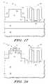
- FIG. 17Shown in FIG. 17 is semiconductor device 50 after forming a gate dielectric 84 on epitaxial layer 66 , a gate dielectric layer 85 on the side of silicon fill 82 , a gate dielectric layer 86 on silicon fins 78 and 80 and silicon layer 56 , and a polysilicon layer 88 after forming gate dielectrics 84 and 86 .
- gate dielectrics 84 and 86are preferably thermally grown oxide.
- An alternativewould be to use another type of gate dielectric such as a high k dielectric such as hafnium oxide. In such case the gate dielectric would be deposited over all of the surfaces shown in FIG. 17 before the formation of polysilicon layer 88 .
- Polysilicon layer 88could be replaced by another gate electrode material other than polysilicon or in addition to polysilicon.
- Transistor 96is a planar transistor having a portion of polysilicon layer 88 as the gate, source/drains 92 and 94 in epitaxial layer 66 , and sidewall spacer 90 around the gate.
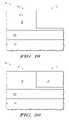
- Shown in FIG. 19is a semiconductor device 100 comprising a substrate 102 , an insulating layer 104 , a silicon layer 106 that has been patterned, and a capping layer 108 .
- Silicon layer 106has a region 110 for planar transistors and a region 112 for forming finFETs.
- Silicon layer 106has a height in region 110 that is about the same as the desired fin height and a height that is sufficient to function as a seed for SiGe epitaxial growth in region 112 . This reduced height for silicon layer 106 in region 112 is achieved by a timed etch.
- FIG. 20Shown in FIG. 20 is semiconductor device 100 after epitaxially growing a SiGe layer 114 over silicon layer 106 in region 112 while capping layer 108 is present and then removing capping layer 108 . This achieves the structure of FIG. 10 . The process continues as described for FIGS. 11-18 . This shows there are multiple techniques available to achieve the structure of FIG. 10 .
Landscapes
- Insulated Gate Type Field-Effect Transistor (AREA)
- Thin Film Transistor (AREA)
Abstract
Description
- This application is related to U.S. patent application docket number MT10667TP, titled “Semiconductor Fin Integration Using a Sacrificial Fin,” filed on even date herewith, filed by the inventors hereof, and assigned to the assignee hereof,
- 1. Field
- This disclosure relates generally to forming semiconductor fins for use in making semiconductor devices, and more specifically, to forming the semiconductor fins using a sacrificial fin.
- 2. Related Art
- The use of semiconductor fins in making semiconductor devices provides advantages over planar semiconductor devices. Transistors having a fin for the channel can be made to have lower leakage and higher drive because the gate, being on two sides of the channel, has more control of the channel. One of the desires generally relevant to semiconductor devices, including those using semiconductor fins, is to increase the density; to increase the number of devices in a given area. In the case of semiconductor fins, the minimum fins spacing is lithographically limited. Transistors using fins, however, are not expected to fit all of the requirements of an integrated circuit design. Thus, one issue is integrating the fins with planar transistors while improving density.
- Thus, there is a need to improve the density of semiconductor devices using fins while also having desirable electrical characteristics, and a further desire is to efficiently integrate semiconductor fins with planar transistors.
- The present invention is illustrated by way of example and is not limited by the accompanying figures, in which like references indicate similar elements. Elements in the figures are illustrated for simplicity and clarity and have not necessarily been drawn to scale.
FIG. 1 is a cross section of a semiconductor device at a stage in processing according to an embodiment of the invention;FIG. 2 is a cross section of the semiconductor device ofFIG. 1 at a subsequent stage in processing;FIG. 3 is a cross section of the semiconductor device ofFIG. 2 at a subsequent stage in processing;FIG. 4 is a cross section of the semiconductor device ofFIG. 3 at a subsequent stage in processing;FIG. 5 is a cross section of the semiconductor device ofFIG. 4 at a subsequent stage in processing;FIG. 6 is a cross section of the semiconductor device ofFIG. 5 at a subsequent stage in processing;FIG. 7 is a cross section of a semiconductor device at a stage in processing according to another embodiment of the invention;FIG. 8 is a cross section of the semiconductor device ofFIG. 7 at a subsequent stage in processing;FIG. 9 is a cross section of the semiconductor device ofFIG. 8 at a subsequent stage in processing;FIG. 10 is a cross section of the semiconductor device ofFIG. 9 at a subsequent stage in processing;FIG. 11 is a cross section of the semiconductor device ofFIG. 10 at a subsequent stage in processing;FIG. 12 is a cross section of the semiconductor device ofFIG. 11 at a subsequent stage in processing;FIG. 13 is a cross section of the semiconductor device ofFIG. 12 at a subsequent stage in processing;FIG. 14 is a cross section of the semiconductor device ofFIG. 13 at a subsequent stage in processing;FIG. 15 is a cross section of the semiconductor device ofFIG. 14 at a subsequent stage in processing;FIG. 16 is a cross section of the semiconductor device ofFIG. 15 at a subsequent stage in processing;FIG. 17 is a cross section of the semiconductor device ofFIG. 16 at a subsequent stage in processing;FIG. 18 is a cross section of the semiconductor device ofFIG. 17 at a subsequent stage in processing;FIG. 19 is a cross section of a semiconductor device at stage in processing for an alternative to a obtaining a semiconductor device similar to that ofFIG. 10 ; andFIG. 20 is a cross section of the semiconductor device ofFIG. 19 at a subsequent stage in processing.- In one aspect, a sacrificial fin is formed of silicon germanium (SiGe) with an overlying nitride layer. The SiGe fin is trimmed to result in the silicon nitride (nitride) layer having an overhang extending past the sides of the SiGe fin. Epitaxial silicon is grown on the sides of the SiGe fin. During the growth, the nitride overhang functions to contain the silicon growth which has the affect of reducing or eliminating the occurrence of facets in the silicon growth. The reduction or elimination of facets provides for more control of the silicon width. The SiGe fin is removed leaving two silicon fins that are then used in transistor formation. This is better understood by reference to the drawings in the following description.
- Shown in
FIG. 1 issemiconductor device 10 comprising asubstrate 12, aninsulating layer 14, a silicon germanium (SiGe)fin 16 overinsulating layer 14, and acapping layer 18 overSiGe fin 16.Substrate 12 andinsulating layer 14 and SiGefin 16 may be formed from a semiconductor-on-insulator (SOI) substrate in which the overlying semiconductor layer is SiGe.Substrate 12 can be considered a handle wafer portion because it provides structural support. In this case SiGefin 16 may be about 100 nanometers (nm) in height. Cappinglayer 18 and SiGefin 16 arise from forming a SiGe layer overinsulating layer 14 and another layer, preferably nitride in this example, over the SiGe layer. The nitride layer is patterned and the SiGe is then patterned as well. The width of SiGefin 16 is preferably the smallest that can be achieved by the lithography that is available but could be another width. SiGefin 16 is the length that is desired for the fin transistor to be formed in silicon using SiGefin 16. At the end of this length, not shown but conventional for fins, is a source/drain region that is also elevated at the same height asSiGe fin 16. This source/drain is also covered with the nitride. - Shown in
FIG. 2 issemiconductor device 10 after trimmingSiGe fin 16 which results in anoverhang 20 wherenitride layer 18 extends past the sides of trimmed SiGefin 16. Preferably the overhang is about a fourth of the width of SiGefin 16 ofFIG. 1 . Thus for an overhang on both sides ofSiGe fin 16, trimming reduces the width in half to achieve the 25% overhang ofoverhang 20. Trimming is a well known process for silicon gates. Trimming processes, such as those used for trimming polysilicon gates, may be used with the corresponding adjustment in chemistry to account for the trimming being of SiGe instead of silicon. One such method is to oxidize along the sides and remove the resulting oxide. Another is to apply an isotropic etch. - Shown in
FIG. 3 issemiconductor device 10 after epitaxially growing asilicon fin 22 on one sidewall of SiGefin 16 and asilicon fin 24 on the other side of SiGefin 16.Silicon fins overhang 20. Thus,silicon fins SiGe fin 16. Thus about 20% of the width ofSiGe fin 16 is achievable. The result is that for every sacrificial SiGe fin, there are two silicon fins. The width ofsacrificial SiGe fin 16 is of a width to achieve the desired width and spacing ofsilicon fins - Shown in
FIG. 4 issemiconductor device 10 after removingcapping layer 18 shown inFIG. 3 . The portions of cappinglayer 18 over the SiGe source/drain regions, which are not shown in the FIGs. are not removed at this step. This has the affect of exposingSiGe fin 16. - Shown in
FIG. 5 issemiconductor device 10 after removingSiGe fin 16. This leavessilicon fins layer 18 over the SiGe source/drain regions may be removed after removingSiGe fin 16. - Shown in
FIG. 6 issemiconductor device 10 after forming agate dielectric 26 onsilicon fin 22, agate dielectric 28 onsemiconductor fin 24, and apolysilicon layer 30 onsilicon fins Gate dielectric 26 and gate dielectric28 in this example are thermal oxides which may be grown in a typical fashion for gate dielectrics. An alternative would be to provide a high k gate dielectric such as hafnium oxide. In such case the gate dielectric would be deposited and would then be on the surface of insulatinglayer 14.Polysilicon layer 30 would be patterned and used as a gate. The view inFIG. 6 is unchanged by patterningpolysilicon layer 30. - Thus it is seen that fins can be made using a sacrificial SiGe fin to grow sublithographic silicon fins. With the trimming of the SiGe fin, there is left an overhang of an overlying capping layer. The overhang of the overlying capping layer constrains the epitaxial silicon growth to occur in one direction only so that facets do not occur or at least are significantly reduced. Thus
fins - Shown in
FIG. 7 is asemiconductor device 50 comprising a substrate52 (handle wafer portion), an insulatinglayer 54 oversubstrate 52, and asilicon layer 56 over the insulating layer. This is similar to a conventional SOI wafer except thatsilicon layer 56 is preferably thinner than the semiconductor layer on a conventional SOI wafer. For example,silicon layer 56 is preferably about 20 nm or even less. This can be achieved in a conventional SOI substrate by oxidizing the semiconductor surface of a conventional SOI substrate and then removing the oxide. The thickness can be quite thin because its purpose is as a seed layer. It may be thicker than the minimum but because it will be part of the channel, it should still be sufficiently thin to allow sufficient channel control, especially to avoid excessive off-state leakage. - Shown in
FIG. 8 issemiconductor device 50 after growing aSiGe layer 58 onsilicon layer 56. The height ofSiGe layer 58 is the desired height of the fins that will be subsequently formed, which is about100 nm but could be another height. This structure ofsemiconductor device 50 shown inFIG. 8 may also be directly available commercially from a vendor who may make it by this or another process such as layer transfer. - Shown in
FIG. 9 issemiconductor device 50 after forming acapping layer 60, preferably of oxide, overSiGe layer 58 and then removing a portion ofSiGe layer 58 andcapping layer 60. The removed portion is from aregion 62 for forming planar transistors and the remaining portion ofSiGe layer 58 is in aregion 64 for forming fin transistors (finFETs).Silicon layer 56 is exposed inregion 62. - Shown in
FIG. 10 issemiconductor device 50 after selectively growing epitaxial silicon onsilicon layer 56 to form anepitaxial layer 66 that will function as the body for planar transistors and then removingcapping layer 60.Dotted line 68 shows the previous surface ofsilicon layer 56.Line 68 is dotted because the demarcation ofsilicon layer 56 would unlikely to be discernible after performing the epitaxial growth to formepitaxial layer 66. - Shown in
FIG. 11 issemiconductor device 50 after formingisolation regions epitaxial layer 66 and forming acapping layer 74, preferably of nitride, overepitaxial layer 66,isolation regions SiGe layer 58. Cappinglayer 74 is preferably about 20-50 nm in thickness. - Shown in
FIG. 12 issemiconductor device 50 after performing a patterned etch through cappinglayer 74,SiGe layer 58, andsilicon layer 56. This leaves a fin of SiGe similar to that ofFIG. 1 and the dimensions may be the same. A difference is thatSiGe layer 58 is over a silicon layer,silicon layer 56, whereasSiGe fin 16 is directly on an insulating layer. In this cross section ofFIG. 12 , only the fin portion ofSiGe layer 58 is shown, but source/drain portions at the ends of the fin are present and covered bynitride layer 74. - Shown in
FIG. 13 issemiconductor device 50 after trimmingSiGe layer 58 andsilicon layer 56. The trimming is the same as for the trimming shown inFIG. 2 except that both SiGe and silicon are being trimmed so if an isotropic etch is used, it preferably is not selective, or at least not significantly so, between silicon and SiGe. Cappinglayer 74 thus overhangs past the sides of trimmed SiGe layer andsilicon layer 56 by anoverhang 76. The trimming is symmetrical so cappinglayer 74 overhangs on both sides. The trim also etches the side ofepitaxial layer 66. - Shown in
FIG. 14 issemiconductor device 50 aftersilicon fins SiGe layer 58 andsilicon layer 56, and silicon fill82 is simultaneously grown on the side ofepitaxial layer 66. Thesesilicon fins silicon fins FIG. 3 except for the growth fromsilicon layer 56. Thus,silicon fins SiGe layer 58 ofFIG. 12 . As described relative toFIG. 3 , the result is that for every sacrificial SiGe fin, there are two silicon fins. The width of58 sacrificial SiGe layer is of a width to achieve the desired width and spacing forsilicon fins silicon layer 56 andsilicon fins silicon fins - Shown in
FIG. 15 issemiconductor device 50 after removingcapping layer 74 over the fin portion ofSiGe layer 58, which is inregion 64. The portions of cappinglayer 74 overregion 62 and over the source/drain regions (not shown) are not removed at this time. - Shown in
FIG. 16 issemiconductor device 50 after removing the fin portion ofSiGe layer 58. The source/drain regions are not removed because they are still capped by cappinglayer 74. The resulting structure hasfins silicon layer 56 between them. The removing of SiGe is selective to silicon. An etch chemistry that is effective for this purpose is thermal gaseous HCl. Other selective etches include plasma fluorine chemistries or peroxide wet etches. Cappinglayer 74 overregion 62 and over the source/drains is removed after the SiGe fin portion is removed. - Shown in
FIG. 17 issemiconductor device 50 after forming agate dielectric 84 onepitaxial layer 66, agate dielectric layer 85 on the side of silicon fill82, agate dielectric layer 86 onsilicon fins silicon layer 56, and apolysilicon layer 88 after forminggate dielectrics gate dielectrics FIG. 17 before the formation ofpolysilicon layer 88.Polysilicon layer 88 could be replaced by another gate electrode material other than polysilicon or in addition to polysilicon. - Shown in
FIG. 18 issemiconductor device 50 after patterningpolysilicon layer 88 and forming atransistor 96 inregion 62 and atransistor 98 inregion 64.Transistor 96 is a planar transistor having a portion ofpolysilicon layer 88 as the gate, source/drains92 and94 inepitaxial layer 66, andsidewall spacer 90 around the gate. - Thus it is seen that there is an integration on the same substrate of an integrated circuit of a planar transistor and a finFET. This shows that this integration may be achieved while using the overhang to achieve the reduced faceting while achieving sublithographic pitch by having two silicon fins per sacrificial fin with the sacrificial fins being at the minimum pitch. Also the height of the planar transistor above insulating
layer 54 is substantially the same as the height of the finFET. This is beneficial for subsequent processing. - Shown in
FIG. 19 is asemiconductor device 100 comprising asubstrate 102, an insulatinglayer 104, asilicon layer 106 that has been patterned, and acapping layer 108.Silicon layer 106 has aregion 110 for planar transistors and aregion 112 for forming finFETs.Silicon layer 106 has a height inregion 110 that is about the same as the desired fin height and a height that is sufficient to function as a seed for SiGe epitaxial growth inregion 112. This reduced height forsilicon layer 106 inregion 112 is achieved by a timed etch. - Shown in
FIG. 20 issemiconductor device 100 after epitaxially growing aSiGe layer 114 oversilicon layer 106 inregion 112 while cappinglayer 108 is present and then removingcapping layer 108. This achieves the structure ofFIG. 10 . The process continues as described forFIGS. 11-18 . This shows there are multiple techniques available to achieve the structure ofFIG. 10 . - Although the invention is described herein with reference to specific embodiments, various modifications and changes can be made without departing from the scope of the present invention as set forth in the claims below. For example, different materials may be used than those described. For example, the sacrificial fin may be a different material than SiGe and the fins to be left remaining may be a different material than silicon. Accordingly, the specification and figures are to be regarded in an illustrative rather than a restrictive sense, and all such modifications are intended to be included within the scope of the present invention. Any benefits, advantages, or solutions to problems that are described herein with regard to specific embodiments are not intended to be construed as a critical, required, or essential feature or element of any or all the claims.
- Furthermore, the terms “a” or “an,” as used herein, are defined as one or more than one. Also, the use of introductory phrases such as “at least one” and “one or more” in the claims should not be construed to imply that the introduction of another claim element by the indefinite articles “a” or “an” limits any particular claim containing such introduced claim element to inventions containing only one such element, even when the same claim includes the introductory phrases “one or more” or “at least one” and indefinite articles such as “a” or “an.” The same holds true for the use of definite articles.
- Unless stated otherwise, terms such as “first” and “second” are used to arbitrarily distinguish between the elements such terms describe. Thus, these terms are not necessarily intended to indicate temporal or other prioritization of such elements.
Claims (20)
Priority Applications (1)
| Application Number | Priority Date | Filing Date | Title |
|---|---|---|---|
| US11/678,327US7772048B2 (en) | 2007-02-23 | 2007-02-23 | Forming semiconductor fins using a sacrificial fin |
Applications Claiming Priority (1)
| Application Number | Priority Date | Filing Date | Title |
|---|---|---|---|
| US11/678,327US7772048B2 (en) | 2007-02-23 | 2007-02-23 | Forming semiconductor fins using a sacrificial fin |
Publications (2)
| Publication Number | Publication Date |
|---|---|
| US20080206934A1true US20080206934A1 (en) | 2008-08-28 |
| US7772048B2 US7772048B2 (en) | 2010-08-10 |
Family
ID=39716363
Family Applications (1)
| Application Number | Title | Priority Date | Filing Date |
|---|---|---|---|
| US11/678,327Active2028-02-14US7772048B2 (en) | 2007-02-23 | 2007-02-23 | Forming semiconductor fins using a sacrificial fin |
Country Status (1)
| Country | Link |
|---|---|
| US (1) | US7772048B2 (en) |
Cited By (12)
| Publication number | Priority date | Publication date | Assignee | Title |
|---|---|---|---|---|
| US20110129978A1 (en)* | 2009-12-01 | 2011-06-02 | Kangguo Cheng | Method and structure for forming finfets with multiple doping regions on a same chip |
| US20130037869A1 (en)* | 2011-08-10 | 2013-02-14 | Kabushiki Kaisha Toshiba | Semiconductor device and manufacturing method of semiconductor device |
| US20130059401A1 (en)* | 2011-09-01 | 2013-03-07 | Gaku Sudo | Method for manufacturing semiconductor device |
| US20130228863A1 (en)* | 2012-03-02 | 2013-09-05 | Semiconductor Manufacturing International Corp. | Fin field effect transistor and fabrication method |
| US20130320423A1 (en)* | 2012-05-31 | 2013-12-05 | International Business Machines Corporation | Wrap-around fin for contacting a capacitor strap of a dram |
| WO2015026590A1 (en)* | 2013-08-19 | 2015-02-26 | Applied Materials, Inc. | Fin formation by epitaxial deposition |
| US20150318355A1 (en)* | 2014-05-02 | 2015-11-05 | Samsung Electronics Co., Ltd. | Methods of forming defect-free srb onto lattice-mismatched substrates and defect-free fins on insulators |
| US9281303B2 (en) | 2014-05-28 | 2016-03-08 | International Business Machines Corporation | Electrostatic discharge devices and methods of manufacture |
| US9397215B1 (en)* | 2015-09-04 | 2016-07-19 | International Business Machines Corporation | FinFET with reduced source and drain resistance |
| US9437699B2 (en) | 2014-10-03 | 2016-09-06 | Taiwan Semiconductor Manufacturing Company Limited | Method of forming nanowires |
| US10347657B1 (en)* | 2018-01-11 | 2019-07-09 | International Business Machines Corporation | Semiconductor circuit including nanosheets and fins on the same wafer |
| US12009228B2 (en) | 2015-02-03 | 2024-06-11 | Applied Materials, Inc. | Low temperature chuck for plasma processing systems |
Families Citing this family (11)
| Publication number | Priority date | Publication date | Assignee | Title |
|---|---|---|---|---|
| US7960791B2 (en)* | 2005-06-24 | 2011-06-14 | International Business Machines Corporation | Dense pitch bulk FinFET process by selective EPI and etch |
| JP2007299951A (en)* | 2006-04-28 | 2007-11-15 | Toshiba Corp | Semiconductor device and manufacturing method thereof |
| JP2009206306A (en)* | 2008-02-28 | 2009-09-10 | Seiko Epson Corp | Method for manufacturing semiconductor apparatus, and method of manufacturing electro-optical apparatus |
| US8946027B2 (en) | 2012-02-07 | 2015-02-03 | International Business Machines Corporation | Replacement-gate FinFET structure and process |
| US8617961B1 (en) | 2012-07-18 | 2013-12-31 | International Business Machines Corporation | Post-gate isolation area formation for fin field effect transistor device |
| US8916932B2 (en) | 2013-05-08 | 2014-12-23 | International Business Machines Corporation | Semiconductor device including FINFET structures with varied epitaxial regions, related method and design structure |
| US9412603B2 (en) | 2013-11-19 | 2016-08-09 | Applied Materials, Inc. | Trimming silicon fin width through oxidation and etch |
| US9484201B2 (en) | 2015-02-23 | 2016-11-01 | International Business Machines Corporation | Epitaxial silicon germanium fin formation using sacrificial silicon fin templates |
| US9543435B1 (en)* | 2015-10-20 | 2017-01-10 | International Business Machines Corporation | Asymmetric multi-gate finFET |
| US10204781B1 (en) | 2018-02-14 | 2019-02-12 | Applied Materials, Inc. | Methods for bottom up fin structure formation |
| US10439047B2 (en) | 2018-02-14 | 2019-10-08 | Applied Materials, Inc. | Methods for etch mask and fin structure formation |
Citations (88)
| Publication number | Priority date | Publication date | Assignee | Title |
|---|---|---|---|---|
| US5023203A (en)* | 1988-07-28 | 1991-06-11 | Korea Electronics & Telecommunications Research Institute Et Al. | Method of patterning fine line width semiconductor topology using a spacer |
| US5399507A (en)* | 1994-06-27 | 1995-03-21 | Motorola, Inc. | Fabrication of mixed thin-film and bulk semiconductor substrate for integrated circuit applications |
| US5563077A (en)* | 1992-04-24 | 1996-10-08 | Hyundai Electronics Industries Co., Ltd. | Method of fabricating a thin film transistor having vertical channel |
| US5675164A (en)* | 1995-06-07 | 1997-10-07 | International Business Machines Corporation | High performance multi-mesa field effect transistor |
| US5705414A (en)* | 1995-12-21 | 1998-01-06 | Siemens Aktiengesellschaft | Method for producing a gate electrode for an MOS structure |
| US5740099A (en)* | 1995-02-07 | 1998-04-14 | Nec Corporation | Semiconductor memory device having peripheral circuit and interface circuit fabricated on bulk region out of silicon-on-insulator region for memory cells |
| US5942787A (en)* | 1996-11-18 | 1999-08-24 | Advanced Micro Devices, Inc. | Small gate electrode MOSFET |
| US6107125A (en)* | 1997-06-18 | 2000-08-22 | International Business Machines Corporation | SOI/bulk hybrid substrate and method of forming the same |
| US6171910B1 (en)* | 1999-07-21 | 2001-01-09 | Motorola Inc. | Method for forming a semiconductor device |
| US6222259B1 (en)* | 1998-09-15 | 2001-04-24 | Hyundai Electronics Industries Co., Ltd. | Stack package and method of fabricating the same |
| US6225201B1 (en)* | 1998-03-09 | 2001-05-01 | Advanced Micro Devices, Inc. | Ultra short transistor channel length dictated by the width of a sidewall spacer |
| US20010009784A1 (en)* | 1998-01-09 | 2001-07-26 | Yanjun Ma | Structure and method of making a sub-micron MOS transistor |
| US6271113B1 (en)* | 1999-04-15 | 2001-08-07 | Hyundai Electronics Industries Co., Ltd. | Method for forming wiring in semiconductor device |
| US6337516B1 (en)* | 1998-07-16 | 2002-01-08 | International Business Machines Corporation | Technique for extending the limits of photolithography |
| US6358827B1 (en)* | 2001-01-19 | 2002-03-19 | Taiwan Semiconductor Manufacturing Company | Method of forming a squared-off, vertically oriented polysilicon spacer gate |
| US6362057B1 (en)* | 1999-10-26 | 2002-03-26 | Motorola, Inc. | Method for forming a semiconductor device |
| US6372559B1 (en)* | 2000-11-09 | 2002-04-16 | International Business Machines Corporation | Method for self-aligned vertical double-gate MOSFET |
| US6391753B1 (en)* | 2000-06-20 | 2002-05-21 | Advanced Micro Devices, Inc. | Process for forming gate conductors |
| US20020130354A1 (en)* | 2001-03-13 | 2002-09-19 | National Inst. Of Advanced Ind. Science And Tech. | Double-gate field-effect transistor, integrated circuit using the transistor and method of manufacturing the same |
| US6458662B1 (en)* | 2001-04-04 | 2002-10-01 | Advanced Micro Devices, Inc. | Method of fabricating a semiconductor device having an asymmetrical dual-gate silicon-germanium (SiGe) channel MOSFET and a device thereby formed |
| US20020140039A1 (en)* | 2000-11-13 | 2002-10-03 | International Business Machines Corporation | Double gate trench transistor |
| US6475869B1 (en)* | 2001-02-26 | 2002-11-05 | Advanced Micro Devices, Inc. | Method of forming a double gate transistor having an epitaxial silicon/germanium channel region |
| US20030027059A1 (en)* | 2001-07-31 | 2003-02-06 | Giorgio Schweeger | Method for producing a mask and method for fabricating a semiconductor device |
| US6524901B1 (en)* | 2002-06-20 | 2003-02-25 | Micron Technology, Inc. | Method for forming a notched damascene planar poly/metal gate |
| US20030067017A1 (en)* | 2001-10-05 | 2003-04-10 | Meikei Ieong | Variable threshold voltage double gated transistors and method of fabrication |
| US6548345B2 (en)* | 1999-06-16 | 2003-04-15 | International Business Machines Corporation | Method of fabricating trench for SOI merged logic DRAM |
| US20030102497A1 (en)* | 2001-12-04 | 2003-06-05 | International Business Machines Corporation | Multiple-plane finFET CMOS |
| US6583469B1 (en)* | 2002-01-28 | 2003-06-24 | International Business Machines Corporation | Self-aligned dog-bone structure for FinFET applications and methods to fabricate the same |
| US6596642B2 (en)* | 1997-03-14 | 2003-07-22 | Micron Technology, Inc. | Material removal method for forming a structure |
| US20030146488A1 (en)* | 2001-12-28 | 2003-08-07 | Hajime Nagano | Manufacturing method of partial SOI wafer, semiconductor device using the partial SOI wafer and manufacturing method thereof |
| US20030151077A1 (en)* | 2002-02-13 | 2003-08-14 | Leo Mathew | Method of forming a vertical double gate semiconductor device and structure thereof |
| US20030178677A1 (en)* | 2002-03-19 | 2003-09-25 | International Business Machines Corporation | Strained fin fets structure and method |
| US20030193058A1 (en)* | 2002-04-12 | 2003-10-16 | International Business Machines Corporation | Integrated circuit with capacitors having fin structure |
| US6642090B1 (en)* | 2002-06-03 | 2003-11-04 | International Business Machines Corporation | Fin FET devices from bulk semiconductor and method for forming |
| US6645797B1 (en)* | 2002-12-06 | 2003-11-11 | Advanced Micro Devices, Inc. | Method for forming fins in a FinFET device using sacrificial carbon layer |
| US20040038436A1 (en)* | 2002-08-09 | 2004-02-26 | Hitachi, Ltd. | Method of manufacturing a semiconductor integrated circuit device |
| US6709982B1 (en)* | 2002-11-26 | 2004-03-23 | Advanced Micro Devices, Inc. | Double spacer FinFET formation |
| US20040119100A1 (en)* | 2002-12-19 | 2004-06-24 | International Business Machines Corporation | Dense dual-plane devices |
| US6762101B2 (en)* | 2002-04-10 | 2004-07-13 | International Business Machines Corporation | Damascene double-gate FET |
| US20040150044A1 (en)* | 2003-01-21 | 2004-08-05 | Hajime Nagano | Element formation substrate, method of manufacturing the same, and semiconductor device |
| US20040161898A1 (en)* | 2002-04-11 | 2004-08-19 | Fried David M. | Dual double gate transistor and method for forming |
| US6800885B1 (en)* | 2003-03-12 | 2004-10-05 | Advance Micro Devices, Inc. | Asymmetrical double gate or all-around gate MOSFET devices and methods for making same |
| US6800905B2 (en)* | 2001-12-14 | 2004-10-05 | International Business Machines Corporation | Implanted asymmetric doped polysilicon gate FinFET |
| US6812119B1 (en)* | 2003-07-08 | 2004-11-02 | Advanced Micro Devices, Inc. | Narrow fins by oxidation in double-gate finfet |
| US20040219722A1 (en)* | 2003-05-01 | 2004-11-04 | Pham Daniel T. | Method for forming a double-gated semiconductor device |
| US20050048727A1 (en)* | 2003-09-03 | 2005-03-03 | Advanced Micro Devices, Inc. | Formation of finfet using a sidewall epitaxial layer |
| US20050059236A1 (en)* | 2003-09-11 | 2005-03-17 | Akio Nishida | Semiconductor device and a method of manufacturing the same |
| US6872647B1 (en)* | 2003-05-06 | 2005-03-29 | Advanced Micro Devices, Inc. | Method for forming multiple fins in a semiconductor device |
| US20050077553A1 (en)* | 2003-10-14 | 2005-04-14 | Kim Sung-Min | Methods of forming multi fin FETs using sacrificial fins and devices so formed |
| US20050104091A1 (en)* | 2003-11-04 | 2005-05-19 | Tabery Cyrus E. | Self aligned damascene gate |
| US20050110085A1 (en)* | 2003-11-20 | 2005-05-26 | Huilong Zhu | Dual gate finfet |
| US20050145954A1 (en)* | 2004-01-05 | 2005-07-07 | International Business Machines Corporation | Structures and methods for making strained mosfets |
| US6921963B2 (en)* | 2003-01-23 | 2005-07-26 | Advanced Micro Devices, Inc | Narrow fin FinFET |
| US6949420B1 (en)* | 2004-03-12 | 2005-09-27 | Sony Corporation | Silicon-on-insulator (SOI) substrate having dual surface crystallographic orientations and method of forming same |
| US6951783B2 (en)* | 2003-10-28 | 2005-10-04 | Freescale Semiconductor, Inc. | Confined spacers for double gate transistor semiconductor fabrication process |
| US20060008973A1 (en)* | 2004-07-07 | 2006-01-12 | Phua Timothy W H | Selective oxide trimming to improve metal T-gate transistor |
| US6987068B2 (en)* | 2003-06-14 | 2006-01-17 | Intel Corporation | Methods to planarize semiconductor device and passivation layer |
| US7015124B1 (en)* | 2003-04-28 | 2006-03-21 | Advanced Micro Devices, Inc. | Use of amorphous carbon for gate patterning |
| US20060084249A1 (en)* | 2004-10-19 | 2006-04-20 | Kabushiki Kaisha Toshiba | Method for manufacturing a hybrid semiconductor wafer having a buried oxide film |
| US20060091450A1 (en)* | 2004-11-01 | 2006-05-04 | Huilong Zhu | Dual function FinFET, finmemory and method of manufacture |
| US7045401B2 (en)* | 2003-06-23 | 2006-05-16 | Sharp Laboratories Of America, Inc. | Strained silicon finFET device |
| US20060110928A1 (en)* | 2004-10-07 | 2006-05-25 | Bart Degroote | Etching of structures with high topography |
| US7064415B1 (en)* | 2002-08-13 | 2006-06-20 | Newport Fab Llc | Self-aligned bipolar transistor having increased manufacturability |
| US7084018B1 (en)* | 2004-05-05 | 2006-08-01 | Advanced Micro Devices, Inc. | Sacrificial oxide for minimizing box undercut in damascene FinFET |
| US20060223265A1 (en)* | 2005-03-31 | 2006-10-05 | Hynix Semiconductor Inc. | Vertical transistor of semiconductor device and method for forming the same |
| US7138302B2 (en)* | 2004-01-12 | 2006-11-21 | Advanced Micro Devices, Inc. | Method of fabricating an integrated circuit channel region |
| US7141476B2 (en)* | 2004-06-18 | 2006-11-28 | Freescale Semiconductor, Inc. | Method of forming a transistor with a bottom gate |
| US7176534B2 (en)* | 2002-11-08 | 2007-02-13 | International Business Machines Corporation | Low resistance T-gate MOSFET device using a damascene gate process and an innovative oxide removal etch |
| US7183142B2 (en)* | 2005-01-13 | 2007-02-27 | International Business Machines Corporation | FinFETs with long gate length at high density |
| US7192876B2 (en)* | 2003-05-22 | 2007-03-20 | Freescale Semiconductor, Inc. | Transistor with independent gate structures |
| US20070065990A1 (en)* | 2005-09-16 | 2007-03-22 | Bart Degroote | Recursive spacer defined patterning |
| US7198995B2 (en)* | 2003-12-12 | 2007-04-03 | International Business Machines Corporation | Strained finFETs and method of manufacture |
| US20070099350A1 (en)* | 2005-10-27 | 2007-05-03 | International Business Machines Corporation | Structure and method of fabricating finfet with buried channel |
| US7262084B2 (en)* | 2004-04-15 | 2007-08-28 | International Business Machines Corporation | Methods for manufacturing a finFET using a conventional wafer and apparatus manufactured therefrom |
| US7265059B2 (en)* | 2005-09-30 | 2007-09-04 | Freescale Semiconductor, Inc. | Multiple fin formation |
| US7265417B2 (en)* | 2000-10-18 | 2007-09-04 | International Business Machines Corporation | Method of fabricating semiconductor side wall fin |
| US7288802B2 (en)* | 2005-07-27 | 2007-10-30 | International Business Machines Corporation | Virtual body-contacted trigate |
| US7323748B2 (en)* | 2003-08-28 | 2008-01-29 | Kabushiki Kaisha Toshiba | Semiconductor device having epitaxial layer |
| US7341916B2 (en)* | 2005-11-10 | 2008-03-11 | Atmel Corporation | Self-aligned nanometer-level transistor defined without lithography |
| US7348641B2 (en)* | 2004-08-31 | 2008-03-25 | International Business Machines Corporation | Structure and method of making double-gated self-aligned finFET having gates of different lengths |
| US7387937B2 (en)* | 2005-06-21 | 2008-06-17 | International Business Machines Corporation | Thermal dissipation structures for FinFETs |
| US7396711B2 (en)* | 2005-12-27 | 2008-07-08 | Intel Corporation | Method of fabricating a multi-cornered film |
| US7407890B2 (en)* | 2006-04-21 | 2008-08-05 | International Business Machines Corporation | Patterning sub-lithographic features with variable widths |
| US7432122B2 (en)* | 2006-01-06 | 2008-10-07 | Freescale Semiconductor, Inc. | Electronic device and a process for forming the electronic device |
| US7455956B2 (en)* | 2004-09-02 | 2008-11-25 | Micron Technology, Inc. | Method to align mask patterns |
| US7473967B2 (en)* | 2003-05-30 | 2009-01-06 | Panasonic Corporation | Strained channel finFET device |
| US7491589B2 (en)* | 2004-06-11 | 2009-02-17 | International Business Machines Corporation | Back gate FinFET SRAM |
| US7498225B1 (en)* | 2003-12-04 | 2009-03-03 | Advanced Micro Devices, Inc. | Systems and methods for forming multiple fin structures using metal-induced-crystallization |
Family Cites Families (10)
| Publication number | Priority date | Publication date | Assignee | Title |
|---|---|---|---|---|
| JP2526786B2 (en)* | 1993-05-22 | 1996-08-21 | 日本電気株式会社 | Semiconductor device and manufacturing method thereof |
| US6329124B1 (en)* | 1999-05-26 | 2001-12-11 | Advanced Micro Devices | Method to produce high density memory cells and small spaces by using nitride spacer |
| JP4322453B2 (en)* | 2001-09-27 | 2009-09-02 | 株式会社東芝 | Semiconductor device and manufacturing method thereof |
| US6664173B2 (en)* | 2002-01-09 | 2003-12-16 | Intel Corporation | Hardmask gate patterning technique for all transistors using spacer gate approach for critical dimension control |
| JP3782021B2 (en)* | 2002-02-22 | 2006-06-07 | 株式会社東芝 | Semiconductor device, semiconductor device manufacturing method, and semiconductor substrate manufacturing method |
| US6657252B2 (en)* | 2002-03-19 | 2003-12-02 | International Business Machines Corporation | FinFET CMOS with NVRAM capability |
| US6911383B2 (en)* | 2003-06-26 | 2005-06-28 | International Business Machines Corporation | Hybrid planar and finFET CMOS devices |
| US7456476B2 (en)* | 2003-06-27 | 2008-11-25 | Intel Corporation | Nonplanar semiconductor device with partially or fully wrapped around gate electrode and methods of fabrication |
| US7514367B2 (en)* | 2005-06-17 | 2009-04-07 | Macronix International Co., Ltd. | Method for manufacturing a narrow structure on an integrated circuit |
| US7611955B2 (en)* | 2006-06-15 | 2009-11-03 | Freescale Semiconductor, Inc. | Method of forming a bipolar transistor and semiconductor component thereof |
- 2007
- 2007-02-23USUS11/678,327patent/US7772048B2/enactiveActive
Patent Citations (99)
| Publication number | Priority date | Publication date | Assignee | Title |
|---|---|---|---|---|
| US5023203A (en)* | 1988-07-28 | 1991-06-11 | Korea Electronics & Telecommunications Research Institute Et Al. | Method of patterning fine line width semiconductor topology using a spacer |
| US5563077A (en)* | 1992-04-24 | 1996-10-08 | Hyundai Electronics Industries Co., Ltd. | Method of fabricating a thin film transistor having vertical channel |
| US5399507A (en)* | 1994-06-27 | 1995-03-21 | Motorola, Inc. | Fabrication of mixed thin-film and bulk semiconductor substrate for integrated circuit applications |
| US5740099A (en)* | 1995-02-07 | 1998-04-14 | Nec Corporation | Semiconductor memory device having peripheral circuit and interface circuit fabricated on bulk region out of silicon-on-insulator region for memory cells |
| US5675164A (en)* | 1995-06-07 | 1997-10-07 | International Business Machines Corporation | High performance multi-mesa field effect transistor |
| US5705414A (en)* | 1995-12-21 | 1998-01-06 | Siemens Aktiengesellschaft | Method for producing a gate electrode for an MOS structure |
| US5942787A (en)* | 1996-11-18 | 1999-08-24 | Advanced Micro Devices, Inc. | Small gate electrode MOSFET |
| US6596642B2 (en)* | 1997-03-14 | 2003-07-22 | Micron Technology, Inc. | Material removal method for forming a structure |
| US6107125A (en)* | 1997-06-18 | 2000-08-22 | International Business Machines Corporation | SOI/bulk hybrid substrate and method of forming the same |
| US20010009784A1 (en)* | 1998-01-09 | 2001-07-26 | Yanjun Ma | Structure and method of making a sub-micron MOS transistor |
| US6225201B1 (en)* | 1998-03-09 | 2001-05-01 | Advanced Micro Devices, Inc. | Ultra short transistor channel length dictated by the width of a sidewall spacer |
| US6337516B1 (en)* | 1998-07-16 | 2002-01-08 | International Business Machines Corporation | Technique for extending the limits of photolithography |
| US6222259B1 (en)* | 1998-09-15 | 2001-04-24 | Hyundai Electronics Industries Co., Ltd. | Stack package and method of fabricating the same |
| US6271113B1 (en)* | 1999-04-15 | 2001-08-07 | Hyundai Electronics Industries Co., Ltd. | Method for forming wiring in semiconductor device |
| US6548345B2 (en)* | 1999-06-16 | 2003-04-15 | International Business Machines Corporation | Method of fabricating trench for SOI merged logic DRAM |
| US6171910B1 (en)* | 1999-07-21 | 2001-01-09 | Motorola Inc. | Method for forming a semiconductor device |
| US6362057B1 (en)* | 1999-10-26 | 2002-03-26 | Motorola, Inc. | Method for forming a semiconductor device |
| US6391753B1 (en)* | 2000-06-20 | 2002-05-21 | Advanced Micro Devices, Inc. | Process for forming gate conductors |
| US7265417B2 (en)* | 2000-10-18 | 2007-09-04 | International Business Machines Corporation | Method of fabricating semiconductor side wall fin |
| US6372559B1 (en)* | 2000-11-09 | 2002-04-16 | International Business Machines Corporation | Method for self-aligned vertical double-gate MOSFET |
| US6472258B1 (en)* | 2000-11-13 | 2002-10-29 | International Business Machines Corporation | Double gate trench transistor |
| US20020140039A1 (en)* | 2000-11-13 | 2002-10-03 | International Business Machines Corporation | Double gate trench transistor |
| US6358827B1 (en)* | 2001-01-19 | 2002-03-19 | Taiwan Semiconductor Manufacturing Company | Method of forming a squared-off, vertically oriented polysilicon spacer gate |
| US6475869B1 (en)* | 2001-02-26 | 2002-11-05 | Advanced Micro Devices, Inc. | Method of forming a double gate transistor having an epitaxial silicon/germanium channel region |
| US20020130354A1 (en)* | 2001-03-13 | 2002-09-19 | National Inst. Of Advanced Ind. Science And Tech. | Double-gate field-effect transistor, integrated circuit using the transistor and method of manufacturing the same |
| US6458662B1 (en)* | 2001-04-04 | 2002-10-01 | Advanced Micro Devices, Inc. | Method of fabricating a semiconductor device having an asymmetrical dual-gate silicon-germanium (SiGe) channel MOSFET and a device thereby formed |
| US20030027059A1 (en)* | 2001-07-31 | 2003-02-06 | Giorgio Schweeger | Method for producing a mask and method for fabricating a semiconductor device |
| US20030067017A1 (en)* | 2001-10-05 | 2003-04-10 | Meikei Ieong | Variable threshold voltage double gated transistors and method of fabrication |
| US20030102497A1 (en)* | 2001-12-04 | 2003-06-05 | International Business Machines Corporation | Multiple-plane finFET CMOS |
| US6800905B2 (en)* | 2001-12-14 | 2004-10-05 | International Business Machines Corporation | Implanted asymmetric doped polysilicon gate FinFET |
| US20030146488A1 (en)* | 2001-12-28 | 2003-08-07 | Hajime Nagano | Manufacturing method of partial SOI wafer, semiconductor device using the partial SOI wafer and manufacturing method thereof |
| US20040007738A1 (en)* | 2002-01-28 | 2004-01-15 | International Business Machines Corporation | Self-aligned dog-bone structure for FinFET applications and methods to fabricate the same |
| US6583469B1 (en)* | 2002-01-28 | 2003-06-24 | International Business Machines Corporation | Self-aligned dog-bone structure for FinFET applications and methods to fabricate the same |
| US20030151077A1 (en)* | 2002-02-13 | 2003-08-14 | Leo Mathew | Method of forming a vertical double gate semiconductor device and structure thereof |
| US20030178677A1 (en)* | 2002-03-19 | 2003-09-25 | International Business Machines Corporation | Strained fin fets structure and method |
| US20030201458A1 (en)* | 2002-03-19 | 2003-10-30 | Clark William F. | Strained fin fets structure and method |
| US6767793B2 (en)* | 2002-03-19 | 2004-07-27 | International Business Machines Corporation | Strained fin FETs structure and method |
| US6762101B2 (en)* | 2002-04-10 | 2004-07-13 | International Business Machines Corporation | Damascene double-gate FET |
| US20040161898A1 (en)* | 2002-04-11 | 2004-08-19 | Fried David M. | Dual double gate transistor and method for forming |
| US7101741B2 (en)* | 2002-04-11 | 2006-09-05 | International Business Machines Corporation | Dual double gate transistor and method for forming |
| US20030193058A1 (en)* | 2002-04-12 | 2003-10-16 | International Business Machines Corporation | Integrated circuit with capacitors having fin structure |
| US6642090B1 (en)* | 2002-06-03 | 2003-11-04 | International Business Machines Corporation | Fin FET devices from bulk semiconductor and method for forming |
| US6524901B1 (en)* | 2002-06-20 | 2003-02-25 | Micron Technology, Inc. | Method for forming a notched damascene planar poly/metal gate |
| US20040038436A1 (en)* | 2002-08-09 | 2004-02-26 | Hitachi, Ltd. | Method of manufacturing a semiconductor integrated circuit device |
| US7064415B1 (en)* | 2002-08-13 | 2006-06-20 | Newport Fab Llc | Self-aligned bipolar transistor having increased manufacturability |
| US7291536B1 (en)* | 2002-08-13 | 2007-11-06 | Newport Fab, Llc | Fabricating a self-aligned bipolar transistor having increased manufacturability |
| US7176534B2 (en)* | 2002-11-08 | 2007-02-13 | International Business Machines Corporation | Low resistance T-gate MOSFET device using a damascene gate process and an innovative oxide removal etch |
| US6709982B1 (en)* | 2002-11-26 | 2004-03-23 | Advanced Micro Devices, Inc. | Double spacer FinFET formation |
| US6645797B1 (en)* | 2002-12-06 | 2003-11-11 | Advanced Micro Devices, Inc. | Method for forming fins in a FinFET device using sacrificial carbon layer |
| US20040119100A1 (en)* | 2002-12-19 | 2004-06-24 | International Business Machines Corporation | Dense dual-plane devices |
| US20040150044A1 (en)* | 2003-01-21 | 2004-08-05 | Hajime Nagano | Element formation substrate, method of manufacturing the same, and semiconductor device |
| US6921963B2 (en)* | 2003-01-23 | 2005-07-26 | Advanced Micro Devices, Inc | Narrow fin FinFET |
| US6800885B1 (en)* | 2003-03-12 | 2004-10-05 | Advance Micro Devices, Inc. | Asymmetrical double gate or all-around gate MOSFET devices and methods for making same |
| US7015124B1 (en)* | 2003-04-28 | 2006-03-21 | Advanced Micro Devices, Inc. | Use of amorphous carbon for gate patterning |
| US20040219722A1 (en)* | 2003-05-01 | 2004-11-04 | Pham Daniel T. | Method for forming a double-gated semiconductor device |
| US6872647B1 (en)* | 2003-05-06 | 2005-03-29 | Advanced Micro Devices, Inc. | Method for forming multiple fins in a semiconductor device |
| US7192876B2 (en)* | 2003-05-22 | 2007-03-20 | Freescale Semiconductor, Inc. | Transistor with independent gate structures |
| US7473967B2 (en)* | 2003-05-30 | 2009-01-06 | Panasonic Corporation | Strained channel finFET device |
| US6987068B2 (en)* | 2003-06-14 | 2006-01-17 | Intel Corporation | Methods to planarize semiconductor device and passivation layer |
| US20060113522A1 (en)* | 2003-06-23 | 2006-06-01 | Sharp Laboratories Of America, Inc. | Strained silicon fin structure |
| US7045401B2 (en)* | 2003-06-23 | 2006-05-16 | Sharp Laboratories Of America, Inc. | Strained silicon finFET device |
| US6812119B1 (en)* | 2003-07-08 | 2004-11-02 | Advanced Micro Devices, Inc. | Narrow fins by oxidation in double-gate finfet |
| US7323748B2 (en)* | 2003-08-28 | 2008-01-29 | Kabushiki Kaisha Toshiba | Semiconductor device having epitaxial layer |
| US20050048727A1 (en)* | 2003-09-03 | 2005-03-03 | Advanced Micro Devices, Inc. | Formation of finfet using a sidewall epitaxial layer |
| US20050059236A1 (en)* | 2003-09-11 | 2005-03-17 | Akio Nishida | Semiconductor device and a method of manufacturing the same |
| US20050077553A1 (en)* | 2003-10-14 | 2005-04-14 | Kim Sung-Min | Methods of forming multi fin FETs using sacrificial fins and devices so formed |
| US6951783B2 (en)* | 2003-10-28 | 2005-10-04 | Freescale Semiconductor, Inc. | Confined spacers for double gate transistor semiconductor fabrication process |
| US7029958B2 (en)* | 2003-11-04 | 2006-04-18 | Advanced Micro Devices, Inc. | Self aligned damascene gate |
| US20050104091A1 (en)* | 2003-11-04 | 2005-05-19 | Tabery Cyrus E. | Self aligned damascene gate |
| US20050110085A1 (en)* | 2003-11-20 | 2005-05-26 | Huilong Zhu | Dual gate finfet |
| US7498225B1 (en)* | 2003-12-04 | 2009-03-03 | Advanced Micro Devices, Inc. | Systems and methods for forming multiple fin structures using metal-induced-crystallization |
| US7198995B2 (en)* | 2003-12-12 | 2007-04-03 | International Business Machines Corporation | Strained finFETs and method of manufacture |
| US20070218620A1 (en)* | 2004-01-05 | 2007-09-20 | International Business Machines Corporation | Structures and methods for making strained mosfets |
| US20050145954A1 (en)* | 2004-01-05 | 2005-07-07 | International Business Machines Corporation | Structures and methods for making strained mosfets |
| US7138302B2 (en)* | 2004-01-12 | 2006-11-21 | Advanced Micro Devices, Inc. | Method of fabricating an integrated circuit channel region |
| US6949420B1 (en)* | 2004-03-12 | 2005-09-27 | Sony Corporation | Silicon-on-insulator (SOI) substrate having dual surface crystallographic orientations and method of forming same |
| US7262084B2 (en)* | 2004-04-15 | 2007-08-28 | International Business Machines Corporation | Methods for manufacturing a finFET using a conventional wafer and apparatus manufactured therefrom |
| US7084018B1 (en)* | 2004-05-05 | 2006-08-01 | Advanced Micro Devices, Inc. | Sacrificial oxide for minimizing box undercut in damascene FinFET |
| US7491589B2 (en)* | 2004-06-11 | 2009-02-17 | International Business Machines Corporation | Back gate FinFET SRAM |
| US7141476B2 (en)* | 2004-06-18 | 2006-11-28 | Freescale Semiconductor, Inc. | Method of forming a transistor with a bottom gate |
| US20060008973A1 (en)* | 2004-07-07 | 2006-01-12 | Phua Timothy W H | Selective oxide trimming to improve metal T-gate transistor |
| US7348641B2 (en)* | 2004-08-31 | 2008-03-25 | International Business Machines Corporation | Structure and method of making double-gated self-aligned finFET having gates of different lengths |
| US7455956B2 (en)* | 2004-09-02 | 2008-11-25 | Micron Technology, Inc. | Method to align mask patterns |
| US20060110928A1 (en)* | 2004-10-07 | 2006-05-25 | Bart Degroote | Etching of structures with high topography |
| US20060084249A1 (en)* | 2004-10-19 | 2006-04-20 | Kabushiki Kaisha Toshiba | Method for manufacturing a hybrid semiconductor wafer having a buried oxide film |
| US20060091450A1 (en)* | 2004-11-01 | 2006-05-04 | Huilong Zhu | Dual function FinFET, finmemory and method of manufacture |
| US7183142B2 (en)* | 2005-01-13 | 2007-02-27 | International Business Machines Corporation | FinFETs with long gate length at high density |
| US20060223265A1 (en)* | 2005-03-31 | 2006-10-05 | Hynix Semiconductor Inc. | Vertical transistor of semiconductor device and method for forming the same |
| US7387937B2 (en)* | 2005-06-21 | 2008-06-17 | International Business Machines Corporation | Thermal dissipation structures for FinFETs |
| US7288802B2 (en)* | 2005-07-27 | 2007-10-30 | International Business Machines Corporation | Virtual body-contacted trigate |
| US20070065990A1 (en)* | 2005-09-16 | 2007-03-22 | Bart Degroote | Recursive spacer defined patterning |
| US7265059B2 (en)* | 2005-09-30 | 2007-09-04 | Freescale Semiconductor, Inc. | Multiple fin formation |
| US7348225B2 (en)* | 2005-10-27 | 2008-03-25 | International Business Machines Corporation | Structure and method of fabricating FINFET with buried channel |
| US20080105897A1 (en)* | 2005-10-27 | 2008-05-08 | International Business Machines Corporation | Structure and method of fabricating finfet with buried channel |
| US20070099350A1 (en)* | 2005-10-27 | 2007-05-03 | International Business Machines Corporation | Structure and method of fabricating finfet with buried channel |
| US7341916B2 (en)* | 2005-11-10 | 2008-03-11 | Atmel Corporation | Self-aligned nanometer-level transistor defined without lithography |
| US7396711B2 (en)* | 2005-12-27 | 2008-07-08 | Intel Corporation | Method of fabricating a multi-cornered film |
| US7432122B2 (en)* | 2006-01-06 | 2008-10-07 | Freescale Semiconductor, Inc. | Electronic device and a process for forming the electronic device |
| US7407890B2 (en)* | 2006-04-21 | 2008-08-05 | International Business Machines Corporation | Patterning sub-lithographic features with variable widths |
Cited By (31)
| Publication number | Priority date | Publication date | Assignee | Title |
|---|---|---|---|---|
| TWI493630B (en)* | 2009-12-01 | 2015-07-21 | Ibm | Method and structure for forming fin-type field effect transistors having various dopings on the same wafer |
| US8021949B2 (en)* | 2009-12-01 | 2011-09-20 | International Business Machines Corporation | Method and structure for forming finFETs with multiple doping regions on a same chip |
| CN102640273A (en)* | 2009-12-01 | 2012-08-15 | 国际商业机器公司 | Method and structure for forming finfets with multiple doping regions on a same chip |
| US20110129978A1 (en)* | 2009-12-01 | 2011-06-02 | Kangguo Cheng | Method and structure for forming finfets with multiple doping regions on a same chip |
| CN102640273B (en)* | 2009-12-01 | 2015-02-11 | 国际商业机器公司 | Method of forming a fin field effect transistor |
| US20130037869A1 (en)* | 2011-08-10 | 2013-02-14 | Kabushiki Kaisha Toshiba | Semiconductor device and manufacturing method of semiconductor device |
| US8791028B2 (en)* | 2011-08-10 | 2014-07-29 | Kabushiki Kaisha Toshiba | Semiconductor device and manufacturing method of semiconductor device |
| US20130059401A1 (en)* | 2011-09-01 | 2013-03-07 | Gaku Sudo | Method for manufacturing semiconductor device |
| US8658504B2 (en)* | 2011-09-01 | 2014-02-25 | Kabushiki Kaisha Toshiba | Method for manufacturing semiconductor device |
| US20130228863A1 (en)* | 2012-03-02 | 2013-09-05 | Semiconductor Manufacturing International Corp. | Fin field effect transistor and fabrication method |
| US9129994B2 (en)* | 2012-03-02 | 2015-09-08 | Semiconductor Manufacturing International Corp. | Fin field effect transistor and fabrication method |
| TWI563662B (en)* | 2012-05-31 | 2016-12-21 | Ibm | Wrap-around fin for contacting a capacitor strap of a dram |
| US20130320423A1 (en)* | 2012-05-31 | 2013-12-05 | International Business Machines Corporation | Wrap-around fin for contacting a capacitor strap of a dram |
| US20150037947A1 (en)* | 2012-05-31 | 2015-02-05 | International Business Machines Corporation | Wrap-around fin for contacting a capacitor strap of a dram |
| US10290637B2 (en)* | 2012-05-31 | 2019-05-14 | Globalfoundries Inc. | Wrap-around fin for contacting a capacitor strap of a DRAM |
| US9385131B2 (en)* | 2012-05-31 | 2016-07-05 | Globalfoundries Inc. | Wrap-around fin for contacting a capacitor strap of a DRAM |
| WO2015026590A1 (en)* | 2013-08-19 | 2015-02-26 | Applied Materials, Inc. | Fin formation by epitaxial deposition |
| US20150318355A1 (en)* | 2014-05-02 | 2015-11-05 | Samsung Electronics Co., Ltd. | Methods of forming defect-free srb onto lattice-mismatched substrates and defect-free fins on insulators |
| US9691860B2 (en)* | 2014-05-02 | 2017-06-27 | Samsung Electronics Co., Ltd. | Methods of forming defect-free SRB onto lattice-mismatched substrates and defect-free fins on insulators |
| US10157908B2 (en) | 2014-05-28 | 2018-12-18 | International Business Machines Corporation | Electrostatic discharge devices and methods of manufacture |
| US9425184B2 (en) | 2014-05-28 | 2016-08-23 | International Business Machines Corporation | Electrostatic discharge devices and methods of manufacture |
| US9704848B2 (en) | 2014-05-28 | 2017-07-11 | International Business Machines Corporation | Electrostatic discharge devices and methods of manufacture |
| US10229905B2 (en) | 2014-05-28 | 2019-03-12 | International Business Machines Corporation | Electrostatic discharge devices and methods of manufacture |
| US9281303B2 (en) | 2014-05-28 | 2016-03-08 | International Business Machines Corporation | Electrostatic discharge devices and methods of manufacture |
| US10748893B2 (en) | 2014-05-28 | 2020-08-18 | International Business Machines Corporation | Electrostatic discharge devices and methods of manufacture |
| US9437699B2 (en) | 2014-10-03 | 2016-09-06 | Taiwan Semiconductor Manufacturing Company Limited | Method of forming nanowires |
| US10923566B2 (en) | 2014-10-03 | 2021-02-16 | Taiwan Semiconductor Manufacturing Company Limited | Semiconductor structures and methods of forming the same |
| US12009228B2 (en) | 2015-02-03 | 2024-06-11 | Applied Materials, Inc. | Low temperature chuck for plasma processing systems |
| US9443977B1 (en)* | 2015-09-04 | 2016-09-13 | International Business Machines Corporation | FinFET with reduced source and drain resistance |
| US9397215B1 (en)* | 2015-09-04 | 2016-07-19 | International Business Machines Corporation | FinFET with reduced source and drain resistance |
| US10347657B1 (en)* | 2018-01-11 | 2019-07-09 | International Business Machines Corporation | Semiconductor circuit including nanosheets and fins on the same wafer |
Also Published As
| Publication number | Publication date |
|---|---|
| US7772048B2 (en) | 2010-08-10 |
Similar Documents
| Publication | Publication Date | Title |
|---|---|---|
| US7772048B2 (en) | Forming semiconductor fins using a sacrificial fin | |
| TWI722218B (en) | Semiconductor device and method for manufacturing the same | |
| US8334177B2 (en) | Methods for forming isolated fin structures on bulk semiconductor material | |
| US10991795B2 (en) | Semiconductor device and manufacturing method thereof | |
| US8648400B2 (en) | FinFET semiconductor device with germanium (GE) fins | |
| US8039332B2 (en) | Method of manufacturing a buried-gate semiconductor device and corresponding integrated circuit | |
| US7332774B2 (en) | Multiple-gate MOS transistor and a method of manufacturing the same | |
| US20060172497A1 (en) | Nonplanar semiconductor device with partially or fully wrapped around gate electrode and methods of fabrication | |
| US20060084235A1 (en) | Low rc product transistors in soi semiconductor process | |
| USRE50174E1 (en) | Structure and process to tuck fin tips self-aligned to gates | |
| US7851340B2 (en) | Semiconductor fin integration using a sacrificial fin | |
| JP6173083B2 (en) | Method for manufacturing a field effect semiconductor device | |
| CN100514547C (en) | Method of making a planar double-gated transistor | |
| US6787404B1 (en) | Method of forming double-gated silicon-on-insulator (SOI) transistors with reduced gate to source-drain overlap capacitance | |
| US20160181382A1 (en) | Method for fabricating a transistor with a raised source-drain structure | |
| US20030155620A1 (en) | Structure of semiconductor electronic device and method of manufacturing the same | |
| WO2013189127A1 (en) | Semiconductor structure and fabrication method therefor |
Legal Events
| Date | Code | Title | Description |
|---|---|---|---|
| AS | Assignment | Owner name:FREESCALE SEMICONDUCTOR, INC.,TEXAS Free format text:ASSIGNMENT OF ASSIGNORS INTEREST;ASSIGNORS:JONES, ROBERT E.;BROWNSON, RICKEY S.;REEL/FRAME:018927/0833 Effective date:20070223 Owner name:FREESCALE SEMICONDUCTOR, INC., TEXAS Free format text:ASSIGNMENT OF ASSIGNORS INTEREST;ASSIGNORS:JONES, ROBERT E.;BROWNSON, RICKEY S.;REEL/FRAME:018927/0833 Effective date:20070223 | |
| AS | Assignment | Owner name:CITIBANK, N.A.,NEW YORK Free format text:SECURITY AGREEMENT;ASSIGNOR:FREESCALE SEMICONDUCTOR, INC.;REEL/FRAME:019847/0804 Effective date:20070620 Owner name:CITIBANK, N.A., NEW YORK Free format text:SECURITY AGREEMENT;ASSIGNOR:FREESCALE SEMICONDUCTOR, INC.;REEL/FRAME:019847/0804 Effective date:20070620 | |
| AS | Assignment | Owner name:CITIBANK, N.A.,NEW YORK Free format text:SECURITY AGREEMENT;ASSIGNOR:FREESCALE SEMICONDUCTOR, INC.;REEL/FRAME:024085/0001 Effective date:20100219 Owner name:CITIBANK, N.A., NEW YORK Free format text:SECURITY AGREEMENT;ASSIGNOR:FREESCALE SEMICONDUCTOR, INC.;REEL/FRAME:024085/0001 Effective date:20100219 | |
| AS | Assignment | Owner name:CITIBANK, N.A., AS COLLATERAL AGENT,NEW YORK Free format text:SECURITY AGREEMENT;ASSIGNOR:FREESCALE SEMICONDUCTOR, INC.;REEL/FRAME:024397/0001 Effective date:20100413 Owner name:CITIBANK, N.A., AS COLLATERAL AGENT, NEW YORK Free format text:SECURITY AGREEMENT;ASSIGNOR:FREESCALE SEMICONDUCTOR, INC.;REEL/FRAME:024397/0001 Effective date:20100413 | |
| STCF | Information on status: patent grant | Free format text:PATENTED CASE | |
| AS | Assignment | Owner name:CITIBANK, N.A., AS NOTES COLLATERAL AGENT, NEW YORK Free format text:SECURITY AGREEMENT;ASSIGNOR:FREESCALE SEMICONDUCTOR, INC.;REEL/FRAME:030633/0424 Effective date:20130521 Owner name:CITIBANK, N.A., AS NOTES COLLATERAL AGENT, NEW YOR Free format text:SECURITY AGREEMENT;ASSIGNOR:FREESCALE SEMICONDUCTOR, INC.;REEL/FRAME:030633/0424 Effective date:20130521 | |
| AS | Assignment | Owner name:CITIBANK, N.A., AS NOTES COLLATERAL AGENT, NEW YORK Free format text:SECURITY AGREEMENT;ASSIGNOR:FREESCALE SEMICONDUCTOR, INC.;REEL/FRAME:031591/0266 Effective date:20131101 Owner name:CITIBANK, N.A., AS NOTES COLLATERAL AGENT, NEW YOR Free format text:SECURITY AGREEMENT;ASSIGNOR:FREESCALE SEMICONDUCTOR, INC.;REEL/FRAME:031591/0266 Effective date:20131101 | |
| FPAY | Fee payment | Year of fee payment:4 | |
| AS | Assignment | Owner name:FREESCALE SEMICONDUCTOR, INC., TEXAS Free format text:PATENT RELEASE;ASSIGNOR:CITIBANK, N.A., AS COLLATERAL AGENT;REEL/FRAME:037356/0143 Effective date:20151207 Owner name:FREESCALE SEMICONDUCTOR, INC., TEXAS Free format text:PATENT RELEASE;ASSIGNOR:CITIBANK, N.A., AS COLLATERAL AGENT;REEL/FRAME:037354/0640 Effective date:20151207 Owner name:FREESCALE SEMICONDUCTOR, INC., TEXAS Free format text:PATENT RELEASE;ASSIGNOR:CITIBANK, N.A., AS COLLATERAL AGENT;REEL/FRAME:037356/0553 Effective date:20151207 | |
| AS | Assignment | Owner name:MORGAN STANLEY SENIOR FUNDING, INC., MARYLAND Free format text:ASSIGNMENT AND ASSUMPTION OF SECURITY INTEREST IN PATENTS;ASSIGNOR:CITIBANK, N.A.;REEL/FRAME:037486/0517 Effective date:20151207 | |
| AS | Assignment | Owner name:MORGAN STANLEY SENIOR FUNDING, INC., MARYLAND Free format text:ASSIGNMENT AND ASSUMPTION OF SECURITY INTEREST IN PATENTS;ASSIGNOR:CITIBANK, N.A.;REEL/FRAME:037518/0292 Effective date:20151207 | |
| AS | Assignment | Owner name:MORGAN STANLEY SENIOR FUNDING, INC., MARYLAND Free format text:SUPPLEMENT TO THE SECURITY AGREEMENT;ASSIGNOR:FREESCALE SEMICONDUCTOR, INC.;REEL/FRAME:039138/0001 Effective date:20160525 | |
| AS | Assignment | Owner name:NXP, B.V., F/K/A FREESCALE SEMICONDUCTOR, INC., NETHERLANDS Free format text:RELEASE BY SECURED PARTY;ASSIGNOR:MORGAN STANLEY SENIOR FUNDING, INC.;REEL/FRAME:040925/0001 Effective date:20160912 Owner name:NXP, B.V., F/K/A FREESCALE SEMICONDUCTOR, INC., NE Free format text:RELEASE BY SECURED PARTY;ASSIGNOR:MORGAN STANLEY SENIOR FUNDING, INC.;REEL/FRAME:040925/0001 Effective date:20160912 | |
| AS | Assignment | Owner name:NXP B.V., NETHERLANDS Free format text:RELEASE BY SECURED PARTY;ASSIGNOR:MORGAN STANLEY SENIOR FUNDING, INC.;REEL/FRAME:040928/0001 Effective date:20160622 | |
| AS | Assignment | Owner name:NXP USA, INC., TEXAS Free format text:CHANGE OF NAME;ASSIGNOR:FREESCALE SEMICONDUCTOR, INC.;REEL/FRAME:040632/0001 Effective date:20161107 | |
| AS | Assignment | Owner name:MORGAN STANLEY SENIOR FUNDING, INC., MARYLAND Free format text:CORRECTIVE ASSIGNMENT TO CORRECT THE REMOVE PATENTS 8108266 AND 8062324 AND REPLACE THEM WITH 6108266 AND 8060324 PREVIOUSLY RECORDED ON REEL 037518 FRAME 0292. ASSIGNOR(S) HEREBY CONFIRMS THE ASSIGNMENT AND ASSUMPTION OF SECURITY INTEREST IN PATENTS;ASSIGNOR:CITIBANK, N.A.;REEL/FRAME:041703/0536 Effective date:20151207 | |
| AS | Assignment | Owner name:NXP USA, INC., TEXAS Free format text:CORRECTIVE ASSIGNMENT TO CORRECT THE NATURE OF CONVEYANCE PREVIOUSLY RECORDED AT REEL: 040632 FRAME: 0001. ASSIGNOR(S) HEREBY CONFIRMS THE MERGER AND CHANGE OF NAME;ASSIGNOR:FREESCALE SEMICONDUCTOR INC.;REEL/FRAME:044209/0047 Effective date:20161107 | |
| MAFP | Maintenance fee payment | Free format text:PAYMENT OF MAINTENANCE FEE, 8TH YEAR, LARGE ENTITY (ORIGINAL EVENT CODE: M1552) Year of fee payment:8 | |
| AS | Assignment | Owner name:SHENZHEN XINGUODU TECHNOLOGY CO., LTD., CHINA Free format text:CORRECTIVE ASSIGNMENT TO CORRECT THE TO CORRECT THE APPLICATION NO. FROM 13,883,290 TO 13,833,290 PREVIOUSLY RECORDED ON REEL 041703 FRAME 0536. ASSIGNOR(S) HEREBY CONFIRMS THE THE ASSIGNMENT AND ASSUMPTION OF SECURITYINTEREST IN PATENTS.;ASSIGNOR:MORGAN STANLEY SENIOR FUNDING, INC.;REEL/FRAME:048734/0001 Effective date:20190217 | |
| AS | Assignment | Owner name:NXP B.V., NETHERLANDS Free format text:RELEASE BY SECURED PARTY;ASSIGNOR:MORGAN STANLEY SENIOR FUNDING, INC.;REEL/FRAME:050744/0097 Effective date:20190903 | |
| AS | Assignment | Owner name:MORGAN STANLEY SENIOR FUNDING, INC., MARYLAND Free format text:CORRECTIVE ASSIGNMENT TO CORRECT THE REMOVE APPLICATION11759915 AND REPLACE IT WITH APPLICATION 11759935 PREVIOUSLY RECORDED ON REEL 037486 FRAME 0517. ASSIGNOR(S) HEREBY CONFIRMS THE ASSIGNMENT AND ASSUMPTION OF SECURITYINTEREST IN PATENTS;ASSIGNOR:CITIBANK, N.A.;REEL/FRAME:053547/0421 Effective date:20151207 | |
| AS | Assignment | Owner name:NXP B.V., NETHERLANDS Free format text:CORRECTIVE ASSIGNMENT TO CORRECT THE REMOVEAPPLICATION 11759915 AND REPLACE IT WITH APPLICATION11759935 PREVIOUSLY RECORDED ON REEL 040928 FRAME 0001. ASSIGNOR(S) HEREBY CONFIRMS THE RELEASE OF SECURITYINTEREST;ASSIGNOR:MORGAN STANLEY SENIOR FUNDING, INC.;REEL/FRAME:052915/0001 Effective date:20160622 | |
| AS | Assignment | Owner name:NXP, B.V. F/K/A FREESCALE SEMICONDUCTOR, INC., NETHERLANDS Free format text:CORRECTIVE ASSIGNMENT TO CORRECT THE REMOVEAPPLICATION 11759915 AND REPLACE IT WITH APPLICATION11759935 PREVIOUSLY RECORDED ON REEL 040925 FRAME 0001. ASSIGNOR(S) HEREBY CONFIRMS THE RELEASE OF SECURITYINTEREST;ASSIGNOR:MORGAN STANLEY SENIOR FUNDING, INC.;REEL/FRAME:052917/0001 Effective date:20160912 | |
| MAFP | Maintenance fee payment | Free format text:PAYMENT OF MAINTENANCE FEE, 12TH YEAR, LARGE ENTITY (ORIGINAL EVENT CODE: M1553); ENTITY STATUS OF PATENT OWNER: LARGE ENTITY Year of fee payment:12 |