US20080206930A1 - Systems and methods for compressing an encapsulant adjacent a semiconductor workpiece - Google Patents
Systems and methods for compressing an encapsulant adjacent a semiconductor workpieceDownload PDFInfo
- Publication number
- US20080206930A1 US20080206930A1US11/678,507US67850707AUS2008206930A1US 20080206930 A1US20080206930 A1US 20080206930A1US 67850707 AUS67850707 AUS 67850707AUS 2008206930 A1US2008206930 A1US 2008206930A1
- Authority
- US
- United States
- Prior art keywords
- encapsulant
- mold
- mold cavity
- overflow chamber
- workpiece
- Prior art date
- Legal status (The legal status is an assumption and is not a legal conclusion. Google has not performed a legal analysis and makes no representation as to the accuracy of the status listed.)
- Granted
Links
- 239000008393encapsulating agentSubstances0.000titleclaimsabstractdescription147
- 238000000034methodMethods0.000titleclaimsabstractdescription73
- 239000004065semiconductorSubstances0.000titleclaimsabstractdescription55
- 238000003825pressingMethods0.000claimsabstractdescription25
- 229910000679solderInorganic materials0.000claimsdescription19
- 238000005538encapsulationMethods0.000claimsdescription14
- 238000004891communicationMethods0.000claimsdescription7
- 239000000463materialSubstances0.000claimsdescription5
- 230000008878couplingEffects0.000claimsdescription2
- 238000010168coupling processMethods0.000claimsdescription2
- 238000005859coupling reactionMethods0.000claimsdescription2
- 239000012530fluidSubstances0.000claims1
- 230000008569processEffects0.000description25
- 238000004377microelectronicMethods0.000description15
- 235000012431wafersNutrition0.000description14
- 239000000758substrateSubstances0.000description12
- 150000001875compoundsChemical class0.000description7
- 230000001681protective effectEffects0.000description7
- 238000000465mouldingMethods0.000description6
- 238000012546transferMethods0.000description6
- 238000007906compressionMethods0.000description4
- 239000008188pelletSubstances0.000description4
- 238000012545processingMethods0.000description4
- 239000011800void materialSubstances0.000description4
- 238000005056compactionMethods0.000description3
- 230000006835compressionEffects0.000description3
- 238000000748compression mouldingMethods0.000description3
- 239000004593EpoxySubstances0.000description2
- 239000000356contaminantSubstances0.000description2
- 238000007796conventional methodMethods0.000description2
- 238000004519manufacturing processMethods0.000description2
- 238000001721transfer mouldingMethods0.000description2
- 230000000712assemblyEffects0.000description1
- 238000000429assemblyMethods0.000description1
- 230000008859changeEffects0.000description1
- 239000003795chemical substances by applicationSubstances0.000description1
- 239000011248coating agentSubstances0.000description1
- 238000000576coating methodMethods0.000description1
- 239000004020conductorSubstances0.000description1
- 238000013500data storageMethods0.000description1
- 230000007613environmental effectEffects0.000description1
- 230000009969flowable effectEffects0.000description1
- 230000002452interceptive effectEffects0.000description1
- 238000012986modificationMethods0.000description1
- 230000004048modificationEffects0.000description1
- 239000004033plasticSubstances0.000description1
- -1polytetrafluoroethylenePolymers0.000description1
- 229920001343polytetrafluoroethylenePolymers0.000description1
- 239000004810polytetrafluoroethyleneSubstances0.000description1
- 239000000843powderSubstances0.000description1
- 238000000926separation methodMethods0.000description1
- 230000035939shockEffects0.000description1
- 229920001187thermosetting polymerPolymers0.000description1
Images


Classifications
- H—ELECTRICITY
- H01—ELECTRIC ELEMENTS
- H01L—SEMICONDUCTOR DEVICES NOT COVERED BY CLASS H10
- H01L21/00—Processes or apparatus adapted for the manufacture or treatment of semiconductor or solid state devices or of parts thereof
- H01L21/02—Manufacture or treatment of semiconductor devices or of parts thereof
- H01L21/04—Manufacture or treatment of semiconductor devices or of parts thereof the devices having potential barriers, e.g. a PN junction, depletion layer or carrier concentration layer
- H01L21/50—Assembly of semiconductor devices using processes or apparatus not provided for in a single one of the groups H01L21/18 - H01L21/326 or H10D48/04 - H10D48/07 e.g. sealing of a cap to a base of a container
- H01L21/56—Encapsulations, e.g. encapsulation layers, coatings
- H01L21/561—Batch processing
- H—ELECTRICITY
- H01—ELECTRIC ELEMENTS
- H01L—SEMICONDUCTOR DEVICES NOT COVERED BY CLASS H10
- H01L21/00—Processes or apparatus adapted for the manufacture or treatment of semiconductor or solid state devices or of parts thereof
- H01L21/02—Manufacture or treatment of semiconductor devices or of parts thereof
- H01L21/04—Manufacture or treatment of semiconductor devices or of parts thereof the devices having potential barriers, e.g. a PN junction, depletion layer or carrier concentration layer
- H01L21/50—Assembly of semiconductor devices using processes or apparatus not provided for in a single one of the groups H01L21/18 - H01L21/326 or H10D48/04 - H10D48/07 e.g. sealing of a cap to a base of a container
- H01L21/56—Encapsulations, e.g. encapsulation layers, coatings
- H01L21/563—Encapsulation of active face of flip-chip device, e.g. underfilling or underencapsulation of flip-chip, encapsulation preform on chip or mounting substrate
- H—ELECTRICITY
- H01—ELECTRIC ELEMENTS
- H01L—SEMICONDUCTOR DEVICES NOT COVERED BY CLASS H10
- H01L21/00—Processes or apparatus adapted for the manufacture or treatment of semiconductor or solid state devices or of parts thereof
- H01L21/02—Manufacture or treatment of semiconductor devices or of parts thereof
- H01L21/04—Manufacture or treatment of semiconductor devices or of parts thereof the devices having potential barriers, e.g. a PN junction, depletion layer or carrier concentration layer
- H01L21/50—Assembly of semiconductor devices using processes or apparatus not provided for in a single one of the groups H01L21/18 - H01L21/326 or H10D48/04 - H10D48/07 e.g. sealing of a cap to a base of a container
- H01L21/56—Encapsulations, e.g. encapsulation layers, coatings
- H01L21/565—Moulds
- H01L21/566—Release layers for moulds, e.g. release layers, layers against residue during moulding
- H—ELECTRICITY
- H01—ELECTRIC ELEMENTS
- H01L—SEMICONDUCTOR DEVICES NOT COVERED BY CLASS H10
- H01L21/00—Processes or apparatus adapted for the manufacture or treatment of semiconductor or solid state devices or of parts thereof
- H01L21/67—Apparatus specially adapted for handling semiconductor or electric solid state devices during manufacture or treatment thereof; Apparatus specially adapted for handling wafers during manufacture or treatment of semiconductor or electric solid state devices or components ; Apparatus not specifically provided for elsewhere
- H01L21/67005—Apparatus not specifically provided for elsewhere
- H01L21/67011—Apparatus for manufacture or treatment
- H01L21/67126—Apparatus for sealing, encapsulating, glassing, decapsulating or the like
- H—ELECTRICITY
- H01—ELECTRIC ELEMENTS
- H01L—SEMICONDUCTOR DEVICES NOT COVERED BY CLASS H10
- H01L23/00—Details of semiconductor or other solid state devices
- H01L23/28—Encapsulations, e.g. encapsulating layers, coatings, e.g. for protection
- H01L23/31—Encapsulations, e.g. encapsulating layers, coatings, e.g. for protection characterised by the arrangement or shape
- H01L23/3107—Encapsulations, e.g. encapsulating layers, coatings, e.g. for protection characterised by the arrangement or shape the device being completely enclosed
- H01L23/3114—Encapsulations, e.g. encapsulating layers, coatings, e.g. for protection characterised by the arrangement or shape the device being completely enclosed the device being a chip scale package, e.g. CSP
- H—ELECTRICITY
- H01—ELECTRIC ELEMENTS
- H01L—SEMICONDUCTOR DEVICES NOT COVERED BY CLASS H10
- H01L23/00—Details of semiconductor or other solid state devices
- H01L23/28—Encapsulations, e.g. encapsulating layers, coatings, e.g. for protection
- H01L23/31—Encapsulations, e.g. encapsulating layers, coatings, e.g. for protection characterised by the arrangement or shape
- H01L23/3107—Encapsulations, e.g. encapsulating layers, coatings, e.g. for protection characterised by the arrangement or shape the device being completely enclosed
- H01L23/3121—Encapsulations, e.g. encapsulating layers, coatings, e.g. for protection characterised by the arrangement or shape the device being completely enclosed a substrate forming part of the encapsulation
- H01L23/3128—Encapsulations, e.g. encapsulating layers, coatings, e.g. for protection characterised by the arrangement or shape the device being completely enclosed a substrate forming part of the encapsulation the substrate having spherical bumps for external connection
- H—ELECTRICITY
- H01—ELECTRIC ELEMENTS
- H01L—SEMICONDUCTOR DEVICES NOT COVERED BY CLASS H10
- H01L24/00—Arrangements for connecting or disconnecting semiconductor or solid-state bodies; Methods or apparatus related thereto
- H01L24/80—Methods for connecting semiconductor or other solid state bodies using means for bonding being attached to, or being formed on, the surface to be connected
- H—ELECTRICITY
- H01—ELECTRIC ELEMENTS
- H01L—SEMICONDUCTOR DEVICES NOT COVERED BY CLASS H10
- H01L2224/00—Indexing scheme for arrangements for connecting or disconnecting semiconductor or solid-state bodies and methods related thereto as covered by H01L24/00
- H01L2224/73—Means for bonding being of different types provided for in two or more of groups H01L2224/10, H01L2224/18, H01L2224/26, H01L2224/34, H01L2224/42, H01L2224/50, H01L2224/63, H01L2224/71
- H01L2224/732—Location after the connecting process
- H01L2224/73201—Location after the connecting process on the same surface
- H01L2224/73203—Bump and layer connectors
- H—ELECTRICITY
- H01—ELECTRIC ELEMENTS
- H01L—SEMICONDUCTOR DEVICES NOT COVERED BY CLASS H10
- H01L2224/00—Indexing scheme for arrangements for connecting or disconnecting semiconductor or solid-state bodies and methods related thereto as covered by H01L24/00
- H01L2224/80—Methods for connecting semiconductor or other solid state bodies using means for bonding being attached to, or being formed on, the surface to be connected
- H01L2224/81—Methods for connecting semiconductor or other solid state bodies using means for bonding being attached to, or being formed on, the surface to be connected using a bump connector
- H01L2224/818—Bonding techniques
- H01L2224/81801—Soldering or alloying
- H—ELECTRICITY
- H01—ELECTRIC ELEMENTS
- H01L—SEMICONDUCTOR DEVICES NOT COVERED BY CLASS H10
- H01L2924/00—Indexing scheme for arrangements or methods for connecting or disconnecting semiconductor or solid-state bodies as covered by H01L24/00
- H01L2924/01—Chemical elements
- H01L2924/01005—Boron [B]
- H—ELECTRICITY
- H01—ELECTRIC ELEMENTS
- H01L—SEMICONDUCTOR DEVICES NOT COVERED BY CLASS H10
- H01L2924/00—Indexing scheme for arrangements or methods for connecting or disconnecting semiconductor or solid-state bodies as covered by H01L24/00
- H01L2924/01—Chemical elements
- H01L2924/01006—Carbon [C]
- H—ELECTRICITY
- H01—ELECTRIC ELEMENTS
- H01L—SEMICONDUCTOR DEVICES NOT COVERED BY CLASS H10
- H01L2924/00—Indexing scheme for arrangements or methods for connecting or disconnecting semiconductor or solid-state bodies as covered by H01L24/00
- H01L2924/01—Chemical elements
- H01L2924/01013—Aluminum [Al]
- H—ELECTRICITY
- H01—ELECTRIC ELEMENTS
- H01L—SEMICONDUCTOR DEVICES NOT COVERED BY CLASS H10
- H01L2924/00—Indexing scheme for arrangements or methods for connecting or disconnecting semiconductor or solid-state bodies as covered by H01L24/00
- H01L2924/01—Chemical elements
- H01L2924/01033—Arsenic [As]
- H—ELECTRICITY
- H01—ELECTRIC ELEMENTS
- H01L—SEMICONDUCTOR DEVICES NOT COVERED BY CLASS H10
- H01L2924/00—Indexing scheme for arrangements or methods for connecting or disconnecting semiconductor or solid-state bodies as covered by H01L24/00
- H01L2924/013—Alloys
- H01L2924/014—Solder alloys
- H—ELECTRICITY
- H01—ELECTRIC ELEMENTS
- H01L—SEMICONDUCTOR DEVICES NOT COVERED BY CLASS H10
- H01L2924/00—Indexing scheme for arrangements or methods for connecting or disconnecting semiconductor or solid-state bodies as covered by H01L24/00
- H01L2924/15—Details of package parts other than the semiconductor or other solid state devices to be connected
- H01L2924/181—Encapsulation
- H—ELECTRICITY
- H01—ELECTRIC ELEMENTS
- H01L—SEMICONDUCTOR DEVICES NOT COVERED BY CLASS H10
- H01L2924/00—Indexing scheme for arrangements or methods for connecting or disconnecting semiconductor or solid-state bodies as covered by H01L24/00
- H01L2924/30—Technical effects
- H01L2924/301—Electrical effects
- H01L2924/3025—Electromagnetic shielding
Definitions
- the present disclosureis related to systems and methods for compressing an encapsulant adjacent a semiconductor workpiece.
- microelectronic deviceshave a substrate, a microelectronic die attached to the substrate, and a protective covering or encapsulant encasing the die.
- the protective coveringis generally a plastic or epoxy compound that can be molded to form a casing over the die.
- the microelectronic diecan be a memory device, a microprocessor, or another type of microelectronic assembly having integrated circuitry.
- Several types of packaged devicesalso include bond pads on the substrate that are coupled to the integrated circuitry of the die. The bond pads may alternatively be coupled to pins or other types of terminals that are exposed on the exterior of the microelectronic device for connecting the die to buses, circuits, and/or other microelectronic assemblies.
- a significant limiting process when manufacturing packaged microelectronic devicesis encapsulating the die with the protective covering.
- the diesare sensitive components that should be protected from physical contact and potentially harmful environmental conditions to avoid damaging the die.
- the protective casing encapsulating the dietherefore, should seal the die from the external environment and shield the die from electrical and mechanical shocks.
- the protective casingshould not have any voids that may allow contaminants or other harmful agents to contact and potentially damage the die.
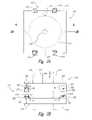
- FIG. 1Aillustrates a representative transfer molding tool 10 that simultaneously encases a plurality of microelectronic dies 60 .
- the molding tool 10can include an upper plate 30 removably positioned on a lower plate 20 to define a plurality of substrate chambers 14 .
- a plurality of channels 16connect the substrate chambers 14 to an upright pellet cylinder 17 .
- a cylindrical pellet 40 formed from an epoxy mold compoundis positioned in the cylinder 17 , and a plunger 15 moves upwardly within the cylinder 17 to transfer heat and exert pressure against the pellet 40 .
- the heat and pressure from the plunger 15liquefy the mold compound of the pellet 40 .
- the liquefied mold compoundflows through the channels 16 (as indicated by arrows F) and into the substrate chambers 14 to surround the microelectronic dies 60 .
- As the liquefied mold compound flows into the substrate chambers 114it drives out the air within the molding tool through small vents 18 . This is known as the transfer stage of the process.
- pressureis exerted on the encapsulant within the substrate chambers 14 to collapse microvoids that may be present within the encapsulant.
- the mold compound in the substrate chambers 14is then cooled and hardened to form a protective casing around each microelectronic die 60 .
- FIG. 1BAnother conventional technique for encapsulating dies is compression molding, illustrated schematically in FIG. 1B .
- the die 60is placed on a lower plate 20
- the encapsulant 40is placed on the die 60
- an upper plate 30is brought downwardly toward the lower plate 20 .
- the upper plate 30 and the lower plate 20together form a substrate chamber 14 .
- the amount of encapsulant 40 placed on the die 60is typically slightly more than is necessary to fully encapsulate the die 60 , so as to ensure complete encapsulation. Accordingly, the excess encapsulant 40 escapes from the substrate chamber 14 through escape channels 19 .
- wafer-level processing techniqueshave been used to at least partially encapsulate the dies at the wafer level.
- existing encapsulation techniqueshave been difficult to implement at the wafer level.
- the waferstypically include solder balls, wirebonds, or other conductive structures for connecting the dies to other devices.
- the rapid flow of encapsulant over the surface of the wafercan sweep away or otherwise disturb the position, shape and/or orientation of these conductive structures.
- the compression molding processcan also suffer from drawbacks. For example, when an encapsulant is disposed on a wafer having solder balls, wirebonds, or other small conductive structures, small pockets of air can be trapped between the encapsulant and the small conductive structures.
- the compression moldis not completely sealed (so as to allow excess mold compound to escape from the mold cavity via the escape channels 19 ), the encapsulant in the mold cavity cannot be compacted to collapse these voids. Therefore, for at least the foregoing reasons, it is desirable to improve the process for forming protective casings over microelectronic devices.
- FIG. 1Ais a partially schematic, cross-sectional side view of a molding apparatus for encapsulating microelectronic devices using a transfer mold process in accordance with the prior art.
- FIG. 1Bis a partially schematic, cross-sectional side view of a molding apparatus for encapsulating microelectronic devices using a compression process in accordance with the prior art.
- FIG. 2Ais a partially schematic, top view of a tool for encapsulating semiconductor workpieces in accordance with an embodiment of the invention.
- FIG. 2Bis a partially schematic, cross-sectional side view of the tool shown in FIG. 2A .
- FIG. 3is a partially schematic, cross-sectional side view of the tool shown in FIG. 2B with a semiconductor workpiece positioned for encapsulation in accordance with an embodiment of the invention.
- FIG. 4is a partially schematic, cross-sectional side view of the tool shown in FIG. 3 with an encapsulant disposed adjacent to the workpiece in accordance with an embodiment of the invention.
- FIG. 5is a partially schematic, cross-sectional side view of the tool shown in FIG. 4 with the encapsulant distributed over the workpiece in accordance with an embodiment of the invention.
- FIG. 6is a partially schematic, cross-sectional side view of the tool and the workpiece after the encapsulant has been compressed and excess encapsulant has been removed in accordance with an embodiment of the invention.
- FIG. 7is a partially schematic, cross-sectional side view of a tool configured to remove excess encapsulant in accordance with another embodiment of the invention.
- FIG. 8is an enlarged, partially schematic, cross-sectional side view of the workpiece shown in FIGS. 6 and 7 , illustrating a void collapsed in accordance with an embodiment of the invention.
- the workpiecescan include micromechanical components, data storage elements, optics, read/write components, or other features.
- the workpiecescan include wafers having dies including SRAM, DRAM (e.g., DDR-SDRAM), flash-memory (e.g., NAND flash-memory), processor, imager, and other dies.
- DRAMe.g., DDR-SDRAM
- flash-memorye.g., NAND flash-memory
- processorimager
- imagere.g., imager, and other dies.
- several other embodiments of the inventioncan have configurations, components, or procedures different than those described in this section. A person of ordinary skill in the art, therefore, will accordingly understand that the invention may have other embodiments with additional elements, or the invention may have other embodiments without several of the elements shown and described below with reference to FIG. 2A-8 .
- a particular method for encapsulating a semiconductor workpieceincludes placing the workpiece and an encapsulant in a mold cavity and driving some of the encapsulant from the mold cavity to an overflow chamber.
- the methodcan further include applying pressure to the encapsulant in the mold cavity via pressure applied to the encapsulant in the overflow chamber.
- a representative apparatus suitable for conducting such a methodincludes a mold element bounding a mold cavity that is positioned to receive a semiconductor workpiece and an encapsulant.
- the apparatusfurther includes an overflow chamber in flow communication with the mold cavity.
- a first pressurizing deviceis coupled to the mold cavity.
- a second pressurizing deviceis operatively coupled to the overflow chamber and, via the overflow chamber, the mold cavity.
- the first pressurizing devicecan pressurize the mold cavity to distribute the encapsulant adjacent the workpiece and drive excess encapsulant into the overflow chamber.
- the second pressurizing devicecan then pressurize the encapsulant, e.g., to reduce or eliminate microvoids.
- FIG. 2Ais a partially schematic top view of a tool 110 for processing semiconductor workpieces in accordance with one embodiment of the disclosure.
- the illustrated tool 110includes a mold 111 having a mold cavity 114 that houses the workpiece.
- One or more overflow chambers 121can be positioned around the periphery of the mold cavity 114 , in flow communication with the mold cavity 114 so as to receive some of the encapsulant placed in the mold cavity 114 .
- a mold actuator 115can drive one part of the mold 111 relative to another. Accordingly, the driven part of the mold 111 can operate as the first pressurizing device described above.
- a guide structure 112(shown schematically) can include one or more guide elements 113 that align the motion of the mold components.
- FIG. 2Bschematically illustrates a cross-sectional side view of the tool 110 shown in FIG. 2A .
- the mold 111includes a first mold element 120 and a second mold element 130 , with the mold cavity 114 defined at least in part by one or both of the mold elements 120 , 130 .
- the second mold element 130is driven by the mold actuator 115 toward and away from the first mold element 120 , as indicated by arrow A.
- the second mold element 130also houses the overflow chambers 121 , each of which includes an overflow piston 122 coupled to an overflow actuator 123 that drives the overflow piston 122 as indicated by arrows B. Accordingly, the overflow piston 122 can operate as the second pressurizing device described above.
- the first mold element 120can also include (optional) flash receptacles 131 that are aligned with the overflow chambers 121 .
- Each flash receptacle 131can include a flash piston 132 coupled to a flash actuator 133 , which drives the flash piston 132 as indicated by arrow C.
- a semiconductor workpiece and encapsulantare placed in the mold cavity 114 .
- the mold actuator 115drives the second mold element 130 toward the first mold element 120 to distribute the encapsulant and force some of the encapsulant into the overflow chambers 121 .
- the overflow pistons 122are then actuated to pressurize the encapsulant in the overflow chambers 121 , which in turn pressurizes the encapsulant in the mold cavity 114 .
- the overflow piston 122 and the flash piston 132are then used to separate flash in the overflow chambers 121 from the encapsulated workpiece in the mold cavity 114 . Further details of this process are described below with reference to FIGS. 3-8 .
- FIG. 3illustrates the tool 110 as it is prepared for an encapsulation process conducted in accordance with an embodiment of the invention.
- a first or lower releasable film 125is disposed adjacent to a first surface 124 of the first mold element 120
- a corresponding second or upper film 135is disposed adjacent a second surface 134 of the second mold element 130 .
- a semiconductor workpiece 160is positioned adjacent to the lower film 125 .
- the semiconductor workpiece 160 shown in FIG. 3is a wafer, e.g., a 100 mm, 200 mm, 300 mm, or other size wafer.
- the semiconductor workpiece 160can include dies singulated from such a wafer, or the semiconductor workpiece 160 can include other semiconductor structures.
- the overflow chamber 121 and the flash receptacle 131are closed prior to the encapsulation process. Accordingly, the overflow actuator 123 drives the overflow piston 122 so that it is positioned against the upper film 135 .
- the flash actuator 133drives the flash piston 132 so that it is positioned against the lower film 125 .
- a volume of encapsulant 140has been placed on the semiconductor workpiece 160 within the mold cavity 114 .
- the encapsulant 140can be placed on the semiconductor workpiece 160 after the workpiece 160 is placed in the mold cavity 114 , or the encapsulant 140 can be placed on the semiconductor workpiece 160 prior to positioning the workpiece 160 and the encapsulant together in the mold cavity 114 . In either arrangement, a sufficient amount of encapsulant 140 is placed in the mold cavity 114 to provide the desired coating thickness over the workpiece 160 , plus at least some excess encapsulant to ensure that the target surface (or surfaces) of the workpiece 160 facing away from the first mold element 120 are completely covered. In a particular embodiment, the upwardly facing surface of the workpiece 160 shown in FIG.
- the second mold element 130is then moved toward the first mold element 120 , as indicated by arrow A 1 .
- the first mold element 120can be driven toward the second mold element 130 , or both mold elements 120 , 130 can be driven toward each other.
- FIG. 5illustrates the tool 110 after the second mold element 130 has moved to its furthest extent toward the first mold element 120 , as indicated by arrow A 1 .
- the motion of the second mold element 130is halted by a stop 150 .
- the stop 150includes a first feature 151 carried by the first mold element 120 , and a second feature 152 carried by the second mold element 130 .
- the first and second features 151 , 152contact and/or engage each other to prevent further relative motion between the first mold element 120 and the second mold element 130 .
- the first feature 151 and the second feature 152include flat, bearing surfaces of the first mold element 120 and the second mold element 130 , respectively, covered by the first film 125 and the second film 135 , respectively.
- the first and second features 151 , 152can include other structures, and can be carried by structures other than the first mold element 120 and the second mold element 130 .
- one of the first and second features 151 , 152can be carried by the guide structure 112 .
- the portions of the first and second films 125 , 135 at the outer edges of the mold 111can press against each other, forming a tight seal that prevents egress of the encapsulant 140 .
- the second mold element 130moves toward the first mold element 120 , it contacts the flowable encapsulant 140 and distributes the encapsulant 140 over the workpiece 160 . It also drives at least some of the encapsulant 140 outwardly through flow communication channels or ports 116 (positioned between the second mold element 130 and the first mold element 120 ), and into the overflow chambers 121 . As the encapsulant 140 is driven outwardly, a portion of the encapsulant (e.g., a workpiece encapsulant 141 ) remains in the mold cavity 114 , and other portions (e.g., overflow encapsulant 142 ) enter the overflow chambers 121 .
- a portion of the encapsulante.g., a workpiece encapsulant 141
- other portionse.g., overflow encapsulant 142
- the overflow encapsulant 142As the overflow encapsulant 142 enters the overflow chambers 121 , it drives the overflow pistons 122 upwardly, as indicated by arrow B 1 , thereby increasing the volumes of overflow chambers 121 accessible to the encapsulant 140 .
- the overflow actuators 123can be driven so as to assist the motion of the overflow pistons 122 .
- the overflow actuators 123are disengaged or otherwise configured so as not to restrict the motion of the overflow pistons 122 . Accordingly, the force provided by the overflow encapsulant 142 drives the overflow pistons 122 upwardly.
- the flash pistons 132can remain in the position shown in FIG. 5 so that the overflow encapsulant 142 enters only the overflow chambers 121 and not the flash chambers 131 .
- a spacing S between the first film 125 and the second film 135has a desired value corresponding to the combined thickness of the workpiece 160 and the overlying workpiece encapsulant 141 .
- the stop 150is accordingly arranged to repeatedly and consistently maintain the spacing S over many cycles so that the thickness of the workpiece encapsulant 141 remains consistent from one workpiece 160 to the next.
- the same mold 111can be used even if the characteristics of the semiconductor workpiece 160 change from one encapsulation process to another. For example, if the semiconductor workpiece 160 is missing certain dies (as is the case with a repopulated substrate), the same mold 111 can still be used, but with an additional amount of encapsulant 140 to account for the missing dies.
- the spacing Scan be adjusted (by adjusting the stop 150 ) to accommodate different workpieces 160 . For example, if the workpieces 160 include stacked dies, or for some other reason have an overall thickness that is greater or less than a particular “base” thickness, then the spacing S can be adjusted to accommodate the changed thickness.
- the workpiece encapsulant 141 within the mold cavity 114is pressurized or compacted.
- the compaction processis performed by the overflow pistons 122 .
- the overflow pistons 122are driven downwardly as indicated by arrows B 2 , which pressurizes the overflow encapsulant 142 .
- the pressurized overflow encapsulant 142in turn pressurizes the workpiece encapsulant 141 via the flow channels 116 .
- the overflow pistons 122move by only a very small amount while still generating a high pressure within the mold cavity 114 .
- the elevated pressure in the mold cavity 114can reduce or eliminate microvoids and/or other irregularities in the workpiece encapsulant 141 .
- the encapsulant 140e.g., both the workpiece encapsulant 141 and the overflow encapsulant 142 ) are cooled and/or cured or otherwise hardened prior to removing the encapsulated workpiece 160 from the mold 111 .
- FIG. 6illustrates a process for removing the overflow encapsulant 142 from the encapsulated workpiece 160 , and then removing the encapsulated workpiece 160 from the mold 111 .
- the overflow piston 122is driven downwardly (as indicated by arrow B 2 ) and the flash piston 132 is also either driven downwardly or allowed to move downwardly under the force provided by the overflow piston 121 , as indicated by arrow C 2 .
- This motionsevers the overflow encapsulant 142 (now solidified into flash 143 ) from the workpiece encapsulant 141 .
- the second mold element 130is moved away from the first mold element 120 , and the encapsulated workpiece 160 is removed from the mold cavity 114 .
- FIG. 7illustrates another arrangement for separating the overflow encapsulant 142 from the encapsulated semiconductor workpiece 160 .
- the mold cavity 114is bounded in part by a cavity piston 126 housed in the first mold element 120 .
- the lower film 125is accordingly disposed adjacent to the cavity piston 126 , which is shown in a recessed position in FIG. 7 .
- the mold actuator 115can move the second mold element 130 upwardly, as indicated by arrow A 2 , while the overflow pistons 122 move downwardly to maintain the overflow encapsulant 142 in a fixed position.
- the cavity piston 126can move upwardly as indicated by arrow D 2 , (e.g., following the motion of the second mold element 130 ) so that the semiconductor workpiece 160 and the workpiece encapsulant 141 move upwardly as a unit and are separated from the overflow encapsulant 142 .
- the cavity piston 126can also be used (in addition to or in lieu of the adjustable stop 150 described above) to adjust the volume of the mold cavity 114 prior to encapsulation, so as to accommodate semiconductor workpieces 160 having different thicknesses or other characteristics.
- FIG. 8is an enlarged illustration of a small portion of the workpiece 160 while it is in the mold cavity 114 , and after the encapsulant 140 has been compacted.
- the workpiece 160can include a solder ball 161 or other structure (e.g., conductive structure) that projects away from the workpiece 160 .
- a solder ball 161or other structure (e.g., conductive structure) that projects away from the workpiece 160 .
- the solder ball 161can be connected to a through wafer interconnect (TWI) formed in the workpiece 160 , or it can be connected to other conductive features of the workpiece 160 .
- TWIthrough wafer interconnect
- a void 162(e.g., a microvoid) may be present around the solder ball 161 .
- the solder ball 161projects outwardly from the encapsulant 140 and is pressed into the upper film 135 as the overlying encapsulant 140 spreads out. This arrangement allows at least part of the solder ball 161 to be free of the encapsulant 140 and accessible for electrical coupling to other structures after the encapsulation process is completed.
- the conductive structureincludes a solder ball, as shown in FIG. 8 .
- the conductive structureincludes other elements, for example, solder or other conductive material bumps, or wire bonds.
- the upper film 135 (and/or the lower film 125 )can be formed from a suitable flexible material, including polytetrafluoroethylene, and can have a thickness selected to produce the desired degree of exposure for the conductive structure.
- the conductive structureincludes a solder ball having a diameter of about 330 microns prior to reflow, and about 277 microns after reflow
- the upper film 135can have a thickness of about 200-250 microns, which is thicker than conventional release films, so as to accommodate the solder ball.
- the foregoing dimensionscan have other values in other embodiments.
- encapsulation processplacing the encapsulant on the semiconductor workpiece and then pressing the encapsulant to distribute it over the workpiece can be less likely to disrupt the integrity of solder balls or other structures than forcing the encapsulant over the workpiece in a conventional transfer mold process.
- the velocity of the encapsulant as it is pressed and distributed over the workpiececan be significantly less than the velocity of an encapsulant that is injected into a fixed shape mold cavity and around the workpiece.
- subsequently pressurizing the encapsulantcan reduce microvoids or other discontinuities more effectively than can a conventional compression mold process.
- a cavity liner or filmthat receives portions of the conductive structures carried by the workpiece during an encapsulation process.
- This arrangementcan allow the conductive structures to project outwardly from the encapsulant, without interfering with the coverage provided by the encapsulant over the surface of the workpiece.
- the portions of the conductive structurescan therefore remain accessible for electrical connections to the workpiece after the encapsulated workpiece is removed from the mold.
- the cavity linercan also protect the surfaces of the mold from contaminants, e.g., to increase the lifespan of the mold and/or decrease the frequency with which the mold surfaces must be cleaned or otherwise serviced.
- the upper moldis shown in the Figures as being movable relative to the lower mold, but in other embodiments, the lower mold can be movable relative to the upper mold, or both molds can be movable relative to each other.
- the encapsulantis shown as being disposed above the semiconductor workpiece in the Figures, but in other embodiments, the workpiece can be disposed above the encapsulant, for example, if the encapsulant includes a powder encapsulant.
- the workpiece and the mold cavitycan have shapes other than those shown in the Figures and described above.
- the overflow chamberscan also have different sizes, configurations, numbers and/or arrangements, depending upon features including, but not limited to, the size and shape of the mold cavity.
- the overflow chamberscan be positioned in either one or both of the first and second mold portions.
- Devices other than pistonse.g., pressurized bladders
- pressurized bladderscan be used to pressurize the overflow encapsulant.
- such a bladdercan be pressurized by a piston located remotely from the overflow chamber.
Landscapes
- Engineering & Computer Science (AREA)
- Microelectronics & Electronic Packaging (AREA)
- Computer Hardware Design (AREA)
- Power Engineering (AREA)
- Physics & Mathematics (AREA)
- Condensed Matter Physics & Semiconductors (AREA)
- General Physics & Mathematics (AREA)
- Manufacturing & Machinery (AREA)
- Encapsulation Of And Coatings For Semiconductor Or Solid State Devices (AREA)
- Moulds For Moulding Plastics Or The Like (AREA)
Abstract
Description
- The present disclosure is related to systems and methods for compressing an encapsulant adjacent a semiconductor workpiece.
- Many packaged microelectronic devices have a substrate, a microelectronic die attached to the substrate, and a protective covering or encapsulant encasing the die. The protective covering is generally a plastic or epoxy compound that can be molded to form a casing over the die. The microelectronic die can be a memory device, a microprocessor, or another type of microelectronic assembly having integrated circuitry. Several types of packaged devices also include bond pads on the substrate that are coupled to the integrated circuitry of the die. The bond pads may alternatively be coupled to pins or other types of terminals that are exposed on the exterior of the microelectronic device for connecting the die to buses, circuits, and/or other microelectronic assemblies.
- A significant limiting process when manufacturing packaged microelectronic devices is encapsulating the die with the protective covering. The dies are sensitive components that should be protected from physical contact and potentially harmful environmental conditions to avoid damaging the die. The protective casing encapsulating the die, therefore, should seal the die from the external environment and shield the die from electrical and mechanical shocks. Thus, the protective casing should not have any voids that may allow contaminants or other harmful agents to contact and potentially damage the die.
- One conventional technique for encapsulating dies is known as transfer molding, and involves placing the die in a cavity of a mold and then injecting a thermoset material into the cavity.
FIG. 1A illustrates a representativetransfer molding tool 10 that simultaneously encases a plurality of microelectronic dies60. More specifically, themolding tool 10 can include anupper plate 30 removably positioned on alower plate 20 to define a plurality ofsubstrate chambers 14. A plurality ofchannels 16 connect thesubstrate chambers 14 to anupright pellet cylinder 17. Acylindrical pellet 40 formed from an epoxy mold compound is positioned in thecylinder 17, and aplunger 15 moves upwardly within thecylinder 17 to transfer heat and exert pressure against thepellet 40. The heat and pressure from theplunger 15 liquefy the mold compound of thepellet 40. The liquefied mold compound flows through the channels16 (as indicated by arrows F) and into thesubstrate chambers 14 to surround the microelectronic dies60. As the liquefied mold compound flows into thesubstrate chambers 114, it drives out the air within the molding tool throughsmall vents 18. This is known as the transfer stage of the process. During a subsequent compaction stage, pressure is exerted on the encapsulant within thesubstrate chambers 14 to collapse microvoids that may be present within the encapsulant. The mold compound in thesubstrate chambers 14 is then cooled and hardened to form a protective casing around eachmicroelectronic die 60. - Another conventional technique for encapsulating dies is compression molding, illustrated schematically in
FIG. 1B . During a compression molding process, thedie 60 is placed on alower plate 20, theencapsulant 40 is placed on thedie 60, and anupper plate 30 is brought downwardly toward thelower plate 20. Theupper plate 30 and thelower plate 20 together form asubstrate chamber 14. As theupper plate 30 contacts theencapsulant 40, it forces the encapsulant40 around the die60. The amount ofencapsulant 40 placed on the die60 is typically slightly more than is necessary to fully encapsulate the die60, so as to ensure complete encapsulation. Accordingly, the excess encapsulant40 escapes from thesubstrate chamber 14 throughescape channels 19. - As part of a continuing effort to streamline the process for manufacturing microelectronic devices, many processes which formerly were performed on singulated microelectronic dies are now being performed on unsingulated dies, including entire wafers of such dies. These processes are typically referred to as wafer-level processing techniques. In some cases, wafer-level processing has been used to at least partially encapsulate the dies at the wafer level. However, existing encapsulation techniques have been difficult to implement at the wafer level. For example, the wafers typically include solder balls, wirebonds, or other conductive structures for connecting the dies to other devices. When a wafer containing such conductive structures is placed in a transfer mold, the rapid flow of encapsulant over the surface of the wafer can sweep away or otherwise disturb the position, shape and/or orientation of these conductive structures. The compression molding process can also suffer from drawbacks. For example, when an encapsulant is disposed on a wafer having solder balls, wirebonds, or other small conductive structures, small pockets of air can be trapped between the encapsulant and the small conductive structures. However, because the compression mold is not completely sealed (so as to allow excess mold compound to escape from the mold cavity via the escape channels19), the encapsulant in the mold cavity cannot be compacted to collapse these voids. Therefore, for at least the foregoing reasons, it is desirable to improve the process for forming protective casings over microelectronic devices.
FIG. 1A is a partially schematic, cross-sectional side view of a molding apparatus for encapsulating microelectronic devices using a transfer mold process in accordance with the prior art.FIG. 1B is a partially schematic, cross-sectional side view of a molding apparatus for encapsulating microelectronic devices using a compression process in accordance with the prior art.FIG. 2A is a partially schematic, top view of a tool for encapsulating semiconductor workpieces in accordance with an embodiment of the invention.FIG. 2B is a partially schematic, cross-sectional side view of the tool shown inFIG. 2A .FIG. 3 is a partially schematic, cross-sectional side view of the tool shown inFIG. 2B with a semiconductor workpiece positioned for encapsulation in accordance with an embodiment of the invention.FIG. 4 is a partially schematic, cross-sectional side view of the tool shown inFIG. 3 with an encapsulant disposed adjacent to the workpiece in accordance with an embodiment of the invention.FIG. 5 is a partially schematic, cross-sectional side view of the tool shown inFIG. 4 with the encapsulant distributed over the workpiece in accordance with an embodiment of the invention.FIG. 6 is a partially schematic, cross-sectional side view of the tool and the workpiece after the encapsulant has been compressed and excess encapsulant has been removed in accordance with an embodiment of the invention.FIG. 7 is a partially schematic, cross-sectional side view of a tool configured to remove excess encapsulant in accordance with another embodiment of the invention.FIG. 8 is an enlarged, partially schematic, cross-sectional side view of the workpiece shown inFIGS. 6 and 7 , illustrating a void collapsed in accordance with an embodiment of the invention.- Specific details of several embodiments of the disclosure are described below with reference to semiconductor workpieces and systems for processing the workpieces. The workpieces can include micromechanical components, data storage elements, optics, read/write components, or other features. For example, the workpieces can include wafers having dies including SRAM, DRAM (e.g., DDR-SDRAM), flash-memory (e.g., NAND flash-memory), processor, imager, and other dies. Moreover, several other embodiments of the invention can have configurations, components, or procedures different than those described in this section. A person of ordinary skill in the art, therefore, will accordingly understand that the invention may have other embodiments with additional elements, or the invention may have other embodiments without several of the elements shown and described below with reference to
FIG. 2A-8 . - A particular method for encapsulating a semiconductor workpiece includes placing the workpiece and an encapsulant in a mold cavity and driving some of the encapsulant from the mold cavity to an overflow chamber. The method can further include applying pressure to the encapsulant in the mold cavity via pressure applied to the encapsulant in the overflow chamber. A representative apparatus suitable for conducting such a method includes a mold element bounding a mold cavity that is positioned to receive a semiconductor workpiece and an encapsulant. The apparatus further includes an overflow chamber in flow communication with the mold cavity. A first pressurizing device is coupled to the mold cavity. A second pressurizing device is operatively coupled to the overflow chamber and, via the overflow chamber, the mold cavity. Accordingly, the first pressurizing device can pressurize the mold cavity to distribute the encapsulant adjacent the workpiece and drive excess encapsulant into the overflow chamber. The second pressurizing device can then pressurize the encapsulant, e.g., to reduce or eliminate microvoids.
FIG. 2A is a partially schematic top view of atool 110 for processing semiconductor workpieces in accordance with one embodiment of the disclosure. The illustratedtool 110 includes amold 111 having amold cavity 114 that houses the workpiece. One ormore overflow chambers 121 can be positioned around the periphery of themold cavity 114, in flow communication with themold cavity 114 so as to receive some of the encapsulant placed in themold cavity 114. Amold actuator 115 can drive one part of themold 111 relative to another. Accordingly, the driven part of themold 111 can operate as the first pressurizing device described above. A guide structure112 (shown schematically) can include one ormore guide elements 113 that align the motion of the mold components.FIG. 2B schematically illustrates a cross-sectional side view of thetool 110 shown inFIG. 2A . As shown inFIG. 2B , themold 111 includes afirst mold element 120 and asecond mold element 130, with themold cavity 114 defined at least in part by one or both of themold elements second mold element 130 is driven by themold actuator 115 toward and away from thefirst mold element 120, as indicated by arrow A. Thesecond mold element 130 also houses theoverflow chambers 121, each of which includes anoverflow piston 122 coupled to anoverflow actuator 123 that drives theoverflow piston 122 as indicated by arrows B. Accordingly, theoverflow piston 122 can operate as the second pressurizing device described above.- The
first mold element 120 can also include (optional)flash receptacles 131 that are aligned with theoverflow chambers 121. Eachflash receptacle 131 can include aflash piston 132 coupled to aflash actuator 133, which drives theflash piston 132 as indicated by arrow C. In operation, a semiconductor workpiece and encapsulant are placed in themold cavity 114. Themold actuator 115 drives thesecond mold element 130 toward thefirst mold element 120 to distribute the encapsulant and force some of the encapsulant into theoverflow chambers 121. Theoverflow pistons 122 are then actuated to pressurize the encapsulant in theoverflow chambers 121, which in turn pressurizes the encapsulant in themold cavity 114. Optionally, theoverflow piston 122 and theflash piston 132 are then used to separate flash in theoverflow chambers 121 from the encapsulated workpiece in themold cavity 114. Further details of this process are described below with reference toFIGS. 3-8 . FIG. 3 illustrates thetool 110 as it is prepared for an encapsulation process conducted in accordance with an embodiment of the invention. A first or lowerreleasable film 125 is disposed adjacent to afirst surface 124 of thefirst mold element 120, and a corresponding second orupper film 135 is disposed adjacent asecond surface 134 of thesecond mold element 130. Asemiconductor workpiece 160 is positioned adjacent to thelower film 125. For purposes of illustration, thesemiconductor workpiece 160 shown inFIG. 3 is a wafer, e.g., a 100 mm, 200 mm, 300 mm, or other size wafer. In other embodiments, thesemiconductor workpiece 160 can include dies singulated from such a wafer, or thesemiconductor workpiece 160 can include other semiconductor structures.- The
overflow chamber 121 and theflash receptacle 131 are closed prior to the encapsulation process. Accordingly, theoverflow actuator 123 drives theoverflow piston 122 so that it is positioned against theupper film 135. Theflash actuator 133 drives theflash piston 132 so that it is positioned against thelower film 125. - In
FIG. 4 , a volume ofencapsulant 140 has been placed on thesemiconductor workpiece 160 within themold cavity 114. Theencapsulant 140 can be placed on thesemiconductor workpiece 160 after theworkpiece 160 is placed in themold cavity 114, or theencapsulant 140 can be placed on thesemiconductor workpiece 160 prior to positioning theworkpiece 160 and the encapsulant together in themold cavity 114. In either arrangement, a sufficient amount ofencapsulant 140 is placed in themold cavity 114 to provide the desired coating thickness over theworkpiece 160, plus at least some excess encapsulant to ensure that the target surface (or surfaces) of theworkpiece 160 facing away from thefirst mold element 120 are completely covered. In a particular embodiment, the upwardly facing surface of theworkpiece 160 shown inFIG. 4 is the target surface, and the sides and downwardly facing surface are protected from exposure to theencapsulant 140 by the lowerreleasable film 125. In other embodiments, these surfaces may also be encapsulated. Thesecond mold element 130 is then moved toward thefirst mold element 120, as indicated by arrow A1. Of course, it will be understood that in other embodiments, thefirst mold element 120 can be driven toward thesecond mold element 130, or bothmold elements FIG. 5 illustrates thetool 110 after thesecond mold element 130 has moved to its furthest extent toward thefirst mold element 120, as indicated by arrow A1. In this position, the motion of thesecond mold element 130 is halted by astop 150. In a particular embodiment shown inFIG. 5 , thestop 150 includes afirst feature 151 carried by thefirst mold element 120, and asecond feature 152 carried by thesecond mold element 130. The first andsecond features first mold element 120 and thesecond mold element 130. In the illustrated embodiment, thefirst feature 151 and thesecond feature 152 include flat, bearing surfaces of thefirst mold element 120 and thesecond mold element 130, respectively, covered by thefirst film 125 and thesecond film 135, respectively. In other embodiments, the first andsecond features first mold element 120 and thesecond mold element 130. For example, one of the first andsecond features guide structure 112. In any of these embodiments, the portions of the first andsecond films mold 111 can press against each other, forming a tight seal that prevents egress of theencapsulant 140.- As the
second mold element 130 moves toward thefirst mold element 120, it contacts theflowable encapsulant 140 and distributes theencapsulant 140 over theworkpiece 160. It also drives at least some of theencapsulant 140 outwardly through flow communication channels or ports116 (positioned between thesecond mold element 130 and the first mold element120), and into theoverflow chambers 121. As theencapsulant 140 is driven outwardly, a portion of the encapsulant (e.g., a workpiece encapsulant141) remains in themold cavity 114, and other portions (e.g., overflow encapsulant142) enter theoverflow chambers 121. As theoverflow encapsulant 142 enters theoverflow chambers 121, it drives theoverflow pistons 122 upwardly, as indicated by arrow B1, thereby increasing the volumes ofoverflow chambers 121 accessible to theencapsulant 140. Optionally, theoverflow actuators 123 can be driven so as to assist the motion of theoverflow pistons 122. However, in at least one embodiment, theoverflow actuators 123 are disengaged or otherwise configured so as not to restrict the motion of theoverflow pistons 122. Accordingly, the force provided by theoverflow encapsulant 142 drives theoverflow pistons 122 upwardly. At the same time, theflash pistons 132 can remain in the position shown inFIG. 5 so that theoverflow encapsulant 142 enters only theoverflow chambers 121 and not theflash chambers 131. - When the relative motion between the
first mold element 120 and thesecond mold element 130 is halted by thestop 150, a spacing S between thefirst film 125 and thesecond film 135 has a desired value corresponding to the combined thickness of theworkpiece 160 and theoverlying workpiece encapsulant 141. Thestop 150 is accordingly arranged to repeatedly and consistently maintain the spacing S over many cycles so that the thickness of theworkpiece encapsulant 141 remains consistent from oneworkpiece 160 to the next. - With the spacing S fixed, the
same mold 111 can be used even if the characteristics of thesemiconductor workpiece 160 change from one encapsulation process to another. For example, if thesemiconductor workpiece 160 is missing certain dies (as is the case with a repopulated substrate), thesame mold 111 can still be used, but with an additional amount ofencapsulant 140 to account for the missing dies. In another arrangement, the spacing S can be adjusted (by adjusting the stop150) to accommodatedifferent workpieces 160. For example, if theworkpieces 160 include stacked dies, or for some other reason have an overall thickness that is greater or less than a particular “base” thickness, then the spacing S can be adjusted to accommodate the changed thickness. - After the
encapsulant 140 has been distributed over theworkpiece 160, and relative motion of the first andsecond mold elements workpiece encapsulant 141 within themold cavity 114 is pressurized or compacted. In the illustrated embodiment, the compaction process is performed by theoverflow pistons 122. Theoverflow pistons 122 are driven downwardly as indicated by arrows B2, which pressurizes theoverflow encapsulant 142. Thepressurized overflow encapsulant 142 in turn pressurizes theworkpiece encapsulant 141 via theflow channels 116. Because theencapsulant 140 is generally incompressible, theoverflow pistons 122 move by only a very small amount while still generating a high pressure within themold cavity 114. The elevated pressure in themold cavity 114 can reduce or eliminate microvoids and/or other irregularities in theworkpiece encapsulant 141. After the compaction process has been completed, the encapsulant140 (e.g., both theworkpiece encapsulant 141 and the overflow encapsulant142) are cooled and/or cured or otherwise hardened prior to removing the encapsulatedworkpiece 160 from themold 111. FIG. 6 illustrates a process for removing theoverflow encapsulant 142 from the encapsulatedworkpiece 160, and then removing the encapsulatedworkpiece 160 from themold 111. To remove theoverflow encapsulant 142, theoverflow piston 122 is driven downwardly (as indicated by arrow B2) and theflash piston 132 is also either driven downwardly or allowed to move downwardly under the force provided by theoverflow piston 121, as indicated by arrow C2. This motion severs the overflow encapsulant142 (now solidified into flash143) from theworkpiece encapsulant 141. After theflash 143 has been removed, thesecond mold element 130 is moved away from thefirst mold element 120, and the encapsulatedworkpiece 160 is removed from themold cavity 114.FIG. 7 illustrates another arrangement for separating theoverflow encapsulant 142 from the encapsulatedsemiconductor workpiece 160. In this arrangement, themold cavity 114 is bounded in part by acavity piston 126 housed in thefirst mold element 120. Thelower film 125 is accordingly disposed adjacent to thecavity piston 126, which is shown in a recessed position inFIG. 7 . After encapsulation, themold actuator 115 can move thesecond mold element 130 upwardly, as indicated by arrow A2, while theoverflow pistons 122 move downwardly to maintain theoverflow encapsulant 142 in a fixed position. At the same time, thecavity piston 126 can move upwardly as indicated by arrow D2, (e.g., following the motion of the second mold element130) so that thesemiconductor workpiece 160 and theworkpiece encapsulant 141 move upwardly as a unit and are separated from theoverflow encapsulant 142. Thecavity piston 126 can also be used (in addition to or in lieu of theadjustable stop 150 described above) to adjust the volume of themold cavity 114 prior to encapsulation, so as to accommodatesemiconductor workpieces 160 having different thicknesses or other characteristics.FIG. 8 is an enlarged illustration of a small portion of theworkpiece 160 while it is in themold cavity 114, and after theencapsulant 140 has been compacted. As shown inFIG. 8 , theworkpiece 160 can include asolder ball 161 or other structure (e.g., conductive structure) that projects away from theworkpiece 160. For purposes of illustration, only asingle solder ball 161 is shown inFIG. 8 , though it will be understood that theworkpiece 160 will typically includemany solder balls 161. Thesolder ball 161 can be connected to a through wafer interconnect (TWI) formed in theworkpiece 160, or it can be connected to other conductive features of theworkpiece 160. When theencapsulant 140 is initially disposed on theworkpiece 160, a void162 (e.g., a microvoid) may be present around thesolder ball 161. As thesecond mold element 130 is driven toward thefirst mold element 120, theencapsulant 140 is spread out over the surface of theworkpiece 160. In a particular arrangement, thesolder ball 161 projects outwardly from theencapsulant 140 and is pressed into theupper film 135 as the overlyingencapsulant 140 spreads out. This arrangement allows at least part of thesolder ball 161 to be free of theencapsulant 140 and accessible for electrical coupling to other structures after the encapsulation process is completed. Once the motion of thesecond mold element 130 is halted, pressure is applied to theencapsulant 140 via the overflow piston122 (FIG. 6 ) to collapse thevoid 162, thus reducing or eliminating the likelihood that the void will expand and burst or otherwise disrupt the integrity of the packagedworkpiece 160.- In particular embodiments, the conductive structure includes a solder ball, as shown in
FIG. 8 . In other embodiments, the conductive structure includes other elements, for example, solder or other conductive material bumps, or wire bonds. The upper film135 (and/or the lower film125) can be formed from a suitable flexible material, including polytetrafluoroethylene, and can have a thickness selected to produce the desired degree of exposure for the conductive structure. For example, when the conductive structure includes a solder ball having a diameter of about 330 microns prior to reflow, and about 277 microns after reflow, theupper film 135 can have a thickness of about 200-250 microns, which is thicker than conventional release films, so as to accommodate the solder ball. The foregoing dimensions can have other values in other embodiments. - Several features of at least some of the foregoing embodiments can improve the effectiveness and/or efficiency of the encapsulation process. For example, placing the encapsulant on the semiconductor workpiece and then pressing the encapsulant to distribute it over the workpiece can be less likely to disrupt the integrity of solder balls or other structures than forcing the encapsulant over the workpiece in a conventional transfer mold process. In particular, the velocity of the encapsulant as it is pressed and distributed over the workpiece can be significantly less than the velocity of an encapsulant that is injected into a fixed shape mold cavity and around the workpiece. In addition, subsequently pressurizing the encapsulant can reduce microvoids or other discontinuities more effectively than can a conventional compression mold process.
- Another feature of at least some of the foregoing embodiments is a cavity liner or film that receives portions of the conductive structures carried by the workpiece during an encapsulation process. This arrangement can allow the conductive structures to project outwardly from the encapsulant, without interfering with the coverage provided by the encapsulant over the surface of the workpiece. The portions of the conductive structures can therefore remain accessible for electrical connections to the workpiece after the encapsulated workpiece is removed from the mold. The cavity liner can also protect the surfaces of the mold from contaminants, e.g., to increase the lifespan of the mold and/or decrease the frequency with which the mold surfaces must be cleaned or otherwise serviced.
- From the foregoing, it will be appreciated that specific embodiments of the invention have been described herein for purposes of illustration, but that various modifications may be made without deviating from the invention. For example, the upper mold is shown in the Figures as being movable relative to the lower mold, but in other embodiments, the lower mold can be movable relative to the upper mold, or both molds can be movable relative to each other. The encapsulant is shown as being disposed above the semiconductor workpiece in the Figures, but in other embodiments, the workpiece can be disposed above the encapsulant, for example, if the encapsulant includes a powder encapsulant. The workpiece and the mold cavity can have shapes other than those shown in the Figures and described above. The overflow chambers can also have different sizes, configurations, numbers and/or arrangements, depending upon features including, but not limited to, the size and shape of the mold cavity. The overflow chambers can be positioned in either one or both of the first and second mold portions. Devices other than pistons (e.g., pressurized bladders) can be used to pressurize the overflow encapsulant. Alternatively, such a bladder can be pressurized by a piston located remotely from the overflow chamber.
- Certain aspects of the invention described in the context of particular embodiments may be combined or eliminated in other embodiments. For example, characteristics of the encapsulation process described above with reference to
FIGS. 1-5 may be used in conjunction with the flash separation process described with reference toFIG. 7 . While the aspect of receiving portions of projecting structures (e.g., solder balls) in a flexible liner material was described in the context of the particular molding process shown in the Figures, this technique may be applied to other molding processes in other embodiments, for example, otherwise conventional compression mold or transfer mold processes. Further, while advantages associated with certain embodiments of the invention have been described in the context of those embodiments, other embodiments may also exhibit such advantages, and not all embodiments need necessarily exhibit such advantages to fall within the scope of the invention. Accordingly, the invention is not limited, except as by the appended claims.
Claims (48)
Priority Applications (3)
| Application Number | Priority Date | Filing Date | Title |
|---|---|---|---|
| US11/678,507US7833456B2 (en) | 2007-02-23 | 2007-02-23 | Systems and methods for compressing an encapsulant adjacent a semiconductor workpiece |
| PCT/US2008/054069WO2008103603A1 (en) | 2007-02-23 | 2008-02-15 | Systems and methods for compressing an encapsulant adjacent a semiconductor workpiece |
| TW097106280ATWI397133B (en) | 2007-02-23 | 2008-02-22 | Systems and methods for compressing an encapsulant adjacent a semiconductor workpiece |
Applications Claiming Priority (1)
| Application Number | Priority Date | Filing Date | Title |
|---|---|---|---|
| US11/678,507US7833456B2 (en) | 2007-02-23 | 2007-02-23 | Systems and methods for compressing an encapsulant adjacent a semiconductor workpiece |
Publications (2)
| Publication Number | Publication Date |
|---|---|
| US20080206930A1true US20080206930A1 (en) | 2008-08-28 |
| US7833456B2 US7833456B2 (en) | 2010-11-16 |
Family
ID=39445808
Family Applications (1)
| Application Number | Title | Priority Date | Filing Date |
|---|---|---|---|
| US11/678,507Active2029-03-18US7833456B2 (en) | 2007-02-23 | 2007-02-23 | Systems and methods for compressing an encapsulant adjacent a semiconductor workpiece |
Country Status (3)
| Country | Link |
|---|---|
| US (1) | US7833456B2 (en) |
| TW (1) | TWI397133B (en) |
| WO (1) | WO2008103603A1 (en) |
Cited By (9)
| Publication number | Priority date | Publication date | Assignee | Title |
|---|---|---|---|---|
| US8148210B1 (en)* | 2010-09-13 | 2012-04-03 | Infineon Technologies Ag | Method for fabricating a semiconductor chip panel |
| US9910460B2 (en)* | 2014-11-12 | 2018-03-06 | Apple Inc. | Micro-perforation overmolding gate |
| WO2018139631A1 (en)* | 2017-01-30 | 2018-08-02 | 信越エンジニアリング株式会社 | Resin sealing device and resin sealing method |
| US10163804B2 (en)* | 2013-12-18 | 2018-12-25 | Taiwan Semiconductor Manufacturing Company | Molding structure for wafer level package |
| CN109689330A (en)* | 2016-11-29 | 2019-04-26 | 东和株式会社 | Compression molding apparatus, compression molding method, and manufacturing method of compression molded product |
| CN114571664A (en)* | 2022-02-28 | 2022-06-03 | 邵周明 | Flash removing device and method for semiconductor chip packaging |
| US11621181B2 (en)* | 2020-05-05 | 2023-04-04 | Asmpt Singapore Pte. Ltd. | Dual-sided molding for encapsulating electronic devices |
| TWI822159B (en)* | 2022-06-30 | 2023-11-11 | 萬潤科技股份有限公司 | Pressing device and pressing equipment |
| EP4549121A1 (en)* | 2023-11-02 | 2025-05-07 | INTEL Corporation | Molding system and molding method |
Families Citing this family (9)
| Publication number | Priority date | Publication date | Assignee | Title |
|---|---|---|---|---|
| WO2010056212A2 (en)* | 2008-11-17 | 2010-05-20 | Pyxis Systems Integration Pte Ltd | Method for encapsulating semiconductor dies |
| JP5672652B2 (en)* | 2009-03-17 | 2015-02-18 | 凸版印刷株式会社 | Semiconductor element substrate manufacturing method and semiconductor device |
| CH703121B1 (en)* | 2010-05-10 | 2014-05-15 | Weidmann Plastics Tech Ag | A method for producing a prepared a sheet-like electronic element having plastic container, plastic container according to this method, as well as injection molding tool for carrying out the method. |
| TWI413195B (en)* | 2011-01-20 | 2013-10-21 | Walton Advanced Eng Inc | Method and apparatus of compression molding for reducing viods in molding compound |
| US8592970B2 (en)* | 2011-06-27 | 2013-11-26 | International Business Machines Corporation | Multichip electronic packages and methods of manufacture |
| US9731464B2 (en) | 2011-08-10 | 2017-08-15 | Nike, Inc. | Article of footwear formed from two preforms and method and mold for manufacturing same |
| US9096028B2 (en)* | 2011-08-10 | 2015-08-04 | Nike, Inc. | Article of footwear formed from two preforms and method and mold for manufacturing same |
| US8906743B2 (en)* | 2013-01-11 | 2014-12-09 | Micron Technology, Inc. | Semiconductor device with molded casing and package interconnect extending therethrough, and associated systems, devices, and methods |
| US9840432B2 (en)* | 2013-10-14 | 2017-12-12 | United Technologies Corporation | Assembly and method for transfer molding |
Citations (94)
| Publication number | Priority date | Publication date | Assignee | Title |
|---|---|---|---|---|
| US3672046A (en)* | 1970-01-14 | 1972-06-27 | Technitrol Inc | The method of making an electrical component |
| US4012307A (en)* | 1975-12-05 | 1977-03-15 | General Dynamics Corporation | Method for conditioning drilled holes in multilayer wiring boards |
| US4569814A (en)* | 1984-07-03 | 1986-02-11 | Motorola, Inc. | Preforming of preheated plastic pellets for use in transfer molding |
| US4814137A (en)* | 1988-02-16 | 1989-03-21 | Westinghouse Electric Corp. | High performance reliability fuel pellet |
| US4996587A (en)* | 1989-04-10 | 1991-02-26 | International Business Machines Corporation | Integrated semiconductor chip package |
| US5107328A (en)* | 1991-02-13 | 1992-04-21 | Micron Technology, Inc. | Packaging means for a semiconductor die having particular shelf structure |
| US5191174A (en)* | 1990-08-01 | 1993-03-02 | International Business Machines Corporation | High density circuit board and method of making same |
| US5192682A (en)* | 1990-05-10 | 1993-03-09 | Mitsubishi Denki Kabushiki Kaisha | Manufacturing method for thin semiconductor device assemblies |
| US5195023A (en)* | 1991-12-23 | 1993-03-16 | At&T Bell Laboratories | Integrated circuit package with strain relief grooves |
| US5197183A (en)* | 1991-11-05 | 1993-03-30 | Lsi Logic Corporation | Modified lead frame for reducing wire wash in transfer molding of IC packages |
| US5208467A (en)* | 1988-07-28 | 1993-05-04 | Semiconductor Energy Laboratory Co., Ltd. | Semiconductor device having a film-covered packaged component |
| US5296738A (en)* | 1991-07-08 | 1994-03-22 | Motorola, Inc. | Moisture relief for chip carrier |
| US5309026A (en)* | 1991-11-19 | 1994-05-03 | Nippon Precision Circuits Ltd. | Integrated circuit package having stress reducing recesses |
| US5314842A (en)* | 1988-09-30 | 1994-05-24 | Kabushiki Kaisha Toshiba | Resin-sealed type semiconductor device and method for manufacturing the same |
| US5527743A (en)* | 1993-08-18 | 1996-06-18 | Lsi Logic Corporation | Method for encapsulating an integrated circuit package |
| US5593927A (en)* | 1993-10-14 | 1997-01-14 | Micron Technology, Inc. | Method for packaging semiconductor dice |
| US5596231A (en)* | 1991-08-05 | 1997-01-21 | Asat, Limited | High power dissipation plastic encapsulated package for integrated circuit die |
| US5596321A (en)* | 1992-09-14 | 1997-01-21 | Koninklijke Ptt Nederland N.V. | System comprising a first encoder for coding a first digital signal, a second encoder for coding a second digital signal and at least one decoder for decoding coded digital signals, and coder and decoder for use in the system |
| US5606204A (en)* | 1994-06-23 | 1997-02-25 | Nec Corporation | Resin-sealed semiconductor device |
| US5609889A (en)* | 1995-05-26 | 1997-03-11 | Hestia Technologies, Inc. | Apparatus for encapsulating electronic packages |
| US5612576A (en)* | 1992-10-13 | 1997-03-18 | Motorola | Self-opening vent hole in an overmolded semiconductor device |
| US5635220A (en)* | 1994-09-22 | 1997-06-03 | Nec Corporation | Molding die for sealing semiconductor device with reduced resin burrs |
| US5710071A (en)* | 1995-12-04 | 1998-01-20 | Motorola, Inc. | Process for underfilling a flip-chip semiconductor device |
| US5721450A (en)* | 1995-06-12 | 1998-02-24 | Motorola, Inc. | Moisture relief for chip carriers |
| US5728600A (en)* | 1994-11-15 | 1998-03-17 | Vlt Corporation | Circuit encapsulation process |
| US5739585A (en)* | 1995-11-27 | 1998-04-14 | Micron Technology, Inc. | Single piece package for semiconductor die |
| US5750423A (en)* | 1995-08-25 | 1998-05-12 | Dai-Ichi Seiko Co., Ltd. | Method for encapsulation of semiconductor devices with resin and leadframe therefor |
| USD394844S (en)* | 1997-04-25 | 1998-06-02 | Micron Technology, Inc. | Temporary package for semiconductor dice |
| US5767446A (en)* | 1995-10-27 | 1998-06-16 | Anam Industrial Co., Ltd. | Printed circuit board having epoxy barrier around a throughout slot and ball grid array semiconductor package |
| US5766649A (en)* | 1995-12-15 | 1998-06-16 | Nec Corporation | Resin sealing mold die set with less resin remainder for semiconductor device |
| US5773322A (en)* | 1995-05-01 | 1998-06-30 | Lucent Technologies Inc. | Molded encapsulated electronic component |
| US5866953A (en)* | 1996-05-24 | 1999-02-02 | Micron Technology, Inc. | Packaged die on PCB with heat sink encapsulant |
| US5888443A (en)* | 1996-05-02 | 1999-03-30 | Texas Instruments Incorporated | Method for manufacturing prepackaged molding compound for component encapsulation |
| US5891753A (en)* | 1997-01-24 | 1999-04-06 | Micron Technology, Inc. | Method and apparatus for packaging flip chip bare die on printed circuit boards |
| US5893726A (en)* | 1997-12-15 | 1999-04-13 | Micron Technology, Inc. | Semiconductor package with pre-fabricated cover and method of fabrication |
| US5894167A (en)* | 1996-05-08 | 1999-04-13 | Micron Technology, Inc. | Encapsulant dam standoff for shell-enclosed die assemblies |
| US5917234A (en)* | 1994-12-09 | 1999-06-29 | Sony Corporation | Semiconductor device |
| US6013946A (en)* | 1996-09-11 | 2000-01-11 | Samsung Electronics Co., Ltd. | Wire bond packages for semiconductor chips and related methods and assemblies |
| US6015987A (en)* | 1993-08-05 | 2000-01-18 | Matsushita Electric Industrial Co., Ltd. | Semiconductor device having capacitor exhibiting improved mositure resistance and manufacturing method thereof |
| US6020629A (en)* | 1998-06-05 | 2000-02-01 | Micron Technology, Inc. | Stacked semiconductor package and method of fabrication |
| US6025728A (en)* | 1997-04-25 | 2000-02-15 | Micron Technology, Inc. | Semiconductor package with wire bond protective member |
| US6028365A (en)* | 1998-03-30 | 2000-02-22 | Micron Technology, Inc. | Integrated circuit package and method of fabrication |
| US6046496A (en)* | 1997-11-04 | 2000-04-04 | Micron Technology Inc | Chip package |
| US6049129A (en)* | 1997-12-19 | 2000-04-11 | Texas Instruments Incorporated | Chip size integrated circuit package |
| US6049125A (en)* | 1997-12-29 | 2000-04-11 | Micron Technology, Inc. | Semiconductor package with heat sink and method of fabrication |
| US6048744A (en)* | 1997-09-15 | 2000-04-11 | Micron Technology, Inc. | Integrated circuit package alignment feature |
| US6048755A (en)* | 1998-11-12 | 2000-04-11 | Micron Technology, Inc. | Method for fabricating BGA package using substrate with patterned solder mask open in die attach area |
| US6054755A (en)* | 1997-10-14 | 2000-04-25 | Sumitomo Metal (Smi) Electronics Devices Inc. | Semiconductor package with improved moisture vapor relief function and method of fabricating the same |
| US6063650A (en)* | 1996-01-11 | 2000-05-16 | Micron Technology, Inc. | Reduced stress LOC assembly |
| US6066514A (en)* | 1996-10-18 | 2000-05-23 | Micron Technology, Inc. | Adhesion enhanced semiconductor die for mold compound packaging |
| US6071758A (en)* | 1995-11-14 | 2000-06-06 | Sgs-Thomson Microelectronics S.A. | Process for manufacturing a chip card micromodule with protection barriers |
| US6072236A (en)* | 1996-03-07 | 2000-06-06 | Micron Technology, Inc. | Micromachined chip scale package |
| US6071457A (en)* | 1998-09-24 | 2000-06-06 | Texas Instruments Incorporated | Bellows container packaging system and method |
| US6075288A (en)* | 1998-06-08 | 2000-06-13 | Micron Technology, Inc. | Semiconductor package having interlocking heat sinks and method of fabrication |
| US6168970B1 (en)* | 1990-08-01 | 2001-01-02 | Staktek Group L.P. | Ultra high density integrated circuit packages |
| US6172419B1 (en)* | 1998-02-24 | 2001-01-09 | Micron Technology, Inc. | Low profile ball grid array package |
| US6172423B1 (en)* | 1997-11-15 | 2001-01-09 | Hyundai Electronics Industries Co., Ltd. | Layer-type ball grid array semiconductor package and fabrication method thereof |
| US6175159B1 (en)* | 1997-07-16 | 2001-01-16 | Oki Electric Industry Co., Ltd. | Semiconductor package |
| US6184465B1 (en)* | 1998-11-12 | 2001-02-06 | Micron Technology, Inc. | Semiconductor package |
| US6191472B1 (en)* | 1999-01-05 | 2001-02-20 | Intel Corporation | Hole geometry of a semiconductor package substrate |
| US6198172B1 (en)* | 1997-02-20 | 2001-03-06 | Micron Technology, Inc. | Semiconductor chip package |
| US6201299B1 (en)* | 1999-06-23 | 2001-03-13 | Advanced Semiconductor Engineering, Inc. | Substrate structure of BGA semiconductor package |
| US6203967B1 (en)* | 1998-07-31 | 2001-03-20 | Kulicke & Soffa Holdings, Inc. | Method for controlling stress in thin film layers deposited over a high density interconnect common circuit base |
| US6203319B1 (en)* | 1999-12-01 | 2001-03-20 | Edward Stanley Lee | Pellet-forming mold for dental filling materials |
| US6208519B1 (en)* | 1999-08-31 | 2001-03-27 | Micron Technology, Inc. | Thermally enhanced semiconductor package |
| US6210992B1 (en)* | 1999-08-31 | 2001-04-03 | Micron Technology, Inc. | Controlling packaging encapsulant leakage |
| US6218731B1 (en)* | 1999-05-21 | 2001-04-17 | Siliconware Precision Industries Co., Ltd. | Tiny ball grid array package |
| US6228687B1 (en)* | 1999-06-28 | 2001-05-08 | Micron Technology, Inc. | Wafer-level package and methods of fabricating |
| US6229202B1 (en)* | 2000-01-10 | 2001-05-08 | Micron Technology, Inc. | Semiconductor package having downset leadframe for reducing package bow |
| US6228548B1 (en)* | 1998-02-27 | 2001-05-08 | Micron Technology, Inc. | Method of making a multichip semiconductor package |
| US6235994B1 (en)* | 1998-06-29 | 2001-05-22 | International Business Machines Corporation | Thermal/electrical break for printed circuit boards |
| US6242802B1 (en)* | 1995-07-17 | 2001-06-05 | Motorola, Inc. | Moisture enhanced ball grid array package |
| US6251703B1 (en)* | 1998-12-14 | 2001-06-26 | Ela Medical S.A. | CMS coated microelectronic component and its method of manufacture |
| US6252298B1 (en)* | 1997-06-18 | 2001-06-26 | Samsung Electronics Co., Ltd. | Semiconductor chip package using flexible circuit board with central opening |
| US6338813B1 (en)* | 1999-10-15 | 2002-01-15 | Advanced Semiconductor Engineering, Inc. | Molding method for BGA semiconductor chip package |
| US20020006686A1 (en)* | 2000-07-12 | 2002-01-17 | Cloud Eugene H. | Die to die connection method and assemblies and packages including dice so connected |
| US6343019B1 (en)* | 1997-12-22 | 2002-01-29 | Micron Technology, Inc. | Apparatus and method of stacking die on a substrate |
| US6349582B2 (en)* | 1998-05-06 | 2002-02-26 | Komatsu, Ltd. | Die system for full enclosed die forging |
| US6385049B1 (en)* | 2001-07-05 | 2002-05-07 | Walsin Advanced Electronics Ltd | Multi-board BGA package |
| US6403009B1 (en)* | 1994-11-15 | 2002-06-11 | Vlt Corporation | Circuit encapsulation |
| US6503780B1 (en)* | 2000-07-05 | 2003-01-07 | Amkor Technology, Inc. | Wafer scale image sensor package fabrication method |
| US6525412B2 (en)* | 2000-11-30 | 2003-02-25 | Kabushiki Kaisha Toshiba | Semiconductor device having chip scale package |
| US6534861B1 (en)* | 1999-11-15 | 2003-03-18 | Substrate Technologies Incorporated | Ball grid substrate for lead-on-chip semiconductor package |
| US6549821B1 (en)* | 1999-02-26 | 2003-04-15 | Micron Technology, Inc. | Stereolithographic method and apparatus for packaging electronic components and resulting structures |
| US6558600B1 (en)* | 2000-05-04 | 2003-05-06 | Micron Technology, Inc. | Method for packaging microelectronic substrates |
| US6562278B1 (en)* | 2000-08-29 | 2003-05-13 | Micron Technology, Inc. | Methods of fabricating housing structures and micromachines incorporating such structures |
| US6677675B2 (en)* | 2000-06-16 | 2004-01-13 | Micron Technology, Inc. | Microelectronic devices and microelectronic die packages |
| US6688774B2 (en)* | 2001-06-12 | 2004-02-10 | Aktiebolaget Skf | Mounting means |
| US6734571B2 (en)* | 2001-01-23 | 2004-05-11 | Micron Technology, Inc. | Semiconductor assembly encapsulation mold |
| US20040101631A1 (en)* | 2002-11-26 | 2004-05-27 | Towa Corporation | Method of resin encapsulation, apparatus for resin encapsulation, method of manufacturing semiconductor device, semiconductor device and resin material |
| US6838760B1 (en)* | 2000-08-28 | 2005-01-04 | Micron Technology, Inc. | Packaged microelectronic devices with interconnecting units |
| US20050064065A1 (en)* | 2001-10-05 | 2005-03-24 | Seng Jimmy Chew Hwee | Apparatus for molding a semiconductor wafer and process therefor |
| US6982386B2 (en)* | 2000-08-23 | 2006-01-03 | Micron Technology, Inc. | Interconnecting substrates for electrical coupling of microelectronic components |
| US7049685B2 (en)* | 2000-08-24 | 2006-05-23 | Micron Technology, Inc. | Packaged microelectronic devices with pressure release elements and methods for manufacturing and using such packaged microelectronic devices |
Family Cites Families (117)
| Publication number | Priority date | Publication date | Assignee | Title |
|---|---|---|---|---|
| US4285780A (en) | 1978-11-02 | 1981-08-25 | Schachter Herbert I | Method of making a multi-level circuit board |
| US4473516A (en) | 1983-01-03 | 1984-09-25 | Hoover Universal, Inc. | Method and apparatus for injection molding plastic articles having solid exterior surfaces and porous interior cores |
| JPS60208847A (en) | 1984-04-02 | 1985-10-21 | Oki Electric Ind Co Ltd | Heat resisting plastic ic |
| JPS60257546A (en) | 1984-06-04 | 1985-12-19 | Mitsubishi Electric Corp | Semiconductor device and its manufacturing method |
| US4777520A (en) | 1986-03-27 | 1988-10-11 | Oki Electric Industry Co. Ltd. | Heat-resistant plastic semiconductor device |
| GB8609324D0 (en) | 1986-04-16 | 1986-05-21 | Micropore International Ltd | Enclosing object |
| IT1201836B (en) | 1986-07-17 | 1989-02-02 | Sgs Microelettronica Spa | SEMICONDUCTOR DEVICE MOUNTED IN A HIGHLY FLEXIBLE SEGMENTED CONTAINER AND PROVIDED WITH A THERMAL DISSIPATOR |
| US4882212A (en) | 1986-10-30 | 1989-11-21 | Olin Corporation | Electronic packaging of components incorporating a ceramic-glass-metal composite |
| US4855807A (en) | 1986-12-26 | 1989-08-08 | Kabushiki Kaisha Toshiba | Semiconductor device |
| USRE36469E (en) | 1988-09-30 | 1999-12-28 | Micron Technology, Inc. | Packaging for semiconductor logic devices |
| US5138434A (en) | 1991-01-22 | 1992-08-11 | Micron Technology, Inc. | Packaging for semiconductor logic devices |
| US5043199A (en) | 1988-10-31 | 1991-08-27 | Fujitsu Limited | Resin tablet for plastic encapsulation and method of manufacturing of plastic encapsulation using the resin tablet |
| EP0392042A1 (en) | 1989-04-11 | 1990-10-17 | Pfaudler Werke GmbH | Corrosion resistant enameled valve |
| US5344600A (en) | 1989-06-07 | 1994-09-06 | Motorola, Inc. | Method for encapsulating semiconductor devices with package bodies |
| JPH0423485A (en) | 1990-05-18 | 1992-01-27 | Cmk Corp | Printed wiring board and its manufacturing method |
| US5147821A (en) | 1990-09-28 | 1992-09-15 | Motorola, Inc. | Method for making a thermally enhanced semiconductor device by holding a leadframe against a heatsink through vacuum suction in a molding operation |
| FR2673017A1 (en) | 1991-02-18 | 1992-08-21 | Schlumberger Ind Sa | METHOD FOR MANUFACTURING AN ELECTRONIC MODULE FOR A MEMORY CARD AND ELECTRONIC MODULE THUS OBTAINED. |
| US5815000A (en) | 1991-06-04 | 1998-09-29 | Micron Technology, Inc. | Method for testing semiconductor dice with conventionally sized temporary packages |
| US5946553A (en) | 1991-06-04 | 1999-08-31 | Micron Technology, Inc. | Process for manufacturing a semiconductor package with bi-substrate die |
| US6094058A (en) | 1991-06-04 | 2000-07-25 | Micron Technology, Inc. | Temporary semiconductor package having dense array external contacts |
| US5128831A (en) | 1991-10-31 | 1992-07-07 | Micron Technology, Inc. | High-density electronic package comprising stacked sub-modules which are electrically interconnected by solder-filled vias |
| NL9200127A (en) | 1992-01-23 | 1993-08-16 | Ireneus Johannes Theodorus Mar | METHOD FOR PRESSING IN A MOLDING SECTION OF A PLASTIC CURED BY A REACTION, A PILLARED PRESSURE MATERIAL TO BE USED THEREIN AND A HOLDER OF SUCH MATERIALS |
| US5326243A (en) | 1992-06-25 | 1994-07-05 | Fierkens Richard H J | Compression-cavity mold for plastic encapsulation of thin-package integrated circuit device |
| US5363280A (en) | 1993-04-22 | 1994-11-08 | International Business Machines Corporation | Printed circuit board or card thermal mass design |
| US5474958A (en) | 1993-05-04 | 1995-12-12 | Motorola, Inc. | Method for making semiconductor device having no die supporting surface |
| TW222346B (en) | 1993-05-17 | 1994-04-11 | American Telephone & Telegraph | Method for packaging an electronic device substrate in a plastic encapsulant |
| US5958100A (en) | 1993-06-03 | 1999-09-28 | Micron Technology, Inc. | Process of making a glass semiconductor package |
| US5665281A (en) | 1993-12-02 | 1997-09-09 | Motorola, Inc. | Method for molding using venting pin |
| US5665296A (en) | 1994-03-24 | 1997-09-09 | Intel Corporation | Molding technique for molding plastic packages |
| US5449427A (en) | 1994-05-23 | 1995-09-12 | General Electric Company | Processing low dielectric constant materials for high speed electronics |
| US5964030A (en) | 1994-06-10 | 1999-10-12 | Vlsi Technology, Inc. | Mold flow regulating dam ring |
| US6046076A (en) | 1994-12-29 | 2000-04-04 | Tessera, Inc. | Vacuum dispense method for dispensing an encapsulant and machine therefor |
| US5976955A (en) | 1995-01-04 | 1999-11-02 | Micron Technology, Inc. | Packaging for bare dice employing EMR-sensitive adhesives |
| JPH08300397A (en) | 1995-05-01 | 1996-11-19 | Motorola Inc | Method and apparatus for transferring sealing material to cavity of mold |
| EP0742586A3 (en) | 1995-05-02 | 1998-03-11 | Texas Instruments Incorporated | Improvements in or relating to integrated circuits |
| US5677566A (en) | 1995-05-08 | 1997-10-14 | Micron Technology, Inc. | Semiconductor chip package |
| US5801073A (en) | 1995-05-25 | 1998-09-01 | Charles Stark Draper Laboratory | Net-shape ceramic processing for electronic devices and packages |
| US5696033A (en) | 1995-08-16 | 1997-12-09 | Micron Technology, Inc. | Method for packaging a semiconductor die |
| US5842275A (en) | 1995-09-05 | 1998-12-01 | Ford Motor Company | Reflow soldering to mounting pads with vent channels to avoid skewing |
| US5766987A (en)* | 1995-09-22 | 1998-06-16 | Tessera, Inc. | Microelectronic encapsulation methods and equipment |
| US5796159A (en) | 1995-11-30 | 1998-08-18 | Analog Devices, Inc. | Thermally efficient integrated circuit package |
| US5851845A (en) | 1995-12-18 | 1998-12-22 | Micron Technology, Inc. | Process for packaging a semiconductor die using dicing and testing |
| US5793613A (en) | 1995-12-29 | 1998-08-11 | Sgs-Thomson Microelectronics S.R.1. | Heat-dissipating and supporting structure for a plastic package with a fully insulated heat sink for an electronic device |
| US5817545A (en) | 1996-01-24 | 1998-10-06 | Cornell Research Foundation, Inc. | Pressurized underfill encapsulation of integrated circuits |
| US5723907A (en) | 1996-06-25 | 1998-03-03 | Micron Technology, Inc. | Loc simm |
| US5811879A (en) | 1996-06-26 | 1998-09-22 | Micron Technology, Inc. | Stacked leads-over-chip multi-chip module |
| EP0817261B1 (en) | 1996-06-28 | 2003-04-23 | STMicroelectronics S.r.l. | Method for manufacturing plastic package for electronic device having a fully insulated dissipator |
| US5938956A (en) | 1996-09-10 | 1999-08-17 | Micron Technology, Inc. | Circuit and method for heating an adhesive to package or rework a semiconductor die |
| JP3572833B2 (en) | 1996-12-19 | 2004-10-06 | 株式会社デンソー | Method for manufacturing resin-encapsulated semiconductor device |
| US6103547A (en) | 1997-01-17 | 2000-08-15 | Micron Technology, Inc. | High speed IC package configuration |
| US6100598A (en) | 1997-03-06 | 2000-08-08 | Nippon Steel Semiconductor Corporation | Sealed semiconductor device with positional deviation between upper and lower molds |
| USD402638S (en) | 1997-04-25 | 1998-12-15 | Micron Technology, Inc. | Temporary package for semiconductor dice |
| US6000603A (en)* | 1997-05-23 | 1999-12-14 | 3M Innovative Properties Company | Patterned array of metal balls and methods of making |
| US6159764A (en) | 1997-07-02 | 2000-12-12 | Micron Technology, Inc. | Varied-thickness heat sink for integrated circuit (IC) packages and method of fabricating IC packages |
| US5955777A (en) | 1997-07-02 | 1999-09-21 | Micron Technology, Inc. | Lead frame assemblies with voltage reference plane and IC packages including same |
| US5986209A (en) | 1997-07-09 | 1999-11-16 | Micron Technology, Inc. | Package stack via bottom leaded plastic (BLP) packaging |
| US6472252B2 (en) | 1997-07-23 | 2002-10-29 | Micron Technology, Inc. | Methods for ball grid array (BGA) encapsulation mold |
| US6107122A (en) | 1997-08-04 | 2000-08-22 | Micron Technology, Inc. | Direct die contact (DDC) semiconductor package |
| US6114189A (en) | 1997-09-10 | 2000-09-05 | Lsi Logic Corp. | Molded array integrated circuit package |
| JPH11121488A (en) | 1997-10-15 | 1999-04-30 | Toshiba Corp | Semiconductor device manufacturing method and resin sealing device |
| US6038136A (en) | 1997-10-29 | 2000-03-14 | Hestia Technologies, Inc. | Chip package with molded underfill |
| US6324069B1 (en) | 1997-10-29 | 2001-11-27 | Hestia Technologies, Inc. | Chip package with molded underfill |
| US6097087A (en) | 1997-10-31 | 2000-08-01 | Micron Technology, Inc. | Semiconductor package including flex circuit, interconnects and dense array external contacts |
| US5899705A (en) | 1997-11-20 | 1999-05-04 | Akram; Salman | Stacked leads-over chip multi-chip module |
| US6091157A (en) | 1997-12-05 | 2000-07-18 | Advanced Micro Devices, Inc. | Method to improve internal package delamination and wire bond reliability using non-homogeneous molding compound pellets |
| US5989941A (en) | 1997-12-12 | 1999-11-23 | Micron Technology, Inc. | Encapsulated integrated circuit packaging |
| US5994784A (en) | 1997-12-18 | 1999-11-30 | Micron Technology, Inc. | Die positioning in integrated circuit packaging |
| US5952611A (en) | 1997-12-19 | 1999-09-14 | Texas Instruments Incorporated | Flexible pin location integrated circuit package |
| US6117382A (en) | 1998-02-05 | 2000-09-12 | Micron Technology, Inc. | Method for encasing array packages |
| US6314639B1 (en) | 1998-02-23 | 2001-11-13 | Micron Technology, Inc. | Chip scale package with heat spreader and method of manufacture |
| JP3481117B2 (en) | 1998-02-25 | 2003-12-22 | 富士通株式会社 | Semiconductor device and manufacturing method thereof |
| US5933713A (en) | 1998-04-06 | 1999-08-03 | Micron Technology, Inc. | Method of forming overmolded chip scale package and resulting product |
| US6501157B1 (en) | 1998-04-15 | 2002-12-31 | Micron Technology, Inc. | Substrate for accepting wire bonded or flip-chip components |
| US6089920A (en) | 1998-05-04 | 2000-07-18 | Micron Technology, Inc. | Modular die sockets with flexible interconnects for packaging bare semiconductor die |
| US5990566A (en) | 1998-05-20 | 1999-11-23 | Micron Technology, Inc. | High density semiconductor package |
| US6008070A (en) | 1998-05-21 | 1999-12-28 | Micron Technology, Inc. | Wafer level fabrication and assembly of chip scale packages |
| US6215175B1 (en) | 1998-07-06 | 2001-04-10 | Micron Technology, Inc. | Semiconductor package having metal foil die mounting plate |
| US6100114A (en)* | 1998-08-10 | 2000-08-08 | International Business Machines Corporation | Encapsulation of solder bumps and solder connections |
| US6299053B1 (en) | 1998-08-19 | 2001-10-09 | Kulicke & Soffa Holdings, Inc. | Isolated flip chip or BGA to minimize interconnect stress due to thermal mismatch |
| US6124150A (en) | 1998-08-20 | 2000-09-26 | Micron Technology, Inc. | Transverse hybrid LOC package |
| US6153929A (en) | 1998-08-21 | 2000-11-28 | Micron Technology, Inc. | Low profile multi-IC package connector |
| US6291894B1 (en) | 1998-08-31 | 2001-09-18 | Micron Technology, Inc. | Method and apparatus for a semiconductor package for vertical surface mounting |
| US6326687B1 (en) | 1998-09-01 | 2001-12-04 | Micron Technology, Inc. | IC package with dual heat spreaders |
| US6515355B1 (en) | 1998-09-02 | 2003-02-04 | Micron Technology, Inc. | Passivation layer for packaged integrated circuits |
| US6117797A (en) | 1998-09-03 | 2000-09-12 | Micron Technology, Inc. | Attachment method for heat sinks and devices involving removal of misplaced encapsulant |
| US6084297A (en) | 1998-09-03 | 2000-07-04 | Micron Technology, Inc. | Cavity ball grid array apparatus |
| JP3421591B2 (en) | 1998-09-28 | 2003-06-30 | 三洋電機株式会社 | Manufacturing method of hybrid integrated circuit device |
| US6277671B1 (en) | 1998-10-20 | 2001-08-21 | Micron Technology, Inc. | Methods of forming integrated circuit packages |
| US6303985B1 (en) | 1998-11-12 | 2001-10-16 | Micron Technology, Inc. | Semiconductor lead frame and package with stiffened mounting paddle |
| JP2000150730A (en) | 1998-11-17 | 2000-05-30 | Fujitsu Ltd | Semiconductor device and manufacturing method thereof |
| US6143581A (en) | 1999-02-22 | 2000-11-07 | Micron Technology, Inc. | Asymmetric transfer molding method and an asymmetric encapsulation made therefrom |
| US6306331B1 (en) | 1999-03-24 | 2001-10-23 | International Business Machines Corporation | Ultra mold for encapsulating very thin packages |
| US6329603B1 (en) | 1999-04-07 | 2001-12-11 | International Business Machines Corporation | Low CTE power and ground planes |
| US6310390B1 (en) | 1999-04-08 | 2001-10-30 | Micron Technology, Inc. | BGA package and method of fabrication |
| US6268650B1 (en) | 1999-05-25 | 2001-07-31 | Micron Technology, Inc. | Semiconductor device, ball grid array connection system, and method of making |
| US6423470B1 (en) | 1999-08-20 | 2002-07-23 | 3M Innovative Properties Company | Printed circuit substrate with controlled placement covercoat layer |
| US6294839B1 (en) | 1999-08-30 | 2001-09-25 | Micron Technology, Inc. | Apparatus and methods of packaging and testing die |
| US6303981B1 (en) | 1999-09-01 | 2001-10-16 | Micron Technology, Inc. | Semiconductor package having stacked dice and leadframes and method of fabrication |
| JP4202549B2 (en) | 1999-09-01 | 2008-12-24 | Tdk株式会社 | Electrochemical device and manufacturing method thereof |
| JP2001085565A (en) | 1999-09-17 | 2001-03-30 | Hitachi Ltd | Semiconductor device and method of manufacturing the same |
| US6291884B1 (en) | 1999-11-09 | 2001-09-18 | Amkor Technology, Inc. | Chip-size semiconductor packages |
| US6309916B1 (en) | 1999-11-17 | 2001-10-30 | Amkor Technology, Inc | Method of molding plastic semiconductor packages |
| US6329220B1 (en) | 1999-11-23 | 2001-12-11 | Micron Technology, Inc. | Packages for semiconductor die |
| US6331453B1 (en) | 1999-12-16 | 2001-12-18 | Micron Technology, Inc. | Method for fabricating semiconductor packages using mold tooling fixture with flash control cavities |
| JP3971541B2 (en)* | 1999-12-24 | 2007-09-05 | 富士通株式会社 | Semiconductor device manufacturing method and split mold used in this method |
| US6531335B1 (en) | 2000-04-28 | 2003-03-11 | Micron Technology, Inc. | Interposers including upwardly protruding dams, semiconductor device assemblies including the interposers, and methods |
| US6413801B1 (en) | 2000-05-02 | 2002-07-02 | Advanced Semiconductor Engineering, Inc. | Method of molding semiconductor device and molding die for use therein |
| US6326698B1 (en) | 2000-06-08 | 2001-12-04 | Micron Technology, Inc. | Semiconductor devices having protective layers thereon through which contact pads are exposed and stereolithographic methods of fabricating such semiconductor devices |
| US6407381B1 (en) | 2000-07-05 | 2002-06-18 | Amkor Technology, Inc. | Wafer scale image sensor package |
| US6326700B1 (en) | 2000-08-15 | 2001-12-04 | United Test Center, Inc. | Low profile semiconductor package and process for making the same |
| US6462883B1 (en) | 2000-08-23 | 2002-10-08 | Apollo Instruments Inc. | Optical coupling systems |
| JP2002289741A (en)* | 2001-03-23 | 2002-10-04 | Nec Kyushu Ltd | Semiconductor device |
| US20030147185A1 (en) | 2002-02-01 | 2003-08-07 | Regala Mariano P. | Degater having movable support pins |
| SG127684A1 (en) | 2002-08-19 | 2006-12-29 | Micron Technology Inc | Packaged microelectronic component assemblies |
| US7153462B2 (en)* | 2004-04-23 | 2006-12-26 | Vishay Infrared Components, Inc. | Injection casting system for encapsulating semiconductor devices and method of use |
| US20060261498A1 (en) | 2005-05-17 | 2006-11-23 | Micron Technology, Inc. | Methods and apparatuses for encapsulating microelectronic devices |
| US7338842B2 (en)* | 2005-07-22 | 2008-03-04 | National Starch And Chemical Investment Holding Corporation | Process for exposing solder bumps on an underfill coated semiconductor |
- 2007
- 2007-02-23USUS11/678,507patent/US7833456B2/enactiveActive
- 2008
- 2008-02-15WOPCT/US2008/054069patent/WO2008103603A1/enactiveApplication Filing
- 2008-02-22TWTW097106280Apatent/TWI397133B/enactive
Patent Citations (99)
| Publication number | Priority date | Publication date | Assignee | Title |
|---|---|---|---|---|
| US3672046A (en)* | 1970-01-14 | 1972-06-27 | Technitrol Inc | The method of making an electrical component |
| US4012307A (en)* | 1975-12-05 | 1977-03-15 | General Dynamics Corporation | Method for conditioning drilled holes in multilayer wiring boards |
| US4569814A (en)* | 1984-07-03 | 1986-02-11 | Motorola, Inc. | Preforming of preheated plastic pellets for use in transfer molding |
| US4814137A (en)* | 1988-02-16 | 1989-03-21 | Westinghouse Electric Corp. | High performance reliability fuel pellet |
| US5208467A (en)* | 1988-07-28 | 1993-05-04 | Semiconductor Energy Laboratory Co., Ltd. | Semiconductor device having a film-covered packaged component |
| US5314842A (en)* | 1988-09-30 | 1994-05-24 | Kabushiki Kaisha Toshiba | Resin-sealed type semiconductor device and method for manufacturing the same |
| US4996587A (en)* | 1989-04-10 | 1991-02-26 | International Business Machines Corporation | Integrated semiconductor chip package |
| US5192682A (en)* | 1990-05-10 | 1993-03-09 | Mitsubishi Denki Kabushiki Kaisha | Manufacturing method for thin semiconductor device assemblies |
| US5191174A (en)* | 1990-08-01 | 1993-03-02 | International Business Machines Corporation | High density circuit board and method of making same |
| US6168970B1 (en)* | 1990-08-01 | 2001-01-02 | Staktek Group L.P. | Ultra high density integrated circuit packages |
| US5107328A (en)* | 1991-02-13 | 1992-04-21 | Micron Technology, Inc. | Packaging means for a semiconductor die having particular shelf structure |
| US5296738A (en)* | 1991-07-08 | 1994-03-22 | Motorola, Inc. | Moisture relief for chip carrier |
| US5596231A (en)* | 1991-08-05 | 1997-01-21 | Asat, Limited | High power dissipation plastic encapsulated package for integrated circuit die |
| US5197183A (en)* | 1991-11-05 | 1993-03-30 | Lsi Logic Corporation | Modified lead frame for reducing wire wash in transfer molding of IC packages |
| US5309026A (en)* | 1991-11-19 | 1994-05-03 | Nippon Precision Circuits Ltd. | Integrated circuit package having stress reducing recesses |
| US5195023A (en)* | 1991-12-23 | 1993-03-16 | At&T Bell Laboratories | Integrated circuit package with strain relief grooves |
| US5596321A (en)* | 1992-09-14 | 1997-01-21 | Koninklijke Ptt Nederland N.V. | System comprising a first encoder for coding a first digital signal, a second encoder for coding a second digital signal and at least one decoder for decoding coded digital signals, and coder and decoder for use in the system |
| US5612576A (en)* | 1992-10-13 | 1997-03-18 | Motorola | Self-opening vent hole in an overmolded semiconductor device |
| US6015987A (en)* | 1993-08-05 | 2000-01-18 | Matsushita Electric Industrial Co., Ltd. | Semiconductor device having capacitor exhibiting improved mositure resistance and manufacturing method thereof |
| US5527743A (en)* | 1993-08-18 | 1996-06-18 | Lsi Logic Corporation | Method for encapsulating an integrated circuit package |
| US5593927A (en)* | 1993-10-14 | 1997-01-14 | Micron Technology, Inc. | Method for packaging semiconductor dice |
| US5606204A (en)* | 1994-06-23 | 1997-02-25 | Nec Corporation | Resin-sealed semiconductor device |
| US5635220A (en)* | 1994-09-22 | 1997-06-03 | Nec Corporation | Molding die for sealing semiconductor device with reduced resin burrs |
| US5728600A (en)* | 1994-11-15 | 1998-03-17 | Vlt Corporation | Circuit encapsulation process |
| US6403009B1 (en)* | 1994-11-15 | 2002-06-11 | Vlt Corporation | Circuit encapsulation |
| US5917234A (en)* | 1994-12-09 | 1999-06-29 | Sony Corporation | Semiconductor device |
| US5773322A (en)* | 1995-05-01 | 1998-06-30 | Lucent Technologies Inc. | Molded encapsulated electronic component |
| US5609889A (en)* | 1995-05-26 | 1997-03-11 | Hestia Technologies, Inc. | Apparatus for encapsulating electronic packages |
| US5721450A (en)* | 1995-06-12 | 1998-02-24 | Motorola, Inc. | Moisture relief for chip carriers |
| US6242802B1 (en)* | 1995-07-17 | 2001-06-05 | Motorola, Inc. | Moisture enhanced ball grid array package |
| US5750423A (en)* | 1995-08-25 | 1998-05-12 | Dai-Ichi Seiko Co., Ltd. | Method for encapsulation of semiconductor devices with resin and leadframe therefor |
| US5767446A (en)* | 1995-10-27 | 1998-06-16 | Anam Industrial Co., Ltd. | Printed circuit board having epoxy barrier around a throughout slot and ball grid array semiconductor package |
| US6071758A (en)* | 1995-11-14 | 2000-06-06 | Sgs-Thomson Microelectronics S.A. | Process for manufacturing a chip card micromodule with protection barriers |
| US5739585A (en)* | 1995-11-27 | 1998-04-14 | Micron Technology, Inc. | Single piece package for semiconductor die |
| US5710071A (en)* | 1995-12-04 | 1998-01-20 | Motorola, Inc. | Process for underfilling a flip-chip semiconductor device |
| US5766649A (en)* | 1995-12-15 | 1998-06-16 | Nec Corporation | Resin sealing mold die set with less resin remainder for semiconductor device |
| US6063650A (en)* | 1996-01-11 | 2000-05-16 | Micron Technology, Inc. | Reduced stress LOC assembly |
| US6072236A (en)* | 1996-03-07 | 2000-06-06 | Micron Technology, Inc. | Micromachined chip scale package |
| US5888443A (en)* | 1996-05-02 | 1999-03-30 | Texas Instruments Incorporated | Method for manufacturing prepackaged molding compound for component encapsulation |
| US5894167A (en)* | 1996-05-08 | 1999-04-13 | Micron Technology, Inc. | Encapsulant dam standoff for shell-enclosed die assemblies |
| US5866953A (en)* | 1996-05-24 | 1999-02-02 | Micron Technology, Inc. | Packaged die on PCB with heat sink encapsulant |
| US6013946A (en)* | 1996-09-11 | 2000-01-11 | Samsung Electronics Co., Ltd. | Wire bond packages for semiconductor chips and related methods and assemblies |
| US6066514A (en)* | 1996-10-18 | 2000-05-23 | Micron Technology, Inc. | Adhesion enhanced semiconductor die for mold compound packaging |
| US5898224A (en)* | 1997-01-24 | 1999-04-27 | Micron Technology, Inc. | Apparatus for packaging flip chip bare die on printed circuit boards |
| US5891753A (en)* | 1997-01-24 | 1999-04-06 | Micron Technology, Inc. | Method and apparatus for packaging flip chip bare die on printed circuit boards |
| US6198172B1 (en)* | 1997-02-20 | 2001-03-06 | Micron Technology, Inc. | Semiconductor chip package |
| US6025728A (en)* | 1997-04-25 | 2000-02-15 | Micron Technology, Inc. | Semiconductor package with wire bond protective member |
| USD394844S (en)* | 1997-04-25 | 1998-06-02 | Micron Technology, Inc. | Temporary package for semiconductor dice |
| US6252298B1 (en)* | 1997-06-18 | 2001-06-26 | Samsung Electronics Co., Ltd. | Semiconductor chip package using flexible circuit board with central opening |
| US6175159B1 (en)* | 1997-07-16 | 2001-01-16 | Oki Electric Industry Co., Ltd. | Semiconductor package |
| US6246108B1 (en)* | 1997-09-15 | 2001-06-12 | Micron Technology, Inc. | Integrated circuit package including lead frame with electrically isolated alignment feature |
| US6048744A (en)* | 1997-09-15 | 2000-04-11 | Micron Technology, Inc. | Integrated circuit package alignment feature |
| US6054755A (en)* | 1997-10-14 | 2000-04-25 | Sumitomo Metal (Smi) Electronics Devices Inc. | Semiconductor package with improved moisture vapor relief function and method of fabricating the same |
| US6046496A (en)* | 1997-11-04 | 2000-04-04 | Micron Technology Inc | Chip package |
| US6172423B1 (en)* | 1997-11-15 | 2001-01-09 | Hyundai Electronics Industries Co., Ltd. | Layer-type ball grid array semiconductor package and fabrication method thereof |
| US5893726A (en)* | 1997-12-15 | 1999-04-13 | Micron Technology, Inc. | Semiconductor package with pre-fabricated cover and method of fabrication |
| US6049129A (en)* | 1997-12-19 | 2000-04-11 | Texas Instruments Incorporated | Chip size integrated circuit package |
| US6343019B1 (en)* | 1997-12-22 | 2002-01-29 | Micron Technology, Inc. | Apparatus and method of stacking die on a substrate |
| US6049125A (en)* | 1997-12-29 | 2000-04-11 | Micron Technology, Inc. | Semiconductor package with heat sink and method of fabrication |
| US6172419B1 (en)* | 1998-02-24 | 2001-01-09 | Micron Technology, Inc. | Low profile ball grid array package |
| US6228548B1 (en)* | 1998-02-27 | 2001-05-08 | Micron Technology, Inc. | Method of making a multichip semiconductor package |
| US6028365A (en)* | 1998-03-30 | 2000-02-22 | Micron Technology, Inc. | Integrated circuit package and method of fabrication |
| US6349582B2 (en)* | 1998-05-06 | 2002-02-26 | Komatsu, Ltd. | Die system for full enclosed die forging |
| US6020629A (en)* | 1998-06-05 | 2000-02-01 | Micron Technology, Inc. | Stacked semiconductor package and method of fabrication |
| US6075288A (en)* | 1998-06-08 | 2000-06-13 | Micron Technology, Inc. | Semiconductor package having interlocking heat sinks and method of fabrication |
| US6235994B1 (en)* | 1998-06-29 | 2001-05-22 | International Business Machines Corporation | Thermal/electrical break for printed circuit boards |
| US6203967B1 (en)* | 1998-07-31 | 2001-03-20 | Kulicke & Soffa Holdings, Inc. | Method for controlling stress in thin film layers deposited over a high density interconnect common circuit base |
| US6071457A (en)* | 1998-09-24 | 2000-06-06 | Texas Instruments Incorporated | Bellows container packaging system and method |
| US6048755A (en)* | 1998-11-12 | 2000-04-11 | Micron Technology, Inc. | Method for fabricating BGA package using substrate with patterned solder mask open in die attach area |
| US6184465B1 (en)* | 1998-11-12 | 2001-02-06 | Micron Technology, Inc. | Semiconductor package |
| US6251703B1 (en)* | 1998-12-14 | 2001-06-26 | Ela Medical S.A. | CMS coated microelectronic component and its method of manufacture |
| US6191472B1 (en)* | 1999-01-05 | 2001-02-20 | Intel Corporation | Hole geometry of a semiconductor package substrate |
| US6549821B1 (en)* | 1999-02-26 | 2003-04-15 | Micron Technology, Inc. | Stereolithographic method and apparatus for packaging electronic components and resulting structures |
| US6218731B1 (en)* | 1999-05-21 | 2001-04-17 | Siliconware Precision Industries Co., Ltd. | Tiny ball grid array package |
| US6201299B1 (en)* | 1999-06-23 | 2001-03-13 | Advanced Semiconductor Engineering, Inc. | Substrate structure of BGA semiconductor package |
| US6228687B1 (en)* | 1999-06-28 | 2001-05-08 | Micron Technology, Inc. | Wafer-level package and methods of fabricating |
| US6210992B1 (en)* | 1999-08-31 | 2001-04-03 | Micron Technology, Inc. | Controlling packaging encapsulant leakage |
| US6208519B1 (en)* | 1999-08-31 | 2001-03-27 | Micron Technology, Inc. | Thermally enhanced semiconductor package |
| US6338813B1 (en)* | 1999-10-15 | 2002-01-15 | Advanced Semiconductor Engineering, Inc. | Molding method for BGA semiconductor chip package |
| US6534861B1 (en)* | 1999-11-15 | 2003-03-18 | Substrate Technologies Incorporated | Ball grid substrate for lead-on-chip semiconductor package |
| US6203319B1 (en)* | 1999-12-01 | 2001-03-20 | Edward Stanley Lee | Pellet-forming mold for dental filling materials |
| US6229202B1 (en)* | 2000-01-10 | 2001-05-08 | Micron Technology, Inc. | Semiconductor package having downset leadframe for reducing package bow |
| US6558600B1 (en)* | 2000-05-04 | 2003-05-06 | Micron Technology, Inc. | Method for packaging microelectronic substrates |
| US6683388B2 (en)* | 2000-06-16 | 2004-01-27 | Micron Technology, Inc. | Method and apparatus for packaging a microelectronic die |
| US6677675B2 (en)* | 2000-06-16 | 2004-01-13 | Micron Technology, Inc. | Microelectronic devices and microelectronic die packages |
| US6503780B1 (en)* | 2000-07-05 | 2003-01-07 | Amkor Technology, Inc. | Wafer scale image sensor package fabrication method |
| US20020006686A1 (en)* | 2000-07-12 | 2002-01-17 | Cloud Eugene H. | Die to die connection method and assemblies and packages including dice so connected |
| US6983551B2 (en)* | 2000-08-23 | 2006-01-10 | Micron Technology, Inc. | Interconnecting substrates for electrical coupling of microelectronic components |
| US6982386B2 (en)* | 2000-08-23 | 2006-01-03 | Micron Technology, Inc. | Interconnecting substrates for electrical coupling of microelectronic components |
| US7049685B2 (en)* | 2000-08-24 | 2006-05-23 | Micron Technology, Inc. | Packaged microelectronic devices with pressure release elements and methods for manufacturing and using such packaged microelectronic devices |
| US6838760B1 (en)* | 2000-08-28 | 2005-01-04 | Micron Technology, Inc. | Packaged microelectronic devices with interconnecting units |
| US20070063335A1 (en)* | 2000-08-28 | 2007-03-22 | Micron Technology, Inc. | Packaged microelectronic devices with interconnecting units and methods for manufacturing and using the interconnecting units |
| US6562278B1 (en)* | 2000-08-29 | 2003-05-13 | Micron Technology, Inc. | Methods of fabricating housing structures and micromachines incorporating such structures |
| US6525412B2 (en)* | 2000-11-30 | 2003-02-25 | Kabushiki Kaisha Toshiba | Semiconductor device having chip scale package |
| US6734571B2 (en)* | 2001-01-23 | 2004-05-11 | Micron Technology, Inc. | Semiconductor assembly encapsulation mold |
| US6688774B2 (en)* | 2001-06-12 | 2004-02-10 | Aktiebolaget Skf | Mounting means |
| US6385049B1 (en)* | 2001-07-05 | 2002-05-07 | Walsin Advanced Electronics Ltd | Multi-board BGA package |
| US20050064065A1 (en)* | 2001-10-05 | 2005-03-24 | Seng Jimmy Chew Hwee | Apparatus for molding a semiconductor wafer and process therefor |
| US20040101631A1 (en)* | 2002-11-26 | 2004-05-27 | Towa Corporation | Method of resin encapsulation, apparatus for resin encapsulation, method of manufacturing semiconductor device, semiconductor device and resin material |
Cited By (11)
| Publication number | Priority date | Publication date | Assignee | Title |
|---|---|---|---|---|
| US8148210B1 (en)* | 2010-09-13 | 2012-04-03 | Infineon Technologies Ag | Method for fabricating a semiconductor chip panel |
| DE102011053518B4 (en)* | 2010-09-13 | 2017-10-12 | Infineon Technologies Ag | Method for producing a semiconductor chip panel |
| US10163804B2 (en)* | 2013-12-18 | 2018-12-25 | Taiwan Semiconductor Manufacturing Company | Molding structure for wafer level package |
| US9910460B2 (en)* | 2014-11-12 | 2018-03-06 | Apple Inc. | Micro-perforation overmolding gate |
| CN109689330A (en)* | 2016-11-29 | 2019-04-26 | 东和株式会社 | Compression molding apparatus, compression molding method, and manufacturing method of compression molded product |
| WO2018139631A1 (en)* | 2017-01-30 | 2018-08-02 | 信越エンジニアリング株式会社 | Resin sealing device and resin sealing method |
| WO2018138915A1 (en)* | 2017-01-30 | 2018-08-02 | 信越エンジニアリング株式会社 | Resin sealing device and resin sealing method |
| US11621181B2 (en)* | 2020-05-05 | 2023-04-04 | Asmpt Singapore Pte. Ltd. | Dual-sided molding for encapsulating electronic devices |
| CN114571664A (en)* | 2022-02-28 | 2022-06-03 | 邵周明 | Flash removing device and method for semiconductor chip packaging |
| TWI822159B (en)* | 2022-06-30 | 2023-11-11 | 萬潤科技股份有限公司 | Pressing device and pressing equipment |
| EP4549121A1 (en)* | 2023-11-02 | 2025-05-07 | INTEL Corporation | Molding system and molding method |
Also Published As
| Publication number | Publication date |
|---|---|
| TWI397133B (en) | 2013-05-21 |
| US7833456B2 (en) | 2010-11-16 |
| TW200901340A (en) | 2009-01-01 |
| WO2008103603A1 (en) | 2008-08-28 |
Similar Documents
| Publication | Publication Date | Title |
|---|---|---|
| US7833456B2 (en) | Systems and methods for compressing an encapsulant adjacent a semiconductor workpiece | |
| TWI617419B (en) | Resin packaging device and resin packaging method | |
| JP6654861B2 (en) | Resin sealing device and resin sealing method | |
| CN107424939B (en) | Compression molding device, resin package manufacturing device, compression molding method, and resin package manufacturing method | |
| TWI593538B (en) | Resin molding die set and resin molding apparatus | |
| TWI634627B (en) | Resin molding apparatus, resin molding method and resin molding die set | |
| JP6598642B2 (en) | Resin sealing device and resin sealing method | |
| TW201707162A (en) | Resin sealing apparatus and resin sealing method | |
| TWI746268B (en) | Resin supply device and resin molding device | |
| US6306331B1 (en) | Ultra mold for encapsulating very thin packages | |
| CN210403661U (en) | Chip packaging jig | |
| US6514797B2 (en) | Underfill applications using film technology | |
| US7241414B2 (en) | Method and apparatus for molding a semiconductor device | |
| TWI663039B (en) | Compression molding device, compression molding method, and manufacturing method of compression molded product |
Legal Events
| Date | Code | Title | Description |
|---|---|---|---|
| AS | Assignment | Owner name:MICRON TECHNOLOGY, INC.,IDAHO Free format text:ASSIGNMENT OF ASSIGNORS INTEREST;ASSIGNOR:FARNWORTH, WARREN M.;REEL/FRAME:018928/0802 Effective date:20070222 Owner name:MICRON TECHNOLOGY, INC., IDAHO Free format text:ASSIGNMENT OF ASSIGNORS INTEREST;ASSIGNOR:FARNWORTH, WARREN M.;REEL/FRAME:018928/0802 Effective date:20070222 | |
| FEPP | Fee payment procedure | Free format text:PAYOR NUMBER ASSIGNED (ORIGINAL EVENT CODE: ASPN); ENTITY STATUS OF PATENT OWNER: LARGE ENTITY | |
| STCF | Information on status: patent grant | Free format text:PATENTED CASE | |
| FPAY | Fee payment | Year of fee payment:4 | |
| AS | Assignment | Owner name:U.S. BANK NATIONAL ASSOCIATION, AS COLLATERAL AGENT, CALIFORNIA Free format text:SECURITY INTEREST;ASSIGNOR:MICRON TECHNOLOGY, INC.;REEL/FRAME:038669/0001 Effective date:20160426 Owner name:U.S. BANK NATIONAL ASSOCIATION, AS COLLATERAL AGEN Free format text:SECURITY INTEREST;ASSIGNOR:MICRON TECHNOLOGY, INC.;REEL/FRAME:038669/0001 Effective date:20160426 | |
| AS | Assignment | Owner name:MORGAN STANLEY SENIOR FUNDING, INC., AS COLLATERAL AGENT, MARYLAND Free format text:PATENT SECURITY AGREEMENT;ASSIGNOR:MICRON TECHNOLOGY, INC.;REEL/FRAME:038954/0001 Effective date:20160426 Owner name:MORGAN STANLEY SENIOR FUNDING, INC., AS COLLATERAL Free format text:PATENT SECURITY AGREEMENT;ASSIGNOR:MICRON TECHNOLOGY, INC.;REEL/FRAME:038954/0001 Effective date:20160426 | |
| AS | Assignment | Owner name:U.S. BANK NATIONAL ASSOCIATION, AS COLLATERAL AGENT, CALIFORNIA Free format text:CORRECTIVE ASSIGNMENT TO CORRECT THE REPLACE ERRONEOUSLY FILED PATENT #7358718 WITH THE CORRECT PATENT #7358178 PREVIOUSLY RECORDED ON REEL 038669 FRAME 0001. ASSIGNOR(S) HEREBY CONFIRMS THE SECURITY INTEREST;ASSIGNOR:MICRON TECHNOLOGY, INC.;REEL/FRAME:043079/0001 Effective date:20160426 Owner name:U.S. BANK NATIONAL ASSOCIATION, AS COLLATERAL AGEN Free format text:CORRECTIVE ASSIGNMENT TO CORRECT THE REPLACE ERRONEOUSLY FILED PATENT #7358718 WITH THE CORRECT PATENT #7358178 PREVIOUSLY RECORDED ON REEL 038669 FRAME 0001. ASSIGNOR(S) HEREBY CONFIRMS THE SECURITY INTEREST;ASSIGNOR:MICRON TECHNOLOGY, INC.;REEL/FRAME:043079/0001 Effective date:20160426 | |
| MAFP | Maintenance fee payment | Free format text:PAYMENT OF MAINTENANCE FEE, 8TH YEAR, LARGE ENTITY (ORIGINAL EVENT CODE: M1552) Year of fee payment:8 | |
| AS | Assignment | Owner name:JPMORGAN CHASE BANK, N.A., AS COLLATERAL AGENT, ILLINOIS Free format text:SECURITY INTEREST;ASSIGNORS:MICRON TECHNOLOGY, INC.;MICRON SEMICONDUCTOR PRODUCTS, INC.;REEL/FRAME:047540/0001 Effective date:20180703 Owner name:JPMORGAN CHASE BANK, N.A., AS COLLATERAL AGENT, IL Free format text:SECURITY INTEREST;ASSIGNORS:MICRON TECHNOLOGY, INC.;MICRON SEMICONDUCTOR PRODUCTS, INC.;REEL/FRAME:047540/0001 Effective date:20180703 | |
| AS | Assignment | Owner name:MICRON TECHNOLOGY, INC., IDAHO Free format text:RELEASE BY SECURED PARTY;ASSIGNOR:U.S. BANK NATIONAL ASSOCIATION, AS COLLATERAL AGENT;REEL/FRAME:047243/0001 Effective date:20180629 | |
| AS | Assignment | Owner name:MICRON TECHNOLOGY, INC., IDAHO Free format text:RELEASE BY SECURED PARTY;ASSIGNOR:MORGAN STANLEY SENIOR FUNDING, INC., AS COLLATERAL AGENT;REEL/FRAME:050937/0001 Effective date:20190731 | |
| AS | Assignment | Owner name:MICRON TECHNOLOGY, INC., IDAHO Free format text:RELEASE BY SECURED PARTY;ASSIGNOR:JPMORGAN CHASE BANK, N.A., AS COLLATERAL AGENT;REEL/FRAME:051028/0001 Effective date:20190731 Owner name:MICRON SEMICONDUCTOR PRODUCTS, INC., IDAHO Free format text:RELEASE BY SECURED PARTY;ASSIGNOR:JPMORGAN CHASE BANK, N.A., AS COLLATERAL AGENT;REEL/FRAME:051028/0001 Effective date:20190731 | |
| MAFP | Maintenance fee payment | Free format text:PAYMENT OF MAINTENANCE FEE, 12TH YEAR, LARGE ENTITY (ORIGINAL EVENT CODE: M1553); ENTITY STATUS OF PATENT OWNER: LARGE ENTITY Year of fee payment:12 |