US20080203491A1 - Radiation hardened finfet - Google Patents
Radiation hardened finfetDownload PDFInfo
- Publication number
- US20080203491A1 US20080203491A1US11/679,869US67986907AUS2008203491A1US 20080203491 A1US20080203491 A1US 20080203491A1US 67986907 AUS67986907 AUS 67986907AUS 2008203491 A1US2008203491 A1US 2008203491A1
- Authority
- US
- United States
- Prior art keywords
- region
- isolation
- gate electrode
- dielectric
- gate
- Prior art date
- Legal status (The legal status is an assumption and is not a legal conclusion. Google has not performed a legal analysis and makes no representation as to the accuracy of the status listed.)
- Granted
Links
- 230000005855radiationEffects0.000titledescription12
- 238000002955isolationMethods0.000claimsabstractdescription169
- 239000000758substrateSubstances0.000claimsabstractdescription58
- 238000000034methodMethods0.000claimsabstractdescription48
- 239000004065semiconductorSubstances0.000claimsabstractdescription14
- 239000003989dielectric materialSubstances0.000description70
- 229910052710siliconInorganic materials0.000description30
- 239000010703siliconSubstances0.000description30
- XUIMIQQOPSSXEZ-UHFFFAOYSA-NSiliconChemical compound[Si]XUIMIQQOPSSXEZ-UHFFFAOYSA-N0.000description29
- VYPSYNLAJGMNEJ-UHFFFAOYSA-NSilicium dioxideChemical compoundO=[Si]=OVYPSYNLAJGMNEJ-UHFFFAOYSA-N0.000description20
- 230000015556catabolic processEffects0.000description13
- 238000006731degradation reactionMethods0.000description13
- 238000010586diagramMethods0.000description11
- 239000012212insulatorSubstances0.000description11
- 239000000377silicon dioxideSubstances0.000description10
- 229910000577Silicon-germaniumInorganic materials0.000description9
- 229910052581Si3N4Inorganic materials0.000description8
- 230000015572biosynthetic processEffects0.000description7
- 239000000463materialSubstances0.000description7
- 239000007772electrode materialSubstances0.000description6
- 229910052681coesiteInorganic materials0.000description5
- 229910052906cristobaliteInorganic materials0.000description5
- 238000013461designMethods0.000description5
- 238000005468ion implantationMethods0.000description5
- 230000005865ionizing radiationEffects0.000description5
- 235000012239silicon dioxideNutrition0.000description5
- 229910052682stishoviteInorganic materials0.000description5
- 229910052905tridymiteInorganic materials0.000description5
- 230000003190augmentative effectEffects0.000description4
- 238000012986modificationMethods0.000description4
- 230000004048modificationEffects0.000description4
- 125000006850spacer groupChemical group0.000description4
- 230000001629suppressionEffects0.000description4
- 230000003647oxidationEffects0.000description3
- 238000007254oxidation reactionMethods0.000description3
- HQVNEWCFYHHQES-UHFFFAOYSA-Nsilicon nitrideChemical compoundN12[Si]34N5[Si]62N3[Si]51N64HQVNEWCFYHHQES-UHFFFAOYSA-N0.000description3
- LEVVHYCKPQWKOP-UHFFFAOYSA-N[Si].[Ge]Chemical compound[Si].[Ge]LEVVHYCKPQWKOP-UHFFFAOYSA-N0.000description2
- 239000000969carrierSubstances0.000description2
- 229910052732germaniumInorganic materials0.000description2
- GNPVGFCGXDBREM-UHFFFAOYSA-Ngermanium atomChemical compound[Ge]GNPVGFCGXDBREM-UHFFFAOYSA-N0.000description2
- 238000002513implantationMethods0.000description2
- 150000002500ionsChemical class0.000description2
- 230000003071parasitic effectEffects0.000description2
- 229910021420polycrystalline siliconInorganic materials0.000description2
- 229920005591polysiliconPolymers0.000description2
- 238000012545processingMethods0.000description2
- 230000006978adaptationEffects0.000description1
- 238000000137annealingMethods0.000description1
- 230000000295complement effectEffects0.000description1
- 239000002131composite materialSubstances0.000description1
- 230000008021depositionEffects0.000description1
- 238000005137deposition processMethods0.000description1
- 238000011161developmentMethods0.000description1
- 230000000694effectsEffects0.000description1
- 230000005669field effectEffects0.000description1
- 125000001475halogen functional groupChemical group0.000description1
- 239000007943implantSubstances0.000description1
- 238000009413insulationMethods0.000description1
- 230000000873masking effectEffects0.000description1
- 229910044991metal oxideInorganic materials0.000description1
- 150000004706metal oxidesChemical class0.000description1
- 229910021332silicideInorganic materials0.000description1
- FVBUAEGBCNSCDD-UHFFFAOYSA-Nsilicide(4-)Chemical compound[Si-4]FVBUAEGBCNSCDD-UHFFFAOYSA-N0.000description1
- -1silicon ionChemical class0.000description1
Images


Classifications
- H—ELECTRICITY
- H10—SEMICONDUCTOR DEVICES; ELECTRIC SOLID-STATE DEVICES NOT OTHERWISE PROVIDED FOR
- H10D—INORGANIC ELECTRIC SEMICONDUCTOR DEVICES
- H10D30/00—Field-effect transistors [FET]
- H10D30/60—Insulated-gate field-effect transistors [IGFET]
- H10D30/62—Fin field-effect transistors [FinFET]
- H—ELECTRICITY
- H10—SEMICONDUCTOR DEVICES; ELECTRIC SOLID-STATE DEVICES NOT OTHERWISE PROVIDED FOR
- H10D—INORGANIC ELECTRIC SEMICONDUCTOR DEVICES
- H10D30/00—Field-effect transistors [FET]
- H10D30/01—Manufacture or treatment
- H10D30/021—Manufacture or treatment of FETs having insulated gates [IGFET]
- H10D30/024—Manufacture or treatment of FETs having insulated gates [IGFET] of fin field-effect transistors [FinFET]
- H—ELECTRICITY
- H10—SEMICONDUCTOR DEVICES; ELECTRIC SOLID-STATE DEVICES NOT OTHERWISE PROVIDED FOR
- H10D—INORGANIC ELECTRIC SEMICONDUCTOR DEVICES
- H10D30/00—Field-effect transistors [FET]
- H10D30/60—Insulated-gate field-effect transistors [IGFET]
- H10D30/62—Fin field-effect transistors [FinFET]
- H10D30/6211—Fin field-effect transistors [FinFET] having fin-shaped semiconductor bodies integral with the bulk semiconductor substrates
Definitions
- the embodiments of the inventionprovide a structure and method for a radiation hardened FinFET.
- Fin-type field effect transistorsare intrinsically relatively immune to various ionizing radiation-induced degradation effects. Further improvements to the basic FinFET structure are desired to further enhance the radiation hardened (rad-hard) qualities of FinFETs.
- weak areasinclude the cap oxide on top of the fin, the buried oxide below the fin, and the gate edges.
- CMOScomplementary metal oxide semiconductor
- STIshallow-trench isolation
- a semiconductor structurehaving at least one active area comprising a channel region on an isolation region.
- An active areahas a physical width and a doping concentration. When the width is narrow compared to the height of the active area, it is usually referred to as a fin. When the width of the active area is large compared to its thickness, it is usually referred to as a mesa. Thus, the active area could be a fin or a mesa.
- the details of structuresuch as the doping of the channel region, the work-function of the gate electrode, etc., result in a zone that extends from the channel surface to some depth below the surface, which is depleted of mobile majority carriers.
- the extent of this zoneis referred to as the channel depletion depth.
- the channel depletion depthis equal to the fin width.
- a doped substrate regionis also provided below the active area, wherein the doped substrate region has a first polarity which may be the same or of opposite a second polarity of the channel region.
- the isolation region dopingwill be of greater concentration than that of the channel region, and contacts the doped substrate region.
- the structurefurther includes a gate electrode covering the channel region and at least a portion of the isolation region.
- the gate electrodecomprises a lower portion below the channel region of the active area, wherein the lower portion of the gate electrode comprises a height that is typically at least one-half of the channel depletion depth.
- the structurefurther includes a gate dielectric on a top surface of the channel region, at least one sidewall of the channel region, and a portion of at least one sidewall of the isolation region.
- a gate isolation dielectricis also provided below the gate dielectric, wherein the gate isolation dielectric covers a portion of at least one sidewall of the isolation region.
- an active area isolation dielectricis between the channel region and the isolation region.
- the gate electrodeis on (covers) at least a portion of the active area isolation dielectric.
- the structurecan also include a back-gate electrode between a first active area and a second active area, wherein the back-gate electrode contacts the doped substrate region.
- Another semiconductor structurehaving at least one fin comprising a lower doped region and an upper channel region, wherein the lower doped region is adjacent to at least one shallow isolation trench region.
- a dielectricis also provided on at least one sidewall of the fin, wherein lower portions of the dielectric are on (cover) at least a portion of the lower doped region.
- the structurefurther includes a gate electrode on the fin and the dielectric, wherein lower portions of the gate electrode are on (cover) the lower portions of the dielectric and the upper channel region. The gate electrode contacts at least one shallow isolation trench region.
- the embodiments of the inventionalso include a method of forming a semiconductor structure comprising forming a doped substrate region, wherein the doped substrate region comprises a first polarity.
- the methodthen forms at least one active area over the doped substrate region, such that the active area comprises a channel region having a second polarity which can be either the same or opposite said first polarity on an isolation region, and such that the isolation region contacts the doped substrate region.
- the forming of the active areaforms a fin or a mesa.
- a gate electrodeis formed covering the channel region and at least a portion of the isolation region.
- the forming of the gate electrodecomprises forming the gate electrode such that the gate electrode comprises a lower portion below the channel region of the active area, and such that the lower portion of the gate electrode comprises a height that is at least one-half of a thickness of the active area.
- a gate dielectricis formed on a top surface of the channel region, on at least one sidewall of the channel region, and on a portion of at least one sidewall of the isolation region. Also prior to the forming of the gate electrode and during the forming of the gate dielectric, a gate isolation dielectric is formed such that the gate isolation dielectric is below the gate dielectric, and such that the gate isolation dielectric is on a portion of at least one sidewall of the isolation region.
- the methodforms an active area isolation dielectric between the channel region and the isolation region.
- the forming of the gate electrodeforms the gate electrode such that it covers at least a portion of the active area isolation dielectric.
- a back-gate electrodeis formed between a first active area and a second active area, such that the back-gate electrode contacts the doped substrate region.
- Another method of forming semiconductor structureforms at least one active area comprising a lower doped region and an upper channel region. This includes forming the lower doped region such that the lower doped region is adjacent to at least one shallow isolation trench region. This also includes forming one a fin or a mesa. Following this, a dielectric is formed on at least one sidewall of the active area, such that lower portions of the dielectric cover at least a portion of the lower doped region. The method also forms a gate electrode on the active area and the dielectric, such that lower portions of the gate electrode cover the lower portions of the dielectric and the upper channel region. This involves forming the gate electrode such that the gate electrode contacts the shallow isolation trench region.
- featuresare introduced to FinFET technology to suppress degradation caused by exposure to various forms of ionizing radiation.
- regions that can accumulate charge and affect the channel potentialare minimized by design.
- three elements which result in suppression of radiation-induced degradationare provided.
- First, a highly doped lower portion of the silicon sidewall adjacent to the STIis provided.
- Second, a sidewall dielectric region which overlaps at least a portion of the highly doped lower portion of the silicon sidewallis shown.
- a continuation of the gate electrode from the top of the STI region downward sufficiently to overlap at least a portion of the sidewall dielectric region and at least a portion of the highly doped lower portion of the silicon sidewallis provided.
- This structureapplicable to both n-type FETs (nFETs) and p-type FETs (pFETs), eliminates any thick oxide regions adjacent to lightly doped channel regions, hence augmenting resistance to radiation-induced degradation.
- FIG. 1is a diagram illustrating a FinFET/Tri-gate structure on a bulk substrate
- FIG. 2is a diagram illustrating a FinFET/Tri-gate structure on an SOI
- FIG. 3is a diagram illustrating a back-gated FinFET/Tri-gate structure on an SOI
- FIG. 4is a diagram illustrating a back-gated FinFET/Tri-gate structure on a bulk substrate
- FIG. 5is a diagram illustrating a top view of a CMOS structure
- FIG. 6is a diagram illustrating a cross-sectional view of the CMOS structure illustrated in FIG. 5 on an SOI;
- FIG. 7is a diagram illustrating a cross-sectional view of the CMOS structure illustrated in FIG. 5 on a bulk substrate;
- FIG. 8is a flow diagram illustrating a method of forming a rad-hard FinFET.
- FIG. 9is a flow diagram illustrating another method of forming a rad-hard FinFET.
- a FinFET/Tri-gate structure 100 on a bulk substrate 110is illustrated. More specifically, fins 120 are on the substrate 110 , wherein the structure 100 has a heavily doped region 130 (i.e., a well region) in an upper portion of the substrate 110 and in a lower portion of the fins 120 .
- the fins 120each comprise a channel region 122 on an isolation region 124 , wherein the isolation region comprises an upper portion of the heavily doped region 130 .
- the structure 100further includes a gate isolation dielectric 140 and a gate dielectric 150 , wherein the gate isolation dielectric 140 is on portions of a top surface of the substrate 110 and on lower sidewalls of the fins 120 .
- the gate isolation dielectric 140 and the gate dielectric 150can comprise the same, continuous, unbroken insulator layer.
- the gate dielectric 150contacts the gate isolation dielectric 140 , wherein the gate dielectric 150 is on middle and upper sidewalls of the fins 120 and on top surfaces of the fins 120 .
- the gate dielectric 150covers the channel region 122 and an upper portion of the isolation region 124 .
- a boundary between the gate dielectric 150 and the gate isolation dielectric 140is below a boundary between the channel region 122 and the isolation region 124 (with respect to the substrate).
- a gate electrode 160is provided over the fins 120 .
- the gate electrode 160is on the gate dielectric 150 and the gate isolation dielectric 140 .
- the gate electrode 160is adjacent to the isolation regions 124 .
- An isolation oxide 170is on portions of the top surface of the substrate 110 that are not covered by the gate isolation dielectric 140 .
- sidewalls of the isolation oxide 170contact sidewalls of the gate electrode 160 .
- FIG. 2illustrates a FinFET/Tri-gate structure 200 on an SOI 210 , wherein the SOI 210 comprises an oxide layer 214 on a silicon layer 212 . More specifically, fins 220 are on the silicon layer 212 , wherein the fins 220 extend upwardly through the oxide layer 214 .
- the fins 220include upper channel regions 122 and lower doped regions 224 separated by fin isolation dielectrics 240 .
- the lower doped regions 224comprise a portion of the heavily doped region 130 and are similarly heavily doped.
- the structure 200also includes gate isolation dielectrics 230 , fin isolation dielectrics 240 , and gate dielectrics 250 .
- the gate isolation dielectrics 230are on portions of the sidewalls of the fins 220 . Specifically, the gate isolation dielectrics 230 are above the oxide layer 214 and below the fin isolation dielectrics 240 .
- the gate isolation dielectrics 230 and the fin isolation dielectrics 240can comprise the same, continuous, unbroken insulator layer.
- the fin isolation dielectrics 240traverse the width of the fins 220 , such that the fin isolation dielectrics 240 separate lower portions of the fins 220 (the lower doped regions 224 ) from middle and upper portions of the fins 220 (the channel regions 122 ).
- the fin isolation dielectrics 240are adjacent first sidewalls of the fins 220 , continue through the body of the fins 220 , and are adjacent second sidewalls of the fins 220 , wherein the first sidewalls are opposite the second sidewalls.
- the gate dielectrics 250are on middle and upper sidewalls of the fins 220 and on top surfaces of the fins 220 .
- the gate dielectrics 250contact the fin isolation dielectrics 240 and the gate isolation dielectrics 230 .
- the middle and upper sidewalls of the fins 220are covered by the gate dielectrics 250 and portions of the lower sidewalls of the fins are covered by the gate isolation dielectrics 230 .
- a gate electrode 260is also provided over the SOI 210 and the fins 220 . Specifically, the gate electrode 260 is on the gate dielectrics 250 , the gate isolation dielectrics 230 , and portions of the oxide layer 214 .
- a back-gated FinFET/Tri-gate structure 300 fabricated on an SOI waferis illustrated, wherein the structure 300 comprises the silicon substrate layer 212 , an oxide layer 214 , the fins 220 , fabricated from the upper silicon layer of the SOI wafer, the fin isolation dielectrics 240 formed from the SOI buried insulator, and the gate electrode 260 .
- the structure 300also includes the gate isolation dielectrics 230 and the gate dielectrics 250 .
- the fins 220 of the structure 300do not have the gate isolation dielectrics 230 and the gate dielectrics 250 on inner sidewalls thereof. Rather, as illustrated in FIG.
- the fins 220have back-gate dielectrics 360 on inner sidewalls thereof, wherein the inner sidewalls of the fins 220 are between the fins 220 .
- Bottom surfaces of the back-gate dielectrics 360contact the silicon layer 212 and top portions of the back-gate dielectrics 360 contact the gate dielectrics 250 .
- the back-gate dielectrics 360also contact the fin isolation dielectrics 240 .
- the structure 300includes a back-gate electrode 370 between the back-gate dielectrics 360 . More specifically, sidewalls of the back-gate electrode 370 contact the back-gate dielectrics 360 ; and, a top surface of the back-gate electrode 370 is above top surfaces of the fins 220 . A bottom surface of the back-gate electrode 370 contacts the silicon layer 212 , wherein the structure 300 does not include the buried insulator 240 or the oxide layer 214 between the inner sidewalls of the fins 220 .
- an inter-gate-electrode dielectric 380is on the top surface and upper sidewalls of the back-gate electrode 370 .
- the inter-gate-electrode dielectric 380contacts the back-gate dielectrics 360 and the gate dielectrics 250 .
- a heavily doped region 390is included in the SOI 210 . Specifically, the heavily doped region 390 is in an upper portion of the silicon layer 212 and beneath the oxide layer 214 , the fins 220 , and the back-gate electrode 370 .
- a back-gated FinFET/Tri-gate structure 400 having fins 420 on a bulk substrateis illustrated.
- the structure 400has primarily the same components as the structure 300 ; however, the structure 400 does not include the fin isolation dielectrics 240 .
- the thickness of the fin taken together with the doping concentration in the finsresults in a fin which is fully depleted of mobile carriers (holes and electrons) and hence the channels 222 in the fins are electrically isolated from the back-gate electrode 370 .
- the embodiments hereinfurther provide a process of forming the structure 100 .
- Many of the details of forming fins, isolation regions, channel regions, dielectrics, gate electrodes, etc.,are well-known and are not discussed herein in detail so as to focus the reader on the salient portions of the invention. Instead, reference is made to U.S. Patent Publications 20060043616 to Anderson et al. for the description of such details and the same are fully incorporated herein by reference.
- the following processesare only examples and the invention is not limited to the times, temperatures, materials, concentrations set forth below and instead can be formed using any similar processing.
- the processbegins with a bulk starting wafer with a silicon germanium (SiGe) layer having approximately 20-40% germanium.
- SiGesilicon germanium
- the SiGe layeris buried below a top pure silicon (Si) region.
- Heavily doped regions 130are formed by high-energy ion implantation. The energy is chosen so that the range of the ions implanted falls inside region 130 .
- a second high-energy implantationcan additionally be used to dope the isolation regions 224 , employing a somewhat lower energy than that used to dope region 130 .
- a silicon dioxide/silicon nitride (SiO 2 /Si 3 N 4 ) cap layeris formed, wherein the cap layer is patterned to form a fin pattern.
- the siliconis etched using the cap layer as a mask to form the fins 120 , wherein the etch is stopped in the SiGe layer.
- the cap layeris subsequently stripped from the tops of the fins 120 .
- a 600-degree Celsius oxidation processis performed on exposed regions of SiGe; and, thin oxide is grown in the pure Si regions.
- the gate dielectrics 140 and 150are then formed on surfaces of the fins 120 ; and, gate electrode material is formed and planarized.
- the gate electrodes 160are patterned and etched; and, source and drain regions of exposed fins 120 are doped.
- the starting wafercomprises a Silicon On Insulator (SOI) wafer.
- SOISilicon On Insulator
- the buried insulator of the SOI waferis used to form the fin isolation dielectric 240
- the top silicon of the SOI waferis used to form the fins 220 , in subsequent steps.
- heavily doped regions 210are formed by high-energy ion implantation. The energy is chosen so that the range of the ions implanted falls inside region 210 .
- a second high-energy implantationcan additionally be used to dope the isolation regions 224 , employing a somewhat lower energy than that used to dope the lower, doped regions 224 .
- a silicon dioxide/silicon nitride (SiO 2 /Si 3 N 4 ) cap layeris formed, wherein the cap layer is patterned to form a fin pattern.
- the siliconis etched using the cap layer as a mask to form the fins 220 , wherein the etch proceeds beyond the buried oxide 240 and stops at a depth below the buried insulator that is typically between one and three times the fin thickness.
- Insulation region 214is formed by a silicon ion implant into the exposed SOI wafer regions followed by an oxidation.
- the cap layeris subsequently stripped from the tops of the fins 120 .
- the gate dielectric 250 and the fin isolation dielectric 240are then formed on surfaces of the fins 220 , and lower, doped regions 224 , respectively; gate electrode material is formed and planarized. Finally, the gate electrodes 260 are patterned and etched; and, source and drain regions of exposed fins 220 are doped.
- FIG. 3can be fabricated along the same lines as outlined for FIG. 2 , with the following deviations.
- a maskis formed with an opening to allow the etch of the silicon dioxide insulator 214 between the two fins 220 .
- Dielectric 360is formed on the exposed sides of the fins and the exposed surface of the substrate 212 between fins 220 .
- a direction etchis used to remove the dielectric from the substrate 212 .
- the back-gate electrode 370is formed by either in-situ-doped selective silicon growth or by non-selective deposition and etch-back/planarization.
- the maskis removed and the gate dielectric 250 , dielectric 230 , and inter-gate dielectric 380 are formed by oxidation and/or deposition processes.
- Gate electrode materialis deposited, planarized, and patterned to form gate electrode 260 .
- a process of forming the structure 400is also provided. Many of the details of forming back-gate regions, well regions, fins, dielectrics, gate electrodes, etc., are well-known and are not discussed herein in detail so as to focus the reader on the salient portions of the invention. Instead, reference is made to U.S. Patent Publications 20050245009 to Bryant et al. for the description of such details and the same are fully incorporated herein by reference.
- the processbegins with a bulk starting wafer with a silicon germanium (SiGe) layer having approximately 20-40% germanium.
- SiGesilicon germanium
- SiO 2 /Si 3 N 4silicon dioxide/silicon nitride
- the back-gate dielectrics 360are formed on surfaces and a thin layer of back-gate material is deposited. An anisotropic etch is then performed to form spacers on the trench sidewalls. Following this, exposed back-gate dielectrics 360 at the bottom of the trench are removed and the trenches are filled with back-gate electrode material.
- the back-gate materialis planarized, wherein the polysilicon top of the back-gate material is subsequently oxidized (reacted).
- the back-gate materialis etched back until tops of the SiO 2 /Si 3 N 4 cap layer are exposed. The process then selectively etches the cap layer, wherein some loss of the reacted material on top of the back-gate may occur.
- spacersSiO 2 , Si 3 N 4 , or composite
- the siliconis anisotropically etched to form the fins 220 surrounding the back-gate region.
- the spacers over the fins 220are removed and the gate dielectrics 250 are formed on exposed surfaces of the fins 220 (including tops of the fins 220 ).
- Front gate electrode materialis also formed and planarized. The process then patterns and etches front and back gate electrodes and dopes source and drain regions of exposed fins 220 .
- Processes for forming structures on SOIe.g., the structures 200 and 300
- the processes for forming structures on the bulk substratee.g., the structures 100 and 400 ).
- a top view of a rad-hard CMOS structure 500is illustrated, wherein at least one nFET 510 and at least one pFET 520 are on an isolation region 530 .
- the nFET 510includes a gate 512 , a source region 514 , and a drain region 516 .
- the pFET 520includes a gate 522 , a source region 524 , and a drain region 526 .
- An STI region 530is between the nFET 510 and the pFET 520 .
- FIG. 6illustrates a cross-sectional view of the CMOS structure 500 on an SOI 610 , wherein the nFET 510 and the pFET 520 include mesas 620 and 630 , respectively.
- Lower portions of the mesas 620 and 630include a heavily p-doped region 622 and a heavily n-doped region 632 , respectively.
- the mesas 620 and 630also have sidewall dielectrics 624 and 634 , respectively, thereon. Specifically, the sidewall dielectrics 624 and 634 are on upper sidewalls of the mesas 620 and 630 , respectively, and on at least a portion of lower sidewalls of the mesas 620 and 630 , respectively.
- the sidewall dielectrics 624 and 634are adjacent (next to, proximate, cover, on, contact, etc.) at least a portion of the heavily p-doped region 622 and the heavily n-doped region 632 , respectively. As illustrated in FIG. 6 , the sidewall dielectrics 624 and 634 are adjacent an upper portion of the heavily p-doped region 622 and the heavily n-doped region 632 , respectively. In other words, the sidewall dielectrics 624 , 634 overlap a border between the heavily doped regions 622 , 632 and the remaining upper portions of the mesas 620 , 630 (upper channel regions).
- the mesas 620 and 630also have gate dielectrics 626 and 636 on respective top surfaces thereof.
- the gates 512 and 522are on the sidewall dielectrics 624 and 634 , respectively, and on the gate dielectrics 626 and 636 , respectively.
- the gates 512 and 522are adjacent (proximate, cover, etc.) at least a portion of the heavily p-doped region 622 and the heavily n-doped region 632 , respectively.
- the gates 512 and 522are adjacent an upper portion of the heavily p-doped region 622 and the heavily n-doped region 632 , respectively.
- the gates 512 , 522overlap a border between the heavily doped regions 622 , 632 and the remaining upper portions of the mesas 620 , 630 (upper channel regions).
- the STI region 530is between the gates 512 and 522 .
- FIG. 7a cross-sectional view of the CMOS structure 500 on a bulk substrate 710 is illustrated.
- the heavily doped regions 622 and 632extend downward through the isolation region 530 and into upper portions of the substrate 710 .
- the isolation region 530separates the heavily doped regions 622 and 632 from the substrate 710 .
- the heavily doped regions 622 and 632are inverted T-shaped structures, wherein lower portions of the heavily doped regions 622 and 632 are in the substrate 710 , and wherein upper portions of the heavily doped regions 622 and 632 are in the mesas 620 and 630 .
- a process for forming the CMOS structure 500(either on the SOI 610 or the bulk substrate 710 ) is also provided.
- the STI regions 530are formed, followed by formation of the heavily doped regions 622 and 632 via high-energy ion implantation. It is recognized that the heavily doped regions 622 and 632 can also be formed prior to the formation of the STI regions 530 .
- Many of the details of forming STI regions, doped regions, mesas, dielectrics, gates, source/drain regions, etc.,are well-known and are not discussed herein in detail so as to focus the reader on the salient portions of the invention. Instead, reference is made to U.S. Patent Publications 20060084212 to Anderson et al. for the description of such details and the same are fully incorporated herein by reference.
- the trench isolationis recessed (etched back) until at least some of the sidewalls of the heavily doped regions 622 and 632 are exposed.
- the processthen forms the mesas 620 and 630 and the gate dielectrics 626 and 636 .
- Gate electrode materiale.g., polysilicon
- the gates 512 and 522are subsequently patterned, followed by formation of the sidewall dielectrics 624 and 634 thereon. Ion implantation of source/drain extensions and halos is then performed, in addition to formation of spacers (not shown).
- the processthen forms the source regions 514 and 524 , and the drain regions 516 and 526 , via deep ion implantation.
- nFET 510 and the pFET 520 via maskingThis is performed separately for the nFET 510 and the pFET 520 via masking. Following this, the process performs annealing and silicide formation. Additional dielectrics are then deposited, etched, and vias are filled. Finally, interconnects are formed.
- a semiconductor structurehaving at least one active area comprising a channel region on an isolation region.
- the active areamay comprise a fin or a mesa, according to the embodiment employed.
- a doped substrate region(also referred to herein as the “heavily doped region”) is also provided below the active area, wherein the doped substrate region has a first polarity which may be opposite a second polarity of the channel region or the same polarity of the channel region.
- the isolation regioncontacts the doped substrate region.
- the structurefurther includes a gate electrode covering the channel region and at least a portion of the isolation region.
- the gate electrodeis adjacent to the isolation region.
- the gate electrodecomprises a lower portion below the channel region of the fin, wherein the lower portion of the gate electrode comprises a height that is at least one-half of a thickness of the fin.
- the structurecould include an isolation oxide on portions of the top surface of the substrate that are not covered by the gate isolation dielectric. Thus, sidewalls of the isolation oxide contact sidewalls of the gate electrode.
- the structurefurther includes a gate dielectric on a top surface of the channel region, at least one sidewall of the channel region, and a portion of at least one sidewall of the isolation region.
- a gate isolation dielectricis also provided below the gate dielectric, wherein the gate isolation dielectric covers a portion of at least one sidewall of the isolation region. As described above, a boundary between the gate dielectric and the gate isolation dielectric is below a boundary between the channel region and the isolation region (with respect to the substrate).
- a fin isolation dielectricis between the channel region and the isolation region.
- the gate isolation dielectrics and the fin isolation dielectricscan comprise the same, continuous, unbroken insulator layer.
- the gate electrodeis on (covers) at least a portion of the fin isolation dielectric.
- the fin isolation dielectricstraverse the width of the fins; and as such, the fin isolation dielectrics are adjacent first sidewalls of the fins, continue through the body of the fins, and are adjacent second sidewalls of the fins, wherein the first sidewalls are opposite the second sidewalls.
- the structurecan also include a back-gate electrode between a first fin and a second fin, wherein the back-gate electrode contacts the doped substrate region. As described above, sidewalls of the back-gate electrode contact back-gate dielectrics; and, a top surface of the back-gate electrode is above top surfaces of the fins.
- FIG. 5illustrates a top view of a rad-hard CMOS structure, wherein at least one nFET and at least one pFET are on an isolation region, and wherein an STI region is between the nFET and the pFET.
- a dielectric(also referred to herein as the “sidewall dielectric”) is also provided on at least one sidewall of the fin, wherein lower portions of the dielectric are on (cover) at least a portion of the lower doped region. As described above, the sidewall dielectrics overlap a border between the heavily doped regions and the remaining upper portions of the fins.
- the structurefurther includes a gate electrode (also referred to herein as the “gates”) on the fin and the dielectric, wherein lower portions of the gate electrode are on (cover) the lower portions of the dielectric and the upper channel region.
- the gatesare adjacent (proximate, cover, etc.) at least a portion of the heavily p-doped region and the heavily n-doped region.
- the gatesoverlap a border between the heavily doped regions and the remaining upper portions of the fins.
- the gate electrodecontacts at least one shallow isolation trench region.
- the embodiments of the inventionalso include a method of forming a semiconductor structure comprising forming a doped substrate region, wherein the doped substrate region comprises a first polarity. The method then forms at least one fin over the doped substrate region, such that the fin comprises a channel region having a second polarity which can be the same or opposite said first polarity on an isolation region, and such that the isolation region contacts the doped substrate region.
- a gate electrodeis formed covering the channel region and at least a portion of the isolation region.
- the gate electrodeis adjacent to the isolation region.
- the forming of the gate electrodecomprises forming the gate electrode such that the gate electrode comprises a lower portion below the channel region of the fin (i.e., the portions of the gate electrode 160 that are below the channel region 122 of the fin 120 ), and such that the lower portion of the gate electrode comprises a height that is at least one-half of a thickness of the fin.
- the structurecould include an isolation oxide on portions of the top surface of the substrate that are not covered by the gate isolation dielectric. Thus, sidewalls of the isolation oxide contact sidewalls of the gate electrode.
- a gate dielectricis formed on a top surface of the channel region, on at least one sidewall of the channel region, and on a portion of at least one sidewall of the isolation region. Also prior to the forming of the gate electrode and during the forming of the gate dielectric, a gate isolation dielectric is formed such that the gate isolation dielectric is below the gate dielectric, and such that the gate isolation dielectric is on a portion of at least one sidewall of the isolation region. As described above, a boundary between the gate dielectric and the gate isolation dielectric is below a boundary between the channel region and the isolation region (with respect to the substrate).
- the methodforms a fin isolation dielectric between the channel region and the isolation region.
- the gate isolation dielectrics and the fin isolation dielectricscan comprise the same, continuous, unbroken insulator layer.
- the forming of the gate electrodeforms the gate electrode such that it covers at least a portion of the fin isolation dielectric.
- the fin isolation dielectricstraverse the width of the fins; and as such, the fin isolation dielectrics are adjacent first sidewalls of the fins, continue through the body of the fins, and are adjacent second sidewalls of the fins, wherein the first sidewalls are opposite the second sidewalls.
- a back-gate electrodeis formed between a first fin and a second fin, such that the back-gate electrode contacts the doped substrate region.
- sidewalls of the back-gate electrodecontact back-gate dielectrics; and, a top surface of the back-gate electrode is above top surfaces of the fins.
- FIG. 5illustrates a top view of a rad-hard CMOS structure, wherein at least one nFET and at least one pFET are on an isolation region, and wherein an STI region is between the nFET and the pFET.
- a dielectricis formed on at least one sidewall of the fin, such that lower portions of the dielectric cover at least a portion of the lower doped region.
- the sidewall dielectricsoverlap a border between the heavily doped regions and the remaining upper portions of the fins.
- the methodalso forms a gate electrode on the fin and the dielectric, such that lower portions of the gate electrode cover the lower portions of the dielectric and the upper channel region.
- the gatesare adjacent (proximate, cover, etc.) at least a portion of the heavily p-doped region and the heavily n-doped region.
- the gatesoverlap a border between the heavily doped regions and the remaining upper portions of the fins. This involves forming the gate electrode such that the gate electrode contacts the shallow isolation trench region.
- FIG. 8is a flow diagram illustrating a method of forming a rad-hard FinFET.
- the methodbegins in item 810 by forming a doped substrate region, wherein the doped substrate region comprises a first polarity.
- the methodin item 820 , then forms at least one fin over the doped substrate region, such that the fin comprises a channel region having a second polarity of the same, or opposite said first polarity on an isolation region, and such that the isolation region contacts the doped substrate region.
- a gate dielectricis formed on a top surface of the channel region, on at least one sidewall of the channel region, and on a portion of at least one sidewall of the isolation region. Also prior to the forming of the gate electrode and during the forming of the gate dielectric, in item 832 , a gate isolation dielectric is formed such that the gate isolation dielectric is below the gate dielectric, and such that the gate isolation dielectric is on a portion of at least one sidewall of the isolation region. As described above, a boundary between the gate dielectric and the gate isolation dielectric is below a boundary between the channel region and the isolation region (with respect to the substrate).
- the methodforms a fin isolation dielectric between the channel region and the isolation region.
- the fin isolation dielectricstraverse the width of the fins; and as such, the fin isolation dielectrics are adjacent first sidewalls of the fins, continue through the body of the fins, and are adjacent second sidewalls of the fins, wherein the first sidewalls are opposite the second sidewalls.
- a back-gate electrodeis formed between a first fin and a second fin, such that the back-gate electrode contacts the doped substrate region.
- sidewalls of the back-gate electrodecontact back-gate dielectrics; and, a top surface of the back-gate electrode is above top surfaces of the fins.
- a gate electrodeis formed covering the channel region and at least a portion of the isolation region.
- the gate electrodeis adjacent to the isolation region.
- the structurecould include an isolation oxide on portions of the top surface of the substrate that are not covered by the gate isolation dielectric.
- sidewalls of the isolation oxidecontact sidewalls of the gate electrode.
- the forming of the gate electrodeforms the gate electrode such that it covers at least a portion of the fin isolation dielectric.
- FIG. 9is a flow diagram illustrating another method of forming a rad-hard FinFET.
- the methodbegins in item 910 by forming at least one fin comprising a lower doped region and an upper channel region. This includes, in item 912 , forming the lower doped region such that the lower doped region is adjacent to at least one shallow isolation trench region.
- FIG. 5illustrates a top view of a rad-hard CMOS structure, wherein at least one nFET and at least one pFET are on an isolation region, and wherein an STI region is between the nFET and the pFET.
- a dielectricis formed on at least one sidewall of the fin, such that lower portions of the dielectric cover at least a portion of the lower doped region.
- the sidewall dielectricsoverlap a border between the heavily doped regions and the remaining upper portions of the fins.
- the methodin item 930 , also forms a gate electrode on the fin and the dielectric, such that lower portions of the gate electrode cover the lower portions of the dielectric and the upper channel region.
- the gatesare adjacent (proximate, cover, etc.) at least a portion of the heavily p-doped region and the heavily n-doped region.
- the gatesoverlap a border between the heavily doped regions and the remaining upper portions of the fins. This involves, in item 932 , forming the gate electrode such that the gate electrode contacts the shallow isolation trench region.
- featuresare introduced to FinFET technology to suppress degradation caused by exposure to various forms of ionizing radiation.
- regions that can accumulate charge and affect the channel potentialare minimized by design.
- three elements which result in suppression of radiation-induced degradationare provided.
- First, a highly doped lower portion of the silicon sidewall adjacent to the STIis provided.
- Second, a sidewall dielectric region which overlaps at least a portion of the highly doped lower portion of the silicon sidewallis shown.
- a continuation of the gate electrode from the top of the STI region downward sufficiently to overlap at least a portion of the sidewall dielectric region and at least a portion of the highly doped lower portion of the silicon sidewallis provided.
- This structureapplicable to both nFETs and pFETs, eliminates any thick oxide regions adjacent to lightly doped channel regions, hence augmenting resistance to radiation-induced degradation.
- featuresare introduced to FinFET technology to suppress degradation caused by exposure to various forms of ionizing radiation.
- regions that can accumulate charge and affect the channel potentialare minimized by design.
- three elements which result in suppression of radiation-induced degradationare provided.
- First, a highly doped lower portion of the silicon sidewall adjacent to the STIis provided.
- Second, a sidewall dielectric region which overlaps at least a portion of the highly doped lower portion of the silicon sidewallis shown.
- a continuation of the gate electrode from the top of the STI region downward sufficiently to overlap at least a portion of the sidewall dielectric region and at least a portion of the highly doped lower portion of the silicon sidewallis provided.
- This structureapplicable to both nFET and pFET, eliminates any thick oxide regions adjacent to lightly doped channel regions, hence augmenting resistance to radiation-induced degradation.
Landscapes
- Insulated Gate Type Field-Effect Transistor (AREA)
- Thin Film Transistor (AREA)
Abstract
Description
- 1. Field of the Invention
- The embodiments of the invention provide a structure and method for a radiation hardened FinFET.
- 2. Description of the Related Art
- Fin-type field effect transistors (FinFETs) are intrinsically relatively immune to various ionizing radiation-induced degradation effects. Further improvements to the basic FinFET structure are desired to further enhance the radiation hardened (rad-hard) qualities of FinFETs. Specifically, weak areas include the cap oxide on top of the fin, the buried oxide below the fin, and the gate edges.
- Radiation exposure of isolation regions in complementary metal oxide semiconductor (CMOS) technology can lead to the development of parasitic leakage. This is because the lightly doped regions of silicon can become inverted from charge that is formed in the adjacent thick oxide regions. In shallow-trench isolation (STI), the upper parts of the trench sidewalls adjacent to silicon channels provide exposed regions that are susceptible to radiation damage.
- Accordingly, the embodiments of the invention provide a structure and method for a rad-hard FinFET. More specifically, a semiconductor structure is provided having at least one active area comprising a channel region on an isolation region. An active area has a physical width and a doping concentration. When the width is narrow compared to the height of the active area, it is usually referred to as a fin. When the width of the active area is large compared to its thickness, it is usually referred to as a mesa. Thus, the active area could be a fin or a mesa. In all cases the details of structure, such as the doping of the channel region, the work-function of the gate electrode, etc., result in a zone that extends from the channel surface to some depth below the surface, which is depleted of mobile majority carriers. The extent of this zone is referred to as the channel depletion depth. Furthermore, in the case of fully depleted structures, such as typical FinFET structures, the channel depletion depth is equal to the fin width. A doped substrate region is also provided below the active area, wherein the doped substrate region has a first polarity which may be the same or of opposite a second polarity of the channel region. The isolation region doping will be of greater concentration than that of the channel region, and contacts the doped substrate region. The structure further includes a gate electrode covering the channel region and at least a portion of the isolation region. The gate electrode comprises a lower portion below the channel region of the active area, wherein the lower portion of the gate electrode comprises a height that is typically at least one-half of the channel depletion depth.
- The structure further includes a gate dielectric on a top surface of the channel region, at least one sidewall of the channel region, and a portion of at least one sidewall of the isolation region. A gate isolation dielectric is also provided below the gate dielectric, wherein the gate isolation dielectric covers a portion of at least one sidewall of the isolation region. Additionally, an active area isolation dielectric is between the channel region and the isolation region. The gate electrode is on (covers) at least a portion of the active area isolation dielectric. The structure can also include a back-gate electrode between a first active area and a second active area, wherein the back-gate electrode contacts the doped substrate region.
- Another semiconductor structure is also provided having at least one fin comprising a lower doped region and an upper channel region, wherein the lower doped region is adjacent to at least one shallow isolation trench region. A dielectric is also provided on at least one sidewall of the fin, wherein lower portions of the dielectric are on (cover) at least a portion of the lower doped region. The structure further includes a gate electrode on the fin and the dielectric, wherein lower portions of the gate electrode are on (cover) the lower portions of the dielectric and the upper channel region. The gate electrode contacts at least one shallow isolation trench region.
- The embodiments of the invention also include a method of forming a semiconductor structure comprising forming a doped substrate region, wherein the doped substrate region comprises a first polarity. The method then forms at least one active area over the doped substrate region, such that the active area comprises a channel region having a second polarity which can be either the same or opposite said first polarity on an isolation region, and such that the isolation region contacts the doped substrate region. The forming of the active area forms a fin or a mesa. Following this, a gate electrode is formed covering the channel region and at least a portion of the isolation region. The forming of the gate electrode comprises forming the gate electrode such that the gate electrode comprises a lower portion below the channel region of the active area, and such that the lower portion of the gate electrode comprises a height that is at least one-half of a thickness of the active area.
- Prior to the forming of the gate electrode, a gate dielectric is formed on a top surface of the channel region, on at least one sidewall of the channel region, and on a portion of at least one sidewall of the isolation region. Also prior to the forming of the gate electrode and during the forming of the gate dielectric, a gate isolation dielectric is formed such that the gate isolation dielectric is below the gate dielectric, and such that the gate isolation dielectric is on a portion of at least one sidewall of the isolation region.
- Furthermore, the method forms an active area isolation dielectric between the channel region and the isolation region. Thus, the forming of the gate electrode forms the gate electrode such that it covers at least a portion of the active area isolation dielectric. Additionally, prior to the forming of the gate electrode, a back-gate electrode is formed between a first active area and a second active area, such that the back-gate electrode contacts the doped substrate region.
- Another method of forming semiconductor structure forms at least one active area comprising a lower doped region and an upper channel region. This includes forming the lower doped region such that the lower doped region is adjacent to at least one shallow isolation trench region. This also includes forming one a fin or a mesa. Following this, a dielectric is formed on at least one sidewall of the active area, such that lower portions of the dielectric cover at least a portion of the lower doped region. The method also forms a gate electrode on the active area and the dielectric, such that lower portions of the gate electrode cover the lower portions of the dielectric and the upper channel region. This involves forming the gate electrode such that the gate electrode contacts the shallow isolation trench region.
- Accordingly, features are introduced to FinFET technology to suppress degradation caused by exposure to various forms of ionizing radiation. In particular, regions that can accumulate charge and affect the channel potential are minimized by design. Furthermore, three elements which result in suppression of radiation-induced degradation are provided. First, a highly doped lower portion of the silicon sidewall adjacent to the STI is provided. Second, a sidewall dielectric region which overlaps at least a portion of the highly doped lower portion of the silicon sidewall is shown. Next, a continuation of the gate electrode from the top of the STI region downward sufficiently to overlap at least a portion of the sidewall dielectric region and at least a portion of the highly doped lower portion of the silicon sidewall is provided. This structure, applicable to both n-type FETs (nFETs) and p-type FETs (pFETs), eliminates any thick oxide regions adjacent to lightly doped channel regions, hence augmenting resistance to radiation-induced degradation.
- These and other aspects of the embodiments of the invention will be better appreciated and understood when considered in conjunction with the following description and the accompanying drawings. It should be understood, however, that the following descriptions, while indicating preferred embodiments of the invention and numerous specific details thereof, are given by way of illustration and not of limitation. Many changes and modifications may be made within the scope of the embodiments of the invention without departing from the spirit thereof, and the embodiments of the invention include all such modifications.
- The embodiments of the invention will be better understood from the following detailed description with reference to the drawings, in which:
FIG. 1 is a diagram illustrating a FinFET/Tri-gate structure on a bulk substrate;FIG. 2 is a diagram illustrating a FinFET/Tri-gate structure on an SOI;FIG. 3 is a diagram illustrating a back-gated FinFET/Tri-gate structure on an SOI;FIG. 4 is a diagram illustrating a back-gated FinFET/Tri-gate structure on a bulk substrate;FIG. 5 is a diagram illustrating a top view of a CMOS structure;FIG. 6 is a diagram illustrating a cross-sectional view of the CMOS structure illustrated inFIG. 5 on an SOI;FIG. 7 is a diagram illustrating a cross-sectional view of the CMOS structure illustrated inFIG. 5 on a bulk substrate;FIG. 8 is a flow diagram illustrating a method of forming a rad-hard FinFET; andFIG. 9 is a flow diagram illustrating another method of forming a rad-hard FinFET.- The embodiments of the invention and the various features and advantageous details thereof are explained more fully with reference to the non-limiting embodiments that are illustrated in the accompanying drawings and detailed in the following description. It should be noted that the features illustrated in the drawings are not necessarily drawn to scale. Descriptions of well-known components and processing techniques are omitted so as to not unnecessarily obscure the embodiments of the invention. The examples used herein are intended merely to facilitate an understanding of ways in which the embodiments of the invention may be practiced and to further enable those of skill in the art to practice the embodiments of the invention. Accordingly, the examples should not be construed as limiting the scope of the embodiments of the invention.
- Features are introduced to FinFET technology to suppress degradation caused by exposure to various forms of ionizing radiation. In particular, regions that can accumulate charge and affect the channel potential or allow the formation of a parasitic channel along isolation regions are minimized by design. Furthermore, three elements which result in suppression of radiation-induced degradation are provided. First, a highly doped lower portion of the silicon sidewall adjacent to the STI is provided. Second, a sidewall dielectric region which overlaps at least a portion of the highly doped lower portion of the silicon sidewall is shown. Next, a continuation of the gate electrode from the top of the STI region downward sufficiently to overlap at least a portion of the sidewall dielectric region and at least a portion of the highly doped lower portion of the silicon sidewall is provided. This structure, applicable to both nFET and pFET, eliminates any thick oxide regions adjacent to lightly doped channel regions, hence augmenting resistance to radiation-induced degradation.
- Referring now to
FIG. 1 , a FinFET/Tri-gate structure 100 on abulk substrate 110 is illustrated. More specifically,fins 120 are on thesubstrate 110, wherein thestructure 100 has a heavily doped region130 (i.e., a well region) in an upper portion of thesubstrate 110 and in a lower portion of thefins 120. Thefins 120 each comprise achannel region 122 on anisolation region 124, wherein the isolation region comprises an upper portion of the heavily dopedregion 130. Thestructure 100 further includes agate isolation dielectric 140 and agate dielectric 150, wherein thegate isolation dielectric 140 is on portions of a top surface of thesubstrate 110 and on lower sidewalls of thefins 120. Thegate isolation dielectric 140 and thegate dielectric 150 can comprise the same, continuous, unbroken insulator layer. The gate dielectric150 contacts thegate isolation dielectric 140, wherein thegate dielectric 150 is on middle and upper sidewalls of thefins 120 and on top surfaces of thefins 120. Thus, thegate dielectric 150 covers thechannel region 122 and an upper portion of theisolation region 124. Moreover, a boundary between thegate dielectric 150 and thegate isolation dielectric 140 is below a boundary between thechannel region 122 and the isolation region124 (with respect to the substrate). - Additionally, a
gate electrode 160 is provided over thefins 120. Specifically, thegate electrode 160 is on thegate dielectric 150 and thegate isolation dielectric 140. Thus, thegate electrode 160 is adjacent to theisolation regions 124. Anisolation oxide 170 is on portions of the top surface of thesubstrate 110 that are not covered by thegate isolation dielectric 140. Thus, sidewalls of theisolation oxide 170 contact sidewalls of thegate electrode 160. FIG. 2 illustrates a FinFET/Tri-gate structure 200 on anSOI 210, wherein theSOI 210 comprises anoxide layer 214 on asilicon layer 212. More specifically,fins 220 are on thesilicon layer 212, wherein thefins 220 extend upwardly through theoxide layer 214. Thefins 220 includeupper channel regions 122 and lowerdoped regions 224 separated byfin isolation dielectrics 240. The lowerdoped regions 224 comprise a portion of the heavily dopedregion 130 and are similarly heavily doped.- The
structure 200 also includesgate isolation dielectrics 230,fin isolation dielectrics 240, andgate dielectrics 250. Thegate isolation dielectrics 230 are on portions of the sidewalls of thefins 220. Specifically, thegate isolation dielectrics 230 are above theoxide layer 214 and below thefin isolation dielectrics 240. Thegate isolation dielectrics 230 and thefin isolation dielectrics 240 can comprise the same, continuous, unbroken insulator layer. Thefin isolation dielectrics 240 traverse the width of thefins 220, such that thefin isolation dielectrics 240 separate lower portions of the fins220 (the lower doped regions224) from middle and upper portions of the fins220 (the channel regions122). As such, thefin isolation dielectrics 240 are adjacent first sidewalls of thefins 220, continue through the body of thefins 220, and are adjacent second sidewalls of thefins 220, wherein the first sidewalls are opposite the second sidewalls. - The
gate dielectrics 250 are on middle and upper sidewalls of thefins 220 and on top surfaces of thefins 220. Thegate dielectrics 250 contact thefin isolation dielectrics 240 and thegate isolation dielectrics 230. Thus, the middle and upper sidewalls of thefins 220 are covered by thegate dielectrics 250 and portions of the lower sidewalls of the fins are covered by thegate isolation dielectrics 230. Agate electrode 260 is also provided over theSOI 210 and thefins 220. Specifically, thegate electrode 260 is on thegate dielectrics 250, thegate isolation dielectrics 230, and portions of theoxide layer 214. - Referring now to
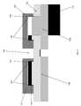
FIG. 3 , a back-gated FinFET/Tri-gate structure 300 fabricated on an SOI wafer is illustrated, wherein thestructure 300 comprises thesilicon substrate layer 212, anoxide layer 214, thefins 220, fabricated from the upper silicon layer of the SOI wafer, thefin isolation dielectrics 240 formed from the SOI buried insulator, and thegate electrode 260. Thestructure 300 also includes thegate isolation dielectrics 230 and thegate dielectrics 250. However, unlike thestructure 200, thefins 220 of thestructure 300 do not have thegate isolation dielectrics 230 and thegate dielectrics 250 on inner sidewalls thereof. Rather, as illustrated inFIG. 3 , thefins 220 haveback-gate dielectrics 360 on inner sidewalls thereof, wherein the inner sidewalls of thefins 220 are between thefins 220. Bottom surfaces of theback-gate dielectrics 360 contact thesilicon layer 212 and top portions of theback-gate dielectrics 360 contact thegate dielectrics 250. Theback-gate dielectrics 360 also contact thefin isolation dielectrics 240. - Further, the
structure 300 includes aback-gate electrode 370 between theback-gate dielectrics 360. More specifically, sidewalls of theback-gate electrode 370 contact theback-gate dielectrics 360; and, a top surface of theback-gate electrode 370 is above top surfaces of thefins 220. A bottom surface of theback-gate electrode 370 contacts thesilicon layer 212, wherein thestructure 300 does not include the buriedinsulator 240 or theoxide layer 214 between the inner sidewalls of thefins 220. - Additionally, an inter-gate-
electrode dielectric 380 is on the top surface and upper sidewalls of theback-gate electrode 370. The inter-gate-electrode dielectric 380 contacts theback-gate dielectrics 360 and thegate dielectrics 250. Furthermore, a heavily dopedregion 390 is included in theSOI 210. Specifically, the heavily dopedregion 390 is in an upper portion of thesilicon layer 212 and beneath theoxide layer 214, thefins 220, and theback-gate electrode 370. - Referring to
FIG. 4 , a back-gated FinFET/Tri-gate structure 400 havingfins 420 on a bulk substrate is illustrated. Thestructure 400 has primarily the same components as thestructure 300; however, thestructure 400 does not include thefin isolation dielectrics 240. By design, the thickness of the fin taken together with the doping concentration in the fins results in a fin which is fully depleted of mobile carriers (holes and electrons) and hence the channels222 in the fins are electrically isolated from theback-gate electrode 370. - The embodiments herein further provide a process of forming the
structure 100. Many of the details of forming fins, isolation regions, channel regions, dielectrics, gate electrodes, etc., are well-known and are not discussed herein in detail so as to focus the reader on the salient portions of the invention. Instead, reference is made to U.S. Patent Publications 20060043616 to Anderson et al. for the description of such details and the same are fully incorporated herein by reference. The following processes are only examples and the invention is not limited to the times, temperatures, materials, concentrations set forth below and instead can be formed using any similar processing. - The process begins with a bulk starting wafer with a silicon germanium (SiGe) layer having approximately 20-40% germanium. The SiGe layer is buried below a top pure silicon (Si) region. Heavily doped
regions 130 are formed by high-energy ion implantation. The energy is chosen so that the range of the ions implanted falls insideregion 130. A second high-energy implantation can additionally be used to dope theisolation regions 224, employing a somewhat lower energy than that used todope region 130. - Next, a silicon dioxide/silicon nitride (SiO2/Si3N4) cap layer is formed, wherein the cap layer is patterned to form a fin pattern. The silicon is etched using the cap layer as a mask to form the
fins 120, wherein the etch is stopped in the SiGe layer. The cap layer is subsequently stripped from the tops of thefins 120. Following this, a 600-degree Celsius oxidation process is performed on exposed regions of SiGe; and, thin oxide is grown in the pure Si regions. Thegate dielectrics fins 120; and, gate electrode material is formed and planarized. Finally, thegate electrodes 160 are patterned and etched; and, source and drain regions of exposedfins 120 are doped. - In the embodiment shown in
FIG. 2 , the starting wafer comprises a Silicon On Insulator (SOI) wafer. The buried insulator of the SOI wafer is used to form thefin isolation dielectric 240, and the top silicon of the SOI wafer is used to form thefins 220, in subsequent steps. Optionally, heavily dopedregions 210 are formed by high-energy ion implantation. The energy is chosen so that the range of the ions implanted falls insideregion 210. A second high-energy implantation can additionally be used to dope theisolation regions 224, employing a somewhat lower energy than that used to dope the lower, dopedregions 224. - Next, a silicon dioxide/silicon nitride (SiO2/Si3N4) cap layer is formed, wherein the cap layer is patterned to form a fin pattern. The silicon is etched using the cap layer as a mask to form the
fins 220, wherein the etch proceeds beyond the buriedoxide 240 and stops at a depth below the buried insulator that is typically between one and three times the fin thickness.Insulation region 214 is formed by a silicon ion implant into the exposed SOI wafer regions followed by an oxidation. The cap layer is subsequently stripped from the tops of thefins 120. Thegate dielectric 250 and thefin isolation dielectric 240 are then formed on surfaces of thefins 220, and lower, dopedregions 224, respectively; gate electrode material is formed and planarized. Finally, thegate electrodes 260 are patterned and etched; and, source and drain regions of exposedfins 220 are doped. - The embodiment of
FIG. 3 can be fabricated along the same lines as outlined forFIG. 2 , with the following deviations. After formation of thesilicon dioxide insulator 214, a mask is formed with an opening to allow the etch of thesilicon dioxide insulator 214 between the twofins 220.Dielectric 360 is formed on the exposed sides of the fins and the exposed surface of thesubstrate 212 betweenfins 220. A direction etch is used to remove the dielectric from thesubstrate 212. Theback-gate electrode 370 is formed by either in-situ-doped selective silicon growth or by non-selective deposition and etch-back/planarization. Next the mask is removed and thegate dielectric 250, dielectric230, and inter-gate dielectric380 are formed by oxidation and/or deposition processes. Gate electrode material is deposited, planarized, and patterned to formgate electrode 260. - A process of forming the
structure 400 is also provided. Many of the details of forming back-gate regions, well regions, fins, dielectrics, gate electrodes, etc., are well-known and are not discussed herein in detail so as to focus the reader on the salient portions of the invention. Instead, reference is made to U.S. Patent Publications 20050245009 to Bryant et al. for the description of such details and the same are fully incorporated herein by reference. - The process begins with a bulk starting wafer with a silicon germanium (SiGe) layer having approximately 20-40% germanium. The SiGe layer is buried below a top pure silicon (Si) region. Next, a silicon dioxide/silicon nitride (SiO2/Si3N4) cap layer is formed, wherein trenches are etched down to the SiGe layer (signal layer for the etch stop). The
back-gate dielectrics 360 are formed on surfaces and a thin layer of back-gate material is deposited. An anisotropic etch is then performed to form spacers on the trench sidewalls. Following this, exposedback-gate dielectrics 360 at the bottom of the trench are removed and the trenches are filled with back-gate electrode material. The back-gate material is planarized, wherein the polysilicon top of the back-gate material is subsequently oxidized (reacted). Next, the back-gate material is etched back until tops of the SiO2/Si3N4cap layer are exposed. The process then selectively etches the cap layer, wherein some loss of the reacted material on top of the back-gate may occur. Further, spacers (SiO2, Si3N4, or composite) are formed on exposed edges of the back-gate material. The silicon is anisotropically etched to form thefins 220 surrounding the back-gate region. Following this, the spacers over thefins 220 are removed and thegate dielectrics 250 are formed on exposed surfaces of the fins220 (including tops of the fins220). Front gate electrode material is also formed and planarized. The process then patterns and etches front and back gate electrodes and dopes source and drain regions of exposedfins 220. Processes for forming structures on SOI (e.g., thestructures 200 and300) are similar to the processes for forming structures on the bulk substrate (e.g., thestructures 100 and400). - Referring now to
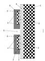
FIG. 5 , a top view of a rad-hard CMOS structure 500 is illustrated, wherein at least one nFET510 and at least one pFET520 are on anisolation region 530. More specifically, thenFET 510 includes agate 512, asource region 514, and adrain region 516. Similarly, thepFET 520 includes agate 522, asource region 524, and adrain region 526. AnSTI region 530 is between thenFET 510 and thepFET 520. FIG. 6 illustrates a cross-sectional view of theCMOS structure 500 on anSOI 610, wherein thenFET 510 and thepFET 520 includemesas 620 and630, respectively. Lower portions of themesas 620 and630 include a heavily p-dopedregion 622 and a heavily n-dopedregion 632, respectively. Themesas 620 and630 also havesidewall dielectrics sidewall dielectrics mesas 620 and630, respectively, and on at least a portion of lower sidewalls of themesas 620 and630, respectively. Thus, thesidewall dielectrics region 622 and the heavily n-dopedregion 632, respectively. As illustrated inFIG. 6 , thesidewall dielectrics region 622 and the heavily n-dopedregion 632, respectively. In other words, thesidewall dielectrics regions mesas 620,630 (upper channel regions).- The
mesas 620 and630 also havegate dielectrics gates sidewall dielectrics gate dielectrics gates region 622 and the heavily n-dopedregion 632, respectively. As illustrated inFIG. 6 , thegates region 622 and the heavily n-dopedregion 632, respectively. In other words, thegates regions mesas 620,630 (upper channel regions). TheSTI region 530 is between thegates - Referring now to
FIG. 7 a cross-sectional view of theCMOS structure 500 on abulk substrate 710 is illustrated. Unlike the structure inFIG. 6 , the heavily dopedregions isolation region 530 and into upper portions of thesubstrate 710. InFIG. 6 , theisolation region 530 separates the heavily dopedregions substrate 710. As shown inFIG. 7 , the heavily dopedregions regions substrate 710, and wherein upper portions of the heavily dopedregions mesas 620 and630. - A process for forming the CMOS structure500 (either on the
SOI 610 or the bulk substrate710) is also provided. TheSTI regions 530 are formed, followed by formation of the heavily dopedregions regions STI regions 530. Many of the details of forming STI regions, doped regions, mesas, dielectrics, gates, source/drain regions, etc., are well-known and are not discussed herein in detail so as to focus the reader on the salient portions of the invention. Instead, reference is made to U.S. Patent Publications 20060084212 to Anderson et al. for the description of such details and the same are fully incorporated herein by reference. - Next, the trench isolation is recessed (etched back) until at least some of the sidewalls of the heavily doped
regions mesas 620 and630 and thegate dielectrics gates sidewall dielectrics source regions drain regions nFET 510 and thepFET 520 via masking. Following this, the process performs annealing and silicide formation. Additional dielectrics are then deposited, etched, and vias are filled. Finally, interconnects are formed. - Accordingly, the embodiments of the invention provide a structure and method for a rad-hard FinFET. More specifically, a semiconductor structure is provided having at least one active area comprising a channel region on an isolation region. The active area may comprise a fin or a mesa, according to the embodiment employed. A doped substrate region (also referred to herein as the “heavily doped region”) is also provided below the active area, wherein the doped substrate region has a first polarity which may be opposite a second polarity of the channel region or the same polarity of the channel region. The isolation region contacts the doped substrate region.
- The structure further includes a gate electrode covering the channel region and at least a portion of the isolation region. Thus, as described above, the gate electrode is adjacent to the isolation region. The gate electrode comprises a lower portion below the channel region of the fin, wherein the lower portion of the gate electrode comprises a height that is at least one-half of a thickness of the fin. As described above, the structure could include an isolation oxide on portions of the top surface of the substrate that are not covered by the gate isolation dielectric. Thus, sidewalls of the isolation oxide contact sidewalls of the gate electrode.
- The structure further includes a gate dielectric on a top surface of the channel region, at least one sidewall of the channel region, and a portion of at least one sidewall of the isolation region. A gate isolation dielectric is also provided below the gate dielectric, wherein the gate isolation dielectric covers a portion of at least one sidewall of the isolation region. As described above, a boundary between the gate dielectric and the gate isolation dielectric is below a boundary between the channel region and the isolation region (with respect to the substrate).
- Additionally, a fin isolation dielectric is between the channel region and the isolation region. As described above, the gate isolation dielectrics and the fin isolation dielectrics can comprise the same, continuous, unbroken insulator layer. The gate electrode is on (covers) at least a portion of the fin isolation dielectric. As described above, the fin isolation dielectrics traverse the width of the fins; and as such, the fin isolation dielectrics are adjacent first sidewalls of the fins, continue through the body of the fins, and are adjacent second sidewalls of the fins, wherein the first sidewalls are opposite the second sidewalls. The structure can also include a back-gate electrode between a first fin and a second fin, wherein the back-gate electrode contacts the doped substrate region. As described above, sidewalls of the back-gate electrode contact back-gate dielectrics; and, a top surface of the back-gate electrode is above top surfaces of the fins.
- Another semiconductor structure is also provided having at least one fin comprising a lower doped region (also referred to herein as the “heavily p-doped region”, the “heavily n-doped region”, or the “heavily doped regions”) and an upper channel region, wherein the lower doped region is adjacent to at least one shallow isolation trench region. As described above,
FIG. 5 illustrates a top view of a rad-hard CMOS structure, wherein at least one nFET and at least one pFET are on an isolation region, and wherein an STI region is between the nFET and the pFET. A dielectric (also referred to herein as the “sidewall dielectric”) is also provided on at least one sidewall of the fin, wherein lower portions of the dielectric are on (cover) at least a portion of the lower doped region. As described above, the sidewall dielectrics overlap a border between the heavily doped regions and the remaining upper portions of the fins. - The structure further includes a gate electrode (also referred to herein as the “gates”) on the fin and the dielectric, wherein lower portions of the gate electrode are on (cover) the lower portions of the dielectric and the upper channel region. As described above, the gates are adjacent (proximate, cover, etc.) at least a portion of the heavily p-doped region and the heavily n-doped region. Moreover, the gates overlap a border between the heavily doped regions and the remaining upper portions of the fins. The gate electrode contacts at least one shallow isolation trench region.
- The embodiments of the invention also include a method of forming a semiconductor structure comprising forming a doped substrate region, wherein the doped substrate region comprises a first polarity. The method then forms at least one fin over the doped substrate region, such that the fin comprises a channel region having a second polarity which can be the same or opposite said first polarity on an isolation region, and such that the isolation region contacts the doped substrate region.
- Following this, a gate electrode is formed covering the channel region and at least a portion of the isolation region. Thus, as described above, the gate electrode is adjacent to the isolation region. The forming of the gate electrode comprises forming the gate electrode such that the gate electrode comprises a lower portion below the channel region of the fin (i.e., the portions of the
gate electrode 160 that are below thechannel region 122 of the fin120), and such that the lower portion of the gate electrode comprises a height that is at least one-half of a thickness of the fin. As described above, the structure could include an isolation oxide on portions of the top surface of the substrate that are not covered by the gate isolation dielectric. Thus, sidewalls of the isolation oxide contact sidewalls of the gate electrode. - Prior to the forming of the gate electrode, a gate dielectric is formed on a top surface of the channel region, on at least one sidewall of the channel region, and on a portion of at least one sidewall of the isolation region. Also prior to the forming of the gate electrode and during the forming of the gate dielectric, a gate isolation dielectric is formed such that the gate isolation dielectric is below the gate dielectric, and such that the gate isolation dielectric is on a portion of at least one sidewall of the isolation region. As described above, a boundary between the gate dielectric and the gate isolation dielectric is below a boundary between the channel region and the isolation region (with respect to the substrate).
- Furthermore, the method forms a fin isolation dielectric between the channel region and the isolation region. As described above, the gate isolation dielectrics and the fin isolation dielectrics can comprise the same, continuous, unbroken insulator layer. Thus, the forming of the gate electrode forms the gate electrode such that it covers at least a portion of the fin isolation dielectric. As described above, the fin isolation dielectrics traverse the width of the fins; and as such, the fin isolation dielectrics are adjacent first sidewalls of the fins, continue through the body of the fins, and are adjacent second sidewalls of the fins, wherein the first sidewalls are opposite the second sidewalls.
- Additionally, prior to the forming of the gate electrode, a back-gate electrode is formed between a first fin and a second fin, such that the back-gate electrode contacts the doped substrate region. As described above, sidewalls of the back-gate electrode contact back-gate dielectrics; and, a top surface of the back-gate electrode is above top surfaces of the fins.
- Another method of forming a semiconductor structure forms at least one fin comprising a lower doped region and an upper channel region. This includes forming the lower doped region such that the lower doped region is adjacent to at least one shallow isolation trench region. As described above,
FIG. 5 illustrates a top view of a rad-hard CMOS structure, wherein at least one nFET and at least one pFET are on an isolation region, and wherein an STI region is between the nFET and the pFET. - Following this, a dielectric is formed on at least one sidewall of the fin, such that lower portions of the dielectric cover at least a portion of the lower doped region. As described above, the sidewall dielectrics overlap a border between the heavily doped regions and the remaining upper portions of the fins. The method also forms a gate electrode on the fin and the dielectric, such that lower portions of the gate electrode cover the lower portions of the dielectric and the upper channel region. As described above, the gates are adjacent (proximate, cover, etc.) at least a portion of the heavily p-doped region and the heavily n-doped region. Moreover, the gates overlap a border between the heavily doped regions and the remaining upper portions of the fins. This involves forming the gate electrode such that the gate electrode contacts the shallow isolation trench region.
FIG. 8 is a flow diagram illustrating a method of forming a rad-hard FinFET. The method begins initem 810 by forming a doped substrate region, wherein the doped substrate region comprises a first polarity. The method, initem 820, then forms at least one fin over the doped substrate region, such that the fin comprises a channel region having a second polarity of the same, or opposite said first polarity on an isolation region, and such that the isolation region contacts the doped substrate region.- Prior to the forming of a gate electrode, in
item 830, a gate dielectric is formed on a top surface of the channel region, on at least one sidewall of the channel region, and on a portion of at least one sidewall of the isolation region. Also prior to the forming of the gate electrode and during the forming of the gate dielectric, initem 832, a gate isolation dielectric is formed such that the gate isolation dielectric is below the gate dielectric, and such that the gate isolation dielectric is on a portion of at least one sidewall of the isolation region. As described above, a boundary between the gate dielectric and the gate isolation dielectric is below a boundary between the channel region and the isolation region (with respect to the substrate). - In
item 840, the method forms a fin isolation dielectric between the channel region and the isolation region. As described above, the fin isolation dielectrics traverse the width of the fins; and as such, the fin isolation dielectrics are adjacent first sidewalls of the fins, continue through the body of the fins, and are adjacent second sidewalls of the fins, wherein the first sidewalls are opposite the second sidewalls. - Additionally, prior to the forming of the gate electrode, in
item 850, a back-gate electrode is formed between a first fin and a second fin, such that the back-gate electrode contacts the doped substrate region. As described above, sidewalls of the back-gate electrode contact back-gate dielectrics; and, a top surface of the back-gate electrode is above top surfaces of the fins. - Following this, in
item 860, a gate electrode is formed covering the channel region and at least a portion of the isolation region. Thus, as described above, the gate electrode is adjacent to the isolation region. This includes, initem 862, forming the gate electrode such that the gate electrode comprises a lower portion below the channel region of the fin, and such that the lower portion of the gate electrode comprises a height that is at least one-half of a thickness of the fin. As described above, the structure could include an isolation oxide on portions of the top surface of the substrate that are not covered by the gate isolation dielectric. Thus, sidewalls of the isolation oxide contact sidewalls of the gate electrode. Furthermore, initem 864, the forming of the gate electrode forms the gate electrode such that it covers at least a portion of the fin isolation dielectric. FIG. 9 is a flow diagram illustrating another method of forming a rad-hard FinFET. The method begins initem 910 by forming at least one fin comprising a lower doped region and an upper channel region. This includes, initem 912, forming the lower doped region such that the lower doped region is adjacent to at least one shallow isolation trench region. As described above,FIG. 5 illustrates a top view of a rad-hard CMOS structure, wherein at least one nFET and at least one pFET are on an isolation region, and wherein an STI region is between the nFET and the pFET.- Following this, in
item 920, a dielectric is formed on at least one sidewall of the fin, such that lower portions of the dielectric cover at least a portion of the lower doped region. As described above, the sidewall dielectrics overlap a border between the heavily doped regions and the remaining upper portions of the fins. The method, initem 930, also forms a gate electrode on the fin and the dielectric, such that lower portions of the gate electrode cover the lower portions of the dielectric and the upper channel region. As described above, the gates are adjacent (proximate, cover, etc.) at least a portion of the heavily p-doped region and the heavily n-doped region. Moreover, the gates overlap a border between the heavily doped regions and the remaining upper portions of the fins. This involves, initem 932, forming the gate electrode such that the gate electrode contacts the shallow isolation trench region. - Accordingly, features are introduced to FinFET technology to suppress degradation caused by exposure to various forms of ionizing radiation. In particular, regions that can accumulate charge and affect the channel potential are minimized by design. Furthermore, three elements which result in suppression of radiation-induced degradation are provided. First, a highly doped lower portion of the silicon sidewall adjacent to the STI is provided. Second, a sidewall dielectric region which overlaps at least a portion of the highly doped lower portion of the silicon sidewall is shown. Next, a continuation of the gate electrode from the top of the STI region downward sufficiently to overlap at least a portion of the sidewall dielectric region and at least a portion of the highly doped lower portion of the silicon sidewall is provided. This structure, applicable to both nFETs and pFETs, eliminates any thick oxide regions adjacent to lightly doped channel regions, hence augmenting resistance to radiation-induced degradation.
- Accordingly, features are introduced to FinFET technology to suppress degradation caused by exposure to various forms of ionizing radiation. In particular, regions that can accumulate charge and affect the channel potential are minimized by design. Furthermore, three elements which result in suppression of radiation-induced degradation are provided. First, a highly doped lower portion of the silicon sidewall adjacent to the STI is provided. Second, a sidewall dielectric region which overlaps at least a portion of the highly doped lower portion of the silicon sidewall is shown. Next, a continuation of the gate electrode from the top of the STI region downward sufficiently to overlap at least a portion of the sidewall dielectric region and at least a portion of the highly doped lower portion of the silicon sidewall is provided. This structure, applicable to both nFET and pFET, eliminates any thick oxide regions adjacent to lightly doped channel regions, hence augmenting resistance to radiation-induced degradation.
- The foregoing description of the specific embodiments will so fully reveal the general nature of the invention that others can, by applying current knowledge, readily modify and/or adapt for various applications such specific embodiments without departing from the generic concept, and, therefore, such adaptations and modifications should and are intended to be comprehended within the meaning and range of equivalents of the disclosed embodiments. It is to be understood that the phraseology or terminology employed herein is for the purpose of description and not of limitation. Therefore, while the embodiments of the invention have been described in terms of preferred embodiments, those skilled in the art will recognize that the embodiments of the invention can be practiced with modification within the spirit and scope of the appended claims.
Claims (20)
Priority Applications (1)
| Application Number | Priority Date | Filing Date | Title |
|---|---|---|---|
| US11/679,869US8735990B2 (en) | 2007-02-28 | 2007-02-28 | Radiation hardened FinFET |
Applications Claiming Priority (1)
| Application Number | Priority Date | Filing Date | Title |
|---|---|---|---|
| US11/679,869US8735990B2 (en) | 2007-02-28 | 2007-02-28 | Radiation hardened FinFET |
Publications (2)
| Publication Number | Publication Date |
|---|---|
| US20080203491A1true US20080203491A1 (en) | 2008-08-28 |
| US8735990B2 US8735990B2 (en) | 2014-05-27 |
Family
ID=39714905
Family Applications (1)
| Application Number | Title | Priority Date | Filing Date |
|---|---|---|---|
| US11/679,869Active2030-12-13US8735990B2 (en) | 2007-02-28 | 2007-02-28 | Radiation hardened FinFET |
Country Status (1)
| Country | Link |
|---|---|
| US (1) | US8735990B2 (en) |
Cited By (25)
| Publication number | Priority date | Publication date | Assignee | Title |
|---|---|---|---|---|
| US20100176438A1 (en)* | 2009-01-15 | 2010-07-15 | Macronix International Co., Ltd. | Depletion-mode charge-trapping flash device |
| US20110045648A1 (en)* | 2009-08-20 | 2011-02-24 | Globalfoundries Inc. | Methods for fabricating bulk finfet devices having deep trench isolation |
| CN102214676A (en)* | 2010-04-09 | 2011-10-12 | 中国科学院微电子研究所 | Semiconductor structure comprising fin and manufacturing method thereof |
| WO2012013037A1 (en)* | 2010-07-30 | 2012-02-02 | 中国科学院微电子研究所 | Semiconductor structure and manufacturing method thereof |
| CN103219384A (en)* | 2013-04-03 | 2013-07-24 | 北京大学 | Anti-single particle radiation multi-grid device and preparation method thereof |
| CN103426755A (en)* | 2012-05-14 | 2013-12-04 | 中芯国际集成电路制造(上海)有限公司 | Semiconductor component and forming method thereof |
| US8609480B2 (en) | 2011-12-21 | 2013-12-17 | Globalfoundries Inc. | Methods of forming isolation structures on FinFET semiconductor devices |
| US8803247B2 (en)* | 2011-12-15 | 2014-08-12 | United Microelectronics Corporation | Fin-type field effect transistor |
| CN103985750A (en)* | 2013-02-08 | 2014-08-13 | 中国科学院微电子研究所 | Semiconductor device and method for manufacturing the same |
| CN103985753A (en)* | 2013-02-08 | 2014-08-13 | 中国科学院微电子研究所 | Semiconductor device and method for manufacturing the same |
| CN103985754A (en)* | 2013-02-08 | 2014-08-13 | 中国科学院微电子研究所 | Semiconductor device and method for manufacturing the same |
| CN103985755A (en)* | 2013-02-08 | 2014-08-13 | 中国科学院微电子研究所 | Semiconductor arrangement and method for the production thereof |
| CN103985752A (en)* | 2013-02-08 | 2014-08-13 | 中国科学院微电子研究所 | Semiconductor arrangement and method for the production thereof |
| US20150001593A1 (en)* | 2013-06-28 | 2015-01-01 | Taiwan Semiconductor Manufacturing Co., Ltd. | Method for Forming Multi-Gate Device with Dual Channel |
| US8946064B2 (en) | 2011-06-16 | 2015-02-03 | International Business Machines Corporation | Transistor with buried silicon germanium for improved proximity control and optimized recess shape |
| WO2015027561A1 (en)* | 2013-08-30 | 2015-03-05 | 中国科学院微电子研究所 | Semiconductor device and method of manufacturing same |
| WO2015089454A1 (en)* | 2013-12-12 | 2015-06-18 | Texas Instruments Incorporated | Design and integration of finfet device |
| US20150311123A1 (en)* | 2012-11-09 | 2015-10-29 | Institute of Microelectronics, Chinese Academy of Sciences | Semiconductor device and method for manufacturing the same |
| US20150357350A1 (en)* | 2013-02-08 | 2015-12-10 | Institute of Microelectronics, Chinese Academy of Sciences | Semiconductor arrangements and methods for manufacturing the same |
| US20160111322A1 (en)* | 2013-11-18 | 2016-04-21 | Globalfoundries Inc. | Finfet semiconductor device having local buried oxide |
| CN106158859A (en)* | 2015-04-09 | 2016-11-23 | 中国科学院微电子研究所 | Semiconductor device and manufacturing method thereof |
| US20180138268A1 (en)* | 2016-11-14 | 2018-05-17 | Tokyo Electron Limited | Method of preventing bulk silicon charge transfer for nanowire and nanoslab processing |
| US20180247939A1 (en)* | 2015-09-25 | 2018-08-30 | Intel Corporation | Techniques for controlling transistor sub-fin leakage |
| EP3565006A1 (en)* | 2018-04-04 | 2019-11-06 | Korea Advanced Institute Of Science And Technology | Radiation-tolerant unit mosfet hardened against single event effect and total ionization dose effect |
| US20240014293A1 (en)* | 2022-07-11 | 2024-01-11 | Taiwan Semiconductor Manufacturing Company, Ltd. | Replacement structures |
Families Citing this family (3)
| Publication number | Priority date | Publication date | Assignee | Title |
|---|---|---|---|---|
| US9496181B2 (en) | 2014-12-23 | 2016-11-15 | Qualcomm Incorporated | Sub-fin device isolation |
| KR102323943B1 (en) | 2015-10-21 | 2021-11-08 | 삼성전자주식회사 | Method of manufacturing semiconductor device |
| US9515171B1 (en) | 2015-10-22 | 2016-12-06 | International Business Machines Corporation | Radiation tolerant device structure |
Citations (42)
| Publication number | Priority date | Publication date | Assignee | Title |
|---|---|---|---|---|
| US4683637A (en)* | 1986-02-07 | 1987-08-04 | Motorola, Inc. | Forming depthwise isolation by selective oxygen/nitrogen deep implant and reaction annealing |
| US5001526A (en)* | 1987-11-10 | 1991-03-19 | Fujitsu Limited | Dram cell formed on an insulating layer having a buried semiconductor pillar structure and a manufacturing method thereof |
| US5541130A (en)* | 1995-06-07 | 1996-07-30 | International Business Machines Corporation | Process for making and programming a flash memory array |
| US5641983A (en)* | 1992-07-31 | 1997-06-24 | Seiko Epson Corporation | Semiconductor device having a gate electrode having a low dopant concentration |
| US5796143A (en)* | 1996-10-30 | 1998-08-18 | Advanced Micro Devices, Inc. | Trench transistor in combination with trench array |
| US6448112B2 (en)* | 2000-02-24 | 2002-09-10 | Samsung Electronics Co., Ltd. | Cell array region of a NOR-type mask ROM device and fabricating method therefor |
| US6518112B2 (en)* | 1998-01-05 | 2003-02-11 | International Business Machines Corporation | High performance, low power vertical integrated CMOS devices |
| US6525403B2 (en)* | 2000-09-28 | 2003-02-25 | Kabushiki Kaisha Toshiba | Semiconductor device having MIS field effect transistors or three-dimensional structure |
| US6600200B1 (en)* | 1999-08-25 | 2003-07-29 | Infineon Technologies Ag | MOS transistor, method for fabricating a MOS transistor and method for fabricating two complementary MOS transistors |
| US20030161192A1 (en)* | 2000-09-12 | 2003-08-28 | Toshio Kobayashi | Nonvolatile semiconductor memory device and methods for operating and producing the same |
| US6664601B1 (en)* | 2000-06-22 | 2003-12-16 | Progressant Technologies, Inc. | Method of orperating a dual mode FET & logic circuit having negative differential resistance mode |
| US20040185626A1 (en)* | 2003-03-17 | 2004-09-23 | Yang Jeong-Hwan | Semiconductor device with different lattice properties |
| US6822281B2 (en)* | 2002-03-22 | 2004-11-23 | Infineon Technologies Ag | Trench cell for a DRAM cell array |
| US20040232471A1 (en)* | 2001-09-20 | 2004-11-25 | Shoji Shukuri | Semiconductor integrated circuit device and its manufacturing method |
| US20050035415A1 (en)* | 2003-08-13 | 2005-02-17 | Yee-Chia Yeo | Multiple-gate transistors formed on bulk substrates |
| US20050035391A1 (en)* | 2003-08-14 | 2005-02-17 | Lee Deok Hyung | Multi-structured Si-fin and method of manufacture |
| US6902969B2 (en)* | 2003-07-31 | 2005-06-07 | Freescale Semiconductor, Inc. | Process for forming dual metal gate structures |
| US20050167750A1 (en)* | 2004-01-30 | 2005-08-04 | Fu-Liang Yang | Methods and structures for planar and multiple-gate transistors formed on SOI |
| US20050173768A1 (en)* | 2004-02-10 | 2005-08-11 | Samsung Electronics Co., Ltd. | Fin fet structure |
| US20050218434A1 (en)* | 2004-04-06 | 2005-10-06 | Hyeoung-Won Seo | Transistor having asymmetric channel region, semiconductor device including the same, and method of fabricating semiconductor device including the same |
| US20050224800A1 (en)* | 2004-03-31 | 2005-10-13 | Nick Lindert | Bulk non-planar transistor having strained enhanced mobility and methods of fabrication |
| US20050227424A1 (en)* | 2004-04-09 | 2005-10-13 | Chang-Woo Oh | Semiconductor devices having a field effect transistor and methods of fabricating the same |
| US20050266628A1 (en)* | 2003-12-09 | 2005-12-01 | Daniel Wang | Substrate isolation in integrated circuits |
| US20050285153A1 (en)* | 2004-06-29 | 2005-12-29 | Rolf Weis | Transistor, memory cell array and method of manufacturing a transistor |
| US20060056228A1 (en)* | 2004-09-10 | 2006-03-16 | Till Schloesser | Transistor, memory cell array and method of manufacturing a transistor |
| US7019342B2 (en)* | 2003-07-03 | 2006-03-28 | American Semiconductor, Inc. | Double-gated transistor circuit |
| US20060110884A1 (en)* | 2004-09-10 | 2006-05-25 | Peng-Fei Wang | Method of manufacturing a transistor and a method of forming a memory device |
| US20060231907A1 (en)* | 2005-04-14 | 2006-10-19 | Samsung Electronics Co., Ltd. | Semiconductor device with FinFET and method of fabricating the same |
| US7166895B2 (en)* | 2004-05-19 | 2007-01-23 | Kabushiki Kaisha Toshiba | Semiconductor device including insulating film having a convex portion |
| US20070102763A1 (en)* | 2003-09-24 | 2007-05-10 | Yee-Chia Yeo | Multiple-gate transistors formed on bulk substrates |
| US20070134878A1 (en)* | 2005-12-09 | 2007-06-14 | Intel Corporation | Non-planar microelectronic device having isolation element to mitigate fringe effects and method to fabricate same |
| US20070194373A1 (en)* | 2006-02-22 | 2007-08-23 | Anderson Brent A | Cmos structure and method including multiple crystallographic planes |
| US20070249174A1 (en)* | 2006-04-21 | 2007-10-25 | International Business Machines Corporation | Patterning sub-lithographic features with variable widths |
| US7297600B2 (en)* | 2004-06-04 | 2007-11-20 | Samsung Electronics Co., Ltd. | Methods of forming fin field effect transistors using oxidation barrier layers |
| US20080006852A1 (en)* | 2005-09-19 | 2008-01-10 | Jochen Beintner | DENSE CHEVRON finFET AND METHOD OF MANUFACTURING SAME |
| US20080149984A1 (en)* | 2006-12-22 | 2008-06-26 | Chang Peter L D | Floating body memory cell having gates favoring different conductivity type regions |
| US20080157225A1 (en)* | 2006-12-29 | 2008-07-03 | Suman Datta | SRAM and logic transistors with variable height multi-gate transistor architecture |
| US7432160B2 (en)* | 2006-02-09 | 2008-10-07 | Samsung Electronics Co., Ltd. | Semiconductor devices including transistors having three dimensional channels and methods of fabricating the same |
| US20080303095A1 (en)* | 2007-06-07 | 2008-12-11 | Weize Xiong | Varying mugfet width to adjust device characteristics |
| US20090032859A1 (en)* | 2007-07-30 | 2009-02-05 | International Business Machines Corporation | Finfet flash memory device with an extended floating back gate |
| US20100038679A1 (en)* | 2008-08-14 | 2010-02-18 | International Business Machines Corporation | Finfet with longitudinal stress in a channel |
| US20100109057A1 (en)* | 2008-10-31 | 2010-05-06 | Samsung Electronics Co., Ltd. | Fin field effect transistor and method of fabricating the same |
- 2007
- 2007-02-28USUS11/679,869patent/US8735990B2/enactiveActive
Patent Citations (43)
| Publication number | Priority date | Publication date | Assignee | Title |
|---|---|---|---|---|
| US4683637A (en)* | 1986-02-07 | 1987-08-04 | Motorola, Inc. | Forming depthwise isolation by selective oxygen/nitrogen deep implant and reaction annealing |
| US5001526A (en)* | 1987-11-10 | 1991-03-19 | Fujitsu Limited | Dram cell formed on an insulating layer having a buried semiconductor pillar structure and a manufacturing method thereof |
| US5641983A (en)* | 1992-07-31 | 1997-06-24 | Seiko Epson Corporation | Semiconductor device having a gate electrode having a low dopant concentration |
| US5541130A (en)* | 1995-06-07 | 1996-07-30 | International Business Machines Corporation | Process for making and programming a flash memory array |
| US5796143A (en)* | 1996-10-30 | 1998-08-18 | Advanced Micro Devices, Inc. | Trench transistor in combination with trench array |
| US6518112B2 (en)* | 1998-01-05 | 2003-02-11 | International Business Machines Corporation | High performance, low power vertical integrated CMOS devices |
| US6600200B1 (en)* | 1999-08-25 | 2003-07-29 | Infineon Technologies Ag | MOS transistor, method for fabricating a MOS transistor and method for fabricating two complementary MOS transistors |
| US6448112B2 (en)* | 2000-02-24 | 2002-09-10 | Samsung Electronics Co., Ltd. | Cell array region of a NOR-type mask ROM device and fabricating method therefor |
| US6664601B1 (en)* | 2000-06-22 | 2003-12-16 | Progressant Technologies, Inc. | Method of orperating a dual mode FET & logic circuit having negative differential resistance mode |
| US20030161192A1 (en)* | 2000-09-12 | 2003-08-28 | Toshio Kobayashi | Nonvolatile semiconductor memory device and methods for operating and producing the same |
| US6525403B2 (en)* | 2000-09-28 | 2003-02-25 | Kabushiki Kaisha Toshiba | Semiconductor device having MIS field effect transistors or three-dimensional structure |
| US20040232471A1 (en)* | 2001-09-20 | 2004-11-25 | Shoji Shukuri | Semiconductor integrated circuit device and its manufacturing method |
| US6822281B2 (en)* | 2002-03-22 | 2004-11-23 | Infineon Technologies Ag | Trench cell for a DRAM cell array |
| US20040185626A1 (en)* | 2003-03-17 | 2004-09-23 | Yang Jeong-Hwan | Semiconductor device with different lattice properties |
| US7019342B2 (en)* | 2003-07-03 | 2006-03-28 | American Semiconductor, Inc. | Double-gated transistor circuit |
| US6902969B2 (en)* | 2003-07-31 | 2005-06-07 | Freescale Semiconductor, Inc. | Process for forming dual metal gate structures |
| US20050035415A1 (en)* | 2003-08-13 | 2005-02-17 | Yee-Chia Yeo | Multiple-gate transistors formed on bulk substrates |
| US20050035391A1 (en)* | 2003-08-14 | 2005-02-17 | Lee Deok Hyung | Multi-structured Si-fin and method of manufacture |
| US20070102763A1 (en)* | 2003-09-24 | 2007-05-10 | Yee-Chia Yeo | Multiple-gate transistors formed on bulk substrates |
| US20050266628A1 (en)* | 2003-12-09 | 2005-12-01 | Daniel Wang | Substrate isolation in integrated circuits |
| US20050167750A1 (en)* | 2004-01-30 | 2005-08-04 | Fu-Liang Yang | Methods and structures for planar and multiple-gate transistors formed on SOI |
| US7180134B2 (en)* | 2004-01-30 | 2007-02-20 | Taiwan Semiconductor Manufacturing Company, Ltd. | Methods and structures for planar and multiple-gate transistors formed on SOI |
| US20050173768A1 (en)* | 2004-02-10 | 2005-08-11 | Samsung Electronics Co., Ltd. | Fin fet structure |
| US20050224800A1 (en)* | 2004-03-31 | 2005-10-13 | Nick Lindert | Bulk non-planar transistor having strained enhanced mobility and methods of fabrication |
| US20050218434A1 (en)* | 2004-04-06 | 2005-10-06 | Hyeoung-Won Seo | Transistor having asymmetric channel region, semiconductor device including the same, and method of fabricating semiconductor device including the same |
| US20050227424A1 (en)* | 2004-04-09 | 2005-10-13 | Chang-Woo Oh | Semiconductor devices having a field effect transistor and methods of fabricating the same |
| US7166895B2 (en)* | 2004-05-19 | 2007-01-23 | Kabushiki Kaisha Toshiba | Semiconductor device including insulating film having a convex portion |
| US7297600B2 (en)* | 2004-06-04 | 2007-11-20 | Samsung Electronics Co., Ltd. | Methods of forming fin field effect transistors using oxidation barrier layers |
| US20050285153A1 (en)* | 2004-06-29 | 2005-12-29 | Rolf Weis | Transistor, memory cell array and method of manufacturing a transistor |
| US20060056228A1 (en)* | 2004-09-10 | 2006-03-16 | Till Schloesser | Transistor, memory cell array and method of manufacturing a transistor |
| US20060110884A1 (en)* | 2004-09-10 | 2006-05-25 | Peng-Fei Wang | Method of manufacturing a transistor and a method of forming a memory device |
| US20060231907A1 (en)* | 2005-04-14 | 2006-10-19 | Samsung Electronics Co., Ltd. | Semiconductor device with FinFET and method of fabricating the same |
| US20080006852A1 (en)* | 2005-09-19 | 2008-01-10 | Jochen Beintner | DENSE CHEVRON finFET AND METHOD OF MANUFACTURING SAME |
| US20070134878A1 (en)* | 2005-12-09 | 2007-06-14 | Intel Corporation | Non-planar microelectronic device having isolation element to mitigate fringe effects and method to fabricate same |
| US7432160B2 (en)* | 2006-02-09 | 2008-10-07 | Samsung Electronics Co., Ltd. | Semiconductor devices including transistors having three dimensional channels and methods of fabricating the same |
| US20070194373A1 (en)* | 2006-02-22 | 2007-08-23 | Anderson Brent A | Cmos structure and method including multiple crystallographic planes |
| US20070249174A1 (en)* | 2006-04-21 | 2007-10-25 | International Business Machines Corporation | Patterning sub-lithographic features with variable widths |
| US20080149984A1 (en)* | 2006-12-22 | 2008-06-26 | Chang Peter L D | Floating body memory cell having gates favoring different conductivity type regions |
| US20080157225A1 (en)* | 2006-12-29 | 2008-07-03 | Suman Datta | SRAM and logic transistors with variable height multi-gate transistor architecture |
| US20080303095A1 (en)* | 2007-06-07 | 2008-12-11 | Weize Xiong | Varying mugfet width to adjust device characteristics |
| US20090032859A1 (en)* | 2007-07-30 | 2009-02-05 | International Business Machines Corporation | Finfet flash memory device with an extended floating back gate |
| US20100038679A1 (en)* | 2008-08-14 | 2010-02-18 | International Business Machines Corporation | Finfet with longitudinal stress in a channel |
| US20100109057A1 (en)* | 2008-10-31 | 2010-05-06 | Samsung Electronics Co., Ltd. | Fin field effect transistor and method of fabricating the same |
Cited By (47)
| Publication number | Priority date | Publication date | Assignee | Title |
|---|---|---|---|---|
| US20100176438A1 (en)* | 2009-01-15 | 2010-07-15 | Macronix International Co., Ltd. | Depletion-mode charge-trapping flash device |
| TWI415249B (en)* | 2009-01-15 | 2013-11-11 | Macronix Int Co Ltd | Depletion mode charge trapping flash device |
| US8860124B2 (en)* | 2009-01-15 | 2014-10-14 | Macronix International Co., Ltd. | Depletion-mode charge-trapping flash device |
| US20110045648A1 (en)* | 2009-08-20 | 2011-02-24 | Globalfoundries Inc. | Methods for fabricating bulk finfet devices having deep trench isolation |
| US8039326B2 (en)* | 2009-08-20 | 2011-10-18 | Globalfoundries Inc. | Methods for fabricating bulk FinFET devices having deep trench isolation |
| CN102214676A (en)* | 2010-04-09 | 2011-10-12 | 中国科学院微电子研究所 | Semiconductor structure comprising fin and manufacturing method thereof |
| WO2012013037A1 (en)* | 2010-07-30 | 2012-02-02 | 中国科学院微电子研究所 | Semiconductor structure and manufacturing method thereof |
| CN102347350A (en)* | 2010-07-30 | 2012-02-08 | 中国科学院微电子研究所 | Semiconductor structure and manufacturing method thereof |
| US20120187418A1 (en)* | 2010-07-30 | 2012-07-26 | Haizhou Yin | Semiconductor structure and method for manufacturing the same |
| US8946064B2 (en) | 2011-06-16 | 2015-02-03 | International Business Machines Corporation | Transistor with buried silicon germanium for improved proximity control and optimized recess shape |
| US8803247B2 (en)* | 2011-12-15 | 2014-08-12 | United Microelectronics Corporation | Fin-type field effect transistor |
| US8692316B2 (en) | 2011-12-21 | 2014-04-08 | Globalfoundries Inc. | Isolation structures for FinFET semiconductor devices |
| US8609480B2 (en) | 2011-12-21 | 2013-12-17 | Globalfoundries Inc. | Methods of forming isolation structures on FinFET semiconductor devices |
| CN103426755A (en)* | 2012-05-14 | 2013-12-04 | 中芯国际集成电路制造(上海)有限公司 | Semiconductor component and forming method thereof |
| US20150311123A1 (en)* | 2012-11-09 | 2015-10-29 | Institute of Microelectronics, Chinese Academy of Sciences | Semiconductor device and method for manufacturing the same |
| US9748141B2 (en)* | 2012-11-09 | 2017-08-29 | Institute of Microelectronics, Chinese Academy of Sciences | Semiconductor device and method for manufacturing the same |
| WO2014121543A1 (en)* | 2013-02-08 | 2014-08-14 | 中国科学院微电子研究所 | Semiconductor device and manufacturing method thereof |
| US9461068B2 (en)* | 2013-02-08 | 2016-10-04 | Institute of Microelectronics, Chinese Academy of Sciences | Semiconductor arrangements and methods for manufacturing the same |
| WO2014121545A1 (en)* | 2013-02-08 | 2014-08-14 | 中国科学院微电子研究所 | Semiconductor device and manufacturing method thereof |
| CN103985754A (en)* | 2013-02-08 | 2014-08-13 | 中国科学院微电子研究所 | Semiconductor device and method for manufacturing the same |
| CN103985753A (en)* | 2013-02-08 | 2014-08-13 | 中国科学院微电子研究所 | Semiconductor device and method for manufacturing the same |
| US20150357350A1 (en)* | 2013-02-08 | 2015-12-10 | Institute of Microelectronics, Chinese Academy of Sciences | Semiconductor arrangements and methods for manufacturing the same |
| CN103985752A (en)* | 2013-02-08 | 2014-08-13 | 中国科学院微电子研究所 | Semiconductor arrangement and method for the production thereof |
| CN103985750A (en)* | 2013-02-08 | 2014-08-13 | 中国科学院微电子研究所 | Semiconductor device and method for manufacturing the same |
| CN103985755A (en)* | 2013-02-08 | 2014-08-13 | 中国科学院微电子研究所 | Semiconductor arrangement and method for the production thereof |
| US20150084127A1 (en)* | 2013-02-08 | 2015-03-26 | Huilong Zhu | Semiconductor device and method for manufacturing the same |
| US10134862B2 (en)* | 2013-02-08 | 2018-11-20 | Institute of Microelectronics, Chinese Academy of Sciences | Semiconductor device containing fin and back gate and method for manufacturing the same |
| CN103219384A (en)* | 2013-04-03 | 2013-07-24 | 北京大学 | Anti-single particle radiation multi-grid device and preparation method thereof |
| US9508852B2 (en) | 2013-04-03 | 2016-11-29 | Peking University | Radiation-hardened-by-design (RHBD) multi-gate device |
| US9000536B2 (en)* | 2013-06-28 | 2015-04-07 | Taiwan Semiconductor Manufacturing Co., Ltd. | Fin field effect transistor having a highly doped region |
| US20150001593A1 (en)* | 2013-06-28 | 2015-01-01 | Taiwan Semiconductor Manufacturing Co., Ltd. | Method for Forming Multi-Gate Device with Dual Channel |
| WO2015027561A1 (en)* | 2013-08-30 | 2015-03-05 | 中国科学院微电子研究所 | Semiconductor device and method of manufacturing same |
| US20160218218A1 (en)* | 2013-08-30 | 2016-07-28 | Institute of Microelectronics, Chinese Academy of Sciences | Semiconductor devices and methods for manufacturing the same |
| US9859434B2 (en)* | 2013-08-30 | 2018-01-02 | Institute Of Microelectronics, Chinese Acadamy Of Sciences | Semiconductor devices and methods for manufacturing the same |
| CN104425601A (en)* | 2013-08-30 | 2015-03-18 | 中国科学院微电子研究所 | Semiconductor device and method for manufacturing the same |
| US20160111322A1 (en)* | 2013-11-18 | 2016-04-21 | Globalfoundries Inc. | Finfet semiconductor device having local buried oxide |
| WO2015089454A1 (en)* | 2013-12-12 | 2015-06-18 | Texas Instruments Incorporated | Design and integration of finfet device |
| CN106158859A (en)* | 2015-04-09 | 2016-11-23 | 中国科学院微电子研究所 | Semiconductor device and manufacturing method thereof |
| US20180247939A1 (en)* | 2015-09-25 | 2018-08-30 | Intel Corporation | Techniques for controlling transistor sub-fin leakage |
| US10879241B2 (en)* | 2015-09-25 | 2020-12-29 | Intel Corporation | Techniques for controlling transistor sub-fin leakage |
| US20180138268A1 (en)* | 2016-11-14 | 2018-05-17 | Tokyo Electron Limited | Method of preventing bulk silicon charge transfer for nanowire and nanoslab processing |
| CN109952654A (en)* | 2016-11-14 | 2019-06-28 | 东京毅力科创株式会社 | Methods for preventing bulk silicon charge transfer in nanowire and nanoplate processing |
| US10490630B2 (en)* | 2016-11-14 | 2019-11-26 | Tokyo Electron Limited | Method of preventing bulk silicon charge transfer for nanowire and nanoslab processing |
| TWI746696B (en)* | 2016-11-14 | 2021-11-21 | 日商東京威力科創股份有限公司 | Method of preventing bulk silicon charge transfer for nanowire and nanoslab processing |
| EP3565006A1 (en)* | 2018-04-04 | 2019-11-06 | Korea Advanced Institute Of Science And Technology | Radiation-tolerant unit mosfet hardened against single event effect and total ionization dose effect |
| USRE50525E1 (en) | 2018-04-04 | 2025-08-05 | Korea Advanced Institute Of Science And Technology | Radiation-tolerant unit MOSFET hardened against single event effect and total ionization dose effect |
| US20240014293A1 (en)* | 2022-07-11 | 2024-01-11 | Taiwan Semiconductor Manufacturing Company, Ltd. | Replacement structures |
Also Published As
| Publication number | Publication date |
|---|---|
| US8735990B2 (en) | 2014-05-27 |
Similar Documents
| Publication | Publication Date | Title |
|---|---|---|
| US8735990B2 (en) | Radiation hardened FinFET | |
| JP5695730B2 (en) | Thin BOX metal back gate type ultrathin SOI device | |
| US7384850B2 (en) | Methods of forming complementary metal oxide semiconductor (CMOS) transistors having three-dimensional channel regions therein | |
| US8815659B2 (en) | Methods of forming a FinFET semiconductor device by performing an epitaxial growth process | |
| US8115251B2 (en) | Recessed gate channel with low Vt corner | |
| US7374988B2 (en) | NFET and PFET devices and methods of fabricating same | |
| US9048267B2 (en) | Semiconductor device | |
| JP2006049897A (en) | Method of manufacturing ultra-thin body field effect transistor (FET) device and ultra-thin body FET device manufactured thereby (ultra-thin body ultra-steep retrograde well (SSRW) FET device) | |
| JP2013045901A (en) | Semiconductor device and method of manufacturing semiconductor device | |
| US9059235B2 (en) | Semiconductor device and method of manufacturing the same | |
| SG185185A1 (en) | Mos semiconductor device and methods for its fabrication | |
| JP2013175700A (en) | Semiconductor device and manufacturing method of the same | |
| US7723777B2 (en) | Semiconductor device and method for making same | |
| US7514747B2 (en) | Silicon-on-insulator semiconductor device | |
| JP2015095568A (en) | Semiconductor device | |
| US9917087B2 (en) | Integrated circuits with a partially-depleted region formed over a bulk silicon substrate and methods for fabricating the same | |
| JP6840199B2 (en) | Semiconductor device | |
| JPH1093096A (en) | Semiconductor device and manufacturing method thereof | |
| JP5055697B2 (en) | Insulated gate field effect transistor and method of operating the same | |
| CN100416839C (en) | Partially depleted SOI MOS device | |
| US20180076280A1 (en) | Shallow drain metal-oxide-semiconductor transistors | |
| JP2004146847A (en) | Semiconductor device and manufacturing method thereof |
Legal Events
| Date | Code | Title | Description |
|---|---|---|---|
| AS | Assignment | Owner name:INTERNATIONAL BUSINESS MACHINES CORPORATION, NEW Y Free format text:ASSIGNMENT OF ASSIGNORS INTEREST;ASSIGNORS:ANDERSON, BRENT A.;DENNARD, ROBERT H.;HAKEY, MARK C.;AND OTHERS;REEL/FRAME:018939/0245;SIGNING DATES FROM 20070208 TO 20070222 Owner name:INTERNATIONAL BUSINESS MACHINES CORPORATION,NEW YO Free format text:ASSIGNMENT OF ASSIGNORS INTEREST;ASSIGNORS:ANDERSON, BRENT A.;DENNARD, ROBERT H.;HAKEY, MARK C.;AND OTHERS;SIGNING DATES FROM 20070208 TO 20070222;REEL/FRAME:018939/0245 Owner name:INTERNATIONAL BUSINESS MACHINES CORPORATION, NEW Y Free format text:ASSIGNMENT OF ASSIGNORS INTEREST;ASSIGNORS:ANDERSON, BRENT A.;DENNARD, ROBERT H.;HAKEY, MARK C.;AND OTHERS;SIGNING DATES FROM 20070208 TO 20070222;REEL/FRAME:018939/0245 | |
| STCF | Information on status: patent grant | Free format text:PATENTED CASE | |
| AS | Assignment | Owner name:GLOBALFOUNDRIES U.S. 2 LLC, NEW YORK Free format text:ASSIGNMENT OF ASSIGNORS INTEREST;ASSIGNOR:INTERNATIONAL BUSINESS MACHINES CORPORATION;REEL/FRAME:036550/0001 Effective date:20150629 | |
| AS | Assignment | Owner name:GLOBALFOUNDRIES INC., CAYMAN ISLANDS Free format text:ASSIGNMENT OF ASSIGNORS INTEREST;ASSIGNORS:GLOBALFOUNDRIES U.S. 2 LLC;GLOBALFOUNDRIES U.S. INC.;REEL/FRAME:036779/0001 Effective date:20150910 | |
| MAFP | Maintenance fee payment | Free format text:PAYMENT OF MAINTENANCE FEE, 4TH YEAR, LARGE ENTITY (ORIGINAL EVENT CODE: M1551) Year of fee payment:4 | |
| AS | Assignment | Owner name:WILMINGTON TRUST, NATIONAL ASSOCIATION, DELAWARE Free format text:SECURITY AGREEMENT;ASSIGNOR:GLOBALFOUNDRIES INC.;REEL/FRAME:049490/0001 Effective date:20181127 | |
| AS | Assignment | Owner name:GLOBALFOUNDRIES U.S. INC., CALIFORNIA Free format text:ASSIGNMENT OF ASSIGNORS INTEREST;ASSIGNOR:GLOBALFOUNDRIES INC.;REEL/FRAME:054633/0001 Effective date:20201022 | |
| AS | Assignment | Owner name:GLOBALFOUNDRIES INC., CAYMAN ISLANDS Free format text:RELEASE BY SECURED PARTY;ASSIGNOR:WILMINGTON TRUST, NATIONAL ASSOCIATION;REEL/FRAME:054636/0001 Effective date:20201117 | |
| AS | Assignment | Owner name:GLOBALFOUNDRIES U.S. INC., NEW YORK Free format text:RELEASE BY SECURED PARTY;ASSIGNOR:WILMINGTON TRUST, NATIONAL ASSOCIATION;REEL/FRAME:056987/0001 Effective date:20201117 | |
| MAFP | Maintenance fee payment | Free format text:PAYMENT OF MAINTENANCE FEE, 8TH YEAR, LARGE ENTITY (ORIGINAL EVENT CODE: M1552); ENTITY STATUS OF PATENT OWNER: LARGE ENTITY Year of fee payment:8 |