US20080199982A1 - Fabrication Process for Package With Light Emitting Device On A Sub-Mount - Google Patents
Fabrication Process for Package With Light Emitting Device On A Sub-MountDownload PDFInfo
- Publication number
- US20080199982A1 US20080199982A1US11/675,179US67517907AUS2008199982A1US 20080199982 A1US20080199982 A1US 20080199982A1US 67517907 AUS67517907 AUS 67517907AUS 2008199982 A1US2008199982 A1US 2008199982A1
- Authority
- US
- United States
- Prior art keywords
- metallization
- deposited
- feed
- conductive pad
- interconnections
- Prior art date
- Legal status (The legal status is an assumption and is not a legal conclusion. Google has not performed a legal analysis and makes no representation as to the accuracy of the status listed.)
- Granted
Links
- 238000004519manufacturing processMethods0.000titleclaimsabstractdescription10
- 238000000034methodMethods0.000titleclaimsdescription53
- 238000001465metallisationMethods0.000claimsabstractdescription111
- 238000000151depositionMethods0.000claimsabstractdescription25
- 239000004065semiconductorSubstances0.000claimsabstractdescription15
- 239000000463materialSubstances0.000claimsabstractdescription13
- 229910052782aluminiumInorganic materials0.000claimsdescription13
- 239000010931goldSubstances0.000claimsdescription13
- XAGFODPZIPBFFR-UHFFFAOYSA-NaluminiumChemical compound[Al]XAGFODPZIPBFFR-UHFFFAOYSA-N0.000claimsdescription12
- PCHJSUWPFVWCPO-UHFFFAOYSA-NgoldChemical compound[Au]PCHJSUWPFVWCPO-UHFFFAOYSA-N0.000claimsdescription11
- 229910052737goldInorganic materials0.000claimsdescription11
- 229920002120photoresistant polymerPolymers0.000claimsdescription10
- 238000009713electroplatingMethods0.000claimsdescription5
- 238000005530etchingMethods0.000claimsdescription4
- 238000004070electrodepositionMethods0.000claimsdescription3
- 230000008020evaporationEffects0.000claimsdescription3
- 238000001704evaporationMethods0.000claimsdescription3
- 238000004544sputter depositionMethods0.000claimsdescription3
- 238000010923batch productionMethods0.000claimsdescription2
- 238000003618dip coatingMethods0.000claimsdescription2
- 238000004528spin coatingMethods0.000claimsdescription2
- 238000005507sprayingMethods0.000claimsdescription2
- ATJFFYVFTNAWJD-UHFFFAOYSA-NTinChemical compound[Sn]ATJFFYVFTNAWJD-UHFFFAOYSA-N0.000claims2
- 230000008878couplingEffects0.000claims1
- 238000010168coupling processMethods0.000claims1
- 238000005859coupling reactionMethods0.000claims1
- 230000008021depositionEffects0.000abstractdescription6
- 238000007747platingMethods0.000description7
- 229910000679solderInorganic materials0.000description6
- 239000010409thin filmSubstances0.000description5
- XUIMIQQOPSSXEZ-UHFFFAOYSA-NSiliconChemical compound[Si]XUIMIQQOPSSXEZ-UHFFFAOYSA-N0.000description4
- 229910052710siliconInorganic materials0.000description4
- 239000010703siliconSubstances0.000description4
- PXHVJJICTQNCMI-UHFFFAOYSA-NNickelChemical compound[Ni]PXHVJJICTQNCMI-UHFFFAOYSA-N0.000description3
- 239000010936titaniumSubstances0.000description3
- 230000015572biosynthetic processEffects0.000description2
- 239000004020conductorSubstances0.000description2
- JVPLOXQKFGYFMN-UHFFFAOYSA-Ngold tinChemical compound[Sn].[Au]JVPLOXQKFGYFMN-UHFFFAOYSA-N0.000description2
- 229910052719titaniumInorganic materials0.000description2
- RTAQQCXQSZGOHL-UHFFFAOYSA-NTitaniumChemical compound[Ti]RTAQQCXQSZGOHL-UHFFFAOYSA-N0.000description1
- 238000004026adhesive bondingMethods0.000description1
- 238000000637aluminium metallisationMethods0.000description1
- 239000011521glassSubstances0.000description1
- 229910052751metalInorganic materials0.000description1
- 239000002184metalSubstances0.000description1
- 229910052759nickelInorganic materials0.000description1
- 230000003287optical effectEffects0.000description1
- 238000002161passivationMethods0.000description1
- 229920001296polysiloxanePolymers0.000description1
- 238000005476solderingMethods0.000description1
- 238000010561standard procedureMethods0.000description1
Images


Classifications
- H—ELECTRICITY
- H10—SEMICONDUCTOR DEVICES; ELECTRIC SOLID-STATE DEVICES NOT OTHERWISE PROVIDED FOR
- H10H—INORGANIC LIGHT-EMITTING SEMICONDUCTOR DEVICES HAVING POTENTIAL BARRIERS
- H10H20/00—Individual inorganic light-emitting semiconductor devices having potential barriers, e.g. light-emitting diodes [LED]
- H10H20/80—Constructional details
- H10H20/85—Packages
- H10H20/8506—Containers
- H—ELECTRICITY
- H10—SEMICONDUCTOR DEVICES; ELECTRIC SOLID-STATE DEVICES NOT OTHERWISE PROVIDED FOR
- H10H—INORGANIC LIGHT-EMITTING SEMICONDUCTOR DEVICES HAVING POTENTIAL BARRIERS
- H10H20/00—Individual inorganic light-emitting semiconductor devices having potential barriers, e.g. light-emitting diodes [LED]
- H10H20/80—Constructional details
- H10H20/85—Packages
- H10H20/855—Optical field-shaping means, e.g. lenses
- H10H20/856—Reflecting means
- H—ELECTRICITY
- H01—ELECTRIC ELEMENTS
- H01L—SEMICONDUCTOR DEVICES NOT COVERED BY CLASS H10
- H01L2224/00—Indexing scheme for arrangements for connecting or disconnecting semiconductor or solid-state bodies and methods related thereto as covered by H01L24/00
- H01L2224/01—Means for bonding being attached to, or being formed on, the surface to be connected, e.g. chip-to-package, die-attach, "first-level" interconnects; Manufacturing methods related thereto
- H01L2224/42—Wire connectors; Manufacturing methods related thereto
- H01L2224/47—Structure, shape, material or disposition of the wire connectors after the connecting process
- H01L2224/48—Structure, shape, material or disposition of the wire connectors after the connecting process of an individual wire connector
- H01L2224/4805—Shape
- H01L2224/4809—Loop shape
- H01L2224/48091—Arched
- H—ELECTRICITY
- H01—ELECTRIC ELEMENTS
- H01L—SEMICONDUCTOR DEVICES NOT COVERED BY CLASS H10
- H01L2224/00—Indexing scheme for arrangements for connecting or disconnecting semiconductor or solid-state bodies and methods related thereto as covered by H01L24/00
- H01L2224/01—Means for bonding being attached to, or being formed on, the surface to be connected, e.g. chip-to-package, die-attach, "first-level" interconnects; Manufacturing methods related thereto
- H01L2224/42—Wire connectors; Manufacturing methods related thereto
- H01L2224/47—Structure, shape, material or disposition of the wire connectors after the connecting process
- H01L2224/48—Structure, shape, material or disposition of the wire connectors after the connecting process of an individual wire connector
- H01L2224/481—Disposition
- H01L2224/48151—Connecting between a semiconductor or solid-state body and an item not being a semiconductor or solid-state body, e.g. chip-to-substrate, chip-to-passive
- H01L2224/48221—Connecting between a semiconductor or solid-state body and an item not being a semiconductor or solid-state body, e.g. chip-to-substrate, chip-to-passive the body and the item being stacked
- H01L2224/48225—Connecting between a semiconductor or solid-state body and an item not being a semiconductor or solid-state body, e.g. chip-to-substrate, chip-to-passive the body and the item being stacked the item being non-metallic, e.g. insulating substrate with or without metallisation
- H01L2224/48235—Connecting between a semiconductor or solid-state body and an item not being a semiconductor or solid-state body, e.g. chip-to-substrate, chip-to-passive the body and the item being stacked the item being non-metallic, e.g. insulating substrate with or without metallisation connecting the wire to a via metallisation of the item
- H—ELECTRICITY
- H01—ELECTRIC ELEMENTS
- H01L—SEMICONDUCTOR DEVICES NOT COVERED BY CLASS H10
- H01L2224/00—Indexing scheme for arrangements for connecting or disconnecting semiconductor or solid-state bodies and methods related thereto as covered by H01L24/00
- H01L2224/73—Means for bonding being of different types provided for in two or more of groups H01L2224/10, H01L2224/18, H01L2224/26, H01L2224/34, H01L2224/42, H01L2224/50, H01L2224/63, H01L2224/71
- H01L2224/732—Location after the connecting process
- H01L2224/73251—Location after the connecting process on different surfaces
- H01L2224/73265—Layer and wire connectors
- H—ELECTRICITY
- H01—ELECTRIC ELEMENTS
- H01L—SEMICONDUCTOR DEVICES NOT COVERED BY CLASS H10
- H01L2924/00—Indexing scheme for arrangements or methods for connecting or disconnecting semiconductor or solid-state bodies as covered by H01L24/00
- H01L2924/10—Details of semiconductor or other solid state devices to be connected
- H01L2924/102—Material of the semiconductor or solid state bodies
- H01L2924/1025—Semiconducting materials
- H01L2924/10251—Elemental semiconductors, i.e. Group IV
- H01L2924/10253—Silicon [Si]
- H—ELECTRICITY
- H01—ELECTRIC ELEMENTS
- H01L—SEMICONDUCTOR DEVICES NOT COVERED BY CLASS H10
- H01L2924/00—Indexing scheme for arrangements or methods for connecting or disconnecting semiconductor or solid-state bodies as covered by H01L24/00
- H01L2924/30—Technical effects
- H01L2924/301—Electrical effects
- H01L2924/3025—Electromagnetic shielding
- H—ELECTRICITY
- H10—SEMICONDUCTOR DEVICES; ELECTRIC SOLID-STATE DEVICES NOT OTHERWISE PROVIDED FOR
- H10H—INORGANIC LIGHT-EMITTING SEMICONDUCTOR DEVICES HAVING POTENTIAL BARRIERS
- H10H20/00—Individual inorganic light-emitting semiconductor devices having potential barriers, e.g. light-emitting diodes [LED]
- H10H20/80—Constructional details
- H10H20/85—Packages
- H10H20/857—Interconnections, e.g. lead-frames, bond wires or solder balls
Definitions
- This disclosurerelates to a fabrication process for a package with a light emitting device on a sub-mount.
- LEDsoften are housed in packages that include multiple components, which occupy an area much larger than the LED chip itself.
- a reflective materialsuch as metallization, sometimes is provided on the inner surface of the package.
- the LED chipis bonded to a thermally conductive pad.
- the metallization for the reflective mirroralso may serve as part of a thin-film stack for the conductive pad and for plated through-wafer interconnections. Such processes, however, tend to complicate the fabrication process and reduce the amount of the package surface that can be used to reflect light out of the package.
- a method of fabricating a package with a light emitting deviceincludes depositing a first metallization to form a conductive pad on which the light emitting device is to be mounted and to form one or more feed-through interconnections extending through a semiconductor material that supports the conductive pad. Subsequently, a second metallization is deposited to form a reflective surface for reflecting light, emitted by the light emitting device, through a lid of the package. Deposition of the second metallization is de-coupled from deposition of the first metallization, which, in some cases, can increase the area covered by the reflective metallization, thereby increasing the amount of light reflected out of the package.
- the first metallizationis deposited so as to form respective overhangs around the top of the conductive pad and each of the feed-through interconnections.
- the second metallizationis deposited over a surface of the semiconductor material such that the overhangs serve as shields to substantially prevent the second metallization from being deposited on areas directly below the overhangs. Such a technique allows the second metallization to form a reflective surface that is electrically disconnected from the conductive pad and the feed-through interconnections.
- Some implementationsinclude forming a cavity in a first side of a semiconductor wafer and forming one or more through-holes that extend from a bottom of the cavity to a second side of the wafer.
- the first metallizationis deposited to form the conductive pad for mounting the light emitting device and to form feed-through interconnections that extend through the one or more through-holes.
- the first metallizationis deposited so as to form overhangs around the top of the conductive pad and each of the feed-through interconnections.
- the second metallizationis deposited over the first side of the semiconductor wafer including over bottom and side surfaces of the cavity and over top surfaces of the conductive pad and the feed-through interconnections.
- the overhangsserve as shields to substantially prevent the second metallization from being deposited on areas directly below the overhangs.
- the second metallizationis removed selectively from top surfaces of the conductive pad and the feed-through interconnections, so that the remaining second metallization forms a reflective surface that is electrically disconnected from the conductive pad and the feed-through interconnections.
- the light emitting devicethen is mounted on the conductive pad.
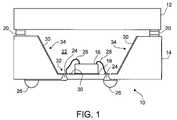
- FIG. 1is a cross-section of an example of a package that houses a light emitting device.
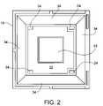
- FIG. 2is a top view of the base of the package.
- FIGS. 3 through 7illustrate fabrication steps for depositing the various metallization layers.
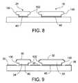
- FIG. 8is an enlarged view of overhangs at the top of feed-through and conductive pad metallization regions.
- FIG. 9illustrates how the overhangs shield areas adjacent the side edges of the feed-through and conductive pad metallization regions from being covered by subsequently deposited metallization.
- two structures 12 , 14are soldered together to provide a hermetically sealed package 10 that encapsulates a light emitting device, such as a LED 16 .
- a light emitting devicesuch as a LED 16 .
- Techniques other than solderingmay be used as well (e.g., but not limited to, anodic bonding and adhesive bonding).
- the upper structure 12serves as a lid and is transparent to the wavelength(s) that are emitted by the LED 16 .
- the LED chip 16is mounted on a conductive pad 18 on the lower structure 14 , which serves as a base.
- a solder seal ring 20is provided on the cavity-side surface of the base structure 14 for hermetically attaching the lid 12 to the base.
- FIG. 2is a top view of the base 14 with the LED chip 16 removed.
- the LED 16is mounted within a recessed cavity 22 formed in the base 14 , which also includes feed-through metallization 24 .
- Other circuitry as well as passive componentsmay be mounted in the recessed cavity 22 and encapsulated within the package.
- the feed-through metallization 24extends through one or more micro-vias (i.e., through-holes) in the lower section of the base 14 .
- the feed-through metallization 24extends along the outer surface of the base 14 and may be electrically connected to solder bumps 26 for printed circuit board assembly. Wire bonds 28 may provide the electrical connections from the LED chip 16 to the feed-through metallization 24 .
- the LED 16may be flip-chip connected directly to the feed-through metallization 24 .
- Metallization 30also is provided on inner surfaces of the base 14 , including the bottom 32 and sidewalls 34 , and serves as a mirror to reflect additional light, emitted by the LED 16 , through the lid 12 .
- the base 14can be formed, for example, from a silicon wafer into which the recessed cavity 22 and through-holes for the feed-through metallization 24 are etched using standard techniques. For example, a double-sided etching technique can be used.
- FIGS. 3 through 7illustrate fabrication steps for depositing the various metallization layers.
- a thin-film metallization stack 40is deposited over the surfaces of the wafer, including in the cavity and the through-holes.
- the thin-film stack 40includes layers of aluminum (Al), titanium (Ti), nickel (Ni) and gold (Au).
- Alaluminum
- Tititanium
- Ninickel
- Augold
- Other implementationsmay include fewer than all the foregoing materials.
- additional, or different, materialsmay be included for the thin-film stack in other implementations.
- a thin plating mould 42is provided over the surfaces of the silicon wafer other than the areas where the feed-through metallization 24 and conductive pad 18 are to be deposited.
- a photoresist maskcan be used as the plating mould 42 .
- FIGS. 3-7illustrate an example with respect to the feed-through metallization 24 , the same processes are used with respect to the pad metallization 18 .
- the photoresist maskcan be deposited by any of several techniques, including, for example, spin coating, dip coating, spray coating or electro-deposition.
- the metallization for the feed-through connections 24 and the pad 18is deposited using, for example, an electroplating process.
- the electroplated metallization 18 , 24is deposited so that there is an overhang around the top of each conductor line and/or pad.
- An enlarged example of such an overhang 100is illustrated in FIG. 8 .
- the overhang 100serves as a shield to prevent the mirror metallization 30 from being deposited too close to the side edges of the metallization for the feed-through connections 24 and the pad 18 .
- gold (Au) or gold-tinis used as the metallization for the feed-through connections 24 and the pad 18 .
- isotropic growth of the gold layerresults in formation of the overhang 100 .
- the thickness of the plating mould 42is about 7-8 microns ( ⁇ m), and the thickness of the gold metallization is about 10 ⁇ m.
- the thickness of the overhangsis about 2-3 ⁇ m.
- the overhangs 100extend about 2-3 ⁇ m beyond the lower portions of the metallization. In other implementations, those values may differ.
- the plating mould 42is removed, and the remaining thin-film stack 40 is patterned to form metal structures, such as a solder bond 44 and solder dam 46 on the backside of the silicon wafer.
- the solder bond 44includes all the layers of the film-stack 40 ; the solder dam 46 includes the Al and Ti layers.
- the mirror metallization (e.g., aluminum) 30is deposited on substantially all the exposed areas of the cavity-side of the base 14 .
- Evaporation or sputtering techniquescan be used to deposit the mirror metallization 30 , which should have a final thickness that is less than the thickness of the lower portion of the metallization for the feed-through connections 24 and the conductive pad 18 .
- the mirror metallization 30has a thickness of about one hundred nanometers (nm).
- the mirror metallizationis deposited on the top of the overhangs 100 as well as on exposed areas of the cavity-side of the base 14 .
- the overhangs 100 for the feed-through connections 24 and the conductive pad 18serve as shields and prevent the mirror metallization from being deposited too close to the edges of the feed-through connections 24 and the pad 18 .
- the process of depositing the mirror metallization 30is de-coupled from the process of depositing the metallization for the feed-through connections 24 and the conductive pad 18 . That can result in the mirror metallization 30 covering a large percentage of the interior surfaces of the base 14 , while preventing the mirror metallization from contacting the side edges of the feed-through connections 24 and the pad 18 .
- the aluminum mirror metallization 30is removed from the gold plating layers 24 , 18 (i.e., the aluminum is removed from the top of the feed-through connections 24 and the conductive pad 18 ). That can be achieved, for example, by selectively depositing a photoresist layer 48 (e.g., by an electro-deposition technique) on areas of the aluminum mirror metallization layer 30 other than on those areas where the aluminum mirror metallization layer is to be removed (i.e., other than on the feed-through connections 24 and the conductive pad 18 ). The exposed aluminum metallization on the tops of the gold (or gold-tin) feed-through connections 24 and the conductive pad 18 then can be removed by placing the silicon wafer in an aluminum etchant.
- a photoresist layer 48e.g., by an electro-deposition technique
- the electro-deposited photoresist layer 48is stripped, as shown in FIG. 7 .
- the resultis a semiconductor sub-mount for the LED chip with a significant portion of the inner surface covered by a reflective (mirror) metallization to enhance optical output.
- the mirror metallizationis electrically disconnected from the conductor lines (i.e., the feed-through connections 24 and the conductive pad 18 ) as a result of the overhangs 100 .
- the processcan be performed as a batch process at the wafer level.
- the LED chip 16is placed on the conductive pad 18 , and the wire-bonds 28 are attached.
- the cavity 22can be filled with a silicone gel, and the transparent lid 12 , which can include a plastic or glass lens, is attached to the base 14 .
Landscapes
- Led Device Packages (AREA)
Abstract
Description
- This disclosure relates to a fabrication process for a package with a light emitting device on a sub-mount.
- The design of packages that house a light emitting diode (LED) or other light emitting device is an important factor in optimizing the amount of light output from the package. LEDs often are housed in packages that include multiple components, which occupy an area much larger than the LED chip itself. To increase the amount of light emitted from the package, a reflective material, such as metallization, sometimes is provided on the inner surface of the package. To maximize the amount of light reflected out of the package, it is desirable to provide the reflective material over a significant part of the package interior.
- In some packages, the LED chip is bonded to a thermally conductive pad. The metallization for the reflective mirror also may serve as part of a thin-film stack for the conductive pad and for plated through-wafer interconnections. Such processes, however, tend to complicate the fabrication process and reduce the amount of the package surface that can be used to reflect light out of the package.
- In one aspect, a method of fabricating a package with a light emitting device, such as a LED, includes depositing a first metallization to form a conductive pad on which the light emitting device is to be mounted and to form one or more feed-through interconnections extending through a semiconductor material that supports the conductive pad. Subsequently, a second metallization is deposited to form a reflective surface for reflecting light, emitted by the light emitting device, through a lid of the package. Deposition of the second metallization is de-coupled from deposition of the first metallization, which, in some cases, can increase the area covered by the reflective metallization, thereby increasing the amount of light reflected out of the package.
- In some implementations, the first metallization is deposited so as to form respective overhangs around the top of the conductive pad and each of the feed-through interconnections. The second metallization is deposited over a surface of the semiconductor material such that the overhangs serve as shields to substantially prevent the second metallization from being deposited on areas directly below the overhangs. Such a technique allows the second metallization to form a reflective surface that is electrically disconnected from the conductive pad and the feed-through interconnections.
- Some implementations include forming a cavity in a first side of a semiconductor wafer and forming one or more through-holes that extend from a bottom of the cavity to a second side of the wafer. The first metallization is deposited to form the conductive pad for mounting the light emitting device and to form feed-through interconnections that extend through the one or more through-holes. The first metallization is deposited so as to form overhangs around the top of the conductive pad and each of the feed-through interconnections. The second metallization is deposited over the first side of the semiconductor wafer including over bottom and side surfaces of the cavity and over top surfaces of the conductive pad and the feed-through interconnections. The overhangs serve as shields to substantially prevent the second metallization from being deposited on areas directly below the overhangs. The second metallization is removed selectively from top surfaces of the conductive pad and the feed-through interconnections, so that the remaining second metallization forms a reflective surface that is electrically disconnected from the conductive pad and the feed-through interconnections. The light emitting device then is mounted on the conductive pad.
- The details of one or more embodiments of the invention are set forth in the accompanying drawings and the description below. Other features and advantages of the invention will be apparent from the detailed description, the accompanying drawings, and the claims.
FIG. 1 is a cross-section of an example of a package that houses a light emitting device.FIG. 2 is a top view of the base of the package.FIGS. 3 through 7 illustrate fabrication steps for depositing the various metallization layers.FIG. 8 is an enlarged view of overhangs at the top of feed-through and conductive pad metallization regions.FIG. 9 illustrates how the overhangs shield areas adjacent the side edges of the feed-through and conductive pad metallization regions from being covered by subsequently deposited metallization.- As illustrated in the example of
FIG. 1 , twostructures package 10 that encapsulates a light emitting device, such as aLED 16. Techniques other than soldering may be used as well (e.g., but not limited to, anodic bonding and adhesive bonding). Theupper structure 12 serves as a lid and is transparent to the wavelength(s) that are emitted by theLED 16. - In the illustrated example, the
LED chip 16 is mounted on aconductive pad 18 on thelower structure 14, which serves as a base. Asolder seal ring 20 is provided on the cavity-side surface of thebase structure 14 for hermetically attaching thelid 12 to the base. FIG. 2 is a top view of thebase 14 with theLED chip 16 removed.- As shown in
FIGS. 1 and 2 , theLED 16 is mounted within arecessed cavity 22 formed in thebase 14, which also includes feed-throughmetallization 24. Other circuitry as well as passive components may be mounted in therecessed cavity 22 and encapsulated within the package. The feed-throughmetallization 24 extends through one or more micro-vias (i.e., through-holes) in the lower section of thebase 14. As illustrated in the example ofFIG. 1 , the feed-throughmetallization 24 extends along the outer surface of thebase 14 and may be electrically connected tosolder bumps 26 for printed circuit board assembly.Wire bonds 28 may provide the electrical connections from theLED chip 16 to the feed-throughmetallization 24. Alternatively, theLED 16 may be flip-chip connected directly to the feed-throughmetallization 24.Metallization 30 also is provided on inner surfaces of thebase 14, including thebottom 32 andsidewalls 34, and serves as a mirror to reflect additional light, emitted by theLED 16, through thelid 12. - The
base 14 can be formed, for example, from a silicon wafer into which therecessed cavity 22 and through-holes for the feed-throughmetallization 24 are etched using standard techniques. For example, a double-sided etching technique can be used. - The metallization for the
pad 18 and feed-throughconnections 24, as well as themirror metallization 30, subsequently are deposited. As explained in greater detail below, deposition of themirror metallization 30 is de-coupled from deposition of the metallization for thepad 18 and feed-throughconnections 24. FIGS. 3 through 7 illustrate fabrication steps for depositing the various metallization layers. As shown inFIG. 3 , following etching of thecavity 22 and the through-holes for the feed-throughmetallization 24, and depositing or growing a passivation layer, a thin-film metallization stack 40 is deposited over the surfaces of the wafer, including in the cavity and the through-holes. In the illustrated example, the thin-film stack 40 includes layers of aluminum (Al), titanium (Ti), nickel (Ni) and gold (Au). Other implementations may include fewer than all the foregoing materials. Furthermore, additional, or different, materials may be included for the thin-film stack in other implementations.- Next, a
thin plating mould 42 is provided over the surfaces of the silicon wafer other than the areas where the feed-throughmetallization 24 andconductive pad 18 are to be deposited. A photoresist mask can be used as theplating mould 42. AlthoughFIGS. 3-7 illustrate an example with respect to the feed-throughmetallization 24, the same processes are used with respect to thepad metallization 18. The photoresist mask can be deposited by any of several techniques, including, for example, spin coating, dip coating, spray coating or electro-deposition. - After depositing the
plating mould 42, the metallization for the feed-throughconnections 24 and thepad 18 is deposited using, for example, an electroplating process. Theelectroplated metallization overhang 100 is illustrated inFIG. 8 . During subsequent fabrication processes, theoverhang 100 serves as a shield to prevent themirror metallization 30 from being deposited too close to the side edges of the metallization for the feed-throughconnections 24 and thepad 18. - In the illustrated example, gold (Au) or gold-tin is used as the metallization for the feed-through
connections 24 and thepad 18. Once the thickness of deposited gold exceeds the thickness of theplating mould 42, isotropic growth of the gold layer results in formation of theoverhang 100. In the illustrated example, the thickness of theplating mould 42 is about 7-8 microns (μm), and the thickness of the gold metallization is about 10 μm. The thickness of the overhangs is about 2-3 μm. Similarly, in the illustrated example, theoverhangs 100 extend about 2-3 μm beyond the lower portions of the metallization. In other implementations, those values may differ. - Next, as illustrated in
FIG. 4 , theplating mould 42 is removed, and the remaining thin-film stack 40 is patterned to form metal structures, such as asolder bond 44 andsolder dam 46 on the backside of the silicon wafer. In the illustrated example, thesolder bond 44 includes all the layers of the film-stack 40; thesolder dam 46 includes the Al and Ti layers. - Next, as shown in
FIG. 5 , the mirror metallization (e.g., aluminum)30 is deposited on substantially all the exposed areas of the cavity-side of thebase 14. Evaporation or sputtering techniques can be used to deposit themirror metallization 30, which should have a final thickness that is less than the thickness of the lower portion of the metallization for the feed-throughconnections 24 and theconductive pad 18. In the illustrated example, themirror metallization 30 has a thickness of about one hundred nanometers (nm). As illustrated inFIG. 5 , the mirror metallization is deposited on the top of theoverhangs 100 as well as on exposed areas of the cavity-side of thebase 14. As mentioned above, however, and as illustrated more clearly inFIG. 9 , theoverhangs 100 for the feed-throughconnections 24 and theconductive pad 18 serve as shields and prevent the mirror metallization from being deposited too close to the edges of the feed-throughconnections 24 and thepad 18. - As is clear from the foregoing description, the process of depositing the
mirror metallization 30 is de-coupled from the process of depositing the metallization for the feed-throughconnections 24 and theconductive pad 18. That can result in themirror metallization 30 covering a large percentage of the interior surfaces of thebase 14, while preventing the mirror metallization from contacting the side edges of the feed-throughconnections 24 and thepad 18. - Next, as shown in
FIG. 6 , thealuminum mirror metallization 30 is removed from the gold plating layers24,18 (i.e., the aluminum is removed from the top of the feed-throughconnections 24 and the conductive pad18). That can be achieved, for example, by selectively depositing a photoresist layer48 (e.g., by an electro-deposition technique) on areas of the aluminummirror metallization layer 30 other than on those areas where the aluminum mirror metallization layer is to be removed (i.e., other than on the feed-throughconnections 24 and the conductive pad18). The exposed aluminum metallization on the tops of the gold (or gold-tin) feed-throughconnections 24 and theconductive pad 18 then can be removed by placing the silicon wafer in an aluminum etchant. - After removing the aluminum from the feed-through
connections 24 and theconductive pad 18, the electro-depositedphotoresist layer 48 is stripped, as shown inFIG. 7 . The result is a semiconductor sub-mount for the LED chip with a significant portion of the inner surface covered by a reflective (mirror) metallization to enhance optical output. The mirror metallization is electrically disconnected from the conductor lines (i.e., the feed-throughconnections 24 and the conductive pad18) as a result of theoverhangs 100. - Although the foregoing description focuses on formation of the
base 14 for a single package, the process can be performed as a batch process at the wafer level. After the various metallization layers have been deposited, theLED chip 16 is placed on theconductive pad 18, and the wire-bonds 28 are attached. Thecavity 22 can be filled with a silicone gel, and thetransparent lid 12, which can include a plastic or glass lens, is attached to thebase 14. - Other implementations are within the scope of the claims.
Claims (29)
Priority Applications (3)
| Application Number | Priority Date | Filing Date | Title |
|---|---|---|---|
| US11/675,179US7732234B2 (en) | 2007-02-15 | 2007-02-15 | Fabrication process for package with light emitting device on a sub-mount |
| PCT/EP2008/051020WO2008098832A1 (en) | 2007-02-15 | 2008-01-29 | Fabrication process for package with light emitting device on a sub-mount |
| TW097105101ATWI523255B (en) | 2007-02-15 | 2008-02-14 | Method for manufacturing light-emitting device on substrate |
Applications Claiming Priority (1)
| Application Number | Priority Date | Filing Date | Title |
|---|---|---|---|
| US11/675,179US7732234B2 (en) | 2007-02-15 | 2007-02-15 | Fabrication process for package with light emitting device on a sub-mount |
Publications (2)
| Publication Number | Publication Date |
|---|---|
| US20080199982A1true US20080199982A1 (en) | 2008-08-21 |
| US7732234B2 US7732234B2 (en) | 2010-06-08 |
Family
ID=39358337
Family Applications (1)
| Application Number | Title | Priority Date | Filing Date |
|---|---|---|---|
| US11/675,179Expired - Fee RelatedUS7732234B2 (en) | 2007-02-15 | 2007-02-15 | Fabrication process for package with light emitting device on a sub-mount |
Country Status (3)
| Country | Link |
|---|---|
| US (1) | US7732234B2 (en) |
| TW (1) | TWI523255B (en) |
| WO (1) | WO2008098832A1 (en) |
Cited By (9)
| Publication number | Priority date | Publication date | Assignee | Title |
|---|---|---|---|---|
| US20100176507A1 (en)* | 2009-01-14 | 2010-07-15 | Hymite A/S | Semiconductor-based submount with electrically conductive feed-throughs |
| US20120104445A1 (en)* | 2010-11-03 | 2012-05-03 | Yang ming-kun | Chip package and method for forming the same |
| US20130043502A1 (en)* | 2010-05-31 | 2013-02-21 | Panasonic Corporation | Light emitting device and method for manufacturing the same |
| CN104009030A (en)* | 2013-02-20 | 2014-08-27 | 马克西姆综合产品公司 | Multichip wafer level package (WLP) optical device |
| US20170323872A1 (en)* | 2014-11-04 | 2017-11-09 | Osram Opto Semiconductors Gmbh | Optoelectronic component and method of producing same |
| US9859179B2 (en)* | 2013-09-27 | 2018-01-02 | Kyocera Corporation | Lid body, package, and electronic apparatus |
| WO2018235925A1 (en)* | 2017-06-22 | 2018-12-27 | Agc株式会社 | Window material, optical package |
| WO2019065633A1 (en)* | 2017-09-26 | 2019-04-04 | 京セラ株式会社 | Wiring board and light emitting device |
| JPWO2019163987A1 (en)* | 2018-02-26 | 2021-02-12 | 京セラ株式会社 | Electronic component mounting packages, electronic devices and electronic modules |
Families Citing this family (5)
| Publication number | Priority date | Publication date | Assignee | Title |
|---|---|---|---|---|
| TWI423467B (en)* | 2007-06-06 | 2014-01-11 | Epistar Corp | Semiconductor light emitting device |
| JP5640632B2 (en) | 2010-03-12 | 2014-12-17 | 旭硝子株式会社 | Light emitting device |
| TWI572922B (en)* | 2013-01-31 | 2017-03-01 | 鴻海精密工業股份有限公司 | Optical fiber connector |
| FR3003403B1 (en) | 2013-03-14 | 2016-11-04 | Commissariat Energie Atomique | METHOD FOR FORMING LIGHT EMITTING DIODES |
| JP2017046014A (en)* | 2016-12-01 | 2017-03-02 | 日亜化学工業株式会社 | Optical semiconductor device |
Citations (7)
| Publication number | Priority date | Publication date | Assignee | Title |
|---|---|---|---|---|
| US6531328B1 (en)* | 2001-10-11 | 2003-03-11 | Solidlite Corporation | Packaging of light-emitting diode |
| US20060001055A1 (en)* | 2004-02-23 | 2006-01-05 | Kazuhiko Ueno | Led and fabrication method of same |
| US20060054910A1 (en)* | 2004-09-14 | 2006-03-16 | Hideaki Takemori | Submount for light emitting diode and its manufacturing method |
| US7165896B2 (en)* | 2004-02-12 | 2007-01-23 | Hymite A/S | Light transmitting modules with optical power monitoring |
| US7247940B2 (en)* | 2003-02-28 | 2007-07-24 | Osram Opto Semiconductor Gmbh | Optoelectronic device with patterned-metallized package body, method for producing such a device and method for the patterned metallization of a plastic-containing body |
| US20080006837A1 (en)* | 2006-07-07 | 2008-01-10 | Lg Electronics Inc. And Lg Innotek Co., Ltd | Sub-mount for mounting light emitting device and light emitting device package |
| US7411225B2 (en)* | 2005-03-21 | 2008-08-12 | Lg Electronics Inc. | Light source apparatus |
Family Cites Families (3)
| Publication number | Priority date | Publication date | Assignee | Title |
|---|---|---|---|---|
| US6949771B2 (en) | 2001-04-25 | 2005-09-27 | Agilent Technologies, Inc. | Light source |
| DE602004027890D1 (en) | 2003-03-18 | 2010-08-12 | Sumitomo Electric Industries | HOUSING FOR LIGHT-EMITTING ELEMENT AND USE OF SEMI-FINISHED COMPONENT |
| JP2007027278A (en) | 2005-07-13 | 2007-02-01 | Shinko Electric Ind Co Ltd | Semiconductor device and manufacturing method of semiconductor device |
- 2007
- 2007-02-15USUS11/675,179patent/US7732234B2/ennot_activeExpired - Fee Related
- 2008
- 2008-01-29WOPCT/EP2008/051020patent/WO2008098832A1/enactiveApplication Filing
- 2008-02-14TWTW097105101Apatent/TWI523255B/ennot_activeIP Right Cessation
Patent Citations (7)
| Publication number | Priority date | Publication date | Assignee | Title |
|---|---|---|---|---|
| US6531328B1 (en)* | 2001-10-11 | 2003-03-11 | Solidlite Corporation | Packaging of light-emitting diode |
| US7247940B2 (en)* | 2003-02-28 | 2007-07-24 | Osram Opto Semiconductor Gmbh | Optoelectronic device with patterned-metallized package body, method for producing such a device and method for the patterned metallization of a plastic-containing body |
| US7165896B2 (en)* | 2004-02-12 | 2007-01-23 | Hymite A/S | Light transmitting modules with optical power monitoring |
| US20060001055A1 (en)* | 2004-02-23 | 2006-01-05 | Kazuhiko Ueno | Led and fabrication method of same |
| US20060054910A1 (en)* | 2004-09-14 | 2006-03-16 | Hideaki Takemori | Submount for light emitting diode and its manufacturing method |
| US7411225B2 (en)* | 2005-03-21 | 2008-08-12 | Lg Electronics Inc. | Light source apparatus |
| US20080006837A1 (en)* | 2006-07-07 | 2008-01-10 | Lg Electronics Inc. And Lg Innotek Co., Ltd | Sub-mount for mounting light emitting device and light emitting device package |
Cited By (15)
| Publication number | Priority date | Publication date | Assignee | Title |
|---|---|---|---|---|
| US20100176507A1 (en)* | 2009-01-14 | 2010-07-15 | Hymite A/S | Semiconductor-based submount with electrically conductive feed-throughs |
| US20130043502A1 (en)* | 2010-05-31 | 2013-02-21 | Panasonic Corporation | Light emitting device and method for manufacturing the same |
| US20120104445A1 (en)* | 2010-11-03 | 2012-05-03 | Yang ming-kun | Chip package and method for forming the same |
| TWI450345B (en)* | 2010-11-03 | 2014-08-21 | Xintec Inc | Chip package and method of forming same |
| CN104009030A (en)* | 2013-02-20 | 2014-08-27 | 马克西姆综合产品公司 | Multichip wafer level package (WLP) optical device |
| US9859179B2 (en)* | 2013-09-27 | 2018-01-02 | Kyocera Corporation | Lid body, package, and electronic apparatus |
| US20170323872A1 (en)* | 2014-11-04 | 2017-11-09 | Osram Opto Semiconductors Gmbh | Optoelectronic component and method of producing same |
| WO2018235925A1 (en)* | 2017-06-22 | 2018-12-27 | Agc株式会社 | Window material, optical package |
| JPWO2018235925A1 (en)* | 2017-06-22 | 2020-05-21 | Agc株式会社 | Window material, optical package |
| JP7205470B2 (en) | 2017-06-22 | 2023-01-17 | Agc株式会社 | Window materials, optical packages |
| WO2019065633A1 (en)* | 2017-09-26 | 2019-04-04 | 京セラ株式会社 | Wiring board and light emitting device |
| JPWO2019065633A1 (en)* | 2017-09-26 | 2020-11-19 | 京セラ株式会社 | Wiring board and light emitting device |
| JP7054704B2 (en) | 2017-09-26 | 2022-04-14 | 京セラ株式会社 | Wiring board and light emitting device |
| JPWO2019163987A1 (en)* | 2018-02-26 | 2021-02-12 | 京セラ株式会社 | Electronic component mounting packages, electronic devices and electronic modules |
| JP7142080B2 (en) | 2018-02-26 | 2022-09-26 | 京セラ株式会社 | Packages for mounting electronic components, electronic devices and electronic modules |
Also Published As
| Publication number | Publication date |
|---|---|
| TW200901511A (en) | 2009-01-01 |
| US7732234B2 (en) | 2010-06-08 |
| TWI523255B (en) | 2016-02-21 |
| WO2008098832A1 (en) | 2008-08-21 |
Similar Documents
| Publication | Publication Date | Title |
|---|---|---|
| US7732234B2 (en) | Fabrication process for package with light emitting device on a sub-mount | |
| US10446726B2 (en) | Wafer level packaging of electronic devices | |
| US7179670B2 (en) | Flip-chip light emitting diode device without sub-mount | |
| US8852969B2 (en) | Fabrication of compact opto-electronic component packages | |
| US6614103B1 (en) | Plastic packaging of LED arrays | |
| CN100514591C (en) | A method of manufacturing semiconductor packages and packages made | |
| US20100001305A1 (en) | Semiconductor devices and fabrication methods thereof | |
| US20100038668A1 (en) | Semiconductor device and method of manufacturing the same | |
| TWI593140B (en) | Structure and method for carrying light-emitting device | |
| US20110303936A1 (en) | Light emitting device package structure and fabricating method thereof | |
| US20100176507A1 (en) | Semiconductor-based submount with electrically conductive feed-throughs | |
| US11749777B2 (en) | Method for manufacturing light-emitting module | |
| KR20150119604A (en) | Wafer Level Chip Scale Light Emitting Diode Package | |
| WO2014142448A1 (en) | Wafer level chip scale light emitting diode package | |
| WO2013081328A1 (en) | Light emitting diode package and method of manufacturing light emitting diode package | |
| US20150099319A1 (en) | LED Package with Slanting Structure and Method of the Same | |
| US8729591B2 (en) | Opto-electronic device package with a semiconductor-based sub-mount having SMD metal contacts | |
| US9117941B2 (en) | LED package and method of the same | |
| US20150001570A1 (en) | LED Package and Method of the Same |
Legal Events
| Date | Code | Title | Description |
|---|---|---|---|
| AS | Assignment | Owner name:HYMITE A/S, DENMARK Free format text:ASSIGNMENT OF ASSIGNORS INTEREST;ASSIGNORS:GREISEN, CHRISTOFFER GRAAE;HESCHEL, MATTHIAS;SHIV, LIOR;AND OTHERS;REEL/FRAME:019238/0421;SIGNING DATES FROM 20070316 TO 20070319 Owner name:HYMITE A/S,DENMARK Free format text:ASSIGNMENT OF ASSIGNORS INTEREST;ASSIGNORS:GREISEN, CHRISTOFFER GRAAE;HESCHEL, MATTHIAS;SHIV, LIOR;AND OTHERS;SIGNING DATES FROM 20070316 TO 20070319;REEL/FRAME:019238/0421 | |
| FEPP | Fee payment procedure | Free format text:PAT HOLDER NO LONGER CLAIMS SMALL ENTITY STATUS, ENTITY STATUS SET TO UNDISCOUNTED (ORIGINAL EVENT CODE: STOL); ENTITY STATUS OF PATENT OWNER: LARGE ENTITY | |
| STCF | Information on status: patent grant | Free format text:PATENTED CASE | |
| AS | Assignment | Owner name:TAIWAN SEMICONDUCTOR MANUFACTURING COMPANY, LTD., Free format text:ASSIGNMENT OF ASSIGNORS INTEREST;ASSIGNOR:HYMITE A/S;REEL/FRAME:025403/0566 Effective date:20100809 | |
| FPAY | Fee payment | Year of fee payment:4 | |
| AS | Assignment | Owner name:CHIP STAR LTD., TAIWAN Free format text:ASSIGNMENT OF ASSIGNORS INTEREST;ASSIGNOR:TAIWAN SEMICONDUCTOR MANUFACTURING COMPANY, LTD.;REEL/FRAME:036543/0245 Effective date:20150624 | |
| AS | Assignment | Owner name:EPISTAR CORPORATION, TAIWAN Free format text:MERGER;ASSIGNOR:CHIP STAR LTD.;REEL/FRAME:038107/0949 Effective date:20150715 | |
| MAFP | Maintenance fee payment | Free format text:PAYMENT OF MAINTENANCE FEE, 8TH YEAR, LARGE ENTITY (ORIGINAL EVENT CODE: M1552) Year of fee payment:8 | |
| FEPP | Fee payment procedure | Free format text:MAINTENANCE FEE REMINDER MAILED (ORIGINAL EVENT CODE: REM.); ENTITY STATUS OF PATENT OWNER: LARGE ENTITY | |
| LAPS | Lapse for failure to pay maintenance fees | Free format text:PATENT EXPIRED FOR FAILURE TO PAY MAINTENANCE FEES (ORIGINAL EVENT CODE: EXP.); ENTITY STATUS OF PATENT OWNER: LARGE ENTITY | |
| STCH | Information on status: patent discontinuation | Free format text:PATENT EXPIRED DUE TO NONPAYMENT OF MAINTENANCE FEES UNDER 37 CFR 1.362 | |
| FP | Lapsed due to failure to pay maintenance fee | Effective date:20220608 |