US20080196666A1 - Shower head and cvd apparatus using the same - Google Patents
Shower head and cvd apparatus using the sameDownload PDFInfo
- Publication number
- US20080196666A1 US20080196666A1US11/826,336US82633607AUS2008196666A1US 20080196666 A1US20080196666 A1US 20080196666A1US 82633607 AUS82633607 AUS 82633607AUS 2008196666 A1US2008196666 A1US 2008196666A1
- Authority
- US
- United States
- Prior art keywords
- gas
- showerhead
- plate
- gas diffusion
- workpiece
- Prior art date
- Legal status (The legal status is an assumption and is not a legal conclusion. Google has not performed a legal analysis and makes no representation as to the accuracy of the status listed.)
- Abandoned
Links
- 238000009792diffusion processMethods0.000claimsabstractdescription130
- 239000002184metalSubstances0.000claimsabstractdescription32
- 238000000034methodMethods0.000claimsdescription26
- 239000011148porous materialSubstances0.000claimsdescription7
- 150000004767nitridesChemical class0.000claimsdescription5
- 230000000149penetrating effectEffects0.000claimsdescription4
- 238000005229chemical vapour depositionMethods0.000description26
- 238000004891communicationMethods0.000description8
- 229910052581Si3N4Inorganic materials0.000description7
- 239000000919ceramicSubstances0.000description7
- 239000000463materialSubstances0.000description7
- HQVNEWCFYHHQES-UHFFFAOYSA-Nsilicon nitrideChemical compoundN12[Si]34N5[Si]62N3[Si]51N64HQVNEWCFYHHQES-UHFFFAOYSA-N0.000description6
- BLRPTPMANUNPDV-UHFFFAOYSA-NSilaneChemical compound[SiH4]BLRPTPMANUNPDV-UHFFFAOYSA-N0.000description5
- 238000009413insulationMethods0.000description4
- 238000004519manufacturing processMethods0.000description4
- 239000012466permeateSubstances0.000description4
- 239000004020conductorSubstances0.000description3
- -1e.g.Substances0.000description3
- 230000035699permeabilityEffects0.000description3
- 238000005245sinteringMethods0.000description3
- 229910004205SiNXInorganic materials0.000description2
- 229910010293ceramic materialInorganic materials0.000description2
- 238000006243chemical reactionMethods0.000description2
- 238000005553drillingMethods0.000description2
- 238000000465mouldingMethods0.000description2
- 239000004065semiconductorSubstances0.000description2
- 238000000748compression mouldingMethods0.000description1
- 238000010494dissociation reactionMethods0.000description1
- 230000005593dissociationsEffects0.000description1
- 238000009826distributionMethods0.000description1
- 238000002474experimental methodMethods0.000description1
- 150000002500ionsChemical class0.000description1
- 230000002093peripheral effectEffects0.000description1
- 238000005268plasma chemical vapour depositionMethods0.000description1
- 230000000452restraining effectEffects0.000description1
- 238000007789sealingMethods0.000description1
- 238000005507sprayingMethods0.000description1
- 229910001220stainless steelInorganic materials0.000description1
- 239000010935stainless steelSubstances0.000description1
- 239000000126substanceSubstances0.000description1
- 230000008719thickeningEffects0.000description1
Images


Classifications
- C—CHEMISTRY; METALLURGY
- C23—COATING METALLIC MATERIAL; COATING MATERIAL WITH METALLIC MATERIAL; CHEMICAL SURFACE TREATMENT; DIFFUSION TREATMENT OF METALLIC MATERIAL; COATING BY VACUUM EVAPORATION, BY SPUTTERING, BY ION IMPLANTATION OR BY CHEMICAL VAPOUR DEPOSITION, IN GENERAL; INHIBITING CORROSION OF METALLIC MATERIAL OR INCRUSTATION IN GENERAL
- C23C—COATING METALLIC MATERIAL; COATING MATERIAL WITH METALLIC MATERIAL; SURFACE TREATMENT OF METALLIC MATERIAL BY DIFFUSION INTO THE SURFACE, BY CHEMICAL CONVERSION OR SUBSTITUTION; COATING BY VACUUM EVAPORATION, BY SPUTTERING, BY ION IMPLANTATION OR BY CHEMICAL VAPOUR DEPOSITION, IN GENERAL
- C23C16/00—Chemical coating by decomposition of gaseous compounds, without leaving reaction products of surface material in the coating, i.e. chemical vapour deposition [CVD] processes
- C23C16/44—Chemical coating by decomposition of gaseous compounds, without leaving reaction products of surface material in the coating, i.e. chemical vapour deposition [CVD] processes characterised by the method of coating
- C23C16/455—Chemical coating by decomposition of gaseous compounds, without leaving reaction products of surface material in the coating, i.e. chemical vapour deposition [CVD] processes characterised by the method of coating characterised by the method used for introducing gases into reaction chamber or for modifying gas flows in reaction chamber
- C23C16/45563—Gas nozzles
- C23C16/45565—Shower nozzles
- C—CHEMISTRY; METALLURGY
- C23—COATING METALLIC MATERIAL; COATING MATERIAL WITH METALLIC MATERIAL; CHEMICAL SURFACE TREATMENT; DIFFUSION TREATMENT OF METALLIC MATERIAL; COATING BY VACUUM EVAPORATION, BY SPUTTERING, BY ION IMPLANTATION OR BY CHEMICAL VAPOUR DEPOSITION, IN GENERAL; INHIBITING CORROSION OF METALLIC MATERIAL OR INCRUSTATION IN GENERAL
- C23C—COATING METALLIC MATERIAL; COATING MATERIAL WITH METALLIC MATERIAL; SURFACE TREATMENT OF METALLIC MATERIAL BY DIFFUSION INTO THE SURFACE, BY CHEMICAL CONVERSION OR SUBSTITUTION; COATING BY VACUUM EVAPORATION, BY SPUTTERING, BY ION IMPLANTATION OR BY CHEMICAL VAPOUR DEPOSITION, IN GENERAL
- C23C16/00—Chemical coating by decomposition of gaseous compounds, without leaving reaction products of surface material in the coating, i.e. chemical vapour deposition [CVD] processes
- C23C16/44—Chemical coating by decomposition of gaseous compounds, without leaving reaction products of surface material in the coating, i.e. chemical vapour deposition [CVD] processes characterised by the method of coating
- C23C16/50—Chemical coating by decomposition of gaseous compounds, without leaving reaction products of surface material in the coating, i.e. chemical vapour deposition [CVD] processes characterised by the method of coating using electric discharges
- C23C16/505—Chemical coating by decomposition of gaseous compounds, without leaving reaction products of surface material in the coating, i.e. chemical vapour deposition [CVD] processes characterised by the method of coating using electric discharges using radio frequency discharges
- C23C16/509—Chemical coating by decomposition of gaseous compounds, without leaving reaction products of surface material in the coating, i.e. chemical vapour deposition [CVD] processes characterised by the method of coating using electric discharges using radio frequency discharges using internal electrodes
- C23C16/5096—Flat-bed apparatus
- H—ELECTRICITY
- H01—ELECTRIC ELEMENTS
- H01J—ELECTRIC DISCHARGE TUBES OR DISCHARGE LAMPS
- H01J37/00—Discharge tubes with provision for introducing objects or material to be exposed to the discharge, e.g. for the purpose of examination or processing thereof
- H01J37/32—Gas-filled discharge tubes
- H01J37/32009—Arrangements for generation of plasma specially adapted for examination or treatment of objects, e.g. plasma sources
- H01J37/32082—Radio frequency generated discharge
- H01J37/32091—Radio frequency generated discharge the radio frequency energy being capacitively coupled to the plasma
- H—ELECTRICITY
- H01—ELECTRIC ELEMENTS
- H01J—ELECTRIC DISCHARGE TUBES OR DISCHARGE LAMPS
- H01J37/00—Discharge tubes with provision for introducing objects or material to be exposed to the discharge, e.g. for the purpose of examination or processing thereof
- H01J37/32—Gas-filled discharge tubes
- H01J37/32431—Constructional details of the reactor
- H01J37/3244—Gas supply means
Definitions
- the present inventionrelates to a showerhead and a CVD (Chemical Vapor Deposition) apparatus using the showerhead.
- CVDChemical Vapor Deposition
- a process gas for forming a filmis supplied into a chamber, and then RF (Radio Frequency) waves are applied to a showerhead so as to generate plasma and ionize the gas, so that the film is formed on a surface of a workpiece, which is disposed to face the shower head.
- RFRadio Frequency
- the showerhead of the CVD apparatusis used for efficiently ionizing the gas and uniformly forming the film on the surface of the workpiece.
- Various of types of showerheadshave been provided.
- a typical showerheadhas a plate section, which faces the workpiece and in which gas diffusion holes are formed, and the gas is sprayed from the gas diffusion holes toward the workpiece, so that the gas is dissociated and the film is formed thereon.
- Japanese Patent Gazettes No. 2003-28142 and No. 2003-7682disclose showerheads, whose plate sections are made of a porous ceramic; and Japanese Patent Gazette No. 2005-516407 discloses a showerhead, whose plate section has long grooves in which gas diffusion holes are bored.
- the gas diffusion holesIn the showerhead having the plate section, a large number (several hundreds to several thousands) of the gas diffusion holes must be formed, so a production cost of the plate section must be increased. Since the gas diffusion holes, whose inner diameters are about 0.2 mm, are manually bored, one by one, by drilling, it takes for a several days to penetrate the gas diffusion holes in one showerhead.
- the showerhead made of the porous ceramicis capable of uniformly spraying the gas, and no gas diffusion holes are manually bored so that a production cost can be lowered.
- the gascannot be efficiently ionized, so the showerhead is not suitable for forming a film with gas species which are hard to be ionized, e.g., silicon nitride (SiNx).
- the present inventionwas conceived to solve the above described problems.
- An object of the present inventionis to provide a showerhead for a CVD apparatus, in which a plurality of gas diffusion holes are formed in a plate section, can be easily produced and which is capable of efficiently forming a film with gas species which are hard to be ionized, e.g., silicon nitride (SiNx).
- Another objectis to provide a CVD apparatus using said showerhead.
- the present inventionhas following structures.
- the showerhead for a CVD apparatuscomprises:
- the gas diffusion holesmay be elongate holes.
- a gascan be efficiently ionized, so that a film can be efficiently formed.
- planar shapes of the elongated holesmay be long linear holes and long curved holes.
- Another showerhead for a CVD apparatuscomprises a main body part being made of a metallic porous material, and
- a plurality of gas diffusion groovesare formed in a plate section of the main body part, which faces a workpiece.
- the gas diffusion groovesmay be elongated grooves in plan view.
- the supplied gascan be efficiently ionized, and film-forming efficiency can be improved.
- CVD apparatus of the present inventioncomprises:
- the porous platecovers all of the gas diffusion holes.
- Another CVD apparatuscomprises:
- the showerhead of the present inventionis constituted by the shower plate having the gas diffusion holes and the porous plate, or by the porous main body part having the gas diffusion grooves, so ionization efficiency of the showerhead can be substantially increased.
- the gascan be uniformly supplied. Therefore, even if gas species, which are hard to be ionized, are used, the showerhead is capable of highly efficiently forming the film. Further, by using the porous plate or the porous main body part, the showerhead can be easily produced, a production cost of the showerhead can be reduced, and a production time thereof can be shortened.
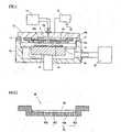
- FIG. 1is an explanation view showing an overall CVD apparatus of the present invention
- FIG. 2is a sectional view of a showerhead of a first embodiment of the present invention
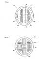
- FIG. 3is a bottom view of a shower plate, in which gas diffusion holes are arranged;
- FIG. 4is a bottom view of the shower plate
- FIG. 5is a bottom view of the shower plate
- FIG. 6is a bottom view of the shower plate
- FIG. 7Ais a sectional view of a modified showerhead
- FIG. 7Bis a sectional view of another modified showerhead
- FIG. 8Ais a sectional view of further modified showerhead
- FIG. 8Bis a sectional view of further modified showerhead
- FIG. 9is a sectional view of a showerhead of a second embodiment
- FIG. 10Ais a plain view of the showerhead, in which gas diffusion holes are arranged;
- FIG. 10Bis a partial enlarged view of the showerhead shown in FIG. 10A ;
- FIG. 11Ais a sectional view of a showerhead of a third embodiment
- FIG. 11Bis a plan view of the showerhead of the third embodiment.
- FIG. 12is an explanation view of the CVD apparatus to which the showerhead shown in FIGS. 11A and 11B is attached.
- FIG. 1is an explanation view showing an overall CVD apparatus relating to the present invention.
- the CVD apparatushas a process chamber 10 , in which a film is formed on a surface of a workpiece 20 .
- a showerhead 40is disposed to face the workpiece 20 , and plasma is generated therein so as to form the film on the surface of the workpiece 20 .
- a plate-shaped electrode 12 for applying RF wavesis attached to an upper part of the chamber 10 .
- the electrode 12 and the chamber 10are electrically insulated by an insulation member 13 .
- O-rings 14 a and 14 bare respectively provided to a contact part between the insulation member 13 and the chamber 10 and a contact part between the insulation member 13 and the electrode 12 .
- the electrode 12is attached to the chamber 10 and air-tightly sealed.
- the electrode 12is connected to an RF generator 15 having a matching circuit.
- the RF generator 15applies prescribed RF waves to the electrode 12 for forming a film.
- a gas inlet 12 ais formed in the electrode 12 so as to supply a process gas for forming the film.
- a tube for supplying the gas to the electrode 12is connected to a gas source 16 and the gas inlet 12 a .
- the tubeis electrically insulated.
- a showerhead 40is fixed to a bottom face of the electrode 12 .
- the gas inlet 12 ais located at the center of the showerhead 40 .
- the showerhead 40comprises: a shower plate 42 having a plate section, which is formed like a flat plate and in which a plurality of gas diffusion holes 42 a penetrate in the thickness direction; and a porous plate 44 provided on an upper face of the shower plate 42 .
- the porous plate 44is formed into a flat plate and made of a porous ceramic or a porous metal.
- the porous plate 44entirely covers the upper face of the plate section of the shower plate 42 so as to cover all of the gas diffusion holes 42 a of the shower plate 42 .
- the showerhead 40is attached to an inner face of the electrode 12 , and an upper face of the porous plate 44 is slightly separated from an inner face of the chamber 10 .
- a space A enclosed by the showerhead 40 and the inner face of the chamber 10acts as a gas introduction space for introducing the gas for forming the film to the showerhead 40 .
- the workpiece 20is supported on a base 22 facing the showerhead 40 .
- a shielding plate 23encloses the base 22 but is separated from an outer side face of the base 22 .
- a discharge port 24is opened in a lower side part of the chamber 10 so as to vacuum-discharge air therefrom.
- a vacuum pump 25is connected to the discharge port 24 .
- the most characteristic point of the CVD apparatusis the showerhead 40 facing the workpiece 20 .
- FIG. 2is an enlarged sectional view of the showerhead 40 .
- the shower plate 42 of the showerhead 40comprises: a plate section 421 , which is formed into a flat plate and disposed to face the workpiece 20 ; and a flange section 422 extended from an outer edge of the plate section 421 .
- the flange section 422is used for attaching the showerhead 40 to the electrode 12 .
- the shower plate 42is made of an electric conductive material, e.g., metal.
- a plurality of the gas diffusion holes 42 apenetrate the plate section 421 in the thickness direction.
- Ratio of the width W of the gas diffusion hole 42 a to the depth H thereofis 1:1-1:10.
- the depth H and the width W of the gas diffusion holes 42 a and distances between the gas diffusion holes 42 amay be optionally designed.
- the width Wis 1.27 mm; the depth H is 3.8 mm; and the distances between the gas diffusion holes 42 a are 3.8 mm.
- the valuesare optimum when process pressure is about 1 Torr.
- the width Wis made narrower and the depth H is made shallower when the process pressure is higher; the width W is made wider and the depth H is made deeper when the process pressure is lower.
- the gas diffusion holes 42 aare straight through-holes, whose inner faces are perpendicular to a surface of the plate section 421 .
- the gas diffusion holes 42 amay be female-tapered holes, each of whose diameter is gradually increased toward the lower end and whose inner faces are inclined about 5 degrees with respect to the vertical line.
- FIG. 3is a bottom view of the shower plate 42 .
- the gas diffusion holes 42are straight elongate holes in plan view and arranged in parallel in the plate section 421 of the shower plate 42 .
- Each of the gas diffusion holes 42 ais a narrow elongate hole whose longitudinal ends are closed. Ratio of the width W of the gas diffusion hole 42 a to the length L thereof is 1:2-1:20.
- the gas diffusion holes 42 amay be optionally arranged in the plate section 421 . Examples of arrangement of the gas diffusion holes 42 a are shown in FIGS. 4-6 . In FIG. 4 , groups of the gas diffusion holes 42 a , which are arranged in the longitudinal direction, and groups of the gas diffusion holes 42 a , which are arranged in the transverse direction, are combined in the shower plate 42 . Groups of the gas diffusion holes 42 a are perpendicularly arranged, but they may be obliquely arranged.
- the gas diffusion holes 42 aare formed into circular arcs and coaxially arranged with respect to the center of the plate section 421 .
- the gas diffusion holes 42 a formed in the plate section 421 of the shower plate 42are elongate holes, dissociation of the gas can be accelerated and gas ionization efficiency can be increased.
- the gas ionization efficiencycan be improved by combining the porous plate 44 and the shower plate 42 .
- the gas diffusion holes 42 amay be formed into not only the elongate holes but also circular holes and polygonal holes. However, in comparison with the elongate holes, the gas ionization efficiency of the circular holes or the polygonal holes is reduced to about 40%.
- the shapes of the gas diffusion holes 42 a and the arrangement thereof in the shower plate 42are optionally designed according to the size and shape of the workpiece 20 and a distance between the workpiece 20 and the showerhead 40 .
- the porous plate 44 of the showerhead 40supplies the process gas, which has been fed to the rear side of the showerhead 40 , to the gas diffusion holes 42 a of the shower plate 42 .
- the porous plate 44is made of a porous ceramic or a porous metal.
- the porous plate 44is a flat plate capable of covering the entire upper face of the shower plate 42 .
- the gas introduced from the gas inlet 12 ais supplied to the gas diffusion holes 42 a through the porous plate 44 . With this action, the gas can be uniformly supplied into the gas diffusion holes 42 a.
- the porous plate 44may be made of a ceramic material, e.g., Al203, Y20, Si3N4. Pore diameters of the porous ceramic material are 0.5-100 ⁇ m, preferably 10-50 ⁇ m.
- the porous plate 44is produced by sintering Al, stainless steel, etc. Pore diameters of the porous metal are 0.5-100 ⁇ m.
- the porous plate 44supplies the gas, which has been introduced to the rear side of the showerhead 40 from the gas inlet 12 a , into the gas diffusion holes 42 a .
- the gas inlet 12 ais opened at the center of the rear face of the showerhead 40 .
- FIGS. 7A and 7Bshow the porous plates 44 capable of restraining the gas-density fluctuation, which is caused by the arrangement of the gas diffusion holes 42 a.
- a center part of the porous plate 44is thicker than other parts.
- gas permeability in the center partcan be lower than that in a perimeter part, so that the gas-density fluctuation can be restrained.
- the center part of the porous plate 44is a thicker section 44 a ; the part on the outer side of the thick section 44 a is a thin section 44 b , whose thickness is gradually reduced toward an outer end.
- the gas permeabilityis reduced by thickening the porous plate 44 . Therefore, the gas can be uniformly supplied to the gas diffusion holes 42 a by adjusting the thickness of the porous plate 44 on the basis of the gas-density fluctuation.
- the amount of the gas supplied to the gas diffusion holes 42 ais adjusted by changing density of the porous plate 44 in a planar area. Porous degree of the porous plate 44 and distribution of material density can be controlled by adjusting a grain size of a material to be sintered and sintering conditions.
- the density of the center part of the porous plate 44is higher than the perimeter part thereof, so that the gas permeability of the center part of the porous plate 44 , in which the gas density is high, is restrained. Therefore, the amount of gas permeation through the gas diffusion holes 42 a can be uniform across the entire porous plate 44 .
- the density of the porous plate 44is made highest in a center part 441 and reduced stepwise toward perimeter parts 442 and 443 . Further, the density of the porous plate 44 may be gradually reduced from the center part to an outer end.
- FIG. 8AMeans for solving this problem is shown in FIG. 8A .
- an O-ring 45having heat resistance and chemical resistance is attached to the perimeter section of the porous plate 44 , which surrounds the gas diffusion hole area in which the gas diffusion holes 42 a are formed. Therefore, a space between the porous plate 44 and the shower plate 42 is sealed when the porous plate 44 is attached to the shower plate 42 .
- the perimeter section 444 of the porous plate 44which has a prescribed width and surrounds the gas diffusion hole area, is a high density section which is not gas-permeable.
- the perimeter section 444is sintered with high density, so that the gas cannot invade into the porous plate 44 .
- a contact face of the perimeter section 444 of the porous plate 44prevents the gas from invading into the space between the porous plate 44 and the shower plate 42 .
- a porous sintered ceramic or metalis suitably used as the material of the porous plate 44 , but the material is not limited to them.
- other porous materialse.g., organic porous film, may be used as the material of the porous plate 44 .
- the porous filmwhich cannot be attached by its own weight, the film is stretched and attached to a rear face of the plate section 421 of the shower plate 42 .
- the porous filmis also considered as the porous plate.
- a metal plate 50is used instead of the porous plate 44 .
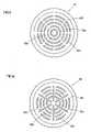
- FIGS. 9 , 10 A and 10 BThe showerhead 40 having the metal plate 50 is shown in FIGS. 9 , 10 A and 10 B.
- FIG. 9is a sectional view of the showerhead 40 .
- the metal plate 50 having gas holes 51is set on the plate section 421 of the shower plate 42 , which has the gas diffusion holes 42 a as well as the first embodiment.
- Each of the gas holes 51is constituted by: a vertical hole 52 penetrating through the metal plate 50 in the thickness direction; and communication grooves 54 being formed in a lower surface of the metal plate 50 so as to communicate with the gas diffusion holes 42 a.
- the vertical holes 52are arranged so as not to correspond to the gas diffusion holes 42 a .
- each of the vertical holes 52is located between the adjacent gas diffusion holes 42 a and covered with the plate section 421 of the shower plate 42 .
- the communication grooves 54are extended from the vertical holes 52 until reaching the gas diffusion holes 42 a , so that the vertical holes 52 can be communicated with the gas diffusion holes 42 a.
- FIG. 10Ais a plan view showing the planar arrangement of the gas diffusion holes 42 a of the shower plate 42 and the gas holes 51 of the metal plate 50 .
- FIG. 10Bis an enlarged view showing the arrangement of the gas holes 51 .
- each gas hole 51is located at a midpoint between the adjacent gas diffusion holes 42 a , and a plurality of the communication grooves 54 are extended from the vertical hole 52 until reaching the adjacent gas diffusion holes 42 a .
- a plurality of the communication grooves 54are communicated with each of the gas diffusion holes 42 a . Therefore, the process gas is supplied to the gas diffusion holes 42 a via the vertical holes 52 and the communication grooves 54 .
- the gas introduced from the gas inlet 12 amust be uniformly supplied to the gas diffusion holes 42 a of the showerhead 40 .
- the communication grooves 54 of the gas holes 51are made narrow so as to uniformly supply the gas to the gas diffusion holes 42 a of the shower plate 42 .
- the vertical holes 52 formed in the metal plate 50need not be made narrow because the gas flow is limited by the communication grooves 54 .
- the vertical holes 52may be relatively wide because the gas is supplied to the gas diffusion holes 42 a via the communication grooves 54 .
- a large number of small gas diffusion holesneed not be formed, so the metal plate 50 can be easily produced.
- the process gaswhich has been supplied into the gas diffusion holes 42 a via the gas holes 51 , collides with the inner faces of the gas diffusion holes 42 a . Therefore, the gas is scattered and reflected, so that the gas can be easily ionized and the film can be efficiently formed.
- a showerhead 60 of the present embodimentis characterized by a porous main body made of a sintered metal.
- FIG. 11Ais a sectional view of the showerhead 60 .
- the showerhead 60comprises: a plate section 601 ; and a flange section 602 , which is extended from an outer edge of the plate section 601 .
- the flange section 602is attached to the electrode 12 , and a gas introduction space is formed on the rear side of the plate section 601 .
- a plurality of gas diffusion grooves 60 aare formed in a surface of the plate section 601 , which faces the workpiece 20 .
- the gas diffusion holes 42 a of the shower plate 42are through-holes penetrating the plate section 421 in the thickness direction; the gas diffusion grooves 60 a are grooves whose upper parts are closed.
- the shower plate 42 and the porous plate 44are combined so as to close the upper parts of the gas diffusion holes 42 a like grooves.
- the gas diffusion grooves 60 aare formed in the main body part of the showerhead 60 .
- FIG. 11Bis a plan view showing the planar arrangement of the gas diffusion grooves 60 a of the showerhead 60 , wherein the gas diffusion grooves 60 a are linear grooves.
- the gas diffusion grooves 60 aare elongate grooves as well as the elongate gas diffusion holes 42 a , so that ionization of the process gas in the gas diffusion grooves 60 a can be accelerated and film-forming efficiency can be improved.
- FIG. 12shows a CVD apparatus, in which the showerhead 60 shown in FIGS. 11A and 11B is attached.
- the showerhead 60is attached to the inner face of the electrode 12 .
- the structure of the CVD apparatusis the same as that shown in FIG. 1 .
- the RF generator 15is electrically connected to the electrode 12 , and RF waves are applied to the showerhead 60 , which is made of an electric conductive material, so as to generate plasma for forming the film.
- the process gas for forming the filmwhich has been supplied to the rear side of the showerhead 60 via the gas inlet 12 a , permeates the porous plate section 601 of the showerhead 60 until reaching the gas diffusion grooves 60 a . Thicknesses of ceiling sections of the gas diffusion grooves 60 a are thinner than a thickness of the plate section 601 , so the gas permeates the ceiling sections and reaches the gas diffusion grooves 60 a . Then, the gas is dissociated in the gas diffusion grooves 60 a.
- the main body part of the showerhead 60made of a porous conductive material, e.g., porous metal
- the main body partcan be formed by compression-molding the material with a molding die and sintering the molded material.
- the showerhead 60can be highly easily produced.
- shapes of the gas diffusion grooves 60 acan be optionally selected by changing the molding die.
- a sectional shape of the plate section 601may be formed into a mountain shape as well as the porous plate 44 shown in FIG. 7A , and density of the plate section 601 may be partially varied as well as the porous plate 44 shown in FIG. 7B .
- the workpiece 20is set on the base 22 so as to face the showerhead 40 .
- the base 22heats the workpiece 20 until reaching reaction temperature.
- the reaction temperatureis about 400° C.
- the distance between the showerhead 40 and the workpiece 20is an important factor to uniformly forming the film on the surface of the workpiece 20 . Further, the size and arrangement of the gas diffusion holes 42 a of the showerhead 40 are also important factors. Therefore, the distance between the showerhead 40 and the workpiece 20 is designed according to other factors, e.g., gas diffusion holes. In case of forming the silicon nitride film, for example, the distance between the showerhead 40 and the workpiece 20 is 6-35 mm.
- the process gas for forming the filmis introduced into the gas introduction space, which is formed on the rear side of the showerhead 40 , via the gas inlet 12 a .
- the gas supplied on the rear side of the showerhead 40permeates the porous plate 44 and reaches the gas diffusion holes 42 a .
- the gasis supplied to the gas diffusion holes 42 a via the gas holes 51 of the metal plate 50 .
- the gaspermeates the plate section 601 and reaches the gas diffusion grooves 60 a.
- the RF generator 15applies RF waves to the showerhead 40 or 60 so as to generate plasma in a space between the workpiece 20 and the showerhead 40 or 60 , so that the film is formed on the surface of the workpiece 20 .
- RF wavesmay be applied to the showerhead 40 or 60 only, or RF waves may be applied to the workpiece 20 (the base 22 ) only. Further, RF waves may be applied to the both of the showerhead 40 or 60 and the workpiece 20 .
- RF waves of higher frequencymay be applied to the showerhead 40 or 60 so as to efficiently dissociate the gas; RF waves of lower frequency (about 500 KHz) may be applied to the workpiece 20 so as to efficiently bombard ions.
- the CVD apparatus of the present inventionmay employ any of the methods.
- the gasBy supplying the process gas to the gas diffusion holes 42 a or the gas diffusion grooves 60 a , the gas can stably charge and is easily dissociated in the groove-shaped spaces. Therefore, even if the gas which is hard to be ionized, e.g., silicon nitride, is used, the film can be efficiently formed.
- the gas which is hard to be ionizede.g., silicon nitride
- SiH4 + NH3, SiH4+N2 and SiH4++NH3+N2may be used as the gas species.
- a preferable frequency of the RF wavesis 2-100 MHz, more preferably 13 MHz.
- a preferable gas pressureis 0.5-4 Torr, more preferably 1 Torr.
- the showerhead of the present inventionhas the groove-shaped gas diffusion spaces, which are formed by the gas diffusion holes 42 a and the porous plate 44 or the gas diffusion grooves 60 a formed in the showerhead itself, so that N2 can be efficiently ionized in the gas diffusion holes or grooves.
- the film-forming efficiency of the CVD apparatuswas 2.5 times greater than that of the conventional CVD apparatus.
- the workpiece 20 used in the CVD apparatus of the present inventionmay be a semiconductor wafer, a solar battery panel, an LCD panel, etc.
- the porous plate 44which is made of a ceramic or a sintered metal, and the showerhead 60 having the porous main body part can be highly cleaned, so they can be suitably used for the film-forming process.
Landscapes
- Chemical & Material Sciences (AREA)
- Engineering & Computer Science (AREA)
- Physics & Mathematics (AREA)
- Plasma & Fusion (AREA)
- General Chemical & Material Sciences (AREA)
- Chemical Kinetics & Catalysis (AREA)
- Materials Engineering (AREA)
- Mechanical Engineering (AREA)
- Metallurgy (AREA)
- Organic Chemistry (AREA)
- Analytical Chemistry (AREA)
- Chemical Vapour Deposition (AREA)
Abstract
Description
- The present invention relates to a showerhead and a CVD (Chemical Vapor Deposition) apparatus using the showerhead.
- In a typical plasma CVD apparatus, a process gas for forming a film is supplied into a chamber, and then RF (Radio Frequency) waves are applied to a showerhead so as to generate plasma and ionize the gas, so that the film is formed on a surface of a workpiece, which is disposed to face the shower head.
- The showerhead of the CVD apparatus is used for efficiently ionizing the gas and uniformly forming the film on the surface of the workpiece. Various of types of showerheads have been provided. A typical showerhead has a plate section, which faces the workpiece and in which gas diffusion holes are formed, and the gas is sprayed from the gas diffusion holes toward the workpiece, so that the gas is dissociated and the film is formed thereon. Further, Japanese Patent Gazettes No. 2003-28142 and No. 2003-7682 disclose showerheads, whose plate sections are made of a porous ceramic; and Japanese Patent Gazette No. 2005-516407 discloses a showerhead, whose plate section has long grooves in which gas diffusion holes are bored.
- In the showerhead having the plate section, a large number (several hundreds to several thousands) of the gas diffusion holes must be formed, so a production cost of the plate section must be increased. Since the gas diffusion holes, whose inner diameters are about 0.2 mm, are manually bored, one by one, by drilling, it takes for a several days to penetrate the gas diffusion holes in one showerhead.
- On the other hand, in comparison with the showerhead in which the gas diffusion holes are bored in the plate section, the showerhead made of the porous ceramic is capable of uniformly spraying the gas, and no gas diffusion holes are manually bored so that a production cost can be lowered. However, in the showerhead made of the porous ceramic, the gas cannot be efficiently ionized, so the showerhead is not suitable for forming a film with gas species which are hard to be ionized, e.g., silicon nitride (SiNx).
- The present invention was conceived to solve the above described problems.
- An object of the present invention is to provide a showerhead for a CVD apparatus, in which a plurality of gas diffusion holes are formed in a plate section, can be easily produced and which is capable of efficiently forming a film with gas species which are hard to be ionized, e.g., silicon nitride (SiNx).
- Another object is to provide a CVD apparatus using said showerhead.
- To achieve the objects, the present invention has following structures.
- Namely, the showerhead for a CVD apparatus comprises:
- a shower plate being made of a metal; and
- a porous plate contacting a rear face of the shower plate,
- a plurality of gas diffusion holes are formed in a plate section of the shower plate, which faces a workpiece, and penetrate the plate section in the thickness direction, and
- the porous plate covers all of the gas diffusion holes.
- In the showerhead, the gas diffusion holes may be elongate holes. With this structure, a gas can be efficiently ionized, so that a film can be efficiently formed. Note that, planar shapes of the elongated holes may be long linear holes and long curved holes.
- In the showerhead, a thickness of the porous plate may be thicker in a high gas-density area of a gas introduction space, which is formed on the rear side of the shower head, so that the amount of gas permeation through the gas diffusion holes is uniform across the entire showerhead. Further, density of the porous plate may be higher in a high gas-density area of a gas introduction space, which is formed on the rear side of the shower head, so that the amount of gas permeation through the gas diffusion holes is uniform across the entire showerhead. In these cases, the gas density on the rear side of the showerhead can be made uniform, so that the film can be uniformly formed.
- In the showerhead, the porous plate may have a perimeter section, which surrounds a gas diffusion hole area and which is not gas-permeable. With this structure, no gas invades into the gas diffusion holes via the contact part between the porous plate and the shower plate, so that the film can be more suitably formed.
- In the showerhead, a metal plate may be installed instead of the porous plate, and the metal plate may have: vertical holes penetrating through the metal plate in the thickness direction; and communicating grooves being formed in a surface of the metal plate, which contacts the plate section of the shower plate, the communicating grooves mutually communicating the gas diffusion holes. With this structure, the gas for forming the film can be uniformly supplied to the gas diffusion holes, so that the film can be formed suitably.
- Another showerhead for a CVD apparatus comprises a main body part being made of a metallic porous material, and
- a plurality of gas diffusion grooves are formed in a plate section of the main body part, which faces a workpiece.
- In the showerhead, the gas diffusion grooves may be elongated grooves in plan view. With this structure, the supplied gas can be efficiently ionized, and film-forming efficiency can be improved.
- In the showerhead, a thickness of the main body part may be thicker in a high gas-density area of a gas introduction space, which is formed on the rear side of the shower head, so that the amount of gas permeation through the gas diffusion grooves is uniform across the entire main body part. Further, density of the main body part may be higher in a high gas-density area of a gas introduction space, which is formed on the rear side of the shower head, so that the amount of gas permeation through the gas diffusion grooves is uniform across the entire main body part. With these structures, the film can be uniformly formed on the surface of the workpiece.
- Further, the CVD apparatus of the present invention comprises:
- a process chamber;
- a showerhead being provided in the process chamber and facing a workpiece;
- a gas inlet for supplying a gas, which is used for forming a nitride film on the surface of the workpiece, to the showerhead, the gas inlet being formed in a rear face of the showerhead,
- plasma for forming the film on the workpiece is generated between the showerhead and the workpiece by applying RF waves therebetween,
- the showerhead comprises: a shower plate being made of a metal; and a porous plate being disposed to contact a rear face of the shower plate, and
- a plurality of gas diffusion holes are formed in a plate section of the shower plate, which faces the workpiece, and penetrate the plate section in the thickness direction, and
- the porous plate covers all of the gas diffusion holes.
- Another CVD apparatus comprises:
- a process chamber;
- a showerhead being provided in the process chamber and facing a workpiece;
- a gas inlet for supplying a gas, which is used for forming a nitride film on the surface of the workpiece, to the showerhead, the gas inlet being formed in a rear face of the showerhead,
- plasma for forming the film on the workpiece is generated between the showerhead and the workpiece by applying RF waves therebetween,
- the showerhead comprises a main body part being made of a metallic porous material, and
- a plurality of gas diffusion grooves are formed in a plate section of the main body part, which faces the workpiece. With this structure, gasses, which are hard to be ionized, can be efficiently dissociated, so that film-forming efficiency of the CVD apparatus can be improved.
- The showerhead of the present invention is constituted by the shower plate having the gas diffusion holes and the porous plate, or by the porous main body part having the gas diffusion grooves, so ionization efficiency of the showerhead can be substantially increased. By supplying the gas through the porous member, the gas can be uniformly supplied. Therefore, even if gas species, which are hard to be ionized, are used, the showerhead is capable of highly efficiently forming the film. Further, by using the porous plate or the porous main body part, the showerhead can be easily produced, a production cost of the showerhead can be reduced, and a production time thereof can be shortened.
- Embodiments of the present invention will now be described by way of examples and with reference to the accompanying drawings, in which:
FIG. 1 is an explanation view showing an overall CVD apparatus of the present invention;FIG. 2 is a sectional view of a showerhead of a first embodiment of the present invention;FIG. 3 is a bottom view of a shower plate, in which gas diffusion holes are arranged;FIG. 4 is a bottom view of the shower plate;FIG. 5 is a bottom view of the shower plate;FIG. 6 is a bottom view of the shower plate;FIG. 7A is a sectional view of a modified showerhead;FIG. 7B is a sectional view of another modified showerhead;FIG. 8A is a sectional view of further modified showerhead;FIG. 8B is a sectional view of further modified showerhead;FIG. 9 is a sectional view of a showerhead of a second embodiment;FIG. 10A is a plain view of the showerhead, in which gas diffusion holes are arranged;FIG. 10B is a partial enlarged view of the showerhead shown inFIG. 10A ;FIG. 11A is a sectional view of a showerhead of a third embodiment;FIG. 11B is a plan view of the showerhead of the third embodiment; andFIG. 12 is an explanation view of the CVD apparatus to which the showerhead shown inFIGS. 11A and 11B is attached.- Preferred embodiments of the present invention will now be described in detail with reference to the accompanying drawings.
FIG. 1 is an explanation view showing an overall CVD apparatus relating to the present invention. The CVD apparatus has aprocess chamber 10, in which a film is formed on a surface of aworkpiece 20. In thechamber 10, ashowerhead 40 is disposed to face theworkpiece 20, and plasma is generated therein so as to form the film on the surface of theworkpiece 20.- A plate-shaped
electrode 12 for applying RF waves is attached to an upper part of thechamber 10. Theelectrode 12 and thechamber 10 are electrically insulated by aninsulation member 13. O-rings insulation member 13 and thechamber 10 and a contact part between theinsulation member 13 and theelectrode 12. Theelectrode 12 is attached to thechamber 10 and air-tightly sealed. - The
electrode 12 is connected to anRF generator 15 having a matching circuit. TheRF generator 15 applies prescribed RF waves to theelectrode 12 for forming a film. - A
gas inlet 12ais formed in theelectrode 12 so as to supply a process gas for forming the film. A tube for supplying the gas to theelectrode 12 is connected to agas source 16 and thegas inlet 12a. The tube is electrically insulated. - A
showerhead 40 is fixed to a bottom face of theelectrode 12. Thegas inlet 12ais located at the center of theshowerhead 40. - The
showerhead 40 comprises: ashower plate 42 having a plate section, which is formed like a flat plate and in which a plurality of gas diffusion holes42apenetrate in the thickness direction; and aporous plate 44 provided on an upper face of theshower plate 42. - The
porous plate 44 is formed into a flat plate and made of a porous ceramic or a porous metal. Theporous plate 44 entirely covers the upper face of the plate section of theshower plate 42 so as to cover all of the gas diffusion holes42aof theshower plate 42. - The
showerhead 40 is attached to an inner face of theelectrode 12, and an upper face of theporous plate 44 is slightly separated from an inner face of thechamber 10. A space A enclosed by theshowerhead 40 and the inner face of thechamber 10 acts as a gas introduction space for introducing the gas for forming the film to theshowerhead 40. - The
workpiece 20 is supported on a base22 facing theshowerhead 40. A shieldingplate 23 encloses the base22 but is separated from an outer side face of thebase 22. Adischarge port 24 is opened in a lower side part of thechamber 10 so as to vacuum-discharge air therefrom. Avacuum pump 25 is connected to thedischarge port 24. - The most characteristic point of the CVD apparatus is the
showerhead 40 facing theworkpiece 20. FIG. 2 is an enlarged sectional view of theshowerhead 40. Theshower plate 42 of theshowerhead 40 comprises: aplate section 421, which is formed into a flat plate and disposed to face theworkpiece 20; and aflange section 422 extended from an outer edge of theplate section 421. Theflange section 422 is used for attaching theshowerhead 40 to theelectrode 12. Theshower plate 42 is made of an electric conductive material, e.g., metal.- As described above, a plurality of the gas diffusion holes42apenetrate the
plate section 421 in the thickness direction. Ratio of the width W of thegas diffusion hole 42ato the depth H thereof is 1:1-1:10. By making the depth H equal to or greater than the width W, ionizing the gas in thegas diffusion layer 42acan be accelerated and film-forming efficiency can be improved. The depth H and the width W of the gas diffusion holes42aand distances between the gas diffusion holes42amay be optionally designed. For example, the width W is 1.27 mm; the depth H is 3.8 mm; and the distances between the gas diffusion holes42aare 3.8 mm. The values are optimum when process pressure is about 1 Torr. Preferably, the width W is made narrower and the depth H is made shallower when the process pressure is higher; the width W is made wider and the depth H is made deeper when the process pressure is lower. - In the present embodiment, the gas diffusion holes42aare straight through-holes, whose inner faces are perpendicular to a surface of the
plate section 421. In another case, the gas diffusion holes42amay be female-tapered holes, each of whose diameter is gradually increased toward the lower end and whose inner faces are inclined about 5 degrees with respect to the vertical line. FIG. 3 is a bottom view of theshower plate 42. The gas diffusion holes42 are straight elongate holes in plan view and arranged in parallel in theplate section 421 of theshower plate 42. Each of the gas diffusion holes42ais a narrow elongate hole whose longitudinal ends are closed. Ratio of the width W of thegas diffusion hole 42ato the length L thereof is 1:2-1:20. By the elongate gas diffusion holes42a, the gas, which has been supplied from the rear side of theshowerhead 40 into the gas diffusion holes42a, collides with the inner faces of the gas diffusion holes42a. Therefore, the gas is scattered and reflected, so that the gas can be easily ionized.- The gas diffusion holes42amay be optionally arranged in the
plate section 421. Examples of arrangement of the gas diffusion holes42aare shown inFIGS. 4-6 . InFIG. 4 , groups of the gas diffusion holes42a, which are arranged in the longitudinal direction, and groups of the gas diffusion holes42a, which are arranged in the transverse direction, are combined in theshower plate 42. Groups of the gas diffusion holes42aare perpendicularly arranged, but they may be obliquely arranged. - In
FIG. 5 , the gas diffusion holes42aare formed into circular arcs and coaxially arranged with respect to the center of theplate section 421. - In
FIG. 6 , the coaxial gas diffusion holes42aformed into circular arcs and the linear gas diffusion holes42aradially extended from the center of theplate section 421 are combined. - Since the gas diffusion holes42aformed in the
plate section 421 of theshower plate 42 are elongate holes, dissociation of the gas can be accelerated and gas ionization efficiency can be increased. The gas ionization efficiency can be improved by combining theporous plate 44 and theshower plate 42. The gas diffusion holes42amay be formed into not only the elongate holes but also circular holes and polygonal holes. However, in comparison with the elongate holes, the gas ionization efficiency of the circular holes or the polygonal holes is reduced to about 40%. - The shapes of the gas diffusion holes42aand the arrangement thereof in the
shower plate 42 are optionally designed according to the size and shape of theworkpiece 20 and a distance between the workpiece20 and theshowerhead 40. - The
porous plate 44 of theshowerhead 40 supplies the process gas, which has been fed to the rear side of theshowerhead 40, to the gas diffusion holes42aof theshower plate 42. Theporous plate 44 is made of a porous ceramic or a porous metal. Theporous plate 44 is a flat plate capable of covering the entire upper face of theshower plate 42. The gas introduced from thegas inlet 12ais supplied to the gas diffusion holes42athrough theporous plate 44. With this action, the gas can be uniformly supplied into the gas diffusion holes42a. - For example, the
porous plate 44 may be made of a ceramic material, e.g., Al203, Y20, Si3N4. Pore diameters of the porous ceramic material are 0.5-100 μm, preferably 10-50 μm. - In case of using the
porous plate 44 made of the porous metal, theporous plate 44 is produced by sintering Al, stainless steel, etc. Pore diameters of the porous metal are 0.5-100 μm. - The
porous plate 44 supplies the gas, which has been introduced to the rear side of theshowerhead 40 from thegas inlet 12a, into the gas diffusion holes42a. Thegas inlet 12ais opened at the center of the rear face of theshowerhead 40. With this structure, gas density in the gas introduction space of theshowerhead 40 is increased in the center part; the gas density is reduced in a peripheral part. Namely, the gas density in the gas introduction space is fluctuated. By the gas-density fluctuation, it is difficult to uniformly form the film on the surface of theworkpiece 20. FIGS. 7A and 7B show theporous plates 44 capable of restraining the gas-density fluctuation, which is caused by the arrangement of the gas diffusion holes42a.- In
FIG. 7A , a center part of theporous plate 44 is thicker than other parts. With this structure, gas permeability in the center part can be lower than that in a perimeter part, so that the gas-density fluctuation can be restrained. The center part of theporous plate 44 is athicker section 44a; the part on the outer side of thethick section 44ais athin section 44b, whose thickness is gradually reduced toward an outer end. The gas permeability is reduced by thickening theporous plate 44. Therefore, the gas can be uniformly supplied to the gas diffusion holes42aby adjusting the thickness of theporous plate 44 on the basis of the gas-density fluctuation. - In
FIG. 7B , the amount of the gas supplied to the gas diffusion holes42ais adjusted by changing density of theporous plate 44 in a planar area. Porous degree of theporous plate 44 and distribution of material density can be controlled by adjusting a grain size of a material to be sintered and sintering conditions. Thus, the density of the center part of theporous plate 44 is higher than the perimeter part thereof, so that the gas permeability of the center part of theporous plate 44, in which the gas density is high, is restrained. Therefore, the amount of gas permeation through the gas diffusion holes42acan be uniform across the entireporous plate 44. InFIG. 7B , the density of theporous plate 44 is made highest in acenter part 441 and reduced stepwise towardperimeter parts porous plate 44 may be gradually reduced from the center part to an outer end. - In case of attaching the
porous plate 44 to theshower plate 42 to uniformly supplying the gas to the gas diffusion holes42a, there is a problem of sealing the perimeter section of theporous plate 44 and theplate section 421 of theshower plate 42. In the vicinity of the perimeter section of theporous plate 44, the gas moves toward a lower face of theporous plate 44, so the gas cannot be uniformly supplied. - Means for solving this problem is shown in
FIG. 8A . In the upper face of theplate section 421 of theshower plate 42, an O-ring 45 having heat resistance and chemical resistance is attached to the perimeter section of theporous plate 44, which surrounds the gas diffusion hole area in which the gas diffusion holes42aare formed. Therefore, a space between theporous plate 44 and theshower plate 42 is sealed when theporous plate 44 is attached to theshower plate 42. - Another means is shown in
FIG. 8B . Theperimeter section 444 of theporous plate 44, which has a prescribed width and surrounds the gas diffusion hole area, is a high density section which is not gas-permeable. Theperimeter section 444 is sintered with high density, so that the gas cannot invade into theporous plate 44. A contact face of theperimeter section 444 of theporous plate 44 prevents the gas from invading into the space between theporous plate 44 and theshower plate 42. - A porous sintered ceramic or metal is suitably used as the material of the
porous plate 44, but the material is not limited to them. For example, other porous materials, e.g., organic porous film, may be used as the material of theporous plate 44. In case of using, for example, the porous film which cannot be attached by its own weight, the film is stretched and attached to a rear face of theplate section 421 of theshower plate 42. In the present invention, the porous film is also considered as the porous plate. - In the showerhead of a second embodiment, a
metal plate 50 is used instead of theporous plate 44. - The
showerhead 40 having themetal plate 50 is shown inFIGS. 9 ,10A and10B.FIG. 9 is a sectional view of theshowerhead 40. In the present embodiment, themetal plate 50 havinggas holes 51 is set on theplate section 421 of theshower plate 42, which has the gas diffusion holes42aas well as the first embodiment. - Each of the gas holes51 is constituted by: a
vertical hole 52 penetrating through themetal plate 50 in the thickness direction; andcommunication grooves 54 being formed in a lower surface of themetal plate 50 so as to communicate with the gas diffusion holes42a. - The
vertical holes 52 are arranged so as not to correspond to the gas diffusion holes42a. In another words, each of thevertical holes 52 is located between the adjacent gas diffusion holes42aand covered with theplate section 421 of theshower plate 42. - On the other hand, the
communication grooves 54 are extended from thevertical holes 52 until reaching the gas diffusion holes42a, so that thevertical holes 52 can be communicated with the gas diffusion holes42a. FIG. 10A is a plan view showing the planar arrangement of the gas diffusion holes42aof theshower plate 42 and the gas holes51 of themetal plate 50.FIG. 10B is an enlarged view showing the arrangement of the gas holes51.- The
vertical hole 52 of eachgas hole 51 is located at a midpoint between the adjacent gas diffusion holes42a, and a plurality of thecommunication grooves 54 are extended from thevertical hole 52 until reaching the adjacent gas diffusion holes42a. A plurality of thecommunication grooves 54 are communicated with each of the gas diffusion holes42a. Therefore, the process gas is supplied to the gas diffusion holes42avia thevertical holes 52 and thecommunication grooves 54. - The gas introduced from the
gas inlet 12amust be uniformly supplied to the gas diffusion holes42aof theshowerhead 40. In the present embodiment, thecommunication grooves 54 of the gas holes51 are made narrow so as to uniformly supply the gas to the gas diffusion holes42aof theshower plate 42. - On the other hand, the
vertical holes 52 formed in themetal plate 50 need not be made narrow because the gas flow is limited by thecommunication grooves 54. Thevertical holes 52 may be relatively wide because the gas is supplied to the gas diffusion holes42avia thecommunication grooves 54. Unlike the conventional showerhead, a large number of small gas diffusion holes need not be formed, so themetal plate 50 can be easily produced. - In the
showerhead 40 of the present embodiment too, the process gas, which has been supplied into the gas diffusion holes42avia the gas holes51, collides with the inner faces of the gas diffusion holes42a. Therefore, the gas is scattered and reflected, so that the gas can be easily ionized and the film can be efficiently formed. - The showerhead of the third embodiment is shown in
FIGS. 11A and 11B . Ashowerhead 60 of the present embodiment is characterized by a porous main body made of a sintered metal. FIG. 11A is a sectional view of theshowerhead 60. Theshowerhead 60 comprises: aplate section 601; and aflange section 602, which is extended from an outer edge of theplate section 601. Theflange section 602 is attached to theelectrode 12, and a gas introduction space is formed on the rear side of theplate section 601.- A plurality of
gas diffusion grooves 60aare formed in a surface of theplate section 601, which faces theworkpiece 20. The gas diffusion holes42aof theshower plate 42 are through-holes penetrating theplate section 421 in the thickness direction; thegas diffusion grooves 60aare grooves whose upper parts are closed. In the above describedshowerhead 40, theshower plate 42 and theporous plate 44 are combined so as to close the upper parts of the gas diffusion holes42alike grooves. On the other hand, in the present embodiment, thegas diffusion grooves 60aare formed in the main body part of theshowerhead 60. - Planar shapes of the
gas diffusion grooves 60a, which are formed in theplate section 601 of theshowerhead 60, are not limited as well as those of the gas diffusion holes42aof the above describedshowerhead 40.FIG. 11B is a plan view showing the planar arrangement of thegas diffusion grooves 60aof theshowerhead 60, wherein thegas diffusion grooves 60aare linear grooves. Thegas diffusion grooves 60aare elongate grooves as well as the elongate gas diffusion holes42a, so that ionization of the process gas in thegas diffusion grooves 60acan be accelerated and film-forming efficiency can be improved. FIG. 12 shows a CVD apparatus, in which theshowerhead 60 shown inFIGS. 11A and 11B is attached. Theshowerhead 60 is attached to the inner face of theelectrode 12. The structure of the CVD apparatus is the same as that shown inFIG. 1 . TheRF generator 15 is electrically connected to theelectrode 12, and RF waves are applied to theshowerhead 60, which is made of an electric conductive material, so as to generate plasma for forming the film.- In the CVD apparatus, the process gas for forming the film, which has been supplied to the rear side of the
showerhead 60 via thegas inlet 12a, permeates theporous plate section 601 of theshowerhead 60 until reaching thegas diffusion grooves 60a. Thicknesses of ceiling sections of thegas diffusion grooves 60aare thinner than a thickness of theplate section 601, so the gas permeates the ceiling sections and reaches thegas diffusion grooves 60a. Then, the gas is dissociated in thegas diffusion grooves 60a. - In case of using the main body part of the
showerhead 60 made of a porous conductive material, e.g., porous metal, the main body part can be formed by compression-molding the material with a molding die and sintering the molded material. Unlike the conventional showerhead in which a large number of small holes are bored by drilling, theshowerhead 60 can be highly easily produced. Further, shapes of thegas diffusion grooves 60acan be optionally selected by changing the molding die. - In the CVD apparatus, a sectional shape of the
plate section 601 may be formed into a mountain shape as well as theporous plate 44 shown inFIG. 7A , and density of theplate section 601 may be partially varied as well as theporous plate 44 shown inFIG. 7B . With these structures, gas-density variance in thegas diffusion grooves 60a, which is caused by gas-density fluctuation in the gas introduction space of theshowerhead 60, can be restrained. - Next, the process of forming the film on the surface of the
workpiece 20 with the above described CVD apparatus will be explained. - As shown in
FIG. 1 , theworkpiece 20 is set on the base22 so as to face theshowerhead 40. The base22 heats theworkpiece 20 until reaching reaction temperature. In case of forming a nitride film, e.g., silicon nitride film, the reaction temperature is about 400° C. - The distance between the
showerhead 40 and theworkpiece 20 is an important factor to uniformly forming the film on the surface of theworkpiece 20. Further, the size and arrangement of the gas diffusion holes42aof theshowerhead 40 are also important factors. Therefore, the distance between theshowerhead 40 and theworkpiece 20 is designed according to other factors, e.g., gas diffusion holes. In case of forming the silicon nitride film, for example, the distance between theshowerhead 40 and theworkpiece 20 is 6-35 mm. - Firstly, the process gas for forming the film is introduced into the gas introduction space, which is formed on the rear side of the
showerhead 40, via thegas inlet 12a. The gas supplied on the rear side of theshowerhead 40 permeates theporous plate 44 and reaches the gas diffusion holes42a. On the other hand, in theshowerhead 40 having themetal plate 50, the gas is supplied to the gas diffusion holes42avia the gas holes51 of themetal plate 50. Further, in theshowerhead 60 having the porous main body part, the gas permeates theplate section 601 and reaches thegas diffusion grooves 60a. - The
RF generator 15 applies RF waves to theshowerhead showerhead workpiece 20. There are several methods for applying RF waves. Namely, RF waves may be applied to theshowerhead showerhead workpiece 20. In this case, for example, RF waves of higher frequency (about 1.3 MHz) may be applied to theshowerhead workpiece 20 so as to efficiently bombard ions. The CVD apparatus of the present invention may employ any of the methods. - By supplying the process gas to the gas diffusion holes42aor the
gas diffusion grooves 60a, the gas can stably charge and is easily dissociated in the groove-shaped spaces. Therefore, even if the gas which is hard to be ionized, e.g., silicon nitride, is used, the film can be efficiently formed. - For example, in case of forming the silicon nitride film, which will be used as a protection film or an insulation film of a semiconductor device, SiH4+NH3, SiH4+N2 and SiH4++NH3+N2 may be used as the gas species. To efficiently ionize the process gas, a preferable frequency of the RF waves is 2-100 MHz, more preferably 13 MHz. A preferable gas pressure is 0.5-4 Torr, more preferably 1 Torr.
- In case of using the gas of SiH4+N2, N2 must be dissociated, but little N2 is dissociated by the conventional showerhead in which the small gas holes are bored. On the other hand, the showerhead of the present invention has the groove-shaped gas diffusion spaces, which are formed by the gas diffusion holes42aand the
porous plate 44 or thegas diffusion grooves 60aformed in the showerhead itself, so that N2 can be efficiently ionized in the gas diffusion holes or grooves. - In case of using the gas of SiH4+NH3, according to an experiment, the film-forming efficiency of the CVD apparatus was 2.5 times greater than that of the conventional CVD apparatus. By permeating the gas through the porous member, the gas can be uniformly supplied so that the film can be stably and uniformly formed.
- The
workpiece 20 used in the CVD apparatus of the present invention may be a semiconductor wafer, a solar battery panel, an LCD panel, etc. Theporous plate 44, which is made of a ceramic or a sintered metal, and theshowerhead 60 having the porous main body part can be highly cleaned, so they can be suitably used for the film-forming process. - The invention may be embodied in other specific forms without departing from the spirit of essential characteristics thereof. The present embodiments are therefore to be considered in all respects as illustrative and not restrictive, the scope of the invention being indicated by the appended claims rather than by the foregoing description and all changes which come within the meaning and range of equivalency of the claims are therefore intended to be embraced therein.
Claims (12)
Applications Claiming Priority (2)
| Application Number | Priority Date | Filing Date | Title |
|---|---|---|---|
| JP2007-39923 | 2007-02-20 | ||
| JP2007039923AJP2008205219A (en) | 2007-02-20 | 2007-02-20 | Showerhead, and cvd apparatus using the same showerhead |
Publications (1)
| Publication Number | Publication Date |
|---|---|
| US20080196666A1true US20080196666A1 (en) | 2008-08-21 |
Family
ID=39705583
Family Applications (1)
| Application Number | Title | Priority Date | Filing Date |
|---|---|---|---|
| US11/826,336AbandonedUS20080196666A1 (en) | 2007-02-20 | 2007-07-13 | Shower head and cvd apparatus using the same |
Country Status (2)
| Country | Link |
|---|---|
| US (1) | US20080196666A1 (en) |
| JP (1) | JP2008205219A (en) |
Cited By (102)
| Publication number | Priority date | Publication date | Assignee | Title |
|---|---|---|---|---|
| US20100267191A1 (en)* | 2009-04-20 | 2010-10-21 | Applied Materials, Inc. | Plasma enhanced thermal evaporator |
| US20110088847A1 (en)* | 2009-10-15 | 2011-04-21 | Law Kam S | Showerhead assembly for plasma processing chamber |
| US20120097330A1 (en)* | 2010-10-20 | 2012-04-26 | Applied Materials, Inc. | Dual delivery chamber design |
| US20140238608A1 (en)* | 2013-02-28 | 2014-08-28 | Novellus Systems, Inc. | Ceramic showerhead with embedded rf electrode for capacitively coupled plasma reactor |
| US20140271097A1 (en)* | 2013-03-15 | 2014-09-18 | Applied Materials, Inc. | Processing systems and methods for halide scavenging |
| US20140360601A1 (en)* | 2013-06-08 | 2014-12-11 | Everdisplay Optronics (Shanghai) Limited | Upper electrode device |
| WO2015104155A1 (en)* | 2014-01-10 | 2015-07-16 | Aixtron Se | Gas inlet element of a cvd reactor with weight-reduced gas outlet plate |
| CN104870687A (en)* | 2012-12-21 | 2015-08-26 | 吉列公司 | Chemical vapor deposition of fluorocarbon polymers |
| US9175393B1 (en) | 2011-08-31 | 2015-11-03 | Alta Devices, Inc. | Tiled showerhead for a semiconductor chemical vapor deposition reactor |
| US9212422B2 (en) | 2011-08-31 | 2015-12-15 | Alta Devices, Inc. | CVD reactor with gas flow virtual walls |
| US9267205B1 (en) | 2012-05-30 | 2016-02-23 | Alta Devices, Inc. | Fastener system for supporting a liner plate in a gas showerhead reactor |
| US9287152B2 (en) | 2009-12-10 | 2016-03-15 | Orbotech LT Solar, LLC. | Auto-sequencing multi-directional inline processing method |
| US9462921B2 (en) | 2011-05-24 | 2016-10-11 | Orbotech LT Solar, LLC. | Broken wafer recovery system |
| US20170211185A1 (en)* | 2016-01-22 | 2017-07-27 | Applied Materials, Inc. | Ceramic showerhead with embedded conductive layers |
| US9790596B1 (en)* | 2013-01-30 | 2017-10-17 | Kyocera Corporation | Gas nozzle and plasma device employing same |
| US10100408B2 (en) | 2014-03-03 | 2018-10-16 | Applied Materials, Inc. | Edge hump reduction faceplate by plasma modulation |
| US10128086B1 (en) | 2017-10-24 | 2018-11-13 | Applied Materials, Inc. | Silicon pretreatment for nitride removal |
| US10163696B2 (en) | 2016-11-11 | 2018-12-25 | Applied Materials, Inc. | Selective cobalt removal for bottom up gapfill |
| US10170336B1 (en) | 2017-08-04 | 2019-01-01 | Applied Materials, Inc. | Methods for anisotropic control of selective silicon removal |
| US10186428B2 (en) | 2016-11-11 | 2019-01-22 | Applied Materials, Inc. | Removal methods for high aspect ratio structures |
| US20190032246A1 (en)* | 2015-02-16 | 2019-01-31 | Advanced Micro-Fabrication Equipment Inc, Shanghai | Process component and method to improve mocvd reaction process |
| US10224182B2 (en) | 2011-10-17 | 2019-03-05 | Novellus Systems, Inc. | Mechanical suppression of parasitic plasma in substrate processing chamber |
| US10224180B2 (en) | 2016-10-04 | 2019-03-05 | Applied Materials, Inc. | Chamber with flow-through source |
| US10224210B2 (en) | 2014-12-09 | 2019-03-05 | Applied Materials, Inc. | Plasma processing system with direct outlet toroidal plasma source |
| US10242908B2 (en) | 2016-11-14 | 2019-03-26 | Applied Materials, Inc. | Airgap formation with damage-free copper |
| US10256079B2 (en) | 2013-02-08 | 2019-04-09 | Applied Materials, Inc. | Semiconductor processing systems having multiple plasma configurations |
| US10256112B1 (en) | 2017-12-08 | 2019-04-09 | Applied Materials, Inc. | Selective tungsten removal |
| US10283324B1 (en) | 2017-10-24 | 2019-05-07 | Applied Materials, Inc. | Oxygen treatment for nitride etching |
| US10283321B2 (en) | 2011-01-18 | 2019-05-07 | Applied Materials, Inc. | Semiconductor processing system and methods using capacitively coupled plasma |
| US10297458B2 (en) | 2017-08-07 | 2019-05-21 | Applied Materials, Inc. | Process window widening using coated parts in plasma etch processes |
| US10319739B2 (en) | 2017-02-08 | 2019-06-11 | Applied Materials, Inc. | Accommodating imperfectly aligned memory holes |
| US10319603B2 (en) | 2016-10-07 | 2019-06-11 | Applied Materials, Inc. | Selective SiN lateral recess |
| US10319649B2 (en) | 2017-04-11 | 2019-06-11 | Applied Materials, Inc. | Optical emission spectroscopy (OES) for remote plasma monitoring |
| US10319600B1 (en) | 2018-03-12 | 2019-06-11 | Applied Materials, Inc. | Thermal silicon etch |
| US10354889B2 (en) | 2017-07-17 | 2019-07-16 | Applied Materials, Inc. | Non-halogen etching of silicon-containing materials |
| US10354843B2 (en) | 2012-09-21 | 2019-07-16 | Applied Materials, Inc. | Chemical control features in wafer process equipment |
| US10403507B2 (en) | 2017-02-03 | 2019-09-03 | Applied Materials, Inc. | Shaped etch profile with oxidation |
| US10424487B2 (en) | 2017-10-24 | 2019-09-24 | Applied Materials, Inc. | Atomic layer etching processes |
| US10424464B2 (en) | 2015-08-07 | 2019-09-24 | Applied Materials, Inc. | Oxide etch selectivity systems and methods |
| US10424485B2 (en) | 2013-03-01 | 2019-09-24 | Applied Materials, Inc. | Enhanced etching processes using remote plasma sources |
| US10431429B2 (en) | 2017-02-03 | 2019-10-01 | Applied Materials, Inc. | Systems and methods for radial and azimuthal control of plasma uniformity |
| US10468276B2 (en) | 2015-08-06 | 2019-11-05 | Applied Materials, Inc. | Thermal management systems and methods for wafer processing systems |
| US10465294B2 (en) | 2014-05-28 | 2019-11-05 | Applied Materials, Inc. | Oxide and metal removal |
| US10468285B2 (en) | 2015-02-03 | 2019-11-05 | Applied Materials, Inc. | High temperature chuck for plasma processing systems |
| US10468267B2 (en) | 2017-05-31 | 2019-11-05 | Applied Materials, Inc. | Water-free etching methods |
| US10490406B2 (en) | 2018-04-10 | 2019-11-26 | Appled Materials, Inc. | Systems and methods for material breakthrough |
| US10490418B2 (en) | 2014-10-14 | 2019-11-26 | Applied Materials, Inc. | Systems and methods for internal surface conditioning assessment in plasma processing equipment |
| US10497573B2 (en) | 2018-03-13 | 2019-12-03 | Applied Materials, Inc. | Selective atomic layer etching of semiconductor materials |
| US10504754B2 (en) | 2016-05-19 | 2019-12-10 | Applied Materials, Inc. | Systems and methods for improved semiconductor etching and component protection |
| US10504700B2 (en) | 2015-08-27 | 2019-12-10 | Applied Materials, Inc. | Plasma etching systems and methods with secondary plasma injection |
| US10522371B2 (en) | 2016-05-19 | 2019-12-31 | Applied Materials, Inc. | Systems and methods for improved semiconductor etching and component protection |
| US10541184B2 (en) | 2017-07-11 | 2020-01-21 | Applied Materials, Inc. | Optical emission spectroscopic techniques for monitoring etching |
| US10541246B2 (en) | 2017-06-26 | 2020-01-21 | Applied Materials, Inc. | 3D flash memory cells which discourage cross-cell electrical tunneling |
| US10546729B2 (en) | 2016-10-04 | 2020-01-28 | Applied Materials, Inc. | Dual-channel showerhead with improved profile |
| US10566206B2 (en) | 2016-12-27 | 2020-02-18 | Applied Materials, Inc. | Systems and methods for anisotropic material breakthrough |
| US10573496B2 (en) | 2014-12-09 | 2020-02-25 | Applied Materials, Inc. | Direct outlet toroidal plasma source |
| US10573527B2 (en) | 2018-04-06 | 2020-02-25 | Applied Materials, Inc. | Gas-phase selective etching systems and methods |
| US10593553B2 (en) | 2017-08-04 | 2020-03-17 | Applied Materials, Inc. | Germanium etching systems and methods |
| US10593523B2 (en) | 2014-10-14 | 2020-03-17 | Applied Materials, Inc. | Systems and methods for internal surface conditioning in plasma processing equipment |
| US10593560B2 (en) | 2018-03-01 | 2020-03-17 | Applied Materials, Inc. | Magnetic induction plasma source for semiconductor processes and equipment |
| US10600639B2 (en) | 2016-11-14 | 2020-03-24 | Applied Materials, Inc. | SiN spacer profile patterning |
| US10607867B2 (en) | 2015-08-06 | 2020-03-31 | Applied Materials, Inc. | Bolted wafer chuck thermal management systems and methods for wafer processing systems |
| US10615047B2 (en) | 2018-02-28 | 2020-04-07 | Applied Materials, Inc. | Systems and methods to form airgaps |
| US10629473B2 (en) | 2016-09-09 | 2020-04-21 | Applied Materials, Inc. | Footing removal for nitride spacer |
| US10672642B2 (en) | 2018-07-24 | 2020-06-02 | Applied Materials, Inc. | Systems and methods for pedestal configuration |
| DE102018130859A1 (en)* | 2018-12-04 | 2020-06-04 | Aixtron Se | CVD reactor with a gas inlet element covered by a screen plate arrangement |
| US10679870B2 (en) | 2018-02-15 | 2020-06-09 | Applied Materials, Inc. | Semiconductor processing chamber multistage mixing apparatus |
| US10699879B2 (en) | 2018-04-17 | 2020-06-30 | Applied Materials, Inc. | Two piece electrode assembly with gap for plasma control |
| US10727080B2 (en) | 2017-07-07 | 2020-07-28 | Applied Materials, Inc. | Tantalum-containing material removal |
| US10755941B2 (en) | 2018-07-06 | 2020-08-25 | Applied Materials, Inc. | Self-limiting selective etching systems and methods |
| US10854426B2 (en) | 2018-01-08 | 2020-12-01 | Applied Materials, Inc. | Metal recess for semiconductor structures |
| US10872778B2 (en) | 2018-07-06 | 2020-12-22 | Applied Materials, Inc. | Systems and methods utilizing solid-phase etchants |
| US10886137B2 (en) | 2018-04-30 | 2021-01-05 | Applied Materials, Inc. | Selective nitride removal |
| US10892198B2 (en) | 2018-09-14 | 2021-01-12 | Applied Materials, Inc. | Systems and methods for improved performance in semiconductor processing |
| US10903054B2 (en) | 2017-12-19 | 2021-01-26 | Applied Materials, Inc. | Multi-zone gas distribution systems and methods |
| US10920320B2 (en) | 2017-06-16 | 2021-02-16 | Applied Materials, Inc. | Plasma health determination in semiconductor substrate processing reactors |
| US10920319B2 (en) | 2019-01-11 | 2021-02-16 | Applied Materials, Inc. | Ceramic showerheads with conductive electrodes |
| US10943834B2 (en) | 2017-03-13 | 2021-03-09 | Applied Materials, Inc. | Replacement contact process |
| US10964512B2 (en) | 2018-02-15 | 2021-03-30 | Applied Materials, Inc. | Semiconductor processing chamber multistage mixing apparatus and methods |
| TWI731319B (en)* | 2018-06-28 | 2021-06-21 | 日商明電舍股份有限公司 | Sprinkler head and processing device |
| US11049755B2 (en) | 2018-09-14 | 2021-06-29 | Applied Materials, Inc. | Semiconductor substrate supports with embedded RF shield |
| US11062887B2 (en) | 2018-09-17 | 2021-07-13 | Applied Materials, Inc. | High temperature RF heater pedestals |
| US20210254216A1 (en)* | 2020-02-13 | 2021-08-19 | Asm Ip Holding B.V. | Gas distribution assembly and method of using same |
| US11111582B2 (en) | 2019-03-08 | 2021-09-07 | Applied Materials, Inc. | Porous showerhead for a processing chamber |
| US11121002B2 (en) | 2018-10-24 | 2021-09-14 | Applied Materials, Inc. | Systems and methods for etching metals and metal derivatives |
| US11182518B2 (en)* | 2018-01-24 | 2021-11-23 | Samsung Electronics Co., Ltd. | Apparatus and method for designing and manufacturing showerhead |
| US11225715B2 (en) | 2019-04-11 | 2022-01-18 | Samsung Electronics Co., Ltd. | Showerhead, semiconductor manufacturing apparatus including the same, and semiconductor manufacturing method |
| US11239061B2 (en) | 2014-11-26 | 2022-02-01 | Applied Materials, Inc. | Methods and systems to enhance process uniformity |
| US11236423B2 (en)* | 2018-12-26 | 2022-02-01 | Tokyo Electron Limited | Film-forming apparatus |
| US11257693B2 (en) | 2015-01-09 | 2022-02-22 | Applied Materials, Inc. | Methods and systems to improve pedestal temperature control |
| US11276559B2 (en) | 2017-05-17 | 2022-03-15 | Applied Materials, Inc. | Semiconductor processing chamber for multiple precursor flow |
| US11276590B2 (en) | 2017-05-17 | 2022-03-15 | Applied Materials, Inc. | Multi-zone semiconductor substrate supports |
| US11328909B2 (en) | 2017-12-22 | 2022-05-10 | Applied Materials, Inc. | Chamber conditioning and removal processes |
| US11417534B2 (en) | 2018-09-21 | 2022-08-16 | Applied Materials, Inc. | Selective material removal |
| US11437242B2 (en) | 2018-11-27 | 2022-09-06 | Applied Materials, Inc. | Selective removal of silicon-containing materials |
| US11594428B2 (en) | 2015-02-03 | 2023-02-28 | Applied Materials, Inc. | Low temperature chuck for plasma processing systems |
| US11682560B2 (en) | 2018-10-11 | 2023-06-20 | Applied Materials, Inc. | Systems and methods for hafnium-containing film removal |
| US11694911B2 (en)* | 2016-12-20 | 2023-07-04 | Lam Research Corporation | Systems and methods for metastable activated radical selective strip and etch using dual plenum showerhead |
| US11721527B2 (en) | 2019-01-07 | 2023-08-08 | Applied Materials, Inc. | Processing chamber mixing systems |
| US20230298864A1 (en)* | 2022-03-18 | 2023-09-21 | Tokyo Electron Limited | Upper electrode and plasma processing apparatus |
| US12057329B2 (en) | 2016-06-29 | 2024-08-06 | Applied Materials, Inc. | Selective etch using material modification and RF pulsing |
| US12340979B2 (en) | 2017-05-17 | 2025-06-24 | Applied Materials, Inc. | Semiconductor processing chamber for improved precursor flow |
Families Citing this family (10)
| Publication number | Priority date | Publication date | Assignee | Title |
|---|---|---|---|---|
| JP6545460B2 (en)* | 2012-02-29 | 2019-07-17 | アプライド マテリアルズ インコーポレイテッドApplied Materials,Incorporated | Abatement and stripping process chamber in load lock configuration |
| US10077497B2 (en)* | 2014-05-30 | 2018-09-18 | Lam Research Corporation | Hollow cathode discharge (HCD) suppressing capacitively coupled plasma electrode and gas distribution faceplate |
| US10573522B2 (en) | 2016-08-16 | 2020-02-25 | Lam Research Corporation | Method for preventing line bending during metal fill process |
| KR102806630B1 (en) | 2018-05-03 | 2025-05-12 | 램 리써치 코포레이션 | Method for depositing tungsten and other metals on 3D NAND structures |
| US12148623B2 (en) | 2018-11-19 | 2024-11-19 | Lam Research Corporation | Deposition of tungsten on molybdenum templates |
| CN113366144B (en) | 2019-01-28 | 2023-07-07 | 朗姆研究公司 | Deposition of metal films |
| SG11202109796QA (en) | 2019-03-11 | 2021-10-28 | Lam Res Corp | Precursors for deposition of molybdenum-containing films |
| CN119980191A (en) | 2019-08-28 | 2025-05-13 | 朗姆研究公司 | Metal Deposition |
| WO2021046058A1 (en) | 2019-09-03 | 2021-03-11 | Lam Research Corporation | Molybdenum deposition |
| US12327762B2 (en) | 2019-10-15 | 2025-06-10 | Lam Research Corporation | Molybdenum fill |
Citations (13)
| Publication number | Priority date | Publication date | Assignee | Title |
|---|---|---|---|---|
| US5439524A (en)* | 1993-04-05 | 1995-08-08 | Vlsi Technology, Inc. | Plasma processing apparatus |
| US5589002A (en)* | 1994-03-24 | 1996-12-31 | Applied Materials, Inc. | Gas distribution plate for semiconductor wafer processing apparatus with means for inhibiting arcing |
| US5968275A (en)* | 1997-06-25 | 1999-10-19 | Lam Research Corporation | Methods and apparatus for passivating a substrate in a plasma reactor |
| US5996528A (en)* | 1996-07-02 | 1999-12-07 | Novellus Systems, Inc. | Method and apparatus for flowing gases into a manifold at high potential |
| US6110287A (en)* | 1993-03-31 | 2000-08-29 | Tokyo Electron Limited | Plasma processing method and plasma processing apparatus |
| US6245192B1 (en)* | 1999-06-30 | 2001-06-12 | Lam Research Corporation | Gas distribution apparatus for semiconductor processing |
| US6793733B2 (en)* | 2002-01-25 | 2004-09-21 | Applied Materials Inc. | Gas distribution showerhead |
| US20050011447A1 (en)* | 2003-07-14 | 2005-01-20 | Tokyo Electron Limited | Method and apparatus for delivering process gas to a process chamber |
| US20050150601A1 (en)* | 2004-01-12 | 2005-07-14 | Srivastava Aseem K. | Gas distribution plate assembly for plasma reactors |
| US20050263066A1 (en)* | 2004-01-26 | 2005-12-01 | Dmitry Lubomirsky | Apparatus for electroless deposition of metals onto semiconductor substrates |
| US20070215048A1 (en)* | 2006-03-16 | 2007-09-20 | Kenji Suzuki | Method and apparatus for reducing particle contamination in a deposition system |
| US20080099448A1 (en)* | 2006-10-16 | 2008-05-01 | Lam Research Corporation | Quartz guard ring |
| US20090104374A1 (en)* | 2004-08-04 | 2009-04-23 | Canon Anelva Corporation | Substrate Processing Method Using A Substrate Processing Apparatus |
- 2007
- 2007-02-20JPJP2007039923Apatent/JP2008205219A/enactivePending
- 2007-07-13USUS11/826,336patent/US20080196666A1/ennot_activeAbandoned
Patent Citations (13)
| Publication number | Priority date | Publication date | Assignee | Title |
|---|---|---|---|---|
| US6110287A (en)* | 1993-03-31 | 2000-08-29 | Tokyo Electron Limited | Plasma processing method and plasma processing apparatus |
| US5439524A (en)* | 1993-04-05 | 1995-08-08 | Vlsi Technology, Inc. | Plasma processing apparatus |
| US5589002A (en)* | 1994-03-24 | 1996-12-31 | Applied Materials, Inc. | Gas distribution plate for semiconductor wafer processing apparatus with means for inhibiting arcing |
| US5996528A (en)* | 1996-07-02 | 1999-12-07 | Novellus Systems, Inc. | Method and apparatus for flowing gases into a manifold at high potential |
| US5968275A (en)* | 1997-06-25 | 1999-10-19 | Lam Research Corporation | Methods and apparatus for passivating a substrate in a plasma reactor |
| US6245192B1 (en)* | 1999-06-30 | 2001-06-12 | Lam Research Corporation | Gas distribution apparatus for semiconductor processing |
| US6793733B2 (en)* | 2002-01-25 | 2004-09-21 | Applied Materials Inc. | Gas distribution showerhead |
| US20050011447A1 (en)* | 2003-07-14 | 2005-01-20 | Tokyo Electron Limited | Method and apparatus for delivering process gas to a process chamber |
| US20050150601A1 (en)* | 2004-01-12 | 2005-07-14 | Srivastava Aseem K. | Gas distribution plate assembly for plasma reactors |
| US20050263066A1 (en)* | 2004-01-26 | 2005-12-01 | Dmitry Lubomirsky | Apparatus for electroless deposition of metals onto semiconductor substrates |
| US20090104374A1 (en)* | 2004-08-04 | 2009-04-23 | Canon Anelva Corporation | Substrate Processing Method Using A Substrate Processing Apparatus |
| US20070215048A1 (en)* | 2006-03-16 | 2007-09-20 | Kenji Suzuki | Method and apparatus for reducing particle contamination in a deposition system |
| US20080099448A1 (en)* | 2006-10-16 | 2008-05-01 | Lam Research Corporation | Quartz guard ring |
Cited By (142)
| Publication number | Priority date | Publication date | Assignee | Title |
|---|---|---|---|---|
| US20100267191A1 (en)* | 2009-04-20 | 2010-10-21 | Applied Materials, Inc. | Plasma enhanced thermal evaporator |
| US9905723B2 (en) | 2009-04-20 | 2018-02-27 | Applied Materials, Inc. | Methods for plasma activation of evaporated precursors in a process chamber |
| US20110088847A1 (en)* | 2009-10-15 | 2011-04-21 | Law Kam S | Showerhead assembly for plasma processing chamber |
| US8617349B2 (en) | 2009-10-15 | 2013-12-31 | Orbotech LT Solar, LLC. | Showerhead assembly for plasma processing chamber |
| US9287152B2 (en) | 2009-12-10 | 2016-03-15 | Orbotech LT Solar, LLC. | Auto-sequencing multi-directional inline processing method |
| US20120097330A1 (en)* | 2010-10-20 | 2012-04-26 | Applied Materials, Inc. | Dual delivery chamber design |
| US10283321B2 (en) | 2011-01-18 | 2019-05-07 | Applied Materials, Inc. | Semiconductor processing system and methods using capacitively coupled plasma |
| US9462921B2 (en) | 2011-05-24 | 2016-10-11 | Orbotech LT Solar, LLC. | Broken wafer recovery system |
| US9212422B2 (en) | 2011-08-31 | 2015-12-15 | Alta Devices, Inc. | CVD reactor with gas flow virtual walls |
| US9175393B1 (en) | 2011-08-31 | 2015-11-03 | Alta Devices, Inc. | Tiled showerhead for a semiconductor chemical vapor deposition reactor |
| US10224182B2 (en) | 2011-10-17 | 2019-03-05 | Novellus Systems, Inc. | Mechanical suppression of parasitic plasma in substrate processing chamber |
| US11621150B2 (en) | 2011-10-17 | 2023-04-04 | Lam Research Corporation | Mechanical suppression of parasitic plasma in substrate processing chamber |
| US9267205B1 (en) | 2012-05-30 | 2016-02-23 | Alta Devices, Inc. | Fastener system for supporting a liner plate in a gas showerhead reactor |
| US10354843B2 (en) | 2012-09-21 | 2019-07-16 | Applied Materials, Inc. | Chemical control features in wafer process equipment |
| US11264213B2 (en) | 2012-09-21 | 2022-03-01 | Applied Materials, Inc. | Chemical control features in wafer process equipment |
| EP2935649A1 (en)* | 2012-12-21 | 2015-10-28 | The Gillette Company | Chemical vapor deposition of fluorocarbon polymers |
| CN104870687A (en)* | 2012-12-21 | 2015-08-26 | 吉列公司 | Chemical vapor deposition of fluorocarbon polymers |
| US9790596B1 (en)* | 2013-01-30 | 2017-10-17 | Kyocera Corporation | Gas nozzle and plasma device employing same |
| US10256079B2 (en) | 2013-02-08 | 2019-04-09 | Applied Materials, Inc. | Semiconductor processing systems having multiple plasma configurations |
| US11024486B2 (en) | 2013-02-08 | 2021-06-01 | Applied Materials, Inc. | Semiconductor processing systems having multiple plasma configurations |
| US9449795B2 (en)* | 2013-02-28 | 2016-09-20 | Novellus Systems, Inc. | Ceramic showerhead with embedded RF electrode for capacitively coupled plasma reactor |
| US20140238608A1 (en)* | 2013-02-28 | 2014-08-28 | Novellus Systems, Inc. | Ceramic showerhead with embedded rf electrode for capacitively coupled plasma reactor |
| US10424485B2 (en) | 2013-03-01 | 2019-09-24 | Applied Materials, Inc. | Enhanced etching processes using remote plasma sources |
| US20140271097A1 (en)* | 2013-03-15 | 2014-09-18 | Applied Materials, Inc. | Processing systems and methods for halide scavenging |
| US20140360601A1 (en)* | 2013-06-08 | 2014-12-11 | Everdisplay Optronics (Shanghai) Limited | Upper electrode device |
| US9245735B2 (en)* | 2013-06-08 | 2016-01-26 | Everdisplay Optronics (Shanghai) Limited | Upper electrode device |
| WO2015104155A1 (en)* | 2014-01-10 | 2015-07-16 | Aixtron Se | Gas inlet element of a cvd reactor with weight-reduced gas outlet plate |
| US10323322B2 (en) | 2014-01-10 | 2019-06-18 | Aixtron Se | Gas inlet element of a CVD reactor with weight-reduced gas outlet plate |
| CN105899709A (en)* | 2014-01-10 | 2016-08-24 | 艾克斯特朗欧洲公司 | Gas inlet element of a CVD reactor with weight-reduced gas outlet plate |
| US10100408B2 (en) | 2014-03-03 | 2018-10-16 | Applied Materials, Inc. | Edge hump reduction faceplate by plasma modulation |
| US10465294B2 (en) | 2014-05-28 | 2019-11-05 | Applied Materials, Inc. | Oxide and metal removal |
| US10707061B2 (en) | 2014-10-14 | 2020-07-07 | Applied Materials, Inc. | Systems and methods for internal surface conditioning in plasma processing equipment |
| US10796922B2 (en) | 2014-10-14 | 2020-10-06 | Applied Materials, Inc. | Systems and methods for internal surface conditioning assessment in plasma processing equipment |
| US10490418B2 (en) | 2014-10-14 | 2019-11-26 | Applied Materials, Inc. | Systems and methods for internal surface conditioning assessment in plasma processing equipment |
| US10593523B2 (en) | 2014-10-14 | 2020-03-17 | Applied Materials, Inc. | Systems and methods for internal surface conditioning in plasma processing equipment |
| US11637002B2 (en) | 2014-11-26 | 2023-04-25 | Applied Materials, Inc. | Methods and systems to enhance process uniformity |
| US11239061B2 (en) | 2014-11-26 | 2022-02-01 | Applied Materials, Inc. | Methods and systems to enhance process uniformity |
| US10224210B2 (en) | 2014-12-09 | 2019-03-05 | Applied Materials, Inc. | Plasma processing system with direct outlet toroidal plasma source |
| US10573496B2 (en) | 2014-12-09 | 2020-02-25 | Applied Materials, Inc. | Direct outlet toroidal plasma source |
| US11257693B2 (en) | 2015-01-09 | 2022-02-22 | Applied Materials, Inc. | Methods and systems to improve pedestal temperature control |
| US12009228B2 (en) | 2015-02-03 | 2024-06-11 | Applied Materials, Inc. | Low temperature chuck for plasma processing systems |
| US11594428B2 (en) | 2015-02-03 | 2023-02-28 | Applied Materials, Inc. | Low temperature chuck for plasma processing systems |
| US10468285B2 (en) | 2015-02-03 | 2019-11-05 | Applied Materials, Inc. | High temperature chuck for plasma processing systems |
| US20190032246A1 (en)* | 2015-02-16 | 2019-01-31 | Advanced Micro-Fabrication Equipment Inc, Shanghai | Process component and method to improve mocvd reaction process |
| US10822721B2 (en)* | 2015-02-16 | 2020-11-03 | Advanced Micro-Fabrication Equipment Inc. China | Method to improve MOCVD reaction process by forming protective film |
| US10468276B2 (en) | 2015-08-06 | 2019-11-05 | Applied Materials, Inc. | Thermal management systems and methods for wafer processing systems |
| US11158527B2 (en) | 2015-08-06 | 2021-10-26 | Applied Materials, Inc. | Thermal management systems and methods for wafer processing systems |
| US10607867B2 (en) | 2015-08-06 | 2020-03-31 | Applied Materials, Inc. | Bolted wafer chuck thermal management systems and methods for wafer processing systems |
| US10424464B2 (en) | 2015-08-07 | 2019-09-24 | Applied Materials, Inc. | Oxide etch selectivity systems and methods |
| US10424463B2 (en) | 2015-08-07 | 2019-09-24 | Applied Materials, Inc. | Oxide etch selectivity systems and methods |
| US11476093B2 (en) | 2015-08-27 | 2022-10-18 | Applied Materials, Inc. | Plasma etching systems and methods with secondary plasma injection |
| US10504700B2 (en) | 2015-08-27 | 2019-12-10 | Applied Materials, Inc. | Plasma etching systems and methods with secondary plasma injection |
| US20170211185A1 (en)* | 2016-01-22 | 2017-07-27 | Applied Materials, Inc. | Ceramic showerhead with embedded conductive layers |
| US11735441B2 (en) | 2016-05-19 | 2023-08-22 | Applied Materials, Inc. | Systems and methods for improved semiconductor etching and component protection |
| US10504754B2 (en) | 2016-05-19 | 2019-12-10 | Applied Materials, Inc. | Systems and methods for improved semiconductor etching and component protection |
| US10522371B2 (en) | 2016-05-19 | 2019-12-31 | Applied Materials, Inc. | Systems and methods for improved semiconductor etching and component protection |
| US12057329B2 (en) | 2016-06-29 | 2024-08-06 | Applied Materials, Inc. | Selective etch using material modification and RF pulsing |
| US10629473B2 (en) | 2016-09-09 | 2020-04-21 | Applied Materials, Inc. | Footing removal for nitride spacer |
| US10546729B2 (en) | 2016-10-04 | 2020-01-28 | Applied Materials, Inc. | Dual-channel showerhead with improved profile |
| US10224180B2 (en) | 2016-10-04 | 2019-03-05 | Applied Materials, Inc. | Chamber with flow-through source |
| US10541113B2 (en) | 2016-10-04 | 2020-01-21 | Applied Materials, Inc. | Chamber with flow-through source |
| US10319603B2 (en) | 2016-10-07 | 2019-06-11 | Applied Materials, Inc. | Selective SiN lateral recess |
| US10186428B2 (en) | 2016-11-11 | 2019-01-22 | Applied Materials, Inc. | Removal methods for high aspect ratio structures |
| US10770346B2 (en) | 2016-11-11 | 2020-09-08 | Applied Materials, Inc. | Selective cobalt removal for bottom up gapfill |
| US10163696B2 (en) | 2016-11-11 | 2018-12-25 | Applied Materials, Inc. | Selective cobalt removal for bottom up gapfill |
| US10242908B2 (en) | 2016-11-14 | 2019-03-26 | Applied Materials, Inc. | Airgap formation with damage-free copper |
| US10600639B2 (en) | 2016-11-14 | 2020-03-24 | Applied Materials, Inc. | SiN spacer profile patterning |
| US11694911B2 (en)* | 2016-12-20 | 2023-07-04 | Lam Research Corporation | Systems and methods for metastable activated radical selective strip and etch using dual plenum showerhead |
| US12211709B2 (en) | 2016-12-20 | 2025-01-28 | Lam Research Corporation | Systems and methods for metastable activated radical selective strip and etch using dual plenum showerhead |
| US12272570B2 (en) | 2016-12-20 | 2025-04-08 | Lam Research Corporation | Systems and methods for metastable activated radical selective strip and etch using dual plenum showerhead |
| US10566206B2 (en) | 2016-12-27 | 2020-02-18 | Applied Materials, Inc. | Systems and methods for anisotropic material breakthrough |
| US10903052B2 (en) | 2017-02-03 | 2021-01-26 | Applied Materials, Inc. | Systems and methods for radial and azimuthal control of plasma uniformity |
| US10403507B2 (en) | 2017-02-03 | 2019-09-03 | Applied Materials, Inc. | Shaped etch profile with oxidation |
| US10431429B2 (en) | 2017-02-03 | 2019-10-01 | Applied Materials, Inc. | Systems and methods for radial and azimuthal control of plasma uniformity |
| US10325923B2 (en) | 2017-02-08 | 2019-06-18 | Applied Materials, Inc. | Accommodating imperfectly aligned memory holes |
| US10319739B2 (en) | 2017-02-08 | 2019-06-11 | Applied Materials, Inc. | Accommodating imperfectly aligned memory holes |
| US10529737B2 (en) | 2017-02-08 | 2020-01-07 | Applied Materials, Inc. | Accommodating imperfectly aligned memory holes |
| US10943834B2 (en) | 2017-03-13 | 2021-03-09 | Applied Materials, Inc. | Replacement contact process |
| US10319649B2 (en) | 2017-04-11 | 2019-06-11 | Applied Materials, Inc. | Optical emission spectroscopy (OES) for remote plasma monitoring |
| US11361939B2 (en) | 2017-05-17 | 2022-06-14 | Applied Materials, Inc. | Semiconductor processing chamber for multiple precursor flow |
| US11276590B2 (en) | 2017-05-17 | 2022-03-15 | Applied Materials, Inc. | Multi-zone semiconductor substrate supports |
| US11276559B2 (en) | 2017-05-17 | 2022-03-15 | Applied Materials, Inc. | Semiconductor processing chamber for multiple precursor flow |
| US11915950B2 (en) | 2017-05-17 | 2024-02-27 | Applied Materials, Inc. | Multi-zone semiconductor substrate supports |
| US12340979B2 (en) | 2017-05-17 | 2025-06-24 | Applied Materials, Inc. | Semiconductor processing chamber for improved precursor flow |
| US10468267B2 (en) | 2017-05-31 | 2019-11-05 | Applied Materials, Inc. | Water-free etching methods |
| US10497579B2 (en) | 2017-05-31 | 2019-12-03 | Applied Materials, Inc. | Water-free etching methods |
| US10920320B2 (en) | 2017-06-16 | 2021-02-16 | Applied Materials, Inc. | Plasma health determination in semiconductor substrate processing reactors |
| US10541246B2 (en) | 2017-06-26 | 2020-01-21 | Applied Materials, Inc. | 3D flash memory cells which discourage cross-cell electrical tunneling |
| US10727080B2 (en) | 2017-07-07 | 2020-07-28 | Applied Materials, Inc. | Tantalum-containing material removal |
| US10541184B2 (en) | 2017-07-11 | 2020-01-21 | Applied Materials, Inc. | Optical emission spectroscopic techniques for monitoring etching |
| US10354889B2 (en) | 2017-07-17 | 2019-07-16 | Applied Materials, Inc. | Non-halogen etching of silicon-containing materials |
| US10593553B2 (en) | 2017-08-04 | 2020-03-17 | Applied Materials, Inc. | Germanium etching systems and methods |
| US10170336B1 (en) | 2017-08-04 | 2019-01-01 | Applied Materials, Inc. | Methods for anisotropic control of selective silicon removal |
| US10297458B2 (en) | 2017-08-07 | 2019-05-21 | Applied Materials, Inc. | Process window widening using coated parts in plasma etch processes |
| US11101136B2 (en) | 2017-08-07 | 2021-08-24 | Applied Materials, Inc. | Process window widening using coated parts in plasma etch processes |
| US10424487B2 (en) | 2017-10-24 | 2019-09-24 | Applied Materials, Inc. | Atomic layer etching processes |
| US10128086B1 (en) | 2017-10-24 | 2018-11-13 | Applied Materials, Inc. | Silicon pretreatment for nitride removal |
| US10283324B1 (en) | 2017-10-24 | 2019-05-07 | Applied Materials, Inc. | Oxygen treatment for nitride etching |
| US10256112B1 (en) | 2017-12-08 | 2019-04-09 | Applied Materials, Inc. | Selective tungsten removal |
| US10903054B2 (en) | 2017-12-19 | 2021-01-26 | Applied Materials, Inc. | Multi-zone gas distribution systems and methods |
| US12148597B2 (en) | 2017-12-19 | 2024-11-19 | Applied Materials, Inc. | Multi-zone gas distribution systems and methods |
| US11328909B2 (en) | 2017-12-22 | 2022-05-10 | Applied Materials, Inc. | Chamber conditioning and removal processes |
| US10861676B2 (en) | 2018-01-08 | 2020-12-08 | Applied Materials, Inc. | Metal recess for semiconductor structures |
| US10854426B2 (en) | 2018-01-08 | 2020-12-01 | Applied Materials, Inc. | Metal recess for semiconductor structures |
| US11182518B2 (en)* | 2018-01-24 | 2021-11-23 | Samsung Electronics Co., Ltd. | Apparatus and method for designing and manufacturing showerhead |
| US10679870B2 (en) | 2018-02-15 | 2020-06-09 | Applied Materials, Inc. | Semiconductor processing chamber multistage mixing apparatus |
| US10699921B2 (en) | 2018-02-15 | 2020-06-30 | Applied Materials, Inc. | Semiconductor processing chamber multistage mixing apparatus |
| US10964512B2 (en) | 2018-02-15 | 2021-03-30 | Applied Materials, Inc. | Semiconductor processing chamber multistage mixing apparatus and methods |
| US10615047B2 (en) | 2018-02-28 | 2020-04-07 | Applied Materials, Inc. | Systems and methods to form airgaps |
| US10593560B2 (en) | 2018-03-01 | 2020-03-17 | Applied Materials, Inc. | Magnetic induction plasma source for semiconductor processes and equipment |
| US10319600B1 (en) | 2018-03-12 | 2019-06-11 | Applied Materials, Inc. | Thermal silicon etch |
| US11004689B2 (en) | 2018-03-12 | 2021-05-11 | Applied Materials, Inc. | Thermal silicon etch |
| US10497573B2 (en) | 2018-03-13 | 2019-12-03 | Applied Materials, Inc. | Selective atomic layer etching of semiconductor materials |
| US10573527B2 (en) | 2018-04-06 | 2020-02-25 | Applied Materials, Inc. | Gas-phase selective etching systems and methods |
| US10490406B2 (en) | 2018-04-10 | 2019-11-26 | Appled Materials, Inc. | Systems and methods for material breakthrough |
| US10699879B2 (en) | 2018-04-17 | 2020-06-30 | Applied Materials, Inc. | Two piece electrode assembly with gap for plasma control |
| US10886137B2 (en) | 2018-04-30 | 2021-01-05 | Applied Materials, Inc. | Selective nitride removal |
| US11220750B2 (en) | 2018-06-28 | 2022-01-11 | Meidensha Corporation | Shower head and processing device |
| TWI731319B (en)* | 2018-06-28 | 2021-06-21 | 日商明電舍股份有限公司 | Sprinkler head and processing device |
| US10872778B2 (en) | 2018-07-06 | 2020-12-22 | Applied Materials, Inc. | Systems and methods utilizing solid-phase etchants |
| US10755941B2 (en) | 2018-07-06 | 2020-08-25 | Applied Materials, Inc. | Self-limiting selective etching systems and methods |
| US10672642B2 (en) | 2018-07-24 | 2020-06-02 | Applied Materials, Inc. | Systems and methods for pedestal configuration |
| US11049755B2 (en) | 2018-09-14 | 2021-06-29 | Applied Materials, Inc. | Semiconductor substrate supports with embedded RF shield |
| US10892198B2 (en) | 2018-09-14 | 2021-01-12 | Applied Materials, Inc. | Systems and methods for improved performance in semiconductor processing |
| US11062887B2 (en) | 2018-09-17 | 2021-07-13 | Applied Materials, Inc. | High temperature RF heater pedestals |
| US11417534B2 (en) | 2018-09-21 | 2022-08-16 | Applied Materials, Inc. | Selective material removal |
| US11682560B2 (en) | 2018-10-11 | 2023-06-20 | Applied Materials, Inc. | Systems and methods for hafnium-containing film removal |
| US11121002B2 (en) | 2018-10-24 | 2021-09-14 | Applied Materials, Inc. | Systems and methods for etching metals and metal derivatives |
| US11437242B2 (en) | 2018-11-27 | 2022-09-06 | Applied Materials, Inc. | Selective removal of silicon-containing materials |
| DE102018130859A1 (en)* | 2018-12-04 | 2020-06-04 | Aixtron Se | CVD reactor with a gas inlet element covered by a screen plate arrangement |
| WO2020114933A1 (en) | 2018-12-04 | 2020-06-11 | Aixtron Se | Cvd reactor with a gas inlet member covered by a shielding plate arrangement |
| US11236423B2 (en)* | 2018-12-26 | 2022-02-01 | Tokyo Electron Limited | Film-forming apparatus |
| US11721527B2 (en) | 2019-01-07 | 2023-08-08 | Applied Materials, Inc. | Processing chamber mixing systems |
| US10920319B2 (en) | 2019-01-11 | 2021-02-16 | Applied Materials, Inc. | Ceramic showerheads with conductive electrodes |
| CN113490765A (en)* | 2019-03-08 | 2021-10-08 | 应用材料公司 | Multi-orifice showerhead for processing chamber |
| US11111582B2 (en) | 2019-03-08 | 2021-09-07 | Applied Materials, Inc. | Porous showerhead for a processing chamber |
| US11225715B2 (en) | 2019-04-11 | 2022-01-18 | Samsung Electronics Co., Ltd. | Showerhead, semiconductor manufacturing apparatus including the same, and semiconductor manufacturing method |
| US20210254216A1 (en)* | 2020-02-13 | 2021-08-19 | Asm Ip Holding B.V. | Gas distribution assembly and method of using same |
| US12431334B2 (en)* | 2020-02-13 | 2025-09-30 | Asm Ip Holding B.V. | Gas distribution assembly |
| JP2023137666A (en)* | 2022-03-18 | 2023-09-29 | 東京エレクトロン株式会社 | Upper electrode and plasma treatment equipment |
| US20230298864A1 (en)* | 2022-03-18 | 2023-09-21 | Tokyo Electron Limited | Upper electrode and plasma processing apparatus |
| JP7717015B2 (en) | 2022-03-18 | 2025-08-01 | 東京エレクトロン株式会社 | Upper electrode and plasma processing apparatus |
Also Published As
| Publication number | Publication date |
|---|---|
| JP2008205219A (en) | 2008-09-04 |
Similar Documents
| Publication | Publication Date | Title |
|---|---|---|
| US20080196666A1 (en) | Shower head and cvd apparatus using the same | |
| KR101280125B1 (en) | Vapor deposition reactor using plasma and method for forming thin film using the same | |
| US9982343B2 (en) | Apparatus for providing plasma to a process chamber | |
| US8851012B2 (en) | Vapor deposition reactor using plasma and method for forming thin film using the same | |
| CN104060238B (en) | Liner Assembly And Substrate Processing Apparatus Having Same | |
| JP2023027054A (en) | Process chamber for cyclic and selective material removal and etching | |
| KR100416308B1 (en) | Plasma process device | |
| KR101947846B1 (en) | Gas Distribution System For Ceramic Showerhead of Plasma Etch Reactor | |
| US10533252B2 (en) | Showerhead, semicondcutor processing apparatus having the same and semiconductor process | |
| JP2020534667A (en) | Substrate support with two embedded electrodes | |
| US20100024729A1 (en) | Methods and apparatuses for uniform plasma generation and uniform thin film deposition | |
| US20110008550A1 (en) | Atomic layer growing apparatus and thin film forming method | |
| US20110214812A1 (en) | Gas distributing means and substrate processing apparatus including the same | |
| US20110014397A1 (en) | Apparatus and method for processing substrate | |
| CN104046961B (en) | Substrate holder and comprise the substrate-treating apparatus of described substrate holder | |
| CN101003033A (en) | Gas separation type showerhead | |
| EP2251898A1 (en) | Atomic layer deposition apparatus and atomic layer deposition method | |
| CN100590223C (en) | Atomic Layer Deposition Apparatus Using Gas Separation Type Shower Head | |
| KR101224669B1 (en) | Plasma processing apparatus | |
| CN102477547B (en) | Plasma processing apparatus | |
| US20200035456A1 (en) | Magnetically enhanced and symmetrical radio frequency discharge apparatus for material processing | |
| KR100963291B1 (en) | Substrate Processing Apparatus and Substrate Processing Method | |
| JP2005260186A (en) | Plasma process equipment | |
| JP2008251838A (en) | Plasma processing equipment | |
| KR20170075163A (en) | Gas distribution unit and atomic layer deposition apparatus having the gas distribution unit |
Legal Events
| Date | Code | Title | Description |
|---|---|---|---|
| AS | Assignment | Owner name:LAW, KAM S., CALIFORNIA Free format text:ASSIGNMENT OF ASSIGNORS INTEREST;ASSIGNOR:TOSHIMA, MASATO;REEL/FRAME:020146/0452 Effective date:20070905 Owner name:TOSHIMA, MASATO, CALIFORNIA Free format text:ASSIGNMENT OF ASSIGNORS INTEREST;ASSIGNOR:TOSHIMA, MASATO;REEL/FRAME:020146/0452 Effective date:20070905 | |
| AS | Assignment | Owner name:ORBOTECH LT SOLAR, LLC, CALIFORNIA Free format text:ASSIGNMENT OF ASSIGNORS INTEREST;ASSIGNOR:LAW, KAM S., DR.;REEL/FRAME:023159/0577 Effective date:20090806 Owner name:ORBOTECH LT SOLAR, LLC, CALIFORNIA Free format text:ASSIGNMENT OF ASSIGNORS INTEREST;ASSIGNOR:TOSHIMA, MASATO, MR.;REEL/FRAME:023159/0602 Effective date:20090806 Owner name:ORBOTECH LT SOLAR, LLC,CALIFORNIA Free format text:ASSIGNMENT OF ASSIGNORS INTEREST;ASSIGNOR:LAW, KAM S., DR.;REEL/FRAME:023159/0577 Effective date:20090806 Owner name:ORBOTECH LT SOLAR, LLC,CALIFORNIA Free format text:ASSIGNMENT OF ASSIGNORS INTEREST;ASSIGNOR:TOSHIMA, MASATO, MR.;REEL/FRAME:023159/0602 Effective date:20090806 | |
| STCB | Information on status: application discontinuation | Free format text:ABANDONED -- AFTER EXAMINER'S ANSWER OR BOARD OF APPEALS DECISION |