US20080193643A1 - Atomic layer deposition systems and methods - Google Patents
Atomic layer deposition systems and methodsDownload PDFInfo
- Publication number
- US20080193643A1 US20080193643A1US11/673,852US67385207AUS2008193643A1US 20080193643 A1US20080193643 A1US 20080193643A1US 67385207 AUS67385207 AUS 67385207AUS 2008193643 A1US2008193643 A1US 2008193643A1
- Authority
- US
- United States
- Prior art keywords
- compartment
- substrates
- rotation
- substrate support
- deposition system
- Prior art date
- Legal status (The legal status is an assumption and is not a legal conclusion. Google has not performed a legal analysis and makes no representation as to the accuracy of the status listed.)
- Granted
Links
- 238000000034methodMethods0.000titleclaimsabstractdescription207
- 238000000231atomic layer depositionMethods0.000titleabstractdescription16
- 230000008569processEffects0.000claimsabstractdescription185
- 239000000758substrateSubstances0.000claimsabstractdescription155
- 239000000463materialSubstances0.000claimsabstractdescription120
- 238000005192partitionMethods0.000claimsabstractdescription94
- 238000000151depositionMethods0.000claimsabstractdescription64
- 230000008021depositionEffects0.000claimsabstractdescription51
- 230000002093peripheral effectEffects0.000claimsabstractdescription43
- 238000012545processingMethods0.000claimsabstractdescription32
- 238000002347injectionMethods0.000claimsdescription67
- 239000007924injectionSubstances0.000claimsdescription67
- 150000002500ionsChemical class0.000claimsdescription3
- 230000008878couplingEffects0.000claimsdescription2
- 238000010168coupling processMethods0.000claimsdescription2
- 238000005859coupling reactionMethods0.000claimsdescription2
- 238000010438heat treatmentMethods0.000claimsdescription2
- 239000010409thin filmSubstances0.000abstractdescription23
- 239000007789gasSubstances0.000description37
- 239000002243precursorSubstances0.000description24
- 235000012431wafersNutrition0.000description23
- 238000012546transferMethods0.000description22
- 238000010926purgeMethods0.000description19
- 238000005229chemical vapour depositionMethods0.000description14
- 239000010410layerSubstances0.000description11
- 230000007246mechanismEffects0.000description8
- 239000010408filmSubstances0.000description7
- 230000001154acute effectEffects0.000description6
- NJPPVKZQTLUDBO-UHFFFAOYSA-NnovaluronChemical compoundC1=C(Cl)C(OC(F)(F)C(OC(F)(F)F)F)=CC=C1NC(=O)NC(=O)C1=C(F)C=CC=C1FNJPPVKZQTLUDBO-UHFFFAOYSA-N0.000description6
- 238000005137deposition processMethods0.000description5
- 238000006243chemical reactionMethods0.000description4
- 239000007792gaseous phaseSubstances0.000description4
- 239000011261inert gasSubstances0.000description4
- 239000000203mixtureSubstances0.000description4
- 239000002356single layerSubstances0.000description4
- IJGRMHOSHXDMSA-UHFFFAOYSA-NAtomic nitrogenChemical compoundN#NIJGRMHOSHXDMSA-UHFFFAOYSA-N0.000description3
- 239000004065semiconductorSubstances0.000description3
- XKRFYHLGVUSROY-UHFFFAOYSA-NArgonChemical compound[Ar]XKRFYHLGVUSROY-UHFFFAOYSA-N0.000description2
- 239000006227byproductSubstances0.000description2
- 239000012159carrier gasSubstances0.000description2
- 230000001276controlling effectEffects0.000description2
- 239000001257hydrogenSubstances0.000description2
- 229910052739hydrogenInorganic materials0.000description2
- 238000002955isolationMethods0.000description2
- 239000007791liquid phaseSubstances0.000description2
- 238000012544monitoring processMethods0.000description2
- 239000000047productSubstances0.000description2
- 239000000376reactantSubstances0.000description2
- 229920006395saturated elastomerPolymers0.000description2
- 239000007790solid phaseSubstances0.000description2
- 230000000153supplemental effectEffects0.000description2
- JLTRXTDYQLMHGR-UHFFFAOYSA-NtrimethylaluminiumChemical compoundC[Al](C)CJLTRXTDYQLMHGR-UHFFFAOYSA-N0.000description2
- 239000012808vapor phaseSubstances0.000description2
- UFHFLCQGNIYNRP-UHFFFAOYSA-NHydrogenChemical compound[H][H]UFHFLCQGNIYNRP-UHFFFAOYSA-N0.000description1
- 238000010521absorption reactionMethods0.000description1
- 229910052786argonInorganic materials0.000description1
- QVGXLLKOCUKJST-UHFFFAOYSA-Natomic oxygenChemical compound[O]QVGXLLKOCUKJST-UHFFFAOYSA-N0.000description1
- 230000004888barrier functionEffects0.000description1
- 230000008901benefitEffects0.000description1
- 230000015572biosynthetic processEffects0.000description1
- 230000008859changeEffects0.000description1
- 239000007795chemical reaction productSubstances0.000description1
- 239000003638chemical reducing agentSubstances0.000description1
- 238000004891communicationMethods0.000description1
- 238000011109contaminationMethods0.000description1
- 238000007796conventional methodMethods0.000description1
- 238000001816coolingMethods0.000description1
- 230000001419dependent effectEffects0.000description1
- 230000003292diminished effectEffects0.000description1
- 230000003467diminishing effectEffects0.000description1
- 239000012636effectorSubstances0.000description1
- -1ellipsometrySubstances0.000description1
- 238000000572ellipsometryMethods0.000description1
- 238000005516engineering processMethods0.000description1
- 230000002708enhancing effectEffects0.000description1
- 239000012530fluidSubstances0.000description1
- 230000004907fluxEffects0.000description1
- 230000006870functionEffects0.000description1
- 239000001307heliumSubstances0.000description1
- 229910052734heliumInorganic materials0.000description1
- SWQJXJOGLNCZEY-UHFFFAOYSA-Nhelium atomChemical compound[He]SWQJXJOGLNCZEY-UHFFFAOYSA-N0.000description1
- 150000002431hydrogenChemical class0.000description1
- 230000006872improvementEffects0.000description1
- 229910052743kryptonInorganic materials0.000description1
- DNNSSWSSYDEUBZ-UHFFFAOYSA-Nkrypton atomChemical compound[Kr]DNNSSWSSYDEUBZ-UHFFFAOYSA-N0.000description1
- 239000004973liquid crystal related substanceSubstances0.000description1
- 238000000691measurement methodMethods0.000description1
- 229910052751metalInorganic materials0.000description1
- 239000002184metalSubstances0.000description1
- 238000004377microelectronicMethods0.000description1
- 238000012986modificationMethods0.000description1
- 230000004048modificationEffects0.000description1
- 229910052754neonInorganic materials0.000description1
- GKAOGPIIYCISHV-UHFFFAOYSA-Nneon atomChemical compound[Ne]GKAOGPIIYCISHV-UHFFFAOYSA-N0.000description1
- 229910052757nitrogenInorganic materials0.000description1
- 229910052756noble gasInorganic materials0.000description1
- 239000001301oxygenSubstances0.000description1
- 229910052760oxygenInorganic materials0.000description1
- 235000012771pancakesNutrition0.000description1
- 239000002245particleSubstances0.000description1
- 230000000149penetrating effectEffects0.000description1
- 239000012071phaseSubstances0.000description1
- 238000012805post-processingMethods0.000description1
- 238000005086pumpingMethods0.000description1
- 239000012713reactive precursorSubstances0.000description1
- 230000001105regulatory effectEffects0.000description1
- 238000001179sorption measurementMethods0.000description1
- OEIMLTQPLAGXMX-UHFFFAOYSA-Itantalum(v) chlorideChemical compoundCl[Ta](Cl)(Cl)(Cl)ClOEIMLTQPLAGXMX-UHFFFAOYSA-I0.000description1
- 238000012876topographyMethods0.000description1
- 229910052724xenonInorganic materials0.000description1
- FHNFHKCVQCLJFQ-UHFFFAOYSA-Nxenon atomChemical compound[Xe]FHNFHKCVQCLJFQ-UHFFFAOYSA-N0.000description1
Images


Classifications
- C—CHEMISTRY; METALLURGY
- C23—COATING METALLIC MATERIAL; COATING MATERIAL WITH METALLIC MATERIAL; CHEMICAL SURFACE TREATMENT; DIFFUSION TREATMENT OF METALLIC MATERIAL; COATING BY VACUUM EVAPORATION, BY SPUTTERING, BY ION IMPLANTATION OR BY CHEMICAL VAPOUR DEPOSITION, IN GENERAL; INHIBITING CORROSION OF METALLIC MATERIAL OR INCRUSTATION IN GENERAL
- C23C—COATING METALLIC MATERIAL; COATING MATERIAL WITH METALLIC MATERIAL; SURFACE TREATMENT OF METALLIC MATERIAL BY DIFFUSION INTO THE SURFACE, BY CHEMICAL CONVERSION OR SUBSTITUTION; COATING BY VACUUM EVAPORATION, BY SPUTTERING, BY ION IMPLANTATION OR BY CHEMICAL VAPOUR DEPOSITION, IN GENERAL
- C23C16/00—Chemical coating by decomposition of gaseous compounds, without leaving reaction products of surface material in the coating, i.e. chemical vapour deposition [CVD] processes
- C23C16/44—Chemical coating by decomposition of gaseous compounds, without leaving reaction products of surface material in the coating, i.e. chemical vapour deposition [CVD] processes characterised by the method of coating
- C23C16/455—Chemical coating by decomposition of gaseous compounds, without leaving reaction products of surface material in the coating, i.e. chemical vapour deposition [CVD] processes characterised by the method of coating characterised by the method used for introducing gases into reaction chamber or for modifying gas flows in reaction chamber
- C23C16/45523—Pulsed gas flow or change of composition over time
- C23C16/45525—Atomic layer deposition [ALD]
- C23C16/45544—Atomic layer deposition [ALD] characterized by the apparatus
- C23C16/45548—Atomic layer deposition [ALD] characterized by the apparatus having arrangements for gas injection at different locations of the reactor for each ALD half-reaction
- C23C16/45551—Atomic layer deposition [ALD] characterized by the apparatus having arrangements for gas injection at different locations of the reactor for each ALD half-reaction for relative movement of the substrate and the gas injectors or half-reaction reactor compartments
- C—CHEMISTRY; METALLURGY
- C23—COATING METALLIC MATERIAL; COATING MATERIAL WITH METALLIC MATERIAL; CHEMICAL SURFACE TREATMENT; DIFFUSION TREATMENT OF METALLIC MATERIAL; COATING BY VACUUM EVAPORATION, BY SPUTTERING, BY ION IMPLANTATION OR BY CHEMICAL VAPOUR DEPOSITION, IN GENERAL; INHIBITING CORROSION OF METALLIC MATERIAL OR INCRUSTATION IN GENERAL
- C23C—COATING METALLIC MATERIAL; COATING MATERIAL WITH METALLIC MATERIAL; SURFACE TREATMENT OF METALLIC MATERIAL BY DIFFUSION INTO THE SURFACE, BY CHEMICAL CONVERSION OR SUBSTITUTION; COATING BY VACUUM EVAPORATION, BY SPUTTERING, BY ION IMPLANTATION OR BY CHEMICAL VAPOUR DEPOSITION, IN GENERAL
- C23C16/00—Chemical coating by decomposition of gaseous compounds, without leaving reaction products of surface material in the coating, i.e. chemical vapour deposition [CVD] processes
- C23C16/44—Chemical coating by decomposition of gaseous compounds, without leaving reaction products of surface material in the coating, i.e. chemical vapour deposition [CVD] processes characterised by the method of coating
- C23C16/455—Chemical coating by decomposition of gaseous compounds, without leaving reaction products of surface material in the coating, i.e. chemical vapour deposition [CVD] processes characterised by the method of coating characterised by the method used for introducing gases into reaction chamber or for modifying gas flows in reaction chamber
- C23C16/45502—Flow conditions in reaction chamber
- C23C16/45508—Radial flow
- C—CHEMISTRY; METALLURGY
- C23—COATING METALLIC MATERIAL; COATING MATERIAL WITH METALLIC MATERIAL; CHEMICAL SURFACE TREATMENT; DIFFUSION TREATMENT OF METALLIC MATERIAL; COATING BY VACUUM EVAPORATION, BY SPUTTERING, BY ION IMPLANTATION OR BY CHEMICAL VAPOUR DEPOSITION, IN GENERAL; INHIBITING CORROSION OF METALLIC MATERIAL OR INCRUSTATION IN GENERAL
- C23C—COATING METALLIC MATERIAL; COATING MATERIAL WITH METALLIC MATERIAL; SURFACE TREATMENT OF METALLIC MATERIAL BY DIFFUSION INTO THE SURFACE, BY CHEMICAL CONVERSION OR SUBSTITUTION; COATING BY VACUUM EVAPORATION, BY SPUTTERING, BY ION IMPLANTATION OR BY CHEMICAL VAPOUR DEPOSITION, IN GENERAL
- C23C16/00—Chemical coating by decomposition of gaseous compounds, without leaving reaction products of surface material in the coating, i.e. chemical vapour deposition [CVD] processes
- C23C16/44—Chemical coating by decomposition of gaseous compounds, without leaving reaction products of surface material in the coating, i.e. chemical vapour deposition [CVD] processes characterised by the method of coating
- C23C16/455—Chemical coating by decomposition of gaseous compounds, without leaving reaction products of surface material in the coating, i.e. chemical vapour deposition [CVD] processes characterised by the method of coating characterised by the method used for introducing gases into reaction chamber or for modifying gas flows in reaction chamber
- C23C16/45519—Inert gas curtains
- C—CHEMISTRY; METALLURGY
- C23—COATING METALLIC MATERIAL; COATING MATERIAL WITH METALLIC MATERIAL; CHEMICAL SURFACE TREATMENT; DIFFUSION TREATMENT OF METALLIC MATERIAL; COATING BY VACUUM EVAPORATION, BY SPUTTERING, BY ION IMPLANTATION OR BY CHEMICAL VAPOUR DEPOSITION, IN GENERAL; INHIBITING CORROSION OF METALLIC MATERIAL OR INCRUSTATION IN GENERAL
- C23C—COATING METALLIC MATERIAL; COATING MATERIAL WITH METALLIC MATERIAL; SURFACE TREATMENT OF METALLIC MATERIAL BY DIFFUSION INTO THE SURFACE, BY CHEMICAL CONVERSION OR SUBSTITUTION; COATING BY VACUUM EVAPORATION, BY SPUTTERING, BY ION IMPLANTATION OR BY CHEMICAL VAPOUR DEPOSITION, IN GENERAL
- C23C16/00—Chemical coating by decomposition of gaseous compounds, without leaving reaction products of surface material in the coating, i.e. chemical vapour deposition [CVD] processes
- C23C16/44—Chemical coating by decomposition of gaseous compounds, without leaving reaction products of surface material in the coating, i.e. chemical vapour deposition [CVD] processes characterised by the method of coating
- C23C16/455—Chemical coating by decomposition of gaseous compounds, without leaving reaction products of surface material in the coating, i.e. chemical vapour deposition [CVD] processes characterised by the method of coating characterised by the method used for introducing gases into reaction chamber or for modifying gas flows in reaction chamber
- C23C16/45523—Pulsed gas flow or change of composition over time
- C23C16/45525—Atomic layer deposition [ALD]
- C23C16/45527—Atomic layer deposition [ALD] characterized by the ALD cycle, e.g. different flows or temperatures during half-reactions, unusual pulsing sequence, use of precursor mixtures or auxiliary reactants or activations
- C23C16/45536—Use of plasma, radiation or electromagnetic fields
- C—CHEMISTRY; METALLURGY
- C23—COATING METALLIC MATERIAL; COATING MATERIAL WITH METALLIC MATERIAL; CHEMICAL SURFACE TREATMENT; DIFFUSION TREATMENT OF METALLIC MATERIAL; COATING BY VACUUM EVAPORATION, BY SPUTTERING, BY ION IMPLANTATION OR BY CHEMICAL VAPOUR DEPOSITION, IN GENERAL; INHIBITING CORROSION OF METALLIC MATERIAL OR INCRUSTATION IN GENERAL
- C23C—COATING METALLIC MATERIAL; COATING MATERIAL WITH METALLIC MATERIAL; SURFACE TREATMENT OF METALLIC MATERIAL BY DIFFUSION INTO THE SURFACE, BY CHEMICAL CONVERSION OR SUBSTITUTION; COATING BY VACUUM EVAPORATION, BY SPUTTERING, BY ION IMPLANTATION OR BY CHEMICAL VAPOUR DEPOSITION, IN GENERAL
- C23C16/00—Chemical coating by decomposition of gaseous compounds, without leaving reaction products of surface material in the coating, i.e. chemical vapour deposition [CVD] processes
- C23C16/44—Chemical coating by decomposition of gaseous compounds, without leaving reaction products of surface material in the coating, i.e. chemical vapour deposition [CVD] processes characterised by the method of coating
- C23C16/458—Chemical coating by decomposition of gaseous compounds, without leaving reaction products of surface material in the coating, i.e. chemical vapour deposition [CVD] processes characterised by the method of coating characterised by the method used for supporting substrates in the reaction chamber
- C23C16/4582—Rigid and flat substrates, e.g. plates or discs
- C23C16/4583—Rigid and flat substrates, e.g. plates or discs the substrate being supported substantially horizontally
- C23C16/4584—Rigid and flat substrates, e.g. plates or discs the substrate being supported substantially horizontally the substrate being rotated
- C—CHEMISTRY; METALLURGY
- C23—COATING METALLIC MATERIAL; COATING MATERIAL WITH METALLIC MATERIAL; CHEMICAL SURFACE TREATMENT; DIFFUSION TREATMENT OF METALLIC MATERIAL; COATING BY VACUUM EVAPORATION, BY SPUTTERING, BY ION IMPLANTATION OR BY CHEMICAL VAPOUR DEPOSITION, IN GENERAL; INHIBITING CORROSION OF METALLIC MATERIAL OR INCRUSTATION IN GENERAL
- C23C—COATING METALLIC MATERIAL; COATING MATERIAL WITH METALLIC MATERIAL; SURFACE TREATMENT OF METALLIC MATERIAL BY DIFFUSION INTO THE SURFACE, BY CHEMICAL CONVERSION OR SUBSTITUTION; COATING BY VACUUM EVAPORATION, BY SPUTTERING, BY ION IMPLANTATION OR BY CHEMICAL VAPOUR DEPOSITION, IN GENERAL
- C23C16/00—Chemical coating by decomposition of gaseous compounds, without leaving reaction products of surface material in the coating, i.e. chemical vapour deposition [CVD] processes
- C23C16/44—Chemical coating by decomposition of gaseous compounds, without leaving reaction products of surface material in the coating, i.e. chemical vapour deposition [CVD] processes characterised by the method of coating
- C23C16/54—Apparatus specially adapted for continuous coating
- H—ELECTRICITY
- H01—ELECTRIC ELEMENTS
- H01L—SEMICONDUCTOR DEVICES NOT COVERED BY CLASS H10
- H01L21/00—Processes or apparatus adapted for the manufacture or treatment of semiconductor or solid state devices or of parts thereof
- H01L21/02—Manufacture or treatment of semiconductor devices or of parts thereof
- H01L21/02104—Forming layers
- H01L21/02365—Forming inorganic semiconducting materials on a substrate
- H01L21/02612—Formation types
- H01L21/02617—Deposition types
- H01L21/0262—Reduction or decomposition of gaseous compounds, e.g. CVD
- H—ELECTRICITY
- H01—ELECTRIC ELEMENTS
- H01L—SEMICONDUCTOR DEVICES NOT COVERED BY CLASS H10
- H01L21/00—Processes or apparatus adapted for the manufacture or treatment of semiconductor or solid state devices or of parts thereof
- H01L21/67—Apparatus specially adapted for handling semiconductor or electric solid state devices during manufacture or treatment thereof; Apparatus specially adapted for handling wafers during manufacture or treatment of semiconductor or electric solid state devices or components ; Apparatus not specifically provided for elsewhere
- H01L21/683—Apparatus specially adapted for handling semiconductor or electric solid state devices during manufacture or treatment thereof; Apparatus specially adapted for handling wafers during manufacture or treatment of semiconductor or electric solid state devices or components ; Apparatus not specifically provided for elsewhere for supporting or gripping
- H01L21/687—Apparatus specially adapted for handling semiconductor or electric solid state devices during manufacture or treatment thereof; Apparatus specially adapted for handling wafers during manufacture or treatment of semiconductor or electric solid state devices or components ; Apparatus not specifically provided for elsewhere for supporting or gripping using mechanical means, e.g. chucks, clamps or pinches
- H01L21/68714—Apparatus specially adapted for handling semiconductor or electric solid state devices during manufacture or treatment thereof; Apparatus specially adapted for handling wafers during manufacture or treatment of semiconductor or electric solid state devices or components ; Apparatus not specifically provided for elsewhere for supporting or gripping using mechanical means, e.g. chucks, clamps or pinches the wafers being placed on a susceptor, stage or support
- H01L21/68764—Apparatus specially adapted for handling semiconductor or electric solid state devices during manufacture or treatment thereof; Apparatus specially adapted for handling wafers during manufacture or treatment of semiconductor or electric solid state devices or components ; Apparatus not specifically provided for elsewhere for supporting or gripping using mechanical means, e.g. chucks, clamps or pinches the wafers being placed on a susceptor, stage or support characterised by a movable susceptor, stage or support, others than those only rotating on their own vertical axis, e.g. susceptors on a rotating caroussel
- H—ELECTRICITY
- H01—ELECTRIC ELEMENTS
- H01L—SEMICONDUCTOR DEVICES NOT COVERED BY CLASS H10
- H01L21/00—Processes or apparatus adapted for the manufacture or treatment of semiconductor or solid state devices or of parts thereof
- H01L21/67—Apparatus specially adapted for handling semiconductor or electric solid state devices during manufacture or treatment thereof; Apparatus specially adapted for handling wafers during manufacture or treatment of semiconductor or electric solid state devices or components ; Apparatus not specifically provided for elsewhere
- H01L21/683—Apparatus specially adapted for handling semiconductor or electric solid state devices during manufacture or treatment thereof; Apparatus specially adapted for handling wafers during manufacture or treatment of semiconductor or electric solid state devices or components ; Apparatus not specifically provided for elsewhere for supporting or gripping
- H01L21/687—Apparatus specially adapted for handling semiconductor or electric solid state devices during manufacture or treatment thereof; Apparatus specially adapted for handling wafers during manufacture or treatment of semiconductor or electric solid state devices or components ; Apparatus not specifically provided for elsewhere for supporting or gripping using mechanical means, e.g. chucks, clamps or pinches
- H01L21/68714—Apparatus specially adapted for handling semiconductor or electric solid state devices during manufacture or treatment thereof; Apparatus specially adapted for handling wafers during manufacture or treatment of semiconductor or electric solid state devices or components ; Apparatus not specifically provided for elsewhere for supporting or gripping using mechanical means, e.g. chucks, clamps or pinches the wafers being placed on a susceptor, stage or support
- H01L21/68771—Apparatus specially adapted for handling semiconductor or electric solid state devices during manufacture or treatment thereof; Apparatus specially adapted for handling wafers during manufacture or treatment of semiconductor or electric solid state devices or components ; Apparatus not specifically provided for elsewhere for supporting or gripping using mechanical means, e.g. chucks, clamps or pinches the wafers being placed on a susceptor, stage or support characterised by supporting more than one semiconductor substrate
Definitions
- This inventionrelates to systems and methods for depositing thin films using Atomic Layer Deposition (ALD).
- ALDAtomic Layer Deposition
- a common process used for depositing thin films on a substrateis Chemical Vapor Deposition (CVD), which provides for deposition of relatively uniform films over complex device topography.
- CVDChemical Vapor Deposition
- the substrateis exposed to two or more volatile precursors, which react and/or decompose on the substrate surface to produce the desired thin film.
- CVDhas several disadvantages. For example, because CVD is flux-dependent, deposition conditions such as substrate temperature, pressure, and gas flow rate must be accurately and consistently maintained to produce a desired thin film of uniform thickness. Additionally, CVD tends to incorporate undesired reaction products into the deposited thin film, thereby diminishing the purity of the thin film.
- Atomic Layer Deposition(ALD), which represents a variant of CVD, is a contemporary technology for depositing thin films now emerging as a potentially superior method of achieving highly uniform, conformal film deposition.
- ALDis a process wherein conventional CVD processes are divided into separate deposition steps to construct the thin film by sequentially depositing single atomic monolayers in each deposition step.
- the technique of ALDis based on the principle of the formation of a saturated monolayer of reactive precursor molecules by chemisorption.
- a typical ALD processconsists of injecting a first precursor for a period of time until a saturated monolayer is formed on the substrate. Then, the first precursor is purged from the chamber using an inert gas.
- ALD thin filmsmay be deposited using single wafer reactors with the reactive gas precursors injected into the process chamber horizontally.
- the horizontal gas precursor injectiondirects the gas precursors in a direction parallel to the surface of a stationary substrate. Arrangements in which the reactive gas precursors flow in a direction parallel to the substrate surface are desirable because they result in more uniform thin films than those deposited by gas precursors injected vertically in a direction perpendicular to the substrate surface.
- a major disadvantage of a single wafer reactoris that it has a significantly diminished commercial value because of its relatively low throughput.
- Another disadvantageis that the process chamber must be purged before each individual gas precursor is introduced.
- multi-wafer reactorsmay be used for ALD processes in which the process chamber is partitioned into a plurality of process compartments.
- the substratesare rotated relative to the process compartments such that each substrate is sequentially transferred from one compartment to another.
- each substrateis exposed to either a precursor gas or an inert gas.
- the rotating substratesare sequentially exposed to the different precursor gases and the inert gas.
- One characteristic disadvantage of these multi-wafer reactorsis that multi-wafer reactors employ showerhead injectors that inject the precursor gases in an axially symmetric direction generally perpendicular to the substrate surface. As a result, although faster process times are achieved, multi-wafer ALD process chambers may produce thin films with reduced thickness uniformity.
- the deposition systemcomprises a process chamber including a first wall, a second wall spaced apart from the first wall, and a peripheral sidewall connecting the first and second walls to define a processing space.
- a substrate supportis configured to support the substrates between the first and second walls and radially inside the peripheral sidewall.
- the substrate supportis configured to rotate the substrates relative to the peripheral sidewall in a closed path about an axis of rotation.
- a plurality of partitionsextend relative to the axis of rotation toward the peripheral sidewall. The partitions divide the processing space into a plurality of compartments including a first compartment and a second compartment containing an inert atmosphere.
- a first material injectorcommunicates through the peripheral sidewall with the first compartment and is configured to inject a first process material into the first compartment.
- a top surface of each of the substrates, during each complete rotation about the axis of rotation,is sequentially exposed to the first process material in the first compartment and the inert atmosphere in the second compartment.
- Another embodiment of the inventionprovides a method for depositing a layer on each of a plurality of substrates.
- the methodcomprises arranging the substrates with a spaced circumferential relationship about an axis of rotation and rotating the substrates in a closed path about the axis of rotation.
- the methodfurther comprises injecting a first process material in a radial direction relative to the axis of rotation and into a first compartment defined by partitions bounding a first included angle about the axis of rotation.
- a top surface of each of the substratesis exposed to the first process material within the first compartment to bond molecules of the first process material and, moreover, to an inert atmosphere within a second compartment defined by partitions bounding a second included angle about the axis of rotation.
- FIG. 1is a diagrammatic top plan view of a deposition system including a process chamber in accordance with an embodiment of the invention.
- FIG. 2is a perspective view of the process chamber of FIG. 1 with a top wall omitted for clarity.
- FIG. 2Ais a top view of the process chamber of FIG. 2 .
- FIG. 3Ais a schematic cross-sectional view taken generally along line 3 A- 3 A in FIG. 2 .
- FIG. 3Bis a schematic cross-sectional view taken generally along line 3 B- 3 B in FIG. 2 .
- FIG. 4is a perspective view similar to FIG. 2 of a process chamber in accordance with an alternative embodiment of the invention.
- FIG. 5is a schematic cross-sectional view similar to FIG. 3A of a process chamber in accordance with an alternative embodiment of the invention.
- FIG. 6is a perspective view similar to FIG. 2 of a process chamber in accordance with another alternative embodiment of the invention.
- FIGS. 7-9are diagrammatic views showing arrangements of partitions for compartmentalizing a processing space inside the process chamber of FIGS. 1 , 2 , 2 A, 3 A, and 3 B in accordance with embodiments of the invention.
- a deposition system 10 for processing a plurality of substrates 15comprises an input/output station 12 , a load/lock station 14 , a process chamber 16 , and a transfer chamber 18 interposed between the load/lock station 14 and process chamber 16 .
- the deposition system 10which is shown in a simplified manner, may include additional structures, such as additional vacuum-isolation walls coupling the load/lock station 14 with the transfer chamber 18 and the process chamber 16 with the transfer chamber 18 , as understood by a person having ordinary skill in the art.
- the input/output station 12which is at or near atmospheric pressure (e.g., 760 Torr), is adapted to receive wafer cassettes 20 , such as front opening unified pods (FOUPs).
- the wafer cassettes 20are sized and shaped to hold a plurality of substrates 15 , such as semiconductor wafers having diameters of, for example, 200 or 300 millimeters.
- the load/lock station 14is adapted to be evacuated from atmospheric pressure to a vacuum pressure and to be vented from vacuum pressure to atmospheric pressure, while the process chamber 16 and transfer chamber 18 are isolated and maintained continuously under vacuum pressures.
- the load/lock station 14holds a plurality of the wafer cassettes 20 introduced from the atmospheric pressure environment of the input/output station 12 .
- the load/lock station 14includes platforms 21 , 23 that each support one of the wafer cassettes 20 and that can be vertically indexed to promote wafer transfers to and from the process chamber 16 .
- a wafer transfer mechanism 22transfers substrates 15 under vacuum from one of the wafer cassettes 20 in the load/lock station 14 through the transfer chamber 18 and into the process chamber 16 .
- Another wafer transfer mechanism 24transfers substrates 15 processed in the process chamber 16 under vacuum from the process chamber 16 through the transfer chamber 18 and to the wafer cassette 20 .
- the wafer transfer mechanisms 22 , 24which operate independently of each other for enhancing the throughput of the deposition system 10 , may be selective compliant articulated/assembly robot arm (SCARA) robots commonly used for pick-and-place operations.
- the wafer transfer mechanisms 22 , 24include end effectors configured to secure the substrates 15 during transfers.
- the process chamber 16may include distinct first and second sealable ports (not shown) used by wafer transfer mechanisms 22 , 24 , respectively, to access the processing space 38 ( FIGS. 3A , 3 B) inside the process chamber 16 .
- the access portsare sealed when a deposition process is occurring in the process chamber 16 .
- Wafer transfer mechanism 22is depicted in FIG. 1 as transferring unprocessed substrates 15 from wafer cassette 20 on platform 21 of the load/lock station 14 to the process chamber 16 .
- Wafer transfer mechanism 24is depicted in FIG. 1 as transferring processed substrates 15 from the process chamber 16 to wafer cassette 20 on platform 23 of the load/lock station 14 .
- the wafer transfer mechanism 24may also transfer processed substrates 15 extracted from the process chamber 16 to a metrology station 26 for examination or to a cool down station 28 used for post-processing low pressure cooling of the substrates 15 .
- the processes performed in the metrology station 26may include, but are not limited to, conventional techniques used to measure film thickness and/or film composition, such as ellipsometry, and particle measurement techniques for contamination control.
- the deposition system 10is equipped with a system controller 30 programmed to control and orchestrate the operation of the deposition system 10 .
- the system controller 30typically includes a central processing unit (CPU) for controlling various system functions, chamber processes and support hardware (e.g., detectors, robots, motors, gas sources hardware, etc.) and monitoring the system and chamber processes (e.g., chamber temperature, process sequence throughput, chamber process time, input/output signals, etc.).
- Software instructions and datacan be coded and stored within the memory for instructing the CPU.
- a software program executable by the system controller 30determines which tasks are executed on substrates 15 including tasks relating to monitoring and execution of the processing sequence tasks and various chamber process recipe steps.
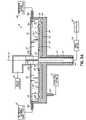
- the process chamber 16includes a first wall 32 , a second wall 34 , and a peripheral sidewall 36 that extends between and connects the first and second walls 32 , 34 to define the boundaries of a processing space 38 .
- the second wall 34is spaced apart from the first side wall 32 by the height or vertical dimension, d, of the peripheral sidewall 36 and is oriented generally parallel to the first wall 32 .
- the peripheral sidewall 36extends circumferentially about an azimuthal axis 40 of symmetry. The diameter of the peripheral sidewall 36 is significantly larger than the vertical dimension, d, so that the process chamber 16 has a flat “pancake” geometrical shape.
- a fore line 42which has the form of a duct or tubular conduit bent at a right angle, is coupled with a port 44 extending through the first wall 32 of the process chamber 16 .
- the fore line 42couples the processing space 38 in fluid communication with a vacuum system 46 , which consists of conventional vacuum pumps of a type used to evacuate gases from an enclosed volume like processing space 38 .
- a vacuum system 46which consists of conventional vacuum pumps of a type used to evacuate gases from an enclosed volume like processing space 38 .
- the fore line 42is depicted as angled with a right angle bend, a person having ordinary skill in the art would appreciate that the fore line 42 may have any desired angular bend or may be straight with no bend at all. The latter configuration is believed to optimize the pumping conductance.
- a susceptor having the form of a substrate support 48is disposed inside the process chamber 16 .
- the substrate support 48includes a disk-shaped platter 50 and a plurality of circular pockets or recesses 52 defined in a top surface 49 of the platter 50 .
- the top surface 49 of the platter 50faces toward first wall 32 so that the recesses 52 open toward the first wall 32 .
- Each of the recesses 52is configured to hold at least one of the substrates 15 at a location radially within the peripheral sidewall 36 of the process chamber 16 .
- the number of individual recesses 52may range, for example, from 2 to 7.
- the substrate support 48may be configured with any desired number of recesses 52 depending on the dimensions of the substrates 15 and the dimensions of the substrate support 48 .
- configuring the platter 50 with between 3 and 6 recesses 52 shaped to receive round substrates 15may optimize the usable fraction of the surface area of top surface 49 .
- this embodiment of the inventionis depicted as having recesses 52 of a circular or round geometrical shape, one of ordinary skill in the art would appreciate that the recesses 52 may be of any desired shape to accommodate an appropriately shaped substrate.
- the deposition system 10may be configured to process 200 mm substrates, 300 mm substrates, or larger-sized round substrates, which dimensioning will be reflected in the dimensions of recesses 52 .
- the deposition system 10may be configured to process substrates, wafers, or liquid crystal displays regardless of their size, as would be appreciated by those skilled in the art. Therefore, while aspects of the invention will be described in connection with the processing of substrates 15 that are semiconductor substrates, the invention is not so limited.
- the recesses 52are distributed circumferentially on the platter 50 about a uniform radius centered on an axis of rotation 54 .
- the recesses 52have approximately equiangular spacing about the axis of rotation 54 , which is substantially collinear or coaxial with the azimuthal axis 40 although the invention is not so limited.
- adjacent recesses 52may be separated by a gap distance equal to s ⁇ 2 w r , wherein s is the distance between the centers of the adjacent recesses 52 , and w r is the radius of the adjacent recesses 52 .
- the fore line 42which provides for evacuation of the atmosphere of the processing space 38 , is disposed along the axis of rotation 54 and above the platter 50 .
- the platter 50 of the substrate support 48is coupled with a drive motor 56 , which is disposed outside of the process chamber 16 , by a drive shaft 58 .
- the drive shaft 58which extends along the axis of rotation 54 , is disposed in a tubular extension 35 of the second wall 34 .
- a rotary vacuum feedthrough 60couples the drive shaft 58 with the drive motor 56 .
- the rotary vacuum feedthrough 60is configured to transmit rotary motion from the drive motor 56 through the second wall 34 to the drive shaft 58 for rotating the platter 50 about the axis of rotation 54 .
- a controller 62which is electrically coupled to the drive motor 56 , operates the drive motor 56 to rotate the platter 50 and drive shaft 58 about the axis of rotation 54 .
- the rotation of the platter 50may be continuous and may occur at a constant angular velocity about the axis of rotation 54 .
- the angular velocitymay be varied contingent upon the angular orientation of the platter 50 relative to an arbitrary reference point.
- the portion of the processing space 38 between the platter 50 and the second wall 34includes a pedestal 64 and a heater 66 .
- the heater 66is coupled to the pedestal 64 such that the heater 66 is at an intermediate location between a bottom surface 51 of the platter 50 and an upper surface 65 of the pedestal 64 .
- the heater 66transfers heat energy to the platter 50 for heating the substrates 15 held within the plurality of recesses 52 to a desired processing temperature.
- Partitions 68 , 70 , 72 , 74compartmentalize the processing space 38 of process chamber 16 into a plurality of compartments 76 , 78 , 80 , 82 .
- the partitions 68 , 70 , 72 , 74extend radially relative to the axis of rotation 54 toward the peripheral sidewall 36 .
- the partitions 68 , 70 , 72 , 74project upwardly from the top surface 49 of platter 50 towards the first wall 32 .
- Each of the partitions 68 , 70 , 72 , 74has a height or vertical dimension, d 1 , approximately equal to the vertical dimension, d 2 , between the top surface 49 of platter 50 and the confronting surface of the first wall 32 .
- Partition 68extends between a first end 68 a near the peripheral sidewall 36 and a second end 68 b proximate to the axis of rotation 54 .
- Partitions 70 , 72 , 74have similar first and second ends 70 a,b, 72 a,b, and 74 a,b, respectively.
- the respective ends 68 b, 70 b, 72 b, 74 b of partitions 68 , 70 , 72 , 74intersect inside the fore line 42 at the axis of rotation 54 , which may further reduce gas exchange among the four compartments 76 , 78 , 80 , 82 .
- the intersecting ends 68 b, 70 b, 72 b, 74 bproject upwardly such that the vertical dimension, d 3 , of the partitions 68 , 70 , 72 , 74 is greater within the fore line 42 than the vertical dimension, d 1 , outside of the fore line 42 .
- the inventionis not so limited as the partitions 68 , 70 , 72 , 74 may have a uniform vertical dimension, d 1 , along their entire lengths.
- Compartment 76is defined as a portion of the processing space 38 bounded between the first partition 68 , the second partition 70 , the first wall 32 , the second wall 34 , and the peripheral sidewall 36 .
- Compartment 78is defined as a portion of the processing space 38 bounded between the second partition 70 , the third partition 72 , the first wall 32 , the second wall 34 , and the peripheral sidewall 36 .
- Compartment 80is defined as a portion of the processing space 38 bounded between the third partition 72 , the fourth partition 74 , the first wall 32 , the second wall 34 , and the peripheral sidewall 36 .
- Compartment 82is defined as a portion of the processing space 38 bounded between the first partition 68 , the fourth partition 74 , the first wall 32 , the second wall 34 , and the peripheral sidewall 36 .
- four partitions 68 , 70 , 72 , 74are representatively shown, a person having ordinary skill in the art would appreciate that the process chamber 16 may be subdivided with any suitable plurality of partitions to form more or less than four compartments.
- deposition system 10further includes a purge gas supply system 84 coupled by respective gas lines 85 , 87 , with inlet ports 86 , 88 penetrating through the peripheral sidewall 36 .
- Inlet port 86 and gas line 85couple compartment 78 with the purge gas supply system 84 .
- Inlet port 88 and gas line 87couple compartment 82 with the purge gas supply system 84 .
- the purge gas supply system 84is configured to introduce a flow of a purge gas to compartments 78 and 82 .
- the purge gas introduced into the compartments 78 and 82can comprise an inert gas, such as a noble gas (i.e., helium, neon, argon, xenon, krypton), or nitrogen, or hydrogen.
- a noble gasi.e., helium, neon, argon, xenon, krypton
- purge gasis continuously introduced into the compartments 78 and 82 to provide a gaseous curtain or barrier preventing, or at the least significantly limiting, transfer of first and second process materials between compartments 76 , 80 .
- the purge gasalso provides an inert atmosphere inside compartments 78 , 82 so that any process material layers carried by the substrates 15 are substantially unchanged when transported on the platter 50 through compartments 78 , 82 .
- Compartment 76is juxtaposed between compartments 78 , 82 and compartment 80 is juxtaposed between compartments 78 , 82 so that compartments 78 , 82 separate compartments 76 and 80 to
- Deposition system 10further includes a first process material supply system 90 configured to introduce a first process material to compartment 76 , and a second process material supply system 92 configured to introduce a second process material to compartment 80 .
- the first and second material supply systems 90 , 92may each include one or more material sources, one or more heaters, one or more pressure control devices, one or more flow control devices, one or more filters, one or more valves, or one or more flow sensors as conventionally found in such process material supply systems.
- the first process materialcan, for example, comprise a precursor, such as a composition having the principal atomic or molecular species found in a film formed on each of the substrates 15 .
- the precursorcan originate as a solid phase, a liquid phase, or a gaseous phase, and it may be delivered to compartment 76 in either a gaseous or vapor phase, and either with or without the assistance of a carrier gas.
- the second process materialcan, for example, comprises a reactant, which may also have atomic or molecular species found in the thin film formed on substrates 15 .
- the reactantcan originate as a solid phase, a liquid phase, or a gaseous phase, and it may be delivered to compartment 80 in either a gaseous or vapor phase, and either with or without the assistance of a carrier gas.
- the first process material supplied by the first process material supply system 90 to process chamber 16 and the second process material supplied by the second process material supply system 92 to process chamber 16are selected in accordance with the composition and characteristics of a material to be deposited as the thin film on the substrate.
- the first process materialcan include a metal organic precursor, such as trimethylaluminum (TMA), and the second process material can include nitrogen (N 2 ) or oxygen (O 2 ).
- the first process materialcan include a precursor, such as tantalum pentachloride (TaCl 5 ), and the second process material can include a reducing agent, such as hydrogen (H 2 ) gas.
- TMAtrimethylaluminum
- the first process materialcan include a precursor, such as tantalum pentachloride (TaCl 5 )
- the second process materialcan include a reducing agent, such as hydrogen (H 2 ) gas.
- the temperature and pressure of the first and second process materialsare also selected to promote thin film growth.
- a first set of injection ports 102 and a second set of injection ports 104extend through the peripheral sidewall 36 to communicate with compartment 76 .
- the injection ports 102 , 104which collectively define a material injector 100 , are coupled by a first manifold 94 with the first process material supply system 90 .
- Injection ports 102 , 104inject the first process material into the compartment 76 .
- a third set of injection ports 108 and a fourth set of injection ports 110extend through the peripheral sidewall 36 to communicate with compartment 80 .
- the injection ports 108 , 110which collectively define a material injector 106 , are coupled by a second manifold 96 with the second process material supply system 92 .
- Injection ports 108 , 110inject the second process material into the compartment 80 .
- Injection ports 102 of material injector 100are located proximate to the first partition 68 . Injection ports 102 are aligned along a first angular arc 112 extending about the peripheral sidewall 36 in a first plane 114 ( FIG. 3A ). The first plane 114 is located above the second set of injection ports 104 and at a height, hi, above the top surface 49 of the platter 50 . The first plane 114 is substantially parallel to a plane containing the top surface 49 . Injection ports 104 of material injector 100 are located proximate to the second partition 70 . Injection ports 104 are aligned along a second angular arc 116 extending about the peripheral sidewall 36 in a second plane 118 . The second plane 118 is located at a height, h 2 , above the top surface 49 of the platter 50 and is substantially parallel to the plane containing the top surface 49 .
- Injection ports 108 of material injector 106is spatially positioned proximate to the third partition 72 .
- Injection ports 108are aligned along a third angular arc 120 extending about the peripheral sidewall 36 in a third plane 122 .
- the third plane 122is located above the second set of injection ports 110 and at a height, h 3 , above the top surface 49 of the platter 50 .
- the third plane 122is substantially parallel to the plane containing the top surface 49 .
- Injection ports 110are spatially positioned proximate to the fourth partition 74 .
- Injection ports 110are disposed along a fourth angular arc 124 extending about the peripheral sidewall 36 in a fourth plane 126 .
- the fourth plane 126is at a height, h 4 , above the top surface 49 of the platter 50 and is parallel to the plane containing the top surface 49 .
- the angular arcs 112 , 116 , 120 , 124are each measured circumferentially about the peripheral sidewall 36 .
- the first set of injection ports 102 and the third set of injection ports 108are substantially coplanar, so that height, h 1 , and height, h 3 , are substantially equal, and the second set of injection ports 104 and the fourth set of injection ports 110 are substantially coplanar, so that height, h 2 , and height, h 4 , are substantially equal.
- the heights h 1 -h 4may be adjusted such that planes 114 , 118 , 122 , 126 may have other relative arrangements, as would be appreciated by a person having ordinary skill in the art.
- the first angular arc 112 and the third angular arc 120may each span an arc angle of about 44°.
- the second angular arc 116 and the fourth angular arc 124may each span an arc angle of about 22°.
- each of the compartments 76 , 78 , 80 , 82may be independently equipped with any desired number of injection ports 102 , 104 , 108 , 110 , respectively, and that the respective angular arcs 112 , 116 , 120 , 124 may each span any desired arc angle.
- the number of injection ports 102 , 104 , 108 , 110 and the arc angles for the angular arcs 112 , 116 , 120 , 124are selected to cooperate for optimizing at least one property of the thin film being deposited on each of the substrates 15 and/or for optimizing the flow of the first and second process materials across the top surface of the substrates 15 .
- the material injectors 100 , 106may be configured to inject the respective first and second process materials in a substantially radial direction away from the peripheral sidewall 36 and toward the axis of rotation 54 .
- process material injection from each of the material injectors 100 , 106 in combination with simultaneous evacuation through the fore line 42creates a gas flow of the respective process materials from the peripheral sidewall 36 , across the substrates 15 in a direction substantially parallel to the top surface of each of the substrates 15 , and towards the central location of fore line 42 .
- excess process materials and deposition by-products from reactions transpiring at the top surface of the substrates 15are removed through the fore line 42 as fresh process materials are replenished in the compartments 76 , 80 .
- each substrate 15is serially exposed to first process material in the environment inside the first compartment 76 , then to the purge gas comprising the environment inside the second compartment 78 , then to the second process material in the environment inside the third compartment 80 , and finally to the purge gas comprising the environment inside the fourth compartment 82 .
- Each of the recesses 52has a desired dwell time in each of the respective compartments 76 , 78 , 80 , 82 , as mandated by the characteristics of the thin film to be deposited on each of the substrates 15 , sufficient to form the thin film.
- the second wall 34includes a bottom purge opening 130 for introducing a purge gas from a purge gas system 131 into the process chamber 16 beneath or under the substrate support 48 .
- the presence of purge gas under the substrate support 48may serve to reduce the transfer of the first and second process materials outside of their respective compartments 76 , 80 .
- the process chamber 16 of the deposition system 10is used for depositing a layer on each of the substrates 15 received in the recesses 52 on the platter 50 and arranged with a spaced circumferential relationship about the axis of rotation 54 .
- the substrates 15are continuously rotated in a closed path about the axis of rotation 54 , as indicated by the single-headed arrow 89 ( FIGS. 1 , 2 , 2 A).
- the angular velocitymay be, for example, about 240 revolutions per minute.
- a first process materialis injected in a radial direction relative to the axis of rotation 54 and into the first compartment 76 , which bounds the first angular arc 112 about the axis of rotation 54 .
- Each of the continuously rotating substrates 15is exposed to the first process material within the first compartment 76 during each complete rotation of the platter 50 .
- the first process materialis injected in a first stream at the first height, h 1 , above the substrates 15 over the first angular arc 112 within the first compartment 76 and in a second stream at the second height, h 2 , above the substrates 15 over the second angular arc 116 within the first compartment 76 .
- each of the continuously rotating substratesis exposed to an inert atmosphere within the second and fourth compartments 78 , 82 , which respectively bound the second and fourth angular arcs 116 , 126 about the axis of rotation 54 during each complete rotation.
- the second process materialis injected in the radial direction relative to the axis of rotation 54 and into the third compartment 80 , which is isolated from the first compartment 76 by the second and fourth compartments 78 , 82 .
- the layeris incrementally formed as a series of discrete thin film lamina on each of the continuously rotating substrates 15 by chemical reactions of the first and second process materials.
- the vacuum pressures inside the first and second compartments 76 , 80may be on the order of 10 Torr and the substrates 15 may be heated to a process temperature of about 400° C. while exposed to the first and second process materials.
- the deposition process formis a conventional deposition technique in which deposition of each atomic layer of the thin film, or a fraction thereof, on the substrates 15 is controlled by alternating and sequential introduction of appropriate gas phase precursors that react in a self-limiting manner to incrementally form or build the thin film.
- molecules of the first process materialbond (chemically, by absorption, by adsorption, etc.) to the top surface of each of the substrates 15 to form a monolayer or a fraction of a monolayer of the first process material.
- the second process materialreacts with the molecules of the first process material on each successive substrate 15 .
- first and third compartments 76 , 80As the substrates 15 are rotated through the first and third compartments 76 , 80 , these steps are repeated with sequential subsequent exposures to the first and second process materials.
- the environments of first and second process materials in the first and third compartments 76 , 80are isolated from each other by the chemically non-reactive, purge gas environments inside the second and fourth compartments 78 , 82 .
- the environments inside the first and third compartments 76 , 80are not altered to achieve the successive exposure to the first and second materials.
- the substrates 15may be heated to a process temperature to promote the deposition process.
- ALDis predominantly chemically driven. Accordingly, ALD may be conducted at significantly lower substrate temperatures than CVD.
- the rotation of the substrates 15may be regulated such that different substrates 15 are exposed to the first process material when the injection of the first process material is initiated and the injection of the first process material is discontinued. This type of regulation may be effective for controlling the uniformity of deposited layers that are relatively thin.
- the compartments 76 , 78 , 80 , 82may be evacuated through the fore line 42 communicating with the first compartment from a location above the substrates.
- the substrates 15may be rotated about the axis of rotation 54 with a constant angular velocity.
- the partitions 68 , 70 , 72 , 74 compartmentalizing the processing space 38may be adjusted such that the compartments 76 , 78 , 80 , 82 are merged together into a single compartment for depositing layers by CVD processes in the process chamber 16 .
- the partitions 68 , 70 , 72 , 74may be configured to be pivoted, as indicated by reference numeral 135 , by a positioning device (not shown) about a radial axis 137 extending generally from the axis of rotation 54 from a vertical orientation (as shown in FIGS. 1 , 2 , 2 A, 3 A, 3 B) to a substantially horizontal orientation.
- Gas injected through the material injectors 100 , 106may be used to deliver the first and second process materials for the CVD deposition process.
- the CVD deposition processmay be conducted with the substrate support 48 rotating or, alternatively, with the substrate support 48 stationary.
- a process chamber 16 aincludes a material injector 100 a that substitutes slotted injection ports 136 , 138 for the respective sets of injection ports 102 , 104 ( FIGS. 2 , 2 A, 3 A, 3 B), and a material injector 106 a that substitutes slotted injection ports 140 , 142 for the respective sets of injection ports 108 , 110 ( FIGS. 2 , 2 A, 3 A, 3 B).
- injection slot 136is spatially positioned proximate to the first partition 68 and is aligned along the first angular arc 112 .
- injection slot 138is spatially positioned proximate to the second partition 70 and is aligned along the second angular arc 116 .
- injection slot 140is spatially positioned proximate to the third partition 72 and is aligned along the third angular arc 120 .
- injection slot 142is spatially positioned proximate to the fourth partition 74 and is disposed along the fourth angular arc 124 .
- the properties of the injections slots 136 , 138 , 140 , 142are substantially similar to the properties of the injection ports 102 , 104 , 108 , 110 , as described hereinabove.
- a process chamber 16 bincludes a fore line 42 a, which has the form of a duct or tubular conduit bent at a right angle, coupled with a port 44 a extending through the second wall 34 of the process chamber 16 b.
- a fore line 42 awhich has the form of a duct or tubular conduit bent at a right angle, coupled with a port 44 a extending through the second wall 34 of the process chamber 16 b.
- the first and second angular arcs 112 , 116overlap such that at least one of the injection ports 102 overlaps spatially with at least one of the injection ports 104 but in different planes 114 , 118 .
- the third and fourth angular arcs 120 , 124overlap such that at least one of the injection ports 108 overlaps spatially with at least one of the injection ports 110 but in different planes 122 , 126 .
- a process chamber 16 cincludes a material injector 100 b that includes a plasma source 144 that supplies the first process material to compartment 76 in the form of a plasma product comprising ions, radicals, or a combination thereof.
- Waveguides 146 a,bcouple the plasma source 144 with injection ports 148 , 150 in the peripheral sidewall 36 of the process chamber 16 c.
- Injection port 148is located proximate to the first partition 68 and the second injection port 150 is located proximate to the second partition 70 .
- Process chamber 16 cfurther includes a material injector 106 b that includes a plasma source 152 that supplies the second process material to compartment 80 in the form of a plasma product comprising ions, radicals, or a combination thereof.
- Waveguides 154 a,bcouple the plasma source 152 with injection ports 156 , 158 in the peripheral sidewall 36 of the process chamber 16 .
- Injection port 156is located proximate the third partition 72 and injection port 158 is located proximate the fourth partition 74 .
- the process chamber 16 cmay be used for plasma-enhanced atomic layer deposition of thin films on the substrates 15 .
- the inventioncontemplates that, although process chamber 16 c includes multiple plasma sources 144 , 152 , either the first process material or the second process material may be supplied to compartments 76 , 80 using injection ports 102 , 104 , 108 , 110 ( FIGS. 1 , 2 , 2 A, 3 A, 3 B) or slotted injection ports 136 , 138 , 140 , 142 ( FIG. 4 ).
- the location of the injection ports 148 , 150 about the sidewall 36may be used to modulate the uniformity of the deposited film on substrates 15 .
- the angular orientation of the partitions 68 , 70 , 72 , 74may be adjusted to change the arc lengths of angular segments occupied by the compartments 76 , 78 , 80 , 82 .
- the partitions 68 , 70 , 72 , 74are arranged relative to each other with included right angles that are congruent. As the platter 50 of substrate support 48 ( FIG. 2 ) is rotated with a constant angular velocity, the substrates 15 carried by the platter 50 are exposed sequentially to each compartment 76 , 80 for about approximately equivalent dwell times to form repeating layers of the first and second process materials on the top surface of each of the substrates 15 .
- This arrangement for partitions 68 , 70 , 72 , 74is representative of process chambers 16 , 16 a, 16 b, 16 a depicted in FIGS. 1-6 .
- the processing space 38is divided into compartments 76 a, 78 a, 80 a, 82 a, which are similar to compartments 76 , 78 , 80 , 82 , by partitions 68 a, 70 a, 72 a, 74 a, which are similar to partitions 68 , 70 , 72 , 74 .
- the first and second partitions 68 a, 70 aare separated by an obtuse included angle and bound compartment 76 a.
- the third and fourth partitions 72 a, 74 aare separated by an obtuse included angle and bound compartment 80 a.
- the obtuse included angle between the third and fourth partitions 72 a, 74 ais congruent with the obtuse included angle between the first and second partitions 68 a, 70 a because these obtuse included angles represent vertical angles.
- the obtuse included angles between the first and second partitions 68 a, 70 a and between the third and fourth partitions 72 a, 74 anecessarily create equivalent acute angles between the second and third partitions 70 a, 72 a and between the first and fourth partitions 68 a, 74 a.
- the acute angle between the second and third partitions 70 a, 72 a, which bound compartment 78 a,is congruent with the acute angle between the first and fourth partitions 68 a, 74 a, which bound compartment 82 a.
- These congruent acute included anglesrepresent vertical angles.
- the acute included angle between the second and third partitions 70 a, 72 a and the obtuse included angle either between the third and fourth partitions 72 a, 74 a or between the first and second partitions 68 a, 70 aare supplemental angles.
- the acute included angle between the first and fourth partitions 68 a, 74 a and the obtuse included angle either between the third and fourth partitions 72 a, 74 a or between the first and second partitions 68 a, 70 aare also supplemental angles.
- the substrates 15 carried by the platter 50are exposed sequentially to the first and second process materials with larger dwell times than for the arrangement shown in FIG. 7 , assuming equal angular velocities.
- the dwell times in the first and third compartments 76 a, 80 aare approximately equal.
- the angles between the partitions 68 a, 70 a, 72 a, 74 a and angular velocitycan be adjusted to adjust the dwell time of the substrates 15 in each of the compartments 76 a, 80 a.
- the increase exposure to the first and second process materialsmay operate to increase the growth rate for the thin film.
- the processing space 38is divided into compartments 76 b, 78 b, 80 b, 82 b, which are similar to compartments 76 , 78 , 80 , 82 , by partitions 68 b, 70 b, 72 b, 74 b, which are similar to partitions 68 , 70 , 72 , 74 .
- the included angle, ⁇ 1between the first and second partitions 68 b, 70 b is greater than the included angle, ⁇ 2 , between the third and fourth partitions 72 b, 74 b.
- the included angle, ⁇ 3between the second and third partitions 70 b, 72 b is approximately equal to the included angle, ⁇ 4 , between the first and fourth partitions 68 b, 74 b.
- the substrates 15 carried by the platter 50are sequentially exposed to the first process material in the first compartment 76 b for a first dwell time, to purge gas in the second compartment 78 b for a second dwell time wherein the second dwell time is shorter than the first dwell time, to the second process material in the third compartment 80 b for a third dwell time wherein the third dwell time is shorter than the first dwell time, and again to purge gas in the fourth compartment 82 b for a dwell time equivalent to the second dwell time, thereby forming repeating layers of the first and second process materials on the top surface of each of the substrates 15 .
- the individual dwell timesare independent of the angular velocity if the platter 50 of substrate support 48 ( FIG. 2 ) is rotated at a constant angular velocity.
- partitions 68 b, 70 b, 72 b, 74 bare arranged such that ⁇ 1 is about 270° and ⁇ 2 is about 30°, a person having ordinary skill in the art would appreciate that the partitions 68 b, 70 b, 72 b, 74 b can be configured to provide for any desired dwell times within the four compartments 76 b, 78 b, 80 b, 82 b. The dwell times may be adjusted to, for example, compensate for first and second process materials having different reaction rates.
- the dwell time for exposure to the first process material in the first compartment 76 bis significantly greater than the dwell time for exposure to the second process material in the second compartment 80 b, which would maximize the exposure to the first process material to compensate for a second process material that is fast acting.
Landscapes
- Chemical & Material Sciences (AREA)
- Engineering & Computer Science (AREA)
- General Chemical & Material Sciences (AREA)
- Chemical Kinetics & Catalysis (AREA)
- Materials Engineering (AREA)
- Mechanical Engineering (AREA)
- Metallurgy (AREA)
- Organic Chemistry (AREA)
- Physics & Mathematics (AREA)
- Condensed Matter Physics & Semiconductors (AREA)
- General Physics & Mathematics (AREA)
- Manufacturing & Machinery (AREA)
- Computer Hardware Design (AREA)
- Microelectronics & Electronic Packaging (AREA)
- Power Engineering (AREA)
- Electromagnetism (AREA)
- Plasma & Fusion (AREA)
- Chemical Vapour Deposition (AREA)
- Crystals, And After-Treatments Of Crystals (AREA)
Abstract
Description
- This invention relates to systems and methods for depositing thin films using Atomic Layer Deposition (ALD).
- As dimensions for microelectronics are reduced and the demand for such materials increase, thin semiconductor films having uniform composition and uniform thickness over a larger substrate area are increasingly desirable. A common process used for depositing thin films on a substrate is Chemical Vapor Deposition (CVD), which provides for deposition of relatively uniform films over complex device topography. In a typical CVD process, the substrate is exposed to two or more volatile precursors, which react and/or decompose on the substrate surface to produce the desired thin film.
- Despite improvements of CVD over previous deposition techniques, CVD has several disadvantages. For example, because CVD is flux-dependent, deposition conditions such as substrate temperature, pressure, and gas flow rate must be accurately and consistently maintained to produce a desired thin film of uniform thickness. Additionally, CVD tends to incorporate undesired reaction products into the deposited thin film, thereby diminishing the purity of the thin film.
- Atomic Layer Deposition (ALD), which represents a variant of CVD, is a contemporary technology for depositing thin films now emerging as a potentially superior method of achieving highly uniform, conformal film deposition. ALD is a process wherein conventional CVD processes are divided into separate deposition steps to construct the thin film by sequentially depositing single atomic monolayers in each deposition step. The technique of ALD is based on the principle of the formation of a saturated monolayer of reactive precursor molecules by chemisorption. A typical ALD process consists of injecting a first precursor for a period of time until a saturated monolayer is formed on the substrate. Then, the first precursor is purged from the chamber using an inert gas. This is followed by injecting a second precursor into the chamber, also for a period of time, thus forming a layer on the wafer from the reaction of the second precursor with the first precursor. Then, the second precursor is purged from the chamber. This process of introducing the first precursor, purging the process chamber, introducing the second precursor, and purging the process chamber is repeated a number of times to achieve a layer of a desired thickness.
- ALD thin films may be deposited using single wafer reactors with the reactive gas precursors injected into the process chamber horizontally. The horizontal gas precursor injection directs the gas precursors in a direction parallel to the surface of a stationary substrate. Arrangements in which the reactive gas precursors flow in a direction parallel to the substrate surface are desirable because they result in more uniform thin films than those deposited by gas precursors injected vertically in a direction perpendicular to the substrate surface. Nevertheless, a major disadvantage of a single wafer reactor is that it has a significantly diminished commercial value because of its relatively low throughput. Another disadvantage is that the process chamber must be purged before each individual gas precursor is introduced.
- At least in part to overcome the commercial problems associated with single wafer reactors, multi-wafer reactors may be used for ALD processes in which the process chamber is partitioned into a plurality of process compartments. The substrates are rotated relative to the process compartments such that each substrate is sequentially transferred from one compartment to another. In each individual process compartment, each substrate is exposed to either a precursor gas or an inert gas. The rotating substrates are sequentially exposed to the different precursor gases and the inert gas. One characteristic disadvantage of these multi-wafer reactors is that multi-wafer reactors employ showerhead injectors that inject the precursor gases in an axially symmetric direction generally perpendicular to the substrate surface. As a result, although faster process times are achieved, multi-wafer ALD process chambers may produce thin films with reduced thickness uniformity.
- Therefore, there is a need for a multi-wafer process chamber in which the reactive gas precursors are injected into each process compartment in a direction parallel to the top surface of the substrates.
- One embodiment of the invention provides a deposition system for processing a plurality of substrates. The deposition system comprises a process chamber including a first wall, a second wall spaced apart from the first wall, and a peripheral sidewall connecting the first and second walls to define a processing space. A substrate support is configured to support the substrates between the first and second walls and radially inside the peripheral sidewall. The substrate support is configured to rotate the substrates relative to the peripheral sidewall in a closed path about an axis of rotation. A plurality of partitions extend relative to the axis of rotation toward the peripheral sidewall. The partitions divide the processing space into a plurality of compartments including a first compartment and a second compartment containing an inert atmosphere. A first material injector communicates through the peripheral sidewall with the first compartment and is configured to inject a first process material into the first compartment. A top surface of each of the substrates, during each complete rotation about the axis of rotation, is sequentially exposed to the first process material in the first compartment and the inert atmosphere in the second compartment.
- Another embodiment of the invention provides a method for depositing a layer on each of a plurality of substrates. The method comprises arranging the substrates with a spaced circumferential relationship about an axis of rotation and rotating the substrates in a closed path about the axis of rotation. The method further comprises injecting a first process material in a radial direction relative to the axis of rotation and into a first compartment defined by partitions bounding a first included angle about the axis of rotation. During each complete rotation, a top surface of each of the substrates is exposed to the first process material within the first compartment to bond molecules of the first process material and, moreover, to an inert atmosphere within a second compartment defined by partitions bounding a second included angle about the axis of rotation.
- The accompanying drawings, which are incorporated in and constitute a part of this specification, illustrate embodiments of the invention and, together with a general description of the invention given above, and the detailed description given below, serve to explain the invention.
FIG. 1 is a diagrammatic top plan view of a deposition system including a process chamber in accordance with an embodiment of the invention.FIG. 2 is a perspective view of the process chamber ofFIG. 1 with a top wall omitted for clarity.FIG. 2A is a top view of the process chamber ofFIG. 2 .FIG. 3A is a schematic cross-sectional view taken generally alongline 3A-3A inFIG. 2 .FIG. 3B is a schematic cross-sectional view taken generally alongline 3B-3B inFIG. 2 .FIG. 4 is a perspective view similar toFIG. 2 of a process chamber in accordance with an alternative embodiment of the invention.FIG. 5 is a schematic cross-sectional view similar toFIG. 3A of a process chamber in accordance with an alternative embodiment of the invention.FIG. 6 is a perspective view similar toFIG. 2 of a process chamber in accordance with another alternative embodiment of the invention.FIGS. 7-9 are diagrammatic views showing arrangements of partitions for compartmentalizing a processing space inside the process chamber ofFIGS. 1 ,2,2A,3A, and3B in accordance with embodiments of the invention.- With reference to
FIG. 1 , adeposition system 10 for processing a plurality ofsubstrates 15 comprises an input/output station 12, a load/lock station 14, aprocess chamber 16, and atransfer chamber 18 interposed between the load/lock station 14 andprocess chamber 16. Thedeposition system 10, which is shown in a simplified manner, may include additional structures, such as additional vacuum-isolation walls coupling the load/lock station 14 with thetransfer chamber 18 and theprocess chamber 16 with thetransfer chamber 18, as understood by a person having ordinary skill in the art. The input/output station 12, which is at or near atmospheric pressure (e.g., 760 Torr), is adapted to receivewafer cassettes 20, such as front opening unified pods (FOUPs). Thewafer cassettes 20 are sized and shaped to hold a plurality ofsubstrates 15, such as semiconductor wafers having diameters of, for example, 200 or 300 millimeters. - The load/
lock station 14 is adapted to be evacuated from atmospheric pressure to a vacuum pressure and to be vented from vacuum pressure to atmospheric pressure, while theprocess chamber 16 andtransfer chamber 18 are isolated and maintained continuously under vacuum pressures. The load/lock station 14 holds a plurality of thewafer cassettes 20 introduced from the atmospheric pressure environment of the input/output station 12. The load/lock station 14 includesplatforms wafer cassettes 20 and that can be vertically indexed to promote wafer transfers to and from theprocess chamber 16. - A
wafer transfer mechanism 22transfers substrates 15 under vacuum from one of thewafer cassettes 20 in the load/lock station 14 through thetransfer chamber 18 and into theprocess chamber 16. Anotherwafer transfer mechanism 24transfers substrates 15 processed in theprocess chamber 16 under vacuum from theprocess chamber 16 through thetransfer chamber 18 and to thewafer cassette 20. Thewafer transfer mechanisms deposition system 10, may be selective compliant articulated/assembly robot arm (SCARA) robots commonly used for pick-and-place operations. Thewafer transfer mechanisms substrates 15 during transfers. Theprocess chamber 16 may include distinct first and second sealable ports (not shown) used bywafer transfer mechanisms FIGS. 3A ,3B) inside theprocess chamber 16. The access ports are sealed when a deposition process is occurring in theprocess chamber 16.Wafer transfer mechanism 22 is depicted inFIG. 1 as transferringunprocessed substrates 15 fromwafer cassette 20 onplatform 21 of the load/lock station 14 to theprocess chamber 16.Wafer transfer mechanism 24 is depicted inFIG. 1 as transferring processedsubstrates 15 from theprocess chamber 16 towafer cassette 20 onplatform 23 of the load/lock station 14. - The
wafer transfer mechanism 24 may also transfer processedsubstrates 15 extracted from theprocess chamber 16 to ametrology station 26 for examination or to a cool downstation 28 used for post-processing low pressure cooling of thesubstrates 15. The processes performed in themetrology station 26 may include, but are not limited to, conventional techniques used to measure film thickness and/or film composition, such as ellipsometry, and particle measurement techniques for contamination control. - The
deposition system 10 is equipped with asystem controller 30 programmed to control and orchestrate the operation of thedeposition system 10. Thesystem controller 30 typically includes a central processing unit (CPU) for controlling various system functions, chamber processes and support hardware (e.g., detectors, robots, motors, gas sources hardware, etc.) and monitoring the system and chamber processes (e.g., chamber temperature, process sequence throughput, chamber process time, input/output signals, etc.). Software instructions and data can be coded and stored within the memory for instructing the CPU. A software program executable by thesystem controller 30 determines which tasks are executed onsubstrates 15 including tasks relating to monitoring and execution of the processing sequence tasks and various chamber process recipe steps. - With continued reference to
FIGS. 2 ,2A,3A, and3B, theprocess chamber 16 includes afirst wall 32, asecond wall 34, and aperipheral sidewall 36 that extends between and connects the first andsecond walls processing space 38. Thesecond wall 34 is spaced apart from thefirst side wall 32 by the height or vertical dimension, d, of theperipheral sidewall 36 and is oriented generally parallel to thefirst wall 32. Theperipheral sidewall 36 extends circumferentially about anazimuthal axis 40 of symmetry. The diameter of theperipheral sidewall 36 is significantly larger than the vertical dimension, d, so that theprocess chamber 16 has a flat “pancake” geometrical shape. - A
fore line 42, which has the form of a duct or tubular conduit bent at a right angle, is coupled with aport 44 extending through thefirst wall 32 of theprocess chamber 16. Thefore line 42 couples theprocessing space 38 in fluid communication with avacuum system 46, which consists of conventional vacuum pumps of a type used to evacuate gases from an enclosed volume like processingspace 38. Although thefore line 42 is depicted as angled with a right angle bend, a person having ordinary skill in the art would appreciate that thefore line 42 may have any desired angular bend or may be straight with no bend at all. The latter configuration is believed to optimize the pumping conductance. - A susceptor having the form of a
substrate support 48 is disposed inside theprocess chamber 16. Thesubstrate support 48 includes a disk-shapedplatter 50 and a plurality of circular pockets or recesses52 defined in atop surface 49 of theplatter 50. Thetop surface 49 of theplatter 50 faces towardfirst wall 32 so that therecesses 52 open toward thefirst wall 32. - Each of the
recesses 52 is configured to hold at least one of thesubstrates 15 at a location radially within theperipheral sidewall 36 of theprocess chamber 16. The number ofindividual recesses 52 may range, for example, from 2 to 7. However, a person having ordinary skill in the art would appreciate that thesubstrate support 48 may be configured with any desired number ofrecesses 52 depending on the dimensions of thesubstrates 15 and the dimensions of thesubstrate support 48. For example, configuring theplatter 50 with between 3 and 6recesses 52 shaped to receiveround substrates 15 may optimize the usable fraction of the surface area oftop surface 49. Additionally, although this embodiment of the invention is depicted as havingrecesses 52 of a circular or round geometrical shape, one of ordinary skill in the art would appreciate that therecesses 52 may be of any desired shape to accommodate an appropriately shaped substrate. - The
deposition system 10 may be configured to process 200 mm substrates, 300 mm substrates, or larger-sized round substrates, which dimensioning will be reflected in the dimensions ofrecesses 52. In fact, it is contemplated that thedeposition system 10 may be configured to process substrates, wafers, or liquid crystal displays regardless of their size, as would be appreciated by those skilled in the art. Therefore, while aspects of the invention will be described in connection with the processing ofsubstrates 15 that are semiconductor substrates, the invention is not so limited. - The
recesses 52 are distributed circumferentially on theplatter 50 about a uniform radius centered on an axis of rotation54. Therecesses 52 have approximately equiangular spacing about the axis of rotation54, which is substantially collinear or coaxial with theazimuthal axis 40 although the invention is not so limited. As best shown inFIG. 2A ,adjacent recesses 52 may be separated by a gap distance equal to s−2 wr, wherein s is the distance between the centers of theadjacent recesses 52, and wris the radius of the adjacent recesses52. Thefore line 42, which provides for evacuation of the atmosphere of theprocessing space 38, is disposed along the axis of rotation54 and above theplatter 50. - With continued reference to
FIGS. 2 ,2A,3A, and3B, theplatter 50 of thesubstrate support 48 is coupled with adrive motor 56, which is disposed outside of theprocess chamber 16, by adrive shaft 58. Thedrive shaft 58, which extends along the axis of rotation54, is disposed in atubular extension 35 of thesecond wall 34. A rotary vacuum feedthrough60 couples thedrive shaft 58 with thedrive motor 56. Therotary vacuum feedthrough 60 is configured to transmit rotary motion from thedrive motor 56 through thesecond wall 34 to thedrive shaft 58 for rotating theplatter 50 about the axis of rotation54. - A
controller 62, which is electrically coupled to thedrive motor 56, operates thedrive motor 56 to rotate theplatter 50 and driveshaft 58 about the axis of rotation54. When thesubstrates 15 are processed in theprocess chamber 16, the rotation of theplatter 50 may be continuous and may occur at a constant angular velocity about the axis of rotation54. Alternatively, the angular velocity may be varied contingent upon the angular orientation of theplatter 50 relative to an arbitrary reference point. - The portion of the
processing space 38 between theplatter 50 and thesecond wall 34 includes apedestal 64 and aheater 66. Theheater 66 is coupled to thepedestal 64 such that theheater 66 is at an intermediate location between abottom surface 51 of theplatter 50 and anupper surface 65 of thepedestal 64. When powered, theheater 66 transfers heat energy to theplatter 50 for heating thesubstrates 15 held within the plurality ofrecesses 52 to a desired processing temperature. Partitions processing space 38 ofprocess chamber 16 into a plurality ofcompartments partitions peripheral sidewall 36. Thepartitions top surface 49 ofplatter 50 towards thefirst wall 32. Each of thepartitions top surface 49 ofplatter 50 and the confronting surface of thefirst wall 32.Partition 68 extends between afirst end 68anear theperipheral sidewall 36 and asecond end 68bproximate to the axis of rotation54.Partitions - The respective ends68b,70b,72b,74bof
partitions fore line 42 at the axis of rotation54, which may further reduce gas exchange among the fourcompartments partitions fore line 42 than the vertical dimension, d1, outside of thefore line 42. However, the invention is not so limited as thepartitions Compartment 76 is defined as a portion of theprocessing space 38 bounded between thefirst partition 68, thesecond partition 70, thefirst wall 32, thesecond wall 34, and theperipheral sidewall 36.Compartment 78 is defined as a portion of theprocessing space 38 bounded between thesecond partition 70, thethird partition 72, thefirst wall 32, thesecond wall 34, and theperipheral sidewall 36.Compartment 80 is defined as a portion of theprocessing space 38 bounded between thethird partition 72, thefourth partition 74, thefirst wall 32, thesecond wall 34, and theperipheral sidewall 36.Compartment 82 is defined as a portion of theprocessing space 38 bounded between thefirst partition 68, thefourth partition 74, thefirst wall 32, thesecond wall 34, and theperipheral sidewall 36. Although fourpartitions process chamber 16 may be subdivided with any suitable plurality of partitions to form more or less than four compartments.- With continued reference to
FIGS. 2 ,2A,3A, and3B and particularlyFIG. 2A ,deposition system 10 further includes a purgegas supply system 84 coupled byrespective gas lines inlet ports peripheral sidewall 36.Inlet port 86 andgas line 85couple compartment 78 with the purgegas supply system 84.Inlet port 88 andgas line 87couple compartment 82 with the purgegas supply system 84. The purgegas supply system 84 is configured to introduce a flow of a purge gas tocompartments compartments compartments compartments substrates 15 are substantially unchanged when transported on theplatter 50 throughcompartments Compartment 76 is juxtaposed betweencompartments compartment 80 is juxtaposed betweencompartments compartments separate compartments Deposition system 10 further includes a first processmaterial supply system 90 configured to introduce a first process material tocompartment 76, and a second processmaterial supply system 92 configured to introduce a second process material tocompartment 80. The first and secondmaterial supply systems - The first process material can, for example, comprise a precursor, such as a composition having the principal atomic or molecular species found in a film formed on each of the
substrates 15. For example, the precursor can originate as a solid phase, a liquid phase, or a gaseous phase, and it may be delivered tocompartment 76 in either a gaseous or vapor phase, and either with or without the assistance of a carrier gas. The second process material can, for example, comprises a reactant, which may also have atomic or molecular species found in the thin film formed onsubstrates 15. For instance, the reactant can originate as a solid phase, a liquid phase, or a gaseous phase, and it may be delivered tocompartment 80 in either a gaseous or vapor phase, and either with or without the assistance of a carrier gas. - The first process material supplied by the first process
material supply system 90 to processchamber 16 and the second process material supplied by the second processmaterial supply system 92 to processchamber 16 are selected in accordance with the composition and characteristics of a material to be deposited as the thin film on the substrate. For example, the first process material can include a metal organic precursor, such as trimethylaluminum (TMA), and the second process material can include nitrogen (N2) or oxygen (O2). In another example, the first process material can include a precursor, such as tantalum pentachloride (TaCl5), and the second process material can include a reducing agent, such as hydrogen (H2) gas. The temperature and pressure of the first and second process materials are also selected to promote thin film growth. - A first set of
injection ports 102 and a second set ofinjection ports 104 extend through theperipheral sidewall 36 to communicate withcompartment 76. Theinjection ports material injector 100, are coupled by afirst manifold 94 with the first processmaterial supply system 90.Injection ports compartment 76. A third set ofinjection ports 108 and a fourth set ofinjection ports 110 extend through theperipheral sidewall 36 to communicate withcompartment 80. Theinjection ports material injector 106, are coupled by asecond manifold 96 with the second processmaterial supply system 92.Injection ports compartment 80. Injection ports 102 ofmaterial injector 100 are located proximate to thefirst partition 68.Injection ports 102 are aligned along a firstangular arc 112 extending about theperipheral sidewall 36 in a first plane114 (FIG. 3A ). Thefirst plane 114 is located above the second set ofinjection ports 104 and at a height, hi, above thetop surface 49 of theplatter 50. Thefirst plane 114 is substantially parallel to a plane containing thetop surface 49.Injection ports 104 ofmaterial injector 100 are located proximate to thesecond partition 70.Injection ports 104 are aligned along a secondangular arc 116 extending about theperipheral sidewall 36 in asecond plane 118. Thesecond plane 118 is located at a height, h2, above thetop surface 49 of theplatter 50 and is substantially parallel to the plane containing thetop surface 49.Injection ports 108 ofmaterial injector 106 is spatially positioned proximate to thethird partition 72.Injection ports 108 are aligned along a thirdangular arc 120 extending about theperipheral sidewall 36 in athird plane 122. Thethird plane 122 is located above the second set ofinjection ports 110 and at a height, h3, above thetop surface 49 of theplatter 50. Thethird plane 122 is substantially parallel to the plane containing thetop surface 49.Injection ports 110 are spatially positioned proximate to thefourth partition 74.Injection ports 110 are disposed along a fourthangular arc 124 extending about theperipheral sidewall 36 in afourth plane 126. Thefourth plane 126 is at a height, h4, above thetop surface 49 of theplatter 50 and is parallel to the plane containing thetop surface 49. The angular arcs112,116,120,124 are each measured circumferentially about theperipheral sidewall 36.- In one embodiment of the invention, the first set of
injection ports 102 and the third set ofinjection ports 108 are substantially coplanar, so that height, h1, and height, h3, are substantially equal, and the second set ofinjection ports 104 and the fourth set ofinjection ports 110 are substantially coplanar, so that height, h2, and height, h4, are substantially equal. The heights h1-h4may be adjusted such thatplanes - In one specific embodiment of the invention, the first
angular arc 112 and the thirdangular arc 120 may each span an arc angle of about 44°. The secondangular arc 116 and the fourthangular arc 124 may each span an arc angle of about 22°. A person of ordinary skill in the art would appreciate that each of thecompartments injection ports angular arcs injection ports angular arcs substrates 15 and/or for optimizing the flow of the first and second process materials across the top surface of thesubstrates 15. - The
material injectors peripheral sidewall 36 and toward the axis of rotation54. In this configuration, process material injection from each of thematerial injectors fore line 42 creates a gas flow of the respective process materials from theperipheral sidewall 36, across thesubstrates 15 in a direction substantially parallel to the top surface of each of thesubstrates 15, and towards the central location offore line 42. As a consequence, excess process materials and deposition by-products from reactions transpiring at the top surface of thesubstrates 15 are removed through thefore line 42 as fresh process materials are replenished in thecompartments - When the
substrate support 48 is rotated about the axis of rotation54, the arrangement of therecesses 52 about the circumference of theplatter 50 allows eachsubstrate 15 to be sequentially exposed to the different environment inside each of thecompartments substrate support 48 through a closed path of27π radians (360°), each of thesubstrates 15 is serially exposed to first process material in the environment inside thefirst compartment 76, then to the purge gas comprising the environment inside thesecond compartment 78, then to the second process material in the environment inside thethird compartment 80, and finally to the purge gas comprising the environment inside thefourth compartment 82. Each of therecesses 52 has a desired dwell time in each of therespective compartments substrates 15, sufficient to form the thin film. - The
second wall 34 includes a bottom purge opening130 for introducing a purge gas from apurge gas system 131 into theprocess chamber 16 beneath or under thesubstrate support 48. The presence of purge gas under thesubstrate support 48 may serve to reduce the transfer of the first and second process materials outside of theirrespective compartments - In use and with reference to
FIGS. 1 ,2,2A,3A, and3B, theprocess chamber 16 of thedeposition system 10 is used for depositing a layer on each of thesubstrates 15 received in therecesses 52 on theplatter 50 and arranged with a spaced circumferential relationship about the axis of rotation54. Thesubstrates 15 are continuously rotated in a closed path about the axis of rotation54, as indicated by the single-headed arrow89 (FIGS. 1 ,2,2A). The angular velocity may be, for example, about 240 revolutions per minute. A first process material is injected in a radial direction relative to the axis of rotation54 and into thefirst compartment 76, which bounds the firstangular arc 112 about the axis of rotation54. Each of the continuously rotatingsubstrates 15 is exposed to the first process material within thefirst compartment 76 during each complete rotation of theplatter 50. The first process material is injected in a first stream at the first height, h1, above thesubstrates 15 over the firstangular arc 112 within thefirst compartment 76 and in a second stream at the second height, h2, above thesubstrates 15 over the secondangular arc 116 within thefirst compartment 76. - Before and after the exposure to the first process material, each of the continuously rotating substrates is exposed to an inert atmosphere within the second and
fourth compartments angular arcs third compartment 80, which is isolated from thefirst compartment 76 by the second andfourth compartments substrates 15 by chemical reactions of the first and second process materials. By way of example only and not limitation, the vacuum pressures inside the first andsecond compartments substrates 15 may be heated to a process temperature of about 400° C. while exposed to the first and second process materials. - The deposition process form is a conventional deposition technique in which deposition of each atomic layer of the thin film, or a fraction thereof, on the
substrates 15 is controlled by alternating and sequential introduction of appropriate gas phase precursors that react in a self-limiting manner to incrementally form or build the thin film. Within thefirst compartment 76, molecules of the first process material bond (chemically, by absorption, by adsorption, etc.) to the top surface of each of thesubstrates 15 to form a monolayer or a fraction of a monolayer of the first process material. Within thethird compartment 80, the second process material reacts with the molecules of the first process material on eachsuccessive substrate 15. As thesubstrates 15 are rotated through the first andthird compartments third compartments fourth compartments third compartments - The
substrates 15 may be heated to a process temperature to promote the deposition process. In comparison with predominantly thermally driven CVD processes, ALD is predominantly chemically driven. Accordingly, ALD may be conducted at significantly lower substrate temperatures than CVD. - The rotation of the
substrates 15 may be regulated such thatdifferent substrates 15 are exposed to the first process material when the injection of the first process material is initiated and the injection of the first process material is discontinued. This type of regulation may be effective for controlling the uniformity of deposited layers that are relatively thin. Thecompartments fore line 42 communicating with the first compartment from a location above the substrates. Thesubstrates 15 may be rotated about the axis of rotation54 with a constant angular velocity. - The invention contemplates that the
partitions processing space 38 may be adjusted such that thecompartments process chamber 16. Specifically, thepartitions reference numeral 135, by a positioning device (not shown) about aradial axis 137 extending generally from the axis of rotation54 from a vertical orientation (as shown inFIGS. 1 ,2,2A,3A,3B) to a substantially horizontal orientation. Gas injected through thematerial injectors substrate support 48 rotating or, alternatively, with thesubstrate support 48 stationary. - With reference to
FIG. 4 in which like reference numerals refer to like features inFIGS. 1 ,2,2A,3A, and3B and in accordance with an alternative embodiment of the invention, a process chamber16aincludes amaterial injector 100athat substitutes slottedinjection ports injection ports 102,104 (FIGS. 2 ,2A,3A,3B), and amaterial injector 106athat substitutes slottedinjection ports injection ports 108,110 (FIGS. 2 ,2A,3A,3B). Similar toinjection ports 102,injection slot 136 is spatially positioned proximate to thefirst partition 68 and is aligned along the firstangular arc 112. Similar toinjection ports 104,injection slot 138 is spatially positioned proximate to thesecond partition 70 and is aligned along the secondangular arc 116. Similar toinjection ports 108,injection slot 140 is spatially positioned proximate to thethird partition 72 and is aligned along the thirdangular arc 120. Similar toinjection ports 110,injection slot 142 is spatially positioned proximate to thefourth partition 74 and is disposed along the fourthangular arc 124. The properties of theinjections slots injection ports - With reference to
FIG. 5 in which like reference numerals refer to like features inFIGS. 1 ,2,2A,3A,3B, and4 and in accordance with an alternative embodiment of the invention, aprocess chamber 16bincludes afore line 42a,which has the form of a duct or tubular conduit bent at a right angle, coupled with a port44aextending through thesecond wall 34 of theprocess chamber 16b.In this bottom pumped configuration, excess process materials and deposition by-products are removed from theprocess chamber 16bthrough port44a.In this embodiment, the first and secondangular arcs injection ports 102 overlaps spatially with at least one of theinjection ports 104 but indifferent planes angular arcs injection ports 108 overlaps spatially with at least one of theinjection ports 110 but indifferent planes - With reference to
FIG. 6 in which like reference numerals refer to like features inFIGS. 1 ,2,2A,3A,3B,4 and5 and in accordance with an alternative embodiment of the invention, a process chamber16cincludes amaterial injector 100bthat includes aplasma source 144 that supplies the first process material tocompartment 76 in the form of a plasma product comprising ions, radicals, or a combination thereof. Waveguides146a,bcouple theplasma source 144 withinjection ports peripheral sidewall 36 of the process chamber16c.Injection port 148 is located proximate to thefirst partition 68 and thesecond injection port 150 is located proximate to thesecond partition 70. Process chamber16cfurther includes amaterial injector 106bthat includes aplasma source 152 that supplies the second process material tocompartment 80 in the form of a plasma product comprising ions, radicals, or a combination thereof.Waveguides 154a,bcouple theplasma source 152 withinjection ports peripheral sidewall 36 of theprocess chamber 16.Injection port 156 is located proximate thethird partition 72 andinjection port 158 is located proximate thefourth partition 74. - The process chamber16cmay be used for plasma-enhanced atomic layer deposition of thin films on the
substrates 15. The invention contemplates that, although process chamber16cincludesmultiple plasma sources compartments injection ports FIGS. 1 ,2,2A,3A,3B) or slottedinjection ports FIG. 4 ). The location of theinjection ports sidewall 36 may be used to modulate the uniformity of the deposited film onsubstrates 15. - With reference to
FIGS. 7-9 , the angular orientation of thepartitions compartments - With specific reference to
FIG. 7 , thepartitions platter 50 of substrate support48 (FIG. 2 ) is rotated with a constant angular velocity, thesubstrates 15 carried by theplatter 50 are exposed sequentially to eachcompartment substrates 15. This arrangement forpartitions process chambers FIGS. 1-6 . - With specific reference to
FIG. 8 , theprocessing space 38 is divided into compartments76a,78a,80a,82a,which are similar tocompartments partitions partitions second partitions fourth partitions 72a,74aare separated by an obtuse included angle and bound compartment80a.The obtuse included angle between the third andfourth partitions 72a,74ais congruent with the obtuse included angle between the first andsecond partitions second partitions fourth partitions 72a,74anecessarily create equivalent acute angles between the second andthird partitions 70a,72aand between the first andfourth partitions third partitions 70a,72a,which bound compartment78a,is congruent with the acute angle between the first andfourth partitions third partitions 70a,72aand the obtuse included angle either between the third andfourth partitions 72a,74aor between the first andsecond partitions fourth partitions fourth partitions 72a,74aor between the first andsecond partitions - As the
platter 50 of substrate support48 (FIG. 2 ) is rotated with a constant angular velocity, thesubstrates 15 carried by theplatter 50 are exposed sequentially to the first and second process materials with larger dwell times than for the arrangement shown inFIG. 7 , assuming equal angular velocities. The dwell times in the first and third compartments76a,80aare approximately equal. A person having ordinary skill in the art would appreciate that the angles between thepartitions substrates 15 in each of the compartments76a,80a.By lengthening the dwell times, the increase exposure to the first and second process materials may operate to increase the growth rate for the thin film. - With reference to
FIG. 9 , theprocessing space 38 is divided intocompartments 76b,78b,80b,82b,which are similar tocompartments partitions partitions second partitions fourth partitions third partitions fourth partitions platter 50 of substrate support48 (FIG. 2 ) is rotated, thesubstrates 15 carried by theplatter 50 are sequentially exposed to the first process material in the first compartment76bfor a first dwell time, to purge gas in the second compartment78bfor a second dwell time wherein the second dwell time is shorter than the first dwell time, to the second process material in the third compartment80bfor a third dwell time wherein the third dwell time is shorter than the first dwell time, and again to purge gas in thefourth compartment 82bfor a dwell time equivalent to the second dwell time, thereby forming repeating layers of the first and second process materials on the top surface of each of thesubstrates 15. The individual dwell times are independent of the angular velocity if theplatter 50 of substrate support48 (FIG. 2 ) is rotated at a constant angular velocity. - Although the
partitions partitions compartments 76b,78b,80b,82b.The dwell times may be adjusted to, for example, compensate for first and second process materials having different reaction rates. For example, the dwell time for exposure to the first process material in the first compartment76bis significantly greater than the dwell time for exposure to the second process material in the second compartment80b,which would maximize the exposure to the first process material to compensate for a second process material that is fast acting. - While the invention has been illustrated by the description of one or more embodiments thereof, and while the embodiments have been described in considerable detail, they are not intended to restrict or in any way limit the scope of the appended claims to such detail. Additional advantages and modifications will readily appear to those skilled in the art. The invention in its broader aspects is therefore not limited to the specific details, representative apparatus and method and illustrative examples shown and described. Accordingly, departures may be made from such details without departing from the scope of the general inventive concept.
Claims (40)
1. A deposition system for processing a plurality of substrates, the deposition system comprising:
a process chamber including a first wall, a second wall spaced apart from said first wall, and a peripheral sidewall connecting said first and second walls to define a processing space;
a substrate support disposed between said first and second walls and radially inside said peripheral sidewall, the substrate support configured to rotate the substrates relative to said peripheral sidewall about an axis of rotation;
a plurality of partitions each extending radially from said axis of rotation toward said peripheral sidewall, said partitions dividing said processing space into a first compartment and a second compartment, and said second compartment configured to contain an inert atmosphere; and
a first injector communicating through said peripheral sidewall with said first compartment, said first injector configured to inject a first process material into said first compartment,
wherein said substrate support moves each of the substrates for sequential exposure of a top surface of each of the substrates to the first process material in said first compartment and the inert atmosphere in said second compartment.
2. The deposition system ofclaim 1 wherein said partitions further divide said processing space to include a third compartment configured to contain an inert atmosphere, said first compartment being juxtaposed between the inert atmosphere in said second compartment and the inert atmosphere in said third compartment.
3. The deposition system ofclaim 2 wherein said substrate support is configured to rotate about said axis of rotation such that each of the substrates is sequentially exposed to the inert atmosphere in said second compartment, the first process material in said first compartment, and the inert atmosphere in said third compartment.
4. The deposition system ofclaim 1 wherein said partitions further divide said processing space to include a third compartment arranged such that said second compartment is juxtaposed between said first and third compartments, and further comprising:
a second injector communicating through said peripheral sidewall with said third compartment, said second injector configured to introduce a second process material into said third compartment.
5. The deposition system ofclaim 4 wherein the substrate support is configured to rotate about said axis of rotation such that each of the substrates is sequentially exposed to the first process material in said first compartment, the inert atmosphere in said second compartment, and the second process material in said third compartment.
6. The deposition system ofclaim 4 wherein said partitions intersect at said axis of rotation, said first compartment is bounded about said axis of rotation by adjacent portions separated by a first included angle, and said third compartment is bounded about said axis of rotation by adjacent partitions separated by a second included angle different than said first included angle.
7. The deposition system ofclaim 4 wherein said partitions further divide said processing space to define a fourth compartment arranged such that said second compartment is juxtaposed between said first and third compartments, said fourth compartment being diametrically opposite to said second compartment relative to said axis of rotation, and said fourth compartment configured to contain an inert atmosphere.
8. The deposition system ofclaim 1 wherein said substrate support includes a disk-shaped platter carrying a plurality of recesses each configured to hold at least one of the substrates.
9. The deposition system ofclaim 8 further comprising:
a drive motor outside of said process chamber;
a drive shaft mechanically coupled with said platter and extending along said axis of rotation; and
a rotary feedthrough extending through said second wall and coupling said drive shaft with said drive motor, said rotary feedthrough configured to transmit rotary motion from said drive motor to said drive shaft for rotating said platter about said axis of rotation.
10. The deposition system ofclaim 9 further comprising:
a controller electrically coupled with said drive motor, said controller operating said drive motor to rotate said platter about said axis of rotation.
11. The deposition system ofclaim 8 wherein said recesses are distributed on said platter about a uniform radius centered on said axis of rotation, adjacent pairs of said recesses having approximately equiangular circumferential spacings about said axis of rotation.
12. The deposition system ofclaim 1 wherein said peripheral sidewall extends circumferentially about an azimuthal axis that is substantially coaxial with said axis of rotation.
13. The deposition system ofclaim 1 said first injector is configured to inject the first process material into said first compartment generally toward said axis of rotation.
14. The deposition system ofclaim 1 further comprising:
a source of the first process material coupled by said first injector with said first compartment.
15. The deposition system ofclaim 1 wherein the first process material is a plasma product comprising ions, radicals, or a combination thereof, and further comprising:
a first source of the plasma product coupled by said first injector with said first compartment.
16. The deposition system ofclaim 1 wherein said first injector is positioned to inject the first process material at a location between said first wall and the substrate support, and further comprising:
a vacuum port communicating through said first wall with said first and second compartments; and
a vacuum line coupled with said vacuum port.
17. The deposition system ofclaim 16 wherein said partitions project through said vacuum port into said vacuum line.
18. The deposition system ofclaim 1 wherein said first injector is positioned to inject the first process material at a location between said first wall and said substrate support, and further comprising:
a vacuum port communicating through said second wall with said first and second compartments.
19. The deposition system ofclaim 1 wherein said first injector further comprises a plurality of injection ports arranged circumferentially about said peripheral sidewall and between said first wall and said substrate support.
20. The deposition system ofclaim 1 wherein said first injector includes a first plurality of injection ports arranged in a first plane disposed between said first wall and said substrate support and a second plurality of injection ports arranged in a second plane disposed between said first plane and said substrate support.
21. The deposition system ofclaim 20 wherein said partitions comprise a first partition and a second partition cooperating to bound said first compartment, and said first plurality of said injection ports is arranged along a first angular arc within said first compartment proximate to said first partition, and said second plurality of said injection ports is arranged along a second angular arc within said first compartment proximate to said second partition.
22. The deposition system ofclaim 20 wherein said first plane is disposed at a first height above said substrate support and said second plane is disposed at a second height above said substrate support that differs from said first height.
23. The deposition system ofclaim 1 wherein said first injector further comprises at least one elongate injection slot extending circumferentially about said peripheral sidewall and between said first wall and said substrate support.
24. The deposition system ofclaim 1 wherein said first injector comprises a first injection slot extending circumferentially about said peripheral sidewall and in a first plane between said first wall and said substrate support, and a second injection slot extending circumferentially about said peripheral sidewall and in a second plane disposed between said first plane and said substrate support.
25. The deposition system ofclaim 24 wherein said partitions comprise a first partition and a second partition cooperating to bound said first compartment, and said first injection slot extends along a first angular arc within said first compartment proximate to said first partition, and said second injection slot extending along a second angular arc within said first compartment proximate to said second partition.
26. The deposition system ofclaim 24 wherein said first plane is disposed at a first height above said substrate support and said second plane is disposed at a second height above said substrate support that differs from said first height.
27. The deposition system ofclaim 1 wherein said process chamber and said partitions are stationary.
28. The deposition system ofclaim 1 wherein said partitions are configured to be moved relative to said peripheral sidewall so that said first compartment is continuous with said second compartment.
29. A method for depositing a layer on each of a plurality of substrates, the method comprising:
arranging the substrates on a substrate support;
rotating the substrate support about an axis of rotation;
injecting a first process material in a radial direction relative to the axis of rotation and into a first compartment defined by partitions bounding a first included angle about the axis of rotation;
exposing a top surface of each of the substrates to the first process material in the first compartment during each full rotation to bond molecules of the first process material; and
exposing each of the substrates to an inert atmosphere within a second compartment defined by partitions bounding a second included angle about the axis of rotation during each full rotation.
30. The method ofclaim 29 further comprising:
injecting a second process material into a third compartment defined by partitions bounding a third included angle about the axis of rotation and separated from the first compartment by the second compartment; and
exposing the top surface of each of the substrates to the second process material in the third compartment to react molecules of the second process material with the molecules of the first process material.
31. The method ofclaim 30 wherein injecting the second process material further comprises:
injecting the second process material in the radial direction relative to the axis of rotation.
32. The method ofclaim 30 further comprising:
re-exposing the top surface of each of the substrates to the first and second process materials by repeatedly rotating the substrates through the first, second, and third compartments for incrementally depositing the layer on each of the substrates.
33. The method ofclaim 32 wherein re-exposing the top surface of each of the substrates to the first and second process materials further comprises:
controlling the rotation of the substrate support such that different substrates are exposed to the first process material when the injection of the first process material is initiated and when the injection of the first process material is discontinued.
34. The method ofclaim 30 further comprising:
exposing each of the substrates to an inert atmosphere within a fourth compartment defined by partitions bounding a fourth included angle about the axis of rotation that is diametrically opposite to the second included angle and that separates the first and third compartments.
35. The method ofclaim 34 further comprising:
re-exposing the top surface of each of the substrates to the first and second process materials by repeatedly rotating the substrates through the first, second, third, and fourth compartments for incrementally depositing the layer on each of the substrates.
36. The method ofclaim 30 wherein further comprising:
exposing each of the substrates to an inert atmosphere within a third compartment defined by partitions bounding a third included angle about the axis of rotation and separated from the second compartment by the first compartment.
37. The method ofclaim 29 further comprising:
heating the substrate support and the substrates.
38. The method ofclaim 29 wherein the first process material is injected into the first compartment at a location above the substrate support, and further comprising:
evacuating the first compartment through a fore line communicating with the first compartment from a location above the substrate support.
39. The method ofclaim 29 wherein injecting the first process material into the first compartment further comprises:
injecting a first stream of the first process material at a first height above the substrate support over one portion of the first arc within the first compartment; and
injecting a second stream of the first process material at a second height above the substrate support over another portion of the first arc within the first compartment.
40. The method ofclaim 29 wherein rotating the substrate support further comprises:
rotating the substrate support about the axis of rotation with a constant angular velocity.
Priority Applications (6)
| Application Number | Priority Date | Filing Date | Title |
|---|---|---|---|
| US11/673,852US8043432B2 (en) | 2007-02-12 | 2007-02-12 | Atomic layer deposition systems and methods |
| TW097103865ATWI438300B (en) | 2007-02-12 | 2008-02-01 | Atomic layer deposition systems and methods |
| CNA2008800048272ACN101611167A (en) | 2007-02-12 | 2008-02-11 | Atomic layer deposition system and method |
| KR1020097018432AKR101420465B1 (en) | 2007-02-12 | 2008-02-11 | Deposition system |
| PCT/US2008/053561WO2008100846A2 (en) | 2007-02-12 | 2008-02-11 | Atomic layer deposition systems and methods |
| JP2009549676AJP5372779B2 (en) | 2007-02-12 | 2008-02-11 | Atomic layer deposition system and method |
Applications Claiming Priority (1)
| Application Number | Priority Date | Filing Date | Title |
|---|---|---|---|
| US11/673,852US8043432B2 (en) | 2007-02-12 | 2007-02-12 | Atomic layer deposition systems and methods |
Publications (2)
| Publication Number | Publication Date |
|---|---|
| US20080193643A1true US20080193643A1 (en) | 2008-08-14 |
| US8043432B2 US8043432B2 (en) | 2011-10-25 |
Family
ID=39432907
Family Applications (1)
| Application Number | Title | Priority Date | Filing Date |
|---|---|---|---|
| US11/673,852Active2027-06-18US8043432B2 (en) | 2007-02-12 | 2007-02-12 | Atomic layer deposition systems and methods |
Country Status (6)
| Country | Link |
|---|---|
| US (1) | US8043432B2 (en) |
| JP (1) | JP5372779B2 (en) |
| KR (1) | KR101420465B1 (en) |
| CN (1) | CN101611167A (en) |
| TW (1) | TWI438300B (en) |
| WO (1) | WO2008100846A2 (en) |
Cited By (362)
| Publication number | Priority date | Publication date | Assignee | Title |
|---|---|---|---|---|
| US20090117272A1 (en)* | 2007-09-28 | 2009-05-07 | Osram Opto Semiconductors Gmbh | Layer Depositing Device and Method for Operating it |
| US20100068893A1 (en)* | 2008-09-17 | 2010-03-18 | Tokyo Electron Limited | Film deposition apparatus, film deposition method, and computer readable storage medium |
| US20100132614A1 (en)* | 2008-12-01 | 2010-06-03 | Tokyo Electron Limited | Film deposition apparatus |
| US20110048326A1 (en)* | 2009-09-01 | 2011-03-03 | Tokyo Electron Limited | Film formation apparatus for semiconductor process |
| CN102094187A (en)* | 2009-12-10 | 2011-06-15 | 东京毅力科创株式会社 | Film deposition apparatus |
| US20110155056A1 (en)* | 2009-12-25 | 2011-06-30 | Tokyo Electron Limited | Film deposition apparatus |
| US20110159188A1 (en)* | 2009-12-25 | 2011-06-30 | Tokyo Electron Limited | Film deposition apparatus, film deposition method, and computer-readable storage medium |
| US20110155062A1 (en)* | 2009-12-25 | 2011-06-30 | Tokyo Electron Limited | Film deposition apparatus |
| US20110159187A1 (en)* | 2009-12-25 | 2011-06-30 | Tokyo Electron Limited | Film deposition apparatus and film deposition method |
| US20110236598A1 (en)* | 2010-03-29 | 2011-09-29 | Tokyo Electron Limited | Film deposition apparatus, film deposition method, and computer readable storage medium |
| WO2011135190A1 (en)* | 2010-04-30 | 2011-11-03 | Beneq Oy | Source and arrangement for processing a substrate |
| US20110274837A1 (en)* | 2009-02-09 | 2011-11-10 | Beneq Oy | Ald reactor, method for loading ald reactor, and production line |
| WO2012028779A1 (en)* | 2010-08-30 | 2012-03-08 | Beneq Oy | Apparatus |
| US20120272892A1 (en)* | 2011-04-07 | 2012-11-01 | Veeco Instruments Inc. | Metal-Organic Vapor Phase Epitaxy System and Process |
| US20130078823A1 (en)* | 2011-09-26 | 2013-03-28 | Hitachi Kokusai Electric Inc. | Method of manufacturing semiconductor device and substrate processing apparatus |
| US20130164458A1 (en)* | 2010-08-30 | 2013-06-27 | Beneq Oy | Apparatus and method |
| US20130171350A1 (en)* | 2011-12-29 | 2013-07-04 | Intermolecular Inc. | High Throughput Processing Using Metal Organic Chemical Vapor Deposition |
| US20140038421A1 (en)* | 2012-08-01 | 2014-02-06 | Taiwan Semiconductor Manufacturing Company, Ltd. | Deposition Chamber and Injector |
| TWI471453B (en)* | 2011-01-04 | 2015-02-01 | Wonik Ips Co Ltd | Thin film deposition method and thin film deposition apparatus |
| US20150140839A1 (en)* | 2009-05-29 | 2015-05-21 | Hitachi Kokusai Electric, Inc. | Substrate processing apparatus |
| US20160053373A1 (en)* | 2014-08-19 | 2016-02-25 | Hitachi Kokusai Electric Inc. | Substrate processing apparatus, method of manufacturing semiconductor device, and method of processing substrate |
| US20160108518A1 (en)* | 2014-10-20 | 2016-04-21 | K.C. Tech Co., Ltd. | Thin film manufacturing method and atomic layer deposition apparatus |
| US20160222509A1 (en)* | 2015-02-04 | 2016-08-04 | Tokyo Electron Limited | Substrate processing apparatus |
| US9441294B2 (en)* | 2014-03-06 | 2016-09-13 | Hitachi Kokusai Electric, Inc. | Substrate processing apparatus, method of manufacturing semiconductor device and non-transitory computer-readable recording medium |
| US20170029948A1 (en)* | 2015-07-28 | 2017-02-02 | Asm Ip Holding B.V. | Methods and apparatuses for temperature-indexed thin film deposition |
| TWI576461B (en)* | 2011-01-28 | 2017-04-01 | Wonik Ips Co Ltd | Thin film deposition method |
| US9631277B2 (en) | 2011-03-01 | 2017-04-25 | Applied Materials, Inc. | Atomic layer deposition carousel with continuous rotation and methods of use |
| US9698009B2 (en) | 2015-01-22 | 2017-07-04 | Applied Materials, Inc. | Atomic layer deposition of films using spatially separated injector chamber |
| US9748125B2 (en) | 2012-01-31 | 2017-08-29 | Applied Materials, Inc. | Continuous substrate processing system |
| US9831109B2 (en) | 2013-03-11 | 2017-11-28 | Applied Materials, Inc. | High temperature process chamber lid |
| US20180174826A1 (en)* | 2016-12-15 | 2018-06-21 | Asm Ip Holding B.V. | Sequential infiltration synthesis apparatus |
| WO2019182955A1 (en)* | 2018-03-20 | 2019-09-26 | Tokyo Electron Limited | Platform and method of operating for integrated end-to-end area-selective deposition process |
| CN110475906A (en)* | 2017-04-10 | 2019-11-19 | 皮考逊公司 | Uniform deposition |
| CN110603631A (en)* | 2017-03-10 | 2019-12-20 | 应用材料公司 | High pressure wafer processing system and related method |
| US20200040456A1 (en)* | 2018-08-02 | 2020-02-06 | Tokyo Electron Limited | Film deposition apparatus and film deposition method |
| US10559458B1 (en) | 2018-11-26 | 2020-02-11 | Asm Ip Holding B.V. | Method of forming oxynitride film |
| US10561975B2 (en) | 2014-10-07 | 2020-02-18 | Asm Ip Holdings B.V. | Variable conductance gas distribution apparatus and method |
| USD876504S1 (en) | 2017-04-03 | 2020-02-25 | Asm Ip Holding B.V. | Exhaust flow control ring for semiconductor deposition apparatus |
| US10590535B2 (en) | 2017-07-26 | 2020-03-17 | Asm Ip Holdings B.V. | Chemical treatment, deposition and/or infiltration apparatus and method for using the same |
| US10600673B2 (en) | 2015-07-07 | 2020-03-24 | Asm Ip Holding B.V. | Magnetic susceptor to baseplate seal |
| US10604847B2 (en) | 2014-03-18 | 2020-03-31 | Asm Ip Holding B.V. | Gas distribution system, reactor including the system, and methods of using the same |
| US10612136B2 (en) | 2018-06-29 | 2020-04-07 | ASM IP Holding, B.V. | Temperature-controlled flange and reactor system including same |
| US10622375B2 (en) | 2016-11-07 | 2020-04-14 | Asm Ip Holding B.V. | Method of processing a substrate and a device manufactured by using the method |
| US10643826B2 (en) | 2016-10-26 | 2020-05-05 | Asm Ip Holdings B.V. | Methods for thermally calibrating reaction chambers |
| US10643904B2 (en) | 2016-11-01 | 2020-05-05 | Asm Ip Holdings B.V. | Methods for forming a semiconductor device and related semiconductor device structures |
| US10658205B2 (en) | 2017-09-28 | 2020-05-19 | Asm Ip Holdings B.V. | Chemical dispensing apparatus and methods for dispensing a chemical to a reaction chamber |
| US10655221B2 (en) | 2017-02-09 | 2020-05-19 | Asm Ip Holding B.V. | Method for depositing oxide film by thermal ALD and PEALD |
| US10658181B2 (en) | 2018-02-20 | 2020-05-19 | Asm Ip Holding B.V. | Method of spacer-defined direct patterning in semiconductor fabrication |
| US10665452B2 (en) | 2016-05-02 | 2020-05-26 | Asm Ip Holdings B.V. | Source/drain performance through conformal solid state doping |
| US10672636B2 (en) | 2017-08-09 | 2020-06-02 | Asm Ip Holding B.V. | Cassette holder assembly for a substrate cassette and holding member for use in such assembly |
| US10683571B2 (en) | 2014-02-25 | 2020-06-16 | Asm Ip Holding B.V. | Gas supply manifold and method of supplying gases to chamber using same |
| US10685834B2 (en) | 2017-07-05 | 2020-06-16 | Asm Ip Holdings B.V. | Methods for forming a silicon germanium tin layer and related semiconductor device structures |
| US10692741B2 (en) | 2017-08-08 | 2020-06-23 | Asm Ip Holdings B.V. | Radiation shield |
| US10707106B2 (en) | 2011-06-06 | 2020-07-07 | Asm Ip Holding B.V. | High-throughput semiconductor-processing apparatus equipped with multiple dual-chamber modules |
| US10714350B2 (en) | 2016-11-01 | 2020-07-14 | ASM IP Holdings, B.V. | Methods for forming a transition metal niobium nitride film on a substrate by atomic layer deposition and related semiconductor device structures |
| US10714315B2 (en) | 2012-10-12 | 2020-07-14 | Asm Ip Holdings B.V. | Semiconductor reaction chamber showerhead |
| US10714335B2 (en) | 2017-04-25 | 2020-07-14 | Asm Ip Holding B.V. | Method of depositing thin film and method of manufacturing semiconductor device |
| US10714385B2 (en) | 2016-07-19 | 2020-07-14 | Asm Ip Holding B.V. | Selective deposition of tungsten |
| US10720322B2 (en) | 2016-02-19 | 2020-07-21 | Asm Ip Holding B.V. | Method for forming silicon nitride film selectively on top surface |
| US10720331B2 (en) | 2016-11-01 | 2020-07-21 | ASM IP Holdings, B.V. | Methods for forming a transition metal nitride film on a substrate by atomic layer deposition and related semiconductor device structures |
| US10734497B2 (en) | 2017-07-18 | 2020-08-04 | Asm Ip Holding B.V. | Methods for forming a semiconductor device structure and related semiconductor device structures |
| US10734223B2 (en) | 2017-10-10 | 2020-08-04 | Asm Ip Holding B.V. | Method for depositing a metal chalcogenide on a substrate by cyclical deposition |
| US10731249B2 (en) | 2018-02-15 | 2020-08-04 | Asm Ip Holding B.V. | Method of forming a transition metal containing film on a substrate by a cyclical deposition process, a method for supplying a transition metal halide compound to a reaction chamber, and related vapor deposition apparatus |
| US10734244B2 (en) | 2017-11-16 | 2020-08-04 | Asm Ip Holding B.V. | Method of processing a substrate and a device manufactured by the same |
| US10741385B2 (en) | 2016-07-28 | 2020-08-11 | Asm Ip Holding B.V. | Method and apparatus for filling a gap |
| US10755922B2 (en) | 2018-07-03 | 2020-08-25 | Asm Ip Holding B.V. | Method for depositing silicon-free carbon-containing film as gap-fill layer by pulse plasma-assisted deposition |
| US10755923B2 (en) | 2018-07-03 | 2020-08-25 | Asm Ip Holding B.V. | Method for depositing silicon-free carbon-containing film as gap-fill layer by pulse plasma-assisted deposition |
| US10770336B2 (en) | 2017-08-08 | 2020-09-08 | Asm Ip Holding B.V. | Substrate lift mechanism and reactor including same |
| US10767789B2 (en) | 2018-07-16 | 2020-09-08 | Asm Ip Holding B.V. | Diaphragm valves, valve components, and methods for forming valve components |
| US10770286B2 (en) | 2017-05-08 | 2020-09-08 | Asm Ip Holdings B.V. | Methods for selectively forming a silicon nitride film on a substrate and related semiconductor device structures |
| US10784102B2 (en) | 2016-12-22 | 2020-09-22 | Asm Ip Holding B.V. | Method of forming a structure on a substrate |
| US10787741B2 (en) | 2014-08-21 | 2020-09-29 | Asm Ip Holding B.V. | Method and system for in situ formation of gas-phase compounds |
| US10797133B2 (en) | 2018-06-21 | 2020-10-06 | Asm Ip Holding B.V. | Method for depositing a phosphorus doped silicon arsenide film and related semiconductor device structures |
| US10804098B2 (en) | 2009-08-14 | 2020-10-13 | Asm Ip Holding B.V. | Systems and methods for thin-film deposition of metal oxides using excited nitrogen-oxygen species |
| US10811256B2 (en) | 2018-10-16 | 2020-10-20 | Asm Ip Holding B.V. | Method for etching a carbon-containing feature |
| US10818758B2 (en) | 2018-11-16 | 2020-10-27 | Asm Ip Holding B.V. | Methods for forming a metal silicate film on a substrate in a reaction chamber and related semiconductor device structures |
| USD900036S1 (en) | 2017-08-24 | 2020-10-27 | Asm Ip Holding B.V. | Heater electrical connector and adapter |
| US10829852B2 (en) | 2018-08-16 | 2020-11-10 | Asm Ip Holding B.V. | Gas distribution device for a wafer processing apparatus |
| US10832903B2 (en) | 2011-10-28 | 2020-11-10 | Asm Ip Holding B.V. | Process feed management for semiconductor substrate processing |
| US10844484B2 (en) | 2017-09-22 | 2020-11-24 | Asm Ip Holding B.V. | Apparatus for dispensing a vapor phase reactant to a reaction chamber and related methods |
| US10847366B2 (en) | 2018-11-16 | 2020-11-24 | Asm Ip Holding B.V. | Methods for depositing a transition metal chalcogenide film on a substrate by a cyclical deposition process |
| US10847365B2 (en) | 2018-10-11 | 2020-11-24 | Asm Ip Holding B.V. | Method of forming conformal silicon carbide film by cyclic CVD |
| US10844486B2 (en) | 2009-04-06 | 2020-11-24 | Asm Ip Holding B.V. | Semiconductor processing reactor and components thereof |
| US10847371B2 (en) | 2018-03-27 | 2020-11-24 | Asm Ip Holding B.V. | Method of forming an electrode on a substrate and a semiconductor device structure including an electrode |
| US10854498B2 (en) | 2011-07-15 | 2020-12-01 | Asm Ip Holding B.V. | Wafer-supporting device and method for producing same |
| USD903477S1 (en) | 2018-01-24 | 2020-12-01 | Asm Ip Holdings B.V. | Metal clamp |
| US10851456B2 (en) | 2016-04-21 | 2020-12-01 | Asm Ip Holding B.V. | Deposition of metal borides |
| US10858737B2 (en) | 2014-07-28 | 2020-12-08 | Asm Ip Holding B.V. | Showerhead assembly and components thereof |
| US10867788B2 (en) | 2016-12-28 | 2020-12-15 | Asm Ip Holding B.V. | Method of forming a structure on a substrate |
| US10865475B2 (en) | 2016-04-21 | 2020-12-15 | Asm Ip Holding B.V. | Deposition of metal borides and silicides |
| US10867786B2 (en) | 2018-03-30 | 2020-12-15 | Asm Ip Holding B.V. | Substrate processing method |
| US10872771B2 (en) | 2018-01-16 | 2020-12-22 | Asm Ip Holding B. V. | Method for depositing a material film on a substrate within a reaction chamber by a cyclical deposition process and related device structures |
| US10883175B2 (en) | 2018-08-09 | 2021-01-05 | Asm Ip Holding B.V. | Vertical furnace for processing substrates and a liner for use therein |
| US10892156B2 (en) | 2017-05-08 | 2021-01-12 | Asm Ip Holding B.V. | Methods for forming a silicon nitride film on a substrate and related semiconductor device structures |
| US10896820B2 (en) | 2018-02-14 | 2021-01-19 | Asm Ip Holding B.V. | Method for depositing a ruthenium-containing film on a substrate by a cyclical deposition process |
| US10910262B2 (en) | 2017-11-16 | 2021-02-02 | Asm Ip Holding B.V. | Method of selectively depositing a capping layer structure on a semiconductor device structure |
| US10914004B2 (en) | 2018-06-29 | 2021-02-09 | Asm Ip Holding B.V. | Thin-film deposition method and manufacturing method of semiconductor device |
| US10923344B2 (en) | 2017-10-30 | 2021-02-16 | Asm Ip Holding B.V. | Methods for forming a semiconductor structure and related semiconductor structures |
| US10928731B2 (en) | 2017-09-21 | 2021-02-23 | Asm Ip Holding B.V. | Method of sequential infiltration synthesis treatment of infiltrateable material and structures and devices formed using same |
| US10934619B2 (en) | 2016-11-15 | 2021-03-02 | Asm Ip Holding B.V. | Gas supply unit and substrate processing apparatus including the gas supply unit |
| US10941490B2 (en) | 2014-10-07 | 2021-03-09 | Asm Ip Holding B.V. | Multiple temperature range susceptor, assembly, reactor and system including the susceptor, and methods of using the same |
| USD913980S1 (en) | 2018-02-01 | 2021-03-23 | Asm Ip Holding B.V. | Gas supply plate for semiconductor manufacturing apparatus |
| US10975470B2 (en) | 2018-02-23 | 2021-04-13 | Asm Ip Holding B.V. | Apparatus for detecting or monitoring for a chemical precursor in a high temperature environment |
| US11001925B2 (en) | 2016-12-19 | 2021-05-11 | Asm Ip Holding B.V. | Substrate processing apparatus |
| US11004977B2 (en) | 2017-07-19 | 2021-05-11 | Asm Ip Holding B.V. | Method for depositing a group IV semiconductor and related semiconductor device structures |
| US11018002B2 (en) | 2017-07-19 | 2021-05-25 | Asm Ip Holding B.V. | Method for selectively depositing a Group IV semiconductor and related semiconductor device structures |
| US11018047B2 (en) | 2018-01-25 | 2021-05-25 | Asm Ip Holding B.V. | Hybrid lift pin |
| US11015245B2 (en) | 2014-03-19 | 2021-05-25 | Asm Ip Holding B.V. | Gas-phase reactor and system having exhaust plenum and components thereof |
| US11022879B2 (en) | 2017-11-24 | 2021-06-01 | Asm Ip Holding B.V. | Method of forming an enhanced unexposed photoresist layer |
| US11024523B2 (en) | 2018-09-11 | 2021-06-01 | Asm Ip Holding B.V. | Substrate processing apparatus and method |
| US11031242B2 (en) | 2018-11-07 | 2021-06-08 | Asm Ip Holding B.V. | Methods for depositing a boron doped silicon germanium film |
| USD922229S1 (en) | 2019-06-05 | 2021-06-15 | Asm Ip Holding B.V. | Device for controlling a temperature of a gas supply unit |
| US11049751B2 (en) | 2018-09-14 | 2021-06-29 | Asm Ip Holding B.V. | Cassette supply system to store and handle cassettes and processing apparatus equipped therewith |
| US11053591B2 (en) | 2018-08-06 | 2021-07-06 | Asm Ip Holding B.V. | Multi-port gas injection system and reactor system including same |
| US11056567B2 (en) | 2018-05-11 | 2021-07-06 | Asm Ip Holding B.V. | Method of forming a doped metal carbide film on a substrate and related semiconductor device structures |
| US11056344B2 (en) | 2017-08-30 | 2021-07-06 | Asm Ip Holding B.V. | Layer forming method |
| US11069510B2 (en) | 2017-08-30 | 2021-07-20 | Asm Ip Holding B.V. | Substrate processing apparatus |
| US11081345B2 (en) | 2018-02-06 | 2021-08-03 | Asm Ip Holding B.V. | Method of post-deposition treatment for silicon oxide film |
| US11087997B2 (en) | 2018-10-31 | 2021-08-10 | Asm Ip Holding B.V. | Substrate processing apparatus for processing substrates |
| US11088002B2 (en) | 2018-03-29 | 2021-08-10 | Asm Ip Holding B.V. | Substrate rack and a substrate processing system and method |
| US11094582B2 (en) | 2016-07-08 | 2021-08-17 | Asm Ip Holding B.V. | Selective deposition method to form air gaps |
| US11094546B2 (en) | 2017-10-05 | 2021-08-17 | Asm Ip Holding B.V. | Method for selectively depositing a metallic film on a substrate |
| US11101370B2 (en) | 2016-05-02 | 2021-08-24 | Asm Ip Holding B.V. | Method of forming a germanium oxynitride film |
| US11114283B2 (en) | 2018-03-16 | 2021-09-07 | Asm Ip Holding B.V. | Reactor, system including the reactor, and methods of manufacturing and using same |
| US11114294B2 (en) | 2019-03-08 | 2021-09-07 | Asm Ip Holding B.V. | Structure including SiOC layer and method of forming same |
| USD930782S1 (en) | 2019-08-22 | 2021-09-14 | Asm Ip Holding B.V. | Gas distributor |
| US11118265B2 (en) | 2010-08-27 | 2021-09-14 | Tokyo Electron Limited | Film deposition method and computer program storage medium |
| US11127617B2 (en) | 2017-11-27 | 2021-09-21 | Asm Ip Holding B.V. | Storage device for storing wafer cassettes for use with a batch furnace |
| US11127589B2 (en) | 2019-02-01 | 2021-09-21 | Asm Ip Holding B.V. | Method of topology-selective film formation of silicon oxide |
| USD931978S1 (en) | 2019-06-27 | 2021-09-28 | Asm Ip Holding B.V. | Showerhead vacuum transport |
| US11139308B2 (en) | 2015-12-29 | 2021-10-05 | Asm Ip Holding B.V. | Atomic layer deposition of III-V compounds to form V-NAND devices |
| US11139191B2 (en) | 2017-08-09 | 2021-10-05 | Asm Ip Holding B.V. | Storage apparatus for storing cassettes for substrates and processing apparatus equipped therewith |
| US11158513B2 (en) | 2018-12-13 | 2021-10-26 | Asm Ip Holding B.V. | Methods for forming a rhenium-containing film on a substrate by a cyclical deposition process and related semiconductor device structures |
| USD935572S1 (en) | 2019-05-24 | 2021-11-09 | Asm Ip Holding B.V. | Gas channel plate |
| US11171025B2 (en) | 2019-01-22 | 2021-11-09 | Asm Ip Holding B.V. | Substrate processing device |
| US11205585B2 (en) | 2016-07-28 | 2021-12-21 | Asm Ip Holding B.V. | Substrate processing apparatus and method of operating the same |
| US11217444B2 (en) | 2018-11-30 | 2022-01-04 | Asm Ip Holding B.V. | Method for forming an ultraviolet radiation responsive metal oxide-containing film |
| US11222772B2 (en) | 2016-12-14 | 2022-01-11 | Asm Ip Holding B.V. | Substrate processing apparatus |
| USD940837S1 (en) | 2019-08-22 | 2022-01-11 | Asm Ip Holding B.V. | Electrode |
| US11227789B2 (en) | 2019-02-20 | 2022-01-18 | Asm Ip Holding B.V. | Method and apparatus for filling a recess formed within a substrate surface |
| US11227782B2 (en) | 2019-07-31 | 2022-01-18 | Asm Ip Holding B.V. | Vertical batch furnace assembly |
| US11232963B2 (en) | 2018-10-03 | 2022-01-25 | Asm Ip Holding B.V. | Substrate processing apparatus and method |
| US11233133B2 (en) | 2015-10-21 | 2022-01-25 | Asm Ip Holding B.V. | NbMC layers |
| US11230766B2 (en) | 2018-03-29 | 2022-01-25 | Asm Ip Holding B.V. | Substrate processing apparatus and method |
| US11242598B2 (en) | 2015-06-26 | 2022-02-08 | Asm Ip Holding B.V. | Structures including metal carbide material, devices including the structures, and methods of forming same |
| US11251040B2 (en) | 2019-02-20 | 2022-02-15 | Asm Ip Holding B.V. | Cyclical deposition method including treatment step and apparatus for same |
| US11251068B2 (en) | 2018-10-19 | 2022-02-15 | Asm Ip Holding B.V. | Substrate processing apparatus and substrate processing method |
| USD944946S1 (en) | 2019-06-14 | 2022-03-01 | Asm Ip Holding B.V. | Shower plate |
| US11270899B2 (en) | 2018-06-04 | 2022-03-08 | Asm Ip Holding B.V. | Wafer handling chamber with moisture reduction |
| US11274369B2 (en) | 2018-09-11 | 2022-03-15 | Asm Ip Holding B.V. | Thin film deposition method |
| US11282698B2 (en) | 2019-07-19 | 2022-03-22 | Asm Ip Holding B.V. | Method of forming topology-controlled amorphous carbon polymer film |
| US11286562B2 (en) | 2018-06-08 | 2022-03-29 | Asm Ip Holding B.V. | Gas-phase chemical reactor and method of using same |
| US11289326B2 (en) | 2019-05-07 | 2022-03-29 | Asm Ip Holding B.V. | Method for reforming amorphous carbon polymer film |
| US11286558B2 (en) | 2019-08-23 | 2022-03-29 | Asm Ip Holding B.V. | Methods for depositing a molybdenum nitride film on a surface of a substrate by a cyclical deposition process and related semiconductor device structures including a molybdenum nitride film |
| USD947913S1 (en) | 2019-05-17 | 2022-04-05 | Asm Ip Holding B.V. | Susceptor shaft |
| US11295980B2 (en) | 2017-08-30 | 2022-04-05 | Asm Ip Holding B.V. | Methods for depositing a molybdenum metal film over a dielectric surface of a substrate by a cyclical deposition process and related semiconductor device structures |
| USD948463S1 (en) | 2018-10-24 | 2022-04-12 | Asm Ip Holding B.V. | Susceptor for semiconductor substrate supporting apparatus |
| US11306395B2 (en) | 2017-06-28 | 2022-04-19 | Asm Ip Holding B.V. | Methods for depositing a transition metal nitride film on a substrate by atomic layer deposition and related deposition apparatus |
| USD949319S1 (en) | 2019-08-22 | 2022-04-19 | Asm Ip Holding B.V. | Exhaust duct |
| US11315794B2 (en) | 2019-10-21 | 2022-04-26 | Asm Ip Holding B.V. | Apparatus and methods for selectively etching films |
| US11339476B2 (en) | 2019-10-08 | 2022-05-24 | Asm Ip Holding B.V. | Substrate processing device having connection plates, substrate processing method |
| US11342216B2 (en) | 2019-02-20 | 2022-05-24 | Asm Ip Holding B.V. | Cyclical deposition method and apparatus for filling a recess formed within a substrate surface |
| US11345999B2 (en) | 2019-06-06 | 2022-05-31 | Asm Ip Holding B.V. | Method of using a gas-phase reactor system including analyzing exhausted gas |
| US11355338B2 (en) | 2019-05-10 | 2022-06-07 | Asm Ip Holding B.V. | Method of depositing material onto a surface and structure formed according to the method |
| US11361990B2 (en) | 2018-05-28 | 2022-06-14 | Asm Ip Holding B.V. | Substrate processing method and device manufactured by using the same |
| US11374112B2 (en) | 2017-07-19 | 2022-06-28 | Asm Ip Holding B.V. | Method for depositing a group IV semiconductor and related semiconductor device structures |
| US11378337B2 (en) | 2019-03-28 | 2022-07-05 | Asm Ip Holding B.V. | Door opener and substrate processing apparatus provided therewith |
| US11393690B2 (en) | 2018-01-19 | 2022-07-19 | Asm Ip Holding B.V. | Deposition method |
| US11390950B2 (en) | 2017-01-10 | 2022-07-19 | Asm Ip Holding B.V. | Reactor system and method to reduce residue buildup during a film deposition process |
| US11390945B2 (en) | 2019-07-03 | 2022-07-19 | Asm Ip Holding B.V. | Temperature control assembly for substrate processing apparatus and method of using same |
| US11390946B2 (en) | 2019-01-17 | 2022-07-19 | Asm Ip Holding B.V. | Methods of forming a transition metal containing film on a substrate by a cyclical deposition process |
| US20220235460A1 (en)* | 2021-01-26 | 2022-07-28 | Asm Ip Holding B.V. | Methods and systems for depositing a layer |
| US11401605B2 (en) | 2019-11-26 | 2022-08-02 | Asm Ip Holding B.V. | Substrate processing apparatus |
| US11410851B2 (en) | 2017-02-15 | 2022-08-09 | Asm Ip Holding B.V. | Methods for forming a metallic film on a substrate by cyclical deposition and related semiconductor device structures |
| US11414760B2 (en) | 2018-10-08 | 2022-08-16 | Asm Ip Holding B.V. | Substrate support unit, thin film deposition apparatus including the same, and substrate processing apparatus including the same |
| US11424119B2 (en) | 2019-03-08 | 2022-08-23 | Asm Ip Holding B.V. | Method for selective deposition of silicon nitride layer and structure including selectively-deposited silicon nitride layer |
| US11421321B2 (en) | 2015-07-28 | 2022-08-23 | Asm Ip Holding B.V. | Apparatuses for thin film deposition |
| US11430640B2 (en) | 2019-07-30 | 2022-08-30 | Asm Ip Holding B.V. | Substrate processing apparatus |
| US11430674B2 (en) | 2018-08-22 | 2022-08-30 | Asm Ip Holding B.V. | Sensor array, apparatus for dispensing a vapor phase reactant to a reaction chamber and related methods |
| US11437241B2 (en) | 2020-04-08 | 2022-09-06 | Asm Ip Holding B.V. | Apparatus and methods for selectively etching silicon oxide films |
| US11443926B2 (en) | 2019-07-30 | 2022-09-13 | Asm Ip Holding B.V. | Substrate processing apparatus |
| US11447861B2 (en) | 2016-12-15 | 2022-09-20 | Asm Ip Holding B.V. | Sequential infiltration synthesis apparatus and a method of forming a patterned structure |
| US11447864B2 (en) | 2019-04-19 | 2022-09-20 | Asm Ip Holding B.V. | Layer forming method and apparatus |
| USD965044S1 (en) | 2019-08-19 | 2022-09-27 | Asm Ip Holding B.V. | Susceptor shaft |
| US11453943B2 (en) | 2016-05-25 | 2022-09-27 | Asm Ip Holding B.V. | Method for forming carbon-containing silicon/metal oxide or nitride film by ALD using silicon precursor and hydrocarbon precursor |
| USD965524S1 (en) | 2019-08-19 | 2022-10-04 | Asm Ip Holding B.V. | Susceptor support |
| US11469098B2 (en) | 2018-05-08 | 2022-10-11 | Asm Ip Holding B.V. | Methods for depositing an oxide film on a substrate by a cyclical deposition process and related device structures |
| US11473195B2 (en) | 2018-03-01 | 2022-10-18 | Asm Ip Holding B.V. | Semiconductor processing apparatus and a method for processing a substrate |
| US11476109B2 (en) | 2019-06-11 | 2022-10-18 | Asm Ip Holding B.V. | Method of forming an electronic structure using reforming gas, system for performing the method, and structure formed using the method |
| US11482418B2 (en) | 2018-02-20 | 2022-10-25 | Asm Ip Holding B.V. | Substrate processing method and apparatus |
| US11482533B2 (en) | 2019-02-20 | 2022-10-25 | Asm Ip Holding B.V. | Apparatus and methods for plug fill deposition in 3-D NAND applications |
| US11482412B2 (en) | 2018-01-19 | 2022-10-25 | Asm Ip Holding B.V. | Method for depositing a gap-fill layer by plasma-assisted deposition |
| US11488819B2 (en) | 2018-12-04 | 2022-11-01 | Asm Ip Holding B.V. | Method of cleaning substrate processing apparatus |
| US11488854B2 (en) | 2020-03-11 | 2022-11-01 | Asm Ip Holding B.V. | Substrate handling device with adjustable joints |
| US11495459B2 (en) | 2019-09-04 | 2022-11-08 | Asm Ip Holding B.V. | Methods for selective deposition using a sacrificial capping layer |
| US11492703B2 (en) | 2018-06-27 | 2022-11-08 | Asm Ip Holding B.V. | Cyclic deposition methods for forming metal-containing material and films and structures including the metal-containing material |
| US11499222B2 (en) | 2018-06-27 | 2022-11-15 | Asm Ip Holding B.V. | Cyclic deposition methods for forming metal-containing material and films and structures including the metal-containing material |
| US11499226B2 (en) | 2018-11-02 | 2022-11-15 | Asm Ip Holding B.V. | Substrate supporting unit and a substrate processing device including the same |
| US11501968B2 (en) | 2019-11-15 | 2022-11-15 | Asm Ip Holding B.V. | Method for providing a semiconductor device with silicon filled gaps |
| US11515187B2 (en) | 2020-05-01 | 2022-11-29 | Asm Ip Holding B.V. | Fast FOUP swapping with a FOUP handler |
| US11515188B2 (en) | 2019-05-16 | 2022-11-29 | Asm Ip Holding B.V. | Wafer boat handling device, vertical batch furnace and method |
| US11521851B2 (en) | 2020-02-03 | 2022-12-06 | Asm Ip Holding B.V. | Method of forming structures including a vanadium or indium layer |
| US11527403B2 (en) | 2019-12-19 | 2022-12-13 | Asm Ip Holding B.V. | Methods for filling a gap feature on a substrate surface and related semiconductor structures |
| US11527400B2 (en) | 2019-08-23 | 2022-12-13 | Asm Ip Holding B.V. | Method for depositing silicon oxide film having improved quality by peald using bis(diethylamino)silane |
| US11532757B2 (en) | 2016-10-27 | 2022-12-20 | Asm Ip Holding B.V. | Deposition of charge trapping layers |
| US11530483B2 (en) | 2018-06-21 | 2022-12-20 | Asm Ip Holding B.V. | Substrate processing system |
| US11530876B2 (en) | 2020-04-24 | 2022-12-20 | Asm Ip Holding B.V. | Vertical batch furnace assembly comprising a cooling gas supply |
| US11551912B2 (en) | 2020-01-20 | 2023-01-10 | Asm Ip Holding B.V. | Method of forming thin film and method of modifying surface of thin film |
| US11551925B2 (en) | 2019-04-01 | 2023-01-10 | Asm Ip Holding B.V. | Method for manufacturing a semiconductor device |
| USD975665S1 (en) | 2019-05-17 | 2023-01-17 | Asm Ip Holding B.V. | Susceptor shaft |
| US11557474B2 (en) | 2019-07-29 | 2023-01-17 | Asm Ip Holding B.V. | Methods for selective deposition utilizing n-type dopants and/or alternative dopants to achieve high dopant incorporation |
| US11562901B2 (en) | 2019-09-25 | 2023-01-24 | Asm Ip Holding B.V. | Substrate processing method |
| US11572620B2 (en) | 2018-11-06 | 2023-02-07 | Asm Ip Holding B.V. | Methods for selectively depositing an amorphous silicon film on a substrate |
| US11587815B2 (en) | 2019-07-31 | 2023-02-21 | Asm Ip Holding B.V. | Vertical batch furnace assembly |
| US11587814B2 (en) | 2019-07-31 | 2023-02-21 | Asm Ip Holding B.V. | Vertical batch furnace assembly |
| USD979506S1 (en) | 2019-08-22 | 2023-02-28 | Asm Ip Holding B.V. | Insulator |
| US11594600B2 (en) | 2019-11-05 | 2023-02-28 | Asm Ip Holding B.V. | Structures with doped semiconductor layers and methods and systems for forming same |
| US11594450B2 (en) | 2019-08-22 | 2023-02-28 | Asm Ip Holding B.V. | Method for forming a structure with a hole |
| USD980814S1 (en) | 2021-05-11 | 2023-03-14 | Asm Ip Holding B.V. | Gas distributor for substrate processing apparatus |
| USD980813S1 (en) | 2021-05-11 | 2023-03-14 | Asm Ip Holding B.V. | Gas flow control plate for substrate processing apparatus |
| US11605528B2 (en) | 2019-07-09 | 2023-03-14 | Asm Ip Holding B.V. | Plasma device using coaxial waveguide, and substrate treatment method |
| US11610774B2 (en) | 2019-10-02 | 2023-03-21 | Asm Ip Holding B.V. | Methods for forming a topographically selective silicon oxide film by a cyclical plasma-enhanced deposition process |
| US11610775B2 (en) | 2016-07-28 | 2023-03-21 | Asm Ip Holding B.V. | Method and apparatus for filling a gap |
| US11615970B2 (en) | 2019-07-17 | 2023-03-28 | Asm Ip Holding B.V. | Radical assist ignition plasma system and method |
| USD981973S1 (en) | 2021-05-11 | 2023-03-28 | Asm Ip Holding B.V. | Reactor wall for substrate processing apparatus |
| US11626316B2 (en) | 2019-11-20 | 2023-04-11 | Asm Ip Holding B.V. | Method of depositing carbon-containing material on a surface of a substrate, structure formed using the method, and system for forming the structure |
| US11626308B2 (en) | 2020-05-13 | 2023-04-11 | Asm Ip Holding B.V. | Laser alignment fixture for a reactor system |
| US11629407B2 (en) | 2019-02-22 | 2023-04-18 | Asm Ip Holding B.V. | Substrate processing apparatus and method for processing substrates |
| US11629406B2 (en) | 2018-03-09 | 2023-04-18 | Asm Ip Holding B.V. | Semiconductor processing apparatus comprising one or more pyrometers for measuring a temperature of a substrate during transfer of the substrate |
| US11634814B2 (en) | 2019-06-28 | 2023-04-25 | Beneq Group Oy | Atomic layer deposition apparatus |
| US11637011B2 (en) | 2019-10-16 | 2023-04-25 | Asm Ip Holding B.V. | Method of topology-selective film formation of silicon oxide |
| US11637014B2 (en) | 2019-10-17 | 2023-04-25 | Asm Ip Holding B.V. | Methods for selective deposition of doped semiconductor material |
| US11639811B2 (en) | 2017-11-27 | 2023-05-02 | Asm Ip Holding B.V. | Apparatus including a clean mini environment |
| US11639548B2 (en) | 2019-08-21 | 2023-05-02 | Asm Ip Holding B.V. | Film-forming material mixed-gas forming device and film forming device |
| US11644758B2 (en) | 2020-07-17 | 2023-05-09 | Asm Ip Holding B.V. | Structures and methods for use in photolithography |
| US11646205B2 (en) | 2019-10-29 | 2023-05-09 | Asm Ip Holding B.V. | Methods of selectively forming n-type doped material on a surface, systems for selectively forming n-type doped material, and structures formed using same |
| US11646204B2 (en) | 2020-06-24 | 2023-05-09 | Asm Ip Holding B.V. | Method for forming a layer provided with silicon |
| US11643724B2 (en) | 2019-07-18 | 2023-05-09 | Asm Ip Holding B.V. | Method of forming structures using a neutral beam |
| US11646184B2 (en) | 2019-11-29 | 2023-05-09 | Asm Ip Holding B.V. | Substrate processing apparatus |
| US11649546B2 (en) | 2016-07-08 | 2023-05-16 | Asm Ip Holding B.V. | Organic reactants for atomic layer deposition |
| US11658030B2 (en) | 2017-03-29 | 2023-05-23 | Asm Ip Holding B.V. | Method for forming doped metal oxide films on a substrate by cyclical deposition and related semiconductor device structures |
| US11658035B2 (en) | 2020-06-30 | 2023-05-23 | Asm Ip Holding B.V. | Substrate processing method |
| US11658029B2 (en) | 2018-12-14 | 2023-05-23 | Asm Ip Holding B.V. | Method of forming a device structure using selective deposition of gallium nitride and system for same |
| US11664245B2 (en) | 2019-07-16 | 2023-05-30 | Asm Ip Holding B.V. | Substrate processing device |
| US11664199B2 (en) | 2018-10-19 | 2023-05-30 | Asm Ip Holding B.V. | Substrate processing apparatus and substrate processing method |
| US11664267B2 (en) | 2019-07-10 | 2023-05-30 | Asm Ip Holding B.V. | Substrate support assembly and substrate processing device including the same |
| US11674220B2 (en) | 2020-07-20 | 2023-06-13 | Asm Ip Holding B.V. | Method for depositing molybdenum layers using an underlayer |
| US20230187177A1 (en)* | 2021-12-09 | 2023-06-15 | Industrial Technology Research Institute | Deposition apparatus and deposition method |
| US11680839B2 (en) | 2019-08-05 | 2023-06-20 | Asm Ip Holding B.V. | Liquid level sensor for a chemical source vessel |
| US11688603B2 (en) | 2019-07-17 | 2023-06-27 | Asm Ip Holding B.V. | Methods of forming silicon germanium structures |
| US11685991B2 (en) | 2018-02-14 | 2023-06-27 | Asm Ip Holding B.V. | Method for depositing a ruthenium-containing film on a substrate by a cyclical deposition process |
| USD990534S1 (en) | 2020-09-11 | 2023-06-27 | Asm Ip Holding B.V. | Weighted lift pin |
| USD990441S1 (en) | 2021-09-07 | 2023-06-27 | Asm Ip Holding B.V. | Gas flow control plate |
| CN116377422A (en)* | 2023-04-06 | 2023-07-04 | 极电光能有限公司 | A film layer of a perovskite solar cell and its preparation method and preparation equipment |
| US11705333B2 (en) | 2020-05-21 | 2023-07-18 | Asm Ip Holding B.V. | Structures including multiple carbon layers and methods of forming and using same |
| US11718913B2 (en) | 2018-06-04 | 2023-08-08 | Asm Ip Holding B.V. | Gas distribution system and reactor system including same |
| US11725277B2 (en) | 2011-07-20 | 2023-08-15 | Asm Ip Holding B.V. | Pressure transmitter for a semiconductor processing environment |
| US11725280B2 (en) | 2020-08-26 | 2023-08-15 | Asm Ip Holding B.V. | Method for forming metal silicon oxide and metal silicon oxynitride layers |
| US11735422B2 (en) | 2019-10-10 | 2023-08-22 | Asm Ip Holding B.V. | Method of forming a photoresist underlayer and structure including same |
| US11742198B2 (en) | 2019-03-08 | 2023-08-29 | Asm Ip Holding B.V. | Structure including SiOCN layer and method of forming same |
| US11742189B2 (en) | 2015-03-12 | 2023-08-29 | Asm Ip Holding B.V. | Multi-zone reactor, system including the reactor, and method of using the same |
| US11767589B2 (en) | 2020-05-29 | 2023-09-26 | Asm Ip Holding B.V. | Substrate processing device |
| US11769682B2 (en) | 2017-08-09 | 2023-09-26 | Asm Ip Holding B.V. | Storage apparatus for storing cassettes for substrates and processing apparatus equipped therewith |
| US11776846B2 (en) | 2020-02-07 | 2023-10-03 | Asm Ip Holding B.V. | Methods for depositing gap filling fluids and related systems and devices |
| US11781221B2 (en) | 2019-05-07 | 2023-10-10 | Asm Ip Holding B.V. | Chemical source vessel with dip tube |
| US11781243B2 (en) | 2020-02-17 | 2023-10-10 | Asm Ip Holding B.V. | Method for depositing low temperature phosphorous-doped silicon |
| US11804364B2 (en) | 2020-05-19 | 2023-10-31 | Asm Ip Holding B.V. | Substrate processing apparatus |
| US11814747B2 (en) | 2019-04-24 | 2023-11-14 | Asm Ip Holding B.V. | Gas-phase reactor system-with a reaction chamber, a solid precursor source vessel, a gas distribution system, and a flange assembly |
| US11821078B2 (en) | 2020-04-15 | 2023-11-21 | Asm Ip Holding B.V. | Method for forming precoat film and method for forming silicon-containing film |
| US11823876B2 (en) | 2019-09-05 | 2023-11-21 | Asm Ip Holding B.V. | Substrate processing apparatus |
| US11823866B2 (en) | 2020-04-02 | 2023-11-21 | Asm Ip Holding B.V. | Thin film forming method |
| US11830738B2 (en) | 2020-04-03 | 2023-11-28 | Asm Ip Holding B.V. | Method for forming barrier layer and method for manufacturing semiconductor device |
| US11830730B2 (en) | 2017-08-29 | 2023-11-28 | Asm Ip Holding B.V. | Layer forming method and apparatus |
| US11827981B2 (en) | 2020-10-14 | 2023-11-28 | Asm Ip Holding B.V. | Method of depositing material on stepped structure |
| US11828707B2 (en) | 2020-02-04 | 2023-11-28 | Asm Ip Holding B.V. | Method and apparatus for transmittance measurements of large articles |
| US11840761B2 (en) | 2019-12-04 | 2023-12-12 | Asm Ip Holding B.V. | Substrate processing apparatus |
| US11873557B2 (en) | 2020-10-22 | 2024-01-16 | Asm Ip Holding B.V. | Method of depositing vanadium metal |
| US11876356B2 (en) | 2020-03-11 | 2024-01-16 | Asm Ip Holding B.V. | Lockout tagout assembly and system and method of using same |
| US11885023B2 (en) | 2018-10-01 | 2024-01-30 | Asm Ip Holding B.V. | Substrate retaining apparatus, system including the apparatus, and method of using same |
| US11885020B2 (en) | 2020-12-22 | 2024-01-30 | Asm Ip Holding B.V. | Transition metal deposition method |
| USD1012873S1 (en) | 2020-09-24 | 2024-01-30 | Asm Ip Holding B.V. | Electrode for semiconductor processing apparatus |
| US11885013B2 (en) | 2019-12-17 | 2024-01-30 | Asm Ip Holding B.V. | Method of forming vanadium nitride layer and structure including the vanadium nitride layer |
| US11887857B2 (en) | 2020-04-24 | 2024-01-30 | Asm Ip Holding B.V. | Methods and systems for depositing a layer comprising vanadium, nitrogen, and a further element |
| US11891696B2 (en) | 2020-11-30 | 2024-02-06 | Asm Ip Holding B.V. | Injector configured for arrangement within a reaction chamber of a substrate processing apparatus |
| US11901179B2 (en) | 2020-10-28 | 2024-02-13 | Asm Ip Holding B.V. | Method and device for depositing silicon onto substrates |
| US11898243B2 (en) | 2020-04-24 | 2024-02-13 | Asm Ip Holding B.V. | Method of forming vanadium nitride-containing layer |
| US11915929B2 (en) | 2019-11-26 | 2024-02-27 | Asm Ip Holding B.V. | Methods for selectively forming a target film on a substrate comprising a first dielectric surface and a second metallic surface |
| US11923181B2 (en) | 2019-11-29 | 2024-03-05 | Asm Ip Holding B.V. | Substrate processing apparatus for minimizing the effect of a filling gas during substrate processing |
| US11929251B2 (en) | 2019-12-02 | 2024-03-12 | Asm Ip Holding B.V. | Substrate processing apparatus having electrostatic chuck and substrate processing method |
| US11946137B2 (en) | 2020-12-16 | 2024-04-02 | Asm Ip Holding B.V. | Runout and wobble measurement fixtures |
| US11961741B2 (en) | 2020-03-12 | 2024-04-16 | Asm Ip Holding B.V. | Method for fabricating layer structure having target topological profile |
| US11959168B2 (en) | 2020-04-29 | 2024-04-16 | Asm Ip Holding B.V. | Solid source precursor vessel |
| US11967488B2 (en) | 2013-02-01 | 2024-04-23 | Asm Ip Holding B.V. | Method for treatment of deposition reactor |
| USD1023959S1 (en) | 2021-05-11 | 2024-04-23 | Asm Ip Holding B.V. | Electrode for substrate processing apparatus |
| US11976359B2 (en) | 2020-01-06 | 2024-05-07 | Asm Ip Holding B.V. | Gas supply assembly, components thereof, and reactor system including same |
| US11987881B2 (en) | 2020-05-22 | 2024-05-21 | Asm Ip Holding B.V. | Apparatus for depositing thin films using hydrogen peroxide |
| US11986868B2 (en) | 2020-02-28 | 2024-05-21 | Asm Ip Holding B.V. | System dedicated for parts cleaning |
| US11996309B2 (en) | 2019-05-16 | 2024-05-28 | Asm Ip Holding B.V. | Wafer boat handling device, vertical batch furnace and method |
| US11993843B2 (en) | 2017-08-31 | 2024-05-28 | Asm Ip Holding B.V. | Substrate processing apparatus |
| US11993847B2 (en) | 2020-01-08 | 2024-05-28 | Asm Ip Holding B.V. | Injector |
| US11996289B2 (en) | 2020-04-16 | 2024-05-28 | Asm Ip Holding B.V. | Methods of forming structures including silicon germanium and silicon layers, devices formed using the methods, and systems for performing the methods |
| US11996292B2 (en) | 2019-10-25 | 2024-05-28 | Asm Ip Holding B.V. | Methods for filling a gap feature on a substrate surface and related semiconductor structures |
| US12009241B2 (en) | 2019-10-14 | 2024-06-11 | Asm Ip Holding B.V. | Vertical batch furnace assembly with detector to detect cassette |
| US12006572B2 (en) | 2019-10-08 | 2024-06-11 | Asm Ip Holding B.V. | Reactor system including a gas distribution assembly for use with activated species and method of using same |
| US12009224B2 (en) | 2020-09-29 | 2024-06-11 | Asm Ip Holding B.V. | Apparatus and method for etching metal nitrides |
| US12020934B2 (en) | 2020-07-08 | 2024-06-25 | Asm Ip Holding B.V. | Substrate processing method |
| US12025484B2 (en) | 2018-05-08 | 2024-07-02 | Asm Ip Holding B.V. | Thin film forming method |
| US12027365B2 (en) | 2020-11-24 | 2024-07-02 | Asm Ip Holding B.V. | Methods for filling a gap and related systems and devices |
| US12033885B2 (en) | 2020-01-06 | 2024-07-09 | Asm Ip Holding B.V. | Channeled lift pin |
| US12040177B2 (en) | 2020-08-18 | 2024-07-16 | Asm Ip Holding B.V. | Methods for forming a laminate film by cyclical plasma-enhanced deposition processes |
| US12040199B2 (en) | 2018-11-28 | 2024-07-16 | Asm Ip Holding B.V. | Substrate processing apparatus for processing substrates |
| US12040200B2 (en) | 2017-06-20 | 2024-07-16 | Asm Ip Holding B.V. | Semiconductor processing apparatus and methods for calibrating a semiconductor processing apparatus |
| US12051567B2 (en) | 2020-10-07 | 2024-07-30 | Asm Ip Holding B.V. | Gas supply unit and substrate processing apparatus including gas supply unit |
| US12051602B2 (en) | 2020-05-04 | 2024-07-30 | Asm Ip Holding B.V. | Substrate processing system for processing substrates with an electronics module located behind a door in a front wall of the substrate processing system |
| US12057314B2 (en) | 2020-05-15 | 2024-08-06 | Asm Ip Holding B.V. | Methods for silicon germanium uniformity control using multiple precursors |
| US12074022B2 (en) | 2020-08-27 | 2024-08-27 | Asm Ip Holding B.V. | Method and system for forming patterned structures using multiple patterning process |
| US12087586B2 (en) | 2020-04-15 | 2024-09-10 | Asm Ip Holding B.V. | Method of forming chromium nitride layer and structure including the chromium nitride layer |
| US12106944B2 (en) | 2020-06-02 | 2024-10-01 | Asm Ip Holding B.V. | Rotating substrate support |
| US12107005B2 (en) | 2020-10-06 | 2024-10-01 | Asm Ip Holding B.V. | Deposition method and an apparatus for depositing a silicon-containing material |
| US12112940B2 (en) | 2019-07-19 | 2024-10-08 | Asm Ip Holding B.V. | Method of forming topology-controlled amorphous carbon polymer film |
| US12125700B2 (en) | 2020-01-16 | 2024-10-22 | Asm Ip Holding B.V. | Method of forming high aspect ratio features |
| US12129545B2 (en) | 2020-12-22 | 2024-10-29 | Asm Ip Holding B.V. | Precursor capsule, a vessel and a method |
| US12129546B2 (en) | 2020-10-21 | 2024-10-29 | Asm Ip Holding B.V. | Methods and apparatuses for flowable gap-fill |
| US12131885B2 (en) | 2020-12-22 | 2024-10-29 | Asm Ip Holding B.V. | Plasma treatment device having matching box |
| US12148609B2 (en) | 2020-09-16 | 2024-11-19 | Asm Ip Holding B.V. | Silicon oxide deposition method |
| US12154824B2 (en) | 2020-08-14 | 2024-11-26 | Asm Ip Holding B.V. | Substrate processing method |
| US12159788B2 (en) | 2020-12-14 | 2024-12-03 | Asm Ip Holding B.V. | Method of forming structures for threshold voltage control |
| US12169361B2 (en) | 2019-07-30 | 2024-12-17 | Asm Ip Holding B.V. | Substrate processing apparatus and method |
| US12173404B2 (en) | 2020-03-17 | 2024-12-24 | Asm Ip Holding B.V. | Method of depositing epitaxial material, structure formed using the method, and system for performing the method |
| US12195852B2 (en) | 2020-11-23 | 2025-01-14 | Asm Ip Holding B.V. | Substrate processing apparatus with an injector |
| US12209308B2 (en) | 2020-11-12 | 2025-01-28 | Asm Ip Holding B.V. | Reactor and related methods |
| US12211742B2 (en) | 2020-09-10 | 2025-01-28 | Asm Ip Holding B.V. | Methods for depositing gap filling fluid |
| US12217946B2 (en) | 2020-10-15 | 2025-02-04 | Asm Ip Holding B.V. | Method of manufacturing semiconductor device, and substrate treatment apparatus using ether-CAT |
| USD1060598S1 (en) | 2021-12-03 | 2025-02-04 | Asm Ip Holding B.V. | Split showerhead cover |
| US12218269B2 (en) | 2020-02-13 | 2025-02-04 | Asm Ip Holding B.V. | Substrate processing apparatus including light receiving device and calibration method of light receiving device |
| US12218000B2 (en) | 2020-09-25 | 2025-02-04 | Asm Ip Holding B.V. | Semiconductor processing method |
| US12217954B2 (en) | 2020-08-25 | 2025-02-04 | Asm Ip Holding B.V. | Method of cleaning a surface |
| US12221357B2 (en) | 2020-04-24 | 2025-02-11 | Asm Ip Holding B.V. | Methods and apparatus for stabilizing vanadium compounds |
| US12230531B2 (en) | 2018-04-09 | 2025-02-18 | Asm Ip Holding B.V. | Substrate supporting apparatus, substrate processing apparatus including the same, and substrate processing method |
| US12243747B2 (en) | 2020-04-24 | 2025-03-04 | Asm Ip Holding B.V. | Methods of forming structures including vanadium boride and vanadium phosphide layers |
| US12243742B2 (en) | 2020-04-21 | 2025-03-04 | Asm Ip Holding B.V. | Method for processing a substrate |
| US12241158B2 (en) | 2020-07-20 | 2025-03-04 | Asm Ip Holding B.V. | Method for forming structures including transition metal layers |
| US12240760B2 (en) | 2016-03-18 | 2025-03-04 | Asm Ip Holding B.V. | Aligned carbon nanotubes |
| US12243757B2 (en) | 2020-05-21 | 2025-03-04 | Asm Ip Holding B.V. | Flange and apparatus for processing substrates |
| US12247286B2 (en) | 2019-08-09 | 2025-03-11 | Asm Ip Holding B.V. | Heater assembly including cooling apparatus and method of using same |
| US12255053B2 (en) | 2020-12-10 | 2025-03-18 | Asm Ip Holding B.V. | Methods and systems for depositing a layer |
| US12252785B2 (en) | 2019-06-10 | 2025-03-18 | Asm Ip Holding B.V. | Method for cleaning quartz epitaxial chambers |
| US12266524B2 (en) | 2020-06-16 | 2025-04-01 | Asm Ip Holding B.V. | Method for depositing boron containing silicon germanium layers |
| US12272527B2 (en) | 2018-05-09 | 2025-04-08 | Asm Ip Holding B.V. | Apparatus for use with hydrogen radicals and method of using same |
| CN119800327A (en)* | 2024-12-02 | 2025-04-11 | 苏州欣威晟电子科技有限公司 | A chemical vapor deposition CVD reaction chamber and CVD equipment |
| US12278129B2 (en) | 2020-03-04 | 2025-04-15 | Asm Ip Holding B.V. | Alignment fixture for a reactor system |
| US12276023B2 (en) | 2017-08-04 | 2025-04-15 | Asm Ip Holding B.V. | Showerhead assembly for distributing a gas within a reaction chamber |
| US12288710B2 (en) | 2020-12-18 | 2025-04-29 | Asm Ip Holding B.V. | Wafer processing apparatus with a rotatable table |
| US12293900B2 (en) | 2012-07-13 | 2025-05-06 | Gallium Enterprises Pty Ltd | Apparatus and method for film formation |
| US12322591B2 (en) | 2020-07-27 | 2025-06-03 | Asm Ip Holding B.V. | Thin film deposition process |
| US12378665B2 (en) | 2018-10-26 | 2025-08-05 | Asm Ip Holding B.V. | High temperature coatings for a preclean and etch apparatus and related methods |
| US12406846B2 (en) | 2020-05-26 | 2025-09-02 | Asm Ip Holding B.V. | Method for depositing boron and gallium containing silicon germanium layers |
| US12410515B2 (en) | 2020-01-29 | 2025-09-09 | Asm Ip Holding B.V. | Contaminant trap system for a reactor system |
| US12428726B2 (en) | 2019-10-08 | 2025-09-30 | Asm Ip Holding B.V. | Gas injection system and reactor system including same |
| US12431354B2 (en) | 2020-07-01 | 2025-09-30 | Asm Ip Holding B.V. | Silicon nitride and silicon oxide deposition methods using fluorine inhibitor |
| US12431334B2 (en) | 2020-02-13 | 2025-09-30 | Asm Ip Holding B.V. | Gas distribution assembly |
| US12444599B2 (en) | 2021-12-08 | 2025-10-14 | Asm Ip Holding B.V. | Method for forming an ultraviolet radiation responsive metal oxide-containing film |
Families Citing this family (44)
| Publication number | Priority date | Publication date | Assignee | Title |
|---|---|---|---|---|
| US9226407B2 (en)* | 2002-07-01 | 2015-12-29 | Semigear Inc | Reflow treating unit and substrate treating apparatus |
| JP5195174B2 (en)* | 2008-08-29 | 2013-05-08 | 東京エレクトロン株式会社 | Film forming apparatus and film forming method |
| JP5423205B2 (en)* | 2008-08-29 | 2014-02-19 | 東京エレクトロン株式会社 | Deposition equipment |
| JP5276387B2 (en)* | 2008-09-04 | 2013-08-28 | 東京エレクトロン株式会社 | Film forming apparatus, substrate processing apparatus, film forming method, and recording medium recording program for executing this film forming method |
| JP5276388B2 (en)* | 2008-09-04 | 2013-08-28 | 東京エレクトロン株式会社 | Film forming apparatus and substrate processing apparatus |
| JP5276386B2 (en)* | 2008-09-04 | 2013-08-28 | 東京エレクトロン株式会社 | Film forming apparatus, film forming method, program for causing film forming apparatus to execute film forming method, and computer-readable storage medium storing the same |
| JP5445044B2 (en)* | 2008-11-14 | 2014-03-19 | 東京エレクトロン株式会社 | Deposition equipment |
| JP5295095B2 (en)* | 2008-12-29 | 2013-09-18 | ケー.シー.テック カンパニー リミテッド | Atomic layer deposition equipment |
| JP5141607B2 (en)* | 2009-03-13 | 2013-02-13 | 東京エレクトロン株式会社 | Deposition equipment |
| JP5257328B2 (en)* | 2009-11-04 | 2013-08-07 | 東京エレクトロン株式会社 | Substrate processing apparatus, substrate processing method, and storage medium |
| JP5310512B2 (en)* | 2009-12-02 | 2013-10-09 | 東京エレクトロン株式会社 | Substrate processing equipment |
| US8034723B2 (en)* | 2009-12-25 | 2011-10-11 | Tokyo Electron Limited | Film deposition apparatus and film deposition method |
| JP5327147B2 (en)* | 2009-12-25 | 2013-10-30 | 東京エレクトロン株式会社 | Plasma processing equipment |
| FI20105909A0 (en)* | 2010-08-30 | 2010-08-30 | Beneq Oy | spray head |
| JP5369304B2 (en)* | 2010-09-30 | 2013-12-18 | ソイテック | System and method for forming semiconductor material by atomic layer deposition |
| CN102477543A (en)* | 2010-11-23 | 2012-05-30 | 英作纳米科技(北京)有限公司 | Rotary Space Isolation Chemical Vapor Deposition Method and Equipment |
| US9177762B2 (en)* | 2011-11-16 | 2015-11-03 | Lam Research Corporation | System, method and apparatus of a wedge-shaped parallel plate plasma reactor for substrate processing |
| US20130196078A1 (en)* | 2012-01-31 | 2013-08-01 | Joseph Yudovsky | Multi-Chamber Substrate Processing System |
| JP5876398B2 (en)* | 2012-10-18 | 2016-03-02 | 東京エレクトロン株式会社 | Film forming method and film forming apparatus |
| US9230815B2 (en) | 2012-10-26 | 2016-01-05 | Appled Materials, Inc. | Methods for depositing fluorine/carbon-free conformal tungsten |
| US11043386B2 (en) | 2012-10-26 | 2021-06-22 | Applied Materials, Inc. | Enhanced spatial ALD of metals through controlled precursor mixing |
| US9493874B2 (en) | 2012-11-15 | 2016-11-15 | Cypress Semiconductor Corporation | Distribution of gas over a semiconductor wafer in batch processing |
| JP5939147B2 (en)* | 2012-12-14 | 2016-06-22 | 東京エレクトロン株式会社 | Film forming apparatus, substrate processing apparatus, and film forming method |
| CN106304597B (en)* | 2013-03-12 | 2019-05-10 | 应用材料公司 | Multi-zone gas injection assembly with azimuthal and radial distribution control |
| CN104342637B (en)* | 2013-07-26 | 2017-02-15 | 北京北方微电子基地设备工艺研究中心有限责任公司 | Atomic layer deposition equipment |
| US20150034699A1 (en)* | 2013-08-01 | 2015-02-05 | Semigear Inc | Reflow treating unit & substrate treating apparatus |
| US9694436B2 (en)* | 2013-11-04 | 2017-07-04 | Veeco Precision Surface Processing Llc | System and method for flux coat, reflow and clean |
| US10607875B2 (en)* | 2013-11-11 | 2020-03-31 | Eryn Smith | Automated electrostatic bonding/de-bonding apparatus |
| CN104746046A (en)* | 2013-12-29 | 2015-07-01 | 北京北方微电子基地设备工艺研究中心有限责任公司 | Atomic layer deposition device |
| CN104746048A (en)* | 2013-12-31 | 2015-07-01 | 丽佳达普株式会社 | Atomic layer deposition device |
| KR102297567B1 (en) | 2014-09-01 | 2021-09-02 | 삼성전자주식회사 | Gas injection apparatus and thin film deposition equipment including the same |
| KR102372893B1 (en)* | 2014-12-04 | 2022-03-10 | 삼성전자주식회사 | Chemical vapor deposition apparatus for fabricating light emitting diode(LED) |
| US10204790B2 (en) | 2015-07-28 | 2019-02-12 | Asm Ip Holding B.V. | Methods for thin film deposition |
| US20170088952A1 (en)* | 2015-09-28 | 2017-03-30 | Ultratech, Inc. | High-throughput multichamber atomic layer deposition systems and methods |
| US9831099B2 (en) | 2016-02-12 | 2017-11-28 | Tokyo Electron Limited | Method and apparatus for multi-film deposition and etching in a batch processing system |
| TWI729101B (en) | 2016-04-02 | 2021-06-01 | 美商應用材料股份有限公司 | Apparatus and methods for wafer rotation in carousel susceptor |
| US11015246B2 (en) | 2016-04-24 | 2021-05-25 | Applied Materials, Inc. | Apparatus and methods for depositing ALD films with enhanced chemical exchange |
| TWI734770B (en) | 2016-04-24 | 2021-08-01 | 美商應用材料股份有限公司 | Apparatus for prevention of backside deposition in a spatial ald process chamber |
| US12006570B2 (en) | 2017-08-31 | 2024-06-11 | Uchicago Argonne, Llc | Atomic layer deposition for continuous, high-speed thin films |
| WO2020101375A1 (en)* | 2018-11-14 | 2020-05-22 | 주성엔지니어링(주) | Substrate processing device and substrate processing method |
| KR102729152B1 (en)* | 2018-11-14 | 2024-11-12 | 주성엔지니어링(주) | Apparatus and method for processing substrate |
| JP7253972B2 (en)* | 2019-05-10 | 2023-04-07 | 東京エレクトロン株式会社 | Substrate processing equipment |
| CN112176321B (en)* | 2020-10-21 | 2025-01-14 | 江苏集萃有机光电技术研究所有限公司 | Atomic layer deposition device and atomic layer deposition method |
| JP7747418B2 (en)* | 2022-02-17 | 2025-10-01 | 東京エレクトロン株式会社 | Substrate processing apparatus and substrate processing method |
Citations (29)
| Publication number | Priority date | Publication date | Assignee | Title |
|---|---|---|---|---|
| US3696779A (en)* | 1969-12-29 | 1972-10-10 | Kokusai Electric Co Ltd | Vapor growth device |
| US4058430A (en)* | 1974-11-29 | 1977-11-15 | Tuomo Suntola | Method for producing compound thin films |
| US4389973A (en)* | 1980-03-18 | 1983-06-28 | Oy Lohja Ab | Apparatus for performing growth of compound thin films |
| US4413022A (en)* | 1979-02-28 | 1983-11-01 | Canon Kabushiki Kaisha | Method for performing growth of compound thin films |
| US4976996A (en)* | 1987-02-17 | 1990-12-11 | Lam Research Corporation | Chemical vapor deposition reactor and method of use thereof |
| US4994301A (en)* | 1986-06-30 | 1991-02-19 | Nihon Sinku Gijutsu Kabusiki Kaisha | ACVD (chemical vapor deposition) method for selectively depositing metal on a substrate |
| US5482557A (en)* | 1986-01-14 | 1996-01-09 | Canon Kabushiki Kaisha | Device for forming deposited film |
| US5522934A (en)* | 1994-04-26 | 1996-06-04 | Tokyo Electron Limited | Plasma processing apparatus using vertical gas inlets one on top of another |
| US5730802A (en)* | 1994-05-20 | 1998-03-24 | Sharp Kabushiki Kaisha | Vapor growth apparatus and vapor growth method capable of growing good productivity |
| US5807792A (en)* | 1996-12-18 | 1998-09-15 | Siemens Aktiengesellschaft | Uniform distribution of reactants in a device layer |
| US5851294A (en)* | 1995-10-23 | 1998-12-22 | Watkins-Johnson Company | Gas injection system for semiconductor processing |
| US5879459A (en)* | 1997-08-29 | 1999-03-09 | Genus, Inc. | Vertically-stacked process reactor and cluster tool system for atomic layer deposition |
| US6174377B1 (en)* | 1997-03-03 | 2001-01-16 | Genus, Inc. | Processing chamber for atomic layer deposition processes |
| US6342277B1 (en)* | 1996-08-16 | 2002-01-29 | Licensee For Microelectronics: Asm America, Inc. | Sequential chemical vapor deposition |
| US6428859B1 (en)* | 2000-12-06 | 2002-08-06 | Angstron Systems, Inc. | Sequential method for depositing a film by modulated ion-induced atomic layer deposition (MII-ALD) |
| US6511539B1 (en)* | 1999-09-08 | 2003-01-28 | Asm America, Inc. | Apparatus and method for growth of a thin film |
| US6576062B2 (en)* | 2000-01-06 | 2003-06-10 | Tokyo Electron Limited | Film forming apparatus and film forming method |
| US6579374B2 (en)* | 1999-05-10 | 2003-06-17 | Asm Microchemistry Oy | Apparatus for fabrication of thin films |
| US6630201B2 (en)* | 2001-04-05 | 2003-10-07 | Angstron Systems, Inc. | Adsorption process for atomic layer deposition |
| US6769629B2 (en)* | 2001-12-26 | 2004-08-03 | Jusung Engineering Co., Ltd. | Gas injector adapted for ALD process |
| US20040187784A1 (en)* | 2003-03-28 | 2004-09-30 | Fluens Corporation | Continuous flow deposition system |
| US6812157B1 (en)* | 1999-06-24 | 2004-11-02 | Prasad Narhar Gadgil | Apparatus for atomic layer chemical vapor deposition |
| US6872421B2 (en)* | 2000-08-09 | 2005-03-29 | Jusung Engineering Co., Ltd | Atomic layer deposition method |
| US6878402B2 (en)* | 2000-12-06 | 2005-04-12 | Novellus Systems, Inc. | Method and apparatus for improved temperature control in atomic layer deposition |
| US20050084610A1 (en)* | 2002-08-13 | 2005-04-21 | Selitser Simon I. | Atmospheric pressure molecular layer CVD |
| US6902620B1 (en)* | 2001-12-19 | 2005-06-07 | Novellus Systems, Inc. | Atomic layer deposition systems and methods |
| US6902624B2 (en)* | 2001-10-29 | 2005-06-07 | Genus, Inc. | Massively parallel atomic layer deposition/chemical vapor deposition system |
| US7153542B2 (en)* | 2002-08-06 | 2006-12-26 | Tegal Corporation | Assembly line processing method |
| US7303141B2 (en)* | 2003-04-09 | 2007-12-04 | Samsung Electronics Co., Ltd. | Gas supplying apparatus |
Family Cites Families (7)
| Publication number | Priority date | Publication date | Assignee | Title |
|---|---|---|---|---|
| JP4817210B2 (en)* | 2000-01-06 | 2011-11-16 | 東京エレクトロン株式会社 | Film forming apparatus and film forming method |
| DE10141084A1 (en)* | 2001-08-22 | 2002-11-28 | Infineon Technologies Ag | Apparatus for depositing layers having atomic thickness on a substrate used in the semiconductor industry has a chamber wall arranged between two chamber regions to separate the chamber regions |
| JP3670628B2 (en)* | 2002-06-20 | 2005-07-13 | 株式会社東芝 | Film forming method, film forming apparatus, and semiconductor device manufacturing method |
| JP4879509B2 (en)* | 2004-05-21 | 2012-02-22 | 株式会社アルバック | Vacuum deposition system |
| JP2006028577A (en)* | 2004-07-15 | 2006-02-02 | Canon Anelva Corp | CVD equipment |
| DE102004056170A1 (en)* | 2004-08-06 | 2006-03-16 | Aixtron Ag | Apparatus and method for high throughput chemical vapor deposition |
| KR100558922B1 (en) | 2004-12-16 | 2006-03-10 | (주)퓨전에이드 | Thin film deposition apparatus and method |
- 2007
- 2007-02-12USUS11/673,852patent/US8043432B2/enactiveActive
- 2008
- 2008-02-01TWTW097103865Apatent/TWI438300B/enactive
- 2008-02-11JPJP2009549676Apatent/JP5372779B2/enactiveActive
- 2008-02-11WOPCT/US2008/053561patent/WO2008100846A2/enactiveApplication Filing
- 2008-02-11CNCNA2008800048272Apatent/CN101611167A/enactivePending
- 2008-02-11KRKR1020097018432Apatent/KR101420465B1/enactiveActive
Patent Citations (33)
| Publication number | Priority date | Publication date | Assignee | Title |
|---|---|---|---|---|
| US3696779A (en)* | 1969-12-29 | 1972-10-10 | Kokusai Electric Co Ltd | Vapor growth device |
| US4058430A (en)* | 1974-11-29 | 1977-11-15 | Tuomo Suntola | Method for producing compound thin films |
| US4413022A (en)* | 1979-02-28 | 1983-11-01 | Canon Kabushiki Kaisha | Method for performing growth of compound thin films |
| US4389973A (en)* | 1980-03-18 | 1983-06-28 | Oy Lohja Ab | Apparatus for performing growth of compound thin films |
| US5482557A (en)* | 1986-01-14 | 1996-01-09 | Canon Kabushiki Kaisha | Device for forming deposited film |
| US4994301A (en)* | 1986-06-30 | 1991-02-19 | Nihon Sinku Gijutsu Kabusiki Kaisha | ACVD (chemical vapor deposition) method for selectively depositing metal on a substrate |
| US4976996A (en)* | 1987-02-17 | 1990-12-11 | Lam Research Corporation | Chemical vapor deposition reactor and method of use thereof |
| US5522934A (en)* | 1994-04-26 | 1996-06-04 | Tokyo Electron Limited | Plasma processing apparatus using vertical gas inlets one on top of another |
| US5730802A (en)* | 1994-05-20 | 1998-03-24 | Sharp Kabushiki Kaisha | Vapor growth apparatus and vapor growth method capable of growing good productivity |
| US5851294A (en)* | 1995-10-23 | 1998-12-22 | Watkins-Johnson Company | Gas injection system for semiconductor processing |
| US6342277B1 (en)* | 1996-08-16 | 2002-01-29 | Licensee For Microelectronics: Asm America, Inc. | Sequential chemical vapor deposition |
| US5807792A (en)* | 1996-12-18 | 1998-09-15 | Siemens Aktiengesellschaft | Uniform distribution of reactants in a device layer |
| US6818067B2 (en)* | 1997-03-03 | 2004-11-16 | Genus, Inc. | Processing chamber for atomic layer deposition processes |
| US6387185B2 (en)* | 1997-03-03 | 2002-05-14 | Genus, Inc. | Processing chamber for atomic layer deposition processes |
| US6174377B1 (en)* | 1997-03-03 | 2001-01-16 | Genus, Inc. | Processing chamber for atomic layer deposition processes |
| US5879459A (en)* | 1997-08-29 | 1999-03-09 | Genus, Inc. | Vertically-stacked process reactor and cluster tool system for atomic layer deposition |
| US6579374B2 (en)* | 1999-05-10 | 2003-06-17 | Asm Microchemistry Oy | Apparatus for fabrication of thin films |
| US6812157B1 (en)* | 1999-06-24 | 2004-11-02 | Prasad Narhar Gadgil | Apparatus for atomic layer chemical vapor deposition |
| US6511539B1 (en)* | 1999-09-08 | 2003-01-28 | Asm America, Inc. | Apparatus and method for growth of a thin film |
| US6576062B2 (en)* | 2000-01-06 | 2003-06-10 | Tokyo Electron Limited | Film forming apparatus and film forming method |
| US6872421B2 (en)* | 2000-08-09 | 2005-03-29 | Jusung Engineering Co., Ltd | Atomic layer deposition method |
| US6878402B2 (en)* | 2000-12-06 | 2005-04-12 | Novellus Systems, Inc. | Method and apparatus for improved temperature control in atomic layer deposition |
| US6569501B2 (en)* | 2000-12-06 | 2003-05-27 | Angstron Systems, Inc. | Sequential method for depositing a film by modulated ion-induced atomic layer deposition (MII-ALD) |
| US6428859B1 (en)* | 2000-12-06 | 2002-08-06 | Angstron Systems, Inc. | Sequential method for depositing a film by modulated ion-induced atomic layer deposition (MII-ALD) |
| US6630201B2 (en)* | 2001-04-05 | 2003-10-07 | Angstron Systems, Inc. | Adsorption process for atomic layer deposition |
| US6902624B2 (en)* | 2001-10-29 | 2005-06-07 | Genus, Inc. | Massively parallel atomic layer deposition/chemical vapor deposition system |
| US6902620B1 (en)* | 2001-12-19 | 2005-06-07 | Novellus Systems, Inc. | Atomic layer deposition systems and methods |
| US6769629B2 (en)* | 2001-12-26 | 2004-08-03 | Jusung Engineering Co., Ltd. | Gas injector adapted for ALD process |
| US7153542B2 (en)* | 2002-08-06 | 2006-12-26 | Tegal Corporation | Assembly line processing method |
| US20050084610A1 (en)* | 2002-08-13 | 2005-04-21 | Selitser Simon I. | Atmospheric pressure molecular layer CVD |
| US20040187784A1 (en)* | 2003-03-28 | 2004-09-30 | Fluens Corporation | Continuous flow deposition system |
| US6972055B2 (en)* | 2003-03-28 | 2005-12-06 | Finens Corporation | Continuous flow deposition system |
| US7303141B2 (en)* | 2003-04-09 | 2007-12-04 | Samsung Electronics Co., Ltd. | Gas supplying apparatus |
Cited By (472)
| Publication number | Priority date | Publication date | Assignee | Title |
|---|---|---|---|---|
| US20090117272A1 (en)* | 2007-09-28 | 2009-05-07 | Osram Opto Semiconductors Gmbh | Layer Depositing Device and Method for Operating it |
| US9080237B2 (en)* | 2007-09-28 | 2015-07-14 | Osram Opto Semiconductors Gmbh | Layer depositing device and method for operating it |
| US20100068893A1 (en)* | 2008-09-17 | 2010-03-18 | Tokyo Electron Limited | Film deposition apparatus, film deposition method, and computer readable storage medium |
| US20100132614A1 (en)* | 2008-12-01 | 2010-06-03 | Tokyo Electron Limited | Film deposition apparatus |
| US9297072B2 (en)* | 2008-12-01 | 2016-03-29 | Tokyo Electron Limited | Film deposition apparatus |
| US20110274837A1 (en)* | 2009-02-09 | 2011-11-10 | Beneq Oy | Ald reactor, method for loading ald reactor, and production line |
| US10844486B2 (en) | 2009-04-06 | 2020-11-24 | Asm Ip Holding B.V. | Semiconductor processing reactor and components thereof |
| US20150140839A1 (en)* | 2009-05-29 | 2015-05-21 | Hitachi Kokusai Electric, Inc. | Substrate processing apparatus |
| US10804098B2 (en) | 2009-08-14 | 2020-10-13 | Asm Ip Holding B.V. | Systems and methods for thin-film deposition of metal oxides using excited nitrogen-oxygen species |
| US20110048326A1 (en)* | 2009-09-01 | 2011-03-03 | Tokyo Electron Limited | Film formation apparatus for semiconductor process |
| US9580802B2 (en) | 2009-09-01 | 2017-02-28 | Tokyo Electron Limited | Film formation method and apparatus for semiconductor process |
| US8721790B2 (en) | 2009-12-10 | 2014-05-13 | Tokyo Electron Limited | Film deposition apparatus |
| US20110139074A1 (en)* | 2009-12-10 | 2011-06-16 | Tokyo Electron Limited | Film deposition apparatus |
| CN102094187A (en)* | 2009-12-10 | 2011-06-15 | 东京毅力科创株式会社 | Film deposition apparatus |
| US20110155062A1 (en)* | 2009-12-25 | 2011-06-30 | Tokyo Electron Limited | Film deposition apparatus |
| US20110159187A1 (en)* | 2009-12-25 | 2011-06-30 | Tokyo Electron Limited | Film deposition apparatus and film deposition method |
| US20110155056A1 (en)* | 2009-12-25 | 2011-06-30 | Tokyo Electron Limited | Film deposition apparatus |
| US20110159188A1 (en)* | 2009-12-25 | 2011-06-30 | Tokyo Electron Limited | Film deposition apparatus, film deposition method, and computer-readable storage medium |
| TWI493073B (en)* | 2009-12-25 | 2015-07-21 | Tokyo Electron Ltd | Film deposition apparatus, film deposition method, and computer-readable storage medium |
| US9677174B2 (en) | 2010-03-29 | 2017-06-13 | Tokyo Electron Limited | Film deposition method for producing a reaction product on a substrate |
| US20110236598A1 (en)* | 2010-03-29 | 2011-09-29 | Tokyo Electron Limited | Film deposition apparatus, film deposition method, and computer readable storage medium |
| US8882916B2 (en)* | 2010-03-29 | 2014-11-11 | Tokyo Electron Limited | Film deposition apparatus, film deposition method, and computer readable storage medium |
| WO2011135190A1 (en)* | 2010-04-30 | 2011-11-03 | Beneq Oy | Source and arrangement for processing a substrate |
| EA027960B1 (en)* | 2010-04-30 | 2017-09-29 | Бенек Ой | Source and arrangement for processing a substrate |
| US9394610B2 (en) | 2010-04-30 | 2016-07-19 | Beneq Oy | Source and arrangement for processing a substrate |
| US11118265B2 (en) | 2010-08-27 | 2021-09-14 | Tokyo Electron Limited | Film deposition method and computer program storage medium |
| US9783887B2 (en)* | 2010-08-30 | 2017-10-10 | Beneq Oy | Apparatus and method |
| WO2012028779A1 (en)* | 2010-08-30 | 2012-03-08 | Beneq Oy | Apparatus |
| US20130164458A1 (en)* | 2010-08-30 | 2013-06-27 | Beneq Oy | Apparatus and method |
| TWI471453B (en)* | 2011-01-04 | 2015-02-01 | Wonik Ips Co Ltd | Thin film deposition method and thin film deposition apparatus |
| US9506146B2 (en) | 2011-01-04 | 2016-11-29 | Wonik Ips Co., Ltd. | Thin film vapor deposition method and thin film vapor deposition apparatus |
| TWI576461B (en)* | 2011-01-28 | 2017-04-01 | Wonik Ips Co Ltd | Thin film deposition method |
| US9631277B2 (en) | 2011-03-01 | 2017-04-25 | Applied Materials, Inc. | Atomic layer deposition carousel with continuous rotation and methods of use |
| US20140326186A1 (en)* | 2011-04-07 | 2014-11-06 | Veeco Instruments, Inc. | Metal-organic vapor phase epitaxy system and process |
| US20120272892A1 (en)* | 2011-04-07 | 2012-11-01 | Veeco Instruments Inc. | Metal-Organic Vapor Phase Epitaxy System and Process |
| US10707106B2 (en) | 2011-06-06 | 2020-07-07 | Asm Ip Holding B.V. | High-throughput semiconductor-processing apparatus equipped with multiple dual-chamber modules |
| US10854498B2 (en) | 2011-07-15 | 2020-12-01 | Asm Ip Holding B.V. | Wafer-supporting device and method for producing same |
| US11725277B2 (en) | 2011-07-20 | 2023-08-15 | Asm Ip Holding B.V. | Pressure transmitter for a semiconductor processing environment |
| US9023429B2 (en)* | 2011-09-26 | 2015-05-05 | Hitachi Kokusai Electric Inc. | Method of manufacturing semiconductor device and substrate processing apparatus |
| TWI503912B (en)* | 2011-09-26 | 2015-10-11 | Hitachi Int Electric Inc | Semiconductor device manufacturing method and substrate processing device |
| US20130078823A1 (en)* | 2011-09-26 | 2013-03-28 | Hitachi Kokusai Electric Inc. | Method of manufacturing semiconductor device and substrate processing apparatus |
| US10832903B2 (en) | 2011-10-28 | 2020-11-10 | Asm Ip Holding B.V. | Process feed management for semiconductor substrate processing |
| US20130171350A1 (en)* | 2011-12-29 | 2013-07-04 | Intermolecular Inc. | High Throughput Processing Using Metal Organic Chemical Vapor Deposition |
| US9748125B2 (en) | 2012-01-31 | 2017-08-29 | Applied Materials, Inc. | Continuous substrate processing system |
| US10236198B2 (en) | 2012-01-31 | 2019-03-19 | Applied Materials, Inc. | Methods for the continuous processing of substrates |
| US12293900B2 (en) | 2012-07-13 | 2025-05-06 | Gallium Enterprises Pty Ltd | Apparatus and method for film formation |
| US20140038421A1 (en)* | 2012-08-01 | 2014-02-06 | Taiwan Semiconductor Manufacturing Company, Ltd. | Deposition Chamber and Injector |
| US11501956B2 (en) | 2012-10-12 | 2022-11-15 | Asm Ip Holding B.V. | Semiconductor reaction chamber showerhead |
| US10714315B2 (en) | 2012-10-12 | 2020-07-14 | Asm Ip Holdings B.V. | Semiconductor reaction chamber showerhead |
| US11967488B2 (en) | 2013-02-01 | 2024-04-23 | Asm Ip Holding B.V. | Method for treatment of deposition reactor |
| US9831109B2 (en) | 2013-03-11 | 2017-11-28 | Applied Materials, Inc. | High temperature process chamber lid |
| US10879090B2 (en) | 2013-03-11 | 2020-12-29 | Applied Materials, Inc. | High temperature process chamber lid |
| US10683571B2 (en) | 2014-02-25 | 2020-06-16 | Asm Ip Holding B.V. | Gas supply manifold and method of supplying gases to chamber using same |
| US9441294B2 (en)* | 2014-03-06 | 2016-09-13 | Hitachi Kokusai Electric, Inc. | Substrate processing apparatus, method of manufacturing semiconductor device and non-transitory computer-readable recording medium |
| US10604847B2 (en) | 2014-03-18 | 2020-03-31 | Asm Ip Holding B.V. | Gas distribution system, reactor including the system, and methods of using the same |
| US11015245B2 (en) | 2014-03-19 | 2021-05-25 | Asm Ip Holding B.V. | Gas-phase reactor and system having exhaust plenum and components thereof |
| US10858737B2 (en) | 2014-07-28 | 2020-12-08 | Asm Ip Holding B.V. | Showerhead assembly and components thereof |
| US10604839B2 (en)* | 2014-08-19 | 2020-03-31 | Kokusai Electric Corporation | Substrate processing apparatus, method of manufacturing semiconductor device, and method of processing substrate |
| US20160053373A1 (en)* | 2014-08-19 | 2016-02-25 | Hitachi Kokusai Electric Inc. | Substrate processing apparatus, method of manufacturing semiconductor device, and method of processing substrate |
| US10787741B2 (en) | 2014-08-21 | 2020-09-29 | Asm Ip Holding B.V. | Method and system for in situ formation of gas-phase compounds |
| US11795545B2 (en) | 2014-10-07 | 2023-10-24 | Asm Ip Holding B.V. | Multiple temperature range susceptor, assembly, reactor and system including the susceptor, and methods of using the same |
| US10941490B2 (en) | 2014-10-07 | 2021-03-09 | Asm Ip Holding B.V. | Multiple temperature range susceptor, assembly, reactor and system including the susceptor, and methods of using the same |
| US10561975B2 (en) | 2014-10-07 | 2020-02-18 | Asm Ip Holdings B.V. | Variable conductance gas distribution apparatus and method |
| US20160108518A1 (en)* | 2014-10-20 | 2016-04-21 | K.C. Tech Co., Ltd. | Thin film manufacturing method and atomic layer deposition apparatus |
| US9698009B2 (en) | 2015-01-22 | 2017-07-04 | Applied Materials, Inc. | Atomic layer deposition of films using spatially separated injector chamber |
| TWI673793B (en)* | 2015-02-04 | 2019-10-01 | 日商東京威力科創股份有限公司 | Substrate processing apparatus |
| US20160222509A1 (en)* | 2015-02-04 | 2016-08-04 | Tokyo Electron Limited | Substrate processing apparatus |
| US9683290B2 (en)* | 2015-02-04 | 2017-06-20 | Tokyo Electron Limited | Substrate processing apparatus having a pillar support structure for preventing transformation of a ceiling portion |
| US11742189B2 (en) | 2015-03-12 | 2023-08-29 | Asm Ip Holding B.V. | Multi-zone reactor, system including the reactor, and method of using the same |
| US11242598B2 (en) | 2015-06-26 | 2022-02-08 | Asm Ip Holding B.V. | Structures including metal carbide material, devices including the structures, and methods of forming same |
| US10600673B2 (en) | 2015-07-07 | 2020-03-24 | Asm Ip Holding B.V. | Magnetic susceptor to baseplate seal |
| US20200071828A1 (en)* | 2015-07-28 | 2020-03-05 | Asm Ip Holding B.V. | Temperature-indexed thin film deposition reactors |
| US11421321B2 (en) | 2015-07-28 | 2022-08-23 | Asm Ip Holding B.V. | Apparatuses for thin film deposition |
| US12024772B2 (en) | 2015-07-28 | 2024-07-02 | Asm Ip Holding B.V. | Apparatuses for thin film deposition |
| US20170029948A1 (en)* | 2015-07-28 | 2017-02-02 | Asm Ip Holding B.V. | Methods and apparatuses for temperature-indexed thin film deposition |
| US11233133B2 (en) | 2015-10-21 | 2022-01-25 | Asm Ip Holding B.V. | NbMC layers |
| US11956977B2 (en) | 2015-12-29 | 2024-04-09 | Asm Ip Holding B.V. | Atomic layer deposition of III-V compounds to form V-NAND devices |
| US11139308B2 (en) | 2015-12-29 | 2021-10-05 | Asm Ip Holding B.V. | Atomic layer deposition of III-V compounds to form V-NAND devices |
| US10720322B2 (en) | 2016-02-19 | 2020-07-21 | Asm Ip Holding B.V. | Method for forming silicon nitride film selectively on top surface |
| US11676812B2 (en) | 2016-02-19 | 2023-06-13 | Asm Ip Holding B.V. | Method for forming silicon nitride film selectively on top/bottom portions |
| US12240760B2 (en) | 2016-03-18 | 2025-03-04 | Asm Ip Holding B.V. | Aligned carbon nanotubes |
| US10865475B2 (en) | 2016-04-21 | 2020-12-15 | Asm Ip Holding B.V. | Deposition of metal borides and silicides |
| US10851456B2 (en) | 2016-04-21 | 2020-12-01 | Asm Ip Holding B.V. | Deposition of metal borides |
| US11101370B2 (en) | 2016-05-02 | 2021-08-24 | Asm Ip Holding B.V. | Method of forming a germanium oxynitride film |
| US10665452B2 (en) | 2016-05-02 | 2020-05-26 | Asm Ip Holdings B.V. | Source/drain performance through conformal solid state doping |
| US11453943B2 (en) | 2016-05-25 | 2022-09-27 | Asm Ip Holding B.V. | Method for forming carbon-containing silicon/metal oxide or nitride film by ALD using silicon precursor and hydrocarbon precursor |
| US11649546B2 (en) | 2016-07-08 | 2023-05-16 | Asm Ip Holding B.V. | Organic reactants for atomic layer deposition |
| US11094582B2 (en) | 2016-07-08 | 2021-08-17 | Asm Ip Holding B.V. | Selective deposition method to form air gaps |
| US11749562B2 (en) | 2016-07-08 | 2023-09-05 | Asm Ip Holding B.V. | Selective deposition method to form air gaps |
| US10714385B2 (en) | 2016-07-19 | 2020-07-14 | Asm Ip Holding B.V. | Selective deposition of tungsten |
| US10741385B2 (en) | 2016-07-28 | 2020-08-11 | Asm Ip Holding B.V. | Method and apparatus for filling a gap |
| US11694892B2 (en) | 2016-07-28 | 2023-07-04 | Asm Ip Holding B.V. | Method and apparatus for filling a gap |
| US11107676B2 (en) | 2016-07-28 | 2021-08-31 | Asm Ip Holding B.V. | Method and apparatus for filling a gap |
| US11205585B2 (en) | 2016-07-28 | 2021-12-21 | Asm Ip Holding B.V. | Substrate processing apparatus and method of operating the same |
| US11610775B2 (en) | 2016-07-28 | 2023-03-21 | Asm Ip Holding B.V. | Method and apparatus for filling a gap |
| US10643826B2 (en) | 2016-10-26 | 2020-05-05 | Asm Ip Holdings B.V. | Methods for thermally calibrating reaction chambers |
| US10943771B2 (en) | 2016-10-26 | 2021-03-09 | Asm Ip Holding B.V. | Methods for thermally calibrating reaction chambers |
| US11532757B2 (en) | 2016-10-27 | 2022-12-20 | Asm Ip Holding B.V. | Deposition of charge trapping layers |
| US10720331B2 (en) | 2016-11-01 | 2020-07-21 | ASM IP Holdings, B.V. | Methods for forming a transition metal nitride film on a substrate by atomic layer deposition and related semiconductor device structures |
| US10714350B2 (en) | 2016-11-01 | 2020-07-14 | ASM IP Holdings, B.V. | Methods for forming a transition metal niobium nitride film on a substrate by atomic layer deposition and related semiconductor device structures |
| US10643904B2 (en) | 2016-11-01 | 2020-05-05 | Asm Ip Holdings B.V. | Methods for forming a semiconductor device and related semiconductor device structures |
| US11810788B2 (en) | 2016-11-01 | 2023-11-07 | Asm Ip Holding B.V. | Methods for forming a transition metal niobium nitride film on a substrate by atomic layer deposition and related semiconductor device structures |
| US10622375B2 (en) | 2016-11-07 | 2020-04-14 | Asm Ip Holding B.V. | Method of processing a substrate and a device manufactured by using the method |
| US10644025B2 (en) | 2016-11-07 | 2020-05-05 | Asm Ip Holding B.V. | Method of processing a substrate and a device manufactured by using the method |
| US10934619B2 (en) | 2016-11-15 | 2021-03-02 | Asm Ip Holding B.V. | Gas supply unit and substrate processing apparatus including the gas supply unit |
| US11396702B2 (en) | 2016-11-15 | 2022-07-26 | Asm Ip Holding B.V. | Gas supply unit and substrate processing apparatus including the gas supply unit |
| US11222772B2 (en) | 2016-12-14 | 2022-01-11 | Asm Ip Holding B.V. | Substrate processing apparatus |
| US11851755B2 (en) | 2016-12-15 | 2023-12-26 | Asm Ip Holding B.V. | Sequential infiltration synthesis apparatus and a method of forming a patterned structure |
| US11447861B2 (en) | 2016-12-15 | 2022-09-20 | Asm Ip Holding B.V. | Sequential infiltration synthesis apparatus and a method of forming a patterned structure |
| US11581186B2 (en)* | 2016-12-15 | 2023-02-14 | Asm Ip Holding B.V. | Sequential infiltration synthesis apparatus |
| US12000042B2 (en) | 2016-12-15 | 2024-06-04 | Asm Ip Holding B.V. | Sequential infiltration synthesis apparatus and a method of forming a patterned structure |
| US20180174826A1 (en)* | 2016-12-15 | 2018-06-21 | Asm Ip Holding B.V. | Sequential infiltration synthesis apparatus |
| US11970766B2 (en) | 2016-12-15 | 2024-04-30 | Asm Ip Holding B.V. | Sequential infiltration synthesis apparatus |
| US11001925B2 (en) | 2016-12-19 | 2021-05-11 | Asm Ip Holding B.V. | Substrate processing apparatus |
| US11251035B2 (en) | 2016-12-22 | 2022-02-15 | Asm Ip Holding B.V. | Method of forming a structure on a substrate |
| US10784102B2 (en) | 2016-12-22 | 2020-09-22 | Asm Ip Holding B.V. | Method of forming a structure on a substrate |
| US10867788B2 (en) | 2016-12-28 | 2020-12-15 | Asm Ip Holding B.V. | Method of forming a structure on a substrate |
| US12043899B2 (en) | 2017-01-10 | 2024-07-23 | Asm Ip Holding B.V. | Reactor system and method to reduce residue buildup during a film deposition process |
| US11390950B2 (en) | 2017-01-10 | 2022-07-19 | Asm Ip Holding B.V. | Reactor system and method to reduce residue buildup during a film deposition process |
| US10655221B2 (en) | 2017-02-09 | 2020-05-19 | Asm Ip Holding B.V. | Method for depositing oxide film by thermal ALD and PEALD |
| US11410851B2 (en) | 2017-02-15 | 2022-08-09 | Asm Ip Holding B.V. | Methods for forming a metallic film on a substrate by cyclical deposition and related semiconductor device structures |
| US12106965B2 (en) | 2017-02-15 | 2024-10-01 | Asm Ip Holding B.V. | Methods for forming a metallic film on a substrate by cyclical deposition and related semiconductor device structures |
| CN110603631A (en)* | 2017-03-10 | 2019-12-20 | 应用材料公司 | High pressure wafer processing system and related method |
| US11658030B2 (en) | 2017-03-29 | 2023-05-23 | Asm Ip Holding B.V. | Method for forming doped metal oxide films on a substrate by cyclical deposition and related semiconductor device structures |
| USD876504S1 (en) | 2017-04-03 | 2020-02-25 | Asm Ip Holding B.V. | Exhaust flow control ring for semiconductor deposition apparatus |
| EP3610053A4 (en)* | 2017-04-10 | 2021-02-17 | Picosun Oy | Uniform deposition |
| CN110475906A (en)* | 2017-04-10 | 2019-11-19 | 皮考逊公司 | Uniform deposition |
| US10950432B2 (en) | 2017-04-25 | 2021-03-16 | Asm Ip Holding B.V. | Method of depositing thin film and method of manufacturing semiconductor device |
| US10714335B2 (en) | 2017-04-25 | 2020-07-14 | Asm Ip Holding B.V. | Method of depositing thin film and method of manufacturing semiconductor device |
| US11848200B2 (en) | 2017-05-08 | 2023-12-19 | Asm Ip Holding B.V. | Methods for selectively forming a silicon nitride film on a substrate and related semiconductor device structures |
| US10892156B2 (en) | 2017-05-08 | 2021-01-12 | Asm Ip Holding B.V. | Methods for forming a silicon nitride film on a substrate and related semiconductor device structures |
| US10770286B2 (en) | 2017-05-08 | 2020-09-08 | Asm Ip Holdings B.V. | Methods for selectively forming a silicon nitride film on a substrate and related semiconductor device structures |
| US12040200B2 (en) | 2017-06-20 | 2024-07-16 | Asm Ip Holding B.V. | Semiconductor processing apparatus and methods for calibrating a semiconductor processing apparatus |
| US11306395B2 (en) | 2017-06-28 | 2022-04-19 | Asm Ip Holding B.V. | Methods for depositing a transition metal nitride film on a substrate by atomic layer deposition and related deposition apparatus |
| US11976361B2 (en) | 2017-06-28 | 2024-05-07 | Asm Ip Holding B.V. | Methods for depositing a transition metal nitride film on a substrate by atomic layer deposition and related deposition apparatus |
| US10685834B2 (en) | 2017-07-05 | 2020-06-16 | Asm Ip Holdings B.V. | Methods for forming a silicon germanium tin layer and related semiconductor device structures |
| US11695054B2 (en) | 2017-07-18 | 2023-07-04 | Asm Ip Holding B.V. | Methods for forming a semiconductor device structure and related semiconductor device structures |
| US10734497B2 (en) | 2017-07-18 | 2020-08-04 | Asm Ip Holding B.V. | Methods for forming a semiconductor device structure and related semiconductor device structures |
| US11164955B2 (en) | 2017-07-18 | 2021-11-02 | Asm Ip Holding B.V. | Methods for forming a semiconductor device structure and related semiconductor device structures |
| US12363960B2 (en) | 2017-07-19 | 2025-07-15 | Asm Ip Holding B.V. | Method for depositing a Group IV semiconductor and related semiconductor device structures |
| US11018002B2 (en) | 2017-07-19 | 2021-05-25 | Asm Ip Holding B.V. | Method for selectively depositing a Group IV semiconductor and related semiconductor device structures |
| US11374112B2 (en) | 2017-07-19 | 2022-06-28 | Asm Ip Holding B.V. | Method for depositing a group IV semiconductor and related semiconductor device structures |
| US11004977B2 (en) | 2017-07-19 | 2021-05-11 | Asm Ip Holding B.V. | Method for depositing a group IV semiconductor and related semiconductor device structures |
| US11802338B2 (en) | 2017-07-26 | 2023-10-31 | Asm Ip Holding B.V. | Chemical treatment, deposition and/or infiltration apparatus and method for using the same |
| US10590535B2 (en) | 2017-07-26 | 2020-03-17 | Asm Ip Holdings B.V. | Chemical treatment, deposition and/or infiltration apparatus and method for using the same |
| US12276023B2 (en) | 2017-08-04 | 2025-04-15 | Asm Ip Holding B.V. | Showerhead assembly for distributing a gas within a reaction chamber |
| US11587821B2 (en) | 2017-08-08 | 2023-02-21 | Asm Ip Holding B.V. | Substrate lift mechanism and reactor including same |
| US10692741B2 (en) | 2017-08-08 | 2020-06-23 | Asm Ip Holdings B.V. | Radiation shield |
| US10770336B2 (en) | 2017-08-08 | 2020-09-08 | Asm Ip Holding B.V. | Substrate lift mechanism and reactor including same |
| US11417545B2 (en) | 2017-08-08 | 2022-08-16 | Asm Ip Holding B.V. | Radiation shield |
| US10672636B2 (en) | 2017-08-09 | 2020-06-02 | Asm Ip Holding B.V. | Cassette holder assembly for a substrate cassette and holding member for use in such assembly |
| US11139191B2 (en) | 2017-08-09 | 2021-10-05 | Asm Ip Holding B.V. | Storage apparatus for storing cassettes for substrates and processing apparatus equipped therewith |
| US11769682B2 (en) | 2017-08-09 | 2023-09-26 | Asm Ip Holding B.V. | Storage apparatus for storing cassettes for substrates and processing apparatus equipped therewith |
| USD900036S1 (en) | 2017-08-24 | 2020-10-27 | Asm Ip Holding B.V. | Heater electrical connector and adapter |
| US11830730B2 (en) | 2017-08-29 | 2023-11-28 | Asm Ip Holding B.V. | Layer forming method and apparatus |
| US11069510B2 (en) | 2017-08-30 | 2021-07-20 | Asm Ip Holding B.V. | Substrate processing apparatus |
| US11581220B2 (en) | 2017-08-30 | 2023-02-14 | Asm Ip Holding B.V. | Methods for depositing a molybdenum metal film over a dielectric surface of a substrate by a cyclical deposition process and related semiconductor device structures |
| US11295980B2 (en) | 2017-08-30 | 2022-04-05 | Asm Ip Holding B.V. | Methods for depositing a molybdenum metal film over a dielectric surface of a substrate by a cyclical deposition process and related semiconductor device structures |
| US11056344B2 (en) | 2017-08-30 | 2021-07-06 | Asm Ip Holding B.V. | Layer forming method |
| US11993843B2 (en) | 2017-08-31 | 2024-05-28 | Asm Ip Holding B.V. | Substrate processing apparatus |
| US10928731B2 (en) | 2017-09-21 | 2021-02-23 | Asm Ip Holding B.V. | Method of sequential infiltration synthesis treatment of infiltrateable material and structures and devices formed using same |
| US10844484B2 (en) | 2017-09-22 | 2020-11-24 | Asm Ip Holding B.V. | Apparatus for dispensing a vapor phase reactant to a reaction chamber and related methods |
| US11387120B2 (en) | 2017-09-28 | 2022-07-12 | Asm Ip Holding B.V. | Chemical dispensing apparatus and methods for dispensing a chemical to a reaction chamber |
| US10658205B2 (en) | 2017-09-28 | 2020-05-19 | Asm Ip Holdings B.V. | Chemical dispensing apparatus and methods for dispensing a chemical to a reaction chamber |
| US12033861B2 (en) | 2017-10-05 | 2024-07-09 | Asm Ip Holding B.V. | Method for selectively depositing a metallic film on a substrate |
| US11094546B2 (en) | 2017-10-05 | 2021-08-17 | Asm Ip Holding B.V. | Method for selectively depositing a metallic film on a substrate |
| US10734223B2 (en) | 2017-10-10 | 2020-08-04 | Asm Ip Holding B.V. | Method for depositing a metal chalcogenide on a substrate by cyclical deposition |
| US10923344B2 (en) | 2017-10-30 | 2021-02-16 | Asm Ip Holding B.V. | Methods for forming a semiconductor structure and related semiconductor structures |
| US12040184B2 (en) | 2017-10-30 | 2024-07-16 | Asm Ip Holding B.V. | Methods for forming a semiconductor structure and related semiconductor structures |
| US10734244B2 (en) | 2017-11-16 | 2020-08-04 | Asm Ip Holding B.V. | Method of processing a substrate and a device manufactured by the same |
| US10910262B2 (en) | 2017-11-16 | 2021-02-02 | Asm Ip Holding B.V. | Method of selectively depositing a capping layer structure on a semiconductor device structure |
| US11022879B2 (en) | 2017-11-24 | 2021-06-01 | Asm Ip Holding B.V. | Method of forming an enhanced unexposed photoresist layer |
| US11639811B2 (en) | 2017-11-27 | 2023-05-02 | Asm Ip Holding B.V. | Apparatus including a clean mini environment |
| US11682572B2 (en) | 2017-11-27 | 2023-06-20 | Asm Ip Holdings B.V. | Storage device for storing wafer cassettes for use with a batch furnace |
| US11127617B2 (en) | 2017-11-27 | 2021-09-21 | Asm Ip Holding B.V. | Storage device for storing wafer cassettes for use with a batch furnace |
| US10872771B2 (en) | 2018-01-16 | 2020-12-22 | Asm Ip Holding B. V. | Method for depositing a material film on a substrate within a reaction chamber by a cyclical deposition process and related device structures |
| US11501973B2 (en) | 2018-01-16 | 2022-11-15 | Asm Ip Holding B.V. | Method for depositing a material film on a substrate within a reaction chamber by a cyclical deposition process and related device structures |
| US12119228B2 (en) | 2018-01-19 | 2024-10-15 | Asm Ip Holding B.V. | Deposition method |
| US11972944B2 (en) | 2018-01-19 | 2024-04-30 | Asm Ip Holding B.V. | Method for depositing a gap-fill layer by plasma-assisted deposition |
| US11393690B2 (en) | 2018-01-19 | 2022-07-19 | Asm Ip Holding B.V. | Deposition method |
| US11482412B2 (en) | 2018-01-19 | 2022-10-25 | Asm Ip Holding B.V. | Method for depositing a gap-fill layer by plasma-assisted deposition |
| USD903477S1 (en) | 2018-01-24 | 2020-12-01 | Asm Ip Holdings B.V. | Metal clamp |
| US11018047B2 (en) | 2018-01-25 | 2021-05-25 | Asm Ip Holding B.V. | Hybrid lift pin |
| USD913980S1 (en) | 2018-02-01 | 2021-03-23 | Asm Ip Holding B.V. | Gas supply plate for semiconductor manufacturing apparatus |
| US11081345B2 (en) | 2018-02-06 | 2021-08-03 | Asm Ip Holding B.V. | Method of post-deposition treatment for silicon oxide film |
| US11735414B2 (en) | 2018-02-06 | 2023-08-22 | Asm Ip Holding B.V. | Method of post-deposition treatment for silicon oxide film |
| US11685991B2 (en) | 2018-02-14 | 2023-06-27 | Asm Ip Holding B.V. | Method for depositing a ruthenium-containing film on a substrate by a cyclical deposition process |
| US10896820B2 (en) | 2018-02-14 | 2021-01-19 | Asm Ip Holding B.V. | Method for depositing a ruthenium-containing film on a substrate by a cyclical deposition process |
| US11387106B2 (en) | 2018-02-14 | 2022-07-12 | Asm Ip Holding B.V. | Method for depositing a ruthenium-containing film on a substrate by a cyclical deposition process |
| US10731249B2 (en) | 2018-02-15 | 2020-08-04 | Asm Ip Holding B.V. | Method of forming a transition metal containing film on a substrate by a cyclical deposition process, a method for supplying a transition metal halide compound to a reaction chamber, and related vapor deposition apparatus |
| US12173402B2 (en) | 2018-02-15 | 2024-12-24 | Asm Ip Holding B.V. | Method of forming a transition metal containing film on a substrate by a cyclical deposition process, a method for supplying a transition metal halide compound to a reaction chamber, and related vapor deposition apparatus |
| US10658181B2 (en) | 2018-02-20 | 2020-05-19 | Asm Ip Holding B.V. | Method of spacer-defined direct patterning in semiconductor fabrication |
| US11482418B2 (en) | 2018-02-20 | 2022-10-25 | Asm Ip Holding B.V. | Substrate processing method and apparatus |
| US11939673B2 (en) | 2018-02-23 | 2024-03-26 | Asm Ip Holding B.V. | Apparatus for detecting or monitoring for a chemical precursor in a high temperature environment |
| US10975470B2 (en) | 2018-02-23 | 2021-04-13 | Asm Ip Holding B.V. | Apparatus for detecting or monitoring for a chemical precursor in a high temperature environment |
| US11473195B2 (en) | 2018-03-01 | 2022-10-18 | Asm Ip Holding B.V. | Semiconductor processing apparatus and a method for processing a substrate |
| US11629406B2 (en) | 2018-03-09 | 2023-04-18 | Asm Ip Holding B.V. | Semiconductor processing apparatus comprising one or more pyrometers for measuring a temperature of a substrate during transfer of the substrate |
| US11114283B2 (en) | 2018-03-16 | 2021-09-07 | Asm Ip Holding B.V. | Reactor, system including the reactor, and methods of manufacturing and using same |
| US11302588B2 (en) | 2018-03-20 | 2022-04-12 | Tokyo Electron Limited | Platform and method of operating for integrated end-to-end area-selective deposition process |
| US11152268B2 (en) | 2018-03-20 | 2021-10-19 | Tokyo Electron Limited | Platform and method of operating for integrated end-to-end area-selective deposition process |
| WO2019182955A1 (en)* | 2018-03-20 | 2019-09-26 | Tokyo Electron Limited | Platform and method of operating for integrated end-to-end area-selective deposition process |
| US11398382B2 (en) | 2018-03-27 | 2022-07-26 | Asm Ip Holding B.V. | Method of forming an electrode on a substrate and a semiconductor device structure including an electrode |
| US10847371B2 (en) | 2018-03-27 | 2020-11-24 | Asm Ip Holding B.V. | Method of forming an electrode on a substrate and a semiconductor device structure including an electrode |
| US12020938B2 (en) | 2018-03-27 | 2024-06-25 | Asm Ip Holding B.V. | Method of forming an electrode on a substrate and a semiconductor device structure including an electrode |
| US11230766B2 (en) | 2018-03-29 | 2022-01-25 | Asm Ip Holding B.V. | Substrate processing apparatus and method |
| US11088002B2 (en) | 2018-03-29 | 2021-08-10 | Asm Ip Holding B.V. | Substrate rack and a substrate processing system and method |
| US10867786B2 (en) | 2018-03-30 | 2020-12-15 | Asm Ip Holding B.V. | Substrate processing method |
| US12230531B2 (en) | 2018-04-09 | 2025-02-18 | Asm Ip Holding B.V. | Substrate supporting apparatus, substrate processing apparatus including the same, and substrate processing method |
| US11469098B2 (en) | 2018-05-08 | 2022-10-11 | Asm Ip Holding B.V. | Methods for depositing an oxide film on a substrate by a cyclical deposition process and related device structures |
| US12025484B2 (en) | 2018-05-08 | 2024-07-02 | Asm Ip Holding B.V. | Thin film forming method |
| US12272527B2 (en) | 2018-05-09 | 2025-04-08 | Asm Ip Holding B.V. | Apparatus for use with hydrogen radicals and method of using same |
| US11056567B2 (en) | 2018-05-11 | 2021-07-06 | Asm Ip Holding B.V. | Method of forming a doped metal carbide film on a substrate and related semiconductor device structures |
| US11908733B2 (en) | 2018-05-28 | 2024-02-20 | Asm Ip Holding B.V. | Substrate processing method and device manufactured by using the same |
| US11361990B2 (en) | 2018-05-28 | 2022-06-14 | Asm Ip Holding B.V. | Substrate processing method and device manufactured by using the same |
| US11718913B2 (en) | 2018-06-04 | 2023-08-08 | Asm Ip Holding B.V. | Gas distribution system and reactor system including same |
| US11837483B2 (en) | 2018-06-04 | 2023-12-05 | Asm Ip Holding B.V. | Wafer handling chamber with moisture reduction |
| US11270899B2 (en) | 2018-06-04 | 2022-03-08 | Asm Ip Holding B.V. | Wafer handling chamber with moisture reduction |
| US11286562B2 (en) | 2018-06-08 | 2022-03-29 | Asm Ip Holding B.V. | Gas-phase chemical reactor and method of using same |
| US11296189B2 (en) | 2018-06-21 | 2022-04-05 | Asm Ip Holding B.V. | Method for depositing a phosphorus doped silicon arsenide film and related semiconductor device structures |
| US11530483B2 (en) | 2018-06-21 | 2022-12-20 | Asm Ip Holding B.V. | Substrate processing system |
| US10797133B2 (en) | 2018-06-21 | 2020-10-06 | Asm Ip Holding B.V. | Method for depositing a phosphorus doped silicon arsenide film and related semiconductor device structures |
| US11499222B2 (en) | 2018-06-27 | 2022-11-15 | Asm Ip Holding B.V. | Cyclic deposition methods for forming metal-containing material and films and structures including the metal-containing material |
| US11492703B2 (en) | 2018-06-27 | 2022-11-08 | Asm Ip Holding B.V. | Cyclic deposition methods for forming metal-containing material and films and structures including the metal-containing material |
| US11814715B2 (en) | 2018-06-27 | 2023-11-14 | Asm Ip Holding B.V. | Cyclic deposition methods for forming metal-containing material and films and structures including the metal-containing material |
| US11952658B2 (en) | 2018-06-27 | 2024-04-09 | Asm Ip Holding B.V. | Cyclic deposition methods for forming metal-containing material and films and structures including the metal-containing material |
| US10914004B2 (en) | 2018-06-29 | 2021-02-09 | Asm Ip Holding B.V. | Thin-film deposition method and manufacturing method of semiconductor device |
| US11168395B2 (en) | 2018-06-29 | 2021-11-09 | Asm Ip Holding B.V. | Temperature-controlled flange and reactor system including same |
| US10612136B2 (en) | 2018-06-29 | 2020-04-07 | ASM IP Holding, B.V. | Temperature-controlled flange and reactor system including same |
| US11923190B2 (en) | 2018-07-03 | 2024-03-05 | Asm Ip Holding B.V. | Method for depositing silicon-free carbon-containing film as gap-fill layer by pulse plasma-assisted deposition |
| US11646197B2 (en) | 2018-07-03 | 2023-05-09 | Asm Ip Holding B.V. | Method for depositing silicon-free carbon-containing film as gap-fill layer by pulse plasma-assisted deposition |
| US10755922B2 (en) | 2018-07-03 | 2020-08-25 | Asm Ip Holding B.V. | Method for depositing silicon-free carbon-containing film as gap-fill layer by pulse plasma-assisted deposition |
| US10755923B2 (en) | 2018-07-03 | 2020-08-25 | Asm Ip Holding B.V. | Method for depositing silicon-free carbon-containing film as gap-fill layer by pulse plasma-assisted deposition |
| US10767789B2 (en) | 2018-07-16 | 2020-09-08 | Asm Ip Holding B.V. | Diaphragm valves, valve components, and methods for forming valve components |
| US20200040456A1 (en)* | 2018-08-02 | 2020-02-06 | Tokyo Electron Limited | Film deposition apparatus and film deposition method |
| US11655539B2 (en)* | 2018-08-02 | 2023-05-23 | Tokyo Electron Limited | Film deposition apparatus and film deposition method |
| US11053591B2 (en) | 2018-08-06 | 2021-07-06 | Asm Ip Holding B.V. | Multi-port gas injection system and reactor system including same |
| US10883175B2 (en) | 2018-08-09 | 2021-01-05 | Asm Ip Holding B.V. | Vertical furnace for processing substrates and a liner for use therein |
| US10829852B2 (en) | 2018-08-16 | 2020-11-10 | Asm Ip Holding B.V. | Gas distribution device for a wafer processing apparatus |
| US11430674B2 (en) | 2018-08-22 | 2022-08-30 | Asm Ip Holding B.V. | Sensor array, apparatus for dispensing a vapor phase reactant to a reaction chamber and related methods |
| US11024523B2 (en) | 2018-09-11 | 2021-06-01 | Asm Ip Holding B.V. | Substrate processing apparatus and method |
| US11274369B2 (en) | 2018-09-11 | 2022-03-15 | Asm Ip Holding B.V. | Thin film deposition method |
| US11804388B2 (en) | 2018-09-11 | 2023-10-31 | Asm Ip Holding B.V. | Substrate processing apparatus and method |
| US11049751B2 (en) | 2018-09-14 | 2021-06-29 | Asm Ip Holding B.V. | Cassette supply system to store and handle cassettes and processing apparatus equipped therewith |
| US11885023B2 (en) | 2018-10-01 | 2024-01-30 | Asm Ip Holding B.V. | Substrate retaining apparatus, system including the apparatus, and method of using same |
| US11232963B2 (en) | 2018-10-03 | 2022-01-25 | Asm Ip Holding B.V. | Substrate processing apparatus and method |
| US11414760B2 (en) | 2018-10-08 | 2022-08-16 | Asm Ip Holding B.V. | Substrate support unit, thin film deposition apparatus including the same, and substrate processing apparatus including the same |
| US10847365B2 (en) | 2018-10-11 | 2020-11-24 | Asm Ip Holding B.V. | Method of forming conformal silicon carbide film by cyclic CVD |
| US10811256B2 (en) | 2018-10-16 | 2020-10-20 | Asm Ip Holding B.V. | Method for etching a carbon-containing feature |
| US11251068B2 (en) | 2018-10-19 | 2022-02-15 | Asm Ip Holding B.V. | Substrate processing apparatus and substrate processing method |
| US11664199B2 (en) | 2018-10-19 | 2023-05-30 | Asm Ip Holding B.V. | Substrate processing apparatus and substrate processing method |
| USD948463S1 (en) | 2018-10-24 | 2022-04-12 | Asm Ip Holding B.V. | Susceptor for semiconductor substrate supporting apparatus |
| US12378665B2 (en) | 2018-10-26 | 2025-08-05 | Asm Ip Holding B.V. | High temperature coatings for a preclean and etch apparatus and related methods |
| US11087997B2 (en) | 2018-10-31 | 2021-08-10 | Asm Ip Holding B.V. | Substrate processing apparatus for processing substrates |
| US11735445B2 (en) | 2018-10-31 | 2023-08-22 | Asm Ip Holding B.V. | Substrate processing apparatus for processing substrates |
| US11499226B2 (en) | 2018-11-02 | 2022-11-15 | Asm Ip Holding B.V. | Substrate supporting unit and a substrate processing device including the same |
| US11866823B2 (en) | 2018-11-02 | 2024-01-09 | Asm Ip Holding B.V. | Substrate supporting unit and a substrate processing device including the same |
| US11572620B2 (en) | 2018-11-06 | 2023-02-07 | Asm Ip Holding B.V. | Methods for selectively depositing an amorphous silicon film on a substrate |
| US11031242B2 (en) | 2018-11-07 | 2021-06-08 | Asm Ip Holding B.V. | Methods for depositing a boron doped silicon germanium film |
| US10818758B2 (en) | 2018-11-16 | 2020-10-27 | Asm Ip Holding B.V. | Methods for forming a metal silicate film on a substrate in a reaction chamber and related semiconductor device structures |
| US10847366B2 (en) | 2018-11-16 | 2020-11-24 | Asm Ip Holding B.V. | Methods for depositing a transition metal chalcogenide film on a substrate by a cyclical deposition process |
| US11411088B2 (en) | 2018-11-16 | 2022-08-09 | Asm Ip Holding B.V. | Methods for forming a metal silicate film on a substrate in a reaction chamber and related semiconductor device structures |
| US11244825B2 (en) | 2018-11-16 | 2022-02-08 | Asm Ip Holding B.V. | Methods for depositing a transition metal chalcogenide film on a substrate by a cyclical deposition process |
| US11798999B2 (en) | 2018-11-16 | 2023-10-24 | Asm Ip Holding B.V. | Methods for forming a metal silicate film on a substrate in a reaction chamber and related semiconductor device structures |
| US10559458B1 (en) | 2018-11-26 | 2020-02-11 | Asm Ip Holding B.V. | Method of forming oxynitride film |
| US12040199B2 (en) | 2018-11-28 | 2024-07-16 | Asm Ip Holding B.V. | Substrate processing apparatus for processing substrates |
| US11217444B2 (en) | 2018-11-30 | 2022-01-04 | Asm Ip Holding B.V. | Method for forming an ultraviolet radiation responsive metal oxide-containing film |
| US11488819B2 (en) | 2018-12-04 | 2022-11-01 | Asm Ip Holding B.V. | Method of cleaning substrate processing apparatus |
| US11769670B2 (en) | 2018-12-13 | 2023-09-26 | Asm Ip Holding B.V. | Methods for forming a rhenium-containing film on a substrate by a cyclical deposition process and related semiconductor device structures |
| US11158513B2 (en) | 2018-12-13 | 2021-10-26 | Asm Ip Holding B.V. | Methods for forming a rhenium-containing film on a substrate by a cyclical deposition process and related semiconductor device structures |
| US11658029B2 (en) | 2018-12-14 | 2023-05-23 | Asm Ip Holding B.V. | Method of forming a device structure using selective deposition of gallium nitride and system for same |
| US11959171B2 (en) | 2019-01-17 | 2024-04-16 | Asm Ip Holding B.V. | Methods of forming a transition metal containing film on a substrate by a cyclical deposition process |
| US11390946B2 (en) | 2019-01-17 | 2022-07-19 | Asm Ip Holding B.V. | Methods of forming a transition metal containing film on a substrate by a cyclical deposition process |
| US11171025B2 (en) | 2019-01-22 | 2021-11-09 | Asm Ip Holding B.V. | Substrate processing device |
| US11127589B2 (en) | 2019-02-01 | 2021-09-21 | Asm Ip Holding B.V. | Method of topology-selective film formation of silicon oxide |
| US11615980B2 (en) | 2019-02-20 | 2023-03-28 | Asm Ip Holding B.V. | Method and apparatus for filling a recess formed within a substrate surface |
| US11482533B2 (en) | 2019-02-20 | 2022-10-25 | Asm Ip Holding B.V. | Apparatus and methods for plug fill deposition in 3-D NAND applications |
| US11251040B2 (en) | 2019-02-20 | 2022-02-15 | Asm Ip Holding B.V. | Cyclical deposition method including treatment step and apparatus for same |
| US11798834B2 (en) | 2019-02-20 | 2023-10-24 | Asm Ip Holding B.V. | Cyclical deposition method and apparatus for filling a recess formed within a substrate surface |
| US11227789B2 (en) | 2019-02-20 | 2022-01-18 | Asm Ip Holding B.V. | Method and apparatus for filling a recess formed within a substrate surface |
| US12176243B2 (en) | 2019-02-20 | 2024-12-24 | Asm Ip Holding B.V. | Method and apparatus for filling a recess formed within a substrate surface |
| US11342216B2 (en) | 2019-02-20 | 2022-05-24 | Asm Ip Holding B.V. | Cyclical deposition method and apparatus for filling a recess formed within a substrate surface |
| US12410522B2 (en) | 2019-02-22 | 2025-09-09 | Asm Ip Holding B.V. | Substrate processing apparatus and method for processing substrates |
| US11629407B2 (en) | 2019-02-22 | 2023-04-18 | Asm Ip Holding B.V. | Substrate processing apparatus and method for processing substrates |
| US11114294B2 (en) | 2019-03-08 | 2021-09-07 | Asm Ip Holding B.V. | Structure including SiOC layer and method of forming same |
| US11742198B2 (en) | 2019-03-08 | 2023-08-29 | Asm Ip Holding B.V. | Structure including SiOCN layer and method of forming same |
| US11901175B2 (en) | 2019-03-08 | 2024-02-13 | Asm Ip Holding B.V. | Method for selective deposition of silicon nitride layer and structure including selectively-deposited silicon nitride layer |
| US11424119B2 (en) | 2019-03-08 | 2022-08-23 | Asm Ip Holding B.V. | Method for selective deposition of silicon nitride layer and structure including selectively-deposited silicon nitride layer |
| US11378337B2 (en) | 2019-03-28 | 2022-07-05 | Asm Ip Holding B.V. | Door opener and substrate processing apparatus provided therewith |
| US11551925B2 (en) | 2019-04-01 | 2023-01-10 | Asm Ip Holding B.V. | Method for manufacturing a semiconductor device |
| US11447864B2 (en) | 2019-04-19 | 2022-09-20 | Asm Ip Holding B.V. | Layer forming method and apparatus |
| US11814747B2 (en) | 2019-04-24 | 2023-11-14 | Asm Ip Holding B.V. | Gas-phase reactor system-with a reaction chamber, a solid precursor source vessel, a gas distribution system, and a flange assembly |
| US11781221B2 (en) | 2019-05-07 | 2023-10-10 | Asm Ip Holding B.V. | Chemical source vessel with dip tube |
| US11289326B2 (en) | 2019-05-07 | 2022-03-29 | Asm Ip Holding B.V. | Method for reforming amorphous carbon polymer film |
| US11355338B2 (en) | 2019-05-10 | 2022-06-07 | Asm Ip Holding B.V. | Method of depositing material onto a surface and structure formed according to the method |
| US11515188B2 (en) | 2019-05-16 | 2022-11-29 | Asm Ip Holding B.V. | Wafer boat handling device, vertical batch furnace and method |
| US11996309B2 (en) | 2019-05-16 | 2024-05-28 | Asm Ip Holding B.V. | Wafer boat handling device, vertical batch furnace and method |
| USD975665S1 (en) | 2019-05-17 | 2023-01-17 | Asm Ip Holding B.V. | Susceptor shaft |
| USD947913S1 (en) | 2019-05-17 | 2022-04-05 | Asm Ip Holding B.V. | Susceptor shaft |
| USD935572S1 (en) | 2019-05-24 | 2021-11-09 | Asm Ip Holding B.V. | Gas channel plate |
| USD922229S1 (en) | 2019-06-05 | 2021-06-15 | Asm Ip Holding B.V. | Device for controlling a temperature of a gas supply unit |
| US12195855B2 (en) | 2019-06-06 | 2025-01-14 | Asm Ip Holding B.V. | Gas-phase reactor system including a gas detector |
| US11453946B2 (en) | 2019-06-06 | 2022-09-27 | Asm Ip Holding B.V. | Gas-phase reactor system including a gas detector |
| US11345999B2 (en) | 2019-06-06 | 2022-05-31 | Asm Ip Holding B.V. | Method of using a gas-phase reactor system including analyzing exhausted gas |
| US12252785B2 (en) | 2019-06-10 | 2025-03-18 | Asm Ip Holding B.V. | Method for cleaning quartz epitaxial chambers |
| US11476109B2 (en) | 2019-06-11 | 2022-10-18 | Asm Ip Holding B.V. | Method of forming an electronic structure using reforming gas, system for performing the method, and structure formed using the method |
| US11908684B2 (en) | 2019-06-11 | 2024-02-20 | Asm Ip Holding B.V. | Method of forming an electronic structure using reforming gas, system for performing the method, and structure formed using the method |
| USD944946S1 (en) | 2019-06-14 | 2022-03-01 | Asm Ip Holding B.V. | Shower plate |
| USD931978S1 (en) | 2019-06-27 | 2021-09-28 | Asm Ip Holding B.V. | Showerhead vacuum transport |
| US11634814B2 (en) | 2019-06-28 | 2023-04-25 | Beneq Group Oy | Atomic layer deposition apparatus |
| US11746414B2 (en) | 2019-07-03 | 2023-09-05 | Asm Ip Holding B.V. | Temperature control assembly for substrate processing apparatus and method of using same |
| US11390945B2 (en) | 2019-07-03 | 2022-07-19 | Asm Ip Holding B.V. | Temperature control assembly for substrate processing apparatus and method of using same |
| US11605528B2 (en) | 2019-07-09 | 2023-03-14 | Asm Ip Holding B.V. | Plasma device using coaxial waveguide, and substrate treatment method |
| US11664267B2 (en) | 2019-07-10 | 2023-05-30 | Asm Ip Holding B.V. | Substrate support assembly and substrate processing device including the same |
| US12107000B2 (en) | 2019-07-10 | 2024-10-01 | Asm Ip Holding B.V. | Substrate support assembly and substrate processing device including the same |
| US11664245B2 (en) | 2019-07-16 | 2023-05-30 | Asm Ip Holding B.V. | Substrate processing device |
| US11996304B2 (en) | 2019-07-16 | 2024-05-28 | Asm Ip Holding B.V. | Substrate processing device |
| US11688603B2 (en) | 2019-07-17 | 2023-06-27 | Asm Ip Holding B.V. | Methods of forming silicon germanium structures |
| US11615970B2 (en) | 2019-07-17 | 2023-03-28 | Asm Ip Holding B.V. | Radical assist ignition plasma system and method |
| US11643724B2 (en) | 2019-07-18 | 2023-05-09 | Asm Ip Holding B.V. | Method of forming structures using a neutral beam |
| US12129548B2 (en) | 2019-07-18 | 2024-10-29 | Asm Ip Holding B.V. | Method of forming structures using a neutral beam |
| US12112940B2 (en) | 2019-07-19 | 2024-10-08 | Asm Ip Holding B.V. | Method of forming topology-controlled amorphous carbon polymer film |
| US11282698B2 (en) | 2019-07-19 | 2022-03-22 | Asm Ip Holding B.V. | Method of forming topology-controlled amorphous carbon polymer film |
| US11557474B2 (en) | 2019-07-29 | 2023-01-17 | Asm Ip Holding B.V. | Methods for selective deposition utilizing n-type dopants and/or alternative dopants to achieve high dopant incorporation |
| US12169361B2 (en) | 2019-07-30 | 2024-12-17 | Asm Ip Holding B.V. | Substrate processing apparatus and method |
| US11443926B2 (en) | 2019-07-30 | 2022-09-13 | Asm Ip Holding B.V. | Substrate processing apparatus |
| US11430640B2 (en) | 2019-07-30 | 2022-08-30 | Asm Ip Holding B.V. | Substrate processing apparatus |
| US11227782B2 (en) | 2019-07-31 | 2022-01-18 | Asm Ip Holding B.V. | Vertical batch furnace assembly |
| US11876008B2 (en) | 2019-07-31 | 2024-01-16 | Asm Ip Holding B.V. | Vertical batch furnace assembly |
| US11587815B2 (en) | 2019-07-31 | 2023-02-21 | Asm Ip Holding B.V. | Vertical batch furnace assembly |
| US11587814B2 (en) | 2019-07-31 | 2023-02-21 | Asm Ip Holding B.V. | Vertical batch furnace assembly |
| US11680839B2 (en) | 2019-08-05 | 2023-06-20 | Asm Ip Holding B.V. | Liquid level sensor for a chemical source vessel |
| US12247286B2 (en) | 2019-08-09 | 2025-03-11 | Asm Ip Holding B.V. | Heater assembly including cooling apparatus and method of using same |
| USD965524S1 (en) | 2019-08-19 | 2022-10-04 | Asm Ip Holding B.V. | Susceptor support |
| USD965044S1 (en) | 2019-08-19 | 2022-09-27 | Asm Ip Holding B.V. | Susceptor shaft |
| US11639548B2 (en) | 2019-08-21 | 2023-05-02 | Asm Ip Holding B.V. | Film-forming material mixed-gas forming device and film forming device |
| USD930782S1 (en) | 2019-08-22 | 2021-09-14 | Asm Ip Holding B.V. | Gas distributor |
| USD949319S1 (en) | 2019-08-22 | 2022-04-19 | Asm Ip Holding B.V. | Exhaust duct |
| USD979506S1 (en) | 2019-08-22 | 2023-02-28 | Asm Ip Holding B.V. | Insulator |
| USD940837S1 (en) | 2019-08-22 | 2022-01-11 | Asm Ip Holding B.V. | Electrode |
| US11594450B2 (en) | 2019-08-22 | 2023-02-28 | Asm Ip Holding B.V. | Method for forming a structure with a hole |
| US12040229B2 (en) | 2019-08-22 | 2024-07-16 | Asm Ip Holding B.V. | Method for forming a structure with a hole |
| US12033849B2 (en) | 2019-08-23 | 2024-07-09 | Asm Ip Holding B.V. | Method for depositing silicon oxide film having improved quality by PEALD using bis(diethylamino)silane |
| US11286558B2 (en) | 2019-08-23 | 2022-03-29 | Asm Ip Holding B.V. | Methods for depositing a molybdenum nitride film on a surface of a substrate by a cyclical deposition process and related semiconductor device structures including a molybdenum nitride film |
| US11898242B2 (en) | 2019-08-23 | 2024-02-13 | Asm Ip Holding B.V. | Methods for forming a polycrystalline molybdenum film over a surface of a substrate and related structures including a polycrystalline molybdenum film |
| US11827978B2 (en) | 2019-08-23 | 2023-11-28 | Asm Ip Holding B.V. | Methods for depositing a molybdenum nitride film on a surface of a substrate by a cyclical deposition process and related semiconductor device structures including a molybdenum nitride film |
| US11527400B2 (en) | 2019-08-23 | 2022-12-13 | Asm Ip Holding B.V. | Method for depositing silicon oxide film having improved quality by peald using bis(diethylamino)silane |
| US11495459B2 (en) | 2019-09-04 | 2022-11-08 | Asm Ip Holding B.V. | Methods for selective deposition using a sacrificial capping layer |
| US11823876B2 (en) | 2019-09-05 | 2023-11-21 | Asm Ip Holding B.V. | Substrate processing apparatus |
| US11562901B2 (en) | 2019-09-25 | 2023-01-24 | Asm Ip Holding B.V. | Substrate processing method |
| US12230497B2 (en) | 2019-10-02 | 2025-02-18 | Asm Ip Holding B.V. | Methods for forming a topographically selective silicon oxide film by a cyclical plasma-enhanced deposition process |
| US11610774B2 (en) | 2019-10-02 | 2023-03-21 | Asm Ip Holding B.V. | Methods for forming a topographically selective silicon oxide film by a cyclical plasma-enhanced deposition process |
| US12428726B2 (en) | 2019-10-08 | 2025-09-30 | Asm Ip Holding B.V. | Gas injection system and reactor system including same |
| US12006572B2 (en) | 2019-10-08 | 2024-06-11 | Asm Ip Holding B.V. | Reactor system including a gas distribution assembly for use with activated species and method of using same |
| US11339476B2 (en) | 2019-10-08 | 2022-05-24 | Asm Ip Holding B.V. | Substrate processing device having connection plates, substrate processing method |
| US11735422B2 (en) | 2019-10-10 | 2023-08-22 | Asm Ip Holding B.V. | Method of forming a photoresist underlayer and structure including same |
| US12009241B2 (en) | 2019-10-14 | 2024-06-11 | Asm Ip Holding B.V. | Vertical batch furnace assembly with detector to detect cassette |
| US11637011B2 (en) | 2019-10-16 | 2023-04-25 | Asm Ip Holding B.V. | Method of topology-selective film formation of silicon oxide |
| US11637014B2 (en) | 2019-10-17 | 2023-04-25 | Asm Ip Holding B.V. | Methods for selective deposition of doped semiconductor material |
| US11315794B2 (en) | 2019-10-21 | 2022-04-26 | Asm Ip Holding B.V. | Apparatus and methods for selectively etching films |
| US11996292B2 (en) | 2019-10-25 | 2024-05-28 | Asm Ip Holding B.V. | Methods for filling a gap feature on a substrate surface and related semiconductor structures |
| US11646205B2 (en) | 2019-10-29 | 2023-05-09 | Asm Ip Holding B.V. | Methods of selectively forming n-type doped material on a surface, systems for selectively forming n-type doped material, and structures formed using same |
| US12266695B2 (en) | 2019-11-05 | 2025-04-01 | Asm Ip Holding B.V. | Structures with doped semiconductor layers and methods and systems for forming same |
| US11594600B2 (en) | 2019-11-05 | 2023-02-28 | Asm Ip Holding B.V. | Structures with doped semiconductor layers and methods and systems for forming same |
| US11501968B2 (en) | 2019-11-15 | 2022-11-15 | Asm Ip Holding B.V. | Method for providing a semiconductor device with silicon filled gaps |
| US11626316B2 (en) | 2019-11-20 | 2023-04-11 | Asm Ip Holding B.V. | Method of depositing carbon-containing material on a surface of a substrate, structure formed using the method, and system for forming the structure |
| US11401605B2 (en) | 2019-11-26 | 2022-08-02 | Asm Ip Holding B.V. | Substrate processing apparatus |
| US11915929B2 (en) | 2019-11-26 | 2024-02-27 | Asm Ip Holding B.V. | Methods for selectively forming a target film on a substrate comprising a first dielectric surface and a second metallic surface |
| US11646184B2 (en) | 2019-11-29 | 2023-05-09 | Asm Ip Holding B.V. | Substrate processing apparatus |
| US11923181B2 (en) | 2019-11-29 | 2024-03-05 | Asm Ip Holding B.V. | Substrate processing apparatus for minimizing the effect of a filling gas during substrate processing |
| US11929251B2 (en) | 2019-12-02 | 2024-03-12 | Asm Ip Holding B.V. | Substrate processing apparatus having electrostatic chuck and substrate processing method |
| US11840761B2 (en) | 2019-12-04 | 2023-12-12 | Asm Ip Holding B.V. | Substrate processing apparatus |
| US11885013B2 (en) | 2019-12-17 | 2024-01-30 | Asm Ip Holding B.V. | Method of forming vanadium nitride layer and structure including the vanadium nitride layer |
| US11527403B2 (en) | 2019-12-19 | 2022-12-13 | Asm Ip Holding B.V. | Methods for filling a gap feature on a substrate surface and related semiconductor structures |
| US12119220B2 (en) | 2019-12-19 | 2024-10-15 | Asm Ip Holding B.V. | Methods for filling a gap feature on a substrate surface and related semiconductor structures |
| US12033885B2 (en) | 2020-01-06 | 2024-07-09 | Asm Ip Holding B.V. | Channeled lift pin |
| US11976359B2 (en) | 2020-01-06 | 2024-05-07 | Asm Ip Holding B.V. | Gas supply assembly, components thereof, and reactor system including same |
| US11993847B2 (en) | 2020-01-08 | 2024-05-28 | Asm Ip Holding B.V. | Injector |
| US12125700B2 (en) | 2020-01-16 | 2024-10-22 | Asm Ip Holding B.V. | Method of forming high aspect ratio features |
| US11551912B2 (en) | 2020-01-20 | 2023-01-10 | Asm Ip Holding B.V. | Method of forming thin film and method of modifying surface of thin film |
| US12410515B2 (en) | 2020-01-29 | 2025-09-09 | Asm Ip Holding B.V. | Contaminant trap system for a reactor system |
| US11521851B2 (en) | 2020-02-03 | 2022-12-06 | Asm Ip Holding B.V. | Method of forming structures including a vanadium or indium layer |
| US11828707B2 (en) | 2020-02-04 | 2023-11-28 | Asm Ip Holding B.V. | Method and apparatus for transmittance measurements of large articles |
| US11776846B2 (en) | 2020-02-07 | 2023-10-03 | Asm Ip Holding B.V. | Methods for depositing gap filling fluids and related systems and devices |
| US12431334B2 (en) | 2020-02-13 | 2025-09-30 | Asm Ip Holding B.V. | Gas distribution assembly |
| US12218269B2 (en) | 2020-02-13 | 2025-02-04 | Asm Ip Holding B.V. | Substrate processing apparatus including light receiving device and calibration method of light receiving device |
| US11781243B2 (en) | 2020-02-17 | 2023-10-10 | Asm Ip Holding B.V. | Method for depositing low temperature phosphorous-doped silicon |
| US11986868B2 (en) | 2020-02-28 | 2024-05-21 | Asm Ip Holding B.V. | System dedicated for parts cleaning |
| US12278129B2 (en) | 2020-03-04 | 2025-04-15 | Asm Ip Holding B.V. | Alignment fixture for a reactor system |
| US11837494B2 (en) | 2020-03-11 | 2023-12-05 | Asm Ip Holding B.V. | Substrate handling device with adjustable joints |
| US11488854B2 (en) | 2020-03-11 | 2022-11-01 | Asm Ip Holding B.V. | Substrate handling device with adjustable joints |
| US11876356B2 (en) | 2020-03-11 | 2024-01-16 | Asm Ip Holding B.V. | Lockout tagout assembly and system and method of using same |
| US11961741B2 (en) | 2020-03-12 | 2024-04-16 | Asm Ip Holding B.V. | Method for fabricating layer structure having target topological profile |
| US12173404B2 (en) | 2020-03-17 | 2024-12-24 | Asm Ip Holding B.V. | Method of depositing epitaxial material, structure formed using the method, and system for performing the method |
| US11823866B2 (en) | 2020-04-02 | 2023-11-21 | Asm Ip Holding B.V. | Thin film forming method |
| US11830738B2 (en) | 2020-04-03 | 2023-11-28 | Asm Ip Holding B.V. | Method for forming barrier layer and method for manufacturing semiconductor device |
| US11437241B2 (en) | 2020-04-08 | 2022-09-06 | Asm Ip Holding B.V. | Apparatus and methods for selectively etching silicon oxide films |
| US12087586B2 (en) | 2020-04-15 | 2024-09-10 | Asm Ip Holding B.V. | Method of forming chromium nitride layer and structure including the chromium nitride layer |
| US11821078B2 (en) | 2020-04-15 | 2023-11-21 | Asm Ip Holding B.V. | Method for forming precoat film and method for forming silicon-containing film |
| US11996289B2 (en) | 2020-04-16 | 2024-05-28 | Asm Ip Holding B.V. | Methods of forming structures including silicon germanium and silicon layers, devices formed using the methods, and systems for performing the methods |
| US12243742B2 (en) | 2020-04-21 | 2025-03-04 | Asm Ip Holding B.V. | Method for processing a substrate |
| US12130084B2 (en) | 2020-04-24 | 2024-10-29 | Asm Ip Holding B.V. | Vertical batch furnace assembly comprising a cooling gas supply |
| US12243747B2 (en) | 2020-04-24 | 2025-03-04 | Asm Ip Holding B.V. | Methods of forming structures including vanadium boride and vanadium phosphide layers |
| US12221357B2 (en) | 2020-04-24 | 2025-02-11 | Asm Ip Holding B.V. | Methods and apparatus for stabilizing vanadium compounds |
| US11887857B2 (en) | 2020-04-24 | 2024-01-30 | Asm Ip Holding B.V. | Methods and systems for depositing a layer comprising vanadium, nitrogen, and a further element |
| US11898243B2 (en) | 2020-04-24 | 2024-02-13 | Asm Ip Holding B.V. | Method of forming vanadium nitride-containing layer |
| US11530876B2 (en) | 2020-04-24 | 2022-12-20 | Asm Ip Holding B.V. | Vertical batch furnace assembly comprising a cooling gas supply |
| US11959168B2 (en) | 2020-04-29 | 2024-04-16 | Asm Ip Holding B.V. | Solid source precursor vessel |
| US11515187B2 (en) | 2020-05-01 | 2022-11-29 | Asm Ip Holding B.V. | Fast FOUP swapping with a FOUP handler |
| US11798830B2 (en) | 2020-05-01 | 2023-10-24 | Asm Ip Holding B.V. | Fast FOUP swapping with a FOUP handler |
| US12051602B2 (en) | 2020-05-04 | 2024-07-30 | Asm Ip Holding B.V. | Substrate processing system for processing substrates with an electronics module located behind a door in a front wall of the substrate processing system |
| US11626308B2 (en) | 2020-05-13 | 2023-04-11 | Asm Ip Holding B.V. | Laser alignment fixture for a reactor system |
| US12057314B2 (en) | 2020-05-15 | 2024-08-06 | Asm Ip Holding B.V. | Methods for silicon germanium uniformity control using multiple precursors |
| US11804364B2 (en) | 2020-05-19 | 2023-10-31 | Asm Ip Holding B.V. | Substrate processing apparatus |
| US11705333B2 (en) | 2020-05-21 | 2023-07-18 | Asm Ip Holding B.V. | Structures including multiple carbon layers and methods of forming and using same |
| US12243757B2 (en) | 2020-05-21 | 2025-03-04 | Asm Ip Holding B.V. | Flange and apparatus for processing substrates |
| US11987881B2 (en) | 2020-05-22 | 2024-05-21 | Asm Ip Holding B.V. | Apparatus for depositing thin films using hydrogen peroxide |
| US12406846B2 (en) | 2020-05-26 | 2025-09-02 | Asm Ip Holding B.V. | Method for depositing boron and gallium containing silicon germanium layers |
| US11767589B2 (en) | 2020-05-29 | 2023-09-26 | Asm Ip Holding B.V. | Substrate processing device |
| US12106944B2 (en) | 2020-06-02 | 2024-10-01 | Asm Ip Holding B.V. | Rotating substrate support |
| US12266524B2 (en) | 2020-06-16 | 2025-04-01 | Asm Ip Holding B.V. | Method for depositing boron containing silicon germanium layers |
| US11646204B2 (en) | 2020-06-24 | 2023-05-09 | Asm Ip Holding B.V. | Method for forming a layer provided with silicon |
| US11658035B2 (en) | 2020-06-30 | 2023-05-23 | Asm Ip Holding B.V. | Substrate processing method |
| US12431354B2 (en) | 2020-07-01 | 2025-09-30 | Asm Ip Holding B.V. | Silicon nitride and silicon oxide deposition methods using fluorine inhibitor |
| US12020934B2 (en) | 2020-07-08 | 2024-06-25 | Asm Ip Holding B.V. | Substrate processing method |
| US11644758B2 (en) | 2020-07-17 | 2023-05-09 | Asm Ip Holding B.V. | Structures and methods for use in photolithography |
| US12055863B2 (en) | 2020-07-17 | 2024-08-06 | Asm Ip Holding B.V. | Structures and methods for use in photolithography |
| US11674220B2 (en) | 2020-07-20 | 2023-06-13 | Asm Ip Holding B.V. | Method for depositing molybdenum layers using an underlayer |
| US12241158B2 (en) | 2020-07-20 | 2025-03-04 | Asm Ip Holding B.V. | Method for forming structures including transition metal layers |
| US12322591B2 (en) | 2020-07-27 | 2025-06-03 | Asm Ip Holding B.V. | Thin film deposition process |
| US12154824B2 (en) | 2020-08-14 | 2024-11-26 | Asm Ip Holding B.V. | Substrate processing method |
| US12040177B2 (en) | 2020-08-18 | 2024-07-16 | Asm Ip Holding B.V. | Methods for forming a laminate film by cyclical plasma-enhanced deposition processes |
| US12217954B2 (en) | 2020-08-25 | 2025-02-04 | Asm Ip Holding B.V. | Method of cleaning a surface |
| US11725280B2 (en) | 2020-08-26 | 2023-08-15 | Asm Ip Holding B.V. | Method for forming metal silicon oxide and metal silicon oxynitride layers |
| US12074022B2 (en) | 2020-08-27 | 2024-08-27 | Asm Ip Holding B.V. | Method and system for forming patterned structures using multiple patterning process |
| US12211742B2 (en) | 2020-09-10 | 2025-01-28 | Asm Ip Holding B.V. | Methods for depositing gap filling fluid |
| USD990534S1 (en) | 2020-09-11 | 2023-06-27 | Asm Ip Holding B.V. | Weighted lift pin |
| US12148609B2 (en) | 2020-09-16 | 2024-11-19 | Asm Ip Holding B.V. | Silicon oxide deposition method |
| USD1012873S1 (en) | 2020-09-24 | 2024-01-30 | Asm Ip Holding B.V. | Electrode for semiconductor processing apparatus |
| US12218000B2 (en) | 2020-09-25 | 2025-02-04 | Asm Ip Holding B.V. | Semiconductor processing method |
| US12009224B2 (en) | 2020-09-29 | 2024-06-11 | Asm Ip Holding B.V. | Apparatus and method for etching metal nitrides |
| US12107005B2 (en) | 2020-10-06 | 2024-10-01 | Asm Ip Holding B.V. | Deposition method and an apparatus for depositing a silicon-containing material |
| US12051567B2 (en) | 2020-10-07 | 2024-07-30 | Asm Ip Holding B.V. | Gas supply unit and substrate processing apparatus including gas supply unit |
| US11827981B2 (en) | 2020-10-14 | 2023-11-28 | Asm Ip Holding B.V. | Method of depositing material on stepped structure |
| US12217946B2 (en) | 2020-10-15 | 2025-02-04 | Asm Ip Holding B.V. | Method of manufacturing semiconductor device, and substrate treatment apparatus using ether-CAT |
| US12129546B2 (en) | 2020-10-21 | 2024-10-29 | Asm Ip Holding B.V. | Methods and apparatuses for flowable gap-fill |
| US11873557B2 (en) | 2020-10-22 | 2024-01-16 | Asm Ip Holding B.V. | Method of depositing vanadium metal |
| US11901179B2 (en) | 2020-10-28 | 2024-02-13 | Asm Ip Holding B.V. | Method and device for depositing silicon onto substrates |
| US12209308B2 (en) | 2020-11-12 | 2025-01-28 | Asm Ip Holding B.V. | Reactor and related methods |
| US12195852B2 (en) | 2020-11-23 | 2025-01-14 | Asm Ip Holding B.V. | Substrate processing apparatus with an injector |
| US12027365B2 (en) | 2020-11-24 | 2024-07-02 | Asm Ip Holding B.V. | Methods for filling a gap and related systems and devices |
| US11891696B2 (en) | 2020-11-30 | 2024-02-06 | Asm Ip Holding B.V. | Injector configured for arrangement within a reaction chamber of a substrate processing apparatus |
| US12255053B2 (en) | 2020-12-10 | 2025-03-18 | Asm Ip Holding B.V. | Methods and systems for depositing a layer |
| US12159788B2 (en) | 2020-12-14 | 2024-12-03 | Asm Ip Holding B.V. | Method of forming structures for threshold voltage control |
| US11946137B2 (en) | 2020-12-16 | 2024-04-02 | Asm Ip Holding B.V. | Runout and wobble measurement fixtures |
| US12288710B2 (en) | 2020-12-18 | 2025-04-29 | Asm Ip Holding B.V. | Wafer processing apparatus with a rotatable table |
| US12129545B2 (en) | 2020-12-22 | 2024-10-29 | Asm Ip Holding B.V. | Precursor capsule, a vessel and a method |
| US11885020B2 (en) | 2020-12-22 | 2024-01-30 | Asm Ip Holding B.V. | Transition metal deposition method |
| US12131885B2 (en) | 2020-12-22 | 2024-10-29 | Asm Ip Holding B.V. | Plasma treatment device having matching box |
| US11643726B2 (en)* | 2021-01-26 | 2023-05-09 | Asm Ip Holding B.V. | Methods for forming a layer comprising a condensing and a curing step |
| US20220235460A1 (en)* | 2021-01-26 | 2022-07-28 | Asm Ip Holding B.V. | Methods and systems for depositing a layer |
| US12442082B2 (en) | 2021-05-04 | 2025-10-14 | Asm Ip Holding B.V. | Reactor system comprising a tuning circuit |
| USD980813S1 (en) | 2021-05-11 | 2023-03-14 | Asm Ip Holding B.V. | Gas flow control plate for substrate processing apparatus |
| USD1023959S1 (en) | 2021-05-11 | 2024-04-23 | Asm Ip Holding B.V. | Electrode for substrate processing apparatus |
| USD980814S1 (en) | 2021-05-11 | 2023-03-14 | Asm Ip Holding B.V. | Gas distributor for substrate processing apparatus |
| USD981973S1 (en) | 2021-05-11 | 2023-03-28 | Asm Ip Holding B.V. | Reactor wall for substrate processing apparatus |
| USD990441S1 (en) | 2021-09-07 | 2023-06-27 | Asm Ip Holding B.V. | Gas flow control plate |
| USD1060598S1 (en) | 2021-12-03 | 2025-02-04 | Asm Ip Holding B.V. | Split showerhead cover |
| US12444599B2 (en) | 2021-12-08 | 2025-10-14 | Asm Ip Holding B.V. | Method for forming an ultraviolet radiation responsive metal oxide-containing film |
| US20230187177A1 (en)* | 2021-12-09 | 2023-06-15 | Industrial Technology Research Institute | Deposition apparatus and deposition method |
| US11961716B2 (en)* | 2021-12-09 | 2024-04-16 | Industrial Technology Research Institute | Atomic layer deposition method |
| CN116377422A (en)* | 2023-04-06 | 2023-07-04 | 极电光能有限公司 | A film layer of a perovskite solar cell and its preparation method and preparation equipment |
| CN119800327A (en)* | 2024-12-02 | 2025-04-11 | 苏州欣威晟电子科技有限公司 | A chemical vapor deposition CVD reaction chamber and CVD equipment |
Also Published As
| Publication number | Publication date |
|---|---|
| CN101611167A (en) | 2009-12-23 |
| KR20090118951A (en) | 2009-11-18 |
| US8043432B2 (en) | 2011-10-25 |
| JP5372779B2 (en) | 2013-12-18 |
| KR101420465B1 (en) | 2014-07-16 |
| JP2010518259A (en) | 2010-05-27 |
| TW200900527A (en) | 2009-01-01 |
| TWI438300B (en) | 2014-05-21 |
| WO2008100846A3 (en) | 2008-11-06 |
| WO2008100846A2 (en) | 2008-08-21 |
Similar Documents
| Publication | Publication Date | Title |
|---|---|---|
| US8043432B2 (en) | Atomic layer deposition systems and methods | |
| US11821083B2 (en) | Gas separation control in spatial atomic layer deposition | |
| US11742189B2 (en) | Multi-zone reactor, system including the reactor, and method of using the same | |
| KR101584817B1 (en) | Film deposition apparatus | |
| KR101324367B1 (en) | Film deposition apparatus, film deposition method, and computer-readable storage medium | |
| KR101569944B1 (en) | Film deposition apparatus | |
| US10236198B2 (en) | Methods for the continuous processing of substrates | |
| CN101061253B (en) | Substrate processing apparatus using batch processing chamber | |
| US9631277B2 (en) | Atomic layer deposition carousel with continuous rotation and methods of use | |
| CN104081514B (en) | Multi-chamber substrate processing system | |
| US20120225191A1 (en) | Apparatus and Process for Atomic Layer Deposition | |
| US20070215036A1 (en) | Method and apparatus of time and space co-divided atomic layer deposition | |
| US20100068893A1 (en) | Film deposition apparatus, film deposition method, and computer readable storage medium | |
| EP1887104A2 (en) | Radical assisted batch film deposition | |
| KR20090013111A (en) | In-situ deposition method of different metal-containing films using cyclopentadienyl metal precursors | |
| KR101521813B1 (en) | Ald equipment for roll to roll type | |
| KR20210035741A (en) | Film forming device and film forming method | |
| KR101372309B1 (en) | Ald equipment for roll to roll type and ald method |
Legal Events
| Date | Code | Title | Description |
|---|---|---|---|
| AS | Assignment | Owner name:TOKYO ELECTRON LIMITED, JAPAN Free format text:ASSIGNMENT OF ASSIGNORS INTEREST;ASSIGNOR:DIP, ANTHONY;REEL/FRAME:018890/0825 Effective date:20070212 | |
| STCF | Information on status: patent grant | Free format text:PATENTED CASE | |
| CC | Certificate of correction | ||
| FEPP | Fee payment procedure | Free format text:PAYOR NUMBER ASSIGNED (ORIGINAL EVENT CODE: ASPN); ENTITY STATUS OF PATENT OWNER: LARGE ENTITY | |
| FPAY | Fee payment | Year of fee payment:4 | |
| MAFP | Maintenance fee payment | Free format text:PAYMENT OF MAINTENANCE FEE, 8TH YEAR, LARGE ENTITY (ORIGINAL EVENT CODE: M1552); ENTITY STATUS OF PATENT OWNER: LARGE ENTITY Year of fee payment:8 | |
| MAFP | Maintenance fee payment | Free format text:PAYMENT OF MAINTENANCE FEE, 12TH YEAR, LARGE ENTITY (ORIGINAL EVENT CODE: M1553); ENTITY STATUS OF PATENT OWNER: LARGE ENTITY Year of fee payment:12 |