US20080191317A1 - Self-aligned epitaxial growth of semiconductor nanowires - Google Patents
Self-aligned epitaxial growth of semiconductor nanowiresDownload PDFInfo
- Publication number
- US20080191317A1 US20080191317A1US11/674,453US67445307AUS2008191317A1US 20080191317 A1US20080191317 A1US 20080191317A1US 67445307 AUS67445307 AUS 67445307AUS 2008191317 A1US2008191317 A1US 2008191317A1
- Authority
- US
- United States
- Prior art keywords
- plating
- substrate
- nanowires
- metal particles
- metal
- Prior art date
- Legal status (The legal status is an assumption and is not a legal conclusion. Google has not performed a legal analysis and makes no representation as to the accuracy of the status listed.)
- Abandoned
Links
- 239000002070nanowireSubstances0.000titleclaimsabstractdescription91
- 239000004065semiconductorSubstances0.000titleclaimsabstractdescription32
- 239000000758substrateSubstances0.000claimsabstractdescription131
- 238000000034methodMethods0.000claimsabstractdescription69
- 239000002243precursorSubstances0.000claimsabstractdescription26
- 239000002184metalSubstances0.000claimsabstractdescription23
- 229910052751metalInorganic materials0.000claimsabstractdescription23
- 230000008569processEffects0.000claimsabstractdescription21
- 239000002086nanomaterialSubstances0.000claimsabstractdescription17
- 238000000151depositionMethods0.000claimsabstractdescription9
- 239000007787solidSubstances0.000claimsabstractdescription9
- 238000007747platingMethods0.000claimsdescription105
- 239000002923metal particleSubstances0.000claimsdescription62
- KRHYYFGTRYWZRS-UHFFFAOYSA-NFluoraneChemical compoundFKRHYYFGTRYWZRS-UHFFFAOYSA-N0.000claimsdescription39
- 238000000137annealingMethods0.000claimsdescription20
- 239000013626chemical specieSubstances0.000claimsdescription20
- 238000004140cleaningMethods0.000claimsdescription19
- 239000010931goldSubstances0.000claimsdescription15
- 239000007789gasSubstances0.000claimsdescription14
- 229910052737goldInorganic materials0.000claimsdescription14
- 238000013019agitationMethods0.000claimsdescription13
- PCHJSUWPFVWCPO-UHFFFAOYSA-NgoldChemical compound[Au]PCHJSUWPFVWCPO-UHFFFAOYSA-N0.000claimsdescription13
- 238000005286illuminationMethods0.000claimsdescription12
- 229910052710siliconInorganic materials0.000claimsdescription12
- XUIMIQQOPSSXEZ-UHFFFAOYSA-NSiliconChemical compound[Si]XUIMIQQOPSSXEZ-UHFFFAOYSA-N0.000claimsdescription9
- 239000003638chemical reducing agentSubstances0.000claimsdescription9
- 229910052738indiumInorganic materials0.000claimsdescription9
- 239000010703siliconSubstances0.000claimsdescription9
- APFVFJFRJDLVQX-UHFFFAOYSA-Nindium atomChemical compound[In]APFVFJFRJDLVQX-UHFFFAOYSA-N0.000claimsdescription8
- 229910045601alloyInorganic materials0.000claimsdescription7
- 239000000956alloySubstances0.000claimsdescription7
- 238000007654immersionMethods0.000claimsdescription5
- 229910001092metal group alloyInorganic materials0.000claimsdescription5
- IJGRMHOSHXDMSA-UHFFFAOYSA-NnitrogenSubstancesN#NIJGRMHOSHXDMSA-UHFFFAOYSA-N0.000claimsdescription5
- 238000000059patterningMethods0.000claimsdescription5
- XKRFYHLGVUSROY-UHFFFAOYSA-NArgonChemical compound[Ar]XKRFYHLGVUSROY-UHFFFAOYSA-N0.000claimsdescription4
- BLRPTPMANUNPDV-UHFFFAOYSA-NSilaneChemical compound[SiH4]BLRPTPMANUNPDV-UHFFFAOYSA-N0.000claimsdescription4
- 229910052757nitrogenInorganic materials0.000claimsdescription3
- 229910000077silaneInorganic materials0.000claimsdescription3
- 238000001015X-ray lithographyMethods0.000claimsdescription2
- 229910052786argonInorganic materials0.000claimsdescription2
- 229920000359diblock copolymerPolymers0.000claimsdescription2
- 238000000609electron-beam lithographyMethods0.000claimsdescription2
- 239000001307heliumSubstances0.000claimsdescription2
- 229910052734heliumInorganic materials0.000claimsdescription2
- SWQJXJOGLNCZEY-UHFFFAOYSA-Nhelium atomChemical compound[He]SWQJXJOGLNCZEY-UHFFFAOYSA-N0.000claimsdescription2
- 238000000206photolithographyMethods0.000claimsdescription2
- QJGQUHMNIGDVPM-UHFFFAOYSA-Nnitrogen groupChemical group[N]QJGQUHMNIGDVPM-UHFFFAOYSA-N0.000claims1
- 239000002245particleSubstances0.000abstractdescription17
- 238000007772electroless platingMethods0.000abstractdescription4
- 238000009713electroplatingMethods0.000abstractdescription4
- 239000000243solutionSubstances0.000description43
- QPJSUIGXIBEQAC-UHFFFAOYSA-Nn-(2,4-dichloro-5-propan-2-yloxyphenyl)acetamideChemical compoundCC(C)OC1=CC(NC(C)=O)=C(Cl)C=C1ClQPJSUIGXIBEQAC-UHFFFAOYSA-N0.000description11
- VYPSYNLAJGMNEJ-UHFFFAOYSA-NSilicium dioxideChemical compoundO=[Si]=OVYPSYNLAJGMNEJ-UHFFFAOYSA-N0.000description5
- 239000003054catalystSubstances0.000description5
- 239000003989dielectric materialSubstances0.000description5
- KCXVZYZYPLLWCC-UHFFFAOYSA-NEDTAChemical compoundOC(=O)CN(CC(O)=O)CCN(CC(O)=O)CC(O)=OKCXVZYZYPLLWCC-UHFFFAOYSA-N0.000description4
- 238000010586diagramMethods0.000description4
- 239000002105nanoparticleSubstances0.000description4
- UMGDCJDMYOKAJW-UHFFFAOYSA-NthioureaChemical compoundNC(N)=SUMGDCJDMYOKAJW-UHFFFAOYSA-N0.000description4
- 230000003197catalytic effectEffects0.000description3
- 229910052732germaniumInorganic materials0.000description3
- 239000000203mixtureSubstances0.000description3
- 238000012986modificationMethods0.000description3
- 230000004048modificationEffects0.000description3
- XLYOFNOQVPJJNP-UHFFFAOYSA-NwaterSubstancesOXLYOFNOQVPJJNP-UHFFFAOYSA-N0.000description3
- KRKNYBCHXYNGOX-UHFFFAOYSA-KCitrateChemical compound[O-]C(=O)CC(O)(CC([O-])=O)C([O-])=OKRKNYBCHXYNGOX-UHFFFAOYSA-K0.000description2
- FEWJPZIEWOKRBE-JCYAYHJZSA-NDextrotartaric acidChemical compoundOC(=O)[C@H](O)[C@@H](O)C(O)=OFEWJPZIEWOKRBE-JCYAYHJZSA-N0.000description2
- 229910001218Gallium arsenideInorganic materials0.000description2
- 229910052581Si3N4Inorganic materials0.000description2
- 229910000577Silicon-germaniumInorganic materials0.000description2
- XSQUKJJJFZCRTK-UHFFFAOYSA-NUreaNatural productsNC(N)=OXSQUKJJJFZCRTK-UHFFFAOYSA-N0.000description2
- 229910052787antimonyInorganic materials0.000description2
- 229910052785arsenicInorganic materials0.000description2
- 230000015572biosynthetic processEffects0.000description2
- 239000002738chelating agentSubstances0.000description2
- 229910052681coesiteInorganic materials0.000description2
- 229910052906cristobaliteInorganic materials0.000description2
- 239000003112inhibitorSubstances0.000description2
- 230000010354integrationEffects0.000description2
- 229910052740iodineInorganic materials0.000description2
- 239000000463materialSubstances0.000description2
- 238000001127nanoimprint lithographyMethods0.000description2
- 239000006259organic additiveSubstances0.000description2
- 239000000377silicon dioxideSubstances0.000description2
- 229910052682stishoviteInorganic materials0.000description2
- 229940095064tartrateDrugs0.000description2
- 229910052716thalliumInorganic materials0.000description2
- 229910052905tridymiteInorganic materials0.000description2
- VLJQDHDVZJXNQL-UHFFFAOYSA-N4-methyl-n-(oxomethylidene)benzenesulfonamideChemical compoundCC1=CC=C(S(=O)(=O)N=C=O)C=C1VLJQDHDVZJXNQL-UHFFFAOYSA-N0.000description1
- 229910005347FeSiInorganic materials0.000description1
- UFHFLCQGNIYNRP-UHFFFAOYSA-NHydrogenChemical compound[H][H]UFHFLCQGNIYNRP-UHFFFAOYSA-N0.000description1
- 229910005883NiSiInorganic materials0.000description1
- PNEYBMLMFCGWSK-UHFFFAOYSA-Naluminium oxideInorganic materials[O-2].[O-2].[O-2].[Al+3].[Al+3]PNEYBMLMFCGWSK-UHFFFAOYSA-N0.000description1
- 230000008859changeEffects0.000description1
- 239000004020conductorSubstances0.000description1
- 229910052593corundumInorganic materials0.000description1
- 239000013078crystalSubstances0.000description1
- 230000007812deficiencyEffects0.000description1
- 230000008021depositionEffects0.000description1
- 230000000694effectsEffects0.000description1
- 239000008151electrolyte solutionSubstances0.000description1
- 238000000635electron micrographMethods0.000description1
- 238000005516engineering processMethods0.000description1
- 230000005669field effectEffects0.000description1
- 229910000078germaneInorganic materials0.000description1
- QUZPNFFHZPRKJD-UHFFFAOYSA-NgermaneChemical compound[GeH4]QUZPNFFHZPRKJD-UHFFFAOYSA-N0.000description1
- GNPVGFCGXDBREM-UHFFFAOYSA-Ngermanium atomChemical compound[Ge]GNPVGFCGXDBREM-UHFFFAOYSA-N0.000description1
- 229910052986germanium hydrideInorganic materials0.000description1
- 239000011521glassSubstances0.000description1
- 239000001257hydrogenSubstances0.000description1
- 229910052739hydrogenInorganic materials0.000description1
- 239000012212insulatorSubstances0.000description1
- 150000002500ionsChemical class0.000description1
- 230000001788irregularEffects0.000description1
- 238000001459lithographyMethods0.000description1
- 239000002082metal nanoparticleSubstances0.000description1
- 150000002739metalsChemical class0.000description1
- 238000001000micrographMethods0.000description1
- 229910003465moissaniteInorganic materials0.000description1
- 238000001020plasma etchingMethods0.000description1
- 229910021340platinum monosilicideInorganic materials0.000description1
- 239000005368silicate glassSubstances0.000description1
- 229910010271silicon carbideInorganic materials0.000description1
- 229910052814silicon oxideInorganic materials0.000description1
- 229910001845yogo sapphireInorganic materials0.000description1
Images


Classifications
- H—ELECTRICITY
- H10—SEMICONDUCTOR DEVICES; ELECTRIC SOLID-STATE DEVICES NOT OTHERWISE PROVIDED FOR
- H10D—INORGANIC ELECTRIC SEMICONDUCTOR DEVICES
- H10D62/00—Semiconductor bodies, or regions thereof, of devices having potential barriers
- H10D62/10—Shapes, relative sizes or dispositions of the regions of the semiconductor bodies; Shapes of the semiconductor bodies
- H10D62/117—Shapes of semiconductor bodies
- H10D62/118—Nanostructure semiconductor bodies
- B—PERFORMING OPERATIONS; TRANSPORTING
- B82—NANOTECHNOLOGY
- B82Y—SPECIFIC USES OR APPLICATIONS OF NANOSTRUCTURES; MEASUREMENT OR ANALYSIS OF NANOSTRUCTURES; MANUFACTURE OR TREATMENT OF NANOSTRUCTURES
- B82Y10/00—Nanotechnology for information processing, storage or transmission, e.g. quantum computing or single electron logic
- C—CHEMISTRY; METALLURGY
- C30—CRYSTAL GROWTH
- C30B—SINGLE-CRYSTAL GROWTH; UNIDIRECTIONAL SOLIDIFICATION OF EUTECTIC MATERIAL OR UNIDIRECTIONAL DEMIXING OF EUTECTOID MATERIAL; REFINING BY ZONE-MELTING OF MATERIAL; PRODUCTION OF A HOMOGENEOUS POLYCRYSTALLINE MATERIAL WITH DEFINED STRUCTURE; SINGLE CRYSTALS OR HOMOGENEOUS POLYCRYSTALLINE MATERIAL WITH DEFINED STRUCTURE; AFTER-TREATMENT OF SINGLE CRYSTALS OR A HOMOGENEOUS POLYCRYSTALLINE MATERIAL WITH DEFINED STRUCTURE; APPARATUS THEREFOR
- C30B11/00—Single-crystal growth by normal freezing or freezing under temperature gradient, e.g. Bridgman-Stockbarger method
- C30B11/04—Single-crystal growth by normal freezing or freezing under temperature gradient, e.g. Bridgman-Stockbarger method adding crystallising materials or reactants forming it in situ to the melt
- C30B11/08—Single-crystal growth by normal freezing or freezing under temperature gradient, e.g. Bridgman-Stockbarger method adding crystallising materials or reactants forming it in situ to the melt every component of the crystal composition being added during the crystallisation
- C30B11/12—Vaporous components, e.g. vapour-liquid-solid-growth
- C—CHEMISTRY; METALLURGY
- C30—CRYSTAL GROWTH
- C30B—SINGLE-CRYSTAL GROWTH; UNIDIRECTIONAL SOLIDIFICATION OF EUTECTIC MATERIAL OR UNIDIRECTIONAL DEMIXING OF EUTECTOID MATERIAL; REFINING BY ZONE-MELTING OF MATERIAL; PRODUCTION OF A HOMOGENEOUS POLYCRYSTALLINE MATERIAL WITH DEFINED STRUCTURE; SINGLE CRYSTALS OR HOMOGENEOUS POLYCRYSTALLINE MATERIAL WITH DEFINED STRUCTURE; AFTER-TREATMENT OF SINGLE CRYSTALS OR A HOMOGENEOUS POLYCRYSTALLINE MATERIAL WITH DEFINED STRUCTURE; APPARATUS THEREFOR
- C30B29/00—Single crystals or homogeneous polycrystalline material with defined structure characterised by the material or by their shape
- C30B29/60—Single crystals or homogeneous polycrystalline material with defined structure characterised by the material or by their shape characterised by shape
- H—ELECTRICITY
- H01—ELECTRIC ELEMENTS
- H01L—SEMICONDUCTOR DEVICES NOT COVERED BY CLASS H10
- H01L21/00—Processes or apparatus adapted for the manufacture or treatment of semiconductor or solid state devices or of parts thereof
- H01L21/02—Manufacture or treatment of semiconductor devices or of parts thereof
- H01L21/02104—Forming layers
- H01L21/02365—Forming inorganic semiconducting materials on a substrate
- H01L21/02367—Substrates
- H01L21/0237—Materials
- H01L21/02373—Group 14 semiconducting materials
- H01L21/02381—Silicon, silicon germanium, germanium
- H—ELECTRICITY
- H01—ELECTRIC ELEMENTS
- H01L—SEMICONDUCTOR DEVICES NOT COVERED BY CLASS H10
- H01L21/00—Processes or apparatus adapted for the manufacture or treatment of semiconductor or solid state devices or of parts thereof
- H01L21/02—Manufacture or treatment of semiconductor devices or of parts thereof
- H01L21/02104—Forming layers
- H01L21/02365—Forming inorganic semiconducting materials on a substrate
- H01L21/02518—Deposited layers
- H01L21/02521—Materials
- H—ELECTRICITY
- H01—ELECTRIC ELEMENTS
- H01L—SEMICONDUCTOR DEVICES NOT COVERED BY CLASS H10
- H01L21/00—Processes or apparatus adapted for the manufacture or treatment of semiconductor or solid state devices or of parts thereof
- H01L21/02—Manufacture or treatment of semiconductor devices or of parts thereof
- H01L21/02104—Forming layers
- H01L21/02365—Forming inorganic semiconducting materials on a substrate
- H01L21/02518—Deposited layers
- H01L21/02587—Structure
- H01L21/0259—Microstructure
- H01L21/02603—Nanowires
- H—ELECTRICITY
- H01—ELECTRIC ELEMENTS
- H01L—SEMICONDUCTOR DEVICES NOT COVERED BY CLASS H10
- H01L21/00—Processes or apparatus adapted for the manufacture or treatment of semiconductor or solid state devices or of parts thereof
- H01L21/02—Manufacture or treatment of semiconductor devices or of parts thereof
- H01L21/02104—Forming layers
- H01L21/02365—Forming inorganic semiconducting materials on a substrate
- H01L21/02612—Formation types
- H01L21/02617—Deposition types
- H01L21/02636—Selective deposition, e.g. simultaneous growth of mono- and non-monocrystalline semiconductor materials
- H01L21/02639—Preparation of substrate for selective deposition
- H01L21/02642—Mask materials other than SiO2 or SiN
- H—ELECTRICITY
- H01—ELECTRIC ELEMENTS
- H01L—SEMICONDUCTOR DEVICES NOT COVERED BY CLASS H10
- H01L21/00—Processes or apparatus adapted for the manufacture or treatment of semiconductor or solid state devices or of parts thereof
- H01L21/02—Manufacture or treatment of semiconductor devices or of parts thereof
- H01L21/02104—Forming layers
- H01L21/02365—Forming inorganic semiconducting materials on a substrate
- H01L21/02612—Formation types
- H01L21/02617—Deposition types
- H01L21/02636—Selective deposition, e.g. simultaneous growth of mono- and non-monocrystalline semiconductor materials
- H01L21/02639—Preparation of substrate for selective deposition
- H01L21/02645—Seed materials
- H—ELECTRICITY
- H01—ELECTRIC ELEMENTS
- H01L—SEMICONDUCTOR DEVICES NOT COVERED BY CLASS H10
- H01L21/00—Processes or apparatus adapted for the manufacture or treatment of semiconductor or solid state devices or of parts thereof
- H01L21/02—Manufacture or treatment of semiconductor devices or of parts thereof
- H01L21/02104—Forming layers
- H01L21/02365—Forming inorganic semiconducting materials on a substrate
- H01L21/02612—Formation types
- H01L21/02617—Deposition types
- H01L21/02636—Selective deposition, e.g. simultaneous growth of mono- and non-monocrystalline semiconductor materials
- H01L21/02653—Vapour-liquid-solid growth
- H—ELECTRICITY
- H10—SEMICONDUCTOR DEVICES; ELECTRIC SOLID-STATE DEVICES NOT OTHERWISE PROVIDED FOR
- H10D—INORGANIC ELECTRIC SEMICONDUCTOR DEVICES
- H10D62/00—Semiconductor bodies, or regions thereof, of devices having potential barriers
- H10D62/10—Shapes, relative sizes or dispositions of the regions of the semiconductor bodies; Shapes of the semiconductor bodies
- H10D62/117—Shapes of semiconductor bodies
- H10D62/118—Nanostructure semiconductor bodies
- H10D62/119—Nanowire, nanosheet or nanotube semiconductor bodies
- H10D62/121—Nanowire, nanosheet or nanotube semiconductor bodies oriented parallel to substrates
- H—ELECTRICITY
- H10—SEMICONDUCTOR DEVICES; ELECTRIC SOLID-STATE DEVICES NOT OTHERWISE PROVIDED FOR
- H10D—INORGANIC ELECTRIC SEMICONDUCTOR DEVICES
- H10D62/00—Semiconductor bodies, or regions thereof, of devices having potential barriers
- H10D62/10—Shapes, relative sizes or dispositions of the regions of the semiconductor bodies; Shapes of the semiconductor bodies
- H10D62/117—Shapes of semiconductor bodies
- H10D62/118—Nanostructure semiconductor bodies
- H10D62/119—Nanowire, nanosheet or nanotube semiconductor bodies
- H10D62/122—Nanowire, nanosheet or nanotube semiconductor bodies oriented at angles to substrates, e.g. perpendicular to substrates
- H—ELECTRICITY
- H01—ELECTRIC ELEMENTS
- H01L—SEMICONDUCTOR DEVICES NOT COVERED BY CLASS H10
- H01L21/00—Processes or apparatus adapted for the manufacture or treatment of semiconductor or solid state devices or of parts thereof
- H01L21/02—Manufacture or treatment of semiconductor devices or of parts thereof
- H01L21/04—Manufacture or treatment of semiconductor devices or of parts thereof the devices having potential barriers, e.g. a PN junction, depletion layer or carrier concentration layer
- H01L21/18—Manufacture or treatment of semiconductor devices or of parts thereof the devices having potential barriers, e.g. a PN junction, depletion layer or carrier concentration layer the devices having semiconductor bodies comprising elements of Group IV of the Periodic Table or AIIIBV compounds with or without impurities, e.g. doping materials
- H01L21/28—Manufacture of electrodes on semiconductor bodies using processes or apparatus not provided for in groups H01L21/20 - H01L21/268
- H01L21/283—Deposition of conductive or insulating materials for electrodes conducting electric current
- H01L21/285—Deposition of conductive or insulating materials for electrodes conducting electric current from a gas or vapour, e.g. condensation
- H01L21/28506—Deposition of conductive or insulating materials for electrodes conducting electric current from a gas or vapour, e.g. condensation of conductive layers
- H01L21/28512—Deposition of conductive or insulating materials for electrodes conducting electric current from a gas or vapour, e.g. condensation of conductive layers on semiconductor bodies comprising elements of Group IV of the Periodic Table
- H01L21/28525—Deposition of conductive or insulating materials for electrodes conducting electric current from a gas or vapour, e.g. condensation of conductive layers on semiconductor bodies comprising elements of Group IV of the Periodic Table the conductive layers comprising semiconducting material
- H—ELECTRICITY
- H01—ELECTRIC ELEMENTS
- H01L—SEMICONDUCTOR DEVICES NOT COVERED BY CLASS H10
- H01L2221/00—Processes or apparatus adapted for the manufacture or treatment of semiconductor or solid state devices or of parts thereof covered by H01L21/00
- H01L2221/10—Applying interconnections to be used for carrying current between separate components within a device
- H01L2221/1068—Formation and after-treatment of conductors
- H01L2221/1094—Conducting structures comprising nanotubes or nanowires
Definitions
- the present inventionrelates to a method for forming self-aligned semiconductor nanowires. More particularly, this invention relates to a method of electrochemically or electrolessly depositing metal nanoparticles at specific locations on a substrate to catalyze formation of epitaxial semiconductor nanowires at these locations by vapor-liquid-solid growth process.
- Inorganic nanowirescan be grown on surfaces by a vapor-liquid-solid (VLS) process as described in U.S. Pat. Nos. 3,493,431, 5,702,822, and 5,858,862.
- VLS processvapor-liquid-solid
- semiconductor nanowires grown by VLS processsuch as Si, Ge, GaAs and InP nanowires, are of particular interest for fabricating integrated electronic devices based on nanowire field effect transistors (FETs).
- FETsnanowire field effect transistors
- Nanowire FETscan exhibit the advantageous quantum effects and also allow for 3-dimensional device integration, and hence may provide a much higher device density than the current technologies.
- a key challenge for the integration of such nanowires into real deviceis the difficulty in placing the wires precisely at desired locations.
- the deficiencies of the prior artcan be overcome by a method disclosed herein of forming self-aligned epitaxial semiconductor nanowires on substrates. More specifically, disclosed herein is a method of electrochemically or electrolessly depositing the catalytic nanoparticles in predetermined regions on silicon substrates, and thus growing the semiconductor nanowires.
- a method of forming a nanostructure comprising nanowirescomprises: forming a mask on a surface of a substrate, wherein the mask has at least one opening to expose a portion of the surface of the masked substrate; depositing metal particles of a metal or metal alloy for catalyzing semiconductor nanowire growth on the exposed surface of the masked substrate to form a plated substrate; and growing nanowires on the plated substrate with the location of the nanowires defined by the plated metal particles.
- the nanowiresare grown by a vapor-liquid-solid (VLS) process with a nanowire precursor gas.
- VLSvapor-liquid-solid
- a method of forming a nanostructurecomprises: forming a mask on a surface of a substrate, wherein the mask has at least one opening to expose a portion of the surface of the masked substrate; cleaning the exposed surface of the masked substrate with dilute aqueous hydrofluoric acid solution; plating metal particles of a metal for catalyzing semiconductor nanowire growth on the exposed surface of the masked substrate to form a plated substrate by immersing the masked substrate and an anode into a plating solution containing a metal particle precursor for the metal particles, and applying an electrical plating current for a predetermined time across the masked substrate and anode, wherein the metal particle precursor is gold, indium, or alloys thereof, the plating current is ⁇ 1 mA/cm 2 to ⁇ 100 mA/cm 2 , the plating time is less than or equal to 10 seconds, and light illumination is optionally applied to the masked substrate, wherein the size and the density of the metal particles are tuned by changing
- VLSvapor-liquid-solid
- a method of forming a nanostructurecomprises: forming a mask on a surface of a substrate, wherein the mask has at least one opening to expose a portion of the surface of the masked substrate; cleaning the exposed surface of the masked substrate with dilute aqueous hydrofluoric acid solution; plating metal particles of a metal for catalyzing semiconductor nanowire growth on the exposed surface of the masked substrate to form a plated substrate by immersing the masked substrate into a plating solution containing a metal particle precursor for the metal particles, and a reducing agent, wherein plating is carried out at 10° C.
- the plating timeis 1 second to 30 minutes, wherein the size and density of the metal particles are tuned by changing plating conditions comprising immersion time, agitation, temperature, illumination, concentration of the metal particle precursor, identity and concentration of the reducing agents in the plating solution, addition of other chemical species in the plating solution, concentration of other chemical species in the plating solution, or a combination comprising at least one of these plating conditions; cleaning the plated substrate with dilute aqueous hydrofluoric acid solution; annealing the plated substrate prior to growing nanowires, wherein annealing is carried out at 300 to 550° C.
- VLSvapor-liquid-solid
- a nanostructure prepared by an above-described methodis disclosed.
- the nanowiresgrow on the exposed region on the substrate and are epitaxial to the substrate.
- the silicon nanowiresare from 1 to 100 nm in diameter.
- the length of the wirescan be 0.1 ⁇ m to 100 ⁇ m depending on the growth time.
- FIG. 1is a schematic diagram of an exemplary process for growing self-aligned epitaxial semiconductor nanowires from a patterned substrate
- FIG. 2is a micrograph from a scanning electron microscope (SEM) of exemplary self-aligned epitaxial silicon nanowires formed according to the method of the present invention.
- a method of producing self-aligned epitaxial semiconductor nanowires on substratesincludes plating (i.e., depositing) metal particles on a patterned substrate having cleaned, exposed regions; annealing the plated metal particles on the substrate; and growing nanowires from the plated metal particles by a VLS process at a predetermined temperature in an apparatus having a chamber, with a nanowire precursor gas (e.g., silane SiH 4 for silicon nanowires; germane GeH 4 for germanium nanowires; and the like).
- a nanowire precursor gase.g., silane SiH 4 for silicon nanowires; germane GeH 4 for germanium nanowires; and the like.
- the diameter of the nanowire prepared by this methodis proportional to the size (i.e., diameter) of the metal particle, specifically to the diameter of the hemispherical metal particle as measured at the interface of the metal particle and the substrate.
- the methodselectively provides metal particles for catalyzing growth of nanowires on the surface of the substrate to thereby provide patterns of metal particles on the surface of the substrate, using readily available methods and without need for potentially problematic or nonstandard patterning methods such as use of lift-off layers (LOL) or nanoimprint lithography.
- LELlift-off layers
- the metal particlesare deposited by immersing the substrate into a electroplating solution containing one or more precursor metal species for a metal or metal alloy particle (e.g., gold, indium, alloys thereof, or the like, with an average particle size, i.e., the average diameter of the particles, of 1 to 100 nm but not limited thereto); electroplating the metal from the electrolyte solution selectively onto the substrate to form metal particles in the exposed regions.
- a metal or metal alloy particlee.g., gold, indium, alloys thereof, or the like, with an average particle size, i.e., the average diameter of the particles, of 1 to 100 nm but not limited thereto.
- Exemplary plating solutionsare described in U.S. Pat. Nos. 4,077,852, 4,744,871, 4,755,264.
- the size and the density of the metal particlescan be tuned by changing the plating conditions including plating current, plating potential, plating time, agitation, temperature, illumination of the substrate, concentration of the metal species in the plating solution, addition of other chemical species to the plating solution, concentration of other chemical species in the plating solution, or a combination comprising at least one of the foregoing plating conditions.
- the metal particlesare deposited by immersing the substrate into a electroless plating solution containing one or more precursor metal species for a metal or metal alloy particle (e.g., gold, indium, alloys thereof, or the like, with an average particle size of 1 to 100 nm, but not limited thereto) and at least one reducing agent.
- a metal or metal alloy particlee.g., gold, indium, alloys thereof, or the like, with an average particle size of 1 to 100 nm, but not limited thereto
- Exemplary electroless plating solutionsare described in U.S. Pat. Nos. 4,804,559, 5,160,373, 5,198,273, 5,935,306 and 6,855,191.
- the size and density of the metal particlescan be tuned by changing plating conditions comprising the immersion time, agitation, temperature, illumination, concentration of the metal particle precursor, identity and concentration of the reducing agents in the plating solution, addition of other chemical species in the plating solution, concentration of other chemical species in the plating solution, or a combination comprising at least one of these plating conditions.
- the nanowires as described hereinare formed of one or more semiconducting materials that are of the same or different composition as that of the composition of the substrate.
- the nanowirehas a diameter of less than or equal to 100 nm, specifically less than or equal to 50 nm, and more specifically less than or equal to 20 nm.
- the nanowirehas a diameter of greater than or equal to 1 nm, specifically greater than or equal to 3 nm, and more specifically greater than or equal to 5 nm.
- the nanowirehas a length of 0.1 ⁇ m to 100 ⁇ m, and specifically 1 ⁇ m to 10 ⁇ m.
- the nanowiresare included as a portion of a nanostructure, where the nanostructure is formed on an exposed surface of the substrate through a mask formed on the surface of the substrate.
- the maskis patterned to have one or more openings, which define the locations of the nanostructure, and which expose the underlying surface of the substrate.
- the opening in the maskis not limited as to size or shape, and can be regular or irregular, symmetric or asymmetric, simple in structure such as exemplified by a contact hole or trench, or complex in structure as for example where more than one such contact hole or trench is present in the nanostructure.
- the nanostructureis not limited in size and can have a largest dimension of 0.1 ⁇ m to 100 ⁇ m.
- One or more whisker structuresare included on the substrate exposed through the openings in the mask, where the nanowires so formed using the above method are in contact with and epitaxial to the substrate.
- a method of forming a nanostructure comprising nanowiresincludes forming a mask on a surface of a substrate, wherein the mask has at least one opening to expose the surface of the substrate; plating metal or metal alloy particles on the exposed surface of the substrate to form a plated substrate by immersing the masked substrate and an anode into a plating solution containing a metal precursor for the metal particles, and applying an electrical potential across the masked substrate and anode; and growing nanowires on the plated substrate by a VLS semiconductor whisker growth method.
- FIGS. 1A to 1Cillustrate a method used to grow the self-aligned semiconductor nanowires in this invention.
- FIG. 1Ais the schematic diagram of a patterned substrate 100 on which the semiconducting nanowires are to be formed.
- the patterned substrate 100can be prepared by depositing a dielectric layer 102 on a surface of a substrate 101 , and patterning the dielectric layer 102 to form open regions 103 .
- Useful materials for the substrate 101include but are not limited to: Si-based or Ge-based semiconductors such as Si, Ge, or SiGe alloys; group III-V semiconductors such as GaAs or InP; and group II-VI semiconductors such as ZnO, ZnS or CdS; or a combination comprising at least one of the foregoing semiconductors.
- the substratecan also comprise a conductive material including but not limited to NiSi, PtSi and FeSi.
- the substratecan include one or more layers, including a combination of dielectric, conducting, and semiconducting layers, such as, in an embodiment, silicon-on-insulator (SOI) or like multilayer substrates. In a specific embodiment, the substrate is a semiconducting substrate.
- Useful dielectric materials for layer 102include but are not limited to: SiO 2 , Si 3 N 4 , SiON, Al 2 O 3 , SiCO, fluorinated silica glass (FSG), organic silicate glass (OSG), spin-on glass (SOG), or the like, or a combination comprising at least one of the foregoing dielectric materials.
- FSGfluorinated silica glass
- OSGorganic silicate glass
- SOGspin-on glass
- the materialsare desirably deposited in sequential layers, where any number of layers may be used.
- no particular order to the layersis required by the method, but it is contemplated that suitable combinations of dielectric materials within the scope of the present invention will become apparent to one skilled in the art in the practice of the invention as disclosed herein.
- Patterning processescan be used after deposition of the dielectric layer 102 to create open regions 103 in the dielectric layer 102 , where the surface of the substrate 101 is partially exposed through the open regions 103 .
- Useful patterning processes for forming the patterns (i.e., open regions 103 ) in the dielectric layer 102include but are not limited to standard photolithography methods including for example those carried out at UV wavelengths including g-Line (436 nm), i-Line (365 nm), DUV 248 nm, and 193 nm wavelengths, electron beam lithography, x-ray lithography, self alignment of diblock copolymers, reactive ion etch, or a combination comprising at least one of the foregoing processes.
- FIG. 1Bis a schematic diagram showing the nanoparticles 103 plated in the exposed (i.e., patterned) region on the substrate 100 , according to one embodiment of the present invention.
- the substrate 100is cleaned in a dilute HF solution and rinsed with water before plating.
- a typical cleaningis performed in a dilute (e.g., 1 part HF to 100 parts water, i.e., 1:100) aqueous hydrofluoric acid (HF) solution for 5 seconds to 5 minutes, depending on the nature of the substrate and the thickness and nature of the patterned dielectric layer.
- the composition and thickness of the dielectric layerare chosen such that it withstands the HF cleaning processes and the immersion in the subsequent plating solution.
- the platingcan be carried out in a solution containing metals such as gold, indium, or other metal species that can catalyze the semiconductor nanowire growth.
- the plating solutioncan optionally include other chemical species that change the size and density of the plated metal particles.
- Chemical species for changing size and density of the metal particlesinclude, but are not limited to, inorganic species such as Tl, Sb, As, I; chelating agents such as citrate, tartrate, ethylenediaminetetraacetic acid (EDTA); organic additives such as thiourea; and other inhibitors, accelerators, and levelers.
- the platingcan be carried out with or without agitation.
- the plating currentis typically ⁇ 1 mA/cm 2 to ⁇ 100 mA/cm 2
- the plating timeis typically less than or equal to 10 seconds depending on the plating solution, plating conditions, and the desired particle size.
- the platingcan be carried out at any temperature where solution is stable, typically at 5° C. to 90° C., and more typically 20° C. to 60° C.
- the platingcan be carried out with or without illumination depending on the nature of the substrate 101 .
- the nanoparticles 103are deposited by immersing the substrate 100 into an electroless plating solution.
- the substrate 100is cleaned in a dilute HF solution and rinsed with water before plating.
- the plating solutioncontains one or more reducing agents and metal species such as gold, indium, or other metal species that can catalyze the semiconductor nanowire growth.
- the plating solutioncan optionally contain other chemical species that changes the size and density of the plated metal particles. Typical chemical species includes but not limited to inorganic species such as Tl, Sb, As, I; chelating agents such as citrate, tartrate, ethylenediaminetetraacetic acid (EDTA); organic additives such as thiourea; and other inhibitors, accelerators and levelers.
- the platingcan be carried out at 10° C. to 90° C., and more specifically 30° C. to 90° C.
- the platingcan be carried out with or without agitation.
- the plating timecan be 1 second to 30 minutes depending on the plating solution, plating conditions and the desired particle size.
- FIG. 1Cis the schematic diagram showing the semiconductor nanowires grown in the open area 103 from the plated catalyst particles 104 .
- Catalyst particles 104which melt at the high temperature used during the nanowire growth step, flatten at the point of contact with the surface and as such are typically roughly hemispherical in shape.
- the substrate 100is cleaned in a dilute aqueous HF solution, typically in a 1:100 aqueous HF solution, for typically about 2 minutes.
- an annealing processis carried out in an inert or reducing environment, such as for example in the presence of a gas including nitrogen, helium, argon, forming gas (e.g., a combination of up to 10 vol % hydrogen in nitrogen), or other inert or reducing environment.
- a gas including nitrogen, helium, argon, forming gase.g., a combination of up to 10 vol % hydrogen in nitrogen
- a typical condition for annealingis 300 to 550° C. for about 10 minutes to about 2 hours.
- the substrate 100is then cleaned in dilute aqueous HF and transferred into a vacuum chamber for nanowire growth.
- the growth of the nanowirescan be carried out according to a known method.
- the point of growth of the nanowires 105is at the interface of the flattened portion of the catalyst particles 104 , initially with the underlying surface of substrate 101 exposed in open area 103 , and subsequently with the portion of the nanowires 105 in contact with the catalyst particle 104 where the nanowire growth occurs.
- the semiconductor nanowires 105 that can be growninclude but are not limited to those formed of semiconductors including: Si, Ge, SiGe, SiC, group III-V semiconductors such as InP, group II-VI semiconductors such as ZnO, or a combination comprising at least one of the foregoing semiconductors.
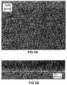
- FIGS. 2A and 2Bare top view and cross section view electron micrographs, respectively, of silicon nanowires grown from plated gold particles.
- the exemplary substrate shownis single crystal (111) p-type silicon covered with a dielectric stack composed of 10 nm SiO 2 and 20 nm Si 3 N 4 . Vias of 200 nm diameter were formed by UV lithography and reactive ion etching. Before the gold plating, the substrate was cleaned in 1:100 aqueous HF solution for 2 minutes.
- the patterned substrateis mounted on to plating apparatus with the electrical contact made through the backside of the substrate.
- the gold nanoparticleswere electroplated in a gold solution containing about 5 mM Au at a current density of about ⁇ 50 mA/cm 2 for about 1.5 seconds.
- the substratewas under illumination during the electroplating.
- the substrate with the plated goldwas then cleaned in 1:100 aqueous HF solution for about 1 minute, annealed in forming gas at about 400° C. for about 1 hour, cleaned again in 1:25 aqueous HF solution for about 30 seconds, and then loaded into a growth chamber for silicon nanowire growth.
- the wires shown in FIGS. 2A and 2Bwere grown at about 450° C. for about 8 minutes with silane as the precursor.
- the top view image in FIG. 2Ashows that most of the wires are epitaxial to the (111) silicon substrate as they grow in three directions 120° to each other.
- the cross sectional image in FIG. 2Bshows that most of the wires grow either perpendicular to the substrate or in a direction of about 54° to the substrate surface, and are (111) and (110) wires, respectively.
- the (110) wirescorrespond to the wires in three directions on the top view image in FIG. 2A and the (111) wires could not be observed on top view image as their projection is obscured from this view by the corresponding metal particle.
- a feature that “forms on”, “is formed on”, and “is forming on” another feature, including where other similar variants of the term “form” is used,mean that the feature so formed is in at least partial contact with the other feature.
Landscapes
- Engineering & Computer Science (AREA)
- Chemical & Material Sciences (AREA)
- Physics & Mathematics (AREA)
- Microelectronics & Electronic Packaging (AREA)
- General Physics & Mathematics (AREA)
- Manufacturing & Machinery (AREA)
- Computer Hardware Design (AREA)
- Power Engineering (AREA)
- Condensed Matter Physics & Semiconductors (AREA)
- Crystallography & Structural Chemistry (AREA)
- Materials Engineering (AREA)
- Nanotechnology (AREA)
- Metallurgy (AREA)
- Organic Chemistry (AREA)
- Theoretical Computer Science (AREA)
- Mathematical Physics (AREA)
- Chemically Coating (AREA)
Abstract
Description
- The present invention relates to a method for forming self-aligned semiconductor nanowires. More particularly, this invention relates to a method of electrochemically or electrolessly depositing metal nanoparticles at specific locations on a substrate to catalyze formation of epitaxial semiconductor nanowires at these locations by vapor-liquid-solid growth process.
- Inorganic nanowires, sometimes referred to as “whiskers”, can be grown on surfaces by a vapor-liquid-solid (VLS) process as described in U.S. Pat. Nos. 3,493,431, 5,702,822, and 5,858,862. As disclosed therein, semiconductor nanowires grown by VLS process, such as Si, Ge, GaAs and InP nanowires, are of particular interest for fabricating integrated electronic devices based on nanowire field effect transistors (FETs). Nanowire FETs can exhibit the advantageous quantum effects and also allow for 3-dimensional device integration, and hence may provide a much higher device density than the current technologies. However, a key challenge for the integration of such nanowires into real device is the difficulty in placing the wires precisely at desired locations.
- There is an ongoing effort to understand and improve the growth process of epitaxial semiconductor. Growth of the semiconductor wires by VLS process generally requires catalytic metal particles, such as Au or In particles. The metal particle(s direct the growth of the wires by catalyzing the formation of the nanowires at the interface of the substrate surface and the metal particles. The position of the wires is therefore determined by where the particle is placed. However, the present methods for growth of such nanowires provide non-site specific methods for depositing the catalytic metal particles and growing the nanowires, necessitating the use of methods such as lift-off layers or nanoimprint lithography to pattern the metal particles in order to direct the growth of nanowires.
- Accordingly, it is desirable to grow epitaxial nanowires selectively in predetermined locations on a surface of a substrate, using a method that avoids the use of potentially problematic, nonstandard, or highly specialized processing steps.
- The deficiencies of the prior art can be overcome by a method disclosed herein of forming self-aligned epitaxial semiconductor nanowires on substrates. More specifically, disclosed herein is a method of electrochemically or electrolessly depositing the catalytic nanoparticles in predetermined regions on silicon substrates, and thus growing the semiconductor nanowires.
- In an embodiment, a method of forming a nanostructure comprising nanowires, comprises: forming a mask on a surface of a substrate, wherein the mask has at least one opening to expose a portion of the surface of the masked substrate; depositing metal particles of a metal or metal alloy for catalyzing semiconductor nanowire growth on the exposed surface of the masked substrate to form a plated substrate; and growing nanowires on the plated substrate with the location of the nanowires defined by the plated metal particles. In an embodiment, the nanowires are grown by a vapor-liquid-solid (VLS) process with a nanowire precursor gas.
- In another embodiment, a method of forming a nanostructure comprises: forming a mask on a surface of a substrate, wherein the mask has at least one opening to expose a portion of the surface of the masked substrate; cleaning the exposed surface of the masked substrate with dilute aqueous hydrofluoric acid solution; plating metal particles of a metal for catalyzing semiconductor nanowire growth on the exposed surface of the masked substrate to form a plated substrate by immersing the masked substrate and an anode into a plating solution containing a metal particle precursor for the metal particles, and applying an electrical plating current for a predetermined time across the masked substrate and anode, wherein the metal particle precursor is gold, indium, or alloys thereof, the plating current is −1 mA/cm2to −100 mA/cm2, the plating time is less than or equal to 10 seconds, and light illumination is optionally applied to the masked substrate, wherein the size and the density of the metal particles are tuned by changing plating conditions comprising plating current, plating potential, plating time, agitation, temperature, illumination of the substrate, concentration of the metal species in the plating solution, addition of other chemical species to the plating solution, concentration of other chemical species in the plating solution, or a combination comprising at least one of these plating conditions; cleaning the plated substrate with dilute aqueous hydrofluoric acid solution; annealing the plated substrate prior to growing nanowires, wherein annealing is carried out at 300 to 550° C. for 10 minutes to 2 hours in an inert or reducing atmosphere, cleaning the plated substrate after annealing, with dilute aqueous hydrofluoric acid solution, and growing nanowires on the plated substrate with a nanowire precursor gas by a vapor-liquid-solid (VLS) process.
- In another embodiment, a method of forming a nanostructure comprises: forming a mask on a surface of a substrate, wherein the mask has at least one opening to expose a portion of the surface of the masked substrate; cleaning the exposed surface of the masked substrate with dilute aqueous hydrofluoric acid solution; plating metal particles of a metal for catalyzing semiconductor nanowire growth on the exposed surface of the masked substrate to form a plated substrate by immersing the masked substrate into a plating solution containing a metal particle precursor for the metal particles, and a reducing agent, wherein plating is carried out at 10° C. to 90° C., with or without agitation, and the plating time is 1 second to 30 minutes, wherein the size and density of the metal particles are tuned by changing plating conditions comprising immersion time, agitation, temperature, illumination, concentration of the metal particle precursor, identity and concentration of the reducing agents in the plating solution, addition of other chemical species in the plating solution, concentration of other chemical species in the plating solution, or a combination comprising at least one of these plating conditions; cleaning the plated substrate with dilute aqueous hydrofluoric acid solution; annealing the plated substrate prior to growing nanowires, wherein annealing is carried out at 300 to 550° C. for 10 minutes to 2 hours in an inert or reducing atmosphere, cleaning the plated substrate after annealing, with dilute aqueous hydrofluoric acid solution, and growing nanowires on the plated substrate with a nanowire precursor gas by a vapor-liquid-solid (VLS) process with the location of the nanowires defined by the plated metal particles.
- In another embodiment, a nanostructure prepared by an above-described method is disclosed. Also in an embodiment, the nanowires grow on the exposed region on the substrate and are epitaxial to the substrate. The silicon nanowires are from 1 to 100 nm in diameter. The length of the wires can be 0.1 μm to 100 μm depending on the growth time.
- Still other advantages of the present invention will become readily apparent by those skilled in the art from the following detailed description, wherein it is shown and described in the preferred embodiments, by way of illustration of the best mode. As will be realized, the disclosure is capable of other and different embodiments, and its several details are capable of modifications without departing from the spirit of the disclosure. Accordingly, the description is to be regarded as illustrative in nature and not as restricted thereto.
FIG. 1 is a schematic diagram of an exemplary process for growing self-aligned epitaxial semiconductor nanowires from a patterned substrate; andFIG. 2 is a micrograph from a scanning electron microscope (SEM) of exemplary self-aligned epitaxial silicon nanowires formed according to the method of the present invention.- A method of producing self-aligned epitaxial semiconductor nanowires on substrates is disclosed. The method includes plating (i.e., depositing) metal particles on a patterned substrate having cleaned, exposed regions; annealing the plated metal particles on the substrate; and growing nanowires from the plated metal particles by a VLS process at a predetermined temperature in an apparatus having a chamber, with a nanowire precursor gas (e.g., silane SiH4for silicon nanowires; germane GeH4for germanium nanowires; and the like). The diameter of the nanowire prepared by this method is proportional to the size (i.e., diameter) of the metal particle, specifically to the diameter of the hemispherical metal particle as measured at the interface of the metal particle and the substrate. The method selectively provides metal particles for catalyzing growth of nanowires on the surface of the substrate to thereby provide patterns of metal particles on the surface of the substrate, using readily available methods and without need for potentially problematic or nonstandard patterning methods such as use of lift-off layers (LOL) or nanoimprint lithography.
- In one embodiment of the present invention, the metal particles are deposited by immersing the substrate into a electroplating solution containing one or more precursor metal species for a metal or metal alloy particle (e.g., gold, indium, alloys thereof, or the like, with an average particle size, i.e., the average diameter of the particles, of 1 to 100 nm but not limited thereto); electroplating the metal from the electrolyte solution selectively onto the substrate to form metal particles in the exposed regions. Exemplary plating solutions are described in U.S. Pat. Nos. 4,077,852, 4,744,871, 4,755,264. The size and the density of the metal particles can be tuned by changing the plating conditions including plating current, plating potential, plating time, agitation, temperature, illumination of the substrate, concentration of the metal species in the plating solution, addition of other chemical species to the plating solution, concentration of other chemical species in the plating solution, or a combination comprising at least one of the foregoing plating conditions.
- In another embodiment of the present invention, the metal particles are deposited by immersing the substrate into a electroless plating solution containing one or more precursor metal species for a metal or metal alloy particle (e.g., gold, indium, alloys thereof, or the like, with an average particle size of 1 to 100 nm, but not limited thereto) and at least one reducing agent. Metal particles are formed selectively onto the substrate in the exposed regions. Exemplary electroless plating solutions are described in U.S. Pat. Nos. 4,804,559, 5,160,373, 5,198,273, 5,935,306 and 6,855,191. The size and density of the metal particles can be tuned by changing plating conditions comprising the immersion time, agitation, temperature, illumination, concentration of the metal particle precursor, identity and concentration of the reducing agents in the plating solution, addition of other chemical species in the plating solution, concentration of other chemical species in the plating solution, or a combination comprising at least one of these plating conditions.
- The nanowires as described herein are formed of one or more semiconducting materials that are of the same or different composition as that of the composition of the substrate. In an embodiment, the nanowire has a diameter of less than or equal to 100 nm, specifically less than or equal to 50 nm, and more specifically less than or equal to 20 nm. In an embodiment, the nanowire has a diameter of greater than or equal to 1 nm, specifically greater than or equal to 3 nm, and more specifically greater than or equal to 5 nm. Also in an embodiment, the nanowire has a length of 0.1 μm to 100 μm, and specifically 1 μm to 10 μm.
- The nanowires are included as a portion of a nanostructure, where the nanostructure is formed on an exposed surface of the substrate through a mask formed on the surface of the substrate. The mask is patterned to have one or more openings, which define the locations of the nanostructure, and which expose the underlying surface of the substrate. The opening in the mask is not limited as to size or shape, and can be regular or irregular, symmetric or asymmetric, simple in structure such as exemplified by a contact hole or trench, or complex in structure as for example where more than one such contact hole or trench is present in the nanostructure. In an embodiment, the nanostructure is not limited in size and can have a largest dimension of 0.1 μm to 100 μm.
- One or more whisker structures (i.e., nanowires) are included on the substrate exposed through the openings in the mask, where the nanowires so formed using the above method are in contact with and epitaxial to the substrate.
- Thus, in an embodiment, a method of forming a nanostructure comprising nanowires includes forming a mask on a surface of a substrate, wherein the mask has at least one opening to expose the surface of the substrate; plating metal or metal alloy particles on the exposed surface of the substrate to form a plated substrate by immersing the masked substrate and an anode into a plating solution containing a metal precursor for the metal particles, and applying an electrical potential across the masked substrate and anode; and growing nanowires on the plated substrate by a VLS semiconductor whisker growth method.
- The method is further illustrated in the figures, and a description of the exemplary embodiments is provided herein.
FIGS. 1A to 1C illustrate a method used to grow the self-aligned semiconductor nanowires in this invention.FIG. 1A is the schematic diagram of a patternedsubstrate 100 on which the semiconducting nanowires are to be formed. The patternedsubstrate 100 can be prepared by depositing adielectric layer 102 on a surface of asubstrate 101, and patterning thedielectric layer 102 to formopen regions 103.- Useful materials for the
substrate 101 include but are not limited to: Si-based or Ge-based semiconductors such as Si, Ge, or SiGe alloys; group III-V semiconductors such as GaAs or InP; and group II-VI semiconductors such as ZnO, ZnS or CdS; or a combination comprising at least one of the foregoing semiconductors. The substrate can also comprise a conductive material including but not limited to NiSi, PtSi and FeSi. The substrate can include one or more layers, including a combination of dielectric, conducting, and semiconducting layers, such as, in an embodiment, silicon-on-insulator (SOI) or like multilayer substrates. In a specific embodiment, the substrate is a semiconducting substrate. - Useful dielectric materials for
layer 102 include but are not limited to: SiO2, Si3N4, SiON, Al2O3, SiCO, fluorinated silica glass (FSG), organic silicate glass (OSG), spin-on glass (SOG), or the like, or a combination comprising at least one of the foregoing dielectric materials. Where a combination of dielectric materials is used, the materials are desirably deposited in sequential layers, where any number of layers may be used. Also, where a combination of dielectric materials is deposited in sequential layers, no particular order to the layers is required by the method, but it is contemplated that suitable combinations of dielectric materials within the scope of the present invention will become apparent to one skilled in the art in the practice of the invention as disclosed herein. - Patterning processes can be used after deposition of the
dielectric layer 102 to createopen regions 103 in thedielectric layer 102, where the surface of thesubstrate 101 is partially exposed through theopen regions 103. Useful patterning processes for forming the patterns (i.e., open regions103) in thedielectric layer 102 include but are not limited to standard photolithography methods including for example those carried out at UV wavelengths including g-Line (436 nm), i-Line (365 nm), DUV 248 nm, and 193 nm wavelengths, electron beam lithography, x-ray lithography, self alignment of diblock copolymers, reactive ion etch, or a combination comprising at least one of the foregoing processes. FIG. 1B is a schematic diagram showing thenanoparticles 103 plated in the exposed (i.e., patterned) region on thesubstrate 100, according to one embodiment of the present invention. Thesubstrate 100 is cleaned in a dilute HF solution and rinsed with water before plating. A typical cleaning is performed in a dilute (e.g., 1 part HF to 100 parts water, i.e., 1:100) aqueous hydrofluoric acid (HF) solution for 5 seconds to 5 minutes, depending on the nature of the substrate and the thickness and nature of the patterned dielectric layer. The composition and thickness of the dielectric layer are chosen such that it withstands the HF cleaning processes and the immersion in the subsequent plating solution. The plating can be carried out in a solution containing metals such as gold, indium, or other metal species that can catalyze the semiconductor nanowire growth. The plating solution can optionally include other chemical species that change the size and density of the plated metal particles. Chemical species for changing size and density of the metal particles include, but are not limited to, inorganic species such as Tl, Sb, As, I; chelating agents such as citrate, tartrate, ethylenediaminetetraacetic acid (EDTA); organic additives such as thiourea; and other inhibitors, accelerators, and levelers. The plating can be carried out with or without agitation. The plating current is typically −1 mA/cm2to −100 mA/cm2, and the plating time is typically less than or equal to 10 seconds depending on the plating solution, plating conditions, and the desired particle size. The plating can be carried out at any temperature where solution is stable, typically at 5° C. to 90° C., and more typically 20° C. to 60° C. The plating can be carried out with or without illumination depending on the nature of thesubstrate 101.- In another embodiment, the
nanoparticles 103 are deposited by immersing thesubstrate 100 into an electroless plating solution. Thesubstrate 100 is cleaned in a dilute HF solution and rinsed with water before plating. The plating solution contains one or more reducing agents and metal species such as gold, indium, or other metal species that can catalyze the semiconductor nanowire growth. The plating solution can optionally contain other chemical species that changes the size and density of the plated metal particles. Typical chemical species includes but not limited to inorganic species such as Tl, Sb, As, I; chelating agents such as citrate, tartrate, ethylenediaminetetraacetic acid (EDTA); organic additives such as thiourea; and other inhibitors, accelerators and levelers. The plating can be carried out at 10° C. to 90° C., and more specifically 30° C. to 90° C. The plating can be carried out with or without agitation. The plating time can be 1 second to 30 minutes depending on the plating solution, plating conditions and the desired particle size. FIG. 1C is the schematic diagram showing the semiconductor nanowires grown in theopen area 103 from the platedcatalyst particles 104.Catalyst particles 104, which melt at the high temperature used during the nanowire growth step, flatten at the point of contact with the surface and as such are typically roughly hemispherical in shape. After the plating ofcatalyst particles 104, thesubstrate 100 is cleaned in a dilute aqueous HF solution, typically in a 1:100 aqueous HF solution, for typically about 2 minutes. Immediately after the cleaning, an annealing process is carried out in an inert or reducing environment, such as for example in the presence of a gas including nitrogen, helium, argon, forming gas (e.g., a combination of up to 10 vol % hydrogen in nitrogen), or other inert or reducing environment. A typical condition for annealing is 300 to 550° C. for about 10 minutes to about 2 hours. Thesubstrate 100 is then cleaned in dilute aqueous HF and transferred into a vacuum chamber for nanowire growth. The growth of the nanowires can be carried out according to a known method. The point of growth of thenanowires 105 is at the interface of the flattened portion of thecatalyst particles 104, initially with the underlying surface ofsubstrate 101 exposed inopen area 103, and subsequently with the portion of thenanowires 105 in contact with thecatalyst particle 104 where the nanowire growth occurs. Thesemiconductor nanowires 105 that can be grown include but are not limited to those formed of semiconductors including: Si, Ge, SiGe, SiC, group III-V semiconductors such as InP, group II-VI semiconductors such as ZnO, or a combination comprising at least one of the foregoing semiconductors.- An exemplary process for making nanowires is as follows.
FIGS. 2A and 2B are top view and cross section view electron micrographs, respectively, of silicon nanowires grown from plated gold particles. The exemplary substrate shown is single crystal (111) p-type silicon covered with a dielectric stack composed of 10 nm SiO2and 20 nm Si3N4. Vias of 200 nm diameter were formed by UV lithography and reactive ion etching. Before the gold plating, the substrate was cleaned in 1:100 aqueous HF solution for 2 minutes. - The patterned substrate is mounted on to plating apparatus with the electrical contact made through the backside of the substrate. The gold nanoparticles were electroplated in a gold solution containing about 5 mM Au at a current density of about −50 mA/cm2for about 1.5 seconds. The substrate was under illumination during the electroplating. The substrate with the plated gold was then cleaned in 1:100 aqueous HF solution for about 1 minute, annealed in forming gas at about 400° C. for about 1 hour, cleaned again in 1:25 aqueous HF solution for about 30 seconds, and then loaded into a growth chamber for silicon nanowire growth. The wires shown in
FIGS. 2A and 2B were grown at about 450° C. for about 8 minutes with silane as the precursor. - The top view image in
FIG. 2A shows that most of the wires are epitaxial to the (111) silicon substrate as they grow in three directions 120° to each other. The cross sectional image inFIG. 2B shows that most of the wires grow either perpendicular to the substrate or in a direction of about 54° to the substrate surface, and are (111) and (110) wires, respectively. The (110) wires correspond to the wires in three directions on the top view image inFIG. 2A and the (111) wires could not be observed on top view image as their projection is obscured from this view by the corresponding metal particle. - The foregoing description illustrates and describes the present disclosure. Additionally, the disclosure shows and describes only the preferred embodiments of the disclosure, but, as mentioned above, it is to be understood that the invention is capable of changes or modifications within the scope of the concept as expressed herein, commensurate with the above teachings and/or skill or knowledge of the relevant art and without departing from the spirit of the invention. For instance, the features or steps can be performed in a differing order, or the features or steps can be added, deleted or modified. All of these variations are considered a part of the claimed invention. The embodiments described hereinabove are further intended to explain best modes known of practicing the invention and to enable others skilled in the art to utilize the disclosure in such, or other, embodiments and with the various modifications required by the particular applications or used disclosed herein. Accordingly, the description is not intended to limit the invention to the form disclosed herein.
- All publications, patents and patent applications cited in this specification are herein incorporated by reference, and for any and all purposed, as if each individual publication, patent or patent application were specifically and individually indicates to be incorporated by reference. In the case of inconsistencies, the present disclosure will prevail.
- The term “comprising” (and its grammatical variations) as used herein is used in the inclusive sense of “having” or “including” and not in the exclusive sense of “consisting only of”. The singular forms “a,” “an,” and “the” include plural referents unless the context clearly dictates otherwise. The endpoints of all ranges reciting the same characteristic or component are independently combinable and inclusive of the recited endpoint. All references are incorporated herein by reference. The terms “first,” “second,” and the like herein do not denote any order, quantity, or importance, but rather are used to distinguish one element from another. As used herein and unless otherwise specified, a feature that “forms on”, “is formed on”, and “is forming on” another feature, including where other similar variants of the term “form” is used, mean that the feature so formed is in at least partial contact with the other feature.
- While the preferred embodiment to the invention has been described, it will be understood that those skilled in the art, both now and in the future, may make various improvements and enhancements which fall within the scope of the claims which follow.
Claims (20)
Priority Applications (1)
| Application Number | Priority Date | Filing Date | Title |
|---|---|---|---|
| US11/674,453US20080191317A1 (en) | 2007-02-13 | 2007-02-13 | Self-aligned epitaxial growth of semiconductor nanowires |
Applications Claiming Priority (1)
| Application Number | Priority Date | Filing Date | Title |
|---|---|---|---|
| US11/674,453US20080191317A1 (en) | 2007-02-13 | 2007-02-13 | Self-aligned epitaxial growth of semiconductor nanowires |
Publications (1)
| Publication Number | Publication Date |
|---|---|
| US20080191317A1true US20080191317A1 (en) | 2008-08-14 |
Family
ID=39685118
Family Applications (1)
| Application Number | Title | Priority Date | Filing Date |
|---|---|---|---|
| US11/674,453AbandonedUS20080191317A1 (en) | 2007-02-13 | 2007-02-13 | Self-aligned epitaxial growth of semiconductor nanowires |
Country Status (1)
| Country | Link |
|---|---|
| US (1) | US20080191317A1 (en) |
Cited By (22)
| Publication number | Priority date | Publication date | Assignee | Title |
|---|---|---|---|---|
| US20080093693A1 (en)* | 2006-10-20 | 2008-04-24 | Kamins Theodore I | Nanowire sensor with variant selectively interactive segments |
| US20080132052A1 (en)* | 2006-12-05 | 2008-06-05 | Electronics And Telecommunications Research Institute | Method of fabricating electronic device using nanowires |
| US20100090345A1 (en)* | 2008-10-10 | 2010-04-15 | Uchicago Argonne, Llc | Direct growth of metal nanoplates on semiconductor substrates |
| FR2941688A1 (en)* | 2009-01-30 | 2010-08-06 | Commissariat Energie Atomique | PROCESS FOR FORMING NANO-THREADS |
| WO2011014408A1 (en)* | 2009-07-29 | 2011-02-03 | Massachusetts Institute Of Technology | Nanowire synthesis |
| US20110073839A1 (en)* | 2009-09-30 | 2011-03-31 | Kahen Keith B | Ii-vi semiconductor nanowires |
| US20110076841A1 (en)* | 2009-09-30 | 2011-03-31 | Kahen Keith B | Forming catalyzed ii-vi semiconductor nanowires |
| US20110165761A1 (en)* | 2009-12-07 | 2011-07-07 | Kim Myung-Jong | Methods of fabricating semiconductor devices and semiconductor devices fabricated by the same |
| US20120112157A1 (en)* | 2009-07-20 | 2012-05-10 | Quitoriano Nathaniel J | Nanowire sensor with angled segments that are differently functionalized |
| WO2012080252A1 (en)* | 2010-12-13 | 2012-06-21 | Norwegian University Of Science And Technology (Ntnu) | Nanowire epitaxy on a graphitic substrate |
| US20150076450A1 (en)* | 2012-01-10 | 2015-03-19 | Norwegian University Of Science And Technology (Ntnu) | Nanowire device having graphene top and bottom electrodes and method of making such a device |
| US20150125601A1 (en)* | 2013-11-04 | 2015-05-07 | Systems And Materials Research Corporation | Method and apparatus for producing nanosilicon particles |
| US10243061B1 (en) | 2017-11-15 | 2019-03-26 | International Business Machines Corporation | Nanosheet transistor |
| US10249740B2 (en)* | 2015-06-27 | 2019-04-02 | Intel Corporation | Ge nano wire transistor with GaAs as the sacrificial layer |
| US10347791B2 (en) | 2015-07-13 | 2019-07-09 | Crayonano As | Nanowires or nanopyramids grown on graphitic substrate |
| US10347781B2 (en) | 2012-06-21 | 2019-07-09 | Norwegian University Of Science And Technology (Ntnu) | Solar cells |
| US10714337B2 (en) | 2015-07-31 | 2020-07-14 | Crayonano As | Process for growing nanowires or nanopyramids on graphitic substrates |
| WO2021234462A3 (en)* | 2020-05-19 | 2021-12-30 | Alignedbio Ab | Method of growing semiconductor nanowires using a catalyst alloy |
| US11239391B2 (en) | 2017-04-10 | 2022-02-01 | Norwegian University Of Science And Technology (Ntnu) | Nanostructure |
| US11261537B2 (en) | 2013-06-21 | 2022-03-01 | Norwegian University Of Science And Technology (Ntnu) | III-V or II-VI compound semiconductor films on graphitic substrates |
| US11594657B2 (en) | 2015-07-13 | 2023-02-28 | Crayonano As | Nanowires/nanopyramids shaped light emitting diodes and photodetectors |
| US11652161B2 (en) | 2016-09-20 | 2023-05-16 | Tessera Llc | Nanosheet channel-to-source and drain isolation |
Citations (19)
| Publication number | Priority date | Publication date | Assignee | Title |
|---|---|---|---|---|
| US3493431A (en)* | 1966-11-25 | 1970-02-03 | Bell Telephone Labor Inc | Vapor-liquid-solid crystal growth technique |
| US4077852A (en)* | 1977-02-09 | 1978-03-07 | Bell Telephone Laboratories, Incorporated | Selective gold plating |
| US4744871A (en)* | 1986-09-25 | 1988-05-17 | Vanguard Research Associates, Inc. | Electrolyte solution and process for gold electroplating |
| US4755264A (en)* | 1987-05-29 | 1988-07-05 | Vanguard Research Associates, Inc. | Electrolyte solution and process for gold electroplating |
| US4804559A (en)* | 1985-10-14 | 1989-02-14 | Hitachi, Ltd. | Electroless gold plating solution |
| US5160373A (en)* | 1991-04-26 | 1992-11-03 | Murata Manufacturing Co., Ltd. | Electroless plating bath |
| US5198273A (en)* | 1989-09-18 | 1993-03-30 | Hitachi, Ltd. | Electroless gold plating solution and method for plating gold therewith |
| US5314569A (en)* | 1990-02-23 | 1994-05-24 | Thomson-Csf | Method for the controlled growth of crystal whiskers and application thereof to the making of tip microcathodes |
| US5702822A (en)* | 1992-05-22 | 1997-12-30 | Denki Kagaku Kogyo Kabushiki Kaisha | Method for producing single crystal, and needle-like single crystal |
| US5858862A (en)* | 1996-09-25 | 1999-01-12 | Sony Corporation | Process for producing quantum fine wire |
| US5935306A (en)* | 1998-02-10 | 1999-08-10 | Technic Inc. | Electroless gold plating bath |
| US6130143A (en)* | 1996-10-28 | 2000-10-10 | Sony Corporation | Quantum wires formed on a substrate, manufacturing method thereof, and device having quantum wires on a substrate |
| US20020072069A1 (en)* | 2000-12-08 | 2002-06-13 | William Ford | Linker molecules for selective metallisation of nucleic acids and their uses |
| US20020125805A1 (en)* | 2001-03-09 | 2002-09-12 | Hsu David S. Y. | Self-aligned integrally gated nanofilament field emitter cell and array |
| US20040058153A1 (en)* | 2002-04-29 | 2004-03-25 | Boston College | Density controlled carbon nanotube array electrodes |
| US6831017B1 (en)* | 2002-04-05 | 2004-12-14 | Integrated Nanosystems, Inc. | Catalyst patterning for nanowire devices |
| US20050011431A1 (en)* | 2003-04-04 | 2005-01-20 | Btg International Limited | Precisely positioned nanowhiskers and nanowhisker arrays and method for preparing them |
| US6855191B2 (en)* | 2002-01-30 | 2005-02-15 | Kanto Kagaku Kabushiki Kaisha | Electroless gold plating solution |
| US7255745B2 (en)* | 2004-10-21 | 2007-08-14 | Sharp Laboratories Of America, Inc. | Iridium oxide nanowires and method for forming same |
- 2007
- 2007-02-13USUS11/674,453patent/US20080191317A1/ennot_activeAbandoned
Patent Citations (19)
| Publication number | Priority date | Publication date | Assignee | Title |
|---|---|---|---|---|
| US3493431A (en)* | 1966-11-25 | 1970-02-03 | Bell Telephone Labor Inc | Vapor-liquid-solid crystal growth technique |
| US4077852A (en)* | 1977-02-09 | 1978-03-07 | Bell Telephone Laboratories, Incorporated | Selective gold plating |
| US4804559A (en)* | 1985-10-14 | 1989-02-14 | Hitachi, Ltd. | Electroless gold plating solution |
| US4744871A (en)* | 1986-09-25 | 1988-05-17 | Vanguard Research Associates, Inc. | Electrolyte solution and process for gold electroplating |
| US4755264A (en)* | 1987-05-29 | 1988-07-05 | Vanguard Research Associates, Inc. | Electrolyte solution and process for gold electroplating |
| US5198273A (en)* | 1989-09-18 | 1993-03-30 | Hitachi, Ltd. | Electroless gold plating solution and method for plating gold therewith |
| US5314569A (en)* | 1990-02-23 | 1994-05-24 | Thomson-Csf | Method for the controlled growth of crystal whiskers and application thereof to the making of tip microcathodes |
| US5160373A (en)* | 1991-04-26 | 1992-11-03 | Murata Manufacturing Co., Ltd. | Electroless plating bath |
| US5702822A (en)* | 1992-05-22 | 1997-12-30 | Denki Kagaku Kogyo Kabushiki Kaisha | Method for producing single crystal, and needle-like single crystal |
| US5858862A (en)* | 1996-09-25 | 1999-01-12 | Sony Corporation | Process for producing quantum fine wire |
| US6130143A (en)* | 1996-10-28 | 2000-10-10 | Sony Corporation | Quantum wires formed on a substrate, manufacturing method thereof, and device having quantum wires on a substrate |
| US5935306A (en)* | 1998-02-10 | 1999-08-10 | Technic Inc. | Electroless gold plating bath |
| US20020072069A1 (en)* | 2000-12-08 | 2002-06-13 | William Ford | Linker molecules for selective metallisation of nucleic acids and their uses |
| US20020125805A1 (en)* | 2001-03-09 | 2002-09-12 | Hsu David S. Y. | Self-aligned integrally gated nanofilament field emitter cell and array |
| US6855191B2 (en)* | 2002-01-30 | 2005-02-15 | Kanto Kagaku Kabushiki Kaisha | Electroless gold plating solution |
| US6831017B1 (en)* | 2002-04-05 | 2004-12-14 | Integrated Nanosystems, Inc. | Catalyst patterning for nanowire devices |
| US20040058153A1 (en)* | 2002-04-29 | 2004-03-25 | Boston College | Density controlled carbon nanotube array electrodes |
| US20050011431A1 (en)* | 2003-04-04 | 2005-01-20 | Btg International Limited | Precisely positioned nanowhiskers and nanowhisker arrays and method for preparing them |
| US7255745B2 (en)* | 2004-10-21 | 2007-08-14 | Sharp Laboratories Of America, Inc. | Iridium oxide nanowires and method for forming same |
Cited By (44)
| Publication number | Priority date | Publication date | Assignee | Title |
|---|---|---|---|---|
| US20080093693A1 (en)* | 2006-10-20 | 2008-04-24 | Kamins Theodore I | Nanowire sensor with variant selectively interactive segments |
| US7951698B2 (en)* | 2006-12-05 | 2011-05-31 | Electronics And Telecommunications Research Institute | Method of fabricating electronic device using nanowires |
| US20080132052A1 (en)* | 2006-12-05 | 2008-06-05 | Electronics And Telecommunications Research Institute | Method of fabricating electronic device using nanowires |
| US8247325B2 (en)* | 2008-10-10 | 2012-08-21 | Uchicago Argonne, Llc | Direct growth of metal nanoplates on semiconductor substrates |
| US20100090345A1 (en)* | 2008-10-10 | 2010-04-15 | Uchicago Argonne, Llc | Direct growth of metal nanoplates on semiconductor substrates |
| FR2941688A1 (en)* | 2009-01-30 | 2010-08-06 | Commissariat Energie Atomique | PROCESS FOR FORMING NANO-THREADS |
| US8569151B2 (en) | 2009-01-30 | 2013-10-29 | Commissariat A L'energie Atomique Et Aux Energies Alternatives | Method of formation of nanowires and method of manufacture of associated optical component |
| US20120112157A1 (en)* | 2009-07-20 | 2012-05-10 | Quitoriano Nathaniel J | Nanowire sensor with angled segments that are differently functionalized |
| US8569900B2 (en)* | 2009-07-20 | 2013-10-29 | Hewlett-Packard Development Company, L.P. | Nanowire sensor with angled segments that are differently functionalized |
| WO2011014408A1 (en)* | 2009-07-29 | 2011-02-03 | Massachusetts Institute Of Technology | Nanowire synthesis |
| US20110073839A1 (en)* | 2009-09-30 | 2011-03-31 | Kahen Keith B | Ii-vi semiconductor nanowires |
| US20110076841A1 (en)* | 2009-09-30 | 2011-03-31 | Kahen Keith B | Forming catalyzed ii-vi semiconductor nanowires |
| WO2011041274A1 (en)* | 2009-09-30 | 2011-04-07 | Eastman Kodak Company | Forming catalyzed ii-vi semiconductor nanowires |
| US8274138B2 (en)* | 2009-09-30 | 2012-09-25 | Eastman Kodak Company | II-VI semiconductor nanowires |
| US20110165761A1 (en)* | 2009-12-07 | 2011-07-07 | Kim Myung-Jong | Methods of fabricating semiconductor devices and semiconductor devices fabricated by the same |
| US8420551B2 (en)* | 2009-12-07 | 2013-04-16 | Samsung Electronics Co., Ltd. | Methods of fabricating semiconductor devices and semiconductor devices fabricated by the same |
| US9966257B2 (en) | 2010-12-13 | 2018-05-08 | Norwegian University Of Science And Technology | Nanowire epitaxy on a graphitic substrate |
| US10861696B2 (en) | 2010-12-13 | 2020-12-08 | Norwegian University Of Science And Technology | Compositions comprising epitaxial nanowires on graphene substrates and methods of making thereof |
| CN103477418A (en)* | 2010-12-13 | 2013-12-25 | 挪威科技大学 | Nanowire epitaxy on a graphitic substrate |
| EA026823B1 (en)* | 2010-12-13 | 2017-05-31 | Норвегиан Юниверсити Оф Сайенс Энд Текнолоджи (Энтиэню) | Process for preparing a semiconductor nanostructure |
| CN103477418B (en)* | 2010-12-13 | 2017-09-01 | 挪威科技大学 | Nanowire Epitaxy on Graphite Substrates |
| WO2012080252A1 (en)* | 2010-12-13 | 2012-06-21 | Norwegian University Of Science And Technology (Ntnu) | Nanowire epitaxy on a graphitic substrate |
| US20150076450A1 (en)* | 2012-01-10 | 2015-03-19 | Norwegian University Of Science And Technology (Ntnu) | Nanowire device having graphene top and bottom electrodes and method of making such a device |
| US10243104B2 (en)* | 2012-01-10 | 2019-03-26 | Norwegian Univeresity Of Science And Technology (Ntnu) | Nanowire device having graphene top and bottom electrodes and method of making such a device |
| US11257967B2 (en) | 2012-06-21 | 2022-02-22 | Norwegian University Of Science And Technology (Ntnu) | Solar cells |
| US10347781B2 (en) | 2012-06-21 | 2019-07-09 | Norwegian University Of Science And Technology (Ntnu) | Solar cells |
| US11261537B2 (en) | 2013-06-21 | 2022-03-01 | Norwegian University Of Science And Technology (Ntnu) | III-V or II-VI compound semiconductor films on graphitic substrates |
| US20150125601A1 (en)* | 2013-11-04 | 2015-05-07 | Systems And Materials Research Corporation | Method and apparatus for producing nanosilicon particles |
| US10249740B2 (en)* | 2015-06-27 | 2019-04-02 | Intel Corporation | Ge nano wire transistor with GaAs as the sacrificial layer |
| US10930766B2 (en) | 2015-06-27 | 2021-02-23 | Intel Corporation | Ge NANO wire transistor with GAAS as the sacrificial layer |
| US11594657B2 (en) | 2015-07-13 | 2023-02-28 | Crayonano As | Nanowires/nanopyramids shaped light emitting diodes and photodetectors |
| US10347791B2 (en) | 2015-07-13 | 2019-07-09 | Crayonano As | Nanowires or nanopyramids grown on graphitic substrate |
| US11264536B2 (en) | 2015-07-13 | 2022-03-01 | Crayonano As | Nanowires or nanopyramids grown on a graphene substrate |
| US10714337B2 (en) | 2015-07-31 | 2020-07-14 | Crayonano As | Process for growing nanowires or nanopyramids on graphitic substrates |
| US11450528B2 (en) | 2015-07-31 | 2022-09-20 | Crayonano As | Process for growing nanowires or nanopyramids on graphitic substrates |
| US11652161B2 (en) | 2016-09-20 | 2023-05-16 | Tessera Llc | Nanosheet channel-to-source and drain isolation |
| US12166110B2 (en) | 2016-09-20 | 2024-12-10 | Adeia Semiconductor Solutions Llc | Nanosheet channel-to-source and drain isolation |
| US11239391B2 (en) | 2017-04-10 | 2022-02-01 | Norwegian University Of Science And Technology (Ntnu) | Nanostructure |
| US10727315B2 (en) | 2017-11-15 | 2020-07-28 | Tessera, Inc. | Nanosheet transistor |
| US11049953B2 (en) | 2017-11-15 | 2021-06-29 | Tessera, Inc. | Nanosheet transistor |
| US11901438B2 (en) | 2017-11-15 | 2024-02-13 | Adeia Semiconductor Solutions Llc | Nanosheet transistor |
| US10243061B1 (en) | 2017-11-15 | 2019-03-26 | International Business Machines Corporation | Nanosheet transistor |
| US12369379B2 (en) | 2017-11-15 | 2025-07-22 | Adeia Semiconductor Solutions Llc | Nanosheet transistor |
| WO2021234462A3 (en)* | 2020-05-19 | 2021-12-30 | Alignedbio Ab | Method of growing semiconductor nanowires using a catalyst alloy |
Similar Documents
| Publication | Publication Date | Title |
|---|---|---|
| US20080191317A1 (en) | Self-aligned epitaxial growth of semiconductor nanowires | |
| US8455333B2 (en) | Method for reuse of wafers for growth of vertically-aligned wire arrays | |
| US7718531B2 (en) | Method for forming catalyst nanoparticles for growing elongated nanostructures | |
| US7208094B2 (en) | Methods of bridging lateral nanowires and device using same | |
| US7579263B2 (en) | Threading-dislocation-free nanoheteroepitaxy of Ge on Si using self-directed touch-down of Ge through a thin SiO2 layer | |
| US6653209B1 (en) | Method of producing silicon thin film, method of constructing SOI substrate and semiconductor device | |
| US7566657B2 (en) | Methods of forming through-substrate interconnects | |
| US20070105356A1 (en) | Method of controlling nanowire growth and device with controlled-growth nanowire | |
| CN105190914B (en) | Process for depositing epitaxial ZnO on group III nitride based light emitting diodes and light emitting diodes comprising epitaxial ZnO | |
| CN101595565A (en) | Method for Fabricating Precision Vertical and Horizontal Layers on Vertical Semiconductor Structures | |
| US8859402B2 (en) | Method for making epitaxial structure | |
| US9105484B2 (en) | Epitaxial stucture | |
| JP2006349673A (en) | Nanowire sensor device and method of manufacturing nanowire sensor device structure | |
| CN107665820A (en) | The manufacture method of engraving method, the manufacture method of semiconductor chip and article | |
| US9647063B2 (en) | Nanoscale chemical templating with oxygen reactive materials | |
| KR101164113B1 (en) | Fabricating method of multi-diameter silicon wire structure | |
| JP2004511102A (en) | The process of revealing crystal defects and / or stress fields at the molecular bonding interface of two solid materials | |
| CN116648776A (en) | Defect-free germanium oxide gap fill | |
| CN113113512A (en) | Directional heteroepitaxy method and silicon-based germanium-tin alloy material | |
| TW202312265A (en) | etching method | |
| CN112382558B (en) | Preparation method of controllable quantum structure based on micro-nano metal/semiconductor Schottky junction | |
| JPH03125458A (en) | Method of forming single crystal region, and single crystal article using same | |
| KR20090018743A (en) | Selective metal silicide method of silicon-based nanowire surface and semiconductor device manufactured by the same | |
| Badawy | Synthesis of Catalyst-Free InAs Nanowires on Silicon | |
| US20090000539A1 (en) | Apparatus for growing a nanowire and method for controlling position of catalyst material |
Legal Events
| Date | Code | Title | Description |
|---|---|---|---|
| AS | Assignment | Owner name:INTERNATIONAL BUSINESS MACHINES CORPORATION, CONNE Free format text:ASSIGNMENT OF ASSIGNORS INTEREST;ASSIGNORS:COHEN, GUY MOSHE;DELIGIANNI, HARIKLIA;HUANG, QIANG;AND OTHERS;REEL/FRAME:018886/0751;SIGNING DATES FROM 20070207 TO 20070209 Owner name:INTERNATIONAL BUSINESS MACHINES CORPORATION, CONNE Free format text:ASSIGNMENT OF ASSIGNORS INTEREST;ASSIGNORS:COHEN, GUY MOSHE;DELIGIANNI, HARIKLIA;HUANG, QIANG;AND OTHERS;SIGNING DATES FROM 20070207 TO 20070209;REEL/FRAME:018886/0751 | |
| AS | Assignment | Owner name:INTERNATIONAL BUSINESS MACHINES CORPORATION, NEW Y Free format text:CORRECTIVE ASSIGNMENT TO CORRECT THE ADDRESS CORRECTION FOR ASSIGNEE ARMONK, CONNECTICUT TO ARMONK, NEW YORK. PREVIOUSLY RECORDED ON REEL 018886 FRAME 0751;ASSIGNORS:COHEN, GUY MOSHE;DELIGIANNI, HARIKLIA;HUANG, QIANG;AND OTHERS;REEL/FRAME:019048/0515;SIGNING DATES FROM 20070207 TO 20070209 Owner name:INTERNATIONAL BUSINESS MACHINES CORPORATION, NEW Y Free format text:CORRECTIVE ASSIGNMENT TO CORRECT THE ADDRESS CORRECTION FOR ASSIGNEE ARMONK, CONNECTICUT TO ARMONK, NEW YORK. PREVIOUSLY RECORDED ON REEL 018886 FRAME 0751. ASSIGNOR(S) HEREBY CONFIRMS THE CORRECTED ASSIGNMENT;ASSIGNORS:COHEN, GUY MOSHE;DELIGIANNI, HARIKLIA;HUANG, QIANG;AND OTHERS;SIGNING DATES FROM 20070207 TO 20070209;REEL/FRAME:019048/0515 | |
| STCB | Information on status: application discontinuation | Free format text:ABANDONED -- FAILURE TO RESPOND TO AN OFFICE ACTION | |
| AS | Assignment | Owner name:GLOBALFOUNDRIES U.S. 2 LLC, NEW YORK Free format text:ASSIGNMENT OF ASSIGNORS INTEREST;ASSIGNOR:INTERNATIONAL BUSINESS MACHINES CORPORATION;REEL/FRAME:036550/0001 Effective date:20150629 | |
| AS | Assignment | Owner name:GLOBALFOUNDRIES INC., CAYMAN ISLANDS Free format text:ASSIGNMENT OF ASSIGNORS INTEREST;ASSIGNORS:GLOBALFOUNDRIES U.S. 2 LLC;GLOBALFOUNDRIES U.S. INC.;REEL/FRAME:036779/0001 Effective date:20150910 |