US20080188034A1 - Assemblies displaying differential negative resistance, semiconductor constructions, and methods of forming assemblies displaying differential negative resistance - Google Patents
Assemblies displaying differential negative resistance, semiconductor constructions, and methods of forming assemblies displaying differential negative resistanceDownload PDFInfo
- Publication number
- US20080188034A1 US20080188034A1US12/068,020US6802008AUS2008188034A1US 20080188034 A1US20080188034 A1US 20080188034A1US 6802008 AUS6802008 AUS 6802008AUS 2008188034 A1US2008188034 A1US 2008188034A1
- Authority
- US
- United States
- Prior art keywords
- layer
- negative resistance
- forming
- differential negative
- displaying differential
- Prior art date
- Legal status (The legal status is an assumption and is not a legal conclusion. Google has not performed a legal analysis and makes no representation as to the accuracy of the status listed.)
- Granted
Links
- 238000000034methodMethods0.000titleclaimsabstractdescription30
- 238000010276constructionMethods0.000titleabstractdescription33
- 238000000429assemblyMethods0.000titleabstractdescription14
- 230000000712assemblyEffects0.000titleabstractdescription14
- 239000004065semiconductorSubstances0.000titleabstractdescription10
- 229910052711seleniumInorganic materials0.000claimsabstractdescription26
- 229910052717sulfurInorganic materials0.000claimsabstractdescription22
- 229910052714telluriumInorganic materials0.000claimsabstractdescription22
- 229910052723transition metalInorganic materials0.000claimsabstractdescription11
- 150000003624transition metalsChemical class0.000claimsabstractdescription11
- 229910052760oxygenInorganic materials0.000claimsabstractdescription6
- 239000000463materialSubstances0.000claimsdescription51
- 239000004020conductorSubstances0.000claimsdescription28
- 229910052719titaniumInorganic materials0.000claimsdescription7
- ATJFFYVFTNAWJD-UHFFFAOYSA-NTinChemical compound[Sn]ATJFFYVFTNAWJD-UHFFFAOYSA-N0.000claimsdescription6
- 229910052718tinInorganic materials0.000claimsdescription6
- 239000010949copperSubstances0.000claimsdescription5
- 229910052697platinumInorganic materials0.000claimsdescription5
- RYGMFSIKBFXOCR-UHFFFAOYSA-NCopperChemical group[Cu]RYGMFSIKBFXOCR-UHFFFAOYSA-N0.000claimsdescription4
- 229910052802copperInorganic materials0.000claimsdescription3
- 239000000758substrateSubstances0.000abstractdescription16
- 229910052709silverInorganic materials0.000description19
- BQCADISMDOOEFD-UHFFFAOYSA-NSilverChemical compound[Ag]BQCADISMDOOEFD-UHFFFAOYSA-N0.000description17
- 239000004332silverSubstances0.000description17
- 239000012634fragmentSubstances0.000description9
- 229910052751metalInorganic materials0.000description8
- 239000002184metalSubstances0.000description8
- 238000004544sputter depositionMethods0.000description5
- 238000002207thermal evaporationMethods0.000description5
- BASFCYQUMIYNBI-UHFFFAOYSA-NplatinumChemical compound[Pt]BASFCYQUMIYNBI-UHFFFAOYSA-N0.000description4
- 238000000151depositionMethods0.000description3
- 239000000203mixtureSubstances0.000description3
- 239000010936titaniumSubstances0.000description3
- 229910052721tungstenInorganic materials0.000description3
- VYPSYNLAJGMNEJ-UHFFFAOYSA-NSilicium dioxideChemical compoundO=[Si]=OVYPSYNLAJGMNEJ-UHFFFAOYSA-N0.000description2
- 239000005380borophosphosilicate glassSubstances0.000description2
- 238000002425crystallisationMethods0.000description2
- 230000008025crystallizationEffects0.000description2
- 230000000694effectsEffects0.000description2
- 230000006870functionEffects0.000description2
- 150000002739metalsChemical class0.000description2
- 238000000059patterningMethods0.000description2
- 230000000737periodic effectEffects0.000description2
- WFKWXMTUELFFGS-UHFFFAOYSA-NtungstenChemical compound[W]WFKWXMTUELFFGS-UHFFFAOYSA-N0.000description2
- 239000010937tungstenSubstances0.000description2
- 229910001316Ag alloyInorganic materials0.000description1
- 229910000881Cu alloyInorganic materials0.000description1
- 229910052581Si3N4Inorganic materials0.000description1
- 229910004166TaNInorganic materials0.000description1
- RTAQQCXQSZGOHL-UHFFFAOYSA-NTitaniumChemical compound[Ti]RTAQQCXQSZGOHL-UHFFFAOYSA-N0.000description1
- NRTOMJZYCJJWKI-UHFFFAOYSA-NTitanium nitrideChemical compound[Ti]#NNRTOMJZYCJJWKI-UHFFFAOYSA-N0.000description1
- 229910045601alloyInorganic materials0.000description1
- 239000000956alloySubstances0.000description1
- 239000000470constituentSubstances0.000description1
- 239000006185dispersionSubstances0.000description1
- 238000001704evaporationMethods0.000description1
- -1for exampleChemical class0.000description1
- 239000011521glassSubstances0.000description1
- 238000010348incorporationMethods0.000description1
- 238000004519manufacturing processMethods0.000description1
- 229910001092metal group alloyInorganic materials0.000description1
- 238000012986modificationMethods0.000description1
- 230000004048modificationEffects0.000description1
- 229910021421monocrystalline siliconInorganic materials0.000description1
- 235000012239silicon dioxideNutrition0.000description1
- 239000000377silicon dioxideSubstances0.000description1
- HQVNEWCFYHHQES-UHFFFAOYSA-Nsilicon nitrideChemical compoundN12[Si]34N5[Si]62N3[Si]51N64HQVNEWCFYHHQES-UHFFFAOYSA-N0.000description1
- 239000000126substanceSubstances0.000description1
- 239000011135tinSubstances0.000description1
- 230000007704transitionEffects0.000description1
- 230000005641tunnelingEffects0.000description1
Images


Classifications
- H—ELECTRICITY
- H10—SEMICONDUCTOR DEVICES; ELECTRIC SOLID-STATE DEVICES NOT OTHERWISE PROVIDED FOR
- H10N—ELECTRIC SOLID-STATE DEVICES NOT OTHERWISE PROVIDED FOR
- H10N80/00—Bulk negative-resistance effect devices
- H10N80/01—Manufacture or treatment
- H—ELECTRICITY
- H10—SEMICONDUCTOR DEVICES; ELECTRIC SOLID-STATE DEVICES NOT OTHERWISE PROVIDED FOR
- H10D—INORGANIC ELECTRIC SEMICONDUCTOR DEVICES
- H10D62/00—Semiconductor bodies, or regions thereof, of devices having potential barriers
- H10D62/80—Semiconductor bodies, or regions thereof, of devices having potential barriers characterised by the materials
- H10D62/82—Heterojunctions
- H—ELECTRICITY
- H10—SEMICONDUCTOR DEVICES; ELECTRIC SOLID-STATE DEVICES NOT OTHERWISE PROVIDED FOR
- H10D—INORGANIC ELECTRIC SEMICONDUCTOR DEVICES
- H10D8/00—Diodes
- H10D8/70—Tunnel-effect diodes
- H—ELECTRICITY
- H10—SEMICONDUCTOR DEVICES; ELECTRIC SOLID-STATE DEVICES NOT OTHERWISE PROVIDED FOR
- H10N—ELECTRIC SOLID-STATE DEVICES NOT OTHERWISE PROVIDED FOR
- H10N80/00—Bulk negative-resistance effect devices
Definitions
- the inventionpertains to semiconductor constructions, such as, for example, assemblies displaying differential negative resistance.
- the inventionalso pertains to methods of forming assemblies displaying differential negative resistance.
- the assemblies displaying differential negative resistanceare tunnel diode assemblies.
- Assemblies displaying differential negative resistancecan be used as components in various types of circuits, including, for example, logic circuits, and microwave oscillators. It can therefore be desired to incorporate assemblies displaying differential negative resistance into integrated circuit structures.
- DNRdifferential negative resistance
- the ratio of the current at the peak to the current at the valleycan be utilized as a figure-of-merit for a device displaying differential negative resistance. Higher peak-to-valley ratios are considered to indicate better-quality devices. Presently, the highest peak-to-valley ratios obtained for integrated circuit tunnel diode devices are less than 8. It would be desirable to develop better devices displaying differential negative resistance which can be incorporated into integrated circuits.
- the inventionpertains to a device displaying differential negative resistance characterized by a current-versus-voltage profile having a peak-to-valley ratio of at least about 9.
- the inventionpertains to a semiconductor construction comprising a substrate, and a first layer over the substrate.
- the first layercomprises Ge and one or more of S, Te and Se.
- a second layeris over the first layer.
- the second layercomprises M and A, where M is a transition metal and A is one or more of O, S, Te and Se.
- a third layeris over the second layer, and comprises Ge and one or more of S, Te and Se. The first, second and third layers are together incorporated into an assembly displaying differential negative resistance.
- the inventionencompasses a semiconductor construction which includes a substrate and an assembly displaying differential negative resistance supported by the substrate.
- the assemblycomprises a material which includes Ge, a transition metal, and one or more of S, Te and Se.
- the inventionalso encompasses methodology for forming the constructions and structures described above.
- FIG. 1is a diagrammatic, cross-sectional view of a semiconductor wafer fragment at a preliminary processing stage in accordance with an aspect of the present invention.
- FIG. 2is a view of the FIG. 1 fragment shown at a processing stage subsequent to that of FIG. 1 .
- FIG. 3is a view of the FIG. 1 fragment shown at a processing stage subsequent to that of FIG. 2 .
- FIG. 4is a view of a semiconductor wafer fragment shown at a processing stage subsequent to that of FIG. 1 , and in accordance with a second aspect of the invention.
- FIG. 5is a view of the FIG. 4 fragment shown at a processing stage subsequent to that of FIG. 4 .
- FIG. 6is a view of the FIG. 4 fragment shown at a processing stage subsequent to that of FIG. 5 .
- FIG. 7is a view of the FIG. 4 fragment shown at a processing stage subsequent to that of FIG. 6 .
- FIG. 8is a graph of current-versus-voltage for an exemplary device displaying differential negative resistance formed in accordance with an aspect of the present invention.
- FIG. 9is a graph of current-versus-voltage for the so-called first tunnel region of an exemplary device displaying differential negative resistance formed in accordance with an aspect of the present invention.
- a semiconductor fragment 10is illustrated at a preliminary processing stage.
- Fragment 10comprises a substrate 12 .
- Substrate 12can comprise, for example, monocrystalline silicon.
- the terms “semiconductive substrate” and “semiconductor substrate”are defined to mean any construction comprising semiconductive material, including, but not limited to, bulk semiconductive materials such as a semiconductive wafer (either alone or in assemblies comprising other materials thereon), and semiconductive material layers (either alone or in assemblies comprising other materials).
- substraterefers to any supporting structure, including, but not limited to, the semiconductive substrates described above.
- a layer 14is formed over substrate 12 .
- Layer 14is an optional insulative material, and can comprise, for example, silicon dioxide, silicon nitride, borophosphosilicate glass (BPSG), and/or other insulative materials. Additionally, various conductive structures (not shown) can extend into or through insulative material 14 . Such conductive structures can comprise part of an integrated circuit supported by semiconductor substrate 12 .
- Conductive material 16is formed over insulative material 14 .
- Conductive material 16can comprise, for example, various metals, such as, for example, one or more of silver, tungsten, titanium and platinum.
- conductive material 16can comprise titanium nitride, either alone, or in conjunction with one or more metals and/or metal alloys.
- conductive 16can comprise, consist essentially of, or consist of one or more of Ag, W, Ti, TiN and Pt.
- layer 16can comprise a conductively-doped semiconductive material.
- Layer 16can be referred to as a bottom electrode in the discussion that follows.
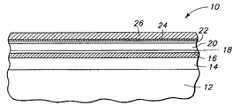
- a layer 18is formed over bottom electrode 16 .
- Layer 18can be referred to as a first layer of an assembly displaying differential negative resistance (such as a tunnel diode assembly), and can comprise Ge and one or more of S, Te and Se.
- layer 18will comprise, consist essentially of, or consist of Ge and Se.
- layer 18can comprise, consist essentially of, or consist of Ge x Se (1 ⁇ x) , such as, for example, Ge 0.4 Se 06 (also referred to as Ge 40 Se 60 ).
- Layer 18can be formed by, for example, either sputter deposition or evaporative deposition. If layer 18 is formed by sputter deposition, it can be formed from a target comprising both Ge and Se, and comprising the Ge and Se in a ratio which is identical to, or approximately, the desired ratio of the elements in layer 18 . Accordingly, if the desired ratio of Ge 40 Se 60 is to be formed in layer 18 , the layer can be sputter-deposited from a target comprising approximately 60 parts Se for every 40 parts Ge. The target can be a mosaic target.
- the layercan be formed by providing a source of Ge and a source of Se within a reaction chamber, and subsequently evaporating Ge and Se from the sources at appropriate rates to form the layer 18 having the desired stoichiometry of Ge and Se.
- layer 18is physically against bottom electrode 16 . It is to be understood, however, that optional intervening materials (not shown) can be provided between layers 16 and 18 .
- a layer 20is formed over layer 18 .
- Layer 20can be referred to as a second layer of a construction displaying differential negative resistance.
- Layer 20comprises M and A, where M is a transition metal and A is one or more of O, S, Te and Se.
- the M and Aare typically present in a stoichiometry of M (2+ ⁇ ) A, where ⁇ is greater than 0.
- the transition metal (M)can be, for example, a metal selected from Group IB of the periodic table (also referred to as Group 11 under the so-called new notation), and accordingly can be copper or silver, for example.
- second layer 20will comprise, consist essentially of, or consist of Ag (2+ ⁇ ) A, or Cu (2+ ⁇ ) A, where A is O, S, Te, and/or Se.
- Layer 20can be formed by, for example, either sputter deposition or evaporative deposition. In the shown aspect of the invention, layer 20 is physically against an upper surface of layer 18 .
- Layer 20can be formed by directly depositing a layer comprising M (2+ ⁇ ) A, or by depositing a layer which is subsequently converted to M (2+ ⁇ ) A. For instance, layer 20 can be formed by initially depositing a layer of Ag 2 Se, and subsequently diffusing additional Ag into the layer from regions proximate the layer to convert the layer to Ag (2+ ⁇ ) Se.
- a layer 22is formed over layer 20 .
- Layer 22can be referred to as a third layer of an assembly displaying differential negative resistance, and can comprise the same materials described previously for first layer 18 . Accordingly, layer 22 can comprise, consist essentially of, or consist of Ge and one or more of S, Te and Se. Layer 22 can be formed by, for example, either sputter deposition or evaporative deposition. In the shown aspect of the invention, layer 22 is physically against an upper surface of second layer 20 .
- Layer 24is formed over layer 22 .
- Layer 24can comprise the same metal (M) as is utilized in layer 20 .
- layer 24can comprise a different metal than is utilized in layer 20 .
- layer 24will comprise, consist essentially of, or consist of one or more transition elements.
- layer 24will comprise, consist essentially of, or consist of silver.
- Layer 24is typically very thin, and can comprise, for example, a thickness less than 300 angstroms, and in particular applications a thickness less than 50 angstroms.
- Conductive material 24is physically against an upper surface of material 22 in the shown aspect of the invention.
- Conductive material 26is formed over layer 24 .
- Conductive material 26can be referred to as a top electrode of an assembly displaying differential negative resistance.
- Conductive material 26can comprise identical materials as described above for incorporation into conductive material 16 . Accordingly, bottom electrode 16 and top electrode 26 can comprise identical compositions as one another. Alternatively, top electrode 26 can comprise a different chemical composition than does bottom electrode 16 . In particular applications, top electrode 26 will comprise, consist essentially of, or consist of one or both of tungsten and silver.
- top electrode 26is physically against conductive material 24 . If material 26 and conductive layer 24 both comprise silver, the top electrode 26 can be formed in a separate processing step from silver-containing layer 24 . Further, top electrode 26 can comprise a different silver composition than does layer 24 . Specifically, layer 24 can consist of very pure silver, whereas layer 26 can comprise a sliver alloy, such, for example, a copper/silver alloy. If top electrode 26 comprises silver, it can be advantageous to omit thin layer 24 from the construction 10 of FIG. 2 .
- layers 18 and 22can be electrically insulative, and can be referred to as glass layers. Further, layers 18 and 22 can be significantly thinner than the layer 20 provided between layers 18 and 22 . For instance, layers 18 and 22 can each be thinner than layer 20 by at least about 300 angstroms. In an exemplary application, layers 18 and 20 can each have thicknesses of at least about 150 angstroms, and the layer 20 can have a thickness of at least about 450 angstroms. In a specific application, layers 18 and 22 can each have thicknesses of about 150 angstroms, and layer 20 can have a thickness of about 470 angstroms.
- construction 30layers 16 , 18 , 20 , 22 , 24 and 26 are patterned into a construction 30 .
- Such patterningcan be accomplished by, for example, photolithographic processing utilized in conjunction with an appropriate etch, or series of etches, for extending a desired pattern through layers 16 , 18 , 20 , 22 , 24 and 26 .
- construction 30can correspond to a tunnel diode construction.
- Construction 30is shown electrically connected with potentials 32 and 34 through top and bottom electrodes 16 and 26 , respectively.
- Potential 32is positive relative to potential 34 , as indicated by the “+” and “ ⁇ ” symbols shown in FIG. 3 .
- Potentials 32 and 34can be utilized to drive current through construction 30 , and accordingly operate construction 30 as part of an integrated circuit assembly.
- Construction 30can be incorporated into the assembly as, for example, either a part of logic circuitry, or as part of a microwave oscillator construction.
- Potentials 32 and 34can be generated by other circuitry (not shown) associated with substrate 12 and incorporated within an integrated circuit comprising construction 30 .
- FIGS. 4-7Another aspect of the invention is described with reference to FIGS. 4-7 .
- similar numberingwill be utilized as was used above in describing the aspect of FIGS. 1-3 , where appropriate.
- Construction 50comprises substrate 12 , insulative material 14 , and bottom electrode 16 of the FIG. 1 construction.
- the construction 50can be formed in processing subsequent to that described above with reference to FIG. 1 , and accordingly can correspond to a processing stage subsequent to the stage of FIG. 1 .
- a material 52is formed over bottom electrode 16 .
- material 52is formed physically against bottom electrode 16 .
- Material 52comprises Ge and one or more of S, Te and Se.
- Material 52can comprise, for example, Ge x Se y , where “x” is from about 20 to about 30, and where “y” is from about 70 to about 80. The sum of x and y can be 100.
- Ge x Se ycan be expressed as comprising “x” from about 0.2 to about 0.3, “y” from about 0.7 to about 0.8, and “x”+“y” equal to 1.
- layer 52will comprise Ge 25 Se 75 .
- layer 52is formed physically against bottom electrode 16 .
- a conductive material 54is formed in a layer over material 52 .
- layer 54is formed physically against material 52 .
- Layer 54can comprise, consist essentially of, or consist of a transition metal.
- layer 54can comprise, consist essentially of, or consist of one or more transition metals selected from Group IB of the periodic table of the elements.
- layer 54can comprise, consist essentially of, or consist of copper or silver.
- material 52comprises Ge x Se y , where “x” is from about 20 to about 30, and where “y” is from about 70 to about 80; and layer 54 comprises, consists essentially of, or consists of silver.
- Layer 54can be formed to a thickness of, for example, about 100 ⁇ and layer 52 can be formed to a thickness of, for example, about 500 ⁇ .
- layer 54is exposed to light 56 having an appropriate energy to cause at least some of the metal from layer 54 to disperse within material 52 (with the dispersed metal being indicated by stippling throughout material 52 ).
- Light 56can comprise ultraviolet light.
- a suitable wavelength of light 56can be from about 200 nanometers to about 600 nanometers, which can disperse silver from layer 54 into material 52 .
- the amount of transition metal dispersed from layer 54 into material 52is preferably equal to or greater than an amount which saturates material 52 , but less than the amount which will crystallize separate phases of germanium-comprising constituents from within material 52 .
- material 52comprises Ge 25 Se 75
- layercomprises silver
- the amount of silver dispersed into material 52will preferably be sufficient to form phase-separated silver within the Ge/Se/Ag material 52 formed by dispersion of the silver into material 52 .
- the amount of silver dispersed into material 52will preferably be a low enough concentration to avoid crystallization of Ge/Se materials from within material 52 . If such crystallization occurs, such can break a potential within the material and impede or destroy operation of a tunnel diode (or other device displaying differential negative resistance) comprising the material.
- Material 52 and layer 54can be formed by either sputter deposition or evaporative deposition. It is noted that even though only some of the metal of layer 54 is shown dispersed into material 52 in the shown application, the invention can encompass other applications wherein an entirety of layer 54 , or substantially an entirety of the layer 54 , is dispersed into material 52 .
- Conductive material 26can be referred to as a top electrode, and can comprise identical components as described with reference to FIG. 2 for the material 26 of construction 10 . Accordingly, material 26 can comprise, consist essentially of, or consist of Ag, W, Ti, TiN, TaN and/or Pt; and in particular embodiments can comprise, consist essentially of, or consist of one or both of Ag and W. In the shown application, material 26 is formed physically against the layer 54 .
- layers 16 , 52 , 54 and 26are patterned into an assembly 60 .
- Such patterningcan be accomplished utilizing photolithographic processing and one or more suitable etches.
- the assembly 60can correspond to a tunnel diode assembly.
- the bottom electrode 16is electrically connected with a potential 32
- the top electrode 26is electrically connected with a potential 34 .
- the potential 32is positive relative to the potential 34 .
- Potentials 32 and 34can, as described above with reference to FIG. 3 , be part of an integrated circuit structure comprising assembly 60 .
- the construction 60can function comparably to the construction 30 of FIG. 3 . However, it may be more difficult to specifically tailor construction 60 for a particular desired operation than to tailor construction 30 . However, it can, in particular applications, be easier to accomplish the fabrication of construction 60 than that of construction 30 . Accordingly, both construction 60 and construction 30 can have advantages and disadvantages relative to one another.
- FIG. 8illustrates a graph of current (measured in microAmps) versus voltage (measured in Volts) for a device of the type described with reference to FIG. 3 , in which layers 18 and 22 comprise Ge 40 Se 60 , and in which layer 20 comprises Ag (2+ ⁇ ) Se, with ⁇ being greater than 0.
- the curve of FIG. 8demonstrates that the device has a first tunnel region (or DNR) 100 at a voltage slightly above ⁇ 0.5 Volts.
- the discrete quantum setsindicate that the Ag (2+ ⁇ ) Se of the device comprises at least about 20 quantized energy levels (the number of peaks in sets 102 and 104 , and which can also include the peak 100 ) when the layer is exposed to voltages having an absolute value of from 0 volts to 3.5 volts.
- the material having the quantized energy levelscan be considered to comprise, consist essentially of, or consist of Ag and Se.
- the number of quantized energy levelscan be considered to be, for example, at least 4, at least 6, at least 10, at least 15 and at least 20.
- the quantized energy levelscan, in particular aspects, be considered resonances (possibly discrete or separate relative to one another) induced when the material is exposed to appropriate voltages between 0 volts and ⁇ 3.5 volts (or, more generally, to appropriate voltages having an absolute value of from greater than 0 volts to 3.5 volts).
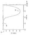
- the first tunnel region of a device formed in accordance with an aspect of the present inventionis shown on an expanded scale relative to the scale of FIG. 8 , in a graph 150 of current-versus-voltage.
- the deviceis described as having a peak ( 200 ) at about ⁇ 0.3 volts and a valley ( 202 ) at about ⁇ 0.6 volts. It is noted that the peak and valley are shown inverted in the graph of FIG. 9 , but convention would be to flip the graph so that the peak-to-valley ratio is greater than 1.
- the shown devicehas a peak-to-valley ratio of about ⁇ 50 microAmps/ ⁇ 0.4 microAmps, or in other words, about 130.
- the shown deviceis an exemplary device, and various other devices displaying differential negative resistance have been formed utilizing methodology of the present invention.
- Such deviceshave been found to have peak-to-valley ratios greater than 8, and specifically to have peak-to-valley ratios of at least 9, at least about 10, at least about 20, at least about 30, at least about 40, at least about 50, at least about 75, at least about 100, and greater than at least about 100 as demonstrated by FIG. 9 . It is found that the peak-to-valley ratios of devices of the present invention typically do not vary significantly with temperature, and specifically that the ratios stay relatively constant across a temperature range of from about ⁇ 30° C. to about 100° C.
- the device of FIG. 9has both the peak in current value ( 200 ) and the valley in current value ( 202 ) occurring within a voltage range of from less than 0 volts to greater than ⁇ 1 volt, or in other words, occurring within a voltage range having an absolute value of from greater than 0 volt to less than 1 volt.
- the assemblies of the present inventioncan have numerous applications, including, for example, applications in logic devices, and applications in microwave oscillator devices.
Landscapes
- Engineering & Computer Science (AREA)
- Manufacturing & Machinery (AREA)
- Semiconductor Memories (AREA)
Abstract
Description
- The invention pertains to semiconductor constructions, such as, for example, assemblies displaying differential negative resistance. The invention also pertains to methods of forming assemblies displaying differential negative resistance. In particular aspects, the assemblies displaying differential negative resistance are tunnel diode assemblies.
- Assemblies displaying differential negative resistance, such as tunnel diode assemblies, can be used as components in various types of circuits, including, for example, logic circuits, and microwave oscillators. It can therefore be desired to incorporate assemblies displaying differential negative resistance into integrated circuit structures.
- Various devices can be characterized in terms of the current passing through the devices relative to the amount of voltage applied to the devices. Some devices, such as, for example, tunnel diodes, will have an operating region in which an ohmic relationship of current as a function of voltage breaks down, and where a tunneling effect begins. A plot of current-versus-voltage for the devices will have a region referred to as the differential negative resistance (DNR) region, characterized by a non-ohmic relationship of current to voltage, and comprising a maximum in current value (typically referred to as a peak current value), and a minimum in current value (typically referred to as a valley current value).
- The ratio of the current at the peak to the current at the valley can be utilized as a figure-of-merit for a device displaying differential negative resistance. Higher peak-to-valley ratios are considered to indicate better-quality devices. Presently, the highest peak-to-valley ratios obtained for integrated circuit tunnel diode devices are less than 8. It would be desirable to develop better devices displaying differential negative resistance which can be incorporated into integrated circuits.
- It would also be desirable to develop methodology for incorporating such devices into integrated circuit constructions.
- In one aspect, the invention pertains to a device displaying differential negative resistance characterized by a current-versus-voltage profile having a peak-to-valley ratio of at least about 9.
- In one aspect, the invention pertains to a semiconductor construction comprising a substrate, and a first layer over the substrate. The first layer comprises Ge and one or more of S, Te and Se. A second layer is over the first layer. The second layer comprises M and A, where M is a transition metal and A is one or more of O, S, Te and Se. A third layer is over the second layer, and comprises Ge and one or more of S, Te and Se. The first, second and third layers are together incorporated into an assembly displaying differential negative resistance.
- In one aspect, the invention encompasses a semiconductor construction which includes a substrate and an assembly displaying differential negative resistance supported by the substrate. The assembly comprises a material which includes Ge, a transition metal, and one or more of S, Te and Se.
- The invention also encompasses methodology for forming the constructions and structures described above.
- Preferred embodiments of the invention are described below with reference to the following accompanying drawings.
FIG. 1 is a diagrammatic, cross-sectional view of a semiconductor wafer fragment at a preliminary processing stage in accordance with an aspect of the present invention.FIG. 2 is a view of theFIG. 1 fragment shown at a processing stage subsequent to that ofFIG. 1 .FIG. 3 is a view of theFIG. 1 fragment shown at a processing stage subsequent to that ofFIG. 2 .FIG. 4 is a view of a semiconductor wafer fragment shown at a processing stage subsequent to that ofFIG. 1 , and in accordance with a second aspect of the invention.FIG. 5 is a view of theFIG. 4 fragment shown at a processing stage subsequent to that ofFIG. 4 .FIG. 6 is a view of theFIG. 4 fragment shown at a processing stage subsequent to that ofFIG. 5 .FIG. 7 is a view of theFIG. 4 fragment shown at a processing stage subsequent to that ofFIG. 6 .FIG. 8 is a graph of current-versus-voltage for an exemplary device displaying differential negative resistance formed in accordance with an aspect of the present invention.FIG. 9 is a graph of current-versus-voltage for the so-called first tunnel region of an exemplary device displaying differential negative resistance formed in accordance with an aspect of the present invention.- A first aspect of the invention is described with reference to
FIGS. 1-3 . Referring initially toFIG. 1 , asemiconductor fragment 10 is illustrated at a preliminary processing stage.Fragment 10 comprises asubstrate 12.Substrate 12 can comprise, for example, monocrystalline silicon. To aid in interpretation of the claims that follow, the terms “semiconductive substrate” and “semiconductor substrate” are defined to mean any construction comprising semiconductive material, including, but not limited to, bulk semiconductive materials such as a semiconductive wafer (either alone or in assemblies comprising other materials thereon), and semiconductive material layers (either alone or in assemblies comprising other materials). The term “substrate” refers to any supporting structure, including, but not limited to, the semiconductive substrates described above. - A
layer 14 is formed oversubstrate 12.Layer 14 is an optional insulative material, and can comprise, for example, silicon dioxide, silicon nitride, borophosphosilicate glass (BPSG), and/or other insulative materials. Additionally, various conductive structures (not shown) can extend into or throughinsulative material 14. Such conductive structures can comprise part of an integrated circuit supported bysemiconductor substrate 12. - A
conductive material 16 is formed overinsulative material 14.Conductive material 16 can comprise, for example, various metals, such as, for example, one or more of silver, tungsten, titanium and platinum. In particular aspects,conductive material 16 can comprise titanium nitride, either alone, or in conjunction with one or more metals and/or metal alloys. Accordingly, conductive16 can comprise, consist essentially of, or consist of one or more of Ag, W, Ti, TiN and Pt. Additionally,layer 16 can comprise a conductively-doped semiconductive material.Layer 16 can be referred to as a bottom electrode in the discussion that follows. - Referring to
FIG. 2 , alayer 18 is formed overbottom electrode 16.Layer 18 can be referred to as a first layer of an assembly displaying differential negative resistance (such as a tunnel diode assembly), and can comprise Ge and one or more of S, Te and Se. - In particular applications,
layer 18 will comprise, consist essentially of, or consist of Ge and Se. For instance,layer 18 can comprise, consist essentially of, or consist of GexSe(1−x), such as, for example, Ge0.4Se06(also referred to as Ge40Se60). Layer 18 can be formed by, for example, either sputter deposition or evaporative deposition. Iflayer 18 is formed by sputter deposition, it can be formed from a target comprising both Ge and Se, and comprising the Ge and Se in a ratio which is identical to, or approximately, the desired ratio of the elements inlayer 18. Accordingly, if the desired ratio of Ge40Se60is to be formed inlayer 18, the layer can be sputter-deposited from a target comprising approximately 60 parts Se for every 40 parts Ge. The target can be a mosaic target.- If
layer 18 is formed by evaporative deposition, the layer can be formed by providing a source of Ge and a source of Se within a reaction chamber, and subsequently evaporating Ge and Se from the sources at appropriate rates to form thelayer 18 having the desired stoichiometry of Ge and Se. - In the shown embodiment,
layer 18 is physically againstbottom electrode 16. It is to be understood, however, that optional intervening materials (not shown) can be provided betweenlayers - A
layer 20 is formed overlayer 18.Layer 20 can be referred to as a second layer of a construction displaying differential negative resistance.Layer 20 comprises M and A, where M is a transition metal and A is one or more of O, S, Te and Se. The M and A are typically present in a stoichiometry of M(2+Δ)A, where Δ is greater than 0. The transition metal (M) can be, for example, a metal selected from Group IB of the periodic table (also referred to as Group 11 under the so-called new notation), and accordingly can be copper or silver, for example. In particular embodiments,second layer 20 will comprise, consist essentially of, or consist of Ag(2+Δ)A, or Cu(2+Δ)A, where A is O, S, Te, and/or Se. Layer 20 can be formed by, for example, either sputter deposition or evaporative deposition. In the shown aspect of the invention,layer 20 is physically against an upper surface oflayer 18.Layer 20 can be formed by directly depositing a layer comprising M(2+Δ)A, or by depositing a layer which is subsequently converted to M(2+Δ)A. For instance,layer 20 can be formed by initially depositing a layer of Ag2Se, and subsequently diffusing additional Ag into the layer from regions proximate the layer to convert the layer to Ag(2+Δ)Se.- A
layer 22 is formed overlayer 20.Layer 22 can be referred to as a third layer of an assembly displaying differential negative resistance, and can comprise the same materials described previously forfirst layer 18. Accordingly,layer 22 can comprise, consist essentially of, or consist of Ge and one or more of S, Te and Se.Layer 22 can be formed by, for example, either sputter deposition or evaporative deposition. In the shown aspect of the invention,layer 22 is physically against an upper surface ofsecond layer 20. - An electrically
conductive layer 24 is formed overlayer 22.Layer 24 can comprise the same metal (M) as is utilized inlayer 20. Alternatively,layer 24 can comprise a different metal than is utilized inlayer 20. In particular applications,layer 24 will comprise, consist essentially of, or consist of one or more transition elements. In an exemplary application,layer 24 will comprise, consist essentially of, or consist of silver.Layer 24 is typically very thin, and can comprise, for example, a thickness less than 300 angstroms, and in particular applications a thickness less than 50 angstroms.Conductive material 24 is physically against an upper surface ofmaterial 22 in the shown aspect of the invention. - A
conductive material 26 is formed overlayer 24.Conductive material 26 can be referred to as a top electrode of an assembly displaying differential negative resistance.Conductive material 26 can comprise identical materials as described above for incorporation intoconductive material 16. Accordingly,bottom electrode 16 andtop electrode 26 can comprise identical compositions as one another. Alternatively,top electrode 26 can comprise a different chemical composition than doesbottom electrode 16. In particular applications,top electrode 26 will comprise, consist essentially of, or consist of one or both of tungsten and silver. - In the shown application,
top electrode 26 is physically againstconductive material 24. Ifmaterial 26 andconductive layer 24 both comprise silver, thetop electrode 26 can be formed in a separate processing step from silver-containinglayer 24. Further,top electrode 26 can comprise a different silver composition than does layer24. Specifically,layer 24 can consist of very pure silver, whereaslayer 26 can comprise a sliver alloy, such, for example, a copper/silver alloy. Iftop electrode 26 comprises silver, it can be advantageous to omitthin layer 24 from theconstruction 10 ofFIG. 2 . - In the
construction 10 ofFIG. 2 , layers18 and22 can be electrically insulative, and can be referred to as glass layers. Further, layers18 and22 can be significantly thinner than thelayer 20 provided betweenlayers layer 20 by at least about 300 angstroms. In an exemplary application, layers18 and20 can each have thicknesses of at least about 150 angstroms, and thelayer 20 can have a thickness of at least about 450 angstroms. In a specific application, layers18 and22 can each have thicknesses of about 150 angstroms, andlayer 20 can have a thickness of about 470 angstroms. - Referring to
FIG. 3 , layers16,18,20,22,24 and26 are patterned into aconstruction 30. Such patterning can be accomplished by, for example, photolithographic processing utilized in conjunction with an appropriate etch, or series of etches, for extending a desired pattern throughlayers construction 30 can correspond to a tunnel diode construction. Construction 30 is shown electrically connected withpotentials bottom electrodes Potential 32 is positive relative to potential34, as indicated by the “+” and “−” symbols shown inFIG. 3 .Potentials construction 30, and accordingly operateconstruction 30 as part of an integrated circuit assembly.Construction 30 can be incorporated into the assembly as, for example, either a part of logic circuitry, or as part of a microwave oscillator construction.Potentials substrate 12 and incorporated within an integratedcircuit comprising construction 30.- Another aspect of the invention is described with reference to
FIGS. 4-7 . In referring toFIGS. 4-7 , similar numbering will be utilized as was used above in describing the aspect ofFIGS. 1-3 , where appropriate. - Referring initially to
FIG. 4 , aconstruction 50 is illustrated at a preliminary stage of the second aspect of the invention.Construction 50 comprisessubstrate 12,insulative material 14, andbottom electrode 16 of theFIG. 1 construction. Theconstruction 50 can be formed in processing subsequent to that described above with reference toFIG. 1 , and accordingly can correspond to a processing stage subsequent to the stage ofFIG. 1 . - A
material 52 is formed overbottom electrode 16. In the shown embodiment,material 52 is formed physically againstbottom electrode 16.Material 52 comprises Ge and one or more of S, Te and Se.Material 52 can comprise, for example, GexSey, where “x” is from about 20 to about 30, and where “y” is from about 70 to about 80. The sum of x and y can be 100. Alternatively, GexSey, can be expressed as comprising “x” from about 0.2 to about 0.3, “y” from about 0.7 to about 0.8, and “x”+“y” equal to 1. - In particular applications,
layer 52 will comprise Ge25Se75. In the shown application,layer 52 is formed physically againstbottom electrode 16. - A
conductive material 54 is formed in a layer overmaterial 52. In the shown application,layer 54 is formed physically againstmaterial 52.Layer 54 can comprise, consist essentially of, or consist of a transition metal. In particular applications,layer 54 can comprise, consist essentially of, or consist of one or more transition metals selected from Group IB of the periodic table of the elements. For instance,layer 54 can comprise, consist essentially of, or consist of copper or silver. In an exemplary application,material 52 comprises GexSey, where “x” is from about 20 to about 30, and where “y” is from about 70 to about 80; andlayer 54 comprises, consists essentially of, or consists of silver.Layer 54 can be formed to a thickness of, for example, about 100 Å andlayer 52 can be formed to a thickness of, for example, about 500 Å. - Referring to
FIG. 5 ,layer 54 is exposed to light56 having an appropriate energy to cause at least some of the metal fromlayer 54 to disperse within material52 (with the dispersed metal being indicated by stippling throughout material52).Light 56 can comprise ultraviolet light. In an exemplary application a suitable wavelength of light56 can be from about 200 nanometers to about 600 nanometers, which can disperse silver fromlayer 54 intomaterial 52. - The amount of transition metal dispersed from
layer 54 intomaterial 52 is preferably equal to or greater than an amount which saturatesmaterial 52, but less than the amount which will crystallize separate phases of germanium-comprising constituents from withinmaterial 52. For instance, ifmaterial 52 comprises Ge25Se75, and layer comprises silver, the amount of silver dispersed intomaterial 52 will preferably be sufficient to form phase-separated silver within the Ge/Se/Ag material 52 formed by dispersion of the silver intomaterial 52. However, the amount of silver dispersed intomaterial 52 will preferably be a low enough concentration to avoid crystallization of Ge/Se materials from withinmaterial 52. If such crystallization occurs, such can break a potential within the material and impede or destroy operation of a tunnel diode (or other device displaying differential negative resistance) comprising the material. Material 52 andlayer 54 can be formed by either sputter deposition or evaporative deposition. It is noted that even though only some of the metal oflayer 54 is shown dispersed intomaterial 52 in the shown application, the invention can encompass other applications wherein an entirety oflayer 54, or substantially an entirety of thelayer 54, is dispersed intomaterial 52.- Referring to
FIG. 6 , aconductive material 26 is formed overlayer 54.Conductive material 26 can be referred to as a top electrode, and can comprise identical components as described with reference toFIG. 2 for thematerial 26 ofconstruction 10. Accordingly,material 26 can comprise, consist essentially of, or consist of Ag, W, Ti, TiN, TaN and/or Pt; and in particular embodiments can comprise, consist essentially of, or consist of one or both of Ag and W. In the shown application,material 26 is formed physically against thelayer 54. - Referring to
FIG. 7 , layers16,52,54 and26 are patterned into anassembly 60. Such patterning can be accomplished utilizing photolithographic processing and one or more suitable etches. Theassembly 60 can correspond to a tunnel diode assembly. - The
bottom electrode 16 is electrically connected with a potential32, and thetop electrode 26 is electrically connected with a potential34. The potential32 is positive relative to the potential34.Potentials FIG. 3 , be part of an integrated circuitstructure comprising assembly 60. - The
construction 60 can function comparably to theconstruction 30 ofFIG. 3 . However, it may be more difficult to specifically tailorconstruction 60 for a particular desired operation than to tailorconstruction 30. However, it can, in particular applications, be easier to accomplish the fabrication ofconstruction 60 than that ofconstruction 30. Accordingly, bothconstruction 60 andconstruction 30 can have advantages and disadvantages relative to one another. - The devices displaying differential negative resistance displaying differential negative resistance formed in accordance with aspects of the present invention can have exceptional operating characteristics. Such characteristics are described with reference to
FIGS. 8 and 9 .FIG. 8 illustrates a graph of current (measured in microAmps) versus voltage (measured in Volts) for a device of the type described with reference toFIG. 3 , in which layers18 and22 comprise Ge40Se60, and in whichlayer 20 comprises Ag(2+Δ)Se, with Δ being greater than 0. The curve ofFIG. 8 demonstrates that the device has a first tunnel region (or DNR)100 at a voltage slightly above −0.5 Volts.FIG. 8 also shows that discreet quantum sets (illustrated generally byarrows 102 and104) occur at about −2.0 Volts and at about −3.0 Volts. The discrete quantum sets indicate that the Ag(2+Δ)Se of the device comprises at least about 20 quantized energy levels (the number of peaks insets - Referring to
FIG. 9 , the first tunnel region of a device formed in accordance with an aspect of the present invention is shown on an expanded scale relative to the scale ofFIG. 8 , in agraph 150 of current-versus-voltage. In accordance with convention, the device is described as having a peak (200) at about −0.3 volts and a valley (202) at about −0.6 volts. It is noted that the peak and valley are shown inverted in the graph ofFIG. 9 , but convention would be to flip the graph so that the peak-to-valley ratio is greater than 1. The shown device has a peak-to-valley ratio of about −50 microAmps/−0.4 microAmps, or in other words, about 130. The shown device is an exemplary device, and various other devices displaying differential negative resistance have been formed utilizing methodology of the present invention. Such devices have been found to have peak-to-valley ratios greater than 8, and specifically to have peak-to-valley ratios of at least 9, at least about 10, at least about 20, at least about 30, at least about 40, at least about 50, at least about 75, at least about 100, and greater than at least about 100 as demonstrated byFIG. 9 . It is found that the peak-to-valley ratios of devices of the present invention typically do not vary significantly with temperature, and specifically that the ratios stay relatively constant across a temperature range of from about −30° C. to about 100° C. - The device of
FIG. 9 has both the peak in current value (200) and the valley in current value (202) occurring within a voltage range of from less than 0 volts to greater than −1 volt, or in other words, occurring within a voltage range having an absolute value of from greater than 0 volt to less than 1 volt. - The assemblies of the present invention can have numerous applications, including, for example, applications in logic devices, and applications in microwave oscillator devices.
- In compliance with the statute, the invention has been described in language more or less specific as to structural and methodical features. It is to be understood, however, that the invention is not limited to the specific features shown and described, since the means herein disclosed comprise preferred forms of putting the invention into effect. The invention is, therefore, claimed in any of its forms or modifications within the proper scope of the appended claims appropriately interpreted in accordance with the doctrine of equivalents.
Claims (27)
Priority Applications (1)
| Application Number | Priority Date | Filing Date | Title |
|---|---|---|---|
| US12/068,020US7879646B2 (en) | 2002-07-10 | 2008-01-31 | Assemblies displaying differential negative resistance, semiconductor constructions, and methods of forming assemblies displaying differential negative resistance |
Applications Claiming Priority (3)
| Application Number | Priority Date | Filing Date | Title |
|---|---|---|---|
| US10/193,529US7015494B2 (en) | 2002-07-10 | 2002-07-10 | Assemblies displaying differential negative resistance |
| US11/181,879US7387909B2 (en) | 2002-07-10 | 2005-07-15 | Methods of forming assemblies displaying differential negative resistance |
| US12/068,020US7879646B2 (en) | 2002-07-10 | 2008-01-31 | Assemblies displaying differential negative resistance, semiconductor constructions, and methods of forming assemblies displaying differential negative resistance |
Related Parent Applications (1)
| Application Number | Title | Priority Date | Filing Date |
|---|---|---|---|
| US11/181,879ContinuationUS7387909B2 (en) | 2002-07-10 | 2005-07-15 | Methods of forming assemblies displaying differential negative resistance |
Publications (2)
| Publication Number | Publication Date |
|---|---|
| US20080188034A1true US20080188034A1 (en) | 2008-08-07 |
| US7879646B2 US7879646B2 (en) | 2011-02-01 |
Family
ID=30114545
Family Applications (4)
| Application Number | Title | Priority Date | Filing Date |
|---|---|---|---|
| US10/193,529Expired - Fee RelatedUS7015494B2 (en) | 2002-07-10 | 2002-07-10 | Assemblies displaying differential negative resistance |
| US11/180,692AbandonedUS20050247927A1 (en) | 2002-07-10 | 2005-07-14 | Assemblies displaying differential negative resistance |
| US11/181,879Expired - LifetimeUS7387909B2 (en) | 2002-07-10 | 2005-07-15 | Methods of forming assemblies displaying differential negative resistance |
| US12/068,020Expired - Fee RelatedUS7879646B2 (en) | 2002-07-10 | 2008-01-31 | Assemblies displaying differential negative resistance, semiconductor constructions, and methods of forming assemblies displaying differential negative resistance |
Family Applications Before (3)
| Application Number | Title | Priority Date | Filing Date |
|---|---|---|---|
| US10/193,529Expired - Fee RelatedUS7015494B2 (en) | 2002-07-10 | 2002-07-10 | Assemblies displaying differential negative resistance |
| US11/180,692AbandonedUS20050247927A1 (en) | 2002-07-10 | 2005-07-14 | Assemblies displaying differential negative resistance |
| US11/181,879Expired - LifetimeUS7387909B2 (en) | 2002-07-10 | 2005-07-15 | Methods of forming assemblies displaying differential negative resistance |
Country Status (1)
| Country | Link |
|---|---|
| US (4) | US7015494B2 (en) |
Cited By (5)
| Publication number | Priority date | Publication date | Assignee | Title |
|---|---|---|---|---|
| US20080121859A1 (en)* | 2006-10-19 | 2008-05-29 | Boise State University | Forced ion migration for chalcogenide phase change memory device |
| US20100027324A1 (en)* | 2008-08-01 | 2010-02-04 | Boise State University | Variable integrated analog resistor |
| US20110079709A1 (en)* | 2009-10-07 | 2011-04-07 | Campbell Kristy A | Wide band sensor |
| US8284590B2 (en) | 2010-05-06 | 2012-10-09 | Boise State University | Integratable programmable capacitive device |
| US8467236B2 (en) | 2008-08-01 | 2013-06-18 | Boise State University | Continuously variable resistor |
Families Citing this family (12)
| Publication number | Priority date | Publication date | Assignee | Title |
|---|---|---|---|---|
| US7364644B2 (en)* | 2002-08-29 | 2008-04-29 | Micron Technology, Inc. | Silver selenide film stoichiometry and morphology control in sputter deposition |
| US7190048B2 (en)* | 2004-07-19 | 2007-03-13 | Micron Technology, Inc. | Resistance variable memory device and method of fabrication |
| JP4830275B2 (en)* | 2004-07-22 | 2011-12-07 | ソニー株式会社 | Memory element |
| US7505309B2 (en)* | 2005-04-20 | 2009-03-17 | Micron Technology, Inc. | Static RAM memory cell with DNR chalcogenide devices and method of forming |
| US7166520B1 (en)* | 2005-08-08 | 2007-01-23 | Silicon Genesis Corporation | Thin handle substrate method and structure for fabricating devices using one or more films provided by a layer transfer process |
| KR101102157B1 (en)* | 2005-09-16 | 2012-01-02 | 삼성전자주식회사 | Volatile Negative Resistance Device Using Metal Nanoparticles |
| US8154003B2 (en) | 2007-08-09 | 2012-04-10 | Taiwan Semiconductor Manufacturing Company, Ltd. | Resistive non-volatile memory device |
| JP4466738B2 (en)* | 2008-01-09 | 2010-05-26 | ソニー株式会社 | Storage element and storage device |
| US8419176B2 (en) | 2009-05-29 | 2013-04-16 | Eastman Kodak Company | Aqueous compositions with improved silicon corrosion characteristics |
| US20130237661A1 (en) | 2011-12-22 | 2013-09-12 | Thomas B. Brust | Inkjet ink composition |
| US9583699B2 (en) | 2015-06-01 | 2017-02-28 | Boise State University | Tunable variable resistance memory device |
| US9583703B2 (en) | 2015-06-01 | 2017-02-28 | Boise State University | Tunable variable resistance memory device |
Citations (89)
| Publication number | Priority date | Publication date | Assignee | Title |
|---|---|---|---|---|
| US3743847A (en)* | 1971-06-01 | 1973-07-03 | Motorola Inc | Amorphous silicon film as a uv filter |
| US3961314A (en)* | 1974-03-05 | 1976-06-01 | Energy Conversion Devices, Inc. | Structure and method for producing an image |
| US3966317A (en)* | 1974-04-08 | 1976-06-29 | Energy Conversion Devices, Inc. | Dry process production of archival microform records from hard copy |
| US4267261A (en)* | 1971-07-15 | 1981-05-12 | Energy Conversion Devices, Inc. | Method for full format imaging |
| US4269935A (en)* | 1979-07-13 | 1981-05-26 | Ionomet Company, Inc. | Process of doping silver image in chalcogenide layer |
| US4312938A (en)* | 1979-07-06 | 1982-01-26 | Drexler Technology Corporation | Method for making a broadband reflective laser recording and data storage medium with absorptive underlayer |
| US4320191A (en)* | 1978-11-07 | 1982-03-16 | Nippon Telegraph & Telephone Public Corporation | Pattern-forming process |
| US4499557A (en)* | 1980-10-28 | 1985-02-12 | Energy Conversion Devices, Inc. | Programmable cell for use in programmable electronic arrays |
| US4597162A (en)* | 1983-01-18 | 1986-07-01 | Energy Conversion Devices, Inc. | Method for making, parallel preprogramming or field programming of electronic matrix arrays |
| US4608296A (en)* | 1983-12-06 | 1986-08-26 | Energy Conversion Devices, Inc. | Superconducting films and devices exhibiting AC to DC conversion |
| US4637895A (en)* | 1985-04-01 | 1987-01-20 | Energy Conversion Devices, Inc. | Gas mixtures for the vapor deposition of semiconductor material |
| US4646266A (en)* | 1984-09-28 | 1987-02-24 | Energy Conversion Devices, Inc. | Programmable semiconductor structures and methods for using the same |
| US4664939A (en)* | 1985-04-01 | 1987-05-12 | Energy Conversion Devices, Inc. | Vertical semiconductor processor |
| US4668968A (en)* | 1984-05-14 | 1987-05-26 | Energy Conversion Devices, Inc. | Integrated circuit compatible thin film field effect transistor and method of making same |
| US4670763A (en)* | 1984-05-14 | 1987-06-02 | Energy Conversion Devices, Inc. | Thin film field effect transistor |
| US4673957A (en)* | 1984-05-14 | 1987-06-16 | Energy Conversion Devices, Inc. | Integrated circuit compatible thin film field effect transistor and method of making same |
| US4678679A (en)* | 1984-06-25 | 1987-07-07 | Energy Conversion Devices, Inc. | Continuous deposition of activated process gases |
| US4728406A (en)* | 1986-08-18 | 1988-03-01 | Energy Conversion Devices, Inc. | Method for plasma - coating a semiconductor body |
| US4737379A (en)* | 1982-09-24 | 1988-04-12 | Energy Conversion Devices, Inc. | Plasma deposited coatings, and low temperature plasma method of making same |
| US4795557A (en)* | 1986-06-18 | 1989-01-03 | Otv (Omnium De Traitements Et De Valorisation) | Apparatus for gas transfer and flotation for treating water to be purified |
| US4809044A (en)* | 1986-08-22 | 1989-02-28 | Energy Conversion Devices, Inc. | Thin film overvoltage protection devices |
| US4818717A (en)* | 1986-06-27 | 1989-04-04 | Energy Conversion Devices, Inc. | Method for making electronic matrix arrays |
| US4843443A (en)* | 1984-05-14 | 1989-06-27 | Energy Conversion Devices, Inc. | Thin film field effect transistor and method of making same |
| US4845533A (en)* | 1986-08-22 | 1989-07-04 | Energy Conversion Devices, Inc. | Thin film electrical devices with amorphous carbon electrodes and method of making same |
| US4847674A (en)* | 1987-03-10 | 1989-07-11 | Advanced Micro Devices, Inc. | High speed interconnect system with refractory non-dogbone contacts and an active electromigration suppression mechanism |
| US4891330A (en)* | 1987-07-27 | 1990-01-02 | Energy Conversion Devices, Inc. | Method of fabricating n-type and p-type microcrystalline semiconductor alloy material including band gap widening elements |
| US5128099A (en)* | 1991-02-15 | 1992-07-07 | Energy Conversion Devices, Inc. | Congruent state changeable optical memory material and device |
| US5177567A (en)* | 1991-07-19 | 1993-01-05 | Energy Conversion Devices, Inc. | Thin-film structure for chalcogenide electrical switching devices and process therefor |
| US5219788A (en)* | 1991-02-25 | 1993-06-15 | Ibm Corporation | Bilayer metallization cap for photolithography |
| US5296716A (en)* | 1991-01-18 | 1994-03-22 | Energy Conversion Devices, Inc. | Electrically erasable, directly overwritable, multibit single cell memory elements and arrays fabricated therefrom |
| US5315131A (en)* | 1990-11-22 | 1994-05-24 | Matsushita Electric Industrial Co., Ltd. | Electrically reprogrammable nonvolatile memory device |
| US5406509A (en)* | 1991-01-18 | 1995-04-11 | Energy Conversion Devices, Inc. | Electrically erasable, directly overwritable, multibit single cell memory elements and arrays fabricated therefrom |
| US5414271A (en)* | 1991-01-18 | 1995-05-09 | Energy Conversion Devices, Inc. | Electrically erasable memory elements having improved set resistance stability |
| US5500532A (en)* | 1994-08-18 | 1996-03-19 | Arizona Board Of Regents | Personal electronic dosimeter |
| US5512328A (en)* | 1992-08-07 | 1996-04-30 | Hitachi, Ltd. | Method for forming a pattern and forming a thin film used in pattern formation |
| US5512773A (en)* | 1993-12-23 | 1996-04-30 | U.S. Philips Corporation | Switching element with memory provided with Schottky tunnelling barrier |
| US5534712A (en)* | 1991-01-18 | 1996-07-09 | Energy Conversion Devices, Inc. | Electrically erasable memory elements characterized by reduced current and improved thermal stability |
| US5534711A (en)* | 1991-01-18 | 1996-07-09 | Energy Conversion Devices, Inc. | Electrically erasable, directly overwritable, multibit single cell memory elements and arrays fabricated therefrom |
| US5536947A (en)* | 1991-01-18 | 1996-07-16 | Energy Conversion Devices, Inc. | Electrically erasable, directly overwritable, multibit single cell memory element and arrays fabricated therefrom |
| US5591501A (en)* | 1995-12-20 | 1997-01-07 | Energy Conversion Devices, Inc. | Optical recording medium having a plurality of discrete phase change data recording points |
| US5596522A (en)* | 1991-01-18 | 1997-01-21 | Energy Conversion Devices, Inc. | Homogeneous compositions of microcrystalline semiconductor material, semiconductor devices and directly overwritable memory elements fabricated therefrom, and arrays fabricated from the memory elements |
| US5714768A (en)* | 1995-10-24 | 1998-02-03 | Energy Conversion Devices, Inc. | Second-layer phase change memory array on top of a logic device |
| US5726083A (en)* | 1994-11-29 | 1998-03-10 | Nec Corporation | Process of fabricating dynamic random access memory device having storage capacitor low in contact resistance and small in leakage current through tantalum oxide film |
| US5751012A (en)* | 1995-06-07 | 1998-05-12 | Micron Technology, Inc. | Polysilicon pillar diode for use in a non-volatile memory cell |
| US5761115A (en)* | 1996-05-30 | 1998-06-02 | Axon Technologies Corporation | Programmable metallization cell structure and method of making same |
| US5912839A (en)* | 1998-06-23 | 1999-06-15 | Energy Conversion Devices, Inc. | Universal memory element and method of programming same |
| US5912104A (en)* | 1993-06-18 | 1999-06-15 | Hitachi, Ltd. | Information recording medium |
| US5920788A (en)* | 1995-06-07 | 1999-07-06 | Micron Technology, Inc. | Chalcogenide memory cell with a plurality of chalcogenide electrodes |
| US6011757A (en)* | 1998-01-27 | 2000-01-04 | Ovshinsky; Stanford R. | Optical recording media having increased erasability |
| US6077729A (en)* | 1995-06-07 | 2000-06-20 | Micron Technology, Inc. | Memory array having a multi-state element and method for forming such array or cellis thereof |
| US6087674A (en)* | 1996-10-28 | 2000-07-11 | Energy Conversion Devices, Inc. | Memory element with memory material comprising phase-change material and dielectric material |
| US6177338B1 (en)* | 1999-02-08 | 2001-01-23 | Taiwan Semiconductor Manufacturing Company | Two step barrier process |
| US6236059B1 (en)* | 1996-08-22 | 2001-05-22 | Micron Technology, Inc. | Memory cell incorporating a chalcogenide element and method of making same |
| US20020000666A1 (en)* | 1998-08-31 | 2002-01-03 | Michael N. Kozicki | Self-repairing interconnections for electrical circuits |
| US6339544B1 (en)* | 2000-09-29 | 2002-01-15 | Intel Corporation | Method to enhance performance of thermal resistor device |
| US6348365B1 (en)* | 2001-03-02 | 2002-02-19 | Micron Technology, Inc. | PCRAM cell manufacturing |
| US6350679B1 (en)* | 1999-08-03 | 2002-02-26 | Micron Technology, Inc. | Methods of providing an interlevel dielectric layer intermediate different elevation conductive metal layers in the fabrication of integrated circuitry |
| US6376284B1 (en)* | 1996-02-23 | 2002-04-23 | Micron Technology, Inc. | Method of fabricating a memory device |
| US6391688B1 (en)* | 1995-06-07 | 2002-05-21 | Micron Technology, Inc. | Method for fabricating an array of ultra-small pores for chalcogenide memory cells |
| US6404665B1 (en)* | 2000-09-29 | 2002-06-11 | Intel Corporation | Compositionally modified resistive electrode |
| US6414376B1 (en)* | 1997-07-31 | 2002-07-02 | Micron Technology, Inc. | Method and apparatus for reducing isolation stress in integrated circuits |
| US6418049B1 (en)* | 1997-12-04 | 2002-07-09 | Arizona Board Of Regents | Programmable sub-surface aggregating metallization structure and method of making same |
| US6423628B1 (en)* | 1999-10-22 | 2002-07-23 | Lsi Logic Corporation | Method of forming integrated circuit structure having low dielectric constant material and having silicon oxynitride caps over closely spaced apart metal lines |
| US6507061B1 (en)* | 2001-08-31 | 2003-01-14 | Intel Corporation | Multiple layer phase-change memory |
| US6511867B2 (en)* | 2001-06-30 | 2003-01-28 | Ovonyx, Inc. | Utilizing atomic layer deposition for programmable device |
| US6511862B2 (en)* | 2001-06-30 | 2003-01-28 | Ovonyx, Inc. | Modified contact for programmable devices |
| US6514805B2 (en)* | 2001-06-30 | 2003-02-04 | Intel Corporation | Trench sidewall profile for device isolation |
| US6531373B2 (en)* | 2000-12-27 | 2003-03-11 | Ovonyx, Inc. | Method of forming a phase-change memory cell using silicon on insulator low electrode in charcogenide elements |
| US20030048744A1 (en)* | 2001-09-01 | 2003-03-13 | Ovshinsky Stanford R. | Increased data storage in optical data storage and retrieval systems using blue lasers and/or plasmon lenses |
| US6534781B2 (en)* | 2000-12-26 | 2003-03-18 | Ovonyx, Inc. | Phase-change memory bipolar array utilizing a single shallow trench isolation for creating an individual active area region for two memory array elements and one bipolar base contact |
| US6545907B1 (en)* | 2001-10-30 | 2003-04-08 | Ovonyx, Inc. | Technique and apparatus for performing write operations to a phase change material memory device |
| US6545287B2 (en)* | 2001-09-07 | 2003-04-08 | Intel Corporation | Using selective deposition to form phase-change memory cells |
| US6555860B2 (en)* | 2000-09-29 | 2003-04-29 | Intel Corporation | Compositionally modified resistive electrode |
| US6563164B2 (en)* | 2000-09-29 | 2003-05-13 | Ovonyx, Inc. | Compositionally modified resistive electrode |
| US6566700B2 (en)* | 2001-10-11 | 2003-05-20 | Ovonyx, Inc. | Carbon-containing interfacial layer for phase-change memory |
| US6567293B1 (en)* | 2000-09-29 | 2003-05-20 | Ovonyx, Inc. | Single level metal memory cell using chalcogenide cladding |
| US6570784B2 (en)* | 2001-06-29 | 2003-05-27 | Ovonyx, Inc. | Programming a phase-change material memory |
| US6569705B2 (en)* | 2000-12-21 | 2003-05-27 | Intel Corporation | Metal structure for a phase-change memory device |
| US6576921B2 (en)* | 2001-11-08 | 2003-06-10 | Intel Corporation | Isolating phase change material memory cells |
| US6586761B2 (en)* | 2001-09-07 | 2003-07-01 | Intel Corporation | Phase change material memory device |
| US6589714B2 (en)* | 2001-06-26 | 2003-07-08 | Ovonyx, Inc. | Method for making programmable resistance memory element using silylated photoresist |
| US6590807B2 (en)* | 2001-08-02 | 2003-07-08 | Intel Corporation | Method for reading a structural phase-change memory |
| US6597009B2 (en)* | 2000-09-29 | 2003-07-22 | Intel Corporation | Reduced contact area of sidewall conductor |
| US6673700B2 (en)* | 2001-06-30 | 2004-01-06 | Ovonyx, Inc. | Reduced area intersection between electrode and programming element |
| US6687427B2 (en)* | 2000-12-29 | 2004-02-03 | Intel Corporation | Optic switch |
| US6690026B2 (en)* | 2001-09-28 | 2004-02-10 | Intel Corporation | Method of fabricating a three-dimensional array of active media |
| US6696355B2 (en)* | 2000-12-14 | 2004-02-24 | Ovonyx, Inc. | Method to selectively increase the top resistance of the lower programming electrode in a phase-change memory |
| US20040035401A1 (en)* | 2002-08-26 | 2004-02-26 | Subramanian Ramachandran | Hydrogen powered scooter |
| US6714954B2 (en)* | 2002-05-10 | 2004-03-30 | Energy Conversion Devices, Inc. | Methods of factoring and modular arithmetic |
Family Cites Families (66)
| Publication number | Priority date | Publication date | Assignee | Title |
|---|---|---|---|---|
| US3271591A (en) | 1963-09-20 | 1966-09-06 | Energy Conversion Devices Inc | Symmetrical current controlling device |
| US3622319A (en) | 1966-10-20 | 1971-11-23 | Western Electric Co | Nonreflecting photomasks and methods of making same |
| US3626257A (en) | 1969-04-01 | 1971-12-07 | Ibm | Semiconductor device with superlattice region |
| US3868651A (en) | 1970-08-13 | 1975-02-25 | Energy Conversion Devices Inc | Method and apparatus for storing and reading data in a memory having catalytic material to initiate amorphous to crystalline change in memory structure |
| US4029520A (en)* | 1972-10-02 | 1977-06-14 | Minnesota Mining And Manufacturing Company | Thermoelectric generators that incorporate self-segmenting thermoelectric legs |
| US4177474A (en) | 1977-05-18 | 1979-12-04 | Energy Conversion Devices, Inc. | High temperature amorphous semiconductor member and method of making the same |
| DE2901303C2 (en) | 1979-01-15 | 1984-04-19 | Max Planck Gesellschaft Zur Foerderung Der Wissenschaften E.V., 3400 Goettingen | Solid ionic conductor material, its use and process for its manufacture |
| JPS6024580B2 (en) | 1980-03-10 | 1985-06-13 | 日本電信電話株式会社 | Manufacturing method for semiconductor devices |
| US4405710A (en) | 1981-06-22 | 1983-09-20 | Cornell Research Foundation, Inc. | Ion beam exposure of (g-Gex -Se1-x) inorganic resists |
| US4795657A (en)* | 1984-04-13 | 1989-01-03 | Energy Conversion Devices, Inc. | Method of fabricating a programmable array |
| US4769338A (en) | 1984-05-14 | 1988-09-06 | Energy Conversion Devices, Inc. | Thin film field effect transistor and method of making same |
| FR2580273B1 (en)* | 1985-03-25 | 1990-01-05 | Rhone Poulenc Spec Chim | PROCESS FOR SEPARATING CERIUM AND RARE EARTH |
| US4710899A (en) | 1985-06-10 | 1987-12-01 | Energy Conversion Devices, Inc. | Data storage medium incorporating a transition metal for increased switching speed |
| US4766471A (en)* | 1986-01-23 | 1988-08-23 | Energy Conversion Devices, Inc. | Thin film electro-optical devices |
| US4788594A (en) | 1986-10-15 | 1988-11-29 | Energy Conversion Devices, Inc. | Solid state electronic camera including thin film matrix of photosensors |
| US4853785A (en)* | 1986-10-15 | 1989-08-01 | Energy Conversion Devices, Inc. | Electronic camera including electronic signal storage cartridge |
| US4775425A (en) | 1987-07-27 | 1988-10-04 | Energy Conversion Devices, Inc. | P and n-type microcrystalline semiconductor alloy material including band gap widening elements, devices utilizing same |
| GB8910854D0 (en) | 1989-05-11 | 1989-06-28 | British Petroleum Co Plc | Semiconductor device |
| GB2239983A (en)* | 1989-12-22 | 1991-07-17 | Univ Southampton | Optical fibre laser |
| US5159661A (en) | 1990-10-05 | 1992-10-27 | Energy Conversion Devices, Inc. | Vertically interconnected parallel distributed processor |
| US5335219A (en)* | 1991-01-18 | 1994-08-02 | Ovshinsky Stanford R | Homogeneous composition of microcrystalline semiconductor material, semiconductor devices and directly overwritable memory elements fabricated therefrom, and arrays fabricated from the memory elements |
| US5166758A (en) | 1991-01-18 | 1992-11-24 | Energy Conversion Devices, Inc. | Electrically erasable phase change memory |
| US5341328A (en) | 1991-01-18 | 1994-08-23 | Energy Conversion Devices, Inc. | Electrically erasable memory elements having reduced switching current requirements and increased write/erase cycle life |
| US5359205A (en) | 1991-11-07 | 1994-10-25 | Energy Conversion Devices, Inc. | Electrically erasable memory elements characterized by reduced current and improved thermal stability |
| US5238862A (en)* | 1992-03-18 | 1993-08-24 | Micron Technology, Inc. | Method of forming a stacked capacitor with striated electrode |
| US5350484A (en) | 1992-09-08 | 1994-09-27 | Intel Corporation | Method for the anisotropic etching of metal films in the fabrication of interconnects |
| US5415271A (en)* | 1994-09-12 | 1995-05-16 | Foster; Raymond K. | Reciprocating floor conveyor with overlay, protective plate |
| US5543737A (en) | 1995-02-10 | 1996-08-06 | Energy Conversion Devices, Inc. | Logical operation circuit employing two-terminal chalcogenide switches |
| US6420725B1 (en) | 1995-06-07 | 2002-07-16 | Micron Technology, Inc. | Method and apparatus for forming an integrated circuit electrode having a reduced contact area |
| AU6048896A (en) | 1995-06-07 | 1996-12-30 | Micron Technology, Inc. | A stack/trench diode for use with a multi-state material in a non-volatile memory cell |
| US5694054A (en) | 1995-11-28 | 1997-12-02 | Energy Conversion Devices, Inc. | Integrated drivers for flat panel displays employing chalcogenide logic elements |
| US5687112A (en) | 1996-04-19 | 1997-11-11 | Energy Conversion Devices, Inc. | Multibit single cell memory element having tapered contact |
| US5852870A (en) | 1996-04-24 | 1998-12-29 | Amkor Technology, Inc. | Method of making grid array assembly |
| US5789277A (en) | 1996-07-22 | 1998-08-04 | Micron Technology, Inc. | Method of making chalogenide memory device |
| US5825046A (en) | 1996-10-28 | 1998-10-20 | Energy Conversion Devices, Inc. | Composite memory material comprising a mixture of phase-change memory material and dielectric material |
| US5846889A (en) | 1997-03-14 | 1998-12-08 | The United States Of America As Represented By The Secretary Of The Navy | Infrared transparent selenide glasses |
| US5998066A (en) | 1997-05-16 | 1999-12-07 | Aerial Imaging Corporation | Gray scale mask and depth pattern transfer technique using inorganic chalcogenide glass |
| US5933365A (en) | 1997-06-19 | 1999-08-03 | Energy Conversion Devices, Inc. | Memory element with energy control mechanism |
| US6141241A (en) | 1998-06-23 | 2000-10-31 | Energy Conversion Devices, Inc. | Universal memory element with systems employing same and apparatus and method for reading, writing and programming same |
| US6297170B1 (en) | 1998-06-23 | 2001-10-02 | Vlsi Technology, Inc. | Sacrificial multilayer anti-reflective coating for mos gate formation |
| US6469364B1 (en) | 1998-08-31 | 2002-10-22 | Arizona Board Of Regents | Programmable interconnection system for electrical circuits |
| US6635914B2 (en) | 2000-09-08 | 2003-10-21 | Axon Technologies Corp. | Microelectronic programmable device and methods of forming and programming the same |
| CA2362283A1 (en) | 1999-02-11 | 2000-08-17 | Arizona Board Of Regents | Programmable microelectronic devices and methods of forming and programming same |
| US6143604A (en) | 1999-06-04 | 2000-11-07 | Taiwan Semiconductor Manufacturing Company | Method for fabricating small-size two-step contacts for word-line strapping on dynamic random access memory (DRAM) |
| US6501111B1 (en) | 2000-06-30 | 2002-12-31 | Intel Corporation | Three-dimensional (3D) programmable device |
| US7153468B2 (en)* | 2000-08-18 | 2006-12-26 | Honeywell International Inc. | Physical vapor deposition targets and methods of formation |
| WO2002021542A1 (en) | 2000-09-08 | 2002-03-14 | Axon Technologies Corporation | Microelectronic programmable device and methods of forming and programming the same |
| US6409064B1 (en)* | 2000-09-13 | 2002-06-25 | Jason S. Bayley | Locking tool box |
| US6649928B2 (en) | 2000-12-13 | 2003-11-18 | Intel Corporation | Method to selectively remove one side of a conductive bottom electrode of a phase-change memory cell and structure obtained thereby |
| US6437383B1 (en) | 2000-12-21 | 2002-08-20 | Intel Corporation | Dual trench isolation for a phase-change memory cell and method of making same |
| US6646297B2 (en) | 2000-12-26 | 2003-11-11 | Ovonyx, Inc. | Lower electrode isolation in a double-wide trench |
| US7102150B2 (en) | 2001-05-11 | 2006-09-05 | Harshfield Steven T | PCRAM memory cell and method of making same |
| US6480438B1 (en) | 2001-06-12 | 2002-11-12 | Ovonyx, Inc. | Providing equal cell programming conditions across a large and high density array of phase-change memory cells |
| US6617283B2 (en)* | 2001-06-22 | 2003-09-09 | Ut-Battelle, Llc | Method of depositing an electrically conductive oxide buffer layer on a textured substrate and articles formed therefrom |
| US6613604B2 (en) | 2001-08-02 | 2003-09-02 | Ovonyx, Inc. | Method for making small pore for use in programmable resistance memory element |
| US6487113B1 (en) | 2001-06-29 | 2002-11-26 | Ovonyx, Inc. | Programming a phase-change memory with slow quench time |
| US6462984B1 (en) | 2001-06-29 | 2002-10-08 | Intel Corporation | Biasing scheme of floating unselected wordlines and bitlines of a diode-based memory array |
| US6605527B2 (en) | 2001-06-30 | 2003-08-12 | Intel Corporation | Reduced area intersection between electrode and programming element |
| US6642102B2 (en) | 2001-06-30 | 2003-11-04 | Intel Corporation | Barrier material encapsulation of programmable material |
| US6625054B2 (en) | 2001-12-28 | 2003-09-23 | Intel Corporation | Method and apparatus to program a phase change memory |
| US6667900B2 (en) | 2001-12-28 | 2003-12-23 | Ovonyx, Inc. | Method and apparatus to operate a memory cell |
| US6512241B1 (en)* | 2001-12-31 | 2003-01-28 | Intel Corporation | Phase change material memory device |
| US7151273B2 (en)* | 2002-02-20 | 2006-12-19 | Micron Technology, Inc. | Silver-selenide/chalcogenide glass stack for resistance variable memory |
| US6849868B2 (en)* | 2002-03-14 | 2005-02-01 | Micron Technology, Inc. | Methods and apparatus for resistance variable material cells |
| US6707172B2 (en)* | 2002-04-15 | 2004-03-16 | James Tronolone | Self-normalling jack with electronically controlled normal circuit or relay |
| US6867996B2 (en)* | 2002-08-29 | 2005-03-15 | Micron Technology, Inc. | Single-polarity programmable resistance-variable memory element |
- 2002
- 2002-07-10USUS10/193,529patent/US7015494B2/ennot_activeExpired - Fee Related
- 2005
- 2005-07-14USUS11/180,692patent/US20050247927A1/ennot_activeAbandoned
- 2005-07-15USUS11/181,879patent/US7387909B2/ennot_activeExpired - Lifetime
- 2008
- 2008-01-31USUS12/068,020patent/US7879646B2/ennot_activeExpired - Fee Related
Patent Citations (98)
| Publication number | Priority date | Publication date | Assignee | Title |
|---|---|---|---|---|
| US3743847A (en)* | 1971-06-01 | 1973-07-03 | Motorola Inc | Amorphous silicon film as a uv filter |
| US4267261A (en)* | 1971-07-15 | 1981-05-12 | Energy Conversion Devices, Inc. | Method for full format imaging |
| US3961314A (en)* | 1974-03-05 | 1976-06-01 | Energy Conversion Devices, Inc. | Structure and method for producing an image |
| US3966317A (en)* | 1974-04-08 | 1976-06-29 | Energy Conversion Devices, Inc. | Dry process production of archival microform records from hard copy |
| US4320191A (en)* | 1978-11-07 | 1982-03-16 | Nippon Telegraph & Telephone Public Corporation | Pattern-forming process |
| US4312938A (en)* | 1979-07-06 | 1982-01-26 | Drexler Technology Corporation | Method for making a broadband reflective laser recording and data storage medium with absorptive underlayer |
| US4269935A (en)* | 1979-07-13 | 1981-05-26 | Ionomet Company, Inc. | Process of doping silver image in chalcogenide layer |
| US4499557A (en)* | 1980-10-28 | 1985-02-12 | Energy Conversion Devices, Inc. | Programmable cell for use in programmable electronic arrays |
| US4737379A (en)* | 1982-09-24 | 1988-04-12 | Energy Conversion Devices, Inc. | Plasma deposited coatings, and low temperature plasma method of making same |
| US4597162A (en)* | 1983-01-18 | 1986-07-01 | Energy Conversion Devices, Inc. | Method for making, parallel preprogramming or field programming of electronic matrix arrays |
| US4608296A (en)* | 1983-12-06 | 1986-08-26 | Energy Conversion Devices, Inc. | Superconducting films and devices exhibiting AC to DC conversion |
| US4673957A (en)* | 1984-05-14 | 1987-06-16 | Energy Conversion Devices, Inc. | Integrated circuit compatible thin film field effect transistor and method of making same |
| US4668968A (en)* | 1984-05-14 | 1987-05-26 | Energy Conversion Devices, Inc. | Integrated circuit compatible thin film field effect transistor and method of making same |
| US4670763A (en)* | 1984-05-14 | 1987-06-02 | Energy Conversion Devices, Inc. | Thin film field effect transistor |
| US4843443A (en)* | 1984-05-14 | 1989-06-27 | Energy Conversion Devices, Inc. | Thin film field effect transistor and method of making same |
| US4678679A (en)* | 1984-06-25 | 1987-07-07 | Energy Conversion Devices, Inc. | Continuous deposition of activated process gases |
| US4646266A (en)* | 1984-09-28 | 1987-02-24 | Energy Conversion Devices, Inc. | Programmable semiconductor structures and methods for using the same |
| US4664939A (en)* | 1985-04-01 | 1987-05-12 | Energy Conversion Devices, Inc. | Vertical semiconductor processor |
| US4637895A (en)* | 1985-04-01 | 1987-01-20 | Energy Conversion Devices, Inc. | Gas mixtures for the vapor deposition of semiconductor material |
| US4795557A (en)* | 1986-06-18 | 1989-01-03 | Otv (Omnium De Traitements Et De Valorisation) | Apparatus for gas transfer and flotation for treating water to be purified |
| US4818717A (en)* | 1986-06-27 | 1989-04-04 | Energy Conversion Devices, Inc. | Method for making electronic matrix arrays |
| US4728406A (en)* | 1986-08-18 | 1988-03-01 | Energy Conversion Devices, Inc. | Method for plasma - coating a semiconductor body |
| US4809044A (en)* | 1986-08-22 | 1989-02-28 | Energy Conversion Devices, Inc. | Thin film overvoltage protection devices |
| US4845533A (en)* | 1986-08-22 | 1989-07-04 | Energy Conversion Devices, Inc. | Thin film electrical devices with amorphous carbon electrodes and method of making same |
| US4847674A (en)* | 1987-03-10 | 1989-07-11 | Advanced Micro Devices, Inc. | High speed interconnect system with refractory non-dogbone contacts and an active electromigration suppression mechanism |
| US4891330A (en)* | 1987-07-27 | 1990-01-02 | Energy Conversion Devices, Inc. | Method of fabricating n-type and p-type microcrystalline semiconductor alloy material including band gap widening elements |
| US5315131A (en)* | 1990-11-22 | 1994-05-24 | Matsushita Electric Industrial Co., Ltd. | Electrically reprogrammable nonvolatile memory device |
| US5414271A (en)* | 1991-01-18 | 1995-05-09 | Energy Conversion Devices, Inc. | Electrically erasable memory elements having improved set resistance stability |
| US5296716A (en)* | 1991-01-18 | 1994-03-22 | Energy Conversion Devices, Inc. | Electrically erasable, directly overwritable, multibit single cell memory elements and arrays fabricated therefrom |
| US5406509A (en)* | 1991-01-18 | 1995-04-11 | Energy Conversion Devices, Inc. | Electrically erasable, directly overwritable, multibit single cell memory elements and arrays fabricated therefrom |
| US5534712A (en)* | 1991-01-18 | 1996-07-09 | Energy Conversion Devices, Inc. | Electrically erasable memory elements characterized by reduced current and improved thermal stability |
| US5596522A (en)* | 1991-01-18 | 1997-01-21 | Energy Conversion Devices, Inc. | Homogeneous compositions of microcrystalline semiconductor material, semiconductor devices and directly overwritable memory elements fabricated therefrom, and arrays fabricated from the memory elements |
| US5536947A (en)* | 1991-01-18 | 1996-07-16 | Energy Conversion Devices, Inc. | Electrically erasable, directly overwritable, multibit single cell memory element and arrays fabricated therefrom |
| US5534711A (en)* | 1991-01-18 | 1996-07-09 | Energy Conversion Devices, Inc. | Electrically erasable, directly overwritable, multibit single cell memory elements and arrays fabricated therefrom |
| US5128099A (en)* | 1991-02-15 | 1992-07-07 | Energy Conversion Devices, Inc. | Congruent state changeable optical memory material and device |
| US5219788A (en)* | 1991-02-25 | 1993-06-15 | Ibm Corporation | Bilayer metallization cap for photolithography |
| US5177567A (en)* | 1991-07-19 | 1993-01-05 | Energy Conversion Devices, Inc. | Thin-film structure for chalcogenide electrical switching devices and process therefor |
| US5512328A (en)* | 1992-08-07 | 1996-04-30 | Hitachi, Ltd. | Method for forming a pattern and forming a thin film used in pattern formation |
| US5912104A (en)* | 1993-06-18 | 1999-06-15 | Hitachi, Ltd. | Information recording medium |
| US5512773A (en)* | 1993-12-23 | 1996-04-30 | U.S. Philips Corporation | Switching element with memory provided with Schottky tunnelling barrier |
| US5500532A (en)* | 1994-08-18 | 1996-03-19 | Arizona Board Of Regents | Personal electronic dosimeter |
| US5726083A (en)* | 1994-11-29 | 1998-03-10 | Nec Corporation | Process of fabricating dynamic random access memory device having storage capacitor low in contact resistance and small in leakage current through tantalum oxide film |
| US5920788A (en)* | 1995-06-07 | 1999-07-06 | Micron Technology, Inc. | Chalcogenide memory cell with a plurality of chalcogenide electrodes |
| US6077729A (en)* | 1995-06-07 | 2000-06-20 | Micron Technology, Inc. | Memory array having a multi-state element and method for forming such array or cellis thereof |
| US6391688B1 (en)* | 1995-06-07 | 2002-05-21 | Micron Technology, Inc. | Method for fabricating an array of ultra-small pores for chalcogenide memory cells |
| US5751012A (en)* | 1995-06-07 | 1998-05-12 | Micron Technology, Inc. | Polysilicon pillar diode for use in a non-volatile memory cell |
| US5714768A (en)* | 1995-10-24 | 1998-02-03 | Energy Conversion Devices, Inc. | Second-layer phase change memory array on top of a logic device |
| US5591501A (en)* | 1995-12-20 | 1997-01-07 | Energy Conversion Devices, Inc. | Optical recording medium having a plurality of discrete phase change data recording points |
| US6376284B1 (en)* | 1996-02-23 | 2002-04-23 | Micron Technology, Inc. | Method of fabricating a memory device |
| US5914893A (en)* | 1996-05-30 | 1999-06-22 | Axon Technologies Corporation | Programmable metallization cell structure and method of making same |
| US6084796A (en)* | 1996-05-30 | 2000-07-04 | Axon Technologies Corporation | Programmable metallization cell structure and method of making same |
| US5896312A (en)* | 1996-05-30 | 1999-04-20 | Axon Technologies Corporation | Programmable metallization cell structure and method of making same |
| US5761115A (en)* | 1996-05-30 | 1998-06-02 | Axon Technologies Corporation | Programmable metallization cell structure and method of making same |
| US6236059B1 (en)* | 1996-08-22 | 2001-05-22 | Micron Technology, Inc. | Memory cell incorporating a chalcogenide element and method of making same |
| US6087674A (en)* | 1996-10-28 | 2000-07-11 | Energy Conversion Devices, Inc. | Memory element with memory material comprising phase-change material and dielectric material |
| US6414376B1 (en)* | 1997-07-31 | 2002-07-02 | Micron Technology, Inc. | Method and apparatus for reducing isolation stress in integrated circuits |
| US6418049B1 (en)* | 1997-12-04 | 2002-07-09 | Arizona Board Of Regents | Programmable sub-surface aggregating metallization structure and method of making same |
| US6011757A (en)* | 1998-01-27 | 2000-01-04 | Ovshinsky; Stanford R. | Optical recording media having increased erasability |
| US5912839A (en)* | 1998-06-23 | 1999-06-15 | Energy Conversion Devices, Inc. | Universal memory element and method of programming same |
| US6388324B2 (en)* | 1998-08-31 | 2002-05-14 | Arizona Board Of Regents | Self-repairing interconnections for electrical circuits |
| US20020000666A1 (en)* | 1998-08-31 | 2002-01-03 | Michael N. Kozicki | Self-repairing interconnections for electrical circuits |
| US6177338B1 (en)* | 1999-02-08 | 2001-01-23 | Taiwan Semiconductor Manufacturing Company | Two step barrier process |
| US6350679B1 (en)* | 1999-08-03 | 2002-02-26 | Micron Technology, Inc. | Methods of providing an interlevel dielectric layer intermediate different elevation conductive metal layers in the fabrication of integrated circuitry |
| US6423628B1 (en)* | 1999-10-22 | 2002-07-23 | Lsi Logic Corporation | Method of forming integrated circuit structure having low dielectric constant material and having silicon oxynitride caps over closely spaced apart metal lines |
| US6597009B2 (en)* | 2000-09-29 | 2003-07-22 | Intel Corporation | Reduced contact area of sidewall conductor |
| US6339544B1 (en)* | 2000-09-29 | 2002-01-15 | Intel Corporation | Method to enhance performance of thermal resistor device |
| US6404665B1 (en)* | 2000-09-29 | 2002-06-11 | Intel Corporation | Compositionally modified resistive electrode |
| US6563164B2 (en)* | 2000-09-29 | 2003-05-13 | Ovonyx, Inc. | Compositionally modified resistive electrode |
| US6567293B1 (en)* | 2000-09-29 | 2003-05-20 | Ovonyx, Inc. | Single level metal memory cell using chalcogenide cladding |
| US6555860B2 (en)* | 2000-09-29 | 2003-04-29 | Intel Corporation | Compositionally modified resistive electrode |
| US6696355B2 (en)* | 2000-12-14 | 2004-02-24 | Ovonyx, Inc. | Method to selectively increase the top resistance of the lower programming electrode in a phase-change memory |
| US6569705B2 (en)* | 2000-12-21 | 2003-05-27 | Intel Corporation | Metal structure for a phase-change memory device |
| US6534781B2 (en)* | 2000-12-26 | 2003-03-18 | Ovonyx, Inc. | Phase-change memory bipolar array utilizing a single shallow trench isolation for creating an individual active area region for two memory array elements and one bipolar base contact |
| US6593176B2 (en)* | 2000-12-26 | 2003-07-15 | Ovonyx, Inc. | Method for forming phase-change memory bipolar array utilizing a single shallow trench isolation for creating an individual active area region for two memory array elements and one bipolar base contact |
| US6531373B2 (en)* | 2000-12-27 | 2003-03-11 | Ovonyx, Inc. | Method of forming a phase-change memory cell using silicon on insulator low electrode in charcogenide elements |
| US6687427B2 (en)* | 2000-12-29 | 2004-02-03 | Intel Corporation | Optic switch |
| US6348365B1 (en)* | 2001-03-02 | 2002-02-19 | Micron Technology, Inc. | PCRAM cell manufacturing |
| US6589714B2 (en)* | 2001-06-26 | 2003-07-08 | Ovonyx, Inc. | Method for making programmable resistance memory element using silylated photoresist |
| US6687153B2 (en)* | 2001-06-29 | 2004-02-03 | Ovonyx, Inc. | Programming a phase-change material memory |
| US6570784B2 (en)* | 2001-06-29 | 2003-05-27 | Ovonyx, Inc. | Programming a phase-change material memory |
| US6511862B2 (en)* | 2001-06-30 | 2003-01-28 | Ovonyx, Inc. | Modified contact for programmable devices |
| US6673700B2 (en)* | 2001-06-30 | 2004-01-06 | Ovonyx, Inc. | Reduced area intersection between electrode and programming element |
| US6511867B2 (en)* | 2001-06-30 | 2003-01-28 | Ovonyx, Inc. | Utilizing atomic layer deposition for programmable device |
| US6514805B2 (en)* | 2001-06-30 | 2003-02-04 | Intel Corporation | Trench sidewall profile for device isolation |
| US6707712B2 (en)* | 2001-08-02 | 2004-03-16 | Intel Corporation | Method for reading a structural phase-change memory |
| US6590807B2 (en)* | 2001-08-02 | 2003-07-08 | Intel Corporation | Method for reading a structural phase-change memory |
| US6674115B2 (en)* | 2001-08-31 | 2004-01-06 | Intel Corporation | Multiple layer phrase-change memory |
| US6507061B1 (en)* | 2001-08-31 | 2003-01-14 | Intel Corporation | Multiple layer phase-change memory |
| US20030048744A1 (en)* | 2001-09-01 | 2003-03-13 | Ovshinsky Stanford R. | Increased data storage in optical data storage and retrieval systems using blue lasers and/or plasmon lenses |
| US6545287B2 (en)* | 2001-09-07 | 2003-04-08 | Intel Corporation | Using selective deposition to form phase-change memory cells |
| US6586761B2 (en)* | 2001-09-07 | 2003-07-01 | Intel Corporation | Phase change material memory device |
| US6690026B2 (en)* | 2001-09-28 | 2004-02-10 | Intel Corporation | Method of fabricating a three-dimensional array of active media |
| US6566700B2 (en)* | 2001-10-11 | 2003-05-20 | Ovonyx, Inc. | Carbon-containing interfacial layer for phase-change memory |
| US6545907B1 (en)* | 2001-10-30 | 2003-04-08 | Ovonyx, Inc. | Technique and apparatus for performing write operations to a phase change material memory device |
| US6673648B2 (en)* | 2001-11-08 | 2004-01-06 | Intel Corporation | Isolating phase change material memory cells |
| US6576921B2 (en)* | 2001-11-08 | 2003-06-10 | Intel Corporation | Isolating phase change material memory cells |
| US6714954B2 (en)* | 2002-05-10 | 2004-03-30 | Energy Conversion Devices, Inc. | Methods of factoring and modular arithmetic |
| US20040035401A1 (en)* | 2002-08-26 | 2004-02-26 | Subramanian Ramachandran | Hydrogen powered scooter |
Cited By (9)
| Publication number | Priority date | Publication date | Assignee | Title |
|---|---|---|---|---|
| US20080121859A1 (en)* | 2006-10-19 | 2008-05-29 | Boise State University | Forced ion migration for chalcogenide phase change memory device |
| US7924608B2 (en) | 2006-10-19 | 2011-04-12 | Boise State University | Forced ion migration for chalcogenide phase change memory device |
| US8295081B2 (en) | 2006-10-19 | 2012-10-23 | Boise State University | Forced ion migration for chalcogenide phase change memory device |
| US8611146B2 (en) | 2006-10-19 | 2013-12-17 | Boise State University | Forced ion migration for chalcogenide phase change memory device |
| US20100027324A1 (en)* | 2008-08-01 | 2010-02-04 | Boise State University | Variable integrated analog resistor |
| US8238146B2 (en) | 2008-08-01 | 2012-08-07 | Boise State University | Variable integrated analog resistor |
| US8467236B2 (en) | 2008-08-01 | 2013-06-18 | Boise State University | Continuously variable resistor |
| US20110079709A1 (en)* | 2009-10-07 | 2011-04-07 | Campbell Kristy A | Wide band sensor |
| US8284590B2 (en) | 2010-05-06 | 2012-10-09 | Boise State University | Integratable programmable capacitive device |
Also Published As
| Publication number | Publication date |
|---|---|
| US7879646B2 (en) | 2011-02-01 |
| US7387909B2 (en) | 2008-06-17 |
| US7015494B2 (en) | 2006-03-21 |
| US20050247925A1 (en) | 2005-11-10 |
| US20040007749A1 (en) | 2004-01-15 |
| US20050247927A1 (en) | 2005-11-10 |
Similar Documents
| Publication | Publication Date | Title |
|---|---|---|
| US7879646B2 (en) | Assemblies displaying differential negative resistance, semiconductor constructions, and methods of forming assemblies displaying differential negative resistance | |
| US6451664B1 (en) | Method of making a MIM capacitor with self-passivating plates | |
| KR100203536B1 (en) | A semiconductor device | |
| JP3116309B2 (en) | Method of forming high resistance resistor for limiting cathode current in field emission display | |
| JPS616822A (en) | Method and structure for inhibiting external diffusion of dopant | |
| KR960019378A (en) | Field emission electron gun and manufacturing method thereof | |
| US4987562A (en) | Semiconductor layer structure having an aluminum-silicon alloy layer | |
| KR970013057A (en) | Method of manufacturing electrodes on semiconductor surface and structure | |
| US5510646A (en) | Metal-to-metal antifuse with improved diffusion barrier layer | |
| CA2292769C (en) | A titanium nitride diffusion barrier for use in non-silicon technologies and metallization method | |
| JPH04366504A (en) | dielectric thin film | |
| US6316346B1 (en) | Antifuse development using α-C:H,N,F thin films | |
| KR20020011903A (en) | Method for forming electrode structure and method for fabricating semiconductor device | |
| EP0128062B1 (en) | Enhancement-mode field-effect transistor | |
| US6638794B2 (en) | Method for fabricating an anti-fuse in programmable interconnections | |
| JP3360945B2 (en) | Electrode structure and manufacturing method thereof | |
| US4622736A (en) | Schottky barrier diodes | |
| US5373172A (en) | Semiconducting diamond light-emitting element | |
| US4849802A (en) | Thermally stable low resistance contact | |
| US6989579B2 (en) | Adhering layers to metals with dielectric adhesive layers | |
| KR950015619A (en) | Dry etching method of high melting point metal film | |
| US5327050A (en) | Electron emitting device and process for producing the same | |
| US20040150108A1 (en) | Low resistance barrier for a microelectronic component and method for fabricating the same | |
| TWI898751B (en) | Semiconductor device | |
| JP3323871B2 (en) | Method for manufacturing semiconductor device |
Legal Events
| Date | Code | Title | Description |
|---|---|---|---|
| FEPP | Fee payment procedure | Free format text:PAYOR NUMBER ASSIGNED (ORIGINAL EVENT CODE: ASPN); ENTITY STATUS OF PATENT OWNER: LARGE ENTITY | |
| STCF | Information on status: patent grant | Free format text:PATENTED CASE | |
| FPAY | Fee payment | Year of fee payment:4 | |
| AS | Assignment | Owner name:U.S. BANK NATIONAL ASSOCIATION, AS COLLATERAL AGENT, CALIFORNIA Free format text:SECURITY INTEREST;ASSIGNOR:MICRON TECHNOLOGY, INC.;REEL/FRAME:038669/0001 Effective date:20160426 Owner name:U.S. BANK NATIONAL ASSOCIATION, AS COLLATERAL AGEN Free format text:SECURITY INTEREST;ASSIGNOR:MICRON TECHNOLOGY, INC.;REEL/FRAME:038669/0001 Effective date:20160426 | |
| AS | Assignment | Owner name:MORGAN STANLEY SENIOR FUNDING, INC., AS COLLATERAL AGENT, MARYLAND Free format text:PATENT SECURITY AGREEMENT;ASSIGNOR:MICRON TECHNOLOGY, INC.;REEL/FRAME:038954/0001 Effective date:20160426 Owner name:MORGAN STANLEY SENIOR FUNDING, INC., AS COLLATERAL Free format text:PATENT SECURITY AGREEMENT;ASSIGNOR:MICRON TECHNOLOGY, INC.;REEL/FRAME:038954/0001 Effective date:20160426 | |
| AS | Assignment | Owner name:U.S. BANK NATIONAL ASSOCIATION, AS COLLATERAL AGENT, CALIFORNIA Free format text:CORRECTIVE ASSIGNMENT TO CORRECT THE REPLACE ERRONEOUSLY FILED PATENT #7358718 WITH THE CORRECT PATENT #7358178 PREVIOUSLY RECORDED ON REEL 038669 FRAME 0001. ASSIGNOR(S) HEREBY CONFIRMS THE SECURITY INTEREST;ASSIGNOR:MICRON TECHNOLOGY, INC.;REEL/FRAME:043079/0001 Effective date:20160426 Owner name:U.S. BANK NATIONAL ASSOCIATION, AS COLLATERAL AGEN Free format text:CORRECTIVE ASSIGNMENT TO CORRECT THE REPLACE ERRONEOUSLY FILED PATENT #7358718 WITH THE CORRECT PATENT #7358178 PREVIOUSLY RECORDED ON REEL 038669 FRAME 0001. ASSIGNOR(S) HEREBY CONFIRMS THE SECURITY INTEREST;ASSIGNOR:MICRON TECHNOLOGY, INC.;REEL/FRAME:043079/0001 Effective date:20160426 | |
| AS | Assignment | Owner name:JPMORGAN CHASE BANK, N.A., AS COLLATERAL AGENT, ILLINOIS Free format text:SECURITY INTEREST;ASSIGNORS:MICRON TECHNOLOGY, INC.;MICRON SEMICONDUCTOR PRODUCTS, INC.;REEL/FRAME:047540/0001 Effective date:20180703 Owner name:JPMORGAN CHASE BANK, N.A., AS COLLATERAL AGENT, IL Free format text:SECURITY INTEREST;ASSIGNORS:MICRON TECHNOLOGY, INC.;MICRON SEMICONDUCTOR PRODUCTS, INC.;REEL/FRAME:047540/0001 Effective date:20180703 | |
| MAFP | Maintenance fee payment | Free format text:PAYMENT OF MAINTENANCE FEE, 8TH YEAR, LARGE ENTITY (ORIGINAL EVENT CODE: M1552) Year of fee payment:8 | |
| AS | Assignment | Owner name:MICRON TECHNOLOGY, INC., IDAHO Free format text:RELEASE BY SECURED PARTY;ASSIGNOR:U.S. BANK NATIONAL ASSOCIATION, AS COLLATERAL AGENT;REEL/FRAME:047243/0001 Effective date:20180629 | |
| AS | Assignment | Owner name:MICRON TECHNOLOGY, INC., IDAHO Free format text:RELEASE BY SECURED PARTY;ASSIGNOR:MORGAN STANLEY SENIOR FUNDING, INC., AS COLLATERAL AGENT;REEL/FRAME:050937/0001 Effective date:20190731 | |
| AS | Assignment | Owner name:MICRON TECHNOLOGY, INC., IDAHO Free format text:RELEASE BY SECURED PARTY;ASSIGNOR:JPMORGAN CHASE BANK, N.A., AS COLLATERAL AGENT;REEL/FRAME:051028/0001 Effective date:20190731 Owner name:MICRON SEMICONDUCTOR PRODUCTS, INC., IDAHO Free format text:RELEASE BY SECURED PARTY;ASSIGNOR:JPMORGAN CHASE BANK, N.A., AS COLLATERAL AGENT;REEL/FRAME:051028/0001 Effective date:20190731 | |
| FEPP | Fee payment procedure | Free format text:MAINTENANCE FEE REMINDER MAILED (ORIGINAL EVENT CODE: REM.); ENTITY STATUS OF PATENT OWNER: LARGE ENTITY | |
| LAPS | Lapse for failure to pay maintenance fees | Free format text:PATENT EXPIRED FOR FAILURE TO PAY MAINTENANCE FEES (ORIGINAL EVENT CODE: EXP.); ENTITY STATUS OF PATENT OWNER: LARGE ENTITY | |
| STCH | Information on status: patent discontinuation | Free format text:PATENT EXPIRED DUE TO NONPAYMENT OF MAINTENANCE FEES UNDER 37 CFR 1.362 | |
| FP | Lapsed due to failure to pay maintenance fee | Effective date:20230201 |