US20080186761A1 - Memory Cell with Separate Read and Program Paths - Google Patents
Memory Cell with Separate Read and Program PathsDownload PDFInfo
- Publication number
- US20080186761A1 US20080186761A1US11/672,125US67212507AUS2008186761A1US 20080186761 A1US20080186761 A1US 20080186761A1US 67212507 AUS67212507 AUS 67212507AUS 2008186761 A1US2008186761 A1US 2008186761A1
- Authority
- US
- United States
- Prior art keywords
- memory
- region
- energy
- read
- emitting element
- Prior art date
- Legal status (The legal status is an assumption and is not a legal conclusion. Google has not performed a legal analysis and makes no representation as to the accuracy of the status listed.)
- Granted
Links
Images


Classifications
- G—PHYSICS
- G11—INFORMATION STORAGE
- G11C—STATIC STORES
- G11C13/00—Digital stores characterised by the use of storage elements not covered by groups G11C11/00, G11C23/00, or G11C25/00
- G11C13/0002—Digital stores characterised by the use of storage elements not covered by groups G11C11/00, G11C23/00, or G11C25/00 using resistive RAM [RRAM] elements
- G11C13/0021—Auxiliary circuits
- G11C13/003—Cell access
- G—PHYSICS
- G11—INFORMATION STORAGE
- G11C—STATIC STORES
- G11C11/00—Digital stores characterised by the use of particular electric or magnetic storage elements; Storage elements therefor
- G11C11/56—Digital stores characterised by the use of particular electric or magnetic storage elements; Storage elements therefor using storage elements with more than two stable states represented by steps, e.g. of voltage, current, phase, frequency
- G11C11/5678—Digital stores characterised by the use of particular electric or magnetic storage elements; Storage elements therefor using storage elements with more than two stable states represented by steps, e.g. of voltage, current, phase, frequency using amorphous/crystalline phase transition storage elements
- G—PHYSICS
- G11—INFORMATION STORAGE
- G11C—STATIC STORES
- G11C13/00—Digital stores characterised by the use of storage elements not covered by groups G11C11/00, G11C23/00, or G11C25/00
- G11C13/0002—Digital stores characterised by the use of storage elements not covered by groups G11C11/00, G11C23/00, or G11C25/00 using resistive RAM [RRAM] elements
- G11C13/0004—Digital stores characterised by the use of storage elements not covered by groups G11C11/00, G11C23/00, or G11C25/00 using resistive RAM [RRAM] elements comprising amorphous/crystalline phase transition cells
- G—PHYSICS
- G11—INFORMATION STORAGE
- G11C—STATIC STORES
- G11C2213/00—Indexing scheme relating to G11C13/00 for features not covered by this group
- G11C2213/70—Resistive array aspects
- G11C2213/74—Array wherein each memory cell has more than one access device
- G—PHYSICS
- G11—INFORMATION STORAGE
- G11C—STATIC STORES
- G11C2213/00—Indexing scheme relating to G11C13/00 for features not covered by this group
- G11C2213/70—Resistive array aspects
- G11C2213/76—Array using an access device for each cell which being not a transistor and not a diode
Definitions
- the present inventionrelates to high density memory devices based on memory materials, for example resistor random access memory (RRAM) devices, and to methods for manufacturing such devices.
- the memory materialis switchable between electrical property states by the application of energy.
- the memory materialsmay be phase change based memory materials, including chalcogenide based materials, and other materials.
- Phase change based memory materialsare widely used in read-write optical disks. These materials have at least two solid phases, including for example a generally amorphous solid phase and a generally crystalline solid phase. Laser pulses are used in read-write optical disks to switch between phases and to read the optical properties of the material after the phase change.
- Phase change based memory materialslike chalcogenide based materials and similar materials, also can be caused to change phase by application of electrical current through the memory material at levels suitable for implementation in integrated circuits.
- the generally amorphous stateis characterized by higher resistivity than the generally crystalline state; this difference in resistance can be readily sensed to indicate data.
- the change from the amorphous to the crystalline stateis generally a lower current operation.
- the change from crystalline to amorphousreferred to as reset herein, is generally a higher current operation, which includes a short high current density pulse to melt or breakdown the crystalline structure, after which the phase change material cools quickly, quenching the phase change process, allowing at least a portion of the phase change structure to stabilize in the amorphous state. It is desirable to minimize the magnitude of the reset current used to cause transition of phase change material from crystalline state to amorphous state.
- the magnitude of the reset current needed for resetcan be reduced by reducing the size of the phase change material element in the cell and by reducing the size of the contact area between electrodes and the phase change material, so that higher current densities are achieved with small absolute current values through the phase change material element.
- phase change memorydata is stored by causing transitions in the phase change material between amorphous and crystalline states using current.
- Currentheats the material and causes transitions between the states.
- the change from the amorphous to the crystalline stateis generally a lower current operation.
- the change from crystalline to amorphous, referred to as reset herein,is generally a higher current operation. It is desirable to minimize the magnitude of the reset current used to cause transition of phase change material from crystalline state to amorphous state.
- the magnitude of the reset current needed for resetcan be reduced by reducing the size of the active phase change material element in the cell.
- a memory cellthe memory cell being pat of a memory device, comprises a bit line, a read word line and a program word line.
- the memory cellincludes several other elements, including a read device having first and second read terminals, the second read terminal connected to the read word line.
- a program devicehas a first and second program terminals, the second program terminal connected to the program word line.
- a memory elementcomprises a memory region between first and second memory element terminals. At least the memory region of the memory element comprises a memory material having an electrical property that can be changed by the application of energy.
- the first memory element terminalis connected to the first read terminal and the second memory element terminal is connected to the bit line.
- An energy emitting elementcomprises first and second spaced apart energy emitting element terminals and an energy emitting region between the first and second energy emitting element terminals.
- the energy emitting regionis in an energy-transmitting relationship with the memory region.
- the first energy emitting element terminalis connected to the first program terminal and the second energy emitting element terminal is connected to the bit line.
- An example of a method for programming a memory cellcomprises changing and sensing steps, discussed below.
- the memory cellis part of a memory device and is of the type comprising several elements.
- a memory elementcomprises a memory region between first and second memory element terminals. At least the memory region of the memory element comprises a memory material having an electrical property that can be changed by the application of energy.
- An energy emitting elementcomprises first and second spaced apart energy emitting element terminals and an energy emitting region between the first and second energy emitting element terminals. The energy region is in an energy-transmitting relationship with the memory region.
- the electrical property state of the memory regionis changed by passing a first electrical current between the first and second energy emitting element terminals thereby transmitting energy from the energy emitting region to the memory region.
- the electrical property state of the memory material elementis sensed by passing a second electrical current between the first and second memory element terminals.
- the electrical property state changing stepcomprises transmitting heat energy from the energy transmitting region to the memory region.
- FIG. 1is a circuit diagram illustrating a memory cellmate according to the invention
- FIG. 2is an overall view showing the relative orientations of the memory element and the energy emitting element of FIG. 1 ;
- FIG. 3illustrates the structure of FIG. 2 showing the path of current through the energy emitting element
- FIG. 4is a graph of temperature and voltage versus time illustrating conventional techniques for causing a phase change material to assume a generally crystalline state, typically characterized as “0”, and a generally amorphous state, typically characterized as “1”;
- FIG. 5illustrates the structure of FIG. 2 showing the path of current through the memory element to permit the state of the memory element to be read.
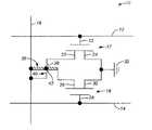
- FIG. 1is a circuit diagram illustrating an embodiment of a memory cell 10 made according to the invention.
- Memory cell 10is typically a component of a semiconductor memory device, such as an RRAM device.
- Memory cell 10includes a program word line 12 , a read word line 14 and a bit line 16 .
- Memory cell 10also includes a program device 17 , in the form of a program transistor, and a read device 18 , in the form of a read transistor.
- Program device 17includes a drain 20 , acting as a first program terminal 20 , a gate 22 , acting as a second program terminal 22 , and a source 24 .
- Read device 18includes a drain 26 , acting as a first read terminal 26 , a gate 28 , acting as a second read terminal, 28 and a source 30 .
- Second program terminal 22is connected to program word line 12 and second read terminal 28 is connected to read word line 14 .
- sources 24 , 30are connected to one another and to ground 32 .
- Memory cell 10also includes a memory element 36 connecting first read terminal 26 with bit line 16 .
- Memory element 36includes a memory region 38 comprising a memory material having an electrical property state can be changed by the application of energy. It is currently believed that the memory material will be a programmable resistive type of memory material, in particular a phase change material. Various types of phase change materials are discussed in more detail below. However, other types of memory materials that are currently available but unknown to the present inventor or that are discovered in the future, may be suitable for use with the present invention.
- Memory cell 10also includes an energy emitting element 40 electrically connecting first program terminal 20 with bit line 16 . Energy emitting element 40 includes an energy emitting region 42 . Energy emitting region 42 is in an energy transmitting relationship with memory region 38 . In the embodiment of FIG.
- energy emitting elementis a resistive element and emits heat type energy so to heat memory region 38 of memory element 36 .
- energy emitting regionis electrically separated from memory region 38 .
- Energy emitting element 40could be constructed to emit other types of energy, such as magnetic field energy or light energy, depending at least in part upon the type of memory material used.
- At least the energy emitting region 42 of energy emitting element 40may be made of an appropriate higher resistance electrical conductor, including for example silicon carbide, carbon, tungsten, and tungsten nitride.
- memory element 36 and energy emitting element 40are oriented generally perpendicular to one another to help minimize the size of memory region 38 . See FIG. 2 .
- the programming of memory cell 10is achieved by passing a current through energy emitting element 40 from program device 17 .
- memory region 38can be heated in a manner to cause memory region to be in a generally crystalline, lower resistance state (that is set) or in a generally amorphous, higher resistance state (that is reset).
- FIGS. 3 and 4illustrates the passing of current through memory element 36 from first read terminal 26 of read device 18 and to bit line 16 for sensing the state of the memory element, typically by a sense amplifier (not shown).
- Memory cell 10electrically isolates memory element 36 from energy emitting element 40 by passing programming currents through energy emitting element 40 but not through memory element 36 and by passing reading current through memory element 36 but not through energy emitting element 40 . Having the separate paths for reading and programming permits the reading current to be increased when compared to conventional programmable resistive memory devices because energy emitting element 40 is not in series with memory element 36 . In addition, the programming current can be decreased when compared to conventional programmable resistive memory devices by using, for example, is a higher resistance energy emitting element 40 . One benefit is a resulting increase in the read speed while another benefit is a reduction in the reset current level.
- phase change materialuseful characteristics include the material having a resistance which is programmable in a reversible manner, such as by having at least two solid phases that can be reversibly induced by electrical current. These at least two phases include an amorphous phase and a crystalline phase. However, in operation, the phase change material may not be fully converted to either an amorphous or crystalline phase. Intermediate phases or mixtures of phases may have a detectable difference in material characteristics. The two solid phases should generally be bistable and have different electrical properties.
- the phase change materialmay be a chalcogenide material.
- a chalcogenide materialmay include GST. In following sections of the disclosure, the phase change is often referred to as GST, and it will be understood that other types of phase change materials can be used.
- a material useful for implementation of a memory cell as described hereinis Ge 2 Sb 2 Te 5 .
- a memory cell 10 as described hereinis readily manufacturable using standard lithography and thin film deposition technologies, without requiring extraordinary steps to form sub-lithographic patterns, while achieving very small dimensions for the region of the cell that actually changes resistivity during programming.
- the memory region 38 in the memory element 36 that changes phaseis preferably small; and accordingly, the magnitude of the reset current required for changing the phase is also small.
- Embodiments of memory cell 10include chalcogenide based materials, and other phase change materials, for memory element 36 .
- Chalcogensinclude any of the four elements oxygen (O), sulfur (S), selenium (Se), and tellurium (Te), forming part of group VI of the periodic table.
- Chalcogenidescomprise compounds of a chalcogen with a more electropositive element or radical.
- Chalcogenide alloyscomprise combinations of chalcogenides with other materials such as transition metals.
- a chalcogenide alloyusually contains one or more elements from column six of the periodic table of elements, such as germanium (Ge) and tin (Sn).
- chalcogenide alloysinclude combinations including one or more of antimony (Sb), gallium (Ga), indium (In), and silver (Ag).
- Sbantimony
- Gagallium
- Inindium
- silversilver
- phase change based memory materialsinclude alloys of: Ga/Sb, In/Sb, In/Se, Sb/Te, Ge/Te, Ge/Sb/Te, In/Sb/Te, Ga/Se/Te, Sn/Sb/Te, In/Sb/Ge, Ag/In/Sb/Te, Ge/Sn/Sb/Te, Ge/Sb/Se/Te and Te/Ge/Sb/S.
- compositionscan be workable.
- the compositionscan be characterized as Te a Ge b Sb 100-(a-b) , where a and b represent atomic percentages that total 100% of the atoms of the constituent elements.
- One researcherhas described the most useful alloys as having an average concentration of Te in the deposited materials well below 70%, typically below about 60% and ranged in general from as low as about 23% up to about 58% Te and most preferably about 48% to 58% Te.
- Concentrations of Gewere above about 5% and ranged from a low of about 8% to about 30% average in the material, remaining generally below 50%. Most preferably, concentrations of Ge ranged from about 8% to about 40%.
- a transition metalsuch as chromium (Cr), iron (Fe), nickel (Ni), niobium (Nb), palladium (Pd), platinum (Pt) and mixtures or alloys thereof may be combined with Ge/Sb/Te to form a phase change alloy that has programmable resistive properties.
- chromium (Cr)iron (Fe), nickel (Ni), niobium (Nb), palladium (Pd), platinum (Pt) and mixtures or alloys thereof
- Ge/Sb/Techromium
- Specific examples of memory materials that may be usefulare given in Ovshinsky '112 at columns 11-3, which examples are hereby incorporated by reference.
- Phase change materialsare capable of being switched between a first structural state in which the material is in a generally amorphous solid phase, and a second structural state in which the material is in a generally crystalline solid phase in its local order in the active channel region of the cell. These phase change materials are at least bistable.
- amorphousis used to refer to a relatively less ordered structure, more disordered than a single crystal, which has the detectable characteristics such as higher electrical resistivity than the crystalline phase.
- crystallineis used to refer to a relatively more ordered structure, more ordered than in an amorphous structure, which has detectable characteristics such as lower electrical resistivity than the amorphous phase.
- phase change materialsmay be electrically switched between different detectable states of local order across the spectrum between completely amorphous and completely crystalline states.
- Other material characteristics affected by the change between amorphous and crystalline phasesinclude atomic order, free electron density and activation energy.
- the materialmay be switched either into different solid phases or into mixtures of two or more solid phases, providing a gray scale between completely amorphous and completely crystalline states.
- the electrical properties in the materialmay vary accordingly.
- Phase change materialscan be changed from one phase state to another by application of electrical pulses. It has been observed that a shorter, higher amplitude pulse tends to change the phase change material to a generally amorphous state, and is referred to as a reset pulse. A longer, lower amplitude pulse tends to change the phase change material to a generally crystalline state, and is referred to as a program pulse. The energy in a shorter, higher amplitude pulse is high enough to allow for bonds of the crystalline structure to be broken and short enough to prevent the atoms from realigning into a crystalline state. Appropriate profiles for pulses can be determined empirically, without undue experimentation, specifically adapted to a particular phase change material and device structure.
- phase change materialThe following is a short summary describing one type of a phase change material.
Landscapes
- Chemical & Material Sciences (AREA)
- Crystallography & Structural Chemistry (AREA)
- Engineering & Computer Science (AREA)
- Computer Hardware Design (AREA)
- Semiconductor Memories (AREA)
Abstract
Description
- International Business Machines Corporation, a New York corporation; Macronix International Corporation, Ltd., a Taiwan corporation, and Infineon Technologies A.G., a German corporation, are parties to a Joint Research Agreement.
- 1. Field of the Invention
- The present invention relates to high density memory devices based on memory materials, for example resistor random access memory (RRAM) devices, and to methods for manufacturing such devices. The memory material is switchable between electrical property states by the application of energy. The memory materials may be phase change based memory materials, including chalcogenide based materials, and other materials.
- 2. Description of Related Art
- Phase change based memory materials are widely used in read-write optical disks. These materials have at least two solid phases, including for example a generally amorphous solid phase and a generally crystalline solid phase. Laser pulses are used in read-write optical disks to switch between phases and to read the optical properties of the material after the phase change.
- Phase change based memory materials, like chalcogenide based materials and similar materials, also can be caused to change phase by application of electrical current through the memory material at levels suitable for implementation in integrated circuits. The generally amorphous state is characterized by higher resistivity than the generally crystalline state; this difference in resistance can be readily sensed to indicate data. These properties have generated interest in using programmable resistive material to form nonvolatile memory circuits, which can be read and written with random access.
- The change from the amorphous to the crystalline state is generally a lower current operation. The change from crystalline to amorphous, referred to as reset herein, is generally a higher current operation, which includes a short high current density pulse to melt or breakdown the crystalline structure, after which the phase change material cools quickly, quenching the phase change process, allowing at least a portion of the phase change structure to stabilize in the amorphous state. It is desirable to minimize the magnitude of the reset current used to cause transition of phase change material from crystalline state to amorphous state. The magnitude of the reset current needed for reset can be reduced by reducing the size of the phase change material element in the cell and by reducing the size of the contact area between electrodes and the phase change material, so that higher current densities are achieved with small absolute current values through the phase change material element.
- One direction of development has been toward using small quantities of programmable resistive material, particularly in small pores. Patents illustrating development toward small pores include: Ovshinsky, “Multibit Single Cell Memory Element Having Tapered Contact,” U.S. Pat. No. 5,687,112, issued Nov. 11, 1997; Zahorik et al., “Method of Making Chalogenide [sic] Memory Device,” U.S. Pat. No. 5,789,277, issued Aug. 4, 1998; Doan et al., “Controllable Ovonic Phase-Change Semiconductor Memory Device and Methods of Fabricating the Same,” U.S. Pat. No. 6,150,253, issued Nov. 21, 2000.
- In phase change memory, data is stored by causing transitions in the phase change material between amorphous and crystalline states using current. Current heats the material and causes transitions between the states. The change from the amorphous to the crystalline state is generally a lower current operation. The change from crystalline to amorphous, referred to as reset herein, is generally a higher current operation. It is desirable to minimize the magnitude of the reset current used to cause transition of phase change material from crystalline state to amorphous state. The magnitude of the reset current needed for reset can be reduced by reducing the size of the active phase change material element in the cell.
- One example of a memory cell, the memory cell being pat of a memory device, comprises a bit line, a read word line and a program word line. The memory cell includes several other elements, including a read device having first and second read terminals, the second read terminal connected to the read word line. A program device has a first and second program terminals, the second program terminal connected to the program word line. A memory element comprises a memory region between first and second memory element terminals. At least the memory region of the memory element comprises a memory material having an electrical property that can be changed by the application of energy. The first memory element terminal is connected to the first read terminal and the second memory element terminal is connected to the bit line. An energy emitting element comprises first and second spaced apart energy emitting element terminals and an energy emitting region between the first and second energy emitting element terminals. The energy emitting region is in an energy-transmitting relationship with the memory region. The first energy emitting element terminal is connected to the first program terminal and the second energy emitting element terminal is connected to the bit line.
- An example of a method for programming a memory cell comprises changing and sensing steps, discussed below. The memory cell is part of a memory device and is of the type comprising several elements. A memory element comprises a memory region between first and second memory element terminals. At least the memory region of the memory element comprises a memory material having an electrical property that can be changed by the application of energy. An energy emitting element comprises first and second spaced apart energy emitting element terminals and an energy emitting region between the first and second energy emitting element terminals. The energy region is in an energy-transmitting relationship with the memory region. The electrical property state of the memory region is changed by passing a first electrical current between the first and second energy emitting element terminals thereby transmitting energy from the energy emitting region to the memory region. The electrical property state of the memory material element is sensed by passing a second electrical current between the first and second memory element terminals. In some methods the electrical property state changing step comprises transmitting heat energy from the energy transmitting region to the memory region.
- Other features, aspects and advantages of the present invention can be seen on review the figures, the detailed description, and the claims which follow.
FIG. 1 is a circuit diagram illustrating a memory cellmate according to the invention;FIG. 2 is an overall view showing the relative orientations of the memory element and the energy emitting element ofFIG. 1 ;FIG. 3 illustrates the structure ofFIG. 2 showing the path of current through the energy emitting element;FIG. 4 is a graph of temperature and voltage versus time illustrating conventional techniques for causing a phase change material to assume a generally crystalline state, typically characterized as “0”, and a generally amorphous state, typically characterized as “1”; andFIG. 5 illustrates the structure ofFIG. 2 showing the path of current through the memory element to permit the state of the memory element to be read.- The following description of the invention will typically be with reference to specific structural embodiments and methods. It is to be understood that there is no intention to limit the invention to the specifically disclosed embodiments and methods but that the invention may be practiced using other features, elements, methods and embodiments. Preferred embodiments are described to illustrate the present invention, not to limit its scope, which is defined by the claims. Those of ordinary skill in the art will recognize a variety of equivalent variations on the description that follows. Like elements in various embodiments are commonly referred to with like reference numerals.
FIG. 1 is a circuit diagram illustrating an embodiment of amemory cell 10 made according to the invention.Memory cell 10 is typically a component of a semiconductor memory device, such as an RRAM device.Memory cell 10 includes aprogram word line 12, aread word line 14 and abit line 16.Memory cell 10 also includes aprogram device 17, in the form of a program transistor, and aread device 18, in the form of a read transistor.Program device 17 includes adrain 20, acting as afirst program terminal 20, agate 22, acting as asecond program terminal 22, and asource 24. Readdevice 18 includes adrain 26, acting as afirst read terminal 26, agate 28, acting as a second read terminal,28 and asource 30.Second program terminal 22 is connected to programword line 12 andsecond read terminal 28 is connected to readword line 14. In this embodiment,sources Memory cell 10 also includes amemory element 36 connectingfirst read terminal 26 withbit line 16.Memory element 36 includes amemory region 38 comprising a memory material having an electrical property state can be changed by the application of energy. It is currently believed that the memory material will be a programmable resistive type of memory material, in particular a phase change material. Various types of phase change materials are discussed in more detail below. However, other types of memory materials that are currently available but unknown to the present inventor or that are discovered in the future, may be suitable for use with the present invention.Memory cell 10 also includes anenergy emitting element 40 electrically connectingfirst program terminal 20 withbit line 16.Energy emitting element 40 includes anenergy emitting region 42.Energy emitting region 42 is in an energy transmitting relationship withmemory region 38. In the embodiment ofFIG. 1 energy emitting element is a resistive element and emits heat type energy so toheat memory region 38 ofmemory element 36. In some embodiments energy emitting region is electrically separated frommemory region 38.Energy emitting element 40 could be constructed to emit other types of energy, such as magnetic field energy or light energy, depending at least in part upon the type of memory material used.- At least the
energy emitting region 42 ofenergy emitting element 40 may be made of an appropriate higher resistance electrical conductor, including for example silicon carbide, carbon, tungsten, and tungsten nitride. - In the disclosed
embodiment memory element 36 andenergy emitting element 40 are oriented generally perpendicular to one another to help minimize the size ofmemory region 38. SeeFIG. 2 . - The programming of
memory cell 10 is achieved by passing a current throughenergy emitting element 40 fromprogram device 17. By the passage of an appropriate current throughenergy emitting element 40,memory region 38 can be heated in a manner to cause memory region to be in a generally crystalline, lower resistance state (that is set) or in a generally amorphous, higher resistance state (that is reset). This passage of current and the heating ofmemory region 38 are suggested inFIGS. 3 and 4 .FIG. 5 illustrates the passing of current throughmemory element 36 fromfirst read terminal 26 ofread device 18 and to bitline 16 for sensing the state of the memory element, typically by a sense amplifier (not shown). Memory cell 10 electrically isolatesmemory element 36 fromenergy emitting element 40 by passing programming currents throughenergy emitting element 40 but not throughmemory element 36 and by passing reading current throughmemory element 36 but not throughenergy emitting element 40. Having the separate paths for reading and programming permits the reading current to be increased when compared to conventional programmable resistive memory devices becauseenergy emitting element 40 is not in series withmemory element 36. In addition, the programming current can be decreased when compared to conventional programmable resistive memory devices by using, for example, is a higher resistanceenergy emitting element 40. One benefit is a resulting increase in the read speed while another benefit is a reduction in the reset current level.- Useful characteristics of a phase change material include the material having a resistance which is programmable in a reversible manner, such as by having at least two solid phases that can be reversibly induced by electrical current. These at least two phases include an amorphous phase and a crystalline phase. However, in operation, the phase change material may not be fully converted to either an amorphous or crystalline phase. Intermediate phases or mixtures of phases may have a detectable difference in material characteristics. The two solid phases should generally be bistable and have different electrical properties. The phase change material may be a chalcogenide material. A chalcogenide material may include GST. In following sections of the disclosure, the phase change is often referred to as GST, and it will be understood that other types of phase change materials can be used. A material useful for implementation of a memory cell as described herein is Ge2Sb2Te5.
- A
memory cell 10 as described herein is readily manufacturable using standard lithography and thin film deposition technologies, without requiring extraordinary steps to form sub-lithographic patterns, while achieving very small dimensions for the region of the cell that actually changes resistivity during programming. Thememory region 38 in thememory element 36 that changes phase is preferably small; and accordingly, the magnitude of the reset current required for changing the phase is also small. - Embodiments of
memory cell 10 include chalcogenide based materials, and other phase change materials, formemory element 36. Chalcogens include any of the four elements oxygen (O), sulfur (S), selenium (Se), and tellurium (Te), forming part of group VI of the periodic table. Chalcogenides comprise compounds of a chalcogen with a more electropositive element or radical. Chalcogenide alloys comprise combinations of chalcogenides with other materials such as transition metals. A chalcogenide alloy usually contains one or more elements from column six of the periodic table of elements, such as germanium (Ge) and tin (Sn). Often, chalcogenide alloys include combinations including one or more of antimony (Sb), gallium (Ga), indium (In), and silver (Ag). Many phase change based memory materials have been described in technical literature, including alloys of: Ga/Sb, In/Sb, In/Se, Sb/Te, Ge/Te, Ge/Sb/Te, In/Sb/Te, Ga/Se/Te, Sn/Sb/Te, In/Sb/Ge, Ag/In/Sb/Te, Ge/Sn/Sb/Te, Ge/Sb/Se/Te and Te/Ge/Sb/S. In the family of Ge/Sb/Te alloys, a wide range of alloy compositions may be workable. The compositions can be characterized as TeaGebSb100-(a-b), where a and b represent atomic percentages that total 100% of the atoms of the constituent elements. One researcher has described the most useful alloys as having an average concentration of Te in the deposited materials well below 70%, typically below about 60% and ranged in general from as low as about 23% up to about 58% Te and most preferably about 48% to 58% Te. Concentrations of Ge were above about 5% and ranged from a low of about 8% to about 30% average in the material, remaining generally below 50%. Most preferably, concentrations of Ge ranged from about 8% to about 40%. The remainder of the principal constituent elements in this composition was Sb. (Ovshinsky '112 patent, cols 10-11.) Particular alloys evaluated by another researcher include Ge2Sb2Te5, GeSb2Te4and GeSb4Te7. (Noboru Yamada, “Potential of Ge—Sb—Te Phase-Change Optical Disks for High-Data-Rate Recording”, SPIE v.3109, pp. 28-37 (1997).) More generally, a transition metal such as chromium (Cr), iron (Fe), nickel (Ni), niobium (Nb), palladium (Pd), platinum (Pt) and mixtures or alloys thereof may be combined with Ge/Sb/Te to form a phase change alloy that has programmable resistive properties. Specific examples of memory materials that may be useful are given in Ovshinsky '112 at columns 11-3, which examples are hereby incorporated by reference. - Phase change materials are capable of being switched between a first structural state in which the material is in a generally amorphous solid phase, and a second structural state in which the material is in a generally crystalline solid phase in its local order in the active channel region of the cell. These phase change materials are at least bistable. The term amorphous is used to refer to a relatively less ordered structure, more disordered than a single crystal, which has the detectable characteristics such as higher electrical resistivity than the crystalline phase. The term crystalline is used to refer to a relatively more ordered structure, more ordered than in an amorphous structure, which has detectable characteristics such as lower electrical resistivity than the amorphous phase. Typically, phase change materials may be electrically switched between different detectable states of local order across the spectrum between completely amorphous and completely crystalline states. Other material characteristics affected by the change between amorphous and crystalline phases include atomic order, free electron density and activation energy. The material may be switched either into different solid phases or into mixtures of two or more solid phases, providing a gray scale between completely amorphous and completely crystalline states. The electrical properties in the material may vary accordingly.
- Phase change materials can be changed from one phase state to another by application of electrical pulses. It has been observed that a shorter, higher amplitude pulse tends to change the phase change material to a generally amorphous state, and is referred to as a reset pulse. A longer, lower amplitude pulse tends to change the phase change material to a generally crystalline state, and is referred to as a program pulse. The energy in a shorter, higher amplitude pulse is high enough to allow for bonds of the crystalline structure to be broken and short enough to prevent the atoms from realigning into a crystalline state. Appropriate profiles for pulses can be determined empirically, without undue experimentation, specifically adapted to a particular phase change material and device structure.
- The following is a short summary describing one type of a phase change material.
- Chalcogenide phase change material.
- GexSbyTez
- x:y:z=2:2:5
- Or other compositions with x: 0˜5; y: 0˜5; z: 0˜10
- GeSbTe with doping, such as N—, Si—, Ti—, or other element doping may also be used.
- Formation method: By PVD sputtering or magnetron-sputtering method with reactive gases of Ar, N2, and/or He, etc chalcogenide @ the pressure of 1 mtorr˜100 mtorr. The deposition is usually done at room temperature. The collimator with aspect ratio of 1˜5 can be used to improve the fill-in performance. To improve the fill-in performance, the DC bias of several ten to several hundred volts is also used. On the other hand, the combination of DC bias and the collimator can be used simultaneously.
- The post deposition annealing treatment with vacuum or N2 ambient is sometimes needed to improve the crystallize state of chalcogenide material. The annealing temperature typically ranges 100 C to 400 C with an anneal time of less than 30 minutes.
- The thickness of chalcogenide material depends on the design of cell structure. In general, a chalcogenide material with thickness of higher than8 nm can have a phase change characterization so that the material exhibits at least two stable resistance states.
- For additional information on the manufacture, component materials, use and operation of phase change random access memory devices, see U.S. patent application Ser. No. 11/155,067, filed 17 Jun. 2005, entitled Thin Film Fuse Phase Change Ram And Manufacturing Method, Attorney Docket No. MXIC 1621-1.
- The above descriptions may have used terms such as above, below, top, bottom, over, under, et cetera. These terms are used to aid understanding of the invention are not used in a limiting sense.
- While the present invention is disclosed by reference to the preferred embodiments and examples detailed above, it is to be understood that these examples are intended in an illustrative rather than in a limiting sense. It is contemplated that modifications and combinations will occur to those skilled in the art, which modifications and combinations will be within the spirit of the invention and the scope of the following claims.
- Any and all patents, patent applications and printed publications referred to above are hereby incorporated by reference.
Claims (14)
Priority Applications (3)
| Application Number | Priority Date | Filing Date | Title |
|---|---|---|---|
| US11/672,125US7483292B2 (en) | 2007-02-07 | 2007-02-07 | Memory cell with separate read and program paths |
| TW096105835ATWI324345B (en) | 2007-02-07 | 2007-02-15 | Memory cell with separate read and program paths |
| CN2007101489195ACN101241756B (en) | 2007-02-07 | 2007-09-12 | Memory cells with different read and program paths |
Applications Claiming Priority (1)
| Application Number | Priority Date | Filing Date | Title |
|---|---|---|---|
| US11/672,125US7483292B2 (en) | 2007-02-07 | 2007-02-07 | Memory cell with separate read and program paths |
Publications (2)
| Publication Number | Publication Date |
|---|---|
| US20080186761A1true US20080186761A1 (en) | 2008-08-07 |
| US7483292B2 US7483292B2 (en) | 2009-01-27 |
Family
ID=39676007
Family Applications (1)
| Application Number | Title | Priority Date | Filing Date |
|---|---|---|---|
| US11/672,125Active2027-07-28US7483292B2 (en) | 2007-02-07 | 2007-02-07 | Memory cell with separate read and program paths |
Country Status (3)
| Country | Link |
|---|---|
| US (1) | US7483292B2 (en) |
| CN (1) | CN101241756B (en) |
| TW (1) | TWI324345B (en) |
Cited By (2)
| Publication number | Priority date | Publication date | Assignee | Title |
|---|---|---|---|---|
| US20110122714A1 (en)* | 2009-11-24 | 2011-05-26 | Industrial Technology Research Institute | Control Method For Memory Cell |
| US8750016B2 (en) | 2011-08-30 | 2014-06-10 | Industrial Technology Research Institute | Resistive memory and program verification method thereof |
Families Citing this family (7)
| Publication number | Priority date | Publication date | Assignee | Title |
|---|---|---|---|---|
| US7639523B2 (en)* | 2006-11-08 | 2009-12-29 | Symetrix Corporation | Stabilized resistive switching memory |
| US7778063B2 (en)* | 2006-11-08 | 2010-08-17 | Symetrix Corporation | Non-volatile resistance switching memories and methods of making same |
| US8817521B2 (en) | 2009-11-24 | 2014-08-26 | Industrial Technology Research Institute | Control method for memory cell |
| US8497705B2 (en) | 2010-11-09 | 2013-07-30 | Macronix International Co., Ltd. | Phase change device for interconnection of programmable logic device |
| US8779592B2 (en)* | 2012-05-01 | 2014-07-15 | Taiwan Semiconductor Manufacturing Company, Ltd. | Via-free interconnect structure with self-aligned metal line interconnections |
| US10615225B2 (en)* | 2018-08-22 | 2020-04-07 | International Business Machines Corporation | Multilayer back end of line (BEOL)-stackable cross-point memory array with complementary pass transistor selectors |
| US12360667B2 (en)* | 2023-06-20 | 2025-07-15 | Taiwan Semiconductor Manufacturing Company, Ltd. | Semiconductor device |
Citations (81)
| Publication number | Priority date | Publication date | Assignee | Title |
|---|---|---|---|---|
| US3271591A (en)* | 1963-09-20 | 1966-09-06 | Energy Conversion Devices Inc | Symmetrical current controlling device |
| US3530441A (en)* | 1969-01-15 | 1970-09-22 | Energy Conversion Devices Inc | Method and apparatus for storing and retrieving information |
| US4599705A (en)* | 1979-12-13 | 1986-07-08 | Energy Conversion Devices, Inc. | Programmable cell for use in programmable electronic arrays |
| US4719594A (en)* | 1984-11-01 | 1988-01-12 | Energy Conversion Devices, Inc. | Grooved optical data storage device including a chalcogenide memory layer |
| US4876220A (en)* | 1986-05-16 | 1989-10-24 | Actel Corporation | Method of making programmable low impedance interconnect diode element |
| US5166096A (en)* | 1991-10-29 | 1992-11-24 | International Business Machines Corporation | Process for fabricating self-aligned contact studs for semiconductor structures |
| US5166758A (en)* | 1991-01-18 | 1992-11-24 | Energy Conversion Devices, Inc. | Electrically erasable phase change memory |
| US5177567A (en)* | 1991-07-19 | 1993-01-05 | Energy Conversion Devices, Inc. | Thin-film structure for chalcogenide electrical switching devices and process therefor |
| US5534712A (en)* | 1991-01-18 | 1996-07-09 | Energy Conversion Devices, Inc. | Electrically erasable memory elements characterized by reduced current and improved thermal stability |
| US5687112A (en)* | 1996-04-19 | 1997-11-11 | Energy Conversion Devices, Inc. | Multibit single cell memory element having tapered contact |
| US5754472A (en)* | 1995-12-27 | 1998-05-19 | Hyundai Electronics Industries Co., Ltd. | Flash memory device having a program path the same as a read pre-condition path |
| US5789277A (en)* | 1996-07-22 | 1998-08-04 | Micron Technology, Inc. | Method of making chalogenide memory device |
| US5789758A (en)* | 1995-06-07 | 1998-08-04 | Micron Technology, Inc. | Chalcogenide memory cell with a plurality of chalcogenide electrodes |
| US5814527A (en)* | 1996-07-22 | 1998-09-29 | Micron Technology, Inc. | Method of making small pores defined by a disposable internal spacer for use in chalcogenide memories |
| US5831276A (en)* | 1995-06-07 | 1998-11-03 | Micron Technology, Inc. | Three-dimensional container diode for use with multi-state material in a non-volatile memory cell |
| US5837564A (en)* | 1995-11-01 | 1998-11-17 | Micron Technology, Inc. | Method for optimal crystallization to obtain high electrical performance from chalcogenides |
| US5869843A (en)* | 1995-06-07 | 1999-02-09 | Micron Technology, Inc. | Memory array having a multi-state element and method for forming such array or cells thereof |
| US5879955A (en)* | 1995-06-07 | 1999-03-09 | Micron Technology, Inc. | Method for fabricating an array of ultra-small pores for chalcogenide memory cells |
| US5952671A (en)* | 1997-05-09 | 1999-09-14 | Micron Technology, Inc. | Small electrode for a chalcogenide switching device and method for fabricating same |
| US5970336A (en)* | 1996-08-22 | 1999-10-19 | Micron Technology, Inc. | Method of making memory cell incorporating a chalcogenide element |
| US5985698A (en)* | 1996-07-22 | 1999-11-16 | Micron Technology, Inc. | Fabrication of three dimensional container diode for use with multi-state material in a non-volatile memory cell |
| US6011725A (en)* | 1997-08-01 | 2000-01-04 | Saifun Semiconductors, Ltd. | Two bit non-volatile electrically erasable and programmable semiconductor memory cell utilizing asymmetrical charge trapping |
| US6025220A (en)* | 1996-06-18 | 2000-02-15 | Micron Technology, Inc. | Method of forming a polysilicon diode and devices incorporating such diode |
| US6031287A (en)* | 1997-06-18 | 2000-02-29 | Micron Technology, Inc. | Contact structure and memory element incorporating the same |
| US6034882A (en)* | 1998-11-16 | 2000-03-07 | Matrix Semiconductor, Inc. | Vertically stacked field programmable nonvolatile memory and method of fabrication |
| US6087674A (en)* | 1996-10-28 | 2000-07-11 | Energy Conversion Devices, Inc. | Memory element with memory material comprising phase-change material and dielectric material |
| US6114713A (en)* | 1997-01-28 | 2000-09-05 | Zahorik; Russell C. | Integrated circuit memory cell having a small active area and method of forming same |
| US6117720A (en)* | 1995-06-07 | 2000-09-12 | Micron Technology, Inc. | Method of making an integrated circuit electrode having a reduced contact area |
| US6147395A (en)* | 1996-10-02 | 2000-11-14 | Micron Technology, Inc. | Method for fabricating a small area of contact between electrodes |
| US6177317B1 (en)* | 1999-04-14 | 2001-01-23 | Macronix International Co., Ltd. | Method of making nonvolatile memory devices having reduced resistance diffusion regions |
| US6271090B1 (en)* | 2000-12-22 | 2001-08-07 | Macronix International Co., Ltd. | Method for manufacturing flash memory device with dual floating gates and two bits per cell |
| US6280684B1 (en)* | 1994-12-13 | 2001-08-28 | Ricoh Company, Ltd. | Sputtering target, method of producing the target, optical recording medium fabricated by using the sputtering target, and method of fabricating the optical recording medium |
| US6314014B1 (en)* | 1999-12-16 | 2001-11-06 | Ovonyx, Inc. | Programmable resistance memory arrays with reference cells |
| US6320786B1 (en)* | 2000-12-22 | 2001-11-20 | Macronix International Co., Ltd. | Method of controlling multi-state NROM |
| US6339544B1 (en)* | 2000-09-29 | 2002-01-15 | Intel Corporation | Method to enhance performance of thermal resistor device |
| US6351406B1 (en)* | 1998-11-16 | 2002-02-26 | Matrix Semiconductor, Inc. | Vertically stacked field programmable nonvolatile memory and method of fabrication |
| US6420215B1 (en)* | 2000-04-28 | 2002-07-16 | Matrix Semiconductor, Inc. | Three-dimensional memory array and method of fabrication |
| US6420216B1 (en)* | 2000-03-14 | 2002-07-16 | International Business Machines Corporation | Fuse processing using dielectric planarization pillars |
| US6429064B1 (en)* | 2000-09-29 | 2002-08-06 | Intel Corporation | Reduced contact area of sidewall conductor |
| US6483736B2 (en)* | 1998-11-16 | 2002-11-19 | Matrix Semiconductor, Inc. | Vertically stacked field programmable nonvolatile memory and method of fabrication |
| US6487114B2 (en)* | 2001-02-28 | 2002-11-26 | Macronix International Co., Ltd. | Method of reading two-bit memories of NROM cell |
| US6511867B2 (en)* | 2001-06-30 | 2003-01-28 | Ovonyx, Inc. | Utilizing atomic layer deposition for programmable device |
| US6512241B1 (en)* | 2001-12-31 | 2003-01-28 | Intel Corporation | Phase change material memory device |
| US6514788B2 (en)* | 2001-05-29 | 2003-02-04 | Bae Systems Information And Electronic Systems Integration Inc. | Method for manufacturing contacts for a Chalcogenide memory device |
| US6534781B2 (en)* | 2000-12-26 | 2003-03-18 | Ovonyx, Inc. | Phase-change memory bipolar array utilizing a single shallow trench isolation for creating an individual active area region for two memory array elements and one bipolar base contact |
| US6545903B1 (en)* | 2001-12-17 | 2003-04-08 | Texas Instruments Incorporated | Self-aligned resistive plugs for forming memory cell with phase change material |
| US6555860B2 (en)* | 2000-09-29 | 2003-04-29 | Intel Corporation | Compositionally modified resistive electrode |
| US6563156B2 (en)* | 2001-03-15 | 2003-05-13 | Micron Technology, Inc. | Memory elements and methods for making same |
| US6566700B2 (en)* | 2001-10-11 | 2003-05-20 | Ovonyx, Inc. | Carbon-containing interfacial layer for phase-change memory |
| US6567293B1 (en)* | 2000-09-29 | 2003-05-20 | Ovonyx, Inc. | Single level metal memory cell using chalcogenide cladding |
| US6579760B1 (en)* | 2002-03-28 | 2003-06-17 | Macronix International Co., Ltd. | Self-aligned, programmable phase change memory |
| US6586761B2 (en)* | 2001-09-07 | 2003-07-01 | Intel Corporation | Phase change material memory device |
| US6589714B2 (en)* | 2001-06-26 | 2003-07-08 | Ovonyx, Inc. | Method for making programmable resistance memory element using silylated photoresist |
| US6605527B2 (en)* | 2001-06-30 | 2003-08-12 | Intel Corporation | Reduced area intersection between electrode and programming element |
| US6605821B1 (en)* | 2002-05-10 | 2003-08-12 | Hewlett-Packard Development Company, L.P. | Phase change material electronic memory structure and method for forming |
| US6607974B2 (en)* | 2000-07-14 | 2003-08-19 | Micron Technology, Inc. | Method of forming a contact structure in a semiconductor device |
| US6613604B2 (en)* | 2001-08-02 | 2003-09-02 | Ovonyx, Inc. | Method for making small pore for use in programmable resistance memory element |
| US6617192B1 (en)* | 1997-10-01 | 2003-09-09 | Ovonyx, Inc. | Electrically programmable memory element with multi-regioned contact |
| US6627530B2 (en)* | 2000-12-22 | 2003-09-30 | Matrix Semiconductor, Inc. | Patterning three dimensional structures |
| US6639849B2 (en)* | 2002-02-28 | 2003-10-28 | Fujitsu Limited | Nonvolatile semiconductor memory device programming second dynamic reference cell according to threshold value of first dynamic reference cell |
| US6673700B2 (en)* | 2001-06-30 | 2004-01-06 | Ovonyx, Inc. | Reduced area intersection between electrode and programming element |
| US6744088B1 (en)* | 2002-12-13 | 2004-06-01 | Intel Corporation | Phase change memory device on a planar composite layer |
| US6791102B2 (en)* | 2002-12-13 | 2004-09-14 | Intel Corporation | Phase change memory |
| US6797979B2 (en)* | 2000-12-21 | 2004-09-28 | Intel Corporation | Metal structure for a phase-change memory device |
| US6805563B2 (en)* | 2002-09-10 | 2004-10-19 | Enplas Corporation | Socket for electrical parts |
| US6815704B1 (en)* | 2003-09-04 | 2004-11-09 | Silicon Storage Technology, Inc. | Phase change memory device employing thermally insulating voids |
| US6859389B2 (en)* | 2002-10-31 | 2005-02-22 | Dai Nippon Printing Co., Ltd. | Phase change-type memory element and process for producing the same |
| US6861267B2 (en)* | 2001-09-17 | 2005-03-01 | Intel Corporation | Reducing shunts in memories with phase-change material |
| US6864500B2 (en)* | 2002-04-10 | 2005-03-08 | Micron Technology, Inc. | Programmable conductor memory cell structure |
| US6864503B2 (en)* | 2002-08-09 | 2005-03-08 | Macronix International Co., Ltd. | Spacer chalcogenide memory method and device |
| US6867638B2 (en)* | 2002-01-10 | 2005-03-15 | Silicon Storage Technology, Inc. | High voltage generation and regulation system for digital multilevel nonvolatile memory |
| US6888750B2 (en)* | 2000-04-28 | 2005-05-03 | Matrix Semiconductor, Inc. | Nonvolatile memory on SOI and compound semiconductor substrates and method of fabrication |
| US6894305B2 (en)* | 2003-02-24 | 2005-05-17 | Samsung Electronics Co., Ltd. | Phase-change memory devices with a self-heater structure |
| US6909107B2 (en)* | 2002-12-30 | 2005-06-21 | Bae Systems, Information And Electronic Systems Integration, Inc. | Method for manufacturing sidewall contacts for a chalcogenide memory device |
| US6927410B2 (en)* | 2003-09-04 | 2005-08-09 | Silicon Storage Technology, Inc. | Memory device with discrete layers of phase change memory material |
| US6933516B2 (en)* | 2001-10-11 | 2005-08-23 | Ovonyx, Inc. | Forming tapered lower electrode phase-change memories |
| US6936840B2 (en)* | 2004-01-30 | 2005-08-30 | International Business Machines Corporation | Phase-change memory cell and method of fabricating the phase-change memory cell |
| US6937507B2 (en)* | 2003-12-05 | 2005-08-30 | Silicon Storage Technology, Inc. | Memory device and method of operating same |
| US20050215009A1 (en)* | 2004-03-19 | 2005-09-29 | Sung-Lae Cho | Methods of forming phase-change memory devices |
| US6992932B2 (en)* | 2002-10-29 | 2006-01-31 | Saifun Semiconductors Ltd | Method circuit and system for read error detection in a non-volatile memory array |
| US7042001B2 (en)* | 2004-01-29 | 2006-05-09 | Samsung Electronics Co., Ltd. | Phase change memory devices including memory elements having variable cross-sectional areas |
Family Cites Families (68)
| Publication number | Priority date | Publication date | Assignee | Title |
|---|---|---|---|---|
| JP2685770B2 (en) | 1987-12-28 | 1997-12-03 | 株式会社東芝 | Nonvolatile semiconductor memory device |
| JP2825031B2 (en) | 1991-08-06 | 1998-11-18 | 日本電気株式会社 | Semiconductor memory device |
| US5958358A (en) | 1992-07-08 | 1999-09-28 | Yeda Research And Development Co., Ltd. | Oriented polycrystalline thin films of transition metal chalcogenides |
| JP2884962B2 (en) | 1992-10-30 | 1999-04-19 | 日本電気株式会社 | Semiconductor memory |
| US5515488A (en) | 1994-08-30 | 1996-05-07 | Xerox Corporation | Method and apparatus for concurrent graphical visualization of a database search and its search history |
| US5866928A (en) | 1996-07-16 | 1999-02-02 | Micron Technology, Inc. | Single digit line with cell contact interconnect |
| US5902704A (en) | 1997-07-02 | 1999-05-11 | Lsi Logic Corporation | Process for forming photoresist mask over integrated circuit structures with critical dimension control |
| US7023009B2 (en) | 1997-10-01 | 2006-04-04 | Ovonyx, Inc. | Electrically programmable memory element with improved contacts |
| US6372651B1 (en) | 1998-07-17 | 2002-04-16 | Advanced Micro Devices, Inc. | Method for trimming a photoresist pattern line for memory gate etching |
| DE19903325B4 (en) | 1999-01-28 | 2004-07-22 | Heckler & Koch Gmbh | Locked breech for a self-loading handgun, with a breech head and breech carrier and a resilient locking ring with a longitudinal slot |
| US6075719A (en) | 1999-06-22 | 2000-06-13 | Energy Conversion Devices, Inc. | Method of programming phase-change memory element |
| US6077674A (en) | 1999-10-27 | 2000-06-20 | Agilent Technologies Inc. | Method of producing oligonucleotide arrays with features of high purity |
| US6501111B1 (en) | 2000-06-30 | 2002-12-31 | Intel Corporation | Three-dimensional (3D) programmable device |
| JP4056392B2 (en) | 2001-01-30 | 2008-03-05 | 株式会社ルネサステクノロジ | Semiconductor integrated circuit device |
| US6730928B2 (en) | 2001-05-09 | 2004-05-04 | Science Applications International Corporation | Phase change switches and circuits coupling to electromagnetic waves containing phase change switches |
| US6643165B2 (en) | 2001-07-25 | 2003-11-04 | Nantero, Inc. | Electromechanical memory having cell selection circuitry constructed with nanotube technology |
| US6709958B2 (en) | 2001-08-30 | 2004-03-23 | Micron Technology, Inc. | Integrated circuit device and fabrication using metal-doped chalcogenide materials |
| US6972430B2 (en) | 2002-02-20 | 2005-12-06 | Stmicroelectronics S.R.L. | Sublithographic contact structure, phase change memory cell with optimized heater shape, and manufacturing method thereof |
| US7122281B2 (en) | 2002-02-26 | 2006-10-17 | Synopsys, Inc. | Critical dimension control using full phase and trim masks |
| US6620715B1 (en) | 2002-03-29 | 2003-09-16 | Cypress Semiconductor Corp. | Method for forming sub-critical dimension structures in an integrated circuit |
| US6850432B2 (en) | 2002-08-20 | 2005-02-01 | Macronix International Co., Ltd. | Laser programmable electrically readable phase-change memory method and device |
| JP4190238B2 (en) | 2002-09-13 | 2008-12-03 | 株式会社ルネサステクノロジ | Nonvolatile semiconductor memory device |
| US7277317B2 (en) | 2003-01-31 | 2007-10-02 | Nxp B.V. | MRAM architecture for low power consumption and high selectivity |
| US7067865B2 (en) | 2003-06-06 | 2006-06-27 | Macronix International Co., Ltd. | High density chalcogenide memory cells |
| US7893419B2 (en) | 2003-08-04 | 2011-02-22 | Intel Corporation | Processing phase change material to improve programming speed |
| US6808991B1 (en) | 2003-11-19 | 2004-10-26 | Macronix International Co., Ltd. | Method for forming twin bit cell flash memory |
| JP4124743B2 (en) | 2004-01-21 | 2008-07-23 | 株式会社ルネサステクノロジ | Phase change memory |
| JP4529493B2 (en) | 2004-03-12 | 2010-08-25 | 株式会社日立製作所 | Semiconductor device |
| DE102004014487A1 (en) | 2004-03-24 | 2005-11-17 | Infineon Technologies Ag | Memory device with embedded in insulating material, active material |
| US7365385B2 (en) | 2004-08-30 | 2008-04-29 | Micron Technology, Inc. | DRAM layout with vertical FETs and method of formation |
| US7608503B2 (en) | 2004-11-22 | 2009-10-27 | Macronix International Co., Ltd. | Side wall active pin memory and manufacturing method |
| US7220983B2 (en) | 2004-12-09 | 2007-05-22 | Macronix International Co., Ltd. | Self-aligned small contact phase-change memory method and device |
| US7419771B2 (en) | 2005-01-11 | 2008-09-02 | Taiwan Semiconductor Manufacturing Co., Ltd. | Method for forming a finely patterned resist |
| US7214958B2 (en) | 2005-02-10 | 2007-05-08 | Infineon Technologies Ag | Phase change memory cell with high read margin at low power operation |
| US7166533B2 (en) | 2005-04-08 | 2007-01-23 | Infineon Technologies, Ag | Phase change memory cell defined by a pattern shrink material process |
| US7238994B2 (en) | 2005-06-17 | 2007-07-03 | Macronix International Co., Ltd. | Thin film plate phase change ram circuit and manufacturing method |
| US7514367B2 (en) | 2005-06-17 | 2009-04-07 | Macronix International Co., Ltd. | Method for manufacturing a narrow structure on an integrated circuit |
| US7534647B2 (en) | 2005-06-17 | 2009-05-19 | Macronix International Co., Ltd. | Damascene phase change RAM and manufacturing method |
| US8237140B2 (en) | 2005-06-17 | 2012-08-07 | Macronix International Co., Ltd. | Self-aligned, embedded phase change RAM |
| US7514288B2 (en) | 2005-06-17 | 2009-04-07 | Macronix International Co., Ltd. | Manufacturing methods for thin film fuse phase change ram |
| US7598512B2 (en) | 2005-06-17 | 2009-10-06 | Macronix International Co., Ltd. | Thin film fuse phase change cell with thermal isolation layer and manufacturing method |
| US7321130B2 (en) | 2005-06-17 | 2008-01-22 | Macronix International Co., Ltd. | Thin film fuse phase change RAM and manufacturing method |
| US20070111429A1 (en) | 2005-11-14 | 2007-05-17 | Macronix International Co., Ltd. | Method of manufacturing a pipe shaped phase change memory |
| US7397060B2 (en) | 2005-11-14 | 2008-07-08 | Macronix International Co., Ltd. | Pipe shaped phase change memory |
| US7635855B2 (en) | 2005-11-15 | 2009-12-22 | Macronix International Co., Ltd. | I-shaped phase change memory cell |
| US7450411B2 (en) | 2005-11-15 | 2008-11-11 | Macronix International Co., Ltd. | Phase change memory device and manufacturing method |
| US7786460B2 (en) | 2005-11-15 | 2010-08-31 | Macronix International Co., Ltd. | Phase change memory device and manufacturing method |
| US7394088B2 (en) | 2005-11-15 | 2008-07-01 | Macronix International Co., Ltd. | Thermally contained/insulated phase change memory device and method (combined) |
| US7414258B2 (en) | 2005-11-16 | 2008-08-19 | Macronix International Co., Ltd. | Spacer electrode small pin phase change memory RAM and manufacturing method |
| US7829876B2 (en) | 2005-11-21 | 2010-11-09 | Macronix International Co., Ltd. | Vacuum cell thermal isolation for a phase change memory device |
| US7479649B2 (en) | 2005-11-21 | 2009-01-20 | Macronix International Co., Ltd. | Vacuum jacketed electrode for phase change memory element |
| US7507986B2 (en) | 2005-11-21 | 2009-03-24 | Macronix International Co., Ltd. | Thermal isolation for an active-sidewall phase change memory cell |
| US7449710B2 (en) | 2005-11-21 | 2008-11-11 | Macronix International Co., Ltd. | Vacuum jacket for phase change memory element |
| US7599217B2 (en) | 2005-11-22 | 2009-10-06 | Macronix International Co., Ltd. | Memory cell device and manufacturing method |
| US7459717B2 (en) | 2005-11-28 | 2008-12-02 | Macronix International Co., Ltd. | Phase change memory cell and manufacturing method |
| US7688619B2 (en) | 2005-11-28 | 2010-03-30 | Macronix International Co., Ltd. | Phase change memory cell and manufacturing method |
| US7605079B2 (en) | 2005-12-05 | 2009-10-20 | Macronix International Co., Ltd. | Manufacturing method for phase change RAM with electrode layer process |
| US7642539B2 (en) | 2005-12-13 | 2010-01-05 | Macronix International Co., Ltd. | Thin film fuse phase change cell with thermal isolation pad and manufacturing method |
| US7531825B2 (en) | 2005-12-27 | 2009-05-12 | Macronix International Co., Ltd. | Method for forming self-aligned thermal isolation cell for a variable resistance memory array |
| US8062833B2 (en) | 2005-12-30 | 2011-11-22 | Macronix International Co., Ltd. | Chalcogenide layer etching method |
| US7560337B2 (en) | 2006-01-09 | 2009-07-14 | Macronix International Co., Ltd. | Programmable resistive RAM and manufacturing method |
| US7595218B2 (en) | 2006-01-09 | 2009-09-29 | Macronix International Co., Ltd. | Programmable resistive RAM and manufacturing method |
| US20070158632A1 (en) | 2006-01-09 | 2007-07-12 | Macronix International Co., Ltd. | Method for Fabricating a Pillar-Shaped Phase Change Memory Element |
| US7741636B2 (en) | 2006-01-09 | 2010-06-22 | Macronix International Co., Ltd. | Programmable resistive RAM and manufacturing method |
| US7825396B2 (en) | 2006-01-11 | 2010-11-02 | Macronix International Co., Ltd. | Self-align planerized bottom electrode phase change memory and manufacturing method |
| US7432206B2 (en) | 2006-01-24 | 2008-10-07 | Macronix International Co., Ltd. | Self-aligned manufacturing method, and manufacturing method for thin film fuse phase change ram |
| US7456421B2 (en) | 2006-01-30 | 2008-11-25 | Macronix International Co., Ltd. | Vertical side wall active pin structures in a phase change memory and manufacturing methods |
| US7928421B2 (en) | 2006-04-21 | 2011-04-19 | Macronix International Co., Ltd. | Phase change memory cell with vacuum spacer |
- 2007
- 2007-02-07USUS11/672,125patent/US7483292B2/enactiveActive
- 2007-02-15TWTW096105835Apatent/TWI324345B/enactive
- 2007-09-12CNCN2007101489195Apatent/CN101241756B/enactiveActive
Patent Citations (99)
| Publication number | Priority date | Publication date | Assignee | Title |
|---|---|---|---|---|
| US3271591A (en)* | 1963-09-20 | 1966-09-06 | Energy Conversion Devices Inc | Symmetrical current controlling device |
| US3530441A (en)* | 1969-01-15 | 1970-09-22 | Energy Conversion Devices Inc | Method and apparatus for storing and retrieving information |
| US4599705A (en)* | 1979-12-13 | 1986-07-08 | Energy Conversion Devices, Inc. | Programmable cell for use in programmable electronic arrays |
| US4719594A (en)* | 1984-11-01 | 1988-01-12 | Energy Conversion Devices, Inc. | Grooved optical data storage device including a chalcogenide memory layer |
| US4876220A (en)* | 1986-05-16 | 1989-10-24 | Actel Corporation | Method of making programmable low impedance interconnect diode element |
| US5166758A (en)* | 1991-01-18 | 1992-11-24 | Energy Conversion Devices, Inc. | Electrically erasable phase change memory |
| US5534712A (en)* | 1991-01-18 | 1996-07-09 | Energy Conversion Devices, Inc. | Electrically erasable memory elements characterized by reduced current and improved thermal stability |
| US5177567A (en)* | 1991-07-19 | 1993-01-05 | Energy Conversion Devices, Inc. | Thin-film structure for chalcogenide electrical switching devices and process therefor |
| US5166096A (en)* | 1991-10-29 | 1992-11-24 | International Business Machines Corporation | Process for fabricating self-aligned contact studs for semiconductor structures |
| US6280684B1 (en)* | 1994-12-13 | 2001-08-28 | Ricoh Company, Ltd. | Sputtering target, method of producing the target, optical recording medium fabricated by using the sputtering target, and method of fabricating the optical recording medium |
| US5831276A (en)* | 1995-06-07 | 1998-11-03 | Micron Technology, Inc. | Three-dimensional container diode for use with multi-state material in a non-volatile memory cell |
| US6420725B1 (en)* | 1995-06-07 | 2002-07-16 | Micron Technology, Inc. | Method and apparatus for forming an integrated circuit electrode having a reduced contact area |
| US5789758A (en)* | 1995-06-07 | 1998-08-04 | Micron Technology, Inc. | Chalcogenide memory cell with a plurality of chalcogenide electrodes |
| US6077729A (en)* | 1995-06-07 | 2000-06-20 | Micron Technology, Inc. | Memory array having a multi-state element and method for forming such array or cellis thereof |
| US6104038A (en)* | 1995-06-07 | 2000-08-15 | Micron Technology, Inc. | Method for fabricating an array of ultra-small pores for chalcogenide memory cells |
| US5869843A (en)* | 1995-06-07 | 1999-02-09 | Micron Technology, Inc. | Memory array having a multi-state element and method for forming such array or cells thereof |
| US5879955A (en)* | 1995-06-07 | 1999-03-09 | Micron Technology, Inc. | Method for fabricating an array of ultra-small pores for chalcogenide memory cells |
| US5920788A (en)* | 1995-06-07 | 1999-07-06 | Micron Technology, Inc. | Chalcogenide memory cell with a plurality of chalcogenide electrodes |
| US6117720A (en)* | 1995-06-07 | 2000-09-12 | Micron Technology, Inc. | Method of making an integrated circuit electrode having a reduced contact area |
| US5837564A (en)* | 1995-11-01 | 1998-11-17 | Micron Technology, Inc. | Method for optimal crystallization to obtain high electrical performance from chalcogenides |
| US5754472A (en)* | 1995-12-27 | 1998-05-19 | Hyundai Electronics Industries Co., Ltd. | Flash memory device having a program path the same as a read pre-condition path |
| USRE37259E1 (en)* | 1996-04-19 | 2001-07-03 | Energy Conversion Devices, Inc. | Multibit single cell memory element having tapered contact |
| US5687112A (en)* | 1996-04-19 | 1997-11-11 | Energy Conversion Devices, Inc. | Multibit single cell memory element having tapered contact |
| US6025220A (en)* | 1996-06-18 | 2000-02-15 | Micron Technology, Inc. | Method of forming a polysilicon diode and devices incorporating such diode |
| US5985698A (en)* | 1996-07-22 | 1999-11-16 | Micron Technology, Inc. | Fabrication of three dimensional container diode for use with multi-state material in a non-volatile memory cell |
| US5789277A (en)* | 1996-07-22 | 1998-08-04 | Micron Technology, Inc. | Method of making chalogenide memory device |
| US5814527A (en)* | 1996-07-22 | 1998-09-29 | Micron Technology, Inc. | Method of making small pores defined by a disposable internal spacer for use in chalcogenide memories |
| US6111264A (en)* | 1996-07-22 | 2000-08-29 | Micron Technology, Inc. | Small pores defined by a disposable internal spacer for use in chalcogenide memories |
| US5970336A (en)* | 1996-08-22 | 1999-10-19 | Micron Technology, Inc. | Method of making memory cell incorporating a chalcogenide element |
| US6153890A (en)* | 1996-08-22 | 2000-11-28 | Micron Technology, Inc. | Memory cell incorporating a chalcogenide element |
| US6236059B1 (en)* | 1996-08-22 | 2001-05-22 | Micron Technology, Inc. | Memory cell incorporating a chalcogenide element and method of making same |
| US6423621B2 (en)* | 1996-10-02 | 2002-07-23 | Micron Technology, Inc. | Controllable ovonic phase-change semiconductor memory device and methods of fabricating the same |
| US6147395A (en)* | 1996-10-02 | 2000-11-14 | Micron Technology, Inc. | Method for fabricating a small area of contact between electrodes |
| US6150253A (en)* | 1996-10-02 | 2000-11-21 | Micron Technology, Inc. | Controllable ovonic phase-change semiconductor memory device and methods of fabricating the same |
| US6462353B1 (en)* | 1996-10-02 | 2002-10-08 | Micron Technology Inc. | Method for fabricating a small area of contact between electrodes |
| US6287887B1 (en)* | 1996-10-02 | 2001-09-11 | Micron Technology, Inc. | Method for fabricating a small area of contact between electrodes |
| US6087674A (en)* | 1996-10-28 | 2000-07-11 | Energy Conversion Devices, Inc. | Memory element with memory material comprising phase-change material and dielectric material |
| US6114713A (en)* | 1997-01-28 | 2000-09-05 | Zahorik; Russell C. | Integrated circuit memory cell having a small active area and method of forming same |
| US6189582B1 (en)* | 1997-05-09 | 2001-02-20 | Micron Technology, Inc. | Small electrode for a chalcogenide switching device and method for fabricating same |
| US5952671A (en)* | 1997-05-09 | 1999-09-14 | Micron Technology, Inc. | Small electrode for a chalcogenide switching device and method for fabricating same |
| US6031287A (en)* | 1997-06-18 | 2000-02-29 | Micron Technology, Inc. | Contact structure and memory element incorporating the same |
| US6011725A (en)* | 1997-08-01 | 2000-01-04 | Saifun Semiconductors, Ltd. | Two bit non-volatile electrically erasable and programmable semiconductor memory cell utilizing asymmetrical charge trapping |
| US6617192B1 (en)* | 1997-10-01 | 2003-09-09 | Ovonyx, Inc. | Electrically programmable memory element with multi-regioned contact |
| US6185122B1 (en)* | 1998-11-16 | 2001-02-06 | Matrix Semiconductor, Inc. | Vertically stacked field programmable nonvolatile memory and method of fabrication |
| US6483736B2 (en)* | 1998-11-16 | 2002-11-19 | Matrix Semiconductor, Inc. | Vertically stacked field programmable nonvolatile memory and method of fabrication |
| US6351406B1 (en)* | 1998-11-16 | 2002-02-26 | Matrix Semiconductor, Inc. | Vertically stacked field programmable nonvolatile memory and method of fabrication |
| US6034882A (en)* | 1998-11-16 | 2000-03-07 | Matrix Semiconductor, Inc. | Vertically stacked field programmable nonvolatile memory and method of fabrication |
| US6177317B1 (en)* | 1999-04-14 | 2001-01-23 | Macronix International Co., Ltd. | Method of making nonvolatile memory devices having reduced resistance diffusion regions |
| US6314014B1 (en)* | 1999-12-16 | 2001-11-06 | Ovonyx, Inc. | Programmable resistance memory arrays with reference cells |
| US6420216B1 (en)* | 2000-03-14 | 2002-07-16 | International Business Machines Corporation | Fuse processing using dielectric planarization pillars |
| US6420215B1 (en)* | 2000-04-28 | 2002-07-16 | Matrix Semiconductor, Inc. | Three-dimensional memory array and method of fabrication |
| US6888750B2 (en)* | 2000-04-28 | 2005-05-03 | Matrix Semiconductor, Inc. | Nonvolatile memory on SOI and compound semiconductor substrates and method of fabrication |
| US6607974B2 (en)* | 2000-07-14 | 2003-08-19 | Micron Technology, Inc. | Method of forming a contact structure in a semiconductor device |
| US6621095B2 (en)* | 2000-09-29 | 2003-09-16 | Ovonyx, Inc. | Method to enhance performance of thermal resistor device |
| US6339544B1 (en)* | 2000-09-29 | 2002-01-15 | Intel Corporation | Method to enhance performance of thermal resistor device |
| US6597009B2 (en)* | 2000-09-29 | 2003-07-22 | Intel Corporation | Reduced contact area of sidewall conductor |
| US6567293B1 (en)* | 2000-09-29 | 2003-05-20 | Ovonyx, Inc. | Single level metal memory cell using chalcogenide cladding |
| US6429064B1 (en)* | 2000-09-29 | 2002-08-06 | Intel Corporation | Reduced contact area of sidewall conductor |
| US6555860B2 (en)* | 2000-09-29 | 2003-04-29 | Intel Corporation | Compositionally modified resistive electrode |
| US6797979B2 (en)* | 2000-12-21 | 2004-09-28 | Intel Corporation | Metal structure for a phase-change memory device |
| US6271090B1 (en)* | 2000-12-22 | 2001-08-07 | Macronix International Co., Ltd. | Method for manufacturing flash memory device with dual floating gates and two bits per cell |
| US6627530B2 (en)* | 2000-12-22 | 2003-09-30 | Matrix Semiconductor, Inc. | Patterning three dimensional structures |
| US6320786B1 (en)* | 2000-12-22 | 2001-11-20 | Macronix International Co., Ltd. | Method of controlling multi-state NROM |
| US6534781B2 (en)* | 2000-12-26 | 2003-03-18 | Ovonyx, Inc. | Phase-change memory bipolar array utilizing a single shallow trench isolation for creating an individual active area region for two memory array elements and one bipolar base contact |
| US6593176B2 (en)* | 2000-12-26 | 2003-07-15 | Ovonyx, Inc. | Method for forming phase-change memory bipolar array utilizing a single shallow trench isolation for creating an individual active area region for two memory array elements and one bipolar base contact |
| US6487114B2 (en)* | 2001-02-28 | 2002-11-26 | Macronix International Co., Ltd. | Method of reading two-bit memories of NROM cell |
| US6563156B2 (en)* | 2001-03-15 | 2003-05-13 | Micron Technology, Inc. | Memory elements and methods for making same |
| US6514788B2 (en)* | 2001-05-29 | 2003-02-04 | Bae Systems Information And Electronic Systems Integration Inc. | Method for manufacturing contacts for a Chalcogenide memory device |
| US6589714B2 (en)* | 2001-06-26 | 2003-07-08 | Ovonyx, Inc. | Method for making programmable resistance memory element using silylated photoresist |
| US6605527B2 (en)* | 2001-06-30 | 2003-08-12 | Intel Corporation | Reduced area intersection between electrode and programming element |
| US6673700B2 (en)* | 2001-06-30 | 2004-01-06 | Ovonyx, Inc. | Reduced area intersection between electrode and programming element |
| US6511867B2 (en)* | 2001-06-30 | 2003-01-28 | Ovonyx, Inc. | Utilizing atomic layer deposition for programmable device |
| US6613604B2 (en)* | 2001-08-02 | 2003-09-02 | Ovonyx, Inc. | Method for making small pore for use in programmable resistance memory element |
| US6586761B2 (en)* | 2001-09-07 | 2003-07-01 | Intel Corporation | Phase change material memory device |
| US6861267B2 (en)* | 2001-09-17 | 2005-03-01 | Intel Corporation | Reducing shunts in memories with phase-change material |
| US6566700B2 (en)* | 2001-10-11 | 2003-05-20 | Ovonyx, Inc. | Carbon-containing interfacial layer for phase-change memory |
| US6933516B2 (en)* | 2001-10-11 | 2005-08-23 | Ovonyx, Inc. | Forming tapered lower electrode phase-change memories |
| US6545903B1 (en)* | 2001-12-17 | 2003-04-08 | Texas Instruments Incorporated | Self-aligned resistive plugs for forming memory cell with phase change material |
| US6512241B1 (en)* | 2001-12-31 | 2003-01-28 | Intel Corporation | Phase change material memory device |
| US6867638B2 (en)* | 2002-01-10 | 2005-03-15 | Silicon Storage Technology, Inc. | High voltage generation and regulation system for digital multilevel nonvolatile memory |
| US6639849B2 (en)* | 2002-02-28 | 2003-10-28 | Fujitsu Limited | Nonvolatile semiconductor memory device programming second dynamic reference cell according to threshold value of first dynamic reference cell |
| US6579760B1 (en)* | 2002-03-28 | 2003-06-17 | Macronix International Co., Ltd. | Self-aligned, programmable phase change memory |
| US6864500B2 (en)* | 2002-04-10 | 2005-03-08 | Micron Technology, Inc. | Programmable conductor memory cell structure |
| US6605821B1 (en)* | 2002-05-10 | 2003-08-12 | Hewlett-Packard Development Company, L.P. | Phase change material electronic memory structure and method for forming |
| US6864503B2 (en)* | 2002-08-09 | 2005-03-08 | Macronix International Co., Ltd. | Spacer chalcogenide memory method and device |
| US20050093022A1 (en)* | 2002-08-09 | 2005-05-05 | Macronix International Co., Ltd. | Spacer chalcogenide memory device |
| US6805563B2 (en)* | 2002-09-10 | 2004-10-19 | Enplas Corporation | Socket for electrical parts |
| US6992932B2 (en)* | 2002-10-29 | 2006-01-31 | Saifun Semiconductors Ltd | Method circuit and system for read error detection in a non-volatile memory array |
| US6859389B2 (en)* | 2002-10-31 | 2005-02-22 | Dai Nippon Printing Co., Ltd. | Phase change-type memory element and process for producing the same |
| US6791102B2 (en)* | 2002-12-13 | 2004-09-14 | Intel Corporation | Phase change memory |
| US6744088B1 (en)* | 2002-12-13 | 2004-06-01 | Intel Corporation | Phase change memory device on a planar composite layer |
| US6909107B2 (en)* | 2002-12-30 | 2005-06-21 | Bae Systems, Information And Electronic Systems Integration, Inc. | Method for manufacturing sidewall contacts for a chalcogenide memory device |
| US6894305B2 (en)* | 2003-02-24 | 2005-05-17 | Samsung Electronics Co., Ltd. | Phase-change memory devices with a self-heater structure |
| US6815704B1 (en)* | 2003-09-04 | 2004-11-09 | Silicon Storage Technology, Inc. | Phase change memory device employing thermally insulating voids |
| US6927410B2 (en)* | 2003-09-04 | 2005-08-09 | Silicon Storage Technology, Inc. | Memory device with discrete layers of phase change memory material |
| US6937507B2 (en)* | 2003-12-05 | 2005-08-30 | Silicon Storage Technology, Inc. | Memory device and method of operating same |
| US7042001B2 (en)* | 2004-01-29 | 2006-05-09 | Samsung Electronics Co., Ltd. | Phase change memory devices including memory elements having variable cross-sectional areas |
| US6936840B2 (en)* | 2004-01-30 | 2005-08-30 | International Business Machines Corporation | Phase-change memory cell and method of fabricating the phase-change memory cell |
| US20050215009A1 (en)* | 2004-03-19 | 2005-09-29 | Sung-Lae Cho | Methods of forming phase-change memory devices |
Cited By (3)
| Publication number | Priority date | Publication date | Assignee | Title |
|---|---|---|---|---|
| US20110122714A1 (en)* | 2009-11-24 | 2011-05-26 | Industrial Technology Research Institute | Control Method For Memory Cell |
| US8223528B2 (en) | 2009-11-24 | 2012-07-17 | Industrial Technology Research Institute | Control method for memory cell |
| US8750016B2 (en) | 2011-08-30 | 2014-06-10 | Industrial Technology Research Institute | Resistive memory and program verification method thereof |
Also Published As
| Publication number | Publication date |
|---|---|
| CN101241756B (en) | 2011-06-15 |
| US7483292B2 (en) | 2009-01-27 |
| TW200834588A (en) | 2008-08-16 |
| TWI324345B (en) | 2010-05-01 |
| CN101241756A (en) | 2008-08-13 |
Similar Documents
| Publication | Publication Date | Title |
|---|---|---|
| US7920415B2 (en) | Memory cell device and programming methods | |
| US7785920B2 (en) | Method for making a pillar-type phase change memory element | |
| US7423300B2 (en) | Single-mask phase change memory element | |
| US7483292B2 (en) | Memory cell with separate read and program paths | |
| US7440315B2 (en) | Method, apparatus and computer program product for stepped reset programming process on programmable resistive memory cell | |
| US7433226B2 (en) | Method, apparatus and computer program product for read before programming process on multiple programmable resistive memory cell | |
| US7696503B2 (en) | Multi-level memory cell having phase change element and asymmetrical thermal boundary | |
| US8062833B2 (en) | Chalcogenide layer etching method | |
| EP0843901B1 (en) | Electrically erasable, directly overwritable, multibit single cell memory elements and arrays fabricated therefrom | |
| TWI451427B (en) | Methods and apparatus for reducing defect bits in phase change memory | |
| CN102082227B (en) | A method for reducing recrystallization time in phase change materials | |
| US6830952B2 (en) | Spacer chalcogenide memory method and device | |
| JP5520484B2 (en) | Chalcogenide devices and chalcogenide materials with low germanium or tellurium content | |
| US20080258126A1 (en) | Memory Cell Sidewall Contacting Side Electrode | |
| US20070121374A1 (en) | Phase Change Memory Device and Manufacturing Method | |
| US20080180990A1 (en) | Method to tighten set distribution for pcram | |
| US20100110778A1 (en) | Phase change memory program method without over-reset | |
| JP2009524210A5 (en) | ||
| US7956344B2 (en) | Memory cell with memory element contacting ring-shaped upper end of bottom electrode | |
| US7903447B2 (en) | Method, apparatus and computer program product for read before programming process on programmable resistive memory cell | |
| US7884342B2 (en) | Phase change memory bridge cell | |
| US20080247224A1 (en) | Phase Change Memory Bridge Cell with Diode Isolation Device | |
| CN101728483B (en) | Columnar storage device sandwiched by dielectric layer |
Legal Events
| Date | Code | Title | Description |
|---|---|---|---|
| AS | Assignment | Owner name:MACRONIX INTERNATIONAL CO., LTD., TAIWAN Free format text:ASSIGNMENT OF ASSIGNORS INTEREST;ASSIGNOR:LUNG, HSIANG LAN;REEL/FRAME:018863/0388 Effective date:20070206 | |
| STCF | Information on status: patent grant | Free format text:PATENTED CASE | |
| FPAY | Fee payment | Year of fee payment:4 | |
| FPAY | Fee payment | Year of fee payment:8 | |
| MAFP | Maintenance fee payment | Free format text:PAYMENT OF MAINTENANCE FEE, 12TH YEAR, LARGE ENTITY (ORIGINAL EVENT CODE: M1553); ENTITY STATUS OF PATENT OWNER: LARGE ENTITY Year of fee payment:12 | |
| RR | Request for reexamination filed | Effective date:20211026 | |
| LIMR | Reexamination decision: claims changed and/or cancelled | Kind code of ref document:C1 Free format text:REEXAMINATION CERTIFICATE; CLAIMS 9 AND 10 ARE DETERMINED TO BE PATENTABLE AS AMENDED. CLAIMS 11-14, DEPENDENT ON AN AMENDED CLAIM, ARE DETERMINED TO BE PATENTABLE. NEW CLAIMS 15-18 ARE ADDED AND DETERMINED TO BE PATENTABLE. CLAIMS 1-8 WERE NOT REEXAMINED. Filing date:20211026 Effective date:20221026 |