US20080185736A1 - Multiple selectable function integrated circuit module - Google Patents
Multiple selectable function integrated circuit moduleDownload PDFInfo
- Publication number
- US20080185736A1 US20080185736A1US12/098,465US9846508AUS2008185736A1US 20080185736 A1US20080185736 A1US 20080185736A1US 9846508 AUS9846508 AUS 9846508AUS 2008185736 A1US2008185736 A1US 2008185736A1
- Authority
- US
- United States
- Prior art keywords
- integrated circuit
- input
- output
- functions
- substrate
- Prior art date
- Legal status (The legal status is an assumption and is not a legal conclusion. Google has not performed a legal analysis and makes no representation as to the accuracy of the status listed.)
- Granted
Links
- 230000006870functionEffects0.000claimsabstractdescription238
- 239000000758substrateSubstances0.000claimsabstractdescription97
- 229910000679solderInorganic materials0.000claimsdescription37
- 239000002184metalSubstances0.000claimsdescription33
- 230000015654memoryEffects0.000claimsdescription18
- 238000012905input functionMethods0.000abstractdescription38
- 238000004806packaging method and processMethods0.000abstractdescription15
- 238000012546transferMethods0.000abstractdescription6
- 239000004065semiconductorSubstances0.000description27
- 238000000034methodMethods0.000description21
- 235000012431wafersNutrition0.000description18
- 238000013461designMethods0.000description12
- 238000010586diagramMethods0.000description9
- 238000001465metallisationMethods0.000description9
- 230000008569processEffects0.000description9
- 238000012545processingMethods0.000description8
- 238000012360testing methodMethods0.000description7
- 230000000712assemblyEffects0.000description6
- 238000000429assemblyMethods0.000description6
- 230000008520organizationEffects0.000description6
- 230000015572biosynthetic processEffects0.000description5
- 239000004033plasticSubstances0.000description5
- 239000000919ceramicSubstances0.000description4
- 230000006378damageEffects0.000description4
- 230000000873masking effectEffects0.000description4
- 239000000872bufferSubstances0.000description3
- 239000000969carrierSubstances0.000description3
- 238000010276constructionMethods0.000description3
- 239000011152fibreglassSubstances0.000description3
- 239000000463materialSubstances0.000description3
- 239000012528membraneSubstances0.000description3
- 238000003491arrayMethods0.000description2
- 239000011248coating agentSubstances0.000description2
- 238000000576coating methodMethods0.000description2
- 239000004020conductorSubstances0.000description2
- 230000009977dual effectEffects0.000description2
- 239000011521glassSubstances0.000description2
- 238000004519manufacturing processMethods0.000description2
- 239000004593EpoxySubstances0.000description1
- 238000007664blowingMethods0.000description1
- 230000008859changeEffects0.000description1
- 238000012512characterization methodMethods0.000description1
- 230000000694effectsEffects0.000description1
- 238000005516engineering processMethods0.000description1
- 239000012212insulatorSubstances0.000description1
- 238000010030laminatingMethods0.000description1
- 238000012423maintenanceMethods0.000description1
- 238000005272metallurgyMethods0.000description1
- 230000009467reductionEffects0.000description1
- 230000004044responseEffects0.000description1
- 238000000926separation methodMethods0.000description1
- 230000009466transformationEffects0.000description1
- 239000011800void materialSubstances0.000description1
Images


Classifications
- H—ELECTRICITY
- H01—ELECTRIC ELEMENTS
- H01L—SEMICONDUCTOR DEVICES NOT COVERED BY CLASS H10
- H01L22/00—Testing or measuring during manufacture or treatment; Reliability measurements, i.e. testing of parts without further processing to modify the parts as such; Structural arrangements therefor
- H01L22/20—Sequence of activities consisting of a plurality of measurements, corrections, marking or sorting steps
- H01L22/22—Connection or disconnection of sub-entities or redundant parts of a device in response to a measurement
- H—ELECTRICITY
- H01—ELECTRIC ELEMENTS
- H01L—SEMICONDUCTOR DEVICES NOT COVERED BY CLASS H10
- H01L23/00—Details of semiconductor or other solid state devices
- H01L23/52—Arrangements for conducting electric current within the device in operation from one component to another, i.e. interconnections, e.g. wires, lead frames
- H01L23/538—Arrangements for conducting electric current within the device in operation from one component to another, i.e. interconnections, e.g. wires, lead frames the interconnection structure between a plurality of semiconductor chips being formed on, or in, insulating substrates
- H01L23/5382—Adaptable interconnections, e.g. for engineering changes
- H—ELECTRICITY
- H01—ELECTRIC ELEMENTS
- H01L—SEMICONDUCTOR DEVICES NOT COVERED BY CLASS H10
- H01L2224/00—Indexing scheme for arrangements for connecting or disconnecting semiconductor or solid-state bodies and methods related thereto as covered by H01L24/00
- H01L2224/01—Means for bonding being attached to, or being formed on, the surface to be connected, e.g. chip-to-package, die-attach, "first-level" interconnects; Manufacturing methods related thereto
- H01L2224/42—Wire connectors; Manufacturing methods related thereto
- H01L2224/47—Structure, shape, material or disposition of the wire connectors after the connecting process
- H01L2224/48—Structure, shape, material or disposition of the wire connectors after the connecting process of an individual wire connector
- H01L2224/481—Disposition
- H01L2224/48151—Connecting between a semiconductor or solid-state body and an item not being a semiconductor or solid-state body, e.g. chip-to-substrate, chip-to-passive
- H01L2224/48221—Connecting between a semiconductor or solid-state body and an item not being a semiconductor or solid-state body, e.g. chip-to-substrate, chip-to-passive the body and the item being stacked
- H01L2224/48225—Connecting between a semiconductor or solid-state body and an item not being a semiconductor or solid-state body, e.g. chip-to-substrate, chip-to-passive the body and the item being stacked the item being non-metallic, e.g. insulating substrate with or without metallisation
- H01L2224/48237—Connecting between a semiconductor or solid-state body and an item not being a semiconductor or solid-state body, e.g. chip-to-substrate, chip-to-passive the body and the item being stacked the item being non-metallic, e.g. insulating substrate with or without metallisation connecting the wire to a die pad of the item
- H—ELECTRICITY
- H01—ELECTRIC ELEMENTS
- H01L—SEMICONDUCTOR DEVICES NOT COVERED BY CLASS H10
- H01L2224/00—Indexing scheme for arrangements for connecting or disconnecting semiconductor or solid-state bodies and methods related thereto as covered by H01L24/00
- H01L2224/01—Means for bonding being attached to, or being formed on, the surface to be connected, e.g. chip-to-package, die-attach, "first-level" interconnects; Manufacturing methods related thereto
- H01L2224/42—Wire connectors; Manufacturing methods related thereto
- H01L2224/47—Structure, shape, material or disposition of the wire connectors after the connecting process
- H01L2224/49—Structure, shape, material or disposition of the wire connectors after the connecting process of a plurality of wire connectors
- H01L2224/491—Disposition
- H01L2224/4912—Layout
- H01L2224/49171—Fan-out arrangements
- H—ELECTRICITY
- H01—ELECTRIC ELEMENTS
- H01L—SEMICONDUCTOR DEVICES NOT COVERED BY CLASS H10
- H01L2924/00—Indexing scheme for arrangements or methods for connecting or disconnecting semiconductor or solid-state bodies as covered by H01L24/00
- H01L2924/013—Alloys
- H01L2924/014—Solder alloys
Definitions
- This inventionis related to integrated circuits. More particularly, this invention relates to multiple function integrated circuits such as Dynamic Random Access Memories (DRAM) having function selection through wiring connections on a second level substrate onto which an integrated circuit is mounted.
- DRAMDynamic Random Access Memories
- a DRAM array 100has multiple banks of arrays of DRAM cells. Address signals are applied to the address I/O's 105 and decoded within column address and row address decoders to select DRAM cells within the DRAM array 100 .
- Control and timing signals 120are applied to the control logic and timing generator 115 to provide the necessary control and timing functions for the DRAM array 100 .
- the internal data bus 110is connected between the sense amplifier and I/O bus on each memory bank.
- the internal data bus 110may conceptually have a connection for each column of one memory bank, but usually is the maximum data bit width configuration of the DRAM integrated circuit.
- the internal data bus 110is connected to the input/output selector 125 .
- the input/output selector 115determines the interconnections between the input/output buffers 130 and the internal data bus 110 .
- the selection pins 140 of the input/output selector 125are connected to the selection networks formed of the resistors 145 a , 145 b , and 145 c and the fuses 150 a , 150 b , and 150 c .
- a logical one stateis applied to the selection pins 140 , if a fuse 150 a , 150 b , and 150 c is opened.
- a logical zero stateis applied to the selection pins 140 , if a fuse 150 a , 150 b , and 150 c remains intact.
- the logical states applied to the selection pins 140determine which connections on the internal data bus 110 are connected to which of the input/output buffers 130 . While, as shown, the selector circuits will draw unacceptable amounts of standby current, it is presented here for illustration. Other techniques known in the art are used to form the selection networks.
- the input/output buffers 130are connected to the pads 135 .
- the fuses 150 a , 150 b , and 150 c of the selection networkare opened either as a masking during a final metalization or personalization by blowing the fuses 150 a , 150 b , and 150 c with highly intense laser light prior to separation of a wafer containing the DRAM integrated assembly into DRAM modules.
- FIG. 1While the structure of the prior art as shown in FIG. 1 is described for a DRAM, other integrated circuit functions such as computational processors (microprocessors, microcontrollers, digital signal processors, etc.), programmable memory, and programmable logic arrays employ metal masking or fuse destruction at the wafer level, and making or omitting connections during attachment of the functional integrated circuit die to a next level package assembly.
- computational processorsmicroprocessors, microcontrollers, digital signal processors, etc.
- programmable memoryprogrammable logic arrays
- programmable logic arraysemploy metal masking or fuse destruction at the wafer level, and making or omitting connections during attachment of the functional integrated circuit die to a next level package assembly.
- metal masking or fuse destructionat the wafer level, and making or omitting connections during attachment of the functional integrated circuit die to a next level package assembly.
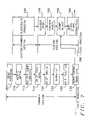
- FIG. 2shows a process for forming integrated circuit modules.
- the processbegins with the formation 200 of the integrated circuit chip on a semiconductor wafer.
- the semiconductor process 210forms the collection of transistors that are the electronic circuits on the semiconductor wafer.
- the electronic circuitsare interconnected by metalization and are also connected to input/output pads by the metalization placed on the surface of the semiconductor wafer.
- optional functionsmay be personalized to select optional functions.
- the fuses 150 a , 150 b , and 150 care either opened or held intact during this process to select the desired input/output organization options.
- An alternative to selecting the desired input/output organization options of the DRAM of FIG. 1is exposing the metalization on the surface of the semiconductor substrate that forms the fuses 150 a , 150 b , and 150 c to intense laser light to destroy the appropriate fuses 150 a , 150 b , and 150 c.
- the steps of formation of the integrated circuit chipis common for all the desired selectable functions until the metalization to select the desired functions.
- the integrated circuit chipsthen becomes a custom design.
- the integrated circuit chiphas a common design until the destruction of fuses to create the custom personalization that selects each desired function of the integrated circuit chip.
- the semiconductor waferis placed on a test system and each integrated circuit chip is tested 215 for functionality.
- the functioning chipsare denoted as functional die.
- the semiconductor waferis then diced 220 and the functional die are separated for further assembly 225 in a first level or module package.
- the selection or omission of connections between the functional integrated circuit die and the first level packageis a custom design particular to each combination of desired functions.
- the input/output pads of the desired functions of the functional dieare connected by a method such as wire bonding or tape automated bonding to the pins of the first level package.
- the input/output pads of the undesired functionare omitted during the wire bonding or tape automated bonding.
- the packageis tested 230 and inventoried 235 for further assembly.
- the assembly 205 of the second level packagebegins by forming 240 the substrate of the second level assembly. Multiple layers substrate are formed having interconnection metalization that connects the packaged and tested die to external circuitry that is present either on the second level package or elsewhere within the electronic system. The multiple layers are assembled to form the substrate of the second level assembly.
- a solder maskis placed 245 on the second level assembly and a solder paste is placed 250 at all connection points of the packaged and tested die.
- the packaged and tested dieis attached 255 to the second level assembly.
- the solder pasteis melted and the pins of the packaged and tested die fused to the metalization of the second level assembly.
- the remaining processing of the second level assemblyis completed 260 .
- the metalization of the second level assemblymust be customized. Again, this increases the number of assembly types required to be inventoried.
- U.S. Pat. No. 5,360,992discloses a semiconductor package, which allows pinouts and bond options to be customized after encasement of a semiconductor die.
- the semiconductor packagehas two assemblies in a first embodiment and an optional third assembly in a second embodiment.
- a first assemblycomprises a semiconductor die encased in plastic, ceramic, or other suitable material. All available bond options (bond pads) are routed to the exterior portion of the package by a first assembly frame. Portions of the first assembly frame are exterior to the encasement and terminate in exterior pad portions that can be conductively bonded to.
- a second assembly of the inventioncomprises a second assembly frame that provides a means of input/output (I/O) between the packaged die and a next level of assembly onto which it is installed.
- the second assembly framecomprises conductive paths to which the exterior pad portions are connected, the first assembly being conductively mounted to the second assembly thereby.
- the frame of the second assemblydetermines the pinouts (the pin numbers associated with each of the signals of the device) of the various signals of the die contained within the first assembly.
- the optional third assemblywhich, if used, is interposed between the first and second assemblies, comprises means for “keying” the exterior pad portion desired locations or the second assembly frame.
- the assemblycan comprise at least two different forms.
- the third assemblyis a nonconductive membrane having voids there through, conductive paths of the second assembly are located in an “X” direction, while the exterior pad portions of first assembly of this form are bars extending in a “Y” direction.
- the pads of the first assemblycan either be connected with the conductive paths of the second assembly or isolated from the conductive paths if no void is formed.
- any of the bond optionscan be connected with any of the pinouts. Connecting is accomplished by coating the bars with a conductive material and interposing the insulative membrane between the first and second assemblies. The conductive material fills the voids, thereby passing signals between the first and second assemblies.
- the third assemblycomprises a flex circuit as used with tape automated bonding.
- the second assemblyhas a single design, and the layout of the flex circuit determines the pinouts and options of the semiconductor device.
- the flex circuitis conductively mounted to the first and second assemblies in a fashion consistent with tape automated bonding (TAB) technology, for instance with solder, or by some other means such as conductive epoxy.
- TABtape automated bonding
- a reconfigurable x-y RAM arraywhich includes a memory array comprised of a plurality of RAM cell columns.
- the RAM cell columnsare organized into a number of groups where the number of groups corresponds to the bit width of the memory.
- Each groupcontains an equal number of columns so that the number of columns in a group multi number of groups equals the total number of array.
- the number of columns in a groupis reconfigurable according to the present invention.
- the bit width of the memoryis reconfigurable by modifying the number of columns in a group, since the bit memory corresponds to the number of groups.
- the RAMdecodes an address and selects one bit from each column group.
- the word size stored by the RAMis determined by the number of columns groups configured in the array.
- Agrawal et al.provides multiplexer (mux) logic coupled to each column.
- Column select logicdecodes a memory address and provides select signals corresponding to the address to the mux logic.
- the muxselects a particular column in the group to be accessed and outputs a column bit signal indicative of the memory state of the selected column.
- Column configuration logicis coupled to the mux logic and combines the mux outputs into memory bit signals.
- the mux outputs combined by the column configuration logicdetermine the size of the column groups from which a memory bit signal is selected.
- the column configuration logicmay be placed in different modes to configure different column group sizes and thus to reconfigure the bit width of the memory.
- the column select logicis responsive to the configuration mode and decodes the address for the appropriate column group size.
- An object of this inventionis to provide integrated circuit modules having common known good integrated circuit die. Selectable functions of the known good integrated circuit die are chosen during packaging of the known good integrated circuit die. Such selectable functions allow a reduction of the variety of integrated circuit components during manufacturing and assembly. This provides a method to reduce the required inventory of integrated circuit components at integrated circuit manufacturers, distributors, and integrated circuit users.
- Another object of this inventionis a method of assembly of integrated circuit modules to choose selectable functions of known good integrated circuit die to be mounted in the integrated circuit modules.
- the integrated circuit modulehas a substrate of a first type an integrated circuit to be mounted to the module.
- the integrated circuithas multiple selectable input functions, multiple selectable output functions, common functions, a function selector, all are interconnected and connected to input/output pads.
- the substrate of the first typeis mounted to a substrate of a second type.
- the substrate second typehas wiring connections to the input/output pads of the substrate of the first type and thus to the integrated circuit that select desired input functions and output functions. Further, the wiring connections on the substrate of the second type provide signal paths to transfer signals to the desired input function and signals from the desired output function, and signals to and from the common functions. Also, the wiring connections form connections between the input/output pads and external circuitry.
- the substrate of the second typehas connector pins to provide physical and electrical connections between the external circuitry and the wiring connections on the substrate of the second type.
- the integrated circuitmay be a DRAM integrated circuit die.
- the DRAM integrated circuithas a plurality of selectable input/output organizations. Each of the selectable input/output organizations is selected as one of the logic states to the function selector and connections from the second level substrate to unused input/output function connected to input/output pads of the DRAM are omitted from the second level substrate.
- the integrated circuitmay be a common computational processor (a microprocessor, a microcontroller, a digital signal process, etc.).
- the common computational processorhas selectable input functions and selectable output functions that include analog-to-digital converters, digital-to-analog converters, general purpose word-width input/output buses, standard compliant serial interfaces, interfaces to host processors of a system, control signal inputs and outputs, timer/counter inputs and outputs, computer operating properly signals, and interrupt signals.
- the input/output pads of the substrate of the first typeare solder bumps, which are arranged as a ball grid array.
- the selectable input functions and the selectable output functionsare chosen by creating or omitting voids in a solder mask on the second level substrate during assembly. The desired connections are then made to the second level substrate and the undesired connections are omitted.
- the method to form an integrated circuit modulebegins by forming an integrated circuit die having multiple selectable input functions, multiple selectable output functions, common functions, and a selector function.
- the integrated circuit dieis created by forming electronic components on a surface of a semiconductor wafer to form the multiple selectable input functions, the multiple selectable output functions, common functions, and the selector function. Redistribution metallurgy is then formed on the surface of the semiconductor wafer to form input/output pads connected to the multiple selectable input functions, the multiple selectable output functions, the common functions, and the selector functions.
- the integrated circuit dieis then tested to determine functional integrated circuits die.
- the semiconductor waferis then diced to separate integrated circuit die are then burned-in, tested to find the known good integrated circuit die.
- the known good integrated circuit dieare then sorted and inventoried.
- the substrate of the second typeis created by forming metal interconnections on multiple layers of the substrate of the second type, and laminating of the multiple layers of the substrate of the second type.
- the integrated circuit moduleis then assembled by applying a solder mask to a component level of said substrate of the second type.
- the solder maskis applied to the substrate of the second type so as to have voids to expose the input/output pads of the common functions, desired functions of the multiple selectable input functions and the multiple selectable output functions, and the input/output pads that select the desired functions with input and output functions.
- solder maskwill have the voids omitted to eliminate the connections of the non-desired functions of the multiple selectable input functions, the multiple selectable output functions, and the selector function by coating the input/output pads of the non-desired functions.
- a solder pasteis deposited on the input/output pads exposed by the solder mask.
- the substrate of the first typeis then placed and secured to the component level of the second level substrate. The method is then completed with final assembly and test of the integrated circuit module.
- the substrate of the first typeis a semiconductor substrate or die onto which the integrated circuit is formed.
- the integrated circuit dieis mounted directly to the substrate of the second type.
- the input/output pads of the integrated circuit dieare either connected or not connected to the corresponding pads of the substrate of the second type to activate the desired functions of the integrated circuit.
- the substrate of the first typeis a substrate that is to provide a connective transformation of the input/output pads of the integrated circuit die and the metal interconnections of the substrate of the second type.
- the substrate of the first typeis created by forming metal connections that align with input/output pads of the integrated circuit die and extend to align with the connections points on the substrate of the second type.
- the integrated circuit dieis mounted and secured to the substrate of the first type.
- the substrate of the first type with the integrated circuit die mountedis then tested, optionally burned-in, sorted, and inventoried.
- the substrate of the first type with the mounted integrated circuit dieis then secured to the substrate of the second type.
- the substrate of the second typehas the desired metal connections made between the substrate of the first type and the substrate of the second type to select the preferred functions of the integrated circuit.
- FIG. 1is a schematic diagram of a DRAM illustrating the configuring circuitry of the prior art.
- FIG. 2is a flow chart illustrating the method of assembly of an integrated circuit chip on a second level assembly of the prior art.
- FIG. 3is a diagram of an integrated circuit package illustrating the configurability of a known good integrated circuit die having multiple selectable functions of the first embodiment of this invention.
- FIG. 4is a schematic diagram of a DRAM illustrating the configuring circuitry of this invention.
- FIGS. 5 a - 5 eare diagrams of an area array of input/output pads of a DRAM module illustrating the configurations of the data input/output pins of this invention.
- FIG. 6is a schematic diagram of a multiple selectable function computational processor illustrating the configuration structure of this invention.
- FIG. 7is a diagram of a flow chart illustrating the method of assembly of a known good integrated circuit die on a second level assembly of the first embodiment of this invention.
- FIG. 8is a diagram of an integrated circuit package illustrating the configurability of multiple a known good integrated circuit die having multiple selectable functions of this invention.
- FIG. 9is a diagram of an integrated circuit package illustrating the configurability of a known good integrated circuit die having multiple selectable functions of the second embodiment of this invention.
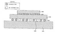
- FIG. 10is a cross sectional view of an integrated circuit package of the second embodiment of this invention.
- FIG. 11is a diagram of a flow chart illustrating the method of assembly of a known good integrated circuit die on a second level assembly of the second embodiment of this invention.
- a multiple selectable function integrated circuit die 300has a plurality of selectable input functions 306 and selectable output functions 308 and common functions 304 .
- the selectable input functions 306are circuits that implement such functions as interface standard receivers, analog-to-digital converters, and address and control decoders.
- the selectable output functions 308are circuits that implement such functions as interface standard drivers, digital-to-analog converters, address drivers, data drivers, control drivers, and timing signal drivers.
- the common functions 304are circuits that implement such functions as DRAM array address and support functions, SRAM array address and support functions, non-volatile memory array address and support functions, computational processor circuitry such as arithmetic logic units and multiply accumulate function, program decoder circuits, timing circuits, and address generation.
- a select function 310is connected to the selectable input functions 306 , the selectable output functions 308 , and the common functions 304 by the internal input bus 374 , the internal output bus 372 , and the internal common bus 376 .
- the computational processormay be configured as a microprocessor, a microcontroller, a digital signal processor, or other complex logic function.
- the select function 310is based on the logic states of the select signals 378 , the common select signals 380 , output select signals 382 , the interconnections between the internal input bus 374 , the internal output bus 372 , and the internal common bus 376 . Any of the selectable input functions 306 , selectable output functions 308 , and common functions 304 that are not to be configured are effectively disabled and disconnected from those that are being configured for a given configuration of the integrated circuit module.
- connections to power supply voltage sources and to the ground reference pointsare required for the functioning of the known good integrated circuit die 300 and in fact may be connected or disconnected from the selectable input functions 306 or the selectable output functions 308 as part of the selection of these functions.
- the common input and the common output signals 386 and 388 that are common to all configurations of the integrated circuit moduleare introduced to the common input module connectors 336 and are received from the common output module connectors 336 .
- the common input module connectors 336have internal module wiring 390 connected to the common input module pads 334 .
- the common input module pads 334are connected 332 in a predetermined fashion to the common input pads 330 on the integrated circuit die 300 .
- input module pads 334are connected to the input pads 330 as wirebonds, tape automated bonds, and solder bumps of ball grid array.
- the common output module connectors 384have internal module wiring 398 connected to the common output module pads 340 .
- the common output module pads 340are connected 341 in a predetermined fashion to the common output pads 338 on the integrated circuit die 300 .
- output module pads 340are connected to the output pads 338 as wirebonds, tape automated bonds, and solder bumps of ball grid array.
- the common input signals 386 and the common output signals 388are typically, but not exclusively, timing control, and test stimulus signals.
- the selectable input function signals 312are introduced through the selectable input function module connectors 320 .
- the selectable input function module connectors 320are attached to the internal module wiring 392 , which is connected to the selectable input module pads 316 .
- the selectable input module pads 316 that will have desired selectable input function signals 312will be connected 318 to the selectable input/output pads 314 on the integrated circuit die 300 .
- the undesired selectable input function signalswill be omitted from the connections 318 between the selectable input module pads 316 and the selectable input pads 314 .
- the connections 318may be wire bonds, tape automated bonds, or solder bumps of a ball grid array.
- the selectable output function signals 394are transferred to external circuitry connected to the integrated circuit module on a second level of packaging through the selectable output function connectors 328 .
- the selectable output function connectors 328are attached to the integrated circuit module wiring 396 to the selectable output function module pads 324 .
- the desired selectable output function signals 394are transferred from the desired output function 308 to the output pads 322 on the integrated circuit die 300 .
- the desired output pads 322are connected to the corresponding selectable output function module pads 324 and thus to the selectable output function module connectors 328 .
- the undesired output function signals 394 on the output pads 322are omitted from connection to the selectable output function module pads 324 .
- the input function select signal 378 , the common function select signals 380 , and the output function select signals 382are transferred from external circuitry respectively through the input option select module connectors 348 , the common option select module connectors 356 , and the output option select module connectors 364 .
- the input option select module connectors 348 , the common option select module connectors 356 and output option select module connectors 364are respectively connected through module interconnecting wire to the input option select module pads 354 , the common option select module pads 344 , and the output option select module pads 362 .
- the input function select signals 378 , the common function select signals 380 , and the output function select signals 382are logic states established by either the power supply voltage source Vdd for a logic state of 1 or a ground reference voltage GND for a logic state of 0.
- the input/output pads 342 , 350 , 358 of the integrated circuit die 300are connected appropriately 346 , 352 , 360 to the input option select module pads 354 , the common option select module pads 344 , and the output option select module pads 362 .
- the input/output pads 342 , 350 , 358 of the integrated circuit die 300are appropriately omitted from the connections 346 , 352 , 360 to the input option select module pads 354 , the common option select module pads 344 and the output option select module pads 362 .
- One technique for implementing the selection of the multiple selectable functions of the integrated circuit die 300is to place the input/output pads 314 , 322 , 330 , 338 , 342 , 350 , 358 as an array of connecting pads on the surface of the known good integrated circuit die 300 .
- a solder bumpis applied to each of the input/output pads 314 , 322 , 330 , 338 , 342 , 350 , 358 in a structure of a ball grid array.
- the desired functions of the multiple selectable input functionsare “gang-bonded” to the module pads 316 , 324 , 334 , 340 , 344 , 354 , 362 . Since the formation of the input/output pads 314 , 322 , 330 , 338 , 342 , 350 , 358 is inherent in the processing of the wafer containing the multiple selectable function integrated circuit die 300 , there is no additional cost in forming the multiple selectable function integrated circuit die 300 . However, since only one design of the multiple selectable function integrated circuit die 300 is maintained, inventory is simplified and costs reduced.
- FIG. 4for an implementation of an embodiment of this invention as a DRAM having multiple input/output data width configurations.
- the structure and function of the DRAM array 100is as described in FIG. 1 .
- the internal data bus 110is connected to the input/output pad selector 425 .
- the data bus width of the internal data bus 110is at least the width of the widest data bit width configuration of input/output data bus 455 .
- the input functions 306 and the output function 308 of FIG. 3are combined in this embodiment as the data input/output functions 430 , 440 , and 450 .
- Datais received from or transferred to the DRAM module through the data connections 435 , 445 , and 455 .
- the data connections 435 , 445 , and 455are attached to each of the data input/output functions 430 , 440 , and 450 .
- each data input/output function 430 , 440 , and 450may share one or more of the data connections 435 , 445 , and 455 .
- the data input/output functions 430 , 440 , and 450establish the data bit width configurations and data connections, such as DQ 0 , are shared by all the data input/output functions.
- Each data connection DQ 0 , DQ 1 , . . . , DQnis connected to the input of a receiver 480 and the output of a driver 470 .
- the output of the receiver 480is the input of the demultiplexer 475 .
- Each output of the demultiplexer 475is connected to the input/output selector 425 and through the input/output selector 425 to the internal data bus 110 .
- the demultiplexer 475collects singularly, a number of data bits equivalent to the number of bits for the internal data bus 110 , and transfers them through the input/output selector 425 .
- the internal data bus 110is connected to the inputs of the multiplexer 465 .
- the output of the multiplexer 465is the input of the driver 470 .
- the output of the driver 470is connected to one of the data connections DQ 0 , DQ 1 , . . . , DQn.
- the multiplexer 465collects a number of data bits from internal data bus 110 through the input/output selector 425 and serialize these data bits for transfer to the one data connection.
- Each of the data input/output functions 430 , 440 , and 450is comprised of at least one set of the receivers 480 , drivers 470 , multiplexers 465 , and demultiplexers 475 connected to one of the data connections DQ 0 , DQ 1 , . . . , DQn.
- Thisallows the configurations of the input/output data buses 435 , 445 , and 455 to be varied as desired.
- a single DRAM array designcan be configured with any desired bit data width.
- the input/output selector 425selects which of the input/output functions 430 , 440 , and 450 that are to be configured within a package.
- the select inputs 460 of the input/output selector 425provide the appropriate logic states to select the desired input/output configuration or which of the input/output functions 430 , 440 , and 450 are to be implemented.
- the select inputs 460are connected to the option decoder 420 .
- the option decoder 420is connected to the option receivers 425 which, in turn, are connected to the option select connections 410 .
- the DRAM integrated circuit dieis processed and tested as described above and the known good die are inventoried. Mounting the known good DRAM die on a second level package such as a “chip-on-chip” structure, a ceramic module, a plastic package, a fiberglass reinforced plastic printed circuit card, or an insulator coated metal selects the desired optional configuration for the DRAM module.
- a second level packagesuch as a “chip-on-chip” structure, a ceramic module, a plastic package, a fiberglass reinforced plastic printed circuit card, or an insulator coated metal selects the desired optional configuration for the DRAM module.
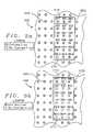
- the known good DRAM die of FIG. 4has its input/output connections implemented as an array 505 of solder bumps on the surface 500 of the known good DRAM die.
- the selectable data input/output connections 510 and the option select connections 515are placed conveniently on the surface of the known good DRAM die. In this instance, it is an area of three columns and six rows.
- This implementation as shownis for a DRAM having optional organization .times.1 (by one), .times.4 (by four), .times.8 (by eight), and .times.16 (by 16). That is there are four input/output functions requiring two option select connections Op 1 and OP 2 .
- the .times.1 optionactivates only the input/output function connected to the selectable data input/output connection DQ 0 .
- the .times.4 optionactivates the input/output functions connected to the selectable data input/output connections DQ 0 , DQ 1 , DQ 2 , and DQ 3 .
- the .times.8 optionactivates the input/output functions connected to the selectable data input/output connections DQ 0 , DQ 1 , . . . , and DQ 8 .
- the .times.16 optionactivates the input/output functions connected to the selectable data input/output connections DQ 0 , DQ 1 , . . . , and DQ 15 .
- FIG. 5 billustrates the implementation of the .times.1 organization.
- the option select connections 515are made between the known good DRAM die and the second level package to connect to the necessary logic states to activate the .times.1 option.
- the DQ 0 input/output connection of the selectable data input/output connections 520is made to the second level package for transfer of digital signals.
- the remaining selectable data input/output connections DQ 1 , DQ 2 , . . . , DQ 15 520are masked and the solder balls are not allowed to connect to the interconnecting wiring of the second level substrate.
- FIG. 5 cis a .times.4 organization.
- the input/output functionis selected by the option select connection OP 1 being connected to the second level package to place the appropriate logic states at the option desired.
- the option select connection OP 2is omitted from being made.
- the selectable data input/output connections DQ 0 , DQ 4 , DQ 8 , and DQ 12 of the input/output connections 520are connected to the second level package.
- FIG. 5 dis a .times.8 organization.
- the input/output functionis selected by connecting the option select connection OP 2 and omitting the connection of the option select connection Op 1 from the second level package to place the appropriate logic state at the option decoder.
- the selectable data input/output connections DQ 0 , DQ 2 , DQ 4 , DQ 6 , DQ 8 , DQ 10 , DQ 12 , and DQ 14are affixed to the second level package and the selectable data input/output connections DQ 1 , DQ 3 , DQ 5 , DQ 7 , DQ 9 , DQ 11 , DQ 13 and DQ 15 are omitted from the second level package.
- the .times.16 option of the known good DRAM dieis shown in FIG. 5 e .
- the .times.16 optionis selected by omitting the option select connections Op 1 and OP 2 from the second level package to place the appropriate logic state at the option decoder. All of the selectable data input/output connections 520 are joined to the second level package.
- the wiring connections of the second level package onto which the known good DRAM die is mountedcan have those wiring tracks to implement all options.
- the masking stage of the module assembly and the placement of the solder pastedetermine the option implementation of the DRAM module.
- the interconnection pads that will accept the selectable data input/output connections 520may be omitted and any unnecessary wiring tracks on the second level package may be omitted. This allows routing of wiring tracks of the external circuitry on the second level module to change common computational die to selectable function computational die.
- a digital computational processor modulehas selectable functions to a common computational die 600 to be configured during mounting to a second level package according to desired optional functions.
- the optional functionconfigures the common computational die as a general-purpose microprocessor, a special function microprocessor, a microcontroller, or a digital signal processor.
- the common computational die 600has selectable input functions and selectable output functions 605 that include analog-to-digital converters, digital-to-analog converters, general purpose word-width input/output buses, standard compliant serial interfaces, interfaces to host processors of a system, control signal inputs and outputs, timer/counter inputs and outputs, computer operating properly signals, and interrupt signals.
- the selectable function computational diehas common input functions and common output functions 615 such as a test interface to provide test stimuli and response for the digital computational module. Other selectable input and output functions 635 will be the address, data, and control functions to interface to external memory array.
- the internal structure of the selectable function computational die 600includes certain functions of the computational processor 620 .
- Common functionsare functions like program and control decoder logic 621 and address generation logic 622 .
- the selectable functionsare the data arithmetic/logic unit 623 and the digital signal processing multiply accumulate unit 624 .
- Other internal selectable functions 625are the internal program and data memory and the internal timing circuits.
- the selectable input and output functions 605 , 635 , the common input and output functions 615 , the internal selectable functions 625 , and the computational processor 620are interconnected with the data and control bus 630 .
- the option select signals 640provide the appropriate logic states to function select circuit 610 to determine the desired functions of selectable function computational die 600 .
- the function select circuitis connected to the selectable input and output functions 605 and 635 , the internal selectable functions 625 , and the selectable functions of the computational processor 620 through the selector bus 645 .
- the second level packageprovides the logic states for the option select signals 640 and will make the connections to the desired functions of the selectable function computational die 600 .
- the undesired functions on the selectable function computational die 600are omitted in the mounting of the selectable function computational die from the second level package.
- a multiple selectable function integrated circuit dieis formed 700 on a semiconductor wafer by formation and interconnection of electronic circuits on the semiconductor wafer employing known semiconductor processes. Redistribution metal is fabricated 705 on the surface of the semiconductor wafer forming the connections of the common internal functions and the selectable internal functions of the multiple selectable function integrated circuit die to input/output pads on the surface of the semiconductor wafer. The solder bumps are then formed and reflowed to form 710 the solder ball on the surface of the semiconductor wafer. The individual multiple selectable function integrated circuit dies are then tested 715 and the functional multiple selectable function integrated circuit dies are identified.
- the semiconductor waferis then diced 720 and the functional multiple selectable integrated circuit die are burned-in 725 to eliminate any early life failures of the functional multiple selectable function integrated circuit dies.
- the functional multiple selectable function integrated circuit diesare then tested 730 and the known good multiple selectable function integrated circuit die are sorted 735 , with the non-functioning die discarded.
- the forming 700 of the known good multiple selectable function integrated circuit diesallows a single common design to be inventoried.
- the second level package module substrateis formed 740 by applying and forming metal interconnection on substrate laminates of the second level package substrate.
- the laminatesare bonded together to create the second level package substrate.
- the wiring connections on the second level package substratemay either be custom for each option selection of the multiple selectable function integrated circuit or have a common design to minimize inventory of the different option designs.
- a solder maskis placed 745 on the second level package substrate.
- the solder maskwill expose the desired interconnecting pads of the metal interconnections on the second level package substrate to implement the desired functional options of the multiple selectable function integrated circuit die.
- Those undesired functionshave no voids in the solder mask to prevent exposure of the metal connections to prevent connection to the input/output pads of the undesired functions of the multiple selectable function integrated circuit dies.
- Solder pasteis applied 750 to make contact with the desired interconnecting pads of the metal interconnections on the second level package substrate.
- the known good multiple selectable function integrated circuit dieare then secured 755 to the second level package substrate to form the connections between the desired functions of the multiple selectable function integrated circuit die and external circuitry through the metal interconnections on the second level package substrate.
- the second level package substrateis processed 755 through final assembly and test and is ready for further system level construction. Since the final assembly is the “gang-bonding” as in what is known in the art as “flip chip assembly”, no extra cost is incurred to have the ability to select multiple functions during system and subsystem assembly.
- the second level package substratemay be a ceramic substrate, a plastic substrate, a fiberglass reinforced substrate, a metal substrate having layers of insulative material to isolate the metal interconnections, semiconductor substrates, a glass substrate, or an integrated circuit die to form a chip-on-chip structure.
- FIG. 8illustrates a packaging structure 800 where more than one multiple selectable function integrated circuit die 805 and 810 are connected together to form a more complex subsystem having selectable interconnecting functions.
- the multiple selectable function integrated circuit die 805 and 810are structured as described in FIG. 3 .
- the selectable functions of the first multiple selectable function integrated circuit die 805differ from those of the second multiple selectable function integrated circuit die 810 .
- selectable input functions and selectable output functions of FIG. 3are represented jointly as the selectable input/output functions 805 a , 805 b , 810 a , and 810 b .
- Certain selectable input/output functions 805 a and 810 aare connected through the selectable input/output function connectors 825 and 840 to circuitry external to the illustrated packaging structure 800 .
- Other selectable input/output functions 805 b and 810 bare appropriately interconnected through the selectable input/output connectors 815 .
- the common functions 805 c and 810 care connected to the circuitry external to the illustrated packaging structure 800 through the common function connectors 830 and 845 .
- the common functions 805 c of the first multiple selectable function integrated circuit die 805are interconnected through the common function connectors 820 to the common functions 810 c of the second multiple selectable function integrated circuit die 810 .
- the option select signals 835 and 850are each an aggregate of the option select signals of FIG. 3 .
- the option select signals 835are connected to the option selector 805 d of the first multiple selectable function integrated circuit die 805
- the option select signals 850are connected to the option selector 810 d of the second multiple selectable function integrated circuit die 810 .
- the selectable input/output functions 805 a , 805 b , 810 a , and 810 bare chosen by application of the appropriate logic state to the option selectors 805 d and 810 d . This is accomplished by selectively connecting or omitting connections of the option select signals 835 and 850 respectively to the options selectors 805 d and 810 d . Further, those desired selectable input/output connectors 815 , 825 , and 840 are established during the attaching of the first and second multiple selectable function integrated circuit die 805 and 810 to a second level package assembly. The undesired selectable input/output connectors 815 , 825 , and 840 are omitted during the attaching as described above.
- the first and second multiple selectable function integrated circuit die 805 and 810may each be a DRAM, a computational processor (microprocessor, a microcontroller, a digital signal processor, etc.), or other logic or analog functional integrated circuit die. Additionally, the first multiple selectable function integrated circuit die 805 may be attached to the second multiple selectable function integrated circuit die 810 . Conversely, the second multiple selectable function integrated circuit die 810 may be attached to the first multiple selectable function integrated circuit die 805 . Further, the first multiple selectable function integrated circuit die 805 and the second multiple selectable function integrated circuit die 810 may mounted one to another in a “chip-on-chip” structure. An example of the above would be the mounting of a DRAM known good integrated circuit die as the first multiple selectable function integrated circuit die 805 to a complex logic function as the second multiple selectable function integrated circuit die 810 .
- the minimum spacing allowed for the second level or system level packagingis often larger than the maximum spacing desired for the input/output pads of an integrated circuit.
- a module or first level packagingis interposed between the integrated circuit and the second level packaging.
- the first level packagingacts as an interconnection adapter to connect the input/output pads of the integrated circuit with the pin or interconnection pads of the second level package.
- the integrated circuit chipis mounted to the first level package with connections to the wiring of the first level packaging.
- the wiring of the first level packagingprovides a direct one-to-one connection for each input/output pad of the integrated circuit to the interconnection pads of the second level package with no circuit characterization provided in the first level package.
- the first level packageis thus provides a spatial transform between the integrated circuit chip and the second level package.
- the integrated circuit 300is designed and fabricated as described in FIG. 3 . However instead of being place directly on a module that is effectively the second level or system package, the integrated circuit 300 is mounted and secured to the first level or module package 900 .
- the input/output pads 314 , 322 , 330 , 338 , 342 , 350 , and 358are respectively connected to the interconnection pads 918 , 958 , 932 , 954 , 946 , 966 , and 974 of the first level package 900 respectively by the connections 916 , 960 , 931 , 953 , 948 , 968 , and 976 .
- the connections 916 , 960 , 931 , 953 , 948 , 968 , and 976are permanently established when the integrated circuit 300 is mounted and secured to the first level package 900 .
- the first level package 900in effect, becomes a space transform to transform the maximum spacings allowed of the integrated circuit 300 to the minimum spacings allowed by the second level package 302 .
- the interconnection pads 918 , 958 , 932 , 954 , 946 , 966 , and 974 of the first level package 900have dimensions and spacings to facilitate connection with the input output pads 314 , 322 , 330 , 338 , 342 , 350 , and 358 of the integrated circuit chip 300 .
- the first level package 900must have interconnection pads or pins 922 , 962 , 936 , 956 , 950 , 970 , and 978 that attach to the second level package 302 .
- the interconnection pads 922 , 962 , 936 , 956 , 950 , 970 , and 978are respectively connected to the interconnection pads 918 , 958 , 932 , 954 , 946 , 966 , and 974 by the wiring connections 920 , 960 , 934 , 955 , 948 , 968 , and 976 of the first level package 900 .
- the common input and the common output signals 386 and 388 that are common to all configurations of the integrated circuit moduleare introduced to the common input module connectors 336 and are received from the common output module connectors 338 .
- the common input module connectors 336are connected to the common input pads 330 in a predetermined fashion by way of the connection 938 to the interconnection pads 936 of the first level package 900 .
- the common output module pads 340are connected 957 in a predetermined fashion to the common output pads of the common output signals 384 on the second level package by way of the interconnection pads 956 of the first level package 900 .
- the selectable input function signals 312are introduced through the selectable input function module connectors 320 .
- the selectable input function module connectors 320are selectably connected by the connections 924 to the interconnection pads 922 and thus to the input/output pads 314 of the integrated circuit.
- the undesired selectable input function signals 906will be omitted from the connections 924 between the interconnection pads 922 of the first level package and selectable input function module connectors 320 .
- the selectable output function signals 394are transferred to external circuitry connected to the integrated circuit module on a second level of packaging through the selectable output function connectors 328 .
- the selectable output function connectors 328are attached to the first level package by the connections 964 to the interconnection pads 962 of the first level package.
- the desired selectable output function signals 394are transferred from the desired output function 308 to the output pads 322 and thus to the interconnection pads 962 .
- the interconnection pads 962 and thus desired output pads 322are connected to the selectable output function module connectors 328 .
- the undesired output function signals 394 on the output pads 322are omitted from connection to the selectable output interconnection pads 962 .
- the input function select signal 378 , the common function select signals 380 , and the output function select signals 382are transferred from external circuitry respectively through the input option select module connectors 348 , the common option select module connectors 356 , and the output option select module connectors 364 .
- the input option select module connectors 348 , the common option select module connectors 356 and output option select module connectors 364are respectively connected through interconnection pads 950 , 970 , and 978 .
- the input function select signals 378 , the common function select signals 380 , and the output function select signals 382are logic states established by either the power supply voltage source Vdd for a logic state of 1 or a ground reference voltage GND for a logic state of 0.
- the input option select module connectors 348 , the common option select module connectors 356 , and the output option select module connectors 364are selectively attached to the interconnection pads 950 , 970 , and 978 by way of the connections 952 , 972 and 980 .
- the integrated circuit die 300is mounted to the first level package 900 by the solder balls or solder bumps 902 .
- An alternative attachmentmay be with a Tape Automated Bond or wirebond as described above. All the input/output pads of the integrated circuit die 300 are connected through the solder bumps 902 to the first level package 900 .
- the first level package 900is mounted to the second level package 302 with the solder balls 904 . To configure the function of the integrated circuit die 300 , the solder balls 904 are connected or omitted 906 as desired.
- the desired functions of the multiple selectable functionsare “gang-bonded” to the interconnection pads 922 , 962 , 936 , 956 , 950 , 970 , and 978 . Since the formation of the interconnection pads 922 , 962 , 936 , 956 , 950 , 970 , and 978 is inherent in the processing of the first level package 900 , there is no additional cost in forming the multiple selectable function integrated circuit die 300 and the first level module 900 . However, since only one design of the multiple selectable function integrated circuit die 300 mounted on the first level package 900 is maintained, inventory is simplified and costs reduced.
- the solder balls 904 of the implementationare illustrative of the concept of this invention.
- the connection of the first level package 900 to the second level package 302may be made by a lead frame having pins that are placed in holes drilled into the second level package 302 , as in a dual in-line package (Dual In-Line Package (DIP), Single In-Line Package (SIP), Zig-Zag In-Line Package (ZIP)).
- DIPDual In-Line Package
- SIPSingle In-Line Package
- ZIPZig-Zag In-Line Package
- the pinsmay be brazed or otherwise affixed to the first level package 900 as in a so-called pin grid array (PGA).
- PGApin grid array
- the lead framemay also have surface mounted pins that are constructed to be attached to the surface of the second level package 302 as with the leadless and leaded chip carriers (small outline J-leaded chip carriers (SOJ), plastic leadless chip carriers (PLCC), and quad-flat packs (QFP), etc.).
- SOJsmall outline J-leaded chip carriers
- PLCCplastic leadless chip carriers
- QFPquad-flat packs
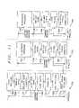
- FIG. 11for a discussion of the assembling and selecting the desired options of the multiple selectable functions integrated circuit of the second embodiment.
- the processing 790 of the integrated circuit die 300 of FIG. 9proceeds as described in FIG. 7 except in this embodiment subsequent to the sorting 790 of the known good die the integrated circuit die 300 is mounted on the first level package 900 .
- the processing 792 of first level packagebegins with the first level package module substrate being formed 765 by applying and forming metal interconnection on substrate laminates of the first level package substrate.
- the laminatesare bonded together to create the first level package substrate.
- the wiring connections on the first level package substratehave a common design to minimize inventory of the different option designs.
- a solder maskis placed 770 on the first level package substrate.
- the solder maskexposes the interconnecting pads of the metal interconnections on the first level package substrate to permit connections of the input/output pads of the multiple selectable function integrated circuit die.
- Solder pasteis applied 775 to make contact with the interconnecting pads of the metal interconnections on the first level package substrate.
- the known good multiple selectable function integrated circuit dieare then secured 780 to the first level package substrate to form the connections between the desired functions of the multiple selectable function integrated circuit die and external circuitry through the metal interconnections on the first level package substrate.
- the first level package substrateis processed 785 through final assembly and test and is ready for further system level construction. Since the final assembly is the “gang-bonding” as in what is known in the art as “flip chip assembly”, no extra cost is incurred to have the ability to select multiple functions during system and subsystem assembly.
- the second level process 796is executed as described in FIG. 7 except that instead of the integrated circuit die being mounted to the second level package, the first level package as described above is the component placed 755 on the second level package.
- first and second level package substratesmay be a ceramic substrate, a plastic substrate, a fiberglass reinforced substrate, a metal substrate having layers of insulative material to isolate the metal interconnections, semiconductor substrates, a glass substrate, or an integrated circuit die to form a chip-on-chip structure.
Landscapes
- Engineering & Computer Science (AREA)
- Computer Hardware Design (AREA)
- Microelectronics & Electronic Packaging (AREA)
- Power Engineering (AREA)
- Manufacturing & Machinery (AREA)
- Physics & Mathematics (AREA)
- Condensed Matter Physics & Semiconductors (AREA)
- General Physics & Mathematics (AREA)
- Semiconductor Integrated Circuits (AREA)
- Dram (AREA)
- Design And Manufacture Of Integrated Circuits (AREA)
Abstract
Description
- This application is a continuation of application Ser. No. 11/181,175, filed on Jul. 14, 2005, now pending, which is a Continuation-in-Part of U.S. patent application Ser. No. 09/246,303, filing date Feb. 8, 1999, now issued as U.S. Pat. No. 6,356,958.
- This application is related to the U.S. patent application Ser. No. 09/258,911, filing date Mar. 1, 1999, now U.S. Pat. No. 6,180,426 B1, issued Jan. 30, 2001.
- 1. Field of the Invention
- This invention is related to integrated circuits. More particularly, this invention relates to multiple function integrated circuits such as Dynamic Random Access Memories (DRAM) having function selection through wiring connections on a second level substrate onto which an integrated circuit is mounted.
- 2. Background of the Related Art
- The structure of a DRAM is well known in the art. Usually a DRAM chip is configured to be organized as a .times.1 (by 1), .times.4 (by 4), .times.8 (by 8), or .times.16 (by 16) package by selective destruction of fuses internal to the DRAM chip and by selectively connecting the data input/output pads to pins on a package. The unused pins are not connected to the input/output pads of the undesired or unused data transfer pads. Refer now to
FIG. 1 for a schematic drawing of the structure of a DRAM integrated circuit showing the input/output selection function. ADRAM array 100 has multiple banks of arrays of DRAM cells. Address signals are applied to the address I/O's105 and decoded within column address and row address decoders to select DRAM cells within theDRAM array 100. - Control and
timing signals 120 are applied to the control logic andtiming generator 115 to provide the necessary control and timing functions for theDRAM array 100. - Upon applying an address to the
DRAM array 100, digital data is transferred to or from theDRAM array 100 by theinternal data bus 110. Theinternal data bus 110 is connected between the sense amplifier and I/O bus on each memory bank. Theinternal data bus 110 may conceptually have a connection for each column of one memory bank, but usually is the maximum data bit width configuration of the DRAM integrated circuit. - The
internal data bus 110 is connected to the input/output selector 125. The input/output selector 115 determines the interconnections between the input/output buffers 130 and theinternal data bus 110. Theselection pins 140 of the input/output selector 125 are connected to the selection networks formed of theresistors fuses selection pins 140, if afuse selection pins 140, if afuse selection pins 140 determine which connections on theinternal data bus 110 are connected to which of the input/output buffers 130. While, as shown, the selector circuits will draw unacceptable amounts of standby current, it is presented here for illustration. Other techniques known in the art are used to form the selection networks. - The input/
output buffers 130 are connected to thepads 135. Thefuses fuses - Those input/
output pads 135 not used for a configuration are not connected to the module connections during the next level assembly. The fused configuration selection forces the maintenance of inventory of the DRAM die for each desired configuration increasing the difficulty in planning of production of DRAM wafers. - While the structure of the prior art as shown in
FIG. 1 is described for a DRAM, other integrated circuit functions such as computational processors (microprocessors, microcontrollers, digital signal processors, etc.), programmable memory, and programmable logic arrays employ metal masking or fuse destruction at the wafer level, and making or omitting connections during attachment of the functional integrated circuit die to a next level package assembly. This complicates the semiconductor processing in that extra masking steps are required for mask programming of desired functions of the functional integrated circuit die. Each function desired requires a unique mask for the selection process, further complicating the semiconductor process. Additionally, fuse destruction adds an extra step in the processing of the functional integrated circuit die. FIG. 2 shows a process for forming integrated circuit modules. The process begins with theformation 200 of the integrated circuit chip on a semiconductor wafer. The semiconductor process210 forms the collection of transistors that are the electronic circuits on the semiconductor wafer. The electronic circuits are interconnected by metalization and are also connected to input/output pads by the metalization placed on the surface of the semiconductor wafer. During the metalization, optional functions may be personalized to select optional functions. In the case of the DRAM ofFIG. 1 , thefuses FIG. 1 is exposing the metalization on the surface of the semiconductor substrate that forms thefuses appropriate fuses - The steps of formation of the integrated circuit chip is common for all the desired selectable functions until the metalization to select the desired functions. The integrated circuit chips then becomes a custom design. Equally, the integrated circuit chip has a common design until the destruction of fuses to create the custom personalization that selects each desired function of the integrated circuit chip.
- The semiconductor wafer is placed on a test system and each integrated circuit chip is tested215 for functionality. The functioning chips are denoted as functional die. The semiconductor wafer is then diced220 and the functional die are separated for
further assembly 225 in a first level or module package. The selection or omission of connections between the functional integrated circuit die and the first level package is a custom design particular to each combination of desired functions. - The input/output pads of the desired functions of the functional die are connected by a method such as wire bonding or tape automated bonding to the pins of the first level package. The input/output pads of the undesired function are omitted during the wire bonding or tape automated bonding. The package is tested230 and inventoried235 for further assembly.
- The
assembly 205 of the second level package begins by forming240 the substrate of the second level assembly. Multiple layers substrate are formed having interconnection metalization that connects the packaged and tested die to external circuitry that is present either on the second level package or elsewhere within the electronic system. The multiple layers are assembled to form the substrate of the second level assembly. - A solder mask is placed245 on the second level assembly and a solder paste is placed250 at all connection points of the packaged and tested die. The packaged and tested die is attached255 to the second level assembly. In a surface mounted packaging system, the solder paste is melted and the pins of the packaged and tested die fused to the metalization of the second level assembly. The remaining processing of the second level assembly is completed260.
- For integrated circuit modules having multiple functions, the metalization of the second level assembly must be customized. Again, this increases the number of assembly types required to be inventoried.
- U.S. Pat. No. 5,360,992 (Lowery et al.) discloses a semiconductor package, which allows pinouts and bond options to be customized after encasement of a semiconductor die. The semiconductor package has two assemblies in a first embodiment and an optional third assembly in a second embodiment.
- A first assembly comprises a semiconductor die encased in plastic, ceramic, or other suitable material. All available bond options (bond pads) are routed to the exterior portion of the package by a first assembly frame. Portions of the first assembly frame are exterior to the encasement and terminate in exterior pad portions that can be conductively bonded to.
- A second assembly of the invention comprises a second assembly frame that provides a means of input/output (I/O) between the packaged die and a next level of assembly onto which it is installed. The second assembly frame comprises conductive paths to which the exterior pad portions are connected, the first assembly being conductively mounted to the second assembly thereby. With the two-piece embodiment of the invention, the frame of the second assembly determines the pinouts (the pin numbers associated with each of the signals of the device) of the various signals of the die contained within the first assembly.
- The optional third assembly, which, if used, is interposed between the first and second assemblies, comprises means for “keying” the exterior pad portion desired locations or the second assembly frame. The assembly can comprise at least two different forms.
- In the first form, the third assembly is a nonconductive membrane having voids there through, conductive paths of the second assembly are located in an “X” direction, while the exterior pad portions of first assembly of this form are bars extending in a “Y” direction. By selectively placing the voids in the membrane, the pads of the first assembly can either be connected with the conductive paths of the second assembly or isolated from the conductive paths if no void is formed. Using the X-Y arrangement, any of the bond options can be connected with any of the pinouts. Connecting is accomplished by coating the bars with a conductive material and interposing the insulative membrane between the first and second assemblies. The conductive material fills the voids, thereby passing signals between the first and second assemblies.
- In the second form, the third assembly comprises a flex circuit as used with tape automated bonding. The second assembly has a single design, and the layout of the flex circuit determines the pinouts and options of the semiconductor device. The flex circuit is conductively mounted to the first and second assemblies in a fashion consistent with tape automated bonding (TAB) technology, for instance with solder, or by some other means such as conductive epoxy.
- U.S. Pat. No. 5,737,767 (Agrawal et al.) teaches a random access memory (RAM) array with a reconfigurable bit width or word width. In one embodiment, a reconfigurable x-y RAM array is provided which includes a memory array comprised of a plurality of RAM cell columns. The RAM cell columns are organized into a number of groups where the number of groups corresponds to the bit width of the memory. Each group contains an equal number of columns so that the number of columns in a group multi number of groups equals the total number of array. The number of columns in a group is reconfigurable according to the present invention. Thus, when the number of columns in a group is smaller, the number of groups is larger and when the number of columns in a larger, the number of groups is smaller. Thus, the bit width of the memory is reconfigurable by modifying the number of columns in a group, since the bit memory corresponds to the number of groups.
- To access a word stored in the array, The RAM decodes an address and selects one bit from each column group. Thus, the word size stored by the RAM is determined by the number of columns groups configured in the array.
- Agrawal et al. provides multiplexer (mux) logic coupled to each column. Column select logic decodes a memory address and provides select signals corresponding to the address to the mux logic. The mux selects a particular column in the group to be accessed and outputs a column bit signal indicative of the memory state of the selected column.
- Column configuration logic is coupled to the mux logic and combines the mux outputs into memory bit signals. The mux outputs combined by the column configuration logic determine the size of the column groups from which a memory bit signal is selected. The column configuration logic may be placed in different modes to configure different column group sizes and thus to reconfigure the bit width of the memory. The column select logic is responsive to the configuration mode and decodes the address for the appropriate column group size.
- An object of this invention is to provide integrated circuit modules having common known good integrated circuit die. Selectable functions of the known good integrated circuit die are chosen during packaging of the known good integrated circuit die. Such selectable functions allow a reduction of the variety of integrated circuit components during manufacturing and assembly. This provides a method to reduce the required inventory of integrated circuit components at integrated circuit manufacturers, distributors, and integrated circuit users.
- Another object of this invention is a method of assembly of integrated circuit modules to choose selectable functions of known good integrated circuit die to be mounted in the integrated circuit modules.
- The integrated circuit module has a substrate of a first type an integrated circuit to be mounted to the module. The integrated circuit has multiple selectable input functions, multiple selectable output functions, common functions, a function selector, all are interconnected and connected to input/output pads. The substrate of the first type is mounted to a substrate of a second type. The substrate second type has wiring connections to the input/output pads of the substrate of the first type and thus to the integrated circuit that select desired input functions and output functions. Further, the wiring connections on the substrate of the second type provide signal paths to transfer signals to the desired input function and signals from the desired output function, and signals to and from the common functions. Also, the wiring connections form connections between the input/output pads and external circuitry. To select the desired input functions and the desired output functions, appropriate logic states are applied to input/output pads connected to the function selector to configure a functional operation of the integrated circuit. The substrate of the second type has connector pins to provide physical and electrical connections between the external circuitry and the wiring connections on the substrate of the second type.
- The integrated circuit may be a DRAM integrated circuit die. The DRAM integrated circuit has a plurality of selectable input/output organizations. Each of the selectable input/output organizations is selected as one of the logic states to the function selector and connections from the second level substrate to unused input/output function connected to input/output pads of the DRAM are omitted from the second level substrate.
- The integrated circuit may be a common computational processor (a microprocessor, a microcontroller, a digital signal process, etc.). The common computational processor has selectable input functions and selectable output functions that include analog-to-digital converters, digital-to-analog converters, general purpose word-width input/output buses, standard compliant serial interfaces, interfaces to host processors of a system, control signal inputs and outputs, timer/counter inputs and outputs, computer operating properly signals, and interrupt signals.
- In one implementation of the integrated circuit module, the input/output pads of the substrate of the first type are solder bumps, which are arranged as a ball grid array. The selectable input functions and the selectable output functions are chosen by creating or omitting voids in a solder mask on the second level substrate during assembly. The desired connections are then made to the second level substrate and the undesired connections are omitted.
- The method to form an integrated circuit module begins by forming an integrated circuit die having multiple selectable input functions, multiple selectable output functions, common functions, and a selector function. The integrated circuit die is created by forming electronic components on a surface of a semiconductor wafer to form the multiple selectable input functions, the multiple selectable output functions, common functions, and the selector function. Redistribution metallurgy is then formed on the surface of the semiconductor wafer to form input/output pads connected to the multiple selectable input functions, the multiple selectable output functions, the common functions, and the selector functions. The integrated circuit die is then tested to determine functional integrated circuits die. The semiconductor wafer is then diced to separate integrated circuit die are then burned-in, tested to find the known good integrated circuit die. The known good integrated circuit die are then sorted and inventoried.
- The substrate of the second type is created by forming metal interconnections on multiple layers of the substrate of the second type, and laminating of the multiple layers of the substrate of the second type. The integrated circuit module is then assembled by applying a solder mask to a component level of said substrate of the second type. The solder mask is applied to the substrate of the second type so as to have voids to expose the input/output pads of the common functions, desired functions of the multiple selectable input functions and the multiple selectable output functions, and the input/output pads that select the desired functions with input and output functions. The solder mask will have the voids omitted to eliminate the connections of the non-desired functions of the multiple selectable input functions, the multiple selectable output functions, and the selector function by coating the input/output pads of the non-desired functions. A solder paste is deposited on the input/output pads exposed by the solder mask. The substrate of the first type is then placed and secured to the component level of the second level substrate. The method is then completed with final assembly and test of the integrated circuit module.
- In a first embodiment of the present invention, the substrate of the first type is a semiconductor substrate or die onto which the integrated circuit is formed. The integrated circuit die is mounted directly to the substrate of the second type. The input/output pads of the integrated circuit die are either connected or not connected to the corresponding pads of the substrate of the second type to activate the desired functions of the integrated circuit.
- In a second embodiment of the present invention, the substrate of the first type is a substrate that is to provide a connective transformation of the input/output pads of the integrated circuit die and the metal interconnections of the substrate of the second type. For the second embodiment, the substrate of the first type is created by forming metal connections that align with input/output pads of the integrated circuit die and extend to align with the connections points on the substrate of the second type. The integrated circuit die is mounted and secured to the substrate of the first type.
- The substrate of the first type with the integrated circuit die mounted is then tested, optionally burned-in, sorted, and inventoried.
- The substrate of the first type with the mounted integrated circuit die is then secured to the substrate of the second type. The substrate of the second type has the desired metal connections made between the substrate of the first type and the substrate of the second type to select the preferred functions of the integrated circuit.
FIG. 1 is a schematic diagram of a DRAM illustrating the configuring circuitry of the prior art.FIG. 2 is a flow chart illustrating the method of assembly of an integrated circuit chip on a second level assembly of the prior art.FIG. 3 is a diagram of an integrated circuit package illustrating the configurability of a known good integrated circuit die having multiple selectable functions of the first embodiment of this invention.FIG. 4 is a schematic diagram of a DRAM illustrating the configuring circuitry of this invention.FIGS. 5 a-5eare diagrams of an area array of input/output pads of a DRAM module illustrating the configurations of the data input/output pins of this invention.FIG. 6 is a schematic diagram of a multiple selectable function computational processor illustrating the configuration structure of this invention.FIG. 7 is a diagram of a flow chart illustrating the method of assembly of a known good integrated circuit die on a second level assembly of the first embodiment of this invention.FIG. 8 is a diagram of an integrated circuit package illustrating the configurability of multiple a known good integrated circuit die having multiple selectable functions of this invention.FIG. 9 is a diagram of an integrated circuit package illustrating the configurability of a known good integrated circuit die having multiple selectable functions of the second embodiment of this invention.FIG. 10 is a cross sectional view of an integrated circuit package of the second embodiment of this invention.FIG. 11 is a diagram of a flow chart illustrating the method of assembly of a known good integrated circuit die on a second level assembly of the second embodiment of this invention.- For a description of a general description of a general embodiment of this invention, refer now to
FIG. 3 . A multiple selectable function integrated circuit die300 has a plurality of selectable input functions306 andselectable output functions 308 andcommon functions 304. The selectable input functions306 are circuits that implement such functions as interface standard receivers, analog-to-digital converters, and address and control decoders. Theselectable output functions 308 are circuits that implement such functions as interface standard drivers, digital-to-analog converters, address drivers, data drivers, control drivers, and timing signal drivers. Thecommon functions 304 are circuits that implement such functions as DRAM array address and support functions, SRAM array address and support functions, non-volatile memory array address and support functions, computational processor circuitry such as arithmetic logic units and multiply accumulate function, program decoder circuits, timing circuits, and address generation. Aselect function 310 is connected to the selectable input functions306, the selectable output functions308, and thecommon functions 304 by theinternal input bus 374, theinternal output bus 372, and the internalcommon bus 376. The computational processor may be configured as a microprocessor, a microcontroller, a digital signal processor, or other complex logic function. - The
select function 310, is based on the logic states of theselect signals 378, the commonselect signals 380, outputselect signals 382, the interconnections between theinternal input bus 374, theinternal output bus 372, and the internalcommon bus 376. Any of the selectable input functions306, selectable output functions308, andcommon functions 304 that are not to be configured are effectively disabled and disconnected from those that are being configured for a given configuration of the integrated circuit module. - Not shown in the connections to power supply voltage sources and to the ground reference points. These connections are required for the functioning of the known good integrated circuit die300 and in fact may be connected or disconnected from the selectable input functions306 or the
selectable output functions 308 as part of the selection of these functions. - The common input and the
common output signals input module connectors 336 and are received from the commonoutput module connectors 336. The commoninput module connectors 336 haveinternal module wiring 390 connected to the commoninput module pads 334. The commoninput module pads 334 are connected332 in a predetermined fashion to thecommon input pads 330 on the integrated circuit die300. Conventionally,input module pads 334 are connected to theinput pads 330 as wirebonds, tape automated bonds, and solder bumps of ball grid array. The commonoutput module connectors 384 haveinternal module wiring 398 connected to the commonoutput module pads 340. The commonoutput module pads 340 are connected341 in a predetermined fashion to thecommon output pads 338 on the integrated circuit die300. Conventionally,output module pads 340 are connected to theoutput pads 338 as wirebonds, tape automated bonds, and solder bumps of ball grid array. The common input signals386 and thecommon output signals 388 are typically, but not exclusively, timing control, and test stimulus signals. - The selectable input function signals312 are introduced through the selectable input
function module connectors 320. The selectable inputfunction module connectors 320 are attached to theinternal module wiring 392, which is connected to the selectableinput module pads 316. The selectableinput module pads 316 that will have desired selectable input function signals312 will be connected318 to the selectable input/output pads 314 on the integrated circuit die300. The undesired selectable input function signals will be omitted from theconnections 318 between the selectableinput module pads 316 and theselectable input pads 314. As described above, theconnections 318 may be wire bonds, tape automated bonds, or solder bumps of a ball grid array. - Similarly, the selectable output function signals394 are transferred to external circuitry connected to the integrated circuit module on a second level of packaging through the selectable
output function connectors 328. The selectableoutput function connectors 328 are attached to the integratedcircuit module wiring 396 to the selectable output function module pads324. The desired selectable output function signals394 are transferred from the desiredoutput function 308 to theoutput pads 322 on the integrated circuit die300. The desiredoutput pads 322 are connected to the corresponding selectable output function module pads324 and thus to the selectable outputfunction module connectors 328. The undesired output function signals394 on theoutput pads 322 are omitted from connection to the selectable output function module pads324. - The input function
select signal 378, the common functionselect signals 380, and the output functionselect signals 382 are transferred from external circuitry respectively through the input optionselect module connectors 348, the common optionselect module connectors 356, and the output optionselect module connectors 364. The input optionselect module connectors 348, the common optionselect module connectors 356 and output optionselect module connectors 364 are respectively connected through module interconnecting wire to the input optionselect module pads 354, the common optionselect module pads 344, and the output optionselect module pads 362. - Generally, the input function
select signals 378, the common functionselect signals 380, and the output functionselect signals 382 are logic states established by either the power supply voltage source Vdd for a logic state of 1 or a ground reference voltage GND for a logic state of 0. To establish one logic state, the input/output pads select module pads 354, the common optionselect module pads 344, and the output optionselect module pads 362. Conversely, to establish the second logic state, the input/output pads connections select module pads 354, the common optionselect module pads 344 and the output optionselect module pads 362. - One technique for implementing the selection of the multiple selectable functions of the integrated circuit die300 is to place the input/
output pads output pads output pads module pads output pads - Refer now to
FIG. 4 for an implementation of an embodiment of this invention as a DRAM having multiple input/output data width configurations. The structure and function of theDRAM array 100 is as described inFIG. 1 . Theinternal data bus 110 is connected to the input/output pad selector 425. The data bus width of theinternal data bus 110 is at least the width of the widest data bit width configuration of input/output data bus 455. The input functions306 and theoutput function 308 ofFIG. 3 are combined in this embodiment as the data input/output functions - Data is received from or transferred to the DRAM module through the
data connections data connections output functions output function output function data connections output functions - Each data connection DQ0, DQ1, . . . , DQn is connected to the input of a receiver480 and the output of a
driver 470. The output of the receiver480 is the input of thedemultiplexer 475. Each output of thedemultiplexer 475 is connected to the input/output selector 425 and through the input/output selector 425 to theinternal data bus 110. Thedemultiplexer 475 collects singularly, a number of data bits equivalent to the number of bits for theinternal data bus 110, and transfers them through the input/output selector 425. - The
internal data bus 110 is connected to the inputs of themultiplexer 465. The output of themultiplexer 465 is the input of thedriver 470. The output of thedriver 470 is connected to one of the data connections DQ0, DQ1, . . . , DQn. Themultiplexer 465 collects a number of data bits frominternal data bus 110 through the input/output selector 425 and serialize these data bits for transfer to the one data connection. - Each of the data input/
output functions drivers 470,multiplexers 465, anddemultiplexers 475 connected to one of the data connections DQ0, DQ1, . . . , DQn. This allows the configurations of the input/output data buses - The input/
output selector 425 selects which of the input/output functions select inputs 460 of the input/output selector 425 provide the appropriate logic states to select the desired input/output configuration or which of the input/output functions select inputs 460 are connected to theoption decoder 420. Theoption decoder 420 is connected to theoption receivers 425 which, in turn, are connected to the optionselect connections 410. - The DRAM integrated circuit die is processed and tested as described above and the known good die are inventoried. Mounting the known good DRAM die on a second level package such as a “chip-on-chip” structure, a ceramic module, a plastic package, a fiberglass reinforced plastic printed circuit card, or an insulator coated metal selects the desired optional configuration for the DRAM module.
- Refer to
FIGS. 5 a-eto discuss an implementation of a DRAM module of this invention as explained inFIG. 4 . The known good DRAM die ofFIG. 4 has its input/output connections implemented as anarray 505 of solder bumps on thesurface 500 of the known good DRAM die. The selectable data input/output connections 510 and the optionselect connections 515 are placed conveniently on the surface of the known good DRAM die. In this instance, it is an area of three columns and six rows. - This implementation as shown is for a DRAM having optional organization .times.1 (by one), .times.4 (by four), .times.8 (by eight), and .times.16 (by 16). That is there are four input/output functions requiring two option select connections Op1 and OP2. The .times.1 option activates only the input/output function connected to the selectable data input/output connection DQ0. The .times.4 option activates the input/output functions connected to the selectable data input/output connections DQ0, DQ1, DQ2, and DQ3. The .times.8 option activates the input/output functions connected to the selectable data input/output connections DQ0, DQ1, . . . , and DQ8. And finally, the .times.16 option activates the input/output functions connected to the selectable data input/output connections DQ0, DQ1, . . . , and DQ15.
- Refer now to
FIGS. 5 b-5efor an example of the implementation of the DRAM of this invention.FIG. 5 billustrates the implementation of the .times.1 organization. In this option, the optionselect connections 515 are made between the known good DRAM die and the second level package to connect to the necessary logic states to activate the .times.1 option. The DQ0 input/output connection of the selectable data input/output connections 520 is made to the second level package for transfer of digital signals. The remaining selectable data input/output connections DQ1, DQ2, . . . ,DQ15 520 are masked and the solder balls are not allowed to connect to the interconnecting wiring of the second level substrate. FIG. 5 cis a .times.4 organization. In this option, the input/output function is selected by the option select connection OP1 being connected to the second level package to place the appropriate logic states at the option desired. The option select connection OP2 is omitted from being made. The selectable data input/output connections DQ0, DQ4, DQ8, and DQ12 of the input/output connections 520 are connected to the second level package. The remaining selectable data input/output connections DQ1, DQ2, DQ3, DQ5, DQ6, DQ7, DQ9, DQ10, DQ11, DQ13, DQ14, and DQ15 are masked and those connections are omitted.FIG. 5 dis a .times.8 organization. In this option, the input/output function is selected by connecting the option select connection OP2 and omitting the connection of the option select connection Op1 from the second level package to place the appropriate logic state at the option decoder. The selectable data input/output connections DQ0, DQ2, DQ4, DQ6, DQ8, DQ10, DQ12, and DQ14 are affixed to the second level package and the selectable data input/output connections DQ1, DQ3, DQ5, DQ7, DQ9, DQ11, DQ13 and DQ15 are omitted from the second level package.- The .times.16 option of the known good DRAM die is shown in
FIG. 5 e. The .times.16 option is selected by omitting the option select connections Op1 and OP2 from the second level package to place the appropriate logic state at the option decoder. All of the selectable data input/output connections 520 are joined to the second level package. - The wiring connections of the second level package onto which the known good DRAM die is mounted can have those wiring tracks to implement all options. The masking stage of the module assembly and the placement of the solder paste determine the option implementation of the DRAM module. Alternately, the interconnection pads that will accept the selectable data input/
output connections 520 may be omitted and any unnecessary wiring tracks on the second level package may be omitted. This allows routing of wiring tracks of the external circuitry on the second level module to change common computational die to selectable function computational die. - A second implementation of the embodiment of this invention is shown in
FIG. 6 . A digital computational processor module has selectable functions to a commoncomputational die 600 to be configured during mounting to a second level package according to desired optional functions. The optional function configures the common computational die as a general-purpose microprocessor, a special function microprocessor, a microcontroller, or a digital signal processor. The commoncomputational die 600 has selectable input functions andselectable output functions 605 that include analog-to-digital converters, digital-to-analog converters, general purpose word-width input/output buses, standard compliant serial interfaces, interfaces to host processors of a system, control signal inputs and outputs, timer/counter inputs and outputs, computer operating properly signals, and interrupt signals. The selectable function computational die has common input functions andcommon output functions 615 such as a test interface to provide test stimuli and response for the digital computational module. Other selectable input andoutput functions 635 will be the address, data, and control functions to interface to external memory array. - The internal structure of the selectable function
computational die 600 includes certain functions of thecomputational processor 620. Common functions are functions like program and controldecoder logic 621 andaddress generation logic 622. The selectable functions are the data arithmetic/logic unit 623 and the digital signal processing multiply accumulateunit 624. Other internalselectable functions 625 are the internal program and data memory and the internal timing circuits. The selectable input andoutput functions output functions 615, the internalselectable functions 625, and thecomputational processor 620 are interconnected with the data andcontrol bus 630. - The option
select signals 640 provide the appropriate logic states to functionselect circuit 610 to determine the desired functions of selectable functioncomputational die 600. The function select circuit is connected to the selectable input andoutput functions selectable functions 625, and the selectable functions of thecomputational processor 620 through theselector bus 645. - As described above, all the possible connections of the selectable function
computational die 600 are connected to input/output pads thus insuring a single common functional die is inventoried. The second level package provides the logic states for the optionselect signals 640 and will make the connections to the desired functions of the selectable functioncomputational die 600. The undesired functions on the selectable functioncomputational die 600 are omitted in the mounting of the selectable function computational die from the second level package. - For discussion of a method for assembling and selecting desired options of a multiple, selectable function integrated circuit module of the first embodiment, refer to
FIG. 7 . A multiple selectable function integrated circuit die is formed700 on a semiconductor wafer by formation and interconnection of electronic circuits on the semiconductor wafer employing known semiconductor processes. Redistribution metal is fabricated705 on the surface of the semiconductor wafer forming the connections of the common internal functions and the selectable internal functions of the multiple selectable function integrated circuit die to input/output pads on the surface of the semiconductor wafer. The solder bumps are then formed and reflowed to form710 the solder ball on the surface of the semiconductor wafer. The individual multiple selectable function integrated circuit dies are then tested715 and the functional multiple selectable function integrated circuit dies are identified. The semiconductor wafer is then diced720 and the functional multiple selectable integrated circuit die are burned-in725 to eliminate any early life failures of the functional multiple selectable function integrated circuit dies. The functional multiple selectable function integrated circuit dies are then tested730 and the known good multiple selectable function integrated circuit die are sorted735, with the non-functioning die discarded. The forming700 of the known good multiple selectable function integrated circuit dies allows a single common design to be inventoried. - The second level package module substrate is formed740 by applying and forming metal interconnection on substrate laminates of the second level package substrate. The laminates are bonded together to create the second level package substrate. The wiring connections on the second level package substrate may either be custom for each option selection of the multiple selectable function integrated circuit or have a common design to minimize inventory of the different option designs.
- A solder mask is placed745 on the second level package substrate. The solder mask will expose the desired interconnecting pads of the metal interconnections on the second level package substrate to implement the desired functional options of the multiple selectable function integrated circuit die. Those undesired functions have no voids in the solder mask to prevent exposure of the metal connections to prevent connection to the input/output pads of the undesired functions of the multiple selectable function integrated circuit dies. Solder paste is applied750 to make contact with the desired interconnecting pads of the metal interconnections on the second level package substrate. The known good multiple selectable function integrated circuit die are then secured755 to the second level package substrate to form the connections between the desired functions of the multiple selectable function integrated circuit die and external circuitry through the metal interconnections on the second level package substrate.
- The second level package substrate is processed755 through final assembly and test and is ready for further system level construction. Since the final assembly is the “gang-bonding” as in what is known in the art as “flip chip assembly”, no extra cost is incurred to have the ability to select multiple functions during system and subsystem assembly.
- It should be noted that the second level package substrate may be a ceramic substrate, a plastic substrate, a fiberglass reinforced substrate, a metal substrate having layers of insulative material to isolate the metal interconnections, semiconductor substrates, a glass substrate, or an integrated circuit die to form a chip-on-chip structure.
FIG. 8 illustrates apackaging structure 800 where more than one multiple selectable function integrated circuit die805 and810 are connected together to form a more complex subsystem having selectable interconnecting functions. The multiple selectable function integrated circuit die805 and810 are structured as described inFIG. 3 . The selectable functions of the first multiple selectable function integrated circuit die805 differ from those of the second multiple selectable function integrated circuit die810.- The selectable input functions and selectable output functions of
FIG. 3 are represented jointly as the selectable input/output functions output functions output function connectors packaging structure 800. Other selectable input/output functions output connectors 815. - The
common functions packaging structure 800 through thecommon function connectors common functions 805cof the first multiple selectable function integrated circuit die805 are interconnected through thecommon function connectors 820 to thecommon functions 810cof the second multiple selectable function integrated circuit die810. - The option
select signals FIG. 3 . The optionselect signals 835 are connected to theoption selector 805dof the first multiple selectable function integrated circuit die805, and the optionselect signals 850 are connected to theoption selector 810dof the second multiple selectable function integrated circuit die810. - As described for an individual multiple selectable function integrated circuit die of
FIG. 3 , the selectable input/output functions option selectors select signals options selectors output connectors output connectors - The first and second multiple selectable function integrated circuit die805 and810 may each be a DRAM, a computational processor (microprocessor, a microcontroller, a digital signal processor, etc.), or other logic or analog functional integrated circuit die. Additionally, the first multiple selectable function integrated circuit die805 may be attached to the second multiple selectable function integrated circuit die810. Conversely, the second multiple selectable function integrated circuit die810 may be attached to the first multiple selectable function integrated circuit die805. Further, the first multiple selectable function integrated circuit die805 and the second multiple selectable function integrated circuit die810 may mounted one to another in a “chip-on-chip” structure. An example of the above would be the mounting of a DRAM known good integrated circuit die as the first multiple selectable function integrated circuit die805 to a complex logic function as the second multiple selectable function integrated circuit die810.
- In the construction of electronic assemblies, the minimum spacing allowed for the second level or system level packaging is often larger than the maximum spacing desired for the input/output pads of an integrated circuit. To compensate for the inequities in the geometries of the integrated circuit and the second level packaging, a module or first level packaging is interposed between the integrated circuit and the second level packaging. The first level packaging acts as an interconnection adapter to connect the input/output pads of the integrated circuit with the pin or interconnection pads of the second level package. The integrated circuit chip is mounted to the first level package with connections to the wiring of the first level packaging. The wiring of the first level packaging provides a direct one-to-one connection for each input/output pad of the integrated circuit to the interconnection pads of the second level package with no circuit characterization provided in the first level package. The first level package is thus provides a spatial transform between the integrated circuit chip and the second level package.
- Refer now to
FIG. 9 for a discussion of a second embodiment of the present invention. Theintegrated circuit 300 is designed and fabricated as described inFIG. 3 . However instead of being place directly on a module that is effectively the second level or system package, theintegrated circuit 300 is mounted and secured to the first level ormodule package 900. The input/output pads interconnection pads first level package 900 respectively by theconnections connections integrated circuit 300 is mounted and secured to thefirst level package 900. Thus, thefirst level package 900, in effect, becomes a space transform to transform the maximum spacings allowed of theintegrated circuit 300 to the minimum spacings allowed by thesecond level package 302. - The
interconnection pads first level package 900 have dimensions and spacings to facilitate connection with theinput output pads integrated circuit chip 300. To adapt to the minimum spacings allowable by thesecond level package 302, thefirst level package 900 must have interconnection pads or pins922,962,936,956,950,970, and978 that attach to thesecond level package 302. Theinterconnection pads interconnection pads wiring connections first level package 900. - The common input and the
common output signals input module connectors 336 and are received from the commonoutput module connectors 338. The commoninput module connectors 336 are connected to thecommon input pads 330 in a predetermined fashion by way of theconnection 938 to theinterconnection pads 936 of thefirst level package 900. Likewise, the commonoutput module pads 340 are connected957 in a predetermined fashion to the common output pads of thecommon output signals 384 on the second level package by way of theinterconnection pads 956 of thefirst level package 900. - The selectable input function signals312 are introduced through the selectable input
function module connectors 320. The selectable inputfunction module connectors 320 are selectably connected by theconnections 924 to theinterconnection pads 922 and thus to the input/output pads 314 of the integrated circuit. The undesired selectable input function signals906 will be omitted from theconnections 924 between theinterconnection pads 922 of the first level package and selectable inputfunction module connectors 320. - Similarly, the selectable output function signals394 are transferred to external circuitry connected to the integrated circuit module on a second level of packaging through the selectable
output function connectors 328. The selectableoutput function connectors 328 are attached to the first level package by the connections964 to theinterconnection pads 962 of the first level package. The desired selectable output function signals394 are transferred from the desiredoutput function 308 to theoutput pads 322 and thus to theinterconnection pads 962. Theinterconnection pads 962 and thus desiredoutput pads 322 are connected to the selectable outputfunction module connectors 328. The undesired output function signals394 on theoutput pads 322 are omitted from connection to the selectableoutput interconnection pads 962. - The input function
select signal 378, the common functionselect signals 380, and the output functionselect signals 382 are transferred from external circuitry respectively through the input optionselect module connectors 348, the common optionselect module connectors 356, and the output optionselect module connectors 364. The input optionselect module connectors 348, the common optionselect module connectors 356 and output optionselect module connectors 364 are respectively connected throughinterconnection pads - Generally, the input function
select signals 378, the common functionselect signals 380, and the output functionselect signals 382 are logic states established by either the power supply voltage source Vdd for a logic state of 1 or a ground reference voltage GND for a logic state of 0. To establish the appropriate logic state, the input optionselect module connectors 348, the common optionselect module connectors 356, and the output optionselect module connectors 364 are selectively attached to theinterconnection pads connections 952,972 and980. - As described above one technique for implementing the selection of the multiple selectable functions of the integrated circuit die300 is described in
FIG. 10 . The integrated circuit die300 is mounted to thefirst level package 900 by the solder balls or solder bumps902. An alternative attachment may be with a Tape Automated Bond or wirebond as described above. All the input/output pads of the integrated circuit die300 are connected through the solder bumps902 to thefirst level package 900. Thefirst level package 900 is mounted to thesecond level package 302 with thesolder balls 904. To configure the function of the integrated circuit die300, thesolder balls 904 are connected or omitted906 as desired. In this embodiment, the desired functions of the multiple selectable functions are “gang-bonded” to theinterconnection pads interconnection pads first level package 900, there is no additional cost in forming the multiple selectable function integrated circuit die300 and thefirst level module 900. However, since only one design of the multiple selectable function integrated circuit die300 mounted on thefirst level package 900 is maintained, inventory is simplified and costs reduced. - The
solder balls 904 of the implementation are illustrative of the concept of this invention. The connection of thefirst level package 900 to thesecond level package 302 may be made by a lead frame having pins that are placed in holes drilled into thesecond level package 302, as in a dual in-line package (Dual In-Line Package (DIP), Single In-Line Package (SIP), Zig-Zag In-Line Package (ZIP)). Alternately, the pins may be brazed or otherwise affixed to thefirst level package 900 as in a so-called pin grid array (PGA). The lead frame may also have surface mounted pins that are constructed to be attached to the surface of thesecond level package 302 as with the leadless and leaded chip carriers (small outline J-leaded chip carriers (SOJ), plastic leadless chip carriers (PLCC), and quad-flat packs (QFP), etc.). - Refer now to
FIG. 11 for a discussion of the assembling and selecting the desired options of the multiple selectable functions integrated circuit of the second embodiment. Theprocessing 790 of the integrated circuit die300 ofFIG. 9 proceeds as described inFIG. 7 except in this embodiment subsequent to the sorting790 of the known good die the integrated circuit die300 is mounted on thefirst level package 900. - The
processing 792 of first level package begins with the first level package module substrate being formed765 by applying and forming metal interconnection on substrate laminates of the first level package substrate. The laminates are bonded together to create the first level package substrate. The wiring connections on the first level package substrate have a common design to minimize inventory of the different option designs. - A solder mask is placed770 on the first level package substrate. The solder mask exposes the interconnecting pads of the metal interconnections on the first level package substrate to permit connections of the input/output pads of the multiple selectable function integrated circuit die. Solder paste is applied775 to make contact with the interconnecting pads of the metal interconnections on the first level package substrate. The known good multiple selectable function integrated circuit die are then secured780 to the first level package substrate to form the connections between the desired functions of the multiple selectable function integrated circuit die and external circuitry through the metal interconnections on the first level package substrate.
- The first level package substrate is processed785 through final assembly and test and is ready for further system level construction. Since the final assembly is the “gang-bonding” as in what is known in the art as “flip chip assembly”, no extra cost is incurred to have the ability to select multiple functions during system and subsystem assembly.
- The second level process796 is executed as described in
FIG. 7 except that instead of the integrated circuit die being mounted to the second level package, the first level package as described above is the component placed755 on the second level package. - It should be noted that the first and second level package substrates may be a ceramic substrate, a plastic substrate, a fiberglass reinforced substrate, a metal substrate having layers of insulative material to isolate the metal interconnections, semiconductor substrates, a glass substrate, or an integrated circuit die to form a chip-on-chip structure.
- While this invention has been particularly shown and described with reference to the preferred embodiments thereof, it will be understood by those skilled in the art that various changes in form and details may be made without departing from the spirit and scope of the invention.
Claims (20)
Priority Applications (2)
| Application Number | Priority Date | Filing Date | Title |
|---|---|---|---|
| US12/098,465US8013448B2 (en) | 1999-02-08 | 2008-04-07 | Multiple selectable function integrated circuit module |
| US13/197,633US8471389B2 (en) | 1999-02-08 | 2011-08-03 | Multiple selectable function integrated circuit module |
Applications Claiming Priority (4)
| Application Number | Priority Date | Filing Date | Title |
|---|---|---|---|
| US09/246,303US6356958B1 (en) | 1999-02-08 | 1999-02-08 | Integrated circuit module has common function known good integrated circuit die with multiple selectable functions |
| US09/961,767US6939747B1 (en) | 1999-02-08 | 2001-09-21 | Multiple selectable function integrated circuit module |
| US11/181,175US7372162B2 (en) | 1999-02-08 | 2005-07-14 | Multiple selectable function integrated circuit module |
| US12/098,465US8013448B2 (en) | 1999-02-08 | 2008-04-07 | Multiple selectable function integrated circuit module |
Related Parent Applications (1)
| Application Number | Title | Priority Date | Filing Date |
|---|---|---|---|
| US11/181,175ContinuationUS7372162B2 (en) | 1999-02-08 | 2005-07-14 | Multiple selectable function integrated circuit module |
Related Child Applications (1)
| Application Number | Title | Priority Date | Filing Date |
|---|---|---|---|
| US13/197,633ContinuationUS8471389B2 (en) | 1999-02-08 | 2011-08-03 | Multiple selectable function integrated circuit module |
Publications (2)
| Publication Number | Publication Date |
|---|---|
| US20080185736A1true US20080185736A1 (en) | 2008-08-07 |
| US8013448B2 US8013448B2 (en) | 2011-09-06 |
Family
ID=22930098
Family Applications (5)
| Application Number | Title | Priority Date | Filing Date |
|---|---|---|---|
| US09/246,303Expired - LifetimeUS6356958B1 (en) | 1999-02-08 | 1999-02-08 | Integrated circuit module has common function known good integrated circuit die with multiple selectable functions |
| US09/961,767Expired - Fee RelatedUS6939747B1 (en) | 1999-02-08 | 2001-09-21 | Multiple selectable function integrated circuit module |
| US11/181,175Expired - Fee RelatedUS7372162B2 (en) | 1999-02-08 | 2005-07-14 | Multiple selectable function integrated circuit module |
| US12/098,465Expired - Fee RelatedUS8013448B2 (en) | 1999-02-08 | 2008-04-07 | Multiple selectable function integrated circuit module |
| US13/197,633Expired - Fee RelatedUS8471389B2 (en) | 1999-02-08 | 2011-08-03 | Multiple selectable function integrated circuit module |
Family Applications Before (3)
| Application Number | Title | Priority Date | Filing Date |
|---|---|---|---|
| US09/246,303Expired - LifetimeUS6356958B1 (en) | 1999-02-08 | 1999-02-08 | Integrated circuit module has common function known good integrated circuit die with multiple selectable functions |
| US09/961,767Expired - Fee RelatedUS6939747B1 (en) | 1999-02-08 | 2001-09-21 | Multiple selectable function integrated circuit module |
| US11/181,175Expired - Fee RelatedUS7372162B2 (en) | 1999-02-08 | 2005-07-14 | Multiple selectable function integrated circuit module |
Family Applications After (1)
| Application Number | Title | Priority Date | Filing Date |
|---|---|---|---|
| US13/197,633Expired - Fee RelatedUS8471389B2 (en) | 1999-02-08 | 2011-08-03 | Multiple selectable function integrated circuit module |
Country Status (2)
| Country | Link |
|---|---|
| US (5) | US6356958B1 (en) |
| TW (1) | TW440900B (en) |
Cited By (3)
| Publication number | Priority date | Publication date | Assignee | Title |
|---|---|---|---|---|
| US8169081B1 (en) | 2007-12-27 | 2012-05-01 | Volterra Semiconductor Corporation | Conductive routings in integrated circuits using under bump metallization |
| US20140206142A1 (en)* | 2012-12-31 | 2014-07-24 | Thorsten Meyer | Flip-chip wafer level package and methods thereof |
| US10232532B1 (en) | 2006-02-02 | 2019-03-19 | The Boeing Company | Method for fabricating tapered thermoplastic composite parts |
Families Citing this family (65)
| Publication number | Priority date | Publication date | Assignee | Title |
|---|---|---|---|---|
| US6356958B1 (en)* | 1999-02-08 | 2002-03-12 | Mou-Shiung Lin | Integrated circuit module has common function known good integrated circuit die with multiple selectable functions |
| US6180426B1 (en) | 1999-03-01 | 2001-01-30 | Mou-Shiung Lin | High performance sub-system design and assembly |
| US6555398B1 (en)* | 1999-10-22 | 2003-04-29 | Magic Corporation | Software programmable multiple function integrated circuit module |
| US7247932B1 (en)* | 2000-05-19 | 2007-07-24 | Megica Corporation | Chip package with capacitor |
| JP4022040B2 (en)* | 2000-10-05 | 2007-12-12 | 松下電器産業株式会社 | Semiconductor device |
| US8149048B1 (en) | 2000-10-26 | 2012-04-03 | Cypress Semiconductor Corporation | Apparatus and method for programmable power management in a programmable analog circuit block |
| US8176296B2 (en) | 2000-10-26 | 2012-05-08 | Cypress Semiconductor Corporation | Programmable microcontroller architecture |
| US6981090B1 (en)* | 2000-10-26 | 2005-12-27 | Cypress Semiconductor Corporation | Multiple use of microcontroller pad |
| US6724220B1 (en) | 2000-10-26 | 2004-04-20 | Cyress Semiconductor Corporation | Programmable microcontroller architecture (mixed analog/digital) |
| US8103496B1 (en) | 2000-10-26 | 2012-01-24 | Cypress Semicondutor Corporation | Breakpoint control in an in-circuit emulation system |
| US6892310B1 (en)* | 2000-10-26 | 2005-05-10 | Cypress Semiconductor Corporation | Method for efficient supply of power to a microcontroller |
| US7765095B1 (en) | 2000-10-26 | 2010-07-27 | Cypress Semiconductor Corporation | Conditional branching in an in-circuit emulation system |
| US8160864B1 (en) | 2000-10-26 | 2012-04-17 | Cypress Semiconductor Corporation | In-circuit emulator and pod synchronized boot |
| KR100380409B1 (en)* | 2001-01-18 | 2003-04-11 | 삼성전자주식회사 | Pad Arrangement in Semiconductor Memory Device AND Method for driving the Semiconductor Device |
| US7299203B1 (en)* | 2001-04-19 | 2007-11-20 | Xilinx, Inc. | Method for storing and shipping programmable ASSP devices |
| WO2003012795A2 (en)* | 2001-07-31 | 2003-02-13 | Infineon Technologies Ag | Fuse programmable i/o organization |
| KR100402103B1 (en)* | 2001-09-20 | 2003-10-17 | 주식회사 하이닉스반도체 | Wafer burn-in test mode and wafer test mode circuit |
| US7406674B1 (en) | 2001-10-24 | 2008-07-29 | Cypress Semiconductor Corporation | Method and apparatus for generating microcontroller configuration information |
| US7656678B2 (en) | 2001-10-26 | 2010-02-02 | Entorian Technologies, Lp | Stacked module systems |
| US8078970B1 (en) | 2001-11-09 | 2011-12-13 | Cypress Semiconductor Corporation | Graphical user interface with user-selectable list-box |
| US8042093B1 (en) | 2001-11-15 | 2011-10-18 | Cypress Semiconductor Corporation | System providing automatic source code generation for personalization and parameterization of user modules |
| US8069405B1 (en) | 2001-11-19 | 2011-11-29 | Cypress Semiconductor Corporation | User interface for efficiently browsing an electronic document using data-driven tabs |
| US7774190B1 (en) | 2001-11-19 | 2010-08-10 | Cypress Semiconductor Corporation | Sleep and stall in an in-circuit emulation system |
| US7844437B1 (en) | 2001-11-19 | 2010-11-30 | Cypress Semiconductor Corporation | System and method for performing next placements and pruning of disallowed placements for programming an integrated circuit |
| US6971004B1 (en) | 2001-11-19 | 2005-11-29 | Cypress Semiconductor Corp. | System and method of dynamically reconfiguring a programmable integrated circuit |
| US7770113B1 (en) | 2001-11-19 | 2010-08-03 | Cypress Semiconductor Corporation | System and method for dynamically generating a configuration datasheet |
| US8103497B1 (en) | 2002-03-28 | 2012-01-24 | Cypress Semiconductor Corporation | External interface for event architecture |
| US7308608B1 (en) | 2002-05-01 | 2007-12-11 | Cypress Semiconductor Corporation | Reconfigurable testing system and method |
| US7761845B1 (en) | 2002-09-09 | 2010-07-20 | Cypress Semiconductor Corporation | Method for parameterizing a user module |
| US6953956B2 (en)* | 2002-12-18 | 2005-10-11 | Easic Corporation | Semiconductor device having borderless logic array and flexible I/O |
| US20040141518A1 (en)* | 2003-01-22 | 2004-07-22 | Alison Milligan | Flexible multimode chip design for storage and networking |
| US7542304B2 (en)* | 2003-09-15 | 2009-06-02 | Entorian Technologies, Lp | Memory expansion and integrated circuit stacking system and method |
| US7295049B1 (en) | 2004-03-25 | 2007-11-13 | Cypress Semiconductor Corporation | Method and circuit for rapid alignment of signals |
| US8286125B2 (en) | 2004-08-13 | 2012-10-09 | Cypress Semiconductor Corporation | Model for a hardware device-independent method of defining embedded firmware for programmable systems |
| US8069436B2 (en) | 2004-08-13 | 2011-11-29 | Cypress Semiconductor Corporation | Providing hardware independence to automate code generation of processing device firmware |
| US7443023B2 (en)* | 2004-09-03 | 2008-10-28 | Entorian Technologies, Lp | High capacity thin module system |
| US7616452B2 (en)* | 2004-09-03 | 2009-11-10 | Entorian Technologies, Lp | Flex circuit constructions for high capacity circuit module systems and methods |
| US8074082B2 (en)* | 2004-10-08 | 2011-12-06 | Aprolase Development Co., Llc | Anti-tamper module |
| CN101076866B (en)* | 2004-11-12 | 2010-10-27 | Ati科技公司 | System and method for collocating integrate circuit |
| US7332976B1 (en) | 2005-02-04 | 2008-02-19 | Cypress Semiconductor Corporation | Poly-phase frequency synthesis oscillator |
| US7400183B1 (en) | 2005-05-05 | 2008-07-15 | Cypress Semiconductor Corporation | Voltage controlled oscillator delay cell and method |
| US8089461B2 (en) | 2005-06-23 | 2012-01-03 | Cypress Semiconductor Corporation | Touch wake for electronic devices |
| US8085067B1 (en) | 2005-12-21 | 2011-12-27 | Cypress Semiconductor Corporation | Differential-to-single ended signal converter circuit and method |
| US8491745B2 (en)* | 2007-02-03 | 2013-07-23 | The Boeing Company | Method and material efficient tooling for continuous compression molding |
| US8067948B2 (en) | 2006-03-27 | 2011-11-29 | Cypress Semiconductor Corporation | Input/output multiplexer bus |
| US8124520B2 (en)* | 2006-07-10 | 2012-02-28 | Stats Chippac Ltd. | Integrated circuit mount system with solder mask pad |
| KR100819660B1 (en)* | 2007-02-06 | 2008-04-07 | 주식회사 하이닉스반도체 | Semiconductor package |
| US8040266B2 (en) | 2007-04-17 | 2011-10-18 | Cypress Semiconductor Corporation | Programmable sigma-delta analog-to-digital converter |
| US8026739B2 (en) | 2007-04-17 | 2011-09-27 | Cypress Semiconductor Corporation | System level interconnect with programmable switching |
| US7737724B2 (en) | 2007-04-17 | 2010-06-15 | Cypress Semiconductor Corporation | Universal digital block interconnection and channel routing |
| US8516025B2 (en) | 2007-04-17 | 2013-08-20 | Cypress Semiconductor Corporation | Clock driven dynamic datapath chaining |
| US8130025B2 (en) | 2007-04-17 | 2012-03-06 | Cypress Semiconductor Corporation | Numerical band gap |
| US9564902B2 (en) | 2007-04-17 | 2017-02-07 | Cypress Semiconductor Corporation | Dynamically configurable and re-configurable data path |
| US8092083B2 (en) | 2007-04-17 | 2012-01-10 | Cypress Semiconductor Corporation | Temperature sensor with digital bandgap |
| US8065653B1 (en) | 2007-04-25 | 2011-11-22 | Cypress Semiconductor Corporation | Configuration of programmable IC design elements |
| US9720805B1 (en) | 2007-04-25 | 2017-08-01 | Cypress Semiconductor Corporation | System and method for controlling a target device |
| US8266575B1 (en) | 2007-04-25 | 2012-09-11 | Cypress Semiconductor Corporation | Systems and methods for dynamically reconfiguring a programmable system on a chip |
| JP4477044B2 (en)* | 2007-06-25 | 2010-06-09 | 株式会社東芝 | Manufacturing method of semiconductor device |
| US8049569B1 (en) | 2007-09-05 | 2011-11-01 | Cypress Semiconductor Corporation | Circuit and method for improving the accuracy of a crystal-less oscillator having dual-frequency modes |
| US7882453B2 (en)* | 2007-10-17 | 2011-02-01 | Rapid Bridge Llc | Semiconductor device metal programmable pooling and dies |
| US9448964B2 (en) | 2009-05-04 | 2016-09-20 | Cypress Semiconductor Corporation | Autonomous control in a programmable system |
| WO2010138480A2 (en)* | 2009-05-26 | 2010-12-02 | Rambus Inc. | Stacked semiconductor device assembly |
| FR2978312A1 (en)* | 2011-07-22 | 2013-01-25 | St Microelectronics Rousset | BI-FUNCTION INTEGRATED CIRCUIT |
| WO2018017402A1 (en)* | 2016-07-21 | 2018-01-25 | Canary Connect, Inc. | Reversible power and data connector assembly |
| CN114487782A (en)* | 2022-02-11 | 2022-05-13 | 广东小天才科技有限公司 | Integrated circuit fault verification method and system |
Citations (45)
| Publication number | Priority date | Publication date | Assignee | Title |
|---|---|---|---|---|
| US5258648A (en)* | 1991-06-27 | 1993-11-02 | Motorola, Inc. | Composite flip chip semiconductor device with an interposer having test contacts formed along its periphery |
| US5282312A (en)* | 1991-12-31 | 1994-02-01 | Tessera, Inc. | Multi-layer circuit construction methods with customization features |
| US5353250A (en)* | 1991-12-09 | 1994-10-04 | Texas Instruments Inc. | Pin programmable dram that provides customer option programmability |
| US5360992A (en)* | 1991-12-20 | 1994-11-01 | Micron Technology, Inc. | Two piece assembly for the selection of pinouts and bond options on a semiconductor device |
| US5386127A (en)* | 1990-04-25 | 1995-01-31 | Kabushiki Kaisha Toshiba | Semiconductor device having groups of pads which receive the same signal |
| US5421079A (en)* | 1992-02-14 | 1995-06-06 | International Business Machines Corporation | High density, high performance memory circuit package |
| US5461333A (en)* | 1993-03-15 | 1995-10-24 | At&T Ipm Corp. | Multi-chip modules having chip-to-chip interconnections with reduced signal voltage level and swing |
| US5481205A (en)* | 1992-06-29 | 1996-01-02 | At&T Corp. | Temporary connections for fast electrical access to electronic devices |
| US5512853A (en)* | 1994-03-17 | 1996-04-30 | Fujitsu Limited | Interface circuit adaptive to high speed and low voltage operation |
| US5534465A (en)* | 1995-01-10 | 1996-07-09 | At&T Corp. | Method for making multichip circuits using active semiconductor substrates |
| US5587607A (en)* | 1993-09-09 | 1996-12-24 | Mitsubishi Denki Kabushiki Kaisha | Semiconductor integrated circuit device having improvement arrangement of pads |
| US5604365A (en)* | 1993-08-30 | 1997-02-18 | Hitachi, Ltd. | Semiconductor integrated circuit device and a manufacturing method thereof |
| US5731945A (en)* | 1995-02-22 | 1998-03-24 | International Business Machines Corporation | Multichip semiconductor structures with consolidated circuitry and programmable ESD protection for input/output nodes |
| US5737767A (en)* | 1995-11-08 | 1998-04-07 | Advanced Micro Devices, Inc. | System for reconfiguring the width of an x-y RAM |
| US5767565A (en)* | 1996-07-22 | 1998-06-16 | Alliance Semiconductor Corporation | Semiconductor devices having cooperative mode option at assembly stage and method thereof |
| US5818748A (en)* | 1995-11-21 | 1998-10-06 | International Business Machines Corporation | Chip function separation onto separate stacked chips |
| US5861666A (en)* | 1995-08-30 | 1999-01-19 | Tessera, Inc. | Stacked chip assembly |
| US5898186A (en)* | 1996-09-13 | 1999-04-27 | Micron Technology, Inc. | Reduced terminal testing system |
| US5903168A (en)* | 1997-03-21 | 1999-05-11 | Industrial Technology Research Institiute | Switchable MCM CMOS I/O buffers |
| US6114770A (en)* | 1998-07-22 | 2000-09-05 | Micron Technology, Inc. | Low profile semiconductor package |
| US6121676A (en)* | 1996-12-13 | 2000-09-19 | Tessera, Inc. | Stacked microelectronic assembly and method therefor |
| US6166560A (en)* | 1996-09-09 | 2000-12-26 | Sanyo Electric Co., Ltd. | Basic cell structure having a plurality of transistors for master slice type semiconductor integrated circuit device |
| US6175951B1 (en)* | 1998-03-25 | 2001-01-16 | Winbond Electronics Corp. | Method for fabricating a customer-configured integrated circuit and customer-configured integrated circuit for exclusive use by a customer background of the invention |
| US6180426B1 (en)* | 1999-03-01 | 2001-01-30 | Mou-Shiung Lin | High performance sub-system design and assembly |
| US6188028B1 (en)* | 1997-06-09 | 2001-02-13 | Tessera, Inc. | Multilayer structure with interlocking protrusions |
| US6225688B1 (en)* | 1997-12-11 | 2001-05-01 | Tessera, Inc. | Stacked microelectronic assembly and method therefor |
| US6306996B1 (en)* | 1998-03-05 | 2001-10-23 | Basell Technology Company B.V. | Polybutene-1 (co)polymers and process for their preparation |
| US6356958B1 (en)* | 1999-02-08 | 2002-03-12 | Mou-Shiung Lin | Integrated circuit module has common function known good integrated circuit die with multiple selectable functions |
| US6385756B1 (en)* | 1999-03-23 | 2002-05-07 | Conexant Systems, Inc. | Selection of functions within an integrated circuit |
| US6392304B1 (en)* | 1998-11-12 | 2002-05-21 | United Memories, Inc. | Multi-chip memory apparatus and associated method |
| US6429112B1 (en)* | 1994-07-07 | 2002-08-06 | Tessera, Inc. | Multi-layer substrates and fabrication processes |
| US6465893B1 (en)* | 1990-09-24 | 2002-10-15 | Tessera, Inc. | Stacked chip assembly |
| US20030107118A1 (en)* | 2001-10-09 | 2003-06-12 | Tessera, Inc. | Stacked packages |
| US6586266B1 (en)* | 1999-03-01 | 2003-07-01 | Megic Corporation | High performance sub-system design and assembly |
| US20040023450A1 (en)* | 2001-02-08 | 2004-02-05 | Mitsuaki Katagiri | Semiconductor integrated circuit device and its manufacturing method |
| US20040031972A1 (en)* | 2001-10-09 | 2004-02-19 | Tessera, Inc. | Stacked packages |
| US6730994B2 (en)* | 1998-04-01 | 2004-05-04 | Micron Technology, Inc. | Interdigitated capacitor design for integrated circuit lead frames and methods |
| US6885106B1 (en)* | 2001-01-11 | 2005-04-26 | Tessera, Inc. | Stacked microelectronic assemblies and methods of making same |
| US20050173796A1 (en)* | 2001-10-09 | 2005-08-11 | Tessera, Inc. | Microelectronic assembly having array including passive elements and interconnects |
| US6940158B2 (en)* | 2003-05-30 | 2005-09-06 | Tessera, Inc. | Assemblies having stacked semiconductor chips and methods of making same |
| US20050194672A1 (en)* | 2003-11-04 | 2005-09-08 | Tessera, Inc. | Stacked packages and systems incorporating the same |
| US6952047B2 (en)* | 2002-07-01 | 2005-10-04 | Tessera, Inc. | Assemblies having stacked semiconductor chips and methods of making same |
| US7061121B2 (en)* | 2003-11-12 | 2006-06-13 | Tessera, Inc. | Stacked microelectronic assemblies with central contacts |
| US7071547B2 (en)* | 2002-09-11 | 2006-07-04 | Tessera, Inc. | Assemblies having stacked semiconductor chips and methods of making same |
| US7149095B2 (en)* | 1996-12-13 | 2006-12-12 | Tessera, Inc. | Stacked microelectronic assemblies |
Family Cites Families (8)
| Publication number | Priority date | Publication date | Assignee | Title |
|---|---|---|---|---|
| US536092A (en) | 1895-03-19 | Spraying apparatus | ||
| JPS58118123A (en) | 1982-01-06 | 1983-07-14 | Hitachi Ltd | Semicondutor integrated circuit |
| JPS63126263A (en) | 1986-11-17 | 1988-05-30 | Hitachi Ltd | Semiconductor integrated circuit device |
| US4978315A (en)* | 1990-04-10 | 1990-12-18 | Molex Incorporated | Multiple-conductor electrical connector and stamped and formed contacts for use therewith |
| DE4435888A1 (en)* | 1994-10-07 | 1996-04-11 | Coronet Werke Gmbh | toothbrush |
| EP0767492A3 (en) | 1995-10-02 | 1998-09-09 | Altera Corporation | Integrated circuit test system |
| US6054767A (en)* | 1998-01-13 | 2000-04-25 | Lsi Logic Corp. | Programmable substrate for array-type packages |
| JP2000022072A (en) | 1998-07-07 | 2000-01-21 | Matsushita Electric Ind Co Ltd | Multi-chip module |
- 1999
- 1999-02-08USUS09/246,303patent/US6356958B1/ennot_activeExpired - Lifetime
- 2000
- 2000-01-04TWTW089100043Apatent/TW440900B/ennot_activeIP Right Cessation
- 2001
- 2001-09-21USUS09/961,767patent/US6939747B1/ennot_activeExpired - Fee Related
- 2005
- 2005-07-14USUS11/181,175patent/US7372162B2/ennot_activeExpired - Fee Related
- 2008
- 2008-04-07USUS12/098,465patent/US8013448B2/ennot_activeExpired - Fee Related
- 2011
- 2011-08-03USUS13/197,633patent/US8471389B2/ennot_activeExpired - Fee Related
Patent Citations (61)
| Publication number | Priority date | Publication date | Assignee | Title |
|---|---|---|---|---|
| US5386127A (en)* | 1990-04-25 | 1995-01-31 | Kabushiki Kaisha Toshiba | Semiconductor device having groups of pads which receive the same signal |
| US6465893B1 (en)* | 1990-09-24 | 2002-10-15 | Tessera, Inc. | Stacked chip assembly |
| US5258648A (en)* | 1991-06-27 | 1993-11-02 | Motorola, Inc. | Composite flip chip semiconductor device with an interposer having test contacts formed along its periphery |
| US5353250A (en)* | 1991-12-09 | 1994-10-04 | Texas Instruments Inc. | Pin programmable dram that provides customer option programmability |
| US5360992A (en)* | 1991-12-20 | 1994-11-01 | Micron Technology, Inc. | Two piece assembly for the selection of pinouts and bond options on a semiconductor device |
| US5282312A (en)* | 1991-12-31 | 1994-02-01 | Tessera, Inc. | Multi-layer circuit construction methods with customization features |
| US5421079A (en)* | 1992-02-14 | 1995-06-06 | International Business Machines Corporation | High density, high performance memory circuit package |
| US5481205A (en)* | 1992-06-29 | 1996-01-02 | At&T Corp. | Temporary connections for fast electrical access to electronic devices |
| US5461333A (en)* | 1993-03-15 | 1995-10-24 | At&T Ipm Corp. | Multi-chip modules having chip-to-chip interconnections with reduced signal voltage level and swing |
| US5604365A (en)* | 1993-08-30 | 1997-02-18 | Hitachi, Ltd. | Semiconductor integrated circuit device and a manufacturing method thereof |
| US5587607A (en)* | 1993-09-09 | 1996-12-24 | Mitsubishi Denki Kabushiki Kaisha | Semiconductor integrated circuit device having improvement arrangement of pads |
| US5512853A (en)* | 1994-03-17 | 1996-04-30 | Fujitsu Limited | Interface circuit adaptive to high speed and low voltage operation |
| US6429112B1 (en)* | 1994-07-07 | 2002-08-06 | Tessera, Inc. | Multi-layer substrates and fabrication processes |
| US6965158B2 (en)* | 1994-07-07 | 2005-11-15 | Tessera, Inc. | Multi-layer substrates and fabrication processes |
| US5534465A (en)* | 1995-01-10 | 1996-07-09 | At&T Corp. | Method for making multichip circuits using active semiconductor substrates |
| US5731945A (en)* | 1995-02-22 | 1998-03-24 | International Business Machines Corporation | Multichip semiconductor structures with consolidated circuitry and programmable ESD protection for input/output nodes |
| US5807791A (en)* | 1995-02-22 | 1998-09-15 | International Business Machines Corporation | Methods for fabricating multichip semiconductor structures with consolidated circuitry and programmable ESD protection for input/output nodes |
| US5943254A (en)* | 1995-02-22 | 1999-08-24 | International Business Machines Corporation | Multichip semiconductor structures with consolidated circuitry and programmable ESD protection for input/output nodes |
| US5861666A (en)* | 1995-08-30 | 1999-01-19 | Tessera, Inc. | Stacked chip assembly |
| US5737767A (en)* | 1995-11-08 | 1998-04-07 | Advanced Micro Devices, Inc. | System for reconfiguring the width of an x-y RAM |
| US5818748A (en)* | 1995-11-21 | 1998-10-06 | International Business Machines Corporation | Chip function separation onto separate stacked chips |
| US5767565A (en)* | 1996-07-22 | 1998-06-16 | Alliance Semiconductor Corporation | Semiconductor devices having cooperative mode option at assembly stage and method thereof |
| US6166560A (en)* | 1996-09-09 | 2000-12-26 | Sanyo Electric Co., Ltd. | Basic cell structure having a plurality of transistors for master slice type semiconductor integrated circuit device |
| US5898186A (en)* | 1996-09-13 | 1999-04-27 | Micron Technology, Inc. | Reduced terminal testing system |
| US7149095B2 (en)* | 1996-12-13 | 2006-12-12 | Tessera, Inc. | Stacked microelectronic assemblies |
| US6121676A (en)* | 1996-12-13 | 2000-09-19 | Tessera, Inc. | Stacked microelectronic assembly and method therefor |
| US6699730B2 (en)* | 1996-12-13 | 2004-03-02 | Tessers, Inc. | Stacked microelectronic assembly and method therefor |
| US5903168A (en)* | 1997-03-21 | 1999-05-11 | Industrial Technology Research Institiute | Switchable MCM CMOS I/O buffers |
| US6188028B1 (en)* | 1997-06-09 | 2001-02-13 | Tessera, Inc. | Multilayer structure with interlocking protrusions |
| US6225688B1 (en)* | 1997-12-11 | 2001-05-01 | Tessera, Inc. | Stacked microelectronic assembly and method therefor |
| US6306996B1 (en)* | 1998-03-05 | 2001-10-23 | Basell Technology Company B.V. | Polybutene-1 (co)polymers and process for their preparation |
| US6175951B1 (en)* | 1998-03-25 | 2001-01-16 | Winbond Electronics Corp. | Method for fabricating a customer-configured integrated circuit and customer-configured integrated circuit for exclusive use by a customer background of the invention |
| US6730994B2 (en)* | 1998-04-01 | 2004-05-04 | Micron Technology, Inc. | Interdigitated capacitor design for integrated circuit lead frames and methods |
| US6114770A (en)* | 1998-07-22 | 2000-09-05 | Micron Technology, Inc. | Low profile semiconductor package |
| US6669738B2 (en)* | 1998-07-22 | 2003-12-30 | Micron Technology, Inc. | Low profile semiconductor package |
| US6392304B1 (en)* | 1998-11-12 | 2002-05-21 | United Memories, Inc. | Multi-chip memory apparatus and associated method |
| US6356958B1 (en)* | 1999-02-08 | 2002-03-12 | Mou-Shiung Lin | Integrated circuit module has common function known good integrated circuit die with multiple selectable functions |
| US7372162B2 (en)* | 1999-02-08 | 2008-05-13 | Megica Corporation | Multiple selectable function integrated circuit module |
| US6586266B1 (en)* | 1999-03-01 | 2003-07-01 | Megic Corporation | High performance sub-system design and assembly |
| US6180426B1 (en)* | 1999-03-01 | 2001-01-30 | Mou-Shiung Lin | High performance sub-system design and assembly |
| US6385756B1 (en)* | 1999-03-23 | 2002-05-07 | Conexant Systems, Inc. | Selection of functions within an integrated circuit |
| US6885106B1 (en)* | 2001-01-11 | 2005-04-26 | Tessera, Inc. | Stacked microelectronic assemblies and methods of making same |
| US20040023450A1 (en)* | 2001-02-08 | 2004-02-05 | Mitsuaki Katagiri | Semiconductor integrated circuit device and its manufacturing method |
| US6897565B2 (en)* | 2001-10-09 | 2005-05-24 | Tessera, Inc. | Stacked packages |
| US20030107118A1 (en)* | 2001-10-09 | 2003-06-12 | Tessera, Inc. | Stacked packages |
| US20050173796A1 (en)* | 2001-10-09 | 2005-08-11 | Tessera, Inc. | Microelectronic assembly having array including passive elements and interconnects |
| US20040031972A1 (en)* | 2001-10-09 | 2004-02-19 | Tessera, Inc. | Stacked packages |
| US7335995B2 (en)* | 2001-10-09 | 2008-02-26 | Tessera, Inc. | Microelectronic assembly having array including passive elements and interconnects |
| US6913949B2 (en)* | 2001-10-09 | 2005-07-05 | Tessera, Inc. | Stacked packages |
| US20040203190A1 (en)* | 2001-10-09 | 2004-10-14 | Tessera, Inc. | Stacked packages |
| US6977440B2 (en)* | 2001-10-09 | 2005-12-20 | Tessera, Inc. | Stacked packages |
| US20060033216A1 (en)* | 2001-10-09 | 2006-02-16 | Tessera, Inc. | Stacked packages |
| US7229850B2 (en)* | 2002-07-01 | 2007-06-12 | Tessera, Inc. | Method of making assemblies having stacked semiconductor chips |
| US6952047B2 (en)* | 2002-07-01 | 2005-10-04 | Tessera, Inc. | Assemblies having stacked semiconductor chips and methods of making same |
| US7071547B2 (en)* | 2002-09-11 | 2006-07-04 | Tessera, Inc. | Assemblies having stacked semiconductor chips and methods of making same |
| US6940158B2 (en)* | 2003-05-30 | 2005-09-06 | Tessera, Inc. | Assemblies having stacked semiconductor chips and methods of making same |
| US7183643B2 (en)* | 2003-11-04 | 2007-02-27 | Tessera, Inc. | Stacked packages and systems incorporating the same |
| US20070290316A1 (en)* | 2003-11-04 | 2007-12-20 | Tessera, Inc. | Stacked packages and systems incorporating the same |
| US20050194672A1 (en)* | 2003-11-04 | 2005-09-08 | Tessera, Inc. | Stacked packages and systems incorporating the same |
| US7589409B2 (en)* | 2003-11-04 | 2009-09-15 | Tessera, Inc. | Stacked packages and microelectronic assemblies incorporating the same |
| US7061121B2 (en)* | 2003-11-12 | 2006-06-13 | Tessera, Inc. | Stacked microelectronic assemblies with central contacts |
Cited By (5)
| Publication number | Priority date | Publication date | Assignee | Title |
|---|---|---|---|---|
| US10232532B1 (en) | 2006-02-02 | 2019-03-19 | The Boeing Company | Method for fabricating tapered thermoplastic composite parts |
| US8169081B1 (en) | 2007-12-27 | 2012-05-01 | Volterra Semiconductor Corporation | Conductive routings in integrated circuits using under bump metallization |
| US8664767B2 (en) | 2007-12-27 | 2014-03-04 | Volterra Semiconductor Corporation | Conductive routings in integrated circuits using under bump metallization |
| US8933520B1 (en) | 2007-12-27 | 2015-01-13 | Volterra Semiconductor LLC | Conductive routings in integrated circuits using under bump metallization |
| US20140206142A1 (en)* | 2012-12-31 | 2014-07-24 | Thorsten Meyer | Flip-chip wafer level package and methods thereof |
Also Published As
| Publication number | Publication date |
|---|---|
| US6939747B1 (en) | 2005-09-06 |
| TW440900B (en) | 2001-06-16 |
| US8471389B2 (en) | 2013-06-25 |
| US20050251586A1 (en) | 2005-11-10 |
| US6356958B1 (en) | 2002-03-12 |
| US8013448B2 (en) | 2011-09-06 |
| US7372162B2 (en) | 2008-05-13 |
| US20110285018A1 (en) | 2011-11-24 |
Similar Documents
| Publication | Publication Date | Title |
|---|---|---|
| US7372162B2 (en) | Multiple selectable function integrated circuit module | |
| US4992850A (en) | Directly bonded simm module | |
| US6351040B1 (en) | Method and apparatus for implementing selected functionality on an integrated circuit device | |
| EP1932156B1 (en) | Self-identifying stacked die semiconductor components | |
| US5360992A (en) | Two piece assembly for the selection of pinouts and bond options on a semiconductor device | |
| US6531339B2 (en) | Redundancy mapping in a multichip semiconductor package | |
| US5815427A (en) | Modular memory circuit and method for forming same | |
| US5789816A (en) | Multiple-chip integrated circuit package including a dummy chip | |
| WO1994015399A1 (en) | Programmable interconnect architecture | |
| US20030172364A1 (en) | Software programmable multiple function integrated circuit module | |
| US5319243A (en) | Electronic assembly with first and second substrates | |
| US20010035568A1 (en) | Lead frame for a semiconductor chip package, semiconductor chip package incorporating multiple integrated circuit chips, and method of fabricating a semiconductor chip package with multiple integrated circuit chips | |
| US6563340B1 (en) | Architecture for implementing two chips in a package | |
| USRE36325E (en) | Directly bonded SIMM module | |
| US5640308A (en) | Field programmable circuit module | |
| US7131033B1 (en) | Substrate configurable JTAG ID scheme | |
| US20020066965A1 (en) | Semiconductor chip having pads with plural junctions for different assembly methods | |
| EP1118121B1 (en) | Semiconductor device arrangement having configuration via adjacent bond pad coding | |
| US7208758B2 (en) | Dynamic integrated circuit clusters, modules including same and methods of fabricating | |
| JPH0714002B2 (en) | Signal supply method to chip | |
| US6225821B1 (en) | Package migration for related programmable logic devices | |
| TW442834B (en) | Integrated circuit module capable of selecting multiple functions |
Legal Events
| Date | Code | Title | Description |
|---|---|---|---|
| AS | Assignment | Owner name:MEGICA CORPORATION, TAIWAN Free format text:ASSIGNMENT OF ASSIGNORS INTEREST;ASSIGNOR:LIN, MOU-SHIUNG;REEL/FRAME:022937/0482 Effective date:20010831 | |
| ZAAA | Notice of allowance and fees due | Free format text:ORIGINAL CODE: NOA | |
| ZAAB | Notice of allowance mailed | Free format text:ORIGINAL CODE: MN/=. | |
| FEPP | Fee payment procedure | Free format text:PAYOR NUMBER ASSIGNED (ORIGINAL EVENT CODE: ASPN); ENTITY STATUS OF PATENT OWNER: LARGE ENTITY | |
| ZAAA | Notice of allowance and fees due | Free format text:ORIGINAL CODE: NOA | |
| ZAAB | Notice of allowance mailed | Free format text:ORIGINAL CODE: MN/=. | |
| ZAAA | Notice of allowance and fees due | Free format text:ORIGINAL CODE: NOA | |
| ZAAB | Notice of allowance mailed | Free format text:ORIGINAL CODE: MN/=. | |
| STCF | Information on status: patent grant | Free format text:PATENTED CASE | |
| AS | Assignment | Owner name:MEGIT ACQUISITION CORP., CALIFORNIA Free format text:MERGER;ASSIGNOR:MEGICA CORPORATION;REEL/FRAME:031283/0198 Effective date:20130611 | |
| AS | Assignment | Owner name:QUALCOMM INCORPORATED, CALIFORNIA Free format text:ASSIGNMENT OF ASSIGNORS INTEREST;ASSIGNOR:MEGIT ACQUISITION CORP.;REEL/FRAME:033303/0124 Effective date:20140709 | |
| FPAY | Fee payment | Year of fee payment:4 | |
| MAFP | Maintenance fee payment | Free format text:PAYMENT OF MAINTENANCE FEE, 8TH YEAR, LARGE ENTITY (ORIGINAL EVENT CODE: M1552); ENTITY STATUS OF PATENT OWNER: LARGE ENTITY Year of fee payment:8 | |
| FEPP | Fee payment procedure | Free format text:MAINTENANCE FEE REMINDER MAILED (ORIGINAL EVENT CODE: REM.); ENTITY STATUS OF PATENT OWNER: LARGE ENTITY | |
| LAPS | Lapse for failure to pay maintenance fees | Free format text:PATENT EXPIRED FOR FAILURE TO PAY MAINTENANCE FEES (ORIGINAL EVENT CODE: EXP.); ENTITY STATUS OF PATENT OWNER: LARGE ENTITY | |
| STCH | Information on status: patent discontinuation | Free format text:PATENT EXPIRED DUE TO NONPAYMENT OF MAINTENANCE FEES UNDER 37 CFR 1.362 | |
| FP | Lapsed due to failure to pay maintenance fee | Effective date:20230906 |