US20080182364A1 - Integrated Circuit Device Package Having Both Wire Bond and Flip-Chip Interconnections and Method of Making the Same - Google Patents
Integrated Circuit Device Package Having Both Wire Bond and Flip-Chip Interconnections and Method of Making the SameDownload PDFInfo
- Publication number
- US20080182364A1 US20080182364A1US12/058,067US5806708AUS2008182364A1US 20080182364 A1US20080182364 A1US 20080182364A1US 5806708 AUS5806708 AUS 5806708AUS 2008182364 A1US2008182364 A1US 2008182364A1
- Authority
- US
- United States
- Prior art keywords
- die
- substrate
- interposer
- heat spreader
- electrically conductive
- Prior art date
- Legal status (The legal status is an assumption and is not a legal conclusion. Google has not performed a legal analysis and makes no representation as to the accuracy of the status listed.)
- Granted
Links
Images


Classifications
- H—ELECTRICITY
- H01—ELECTRIC ELEMENTS
- H01L—SEMICONDUCTOR DEVICES NOT COVERED BY CLASS H10
- H01L23/00—Details of semiconductor or other solid state devices
- H01L23/34—Arrangements for cooling, heating, ventilating or temperature compensation ; Temperature sensing arrangements
- H01L23/36—Selection of materials, or shaping, to facilitate cooling or heating, e.g. heatsinks
- H—ELECTRICITY
- H01—ELECTRIC ELEMENTS
- H01L—SEMICONDUCTOR DEVICES NOT COVERED BY CLASS H10
- H01L23/00—Details of semiconductor or other solid state devices
- H01L23/28—Encapsulations, e.g. encapsulating layers, coatings, e.g. for protection
- H01L23/31—Encapsulations, e.g. encapsulating layers, coatings, e.g. for protection characterised by the arrangement or shape
- H01L23/3107—Encapsulations, e.g. encapsulating layers, coatings, e.g. for protection characterised by the arrangement or shape the device being completely enclosed
- H01L23/3121—Encapsulations, e.g. encapsulating layers, coatings, e.g. for protection characterised by the arrangement or shape the device being completely enclosed a substrate forming part of the encapsulation
- H01L23/3128—Encapsulations, e.g. encapsulating layers, coatings, e.g. for protection characterised by the arrangement or shape the device being completely enclosed a substrate forming part of the encapsulation the substrate having spherical bumps for external connection
- H—ELECTRICITY
- H01—ELECTRIC ELEMENTS
- H01L—SEMICONDUCTOR DEVICES NOT COVERED BY CLASS H10
- H01L23/00—Details of semiconductor or other solid state devices
- H01L23/48—Arrangements for conducting electric current to or from the solid state body in operation, e.g. leads, terminal arrangements ; Selection of materials therefor
- H01L23/488—Arrangements for conducting electric current to or from the solid state body in operation, e.g. leads, terminal arrangements ; Selection of materials therefor consisting of soldered or bonded constructions
- H01L23/498—Leads, i.e. metallisations or lead-frames on insulating substrates, e.g. chip carriers
- H01L23/49811—Additional leads joined to the metallisation on the insulating substrate, e.g. pins, bumps, wires, flat leads
- H01L23/49816—Spherical bumps on the substrate for external connection, e.g. ball grid arrays [BGA]
- H—ELECTRICITY
- H01—ELECTRIC ELEMENTS
- H01L—SEMICONDUCTOR DEVICES NOT COVERED BY CLASS H10
- H01L23/00—Details of semiconductor or other solid state devices
- H01L23/48—Arrangements for conducting electric current to or from the solid state body in operation, e.g. leads, terminal arrangements ; Selection of materials therefor
- H01L23/488—Arrangements for conducting electric current to or from the solid state body in operation, e.g. leads, terminal arrangements ; Selection of materials therefor consisting of soldered or bonded constructions
- H01L23/498—Leads, i.e. metallisations or lead-frames on insulating substrates, e.g. chip carriers
- H01L23/49833—Leads, i.e. metallisations or lead-frames on insulating substrates, e.g. chip carriers the chip support structure consisting of a plurality of insulating substrates
- H—ELECTRICITY
- H01—ELECTRIC ELEMENTS
- H01L—SEMICONDUCTOR DEVICES NOT COVERED BY CLASS H10
- H01L2224/00—Indexing scheme for arrangements for connecting or disconnecting semiconductor or solid-state bodies and methods related thereto as covered by H01L24/00
- H01L2224/01—Means for bonding being attached to, or being formed on, the surface to be connected, e.g. chip-to-package, die-attach, "first-level" interconnects; Manufacturing methods related thereto
- H01L2224/10—Bump connectors; Manufacturing methods related thereto
- H01L2224/15—Structure, shape, material or disposition of the bump connectors after the connecting process
- H01L2224/16—Structure, shape, material or disposition of the bump connectors after the connecting process of an individual bump connector
- H01L2224/161—Disposition
- H01L2224/16151—Disposition the bump connector connecting between a semiconductor or solid-state body and an item not being a semiconductor or solid-state body, e.g. chip-to-substrate, chip-to-passive
- H01L2224/16221—Disposition the bump connector connecting between a semiconductor or solid-state body and an item not being a semiconductor or solid-state body, e.g. chip-to-substrate, chip-to-passive the body and the item being stacked
- H01L2224/16225—Disposition the bump connector connecting between a semiconductor or solid-state body and an item not being a semiconductor or solid-state body, e.g. chip-to-substrate, chip-to-passive the body and the item being stacked the item being non-metallic, e.g. insulating substrate with or without metallisation
- H—ELECTRICITY
- H01—ELECTRIC ELEMENTS
- H01L—SEMICONDUCTOR DEVICES NOT COVERED BY CLASS H10
- H01L2224/00—Indexing scheme for arrangements for connecting or disconnecting semiconductor or solid-state bodies and methods related thereto as covered by H01L24/00
- H01L2224/01—Means for bonding being attached to, or being formed on, the surface to be connected, e.g. chip-to-package, die-attach, "first-level" interconnects; Manufacturing methods related thereto
- H01L2224/26—Layer connectors, e.g. plate connectors, solder or adhesive layers; Manufacturing methods related thereto
- H01L2224/31—Structure, shape, material or disposition of the layer connectors after the connecting process
- H01L2224/32—Structure, shape, material or disposition of the layer connectors after the connecting process of an individual layer connector
- H01L2224/321—Disposition
- H01L2224/32151—Disposition the layer connector connecting between a semiconductor or solid-state body and an item not being a semiconductor or solid-state body, e.g. chip-to-substrate, chip-to-passive
- H01L2224/32221—Disposition the layer connector connecting between a semiconductor or solid-state body and an item not being a semiconductor or solid-state body, e.g. chip-to-substrate, chip-to-passive the body and the item being stacked
- H01L2224/32225—Disposition the layer connector connecting between a semiconductor or solid-state body and an item not being a semiconductor or solid-state body, e.g. chip-to-substrate, chip-to-passive the body and the item being stacked the item being non-metallic, e.g. insulating substrate with or without metallisation
- H—ELECTRICITY
- H01—ELECTRIC ELEMENTS
- H01L—SEMICONDUCTOR DEVICES NOT COVERED BY CLASS H10
- H01L2224/00—Indexing scheme for arrangements for connecting or disconnecting semiconductor or solid-state bodies and methods related thereto as covered by H01L24/00
- H01L2224/01—Means for bonding being attached to, or being formed on, the surface to be connected, e.g. chip-to-package, die-attach, "first-level" interconnects; Manufacturing methods related thereto
- H01L2224/26—Layer connectors, e.g. plate connectors, solder or adhesive layers; Manufacturing methods related thereto
- H01L2224/31—Structure, shape, material or disposition of the layer connectors after the connecting process
- H01L2224/32—Structure, shape, material or disposition of the layer connectors after the connecting process of an individual layer connector
- H01L2224/321—Disposition
- H01L2224/32151—Disposition the layer connector connecting between a semiconductor or solid-state body and an item not being a semiconductor or solid-state body, e.g. chip-to-substrate, chip-to-passive
- H01L2224/32221—Disposition the layer connector connecting between a semiconductor or solid-state body and an item not being a semiconductor or solid-state body, e.g. chip-to-substrate, chip-to-passive the body and the item being stacked
- H01L2224/32245—Disposition the layer connector connecting between a semiconductor or solid-state body and an item not being a semiconductor or solid-state body, e.g. chip-to-substrate, chip-to-passive the body and the item being stacked the item being metallic
- H—ELECTRICITY
- H01—ELECTRIC ELEMENTS
- H01L—SEMICONDUCTOR DEVICES NOT COVERED BY CLASS H10
- H01L2224/00—Indexing scheme for arrangements for connecting or disconnecting semiconductor or solid-state bodies and methods related thereto as covered by H01L24/00
- H01L2224/01—Means for bonding being attached to, or being formed on, the surface to be connected, e.g. chip-to-package, die-attach, "first-level" interconnects; Manufacturing methods related thereto
- H01L2224/42—Wire connectors; Manufacturing methods related thereto
- H01L2224/47—Structure, shape, material or disposition of the wire connectors after the connecting process
- H01L2224/48—Structure, shape, material or disposition of the wire connectors after the connecting process of an individual wire connector
- H01L2224/4805—Shape
- H01L2224/4809—Loop shape
- H01L2224/48091—Arched
- H—ELECTRICITY
- H01—ELECTRIC ELEMENTS
- H01L—SEMICONDUCTOR DEVICES NOT COVERED BY CLASS H10
- H01L2224/00—Indexing scheme for arrangements for connecting or disconnecting semiconductor or solid-state bodies and methods related thereto as covered by H01L24/00
- H01L2224/01—Means for bonding being attached to, or being formed on, the surface to be connected, e.g. chip-to-package, die-attach, "first-level" interconnects; Manufacturing methods related thereto
- H01L2224/42—Wire connectors; Manufacturing methods related thereto
- H01L2224/47—Structure, shape, material or disposition of the wire connectors after the connecting process
- H01L2224/48—Structure, shape, material or disposition of the wire connectors after the connecting process of an individual wire connector
- H01L2224/481—Disposition
- H01L2224/48151—Connecting between a semiconductor or solid-state body and an item not being a semiconductor or solid-state body, e.g. chip-to-substrate, chip-to-passive
- H01L2224/48221—Connecting between a semiconductor or solid-state body and an item not being a semiconductor or solid-state body, e.g. chip-to-substrate, chip-to-passive the body and the item being stacked
- H01L2224/48225—Connecting between a semiconductor or solid-state body and an item not being a semiconductor or solid-state body, e.g. chip-to-substrate, chip-to-passive the body and the item being stacked the item being non-metallic, e.g. insulating substrate with or without metallisation
- H01L2224/48227—Connecting between a semiconductor or solid-state body and an item not being a semiconductor or solid-state body, e.g. chip-to-substrate, chip-to-passive the body and the item being stacked the item being non-metallic, e.g. insulating substrate with or without metallisation connecting the wire to a bond pad of the item
- H—ELECTRICITY
- H01—ELECTRIC ELEMENTS
- H01L—SEMICONDUCTOR DEVICES NOT COVERED BY CLASS H10
- H01L2224/00—Indexing scheme for arrangements for connecting or disconnecting semiconductor or solid-state bodies and methods related thereto as covered by H01L24/00
- H01L2224/73—Means for bonding being of different types provided for in two or more of groups H01L2224/10, H01L2224/18, H01L2224/26, H01L2224/34, H01L2224/42, H01L2224/50, H01L2224/63, H01L2224/71
- H01L2224/732—Location after the connecting process
- H01L2224/73201—Location after the connecting process on the same surface
- H01L2224/73203—Bump and layer connectors
- H01L2224/73204—Bump and layer connectors the bump connector being embedded into the layer connector
- H—ELECTRICITY
- H01—ELECTRIC ELEMENTS
- H01L—SEMICONDUCTOR DEVICES NOT COVERED BY CLASS H10
- H01L2224/00—Indexing scheme for arrangements for connecting or disconnecting semiconductor or solid-state bodies and methods related thereto as covered by H01L24/00
- H01L2224/73—Means for bonding being of different types provided for in two or more of groups H01L2224/10, H01L2224/18, H01L2224/26, H01L2224/34, H01L2224/42, H01L2224/50, H01L2224/63, H01L2224/71
- H01L2224/732—Location after the connecting process
- H01L2224/73201—Location after the connecting process on the same surface
- H01L2224/73207—Bump and wire connectors
- H—ELECTRICITY
- H01—ELECTRIC ELEMENTS
- H01L—SEMICONDUCTOR DEVICES NOT COVERED BY CLASS H10
- H01L2224/00—Indexing scheme for arrangements for connecting or disconnecting semiconductor or solid-state bodies and methods related thereto as covered by H01L24/00
- H01L2224/73—Means for bonding being of different types provided for in two or more of groups H01L2224/10, H01L2224/18, H01L2224/26, H01L2224/34, H01L2224/42, H01L2224/50, H01L2224/63, H01L2224/71
- H01L2224/732—Location after the connecting process
- H01L2224/73251—Location after the connecting process on different surfaces
- H01L2224/73265—Layer and wire connectors
- H—ELECTRICITY
- H01—ELECTRIC ELEMENTS
- H01L—SEMICONDUCTOR DEVICES NOT COVERED BY CLASS H10
- H01L24/00—Arrangements for connecting or disconnecting semiconductor or solid-state bodies; Methods or apparatus related thereto
- H01L24/01—Means for bonding being attached to, or being formed on, the surface to be connected, e.g. chip-to-package, die-attach, "first-level" interconnects; Manufacturing methods related thereto
- H01L24/42—Wire connectors; Manufacturing methods related thereto
- H01L24/47—Structure, shape, material or disposition of the wire connectors after the connecting process
- H01L24/48—Structure, shape, material or disposition of the wire connectors after the connecting process of an individual wire connector
- H—ELECTRICITY
- H01—ELECTRIC ELEMENTS
- H01L—SEMICONDUCTOR DEVICES NOT COVERED BY CLASS H10
- H01L24/00—Arrangements for connecting or disconnecting semiconductor or solid-state bodies; Methods or apparatus related thereto
- H01L24/73—Means for bonding being of different types provided for in two or more of groups H01L24/10, H01L24/18, H01L24/26, H01L24/34, H01L24/42, H01L24/50, H01L24/63, H01L24/71
- H—ELECTRICITY
- H01—ELECTRIC ELEMENTS
- H01L—SEMICONDUCTOR DEVICES NOT COVERED BY CLASS H10
- H01L2924/00—Indexing scheme for arrangements or methods for connecting or disconnecting semiconductor or solid-state bodies as covered by H01L24/00
- H01L2924/0001—Technical content checked by a classifier
- H01L2924/00014—Technical content checked by a classifier the subject-matter covered by the group, the symbol of which is combined with the symbol of this group, being disclosed without further technical details
- H—ELECTRICITY
- H01—ELECTRIC ELEMENTS
- H01L—SEMICONDUCTOR DEVICES NOT COVERED BY CLASS H10
- H01L2924/00—Indexing scheme for arrangements or methods for connecting or disconnecting semiconductor or solid-state bodies as covered by H01L24/00
- H01L2924/01—Chemical elements
- H01L2924/01078—Platinum [Pt]
- H—ELECTRICITY
- H01—ELECTRIC ELEMENTS
- H01L—SEMICONDUCTOR DEVICES NOT COVERED BY CLASS H10
- H01L2924/00—Indexing scheme for arrangements or methods for connecting or disconnecting semiconductor or solid-state bodies as covered by H01L24/00
- H01L2924/01—Chemical elements
- H01L2924/01079—Gold [Au]
- H—ELECTRICITY
- H01—ELECTRIC ELEMENTS
- H01L—SEMICONDUCTOR DEVICES NOT COVERED BY CLASS H10
- H01L2924/00—Indexing scheme for arrangements or methods for connecting or disconnecting semiconductor or solid-state bodies as covered by H01L24/00
- H01L2924/10—Details of semiconductor or other solid state devices to be connected
- H01L2924/11—Device type
- H01L2924/14—Integrated circuits
- H—ELECTRICITY
- H01—ELECTRIC ELEMENTS
- H01L—SEMICONDUCTOR DEVICES NOT COVERED BY CLASS H10
- H01L2924/00—Indexing scheme for arrangements or methods for connecting or disconnecting semiconductor or solid-state bodies as covered by H01L24/00
- H01L2924/15—Details of package parts other than the semiconductor or other solid state devices to be connected
- H01L2924/151—Die mounting substrate
- H01L2924/1515—Shape
- H01L2924/15153—Shape the die mounting substrate comprising a recess for hosting the device
- H—ELECTRICITY
- H01—ELECTRIC ELEMENTS
- H01L—SEMICONDUCTOR DEVICES NOT COVERED BY CLASS H10
- H01L2924/00—Indexing scheme for arrangements or methods for connecting or disconnecting semiconductor or solid-state bodies as covered by H01L24/00
- H01L2924/15—Details of package parts other than the semiconductor or other solid state devices to be connected
- H01L2924/151—Die mounting substrate
- H01L2924/15165—Monolayer substrate
- H—ELECTRICITY
- H01—ELECTRIC ELEMENTS
- H01L—SEMICONDUCTOR DEVICES NOT COVERED BY CLASS H10
- H01L2924/00—Indexing scheme for arrangements or methods for connecting or disconnecting semiconductor or solid-state bodies as covered by H01L24/00
- H01L2924/15—Details of package parts other than the semiconductor or other solid state devices to be connected
- H01L2924/151—Die mounting substrate
- H01L2924/153—Connection portion
- H01L2924/1531—Connection portion the connection portion being formed only on the surface of the substrate opposite to the die mounting surface
- H01L2924/15311—Connection portion the connection portion being formed only on the surface of the substrate opposite to the die mounting surface being a ball array, e.g. BGA
- H—ELECTRICITY
- H01—ELECTRIC ELEMENTS
- H01L—SEMICONDUCTOR DEVICES NOT COVERED BY CLASS H10
- H01L2924/00—Indexing scheme for arrangements or methods for connecting or disconnecting semiconductor or solid-state bodies as covered by H01L24/00
- H01L2924/15—Details of package parts other than the semiconductor or other solid state devices to be connected
- H01L2924/151—Die mounting substrate
- H01L2924/153—Connection portion
- H01L2924/1532—Connection portion the connection portion being formed on the die mounting surface of the substrate
- H01L2924/15321—Connection portion the connection portion being formed on the die mounting surface of the substrate being a ball array, e.g. BGA
Definitions
- the inventionrelates generally to the field of integrated circuit (IC) device packaging technology and, more particularly to IC device packages with enhanced thermal, electrical, and input/output (I/O) properties.
- ICintegrated circuit
- An array IC device packageincludes a plurality of electrically conductive terminals (e.g., solder balls, pins, pads, etc.) arranged in an array (i.e., columns and rows) on a bottom surface of a package substrate. Signals from an IC die mounted on a surface of the substrate are routed through the substrate to the electrically conductive terminals on the bottom surface. The electrically conductive terminals are configured to be attached to the PCB.
- Example array IC device packagesinclude ball grid array (BGA), pin grid array (PGA), and land grid array (LGA) packages.
- Array IC device packagescan have die-up and die-down configurations.
- the IC dieIn die-up packages, the IC die is mounted on a top surface of the substrate, opposite the surface to which the electrically conductive terminals are attached.
- die-down packagesthe IC die is mounted on the bottom surface of the substrate, on the same surface where the electrically conductive terminals are located.
- the present inventionis directed to integrated circuit (IC) device packages that provide enhanced thermal, electrical, and input/output (I/O) performance, and methods for making the same.
- ICintegrated circuit
- IC device packagesare described herein having an IC die coupled to a substrate with at least one wire bond, and an interposer coupled to the IC die in a flip-chip fashion.
- Example embodiments of the present inventionare described below.
- a die-down array IC device packageincludes a heat spreader having a first surface with a central cavity formed therein.
- the packagefurther includes a substrate having a first surface coupled to the first surface of the heat spreader.
- An array of electrically conductive terminalsis coupled to a second surface of the substrate.
- a central opening through the substrateoverlaps the central cavity.
- the packagefurther includes an IC die, which has a first surface mounted to the first surface of the heat spreader, within the central cavity. At least one wire bond couples at least one bond pad on a second surface of the IC die to at least one bond pad on the second surface of the substrate.
- the packagefurther includes an interposer. A plurality of electrically conductive bumps on the second surface of the IC die is coupled to corresponding bond pads on a first surface of the interposer.
- the die-down array IC device packageincludes an underfill material that fills a space between the IC die and the interposer, and an encapsulating material that encapsulates the IC die and the at least one wire bond.
- the die-down array IC device packageincludes a heat slug coupled to a second surface of the interposer.
- the heat spreaderin another embodiment, includes a substantially planar body having opposing first and second surfaces, and a ring-shaped body having a central opening that is open at first and second surfaces of the ring-shaped body.
- the first surface of the ring-shaped bodyis coupled to the first surface of the substantially planar body.
- the second surfaces of the ring-shaped body and the substantially planar bodyform the first and second surfaces, respectively, of the heat spreader.
- the central opening through the ring-shaped body and a portion of the first surface of the substantially planar body that is exposed through the central openingform the central cavity.
- a method of making a die-down array IC device packageincludes the step of coupling a first surface of a substrate to a first surface of a heat spreader. The method further includes the step of mounting a first surface of an IC die to the first surface of the heat spreader, within a central cavity formed in the first surface of the heat spreader. The method further includes the step of coupling a plurality of bond pads on a second surface of the IC die to corresponding bond pads on a second surface of the substrate with a plurality of wire bonds.
- the methodfurther includes the step of coupling a first surface of an interposer to the second surface of the IC die so that a plurality of electrically conductive bumps on the second surface of the IC die is coupled to corresponding bond pads on the first surface of the interposer.
- the methodfurther includes the steps of filling a space between the IC die and the interposer with an underfill material, and encapsulating the IC die and the plurality of wire bonds with an encapsulating material.
- the methodfurther includes the step of coupling a heat slug to a second surface the interposer.
- the methodincludes the step of coupling a first surface of a ring-shaped body to a first surface of a substantially planar body to form the heat spreader. Second surfaces of the ring-shaped body and the substantially planar body form the first and second surfaces of said heat spreader, respectively.
- the central opening through the substrateoverlaps a central opening through the ring-shaped body that is open at the first and second surfaces of the ring-shaped body.
- FIG. 1Aillustrates a cross-sectional view of a conventional die-down BGA package with wire bond interconnections.
- FIG. 1Billustrates a cross-sectional view of a conventional die-up BGA package with flip-chip interconnections.
- FIG. 2Aillustrates a cross-sectional view of a die-down BGA package, having an interposer attached to a flip-chip mounted IC die, in accordance with an example embodiment of the present invention.
- FIGS. 2B and 2Cillustrate top and bottom views, respectively, of the interposer illustrated in FIG. 2A , in accordance with an example embodiment of the present invention.
- FIG. 2Dillustrates the die-down BGA package shown in FIG. 2A , having an underfill material between the interposer and the IC die, in accordance with an example embodiment of the present invention.
- FIG. 3illustrates a cross-sectional view of a die-down BGA package, having an interposer attached to a flip-chip mounted IC die and a heat slug attached to the interposer, in accordance with an example embodiment of the present invention.
- FIG. 4illustrates a cross-sectional view of a die-down BGA package, having a two-piece heat spreader, and an interposer attached to a flip-chip mounted IC die, in accordance with an example embodiment of the present invention.
- FIG. 5illustrates a cross-sectional view of a die-down BGA package, having a two-piece heat spreader, an interposer attached to a flip-chip mounted IC die, and a heat slug attached to the interposer, in accordance with an example embodiment of the present invention.
- FIGS. 6-9 , 10 A, and 10 Bshow flowcharts providing example steps for assembling die-down array IC device packages with enhanced thermal, electrical, and/or input/output (I/O) performance, in accordance with example embodiments of the present invention.
- Some conventional array integrated circuit (IC) device packageshave wire bond interconnections to couple signals of the IC die from corresponding bond pads on the active surface of the IC die to the package substrate.
- Other conventional array IC device packageshave flip-chip interconnections to couple signals of the IC die from an array of conductive bumps on the active surface of the IC die to the package substrate.
- the package substratehas internal routing that electrically couples the signals of the IC die to an array of electrically conductive terminals on a bottom surface of the substrate, and the package is typically mounted to a printed circuit board (PCB).
- PCBprinted circuit board
- thermal performanceis limited because there is no direct thermal path from the active surface of the IC die to the PCB.
- Electrical performanceis also limited because there is no direct electrical path for routing signals from the center of the IC die to the PCB.
- signals routed from the center of the IC dietraverse a longer electrical path than signals routed from an edge.
- Relatively short electrical pathsare desirable because they introduce less resistance than relatively long electrical paths. Signals traversing relatively long electrical paths can experience significant drops in potential due to the increased resistance.
- an active surface of the IC diehas at least one bond pad for wire bond interconnections to a package substrate, in addition to at least one electrically conductive bump for flip-chip interconnection to an interposer.
- the substrate and the interposerare configured to be coupled to a PCB.
- enhanced thermal propertiesare present due to a direct thermal path from the active surface of the IC die to the PCB, through the interposer.
- enhanced electrical propertiesare present due to a direct electrical path from the active surface of the IC die to the PCB, through the interposer. Additionally, because both wire bond pads and flip-chip bumps are used to interconnect signals, more I/O connections can be achieved compared to conventional IC device packages having either wire bond or flip-chip interconnections alone.
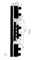
- FIG. 1Aillustrates a cross-sectional view of a conventional die-down ball grid array (BGA) package 100 .
- BGA package 100includes an IC die 105 , a die attach adhesive 125 , a heat spreader 110 , and a package substrate 120 .
- BGA package 100further includes a plurality of wire bonds 115 , a plurality of solder balls 130 , and an encapsulating material 135 .
- IC die 105is mounted to heat spreader 110 in a die-down configuration with die attach adhesive 125 .
- a first surface of substrate 120is attached to heat spreader 110 .
- Wire bonds 115couple signals of IC die 105 to a second surface of substrate 120 .
- Solder balls 130are attached to the second surface of substrate 120 .
- Solder balls 130are reflowed to attach BGA package 100 to a PCB (not shown in FIG. 1A ).
- a thermal pathis present in BGA package 100 from the active surface of IC die 105 to the PCB through encapsulating material 135 .
- typical encapsulating materials 135lack thermal conductivity.
- an indirect thermal pathis present from the active surface of IC die 105 to the PCB through adhesive 125 , heat spreader 110 , substrate 120 , and solder balls 130 .
- BGA package 100provides limited thermal performance because there is no direct thermally conductive path from the active surface of IC die 105 to the PCB.
- BGA package 100also provides limited electrical performance. For example, routing signals from the center of IC die 105 to substrate 120 with wire bonds 115 introduces increased resistance because wire bonds 115 increase in length with distance from the edge of IC die 105 . The increased resistance introduced by the longer electrical paths results in an undesirable drop in signal potential.
- FIG. 1Billustrates a cross-sectional view of a conventional die-up BGA package 150 .
- BGA package 150includes an IC die 155 , a package substrate 160 , a plurality of electrically conductive bumps 170 , a plurality of solder balls 175 , and an underfill material 165 .
- IC die 155is mounted to a first surface of substrate 160 in a die-up configuration. Electrically conductive bumps 170 of an active surface of IC die 155 are coupled to conductive pads on the first surface of substrate 160 . Electrically conductive bumps 170 couple signals in IC die 155 to substrate 160 .
- Underfill material 165is applied between the active surface of IC die 155 and the first surface of substrate 160 .
- Solder balls 175are attached to a second surface of substrate 160 . Solder balls 175 are reflowed to attach BGA package 150 to a PCB (not shown in FIG. 1B ).
- BGA package 150provides limited I/O performance because a high-density substrate 160 with numerous routing layers would be needed to effectively route a large number of signals from the array of conductive pads on the first surface of substrate 160 , to which IC die 155 is mounted. Numerous routing layers are undesirable because the cost of substrate 160 typically increases with the number of routing layers. In some cases (e.g., when the flip-chip bump pitch is extremely dense), it is not be possible with current technology to manufacture a substrate 160 having a high enough density.
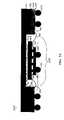
- FIG. 2Aillustrates a cross-sectional view of a die-down BGA package 200 , in accordance with an embodiment of the present invention.
- BGA package 200includes an IC die 205 , a die attach material 215 , a heat spreader 210 with a central cavity 255 formed therein, a package substrate 220 , and an interposer 240 .
- BGA package 200further includes an encapsulating material 260 , a plurality of wire bonds 230 , a plurality of corresponding bond pads 225 , a plurality of electrically conductive bumps 235 , a plurality of solder balls 245 , and a plurality of solder balls 250 .
- a first surface 211 of heat spreader 210has central cavity 255 formed therein.
- Substrate 220has a central opening 223 that is open at a first surface 221 and a second surface 222 of substrate 220 .
- First surface 221 of substrate 220is coupled to first surface 211 of heat spreader 210 .
- Central opening 223 through substrate 220overlaps central cavity 255 formed in heat spreader 210 .
- IC die 205is mounted in a die-down configuration with die attach adhesive 215 to first surface 211 in cavity 255 of heat spreader 210 .
- Solder balls 245are coupled to second surface 222 of substrate 220 .
- Bond pads 225are located on a peripheral area of an active surface 202 of IC die 205 .
- Wire bonds 230connect bond pads 225 to second surface 222 of substrate 220 (e.g., to traces, contacts, ground rings, ground planes, voltage planes, etc. of substrate 220 ).
- Bond pads 225can be any type of signal pads of IC die 205 , including I/O pads, voltage pads, ground pads, test pads, etc.
- Electrically conductive bumps 235are located on a central area of active surface 202 of IC die 205 , and are arranged in any configuration, including an array (i.e., in columns and rows). Electrically conductive bumps 235 are flip-chip coupled to corresponding bond pads (not shown in FIG. 2A ) on a first surface 241 of interposer 240 . Solder balls 250 are coupled to a second surface 242 of interposer 240 .
- FIGS. 2B and 2Cillustrate example bond pad 236 and solder ball 250 configurations on first and second surfaces 241 and 242 of interposer 240 , respectively, for BGA package 200 shown in FIG. 2A , according to an example embodiment of the present invention. It is noted that any number of bond pads 236 and solder balls 250 may be present in interposer 240 , as is desired for the particular implementation.
- Solder balls 245 and 250are reflowed to attach BGA package 200 to a PCB.
- Solder balls 245 and 250can be implemented with other types of electrically conductive terminals (e.g., pins, studs, other kinds of balls, etc.).
- An encapsulating material 260encapsulates IC die 205 and wire bonds 230 .
- an underfill material 265fills a space between active surface 202 of IC die 205 and first surface 241 of interposer 240 .
- Underfill material 265is typically applied before encapsulating material 260 , but can also be applied after encapsulating material 260 is applied.
- Example materials for underfill material 265include conventional underfill materials, including silicon oxide, or any other kind of underfill material.
- Underfill material 265is typically different from encapsulating material 260 but, in some cases, underfill material 265 and encapsulating material 260 can be the same material.
- Example materials for heat spreader 210include copper, aluminum, aluminum based alloys, copper based alloys, ferromagnetic materials, laminated copper/iron, other metals and combinations of metals/alloys, other thermally and/or electrically conductive materials (e.g., ceramics, metallized plastics, etc.), and other materials described elsewhere herein. Machining, etching, stamping, and other techniques can be used to form central cavity 255 in first surface 211 of heat spreader 210 .
- Example materials for die attach adhesive 215include epoxy, such as a silver epoxy, solder, and other adhesive materials.
- Example materials for substrate 220include tape, laminate, ceramic, organic (e.g., BT, FR4, etc.), and other materials.
- Substrate 220can have one or more electrical routing layers, which can be constructed through lamination, build-up, or other processes.
- Substrate 220can further include single or multi-layer electrical conductive traces or planes.
- Example materials for electrically conductive bumps 235include lead/tin solder, gold, gold/tin, other metal or metal composites, electrically conductive epoxy, and other electrically conductive materials.
- Example materials for interposer 240include tape, metal, a substrate (e.g., laminate or ceramic), an IC, or any combination of these materials (e.g., tape with metal stiffener, tape with laminate or ceramic substrate, IC with metal slug, etc). Reflow process, thermal compression, thermal sonic bonding, and other methods can be used to attach interposer 240 .
- Interposer 240can be attached either before wafer dice or singulation (i.e., when IC die 205 is in wafer form) or after IC die 205 has been singulated, including when it is attached to heat spreader 210 .
- BGA package 200includes both wire bond 230 and flip-chip 235 interconnections in the same package. Accordingly, BGA package 200 significantly increases the number of I/O signals that can be routed to and from IC die 205 , without reducing the minimum pitch of I/O pads on IC die 205 or requiring substrate 220 be high-density. Additionally, BGA package 200 has enhanced thermal properties due to the more direct thermal path from active surface 202 of IC die 205 to the PCB, through interposer 240 . BGA package 200 also has enhanced electrical properties due to the more direct electrical path from IC die 205 to the PCB, through interposer 240 .
- FIG. 3illustrates a cross-sectional view of a die-down BGA package 300 , in accordance with an embodiment of the present invention.
- BGA package 300is similar to BGA package 200 , shown in FIG. 2A , except a heat slug 305 replaces solder balls 250 for additional thermal enhancement.
- Heat slug 305has a first surface 306 coupled to second surface 242 of interposer 240 .
- Heat slug 305has a second surface 307 , which is configured to be surface mounted to a PCB.
- Example materials for heat slug 305include copper, aluminum, other metals or combinations of metals/alloys, ceramics, and other thermally and/or electrically conductive materials.
- heat slug 305is formed separately and then attached to interposer 240 .
- heat slug 305is formed by depositing a plating layer on second surface 242 of interposer 240 . Heat slug 305 can also be formed in other ways.
- BGA package 300is configured without a separate heat slug 305 .
- interposer 240incorporates the function of heat slug 305 , and second surface 242 of interposer 240 is configured to be mounted to the PCB.
- BGA package 300a single electrical signal can be routed from IC die 205 to the PCB through heat slug 305 . Accordingly, BGA package 300 is advantageous for routing a single power, ground, or other signal of IC die 205 to the PCB, through interposer 240 and heat slug 305 .
- BGA package 200shown in FIG. 2A , is advantageous for routing multiple I/O signals from IC die 205 , through the center of the package, to the PCB. Because BGA package 200 has solder balls 250 instead of heat slug 305 (shown in FIG. 3 ), multiple I/O signals can be routed from IC die 205 to the PCB, through interposer 240 and solder balls 250 . Accordingly, BGA package 200 provides a direct electrical path for routing critical I/O signals with less resistance and therefore little drop in signal potential.
- FIG. 4illustrates a cross-sectional view of a die-down BGA package 400 .
- BGA package 400is similar to BGA package 200 , shown in FIG. 2A , except that package 400 includes a two-piece heat spreader formed from a planar heat spreader 410 and a ring-shaped body 420 .
- BGA package 400includes IC die 205 , planar heat spreader 410 , adhesive material 215 , ring-shaped body 420 , substrate 220 , and interposer 240 .
- BGA package 400further includes plurality of wire bonds 230 , plurality of corresponding bond pads 225 , plurality of electrically conductive bumps 235 , plurality of solder balls 245 , and plurality of solder balls 250 .
- Elements in FIG. 4are generally similar to the corresponding elements shown in FIG. 2 , with differences described below.
- BGA package 400includes a two-piece heat spreader formed by coupling ring-shaped body 420 to planar heat spreader 410 .
- Ring-shaped body 420has a central opening that is open at a first surface 421 and a second surface 422 of ring-shaped body 420 .
- central cavity 255is formed in first surface 211 of heat spreader 210 .
- central cavity 255is formed by coupling first surface 421 of ring-shaped body 420 to a first surface 411 of planar heat spreader 410 with adhesive material 215 .
- First surface 221 of substrate 220is coupled to second surface 422 of ring-shaped body 420 .
- IC die 205is mounted with adhesive material 215 in a die-down configuration to first surface 411 of heat spreader 410 , within central cavity 255 .
- Solder balls 245are coupled to second surface 222 of substrate 220 .
- Example materials for heat spreader 410 and ring-shaped body 420include copper, aluminum, aluminum based alloys, copper based alloys, ferromagnetic materials, laminated copper/iron, other metals and combinations of metals/alloys, other thermally and/or electrically conductive materials (e.g., ceramics, metallized plastics, etc.), and other materials described elsewhere herein.
- Heat spreader 410 and ring-shaped body 420are typically made from the same material (e.g., to match coefficients of thermal expansion (CTE)), but can be made from different materials.
- CTEcoefficients of thermal expansion
- BGA package 400like BGA package 200 , described above, includes both wire bond 230 and flip-chip 235 interconnections in the same package. Therefore, BGA package 400 significantly increases the number of I/O signals that can be routed to and from IC die 205 , without reducing the minimum pitch of I/O pads on IC die 205 or requiring substrate 220 be high-density. Additionally, BGA package 400 has enhanced thermal properties due to the more direct thermal path from active surface 202 of IC die 205 to the PCB, through interposer 240 . BGA package 400 also has enhanced electrical properties due to the more direct electrical path from IC die 205 to the PCB, through interposer 240 .
- FIG. 5illustrates a cross-sectional view of a die-down BGA package 500 .
- BGA package 500is similar to BGA package 400 of FIG. 4 , except heat slug 305 replaces solder balls 250 for additional thermal enhancement, similarly to BGA package 300 shown in FIG. 3 .
- First surface 306 of heat slug 305is coupled to second surface 242 of interposer 240 .
- Second surface 307 of heat slug 305is configured to be mounted to a PCB.
- FIG. 6shows flowchart 600 , providing steps for assembling an array IC device package with enhanced thermal, electrical, and/or I/O properties, according to one or more embodiments of the present invention.
- FIGS. 7-9 , 10 A, and 10 Bprovide additional optional steps, according to further embodiments of the present invention.
- the steps of FIGS. 6-9 , 10 A, and 10 Bdo not necessarily have to occur in the order shown, as will be apparent to persons skilled in the relevant art(s) based on the teachings herein.
- Other operational and structural embodimentswill be apparent to persons skilled in the relevant art(s) based on the following discussion. These steps are described in detail below.
- Flowchart 600is shown in FIG. 6 , and begins with step 605 .
- a substrateis coupled to a heat spreader.
- the substrateis substrate 220
- the heat spreaderis heat spreader 210 , as shown in FIGS. 2A and 3 .
- an IC dieis mounted to the heat spreader.
- the IC dieis mounted in a central cavity formed in the heat spreader, and the IC die is IC die 205 , the heat spreader is heat spreader 210 , the central cavity is central cavity 255 , and the substrate is substrate 220 .
- a plurality of bond pads on the IC dieare coupled to corresponding bond pads on the substrate with wire bonds.
- the IC dieis IC die 205
- the plurality of bond pads on the IC dieis plurality of bond pads 225
- the substrateis substrate 220
- the wire bondsare wire bonds 230 , as shown in FIGS. 2 A and 3 - 5 .
- an interposeris coupled to the IC die so that a plurality of electrically conductive bumps on the IC die are coupled to corresponding bond pads on the interposer.
- the IC dieis IC die 205
- the plurality of electrically conductive bumps on the IC dieis plurality of electrically conductive bumps 235
- the interposeris interposer 240 , as shown in FIGS. 2 A and 3 - 5 .
- flowchart 600includes the step shown in FIG. 7 for forming a two-piece heat spreader.
- a ring-shaped bodyis coupled to a substantially planar heat spreader to form the heat spreader described in steps 605 and 610 of FIG. 6 .
- the ring-shaped bodyis ring-shaped body 420
- the planar heat spreaderis planar heat spreader 410 , as shown in FIGS. 4 and 5 .
- flowchart 600includes one or more of the steps shown in FIG. 8 .
- step 805an array of electrically conductive terminals is formed on the substrate.
- the array of electrically conductive terminals formed on the substrateis plurality of solder balls 245 , as shown in FIGS. 2A and 4 .
- an array of electrically conductive terminalsis formed on the interposer.
- the array of electrically conductive terminals formed on the interposeris plurality of solder balls 250 , as shown in FIGS. 2A and 4 .
- the arrays of electrically conductive terminals formed on the substrate in step 805 and on the interposer in step 810are configured to mount the package to a PCB.
- flowchart 600includes one or more of the steps shown in FIG. 9 .
- step 905an array of electrically conductive terminals is formed on the substrate.
- the array of electrically conductive terminals on the substrateis plurality of solder balls 245 , as shown in FIGS. 3 and 5 .
- the terminalscan be pins, pads, or other terminal type.
- a heat slugis coupled to the interposer.
- the heat slugis heat slug 305
- the interposeris interposer 240 , as shown in FIGS. 3 and 5 .
- the array of electrically conductive terminals on the substrate and a surface of the heat slugare configured to mount the package to a PCB.
- flowchart 600includes the step shown in FIG. 10A .
- step 1005a space between the active surface of the IC die and the interposer is filled in with an underfill material.
- the IC dieis IC die 205
- the active surface of the IC dieis active surface 202
- the interposeris interposer 240
- the underfill materialis underfill material 265 , as shown in FIG. 2D .
- flowchart 600includes the step shown in FIG. 10B .
- the IC die and the wire bondsare encapsulated with an encapsulating material.
- the IC dieis IC die 205
- the wire bondsare wire bonds 230
- the encapsulating materialis encapsulating material 260 , as shown in FIGS. 2A , 2 D, and 3 - 5 .
Landscapes
- Engineering & Computer Science (AREA)
- Microelectronics & Electronic Packaging (AREA)
- Physics & Mathematics (AREA)
- Condensed Matter Physics & Semiconductors (AREA)
- General Physics & Mathematics (AREA)
- Computer Hardware Design (AREA)
- Power Engineering (AREA)
- Chemical & Material Sciences (AREA)
- Materials Engineering (AREA)
- Cooling Or The Like Of Semiconductors Or Solid State Devices (AREA)
Abstract
Description
- This is a divisional application of pending U.S. application Ser. No. 10/870,928, filed Jun. 21, 2004 (Atty. Dkt. No. 1875.5840000), now allowed, which is herein incorporated by reference in its entirety.
- 1. Field of the Invention
- The invention relates generally to the field of integrated circuit (IC) device packaging technology and, more particularly to IC device packages with enhanced thermal, electrical, and input/output (I/O) properties.
- 2. Related Art
- IC semiconductor dies are typically mounted in or on a package that is attached to a printed circuit board (PCB). An array IC device package includes a plurality of electrically conductive terminals (e.g., solder balls, pins, pads, etc.) arranged in an array (i.e., columns and rows) on a bottom surface of a package substrate. Signals from an IC die mounted on a surface of the substrate are routed through the substrate to the electrically conductive terminals on the bottom surface. The electrically conductive terminals are configured to be attached to the PCB. Example array IC device packages include ball grid array (BGA), pin grid array (PGA), and land grid array (LGA) packages.
- Array IC device packages can have die-up and die-down configurations. In die-up packages, the IC die is mounted on a top surface of the substrate, opposite the surface to which the electrically conductive terminals are attached. In die-down packages, the IC die is mounted on the bottom surface of the substrate, on the same surface where the electrically conductive terminals are located.
- The present invention is directed to integrated circuit (IC) device packages that provide enhanced thermal, electrical, and input/output (I/O) performance, and methods for making the same.
- IC device packages are described herein having an IC die coupled to a substrate with at least one wire bond, and an interposer coupled to the IC die in a flip-chip fashion. Example embodiments of the present invention are described below.
- In an embodiment of the present invention, a die-down array IC device package includes a heat spreader having a first surface with a central cavity formed therein. The package further includes a substrate having a first surface coupled to the first surface of the heat spreader. An array of electrically conductive terminals is coupled to a second surface of the substrate. A central opening through the substrate overlaps the central cavity. The package further includes an IC die, which has a first surface mounted to the first surface of the heat spreader, within the central cavity. At least one wire bond couples at least one bond pad on a second surface of the IC die to at least one bond pad on the second surface of the substrate. The package further includes an interposer. A plurality of electrically conductive bumps on the second surface of the IC die is coupled to corresponding bond pads on a first surface of the interposer.
- In another embodiment of the present invention, the die-down array IC device package includes an underfill material that fills a space between the IC die and the interposer, and an encapsulating material that encapsulates the IC die and the at least one wire bond.
- In another embodiment of the present invention, the die-down array IC device package includes a heat slug coupled to a second surface of the interposer.
- In another embodiment of the present invention, the heat spreader includes a substantially planar body having opposing first and second surfaces, and a ring-shaped body having a central opening that is open at first and second surfaces of the ring-shaped body. The first surface of the ring-shaped body is coupled to the first surface of the substantially planar body. The second surfaces of the ring-shaped body and the substantially planar body form the first and second surfaces, respectively, of the heat spreader. The central opening through the ring-shaped body and a portion of the first surface of the substantially planar body that is exposed through the central opening form the central cavity.
- In another embodiment of the present invention, a method of making a die-down array IC device package includes the step of coupling a first surface of a substrate to a first surface of a heat spreader. The method further includes the step of mounting a first surface of an IC die to the first surface of the heat spreader, within a central cavity formed in the first surface of the heat spreader. The method further includes the step of coupling a plurality of bond pads on a second surface of the IC die to corresponding bond pads on a second surface of the substrate with a plurality of wire bonds. The method further includes the step of coupling a first surface of an interposer to the second surface of the IC die so that a plurality of electrically conductive bumps on the second surface of the IC die is coupled to corresponding bond pads on the first surface of the interposer.
- In another embodiment of the present invention, the method further includes the steps of filling a space between the IC die and the interposer with an underfill material, and encapsulating the IC die and the plurality of wire bonds with an encapsulating material.
- In another embodiment of the present invention, the method further includes the step of coupling a heat slug to a second surface the interposer.
- In another embodiment of the present invention, the method includes the step of coupling a first surface of a ring-shaped body to a first surface of a substantially planar body to form the heat spreader. Second surfaces of the ring-shaped body and the substantially planar body form the first and second surfaces of said heat spreader, respectively. The central opening through the substrate overlaps a central opening through the ring-shaped body that is open at the first and second surfaces of the ring-shaped body.
- Further embodiments, features, and advantages of the present invention, as well as the structure and operation of various example embodiments of the present invention, are described in detail below with reference to the accompanying drawings.
- The accompanying drawings, which are incorporated herein and form a part of the specification, illustrate the present invention and, together with the description, further serve to explain the principles of the invention and to enable a person skilled in the pertinent art to make and use the invention. The drawing in which an element first appears is typically indicated by the leftmost digit(s) in the corresponding reference number.
FIG. 1A illustrates a cross-sectional view of a conventional die-down BGA package with wire bond interconnections.FIG. 1B illustrates a cross-sectional view of a conventional die-up BGA package with flip-chip interconnections.FIG. 2A illustrates a cross-sectional view of a die-down BGA package, having an interposer attached to a flip-chip mounted IC die, in accordance with an example embodiment of the present invention.FIGS. 2B and 2C illustrate top and bottom views, respectively, of the interposer illustrated inFIG. 2A , in accordance with an example embodiment of the present invention.FIG. 2D illustrates the die-down BGA package shown inFIG. 2A , having an underfill material between the interposer and the IC die, in accordance with an example embodiment of the present invention.FIG. 3 illustrates a cross-sectional view of a die-down BGA package, having an interposer attached to a flip-chip mounted IC die and a heat slug attached to the interposer, in accordance with an example embodiment of the present invention.FIG. 4 illustrates a cross-sectional view of a die-down BGA package, having a two-piece heat spreader, and an interposer attached to a flip-chip mounted IC die, in accordance with an example embodiment of the present invention.FIG. 5 illustrates a cross-sectional view of a die-down BGA package, having a two-piece heat spreader, an interposer attached to a flip-chip mounted IC die, and a heat slug attached to the interposer, in accordance with an example embodiment of the present invention.FIGS. 6-9 ,10A, and10B show flowcharts providing example steps for assembling die-down array IC device packages with enhanced thermal, electrical, and/or input/output (I/O) performance, in accordance with example embodiments of the present invention.- Some conventional array integrated circuit (IC) device packages have wire bond interconnections to couple signals of the IC die from corresponding bond pads on the active surface of the IC die to the package substrate. Other conventional array IC device packages have flip-chip interconnections to couple signals of the IC die from an array of conductive bumps on the active surface of the IC die to the package substrate. The package substrate has internal routing that electrically couples the signals of the IC die to an array of electrically conductive terminals on a bottom surface of the substrate, and the package is typically mounted to a printed circuit board (PCB).
- Conventional array IC device packages having only wire bond interconnections to route signals from the IC die suffer from limited thermal and electrical performance. For example, thermal performance is limited because there is no direct thermal path from the active surface of the IC die to the PCB. Electrical performance is also limited because there is no direct electrical path for routing signals from the center of the IC die to the PCB. For example, signals routed from the center of the IC die traverse a longer electrical path than signals routed from an edge. Relatively short electrical paths are desirable because they introduce less resistance than relatively long electrical paths. Signals traversing relatively long electrical paths can experience significant drops in potential due to the increased resistance.
- Furthermore, conventional IC device packages having only wire bond interconnections or having only flip-chip interconnections to route signals from the IC die suffer from limited input/output (I/O) performance. In order to achieve more I/Os with wire bond interconnections, the minimum pitch of the I/O pads on the IC die must be reduced accordingly. In order to route more I/Os from the IC die to the PCB with flip-chip interconnections, more substrate layers are required. However, the cost of high-density substrates increases with the number of layers required and, in some cases (e.g., when the flip-chip bump pitch is extremely dense), it is not possible with current technology to manufacture a substrate having a high enough density.
- Therefore, what is needed are IC device packages that provide enhanced thermal, electrical, and I/O performance.
- The present invention is directed to IC device packages having enhanced thermal, electrical, and I/O properties, and methods of making the same. In embodiments, an active surface of the IC die has at least one bond pad for wire bond interconnections to a package substrate, in addition to at least one electrically conductive bump for flip-chip interconnection to an interposer. The substrate and the interposer are configured to be coupled to a PCB.
- In embodiments, enhanced thermal properties are present due to a direct thermal path from the active surface of the IC die to the PCB, through the interposer. In further embodiments, enhanced electrical properties are present due to a direct electrical path from the active surface of the IC die to the PCB, through the interposer. Additionally, because both wire bond pads and flip-chip bumps are used to interconnect signals, more I/O connections can be achieved compared to conventional IC device packages having either wire bond or flip-chip interconnections alone.
- While example embodiments of the present invention described below are illustrated with a die-down configuration, it is noted that they can alternatively be implemented with a die-up configuration.
- In the next section, conventional IC device packages are described. The subsequent section then describes example IC device package embodiments of the present invention, followed by a description of example embodiments for assembling IC device packages of the present invention. These embodiments are provided for illustrative purposes, and the present invention is not limited to these examples.
FIG. 1A illustrates a cross-sectional view of a conventional die-down ball grid array (BGA)package 100.BGA package 100 includes an IC die105, a die attach adhesive125, aheat spreader 110, and apackage substrate 120.BGA package 100 further includes a plurality of wire bonds115, a plurality of solder balls130, and an encapsulatingmaterial 135. IC die105 is mounted toheat spreader 110 in a die-down configuration with die attach adhesive125. A first surface ofsubstrate 120 is attached to heatspreader 110. Wire bonds115 couple signals of IC die105 to a second surface ofsubstrate 120. Solder balls130 are attached to the second surface ofsubstrate 120. Solder balls130 are reflowed to attachBGA package 100 to a PCB (not shown inFIG. 1A ).- A thermal path is present in
BGA package 100 from the active surface of IC die105 to the PCB through encapsulatingmaterial 135. However,typical encapsulating materials 135 lack thermal conductivity. Alternatively, an indirect thermal path is present from the active surface of IC die105 to the PCB through adhesive125,heat spreader 110,substrate 120, and solder balls130. Thus,BGA package 100 provides limited thermal performance because there is no direct thermally conductive path from the active surface of IC die105 to the PCB.BGA package 100 also provides limited electrical performance. For example, routing signals from the center of IC die105 tosubstrate 120 with wire bonds115 introduces increased resistance because wire bonds115 increase in length with distance from the edge of IC die105. The increased resistance introduced by the longer electrical paths results in an undesirable drop in signal potential. FIG. 1B illustrates a cross-sectional view of a conventional die-upBGA package 150.BGA package 150 includes anIC die 155, apackage substrate 160, a plurality of electricallyconductive bumps 170, a plurality ofsolder balls 175, and anunderfill material 165. IC die155 is mounted to a first surface ofsubstrate 160 in a die-up configuration. Electricallyconductive bumps 170 of an active surface of IC die155 are coupled to conductive pads on the first surface ofsubstrate 160. Electricallyconductive bumps 170 couple signals in IC die155 tosubstrate 160.Underfill material 165 is applied between the active surface of IC die155 and the first surface ofsubstrate 160.Solder balls 175 are attached to a second surface ofsubstrate 160.Solder balls 175 are reflowed to attachBGA package 150 to a PCB (not shown inFIG. 1B ).BGA package 150 provides limited I/O performance because a high-density substrate 160 with numerous routing layers would be needed to effectively route a large number of signals from the array of conductive pads on the first surface ofsubstrate 160, to which IC die155 is mounted. Numerous routing layers are undesirable because the cost ofsubstrate 160 typically increases with the number of routing layers. In some cases (e.g., when the flip-chip bump pitch is extremely dense), it is not be possible with current technology to manufacture asubstrate 160 having a high enough density.FIG. 2A illustrates a cross-sectional view of a die-down BGA package 200, in accordance with an embodiment of the present invention.BGA package 200 includes anIC die 205, a die attachmaterial 215, aheat spreader 210 with acentral cavity 255 formed therein, apackage substrate 220, and aninterposer 240.BGA package 200 further includes an encapsulatingmaterial 260, a plurality ofwire bonds 230, a plurality ofcorresponding bond pads 225, a plurality of electricallyconductive bumps 235, a plurality ofsolder balls 245, and a plurality ofsolder balls 250.- A
first surface 211 ofheat spreader 210 hascentral cavity 255 formed therein.Substrate 220 has acentral opening 223 that is open at afirst surface 221 and asecond surface 222 ofsubstrate 220.First surface 221 ofsubstrate 220 is coupled tofirst surface 211 ofheat spreader 210.Central opening 223 throughsubstrate 220 overlapscentral cavity 255 formed inheat spreader 210. IC die205 is mounted in a die-down configuration with die attach adhesive215 tofirst surface 211 incavity 255 ofheat spreader 210.Solder balls 245 are coupled tosecond surface 222 ofsubstrate 220. Bond pads 225 are located on a peripheral area of anactive surface 202 of IC die205.Wire bonds 230connect bond pads 225 tosecond surface 222 of substrate220 (e.g., to traces, contacts, ground rings, ground planes, voltage planes, etc. of substrate220).Bond pads 225 can be any type of signal pads of IC die205, including I/O pads, voltage pads, ground pads, test pads, etc.- Electrically
conductive bumps 235 are located on a central area ofactive surface 202 of IC die205, and are arranged in any configuration, including an array (i.e., in columns and rows). Electricallyconductive bumps 235 are flip-chip coupled to corresponding bond pads (not shown inFIG. 2A ) on afirst surface 241 ofinterposer 240.Solder balls 250 are coupled to asecond surface 242 ofinterposer 240.FIGS. 2B and 2C illustrateexample bond pad 236 andsolder ball 250 configurations on first andsecond surfaces interposer 240, respectively, forBGA package 200 shown inFIG. 2A , according to an example embodiment of the present invention. It is noted that any number ofbond pads 236 andsolder balls 250 may be present ininterposer 240, as is desired for the particular implementation. Solder balls BGA package 200 to a PCB.Solder balls - An encapsulating
material 260 encapsulates IC die205 andwire bonds 230. In another embodiment, shown inFIG. 2D , anunderfill material 265 fills a space betweenactive surface 202 of IC die205 andfirst surface 241 ofinterposer 240.Underfill material 265 is typically applied before encapsulatingmaterial 260, but can also be applied after encapsulatingmaterial 260 is applied. Example materials forunderfill material 265 include conventional underfill materials, including silicon oxide, or any other kind of underfill material.Underfill material 265 is typically different from encapsulatingmaterial 260 but, in some cases,underfill material 265 and encapsulatingmaterial 260 can be the same material. - Example materials for
heat spreader 210 include copper, aluminum, aluminum based alloys, copper based alloys, ferromagnetic materials, laminated copper/iron, other metals and combinations of metals/alloys, other thermally and/or electrically conductive materials (e.g., ceramics, metallized plastics, etc.), and other materials described elsewhere herein. Machining, etching, stamping, and other techniques can be used to formcentral cavity 255 infirst surface 211 ofheat spreader 210. Example materials for die attach adhesive215 include epoxy, such as a silver epoxy, solder, and other adhesive materials. - Example materials for
substrate 220 include tape, laminate, ceramic, organic (e.g., BT, FR4, etc.), and other materials.Substrate 220 can have one or more electrical routing layers, which can be constructed through lamination, build-up, or other processes.Substrate 220 can further include single or multi-layer electrical conductive traces or planes. - Example materials for electrically
conductive bumps 235 include lead/tin solder, gold, gold/tin, other metal or metal composites, electrically conductive epoxy, and other electrically conductive materials. - Example materials for
interposer 240 include tape, metal, a substrate (e.g., laminate or ceramic), an IC, or any combination of these materials (e.g., tape with metal stiffener, tape with laminate or ceramic substrate, IC with metal slug, etc). Reflow process, thermal compression, thermal sonic bonding, and other methods can be used to attachinterposer 240.Interposer 240 can be attached either before wafer dice or singulation (i.e., when IC die205 is in wafer form) or after IC die205 has been singulated, including when it is attached to heatspreader 210. - Advantageously,
BGA package 200 includes bothwire bond 230 and flip-chip 235 interconnections in the same package. Accordingly,BGA package 200 significantly increases the number of I/O signals that can be routed to and from IC die205, without reducing the minimum pitch of I/O pads on IC die205 or requiringsubstrate 220 be high-density. Additionally,BGA package 200 has enhanced thermal properties due to the more direct thermal path fromactive surface 202 of IC die205 to the PCB, throughinterposer 240.BGA package 200 also has enhanced electrical properties due to the more direct electrical path from IC die205 to the PCB, throughinterposer 240. FIG. 3 illustrates a cross-sectional view of a die-down BGA package 300, in accordance with an embodiment of the present invention.BGA package 300 is similar toBGA package 200, shown inFIG. 2A , except aheat slug 305 replacessolder balls 250 for additional thermal enhancement.Heat slug 305 has afirst surface 306 coupled tosecond surface 242 ofinterposer 240.Heat slug 305 has asecond surface 307, which is configured to be surface mounted to a PCB.- Example materials for
heat slug 305 include copper, aluminum, other metals or combinations of metals/alloys, ceramics, and other thermally and/or electrically conductive materials. In an example embodiment,heat slug 305 is formed separately and then attached tointerposer 240. In another embodiment,heat slug 305 is formed by depositing a plating layer onsecond surface 242 ofinterposer 240.Heat slug 305 can also be formed in other ways. - Alternatively, in another embodiment,
BGA package 300 is configured without aseparate heat slug 305. Instead,interposer 240 incorporates the function ofheat slug 305, andsecond surface 242 ofinterposer 240 is configured to be mounted to the PCB. - In
BGA package 300, a single electrical signal can be routed from IC die205 to the PCB throughheat slug 305. Accordingly,BGA package 300 is advantageous for routing a single power, ground, or other signal of IC die205 to the PCB, throughinterposer 240 andheat slug 305. - In comparison,
BGA package 200, shown inFIG. 2A , is advantageous for routing multiple I/O signals from IC die205, through the center of the package, to the PCB. BecauseBGA package 200 hassolder balls 250 instead of heat slug305 (shown inFIG. 3 ), multiple I/O signals can be routed from IC die205 to the PCB, throughinterposer 240 andsolder balls 250. Accordingly,BGA package 200 provides a direct electrical path for routing critical I/O signals with less resistance and therefore little drop in signal potential. FIG. 4 illustrates a cross-sectional view of a die-down BGA package 400.BGA package 400 is similar toBGA package 200, shown inFIG. 2A , except thatpackage 400 includes a two-piece heat spreader formed from aplanar heat spreader 410 and a ring-shapedbody 420.BGA package 400 includes IC die205,planar heat spreader 410,adhesive material 215, ring-shapedbody 420,substrate 220, andinterposer 240.BGA package 400 further includes plurality ofwire bonds 230, plurality ofcorresponding bond pads 225, plurality of electricallyconductive bumps 235, plurality ofsolder balls 245, and plurality ofsolder balls 250. Elements inFIG. 4 are generally similar to the corresponding elements shown inFIG. 2 , with differences described below.BGA package 400 includes a two-piece heat spreader formed by coupling ring-shapedbody 420 toplanar heat spreader 410. Ring-shapedbody 420 has a central opening that is open at afirst surface 421 and asecond surface 422 of ring-shapedbody 420. InBGA package 200 shown inFIG. 2A ,central cavity 255 is formed infirst surface 211 ofheat spreader 210. InBGA package 400 shown inFIG. 4 ,central cavity 255 is formed by couplingfirst surface 421 of ring-shapedbody 420 to afirst surface 411 ofplanar heat spreader 410 withadhesive material 215.First surface 221 ofsubstrate 220 is coupled tosecond surface 422 of ring-shapedbody 420.Central opening 223 throughsubstrate 220 overlapscentral cavity 255. IC die205 is mounted withadhesive material 215 in a die-down configuration tofirst surface 411 ofheat spreader 410, withincentral cavity 255.Solder balls 245 are coupled tosecond surface 222 ofsubstrate 220.- Example materials for
heat spreader 410 and ring-shapedbody 420 include copper, aluminum, aluminum based alloys, copper based alloys, ferromagnetic materials, laminated copper/iron, other metals and combinations of metals/alloys, other thermally and/or electrically conductive materials (e.g., ceramics, metallized plastics, etc.), and other materials described elsewhere herein.Heat spreader 410 and ring-shapedbody 420 are typically made from the same material (e.g., to match coefficients of thermal expansion (CTE)), but can be made from different materials. - Advantageously,
BGA package 400, likeBGA package 200, described above, includes bothwire bond 230 and flip-chip 235 interconnections in the same package. Therefore,BGA package 400 significantly increases the number of I/O signals that can be routed to and from IC die205, without reducing the minimum pitch of I/O pads on IC die205 or requiringsubstrate 220 be high-density. Additionally,BGA package 400 has enhanced thermal properties due to the more direct thermal path fromactive surface 202 of IC die205 to the PCB, throughinterposer 240.BGA package 400 also has enhanced electrical properties due to the more direct electrical path from IC die205 to the PCB, throughinterposer 240. FIG. 5 illustrates a cross-sectional view of a die-down BGA package 500.BGA package 500 is similar toBGA package 400 ofFIG. 4 , exceptheat slug 305 replacessolder balls 250 for additional thermal enhancement, similarly toBGA package 300 shown inFIG. 3 .First surface 306 ofheat slug 305 is coupled tosecond surface 242 ofinterposer 240.Second surface 307 ofheat slug 305 is configured to be mounted to a PCB.- Alternatively, in another embodiment,
BGA package 500 is configured without aseparate heat slug 305. Instead,interposer 240 incorporates the function ofheat slug 305, andsecond surface 242 ofinterposer 240 is configured to be mounted to the PCB. - Method of Assembling a Thermal, Electrical, and/or I/O Enhanced Package
FIG. 6 shows flowchart600, providing steps for assembling an array IC device package with enhanced thermal, electrical, and/or I/O properties, according to one or more embodiments of the present invention.FIGS. 7-9 ,10A, and10B provide additional optional steps, according to further embodiments of the present invention. The steps ofFIGS. 6-9 ,10A, and10B do not necessarily have to occur in the order shown, as will be apparent to persons skilled in the relevant art(s) based on the teachings herein. Other operational and structural embodiments will be apparent to persons skilled in the relevant art(s) based on the following discussion. These steps are described in detail below.- Flowchart600 is shown in
FIG. 6 , and begins withstep 605. Instep 605, a substrate is coupled to a heat spreader. For example, the substrate issubstrate 220, and the heat spreader isheat spreader 210, as shown inFIGS. 2A and 3 . - In
step 610, an IC die is mounted to the heat spreader. For example, as shown inFIGS. 2A and 3 , the IC die is mounted in a central cavity formed in the heat spreader, and the IC die isIC die 205, the heat spreader isheat spreader 210, the central cavity iscentral cavity 255, and the substrate issubstrate 220. - In step615, a plurality of bond pads on the IC die are coupled to corresponding bond pads on the substrate with wire bonds. For example, the IC die is
IC die 205, the plurality of bond pads on the IC die is plurality ofbond pads 225, the substrate issubstrate 220, and the wire bonds arewire bonds 230, as shown in FIGS.2A and3-5. - In
step 620, an interposer is coupled to the IC die so that a plurality of electrically conductive bumps on the IC die are coupled to corresponding bond pads on the interposer. For example, the IC die isIC die 205, the plurality of electrically conductive bumps on the IC die is plurality of electricallyconductive bumps 235, and the interposer isinterposer 240, as shown in FIGS.2A and3-5. - Alternatively, in another embodiment, flowchart600 includes the step shown in
FIG. 7 for forming a two-piece heat spreader. Instep 705, a ring-shaped body is coupled to a substantially planar heat spreader to form the heat spreader described insteps FIG. 6 . For example, the ring-shaped body is ring-shapedbody 420, and the planar heat spreader isplanar heat spreader 410, as shown inFIGS. 4 and 5 . - In another example embodiment, flowchart600 includes one or more of the steps shown in
FIG. 8 . Instep 805, an array of electrically conductive terminals is formed on the substrate. For example, the array of electrically conductive terminals formed on the substrate is plurality ofsolder balls 245, as shown inFIGS. 2A and 4 . - In step810, an array of electrically conductive terminals is formed on the interposer. For example, the array of electrically conductive terminals formed on the interposer is plurality of
solder balls 250, as shown inFIGS. 2A and 4 . The arrays of electrically conductive terminals formed on the substrate instep 805 and on the interposer in step810 are configured to mount the package to a PCB. - In an alternate example embodiment, flowchart600 includes one or more of the steps shown in
FIG. 9 . In step905, an array of electrically conductive terminals is formed on the substrate. For example, the array of electrically conductive terminals on the substrate is plurality ofsolder balls 245, as shown inFIGS. 3 and 5 . Alternatively, the terminals can be pins, pads, or other terminal type. - In
step 910, a heat slug is coupled to the interposer. For example, the heat slug isheat slug 305, and the interposer isinterposer 240, as shown inFIGS. 3 and 5 . The array of electrically conductive terminals on the substrate and a surface of the heat slug are configured to mount the package to a PCB. - In another example embodiment, flowchart600 includes the step shown in
FIG. 10A . Instep 1005, a space between the active surface of the IC die and the interposer is filled in with an underfill material. For example, the IC die isIC die 205, the active surface of the IC die isactive surface 202, the interposer isinterposer 240, and the underfill material is underfillmaterial 265, as shown inFIG. 2D . - In another example embodiment, flowchart600 includes the step shown in
FIG. 10B . In step1010, the IC die and the wire bonds are encapsulated with an encapsulating material. For example, the IC die isIC die 205, the wire bonds arewire bonds 230, and the encapsulating material is encapsulatingmaterial 260, as shown inFIGS. 2A ,2D, and3-5. - While various embodiments of the present invention have been described above, it should be understood that they have been presented by way of example only, and not limitation. It will be apparent to persons skilled in the relevant art that various changes in form and detail can be made therein without departing from the spirit and scope of the invention. Thus, the breadth and scope of the present invention should not be limited by any of the above-described exemplary embodiments, but should be defined only in accordance with the following claims and their equivalents.
Claims (16)
Priority Applications (1)
| Application Number | Priority Date | Filing Date | Title |
|---|---|---|---|
| US12/058,067US7595227B2 (en) | 2004-06-21 | 2008-03-28 | Integrated circuit device package having both wire bond and flip-chip interconnections and method of making the same |
Applications Claiming Priority (2)
| Application Number | Priority Date | Filing Date | Title |
|---|---|---|---|
| US10/870,928US7411281B2 (en) | 2004-06-21 | 2004-06-21 | Integrated circuit device package having both wire bond and flip-chip interconnections and method of making the same |
| US12/058,067US7595227B2 (en) | 2004-06-21 | 2008-03-28 | Integrated circuit device package having both wire bond and flip-chip interconnections and method of making the same |
Related Parent Applications (1)
| Application Number | Title | Priority Date | Filing Date |
|---|---|---|---|
| US10/870,928DivisionUS7411281B2 (en) | 2004-06-21 | 2004-06-21 | Integrated circuit device package having both wire bond and flip-chip interconnections and method of making the same |
Publications (2)
| Publication Number | Publication Date |
|---|---|
| US20080182364A1true US20080182364A1 (en) | 2008-07-31 |
| US7595227B2 US7595227B2 (en) | 2009-09-29 |
Family
ID=35479792
Family Applications (2)
| Application Number | Title | Priority Date | Filing Date |
|---|---|---|---|
| US10/870,928Expired - Fee RelatedUS7411281B2 (en) | 2004-06-21 | 2004-06-21 | Integrated circuit device package having both wire bond and flip-chip interconnections and method of making the same |
| US12/058,067Expired - Fee RelatedUS7595227B2 (en) | 2004-06-21 | 2008-03-28 | Integrated circuit device package having both wire bond and flip-chip interconnections and method of making the same |
Family Applications Before (1)
| Application Number | Title | Priority Date | Filing Date |
|---|---|---|---|
| US10/870,928Expired - Fee RelatedUS7411281B2 (en) | 2004-06-21 | 2004-06-21 | Integrated circuit device package having both wire bond and flip-chip interconnections and method of making the same |
Country Status (1)
| Country | Link |
|---|---|
| US (2) | US7411281B2 (en) |
Cited By (9)
| Publication number | Priority date | Publication date | Assignee | Title |
|---|---|---|---|---|
| US20070040267A1 (en)* | 2005-08-22 | 2007-02-22 | Broadcom Corporation | Method and system for secure heat sink attachment on semiconductor devices with macroscopic uneven surface features |
| US20070120228A1 (en)* | 2004-03-29 | 2007-05-31 | Yamaha Corporation | Semiconductor wafer and manufacturing method therefor |
| US7714453B2 (en) | 2006-05-12 | 2010-05-11 | Broadcom Corporation | Interconnect structure and formation for package stacking of molded plastic area array package |
| US7786591B2 (en) | 2004-09-29 | 2010-08-31 | Broadcom Corporation | Die down ball grid array package |
| US20120056178A1 (en)* | 2010-09-06 | 2012-03-08 | Samsung Electronics Co., Ltd. | Multi-chip packages |
| US8581381B2 (en) | 2006-06-20 | 2013-11-12 | Broadcom Corporation | Integrated circuit (IC) package stacking and IC packages formed by same |
| US9515052B1 (en)* | 2015-06-26 | 2016-12-06 | SK Hynix Inc. | Semiconductor package including a step type substrate |
| US11209598B2 (en) | 2019-02-28 | 2021-12-28 | International Business Machines Corporation | Photonics package with face-to-face bonding |
| US20220283387A1 (en)* | 2021-03-03 | 2022-09-08 | Taiwan Semiconductor Manufacturing Co., Ltd. | Heterogeneous packaging integration of photonic and electronic elements |
Families Citing this family (42)
| Publication number | Priority date | Publication date | Assignee | Title |
|---|---|---|---|---|
| TWI234860B (en)* | 2004-04-02 | 2005-06-21 | Advanced Semiconductor Eng | Chip package and process thereof |
| US7271479B2 (en)* | 2004-11-03 | 2007-09-18 | Broadcom Corporation | Flip chip package including a non-planar heat spreader and method of making the same |
| KR100618892B1 (en)* | 2005-04-13 | 2006-09-01 | 삼성전자주식회사 | Semiconductor package achieves fan-out structure through wire bonding |
| KR100725517B1 (en)* | 2005-08-08 | 2007-06-07 | 삼성전자주식회사 | Multi-layer wiring board having bonding pads and ball lands formed in a plurality of layers and semiconductor package structure using the same |
| US7582951B2 (en) | 2005-10-20 | 2009-09-01 | Broadcom Corporation | Methods and apparatus for improved thermal performance and electromagnetic interference (EMI) shielding in leadframe integrated circuit (IC) packages |
| KR100885419B1 (en)* | 2006-04-26 | 2009-02-24 | 삼성전자주식회사 | Stacked Package Structure |
| US9299634B2 (en)* | 2006-05-16 | 2016-03-29 | Broadcom Corporation | Method and apparatus for cooling semiconductor device hot blocks and large scale integrated circuit (IC) using integrated interposer for IC packages |
| US8183680B2 (en) | 2006-05-16 | 2012-05-22 | Broadcom Corporation | No-lead IC packages having integrated heat spreader for electromagnetic interference (EMI) shielding and thermal enhancement |
| US20070273023A1 (en)* | 2006-05-26 | 2007-11-29 | Broadcom Corporation | Integrated circuit package having exposed thermally conducting body |
| US7808087B2 (en)* | 2006-06-01 | 2010-10-05 | Broadcom Corporation | Leadframe IC packages having top and bottom integrated heat spreaders |
| US9013035B2 (en)* | 2006-06-20 | 2015-04-21 | Broadcom Corporation | Thermal improvement for hotspots on dies in integrated circuit packages |
| US7906844B2 (en)* | 2006-09-26 | 2011-03-15 | Compass Technology Co. Ltd. | Multiple integrated circuit die package with thermal performance |
| US8169067B2 (en)* | 2006-10-20 | 2012-05-01 | Broadcom Corporation | Low profile ball grid array (BGA) package with exposed die and method of making same |
| US8183687B2 (en) | 2007-02-16 | 2012-05-22 | Broadcom Corporation | Interposer for die stacking in semiconductor packages and the method of making the same |
| US20080298024A1 (en)* | 2007-05-31 | 2008-12-04 | A.L.M.T. Corp. | Heat spreader and method for manufacturing the same, and semiconductor device |
| US7872335B2 (en)* | 2007-06-08 | 2011-01-18 | Broadcom Corporation | Lead frame-BGA package with enhanced thermal performance and I/O counts |
| US20090283889A1 (en)* | 2008-05-16 | 2009-11-19 | Byoung Wook Jang | Integrated circuit package system |
| RU2386190C1 (en)* | 2008-12-05 | 2010-04-10 | Закрытое акционерное общество "Научно-производственное объединение "НИИТАЛ" (ЗАО "НПО "НИИТАЛ") | Body of integrated circuit |
| US8633597B2 (en)* | 2010-03-01 | 2014-01-21 | Qualcomm Incorporated | Thermal vias in an integrated circuit package with an embedded die |
| US8718550B2 (en) | 2011-09-28 | 2014-05-06 | Broadcom Corporation | Interposer package structure for wireless communication element, thermal enhancement, and EMI shielding |
| US8780600B2 (en)* | 2011-12-07 | 2014-07-15 | Apple Inc. | Systems and methods for stacked semiconductor memory devices |
| US9209121B2 (en) | 2013-02-01 | 2015-12-08 | Analog Devices, Inc. | Double-sided package |
| CN105210185A (en)* | 2013-05-17 | 2015-12-30 | 富士通株式会社 | Semiconductor device, semiconductor device manufacturing method, and electronic apparatus |
| US9318411B2 (en)* | 2013-11-13 | 2016-04-19 | Brodge Semiconductor Corporation | Semiconductor package with package-on-package stacking capability and method of manufacturing the same |
| EP2947692B1 (en)* | 2013-12-20 | 2020-09-23 | Analog Devices, Inc. | Integrated device die and package with stress reduction features |
| US9638596B2 (en) | 2014-04-08 | 2017-05-02 | Freescale Semiconductor, Inc. | Cavity-down pressure sensor device |
| KR102228461B1 (en)* | 2014-04-30 | 2021-03-17 | 삼성전자주식회사 | Semiconductor Package Device |
| US20150340308A1 (en)* | 2014-05-21 | 2015-11-26 | Broadcom Corporation | Reconstituted interposer semiconductor package |
| US9401612B2 (en) | 2014-09-16 | 2016-07-26 | Navitas Semiconductor Inc. | Pulsed level shift and inverter circuits for GaN devices |
| US9731959B2 (en) | 2014-09-25 | 2017-08-15 | Analog Devices, Inc. | Integrated device packages having a MEMS die sealed in a cavity by a processor die and method of manufacturing the same |
| US9533878B2 (en) | 2014-12-11 | 2017-01-03 | Analog Devices, Inc. | Low stress compact device packages |
| US10287161B2 (en) | 2015-07-23 | 2019-05-14 | Analog Devices, Inc. | Stress isolation features for stacked dies |
| US9570372B1 (en)* | 2016-03-24 | 2017-02-14 | Bridge Semiconductor Corporation | Thermally enhanced semiconductor assembly with heat spreader and integrated dual build-up circuitries and method of making the same |
| US11112841B2 (en)* | 2017-04-01 | 2021-09-07 | Intel Corporation | 5G mmWave cooling through PCB |
| CN107369663A (en)* | 2017-08-25 | 2017-11-21 | 广东工业大学 | A kind of chip of fan-out package structure for possessing front salient point and preparation method thereof |
| US11127716B2 (en) | 2018-04-12 | 2021-09-21 | Analog Devices International Unlimited Company | Mounting structures for integrated device packages |
| US11296005B2 (en) | 2019-09-24 | 2022-04-05 | Analog Devices, Inc. | Integrated device package including thermally conductive element and method of manufacturing same |
| KR102778971B1 (en) | 2019-12-18 | 2025-03-11 | 삼성전자주식회사 | Printed circuit board and electronic device having the same |
| JP7290201B2 (en) | 2020-06-05 | 2023-06-13 | 日本電気株式会社 | quantum device |
| US11664340B2 (en) | 2020-07-13 | 2023-05-30 | Analog Devices, Inc. | Negative fillet for mounting an integrated device die to a carrier |
| US20230090133A1 (en)* | 2021-09-21 | 2023-03-23 | Bai Nie | Die first fan-out architecture for electric and optical integration |
| US12315776B2 (en) | 2021-11-08 | 2025-05-27 | Analog Devices, Inc. | Integrated device package with an integrated heat sink |
Citations (97)
| Publication number | Priority date | Publication date | Assignee | Title |
|---|---|---|---|---|
| US599415A (en)* | 1898-02-22 | Cromwell | ||
| US3790866A (en)* | 1973-05-14 | 1974-02-05 | Gen Motors Corp | Semiconductor device enclosure and method of making same |
| US5045921A (en)* | 1989-12-26 | 1991-09-03 | Motorola, Inc. | Pad array carrier IC device using flexible tape |
| US5208504A (en)* | 1990-12-28 | 1993-05-04 | Raytheon Company | Saw device and method of manufacture |
| US5216278A (en)* | 1990-12-04 | 1993-06-01 | Motorola, Inc. | Semiconductor device having a pad array carrier package |
| US5285352A (en)* | 1992-07-15 | 1994-02-08 | Motorola, Inc. | Pad array semiconductor device with thermal conductor and process for making the same |
| US5291062A (en)* | 1993-03-01 | 1994-03-01 | Motorola, Inc. | Area array semiconductor device having a lid with functional contacts |
| US5294826A (en)* | 1993-04-16 | 1994-03-15 | Northern Telecom Limited | Integrated circuit package and assembly thereof for thermal and EMI management |
| US5394009A (en)* | 1993-07-30 | 1995-02-28 | Sun Microsystems, Inc. | Tab semiconductor package with cushioned land grid array outer lead bumps |
| US5397917A (en)* | 1993-04-26 | 1995-03-14 | Motorola, Inc. | Semiconductor package capable of spreading heat |
| US5397921A (en)* | 1993-09-03 | 1995-03-14 | Advanced Semiconductor Assembly Technology | Tab grid array |
| US5433631A (en)* | 1993-01-26 | 1995-07-18 | International Business Machines Corporation | Flex circuit card elastomeric cable connector assembly |
| US5438216A (en)* | 1992-08-31 | 1995-08-01 | Motorola, Inc. | Light erasable multichip module |
| US5490321A (en)* | 1993-05-11 | 1996-02-13 | Olympus Optical Co., Ltd. | Apparatus and method for removing a stopper |
| US5534467A (en)* | 1993-03-18 | 1996-07-09 | Lsi Logic Corporation | Semiconductor packages for high I/O semiconductor dies |
| US5541450A (en)* | 1994-11-02 | 1996-07-30 | Motorola, Inc. | Low-profile ball-grid array semiconductor package |
| US5552635A (en)* | 1994-01-11 | 1996-09-03 | Samsung Electronics Co., Ltd. | High thermal emissive semiconductor device package |
| US5642261A (en)* | 1993-12-20 | 1997-06-24 | Sgs-Thomson Microelectronics, Inc. | Ball-grid-array integrated circuit package with solder-connected thermal conductor |
| US5648679A (en)* | 1994-09-16 | 1997-07-15 | National Semiconductor Corporation | Tape ball lead integrated circuit package |
| US5650662A (en)* | 1993-08-17 | 1997-07-22 | Edwards; Steven F. | Direct bonded heat spreader |
| US5650659A (en)* | 1995-08-04 | 1997-07-22 | National Semiconductor Corporation | Semiconductor component package assembly including an integral RF/EMI shield |
| US5717252A (en)* | 1994-07-25 | 1998-02-10 | Mitsui High-Tec, Inc. | Solder-ball connected semiconductor device with a recessed chip mounting area |
| US5736785A (en)* | 1996-12-20 | 1998-04-07 | Industrial Technology Research Institute | Semiconductor package for improving the capability of spreading heat |
| US5744863A (en)* | 1994-07-11 | 1998-04-28 | International Business Machines Corporation | Chip carrier modules with heat sinks attached by flexible-epoxy |
| US5796170A (en)* | 1996-02-15 | 1998-08-18 | Northern Telecom Limited | Ball grid array (BGA) integrated circuit packages |
| US5798909A (en)* | 1995-02-15 | 1998-08-25 | International Business Machines Corporation | Single-tiered organic chip carriers for wire bond-type chips |
| US5801432A (en)* | 1992-06-04 | 1998-09-01 | Lsi Logic Corporation | Electronic system using multi-layer tab tape semiconductor device having distinct signal, power and ground planes |
| US5856911A (en)* | 1996-11-12 | 1999-01-05 | National Semiconductor Corporation | Attachment assembly for integrated circuits |
| US5866949A (en)* | 1996-12-02 | 1999-02-02 | Minnesota Mining And Manufacturing Company | Chip scale ball grid array for integrated circuit packaging |
| US5883430A (en)* | 1996-06-19 | 1999-03-16 | International Business Machines Corporation | Thermally enhanced flip chip package |
| US5889321A (en)* | 1997-06-17 | 1999-03-30 | International Business Machines Corporation | Stiffeners with improved adhesion to flexible substrates |
| US5889324A (en)* | 1998-03-30 | 1999-03-30 | Nec Corporation | Package for a semiconductor device |
| US5894410A (en)* | 1996-03-28 | 1999-04-13 | Intel Corporation | Perimeter matrix ball grid array circuit package with a populated center |
| US5895967A (en)* | 1997-07-07 | 1999-04-20 | Texas Instruments Incorporated | Ball grid array package having a deformable metal layer and method |
| US5901041A (en)* | 1997-12-02 | 1999-05-04 | Northern Telecom Limited | Flexible integrated circuit package |
| US5903052A (en)* | 1998-05-12 | 1999-05-11 | Industrial Technology Research Institute | Structure for semiconductor package for improving the efficiency of spreading heat |
| US5905633A (en)* | 1996-02-29 | 1999-05-18 | Anam Semiconductor Inc. | Ball grid array semiconductor package using a metal carrier ring as a heat spreader |
| US5907189A (en)* | 1997-05-29 | 1999-05-25 | Lsi Logic Corporation | Conformal diamond coating for thermal improvement of electronic packages |
| US5907903A (en)* | 1996-05-24 | 1999-06-01 | International Business Machines Corporation | Multi-layer-multi-chip pyramid and circuit board structure and method of forming same |
| US5920117A (en)* | 1994-08-02 | 1999-07-06 | Fujitsu Limited | Semiconductor device and method of forming the device |
| US6011340A (en)* | 1998-04-22 | 2000-01-04 | Axis Usa, Inc. | Dynamo-electric apparatus and methods for manufacturing |
| US6011694A (en)* | 1996-08-01 | 2000-01-04 | Fuji Machinery Mfg. & Electronics Co., Ltd. | Ball grid array semiconductor package with solder ball openings in an insulative base |
| US6020637A (en)* | 1997-05-07 | 2000-02-01 | Signetics Kp Co., Ltd. | Ball grid array semiconductor package |
| US6028358A (en)* | 1996-05-30 | 2000-02-22 | Nec Corporation | Package for a semiconductor device and a semiconductor device |
| US6034427A (en)* | 1998-01-28 | 2000-03-07 | Prolinx Labs Corporation | Ball grid array structure and method for packaging an integrated circuit chip |
| US6040984A (en)* | 1996-02-27 | 2000-03-21 | Fuji Machinery Mfg. & Electronics Co., Ltd. | Printed circuit board with opposed bonding shelves for semiconductor chip wire bonding at different levels |
| US6057601A (en)* | 1998-11-27 | 2000-05-02 | Express Packaging Systems, Inc. | Heat spreader with a placement recess and bottom saw-teeth for connection to ground planes on a thin two-sided single-core BGA substrate |
| US6060777A (en)* | 1998-07-21 | 2000-05-09 | Intel Corporation | Underside heat slug for ball grid array packages |
| US6064111A (en)* | 1996-07-31 | 2000-05-16 | Hitachi Company, Ltd. | Substrate for holding a chip of semi-conductor package, semi-conductor package, and fabrication process of semi-conductor package |
| US6069407A (en)* | 1998-11-18 | 2000-05-30 | Vlsi Technology, Inc. | BGA package using PCB and tape in a die-up configuration |
| US6077724A (en)* | 1998-09-05 | 2000-06-20 | First International Computer Inc. | Multi-chips semiconductor package and fabrication method |
| US6084397A (en)* | 1997-12-22 | 2000-07-04 | Emc Corporation | Verification gauge for an electronic package lead inspection apparatus |
| US6084777A (en)* | 1997-04-23 | 2000-07-04 | Texas Instruments Incorporated | Ball grid array package |
| US6184580B1 (en)* | 1999-09-10 | 2001-02-06 | Siliconware Precision Industries Co., Ltd. | Ball grid array package with conductive leads |
| US6201300B1 (en)* | 1998-04-22 | 2001-03-13 | World Wiser Electronics Inc. | Printed circuit board with thermal conductive structure |
| US6207467B1 (en)* | 1999-08-17 | 2001-03-27 | Micron Technology, Inc. | Multi-chip module with stacked dice |
| US6212070B1 (en)* | 1996-07-22 | 2001-04-03 | International Business Machines Corporation | Zero force heat sink |
| US20010001505A1 (en)* | 1998-10-14 | 2001-05-24 | 3M Innovative Properties Company | Tape ball grid array with interconnected ground plane |
| US6242279B1 (en)* | 1999-06-14 | 2001-06-05 | Thin Film Module, Inc. | High density wire bond BGA |
| US6246111B1 (en)* | 2000-01-25 | 2001-06-12 | Siliconware Precision Industries Co., Ltd. | Universal lead frame type of quad flat non-lead package of semiconductor |
| US6278613B1 (en)* | 2000-09-27 | 2001-08-21 | St Assembly Test Services Pte Ltd | Copper pads for heat spreader attach |
| US6347037B2 (en)* | 1994-04-28 | 2002-02-12 | Fujitsu Limited | Semiconductor device and method of forming the same |
| US6362525B1 (en)* | 1999-11-09 | 2002-03-26 | Cypress Semiconductor Corp. | Circuit structure including a passive element formed within a grid array substrate and method for making the same |
| US6365980B1 (en)* | 1999-02-26 | 2002-04-02 | Texas Instruments Incorporated | Thermally enhanced semiconductor ball grid array device and method of fabrication |
| US6369455B1 (en)* | 2000-01-04 | 2002-04-09 | Siliconware Precision Industries Co., Ltd. | Externally-embedded heat-dissipating device for ball grid array integrated circuit package |
| US6380623B1 (en)* | 1999-10-15 | 2002-04-30 | Hughes Electronics Corporation | Microcircuit assembly having dual-path grounding and negative self-bias |
| US20020053731A1 (en)* | 2000-11-08 | 2002-05-09 | Shin-Hua Chao | Structure and package of a heat spreader substrate |
| US6395582B1 (en)* | 1997-07-14 | 2002-05-28 | Signetics | Methods for forming ground vias in semiconductor packages |
| US20020072214A1 (en)* | 1998-10-28 | 2002-06-13 | Seiko Epson Corporation | Semiconductor device and method of fabrication thereof, circuit board, and electronic equipment |
| US20020079572A1 (en)* | 2000-12-22 | 2002-06-27 | Khan Reza-Ur Rahman | Enhanced die-up ball grid array and method for making the same |
| US20020079562A1 (en)* | 2000-12-22 | 2002-06-27 | Broadcom Corporation | Enhanced die-up ball grid array packages and method for making the same |
| US20020096767A1 (en)* | 2001-01-25 | 2002-07-25 | Cote Kevin J. | Cavity down ball grid array package with EMI shielding and reduced thermal resistance |
| US20020098617A1 (en)* | 2001-01-20 | 2002-07-25 | Ming-Xun Lee | CD BGA package and a fabrication method thereof |
| US20020109226A1 (en)* | 2001-02-15 | 2002-08-15 | Broadcom Corporation | Enhanced die-down ball grid array and method for making the same |
| US6525942B2 (en)* | 2000-09-19 | 2003-02-25 | Siliconware Precision Industries Co., Ltd. | Heat dissipation ball grid array package |
| US6528869B1 (en)* | 2001-04-06 | 2003-03-04 | Amkor Technology, Inc. | Semiconductor package with molded substrate and recessed input/output terminals |
| US6528892B2 (en)* | 2001-06-05 | 2003-03-04 | International Business Machines Corporation | Land grid array stiffener use with flexible chip carriers |
| US20030057550A1 (en)* | 2000-12-22 | 2003-03-27 | Broadcom Corporation | Ball grid array package enhanced with a thermal and electrical connector |
| US6541832B2 (en)* | 2000-01-31 | 2003-04-01 | Texas Instruments Incorporated | Plastic package for micromechanical devices |
| US6552428B1 (en)* | 1998-10-12 | 2003-04-22 | Siliconware Precision Industries Co., Ltd. | Semiconductor package having an exposed heat spreader |
| US6552430B1 (en)* | 2002-01-30 | 2003-04-22 | Texas Instruments Incorporated | Ball grid array substrate with improved traces formed from copper based metal |
| US6552266B2 (en)* | 1998-03-11 | 2003-04-22 | International Business Machines Corporation | High performance chip packaging and method |
| US6563712B2 (en)* | 1999-07-30 | 2003-05-13 | Micron Technology, Inc. | Heak sink chip package |
| US20030111726A1 (en)* | 2001-12-18 | 2003-06-19 | Khan Reza-Ur Rahman | Ball grid array package substrates and method of making the same |
| US6583516B2 (en)* | 1998-03-23 | 2003-06-24 | Seiko Epson Corporation | Semiconductor device and method of manufacturing the same, circuit board, and electronic instrument |
| US20030137057A1 (en)* | 2002-01-24 | 2003-07-24 | Nec Electronics Corporation | Flip chip type semiconductor device and method of manufacturing the same |
| US20030138613A1 (en)* | 2002-01-24 | 2003-07-24 | Steve Thoman | Lightweight thermal heat transfer apparatus |
| US6602732B2 (en)* | 2000-01-14 | 2003-08-05 | Computech International Ventures Limited | Method for mounting a semiconductor chip on a substrate and semiconductor device adapted for mounting on a substrate |
| US20030146511A1 (en)* | 2002-02-01 | 2003-08-07 | Broadcom Corporation | Ball grid array package with multiple interposers |
| US20030146506A1 (en)* | 2002-02-01 | 2003-08-07 | Broadcom Corporation | Ball grid array package fabrication with IC die support structures |
| US20030146503A1 (en)* | 2002-02-01 | 2003-08-07 | Broadcom Corporation | Ball grid array package with stepped stiffener layer |
| US20030146509A1 (en)* | 2002-02-01 | 2003-08-07 | Broadcom Corporation | Ball grid array package with separated stiffener layer |
| US20040072456A1 (en)* | 1993-11-16 | 2004-04-15 | Formfactor, Inc. | Methods of removably mounting electronic components to a circuit board, and sockets formed by the methods |
| US6724071B2 (en)* | 1993-09-03 | 2004-04-20 | Asat, Limited | Molded plastic package with heat sink and enhanced electrical performance |
| US6724080B1 (en)* | 2002-12-20 | 2004-04-20 | Altera Corporation | Heat sink with elevated heat spreader lid |
| US20040113284A1 (en)* | 2002-03-21 | 2004-06-17 | Broadcom Corporation | Method for making an enhanced die-up ball grid array package with two substrates |
| US7244637B2 (en)* | 1998-09-03 | 2007-07-17 | Micron Technology, Inc. | Chip on board and heat sink attachment methods |
Family Cites Families (68)
| Publication number | Priority date | Publication date | Assignee | Title |
|---|---|---|---|---|
| US4611238A (en)* | 1982-05-05 | 1986-09-09 | Burroughs Corporation | Integrated circuit package incorporating low-stress omnidirectional heat sink |
| JPS6149446A (en) | 1984-08-17 | 1986-03-11 | Matsushita Electronics Corp | Resin seal type semiconductor device |
| US5065281A (en) | 1990-02-12 | 1991-11-12 | Rogers Corporation | Molded integrated circuit package incorporating heat sink |
| US5173766A (en) | 1990-06-25 | 1992-12-22 | Lsi Logic Corporation | Semiconductor device package and method of making such a package |
| EP0504411B1 (en) | 1990-09-19 | 1998-06-17 | Fujitsu Limited | Semiconductor device having many lead pins |
| JP3322429B2 (en) | 1992-06-04 | 2002-09-09 | 新光電気工業株式会社 | Semiconductor device |
| US5583377A (en) | 1992-07-15 | 1996-12-10 | Motorola, Inc. | Pad array semiconductor device having a heat sink with die receiving cavity |
| US5490324A (en)* | 1993-09-15 | 1996-02-13 | Lsi Logic Corporation | Method of making integrated circuit package having multiple bonding tiers |
| US5366589A (en) | 1993-11-16 | 1994-11-22 | Motorola, Inc. | Bonding pad with circular exposed area and method thereof |
| JP3247384B2 (en) | 1994-03-18 | 2002-01-15 | 日立化成工業株式会社 | Semiconductor package manufacturing method and semiconductor package |
| US5578869A (en) | 1994-03-29 | 1996-11-26 | Olin Corporation | Components for housing an integrated circuit device |
| JP3617072B2 (en) | 1994-04-05 | 2005-02-02 | 凸版印刷株式会社 | Chip carrier |
| DE69527473T2 (en) | 1994-05-09 | 2003-03-20 | Nec Corp., Tokio/Tokyo | Semiconductor arrangement consisting of a semiconductor chip, which is connected by means of contact bumps on the printed circuit board, and assembly method |
| US5583378A (en) | 1994-05-16 | 1996-12-10 | Amkor Electronics, Inc. | Ball grid array integrated circuit package with thermal conductor |
| US5572405A (en) | 1995-06-07 | 1996-11-05 | International Business Machines Corporation (Ibm) | Thermally enhanced ball grid array package |
| US5844168A (en) | 1995-08-01 | 1998-12-01 | Minnesota Mining And Manufacturing Company | Multi-layer interconnect sutructure for ball grid arrays |
| US5691567A (en) | 1995-09-19 | 1997-11-25 | National Semiconductor Corporation | Structure for attaching a lead frame to a heat spreader/heat slug structure |
| US5843808A (en) | 1996-01-11 | 1998-12-01 | Asat, Limited | Structure and method for automated assembly of a tab grid array package |
| US5986340A (en) | 1996-05-02 | 1999-11-16 | National Semiconductor Corporation | Ball grid array package with enhanced thermal and electrical characteristics and electronic device incorporating same |
| JPH1050877A (en) | 1996-07-30 | 1998-02-20 | Toshiba Corp | Semiconductor package |
| JP2828053B2 (en) | 1996-08-15 | 1998-11-25 | 日本電気株式会社 | Semiconductor device |
| RU2148873C1 (en) | 1996-09-26 | 2000-05-10 | Самсунг Электроникс Ко., Лтд. | Microwave hybrid integrated circuit |
| KR100236016B1 (en) | 1996-12-16 | 1999-12-15 | 구자홍 | Stacked type semiconductor package and assembly method thereof |
| JP3032964B2 (en)* | 1996-12-30 | 2000-04-17 | アナムインダストリアル株式会社 | Ball grid array semiconductor package and manufacturing method |
| JPH10247702A (en) | 1997-03-05 | 1998-09-14 | Sumitomo Kinzoku Electro Device:Kk | Ball grid array package and printed board |
| JPH10247703A (en) | 1997-03-05 | 1998-09-14 | Sumitomo Kinzoku Electro Device:Kk | Ball grid array package and printed board |
| US5986885A (en) | 1997-04-08 | 1999-11-16 | Integrated Device Technology, Inc. | Semiconductor package with internal heatsink and assembly method |
| US6617193B1 (en) | 1997-04-30 | 2003-09-09 | Hitachi Chemical Company, Ltd. | Semiconductor device, semiconductor device substrate, and methods of fabricating the same |
| US6011304A (en)* | 1997-05-05 | 2000-01-04 | Lsi Logic Corporation | Stiffener ring attachment with holes and removable snap-in heat sink or heat spreader/lid |
| US6160705A (en) | 1997-05-09 | 2000-12-12 | Texas Instruments Incorporated | Ball grid array package and method using enhanced power and ground distribution circuitry |
| JPH1117064A (en) | 1997-06-24 | 1999-01-22 | Toshiba Corp | Semiconductor package |
| JPH1131751A (en) | 1997-07-10 | 1999-02-02 | Sony Corp | Hollow package and manufacturing method thereof |
| US5972734A (en) | 1997-09-17 | 1999-10-26 | Lsi Logic Corporation | Interposer for ball grid array (BGA) package |
| US5835355A (en) | 1997-09-22 | 1998-11-10 | Lsi Logic Corporation | Tape ball grid array package with perforated metal stiffener |
| US6166434A (en) | 1997-09-23 | 2000-12-26 | Lsi Logic Corporation | Die clip assembly for semiconductor package |
| US5949137A (en)* | 1997-09-26 | 1999-09-07 | Lsi Logic Corporation | Stiffener ring and heat spreader for use with flip chip packaging assemblies |
| JP3460533B2 (en) | 1997-09-26 | 2003-10-27 | 日立電線株式会社 | BGA type semiconductor device |
| JP3087709B2 (en) | 1997-12-08 | 2000-09-11 | 日本電気株式会社 | Semiconductor device and manufacturing method thereof |
| US6114761A (en)* | 1998-01-20 | 2000-09-05 | Lsi Logic Corporation | Thermally-enhanced flip chip IC package with extruded heatspreader |
| US6140707A (en) | 1998-05-07 | 2000-10-31 | 3M Innovative Properties Co. | Laminated integrated circuit package |
| US6002169A (en) | 1998-06-15 | 1999-12-14 | Lsi Logic Corporation | Thermally enhanced tape ball grid array package |
| US5977626A (en) | 1998-08-12 | 1999-11-02 | Industrial Technology Research Institute | Thermally and electrically enhanced PBGA package |
| US6084297A (en)* | 1998-09-03 | 2000-07-04 | Micron Technology, Inc. | Cavity ball grid array apparatus |
| TW383908U (en) | 1998-09-22 | 2000-03-01 | Caesar Technology Inc | Structure used for increasing heat-dissipation of micro-electronic apparatus |
| JP2000138262A (en) | 1998-10-31 | 2000-05-16 | Anam Semiconductor Inc | Chip-scale semiconductor package and method of manufacturing the same |
| US6313521B1 (en) | 1998-11-04 | 2001-11-06 | Nec Corporation | Semiconductor device and method of manufacturing the same |
| JP2000150730A (en) | 1998-11-17 | 2000-05-30 | Fujitsu Ltd | Semiconductor device and manufacturing method thereof |
| US5999415A (en) | 1998-11-18 | 1999-12-07 | Vlsi Technology, Inc. | BGA package using PCB and tape in a die-down configuration |
| US5982621A (en) | 1998-11-23 | 1999-11-09 | Caesar Technology Inc. | Electronic device cooling arrangement |
| US6162659A (en) | 1999-03-05 | 2000-12-19 | International Business Machines Corporation | Method for manufacturing a package structure having a heat spreader for integrated circuit chips |
| JP2000286294A (en) | 1999-03-30 | 2000-10-13 | Hitachi Ltd | Semiconductor device and manufacturing method thereof |
| US6133064A (en) | 1999-05-27 | 2000-10-17 | Lsi Logic Corporation | Flip chip ball grid array package with laminated substrate |
| TW417219B (en) | 1999-07-22 | 2001-01-01 | Siliconware Precision Industries Co Ltd | Ball grid array package having leads |
| JP3589109B2 (en) | 1999-08-27 | 2004-11-17 | 日立電線株式会社 | TAB tape and BGA package with stiffener |
| US6294839B1 (en) | 1999-08-30 | 2001-09-25 | Micron Technology, Inc. | Apparatus and methods of packaging and testing die |
| US6163458A (en) | 1999-12-03 | 2000-12-19 | Caesar Technology, Inc. | Heat spreader for ball grid array package |
| DE29922576U1 (en) | 1999-12-22 | 2000-03-16 | Orient Semiconductor Electronics Ltd., Kaohsiung | Heat sink of a plastic ball grid matrix on an IC chip surface |
| US6559525B2 (en) | 2000-01-13 | 2003-05-06 | Siliconware Precision Industries Co., Ltd. | Semiconductor package having heat sink at the outer surface |
| AU2002217987A1 (en) | 2000-12-01 | 2002-06-11 | Broadcom Corporation | Thermally and electrically enhanced ball grid array packaging |
| US6664617B2 (en) | 2000-12-19 | 2003-12-16 | Convergence Technologies, Ltd. | Semiconductor package |
| SG108245A1 (en)* | 2001-03-30 | 2005-01-28 | Micron Technology Inc | Ball grid array interposer, packages and methods |
| US7259448B2 (en) | 2001-05-07 | 2007-08-21 | Broadcom Corporation | Die-up ball grid array package with a heat spreader and method for making the same |
| US6537848B2 (en) | 2001-05-30 | 2003-03-25 | St. Assembly Test Services Ltd. | Super thin/super thermal ball grid array package |
| US6472741B1 (en) | 2001-07-14 | 2002-10-29 | Siliconware Precision Industries Co., Ltd. | Thermally-enhanced stacked-die ball grid array semiconductor package and method of fabricating the same |
| US7061102B2 (en) | 2001-06-11 | 2006-06-13 | Xilinx, Inc. | High performance flipchip package that incorporates heat removal with minimal thermal mismatch |
| US6657870B1 (en) | 2001-10-01 | 2003-12-02 | Lsi Logic Corporation | Die power distribution system |
| US7196415B2 (en) | 2002-03-22 | 2007-03-27 | Broadcom Corporation | Low voltage drop and high thermal performance ball grid array package |
| US6614660B1 (en) | 2002-04-30 | 2003-09-02 | Ultratera Corporation | Thermally enhanced IC chip package |
- 2004
- 2004-06-21USUS10/870,928patent/US7411281B2/ennot_activeExpired - Fee Related
- 2008
- 2008-03-28USUS12/058,067patent/US7595227B2/ennot_activeExpired - Fee Related
Patent Citations (99)
| Publication number | Priority date | Publication date | Assignee | Title |
|---|---|---|---|---|
| US599415A (en)* | 1898-02-22 | Cromwell | ||
| US3790866A (en)* | 1973-05-14 | 1974-02-05 | Gen Motors Corp | Semiconductor device enclosure and method of making same |
| US5045921A (en)* | 1989-12-26 | 1991-09-03 | Motorola, Inc. | Pad array carrier IC device using flexible tape |
| US5216278A (en)* | 1990-12-04 | 1993-06-01 | Motorola, Inc. | Semiconductor device having a pad array carrier package |
| US5208504A (en)* | 1990-12-28 | 1993-05-04 | Raytheon Company | Saw device and method of manufacture |
| US5801432A (en)* | 1992-06-04 | 1998-09-01 | Lsi Logic Corporation | Electronic system using multi-layer tab tape semiconductor device having distinct signal, power and ground planes |
| US5285352A (en)* | 1992-07-15 | 1994-02-08 | Motorola, Inc. | Pad array semiconductor device with thermal conductor and process for making the same |
| US5438216A (en)* | 1992-08-31 | 1995-08-01 | Motorola, Inc. | Light erasable multichip module |
| US5433631A (en)* | 1993-01-26 | 1995-07-18 | International Business Machines Corporation | Flex circuit card elastomeric cable connector assembly |
| US5291062A (en)* | 1993-03-01 | 1994-03-01 | Motorola, Inc. | Area array semiconductor device having a lid with functional contacts |
| US5534467A (en)* | 1993-03-18 | 1996-07-09 | Lsi Logic Corporation | Semiconductor packages for high I/O semiconductor dies |
| US5294826A (en)* | 1993-04-16 | 1994-03-15 | Northern Telecom Limited | Integrated circuit package and assembly thereof for thermal and EMI management |
| US5397917A (en)* | 1993-04-26 | 1995-03-14 | Motorola, Inc. | Semiconductor package capable of spreading heat |
| US5490321A (en)* | 1993-05-11 | 1996-02-13 | Olympus Optical Co., Ltd. | Apparatus and method for removing a stopper |
| US5394009A (en)* | 1993-07-30 | 1995-02-28 | Sun Microsystems, Inc. | Tab semiconductor package with cushioned land grid array outer lead bumps |
| US5650662A (en)* | 1993-08-17 | 1997-07-22 | Edwards; Steven F. | Direct bonded heat spreader |
| US5397921A (en)* | 1993-09-03 | 1995-03-14 | Advanced Semiconductor Assembly Technology | Tab grid array |
| US6724071B2 (en)* | 1993-09-03 | 2004-04-20 | Asat, Limited | Molded plastic package with heat sink and enhanced electrical performance |
| US5409865A (en)* | 1993-09-03 | 1995-04-25 | Advanced Semiconductor Assembly Technology | Process for assembling a TAB grid array package for an integrated circuit |
| US20040072456A1 (en)* | 1993-11-16 | 2004-04-15 | Formfactor, Inc. | Methods of removably mounting electronic components to a circuit board, and sockets formed by the methods |
| US5642261A (en)* | 1993-12-20 | 1997-06-24 | Sgs-Thomson Microelectronics, Inc. | Ball-grid-array integrated circuit package with solder-connected thermal conductor |
| US5552635A (en)* | 1994-01-11 | 1996-09-03 | Samsung Electronics Co., Ltd. | High thermal emissive semiconductor device package |
| US6347037B2 (en)* | 1994-04-28 | 2002-02-12 | Fujitsu Limited | Semiconductor device and method of forming the same |
| US5744863A (en)* | 1994-07-11 | 1998-04-28 | International Business Machines Corporation | Chip carrier modules with heat sinks attached by flexible-epoxy |
| US5717252A (en)* | 1994-07-25 | 1998-02-10 | Mitsui High-Tec, Inc. | Solder-ball connected semiconductor device with a recessed chip mounting area |
| US5920117A (en)* | 1994-08-02 | 1999-07-06 | Fujitsu Limited | Semiconductor device and method of forming the device |
| US5648679A (en)* | 1994-09-16 | 1997-07-15 | National Semiconductor Corporation | Tape ball lead integrated circuit package |
| US5541450A (en)* | 1994-11-02 | 1996-07-30 | Motorola, Inc. | Low-profile ball-grid array semiconductor package |
| US5798909A (en)* | 1995-02-15 | 1998-08-25 | International Business Machines Corporation | Single-tiered organic chip carriers for wire bond-type chips |
| US5650659A (en)* | 1995-08-04 | 1997-07-22 | National Semiconductor Corporation | Semiconductor component package assembly including an integral RF/EMI shield |
| US5796170A (en)* | 1996-02-15 | 1998-08-18 | Northern Telecom Limited | Ball grid array (BGA) integrated circuit packages |
| US6040984A (en)* | 1996-02-27 | 2000-03-21 | Fuji Machinery Mfg. & Electronics Co., Ltd. | Printed circuit board with opposed bonding shelves for semiconductor chip wire bonding at different levels |
| US5905633A (en)* | 1996-02-29 | 1999-05-18 | Anam Semiconductor Inc. | Ball grid array semiconductor package using a metal carrier ring as a heat spreader |
| US5894410A (en)* | 1996-03-28 | 1999-04-13 | Intel Corporation | Perimeter matrix ball grid array circuit package with a populated center |
| US5907903A (en)* | 1996-05-24 | 1999-06-01 | International Business Machines Corporation | Multi-layer-multi-chip pyramid and circuit board structure and method of forming same |
| US6028358A (en)* | 1996-05-30 | 2000-02-22 | Nec Corporation | Package for a semiconductor device and a semiconductor device |
| US5883430A (en)* | 1996-06-19 | 1999-03-16 | International Business Machines Corporation | Thermally enhanced flip chip package |
| US6212070B1 (en)* | 1996-07-22 | 2001-04-03 | International Business Machines Corporation | Zero force heat sink |
| US6064111A (en)* | 1996-07-31 | 2000-05-16 | Hitachi Company, Ltd. | Substrate for holding a chip of semi-conductor package, semi-conductor package, and fabrication process of semi-conductor package |
| US6011694A (en)* | 1996-08-01 | 2000-01-04 | Fuji Machinery Mfg. & Electronics Co., Ltd. | Ball grid array semiconductor package with solder ball openings in an insulative base |
| US5856911A (en)* | 1996-11-12 | 1999-01-05 | National Semiconductor Corporation | Attachment assembly for integrated circuits |
| US5866949A (en)* | 1996-12-02 | 1999-02-02 | Minnesota Mining And Manufacturing Company | Chip scale ball grid array for integrated circuit packaging |
| US5736785A (en)* | 1996-12-20 | 1998-04-07 | Industrial Technology Research Institute | Semiconductor package for improving the capability of spreading heat |
| US6084777A (en)* | 1997-04-23 | 2000-07-04 | Texas Instruments Incorporated | Ball grid array package |
| US6020637A (en)* | 1997-05-07 | 2000-02-01 | Signetics Kp Co., Ltd. | Ball grid array semiconductor package |
| US5907189A (en)* | 1997-05-29 | 1999-05-25 | Lsi Logic Corporation | Conformal diamond coating for thermal improvement of electronic packages |
| US5889321A (en)* | 1997-06-17 | 1999-03-30 | International Business Machines Corporation | Stiffeners with improved adhesion to flexible substrates |
| US5895967A (en)* | 1997-07-07 | 1999-04-20 | Texas Instruments Incorporated | Ball grid array package having a deformable metal layer and method |
| US6395582B1 (en)* | 1997-07-14 | 2002-05-28 | Signetics | Methods for forming ground vias in semiconductor packages |
| US5901041A (en)* | 1997-12-02 | 1999-05-04 | Northern Telecom Limited | Flexible integrated circuit package |
| US6084397A (en)* | 1997-12-22 | 2000-07-04 | Emc Corporation | Verification gauge for an electronic package lead inspection apparatus |
| US6034427A (en)* | 1998-01-28 | 2000-03-07 | Prolinx Labs Corporation | Ball grid array structure and method for packaging an integrated circuit chip |
| US6552266B2 (en)* | 1998-03-11 | 2003-04-22 | International Business Machines Corporation | High performance chip packaging and method |
| US6583516B2 (en)* | 1998-03-23 | 2003-06-24 | Seiko Epson Corporation | Semiconductor device and method of manufacturing the same, circuit board, and electronic instrument |
| US5889324A (en)* | 1998-03-30 | 1999-03-30 | Nec Corporation | Package for a semiconductor device |
| US6011340A (en)* | 1998-04-22 | 2000-01-04 | Axis Usa, Inc. | Dynamo-electric apparatus and methods for manufacturing |
| US6201300B1 (en)* | 1998-04-22 | 2001-03-13 | World Wiser Electronics Inc. | Printed circuit board with thermal conductive structure |
| US5903052A (en)* | 1998-05-12 | 1999-05-11 | Industrial Technology Research Institute | Structure for semiconductor package for improving the efficiency of spreading heat |
| US6060777A (en)* | 1998-07-21 | 2000-05-09 | Intel Corporation | Underside heat slug for ball grid array packages |
| US6545351B1 (en)* | 1998-07-21 | 2003-04-08 | Intel Corporation | Underside heat slug for ball grid array packages |
| US7244637B2 (en)* | 1998-09-03 | 2007-07-17 | Micron Technology, Inc. | Chip on board and heat sink attachment methods |
| US6077724A (en)* | 1998-09-05 | 2000-06-20 | First International Computer Inc. | Multi-chips semiconductor package and fabrication method |
| US6552428B1 (en)* | 1998-10-12 | 2003-04-22 | Siliconware Precision Industries Co., Ltd. | Semiconductor package having an exposed heat spreader |
| US20010001505A1 (en)* | 1998-10-14 | 2001-05-24 | 3M Innovative Properties Company | Tape ball grid array with interconnected ground plane |
| US20020072214A1 (en)* | 1998-10-28 | 2002-06-13 | Seiko Epson Corporation | Semiconductor device and method of fabrication thereof, circuit board, and electronic equipment |
| US6069407A (en)* | 1998-11-18 | 2000-05-30 | Vlsi Technology, Inc. | BGA package using PCB and tape in a die-up configuration |
| US6057601A (en)* | 1998-11-27 | 2000-05-02 | Express Packaging Systems, Inc. | Heat spreader with a placement recess and bottom saw-teeth for connection to ground planes on a thin two-sided single-core BGA substrate |
| US6365980B1 (en)* | 1999-02-26 | 2002-04-02 | Texas Instruments Incorporated | Thermally enhanced semiconductor ball grid array device and method of fabrication |
| US6242279B1 (en)* | 1999-06-14 | 2001-06-05 | Thin Film Module, Inc. | High density wire bond BGA |
| US6563712B2 (en)* | 1999-07-30 | 2003-05-13 | Micron Technology, Inc. | Heak sink chip package |
| US6207467B1 (en)* | 1999-08-17 | 2001-03-27 | Micron Technology, Inc. | Multi-chip module with stacked dice |
| US6184580B1 (en)* | 1999-09-10 | 2001-02-06 | Siliconware Precision Industries Co., Ltd. | Ball grid array package with conductive leads |
| US6380623B1 (en)* | 1999-10-15 | 2002-04-30 | Hughes Electronics Corporation | Microcircuit assembly having dual-path grounding and negative self-bias |
| US6362525B1 (en)* | 1999-11-09 | 2002-03-26 | Cypress Semiconductor Corp. | Circuit structure including a passive element formed within a grid array substrate and method for making the same |
| US6369455B1 (en)* | 2000-01-04 | 2002-04-09 | Siliconware Precision Industries Co., Ltd. | Externally-embedded heat-dissipating device for ball grid array integrated circuit package |
| US6602732B2 (en)* | 2000-01-14 | 2003-08-05 | Computech International Ventures Limited | Method for mounting a semiconductor chip on a substrate and semiconductor device adapted for mounting on a substrate |
| US6246111B1 (en)* | 2000-01-25 | 2001-06-12 | Siliconware Precision Industries Co., Ltd. | Universal lead frame type of quad flat non-lead package of semiconductor |
| US6541832B2 (en)* | 2000-01-31 | 2003-04-01 | Texas Instruments Incorporated | Plastic package for micromechanical devices |
| US6525942B2 (en)* | 2000-09-19 | 2003-02-25 | Siliconware Precision Industries Co., Ltd. | Heat dissipation ball grid array package |
| US6278613B1 (en)* | 2000-09-27 | 2001-08-21 | St Assembly Test Services Pte Ltd | Copper pads for heat spreader attach |
| US20020053731A1 (en)* | 2000-11-08 | 2002-05-09 | Shin-Hua Chao | Structure and package of a heat spreader substrate |
| US20020079562A1 (en)* | 2000-12-22 | 2002-06-27 | Broadcom Corporation | Enhanced die-up ball grid array packages and method for making the same |
| US20030057550A1 (en)* | 2000-12-22 | 2003-03-27 | Broadcom Corporation | Ball grid array package enhanced with a thermal and electrical connector |
| US20020079572A1 (en)* | 2000-12-22 | 2002-06-27 | Khan Reza-Ur Rahman | Enhanced die-up ball grid array and method for making the same |
| US20020098617A1 (en)* | 2001-01-20 | 2002-07-25 | Ming-Xun Lee | CD BGA package and a fabrication method thereof |
| US20020096767A1 (en)* | 2001-01-25 | 2002-07-25 | Cote Kevin J. | Cavity down ball grid array package with EMI shielding and reduced thermal resistance |
| US20020109226A1 (en)* | 2001-02-15 | 2002-08-15 | Broadcom Corporation | Enhanced die-down ball grid array and method for making the same |
| US6528869B1 (en)* | 2001-04-06 | 2003-03-04 | Amkor Technology, Inc. | Semiconductor package with molded substrate and recessed input/output terminals |
| US6528892B2 (en)* | 2001-06-05 | 2003-03-04 | International Business Machines Corporation | Land grid array stiffener use with flexible chip carriers |
| US20030111726A1 (en)* | 2001-12-18 | 2003-06-19 | Khan Reza-Ur Rahman | Ball grid array package substrates and method of making the same |
| US20030137057A1 (en)* | 2002-01-24 | 2003-07-24 | Nec Electronics Corporation | Flip chip type semiconductor device and method of manufacturing the same |
| US20030138613A1 (en)* | 2002-01-24 | 2003-07-24 | Steve Thoman | Lightweight thermal heat transfer apparatus |
| US6552430B1 (en)* | 2002-01-30 | 2003-04-22 | Texas Instruments Incorporated | Ball grid array substrate with improved traces formed from copper based metal |
| US20030146511A1 (en)* | 2002-02-01 | 2003-08-07 | Broadcom Corporation | Ball grid array package with multiple interposers |
| US20030146506A1 (en)* | 2002-02-01 | 2003-08-07 | Broadcom Corporation | Ball grid array package fabrication with IC die support structures |
| US20030146503A1 (en)* | 2002-02-01 | 2003-08-07 | Broadcom Corporation | Ball grid array package with stepped stiffener layer |
| US20030146509A1 (en)* | 2002-02-01 | 2003-08-07 | Broadcom Corporation | Ball grid array package with separated stiffener layer |
| US20040113284A1 (en)* | 2002-03-21 | 2004-06-17 | Broadcom Corporation | Method for making an enhanced die-up ball grid array package with two substrates |
| US6724080B1 (en)* | 2002-12-20 | 2004-04-20 | Altera Corporation | Heat sink with elevated heat spreader lid |
Cited By (11)
| Publication number | Priority date | Publication date | Assignee | Title |
|---|---|---|---|---|
| US20070120228A1 (en)* | 2004-03-29 | 2007-05-31 | Yamaha Corporation | Semiconductor wafer and manufacturing method therefor |
| US7786591B2 (en) | 2004-09-29 | 2010-08-31 | Broadcom Corporation | Die down ball grid array package |
| US20070040267A1 (en)* | 2005-08-22 | 2007-02-22 | Broadcom Corporation | Method and system for secure heat sink attachment on semiconductor devices with macroscopic uneven surface features |
| US7566591B2 (en) | 2005-08-22 | 2009-07-28 | Broadcom Corporation | Method and system for secure heat sink attachment on semiconductor devices with macroscopic uneven surface features |
| US7714453B2 (en) | 2006-05-12 | 2010-05-11 | Broadcom Corporation | Interconnect structure and formation for package stacking of molded plastic area array package |
| US8581381B2 (en) | 2006-06-20 | 2013-11-12 | Broadcom Corporation | Integrated circuit (IC) package stacking and IC packages formed by same |
| US20120056178A1 (en)* | 2010-09-06 | 2012-03-08 | Samsung Electronics Co., Ltd. | Multi-chip packages |
| US9515052B1 (en)* | 2015-06-26 | 2016-12-06 | SK Hynix Inc. | Semiconductor package including a step type substrate |
| US11209598B2 (en) | 2019-02-28 | 2021-12-28 | International Business Machines Corporation | Photonics package with face-to-face bonding |
| US20220283387A1 (en)* | 2021-03-03 | 2022-09-08 | Taiwan Semiconductor Manufacturing Co., Ltd. | Heterogeneous packaging integration of photonic and electronic elements |
| US11966090B2 (en)* | 2021-03-03 | 2024-04-23 | Taiwan Semiconductor Manufacturing Co., Ltd. | Heterogeneous packaging integration of photonic and electronic elements |
Also Published As
| Publication number | Publication date |
|---|---|
| US7595227B2 (en) | 2009-09-29 |
| US20050280141A1 (en) | 2005-12-22 |
| US7411281B2 (en) | 2008-08-12 |
Similar Documents
| Publication | Publication Date | Title |
|---|---|---|
| US7595227B2 (en) | Integrated circuit device package having both wire bond and flip-chip interconnections and method of making the same | |
| US6201302B1 (en) | Semiconductor package having multi-dies | |
| US6507098B1 (en) | Multi-chip packaging structure | |
| US7242081B1 (en) | Stacked package structure | |
| US6489676B2 (en) | Semiconductor device having an interconnecting post formed on an interposer within a sealing resin | |
| US6781242B1 (en) | Thin ball grid array package | |
| US7579690B2 (en) | Semiconductor package structure | |
| US6844619B2 (en) | Compact semiconductor device capable of mounting a plurality of semiconductor chips with high density and method of manufacturing the same | |
| US8169067B2 (en) | Low profile ball grid array (BGA) package with exposed die and method of making same | |
| US6731014B2 (en) | Semiconductor package substrate, semiconductor package | |
| US7071569B2 (en) | Electrical package capable of increasing the density of bonding pads and fine circuit lines inside a interconnection | |
| US20070273023A1 (en) | Integrated circuit package having exposed thermally conducting body | |
| US20240145346A1 (en) | Semiconductor device with through-mold via | |
| JP2000188369A (en) | Semiconductor device | |
| US7038309B2 (en) | Chip package structure with glass substrate | |
| US11362057B2 (en) | Chip package structure and manufacturing method thereof | |
| US20070052082A1 (en) | Multi-chip package structure | |
| CN100524741C (en) | Stacked package structure | |
| US6819565B2 (en) | Cavity-down ball grid array semiconductor package with heat spreader | |
| US11205602B2 (en) | Semiconductor device and manufacturing method thereof | |
| US7276800B2 (en) | Carrying structure of electronic components | |
| JP4494249B2 (en) | Semiconductor device | |
| KR20010063236A (en) | Stack package and manufacturing method thereof | |
| US20080032454A1 (en) | Thermally Enhanced BGA Package Substrate Structure and Methods | |
| JP3850712B2 (en) | Multilayer semiconductor device |
Legal Events
| Date | Code | Title | Description |
|---|---|---|---|
| AS | Assignment | Owner name:BROADCOM CORPORATION, CALIFORNIA Free format text:ASSIGNMENT OF ASSIGNORS INTEREST;ASSIGNOR:ZHANG, TONGLONG;REEL/FRAME:020721/0417 Effective date:20040618 | |
| FPAY | Fee payment | Year of fee payment:4 | |
| SULP | Surcharge for late payment | ||
| AS | Assignment | Owner name:BANK OF AMERICA, N.A., AS COLLATERAL AGENT, NORTH CAROLINA Free format text:PATENT SECURITY AGREEMENT;ASSIGNOR:BROADCOM CORPORATION;REEL/FRAME:037806/0001 Effective date:20160201 Owner name:BANK OF AMERICA, N.A., AS COLLATERAL AGENT, NORTH Free format text:PATENT SECURITY AGREEMENT;ASSIGNOR:BROADCOM CORPORATION;REEL/FRAME:037806/0001 Effective date:20160201 | |
| AS | Assignment | Owner name:AVAGO TECHNOLOGIES GENERAL IP (SINGAPORE) PTE. LTD., SINGAPORE Free format text:ASSIGNMENT OF ASSIGNORS INTEREST;ASSIGNOR:BROADCOM CORPORATION;REEL/FRAME:041706/0001 Effective date:20170120 Owner name:AVAGO TECHNOLOGIES GENERAL IP (SINGAPORE) PTE. LTD Free format text:ASSIGNMENT OF ASSIGNORS INTEREST;ASSIGNOR:BROADCOM CORPORATION;REEL/FRAME:041706/0001 Effective date:20170120 | |
| AS | Assignment | Owner name:BROADCOM CORPORATION, CALIFORNIA Free format text:TERMINATION AND RELEASE OF SECURITY INTEREST IN PATENTS;ASSIGNOR:BANK OF AMERICA, N.A., AS COLLATERAL AGENT;REEL/FRAME:041712/0001 Effective date:20170119 | |
| REMI | Maintenance fee reminder mailed | ||
| LAPS | Lapse for failure to pay maintenance fees | Free format text:PATENT EXPIRED FOR FAILURE TO PAY MAINTENANCE FEES (ORIGINAL EVENT CODE: EXP.) | |
| STCH | Information on status: patent discontinuation | Free format text:PATENT EXPIRED DUE TO NONPAYMENT OF MAINTENANCE FEES UNDER 37 CFR 1.362 | |
| FP | Lapsed due to failure to pay maintenance fee | Effective date:20170929 |