US20080157361A1 - Semiconductor components having through interconnects and methods of fabrication - Google Patents
Semiconductor components having through interconnects and methods of fabricationDownload PDFInfo
- Publication number
- US20080157361A1 US20080157361A1US11/647,072US64707206AUS2008157361A1US 20080157361 A1US20080157361 A1US 20080157361A1US 64707206 AUS64707206 AUS 64707206AUS 2008157361 A1US2008157361 A1US 2008157361A1
- Authority
- US
- United States
- Prior art keywords
- substrate
- semiconductor
- contact
- contacts
- projections
- Prior art date
- Legal status (The legal status is an assumption and is not a legal conclusion. Google has not performed a legal analysis and makes no representation as to the accuracy of the status listed.)
- Granted
Links
- 239000004065semiconductorSubstances0.000titleclaimsabstractdescription426
- 238000000034methodMethods0.000titleclaimsabstractdescription171
- 238000004519manufacturing processMethods0.000titledescription11
- 239000000758substrateSubstances0.000claimsabstractdescription611
- 238000004891communicationMethods0.000claimsabstractdescription47
- 230000013011matingEffects0.000claimsabstractdescription16
- 239000010410layerSubstances0.000claimsdescription88
- 230000008569processEffects0.000claimsdescription84
- 229910052751metalInorganic materials0.000claimsdescription33
- 239000002184metalSubstances0.000claimsdescription33
- 238000009413insulationMethods0.000claimsdescription30
- 238000005530etchingMethods0.000claimsdescription26
- 239000004020conductorSubstances0.000claimsdescription24
- 229920001940conductive polymerPolymers0.000claimsdescription17
- 239000000463materialSubstances0.000claimsdescription17
- 239000003989dielectric materialSubstances0.000claimsdescription16
- 238000000151depositionMethods0.000claimsdescription12
- 239000002861polymer materialSubstances0.000claimsdescription11
- 238000000465mouldingMethods0.000claimsdescription9
- 238000001312dry etchingMethods0.000claimsdescription6
- 238000011049fillingMethods0.000claimsdescription4
- 230000003068static effectEffects0.000claimsdescription3
- 239000012790adhesive layerSubstances0.000claimsdescription2
- 238000010438heat treatmentMethods0.000claims1
- 235000012431wafersNutrition0.000description64
- 229920000642polymerPolymers0.000description25
- 238000010292electrical insulationMethods0.000description16
- VYPSYNLAJGMNEJ-UHFFFAOYSA-NSilicium dioxideChemical compoundO=[Si]=OVYPSYNLAJGMNEJ-UHFFFAOYSA-N0.000description12
- XUIMIQQOPSSXEZ-UHFFFAOYSA-NSiliconChemical compound[Si]XUIMIQQOPSSXEZ-UHFFFAOYSA-N0.000description11
- 229910052737goldInorganic materials0.000description11
- 239000010931goldSubstances0.000description11
- 239000010703siliconSubstances0.000description11
- 229910052710siliconInorganic materials0.000description11
- 229910000679solderInorganic materials0.000description11
- PXHVJJICTQNCMI-UHFFFAOYSA-NNickelChemical compound[Ni]PXHVJJICTQNCMI-UHFFFAOYSA-N0.000description10
- 239000004642PolyimideSubstances0.000description10
- 229920001721polyimidePolymers0.000description10
- PCHJSUWPFVWCPO-UHFFFAOYSA-NgoldChemical compound[Au]PCHJSUWPFVWCPO-UHFFFAOYSA-N0.000description9
- 229910052782aluminiumInorganic materials0.000description8
- XAGFODPZIPBFFR-UHFFFAOYSA-NaluminiumChemical compound[Al]XAGFODPZIPBFFR-UHFFFAOYSA-N0.000description7
- 229910052802copperInorganic materials0.000description7
- 239000010949copperSubstances0.000description7
- 230000008021depositionEffects0.000description7
- 238000005137deposition processMethods0.000description6
- 229910052759nickelInorganic materials0.000description6
- 230000002093peripheral effectEffects0.000description6
- 239000000377silicon dioxideSubstances0.000description6
- 239000000126substanceSubstances0.000description6
- RYGMFSIKBFXOCR-UHFFFAOYSA-NCopperChemical compound[Cu]RYGMFSIKBFXOCR-UHFFFAOYSA-N0.000description5
- KDLHZDBZIXYQEI-UHFFFAOYSA-NPalladiumChemical compound[Pd]KDLHZDBZIXYQEI-UHFFFAOYSA-N0.000description5
- -1aluminum-nickel-goldChemical compound0.000description5
- 238000000227grindingMethods0.000description5
- 238000001465metallisationMethods0.000description5
- 229920001296polysiloxanePolymers0.000description5
- 238000007650screen-printingMethods0.000description5
- 239000004593EpoxySubstances0.000description4
- 239000005380borophosphosilicate glassSubstances0.000description4
- 229910052681coesiteInorganic materials0.000description4
- 229910052906cristobaliteInorganic materials0.000description4
- 239000011521glassSubstances0.000description4
- 150000002739metalsChemical class0.000description4
- 239000002105nanoparticleSubstances0.000description4
- 229920000052poly(p-xylylene)Polymers0.000description4
- 230000008054signal transmissionEffects0.000description4
- 229910052682stishoviteInorganic materials0.000description4
- 229910052905tridymiteInorganic materials0.000description4
- 239000000853adhesiveSubstances0.000description3
- 230000001070adhesive effectEffects0.000description3
- 230000006835compressionEffects0.000description3
- 238000007906compressionMethods0.000description3
- 239000012777electrically insulating materialSubstances0.000description3
- 238000001540jet depositionMethods0.000description3
- 238000003754machiningMethods0.000description3
- 238000004806packaging method and processMethods0.000description3
- 229910052763palladiumInorganic materials0.000description3
- 229910052709silverInorganic materials0.000description3
- 239000004332silverSubstances0.000description3
- 238000007792additionMethods0.000description2
- 229910045601alloyInorganic materials0.000description2
- 239000000956alloySubstances0.000description2
- 238000003491arrayMethods0.000description2
- 230000015572biosynthetic processEffects0.000description2
- 239000000969carrierSubstances0.000description2
- 238000010276constructionMethods0.000description2
- 238000005520cutting processMethods0.000description2
- 238000009792diffusion processMethods0.000description2
- 239000004205dimethyl polysiloxaneSubstances0.000description2
- 239000012776electronic materialSubstances0.000description2
- 238000005538encapsulationMethods0.000description2
- 238000005516engineering processMethods0.000description2
- 238000002347injectionMethods0.000description2
- 239000007924injectionSubstances0.000description2
- 230000007246mechanismEffects0.000description2
- 239000002082metal nanoparticleSubstances0.000description2
- 238000012986modificationMethods0.000description2
- 230000004048modificationEffects0.000description2
- 230000003647oxidationEffects0.000description2
- 238000007254oxidation reactionMethods0.000description2
- 238000002161passivationMethods0.000description2
- BASFCYQUMIYNBI-UHFFFAOYSA-NplatinumChemical compound[Pt]BASFCYQUMIYNBI-UHFFFAOYSA-N0.000description2
- 229920000435poly(dimethylsiloxane)Polymers0.000description2
- 230000005855radiationEffects0.000description2
- 235000012239silicon dioxideNutrition0.000description2
- 239000007787solidSubstances0.000description2
- 239000000243solutionSubstances0.000description2
- 238000007740vapor depositionMethods0.000description2
- XLYOFNOQVPJJNP-UHFFFAOYSA-NwaterSubstancesOXLYOFNOQVPJJNP-UHFFFAOYSA-N0.000description2
- 238000001039wet etchingMethods0.000description2
- JBRZTFJDHDCESZ-UHFFFAOYSA-NAsGaChemical compound[As]#[Ga]JBRZTFJDHDCESZ-UHFFFAOYSA-N0.000description1
- 229910001218Gallium arsenideInorganic materials0.000description1
- ZOKXTWBITQBERF-UHFFFAOYSA-NMolybdenumChemical compound[Mo]ZOKXTWBITQBERF-UHFFFAOYSA-N0.000description1
- 101100016034Nicotiana tabacum APIC geneProteins0.000description1
- GRYLNZFGIOXLOG-UHFFFAOYSA-NNitric acidChemical compoundO[N+]([O-])=OGRYLNZFGIOXLOG-UHFFFAOYSA-N0.000description1
- 229910052581Si3N4Inorganic materials0.000description1
- BQCADISMDOOEFD-UHFFFAOYSA-NSilverChemical compound[Ag]BQCADISMDOOEFD-UHFFFAOYSA-N0.000description1
- ATJFFYVFTNAWJD-UHFFFAOYSA-NTinChemical compound[Sn]ATJFFYVFTNAWJD-UHFFFAOYSA-N0.000description1
- RTAQQCXQSZGOHL-UHFFFAOYSA-NTitaniumChemical compound[Ti]RTAQQCXQSZGOHL-UHFFFAOYSA-N0.000description1
- HCHKCACWOHOZIP-UHFFFAOYSA-NZincChemical compound[Zn]HCHKCACWOHOZIP-UHFFFAOYSA-N0.000description1
- 230000009471actionEffects0.000description1
- 238000000347anisotropic wet etchingMethods0.000description1
- 239000011248coating agentSubstances0.000description1
- 238000000576coating methodMethods0.000description1
- 239000002131composite materialSubstances0.000description1
- 150000001875compoundsChemical class0.000description1
- 238000000748compression mouldingMethods0.000description1
- XPPWAISRWKKERW-UHFFFAOYSA-Ncopper palladiumChemical compound[Cu].[Pd]XPPWAISRWKKERW-UHFFFAOYSA-N0.000description1
- 230000007423decreaseEffects0.000description1
- 238000006073displacement reactionMethods0.000description1
- 230000000694effectsEffects0.000description1
- 239000008393encapsulating agentSubstances0.000description1
- 230000006870functionEffects0.000description1
- 229910052732germaniumInorganic materials0.000description1
- GNPVGFCGXDBREM-UHFFFAOYSA-Ngermanium atomChemical compound[Ge]GNPVGFCGXDBREM-UHFFFAOYSA-N0.000description1
- 229910052741iridiumInorganic materials0.000description1
- GKOZUEZYRPOHIO-UHFFFAOYSA-Niridium atomChemical compound[Ir]GKOZUEZYRPOHIO-UHFFFAOYSA-N0.000description1
- 238000001459lithographyMethods0.000description1
- 229910001092metal group alloyInorganic materials0.000description1
- 238000004377microelectronicMethods0.000description1
- 229910052750molybdenumInorganic materials0.000description1
- 239000011733molybdenumSubstances0.000description1
- 229910017604nitric acidInorganic materials0.000description1
- 238000000059patterningMethods0.000description1
- 239000011295pitchSubstances0.000description1
- 238000001020plasma etchingMethods0.000description1
- 229910052697platinumInorganic materials0.000description1
- 238000004382pottingMethods0.000description1
- 239000000843powderSubstances0.000description1
- 230000001681protective effectEffects0.000description1
- 230000004044responseEffects0.000description1
- HQVNEWCFYHHQES-UHFFFAOYSA-Nsilicon nitrideChemical compoundN12[Si]34N5[Si]62N3[Si]51N64HQVNEWCFYHHQES-UHFFFAOYSA-N0.000description1
- 239000002356single layerSubstances0.000description1
- 238000005476solderingMethods0.000description1
- CCEKAJIANROZEO-UHFFFAOYSA-NsulfluramidChemical groupCCNS(=O)(=O)C(F)(F)C(F)(F)C(F)(F)C(F)(F)C(F)(F)C(F)(F)C(F)(F)C(F)(F)FCCEKAJIANROZEO-UHFFFAOYSA-N0.000description1
- 229910052715tantalumInorganic materials0.000description1
- GUVRBAGPIYLISA-UHFFFAOYSA-Ntantalum atomChemical compound[Ta]GUVRBAGPIYLISA-UHFFFAOYSA-N0.000description1
- 239000011135tinSubstances0.000description1
- 229910052718tinInorganic materials0.000description1
- 239000010936titaniumSubstances0.000description1
- 229910052719titaniumInorganic materials0.000description1
- WFKWXMTUELFFGS-UHFFFAOYSA-NtungstenChemical compound[W]WFKWXMTUELFFGS-UHFFFAOYSA-N0.000description1
- 229910052721tungstenInorganic materials0.000description1
- 239000010937tungstenSubstances0.000description1
- 238000002604ultrasonographyMethods0.000description1
- 239000011345viscous materialSubstances0.000description1
- 238000009736wettingMethods0.000description1
- 229910052725zincInorganic materials0.000description1
- 239000011701zincSubstances0.000description1
Images


Classifications
- H—ELECTRICITY
- H01—ELECTRIC ELEMENTS
- H01L—SEMICONDUCTOR DEVICES NOT COVERED BY CLASS H10
- H01L23/00—Details of semiconductor or other solid state devices
- H01L23/28—Encapsulations, e.g. encapsulating layers, coatings, e.g. for protection
- H01L23/31—Encapsulations, e.g. encapsulating layers, coatings, e.g. for protection characterised by the arrangement or shape
- H01L23/3107—Encapsulations, e.g. encapsulating layers, coatings, e.g. for protection characterised by the arrangement or shape the device being completely enclosed
- H01L23/3114—Encapsulations, e.g. encapsulating layers, coatings, e.g. for protection characterised by the arrangement or shape the device being completely enclosed the device being a chip scale package, e.g. CSP
- B—PERFORMING OPERATIONS; TRANSPORTING
- B81—MICROSTRUCTURAL TECHNOLOGY
- B81B—MICROSTRUCTURAL DEVICES OR SYSTEMS, e.g. MICROMECHANICAL DEVICES
- B81B7/00—Microstructural systems; Auxiliary parts of microstructural devices or systems
- B81B7/0006—Interconnects
- H—ELECTRICITY
- H01—ELECTRIC ELEMENTS
- H01L—SEMICONDUCTOR DEVICES NOT COVERED BY CLASS H10
- H01L21/00—Processes or apparatus adapted for the manufacture or treatment of semiconductor or solid state devices or of parts thereof
- H01L21/70—Manufacture or treatment of devices consisting of a plurality of solid state components formed in or on a common substrate or of parts thereof; Manufacture of integrated circuit devices or of parts thereof
- H01L21/71—Manufacture of specific parts of devices defined in group H01L21/70
- H01L21/768—Applying interconnections to be used for carrying current between separate components within a device comprising conductors and dielectrics
- H01L21/76898—Applying interconnections to be used for carrying current between separate components within a device comprising conductors and dielectrics formed through a semiconductor substrate
- H—ELECTRICITY
- H01—ELECTRIC ELEMENTS
- H01L—SEMICONDUCTOR DEVICES NOT COVERED BY CLASS H10
- H01L23/00—Details of semiconductor or other solid state devices
- H01L23/48—Arrangements for conducting electric current to or from the solid state body in operation, e.g. leads, terminal arrangements ; Selection of materials therefor
- H01L23/481—Internal lead connections, e.g. via connections, feedthrough structures
- H—ELECTRICITY
- H01—ELECTRIC ELEMENTS
- H01L—SEMICONDUCTOR DEVICES NOT COVERED BY CLASS H10
- H01L24/00—Arrangements for connecting or disconnecting semiconductor or solid-state bodies; Methods or apparatus related thereto
- H01L24/01—Means for bonding being attached to, or being formed on, the surface to be connected, e.g. chip-to-package, die-attach, "first-level" interconnects; Manufacturing methods related thereto
- H01L24/42—Wire connectors; Manufacturing methods related thereto
- H01L24/47—Structure, shape, material or disposition of the wire connectors after the connecting process
- H01L24/48—Structure, shape, material or disposition of the wire connectors after the connecting process of an individual wire connector
- H—ELECTRICITY
- H01—ELECTRIC ELEMENTS
- H01L—SEMICONDUCTOR DEVICES NOT COVERED BY CLASS H10
- H01L2224/00—Indexing scheme for arrangements for connecting or disconnecting semiconductor or solid-state bodies and methods related thereto as covered by H01L24/00
- H01L2224/01—Means for bonding being attached to, or being formed on, the surface to be connected, e.g. chip-to-package, die-attach, "first-level" interconnects; Manufacturing methods related thereto
- H01L2224/02—Bonding areas; Manufacturing methods related thereto
- H01L2224/023—Redistribution layers [RDL] for bonding areas
- H01L2224/0237—Disposition of the redistribution layers
- H01L2224/02372—Disposition of the redistribution layers connecting to a via connection in the semiconductor or solid-state body
- H—ELECTRICITY
- H01—ELECTRIC ELEMENTS
- H01L—SEMICONDUCTOR DEVICES NOT COVERED BY CLASS H10
- H01L2224/00—Indexing scheme for arrangements for connecting or disconnecting semiconductor or solid-state bodies and methods related thereto as covered by H01L24/00
- H01L2224/01—Means for bonding being attached to, or being formed on, the surface to be connected, e.g. chip-to-package, die-attach, "first-level" interconnects; Manufacturing methods related thereto
- H01L2224/02—Bonding areas; Manufacturing methods related thereto
- H01L2224/04—Structure, shape, material or disposition of the bonding areas prior to the connecting process
- H01L2224/0401—Bonding areas specifically adapted for bump connectors, e.g. under bump metallisation [UBM]
- H—ELECTRICITY
- H01—ELECTRIC ELEMENTS
- H01L—SEMICONDUCTOR DEVICES NOT COVERED BY CLASS H10
- H01L2224/00—Indexing scheme for arrangements for connecting or disconnecting semiconductor or solid-state bodies and methods related thereto as covered by H01L24/00
- H01L2224/01—Means for bonding being attached to, or being formed on, the surface to be connected, e.g. chip-to-package, die-attach, "first-level" interconnects; Manufacturing methods related thereto
- H01L2224/10—Bump connectors; Manufacturing methods related thereto
- H01L2224/12—Structure, shape, material or disposition of the bump connectors prior to the connecting process
- H01L2224/13—Structure, shape, material or disposition of the bump connectors prior to the connecting process of an individual bump connector
- H01L2224/13001—Core members of the bump connector
- H01L2224/1302—Disposition
- H01L2224/13024—Disposition the bump connector being disposed on a redistribution layer on the semiconductor or solid-state body
- H—ELECTRICITY
- H01—ELECTRIC ELEMENTS
- H01L—SEMICONDUCTOR DEVICES NOT COVERED BY CLASS H10
- H01L2224/00—Indexing scheme for arrangements for connecting or disconnecting semiconductor or solid-state bodies and methods related thereto as covered by H01L24/00
- H01L2224/01—Means for bonding being attached to, or being formed on, the surface to be connected, e.g. chip-to-package, die-attach, "first-level" interconnects; Manufacturing methods related thereto
- H01L2224/10—Bump connectors; Manufacturing methods related thereto
- H01L2224/12—Structure, shape, material or disposition of the bump connectors prior to the connecting process
- H01L2224/13—Structure, shape, material or disposition of the bump connectors prior to the connecting process of an individual bump connector
- H01L2224/13001—Core members of the bump connector
- H01L2224/13099—Material
- H01L2224/131—Material with a principal constituent of the material being a metal or a metalloid, e.g. boron [B], silicon [Si], germanium [Ge], arsenic [As], antimony [Sb], tellurium [Te] and polonium [Po], and alloys thereof
- H—ELECTRICITY
- H01—ELECTRIC ELEMENTS
- H01L—SEMICONDUCTOR DEVICES NOT COVERED BY CLASS H10
- H01L2224/00—Indexing scheme for arrangements for connecting or disconnecting semiconductor or solid-state bodies and methods related thereto as covered by H01L24/00
- H01L2224/01—Means for bonding being attached to, or being formed on, the surface to be connected, e.g. chip-to-package, die-attach, "first-level" interconnects; Manufacturing methods related thereto
- H01L2224/42—Wire connectors; Manufacturing methods related thereto
- H01L2224/44—Structure, shape, material or disposition of the wire connectors prior to the connecting process
- H01L2224/45—Structure, shape, material or disposition of the wire connectors prior to the connecting process of an individual wire connector
- H01L2224/45001—Core members of the connector
- H01L2224/4501—Shape
- H01L2224/45012—Cross-sectional shape
- H01L2224/45015—Cross-sectional shape being circular
- H—ELECTRICITY
- H01—ELECTRIC ELEMENTS
- H01L—SEMICONDUCTOR DEVICES NOT COVERED BY CLASS H10
- H01L2224/00—Indexing scheme for arrangements for connecting or disconnecting semiconductor or solid-state bodies and methods related thereto as covered by H01L24/00
- H01L2224/01—Means for bonding being attached to, or being formed on, the surface to be connected, e.g. chip-to-package, die-attach, "first-level" interconnects; Manufacturing methods related thereto
- H01L2224/42—Wire connectors; Manufacturing methods related thereto
- H01L2224/44—Structure, shape, material or disposition of the wire connectors prior to the connecting process
- H01L2224/45—Structure, shape, material or disposition of the wire connectors prior to the connecting process of an individual wire connector
- H01L2224/4554—Coating
- H01L2224/45599—Material
- H01L2224/456—Material with a principal constituent of the material being a metal or a metalloid, e.g. boron (B), silicon (Si), germanium (Ge), arsenic (As), antimony (Sb), tellurium (Te) and polonium (Po), and alloys thereof
- H01L2224/45617—Material with a principal constituent of the material being a metal or a metalloid, e.g. boron (B), silicon (Si), germanium (Ge), arsenic (As), antimony (Sb), tellurium (Te) and polonium (Po), and alloys thereof the principal constituent melting at a temperature of greater than or equal to 400°C and less than 950°C
- H01L2224/45624—Aluminium (Al) as principal constituent
- H—ELECTRICITY
- H01—ELECTRIC ELEMENTS
- H01L—SEMICONDUCTOR DEVICES NOT COVERED BY CLASS H10
- H01L2224/00—Indexing scheme for arrangements for connecting or disconnecting semiconductor or solid-state bodies and methods related thereto as covered by H01L24/00
- H01L2224/01—Means for bonding being attached to, or being formed on, the surface to be connected, e.g. chip-to-package, die-attach, "first-level" interconnects; Manufacturing methods related thereto
- H01L2224/42—Wire connectors; Manufacturing methods related thereto
- H01L2224/44—Structure, shape, material or disposition of the wire connectors prior to the connecting process
- H01L2224/45—Structure, shape, material or disposition of the wire connectors prior to the connecting process of an individual wire connector
- H01L2224/4554—Coating
- H01L2224/45599—Material
- H01L2224/456—Material with a principal constituent of the material being a metal or a metalloid, e.g. boron (B), silicon (Si), germanium (Ge), arsenic (As), antimony (Sb), tellurium (Te) and polonium (Po), and alloys thereof
- H01L2224/45638—Material with a principal constituent of the material being a metal or a metalloid, e.g. boron (B), silicon (Si), germanium (Ge), arsenic (As), antimony (Sb), tellurium (Te) and polonium (Po), and alloys thereof the principal constituent melting at a temperature of greater than or equal to 950°C and less than 1550°C
- H01L2224/45655—Nickel (Ni) as principal constituent
- H—ELECTRICITY
- H01—ELECTRIC ELEMENTS
- H01L—SEMICONDUCTOR DEVICES NOT COVERED BY CLASS H10
- H01L2224/00—Indexing scheme for arrangements for connecting or disconnecting semiconductor or solid-state bodies and methods related thereto as covered by H01L24/00
- H01L2224/01—Means for bonding being attached to, or being formed on, the surface to be connected, e.g. chip-to-package, die-attach, "first-level" interconnects; Manufacturing methods related thereto
- H01L2224/42—Wire connectors; Manufacturing methods related thereto
- H01L2224/44—Structure, shape, material or disposition of the wire connectors prior to the connecting process
- H01L2224/45—Structure, shape, material or disposition of the wire connectors prior to the connecting process of an individual wire connector
- H01L2224/4554—Coating
- H01L2224/45599—Material
- H01L2224/456—Material with a principal constituent of the material being a metal or a metalloid, e.g. boron (B), silicon (Si), germanium (Ge), arsenic (As), antimony (Sb), tellurium (Te) and polonium (Po), and alloys thereof
- H01L2224/45663—Material with a principal constituent of the material being a metal or a metalloid, e.g. boron (B), silicon (Si), germanium (Ge), arsenic (As), antimony (Sb), tellurium (Te) and polonium (Po), and alloys thereof the principal constituent melting at a temperature of greater than 1550°C
- H01L2224/45664—Palladium (Pd) as principal constituent
- H—ELECTRICITY
- H01—ELECTRIC ELEMENTS
- H01L—SEMICONDUCTOR DEVICES NOT COVERED BY CLASS H10
- H01L2224/00—Indexing scheme for arrangements for connecting or disconnecting semiconductor or solid-state bodies and methods related thereto as covered by H01L24/00
- H01L2224/01—Means for bonding being attached to, or being formed on, the surface to be connected, e.g. chip-to-package, die-attach, "first-level" interconnects; Manufacturing methods related thereto
- H01L2224/42—Wire connectors; Manufacturing methods related thereto
- H01L2224/47—Structure, shape, material or disposition of the wire connectors after the connecting process
- H01L2224/48—Structure, shape, material or disposition of the wire connectors after the connecting process of an individual wire connector
- H01L2224/481—Disposition
- H01L2224/4813—Connecting within a semiconductor or solid-state body, i.e. fly wire, bridge wire
- H—ELECTRICITY
- H01—ELECTRIC ELEMENTS
- H01L—SEMICONDUCTOR DEVICES NOT COVERED BY CLASS H10
- H01L2224/00—Indexing scheme for arrangements for connecting or disconnecting semiconductor or solid-state bodies and methods related thereto as covered by H01L24/00
- H01L2224/01—Means for bonding being attached to, or being formed on, the surface to be connected, e.g. chip-to-package, die-attach, "first-level" interconnects; Manufacturing methods related thereto
- H01L2224/42—Wire connectors; Manufacturing methods related thereto
- H01L2224/47—Structure, shape, material or disposition of the wire connectors after the connecting process
- H01L2224/48—Structure, shape, material or disposition of the wire connectors after the connecting process of an individual wire connector
- H01L2224/484—Connecting portions
- H01L2224/4847—Connecting portions the connecting portion on the bonding area of the semiconductor or solid-state body being a wedge bond
- H01L2224/48471—Connecting portions the connecting portion on the bonding area of the semiconductor or solid-state body being a wedge bond the other connecting portion not on the bonding area being a ball bond, i.e. wedge-to-ball, reverse stitch
- H—ELECTRICITY
- H01—ELECTRIC ELEMENTS
- H01L—SEMICONDUCTOR DEVICES NOT COVERED BY CLASS H10
- H01L2224/00—Indexing scheme for arrangements for connecting or disconnecting semiconductor or solid-state bodies and methods related thereto as covered by H01L24/00
- H01L2224/80—Methods for connecting semiconductor or other solid state bodies using means for bonding being attached to, or being formed on, the surface to be connected
- H01L2224/85—Methods for connecting semiconductor or other solid state bodies using means for bonding being attached to, or being formed on, the surface to be connected using a wire connector
- H01L2224/85009—Pre-treatment of the connector or the bonding area
- H01L2224/8503—Reshaping, e.g. forming the ball or the wedge of the wire connector
- H01L2224/85035—Reshaping, e.g. forming the ball or the wedge of the wire connector by heating means, e.g. "free-air-ball"
- H01L2224/85045—Reshaping, e.g. forming the ball or the wedge of the wire connector by heating means, e.g. "free-air-ball" using a corona discharge, e.g. electronic flame off [EFO]
- H—ELECTRICITY
- H01—ELECTRIC ELEMENTS
- H01L—SEMICONDUCTOR DEVICES NOT COVERED BY CLASS H10
- H01L2224/00—Indexing scheme for arrangements for connecting or disconnecting semiconductor or solid-state bodies and methods related thereto as covered by H01L24/00
- H01L2224/80—Methods for connecting semiconductor or other solid state bodies using means for bonding being attached to, or being formed on, the surface to be connected
- H01L2224/85—Methods for connecting semiconductor or other solid state bodies using means for bonding being attached to, or being formed on, the surface to be connected using a wire connector
- H01L2224/852—Applying energy for connecting
- H01L2224/85201—Compression bonding
- H01L2224/85205—Ultrasonic bonding
- H01L2224/85207—Thermosonic bonding
- H—ELECTRICITY
- H01—ELECTRIC ELEMENTS
- H01L—SEMICONDUCTOR DEVICES NOT COVERED BY CLASS H10
- H01L2224/00—Indexing scheme for arrangements for connecting or disconnecting semiconductor or solid-state bodies and methods related thereto as covered by H01L24/00
- H01L2224/80—Methods for connecting semiconductor or other solid state bodies using means for bonding being attached to, or being formed on, the surface to be connected
- H01L2224/85—Methods for connecting semiconductor or other solid state bodies using means for bonding being attached to, or being formed on, the surface to be connected using a wire connector
- H01L2224/85909—Post-treatment of the connector or wire bonding area
- H01L2224/85951—Forming additional members, e.g. for reinforcing
- H—ELECTRICITY
- H01—ELECTRIC ELEMENTS
- H01L—SEMICONDUCTOR DEVICES NOT COVERED BY CLASS H10
- H01L23/00—Details of semiconductor or other solid state devices
- H01L23/12—Mountings, e.g. non-detachable insulating substrates
- H01L23/13—Mountings, e.g. non-detachable insulating substrates characterised by the shape
- H—ELECTRICITY
- H01—ELECTRIC ELEMENTS
- H01L—SEMICONDUCTOR DEVICES NOT COVERED BY CLASS H10
- H01L2924/00—Indexing scheme for arrangements or methods for connecting or disconnecting semiconductor or solid-state bodies as covered by H01L24/00
- H01L2924/0001—Technical content checked by a classifier
- H01L2924/00014—Technical content checked by a classifier the subject-matter covered by the group, the symbol of which is combined with the symbol of this group, being disclosed without further technical details
- H—ELECTRICITY
- H01—ELECTRIC ELEMENTS
- H01L—SEMICONDUCTOR DEVICES NOT COVERED BY CLASS H10
- H01L2924/00—Indexing scheme for arrangements or methods for connecting or disconnecting semiconductor or solid-state bodies as covered by H01L24/00
- H01L2924/01—Chemical elements
- H01L2924/01013—Aluminum [Al]
- H—ELECTRICITY
- H01—ELECTRIC ELEMENTS
- H01L—SEMICONDUCTOR DEVICES NOT COVERED BY CLASS H10
- H01L2924/00—Indexing scheme for arrangements or methods for connecting or disconnecting semiconductor or solid-state bodies as covered by H01L24/00
- H01L2924/01—Chemical elements
- H01L2924/01014—Silicon [Si]
- H—ELECTRICITY
- H01—ELECTRIC ELEMENTS
- H01L—SEMICONDUCTOR DEVICES NOT COVERED BY CLASS H10
- H01L2924/00—Indexing scheme for arrangements or methods for connecting or disconnecting semiconductor or solid-state bodies as covered by H01L24/00
- H01L2924/01—Chemical elements
- H01L2924/0102—Calcium [Ca]
- H—ELECTRICITY
- H01—ELECTRIC ELEMENTS
- H01L—SEMICONDUCTOR DEVICES NOT COVERED BY CLASS H10
- H01L2924/00—Indexing scheme for arrangements or methods for connecting or disconnecting semiconductor or solid-state bodies as covered by H01L24/00
- H01L2924/01—Chemical elements
- H01L2924/01028—Nickel [Ni]
- H—ELECTRICITY
- H01—ELECTRIC ELEMENTS
- H01L—SEMICONDUCTOR DEVICES NOT COVERED BY CLASS H10
- H01L2924/00—Indexing scheme for arrangements or methods for connecting or disconnecting semiconductor or solid-state bodies as covered by H01L24/00
- H01L2924/01—Chemical elements
- H01L2924/01029—Copper [Cu]
- H—ELECTRICITY
- H01—ELECTRIC ELEMENTS
- H01L—SEMICONDUCTOR DEVICES NOT COVERED BY CLASS H10
- H01L2924/00—Indexing scheme for arrangements or methods for connecting or disconnecting semiconductor or solid-state bodies as covered by H01L24/00
- H01L2924/01—Chemical elements
- H01L2924/0103—Zinc [Zn]
- H—ELECTRICITY
- H01—ELECTRIC ELEMENTS
- H01L—SEMICONDUCTOR DEVICES NOT COVERED BY CLASS H10
- H01L2924/00—Indexing scheme for arrangements or methods for connecting or disconnecting semiconductor or solid-state bodies as covered by H01L24/00
- H01L2924/01—Chemical elements
- H01L2924/01031—Gallium [Ga]
- H—ELECTRICITY
- H01—ELECTRIC ELEMENTS
- H01L—SEMICONDUCTOR DEVICES NOT COVERED BY CLASS H10
- H01L2924/00—Indexing scheme for arrangements or methods for connecting or disconnecting semiconductor or solid-state bodies as covered by H01L24/00
- H01L2924/01—Chemical elements
- H01L2924/01032—Germanium [Ge]
- H—ELECTRICITY
- H01—ELECTRIC ELEMENTS
- H01L—SEMICONDUCTOR DEVICES NOT COVERED BY CLASS H10
- H01L2924/00—Indexing scheme for arrangements or methods for connecting or disconnecting semiconductor or solid-state bodies as covered by H01L24/00
- H01L2924/01—Chemical elements
- H01L2924/01033—Arsenic [As]
- H—ELECTRICITY
- H01—ELECTRIC ELEMENTS
- H01L—SEMICONDUCTOR DEVICES NOT COVERED BY CLASS H10
- H01L2924/00—Indexing scheme for arrangements or methods for connecting or disconnecting semiconductor or solid-state bodies as covered by H01L24/00
- H01L2924/01—Chemical elements
- H01L2924/01042—Molybdenum [Mo]
- H—ELECTRICITY
- H01—ELECTRIC ELEMENTS
- H01L—SEMICONDUCTOR DEVICES NOT COVERED BY CLASS H10
- H01L2924/00—Indexing scheme for arrangements or methods for connecting or disconnecting semiconductor or solid-state bodies as covered by H01L24/00
- H01L2924/01—Chemical elements
- H01L2924/01046—Palladium [Pd]
- H—ELECTRICITY
- H01—ELECTRIC ELEMENTS
- H01L—SEMICONDUCTOR DEVICES NOT COVERED BY CLASS H10
- H01L2924/00—Indexing scheme for arrangements or methods for connecting or disconnecting semiconductor or solid-state bodies as covered by H01L24/00
- H01L2924/01—Chemical elements
- H01L2924/01047—Silver [Ag]
- H—ELECTRICITY
- H01—ELECTRIC ELEMENTS
- H01L—SEMICONDUCTOR DEVICES NOT COVERED BY CLASS H10
- H01L2924/00—Indexing scheme for arrangements or methods for connecting or disconnecting semiconductor or solid-state bodies as covered by H01L24/00
- H01L2924/01—Chemical elements
- H01L2924/0105—Tin [Sn]
- H—ELECTRICITY
- H01—ELECTRIC ELEMENTS
- H01L—SEMICONDUCTOR DEVICES NOT COVERED BY CLASS H10
- H01L2924/00—Indexing scheme for arrangements or methods for connecting or disconnecting semiconductor or solid-state bodies as covered by H01L24/00
- H01L2924/01—Chemical elements
- H01L2924/01072—Hafnium [Hf]
- H—ELECTRICITY
- H01—ELECTRIC ELEMENTS
- H01L—SEMICONDUCTOR DEVICES NOT COVERED BY CLASS H10
- H01L2924/00—Indexing scheme for arrangements or methods for connecting or disconnecting semiconductor or solid-state bodies as covered by H01L24/00
- H01L2924/01—Chemical elements
- H01L2924/01073—Tantalum [Ta]
- H—ELECTRICITY
- H01—ELECTRIC ELEMENTS
- H01L—SEMICONDUCTOR DEVICES NOT COVERED BY CLASS H10
- H01L2924/00—Indexing scheme for arrangements or methods for connecting or disconnecting semiconductor or solid-state bodies as covered by H01L24/00
- H01L2924/01—Chemical elements
- H01L2924/01074—Tungsten [W]
- H—ELECTRICITY
- H01—ELECTRIC ELEMENTS
- H01L—SEMICONDUCTOR DEVICES NOT COVERED BY CLASS H10
- H01L2924/00—Indexing scheme for arrangements or methods for connecting or disconnecting semiconductor or solid-state bodies as covered by H01L24/00
- H01L2924/01—Chemical elements
- H01L2924/01077—Iridium [Ir]
- H—ELECTRICITY
- H01—ELECTRIC ELEMENTS
- H01L—SEMICONDUCTOR DEVICES NOT COVERED BY CLASS H10
- H01L2924/00—Indexing scheme for arrangements or methods for connecting or disconnecting semiconductor or solid-state bodies as covered by H01L24/00
- H01L2924/01—Chemical elements
- H01L2924/01078—Platinum [Pt]
- H—ELECTRICITY
- H01—ELECTRIC ELEMENTS
- H01L—SEMICONDUCTOR DEVICES NOT COVERED BY CLASS H10
- H01L2924/00—Indexing scheme for arrangements or methods for connecting or disconnecting semiconductor or solid-state bodies as covered by H01L24/00
- H01L2924/01—Chemical elements
- H01L2924/01079—Gold [Au]
- H—ELECTRICITY
- H01—ELECTRIC ELEMENTS
- H01L—SEMICONDUCTOR DEVICES NOT COVERED BY CLASS H10
- H01L2924/00—Indexing scheme for arrangements or methods for connecting or disconnecting semiconductor or solid-state bodies as covered by H01L24/00
- H01L2924/01—Chemical elements
- H01L2924/01082—Lead [Pb]
- H—ELECTRICITY
- H01—ELECTRIC ELEMENTS
- H01L—SEMICONDUCTOR DEVICES NOT COVERED BY CLASS H10
- H01L2924/00—Indexing scheme for arrangements or methods for connecting or disconnecting semiconductor or solid-state bodies as covered by H01L24/00
- H01L2924/013—Alloys
- H01L2924/014—Solder alloys
- H—ELECTRICITY
- H01—ELECTRIC ELEMENTS
- H01L—SEMICONDUCTOR DEVICES NOT COVERED BY CLASS H10
- H01L2924/00—Indexing scheme for arrangements or methods for connecting or disconnecting semiconductor or solid-state bodies as covered by H01L24/00
- H01L2924/10—Details of semiconductor or other solid state devices to be connected
- H01L2924/102—Material of the semiconductor or solid state bodies
- H01L2924/1025—Semiconducting materials
- H01L2924/10251—Elemental semiconductors, i.e. Group IV
- H01L2924/10253—Silicon [Si]
- H—ELECTRICITY
- H01—ELECTRIC ELEMENTS
- H01L—SEMICONDUCTOR DEVICES NOT COVERED BY CLASS H10
- H01L2924/00—Indexing scheme for arrangements or methods for connecting or disconnecting semiconductor or solid-state bodies as covered by H01L24/00
- H01L2924/10—Details of semiconductor or other solid state devices to be connected
- H01L2924/11—Device type
- H01L2924/12—Passive devices, e.g. 2 terminal devices
- H01L2924/1204—Optical Diode
- H01L2924/12044—OLED
- H—ELECTRICITY
- H01—ELECTRIC ELEMENTS
- H01L—SEMICONDUCTOR DEVICES NOT COVERED BY CLASS H10
- H01L2924/00—Indexing scheme for arrangements or methods for connecting or disconnecting semiconductor or solid-state bodies as covered by H01L24/00
- H01L2924/10—Details of semiconductor or other solid state devices to be connected
- H01L2924/11—Device type
- H01L2924/14—Integrated circuits
- H01L2924/143—Digital devices
- H01L2924/1433—Application-specific integrated circuit [ASIC]
- H—ELECTRICITY
- H01—ELECTRIC ELEMENTS
- H01L—SEMICONDUCTOR DEVICES NOT COVERED BY CLASS H10
- H01L2924/00—Indexing scheme for arrangements or methods for connecting or disconnecting semiconductor or solid-state bodies as covered by H01L24/00
- H01L2924/10—Details of semiconductor or other solid state devices to be connected
- H01L2924/146—Mixed devices
- H01L2924/1461—MEMS
- H—ELECTRICITY
- H01—ELECTRIC ELEMENTS
- H01L—SEMICONDUCTOR DEVICES NOT COVERED BY CLASS H10
- H01L2924/00—Indexing scheme for arrangements or methods for connecting or disconnecting semiconductor or solid-state bodies as covered by H01L24/00
- H01L2924/15—Details of package parts other than the semiconductor or other solid state devices to be connected
- H01L2924/181—Encapsulation
- H—ELECTRICITY
- H10—SEMICONDUCTOR DEVICES; ELECTRIC SOLID-STATE DEVICES NOT OTHERWISE PROVIDED FOR
- H10F—INORGANIC SEMICONDUCTOR DEVICES SENSITIVE TO INFRARED RADIATION, LIGHT, ELECTROMAGNETIC RADIATION OF SHORTER WAVELENGTH OR CORPUSCULAR RADIATION
- H10F39/00—Integrated devices, or assemblies of multiple devices, comprising at least one element covered by group H10F30/00, e.g. radiation detectors comprising photodiode arrays
- H10F39/80—Constructional details of image sensors
- H10F39/804—Containers or encapsulations
- Y—GENERAL TAGGING OF NEW TECHNOLOGICAL DEVELOPMENTS; GENERAL TAGGING OF CROSS-SECTIONAL TECHNOLOGIES SPANNING OVER SEVERAL SECTIONS OF THE IPC; TECHNICAL SUBJECTS COVERED BY FORMER USPC CROSS-REFERENCE ART COLLECTIONS [XRACs] AND DIGESTS
- Y10—TECHNICAL SUBJECTS COVERED BY FORMER USPC
- Y10T—TECHNICAL SUBJECTS COVERED BY FORMER US CLASSIFICATION
- Y10T29/00—Metal working
- Y10T29/49—Method of mechanical manufacture
- Y10T29/49002—Electrical device making
- Y10T29/49117—Conductor or circuit manufacturing
- Y10T29/49124—On flat or curved insulated base, e.g., printed circuit, etc.
- Y10T29/49147—Assembling terminal to base
Definitions
- packagingis the final operation that transforms a semiconductor substrate into a functional semiconductor component.
- the semiconductor substrateis in the form of a semiconductor die.
- Packagingprovides protection for the semiconductor substrate, a signal transmission system for the integrated circuits on the semiconductor substrate, and external connection points for the component.
- new semiconductor components and new packaging methodsare being developed.
- the new componentsinclude high pin count single die packages, such as fine ball grid array (FBGA) packages, and multi dice packages, such as stacked packages and systems in a package (SIP).
- FBGAfine ball grid array
- SIPstacked packages and systems in a package
- interconnectswhich transmit signals from a circuit side of a semiconductor substrate to the backside of the semiconductor substrate.
- Interconnects which extend through the semiconductor substrate from the circuit side to the backsideare sometimes referred to as through interconnects.
- through interconnectscomprise metal filled vias formed in the semiconductor substrate, which are configured to electrically connect the integrated circuits on the circuit side to elements on a backside of the semiconductor substrate.
- interconnectsAs semiconductor components become smaller and have higher input/output configurations, semiconductor manufacturers must fabricate through interconnects with increasingly smaller sizes and pitches, but without compromising the performance and reliability of the signal transmission system. In addition, it is preferable for through interconnects to be capable of volume manufacture using equipment and techniques that are known in the art.
- FIG. 1Ais a schematic plan view of a semiconductor component having through interconnects
- FIG. 1Bis a schematic cross sectional view of the semiconductor component taken along section line 1 B- 1 B of FIG. 1A ;
- FIG. 1Cis an exploded view of a portion of the semiconductor component taken along line 1 C of FIG. 1B a through interconnect;
- FIG. 1Dis a schematic view taken along line 1 D- 1 D of FIG. 1C illustrating a substrate opening of the through interconnect;
- FIG. 1Eis a schematic view taken along line 1 E- 1 E of FIG. 1C illustrating a projection of the through interconnect
- FIG. 1Fis a schematic cross sectional view taken along line 1 F- 1 F of FIG. 1C illustrating a terminal contact pad of the semiconductor component;
- FIGS. 2A-2Dare schematic cross sectional views illustrating steps in a method for fabricating a semiconductor substrate of the semiconductor component of FIG. 1A ;
- FIG. 3Ais a view taken along line 3 A- 3 A of FIG. 2A illustrating a semiconductor wafer containing multiple semiconductor substrates having substrate contacts;
- FIG. 3Bis a view taken along line 3 B- 3 B of FIG. 2B illustrating an etch mask on a back side the semiconductor wafer;
- FIG. 3Cis a view taken along line 3 C- 3 C of FIG. 2C illustrating openings in the back sides of the semiconductor substrate aligned with the substrate contacts;
- FIGS. 4A-4Dare schematic cross sectional views illustrating steps in a method for fabricating an interposer substrate of the semiconductor component of FIG. 1A ;
- FIG. 5Ais a schematic bottom view of a stacked die semiconductor component having through interconnects
- FIG. 5Bis a schematic cross sectional view of the stacked die semiconductor component taken along section line 5 B- 5 B of FIG. 5A ;
- FIG. 6is a schematic cross sectional view of a semiconductor component having through interconnects
- FIG. 7is a schematic cross sectional view of a stacked semiconductor component having through interconnects
- FIG. 8is a schematic drawing of a system containing a semiconductor component having through interconnects
- FIG. 9is a schematic cross sectional view of a semiconductor component having through interconnects
- FIG. 9Ais a schematic cross sectional view taken along section line 9 A- 9 A of FIG. 9 ;
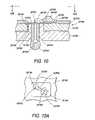
- FIG. 10is a schematic cross sectional view of a semiconductor component having through interconnects
- FIG. 10Ais a schematic cross sectional view taken along section line 10 A- 10 A of FIG. 10 ;
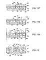
- FIGS. 11A-11Eare schematic cross sectional views illustrating steps in a method for fabricating an encapsulated semiconductor component having through interconnects.
- semiconductor componentmeans an electronic element that includes a semiconductor substrate or makes contact with a semiconductor substrate.
- semiconductor substratemeans an electronic element, such as a semiconductor die, or a semiconductor package that includes integrated circuits and semiconductor devices.
- Interconnectmeans an electrical element which electrically connects different electrical elements and transmits signals between these elements.
- wafer-levelmeans a process conducted on an element, such as a semiconductor wafer, containing multiple semiconductor components or substrates.
- Die levelmeans a process conducted on a singulated element, such as a singulated semiconductor die or package.
- Chip scalemeans having an outline about the same as that of a semiconductor die.
- wafer sizemeans having an outline about the same as that of a semiconductor wafer.
- the semiconductor component 10( FIG. 1A ) includes a semiconductor substrate 12 ( FIG. 1B ); an interposer substrate 14 ( FIG. 1B ); and a transparent substrate 16 ( FIG. 1B ).
- the semiconductor substrate 12( FIG. 1B ) is referred to as the “first substrate”
- the interposer substrate 14( FIG. 1B ) is referred to as the “second substrate”
- the transparent substrate 16( FIG. 1B ) is referred to as the “third substrate”.
- the depth D ( FIG. 1C ) of each substrate opening 36 ( FIG. 1C )is approximately equal to the semiconductor component 10 ( FIG. 1A ).
- the semiconductor component 10comprises a microelectronic imager component.
- the semiconductor substrate 12FIG. 1B
- the semiconductor substrate 12FIG. 1B
- the interposer substrate 14comprises a passive element having no active semiconductor devices.
- alternate embodiment interposer substratescan include active semiconductor devices.
- the transparent substrate 16FIG. 1A
- the transparent substrate 16can include a lens structure configured to focus radiation onto the radiation sensitive integrated circuits in the pixel array 18 . Still further, the transparent substrate 16 can include one or more opaque areas configured to allow specific areas of the pixel array 18 to be accessed.
- the semiconductor substrate 12can comprise another type of semiconductor die having integrated circuits constructed in a desired electrical configuration using active semiconductor devices.
- the semiconductor substrate 12 ( FIG. 1B )can comprise a high speed digital logic device, such as a dynamic random access memory (DRAM), a static random access memory (SRAM), a flash memory, a microprocessor, a digital signal processor (DSP), an application specific integrated circuit (ASIC), a MEMS type device (e.g., accelerometer, microphone, speaker, electro mechanical device), or a solar cell.
- DRAMdynamic random access memory
- SRAMstatic random access memory
- DSPdigital signal processor
- ASICapplication specific integrated circuit
- MEMS type devicee.g., accelerometer, microphone, speaker, electro mechanical device
- both the semiconductor component 10 , and the semiconductor substrate 12can have a generally rectangular chip scale outline with opposed lateral edges and opposed longitudinal edges.
- the semiconductor component 10 and the semiconductor substrate 12can have any polygonal shape, such as square or triangular, and can also have a circular or oval shape.
- the semiconductor substrate 12can comprise a full thickness semiconductor die or a thinned semiconductor die. By way of example a thickness of the semiconductor substrate 12 can be from about 10 ⁇ m to 725 ⁇ m. Since the semiconductor substrate 12 is supported and rigidified by the interposer substrate 14 , it can be made very thin.
- the semiconductor substrate 12includes a circuit side 22 (“first side” in some of the claims), and a back side 24 (“second side” in some of the claims).
- the semiconductor substrate 12includes a plurality of substrate contacts 26 on the circuit side 22 in electrical communication with the integrated circuits 20 ( FIG. 1C ) on the semiconductor substrate 12 .
- the substrate contacts 26can comprise device bond pads, or alternately redistribution contacts (i.e., contacts formed in conjunction with a redistribution layer (RDL)).
- the substrate contacts 26can comprise a highly-conductive, bondable metal, such as aluminum or copper.
- the substrate contacts 26can also comprise stacks of different metals, such as aluminum-nickel-gold, aluminum-nickel-solder, copper-palladium, and aluminum on copper.
- the substrate contacts 26can comprise special purpose contacts.
- the substrate contacts 26can comprise electrically isolated contacts, that are not in electrical communication with the integrated circuits 20 ( FIG. 1C ) on the semiconductor substrate 12 . This concept can be employed in stacked components to reduce unwanted capacitance, noise, bleed off voltage and bleed off current.
- the semiconductor substrate 12( FIG. 1B ) is illustrated with only eight substrate contacts 26 ( FIG. 1A ) arranged in an edge array along the peripheral edges of the semiconductor substrate 12 .
- the semiconductor substrate 12can include tens of substrate contacts 26 ( FIG. 1A ) arranged in a desired configuration, such as a center array, an edge array or an area array.
- the substrate contacts 26 ( FIG. 1A )have a generally square peripheral outline.
- the substrate contacts 26 ( FIG. 1A )can have any polygonal shape including square, rectangular, circular, triangular and oval.
- a size of the substrate contacts 26( FIG.
- each substrate contact 26can have a width on each side of from about 5 ⁇ m to 200 ⁇ m.
- each substrate contact 26can comprise a generally planar pad as shown, or can have other shapes such as a projection, a bump or a volcano shape.
- the substrate contacts 26can be in electrical communication with internal conductors 28 located within the semiconductor substrate 12 proximate to the circuit side 22 .
- the internal conductors 28are in electrical communication with the integrated circuits 20 in the semiconductor substrate 12 .
- the internal conductors 28can be part of the internal structure of the semiconductor substrate 12 , and can comprise a highly conductive metal, such as aluminum or copper.
- an electrical insulation layer 30( FIG. 1C ) on the circuit side 22 protects the internal conductors 28 ( FIG. 1C ) and the integrated circuits 20 ( FIG. 1C ).
- the insulation layer 30( FIG.
- the semiconductor substrate 12can also comprise a tested die that has been certified as a known good die (KGD).
- KGDknown good die
- the semiconductor component 10also includes a plurality of through interconnects 32 , and a plurality of terminal contacts 34 in electrical communication with the through interconnects 32 .
- Each through interconnect 32includes an insulated substrate opening 36 in the semiconductor substrate 12 aligned with an inner surface 44 of an associated substrate contact 26 .
- Each through interconnect 32also includes a projection 38 on a front side 50 of the interposer substrate 14 in mating physical engagement with an associated substrate opening 36 .
- Each through interconnect 32also includes at least one conductive via 40 in the projection 38 having a contact 42 configured for physical and electrical contact with an inner surface 44 of an associated substrate contact 26 .
- the projections 38FIG.
- the conductive vias 40provide separate electrical paths from the substrate contacts 26 ( FIG. 1C ) through the projections 38 ( FIG. 1C ) and the interposer substrate 14 ( FIG. 1C ) to the terminal contacts 34 ( FIG. 1C ).
- the semiconductor substrate 12can also include an electrical insulation layer 46 on the back side 24 thereof extending into the substrate openings 36 of the through interconnects 32 .
- the electrical insulation layer 46can comprise a single layer of material or the substrate openings 36 can include different insulation layers.
- the interposer substrate 14includes an electrical insulation layer 47 on a front side 50 thereof, an electrical insulation layer 48 on a backside 52 thereof, and a pattern of backside conductors 54 on the electrical insulation layer 48 .
- the electrical insulation layers 46 , 47 and 48FIG.
- the interposer substrate 14also includes a plurality of terminal contact pads 56 ( FIG. 1C ) on the electrical insulation layer 48 in electrical communication with the backside conductors 54 ( FIG. 1C ) configured for mounting the terminal contacts 34 to the interposer substrate 14 .
- both the semiconductor substrate 12 ( FIG. 1C ) and the interposer substrate 14 ( FIG. 1C )can comprise silicon, or another semiconductor material such as germanium or gallium arsenide.
- the substrate openings 36 ( FIG. 1C ) in the semiconductor substrate 12 for the through interconnects 32 ( FIG. 1C ), and the projections 38 ( FIG. 1C ) in the interposer substrate 14 for the through interconnects 32 ( FIG. 1C )can be formed with mating sizes and shapes using anisotropic etching processes. With an anisotropic etching process performed on the backside 24 ( FIG. 1C ) of the semiconductor substrate 12 ( FIG. 1C ), each substrate opening 36 ( FIG.
- each projection 38has an angle X° ( FIG. 1C ) measured from the sidewalls of the projections 38 ( FIG. 1C ) and the front side 50 ( FIG. 1C ) of the interposer substrate 14 of about 54.7°.
- the X° angles of 54.7°are due to the different etch rates between the ⁇ 110 ⁇ and the ⁇ 100 ⁇ surfaces of silicon.
- a dry etch processsuch as a Bosch etch, can be used.
- an anisotropic etch process on the semiconductor substrate 12can be performed such that each substrate opening 36 has a generally truncated conical or pyramidal shape recessed into the backside 24 of the semiconductor substrate 12 , and terminating on the inner surface 44 ( FIG. 1C ) of an associated substrate contact 26 .
- an anisotropic etch process on the interposer substrate 14can be performed such that each projection 38 has a generally truncated conical or pyramidal shape projecting from the front side 50 of the interposer substrate 14 .
- both anisotropic etch processescan be performed such that a depth D ( FIG. 1C ) of each substrate opening 36 ( FIG.
- each projection 38is approximately equal to a height H ( FIG. 1C ) of each projection 38 .
- the height H ( FIG. 1C ) of each projection 38can be greater than the depth D ( FIG. 1C ) of each substrate opening 36 ( FIG. 1C ) such that a space is formed between the interposer substrate 14 ( FIG. 1C ) and the semiconductor substrate 12 ( FIG. 1B ).
- a polymer underfill materialcan be placed in the space.
- a representative range for the depth D and the height Hcan be from about 5 ⁇ m to 725 ⁇ m.
- the upper surfaces 58 of the projections 38can have a square peripheral shape, and a width W 1 ( FIG. 1E ), which are approximately equal to, but slightly smaller than the square peripheral shape and the width W 1 ( FIG. 1D ) of the substrate openings 36 ( FIG. 1D ) near the substrate contacts 26 .
- the bases 66 ( FIG. 1D ) of the projectionscan also have a square peripheral shape, and a width W 2 ( FIG. 1E ), which are approximately equal to, but slightly smaller than the square peripheral shape and the width W 2 ( FIG. 1D ) of the substrate openings 36 near the back side 52 ( FIG. 1C ) of the semiconductor substrate 12 .
- a representative range for the width W 1 and the width W 2can be from about 5 ⁇ m to 200 ⁇ m.
- the anisotropic etch processescan also be performed such that the substrate openings 36 ( FIG. 1C ) and the projections 38 ( FIG. 1C ) are almost the same size, but with the projections 38 slightly smaller to permit them to fit into the substrate openings 36 .
- the insulation layer 46 ( FIG. 1C ) in the substrate openings 36 ( FIG. 1C )can be made of a compliant polymeric material, such as polyimide or parylene, to provide a press fit between the projections 38 ( FIG. 1C ) and the substrate openings 36 ( FIG. 1C ).
- the insulation layer 46 ( FIG. 1C )can have a thickness of several microns or more, which is selected to permit some deformation, while still maintaining physical continuity for electrical insulation.
- the insulation layer 46 ( FIG. 1C ) in the substrate openings 36 ( FIG. 1C )can comprise an adhesive material, such that the projections 38 ( FIG. 1C ) adhesively bond to the substrate openings 36 ( FIG. 1C ).
- a separate adhesive layer(not shown) can be deposited on the sidewalls of the substrate openings 36 ( FIG. 1C ), such that the projections 38 ( FIG. 1C ) adhesively bond to the substrate openings 36 ( FIG. 1C ).
- each conductive via 40extends completely through a projection 38 and through the interposer substrate 14 , to the back side 52 of the interposer substrate 14 .
- each projection 38can have multiple conductive vias (e.g., two). However, as shown in FIG. 1B , some of the projections 38 have only one conductive via 40 . In general, depending on space limitations, and the number of electrical paths required by a through interconnect 32 ( FIG. 1C ), each projection 38 can have from one to five conductive vias 40 .
- the conductive vias 40( FIG. 1C ) can comprise an electrically conductive metal, or a conductive polymer, deposited in an electrically insulated via of a selected diameter.
- Each conductive via 40can also include a contact 42 ( FIG. 1C ) configured for physical and electrical contact with the inner surface 44 ( FIG. 1C ) of an associated substrate contact 26 ( FIG. 1C ).
- the contacts 42 ( FIG. 1C ) on the conductive vias 40 ( FIG. 1C )can comprise pads or bumps formed on the top surfaces 58 ( FIG. 1E ) of the projections 38 ( FIG. 1E ), or alternately can comprise the upper planar surfaces of the conductive vias 40 .
- the contacts 42 ( FIG. 1C )can comprise a metal, a solder, or a conductive polymer, that bonds easily to the inner surfaces 44 ( FIG. 1C ) of the substrate contacts 26 ( FIG.
- the contacts 42 of the conductive vias 40can comprise gold, copper, nickel or palladium, metals which bond easily to aluminum.
- the contacts 42can comprise a layer of a conductive polymer, such as a metal filled silicone, or a z-axis epoxy. Suitable conductive polymers are available from A.I. Technology, Trenton, N.J.; Sheldahl, Northfield, Minn.; and 3M, St. Paul, Minn.
- Nano-particle conductive polymersare a nano-particle paste or ink, having metal nano-particles made of a highly conductive metal, such as gold or silver.
- Nano-particle conductive polymersare commercially available from Superior Micropowders, of Albuquerque, N. Mex.
- the backside conductors 54 and the terminal contact pads 56can comprise a same patterned layer of material, such as a highly conductive metal layer (e.g., Cu, Al, Au).
- the terminal contacts 34can comprise metal balls, solder balls, bumps, pins, stud bumps, or insulated wire stud bumps formed on the terminal contact pads 56 using a metallization process, a stud bumping process or a ball bonding process.
- a representative range for the diameter of the terminal contacts 34 ( FIG. 1C )can be from 60-500 ⁇ m.
- the terminal contact pads 56 and the terminal contacts 34can be formed in an area array, such as a ball grid array, a pin grid array, an edge array or a center array.
- FIGS. 2A-2D and 3 A- 3 Csteps in a method for fabricating the semiconductor substrate 12 of the semiconductor component 10 ( FIG. 1A ) are illustrated.
- FIGS. 2A-2D and 3 A- 3 Ca wafer level fabrication process is illustrated.
- the methodcan also be performed at the die level on individual semiconductor substrates 12 .
- a plurality of the semiconductor substrates 12are provided on a semiconductor wafer 64 .
- the semiconductor substrates 12can be provided with the substrate contacts 26 in electrical communication with the integrated circuits 20 ( FIG. 1C ) and with the pixel arrays 18 ( FIG. 3A ).
- the semiconductor substrates 12can be provided with the insulation layers 30 on the circuit sides 22 , and with the substrate contacts 26 embedded in the insulation layers 30 .
- the substrate contacts 26 , the integrated circuits 20 , the pixel arrays 18 , and the insulation layers 30can be fabricated using well known semiconductor fabrication techniques.
- the semiconductor substrate 12can also be thinned from the backside 24 using a suitable process such as grinding, chemical mechanical planarization (CMP) or etching.
- a representative thickness of the semiconductor substrate 12can be from 10 ⁇ m to 725 ⁇ m.
- a mask 60 having mask openings 62can be formed on the backside 24 of the wafer 64 , and an opening forming step can be performed.
- the substrate openings 36FIG. 2C
- the opening forming stepcan be performed such that the substrate contacts 26 maintain their electrical communication with the internal conductors 28 ( FIG. 1C ), and with the integrated circuits 20 ( FIG. 1C ) in the semiconductor substrates 12 .
- the mask 60can comprise a material such as silicon nitride (i.e., hard mask) or resist, deposited to a desired thickness, and then patterned with the mask openings 62 ( FIG. 2B ), using a suitable process.
- the mask 60can be formed using photo patterning equipment configured to form the mask openings 62 ( FIG. 2B ) with a required size and shape, and in precise alignment with the substrate contacts 26 .
- the wafer 64FIG. 3C
- the wafer 64can be held in a temporary carrier 61 ( FIG. 3B ).
- temporary carriers made of glasscan be fused by heat and adhesives to the wafer 64 ( FIG. 3C ) to protect the circuit sides 22 of the semiconductor substrates 12 and permit backside processes such etching, grinding and chemical mechanical planarization (CMP) to be performed.
- CMPchemical mechanical planarization
- Suitable, temporary carriersare manufactured by 3-M Corporation of St. Paul, Minn., and others as well. Because the steps of the method are performed primarily from the backside 24 of the wafer 64 , the circuit side 22 can remain face down and protected by the temporary carrier 61 ( FIG. 3B ).
- the circuit sides 22 of the semiconductor substrates 12can be protected by a removable material such as a tape or mask material applied to the wafer 64 .
- the opening forming stepcan be performed using an anisotropic wet etching process.
- one suitable wet etchantcomprises a solution of KOH and H 2 O.
- KOH etchantan anisotropic etch process is performed, and the substrate openings 36 ( FIG. 2C ) are conical or pyramidal shaped, with sloped sidewalls oriented at an angle of about 54.7° with the respect to the planes of the backsides 24 of the semiconductor substrates 12 .
- the substrate openings 36are illustrated with sloped sidewalls, such as would occur with an anisotropic etch process.
- the thickness of the semiconductor wafer 64is selected, and the anisotropic etch process is controlled, to form the substrate openings 36 with a selected depth D, which will substantially match the height H ( FIG. 1C ) of the projections 38 ( FIG. 1C ).
- the opening forming stepis performed from the backsides 24 of the semiconductor substrates 12 , such that the circuit sides 22 can remain protected.
- the opening forming stepcan be performed with the wafer 64 held in the temporary carrier 61 ( FIG. 3B ).
- the opening forming stepcan be controlled to endpoint the substrate openings 36 ( FIG. 2C ) on the inner surfaces 44 ( FIG. 2C ) of the substrate contacts 26 ( FIG. 2C ).
- the opening forming stepcan be endpointed with the insulation layer 22 covering the inner surfaces 44 ( FIG. 2C ) of the substrate contacts 26 ( FIG. 2C ), which can then be removed by a process such as a chemical etch.
- the insulation layer 22comprises a die passivation layer (e.g., BPSG or SiO 2 ), and the substrate contacts 26 ( FIG. 2C ) comprise the device bond pads, then the substrate contacts 26 ( FIG. 2C ) may in effect be embedded in the insulation layer 22 , which can be removed from the inner surface 44 after the opening 36 has been formed.
- the inner surfaces 44 ( FIG. 2D ) of the substrate contacts 26 ( FIG. 2D )can also be coated with a metal such as solder, nickel or gold, or alternately with a conductive polymer, to facilitate bonding to the contacts 42 ( FIG. 4D ) on the projections 38 ( FIG. 4D ).
- a suitable deposition processsuch as CVD, screen printing or ink jet deposition can be used to coat the inner surfaces 44 ( FIG. 2D ) of the substrate contacts 26 ( FIG. 2D ).
- the substrate openings 36are illustrated as having about the same width W 1 at their intersections with the substrate contacts 26 , as the width W of the substrate contacts 26 . However, if desired, the substrate openings 36 can be smaller or larger in width W 1 than the width W of the substrate contacts 26 . In any case, the substrate openings 36 are preferably formed with a profile that matches the profile of the projections 38 ( FIG. 1C ). In addition, the substrate openings 36 are formed such that the electrical connections between the substrate contacts 26 and the internal conductors 28 ( FIG. 1C ) are maintained.
- the mask 60can be removed from the backside 24 of the wafer 64 , and insulation layers 46 can be formed on the backsides 24 of the semiconductor substrates 12 and in the substrate openings 36 .
- the mask 60can be left on the backside 24 of the wafer 64 as a protective or insulating layer.
- the insulation layers 46can comprise a polymer, such as polyimide or parylene, deposited using a suitable process, such as vapor deposition, capillary injection or screen-printing.
- the insulation layers 46can comprise a deposited oxide layer, such as a low temperature deposited oxide.
- the insulation layers 46can comprise a grown oxide layer, such as silicon dioxide formed by oxidation of silicon.
- FIGS. 4A-4Dsteps in a method for fabricating the interposer substrate 14 of the semiconductor component 10 ( FIG. 1A ) are illustrated.
- a wafer level fabrication processis illustrated.
- the methodcan also be performed at the die level on individual interposer substrates 14 .
- a plurality of the interposer substrates 14are provided on a semiconductor wafer 68 .
- the semiconductor wafer 68can comprise a blank silicon wafer containing no active semiconductor devices.
- the interposer substrates 14are just undefined areas on the semiconductor wafer 68 . Further, at some point in the process illustrated in FIGS.
- the wafer 68can be thinned from the backside using a process such as grinding, chemical mechanical planarization (CMP) or etching to a desired thickness.
- CMPchemical mechanical planarization
- the wafer 68can be held in a temporary carrier (e.g., carrier 61 — FIG. 3B ).
- a representative thickness of the semiconductor wafer 68can be from 10 ⁇ m to 725 ⁇ m.
- an etch mask 70is formed on the front side 50 of the semiconductor wafer 68 , substantially as previously described for etch mask 60 ( FIG. 2B ).
- the etch mask 60has solid areas on the semiconductor wafer 68 , which correspond to the locations of the projections 38 ( FIG. 4B ).
- the solid areas of the etch mask 60have a size which corresponds to the top surfaces 58 ( FIG. 4B ) of the projections 38 ( FIG. 4B ).
- an anisotropic etch processcan be performed substantially as previously described, to etch the projections 38 on the front side 50 of the wafer 68 .
- the projections 38are conical or pyramidal shaped, with sloped sidewalls oriented at an angle of about 54.7° with the respect to the plane of the backsides 52 of the interposer substrates 14 .
- the projections 38are illustrated with sloped sidewalls, such as would occur with an anisotropic etch process.
- the thickness of the semiconductor wafer 68is selected, and the anisotropic etch process is controlled, to form the projections with a selected height H, which will substantially match the depth D ( FIG. 1C ) of the openings 36 ( FIG. 1C ).
- vias 72 for the conductive vias 40are formed through the projections 38 to the back sides of the interposer substrates 14 .
- the vias 72can be formed using a wet or dry etching process.
- the diameters of the vias 72can be from 10 ⁇ m to 2 mils or greater.
- Another method for forming the vias 72uses laser machining followed by etching. In this case the vias 72 will have a generally tapered profile which decreases in a direction farthest from the entry point of the laser.
- a suitable laser system for performing the laser machining stepis manufactured by Electro Scientific, Inc., of Portland, Oreg. and is designated a Model No. 2700.
- a representative laser fluence for forming the vias 72 through a silicon substrate having a thickness of about 28 mils (725 ⁇ m),is from 2 to 10 watts/per opening at a pulse duration of 20-25 ns, and at a repetition rate of up to several thousand per second.
- the wavelength of the laser beamcan be a standard UV wavelength (e.g., 355 nm).
- the insulation layers 47 , 48can be formed substantially as previously described for the insulation layers 46 ( FIG. 2D ).
- the insulation layers 47 , 48can comprise a polymer, such as polyimide or parylene, deposited using a suitable process, such as injection, vapor deposition, capillary wetting, molding, jetting or screen-printing.
- the insulation layers 47 , 48can comprise a deposited oxide layer, such as a low temperature deposited oxide.
- the insulation layers 47 , 48can comprise a grown oxide layer, such as silicon dioxide formed by oxidation of silicon. As also shown in FIG.
- the insulation layers 74can also be formed on the inside diameters of the vias 72 to electrically insulates the vias 72 .
- the insulation layers 74 in the vias 72can comprise an electrically insulating material, such as a polymer (e.g., polyimide or parylene) or an oxide (e.g., SiO 2 ). All of the insulation layers 47 , 48 , 74 are formed such that the vias 72 remain open.
- the insulation layers in the vias 72can be formed separately and the vias 72 reopened as required using an etching or laser machining process.
- the vias 72are at least partially filled with a conductive material to form the conductive vias 40 .
- the conductive vias 40can be plugs that completely fill the vias 72 , or alternately, can be layers that cover just the inside surfaces or sidewalls of the vias 72 .
- the contacts 42 for the conductive vias 40can comprise a same conductive material, or alternately a different conductive material.
- the conductive materialcan comprise a highly conductive metal, such as aluminum, titanium, nickel, iridium, copper, gold, tungsten, silver, platinum, palladium, tantalum, molybdenum, tin, zinc and alloys of these metals including solder alloys.
- the above metalscan be deposited within the vias 72 using a deposition process, such as electroless deposition, CVD, or electrolytic deposition.
- the conductive materialcan comprise a conductive polymer, such as a metal filled silicone, or an isotropic epoxy.
- a conductive polymercan be deposited within the vias 72 , as a viscous material, and then cured as required.
- a suitable deposition processsuch as screen printing, stenciling, or ink jet deposition can be used to deposit the conductive polymer into the vias 72 .
- Suitable conductive polymersare available from A.I. Technology, Trenton, N.J.; Sheldahl, Northfield, Minn.; and 3M, St. Paul, Minn.
- Another suitable conductive polymeris a nano-particle paste or ink, having metal nano-particles made of a highly conductive metal, such as gold or silver. Nano-particle conductive polymers are commercially available from Superior Micropowders, of Albuquerque, N. Mex.
- the back side conductors 54 and the terminal contact pads 56can be formed on the back side 52 of the wafer 68 , using a suitable process such as a metallization process (e.g., etching or deposition through a mask).
- the terminal contacts 34can be formed on the terminal contact pads 56 using a suitable process.
- the terminal contacts 34can comprise metal, or solder balls, bumps or pins, formed on the terminal contact pads 56 using a metallization process, a stud bumping process or a ball bonding process.
- an aligning and placing stepcan be performed.
- the wafers 64 , 68are aligned, and the projections 38 ( FIG. 4D ) on the interposer substrates 14 ( FIG. 4D ) are placed in the openings 36 ( FIG. 2D ) on the semiconductor substrates 12 ( FIG. 2D ).
- the contacts 42 ( FIG. 4D ) on the projections 38 ( FIG. 4D )are placed in physical contact with the inner surfaces 44 ( FIG.
- the aligning and placing stepcan be performed using a suitable tool such as an aligner bonder tool available from a manufacturer such as Karl Suss or EVG.
- a suitable toolsuch as an aligner bonder tool available from a manufacturer such as Karl Suss or EVG.
- one or both of the wafers 64 , 68can be held using temporary carrier (e.g., carrier 61 — FIG. 3B ).
- a bonding stepcan optionally be performed to bond the contacts 42 ( FIG. 2D ) on the projections 38 ( FIG. 4D ) to the inner surfaces 44 ( FIG. 2D ) of the substrate contacts 26 ( FIG. 2D ).
- the bonding stepcan be performed using heat, pressure, ultrasonic vibrations, or by depositing and curing a conductive adhesive material.
- the contacts 42 ( FIG. 2D )can comprise a metal such as gold or solder that is heated to metallurgically bond to the substrate contacts 26 ( FIG. 2D ) made of aluminum.
- a cold weldsuch as a gold to gold diffusion bond can be formed.
- the contacts 42can comprise a conductive polymer that is deposited in viscous form using a process such as ink jet deposition, and then cured in contact with the substrate contacts 26 ( FIG. 2D ).
- the inner surfaces 44 ( FIG. 2D ) of the substrate contacts 26 ( FIG. 2D )can be coated with a metal such as solder, nickel or gold to facilitate bonding to the contacts 42 ( FIG. 4D ) on the projections 38 ( FIG. 4D ).
- the projections 38 ( FIG. 4D ) in the interposer substrate 14can be sized relative to the openings 36 ( FIG. 2D ) in the semiconductor substrate 12 such that a gap is formed which can be filled with a polymer underfill material which also adhesively bonds the interposer substrate 14 and the semiconductor substrate 12 .
- a singulating stepcan be performed in which the bonded wafers 64 ( FIG. 2D) and 68 ( FIG. 4D ) and the bonded substrates 12 ( FIG. 2D ), 14 ( FIG. 4D ) are singulated into individual components 10 ( FIG. 1A ).
- the singulating stepcan be performed using a dicing saw configured to dice semiconductor wafers into individual dice. Alternately rather than by sawing, the singulating step can be performed using another singulation method, such as cutting with a laser or a water jet, or by etching with a suitable wet or dry etchant. Either prior to, or alternately after the singulating step, the transparent substrate 16 can be attached to the semiconductor substrate 12 using techniques that are known in the art.
- the stacked die semiconductor component 10 Aincludes a first semiconductor substrate 12 A ( FIG. 5B ), and a second semiconductor substrate 12 B ( FIG. 5B ).
- the stacked die semiconductor component 10 Ais substantially similar to the semiconductor component 10 ( FIG. 1A ) but with the interposer substrate 14 ( FIG. 1B ) replaced by the second semiconductor substrate 12 B ( FIG. 5B ).
- the first semiconductor substrate 12 A ( FIG. 5B )includes integrated circuits 20 A ( FIG. 5B )
- the second semiconductor substrate 12 B ( FIG. 5B )also includes integrated circuits 20 B ( FIG. 5A ).
- the first semiconductor substrate 12 A ( FIG. 5B )includes integrated circuits 20 A ( FIG. 5B )
- the second semiconductor substrate 12 BFIG. 5B
- the first semiconductor substrate 12 AFIG.
- electrical insulation layers 30 A, 46 A, 47 B, 48 Binsulate the major planar surfaces of the first semiconductor substrate 12 A ( FIG. 5B ) and the second semiconductor substrate 12 B ( FIG. 5B ).
- the first semiconductor substrate 12 A and the second semiconductor substrate 12 Bcan have different electrical configurations.
- the first semiconductor substrate 12 Acan comprise a memory device (e.g., DRAM)
- the second semiconductor substrate 12 Bcan comprise a processor or an application specific integrated circuit (ASIC).
- both the first semiconductor substrate 12 A and the second semiconductor substrate 12 Bcan comprise a selected high speed digital logic device selected from the group consisting of a dynamic random access memory (DRAM), a static random access memory (SRAM), a flash memory, a microprocessor, a digital signal processor (DSP), an application specific integrated circuit (ASIC), or a MEMS type device.
- DRAMdynamic random access memory
- SRAMstatic random access memory
- DSPdigital signal processor
- ASICapplication specific integrated circuit
- both the first semiconductor substrate 12 A and the second semiconductor substrate 12 Bcan comprise known good dice (KGD). Still further, both the first semiconductor substrate 12 A and the second semiconductor substrate 12 B can have a desired thickness, and can comprise thinned dice as previously described. Also, the first semiconductor substrate 12 A can be made very thin because it is protected and rigidified by the second semiconductor substrate 12 B. A representative thickness for the first semiconductor substrate 12 A and the second semiconductor substrate 12 B can be from 10 ⁇ m to 725 ⁇ m.
- the first semiconductor substrate 12 Aalso includes a plurality of substrate contacts 26 A on its circuit side 22 A.
- the substrate contacts 26 Acan comprise the device bond pads, or redistribution (rdl) contacts, in electrical communication with the internal conductors 28 A ( FIG. 5A ) and the integrated circuits 20 A ( FIG. 5A ) on the first semiconductor substrate 12 A.
- the stacked die semiconductor component 10 Aalso includes through interconnects 32 A in electrical communication with the backsides of the substrate contacts 26 A on the first semiconductor substrate 12 A, substantially as previously described for through interconnects 32 ( FIG. 1C ).
- Each through interconnect 32 A( FIG. 5B ) includes an insulated substrate opening 36 A ( FIG. 5B ) in the semiconductor substrate 12 A aligned with the backside of an associated substrate contact 26 A ( FIG. 5B ).
- Each through interconnect 32 Aalso includes a projection 38 A ( FIG. 5B ) on a back side 24 B ( FIG. 5B ) of the second semiconductor substrate 12 B ( FIG. 5B ) configured for mating physical engagement with an associated substrate opening 36 A ( FIG. 5B ) in the first semiconductor substrate 12 A ( FIG. 5B ).
- Each through interconnect 32 A ( FIG. 5B )also includes at least one conductive via 40 A ( FIG. 5B ) in the projection 38 A having a contact configured for physical and electrical contact with a backside of an associated substrate contact 26 A ( FIG. 5B ).
- the second semiconductor substrate 12 Balso includes a plurality of substrate contacts 26 B on its circuit side 22 B ( FIG. 5B ).
- the substrate contacts 26 Bcan comprise the device bond pads, or redistribution (rdl) contacts, in electrical communication with the internal conductors 28 B ( FIG. 5A ) and the integrated circuits 20 B ( FIG. 5A ) on the second semiconductor substrate 12 B.
- the second semiconductor substrate 12 B( FIG. 5A ) also includes conductors 54 A ( FIG. 5A ), terminal contact pads 56 A ( FIG. 5A ) and terminal contacts 34 A ( FIG. 5A ) on the circuit side 22 B thereof. With this arrangement, the conductors 54 A ( FIG.
- the stacked die semiconductor component 10 Acan be fabricated using a wafer level process, or a die level fabrication process, substantially as previously described for semiconductor component 10 ( FIG. 1B ).
- the first semiconductor substrate 12 A( FIG. 5B ) can be fabricated substantially as previously described and shown in FIGS. 2A-2D for the semiconductor substrate 12 ( FIG. 1B ).
- the second semiconductor substrate 12 B( FIG. 5B ) can be fabricated substantially as previously described and shown in FIGS. 4A-4D for the interposer substrate 14 ( FIG. 1B ).
- an additional insulation layer(not shown) can be formed on the circuit side 22 A ( FIG. 5B ) of the first semiconductor substrate 12 A ( FIG. 5B ).
- stacking contactscan be formed on the substrate contacts 26 A ( FIG. 5B ) of the first semiconductor substrate 12 A ( FIG. 5B ).
- the terminal contacts 34 Acan be formed on the substrate contacts 26 A on the circuit side 22 A of the first semiconductor substrate 12 A.
- the semiconductor component 10 Iincludes a semiconductor substrate 12 I having substrate contacts 26 I in electrical communication with integrated circuits substantially as previously described for substrate 12 ( FIG. 1A ).
- the semiconductor component 10 Ialso includes an interposer substrate 14 I having terminal contact pads 56 I and terminal contacts 34 I, substantially as previously described for interposer substrate 14 ( FIG. 1B ).
- the semiconductor component 10 Ialso includes an encapsulant 76 on the circuit side of the semiconductor substrate 12 I, which encapsulates the substrate contacts 26 I.
- the semiconductor component 10 Ialso includes a plurality of through interconnects 32 I, which are substantially similar to the previously described through interconnects 32 ( FIG. 1B ).
- the through interconnects 32 Iinclude substrate openings 36 I that are isotropically etched in the semiconductor substrate 12 I. With an isotropic etch process, the substrate openings 36 I, rather than being conical or pyramidally shaped, are generally hemispherical or concave in shape.
- the through interconnects 32 Iinclude projections 38 I that are isotropically etched on the interposer substrate 14 I. With an isotropic etch process, the projections 38 I, rather than being conical or pyramidally shaped, are generally radiused or convex in shape.
- the isotropic projections 38 I ( FIG. 6 ) and the isotropic substrate openings 36 I ( FIG. 6 )are configured for mating physical engagement.
- the substrate openings 36 I ( FIG. 6 )are generally hemispherical or concave, and the projections 38 I ( FIG. 6 ) are generally radiused or convex in shape, the projections 38 I ( FIG. 6 ) do not fit precisely into the substrate openings 36 I ( FIG. 6 ).
- the through interconnects 32 Ialso include conductive vias 40 I ( FIG. 6 ) through the projections 38 I ( FIG. 6 ), that are in electrical contact with the substrate contacts 26 I ( FIG. 6 ) on the circuit side of the semiconductor substrate 12 I ( FIG. 6 ), and with the terminal contact pads 56 I ( FIG. 6 ) on the back side of the interposer substrate 14 I ( FIG. 6 ).
- the semiconductor substrate 12 I( FIG. 6 ) can be fabricated substantially as shown and described in FIGS. 2A-2D for semiconductor substrate 12 ( FIG. 2D ).
- the interposer substrate 14 I( FIG. 6 ) can be fabricated substantially as shown and described in FIGS. 4A-4D for interposer substrate 14 ( FIG. 4D ).
- an isotropic etch processcan be used to form the substrate openings 36 I ( FIG. 6 )
- an isotropic etch processcan be used to form the projections 38 I ( FIG. 6 ).
- one suitable etchant for performing isotropic etch processesis a solution of HF, HNO 3 and H 2 O.
- the multiple die stack semiconductor component 10 Sincludes a first semiconductor substrate 12 S ⁇ 1, and a second semiconductor substrate 12 S ⁇ 2, which are substantially identical in construction.
- the semiconductor component 10 Scan include any number of stacked semiconductor substrates (e.g., 2 to 20 ).
- the semiconductor substrates 12 S ⁇ 1, 12 S ⁇ 2include substrate contacts 26 S on their circuit sides 22 S ( FIG. 7 ) in electrical communication with the integrated circuits contained in the semiconductor substrates 12 S ⁇ 1, 12 S ⁇ 2.
- the semiconductor substrates 12 S ⁇ 1, 12 S ⁇ 2also include electrical insulation layers 30 S ( FIG. 7 ) on their circuit sides 22 S ( FIG. 7 ), and electrical insulation layers 46 S ( FIG.
- the semiconductor substrates 12 S ⁇ 1, 12 S ⁇ 2also include through interconnects 32 S ( FIG. 7 ), which comprise insulated substrate openings 36 S ( FIG. 7 ), projections 38 S ( FIG. 7 ) and conductive vias 40 S ( FIG. 7 ).
- each semiconductor substrate 12 S ⁇ 1, 12 S ⁇ 2includes both insulated substrate openings 36 S and projections 38 S.
- the conductive vias 40 Scan comprise metal layers, which extend between the insulated substrate openings 36 S and the projections 38 S, and at least partially cover the tip portions of the projections 38 S.
- the semiconductor component 10 Scan be rigidified by filling the substrate openings 36 S ( FIG. 7 ) with a polymer material such as an underfill polymer.
- the semiconductor substrates 12 S ⁇ 1, 12 S ⁇ 2are stacked circuit side 22 S to back side 24 S, such that the substrate contacts 26 S on the second semiconductor substrate 12 S ⁇ 2 physically and electrically contact the projections 38 S on the first semiconductor substrate 12 S ⁇ 1.
- the substrate contacts 26 S on the second semiconductor substrate 12 S ⁇ 2can be bonded to the conductive vias 40 S on the first semiconductor substrate 12 S ⁇ 1, substantially as previously described for the contacts 42 ( FIG. 1C ) on the conductive vias 40 ( FIG. 1C ).
- the openings 36 S ( FIG. 7 ) between adjacent semiconductor substrates 12 S ⁇ 1, 12 S ⁇ 2can be filled with a polymer material such as silicone, polyimide or an underfill polymer.
- the openings 36 S ( FIG. 7 ) in the semiconductor substrates 12 S ⁇ 1, 12 S ⁇ 2can be fabricated using an anisotropic etch process, substantially as previously described for the openings 36 ( FIG. 1C ) in the semiconductor substrate 12 ( FIG. 1C ).
- the projections 38 S ( FIG. 7 ) on the semiconductor substrates 12 S ⁇ 1, 12 S ⁇ 2can also be fabricated using an anisotropic etch process, substantially as previously described for the projections 38 ( FIG. 1C ) in the interposer substrate 14 ( FIG. 1C ). In this case, two etch processes can be performed on the same substrate using two separate etch masks.
- the conductive vias 40 Scan be fabricated using a suitable metallization process (e.g., deposition through a mask).
- the semiconductor component 10 S( FIG. 7 ) can be constructed with the semiconductor substrates 12 S ⁇ 1, 12 S ⁇ 2 having different electrical configurations, such that a system in a package can be provided.
- some of the semiconductor substrates in a stackcan comprise memory devices, and some of the semiconductor substrates in the stack can comprise processing devices or application specific devices.
- the semiconductor component 10 Pincludes a semiconductor substrate 12 P having substrate contacts 26 P in electrical communication with integrated circuits, substantially as previously described for substrate 12 ( FIG. 1A ).
- the semiconductor component 10 Palso includes an interposer substrate 14 P having terminal contact pads 56 P and terminal contacts 34 P, substantially as previously described for interposer substrate 14 ( FIG. 1B ).
- the semiconductor component 10 Palso includes a plurality of through interconnects 32 P ( FIG. 9 ), which are substantially similar to the previously described through interconnects 32 ( FIG. 1B ).
- the through interconnects 32 Pinclude substrate openings 36 P ( FIG. 9 ) having generally cylindrical shapes, and projections 38 P ( FIG. 9 ) comprising cylindrical pins having mating cylindrical shapes configured to fit into the substrate openings 36 P.
- the projections 38 Pcan also be adhesively bonded to the substrate openings 36 P ( FIG. 9 ).
- the substrate openings 36 P ( FIG. 9 )can be formed in the semiconductor substrate 12 P ( FIG.
- the projections 38 P ( FIG. 9 )can also be formed on the interposer substrate 14 P made of silicon, using a dry etch process (e.g., Bosch etch), substantially as previously described for projections 38 ( FIG. 1C ).
- a dry etch processe.g., Bosch etch
- the through interconnects 32 P ( FIG. 9 )also include conductive vias 40 P ( FIG. 9 ) through the projections 38 P ( FIG. 9 ) in electrical communication with the substrate contacts 26 P ( FIG. 9 ), and with the terminal contact pads 56 P ( FIG. 9 ).
- the semiconductor component 10 TWI( FIG. 10 ) includes a semiconductor substrate 12 TWI ( FIG. 10 ) having substrate contacts 26 TWI ( FIG. 10 ) in electrical communication with integrated circuits, substantially as previously described for substrate 12 ( FIG. 1A ).
- the substrate contacts 26 TWI( FIG. 10 ) are embedded in an electrical insulation layer 30 TWI ( FIG. 10 ) having openings 86 TWI ( FIG. 10 ), that align with the substrate contacts 26 TWI ( FIG. 10 ).
- the substrate contacts 26 TWI( FIG. 10 ) can comprise device bond pads, or redistribution layer (rdl) pads.
- the electrical insulation layer 30 TWI( FIG. 10 ) can comprise a die passivation layer, or a redistribution insulating layer.
- the semiconductor component 10 TWIalso includes an interposer substrate 14 TWI ( FIG. 10 ) having terminal contacts 34 TWI ( FIG. 10 ), substantially as previously described for the interposer substrate 14 ( FIG. 1B ).
- the semiconductor component 10 TWIincludes a plurality of through interconnects 32 TWI ( FIG. 10 ), that are substantially similar to the previously described through interconnects 32 P ( FIG. 9 ).
- the through interconnects 32 TWIinclude cylindrical openings 36 TWI ( FIG. 10 ) in the semiconductor substrate 12 TWI ( FIG. 10 ) aligned with the substrate contacts 26 TWI ( FIG. 10 ).
- the through interconnects 32 TWIFIG.
- FIG. 10also include cylindrical pin projections 38 TWI ( FIG. 10 ) in the interposer substrate 14 TWI ( FIG. 10 ), that mate with the cylindrical openings 36 TWI ( FIG. 10 ) in the semiconductor substrate 12 TWI ( FIG. 10 ), substantially as previously described.
- the through interconnects 32 TWIalso include conductive vias 40 TWI ( FIG. 10 ) that comprise through wire interconnects (TWI).
- the conductive vias 40 TWIcan be constructed substantially as described in U.S. application Ser. No. 11/296,057, filed on Dec. 7, 2005, entitled “Semiconductor Components Having Through Wire Interconnects (TWI), And Method And Systems For Fabricating Semiconductor Components”, and in U.S. application Ser. No. 11/102,408, filed on Apr. 8, 2005, entitled “Method And System For Fabricating Semiconductor Components With Through Wire Interconnects”, both of which are incorporated herein by reference.
- Each conductive via 40 TWIincludes a via 72 TWI ( FIG. 10 ) through a substrate contact 26 TWI ( FIG. 10 ) on the semiconductor substrate 12 TWI ( FIG. 10 ), and through a projection 38 TWI ( FIG. 10 ) in the interposer substrate 14 TWI ( FIG. 10 ).
- Each conductive via 40 TWI ( FIG. 10 )also includes a wire 80 TWI ( FIG. 10 ) in the via 72 TWI ( FIG. 10 ), and a bonded connection 82 TWI ( FIG. 10 ) between the wire 80 TWI ( FIG. 10 ) and the substrate contact 26 TWI ( FIG. 10 ).
- Each conductive via 40 TWI ( FIG. 10 )can also include a bonding member 72 TWI ( FIG. 10 ) on the wire 80 TWI ( FIG. 10 ) and the substrate contact 26 TWI ( FIG. 10 ), and a dielectric material 88 TWI ( FIG. 10 ) in the via 36 TWI ( FIG. 10 ).
- the via 72 TWIextends through the substrate contact 26 TWI ( FIG. 10 ), and through the full thickness of the interposer substrate 14 TWI ( FIG. 10 ). As shown in FIG. 10A , the via 72 TWI ( FIG. 10 ) can be offset from the center line of the substrate contacts 26 TWI, such as in the left hand corner thereof.
- the via 72 TWI ( FIG. 10 )is generally circular, and has an inside diameter (ID) which is about 1.5 to 3 times larger than the outside diameter (OD) of the wire 80 TWI ( FIG. 10 ).
- IDinside diameter
- ODoutside diameter
- the wire 80 TWIFIG. 10
- the wire 80 TWIcan have an outside diameter (OD) of about 25 ⁇ m
- the via 72 TWIcan also include an insulating layer 74 TWI ( FIG. 10 ) formed on an inside diameter thereof, substantially as previously described.
- the bonded connection 82 TWI( FIG. 10A ) can be formed between a first end of the wire 80 TWI ( FIG. 10 ) and the substrate contact 26 TWI ( FIG. 10 ).
- the bonded connection 82 TWI( FIG. 10 ) can comprise a ball bond formed using a wire bonding process, such as thermosonic wire bonding, or alternately a wedge bond formed using ultrasonic wire bonding.
- the second end of the wire 80 TWI ( FIG. 10 )can include a generally spherically shaped contact ball 90 TWI ( FIG. 10 ), such as a “free air ball” formed using an electronic flame off (EFO) process.
- EFOelectronic flame off
- the terminal contact 34 TWI( FIG. 10 ) can be formed directly on the contact ball 90 TWI ( FIG.
- the contact ball 90 TWI( FIG. 10 ) can be omitted, and the terminal contact 34 TWI ( FIG. 10 ) formed directly on the end of the wire 80 TWI ( FIG. 10 ).
- the wire 80 TWI ( FIG. 10 ) and the bonding member 84 TWI ( FIG. 10 ) as well,can include a metal coating such as an electrolessly deposited metal such as Ni or Pd on Al configured to stiffen the wire 80 TWI ( FIG. 10 ) and increase the height of the bonding member 84 TWI ( FIG. 10 ).
- the dielectric material 88 TWI( FIG. 10 ) is configured to surround, insulate and secure the wire 80 TWI ( FIG. 10 ) in the via 72 TWI ( FIG. 10 ).
- the dielectric material 88 TWI ( FIG. 10 )can comprise a polymer material such as polyimide, deposited using a suitable process, such as deposition through a nozzle, or deposition using a material dispensing system. For some applications the dielectric material 88 TWI ( FIG. 10 ) can be omitted.
- the bonding member 84 TWI( FIG. 10 ) is configured to secure the wire 80 TWI ( FIG. 10 ) to the substrate contact 26 TWI ( FIG. 10 ), and to provide a bonding structure for bonding the semiconductor component 10 TWI ( FIG.
- the bonding member 84 TWIcan comprise a stud bump, or a ball bump formed using a wire bonder, a stud bumper, or a ball bumper.
- the bonding member 84 TWIcan comprise a solder joint, a welded connection, or a conductive polymer connection, formed using a bonding process, such as thermal or pressure bonding.
- the bonding member 84 TWIcan be omitted.
- the semiconductor substrate 12 TWI ( FIG. 10 ) and the interposer substrate 14 TWI ( FIG. 10 ),can be fabricated, then aligned and placed together substantially as previously described.
- the conductive via 40 TWI ( FIG. 10 )can be fabricated by forming the via 72 TWI ( FIG. 10 ) through the substrate contact 26 TWI ( FIG. 10 ), and part way through the interposer substrate 14 TWI ( FIG. 10 ), then placing the wire 80 TWI ( FIG. 10 ) in the via 40 TWI ( FIG. 10 ), and the bonding the wire 80 TWI ( FIG. 10 ) to the substrate contact 26 TWI ( FIG. 10 ) to form the bonded connection 82 TWI ( FIG. 10 ).
- the fabrication methodcan also includes the step of placing the dielectric material 88 TWI ( FIG. 10 ) in the via 72 TWI ( FIG. 10 ).
- the dielectric material 88 TWI ( FIG. 10 )can comprise an electrically insulating curable polymer, such as a polyimide, an epoxy or a silicone. Suitable curable polymers are manufactured by Shinitsu of Japan, and Dexter Electronic Materials of Rocky Hill, Conn.
- the dielectric material 88 TWI ( FIG. 10 )provides a potting structure which secures and electrically insulates the wire 80 TWI ( FIG. 10 ) in the via 40 TWI ( FIG. 10 ).
- the dielectric material 80 TWI( FIG. 10 ) can be injected into the via 40 TWI ( FIG. 10 ) in a viscous state, pulled by capillary action by vacuum directed through a vent, and then cured.
- a positive displacement mechanismsuch as a syringe, can be used to dispense a quantity of the dielectric material 80 TWI ( FIG. 10 ) in a viscous state into the via 40 TWI ( FIG. 10 ).
- Other suitable deposition processes for depositing the dielectric material 80 TWI ( FIG. 10 ) into the via 40 TWI ( FIG. 10 )include screen printing, stenciling and stereographic lithography.
- the dielectric material 80 TWI ( FIG. 10 )can also be deposited into the via 40 TWI ( FIG. 10 ) using a film assisted molding equipment (FAME) process to be further described.
- FAMEfilm assisted molding equipment
- the fabrication methodcan also includes the steps of thinning the interposer substrate 14 TWI ( FIG. 10 ) from the back side to expose the contact ball 90 TWI ( FIG. 10 ), and then forming the bonding member 84 TWI ( FIG. 10 ) on the bonded connection 82 TWI ( FIG. 10 ) and the substrate contact 26 TWI ( FIG. 10 ). Further details of the fabrication process are disclosed in the previously incorporated U.S. application Ser. Nos. 11/296,057 and 11/102,408.
- the semiconductor components 10( FIG. 1A ), 10 A ( FIG. 5A ), 10 I ( FIG. 6 ), 10 S ( FIG. 7 ), 10 P ( FIG. 9 ) or 10 TWI ( FIG. 10 ) can be used as stand alone devices, or in combination with other semiconductor components to fabricate semiconductor systems 78 ( FIG. 8 ).
- the semiconductor systems 78 ( FIG. 8 )can include singulated components bonded to one another (singulated system), or singulated semiconductor components bonded to a semiconductor wafer (wafer system), or semiconductor components contained on a semiconductor wafer bonded to another semiconductor wafer (wafer to wafer system).
- the through interconnects 32( FIG. 1B ), 32 A ( FIG. 5B ), 32 I ( FIG. 6 ), 32 S ( FIG. 7 ), 32 P ( FIG. 9 ), or 32 TWI ( FIG. 10 ) provide a signal transmission system, and bonding structures between adjacent stacked components and next level substrates as well.
- FIGS. 11A-11Isteps in a method for fabricating an encapsulated semiconductor component 10 E ( FIG. 11I ) with through interconnects 32 E ( FIG. 11I ) is illustrated.
- a semiconductor wafer 68 E containing a plurality of semiconductor substrates 12 Ecan be provided.
- the semiconductor substrates 12 Einclude integrated circuits, and substrate contacts 26 E in electrical communication with the integrated circuits, substantially as previously described for the semiconductor substrate 12 ( FIG. 1B ).
- the semiconductor substrates 12 Ealso include substrate openings 36 E aligned with the substrate contacts 26 E, substantially as previously described for any of the previously described substrate openings (e.g., 36 — FIG. 2C ).
- the singulated semiconductor substrates 14 Ecan comprise semiconductor dice, such as known good dice (KGD), having integrated circuits in a desired electrical configuration (e.g., DRAM).
- the singulated semiconductor substrates 14 Ealso include projections 38 E ( FIG. 11A ) having conductive vias 40 E ( FIG. 11A ) in electrical contact with the substrate contacts 26 E ( FIG. 11A ) on the semiconductor substrates 12 E ( FIG. 11A ).
- the projections 38 EFIG.
- the conductive vias 40 Ecan be substantially similar to any of the previously described projections (e.g., 38 , 38 A, 38 I, 38 S, 38 P, 38 TWI).
- the conductive vias 40 Ecan be substantially similar to any of the previously described conductive vias (e.g., 40 , 40 A, 40 I, 40 S, 40 P, 40 TWI).
- the through interconnects 32 Ecan be substantially similar to any of the previously described through interconnects (e.g., 32 , 32 A, 32 S, 32 P, 32 TWI). However in this embodiment, the projections 38 E ( FIG. 11A ) and the substrate openings 36 E ( FIG. 11A ) are configured such that spaces 92 E ( FIG. 11A ) are formed between the singulated semiconductor substrates 14 E ( FIG. 11A ) and the semiconductor wafer 68 E ( FIG. 11A ).
- the singulated semiconductor substrates 14 Ecan be placed on the semiconductor wafer 68 E ( FIG. 11A ), such that spaces 94 E ( FIG. 11A ) are also formed between the semiconductor substrates 14 E ( FIG. 11A ).
- the singulated semiconductor substrates 14 E ( FIG. 11A )can be placed on the semiconductor wafer 68 E ( FIG. 11A ) using an alignment device, a pick and place mechanism, or other suitable apparatus.
- U.S. Pat. No. 7,060,526 to Farnworth et al.which is incorporated herein by reference, further describes processes for mounting singulated dice to a base wafer, and additional processes as well, which are similar to steps of the present method.
- the conductive vias 40 Ecan be bonded to the substrate contacts 26 E ( FIG. 11A ), substantially as previously described for any of the previously described through interconnects (e.g., 32 , 32 A, 32 S, 32 P, 32 TWI).
- a polymer fill stepis performed in which an underfill polymer 96 E ( FIG. 11B ) is placed in the spaces 92 E ( FIG. 11A ) between the singulated substrates 14 E and the semiconductor wafer 68 E, and in the spaces 94 E ( FIG. 11A ) between the singulated semiconductor substrates 14 E ( FIG. 11A ).
- the underfill polymer 96 E ( FIG. 11B )functions to bond the singulated semiconductor substrates 14 E ( FIG. 11B ) to the semiconductor wafer 68 E ( FIG. 11B ).
- the underfill polymer 96 E ( FIG. 11B )encapsulates the edges of the completed semiconductor components 10 E ( FIG. 1I ).
- the underfill polymer 96 Ecan comprise a conventional underfill polymer such as a curable silicone, epoxy or polyimide material.
- suitable underfill polymer materialsare manufactured by Dexter Electronic Materials, City of Industry, Calif. under the trademark “HYSOL”.
- the underfill polymer 96 Ecan be deposited on the semiconductor wafer 68 E ( FIG. 11B ) in a viscous state using a conventional deposition apparatus, such as a material dispensing system having a computer controlled nozzle.
- a material dispensing systemhaving a computer controlled nozzle.
- One suitable systemis manufactured by Asymtek of Carlsbad, Calif.
- one or more damscan be formed on the semiconductor wafer 68 E ( FIG. 11B ) for containing the viscous underfill polymer material.
- a pressure chambercan be used to distribute and draw the under fill polymer 96 E ( FIG. 11B ) into the spaces 92 E, 94 E ( FIG. 11A ) using vacuum and pressure.
- the underfill polymer 96 E ( FIG. 11B )can then be cured using a suitable curing process.
- a planarizing and thinning stepcan be performed to planarize and thin the singulated semiconductor substrates 14 E ( FIG. 11C ) to a common plane 98 E.
- This stepcan be performed using a suitable process, such as grinding, chemical mechanical planarization (CMP) or etching.
- a representative thickness of the singulated semiconductor substrate 14 Ecan be from 10 ⁇ m to 725 ⁇ m.
- the semiconductor wafer 68 Ecan be flipped, and a first encapsulation step can be performed.
- the first encapsulation stepcan be performed using a compression mold process, such as a film assisted molding equipment (FAME) process.
- FAMEfilm assisted molding equipment
- Equipment for performing film assisted molding equipment (FAME)is available from Boschman Industries of Holland, and APIC Yamada America, Chandler, Ariz.
- FAMEfilm assisted molding equipment
- a clamp ring, a release film, and a compression mold systemcan be used to mold a first encapsulating layer 100 E ( FIG. 11D ), which encapsulates the singulated semiconductor substrates 14 E ( FIG. 11D ) on the semiconductor wafer 68 E ( FIG. 11D ).
- the first encapsulating layer 100 E( FIG. 11D ) can initially comprise a suitable powder mold compound that is placed on the semiconductor wafer 68 E ( FIG. 11D ) and then compression molded to a desired shape.
- soluble eye point dams(not shown) can cover alignment marks on the semiconductor wafer 68 E ( FIG. 11D ), and can be removed following formation of the first encapsulating layer 100 E ( FIG. 11D ) to provide alignment of the semiconductor wafer 68 E during subsequent processing.
- the through interconnects 32 E( FIG. 11D ) comprise through wire interconnects (e.g., 32 TWI— FIG. 10 )
- the first encapsulating layer 100 Ecan also be molded into vias (e.g., 72 TWI— FIG.
- a representative thickness of the first encapsulating layer 100 Ecan be from 25 ⁇ m to 150 ⁇ m. Following the compression molding process, the first encapsulating layer 100 E can be cured using a suitable process.
- contact bumps 104 Eare formed on the substrate contacts 26 E ( FIG. 11E ), or alternately on redistribution pads (not shown), in electrical communication with the substrate contacts 26 E ( FIG. 1E ).
- the contact bumps 104 Ecan comprise metal bumps deposited on the substrate contacts 26 E ( FIG. 11E ) using a suitable deposition process, such as stenciling and reflow of a metal alloy onto the substrate contacts 26 E ( FIG. 11E ).
- the contact bumps 104 E ( FIG. 11E )can comprise solder, another metal such as Cu, Au or Ni, or a conductive polymer material.
- a scribing stepcan be performed in which grooves 106 E ( FIG. 11E ) are formed in the semiconductor wafer 68 E ( FIG. 11E ) in the streets between the individual semiconductor substrates 12 E ( FIG. 11E ) on the semiconductor wafer 68 E ( FIG. 11E ).
- the scribing stepcan be performed using a dicing saw having saw blades set to penetrate through the semiconductor wafer 68 E ( FIG. 11E ) to the polymer underfill layer 96 E ( FIG. 11E ).
- the scribing stepcan also be performed by etching the grooves 106 E ( FIG.
- a second encapsulating stepcan be performed to form a second encapsulating layer 102 E ( FIG. 11F ) on the circuit side of the semiconductor wafer 68 E ( FIG. 11F ).
- the second encapsulating layer 102 E ( FIG. 11F )also encapsulates the contact bumps 104 E ( FIG. 11F ), and fills the grooves 106 E ( FIG. 11F ) formed during the scribing step.
- the second encapsulating stepcan be performed using a film assisted molding equipment (FAME) process substantially as previously described for forming the first encapsulating layer 100 E ( FIG. 11F ).
- FAMEfilm assisted molding equipment
- a second planarizing stepis performed to planarize the contact bumps 104 E ( FIG. 11G ) and the second encapsulating layer 102 E ( FIG. 11G ) to a common planar surface.
- This stepcan be performed using suitable process such as grinding, chemical mechanical planarization (CMP) or etching, substantially as previously described for the planarizing and thinning step ( FIG. 1C ).
- CMPchemical mechanical planarization
- etchingsubstantially as previously described for the planarizing and thinning step ( FIG. 1C ).
- FIG. 1Cplanarizing and thinning step
- terminal contacts 34 E( FIG. 11H ) are formed on the planarized contact bumps 104 E ( FIG. 11H ).
- the terminal contacts 34 E( FIG. 11H ) are also sometimes referred to in the art as outer lead bonds (OLB).
- the through interconnects 32 E( FIG. 11H ) are sometimes referred to as the inner lead bonds (ILB).
- the terminal contacts 34 E ( FIG. 11H )can comprise metal, or solder, balls, bumps or pins, formed using a metallization process, a stud bumping process or a ball bonding process.
- a representative range for the diameter of the terminal contacts 34 E ( FIG. 11H )can be from 60-500 ⁇ m.
- a singulating stepcan be performed in which singulating cuts 108 E ( FIG. 1H ) are formed through the first and second encapsulating layers 100 E, 102 E ( FIG. 1H ), through the polymer filled grooves 106 E ( FIG. 1H ) and through the polymer underfill layer 96 E ( FIG. 1H ).
- the singulating stepcan be performed using a dicing saw configured to dice semiconductor wafers into individual dice. Alternately, rather than by sawing, the singulating step can be performed using another singulation method, such as cutting with a laser or a water jet, or by etching with a suitable wet or dry etchant.
- each semiconductor component 10 Eincludes a first semiconductor substrate 12 E ( FIG. 11I ) and a second semiconductor substrate 14 E ( FIG. 11I ) bonded to one another by the polymer underfill layer 96 E ( FIG. 11B ).
- Each semiconductor component 10 E ( FIG. 11I )also includes a plurality of through interconnects 32 E, which form an internal signal transmission system between the semiconductor substrates 12 E, 14 E ( FIG. 1I ).
- Each semiconductor component 10 E ( FIG. 11I )also includes the first encapsulating layer 100 E ( FIG.
- each semiconductor component 10 Eincludes edge encapsulating layers 110 E ( FIG. 11I ), which are Formed by Portions of the Second Encapsulating Layer 102 E in the grooves 106 E ( FIG. 11E ), and by portions of the polymer underfill layer 96 E ( FIG. 11B ) aligned with the grooves 106 E ( FIG. 11E ).
Landscapes
- Engineering & Computer Science (AREA)
- Microelectronics & Electronic Packaging (AREA)
- Computer Hardware Design (AREA)
- Power Engineering (AREA)
- Physics & Mathematics (AREA)
- Condensed Matter Physics & Semiconductors (AREA)
- General Physics & Mathematics (AREA)
- Manufacturing & Machinery (AREA)
- Internal Circuitry In Semiconductor Integrated Circuit Devices (AREA)
Abstract
Description
- In semiconductor manufacture, packaging is the final operation that transforms a semiconductor substrate into a functional semiconductor component. Typically, the semiconductor substrate is in the form of a semiconductor die. Packaging provides protection for the semiconductor substrate, a signal transmission system for the integrated circuits on the semiconductor substrate, and external connection points for the component. In response to the demand for smaller, lighter and thinner consumer products, new semiconductor components and new packaging methods are being developed. The new components include high pin count single die packages, such as fine ball grid array (FBGA) packages, and multi dice packages, such as stacked packages and systems in a package (SIP).
- In fabricating semiconductor components, it is sometimes necessary to provide interconnects which transmit signals from a circuit side of a semiconductor substrate to the backside of the semiconductor substrate. Interconnects which extend through the semiconductor substrate from the circuit side to the backside are sometimes referred to as through interconnects. Typically through interconnects comprise metal filled vias formed in the semiconductor substrate, which are configured to electrically connect the integrated circuits on the circuit side to elements on a backside of the semiconductor substrate.
- As semiconductor components become smaller and have higher input/output configurations, semiconductor manufacturers must fabricate through interconnects with increasingly smaller sizes and pitches, but without compromising the performance and reliability of the signal transmission system. In addition, it is preferable for through interconnects to be capable of volume manufacture using equipment and techniques that are known in the art.
- Exemplary embodiments are illustrated in the referenced figures of the drawings. It is intended that the embodiments and the figures disclosed herein are to be considered illustrative rather than limiting.
FIG. 1A is a schematic plan view of a semiconductor component having through interconnects;FIG. 1B is a schematic cross sectional view of the semiconductor component taken alongsection line 1B-1B ofFIG. 1A ;FIG. 1C is an exploded view of a portion of the semiconductor component taken alongline 1C ofFIG. 1B a through interconnect;FIG. 1D is a schematic view taken alongline 1D-1D ofFIG. 1C illustrating a substrate opening of the through interconnect;FIG. 1E is a schematic view taken alongline 1E-1E ofFIG. 1C illustrating a projection of the through interconnect;FIG. 1F is a schematic cross sectional view taken alongline 1F-1F ofFIG. 1C illustrating a terminal contact pad of the semiconductor component;FIGS. 2A-2D are schematic cross sectional views illustrating steps in a method for fabricating a semiconductor substrate of the semiconductor component ofFIG. 1A ;FIG. 3A is a view taken alongline 3A-3A ofFIG. 2A illustrating a semiconductor wafer containing multiple semiconductor substrates having substrate contacts;FIG. 3B is a view taken alongline 3B-3B ofFIG. 2B illustrating an etch mask on a back side the semiconductor wafer;FIG. 3C is a view taken alongline 3C-3C ofFIG. 2C illustrating openings in the back sides of the semiconductor substrate aligned with the substrate contacts;FIGS. 4A-4D are schematic cross sectional views illustrating steps in a method for fabricating an interposer substrate of the semiconductor component ofFIG. 1A ;FIG. 5A is a schematic bottom view of a stacked die semiconductor component having through interconnects;FIG. 5B is a schematic cross sectional view of the stacked die semiconductor component taken along section line5B-5B ofFIG. 5A ;FIG. 6 is a schematic cross sectional view of a semiconductor component having through interconnects;FIG. 7 is a schematic cross sectional view of a stacked semiconductor component having through interconnects;FIG. 8 is a schematic drawing of a system containing a semiconductor component having through interconnects;FIG. 9 is a schematic cross sectional view of a semiconductor component having through interconnects;FIG. 9A is a schematic cross sectional view taken alongsection line 9A-9A ofFIG. 9 ;FIG. 10 is a schematic cross sectional view of a semiconductor component having through interconnects;FIG. 10A is a schematic cross sectional view taken alongsection line 10A-10A ofFIG. 10 ; andFIGS. 11A-11E are schematic cross sectional views illustrating steps in a method for fabricating an encapsulated semiconductor component having through interconnects.- As used herein, “semiconductor component” means an electronic element that includes a semiconductor substrate or makes contact with a semiconductor substrate. “Semiconductor substrate” means an electronic element, such as a semiconductor die, or a semiconductor package that includes integrated circuits and semiconductor devices. “Interconnect” means an electrical element which electrically connects different electrical elements and transmits signals between these elements. “Wafer-level” means a process conducted on an element, such as a semiconductor wafer, containing multiple semiconductor components or substrates. “Die level” means a process conducted on a singulated element, such as a singulated semiconductor die or package. “Chip scale” means having an outline about the same as that of a semiconductor die. “Wafer size” means having an outline about the same as that of a semiconductor wafer.
- Referring to
FIGS. 1A-1F , a semiconductor component10 (FIG. 1A ) is illustrated. The semiconductor component10 (FIG. 1A ) includes a semiconductor substrate12 (FIG. 1B ); an interposer substrate14 (FIG. 1B ); and a transparent substrate16 (FIG. 1B ). In the claims to follow the semiconductor substrate12 (FIG. 1B ) is referred to as the “first substrate”, the interposer substrate14 (FIG. 1B ) is referred to as the “second substrate”, and the transparent substrate16 (FIG. 1B ) is referred to as the “third substrate”. As will be further explained, the depth D (FIG. 1C ) of each substrate opening36 (FIG. 1C ) is approximately equal to the semiconductor component10 (FIG. 1A ). - In
FIGS. 1A-1F , the semiconductor component10 (FIG. 1A ) comprises a microelectronic imager component. In addition, the semiconductor substrate12 (FIG. 1B ) comprises an imager die having a pixel array18 (FIG. 1A ), and a plurality of integrated circuits20 (FIG. 1C ) in electrical communication with the pixel array18 (FIG. 1A ). Also in the semiconductor component10 (FIG. 1A ), theinterposer substrate 14 comprises a passive element having no active semiconductor devices. However, for alternate embodiment components to be hereinafter described, alternate embodiment interposer substrates can include active semiconductor devices. The transparent substrate16 (FIG. 1B ) can comprise glass, silicon or a composite material (silicon on glass), configured to protect the pixel array18 (FIG. 1A ) on the semiconductor substrate12 (FIG. 1B ), while allowing light to access the pixel array18 (FIG. 1A ). Further, thetransparent substrate 16 can include a lens structure configured to focus radiation onto the radiation sensitive integrated circuits in thepixel array 18. Still further, thetransparent substrate 16 can include one or more opaque areas configured to allow specific areas of thepixel array 18 to be accessed. - Rather than being an imager die, the semiconductor substrate12 (
FIG. 1B ) can comprise another type of semiconductor die having integrated circuits constructed in a desired electrical configuration using active semiconductor devices. For example, the semiconductor substrate12 (FIG. 1B ) can comprise a high speed digital logic device, such as a dynamic random access memory (DRAM), a static random access memory (SRAM), a flash memory, a microprocessor, a digital signal processor (DSP), an application specific integrated circuit (ASIC), a MEMS type device (e.g., accelerometer, microphone, speaker, electro mechanical device), or a solar cell. - As shown in
FIG. 1A , both thesemiconductor component 10, and thesemiconductor substrate 12 can have a generally rectangular chip scale outline with opposed lateral edges and opposed longitudinal edges. Alternately, thesemiconductor component 10 and the semiconductor substrate12 (FIG. 1A ) can have any polygonal shape, such as square or triangular, and can also have a circular or oval shape. In addition, thesemiconductor substrate 12 can comprise a full thickness semiconductor die or a thinned semiconductor die. By way of example a thickness of thesemiconductor substrate 12 can be from about 10 μm to 725 μm. Since thesemiconductor substrate 12 is supported and rigidified by theinterposer substrate 14, it can be made very thin. As shown inFIG. 1C , thesemiconductor substrate 12 includes a circuit side22 (“first side” in some of the claims), and a back side24 (“second side” in some of the claims). - As also shown in
FIG. 1B , thesemiconductor substrate 12 includes a plurality ofsubstrate contacts 26 on thecircuit side 22 in electrical communication with the integrated circuits20 (FIG. 1C ) on thesemiconductor substrate 12. Thesubstrate contacts 26 can comprise device bond pads, or alternately redistribution contacts (i.e., contacts formed in conjunction with a redistribution layer (RDL)). In addition, thesubstrate contacts 26 can comprise a highly-conductive, bondable metal, such as aluminum or copper. Thesubstrate contacts 26 can also comprise stacks of different metals, such as aluminum-nickel-gold, aluminum-nickel-solder, copper-palladium, and aluminum on copper. - For some applications, at least some of the substrate contacts26 (
FIG. 1A ) can comprise special purpose contacts. For example, thesubstrate contacts 26 can comprise electrically isolated contacts, that are not in electrical communication with the integrated circuits20 (FIG. 1C ) on thesemiconductor substrate 12. This concept can be employed in stacked components to reduce unwanted capacitance, noise, bleed off voltage and bleed off current. - For simplicity, the semiconductor substrate12 (
FIG. 1B ) is illustrated with only eight substrate contacts26 (FIG. 1A ) arranged in an edge array along the peripheral edges of thesemiconductor substrate 12. However, in actual practice the semiconductor substrate12 (FIG. 1B ) can include tens of substrate contacts26 (FIG. 1A ) arranged in a desired configuration, such as a center array, an edge array or an area array. Also in the illustrative embodiment, the substrate contacts26 (FIG. 1A ) have a generally square peripheral outline. However, as with the semiconductor substrate12 (FIG. 1B ), the substrate contacts26 (FIG. 1A ) can have any polygonal shape including square, rectangular, circular, triangular and oval. In addition, a size of the substrate contacts26 (FIG. 1A ) can be selected as required. For example, each substrate contact26 (FIG. 1A ) can have a width on each side of from about 5 μm to 200 μm. Further, each substrate contact26 (FIG. 1A ) can comprise a generally planar pad as shown, or can have other shapes such as a projection, a bump or a volcano shape. - As shown in
FIG. 1C , thesubstrate contacts 26 can be in electrical communication withinternal conductors 28 located within thesemiconductor substrate 12 proximate to thecircuit side 22. In addition, theinternal conductors 28 are in electrical communication with theintegrated circuits 20 in thesemiconductor substrate 12. The internal conductors28 (FIG. 1C ) can be part of the internal structure of thesemiconductor substrate 12, and can comprise a highly conductive metal, such as aluminum or copper. Further, an electrical insulation layer30 (FIG. 1C ) on thecircuit side 22 protects the internal conductors28 (FIG. 1C ) and the integrated circuits20 (FIG. 1C ). The insulation layer30 (FIG. 1C ) can comprise an electrically insulating material, such as BPSG (borophosphosilicate glass), a polymer (e.g., polyimide) or an oxide (SiO2). All of the elements of thesemiconductor substrate 12 including the integrated circuits20 (FIG. 1C ), the internal conductors28 (FIG. 1C ), the insulation layer30 (FIG. 1C ), and the pixel array18 (FIG. 1A ) can be formed using well known semiconductor fabrication processes. Thesemiconductor substrate 12 can also comprise a tested die that has been certified as a known good die (KGD). - As shown in
FIG. 1C , the semiconductor component10 (FIG. 1A ) also includes a plurality of throughinterconnects 32, and a plurality ofterminal contacts 34 in electrical communication with the throughinterconnects 32. Each throughinterconnect 32 includes aninsulated substrate opening 36 in thesemiconductor substrate 12 aligned with aninner surface 44 of an associatedsubstrate contact 26. Each throughinterconnect 32 also includes aprojection 38 on afront side 50 of theinterposer substrate 14 in mating physical engagement with an associatedsubstrate opening 36. Each throughinterconnect 32 also includes at least one conductive via40 in theprojection 38 having acontact 42 configured for physical and electrical contact with aninner surface 44 of an associatedsubstrate contact 26. In general, the projections38 (FIG. 1C ) are male elements and the substrate openings36 (FIG. 1C ) are female elements have mating sizes and shapes. In addition, the conductive vias40 (FIG. 1C ) provide separate electrical paths from the substrate contacts26 (FIG. 1C ) through the projections38 (FIG. 1C ) and the interposer substrate14 (FIG. 1C ) to the terminal contacts34 (FIG. 1C ). - As also shown in
FIG. 1C , thesemiconductor substrate 12 can also include anelectrical insulation layer 46 on theback side 24 thereof extending into thesubstrate openings 36 of the throughinterconnects 32. Theelectrical insulation layer 46 can comprise a single layer of material or thesubstrate openings 36 can include different insulation layers. In addition, theinterposer substrate 14 includes anelectrical insulation layer 47 on afront side 50 thereof, anelectrical insulation layer 48 on abackside 52 thereof, and a pattern ofbackside conductors 54 on theelectrical insulation layer 48. As with the insulation layer30 (FIG. 1C ), the electrical insulation layers46,47 and48 (FIG. 1C ) can comprise an electrically insulating material, such as a glass (e.g., borophosphosilicate glass), a polymer (e.g., polyimide, polydimethylsiloxane (PMS)), or an oxide (e.g., SiO2). For some applications, one or more of the electrical insulation layers46,47 and48 can be omitted. Theinterposer substrate 14 also includes a plurality of terminal contact pads56 (FIG. 1C ) on theelectrical insulation layer 48 in electrical communication with the backside conductors54 (FIG. 1C ) configured for mounting theterminal contacts 34 to theinterposer substrate 14. - In the semiconductor component10 (
FIG. 1A ), both the semiconductor substrate12 (FIG. 1C ) and the interposer substrate14 (FIG. 1C ) can comprise silicon, or another semiconductor material such as germanium or gallium arsenide. In addition, as will be further explained, the substrate openings36 (FIG. 1C ) in thesemiconductor substrate 12 for the through interconnects32 (FIG. 1C ), and the projections38 (FIG. 1C ) in theinterposer substrate 14 for the through interconnects32 (FIG. 1C ), can be formed with mating sizes and shapes using anisotropic etching processes. With an anisotropic etching process performed on the backside24 (FIG. 1C ) of the semiconductor substrate12 (FIG. 1C ), each substrate opening36 (FIG. 1C ) has an angle X° (FIG. 1C ) measured between the sidewalls of the substrate openings36 (FIG. 1C ) and the circuit side22 (FIG. 1C ) of the semiconductor substrate12 (FIG. 1C ) of about 54.7°. Similarly, with an anisotropic etching process performed on the front side50 (FIG. 1C ) of theinterposer substrate 14, each projection38 (FIG. 1C ) has an angle X° (FIG. 1C ) measured from the sidewalls of the projections38 (FIG. 1C ) and the front side50 (FIG. 1C ) of theinterposer substrate 14 of about 54.7°. The X° angles of 54.7° are due to the different etch rates between the {110} and the {100} surfaces of silicon. Rather than using an anisotropic etch process to form the projections38 (FIG. 1C ) a dry etch process, such as a Bosch etch, can be used. - As shown in
FIG. 1D , an anisotropic etch process on thesemiconductor substrate 12 can be performed such that eachsubstrate opening 36 has a generally truncated conical or pyramidal shape recessed into thebackside 24 of thesemiconductor substrate 12, and terminating on the inner surface44 (FIG. 1C ) of an associatedsubstrate contact 26. As shown inFIG. 1E , an anisotropic etch process on theinterposer substrate 14 can be performed such that eachprojection 38 has a generally truncated conical or pyramidal shape projecting from thefront side 50 of theinterposer substrate 14. Further, both anisotropic etch processes can be performed such that a depth D (FIG. 1C ) of each substrate opening36 (FIG. 1C ) is approximately equal to a height H (FIG. 1C ) of eachprojection 38. As another alternative, the height H (FIG. 1C ) of eachprojection 38 can be greater than the depth D (FIG. 1C ) of each substrate opening36 (FIG. 1C ) such that a space is formed between the interposer substrate14 (FIG. 1C ) and the semiconductor substrate12 (FIG. 1B ). As will be further explained a polymer underfill material can be placed in the space. A representative range for the depth D and the height H can be from about 5 μm to 725 μm. - Still further, as shown in
FIG. 1E , theupper surfaces 58 of theprojections 38 can have a square peripheral shape, and a width W1 (FIG. 1E ), which are approximately equal to, but slightly smaller than the square peripheral shape and the width W1 (FIG. 1D ) of the substrate openings36 (FIG. 1D ) near thesubstrate contacts 26. In addition, the bases66 (FIG. 1D ) of the projections can also have a square peripheral shape, and a width W2 (FIG. 1E ), which are approximately equal to, but slightly smaller than the square peripheral shape and the width W2 (FIG. 1D ) of thesubstrate openings 36 near the back side52 (FIG. 1C ) of thesemiconductor substrate 12. A representative range for the width W1 and the width W2 can be from about 5 μm to 200 μm. - The anisotropic etch processes can also be performed such that the substrate openings36 (
FIG. 1C ) and the projections38 (FIG. 1C ) are almost the same size, but with theprojections 38 slightly smaller to permit them to fit into thesubstrate openings 36. For some applications, the insulation layer46 (FIG. 1C ) in the substrate openings36 (FIG. 1C ) can be made of a compliant polymeric material, such as polyimide or parylene, to provide a press fit between the projections38 (FIG. 1C ) and the substrate openings36 (FIG. 1C ). In this case, the insulation layer46 (FIG. 1C ) can have a thickness of several microns or more, which is selected to permit some deformation, while still maintaining physical continuity for electrical insulation. As another alternative, the insulation layer46 (FIG. 1C ) in the substrate openings36 (FIG. 1C ) can comprise an adhesive material, such that the projections38 (FIG. 1C ) adhesively bond to the substrate openings36 (FIG. 1C ). As another alternative, a separate adhesive layer (not shown) can be deposited on the sidewalls of the substrate openings36 (FIG. 1C ), such that the projections38 (FIG. 1C ) adhesively bond to the substrate openings36 (FIG. 1C ). - As shown in
FIG. 1C , each conductive via40 extends completely through aprojection 38 and through theinterposer substrate 14, to theback side 52 of theinterposer substrate 14. As also shown inFIG. 1C , eachprojection 38 can have multiple conductive vias (e.g., two). However, as shown inFIG. 1B , some of theprojections 38 have only one conductive via40. In general, depending on space limitations, and the number of electrical paths required by a through interconnect32 (FIG. 1C ), eachprojection 38 can have from one to fiveconductive vias 40. In addition, the conductive vias40 (FIG. 1C ) can comprise an electrically conductive metal, or a conductive polymer, deposited in an electrically insulated via of a selected diameter. - Each conductive via40 (
FIG. 1C ) can also include a contact42 (FIG. 1C ) configured for physical and electrical contact with the inner surface44 (FIG. 1C ) of an associated substrate contact26 (FIG. 1C ). The contacts42 (FIG. 1C ) on the conductive vias40 (FIG. 1C ) can comprise pads or bumps formed on the top surfaces58 (FIG. 1E ) of the projections38 (FIG. 1E ), or alternately can comprise the upper planar surfaces of theconductive vias 40. In addition, the contacts42 (FIG. 1C ) can comprise a metal, a solder, or a conductive polymer, that bonds easily to the inner surfaces44 (FIG. 1C ) of the substrate contacts26 (FIG. 1C ) using a process such as soldering, diffusion, heat, pressure, ultrasound, or curing. For example, for substrate contacts26 (FIG. 1C ) which comprise aluminum, thecontacts 42 of theconductive vias 40 can comprise gold, copper, nickel or palladium, metals which bond easily to aluminum. As another alternative, thecontacts 42 can comprise a layer of a conductive polymer, such as a metal filled silicone, or a z-axis epoxy. Suitable conductive polymers are available from A.I. Technology, Trenton, N.J.; Sheldahl, Northfield, Minn.; and 3M, St. Paul, Minn. Another suitable conductive polymer is a nano-particle paste or ink, having metal nano-particles made of a highly conductive metal, such as gold or silver. Nano-particle conductive polymers are commercially available from Superior Micropowders, of Albuquerque, N. Mex. - As shown in
FIG. 1F , thebackside conductors 54 and theterminal contact pads 56 can comprise a same patterned layer of material, such as a highly conductive metal layer (e.g., Cu, Al, Au). The terminal contacts34 (FIG. 1C ) can comprise metal balls, solder balls, bumps, pins, stud bumps, or insulated wire stud bumps formed on theterminal contact pads 56 using a metallization process, a stud bumping process or a ball bonding process. A representative range for the diameter of the terminal contacts34 (FIG. 1C ) can be from 60-500 μm. In addition, theterminal contact pads 56 and theterminal contacts 34, can be formed in an area array, such as a ball grid array, a pin grid array, an edge array or a center array. - Referring to
FIGS. 2A-2D and3A-3C, steps in a method for fabricating thesemiconductor substrate 12 of the semiconductor component10 (FIG. 1A ) are illustrated. InFIGS. 2A-2D and3A-3C, a wafer level fabrication process is illustrated. However, it is to be understood that the method can also be performed at the die level onindividual semiconductor substrates 12. Initially, as shown inFIGS. 2A and 3A , a plurality of thesemiconductor substrates 12 are provided on asemiconductor wafer 64. In addition, thesemiconductor substrates 12 can be provided with thesubstrate contacts 26 in electrical communication with the integrated circuits20 (FIG. 1C ) and with the pixel arrays18 (FIG. 3A ). Further, thesemiconductor substrates 12 can be provided with the insulation layers30 on the circuit sides22, and with thesubstrate contacts 26 embedded in the insulation layers30. Thesubstrate contacts 26, theintegrated circuits 20, thepixel arrays 18, and the insulation layers30 can be fabricated using well known semiconductor fabrication techniques. Thesemiconductor substrate 12 can also be thinned from thebackside 24 using a suitable process such as grinding, chemical mechanical planarization (CMP) or etching. A representative thickness of thesemiconductor substrate 12 can be from 10 μm to 725 μm. - Next, as shown in
FIGS. 2B and 3B , amask 60 havingmask openings 62 can be formed on thebackside 24 of thewafer 64, and an opening forming step can be performed. During the opening forming step, the substrate openings36 (FIG. 2C ) are formed through thesemiconductor substrates 12 to thesubstrate contacts 26. In addition, the opening forming step can be performed such that thesubstrate contacts 26 maintain their electrical communication with the internal conductors28 (FIG. 1C ), and with the integrated circuits20 (FIG. 1C ) in thesemiconductor substrates 12. - The mask60 (
FIG. 2B ) can comprise a material such as silicon nitride (i.e., hard mask) or resist, deposited to a desired thickness, and then patterned with the mask openings62 (FIG. 2B ), using a suitable process. For example, the mask60 (FIG. 2B ) can be formed using photo patterning equipment configured to form the mask openings62 (FIG. 2B ) with a required size and shape, and in precise alignment with thesubstrate contacts 26. During formation of the mask60 (FIG. 2B ), and also during thinning as previously described, the wafer64 (FIG. 3C ) can be held in a temporary carrier61 (FIG. 3B ). For example, temporary carriers made of glass can be fused by heat and adhesives to the wafer64 (FIG. 3C ) to protect the circuit sides22 of thesemiconductor substrates 12 and permit backside processes such etching, grinding and chemical mechanical planarization (CMP) to be performed. Suitable, temporary carriers are manufactured by 3-M Corporation of St. Paul, Minn., and others as well. Because the steps of the method are performed primarily from thebackside 24 of thewafer 64, thecircuit side 22 can remain face down and protected by the temporary carrier61 (FIG. 3B ). As another alternative, for some steps of the method, the circuit sides22 of thesemiconductor substrates 12 can be protected by a removable material such as a tape or mask material applied to thewafer 64. - The opening forming step can be performed using an anisotropic wet etching process. For example, with the wafer64 (
FIG. 2B ) and the substrates12 (FIG. 2B ) comprising silicon, one suitable wet etchant comprises a solution of KOH and H2O. With a KOH etchant, an anisotropic etch process is performed, and the substrate openings36 (FIG. 2C ) are conical or pyramidal shaped, with sloped sidewalls oriented at an angle of about 54.7° with the respect to the planes of thebacksides 24 of thesemiconductor substrates 12. InFIG. 2C , thesubstrate openings 36 are illustrated with sloped sidewalls, such as would occur with an anisotropic etch process. Further, the thickness of thesemiconductor wafer 64 is selected, and the anisotropic etch process is controlled, to form thesubstrate openings 36 with a selected depth D, which will substantially match the height H (FIG. 1C ) of the projections38 (FIG. 1C ). - As shown in
FIGS. 2B and 2C , the opening forming step is performed from thebacksides 24 of thesemiconductor substrates 12, such that the circuit sides22 can remain protected. In addition, the opening forming step can be performed with thewafer 64 held in the temporary carrier61 (FIG. 3B ). Further, the opening forming step can be controlled to endpoint the substrate openings36 (FIG. 2C ) on the inner surfaces44 (FIG. 2C ) of the substrate contacts26 (FIG. 2C ). As another alternative, the opening forming step can be endpointed with theinsulation layer 22 covering the inner surfaces44 (FIG. 2C ) of the substrate contacts26 (FIG. 2C ), which can then be removed by a process such as a chemical etch. For example, if theinsulation layer 22 comprises a die passivation layer (e.g., BPSG or SiO2), and the substrate contacts26 (FIG. 2C ) comprise the device bond pads, then the substrate contacts26 (FIG. 2C ) may in effect be embedded in theinsulation layer 22, which can be removed from theinner surface 44 after theopening 36 has been formed. The inner surfaces44 (FIG. 2D ) of the substrate contacts26 (FIG. 2D ) can also be coated with a metal such as solder, nickel or gold, or alternately with a conductive polymer, to facilitate bonding to the contacts42 (FIG. 4D ) on the projections38 (FIG. 4D ). In this case, a suitable deposition process such as CVD, screen printing or ink jet deposition can be used to coat the inner surfaces44 (FIG. 2D ) of the substrate contacts26 (FIG. 2D ). - For simplicity in
FIGS. 2C-2D , thesubstrate openings 36 are illustrated as having about the same width W1 at their intersections with thesubstrate contacts 26, as the width W of thesubstrate contacts 26. However, if desired, thesubstrate openings 36 can be smaller or larger in width W1 than the width W of thesubstrate contacts 26. In any case, thesubstrate openings 36 are preferably formed with a profile that matches the profile of the projections38 (FIG. 1C ). In addition, thesubstrate openings 36 are formed such that the electrical connections between thesubstrate contacts 26 and the internal conductors28 (FIG. 1C ) are maintained. - Next, as shown in
FIG. 2D , themask 60 can be removed from thebackside 24 of thewafer 64, andinsulation layers 46 can be formed on thebacksides 24 of thesemiconductor substrates 12 and in thesubstrate openings 36. As another alternative themask 60 can be left on thebackside 24 of thewafer 64 as a protective or insulating layer. The insulation layers46 can comprise a polymer, such as polyimide or parylene, deposited using a suitable process, such as vapor deposition, capillary injection or screen-printing. Alternately, the insulation layers46 can comprise a deposited oxide layer, such as a low temperature deposited oxide. As another alternative, the insulation layers46 can comprise a grown oxide layer, such as silicon dioxide formed by oxidation of silicon. - Referring to
FIGS. 4A-4D , steps in a method for fabricating theinterposer substrate 14 of the semiconductor component10 (FIG. 1A ) are illustrated. InFIGS. 4A-4D , a wafer level fabrication process is illustrated. However, it is to be understood that the method can also be performed at the die level onindividual interposer substrates 14. Initially, as shown inFIG. 4A , a plurality of theinterposer substrates 14 are provided on asemiconductor wafer 68. In this case, thesemiconductor wafer 68 can comprise a blank silicon wafer containing no active semiconductor devices. In addition, initially theinterposer substrates 14 are just undefined areas on thesemiconductor wafer 68. Further, at some point in the process illustrated inFIGS. 4A-4D , thewafer 68 can be thinned from the backside using a process such as grinding, chemical mechanical planarization (CMP) or etching to a desired thickness. During backside thinning and other steps of the method as well, thewafer 68 can be held in a temporary carrier (e.g.,carrier 61—FIG. 3B ). A representative thickness of thesemiconductor wafer 68 can be from 10 μm to 725 μm. As also shown inFIG. 4A , anetch mask 70 is formed on thefront side 50 of thesemiconductor wafer 68, substantially as previously described for etch mask60 (FIG. 2B ). However, theetch mask 60 has solid areas on thesemiconductor wafer 68, which correspond to the locations of the projections38 (FIG. 4B ). In addition, the solid areas of theetch mask 60 have a size which corresponds to the top surfaces58 (FIG. 4B ) of the projections38 (FIG. 4B ). - Next, as shown in
FIG. 4B , an anisotropic etch process can be performed substantially as previously described, to etch theprojections 38 on thefront side 50 of thewafer 68. With an anisotropic etch process theprojections 38 are conical or pyramidal shaped, with sloped sidewalls oriented at an angle of about 54.7° with the respect to the plane of thebacksides 52 of theinterposer substrates 14. InFIG. 4B , theprojections 38 are illustrated with sloped sidewalls, such as would occur with an anisotropic etch process. Further, the thickness of thesemiconductor wafer 68 is selected, and the anisotropic etch process is controlled, to form the projections with a selected height H, which will substantially match the depth D (FIG. 1C ) of the openings36 (FIG. 1C ). - Next, as shown in
FIG. 4C , vias72 for the conductive vias40 (FIG. 4D ) are formed through theprojections 38 to the back sides of theinterposer substrates 14. Thevias 72 can be formed using a wet or dry etching process. By way of example, the diameters of the vias72 can be from 10 μm to 2 mils or greater. Another method for forming the vias72 uses laser machining followed by etching. In this case thevias 72 will have a generally tapered profile which decreases in a direction farthest from the entry point of the laser. A suitable laser system for performing the laser machining step is manufactured by Electro Scientific, Inc., of Portland, Oreg. and is designated a Model No. 2700. Another laser system is manufactured by XSIL Corporation of Dublin, Ireland and is designated a Model No. “XCISE-200”. A representative laser fluence for forming the vias72 through a silicon substrate having a thickness of about 28 mils (725 μm), is from 2 to 10 watts/per opening at a pulse duration of 20-25 ns, and at a repetition rate of up to several thousand per second. The wavelength of the laser beam can be a standard UV wavelength (e.g., 355 nm). - Next, as shown in
FIG. 4C , the insulation layers47,48 can be formed substantially as previously described for the insulation layers46 (FIG. 2D ). The insulation layers47,48 can comprise a polymer, such as polyimide or parylene, deposited using a suitable process, such as injection, vapor deposition, capillary wetting, molding, jetting or screen-printing. Alternately, the insulation layers47,48 can comprise a deposited oxide layer, such as a low temperature deposited oxide. As another alternative, the insulation layers47,48 can comprise a grown oxide layer, such as silicon dioxide formed by oxidation of silicon. As also shown inFIG. 4C , the insulation layers74 can also be formed on the inside diameters of the vias72 to electrically insulates thevias 72. Like the insulation layers47,48, the insulation layers74 in thevias 72 can comprise an electrically insulating material, such as a polymer (e.g., polyimide or parylene) or an oxide (e.g., SiO2). All of the insulation layers47,48,74 are formed such that thevias 72 remain open. As another alternative the insulation layers in thevias 72 can be formed separately and thevias 72 reopened as required using an etching or laser machining process. - Next, as shown in
FIG. 4D , thevias 72 are at least partially filled with a conductive material to form theconductive vias 40. Theconductive vias 40 can be plugs that completely fill thevias 72, or alternately, can be layers that cover just the inside surfaces or sidewalls of thevias 72. In addition, thecontacts 42 for theconductive vias 40 can comprise a same conductive material, or alternately a different conductive material. For example, the conductive material can comprise a highly conductive metal, such as aluminum, titanium, nickel, iridium, copper, gold, tungsten, silver, platinum, palladium, tantalum, molybdenum, tin, zinc and alloys of these metals including solder alloys. The above metals can be deposited within thevias 72 using a deposition process, such as electroless deposition, CVD, or electrolytic deposition. - Rather than being a metal, the conductive material can comprise a conductive polymer, such as a metal filled silicone, or an isotropic epoxy. A conductive polymer can be deposited within the
vias 72, as a viscous material, and then cured as required. A suitable deposition process, such as screen printing, stenciling, or ink jet deposition can be used to deposit the conductive polymer into thevias 72. Suitable conductive polymers are available from A.I. Technology, Trenton, N.J.; Sheldahl, Northfield, Minn.; and 3M, St. Paul, Minn. Another suitable conductive polymer is a nano-particle paste or ink, having metal nano-particles made of a highly conductive metal, such as gold or silver. Nano-particle conductive polymers are commercially available from Superior Micropowders, of Albuquerque, N. Mex. - Next, as shown in
FIG. 4D , theback side conductors 54 and theterminal contact pads 56 can be formed on theback side 52 of thewafer 68, using a suitable process such as a metallization process (e.g., etching or deposition through a mask). In addition, theterminal contacts 34 can be formed on theterminal contact pads 56 using a suitable process. For example, theterminal contacts 34 can comprise metal, or solder balls, bumps or pins, formed on theterminal contact pads 56 using a metallization process, a stud bumping process or a ball bonding process. - Following completion of the interposer substrates14 (
FIG. 4D ) on the semiconductor wafer68 (FIG. 4D ), and the completion of the semiconductor substrates12 (FIG. 2D ) on the semiconductor wafer64 (FIG. 2D ), an aligning and placing step can be performed. During the aligning and placing step thewafers FIG. 4D ) on the interposer substrates14 (FIG. 4D ) are placed in the openings36 (FIG. 2D ) on the semiconductor substrates12 (FIG. 2D ). In addition, the contacts42 (FIG. 4D ) on the projections38 (FIG. 4D ) are placed in physical contact with the inner surfaces44 (FIG. 2D ) of the substrate contacts26 (FIG. 2D ). The aligning and placing step can be performed using a suitable tool such as an aligner bonder tool available from a manufacturer such as Karl Suss or EVG. In addition, during the aligning and placing step, one or both of thewafers carrier 61—FIG. 3B ). - Following the aligning and placing step, a bonding step can optionally be performed to bond the contacts42 (
FIG. 2D ) on the projections38 (FIG. 4D ) to the inner surfaces44 (FIG. 2D ) of the substrate contacts26 (FIG. 2D ). Depending on the material of the contacts42 (FIG. 2D ) the bonding step can be performed using heat, pressure, ultrasonic vibrations, or by depositing and curing a conductive adhesive material. For example, the contacts42 (FIG. 2D ) can comprise a metal such as gold or solder that is heated to metallurgically bond to the substrate contacts26 (FIG. 2D ) made of aluminum. As another example, a cold weld such as a gold to gold diffusion bond can be formed. As another example, ultrasonic energy can be used to bond metal layers. As another alternative, the contacts42 (FIG. 4D ) can comprise a conductive polymer that is deposited in viscous form using a process such as ink jet deposition, and then cured in contact with the substrate contacts26 (FIG. 2D ). As another alternative, the inner surfaces44 (FIG. 2D ) of the substrate contacts26 (FIG. 2D ) can be coated with a metal such as solder, nickel or gold to facilitate bonding to the contacts42 (FIG. 4D ) on the projections38 (FIG. 4D ). As another alternative the projections38 (FIG. 4D ) in theinterposer substrate 14 can be sized relative to the openings36 (FIG. 2D ) in thesemiconductor substrate 12 such that a gap is formed which can be filled with a polymer underfill material which also adhesively bonds theinterposer substrate 14 and thesemiconductor substrate 12. - Following the bonding step, a singulating step can be performed in which the bonded wafers64 (
FIG. 2D) and 68 (FIG. 4D ) and the bonded substrates12 (FIG. 2D ),14 (FIG. 4D ) are singulated into individual components10 (FIG. 1A ). The singulating step can be performed using a dicing saw configured to dice semiconductor wafers into individual dice. Alternately rather than by sawing, the singulating step can be performed using another singulation method, such as cutting with a laser or a water jet, or by etching with a suitable wet or dry etchant. Either prior to, or alternately after the singulating step, thetransparent substrate 16 can be attached to thesemiconductor substrate 12 using techniques that are known in the art. - Referring to
FIGS. 5A-5B , a stackeddie semiconductor component 10A is illustrated. The stackeddie semiconductor component 10A includes afirst semiconductor substrate 12A (FIG. 5B ), and asecond semiconductor substrate 12B (FIG. 5B ). The stackeddie semiconductor component 10A is substantially similar to the semiconductor component10 (FIG. 1A ) but with the interposer substrate14 (FIG. 1B ) replaced by thesecond semiconductor substrate 12B (FIG. 5B ). In addition, thefirst semiconductor substrate 12A (FIG. 5B ) includesintegrated circuits 20A (FIG. 5B ), and thesecond semiconductor substrate 12B (FIG. 5B ) also includesintegrated circuits 20B (FIG. 5A ). Further, thefirst semiconductor substrate 12A (FIG. 5B ) and thesecond semiconductor substrate 12B (FIG. 5B ) are stackedbackside 24A tobackside 24B with their circuits sides22A,22B forming the outsides of the stackeddie semiconductor component 10A. Still further, electrical insulation layers30A,46A,47B,48B insulate the major planar surfaces of thefirst semiconductor substrate 12A (FIG. 5B ) and thesecond semiconductor substrate 12B (FIG. 5B ). - For some applications, such as in the construction of a system in a package, the
first semiconductor substrate 12A and thesecond semiconductor substrate 12B can have different electrical configurations. For example, thefirst semiconductor substrate 12A can comprise a memory device (e.g., DRAM), and thesecond semiconductor substrate 12B can comprise a processor or an application specific integrated circuit (ASIC). In general, both thefirst semiconductor substrate 12A and thesecond semiconductor substrate 12B can comprise a selected high speed digital logic device selected from the group consisting of a dynamic random access memory (DRAM), a static random access memory (SRAM), a flash memory, a microprocessor, a digital signal processor (DSP), an application specific integrated circuit (ASIC), or a MEMS type device. Further, both thefirst semiconductor substrate 12A and thesecond semiconductor substrate 12B can comprise known good dice (KGD). Still further, both thefirst semiconductor substrate 12A and thesecond semiconductor substrate 12B can have a desired thickness, and can comprise thinned dice as previously described. Also, thefirst semiconductor substrate 12A can be made very thin because it is protected and rigidified by thesecond semiconductor substrate 12B. A representative thickness for thefirst semiconductor substrate 12A and thesecond semiconductor substrate 12B can be from 10 μm to 725 μm. - As shown in
FIG. 5B , thefirst semiconductor substrate 12A (FIG. 5B ) also includes a plurality ofsubstrate contacts 26A on itscircuit side 22A. Thesubstrate contacts 26A (FIG. 5B ) can comprise the device bond pads, or redistribution (rdl) contacts, in electrical communication with theinternal conductors 28A (FIG. 5A ) and theintegrated circuits 20A (FIG. 5A ) on thefirst semiconductor substrate 12A. The stackeddie semiconductor component 10A also includes throughinterconnects 32A in electrical communication with the backsides of thesubstrate contacts 26A on thefirst semiconductor substrate 12A, substantially as previously described for through interconnects32 (FIG. 1C ). - Each through
interconnect 32A (FIG. 5B ) includes aninsulated substrate opening 36A (FIG. 5B ) in thesemiconductor substrate 12A aligned with the backside of an associatedsubstrate contact 26A (FIG. 5B ). Each throughinterconnect 32A also includes aprojection 38A (FIG. 5B ) on aback side 24B (FIG. 5B ) of thesecond semiconductor substrate 12B (FIG. 5B ) configured for mating physical engagement with an associatedsubstrate opening 36A (FIG. 5B ) in thefirst semiconductor substrate 12A (FIG. 5B ). Each throughinterconnect 32A (FIG. 5B ) also includes at least one conductive via40A (FIG. 5B ) in theprojection 38A having a contact configured for physical and electrical contact with a backside of an associatedsubstrate contact 26A (FIG. 5B ). - As shown in
FIG. 5A , thesecond semiconductor substrate 12B also includes a plurality ofsubstrate contacts 26B on itscircuit side 22B (FIG. 5B ). Thesubstrate contacts 26B (FIG. 5A ) can comprise the device bond pads, or redistribution (rdl) contacts, in electrical communication with theinternal conductors 28B (FIG. 5A ) and theintegrated circuits 20B (FIG. 5A ) on thesecond semiconductor substrate 12B. Thesecond semiconductor substrate 12B (FIG. 5A ) also includesconductors 54A (FIG. 5A ),terminal contact pads 56A (FIG. 5A ) andterminal contacts 34A (FIG. 5A ) on thecircuit side 22B thereof. With this arrangement, theconductors 54A (FIG. 5A ) electrically connect theterminal contacts 34A (FIG. 5A ) to theconductive vias 40A (FIG. 5A ) of the throughinterconnects 32A (FIG. 5B ), and to thesubstrate contacts 26B on thesecond semiconductor substrate 12B (FIG. 5A ) as well. - The stacked
die semiconductor component 10A can be fabricated using a wafer level process, or a die level fabrication process, substantially as previously described for semiconductor component10 (FIG. 1B ). In addition, thefirst semiconductor substrate 12A (FIG. 5B ) can be fabricated substantially as previously described and shown inFIGS. 2A-2D for the semiconductor substrate12 (FIG. 1B ). Thesecond semiconductor substrate 12B (FIG. 5B ) can be fabricated substantially as previously described and shown inFIGS. 4A-4D for the interposer substrate14 (FIG. 1B ). If desired, an additional insulation layer (not shown) can be formed on thecircuit side 22A (FIG. 5B ) of thefirst semiconductor substrate 12A (FIG. 5B ). In addition, for stacking applications, stacking contacts (not shown) can be formed on thesubstrate contacts 26A (FIG. 5B ) of thefirst semiconductor substrate 12A (FIG. 5B ). As another alternative theterminal contacts 34A (FIG. 5B ) can be formed on thesubstrate contacts 26A on thecircuit side 22A of thefirst semiconductor substrate 12A. - Referring to
FIG. 6 , a semiconductor component10I having isotropic through interconnects32I is illustrated. The semiconductor component10I includes a semiconductor substrate12I having substrate contacts26I in electrical communication with integrated circuits substantially as previously described for substrate12 (FIG. 1A ). The semiconductor component10I also includes an interposer substrate14I having terminal contact pads56I and terminal contacts34I, substantially as previously described for interposer substrate14 (FIG. 1B ). The semiconductor component10I also includes anencapsulant 76 on the circuit side of the semiconductor substrate12I, which encapsulates the substrate contacts26I. - The semiconductor component10I (
FIG. 6 ) also includes a plurality of through interconnects32I, which are substantially similar to the previously described through interconnects32 (FIG. 1B ). However, in this case, the through interconnects32I include substrate openings36I that are isotropically etched in the semiconductor substrate12I. With an isotropic etch process, the substrate openings36I, rather than being conical or pyramidally shaped, are generally hemispherical or concave in shape. In addition, the through interconnects32I include projections38I that are isotropically etched on the interposer substrate14I. With an isotropic etch process, the projections38I, rather than being conical or pyramidally shaped, are generally radiused or convex in shape. - As with the anisotropic projections38 (
FIG. 1C ) and the anisotropic substrate openings36 (FIG. 1C ), the isotropic projections38I (FIG. 6 ) and the isotropic substrate openings36I (FIG. 6 ) are configured for mating physical engagement. However, in this case, since the substrate openings36I (FIG. 6 ) are generally hemispherical or concave, and the projections38I (FIG. 6 ) are generally radiused or convex in shape, the projections38I (FIG. 6 ) do not fit precisely into the substrate openings36I (FIG. 6 ). In addition, there may be a space between the projections38I (FIG. 6 ) and the substrate openings36I (FIG. 6 ). The through interconnects32I (FIG. 6 ) also include conductive vias40I (FIG. 6 ) through the projections38I (FIG. 6 ), that are in electrical contact with the substrate contacts26I (FIG. 6 ) on the circuit side of the semiconductor substrate12I (FIG. 6 ), and with the terminal contact pads56I (FIG. 6 ) on the back side of the interposer substrate14I (FIG. 6 ). - The semiconductor substrate12I (
FIG. 6 ) can be fabricated substantially as shown and described inFIGS. 2A-2D for semiconductor substrate12 (FIG. 2D ). The interposer substrate14I (FIG. 6 ) can be fabricated substantially as shown and described inFIGS. 4A-4D for interposer substrate14 (FIG. 4D ). However, an isotropic etch process can be used to form the substrate openings36I (FIG. 6 ), and an isotropic etch process can be used to form the projections38I (FIG. 6 ). With the semiconductor substrate12I (FIG. 6 ) and the interposer substrate14I (FIG. 6 ) comprising silicon, one suitable etchant for performing isotropic etch processes is a solution of HF, HNO3and H2O. - Referring to
FIG. 7 , a multiple diestack semiconductor component 10S is illustrated. The multiple diestack semiconductor component 10S includes afirst semiconductor substrate 12S−1, and asecond semiconductor substrate 12S−2, which are substantially identical in construction. However, thesemiconductor component 10S can include any number of stacked semiconductor substrates (e.g.,2 to20). Thesemiconductor substrates 12S−1,12S−2 (FIG. 7 ) includesubstrate contacts 26S on theircircuit sides 22S (FIG. 7 ) in electrical communication with the integrated circuits contained in thesemiconductor substrates 12S−1,12S−2. Thesemiconductor substrates 12S−1,12S−2 (FIG. 7 ) also includeelectrical insulation layers 30S (FIG. 7 ) on theircircuit sides 22S (FIG. 7 ), andelectrical insulation layers 46S (FIG. 7 ) on theirback sides 24S (FIG. 7 ). Thesemiconductor substrates 12S−1,12S−2 (FIG. 7 ) also include throughinterconnects 32S (FIG. 7 ), which comprise insulatedsubstrate openings 36S (FIG. 7 ),projections 38S (FIG. 7 ) andconductive vias 40S (FIG. 7 ). However, in this case eachsemiconductor substrate 12S−1,12S−2 includes both insulatedsubstrate openings 36S andprojections 38S. In addition, theconductive vias 40S can comprise metal layers, which extend between theinsulated substrate openings 36S and theprojections 38S, and at least partially cover the tip portions of theprojections 38S. Further, theconductive vias 40S make contact with the backsides of thesubstrate contacts 26S, and cover the tips of theprojections 38S. Thesemiconductor component 10S can be rigidified by filling thesubstrate openings 36S (FIG. 7 ) with a polymer material such as an underfill polymer. - As shown in
FIG. 7 , thesemiconductor substrates 12S−1,12S−2 are stackedcircuit side 22S to backside 24S, such that thesubstrate contacts 26S on thesecond semiconductor substrate 12S−2 physically and electrically contact theprojections 38S on thefirst semiconductor substrate 12S−1. In addition, thesubstrate contacts 26S on thesecond semiconductor substrate 12S−2 can be bonded to theconductive vias 40S on thefirst semiconductor substrate 12S−1, substantially as previously described for the contacts42 (FIG. 1C ) on the conductive vias40 (FIG. 1C ). In addition, following the stacking process, theopenings 36S (FIG. 7 ) betweenadjacent semiconductor substrates 12S−1,12S−2 can be filled with a polymer material such as silicone, polyimide or an underfill polymer. - Although the
semiconductor substrates 12S−1,12S−2 (FIG. 7 ) have an offset or staggered configuration, alignment can be achieved by redistributing thesubstrate contacts 26S on one of thesemiconductor substrates 12S−1,12S−2. Theopenings 36S (FIG. 7 ) in thesemiconductor substrates 12S−1,12S−2 can be fabricated using an anisotropic etch process, substantially as previously described for the openings36 (FIG. 1C ) in the semiconductor substrate12 (FIG. 1C ). Theprojections 38S (FIG. 7 ) on thesemiconductor substrates 12S−1,12S−2 can also be fabricated using an anisotropic etch process, substantially as previously described for the projections38 (FIG. 1C ) in the interposer substrate14 (FIG. 1C ). In this case, two etch processes can be performed on the same substrate using two separate etch masks. In addition, theconductive vias 40S can be fabricated using a suitable metallization process (e.g., deposition through a mask). - The
semiconductor component 10S (FIG. 7 ) can be constructed with thesemiconductor substrates 12S−1,12S−2 having different electrical configurations, such that a system in a package can be provided. For example, some of the semiconductor substrates in a stack can comprise memory devices, and some of the semiconductor substrates in the stack can comprise processing devices or application specific devices. - Referring to
FIGS. 9 and 9A , asemiconductor component 10P is illustrated. Thesemiconductor component 10P includes asemiconductor substrate 12P havingsubstrate contacts 26P in electrical communication with integrated circuits, substantially as previously described for substrate12 (FIG. 1A ). Thesemiconductor component 10P also includes aninterposer substrate 14P havingterminal contact pads 56P andterminal contacts 34P, substantially as previously described for interposer substrate14 (FIG. 1B ). - The
semiconductor component 10P (FIG. 9 ) also includes a plurality of throughinterconnects 32P (FIG. 9 ), which are substantially similar to the previously described through interconnects32 (FIG. 1B ). However, in this case, the throughinterconnects 32P (FIG. 9 ) includesubstrate openings 36P (FIG. 9 ) having generally cylindrical shapes, andprojections 38P (FIG. 9 ) comprising cylindrical pins having mating cylindrical shapes configured to fit into thesubstrate openings 36P. As with the previous embodiments, theprojections 38P (FIG. 9 ) can also be adhesively bonded to thesubstrate openings 36P (FIG. 9 ). Thesubstrate openings 36P (FIG. 9 ) can be formed in thesemiconductor substrate 12P (FIG. 9 ) using a dry etch process (e.g., Bosch etch), substantially as previously described for substrate openings36 (FIG. 1C ). Theprojections 38P (FIG. 9 ) can also be formed on theinterposer substrate 14P made of silicon, using a dry etch process (e.g., Bosch etch), substantially as previously described for projections38 (FIG. 1C ). In addition, either thesubstrate openings 36P (FIG. 9 ) or theprojections 38P (FIG. 9 ) (or both) can include electrical insulation layers substantially as previously described. The throughinterconnects 32P (FIG. 9 ) also includeconductive vias 40P (FIG. 9 ) through theprojections 38P (FIG. 9 ) in electrical communication with thesubstrate contacts 26P (FIG. 9 ), and with theterminal contact pads 56P (FIG. 9 ). - Referring to
FIGS. 10 and 10A , a semiconductor component10TWI is illustrated. The semiconductor component10TWI (FIG. 10 ) includes a semiconductor substrate12TWI (FIG. 10 ) having substrate contacts26TWI (FIG. 10 ) in electrical communication with integrated circuits, substantially as previously described for substrate12 (FIG. 1A ). In addition, the substrate contacts26TWI (FIG. 10 ) are embedded in an electrical insulation layer30TWI (FIG. 10 ) having openings86TWI (FIG. 10 ), that align with the substrate contacts26TWI (FIG. 10 ). As with the previous embodiments, the substrate contacts26TWI (FIG. 10 ) can comprise device bond pads, or redistribution layer (rdl) pads. In addition, the electrical insulation layer30TWI (FIG. 10 ) can comprise a die passivation layer, or a redistribution insulating layer. - The semiconductor component10TWI (
FIG. 10 ) also includes an interposer substrate14TWI (FIG. 10 ) having terminal contacts34TWI (FIG. 10 ), substantially as previously described for the interposer substrate14 (FIG. 1B ). In addition, the semiconductor component10TWI (FIG. 10 ) includes a plurality of through interconnects32TWI (FIG. 10 ), that are substantially similar to the previously described throughinterconnects 32P (FIG. 9 ). As such, the through interconnects32TWI (FIG. 10 ) include cylindrical openings36TWI (FIG. 10 ) in the semiconductor substrate12TWI (FIG. 10 ) aligned with the substrate contacts26TWI (FIG. 10 ). The through interconnects32TWI (FIG. 10 ) also include cylindrical pin projections38TWI (FIG. 10 ) in the interposer substrate14TWI (FIG. 10 ), that mate with the cylindrical openings36TWI (FIG. 10 ) in the semiconductor substrate12TWI (FIG. 10 ), substantially as previously described. - The through interconnects32TWI (
FIG. 10 ) also include conductive vias40TWI (FIG. 10 ) that comprise through wire interconnects (TWI). The conductive vias40TWI (FIG. 10 ) can be constructed substantially as described in U.S. application Ser. No. 11/296,057, filed on Dec. 7, 2005, entitled “Semiconductor Components Having Through Wire Interconnects (TWI), And Method And Systems For Fabricating Semiconductor Components”, and in U.S. application Ser. No. 11/102,408, filed on Apr. 8, 2005, entitled “Method And System For Fabricating Semiconductor Components With Through Wire Interconnects”, both of which are incorporated herein by reference. - Each conductive via40TWI (
FIG. 10 ) includes a via72TWI (FIG. 10 ) through a substrate contact26TWI (FIG. 10 ) on the semiconductor substrate12TWI (FIG. 10 ), and through a projection38TWI (FIG. 10 ) in the interposer substrate14TWI (FIG. 10 ). Each conductive via40TWI (FIG. 10 ) also includes a wire80TWI (FIG. 10 ) in the via72TWI (FIG. 10 ), and a bonded connection82TWI (FIG. 10 ) between the wire80TWI (FIG. 10 ) and the substrate contact26TWI (FIG. 10 ). Each conductive via40TWI (FIG. 10 ) can also include a bonding member72TWI (FIG. 10 ) on the wire80TWI (FIG. 10 ) and the substrate contact26TWI (FIG. 10 ), and a dielectric material88TWI (FIG. 10 ) in the via36TWI (FIG. 10 ). - The via72TWI (
FIG. 10 ) extends through the substrate contact26TWI (FIG. 10 ), and through the full thickness of the interposer substrate14TWI (FIG. 10 ). As shown inFIG. 10A , the via72TWI (FIG. 10 ) can be offset from the center line of the substrate contacts26TWI, such as in the left hand corner thereof. In the illustrative embodiment, the via72TWI (FIG. 10 ) is generally circular, and has an inside diameter (ID) which is about 1.5 to 3 times larger than the outside diameter (OD) of the wire80TWI (FIG. 10 ). By way of example, the wire80TWI (FIG. 10 ) can have an outside diameter (OD) of about 25 μm, and the via72TWI (FIG. 10 ) can have an inside diameter (ID) of about 37.5 μm to 75 μm. The via72TWI (FIG. 10 ) can also include an insulating layer74TWI (FIG. 10 ) formed on an inside diameter thereof, substantially as previously described. - The bonded connection82TWI (
FIG. 10A ) can be formed between a first end of the wire80TWI (FIG. 10 ) and the substrate contact26TWI (FIG. 10 ). The bonded connection82TWI (FIG. 10 ) can comprise a ball bond formed using a wire bonding process, such as thermosonic wire bonding, or alternately a wedge bond formed using ultrasonic wire bonding. In addition, the second end of the wire80TWI (FIG. 10 ) can include a generally spherically shaped contact ball90TWI (FIG. 10 ), such as a “free air ball” formed using an electronic flame off (EFO) process. Further, the terminal contact34TWI (FIG. 10 ) can be formed directly on the contact ball90TWI (FIG. 10 ) using a suitable bonding or deposition process. For some applications the contact ball90TWI (FIG. 10 ) can be omitted, and the terminal contact34TWI (FIG. 10 ) formed directly on the end of the wire80TWI (FIG. 10 ). In addition, the wire80TWI (FIG. 10 ) and the bonding member84TWI (FIG. 10 ) as well, can include a metal coating such as an electrolessly deposited metal such as Ni or Pd on Al configured to stiffen the wire80TWI (FIG. 10 ) and increase the height of the bonding member84TWI (FIG. 10 ). - The dielectric material88TWI (
FIG. 10 ) is configured to surround, insulate and secure the wire80TWI (FIG. 10 ) in the via72TWI (FIG. 10 ). The dielectric material88TWI (FIG. 10 ) can comprise a polymer material such as polyimide, deposited using a suitable process, such as deposition through a nozzle, or deposition using a material dispensing system. For some applications the dielectric material88TWI (FIG. 10 ) can be omitted. The bonding member84TWI (FIG. 10 ) is configured to secure the wire80TWI (FIG. 10 ) to the substrate contact26TWI (FIG. 10 ), and to provide a bonding structure for bonding the semiconductor component10TWI (FIG. 10 ) to other components. The bonding member84TWI (FIG. 10 ) can comprise a stud bump, or a ball bump formed using a wire bonder, a stud bumper, or a ball bumper. Alternately, the bonding member84TWI (FIG. 10 ) can comprise a solder joint, a welded connection, or a conductive polymer connection, formed using a bonding process, such as thermal or pressure bonding. For some applications, the bonding member84TWI (FIG. 10 ) can be omitted. - To fabricate the semiconductor component10TWI (
FIG. 10 ), the semiconductor substrate12TWI (FIG. 10 ) and the interposer substrate14TWI (FIG. 10 ), can be fabricated, then aligned and placed together substantially as previously described. The conductive via40TWI (FIG. 10 ) can be fabricated by forming the via72TWI (FIG. 10 ) through the substrate contact26TWI (FIG. 10 ), and part way through the interposer substrate14TWI (FIG. 10 ), then placing the wire80TWI (FIG. 10 ) in the via40TWI (FIG. 10 ), and the bonding the wire80TWI (FIG. 10 ) to the substrate contact26TWI (FIG. 10 ) to form the bonded connection82TWI (FIG. 10 ). - The fabrication method can also includes the step of placing the dielectric material88TWI (
FIG. 10 ) in the via72TWI (FIG. 10 ). The dielectric material88TWI (FIG. 10 ) can comprise an electrically insulating curable polymer, such as a polyimide, an epoxy or a silicone. Suitable curable polymers are manufactured by Shinitsu of Japan, and Dexter Electronic Materials of Rocky Hill, Conn. Following curing, the dielectric material88TWI (FIG. 10 ) provides a potting structure which secures and electrically insulates the wire80TWI (FIG. 10 ) in the via40TWI (FIG. 10 ). - The dielectric material80TWI (
FIG. 10 ) can be injected into the via40TWI (FIG. 10 ) in a viscous state, pulled by capillary action by vacuum directed through a vent, and then cured. For example, a positive displacement mechanism such as a syringe, can be used to dispense a quantity of the dielectric material80TWI (FIG. 10 ) in a viscous state into the via40TWI (FIG. 10 ). Other suitable deposition processes for depositing the dielectric material80TWI (FIG. 10 ) into the via40TWI (FIG. 10 ) include screen printing, stenciling and stereographic lithography. The dielectric material80TWI (FIG. 10 ) can also be deposited into the via40TWI (FIG. 10 ) using a film assisted molding equipment (FAME) process to be further described. - The fabrication method can also includes the steps of thinning the interposer substrate14TWI (
FIG. 10 ) from the back side to expose the contact ball90TWI (FIG. 10 ), and then forming the bonding member84TWI (FIG. 10 ) on the bonded connection82TWI (FIG. 10 ) and the substrate contact26TWI (FIG. 10 ). Further details of the fabrication process are disclosed in the previously incorporated U.S. application Ser. Nos. 11/296,057 and 11/102,408. - Referring to
FIG. 8 , the semiconductor components10 (FIG. 1A ),10A (FIG. 5A ),10I (FIG. 6 ),10S (FIG. 7 ),10P (FIG. 9 ) or10TWI (FIG. 10 ) can be used as stand alone devices, or in combination with other semiconductor components to fabricate semiconductor systems78 (FIG. 8 ). The semiconductor systems78 (FIG. 8 ) can include singulated components bonded to one another (singulated system), or singulated semiconductor components bonded to a semiconductor wafer (wafer system), or semiconductor components contained on a semiconductor wafer bonded to another semiconductor wafer (wafer to wafer system). With each system, the through interconnects32 (FIG. 1B ),32A (FIG. 5B ),32I (FIG. 6 ),32S (FIG. 7 ),32P (FIG. 9 ), or32TWI (FIG. 10 ) provide a signal transmission system, and bonding structures between adjacent stacked components and next level substrates as well. - Referring to
FIGS. 11A-11I , steps in a method for fabricating an encapsulatedsemiconductor component 10E (FIG. 11I ) with throughinterconnects 32E (FIG. 11I ) is illustrated. Initially, as shown inFIG. 11A , asemiconductor wafer 68E containing a plurality ofsemiconductor substrates 12E can be provided. Thesemiconductor substrates 12E include integrated circuits, andsubstrate contacts 26E in electrical communication with the integrated circuits, substantially as previously described for the semiconductor substrate12 (FIG. 1B ). Thesemiconductor substrates 12E also includesubstrate openings 36E aligned with thesubstrate contacts 26E, substantially as previously described for any of the previously described substrate openings (e.g.,36—FIG. 2C ). - As also shown in
FIG. 11A , a plurality ofsingulated semiconductor substrates 14E are provided. Thesingulated semiconductor substrates 14E (FIG. 11A ) can comprise semiconductor dice, such as known good dice (KGD), having integrated circuits in a desired electrical configuration (e.g., DRAM). Thesingulated semiconductor substrates 14E (FIG. 11A ) also includeprojections 38E (FIG. 11A ) havingconductive vias 40E (FIG. 11A ) in electrical contact with thesubstrate contacts 26E (FIG. 11A ) on thesemiconductor substrates 12E (FIG. 11A ). Theprojections 38E (FIG. 11A ) can be substantially similar to any of the previously described projections (e.g.,38,38A,38I,38S,38P,38TWI). In addition, theconductive vias 40E (FIG. 11A ) can be substantially similar to any of the previously described conductive vias (e.g.,40,40A,40I,40S,40P,40TWI). Theprojections 38E (FIG. 11A ) and theconductive vias 40E (FIG. 11A ), in combination with thesubstrate openings 36E (FIG. 11A ) and thesubstrate contacts 26E (FIG. 11A ), form throughinterconnects 32E (FIG. 11A ). The through interconnects32E can be substantially similar to any of the previously described through interconnects (e.g.,32,32A,32S,32P,32TWI). However in this embodiment, theprojections 38E (FIG. 11A ) and thesubstrate openings 36E (FIG. 11A ) are configured such thatspaces 92E (FIG. 11A ) are formed between thesingulated semiconductor substrates 14E (FIG. 11A ) and thesemiconductor wafer 68E (FIG. 11A ). - As also shown in
FIG. 11A , thesingulated semiconductor substrates 14E (FIG. 11A ) can be placed on thesemiconductor wafer 68E (FIG. 11A ), such thatspaces 94E (FIG. 11A ) are also formed between thesemiconductor substrates 14E (FIG. 11A ). Thesingulated semiconductor substrates 14E (FIG. 11A ) can be placed on thesemiconductor wafer 68E (FIG. 11A ) using an alignment device, a pick and place mechanism, or other suitable apparatus. U.S. Pat. No. 7,060,526 to Farnworth et al., which is incorporated herein by reference, further describes processes for mounting singulated dice to a base wafer, and additional processes as well, which are similar to steps of the present method. Following placement of thesingulated semiconductor substrates 14E (FIG. 11A ) on thesemiconductor wafer 68E (FIG. 11A ), theconductive vias 40E (FIG. 11A ) can be bonded to thesubstrate contacts 26E (FIG. 11A ), substantially as previously described for any of the previously described through interconnects (e.g.,32,32A,32S,32P,32TWI). - Next, as shown in
FIG. 11B , a polymer fill step is performed in which anunderfill polymer 96E (FIG. 11B ) is placed in thespaces 92E (FIG. 11A ) between thesingulated substrates 14E and thesemiconductor wafer 68E, and in thespaces 94E (FIG. 11A ) between thesingulated semiconductor substrates 14E (FIG. 11A ). Theunderfill polymer 96E (FIG. 11B ) functions to bond thesingulated semiconductor substrates 14E (FIG. 11B ) to thesemiconductor wafer 68E (FIG. 11B ). In addition, theunderfill polymer 96E (FIG. 11B ) encapsulates the edges of the completedsemiconductor components 10E (FIG. 1I ). Theunderfill polymer 96E (FIG. 11B ) can comprise a conventional underfill polymer such as a curable silicone, epoxy or polyimide material. For example, suitable underfill polymer materials are manufactured by Dexter Electronic Materials, City of Industry, Calif. under the trademark “HYSOL”. Theunderfill polymer 96E can be deposited on thesemiconductor wafer 68E (FIG. 11B ) in a viscous state using a conventional deposition apparatus, such as a material dispensing system having a computer controlled nozzle. One suitable system is manufactured by Asymtek of Carlsbad, Calif. In addition, one or more dams (not shown) can be formed on thesemiconductor wafer 68E (FIG. 11B ) for containing the viscous underfill polymer material. Further, a pressure chamber can be used to distribute and draw theunder fill polymer 96E (FIG. 11B ) into thespaces FIG. 11A ) using vacuum and pressure. Theunderfill polymer 96E (FIG. 11B ) can then be cured using a suitable curing process. - Next, as shown in
FIG. 11C , a planarizing and thinning step can be performed to planarize and thin thesingulated semiconductor substrates 14E (FIG. 11C ) to acommon plane 98E. This step can be performed using a suitable process, such as grinding, chemical mechanical planarization (CMP) or etching. A representative thickness of thesingulated semiconductor substrate 14E can be from 10 μm to 725 μm. - Next, as shown in
FIG. 11D , thesemiconductor wafer 68E can be flipped, and a first encapsulation step can be performed. The first encapsulation step can be performed using a compression mold process, such as a film assisted molding equipment (FAME) process. Equipment for performing film assisted molding equipment (FAME) is available from Boschman Industries of Holland, and APIC Yamada America, Chandler, Ariz. With a film assisted molding equipment (FAME) process a clamp ring, a release film, and a compression mold system, can be used to mold afirst encapsulating layer 100E (FIG. 11D ), which encapsulates thesingulated semiconductor substrates 14E (FIG. 11D ) on thesemiconductor wafer 68E (FIG. 11D ). Thefirst encapsulating layer 100E (FIG. 11D ) can initially comprise a suitable powder mold compound that is placed on thesemiconductor wafer 68E (FIG. 11D ) and then compression molded to a desired shape. In addition, soluble eye point dams (not shown) can cover alignment marks on thesemiconductor wafer 68E (FIG. 11D ), and can be removed following formation of thefirst encapsulating layer 100E (FIG. 11D ) to provide alignment of thesemiconductor wafer 68E during subsequent processing. Further, if the throughinterconnects 32E (FIG. 11D ) comprise through wire interconnects (e.g.,32TWI—FIG. 10 ), thefirst encapsulating layer 100E can also be molded into vias (e.g.,72TWI—FIG. 10 ) to form the dielectric material (e.g.,88TWI—FIG. 10 ) for the through wire interconnects (TWI). A representative thickness of thefirst encapsulating layer 100E (FIG. 11D ) can be from 25 μm to 150 μm. Following the compression molding process, thefirst encapsulating layer 100E can be cured using a suitable process. - Next, as shown in
FIG. 11E , contact bumps104E are formed on thesubstrate contacts 26E (FIG. 11E ), or alternately on redistribution pads (not shown), in electrical communication with thesubstrate contacts 26E (FIG. 1E ). The contact bumps104E (FIG. 11E ) can comprise metal bumps deposited on thesubstrate contacts 26E (FIG. 11E ) using a suitable deposition process, such as stenciling and reflow of a metal alloy onto thesubstrate contacts 26E (FIG. 11E ). The contact bumps104E (FIG. 11E ) can comprise solder, another metal such as Cu, Au or Ni, or a conductive polymer material. - As also shown in
FIG. 11E , a scribing step can be performed in whichgrooves 106E (FIG. 11E ) are formed in thesemiconductor wafer 68E (FIG. 11E ) in the streets between theindividual semiconductor substrates 12E (FIG. 11E ) on thesemiconductor wafer 68E (FIG. 11E ). The scribing step can be performed using a dicing saw having saw blades set to penetrate through thesemiconductor wafer 68E (FIG. 11E ) to thepolymer underfill layer 96E (FIG. 11E ). The scribing step can also be performed by etching thegrooves 106E (FIG. 11E ) using a wet etching process, a dry etching process or a plasma etching process. U.S. Pat. No. 7,029,949 to Farnworth et al., which is incorporated herein by reference, further describes details of a scribing step. - Next, as shown in
FIG. 11F , a second encapsulating step can be performed to form asecond encapsulating layer 102E (FIG. 11F ) on the circuit side of thesemiconductor wafer 68E (FIG. 11F ). Thesecond encapsulating layer 102E (FIG. 11F ) also encapsulates the contact bumps104E (FIG. 11F ), and fills thegrooves 106E (FIG. 11F ) formed during the scribing step. The second encapsulating step can be performed using a film assisted molding equipment (FAME) process substantially as previously described for forming thefirst encapsulating layer 100E (FIG. 11F ). - Next, as shown in
FIG. 11G , a second planarizing step is performed to planarize the contact bumps104E (FIG. 11G ) and thesecond encapsulating layer 102E (FIG. 11G ) to a common planar surface. This step can be performed using suitable process such as grinding, chemical mechanical planarization (CMP) or etching, substantially as previously described for the planarizing and thinning step (FIG. 1C ). In addition, previously incorporated U.S. Pat. No. 7,060,526 to Farnworth et al., further describes a planarizing step. - Next, as shown in
FIG. 11H , a terminal contact forming step is performed in whichterminal contacts 34E (FIG. 11H ) are formed on the planarized contact bumps104E (FIG. 11H ). Theterminal contacts 34E (FIG. 11H ) are also sometimes referred to in the art as outer lead bonds (OLB). Conversely, the throughinterconnects 32E (FIG. 11H ) are sometimes referred to as the inner lead bonds (ILB). Theterminal contacts 34E (FIG. 11H ) can comprise metal, or solder, balls, bumps or pins, formed using a metallization process, a stud bumping process or a ball bonding process. A representative range for the diameter of theterminal contacts 34E (FIG. 11H ) can be from 60-500 μm. - As also shown in
FIG. 11H , a singulating step can be performed in which singulating cuts108E (FIG. 1H ) are formed through the first and second encapsulating layers100E,102E (FIG. 1H ), through the polymer filledgrooves 106E (FIG. 1H ) and through thepolymer underfill layer 96E (FIG. 1H ). The singulating step can be performed using a dicing saw configured to dice semiconductor wafers into individual dice. Alternately, rather than by sawing, the singulating step can be performed using another singulation method, such as cutting with a laser or a water jet, or by etching with a suitable wet or dry etchant. - As shown in
FIG. 11I , the singulating step forms a plurality ofindividual semiconductor components 10E (FIG. 11I ) which are encapsulated on six sides (6×). Eachsemiconductor component 10E (FIG. 11I ) includes afirst semiconductor substrate 12E (FIG. 11I ) and asecond semiconductor substrate 14E (FIG. 11I ) bonded to one another by thepolymer underfill layer 96E (FIG. 11B ). Eachsemiconductor component 10E (FIG. 11I ) also includes a plurality of throughinterconnects 32E, which form an internal signal transmission system between thesemiconductor substrates FIG. 1I ). Eachsemiconductor component 10E (FIG. 11I ) also includes thefirst encapsulating layer 100E (FIG. 11I ), which encapsulates the front of thecomponent 10E (FIG. 11I ), and thesecond encapsulating layer 102E (FIG. 11I ), which encapsulates the back of thecomponent 10E (FIG. 11I ). In addition, eachsemiconductor component 10E (FIG. 11I ) includesedge encapsulating layers 110E (FIG. 11I ), which are Formed by Portions of theSecond Encapsulating Layer 102E in thegrooves 106E (FIG. 11E ), and by portions of thepolymer underfill layer 96E (FIG. 11B ) aligned with thegrooves 106E (FIG. 11E ). - While a number of exemplary aspects and embodiments have been discussed above, those of skill in the art will recognize certain modifications, permutations, additions and subcombinations thereof. It is therefore intended that the following appended claims and claims hereafter introduced are interpreted to include all such modifications, permutations, additions and sub-combinations as are within their true spirit and scope.
Claims (114)
Priority Applications (2)
| Application Number | Priority Date | Filing Date | Title |
|---|---|---|---|
| US11/647,072US7538413B2 (en) | 2006-12-28 | 2006-12-28 | Semiconductor components having through interconnects |
| US12/412,906US7833832B2 (en) | 2006-12-28 | 2009-03-27 | Method of fabricating semiconductor components with through interconnects |
Applications Claiming Priority (1)
| Application Number | Priority Date | Filing Date | Title |
|---|---|---|---|
| US11/647,072US7538413B2 (en) | 2006-12-28 | 2006-12-28 | Semiconductor components having through interconnects |
Related Child Applications (1)
| Application Number | Title | Priority Date | Filing Date |
|---|---|---|---|
| US12/412,906DivisionUS7833832B2 (en) | 2006-12-28 | 2009-03-27 | Method of fabricating semiconductor components with through interconnects |
Publications (2)
| Publication Number | Publication Date |
|---|---|
| US20080157361A1true US20080157361A1 (en) | 2008-07-03 |
| US7538413B2 US7538413B2 (en) | 2009-05-26 |
Family
ID=39582741
Family Applications (2)
| Application Number | Title | Priority Date | Filing Date |
|---|---|---|---|
| US11/647,072Active2027-05-25US7538413B2 (en) | 2006-12-28 | 2006-12-28 | Semiconductor components having through interconnects |
| US12/412,906ActiveUS7833832B2 (en) | 2006-12-28 | 2009-03-27 | Method of fabricating semiconductor components with through interconnects |
Family Applications After (1)
| Application Number | Title | Priority Date | Filing Date |
|---|---|---|---|
| US12/412,906ActiveUS7833832B2 (en) | 2006-12-28 | 2009-03-27 | Method of fabricating semiconductor components with through interconnects |
Country Status (1)
| Country | Link |
|---|---|
| US (2) | US7538413B2 (en) |
Cited By (64)
| Publication number | Priority date | Publication date | Assignee | Title |
|---|---|---|---|---|
| US20080020603A1 (en)* | 2005-09-08 | 2008-01-24 | International Business Machines Corporation | Land grid array (lga) interposer utilizing metal-on-elastomer hemi-torus and other multiple points of contact geometries |
| US20090224404A1 (en)* | 2006-12-28 | 2009-09-10 | Wood Alan G | Method And System For Fabricating Semiconductor Components With Through Interconnects |
| US20100148371A1 (en)* | 2008-12-12 | 2010-06-17 | Qualcomm Incorporated | Via First Plus Via Last Technique for IC Interconnects |
| US20100193939A1 (en)* | 2009-02-04 | 2010-08-05 | Shinko Electric Industries Co., Ltd. | Wiring substrate, electronic device, and electronic device mounting structure |
| US20100214643A1 (en)* | 2009-02-25 | 2010-08-26 | Capella Photonics, Inc. | Mems device with integrated via and spacer |
| US20100270458A1 (en)* | 2009-04-24 | 2010-10-28 | Aptina Imaging Corporation | Liquid electrical interconnect and devices using same |
| US20100275969A1 (en)* | 2009-05-04 | 2010-11-04 | Microlink Devices, Inc. | Assembly techniques for solar cell arrays and solar cells formed therefrom |
| US20110084383A1 (en)* | 2009-10-14 | 2011-04-14 | Fujitsu Limited | Semiconductor device and manufacturing method thereof |
| US20110088935A1 (en)* | 2008-07-24 | 2011-04-21 | Sony Chemical & Information Device Corporation | Conductive particle, anisotropic conductive film, joined structure, and joining method |
| US20120006394A1 (en)* | 2010-07-08 | 2012-01-12 | Solarworld Industries America, Inc. | Method for manufacturing of electrical contacts on a solar cell, solar cell, and method for manufacturing a rear side contact of a solar cell |
| WO2011151098A3 (en)* | 2010-05-31 | 2012-02-09 | Robert Bosch Gmbh | Component with a via and method for producing it |
| US20120202364A1 (en)* | 2009-06-02 | 2012-08-09 | Hsio Technologies, Llc | Compliant conductive nano-particle electrical interconnect |
| US8610265B2 (en) | 2009-06-02 | 2013-12-17 | Hsio Technologies, Llc | Compliant core peripheral lead semiconductor test socket |
| US8618649B2 (en) | 2009-06-02 | 2013-12-31 | Hsio Technologies, Llc | Compliant printed circuit semiconductor package |
| WO2014043390A1 (en)* | 2012-09-13 | 2014-03-20 | Invensas Corporation | Tunable composite interposer |
| US8758067B2 (en) | 2010-06-03 | 2014-06-24 | Hsio Technologies, Llc | Selective metalization of electrical connector or socket housing |
| US8789272B2 (en) | 2009-06-02 | 2014-07-29 | Hsio Technologies, Llc | Method of making a compliant printed circuit peripheral lead semiconductor test socket |
| US8803539B2 (en) | 2009-06-03 | 2014-08-12 | Hsio Technologies, Llc | Compliant wafer level probe assembly |
| US8912812B2 (en) | 2009-06-02 | 2014-12-16 | Hsio Technologies, Llc | Compliant printed circuit wafer probe diagnostic tool |
| US8928344B2 (en) | 2009-06-02 | 2015-01-06 | Hsio Technologies, Llc | Compliant printed circuit socket diagnostic tool |
| US8955216B2 (en) | 2009-06-02 | 2015-02-17 | Hsio Technologies, Llc | Method of making a compliant printed circuit peripheral lead semiconductor package |
| US8955215B2 (en) | 2009-05-28 | 2015-02-17 | Hsio Technologies, Llc | High performance surface mount electrical interconnect |
| US8970031B2 (en) | 2009-06-16 | 2015-03-03 | Hsio Technologies, Llc | Semiconductor die terminal |
| US8981568B2 (en) | 2009-06-16 | 2015-03-17 | Hsio Technologies, Llc | Simulated wirebond semiconductor package |
| US8981809B2 (en) | 2009-06-29 | 2015-03-17 | Hsio Technologies, Llc | Compliant printed circuit semiconductor tester interface |
| US8988093B2 (en) | 2009-06-02 | 2015-03-24 | Hsio Technologies, Llc | Bumped semiconductor wafer or die level electrical interconnect |
| US8987886B2 (en) | 2009-06-02 | 2015-03-24 | Hsio Technologies, Llc | Copper pillar full metal via electrical circuit structure |
| US8984748B2 (en) | 2009-06-29 | 2015-03-24 | Hsio Technologies, Llc | Singulated semiconductor device separable electrical interconnect |
| US9054097B2 (en) | 2009-06-02 | 2015-06-09 | Hsio Technologies, Llc | Compliant printed circuit area array semiconductor device package |
| US9093767B2 (en) | 2009-06-02 | 2015-07-28 | Hsio Technologies, Llc | High performance surface mount electrical interconnect |
| US9136196B2 (en) | 2009-06-02 | 2015-09-15 | Hsio Technologies, Llc | Compliant printed circuit wafer level semiconductor package |
| US9184527B2 (en) | 2009-06-02 | 2015-11-10 | Hsio Technologies, Llc | Electrical connector insulator housing |
| US9184145B2 (en) | 2009-06-02 | 2015-11-10 | Hsio Technologies, Llc | Semiconductor device package adapter |
| US9196980B2 (en) | 2009-06-02 | 2015-11-24 | Hsio Technologies, Llc | High performance surface mount electrical interconnect with external biased normal force loading |
| US9232654B2 (en) | 2009-06-02 | 2016-01-05 | Hsio Technologies, Llc | High performance electrical circuit structure |
| US9231328B2 (en) | 2009-06-02 | 2016-01-05 | Hsio Technologies, Llc | Resilient conductive electrical interconnect |
| US9276336B2 (en) | 2009-05-28 | 2016-03-01 | Hsio Technologies, Llc | Metalized pad to electrical contact interface |
| US9276339B2 (en) | 2009-06-02 | 2016-03-01 | Hsio Technologies, Llc | Electrical interconnect IC device socket |
| US9277654B2 (en) | 2009-06-02 | 2016-03-01 | Hsio Technologies, Llc | Composite polymer-metal electrical contacts |
| US9318862B2 (en) | 2009-06-02 | 2016-04-19 | Hsio Technologies, Llc | Method of making an electronic interconnect |
| US9320144B2 (en) | 2009-06-17 | 2016-04-19 | Hsio Technologies, Llc | Method of forming a semiconductor socket |
| US9320133B2 (en) | 2009-06-02 | 2016-04-19 | Hsio Technologies, Llc | Electrical interconnect IC device socket |
| US9350093B2 (en) | 2010-06-03 | 2016-05-24 | Hsio Technologies, Llc | Selective metalization of electrical connector or socket housing |
| US9414500B2 (en) | 2009-06-02 | 2016-08-09 | Hsio Technologies, Llc | Compliant printed flexible circuit |
| US9536815B2 (en) | 2009-05-28 | 2017-01-03 | Hsio Technologies, Llc | Semiconductor socket with direct selective metalization |
| US9559447B2 (en) | 2015-03-18 | 2017-01-31 | Hsio Technologies, Llc | Mechanical contact retention within an electrical connector |
| US9603249B2 (en) | 2009-06-02 | 2017-03-21 | Hsio Technologies, Llc | Direct metalization of electrical circuit structures |
| US9613841B2 (en) | 2009-06-02 | 2017-04-04 | Hsio Technologies, Llc | Area array semiconductor device package interconnect structure with optional package-to-package or flexible circuit to package connection |
| US9689897B2 (en) | 2010-06-03 | 2017-06-27 | Hsio Technologies, Llc | Performance enhanced semiconductor socket |
| US9699906B2 (en) | 2009-06-02 | 2017-07-04 | Hsio Technologies, Llc | Hybrid printed circuit assembly with low density main core and embedded high density circuit regions |
| US9761520B2 (en) | 2012-07-10 | 2017-09-12 | Hsio Technologies, Llc | Method of making an electrical connector having electrodeposited terminals |
| US9930775B2 (en) | 2009-06-02 | 2018-03-27 | Hsio Technologies, Llc | Copper pillar full metal via electrical circuit structure |
| US10159154B2 (en) | 2010-06-03 | 2018-12-18 | Hsio Technologies, Llc | Fusion bonded liquid crystal polymer circuit structure |
| US20190027675A1 (en)* | 2017-07-18 | 2019-01-24 | Samsung Electronics Co., Ltd. | Bonding interposer and integrated circuit chip, and ultrasound probe using the same |
| US10506722B2 (en) | 2013-07-11 | 2019-12-10 | Hsio Technologies, Llc | Fusion bonded liquid crystal polymer electrical circuit structure |
| US10615111B2 (en)* | 2014-10-31 | 2020-04-07 | The Board Of Trustees Of The Leland Stanford Junior University | Interposer for multi-chip electronics packaging |
| US10667410B2 (en) | 2013-07-11 | 2020-05-26 | Hsio Technologies, Llc | Method of making a fusion bonded circuit structure |
| US20210197320A1 (en)* | 2019-12-26 | 2021-07-01 | AGC Inc. | Glass substrate having through hole and hollowed-out portion and method for producing the same |
| US20220044998A1 (en)* | 2020-08-04 | 2022-02-10 | Micron Technology, Inc. | Low cost three-dimensional stacking semiconductor assemblies |
| US20220208608A1 (en)* | 2018-02-23 | 2022-06-30 | Sony Semiconductor Solutions Corporation | Semiconductor device and manufacturing method of semiconductor device |
| US20220415645A1 (en)* | 2019-06-24 | 2022-12-29 | Msg Lithoglas Gmbh | Method for manufacturing a component arrangement for a package, method for manufacturing a package having a component arrangement, a component arrangement and a package |
| US20230008292A1 (en)* | 2019-10-17 | 2023-01-12 | Micron Technology, Inc. | Microelectronic device assemblies and packages and related methods |
| US11961825B2 (en) | 2019-10-17 | 2024-04-16 | Micron Technology, Inc. | Microelectronic device assemblies and packages including multiple device stacks and related methods |
| US12199068B2 (en) | 2019-10-17 | 2025-01-14 | Micron Technology, Inc. | Methods of forming microelectronic device assemblies and packages |
Families Citing this family (10)
| Publication number | Priority date | Publication date | Assignee | Title |
|---|---|---|---|---|
| US7589406B2 (en)* | 2005-06-27 | 2009-09-15 | Micron Technology, Inc. | Stacked semiconductor component |
| KR101143837B1 (en)* | 2007-10-15 | 2012-07-12 | 삼성테크윈 주식회사 | Electronic chip embedded circuit board and method of manufacturing the same |
| US8295056B2 (en)* | 2009-07-22 | 2012-10-23 | International Business Machines Corporation | Silicon carrier structure and method of forming same |
| US8138068B2 (en)* | 2010-08-11 | 2012-03-20 | International Business Machines Corporation | Method to form nanopore array |
| JP5870493B2 (en)* | 2011-02-24 | 2016-03-01 | セイコーエプソン株式会社 | Semiconductor devices, sensors and electronic devices |
| US8546900B2 (en)* | 2011-06-09 | 2013-10-01 | Optiz, Inc. | 3D integration microelectronic assembly for integrated circuit devices |
| US8552518B2 (en)* | 2011-06-09 | 2013-10-08 | Optiz, Inc. | 3D integrated microelectronic assembly with stress reducing interconnects |
| JP2018518828A (en)* | 2015-06-26 | 2018-07-12 | インテル コーポレイション | Package assembly including assembled insulated wires |
| KR20230007638A (en)* | 2021-07-06 | 2023-01-13 | 삼성전자주식회사 | Electronic device comprising stacked printed circuit boards |
| EP4336976A4 (en)* | 2021-07-06 | 2025-02-12 | Samsung Electronics Co., Ltd. | Electronic device comprising stacked printed circuit boards |
Citations (35)
| Publication number | Priority date | Publication date | Assignee | Title |
|---|---|---|---|---|
| US4394712A (en)* | 1981-03-18 | 1983-07-19 | General Electric Company | Alignment-enhancing feed-through conductors for stackable silicon-on-sapphire wafers |
| US4897708A (en)* | 1986-07-17 | 1990-01-30 | Laser Dynamics, Inc. | Semiconductor wafer array |
| US5229647A (en)* | 1991-03-27 | 1993-07-20 | Micron Technology, Inc. | High density data storage using stacked wafers |
| US5432999A (en)* | 1992-08-20 | 1995-07-18 | Capps; David F. | Integrated circuit lamination process |
| US5851911A (en)* | 1996-03-07 | 1998-12-22 | Micron Technology, Inc. | Mask repattern process |
| US6294837B1 (en)* | 1997-12-18 | 2001-09-25 | Micron Technology, Inc. | Semiconductor interconnect having laser machined contacts |
| US6380555B1 (en)* | 1999-12-24 | 2002-04-30 | Micron Technology, Inc. | Bumped semiconductor component having test pads, and method and system for testing bumped semiconductor components |
| US6395581B1 (en)* | 2000-01-04 | 2002-05-28 | Hyundai Electronics Industries Co., Ltd. | BGA semiconductor package improving solder joint reliability and fabrication method thereof |
| US6400172B1 (en)* | 1997-12-18 | 2002-06-04 | Micron Technology, Inc. | Semiconductor components having lasered machined conductive vias |
| US6444576B1 (en)* | 2000-06-16 | 2002-09-03 | Chartered Semiconductor Manufacturing, Ltd. | Three dimensional IC package module |
| US6465877B1 (en)* | 1997-10-31 | 2002-10-15 | Micron Technology, Inc. | Semiconductor package including flex circuit, interconnects and dense array external contacts |
| US6483718B2 (en)* | 2000-09-05 | 2002-11-19 | Seiko Epson Corporation | Semiconductor device and method of manufacture thereof, circuit board, and electronic instrument |
| US6501165B1 (en)* | 1998-06-05 | 2002-12-31 | Micron Technology, Inc. | Stackable semiconductor package having conductive layer and insulating layers and method of fabrication |
| US6521483B1 (en)* | 1999-07-22 | 2003-02-18 | Seiko Epson Corporation | Semiconductor device, method of manufacture thereof, circuit board, and electronic device |
| US6545228B2 (en)* | 2000-09-05 | 2003-04-08 | Seiko Epson Corporation | Semiconductor device with a plurality of stacked boards and method of making |
| US6548325B2 (en)* | 1999-05-21 | 2003-04-15 | International Business Machines Corporation | Wafer thickness compensation for interchip planarity |
| US6582992B2 (en)* | 2001-11-16 | 2003-06-24 | Micron Technology, Inc. | Stackable semiconductor package and wafer level fabrication method |
| US6620731B1 (en)* | 1997-12-18 | 2003-09-16 | Micron Technology, Inc. | Method for fabricating semiconductor components and interconnects with contacts on opposing sides |
| US6638792B2 (en)* | 2001-01-30 | 2003-10-28 | Micron Technology, Inc. | Method for fabricating BOC semiconductor package |
| US20030230805A1 (en)* | 2002-04-23 | 2003-12-18 | Sanyo Electric Co., Ltd. | Semiconductor device and manufacturing method thereof |
| US6803303B1 (en)* | 2002-07-11 | 2004-10-12 | Micron Technology, Inc. | Method of fabricating semiconductor component having encapsulated, bonded, interconnect contacts |
| US6828175B2 (en)* | 2002-08-29 | 2004-12-07 | Micron Technology, Inc. | Semiconductor component with backside contacts and method of fabrication |
| US6833613B1 (en)* | 1997-12-18 | 2004-12-21 | Micron Technology, Inc. | Stacked semiconductor package having laser machined contacts |
| US6841883B1 (en)* | 2003-03-31 | 2005-01-11 | Micron Technology, Inc. | Multi-dice chip scale semiconductor components and wafer level methods of fabrication |
| US6848177B2 (en)* | 2002-03-28 | 2005-02-01 | Intel Corporation | Integrated circuit die and an electronic assembly having a three-dimensional interconnection scheme |
| US6881648B2 (en)* | 2002-01-28 | 2005-04-19 | Motorola, Inc. | Semiconductor wafer having a thin die and tethers and methods of making the same |
| US6897089B1 (en)* | 2002-05-17 | 2005-05-24 | Micron Technology, Inc. | Method and system for fabricating semiconductor components using wafer level contact printing |
| US6908784B1 (en)* | 2002-03-06 | 2005-06-21 | Micron Technology, Inc. | Method for fabricating encapsulated semiconductor components |
| US6911355B2 (en)* | 1997-10-31 | 2005-06-28 | Micron Technology, Inc. | Semiconductor package having flex circuit with external contacts |
| US6917090B2 (en)* | 2003-04-07 | 2005-07-12 | Micron Technology, Inc. | Chip scale image sensor package |
| US7078922B2 (en)* | 2003-03-06 | 2006-07-18 | Micron Technology Inc | Semiconductor interconnect having semiconductor spring contacts |
| US7105918B2 (en)* | 2004-07-29 | 2006-09-12 | Micron Technology, Inc. | Interposer with flexible solder pad elements and methods of manufacturing the same |
| US7115982B2 (en)* | 2003-09-19 | 2006-10-03 | Micron Technology, Inc. | Semiconductor component having stiffener, stacked dice and circuit decals |
| US7307348B2 (en)* | 2005-12-07 | 2007-12-11 | Micron Technology, Inc. | Semiconductor components having through wire interconnects (TWI) |
| US7371676B2 (en)* | 2005-04-08 | 2008-05-13 | Micron Technology, Inc. | Method for fabricating semiconductor components with through wire interconnects |
Family Cites Families (3)
| Publication number | Priority date | Publication date | Assignee | Title |
|---|---|---|---|---|
| US7393770B2 (en)* | 2005-05-19 | 2008-07-01 | Micron Technology, Inc. | Backside method for fabricating semiconductor components with conductive interconnects |
| US7659612B2 (en)* | 2006-04-24 | 2010-02-09 | Micron Technology, Inc. | Semiconductor components having encapsulated through wire interconnects (TWI) |
| US7538413B2 (en)* | 2006-12-28 | 2009-05-26 | Micron Technology, Inc. | Semiconductor components having through interconnects |
- 2006
- 2006-12-28USUS11/647,072patent/US7538413B2/enactiveActive
- 2009
- 2009-03-27USUS12/412,906patent/US7833832B2/enactiveActive
Patent Citations (51)
| Publication number | Priority date | Publication date | Assignee | Title |
|---|---|---|---|---|
| US4394712A (en)* | 1981-03-18 | 1983-07-19 | General Electric Company | Alignment-enhancing feed-through conductors for stackable silicon-on-sapphire wafers |
| US4897708A (en)* | 1986-07-17 | 1990-01-30 | Laser Dynamics, Inc. | Semiconductor wafer array |
| US5229647A (en)* | 1991-03-27 | 1993-07-20 | Micron Technology, Inc. | High density data storage using stacked wafers |
| US5432999A (en)* | 1992-08-20 | 1995-07-18 | Capps; David F. | Integrated circuit lamination process |
| US5851911A (en)* | 1996-03-07 | 1998-12-22 | Micron Technology, Inc. | Mask repattern process |
| US6911355B2 (en)* | 1997-10-31 | 2005-06-28 | Micron Technology, Inc. | Semiconductor package having flex circuit with external contacts |
| US6975037B2 (en)* | 1997-10-31 | 2005-12-13 | Micron Technology, Inc. | Semiconductor package having flex circuit with external contacts |
| US6465877B1 (en)* | 1997-10-31 | 2002-10-15 | Micron Technology, Inc. | Semiconductor package including flex circuit, interconnects and dense array external contacts |
| US6998344B2 (en)* | 1997-12-18 | 2006-02-14 | Micron Technology, Inc. | Method for fabricating semiconductor components by forming conductive members using solder |
| US6400172B1 (en)* | 1997-12-18 | 2002-06-04 | Micron Technology, Inc. | Semiconductor components having lasered machined conductive vias |
| US6833613B1 (en)* | 1997-12-18 | 2004-12-21 | Micron Technology, Inc. | Stacked semiconductor package having laser machined contacts |
| US6294837B1 (en)* | 1997-12-18 | 2001-09-25 | Micron Technology, Inc. | Semiconductor interconnect having laser machined contacts |
| US6620731B1 (en)* | 1997-12-18 | 2003-09-16 | Micron Technology, Inc. | Method for fabricating semiconductor components and interconnects with contacts on opposing sides |
| US6501165B1 (en)* | 1998-06-05 | 2002-12-31 | Micron Technology, Inc. | Stackable semiconductor package having conductive layer and insulating layers and method of fabrication |
| US6548325B2 (en)* | 1999-05-21 | 2003-04-15 | International Business Machines Corporation | Wafer thickness compensation for interchip planarity |
| US6521483B1 (en)* | 1999-07-22 | 2003-02-18 | Seiko Epson Corporation | Semiconductor device, method of manufacture thereof, circuit board, and electronic device |
| US6380555B1 (en)* | 1999-12-24 | 2002-04-30 | Micron Technology, Inc. | Bumped semiconductor component having test pads, and method and system for testing bumped semiconductor components |
| US6620633B2 (en)* | 1999-12-24 | 2003-09-16 | Micron Technology, Inc. | Method for testing bumped semiconductor components |
| US6954000B2 (en)* | 1999-12-24 | 2005-10-11 | Micron Technology, Inc. | Semiconductor component with redistribution circuit having conductors and test contacts |
| US6395581B1 (en)* | 2000-01-04 | 2002-05-28 | Hyundai Electronics Industries Co., Ltd. | BGA semiconductor package improving solder joint reliability and fabrication method thereof |
| US6444576B1 (en)* | 2000-06-16 | 2002-09-03 | Chartered Semiconductor Manufacturing, Ltd. | Three dimensional IC package module |
| US6483718B2 (en)* | 2000-09-05 | 2002-11-19 | Seiko Epson Corporation | Semiconductor device and method of manufacture thereof, circuit board, and electronic instrument |
| US6545228B2 (en)* | 2000-09-05 | 2003-04-08 | Seiko Epson Corporation | Semiconductor device with a plurality of stacked boards and method of making |
| US6638792B2 (en)* | 2001-01-30 | 2003-10-28 | Micron Technology, Inc. | Method for fabricating BOC semiconductor package |
| US6582992B2 (en)* | 2001-11-16 | 2003-06-24 | Micron Technology, Inc. | Stackable semiconductor package and wafer level fabrication method |
| US6611052B2 (en)* | 2001-11-16 | 2003-08-26 | Micron Technology, Inc. | Wafer level stackable semiconductor package |
| US6881648B2 (en)* | 2002-01-28 | 2005-04-19 | Motorola, Inc. | Semiconductor wafer having a thin die and tethers and methods of making the same |
| US6908784B1 (en)* | 2002-03-06 | 2005-06-21 | Micron Technology, Inc. | Method for fabricating encapsulated semiconductor components |
| US6964915B2 (en)* | 2002-03-06 | 2005-11-15 | Micron Technology, Inc. | Method of fabricating encapsulated semiconductor components by etching |
| US7029949B2 (en)* | 2002-03-06 | 2006-04-18 | Micron Technology, Inc. | Method for fabricating encapsulated semiconductor components having conductive vias |
| US6848177B2 (en)* | 2002-03-28 | 2005-02-01 | Intel Corporation | Integrated circuit die and an electronic assembly having a three-dimensional interconnection scheme |
| US20030230805A1 (en)* | 2002-04-23 | 2003-12-18 | Sanyo Electric Co., Ltd. | Semiconductor device and manufacturing method thereof |
| US6897089B1 (en)* | 2002-05-17 | 2005-05-24 | Micron Technology, Inc. | Method and system for fabricating semiconductor components using wafer level contact printing |
| US6803303B1 (en)* | 2002-07-11 | 2004-10-12 | Micron Technology, Inc. | Method of fabricating semiconductor component having encapsulated, bonded, interconnect contacts |
| US6906418B2 (en)* | 2002-07-11 | 2005-06-14 | Micron Technology, Inc. | Semiconductor component having encapsulated, bonded, interconnect contacts |
| US6903442B2 (en)* | 2002-08-29 | 2005-06-07 | Micron Technology, Inc. | Semiconductor component having backside pin contacts |
| US7078266B2 (en)* | 2002-08-29 | 2006-07-18 | Micron Technology, Inc. | Method for fabricating semiconductor components with thinned substrate, back side contacts and circuit side contacts |
| US7081665B2 (en)* | 2002-08-29 | 2006-07-25 | Micron Technology, Inc. | Semiconductor component having thinned substrate, backside pin contacts and circuit side contacts |
| US6828175B2 (en)* | 2002-08-29 | 2004-12-07 | Micron Technology, Inc. | Semiconductor component with backside contacts and method of fabrication |
| US7078922B2 (en)* | 2003-03-06 | 2006-07-18 | Micron Technology Inc | Semiconductor interconnect having semiconductor spring contacts |
| US7409762B2 (en)* | 2003-03-06 | 2008-08-12 | Micron Technology, Inc. | Method for fabricating an interconnect for semiconductor components |
| US6998717B2 (en)* | 2003-03-31 | 2006-02-14 | Micron Technology, Inc. | Multi-dice chip scale semiconductor components |
| US7060526B2 (en)* | 2003-03-31 | 2006-06-13 | Micron Technology, Inc. | Wafer level methods for fabricating multi-dice chip scale semiconductor components |
| US6841883B1 (en)* | 2003-03-31 | 2005-01-11 | Micron Technology, Inc. | Multi-dice chip scale semiconductor components and wafer level methods of fabrication |
| US6917090B2 (en)* | 2003-04-07 | 2005-07-12 | Micron Technology, Inc. | Chip scale image sensor package |
| US7115982B2 (en)* | 2003-09-19 | 2006-10-03 | Micron Technology, Inc. | Semiconductor component having stiffener, stacked dice and circuit decals |
| US7105918B2 (en)* | 2004-07-29 | 2006-09-12 | Micron Technology, Inc. | Interposer with flexible solder pad elements and methods of manufacturing the same |
| US7397129B2 (en)* | 2004-07-29 | 2008-07-08 | Micron Technology, Inc. | Interposers with flexible solder pad elements |
| US7422978B2 (en)* | 2004-07-29 | 2008-09-09 | Micron Technology, Inc. | Methods of manufacturing interposers with flexible solder pad elements |
| US7371676B2 (en)* | 2005-04-08 | 2008-05-13 | Micron Technology, Inc. | Method for fabricating semiconductor components with through wire interconnects |
| US7307348B2 (en)* | 2005-12-07 | 2007-12-11 | Micron Technology, Inc. | Semiconductor components having through wire interconnects (TWI) |
Cited By (109)
| Publication number | Priority date | Publication date | Assignee | Title |
|---|---|---|---|---|
| US7458817B2 (en)* | 2005-09-08 | 2008-12-02 | International Business Machines Corporation | Land grid array (LGA) interposer utilizing metal-on-elastomer hemi-torus and other multiple points of contact geometries |
| US20090007427A1 (en)* | 2005-09-08 | 2009-01-08 | International Business Machines Corporation | Land grid array (lga) interposer utilizing metal-on-elastomer hemi-torus and other multiple points of contact geometries |
| US20080020603A1 (en)* | 2005-09-08 | 2008-01-24 | International Business Machines Corporation | Land grid array (lga) interposer utilizing metal-on-elastomer hemi-torus and other multiple points of contact geometries |
| US8479388B2 (en) | 2005-09-08 | 2013-07-09 | International Business Machines Corporation | Method of producing a land grid array interposer |
| US7833832B2 (en) | 2006-12-28 | 2010-11-16 | Micron Technology, Inc. | Method of fabricating semiconductor components with through interconnects |
| US20090224404A1 (en)* | 2006-12-28 | 2009-09-10 | Wood Alan G | Method And System For Fabricating Semiconductor Components With Through Interconnects |
| US8395052B2 (en)* | 2008-07-24 | 2013-03-12 | Dexerials Corporation | Conductive particle, anisotropic conductive film, joined structure, and joining method |
| US20110088935A1 (en)* | 2008-07-24 | 2011-04-21 | Sony Chemical & Information Device Corporation | Conductive particle, anisotropic conductive film, joined structure, and joining method |
| US20110042829A1 (en)* | 2008-12-12 | 2011-02-24 | Qualcomm Incorporated | IC Interconnect |
| US7939926B2 (en) | 2008-12-12 | 2011-05-10 | Qualcomm Incorporated | Via first plus via last technique for IC interconnects |
| US20100148371A1 (en)* | 2008-12-12 | 2010-06-17 | Qualcomm Incorporated | Via First Plus Via Last Technique for IC Interconnects |
| US20100261310A1 (en)* | 2008-12-12 | 2010-10-14 | Qualcomm Incorporated | Via First Plus Via Last Technique for IC Interconnect |
| US8076768B2 (en) | 2008-12-12 | 2011-12-13 | Qualcomm Incorporated | IC interconnect |
| US7985620B2 (en)* | 2008-12-12 | 2011-07-26 | Qualcomm Incorporated | Method of fabricating via first plus via last IC interconnect |
| US20100193939A1 (en)* | 2009-02-04 | 2010-08-05 | Shinko Electric Industries Co., Ltd. | Wiring substrate, electronic device, and electronic device mounting structure |
| US8039967B2 (en)* | 2009-02-04 | 2011-10-18 | Shinko Electric Industries Co., Ltd. | Wiring substrate with a wire terminal |
| WO2010099027A1 (en) | 2009-02-25 | 2010-09-02 | Capella Photonics, Inc. | Mems device with integrated via and spacer |
| US7863752B2 (en) | 2009-02-25 | 2011-01-04 | Capella Photonics, Inc. | MEMS device with integrated via and spacer |
| US20100214643A1 (en)* | 2009-02-25 | 2010-08-26 | Capella Photonics, Inc. | Mems device with integrated via and spacer |
| US8445831B2 (en) | 2009-04-24 | 2013-05-21 | Aptina Imaging Corporation | Liquid electrical interconnect and devices using same |
| US20100270458A1 (en)* | 2009-04-24 | 2010-10-28 | Aptina Imaging Corporation | Liquid electrical interconnect and devices using same |
| US8426237B2 (en) | 2009-05-04 | 2013-04-23 | Microlink Devices, Inc. | Assembly techniques for solar cell arrays and solar cells formed therefrom |
| WO2010129566A1 (en)* | 2009-05-04 | 2010-11-11 | Microlink Devices, Inc. | Assembly techniques for solar cell arrays and solar cells formed therefrom |
| US8440492B2 (en) | 2009-05-04 | 2013-05-14 | Microlink Devices, Inc. | Assembly techniques for solar cell arrays and solar cells formed therefrom |
| US8361827B2 (en) | 2009-05-04 | 2013-01-29 | Microlink Devices, Inc. | Assembly techniques for solar cell arrays and solar cells formed therefrom |
| US20100275969A1 (en)* | 2009-05-04 | 2010-11-04 | Microlink Devices, Inc. | Assembly techniques for solar cell arrays and solar cells formed therefrom |
| US9536815B2 (en) | 2009-05-28 | 2017-01-03 | Hsio Technologies, Llc | Semiconductor socket with direct selective metalization |
| US9660368B2 (en) | 2009-05-28 | 2017-05-23 | Hsio Technologies, Llc | High performance surface mount electrical interconnect |
| US8955215B2 (en) | 2009-05-28 | 2015-02-17 | Hsio Technologies, Llc | High performance surface mount electrical interconnect |
| US9276336B2 (en) | 2009-05-28 | 2016-03-01 | Hsio Technologies, Llc | Metalized pad to electrical contact interface |
| US8525346B2 (en)* | 2009-06-02 | 2013-09-03 | Hsio Technologies, Llc | Compliant conductive nano-particle electrical interconnect |
| US9136196B2 (en) | 2009-06-02 | 2015-09-15 | Hsio Technologies, Llc | Compliant printed circuit wafer level semiconductor package |
| US9277654B2 (en) | 2009-06-02 | 2016-03-01 | Hsio Technologies, Llc | Composite polymer-metal electrical contacts |
| US8610265B2 (en) | 2009-06-02 | 2013-12-17 | Hsio Technologies, Llc | Compliant core peripheral lead semiconductor test socket |
| US8618649B2 (en) | 2009-06-02 | 2013-12-31 | Hsio Technologies, Llc | Compliant printed circuit semiconductor package |
| US9603249B2 (en) | 2009-06-02 | 2017-03-21 | Hsio Technologies, Llc | Direct metalization of electrical circuit structures |
| US8704377B2 (en)* | 2009-06-02 | 2014-04-22 | Hsio Technologies, Llc | Compliant conductive nano-particle electrical interconnect |
| US20120202364A1 (en)* | 2009-06-02 | 2012-08-09 | Hsio Technologies, Llc | Compliant conductive nano-particle electrical interconnect |
| US8789272B2 (en) | 2009-06-02 | 2014-07-29 | Hsio Technologies, Llc | Method of making a compliant printed circuit peripheral lead semiconductor test socket |
| US9276339B2 (en) | 2009-06-02 | 2016-03-01 | Hsio Technologies, Llc | Electrical interconnect IC device socket |
| US8829671B2 (en) | 2009-06-02 | 2014-09-09 | Hsio Technologies, Llc | Compliant core peripheral lead semiconductor socket |
| US8912812B2 (en) | 2009-06-02 | 2014-12-16 | Hsio Technologies, Llc | Compliant printed circuit wafer probe diagnostic tool |
| US8928344B2 (en) | 2009-06-02 | 2015-01-06 | Hsio Technologies, Llc | Compliant printed circuit socket diagnostic tool |
| US8955216B2 (en) | 2009-06-02 | 2015-02-17 | Hsio Technologies, Llc | Method of making a compliant printed circuit peripheral lead semiconductor package |
| US9699906B2 (en) | 2009-06-02 | 2017-07-04 | Hsio Technologies, Llc | Hybrid printed circuit assembly with low density main core and embedded high density circuit regions |
| US9414500B2 (en) | 2009-06-02 | 2016-08-09 | Hsio Technologies, Llc | Compliant printed flexible circuit |
| US10609819B2 (en) | 2009-06-02 | 2020-03-31 | Hsio Technologies, Llc | Hybrid printed circuit assembly with low density main core and embedded high density circuit regions |
| US9320133B2 (en) | 2009-06-02 | 2016-04-19 | Hsio Technologies, Llc | Electrical interconnect IC device socket |
| US9231328B2 (en) | 2009-06-02 | 2016-01-05 | Hsio Technologies, Llc | Resilient conductive electrical interconnect |
| US9232654B2 (en) | 2009-06-02 | 2016-01-05 | Hsio Technologies, Llc | High performance electrical circuit structure |
| US8988093B2 (en) | 2009-06-02 | 2015-03-24 | Hsio Technologies, Llc | Bumped semiconductor wafer or die level electrical interconnect |
| US8987886B2 (en) | 2009-06-02 | 2015-03-24 | Hsio Technologies, Llc | Copper pillar full metal via electrical circuit structure |
| US9196980B2 (en) | 2009-06-02 | 2015-11-24 | Hsio Technologies, Llc | High performance surface mount electrical interconnect with external biased normal force loading |
| US9930775B2 (en) | 2009-06-02 | 2018-03-27 | Hsio Technologies, Llc | Copper pillar full metal via electrical circuit structure |
| US9184145B2 (en) | 2009-06-02 | 2015-11-10 | Hsio Technologies, Llc | Semiconductor device package adapter |
| US9054097B2 (en) | 2009-06-02 | 2015-06-09 | Hsio Technologies, Llc | Compliant printed circuit area array semiconductor device package |
| US9076884B2 (en) | 2009-06-02 | 2015-07-07 | Hsio Technologies, Llc | Compliant printed circuit semiconductor package |
| US9093767B2 (en) | 2009-06-02 | 2015-07-28 | Hsio Technologies, Llc | High performance surface mount electrical interconnect |
| US9613841B2 (en) | 2009-06-02 | 2017-04-04 | Hsio Technologies, Llc | Area array semiconductor device package interconnect structure with optional package-to-package or flexible circuit to package connection |
| US9318862B2 (en) | 2009-06-02 | 2016-04-19 | Hsio Technologies, Llc | Method of making an electronic interconnect |
| US9184527B2 (en) | 2009-06-02 | 2015-11-10 | Hsio Technologies, Llc | Electrical connector insulator housing |
| US8803539B2 (en) | 2009-06-03 | 2014-08-12 | Hsio Technologies, Llc | Compliant wafer level probe assembly |
| US8981568B2 (en) | 2009-06-16 | 2015-03-17 | Hsio Technologies, Llc | Simulated wirebond semiconductor package |
| US8970031B2 (en) | 2009-06-16 | 2015-03-03 | Hsio Technologies, Llc | Semiconductor die terminal |
| US9320144B2 (en) | 2009-06-17 | 2016-04-19 | Hsio Technologies, Llc | Method of forming a semiconductor socket |
| US8984748B2 (en) | 2009-06-29 | 2015-03-24 | Hsio Technologies, Llc | Singulated semiconductor device separable electrical interconnect |
| US8981809B2 (en) | 2009-06-29 | 2015-03-17 | Hsio Technologies, Llc | Compliant printed circuit semiconductor tester interface |
| US9030007B2 (en)* | 2009-10-14 | 2015-05-12 | Fujitsu Limited | Semiconductor device and manufacturing method thereof |
| US20110084383A1 (en)* | 2009-10-14 | 2011-04-14 | Fujitsu Limited | Semiconductor device and manufacturing method thereof |
| CN103038156B (en)* | 2010-05-31 | 2019-06-04 | 罗伯特·博世有限公司 | Device with plated through hole and method of making the same |
| JP2015166736A (en)* | 2010-05-31 | 2015-09-24 | ローベルト ボツシユ ゲゼルシヤフト ミツト ベシユレンクテル ハフツングRobert Bosch Gmbh | Component having via contact and method for manufacturing the same |
| US20150137329A1 (en)* | 2010-05-31 | 2015-05-21 | Robert Bosch Gmbh | Component having a via and method for manufacturing it |
| US8975118B2 (en)* | 2010-05-31 | 2015-03-10 | Robert Bosch Gmbh | Component having a via and method for manufacturing it |
| US20130147020A1 (en)* | 2010-05-31 | 2013-06-13 | Julian Gonska | Component Having a Via and Method for Manufacturing It |
| CN103038156A (en)* | 2010-05-31 | 2013-04-10 | 罗伯特·博世有限公司 | Device with plated through hole and method of manufacturing the same |
| WO2011151098A3 (en)* | 2010-05-31 | 2012-02-09 | Robert Bosch Gmbh | Component with a via and method for producing it |
| US9350093B2 (en) | 2010-06-03 | 2016-05-24 | Hsio Technologies, Llc | Selective metalization of electrical connector or socket housing |
| US8758067B2 (en) | 2010-06-03 | 2014-06-24 | Hsio Technologies, Llc | Selective metalization of electrical connector or socket housing |
| US10159154B2 (en) | 2010-06-03 | 2018-12-18 | Hsio Technologies, Llc | Fusion bonded liquid crystal polymer circuit structure |
| US9689897B2 (en) | 2010-06-03 | 2017-06-27 | Hsio Technologies, Llc | Performance enhanced semiconductor socket |
| US20120006394A1 (en)* | 2010-07-08 | 2012-01-12 | Solarworld Industries America, Inc. | Method for manufacturing of electrical contacts on a solar cell, solar cell, and method for manufacturing a rear side contact of a solar cell |
| US9350124B2 (en) | 2010-12-01 | 2016-05-24 | Hsio Technologies, Llc | High speed circuit assembly with integral terminal and mating bias loading electrical connector assembly |
| US9761520B2 (en) | 2012-07-10 | 2017-09-12 | Hsio Technologies, Llc | Method of making an electrical connector having electrodeposited terminals |
| US10453789B2 (en) | 2012-07-10 | 2019-10-22 | Hsio Technologies, Llc | Electrodeposited contact terminal for use as an electrical connector or semiconductor packaging substrate |
| US9780042B2 (en) | 2012-09-13 | 2017-10-03 | Invensas Corporation | Tunable composite interposer |
| WO2014043390A1 (en)* | 2012-09-13 | 2014-03-20 | Invensas Corporation | Tunable composite interposer |
| US8963335B2 (en) | 2012-09-13 | 2015-02-24 | Invensas Corporation | Tunable composite interposer |
| US9362204B2 (en) | 2012-09-13 | 2016-06-07 | Invensas Corporation | Tunable composite interposer |
| US10667410B2 (en) | 2013-07-11 | 2020-05-26 | Hsio Technologies, Llc | Method of making a fusion bonded circuit structure |
| US10506722B2 (en) | 2013-07-11 | 2019-12-10 | Hsio Technologies, Llc | Fusion bonded liquid crystal polymer electrical circuit structure |
| US10615111B2 (en)* | 2014-10-31 | 2020-04-07 | The Board Of Trustees Of The Leland Stanford Junior University | Interposer for multi-chip electronics packaging |
| US9559447B2 (en) | 2015-03-18 | 2017-01-31 | Hsio Technologies, Llc | Mechanical contact retention within an electrical connector |
| US9755335B2 (en) | 2015-03-18 | 2017-09-05 | Hsio Technologies, Llc | Low profile electrical interconnect with fusion bonded contact retention and solder wick reduction |
| US20190027675A1 (en)* | 2017-07-18 | 2019-01-24 | Samsung Electronics Co., Ltd. | Bonding interposer and integrated circuit chip, and ultrasound probe using the same |
| US11631798B2 (en)* | 2017-07-18 | 2023-04-18 | Samsung Electronics Co., Ltd. | Bonding interposer and integrated circuit chip, and ultrasound probe using the same |
| US20220208608A1 (en)* | 2018-02-23 | 2022-06-30 | Sony Semiconductor Solutions Corporation | Semiconductor device and manufacturing method of semiconductor device |
| US11380584B2 (en)* | 2018-02-23 | 2022-07-05 | Sony Semiconductor Solutions Corporation | Semiconductor device and manufacturing method of semiconductor device including a through electrode for connection of wirings |
| US11791210B2 (en)* | 2018-02-23 | 2023-10-17 | Sony Semiconductor Solutions Corporation | Semiconductor device and manufacturing method of semiconductor device including a through electrode for connection of wirings |
| US12191137B2 (en)* | 2019-06-24 | 2025-01-07 | Msg Lithoglas Gmbh | Method for manufacturing a component arrangement for a package, method for manufacturing a package having a component arrangement, a component arrangement and a package |
| US20220415645A1 (en)* | 2019-06-24 | 2022-12-29 | Msg Lithoglas Gmbh | Method for manufacturing a component arrangement for a package, method for manufacturing a package having a component arrangement, a component arrangement and a package |
| US11961825B2 (en) | 2019-10-17 | 2024-04-16 | Micron Technology, Inc. | Microelectronic device assemblies and packages including multiple device stacks and related methods |
| US12199068B2 (en) | 2019-10-17 | 2025-01-14 | Micron Technology, Inc. | Methods of forming microelectronic device assemblies and packages |
| US20230008292A1 (en)* | 2019-10-17 | 2023-01-12 | Micron Technology, Inc. | Microelectronic device assemblies and packages and related methods |
| US11948921B2 (en)* | 2019-10-17 | 2024-04-02 | Micron Technology, Inc. | Methods of forming stacked semiconductors die assemblies |
| US20210197320A1 (en)* | 2019-12-26 | 2021-07-01 | AGC Inc. | Glass substrate having through hole and hollowed-out portion and method for producing the same |
| US11964344B2 (en)* | 2019-12-26 | 2024-04-23 | AGC Inc. | Glass substrate having through hole and hollowed-out portion and method for producing the same |
| US12062607B2 (en) | 2020-08-04 | 2024-08-13 | Micron Technology, Inc. | Low cost three-dimensional stacking semiconductor assemblies |
| US11462472B2 (en)* | 2020-08-04 | 2022-10-04 | Micron Technology, Inc. | Low cost three-dimensional stacking semiconductor assemblies |
| US20220044998A1 (en)* | 2020-08-04 | 2022-02-10 | Micron Technology, Inc. | Low cost three-dimensional stacking semiconductor assemblies |
Also Published As
| Publication number | Publication date |
|---|---|
| US20090224404A1 (en) | 2009-09-10 |
| US7538413B2 (en) | 2009-05-26 |
| US7833832B2 (en) | 2010-11-16 |
Similar Documents
| Publication | Publication Date | Title |
|---|---|---|
| US7538413B2 (en) | Semiconductor components having through interconnects | |
| CN110970407B (en) | Integrated circuit package and method | |
| US6841883B1 (en) | Multi-dice chip scale semiconductor components and wafer level methods of fabrication | |
| US7727872B2 (en) | Methods for fabricating semiconductor components with conductive interconnects | |
| US8513797B2 (en) | Stacked semiconductor component having through wire interconnect (TWI) with compressed wire | |
| US8319329B2 (en) | Stacked integrated circuit package having recessed sidewalls | |
| US8120167B2 (en) | System with semiconductor components having encapsulated through wire interconnects (TWI) |
Legal Events
| Date | Code | Title | Description |
|---|---|---|---|
| AS | Assignment | Owner name:MICRON TECHNOLOGY, INC., IDAHO Free format text:ASSIGNMENT OF ASSIGNORS INTEREST;ASSIGNORS:WOOD, ALAN G.;FARNWORTH, WARREN M.;HEMBREE, DAVID R.;REEL/FRAME:018754/0578;SIGNING DATES FROM 20061221 TO 20061222 | |
| FEPP | Fee payment procedure | Free format text:PAYOR NUMBER ASSIGNED (ORIGINAL EVENT CODE: ASPN); ENTITY STATUS OF PATENT OWNER: LARGE ENTITY | |
| STCF | Information on status: patent grant | Free format text:PATENTED CASE | |
| FPAY | Fee payment | Year of fee payment:4 | |
| AS | Assignment | Owner name:U.S. BANK NATIONAL ASSOCIATION, AS COLLATERAL AGENT, CALIFORNIA Free format text:SECURITY INTEREST;ASSIGNOR:MICRON TECHNOLOGY, INC.;REEL/FRAME:038669/0001 Effective date:20160426 Owner name:U.S. BANK NATIONAL ASSOCIATION, AS COLLATERAL AGEN Free format text:SECURITY INTEREST;ASSIGNOR:MICRON TECHNOLOGY, INC.;REEL/FRAME:038669/0001 Effective date:20160426 | |
| AS | Assignment | Owner name:MORGAN STANLEY SENIOR FUNDING, INC., AS COLLATERAL AGENT, MARYLAND Free format text:PATENT SECURITY AGREEMENT;ASSIGNOR:MICRON TECHNOLOGY, INC.;REEL/FRAME:038954/0001 Effective date:20160426 Owner name:MORGAN STANLEY SENIOR FUNDING, INC., AS COLLATERAL Free format text:PATENT SECURITY AGREEMENT;ASSIGNOR:MICRON TECHNOLOGY, INC.;REEL/FRAME:038954/0001 Effective date:20160426 | |
| FPAY | Fee payment | Year of fee payment:8 | |
| AS | Assignment | Owner name:U.S. BANK NATIONAL ASSOCIATION, AS COLLATERAL AGENT, CALIFORNIA Free format text:CORRECTIVE ASSIGNMENT TO CORRECT THE REPLACE ERRONEOUSLY FILED PATENT #7358718 WITH THE CORRECT PATENT #7358178 PREVIOUSLY RECORDED ON REEL 038669 FRAME 0001. ASSIGNOR(S) HEREBY CONFIRMS THE SECURITY INTEREST;ASSIGNOR:MICRON TECHNOLOGY, INC.;REEL/FRAME:043079/0001 Effective date:20160426 Owner name:U.S. BANK NATIONAL ASSOCIATION, AS COLLATERAL AGEN Free format text:CORRECTIVE ASSIGNMENT TO CORRECT THE REPLACE ERRONEOUSLY FILED PATENT #7358718 WITH THE CORRECT PATENT #7358178 PREVIOUSLY RECORDED ON REEL 038669 FRAME 0001. ASSIGNOR(S) HEREBY CONFIRMS THE SECURITY INTEREST;ASSIGNOR:MICRON TECHNOLOGY, INC.;REEL/FRAME:043079/0001 Effective date:20160426 | |
| AS | Assignment | Owner name:JPMORGAN CHASE BANK, N.A., AS COLLATERAL AGENT, ILLINOIS Free format text:SECURITY INTEREST;ASSIGNORS:MICRON TECHNOLOGY, INC.;MICRON SEMICONDUCTOR PRODUCTS, INC.;REEL/FRAME:047540/0001 Effective date:20180703 Owner name:JPMORGAN CHASE BANK, N.A., AS COLLATERAL AGENT, IL Free format text:SECURITY INTEREST;ASSIGNORS:MICRON TECHNOLOGY, INC.;MICRON SEMICONDUCTOR PRODUCTS, INC.;REEL/FRAME:047540/0001 Effective date:20180703 | |
| AS | Assignment | Owner name:MICRON TECHNOLOGY, INC., IDAHO Free format text:RELEASE BY SECURED PARTY;ASSIGNOR:U.S. BANK NATIONAL ASSOCIATION, AS COLLATERAL AGENT;REEL/FRAME:047243/0001 Effective date:20180629 | |
| AS | Assignment | Owner name:MICRON TECHNOLOGY, INC., IDAHO Free format text:RELEASE BY SECURED PARTY;ASSIGNOR:MORGAN STANLEY SENIOR FUNDING, INC., AS COLLATERAL AGENT;REEL/FRAME:050937/0001 Effective date:20190731 | |
| AS | Assignment | Owner name:MICRON SEMICONDUCTOR PRODUCTS, INC., IDAHO Free format text:RELEASE BY SECURED PARTY;ASSIGNOR:JPMORGAN CHASE BANK, N.A., AS COLLATERAL AGENT;REEL/FRAME:051028/0001 Effective date:20190731 Owner name:MICRON TECHNOLOGY, INC., IDAHO Free format text:RELEASE BY SECURED PARTY;ASSIGNOR:JPMORGAN CHASE BANK, N.A., AS COLLATERAL AGENT;REEL/FRAME:051028/0001 Effective date:20190731 | |
| MAFP | Maintenance fee payment | Free format text:PAYMENT OF MAINTENANCE FEE, 12TH YEAR, LARGE ENTITY (ORIGINAL EVENT CODE: M1553); ENTITY STATUS OF PATENT OWNER: LARGE ENTITY Year of fee payment:12 |