US20080157323A1 - Stacked packages - Google Patents
Stacked packagesDownload PDFInfo
- Publication number
- US20080157323A1 US20080157323A1US11/648,172US64817206AUS2008157323A1US 20080157323 A1US20080157323 A1US 20080157323A1US 64817206 AUS64817206 AUS 64817206AUS 2008157323 A1US2008157323 A1US 2008157323A1
- Authority
- US
- United States
- Prior art keywords
- microelectronic
- subassembly
- microelectronic element
- contacts
- edge
- Prior art date
- Legal status (The legal status is an assumption and is not a legal conclusion. Google has not performed a legal analysis and makes no representation as to the accuracy of the status listed.)
- Granted
Links
Images


Classifications
- H—ELECTRICITY
- H01—ELECTRIC ELEMENTS
- H01L—SEMICONDUCTOR DEVICES NOT COVERED BY CLASS H10
- H01L25/00—Assemblies consisting of a plurality of semiconductor or other solid state devices
- H01L25/03—Assemblies consisting of a plurality of semiconductor or other solid state devices all the devices being of a type provided for in a single subclass of subclasses H10B, H10D, H10F, H10H, H10K or H10N, e.g. assemblies of rectifier diodes
- H01L25/04—Assemblies consisting of a plurality of semiconductor or other solid state devices all the devices being of a type provided for in a single subclass of subclasses H10B, H10D, H10F, H10H, H10K or H10N, e.g. assemblies of rectifier diodes the devices not having separate containers
- H01L25/065—Assemblies consisting of a plurality of semiconductor or other solid state devices all the devices being of a type provided for in a single subclass of subclasses H10B, H10D, H10F, H10H, H10K or H10N, e.g. assemblies of rectifier diodes the devices not having separate containers the devices being of a type provided for in group H10D89/00
- H01L25/0657—Stacked arrangements of devices
- H—ELECTRICITY
- H01—ELECTRIC ELEMENTS
- H01L—SEMICONDUCTOR DEVICES NOT COVERED BY CLASS H10
- H01L23/00—Details of semiconductor or other solid state devices
- H01L23/12—Mountings, e.g. non-detachable insulating substrates
- H—ELECTRICITY
- H01—ELECTRIC ELEMENTS
- H01L—SEMICONDUCTOR DEVICES NOT COVERED BY CLASS H10
- H01L23/00—Details of semiconductor or other solid state devices
- H01L23/52—Arrangements for conducting electric current within the device in operation from one component to another, i.e. interconnections, e.g. wires, lead frames
- H—ELECTRICITY
- H01—ELECTRIC ELEMENTS
- H01L—SEMICONDUCTOR DEVICES NOT COVERED BY CLASS H10
- H01L24/00—Arrangements for connecting or disconnecting semiconductor or solid-state bodies; Methods or apparatus related thereto
- H01L24/01—Means for bonding being attached to, or being formed on, the surface to be connected, e.g. chip-to-package, die-attach, "first-level" interconnects; Manufacturing methods related thereto
- H01L24/18—High density interconnect [HDI] connectors; Manufacturing methods related thereto
- H01L24/23—Structure, shape, material or disposition of the high density interconnect connectors after the connecting process
- H01L24/24—Structure, shape, material or disposition of the high density interconnect connectors after the connecting process of an individual high density interconnect connector
- H—ELECTRICITY
- H01—ELECTRIC ELEMENTS
- H01L—SEMICONDUCTOR DEVICES NOT COVERED BY CLASS H10
- H01L2224/00—Indexing scheme for arrangements for connecting or disconnecting semiconductor or solid-state bodies and methods related thereto as covered by H01L24/00
- H01L2224/01—Means for bonding being attached to, or being formed on, the surface to be connected, e.g. chip-to-package, die-attach, "first-level" interconnects; Manufacturing methods related thereto
- H01L2224/02—Bonding areas; Manufacturing methods related thereto
- H01L2224/04—Structure, shape, material or disposition of the bonding areas prior to the connecting process
- H01L2224/0401—Bonding areas specifically adapted for bump connectors, e.g. under bump metallisation [UBM]
- H—ELECTRICITY
- H01—ELECTRIC ELEMENTS
- H01L—SEMICONDUCTOR DEVICES NOT COVERED BY CLASS H10
- H01L2224/00—Indexing scheme for arrangements for connecting or disconnecting semiconductor or solid-state bodies and methods related thereto as covered by H01L24/00
- H01L2224/01—Means for bonding being attached to, or being formed on, the surface to be connected, e.g. chip-to-package, die-attach, "first-level" interconnects; Manufacturing methods related thereto
- H01L2224/02—Bonding areas; Manufacturing methods related thereto
- H01L2224/04—Structure, shape, material or disposition of the bonding areas prior to the connecting process
- H01L2224/05—Structure, shape, material or disposition of the bonding areas prior to the connecting process of an individual bonding area
- H01L2224/05001—Internal layers
- H01L2224/05005—Structure
- H01L2224/05009—Bonding area integrally formed with a via connection of the semiconductor or solid-state body
- H—ELECTRICITY
- H01—ELECTRIC ELEMENTS
- H01L—SEMICONDUCTOR DEVICES NOT COVERED BY CLASS H10
- H01L2224/00—Indexing scheme for arrangements for connecting or disconnecting semiconductor or solid-state bodies and methods related thereto as covered by H01L24/00
- H01L2224/01—Means for bonding being attached to, or being formed on, the surface to be connected, e.g. chip-to-package, die-attach, "first-level" interconnects; Manufacturing methods related thereto
- H01L2224/02—Bonding areas; Manufacturing methods related thereto
- H01L2224/04—Structure, shape, material or disposition of the bonding areas prior to the connecting process
- H01L2224/05—Structure, shape, material or disposition of the bonding areas prior to the connecting process of an individual bonding area
- H01L2224/05001—Internal layers
- H01L2224/05099—Material
- H01L2224/051—Material with a principal constituent of the material being a metal or a metalloid, e.g. boron [B], silicon [Si], germanium [Ge], arsenic [As], antimony [Sb], tellurium [Te] and polonium [Po], and alloys thereof
- H01L2224/05138—Material with a principal constituent of the material being a metal or a metalloid, e.g. boron [B], silicon [Si], germanium [Ge], arsenic [As], antimony [Sb], tellurium [Te] and polonium [Po], and alloys thereof the principal constituent melting at a temperature of greater than or equal to 950°C and less than 1550°C
- H01L2224/05144—Gold [Au] as principal constituent
- H—ELECTRICITY
- H01—ELECTRIC ELEMENTS
- H01L—SEMICONDUCTOR DEVICES NOT COVERED BY CLASS H10
- H01L2224/00—Indexing scheme for arrangements for connecting or disconnecting semiconductor or solid-state bodies and methods related thereto as covered by H01L24/00
- H01L2224/01—Means for bonding being attached to, or being formed on, the surface to be connected, e.g. chip-to-package, die-attach, "first-level" interconnects; Manufacturing methods related thereto
- H01L2224/02—Bonding areas; Manufacturing methods related thereto
- H01L2224/04—Structure, shape, material or disposition of the bonding areas prior to the connecting process
- H01L2224/05—Structure, shape, material or disposition of the bonding areas prior to the connecting process of an individual bonding area
- H01L2224/05001—Internal layers
- H01L2224/05099—Material
- H01L2224/051—Material with a principal constituent of the material being a metal or a metalloid, e.g. boron [B], silicon [Si], germanium [Ge], arsenic [As], antimony [Sb], tellurium [Te] and polonium [Po], and alloys thereof
- H01L2224/05138—Material with a principal constituent of the material being a metal or a metalloid, e.g. boron [B], silicon [Si], germanium [Ge], arsenic [As], antimony [Sb], tellurium [Te] and polonium [Po], and alloys thereof the principal constituent melting at a temperature of greater than or equal to 950°C and less than 1550°C
- H01L2224/05147—Copper [Cu] as principal constituent
- H—ELECTRICITY
- H01—ELECTRIC ELEMENTS
- H01L—SEMICONDUCTOR DEVICES NOT COVERED BY CLASS H10
- H01L2224/00—Indexing scheme for arrangements for connecting or disconnecting semiconductor or solid-state bodies and methods related thereto as covered by H01L24/00
- H01L2224/01—Means for bonding being attached to, or being formed on, the surface to be connected, e.g. chip-to-package, die-attach, "first-level" interconnects; Manufacturing methods related thereto
- H01L2224/02—Bonding areas; Manufacturing methods related thereto
- H01L2224/04—Structure, shape, material or disposition of the bonding areas prior to the connecting process
- H01L2224/05—Structure, shape, material or disposition of the bonding areas prior to the connecting process of an individual bonding area
- H01L2224/0554—External layer
- H01L2224/0556—Disposition
- H01L2224/05568—Disposition the whole external layer protruding from the surface
- H—ELECTRICITY
- H01—ELECTRIC ELEMENTS
- H01L—SEMICONDUCTOR DEVICES NOT COVERED BY CLASS H10
- H01L2224/00—Indexing scheme for arrangements for connecting or disconnecting semiconductor or solid-state bodies and methods related thereto as covered by H01L24/00
- H01L2224/01—Means for bonding being attached to, or being formed on, the surface to be connected, e.g. chip-to-package, die-attach, "first-level" interconnects; Manufacturing methods related thereto
- H01L2224/02—Bonding areas; Manufacturing methods related thereto
- H01L2224/04—Structure, shape, material or disposition of the bonding areas prior to the connecting process
- H01L2224/05—Structure, shape, material or disposition of the bonding areas prior to the connecting process of an individual bonding area
- H01L2224/0554—External layer
- H01L2224/0556—Disposition
- H01L2224/0557—Disposition the external layer being disposed on a via connection of the semiconductor or solid-state body
- H—ELECTRICITY
- H01—ELECTRIC ELEMENTS
- H01L—SEMICONDUCTOR DEVICES NOT COVERED BY CLASS H10
- H01L2224/00—Indexing scheme for arrangements for connecting or disconnecting semiconductor or solid-state bodies and methods related thereto as covered by H01L24/00
- H01L2224/01—Means for bonding being attached to, or being formed on, the surface to be connected, e.g. chip-to-package, die-attach, "first-level" interconnects; Manufacturing methods related thereto
- H01L2224/10—Bump connectors; Manufacturing methods related thereto
- H01L2224/12—Structure, shape, material or disposition of the bump connectors prior to the connecting process
- H01L2224/13—Structure, shape, material or disposition of the bump connectors prior to the connecting process of an individual bump connector
- H01L2224/13001—Core members of the bump connector
- H01L2224/1302—Disposition
- H01L2224/13025—Disposition the bump connector being disposed on a via connection of the semiconductor or solid-state body
- H—ELECTRICITY
- H01—ELECTRIC ELEMENTS
- H01L—SEMICONDUCTOR DEVICES NOT COVERED BY CLASS H10
- H01L2224/00—Indexing scheme for arrangements for connecting or disconnecting semiconductor or solid-state bodies and methods related thereto as covered by H01L24/00
- H01L2224/01—Means for bonding being attached to, or being formed on, the surface to be connected, e.g. chip-to-package, die-attach, "first-level" interconnects; Manufacturing methods related thereto
- H01L2224/10—Bump connectors; Manufacturing methods related thereto
- H01L2224/12—Structure, shape, material or disposition of the bump connectors prior to the connecting process
- H01L2224/14—Structure, shape, material or disposition of the bump connectors prior to the connecting process of a plurality of bump connectors
- H01L2224/1401—Structure
- H01L2224/1403—Bump connectors having different sizes, e.g. different diameters, heights or widths
- H—ELECTRICITY
- H01—ELECTRIC ELEMENTS
- H01L—SEMICONDUCTOR DEVICES NOT COVERED BY CLASS H10
- H01L2224/00—Indexing scheme for arrangements for connecting or disconnecting semiconductor or solid-state bodies and methods related thereto as covered by H01L24/00
- H01L2224/01—Means for bonding being attached to, or being formed on, the surface to be connected, e.g. chip-to-package, die-attach, "first-level" interconnects; Manufacturing methods related thereto
- H01L2224/10—Bump connectors; Manufacturing methods related thereto
- H01L2224/15—Structure, shape, material or disposition of the bump connectors after the connecting process
- H01L2224/16—Structure, shape, material or disposition of the bump connectors after the connecting process of an individual bump connector
- H01L2224/161—Disposition
- H01L2224/16135—Disposition the bump connector connecting between different semiconductor or solid-state bodies, i.e. chip-to-chip
- H01L2224/16145—Disposition the bump connector connecting between different semiconductor or solid-state bodies, i.e. chip-to-chip the bodies being stacked
- H01L2224/16146—Disposition the bump connector connecting between different semiconductor or solid-state bodies, i.e. chip-to-chip the bodies being stacked the bump connector connecting to a via connection in the semiconductor or solid-state body
- H—ELECTRICITY
- H01—ELECTRIC ELEMENTS
- H01L—SEMICONDUCTOR DEVICES NOT COVERED BY CLASS H10
- H01L2224/00—Indexing scheme for arrangements for connecting or disconnecting semiconductor or solid-state bodies and methods related thereto as covered by H01L24/00
- H01L2224/01—Means for bonding being attached to, or being formed on, the surface to be connected, e.g. chip-to-package, die-attach, "first-level" interconnects; Manufacturing methods related thereto
- H01L2224/10—Bump connectors; Manufacturing methods related thereto
- H01L2224/15—Structure, shape, material or disposition of the bump connectors after the connecting process
- H01L2224/17—Structure, shape, material or disposition of the bump connectors after the connecting process of a plurality of bump connectors
- H01L2224/1701—Structure
- H01L2224/1703—Bump connectors having different sizes, e.g. different diameters, heights or widths
- H—ELECTRICITY
- H01—ELECTRIC ELEMENTS
- H01L—SEMICONDUCTOR DEVICES NOT COVERED BY CLASS H10
- H01L2224/00—Indexing scheme for arrangements for connecting or disconnecting semiconductor or solid-state bodies and methods related thereto as covered by H01L24/00
- H01L2224/01—Means for bonding being attached to, or being formed on, the surface to be connected, e.g. chip-to-package, die-attach, "first-level" interconnects; Manufacturing methods related thereto
- H01L2224/10—Bump connectors; Manufacturing methods related thereto
- H01L2224/15—Structure, shape, material or disposition of the bump connectors after the connecting process
- H01L2224/17—Structure, shape, material or disposition of the bump connectors after the connecting process of a plurality of bump connectors
- H01L2224/171—Disposition
- H01L2224/1718—Disposition being disposed on at least two different sides of the body, e.g. dual array
- H01L2224/17181—On opposite sides of the body
- H—ELECTRICITY
- H01—ELECTRIC ELEMENTS
- H01L—SEMICONDUCTOR DEVICES NOT COVERED BY CLASS H10
- H01L2224/00—Indexing scheme for arrangements for connecting or disconnecting semiconductor or solid-state bodies and methods related thereto as covered by H01L24/00
- H01L2224/01—Means for bonding being attached to, or being formed on, the surface to be connected, e.g. chip-to-package, die-attach, "first-level" interconnects; Manufacturing methods related thereto
- H01L2224/18—High density interconnect [HDI] connectors; Manufacturing methods related thereto
- H01L2224/23—Structure, shape, material or disposition of the high density interconnect connectors after the connecting process
- H01L2224/24—Structure, shape, material or disposition of the high density interconnect connectors after the connecting process of an individual high density interconnect connector
- H01L2224/2405—Shape
- H01L2224/24051—Conformal with the semiconductor or solid-state device
- H—ELECTRICITY
- H01—ELECTRIC ELEMENTS
- H01L—SEMICONDUCTOR DEVICES NOT COVERED BY CLASS H10
- H01L2224/00—Indexing scheme for arrangements for connecting or disconnecting semiconductor or solid-state bodies and methods related thereto as covered by H01L24/00
- H01L2224/01—Means for bonding being attached to, or being formed on, the surface to be connected, e.g. chip-to-package, die-attach, "first-level" interconnects; Manufacturing methods related thereto
- H01L2224/18—High density interconnect [HDI] connectors; Manufacturing methods related thereto
- H01L2224/23—Structure, shape, material or disposition of the high density interconnect connectors after the connecting process
- H01L2224/24—Structure, shape, material or disposition of the high density interconnect connectors after the connecting process of an individual high density interconnect connector
- H01L2224/241—Disposition
- H01L2224/24135—Connecting between different semiconductor or solid-state bodies, i.e. chip-to-chip
- H01L2224/24145—Connecting between different semiconductor or solid-state bodies, i.e. chip-to-chip the bodies being stacked
- H—ELECTRICITY
- H01—ELECTRIC ELEMENTS
- H01L—SEMICONDUCTOR DEVICES NOT COVERED BY CLASS H10
- H01L2224/00—Indexing scheme for arrangements for connecting or disconnecting semiconductor or solid-state bodies and methods related thereto as covered by H01L24/00
- H01L2224/01—Means for bonding being attached to, or being formed on, the surface to be connected, e.g. chip-to-package, die-attach, "first-level" interconnects; Manufacturing methods related thereto
- H01L2224/26—Layer connectors, e.g. plate connectors, solder or adhesive layers; Manufacturing methods related thereto
- H01L2224/31—Structure, shape, material or disposition of the layer connectors after the connecting process
- H01L2224/32—Structure, shape, material or disposition of the layer connectors after the connecting process of an individual layer connector
- H01L2224/321—Disposition
- H01L2224/32135—Disposition the layer connector connecting between different semiconductor or solid-state bodies, i.e. chip-to-chip
- H01L2224/32145—Disposition the layer connector connecting between different semiconductor or solid-state bodies, i.e. chip-to-chip the bodies being stacked
- H—ELECTRICITY
- H01—ELECTRIC ELEMENTS
- H01L—SEMICONDUCTOR DEVICES NOT COVERED BY CLASS H10
- H01L2224/00—Indexing scheme for arrangements for connecting or disconnecting semiconductor or solid-state bodies and methods related thereto as covered by H01L24/00
- H01L2224/73—Means for bonding being of different types provided for in two or more of groups H01L2224/10, H01L2224/18, H01L2224/26, H01L2224/34, H01L2224/42, H01L2224/50, H01L2224/63, H01L2224/71
- H01L2224/732—Location after the connecting process
- H01L2224/73201—Location after the connecting process on the same surface
- H01L2224/73203—Bump and layer connectors
- H01L2224/73204—Bump and layer connectors the bump connector being embedded into the layer connector
- H—ELECTRICITY
- H01—ELECTRIC ELEMENTS
- H01L—SEMICONDUCTOR DEVICES NOT COVERED BY CLASS H10
- H01L2224/00—Indexing scheme for arrangements for connecting or disconnecting semiconductor or solid-state bodies and methods related thereto as covered by H01L24/00
- H01L2224/73—Means for bonding being of different types provided for in two or more of groups H01L2224/10, H01L2224/18, H01L2224/26, H01L2224/34, H01L2224/42, H01L2224/50, H01L2224/63, H01L2224/71
- H01L2224/732—Location after the connecting process
- H01L2224/73251—Location after the connecting process on different surfaces
- H01L2224/73267—Layer and HDI connectors
- H—ELECTRICITY
- H01—ELECTRIC ELEMENTS
- H01L—SEMICONDUCTOR DEVICES NOT COVERED BY CLASS H10
- H01L2224/00—Indexing scheme for arrangements for connecting or disconnecting semiconductor or solid-state bodies and methods related thereto as covered by H01L24/00
- H01L2224/93—Batch processes
- H01L2224/94—Batch processes at wafer-level, i.e. with connecting carried out on a wafer comprising a plurality of undiced individual devices
- H—ELECTRICITY
- H01—ELECTRIC ELEMENTS
- H01L—SEMICONDUCTOR DEVICES NOT COVERED BY CLASS H10
- H01L2225/00—Details relating to assemblies covered by the group H01L25/00 but not provided for in its subgroups
- H01L2225/03—All the devices being of a type provided for in the same main group of the same subclass of class H10, e.g. assemblies of rectifier diodes
- H01L2225/04—All the devices being of a type provided for in the same main group of the same subclass of class H10, e.g. assemblies of rectifier diodes the devices not having separate containers
- H01L2225/065—All the devices being of a type provided for in the same main group of the same subclass of class H10
- H01L2225/06503—Stacked arrangements of devices
- H01L2225/06541—Conductive via connections through the device, e.g. vertical interconnects, through silicon via [TSV]
- H—ELECTRICITY
- H01—ELECTRIC ELEMENTS
- H01L—SEMICONDUCTOR DEVICES NOT COVERED BY CLASS H10
- H01L23/00—Details of semiconductor or other solid state devices
- H01L23/48—Arrangements for conducting electric current to or from the solid state body in operation, e.g. leads, terminal arrangements ; Selection of materials therefor
- H01L23/481—Internal lead connections, e.g. via connections, feedthrough structures
- H—ELECTRICITY
- H01—ELECTRIC ELEMENTS
- H01L—SEMICONDUCTOR DEVICES NOT COVERED BY CLASS H10
- H01L24/00—Arrangements for connecting or disconnecting semiconductor or solid-state bodies; Methods or apparatus related thereto
- H01L24/01—Means for bonding being attached to, or being formed on, the surface to be connected, e.g. chip-to-package, die-attach, "first-level" interconnects; Manufacturing methods related thereto
- H01L24/10—Bump connectors ; Manufacturing methods related thereto
- H01L24/15—Structure, shape, material or disposition of the bump connectors after the connecting process
- H01L24/16—Structure, shape, material or disposition of the bump connectors after the connecting process of an individual bump connector
- H—ELECTRICITY
- H01—ELECTRIC ELEMENTS
- H01L—SEMICONDUCTOR DEVICES NOT COVERED BY CLASS H10
- H01L2924/00—Indexing scheme for arrangements or methods for connecting or disconnecting semiconductor or solid-state bodies as covered by H01L24/00
- H01L2924/0001—Technical content checked by a classifier
- H01L2924/00014—Technical content checked by a classifier the subject-matter covered by the group, the symbol of which is combined with the symbol of this group, being disclosed without further technical details
Definitions
- the present inventiongenerally relates to stacked microelectronic packages and more particularly relates to stacked microelectronic packages fabricated at the wafer level and to methods of making such packages.
- Semiconductor chipsare flat bodies with contacts disposed on the front surface that are connected to the internal electrical circuitry of the chip itself. Semiconductor chips are typically packaged with substrates to form microelectronic packages having terminals that are electrically connected to the chip contacts. The package may then be connected to test equipment to determine whether the packaged device conforms to a desired performance standard. Once tested, the package may be connected to a larger circuit, e.g., a circuit in an electronic product such as a computer or a cell phone.
- the substrate materials used for packaging semiconductor chipsare selected for their compatibility with the processes used to form the packages. For example, during solder or other bonding operations, intense heat may be applied to the substrate. Accordingly, metal lead frames have been used as substrates. Laminate substrates have also been used to package microelectronic devices. Such substrates may include two to four alternating layers of fiberglass and epoxy, wherein successive fiberglass layers may be laid in traversing, e.g., orthogonal, directions. Optionally, heat resistive compounds such as bismaleimide triazine (BT) may be added to such laminate substrates.
- BTbismaleimide triazine
- Tapeshave been used as substrates to provide thinner microelectronic packages. Such tapes are typically provided in the form of sheets or rolls of sheets. For example, single and double sided sheets of copper-on-polyimide are commonly used. Polyimide based films offer good thermal and chemical stability and a low dielectric constant, while copper having high tensile strength, ductility, and flexure has been advantageously used in both flexible circuit and chip scale packaging applications. However, such tapes are relatively expensive, particularly as compared to lead frames and laminate substrates.
- Microelectronic packagesalso include wafer level packages, which provide a package for a semiconductor component that is fabricated while the die are still in a wafer form. The wafer is subject to a number of additional process steps to form the package structure and the wafer is then diced to free the individual die, with no additional fabrication steps being necessary. Wafer level processing provides an advantage in that the cost of the packaging processes are divided among the various die on the wafer, resulting in a very low price differential between the die and the component. Furthermore, the package footprint can be substantially similar to the die size, resulting in very efficient utilization of area on a printed circuit board (PCB) to which the die will eventually be attached. As a result of these features, die packaged in this manner are commonly referred to as wafer level chip scale package (WLCSP).
- WLCSPwafer level chip scale package
- the present inventionis directed to a microelectronic assembly that includes a first microelectronic element having a first rear surface.
- the assemblyfurther includes a second microelectronic element having a second rear surface.
- the second microelectronic elementis attached to the first microelectronic element so as to form a stacked package.
- the first rear surface of the first microelectronic elementfaces toward the second rear surface of the second microelectronic element.
- the assemblyincludes at least one bridging element.
- the first microelectronic element and second microelectronic elementeach have a front surface and a plurality of contacts exposed there at.
- the at least one bridging elementextends between the plurality of contacts of the first microelectronic element and the plurality of contacts of the second microelectronic element so as to electrically connect the two.
- the first microelectronic elementincludes a first edge and a second edge extending from the front surface to the rear surface of the first microelectronic element.
- the at least one bridging elementis disposed outside of the first edge and second edge.
- a plurality of traces exposed on the respective front surfaces of the first microelectronic element and second microelectronic elementmay be included as well. At least some of the plurality of traces extend from at least some of the plurality of contacts on the first microelectronic element to the at least one bridging element and at least some of the plurality of traces extend from at least some of the plurality of contacts of the second microelectronic element to the at least one bridging element.
- the microelectronic assemblyin certain embodiments includes an adhesive that attaches the first microelectronic element to the second microelectronic element.
- the first microelectronic elementincludes a first edge and a second edge.
- the at least one bridging elementis positioned between the first edge and the second edge.
- the second microelectronic elementmay have a first edge and a second edge such that the at least one bridging element is positioned between the first edge and the second edge of the second microelectronic element.
- the first microelectronic elementincludes a plurality of vias extending from the front face to the rear face and the at least one bridging element is disposed within at least one of the plurality of vias.
- the present inventionis also directed to a method of assembling a stacked microelectronic assembly comprising the steps of forming a microelectronic assembly by stacking a first subassembly including a plurality of microelectronic elements onto a second subassembly including a plurality of microelectronic elements.
- the rear faces of the first subassembly and second subassemblyconfront one another.
- a plurality of contacts exposed at a front face of the first subassemblyis connected to a plurality of contacts exposed at a front face of the second subassembly.
- the first subassembly and second subassemblyeach may include saw lanes that are aligned during the step of forming the microelectronic assembly. And the method may include dicing through the saw lanes of the first and second subassemblies so as so form individual stacked units. At least some of the plurality of microelectronic elements of the first subassembly and the second subassembly have traces that extend from respective contacts to the saw lanes of the respective first and second subassemblies such that after the dicing step the traces are exposed.
- FIG. 1Ais a top view of a subassembly according to one embodiment of the present invention.
- FIG. 1Bis a cross-sectional view of the subassembly of FIG. 1A ;
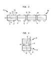
- FIG. 2is a cross-sectional view of a plurality of subassemblies attached to one another to form a stacked assembly;
- FIG. 3is a cross-sectional view of the stacked assembly of FIG. 2 after the stacked assembly has been diced into individual units;
- FIG. 4is a cross-sectional view of individual units of FIG. 3 stacked upon each other.
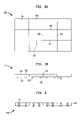
- FIG. 5Ais a top view of a subassembly according to one embodiment of the present invention.
- FIG. 5Bis a cross-sectional view of the subassembly of FIG. 5A ;
- FIG. 6is a cross-sectional view of the subassembly of FIG. 5B at a later stage of assembly;
- FIG. 7is a cross-sectional view of a plurality of subassemblies of FIG. 6 attached to one another to form a stacked assembly;
- FIG. 8is a cross-sectional view of the stacked assembly of FIG. 7 after the stacked assembly has been diced into individual units;
- FIG. 9is a cross-sectional view of individual units of FIG. 8 stacked upon each other.
- FIGS. 1A and 1Billustrate a top view and a cross-sectional view, respectively of a wafer or first subassembly 10 .
- a portion of a first wafer or subassembly 10includes a plurality of microelectronic elements 12 , each positioned side by side and adjacent to one another.
- the first subassemblypreferably includes numerous rows of microelectronic elements 12 aligned along an X-axis and a Y-axis in various columns and rows.
- the microelectronic elements 12are formed integral with one another using conventional semiconductor process techniques.
- the present inventionis also applicable to reconstituted wafers.
- Each microelectronic element 12includes a front face 14 and an oppositely-facing rear face 16 .
- the microelectronic elements 12also include first edges 18 , second edges 20 , third edges 19 and fourth edges 21 , all of which extend from the front faces 14 to the rear faces 16 of the microelectronic elements 12 .
- a first edge 18 of one microelectronic element 12is attached to a second edge 20 of a second and adjacent microelectronic element 12 .
- the microelectronic elements 12 positioned within the middle of the first subassembly 10are bordered by an adjacent microelectronic element 12 at all four edges, as shown in FIG. 1A .
- the microelectronic elements 12 positioned at a first end 11 , a second end 13 , a third end 15 or a fourth end 17 of the waferhave at least one edge unencumbered by an additional microelectronic element.
- first wafer/subassembly 10may include any number of microelectronic elements including as little as one or as many as is desirable.
- Each of the microelectronic elements 12 in subassembly 10also include a plurality of contacts 22 exposed at their respective front faces 16 . Further, the contacts 22 are attached to traces 24 that extend from the contacts 22 to an edge of the microelectronic element.
- microelectronic 12 ′includes contact 22 ′ and trace 24 ′, which extends from contact 22 ′ to first edge 18 ′ of the microelectronic element 12 ′.
- microelectronic element 12 ′′includes contact 22 ′′ and trace 24 ′′, which extends from contact 22 ′′ to second edge 20 ′′ of microelectronic element 12 ′′.
- traces 24 ′ and 24 ′′actually are a unitary structure extending between contacts 22 ′ and 22 ′′ of adjacent microelectronic elements 12 ′, 12 ′′.
- traces 24 ′ and 24 ′′meet at the attachment point of microelectronic elements 12 ′ and 12 ′′, or at saw lane 23 ′.
- the first subassembly 10is positioned under a second wafer/subassembly 10 A.
- the second subassembly 10 Ais similarly constructed to the first subassembly 10 , and thus like elements will be given similar character references unless otherwise specified.
- the second assembly 10 Ais inverted such that contacts 22 A exposed at front faces 14 A of microelectronic elements 12 A face in an opposite direction as opposed to contacts 22 of subassembly 10 .
- the rear faces 16 A of subassembly 10 Aface towards the rear faces 16 of subassembly 10 .
- the microelectronic elements 12are aligned with the microelectronic elements 12 A.
- the respective first, second, third, and fourth edges of each of the microelectronic elements 12 , 12 Aare aligned along respective longitudinal axes.
- the stacked assembly 30consists of a plurality of microelectronic elements 12 , 12 A, oriented and aligned in various rows and columns.
- an adhesive layer 32is positioned between the rear faces 16 , 16 A and adhered thereto.
- the adhesive layer 32is preferably comprised of an adhesive, epoxy or the like, and once cured, maintains a connection between the two subassemblies 10 , 10 A, such that the subassemblies are attached to one another and form stacked assembly 30 .
- the two subassemblies 10 , 10 Amay be attached using other methods that do not involve the use of an adhesive such as directly attaching the rear faces 16 of the subassembly 10 to the rear faces 16 A of the second subassembly 10 A. For example, solder bonding, eutectic bonding, diffusion bonding or other known bonding procedures can be used.
- the stacked assembly 30is diced to form individual stacked units 34 using a mechanical cutting instrument not shown in the figures. Examples of such a mechanical cutting instrument can be found in U.S. Pat. Nos. 6,646,289 and 6,972,480, the disclosures of which are hereby incorporated by reference herein.
- the stacked assembly 30is diced at locations that correspond to saw lanes 23 , 23 A of the individual subassemblies 10 , 10 A and various edges of the microelectronic elements 12 , 12 A. Since the ends of the traces 24 , 24 A that are remote from the contacts 22 , 22 A are positioned within the saw lanes 23 , 23 A, the dicing of the stacked assembly 30 causes these ends to become exposed.
- Each individual stacked unit 34includes a microelectronic element 12 A disposed above a microelectronic element 12 and attached thereto by adhesive layer 32 .
- the respective front faces 14 , 14 A of the microelectronic elements 12 , 12 Aface in opposite directions as do the contacts 22 , 22 A of respective microelectronic elements.
- the individual stacked units 34include a first side wall 36 and a second side wall 38 that extend between the front faces 14 , 14 A of the microelectronic elements 12 and 12 A. Adjacent to both side walls 36 , 38 are the ends of the traces 24 , 24 A that are exposed after the dicing process.
- a trace bridge 40extends from a trace 40 across either side wall 36 or side wall 38 to a trace 24 A, and thereby electrically interconnects the two traces disposed on opposite faces of individual stacked units 34 .
- the traces bridgesextend about the edges of the microelectronic elements as well as the edges of the adhesive layer 32 that is exposed as a result of the dicing process.
- a contact 22is in electrical communication with a contact 22 A.
- a dielectric layer 41may be disposed onto the exposed edges of the microelectronic elements and adhesive layer so as to electrically isolate the trace bridges from the bodies of the microelectronic elements if desired.
- a mass of conductive material 42may be deposited onto contacts 22 so as to enable the individual stacked units 34 to be electrically connected to a substrate such as a circuit panel and the like.
- the mass of conductive material 42may be a ball of solder or similar material.
- individual stacked units 34 and 34 ′may be stacked one upon another with contacts of individual stacked unit 34 being electrically connected to contacts of individual stacked unit 34 ′ as shown in FIG. 4 .
- the contacts 50 exposed at a lower surface 52 of stacked unit 34is aligned with the contacts 50 ′ exposed at the top surface 54 ′ of stacked unit 34 ′
- the contacts 50 and 50 ′may then be electrically connected using a mass of conductive material 56 such as solder or attached to one another using other methods known to those in the art.
- a subassembly 110 including a plurality of microelectronic elements 112may be provided as shown in FIGS. 5A and 5B .
- Subassembly 110is similarly constructed as subassembly 10 and includes many of the same features. For this reason, like elements will be given similar character references unless otherwise specified.
- the microelectronic elements 112 of subassembly 110include a front face 114 and an oppositely-facing rear face 116 .
- each microelectronic element 112includes a first edge 118 , a second edge 120 , a third edge 119 and a fourth edge 121 extending between the front face 114 and rear face 116 .
- the locationswere one edge of a first microelectronic element abuts an edge of a second microelectronic element forms saw lanes 123 .
- the saw lanesmay be cut there through without damaging the individual microelectronic elements 112 of the subassembly 110 .
- demarcation linesare shown in FIGS. 5A to 5B for clarity of illustration, in practice a clear separation between adjacent microelectronic elements 112 may not be recognizable.
- Each microelectronic element 112also includes a plurality of contacts 122 exposed at their respective front face 114 .
- the subassembly 110is illustrated having four rows and three columns of microelectronic elements, the number of microelectronic elements may be as little as one and as many as is desirable.
- the vias 130are filled with a conductive material 131 such as a metal.
- the conductive material 131may for instance be formed from copper or a copper/gold alloy.
- the saw lanes 123 of subassembly 110are aligned with the saw lanes 123 ′ of second subassembly 110 ′ and the vias 130 , 130 ′ of each of the subassemblies are also aligned.
- the vias 130 to the vias 130 ′the contacts 122 of the microelectronic elements 112 are aligned with the contacts 122 ′ of the second subassembly and the conductive material 131 , 131 ′ of each of the vias 130 , 130 ′ are brought proximate to one another.
- a second conductive material 137may be utilized.
- masses of the second conductive material 137such as solder, are disposed in and around the vias 130 proximate the rear faces 116 of the microelectronic elements 112 and in contact with the conductive material 131 contained within the vias.
- the subassembly 110is then brought proximate with the second subassembly 110 ′ such that the second conductive material 137 is proximate vias 130 ′ and in contact with the conductive material 131 ′ of the second subassembly. As shown in FIG.
- this configurationcauses the contacts 122 to be electrically connected to contacts 122 ′ through the various conductive materials disposed within the vias 130 , 130 ′ and thus the conductive material 131 , 131 ′ act as electrical bridges between contacts 122 , 122 ′.
- a back fillsuch as encapsulant material 134 or an adhesive may be positioned between the two subassemblies 110 , 110 ′ to provide additional rigidity to the stacked assembly 132 .
- the conductive material 131 of subassembly 110may be directly adhered to the conductive material 131 ′ of the second subassembly 110 ′.
- the conductive material 130 , 130 ′is copper
- the copper in each via 130 , 130 ′is reflowed and allowed to contact the copper in an aligned via.
- the copper in adjacent vias 130 , 130 ′forms, not only an attachment area between the subassemblies but also an electrical connection between contacts 122 , 122 ′.
- the stacked assembly 132is now ready to be diced into individual stacked units 140 .
- a similar mechanical instrument(not shown in the figures) described previously is brought proximate the saw lanes 123 , 123 ′ of each of the subassemblies 110 , 110 ′.
- the mechanical toolis passed through the stacked assembly 132 at positions that correspond to the saw lanes 123 , 123 ′ thereby dissecting the stacked assembly into individual stacked units 140 .
- a mass of solder 142 or other conductive materialmay be disposed on exposed contacts 122 or 122 ′ so as to enable the individual stacked units 140 to be attached to a substrate such as a circuit panel.
- the stacked assembly 132may also be attached to a circuit panel without having to dice the assembly into individual units if desired.
- individual stacked units 140 and 140 ′may be stacked one upon another with the contacts of individual stacked unit 140 being electrically connected to contacts of individual stacked unit 140 ′.
- the contacts 150 exposed at a lower surface 152 of stacked unit 140are aligned with the contacts 150 ′ exposed at the top surface 154 ′ of stacked unit 140 ′
- the contacts 150 and 150 ′may then be electrically connected using a mass of conductive material 156 such as solder or attached to one another using other methods known to those in the art.
- the entire assembly 160may be attached to a substrate such as circuit panel 170 illustrated in FIG. 9 , which includes conductive pads 172 .
Landscapes
- Engineering & Computer Science (AREA)
- Microelectronics & Electronic Packaging (AREA)
- Power Engineering (AREA)
- Computer Hardware Design (AREA)
- Physics & Mathematics (AREA)
- Condensed Matter Physics & Semiconductors (AREA)
- General Physics & Mathematics (AREA)
- Wire Bonding (AREA)
- Dicing (AREA)
- Cooling Or The Like Of Semiconductors Or Solid State Devices (AREA)
Abstract
Description
- The present invention generally relates to stacked microelectronic packages and more particularly relates to stacked microelectronic packages fabricated at the wafer level and to methods of making such packages.
- Semiconductor chips are flat bodies with contacts disposed on the front surface that are connected to the internal electrical circuitry of the chip itself. Semiconductor chips are typically packaged with substrates to form microelectronic packages having terminals that are electrically connected to the chip contacts. The package may then be connected to test equipment to determine whether the packaged device conforms to a desired performance standard. Once tested, the package may be connected to a larger circuit, e.g., a circuit in an electronic product such as a computer or a cell phone.
- The substrate materials used for packaging semiconductor chips are selected for their compatibility with the processes used to form the packages. For example, during solder or other bonding operations, intense heat may be applied to the substrate. Accordingly, metal lead frames have been used as substrates. Laminate substrates have also been used to package microelectronic devices. Such substrates may include two to four alternating layers of fiberglass and epoxy, wherein successive fiberglass layers may be laid in traversing, e.g., orthogonal, directions. Optionally, heat resistive compounds such as bismaleimide triazine (BT) may be added to such laminate substrates.
- Tapes have been used as substrates to provide thinner microelectronic packages. Such tapes are typically provided in the form of sheets or rolls of sheets. For example, single and double sided sheets of copper-on-polyimide are commonly used. Polyimide based films offer good thermal and chemical stability and a low dielectric constant, while copper having high tensile strength, ductility, and flexure has been advantageously used in both flexible circuit and chip scale packaging applications. However, such tapes are relatively expensive, particularly as compared to lead frames and laminate substrates.
- Microelectronic packages also include wafer level packages, which provide a package for a semiconductor component that is fabricated while the die are still in a wafer form. The wafer is subject to a number of additional process steps to form the package structure and the wafer is then diced to free the individual die, with no additional fabrication steps being necessary. Wafer level processing provides an advantage in that the cost of the packaging processes are divided among the various die on the wafer, resulting in a very low price differential between the die and the component. Furthermore, the package footprint can be substantially similar to the die size, resulting in very efficient utilization of area on a printed circuit board (PCB) to which the die will eventually be attached. As a result of these features, die packaged in this manner are commonly referred to as wafer level chip scale package (WLCSP).
- In order to save space certain conventional designs have stacked multiple microelectronic chips within a package. This allows the package to occupy a surface area on a substrate that is less than the total surface area of the chips in the stack.
- In spite of the above advances, there remains a need for improved wafer-scale packages and especially stacked wafer-scale packages that are reliable and that are economical to manufacture.
- The present invention is directed to a microelectronic assembly that includes a first microelectronic element having a first rear surface. The assembly further includes a second microelectronic element having a second rear surface. The second microelectronic element is attached to the first microelectronic element so as to form a stacked package. The first rear surface of the first microelectronic element faces toward the second rear surface of the second microelectronic element.
- Moreover, the assembly includes at least one bridging element. The first microelectronic element and second microelectronic element each have a front surface and a plurality of contacts exposed there at. The at least one bridging element extends between the plurality of contacts of the first microelectronic element and the plurality of contacts of the second microelectronic element so as to electrically connect the two.
- In one aspect the first microelectronic element includes a first edge and a second edge extending from the front surface to the rear surface of the first microelectronic element. And the at least one bridging element is disposed outside of the first edge and second edge. A plurality of traces exposed on the respective front surfaces of the first microelectronic element and second microelectronic element may be included as well. At least some of the plurality of traces extend from at least some of the plurality of contacts on the first microelectronic element to the at least one bridging element and at least some of the plurality of traces extend from at least some of the plurality of contacts of the second microelectronic element to the at least one bridging element.
- The microelectronic assembly in certain embodiments includes an adhesive that attaches the first microelectronic element to the second microelectronic element. And in another aspect, the first microelectronic element includes a first edge and a second edge. The at least one bridging element is positioned between the first edge and the second edge. Also the second microelectronic element may have a first edge and a second edge such that the at least one bridging element is positioned between the first edge and the second edge of the second microelectronic element.
- In another aspect, the first microelectronic element includes a plurality of vias extending from the front face to the rear face and the at least one bridging element is disposed within at least one of the plurality of vias.
- The assembly may further include a third microelectronic element having a front face and a rear face and a fourth microelectronic element having a rear face. The third and fourth microelectronic elements are attached such that the rear face of the third microelectronic element faces toward the rear face of the fourth microelectronic element. The third microelectronic element is also attached to the first second microelectronic element such that the front face of the third microelectronic element faces toward the front surface of the second microelectronic element.
- The present invention is also directed to a method of assembling a stacked microelectronic assembly comprising the steps of forming a microelectronic assembly by stacking a first subassembly including a plurality of microelectronic elements onto a second subassembly including a plurality of microelectronic elements. The rear faces of the first subassembly and second subassembly confront one another. Next, a plurality of contacts exposed at a front face of the first subassembly is connected to a plurality of contacts exposed at a front face of the second subassembly.
- The first subassembly and second subassembly each may include saw lanes that are aligned during the step of forming the microelectronic assembly. And the method may include dicing through the saw lanes of the first and second subassemblies so as so form individual stacked units. At least some of the plurality of microelectronic elements of the first subassembly and the second subassembly have traces that extend from respective contacts to the saw lanes of the respective first and second subassemblies such that after the dicing step the traces are exposed.
FIG. 1A is a top view of a subassembly according to one embodiment of the present invention;FIG. 1B is a cross-sectional view of the subassembly ofFIG. 1A ;FIG. 2 is a cross-sectional view of a plurality of subassemblies attached to one another to form a stacked assembly;FIG. 3 is a cross-sectional view of the stacked assembly ofFIG. 2 after the stacked assembly has been diced into individual units;FIG. 4 is a cross-sectional view of individual units ofFIG. 3 stacked upon each other.FIG. 5A is a top view of a subassembly according to one embodiment of the present invention;FIG. 5B is a cross-sectional view of the subassembly ofFIG. 5A ;FIG. 6 is a cross-sectional view of the subassembly ofFIG. 5B at a later stage of assembly;FIG. 7 is a cross-sectional view of a plurality of subassemblies ofFIG. 6 attached to one another to form a stacked assembly;FIG. 8 is a cross-sectional view of the stacked assembly ofFIG. 7 after the stacked assembly has been diced into individual units; andFIG. 9 is a cross-sectional view of individual units ofFIG. 8 stacked upon each other.- Reference is now made to
FIGS. 1A and 1B , which illustrate a top view and a cross-sectional view, respectively of a wafer orfirst subassembly 10. As shown in the figures, a portion of a first wafer orsubassembly 10 includes a plurality ofmicroelectronic elements 12, each positioned side by side and adjacent to one another. The first subassembly preferably includes numerous rows ofmicroelectronic elements 12 aligned along an X-axis and a Y-axis in various columns and rows. Themicroelectronic elements 12 are formed integral with one another using conventional semiconductor process techniques. The present invention is also applicable to reconstituted wafers. - Each
microelectronic element 12 includes afront face 14 and an oppositely-facingrear face 16. Themicroelectronic elements 12 also includefirst edges 18, second edges20, third edges19 andfourth edges 21, all of which extend from the front faces14 to the rear faces16 of themicroelectronic elements 12. As shown inFIGS. 1A and 1B , afirst edge 18 of onemicroelectronic element 12 is attached to asecond edge 20 of a second and adjacentmicroelectronic element 12. Thus, themicroelectronic elements 12 positioned within the middle of thefirst subassembly 10 are bordered by an adjacentmicroelectronic element 12 at all four edges, as shown inFIG. 1A . Themicroelectronic elements 12 positioned at afirst end 11, asecond end 13, athird end 15 or afourth end 17 of the wafer have at least one edge unencumbered by an additional microelectronic element. - Although the edges are depicted in the drawings for clarity of illustration, in practice the edges may not be visible. Rather, at this stage the edges or strips where adjacent
microelectronic elements 12 contact one another are saw lanes or strips where the wafer can be cut without damaging the individual microelectronic elements. For instance, as shown inFIG. 1B ,second edge 20′ ofmicroelectronic element 12′ abutsfirst edge 18″ ofmicroelectronic element 12″ and forms asaw lane 23. Similarly, throughout thewafer 10, sawlanes 23 are located at positions wheremicroelectronic elements 12 abut one another. The first wafer/subassembly 10 may include any number of microelectronic elements including as little as one or as many as is desirable. - Each of the
microelectronic elements 12 insubassembly 10 also include a plurality ofcontacts 22 exposed at their respective front faces16. Further, thecontacts 22 are attached totraces 24 that extend from thecontacts 22 to an edge of the microelectronic element. For instance, microelectronic12′ includescontact 22′ and trace24′, which extends fromcontact 22′ tofirst edge 18′ of themicroelectronic element 12′. Similarly,microelectronic element 12″ includescontact 22″ and trace24″, which extends fromcontact 22″ tosecond edge 20″ ofmicroelectronic element 12″. In one embodiment, traces24′ and24″ actually are a unitary structure extending betweencontacts 22′ and22″ of adjacentmicroelectronic elements 12′,12″. Thus, traces24′ and24″ meet at the attachment point ofmicroelectronic elements 12′ and12″, or atsaw lane 23′. However, it is not required that the traces actually contact one another but rather that thesetraces 24 simply extend toward a respective end of themicroelectronic elements 12 and into the width of the saw lanes. - As shown in
FIG. 2 , to create astacked assembly 30, thefirst subassembly 10 is positioned under a second wafer/subassembly10A. The second subassembly10A is similarly constructed to thefirst subassembly 10, and thus like elements will be given similar character references unless otherwise specified. - As shown in
FIG. 2 , the second assembly10A is inverted such that contacts22A exposed at front faces14A of microelectronic elements12A face in an opposite direction as opposed tocontacts 22 ofsubassembly 10. Thus, as shown inFIG. 2 , the rear faces16A of subassembly10A face towards the rear faces16 ofsubassembly 10. When positioning therespective subassemblies 10,10A, themicroelectronic elements 12 are aligned with the microelectronic elements12A. The respective first, second, third, and fourth edges of each of themicroelectronic elements 12,12A are aligned along respective longitudinal axes. And the respective sawlanes 23,23A of each of thesubassemblies 10,10A are also aligned. The stackedassembly 30 consists of a plurality ofmicroelectronic elements 12,12A, oriented and aligned in various rows and columns. - To attach the two
subassemblies adhesive layer 32 is positioned between the rear faces16,16A and adhered thereto. Theadhesive layer 32 is preferably comprised of an adhesive, epoxy or the like, and once cured, maintains a connection between the twosubassemblies 10,10A, such that the subassemblies are attached to one another and form stackedassembly 30. The twosubassemblies 10,10A may be attached using other methods that do not involve the use of an adhesive such as directly attaching the rear faces16 of thesubassembly 10 to the rear faces16A of the second subassembly10A. For example, solder bonding, eutectic bonding, diffusion bonding or other known bonding procedures can be used. - Next, the stacked
assembly 30 is diced to form individualstacked units 34 using a mechanical cutting instrument not shown in the figures. Examples of such a mechanical cutting instrument can be found in U.S. Pat. Nos. 6,646,289 and 6,972,480, the disclosures of which are hereby incorporated by reference herein. The stackedassembly 30 is diced at locations that correspond to sawlanes 23,23A of theindividual subassemblies 10,10A and various edges of themicroelectronic elements 12,12A. Since the ends of thetraces 24,24A that are remote from thecontacts 22,22A are positioned within thesaw lanes 23,23A, the dicing of the stackedassembly 30 causes these ends to become exposed. - Each individual
stacked unit 34 includes a microelectronic element12A disposed above amicroelectronic element 12 and attached thereto byadhesive layer 32. The respective front faces14,14A of themicroelectronic elements 12,12A face in opposite directions as do thecontacts 22,22A of respective microelectronic elements. In addition, the individualstacked units 34 include afirst side wall 36 and asecond side wall 38 that extend between the front faces14,14A of themicroelectronic elements 12 and12A. Adjacent to bothside walls traces 24,24A that are exposed after the dicing process. - Bridging elements such as trace bridges40 are then formed on the
side walls trace bridge 40 extends from atrace 40 across eitherside wall 36 orside wall 38 to a trace24A, and thereby electrically interconnects the two traces disposed on opposite faces of individual stackedunits 34. The traces bridges extend about the edges of the microelectronic elements as well as the edges of theadhesive layer 32 that is exposed as a result of the dicing process. As a result of thetrace bridge 40, acontact 22 is in electrical communication with a contact22A. Prior to the trace bridges40 being formed, a dielectric layer41 may be disposed onto the exposed edges of the microelectronic elements and adhesive layer so as to electrically isolate the trace bridges from the bodies of the microelectronic elements if desired. - With reference still to
FIG. 3 , a mass ofconductive material 42 may be deposited ontocontacts 22 so as to enable the individualstacked units 34 to be electrically connected to a substrate such as a circuit panel and the like. The mass ofconductive material 42 may be a ball of solder or similar material. - According to one aspect of the present invention, individual
stacked units unit 34 being electrically connected to contacts of individual stackedunit 34′ as shown inFIG. 4 . For example, to electrically connect the individualstacked units contacts 50 exposed at alower surface 52 of stackedunit 34 is aligned with thecontacts 50′ exposed at thetop surface 54′ of stackedunit 34′ Thecontacts conductive material 56 such as solder or attached to one another using other methods known to those in the art. - In one aspect of the present invention, a
subassembly 110 including a plurality ofmicroelectronic elements 112 may be provided as shown inFIGS. 5A and 5B .Subassembly 110 is similarly constructed assubassembly 10 and includes many of the same features. For this reason, like elements will be given similar character references unless otherwise specified. Themicroelectronic elements 112 ofsubassembly 110 include afront face 114 and an oppositely-facingrear face 116. - Additionally, each
microelectronic element 112 includes afirst edge 118, asecond edge 120, athird edge 119 and afourth edge 121 extending between thefront face 114 andrear face 116. The locations were one edge of a first microelectronic element abuts an edge of a second microelectronic element forms sawlanes 123. As mentioned with regard tosubassembly 10, the saw lanes may be cut there through without damaging the individualmicroelectronic elements 112 of thesubassembly 110. And although demarcation lines are shown inFIGS. 5A to 5B for clarity of illustration, in practice a clear separation between adjacentmicroelectronic elements 112 may not be recognizable. Eachmicroelectronic element 112 also includes a plurality ofcontacts 122 exposed at their respectivefront face 114. Although thesubassembly 110 is illustrated having four rows and three columns of microelectronic elements, the number of microelectronic elements may be as little as one and as many as is desirable. - Next, with reference to
FIG. 6 , thesubassembly 110 is subjected to a mechanical cutting process that bores vias130 through each of themicroelectronic elements 112. The vias extend from arear face 116 to afront face 114 of each of the microelectronic elements. And each of thevias 130 is preferably aligned with acontact 122 exposed on thefront face 114 of each of themicroelectronic elements 112 such that thecontacts 122 are not only exposed at the front faces114 but also at the rear faces116. - After the
vias 130 are formed, they are filled with aconductive material 131 such as a metal. Theconductive material 131 may for instance be formed from copper or a copper/gold alloy. - As shown in
FIG. 7 , astacked assembly 132 may be assembled by attaching thefirst subassembly 110 to asecond subassembly 110′. Thesecond subassembly 110′ is similarly constructed assubassembly 110 and like features are described using similar character references unless otherwise specified. To formstacked assembly 132, thesecond subassembly 110′ is inverted such that the rear faces116′ of themicroelectronic elements 112′ of the second subassembly face toward the rear faces116 ofmicroelectronic elements 112. When aligning the two subassemblies, thesaw lanes 123 ofsubassembly 110 are aligned with thesaw lanes 123′ ofsecond subassembly 110′ and thevias vias 130 to thevias 130′, thecontacts 122 of themicroelectronic elements 112 are aligned with thecontacts 122′ of the second subassembly and theconductive material vias - To attach the
second subassembly 110′ to thesubassembly 110, a secondconductive material 137 may be utilized. For example, masses of the secondconductive material 137, such as solder, are disposed in and around thevias 130 proximate the rear faces116 of themicroelectronic elements 112 and in contact with theconductive material 131 contained within the vias. Thesubassembly 110 is then brought proximate with thesecond subassembly 110′ such that the secondconductive material 137 isproximate vias 130′ and in contact with theconductive material 131′ of the second subassembly. As shown inFIG. 7 , this configuration causes thecontacts 122 to be electrically connected tocontacts 122′ through the various conductive materials disposed within thevias conductive material contacts encapsulant material 134 or an adhesive may be positioned between the twosubassemblies stacked assembly 132. - In an alternate embodiment, although not shown in the figures, the
conductive material 131 ofsubassembly 110 may be directly adhered to theconductive material 131′ of thesecond subassembly 110′. For instance, if theconductive material adjacent vias contacts - The
stacked assembly 132 is now ready to be diced into individualstacked units 140. For this, a similar mechanical instrument (not shown in the figures) described previously is brought proximate thesaw lanes subassemblies stacked assembly 132 at positions that correspond to thesaw lanes stacked units 140. Of course, if thestacked assembly 132 was created with subassemblies that only included single microelectronic elements a dissection step is not required. A mass ofsolder 142 or other conductive material may be disposed on exposedcontacts stacked units 140 to be attached to a substrate such as a circuit panel. - The
stacked assembly 132 may also be attached to a circuit panel without having to dice the assembly into individual units if desired. - According to one aspect of the present invention, individual
stacked units stacked unit 140 being electrically connected to contacts of individualstacked unit 140′. For example, to electrically connect the individualstacked units contacts 150 exposed at alower surface 152 ofstacked unit 140 are aligned with thecontacts 150′ exposed at thetop surface 154′ ofstacked unit 140′ Thecontacts conductive material 156 such as solder or attached to one another using other methods known to those in the art. Theentire assembly 160 may be attached to a substrate such ascircuit panel 170 illustrated inFIG. 9 , which includesconductive pads 172. - Although the invention herein has been described with reference to particular embodiments, it is to be understood that these embodiments are merely illustrative of the principles and applications of the present invention. It is therefore to be understood that numerous modifications may be made to the illustrative embodiments and that other arrangements may be devised without departing from the spirit and scope of the present invention as defined by the appended claims.
Claims (19)
Priority Applications (7)
| Application Number | Priority Date | Filing Date | Title |
|---|---|---|---|
| US11/648,172US7952195B2 (en) | 2006-12-28 | 2006-12-28 | Stacked packages with bridging traces |
| KR1020097015570AKR101454332B1 (en) | 2006-12-28 | 2007-12-20 | Stacked packages |
| JP2009544043AJP5567346B2 (en) | 2006-12-28 | 2007-12-20 | Stacked package |
| PCT/US2007/026095WO2008085391A2 (en) | 2006-12-28 | 2007-12-20 | Stacked packages |
| EP07867901.6AEP2097925B1 (en) | 2006-12-28 | 2007-12-20 | Stacked packages |
| CN2007800504745ACN101595562B (en) | 2006-12-28 | 2007-12-20 | Stacked packages |
| US13/115,318US8349654B2 (en) | 2006-12-28 | 2011-05-25 | Method of fabricating stacked packages with bridging traces |
Applications Claiming Priority (1)
| Application Number | Priority Date | Filing Date | Title |
|---|---|---|---|
| US11/648,172US7952195B2 (en) | 2006-12-28 | 2006-12-28 | Stacked packages with bridging traces |
Related Child Applications (1)
| Application Number | Title | Priority Date | Filing Date |
|---|---|---|---|
| US13/115,318DivisionUS8349654B2 (en) | 2006-12-28 | 2011-05-25 | Method of fabricating stacked packages with bridging traces |
Publications (2)
| Publication Number | Publication Date |
|---|---|
| US20080157323A1true US20080157323A1 (en) | 2008-07-03 |
| US7952195B2 US7952195B2 (en) | 2011-05-31 |
Family
ID=39488194
Family Applications (2)
| Application Number | Title | Priority Date | Filing Date |
|---|---|---|---|
| US11/648,172Active2028-08-23US7952195B2 (en) | 2006-12-28 | 2006-12-28 | Stacked packages with bridging traces |
| US13/115,318ActiveUS8349654B2 (en) | 2006-12-28 | 2011-05-25 | Method of fabricating stacked packages with bridging traces |
Family Applications After (1)
| Application Number | Title | Priority Date | Filing Date |
|---|---|---|---|
| US13/115,318ActiveUS8349654B2 (en) | 2006-12-28 | 2011-05-25 | Method of fabricating stacked packages with bridging traces |
Country Status (6)
| Country | Link |
|---|---|
| US (2) | US7952195B2 (en) |
| EP (1) | EP2097925B1 (en) |
| JP (1) | JP5567346B2 (en) |
| KR (1) | KR101454332B1 (en) |
| CN (1) | CN101595562B (en) |
| WO (1) | WO2008085391A2 (en) |
Cited By (3)
| Publication number | Priority date | Publication date | Assignee | Title |
|---|---|---|---|---|
| WO2014033099A2 (en) | 2012-08-27 | 2014-03-06 | Digital Optics Corporation Europe Limited | Rearview imaging systems for vehicle |
| US9001268B2 (en) | 2012-08-10 | 2015-04-07 | Nan Chang O-Film Optoelectronics Technology Ltd | Auto-focus camera module with flexible printed circuit extension |
| US9007520B2 (en) | 2012-08-10 | 2015-04-14 | Nanchang O-Film Optoelectronics Technology Ltd | Camera module with EMI shield |
Families Citing this family (34)
| Publication number | Priority date | Publication date | Assignee | Title |
|---|---|---|---|---|
| US7901989B2 (en) | 2006-10-10 | 2011-03-08 | Tessera, Inc. | Reconstituted wafer level stacking |
| US8513789B2 (en) | 2006-10-10 | 2013-08-20 | Tessera, Inc. | Edge connect wafer level stacking with leads extending along edges |
| US7829438B2 (en) | 2006-10-10 | 2010-11-09 | Tessera, Inc. | Edge connect wafer level stacking |
| US7759166B2 (en)* | 2006-10-17 | 2010-07-20 | Tessera, Inc. | Microelectronic packages fabricated at the wafer level and methods therefor |
| US7952195B2 (en)* | 2006-12-28 | 2011-05-31 | Tessera, Inc. | Stacked packages with bridging traces |
| US8723332B2 (en)* | 2007-06-11 | 2014-05-13 | Invensas Corporation | Electrically interconnected stacked die assemblies |
| JP5572089B2 (en) | 2007-07-27 | 2014-08-13 | テッセラ,インコーポレイテッド | Reconfigured wafer stack packaging with pad extension after application |
| US8551815B2 (en) | 2007-08-03 | 2013-10-08 | Tessera, Inc. | Stack packages using reconstituted wafers |
| US8043895B2 (en) | 2007-08-09 | 2011-10-25 | Tessera, Inc. | Method of fabricating stacked assembly including plurality of stacked microelectronic elements |
| WO2009035849A2 (en) | 2007-09-10 | 2009-03-19 | Vertical Circuits, Inc. | Semiconductor die mount by conformal die coating |
| CN101999167B (en) | 2008-03-12 | 2013-07-17 | 伊文萨思公司 | Support mounted electrically interconnected die assembly |
| US7863159B2 (en) | 2008-06-19 | 2011-01-04 | Vertical Circuits, Inc. | Semiconductor die separation method |
| US9153517B2 (en) | 2008-05-20 | 2015-10-06 | Invensas Corporation | Electrical connector between die pad and z-interconnect for stacked die assemblies |
| JP5639052B2 (en) | 2008-06-16 | 2014-12-10 | テッセラ,インコーポレイテッド | Edge stacking at wafer level |
| WO2010104610A2 (en) | 2009-03-13 | 2010-09-16 | Tessera Technologies Hungary Kft. | Stacked microelectronic assemblies having vias extending through bond pads |
| WO2010151578A2 (en) | 2009-06-26 | 2010-12-29 | Vertical Circuits, Inc. | Electrical interconnect for die stacked in zig-zag configuration |
| JP5425584B2 (en)* | 2009-10-15 | 2014-02-26 | ルネサスエレクトロニクス株式会社 | Manufacturing method of semiconductor device |
| WO2011056668A2 (en) | 2009-10-27 | 2011-05-12 | Vertical Circuits, Inc. | Selective die electrical insulation additive process |
| US7915083B1 (en)* | 2009-10-28 | 2011-03-29 | Headway Technologies, Inc. | Method of manufacturing layered chip package |
| TWI544604B (en) | 2009-11-04 | 2016-08-01 | 英維瑟斯公司 | Stacked die assembly having reduced stress electrical interconnects |
| US8541887B2 (en) | 2010-09-03 | 2013-09-24 | Headway Technologies, Inc. | Layered chip package and method of manufacturing same |
| US8441112B2 (en)* | 2010-10-01 | 2013-05-14 | Headway Technologies, Inc. | Method of manufacturing layered chip package |
| US8618646B2 (en)* | 2010-10-12 | 2013-12-31 | Headway Technologies, Inc. | Layered chip package and method of manufacturing same |
| US8652877B2 (en) | 2010-12-06 | 2014-02-18 | Headway Technologies, Inc. | Method of manufacturing layered chip package |
| US8653639B2 (en)* | 2011-06-09 | 2014-02-18 | Headway Technologies, Inc. | Layered chip package and method of manufacturing same |
| KR102190382B1 (en)* | 2012-12-20 | 2020-12-11 | 삼성전자주식회사 | Semiconductor package |
| US9241400B2 (en) | 2013-08-23 | 2016-01-19 | Seagate Technology Llc | Windowed reference planes for embedded conductors |
| US9825002B2 (en) | 2015-07-17 | 2017-11-21 | Invensas Corporation | Flipped die stack |
| US9490195B1 (en) | 2015-07-17 | 2016-11-08 | Invensas Corporation | Wafer-level flipped die stacks with leadframes or metal foil interconnects |
| US9871019B2 (en) | 2015-07-17 | 2018-01-16 | Invensas Corporation | Flipped die stack assemblies with leadframe interconnects |
| US9508691B1 (en) | 2015-12-16 | 2016-11-29 | Invensas Corporation | Flipped die stacks with multiple rows of leadframe interconnects |
| US10566310B2 (en) | 2016-04-11 | 2020-02-18 | Invensas Corporation | Microelectronic packages having stacked die and wire bond interconnects |
| US9595511B1 (en) | 2016-05-12 | 2017-03-14 | Invensas Corporation | Microelectronic packages and assemblies with improved flyby signaling operation |
| US9728524B1 (en) | 2016-06-30 | 2017-08-08 | Invensas Corporation | Enhanced density assembly having microelectronic packages mounted at substantial angle to board |
Citations (90)
| Publication number | Priority date | Publication date | Assignee | Title |
|---|---|---|---|---|
| US4074342A (en)* | 1974-12-20 | 1978-02-14 | International Business Machines Corporation | Electrical package for lsi devices and assembly process therefor |
| US4500905A (en)* | 1981-09-30 | 1985-02-19 | Tokyo Shibaura Denki Kabushiki Kaisha | Stacked semiconductor device with sloping sides |
| US4765864A (en)* | 1987-07-15 | 1988-08-23 | Sri International | Etching method for producing an electrochemical cell in a crystalline substrate |
| US4842699A (en)* | 1988-05-10 | 1989-06-27 | Avantek, Inc. | Method of selective via-hole and heat sink plating using a metal mask |
| US4897708A (en)* | 1986-07-17 | 1990-01-30 | Laser Dynamics, Inc. | Semiconductor wafer array |
| US4954875A (en)* | 1986-07-17 | 1990-09-04 | Laser Dynamics, Inc. | Semiconductor wafer array with electrically conductive compliant material |
| US5322816A (en)* | 1993-01-19 | 1994-06-21 | Hughes Aircraft Company | Method for forming deep conductive feedthroughs |
| US5343071A (en)* | 1993-04-28 | 1994-08-30 | Raytheon Company | Semiconductor structures having dual surface via holes |
| US5412539A (en)* | 1993-10-18 | 1995-05-02 | Hughes Aircraft Company | Multichip module with a mandrel-produced interconnecting decal |
| US5424245A (en)* | 1994-01-04 | 1995-06-13 | Motorola, Inc. | Method of forming vias through two-sided substrate |
| US5426072A (en)* | 1993-01-21 | 1995-06-20 | Hughes Aircraft Company | Process of manufacturing a three dimensional integrated circuit from stacked SOI wafers using a temporary silicon substrate |
| US5466634A (en)* | 1994-12-20 | 1995-11-14 | International Business Machines Corporation | Electronic modules with interconnected surface metallization layers and fabrication methods therefore |
| US5563084A (en)* | 1994-09-22 | 1996-10-08 | Fraunhofer-Gesellschaft zur F orderung der angewandten Forschung e.V. | Method of making a three-dimensional integrated circuit |
| US5571754A (en)* | 1995-07-26 | 1996-11-05 | International Business Machines Corporation | Method of fabrication of endcap chip with conductive, monolithic L-connect for multichip stack |
| US5604673A (en)* | 1995-06-07 | 1997-02-18 | Hughes Electronics | Low temperature co-fired ceramic substrates for power converters |
| US5608264A (en)* | 1995-06-05 | 1997-03-04 | Harris Corporation | Surface mountable integrated circuit with conductive vias |
| US5614766A (en)* | 1991-09-30 | 1997-03-25 | Rohm Co., Ltd. | Semiconductor device with stacked alternate-facing chips |
| US5618752A (en)* | 1995-06-05 | 1997-04-08 | Harris Corporation | Method of fabrication of surface mountable integrated circuits |
| US5646067A (en)* | 1995-06-05 | 1997-07-08 | Harris Corporation | Method of bonding wafers having vias including conductive material |
| US5661087A (en)* | 1994-06-23 | 1997-08-26 | Cubic Memory, Inc. | Vertical interconnect process for silicon segments |
| US5682062A (en)* | 1995-06-05 | 1997-10-28 | Harris Corporation | System for interconnecting stacked integrated circuits |
| US5716759A (en)* | 1993-09-02 | 1998-02-10 | Shellcase Ltd. | Method and apparatus for producing integrated circuit devices |
| US5766984A (en)* | 1994-09-22 | 1998-06-16 | Fraunhofer-Gesellschaft Zur Foerderung Der Angewandten Forschung | Method of making a vertical integrated circuit |
| US5767001A (en)* | 1993-05-05 | 1998-06-16 | Siemens Aktiengesellschaft | Process for producing semiconductor components between which contact is made vertically |
| US5804004A (en)* | 1992-05-11 | 1998-09-08 | Nchip, Inc. | Stacked devices for multichip modules |
| US5814889A (en)* | 1995-06-05 | 1998-09-29 | Harris Corporation | Intergrated circuit with coaxial isolation and method |
| US5817530A (en)* | 1996-05-20 | 1998-10-06 | Micron Technology, Inc. | Use of conductive lines on the back side of wafers and dice for semiconductor interconnects |
| US5880010A (en)* | 1994-07-12 | 1999-03-09 | Sun Microsystems, Inc. | Ultrathin electronics |
| US5915167A (en)* | 1997-04-04 | 1999-06-22 | Elm Technology Corporation | Three dimensional structure memory |
| US5946545A (en)* | 1994-03-30 | 1999-08-31 | Internatinal Business Machines Corporation | Semiconductor stack structures and fabrication/sparing methods utilizing programmable spare circuit |
| US5973386A (en)* | 1996-02-16 | 1999-10-26 | Nec Corporation | Semiconductor substrate having silicon oxide layers formed between polysilicon layers |
| US6022758A (en)* | 1994-07-10 | 2000-02-08 | Shellcase Ltd. | Process for manufacturing solder leads on a semiconductor device package |
| US6031274A (en)* | 1996-10-11 | 2000-02-29 | Hamamatsu Photonics K.K. | Back irradiation type light-receiving device and method of making the same |
| US6040235A (en)* | 1994-01-17 | 2000-03-21 | Shellcase Ltd. | Methods and apparatus for producing integrated circuit devices |
| US6103552A (en)* | 1998-08-10 | 2000-08-15 | Lin; Mou-Shiung | Wafer scale packaging scheme |
| US6130823A (en)* | 1999-02-01 | 2000-10-10 | Raytheon E-Systems, Inc. | Stackable ball grid array module and method |
| US6177707B1 (en)* | 1998-03-02 | 2001-01-23 | U.S. Philips Corporation | Semiconductor device comprising a glass supporting body onto which a substrate with semiconductor elements and a metalization is attached by means of an adhesive |
| US6177721B1 (en)* | 1998-10-21 | 2001-01-23 | Hyundai Electronics Industries Co., Ltd | Chip stack-type semiconductor package and method for fabricating the same |
| US6188129B1 (en)* | 1997-03-24 | 2001-02-13 | Hyundai Electronics Industries Co., Ltd. | Stacked semiconductor chip package having external terminal pads and stackable chips having a protection layer |
| US6204562B1 (en)* | 1999-02-11 | 2001-03-20 | United Microelectronics Corp. | Wafer-level chip scale package |
| US6261865B1 (en)* | 1998-10-06 | 2001-07-17 | Micron Technology, Inc. | Multi chip semiconductor package and method of construction |
| US6277669B1 (en)* | 1999-09-15 | 2001-08-21 | Industrial Technology Research Institute | Wafer level packaging method and packages formed |
| US6340845B1 (en)* | 1999-01-22 | 2002-01-22 | Nec Corporation | Memory package implementing two-fold memory capacity and two different memory functions |
| US6344401B1 (en)* | 2000-03-09 | 2002-02-05 | Atmel Corporation | Method of forming a stacked-die integrated circuit chip package on a water level |
| US20020047199A1 (en)* | 2000-09-11 | 2002-04-25 | Shinji Ohuchi | Semiconductor device, manufacturing method of semiconductor device, stack type semiconductor device, and manufacturing method of stack type semiconductor device |
| US6396710B1 (en)* | 2000-05-12 | 2002-05-28 | Raytheon Company | High density interconnect module |
| US20020074637A1 (en)* | 2000-12-19 | 2002-06-20 | Intel Corporation | Stacked flip chip assemblies |
| US20020109236A1 (en)* | 2001-02-09 | 2002-08-15 | Samsung Electronics Co., Ltd. | Three-dimensional multi-chip package having chip selection pads and manufacturing method thereof |
| US20020127775A1 (en)* | 1999-12-23 | 2002-09-12 | Rambus Inc. | Redistributed bond pads in stacked integrated circuit die package |
| US20020132465A1 (en)* | 1997-04-04 | 2002-09-19 | Elm Technology Corporation | Reconfigurable integrated circuit memory |
| US6472247B1 (en)* | 2000-06-26 | 2002-10-29 | Ricoh Company, Ltd. | Solid-state imaging device and method of production of the same |
| US6472293B2 (en)* | 1999-04-13 | 2002-10-29 | Oki Electric Industry Co., Ltd. | Method for manufacturing an interconnect structure for stacked semiconductor device |
| US20020171145A1 (en)* | 2001-05-21 | 2002-11-21 | Akifumi Higuchi | BGA type semiconductor device, tape carrier for semiconductor device, and semiconductor device using said tape carrier |
| US6492201B1 (en)* | 1998-07-10 | 2002-12-10 | Tessera, Inc. | Forming microelectronic connection components by electrophoretic deposition |
| US6498387B1 (en)* | 2000-02-15 | 2002-12-24 | Wen-Ken Yang | Wafer level package and the process of the same |
| US6498381B2 (en)* | 2001-02-22 | 2002-12-24 | Tru-Si Technologies, Inc. | Semiconductor structures having multiple conductive layers in an opening, and methods for fabricating same |
| US6548391B1 (en)* | 1999-05-27 | 2003-04-15 | Fraunhofer-Gesellschaft Zur Foerderung Der Angewandten Forschung E. V. | Method of vertically integrating electric components by means of back contacting |
| US20030094683A1 (en)* | 2001-11-16 | 2003-05-22 | Poo Chia Yong | Stackable semiconductor package and wafer level fabrication method |
| US6582991B1 (en)* | 2000-12-14 | 2003-06-24 | Matsushita Electric Industrial Co., Ltd. | Semiconductor device and method for fabricating the same |
| US6607938B2 (en)* | 2001-07-19 | 2003-08-19 | Samsung Electronics Co., Ltd. | Wafer level stack chip package and method for manufacturing same |
| US6608377B2 (en)* | 2001-01-30 | 2003-08-19 | Samsung Electronics Co., Ltd. | Wafer level package including ground metal layer |
| US6646289B1 (en)* | 1998-02-06 | 2003-11-11 | Shellcase Ltd. | Integrated circuit device |
| US20030209772A1 (en)* | 2002-05-13 | 2003-11-13 | National Semiconductor Corporation | Electrical die contact structure and fabrication method |
| US6656827B1 (en)* | 2002-10-17 | 2003-12-02 | Taiwan Semiconductor Manufacturing Co., Ltd. | Electrical performance enhanced wafer level chip scale package with ground |
| US20030233704A1 (en)* | 2000-04-17 | 2003-12-25 | Miguel Castellote | Air massage system for bathtub |
| US20040016942A1 (en)* | 2002-04-24 | 2004-01-29 | Seiko Epson Corporation | Semiconductor device and a method of manufacturing the same, a circuit board and an electronic apparatus |
| US6693358B2 (en)* | 2000-10-23 | 2004-02-17 | Matsushita Electric Industrial Co., Ltd. | Semiconductor chip, wiring board and manufacturing process thereof as well as semiconductor device |
| US6717254B2 (en)* | 2001-02-22 | 2004-04-06 | Tru-Si Technologies, Inc. | Devices having substrates with opening passing through the substrates and conductors in the openings, and methods of manufacture |
| US6727576B2 (en)* | 2001-10-31 | 2004-04-27 | Infineon Technologies Ag | Transfer wafer level packaging |
| US20040082114A1 (en)* | 2002-10-29 | 2004-04-29 | Chih-Horng Horng | Fabrication method of window-type ball grid array semiconductor package |
| US6737300B2 (en)* | 2001-01-24 | 2004-05-18 | Advanced Semiconductor Engineering, Inc. | Chip scale package and manufacturing method |
| US6743660B2 (en)* | 2002-01-12 | 2004-06-01 | Taiwan Semiconductor Manufacturing Co., Ltd | Method of making a wafer level chip scale package |
| US20040104454A1 (en)* | 2002-10-10 | 2004-06-03 | Rohm Co., Ltd. | Semiconductor device and method of producing the same |
| US6753205B2 (en)* | 2001-09-13 | 2004-06-22 | Tru-Si Technologies, Inc. | Method for manufacturing a structure comprising a substrate with a cavity and a semiconductor integrated circuit bonded to a contact pad located in the cavity |
| US20040142509A1 (en)* | 2002-09-24 | 2004-07-22 | Seiko Epson Corporation | Semiconductor device and method of manufacturing the same, circuit board, and electronic instrument |
| US20040155354A1 (en)* | 2000-06-02 | 2004-08-12 | Seiko Epson Corporation | Semiconductor device, method of fabricating the same, stack-type semiconductor device, circuit board and electronic instrument |
| US20040155326A1 (en)* | 2002-07-25 | 2004-08-12 | Seiko Epson Corporation | Semiconductor devices, and manufacturing methods, circuit substrates and electronic equipments for the same |
| US6777767B2 (en)* | 1999-12-10 | 2004-08-17 | Shellcase Ltd. | Methods for producing packaged integrated circuit devices & packaged integrated circuit devices produced thereby |
| US20040169278A1 (en)* | 2001-05-21 | 2004-09-02 | Kinsman Larry D. | Bumped die and wire bonded board-on-chip package |
| US6806559B2 (en)* | 2002-04-22 | 2004-10-19 | Irvine Sensors Corporation | Method and apparatus for connecting vertically stacked integrated circuit chips |
| US20040222508A1 (en)* | 2003-03-18 | 2004-11-11 | Akiyoshi Aoyagi | Semiconductor device, electronic device, electronic apparatus, method of manufacturing semiconductor device, and method of manufacturing electronic device |
| US20040221451A1 (en)* | 2003-05-06 | 2004-11-11 | Micron Technology, Inc. | Method for packaging circuits and packaged circuits |
| US6828175B2 (en)* | 2002-08-29 | 2004-12-07 | Micron Technology, Inc. | Semiconductor component with backside contacts and method of fabrication |
| US20040251525A1 (en)* | 2003-06-16 | 2004-12-16 | Shellcase Ltd. | Methods and apparatus for packaging integrated circuit devices |
| US6844619B2 (en)* | 2000-12-01 | 2005-01-18 | Nec Corporation | Compact semiconductor device capable of mounting a plurality of semiconductor chips with high density and method of manufacturing the same |
| US6864172B2 (en)* | 2002-06-18 | 2005-03-08 | Sanyo Electric Co., Ltd. | Manufacturing method of semiconductor device |
| US6870249B2 (en)* | 2002-12-24 | 2005-03-22 | Oki Electric Industry Co., Ltd. | Semiconductor device and manufacturing method thereof |
| US6984885B1 (en)* | 2000-02-10 | 2006-01-10 | Renesas Technology Corp. | Semiconductor device having densely stacked semiconductor chips |
| US20060102993A1 (en)* | 2004-11-12 | 2006-05-18 | Tsai Chen J | Method and apparatus for stacking electrical components using via to provide interconnection |
| US20070045862A1 (en)* | 2005-09-01 | 2007-03-01 | Micron Technology, Inc. | Stacked microelectronic devices and methods for manufacturing microelectronic devices |
Family Cites Families (141)
| Publication number | Priority date | Publication date | Assignee | Title |
|---|---|---|---|---|
| JPS60160645A (en) | 1984-02-01 | 1985-08-22 | Hitachi Ltd | Laminated semiconductor integrated circuit device |
| FR2704690B1 (en) | 1993-04-27 | 1995-06-23 | Thomson Csf | Method for encapsulating semiconductor wafers, device obtained by this process and application to the interconnection of wafers in three dimensions. |
| US6228686B1 (en) | 1995-09-18 | 2001-05-08 | Tessera, Inc. | Method of fabricating a microelectronic assembly using sheets with gaps to define lead regions |
| MY114888A (en) | 1994-08-22 | 2003-02-28 | Ibm | Method for forming a monolithic electronic module by stacking planar arrays of integrated circuit chips |
| JPH08306724A (en)* | 1995-04-28 | 1996-11-22 | Matsushita Electron Corp | Semiconductor device, manufacturing method and its mounting method |
| US6784023B2 (en)* | 1996-05-20 | 2004-08-31 | Micron Technology, Inc. | Method of fabrication of stacked semiconductor devices |
| EP0926723B1 (en) | 1997-11-26 | 2007-01-17 | STMicroelectronics S.r.l. | Process for forming front-back through contacts in micro-integrated electronic devices |
| US6620731B1 (en) | 1997-12-18 | 2003-09-16 | Micron Technology, Inc. | Method for fabricating semiconductor components and interconnects with contacts on opposing sides |
| US6624505B2 (en) | 1998-02-06 | 2003-09-23 | Shellcase, Ltd. | Packaged integrated circuits and methods of producing thereof |
| US6982475B1 (en) | 1998-03-20 | 2006-01-03 | Mcsp, Llc | Hermetic wafer scale integrated circuit structure |
| TW522536B (en) | 1998-12-17 | 2003-03-01 | Wen-Chiang Lin | Bumpless flip chip assembly with strips-in-via and plating |
| US6229216B1 (en) | 1999-01-11 | 2001-05-08 | Intel Corporation | Silicon interposer and multi-chip-module (MCM) with through substrate vias |
| KR100319608B1 (en)* | 1999-03-09 | 2002-01-05 | 김영환 | A stacked semiconductor package and the fabricating method thereof |
| EP1041624A1 (en) | 1999-04-02 | 2000-10-04 | Interuniversitair Microelektronica Centrum Vzw | Method of transferring ultra-thin substrates and application of the method to the manufacture of a multilayer thin film device |
| JP2001035995A (en) | 1999-07-22 | 2001-02-09 | Seiko Epson Corp | Method for forming through hole in semiconductor chip |
| US6621155B1 (en) | 1999-12-23 | 2003-09-16 | Rambus Inc. | Integrated circuit device having stacked dies and impedance balanced transmission lines |
| JP3684978B2 (en) | 2000-02-03 | 2005-08-17 | セイコーエプソン株式会社 | SEMICONDUCTOR DEVICE, ITS MANUFACTURING METHOD, AND ELECTRONIC DEVICE |
| JP2002184937A (en) | 2000-12-18 | 2002-06-28 | Shinko Electric Ind Co Ltd | Mounting structure of semiconductor device |
| KR100855015B1 (en) | 2000-12-21 | 2008-08-28 | 테쎄라 테크놀로지스 헝가리 케이에프티. | Packaged integrated circuit and manufacturing method thereof |
| JP3915513B2 (en) | 2001-01-12 | 2007-05-16 | コニカミノルタホールディングス株式会社 | Imaging device |
| JPWO2002063681A1 (en) | 2001-02-08 | 2004-06-10 | 株式会社ルネサステクノロジ | Semiconductor integrated circuit device and method of manufacturing the same |
| US7115986B2 (en) | 2001-05-02 | 2006-10-03 | Micron Technology, Inc. | Flexible ball grid array chip scale packages |
| US6878608B2 (en) | 2001-05-31 | 2005-04-12 | International Business Machines Corporation | Method of manufacture of silicon based package |
| US20030006494A1 (en) | 2001-07-03 | 2003-01-09 | Lee Sang Ho | Thin profile stackable semiconductor package and method for manufacturing |
| US6607941B2 (en) | 2002-01-11 | 2003-08-19 | National Semiconductor Corporation | Process and structure improvements to shellcase style packaging technology |
| JP4002106B2 (en) | 2002-01-16 | 2007-10-31 | 日立オムロンターミナルソリューションズ株式会社 | Automatic transaction equipment |
| TWI232560B (en) | 2002-04-23 | 2005-05-11 | Sanyo Electric Co | Semiconductor device and its manufacture |
| US6984545B2 (en) | 2002-07-22 | 2006-01-10 | Micron Technology, Inc. | Methods of encapsulating selected locations of a semiconductor die assembly using a thick solder mask |
| US7329563B2 (en) | 2002-09-03 | 2008-02-12 | Industrial Technology Research Institute | Method for fabrication of wafer level package incorporating dual compliant layers |
| SE0202681D0 (en) | 2002-09-10 | 2002-09-10 | Frank Niklaus | Hermetic sealing with combined adhesive bonding and sealing rings |
| US20040061213A1 (en) | 2002-09-17 | 2004-04-01 | Chippac, Inc. | Semiconductor multi-package module having package stacked over die-up flip chip ball grid array package and having wire bond interconnect between stacked packages |
| TWI227050B (en) | 2002-10-11 | 2005-01-21 | Sanyo Electric Co | Semiconductor device and method for manufacturing the same |
| TWI227550B (en) | 2002-10-30 | 2005-02-01 | Sanyo Electric Co | Semiconductor device manufacturing method |
| JP4056854B2 (en) | 2002-11-05 | 2008-03-05 | 新光電気工業株式会社 | Manufacturing method of semiconductor device |
| DE10253163B4 (en) | 2002-11-14 | 2015-07-23 | Epcos Ag | Hermetic encapsulation device and wafer scale manufacturing method |
| US20050012225A1 (en) | 2002-11-15 | 2005-01-20 | Choi Seung-Yong | Wafer-level chip scale package and method for fabricating and using the same |
| JP4208840B2 (en)* | 2002-12-17 | 2009-01-14 | 富士通マイクロエレクトロニクス株式会社 | Semiconductor device |
| KR20040059742A (en) | 2002-12-30 | 2004-07-06 | 동부전자 주식회사 | Packaging method of multi chip module for semiconductor |
| JP3972846B2 (en) | 2003-03-25 | 2007-09-05 | セイコーエプソン株式会社 | Manufacturing method of semiconductor device |
| EP1519410A1 (en) | 2003-09-25 | 2005-03-30 | Interuniversitair Microelektronica Centrum vzw ( IMEC) | Method for producing electrical through hole interconnects and devices made thereof |
| US6897148B2 (en) | 2003-04-09 | 2005-05-24 | Tru-Si Technologies, Inc. | Electroplating and electroless plating of conductive materials into openings, and structures obtained thereby |
| JP4373695B2 (en) | 2003-04-16 | 2009-11-25 | 浜松ホトニクス株式会社 | Manufacturing method of backside illuminated photodetector |
| JP4130158B2 (en) | 2003-06-09 | 2008-08-06 | 三洋電機株式会社 | Semiconductor device manufacturing method, semiconductor device |
| EP1482553A3 (en) | 2003-05-26 | 2007-03-28 | Sanyo Electric Co., Ltd. | Semiconductor device and manufacturing method thereof |
| WO2004109771A2 (en) | 2003-06-03 | 2004-12-16 | Casio Computer Co., Ltd. | Stackable semiconductor device and method of manufacturing the same |
| ATE427560T1 (en) | 2003-06-20 | 2009-04-15 | Nxp Bv | ELECTRONIC DEVICE, ARRANGEMENT AND METHOD FOR PRODUCING AN ELECTRONIC DEVICE |
| CN100587962C (en) | 2003-07-03 | 2010-02-03 | 泰塞拉技术匈牙利公司 | Method and apparatus for packaging integrated circuit devices |
| JP2005045073A (en) | 2003-07-23 | 2005-02-17 | Hamamatsu Photonics Kk | Back-illuminated photodetection element |
| KR100537892B1 (en) | 2003-08-26 | 2005-12-21 | 삼성전자주식회사 | Chip stack package and manufacturing method thereof |
| US7180149B2 (en) | 2003-08-28 | 2007-02-20 | Fujikura Ltd. | Semiconductor package with through-hole |
| US7061085B2 (en) | 2003-09-19 | 2006-06-13 | Micron Technology, Inc. | Semiconductor component and system having stiffener and circuit decal |
| KR100594229B1 (en) | 2003-09-19 | 2006-07-03 | 삼성전자주식회사 | Semiconductor package and manufacturing method |
| JP2005101067A (en)* | 2003-09-22 | 2005-04-14 | Sharp Corp | Substrate wiring structure and wiring forming method |
| WO2005031861A1 (en) | 2003-09-26 | 2005-04-07 | Tessera, Inc. | Structure and method of making capped chips including a flowable conductive medium |
| SG120123A1 (en) | 2003-09-30 | 2006-03-28 | Micron Technology Inc | Castellated chip-scale packages and methods for fabricating the same |
| KR100621992B1 (en) | 2003-11-19 | 2006-09-13 | 삼성전자주식회사 | Wafer Level Stack Structure and Method of Heterogeneous Devices and System-in-Package Using the Same |
| US7060601B2 (en) | 2003-12-17 | 2006-06-13 | Tru-Si Technologies, Inc. | Packaging substrates for integrated circuits and soldering methods |
| US7049170B2 (en) | 2003-12-17 | 2006-05-23 | Tru-Si Technologies, Inc. | Integrated circuits and packaging substrates with cavities, and attachment methods including insertion of protruding contact pads into cavities |
| US20050156330A1 (en) | 2004-01-21 | 2005-07-21 | Harris James M. | Through-wafer contact to bonding pad |
| DE102004008135A1 (en) | 2004-02-18 | 2005-09-22 | Infineon Technologies Ag | Semiconductor device with a stack of semiconductor chips and method for producing the same |
| US7160753B2 (en) | 2004-03-16 | 2007-01-09 | Voxtel, Inc. | Silicon-on-insulator active pixel sensors |
| JP4285309B2 (en)* | 2004-04-13 | 2009-06-24 | パナソニック株式会社 | Electronic circuit module manufacturing method, multilayer electronic circuit module and manufacturing method thereof |
| US7215018B2 (en) | 2004-04-13 | 2007-05-08 | Vertical Circuits, Inc. | Stacked die BGA or LGA component assembly |
| US7952189B2 (en) | 2004-05-27 | 2011-05-31 | Chang-Feng Wan | Hermetic packaging and method of manufacture and use therefore |
| US7232754B2 (en) | 2004-06-29 | 2007-06-19 | Micron Technology, Inc. | Microelectronic devices and methods for forming interconnects in microelectronic devices |
| KR100587081B1 (en) | 2004-06-30 | 2006-06-08 | 주식회사 하이닉스반도체 | Semiconductor package with improved heat dissipation |
| JP4211696B2 (en) | 2004-06-30 | 2009-01-21 | ソニー株式会社 | Method for manufacturing solid-state imaging device |
| KR100605314B1 (en) | 2004-07-22 | 2006-07-28 | 삼성전자주식회사 | Method for Manufacturing Wafer Level Package with Rewiring Protective Film |
| DE102004039906A1 (en) | 2004-08-18 | 2005-08-18 | Infineon Technologies Ag | Electronic component with a number of integrated members, is formed by producing members with a surface that contains a circuit, and connecting components using bond wires |
| US20060043556A1 (en) | 2004-08-25 | 2006-03-02 | Chao-Yuan Su | Stacked packaging methods and structures |
| US7378342B2 (en) | 2004-08-27 | 2008-05-27 | Micron Technology, Inc. | Methods for forming vias varying lateral dimensions |
| US7129567B2 (en) | 2004-08-31 | 2006-10-31 | Micron Technology, Inc. | Substrate, semiconductor die, multichip module, and system including a via structure comprising a plurality of conductive elements |
| KR100604049B1 (en) | 2004-09-01 | 2006-07-24 | 동부일렉트로닉스 주식회사 | Semiconductor chip package and manufacturing method thereof |
| JP2006073825A (en) | 2004-09-02 | 2006-03-16 | Toshiba Corp | Semiconductor device and mounting method thereof |
| TWI288448B (en) | 2004-09-10 | 2007-10-11 | Toshiba Corp | Semiconductor device and method of manufacturing the same |
| JP4139803B2 (en) | 2004-09-28 | 2008-08-27 | シャープ株式会社 | Manufacturing method of semiconductor device |
| TWI273682B (en) | 2004-10-08 | 2007-02-11 | Epworks Co Ltd | Method for manufacturing wafer level chip scale package using redistribution substrate |
| KR100855819B1 (en) | 2004-10-08 | 2008-09-01 | 삼성전기주식회사 | MEMS package with metal sealing member |
| JP4873517B2 (en) | 2004-10-28 | 2012-02-08 | オンセミコンダクター・トレーディング・リミテッド | Semiconductor device and manufacturing method thereof |
| DE102004052921A1 (en) | 2004-10-29 | 2006-05-11 | Infineon Technologies Ag | Process for the production of semiconductor devices with external contacts |
| US20060138626A1 (en) | 2004-12-29 | 2006-06-29 | Tessera, Inc. | Microelectronic packages using a ceramic substrate having a window and a conductive surface region |
| KR20060087273A (en) | 2005-01-28 | 2006-08-02 | 삼성전기주식회사 | Semiconductor package and manufacturing method |
| US7675153B2 (en) | 2005-02-02 | 2010-03-09 | Kabushiki Kaisha Toshiba | Semiconductor device having semiconductor chips stacked and mounted thereon and manufacturing method thereof |
| US7538032B2 (en) | 2005-06-23 | 2009-05-26 | Teledyne Scientific & Imaging, Llc | Low temperature method for fabricating high-aspect ratio vias and devices fabricated by said method |
| US7449779B2 (en) | 2005-03-22 | 2008-11-11 | Tessera, Inc. | Wire bonded wafer level cavity package |
| US7326592B2 (en) | 2005-04-04 | 2008-02-05 | Infineon Technologies Ag | Stacked die package |
| JP4237160B2 (en) | 2005-04-08 | 2009-03-11 | エルピーダメモリ株式会社 | Multilayer semiconductor device |
| JP4308797B2 (en) | 2005-05-02 | 2009-08-05 | 株式会社アドバンストシステムズジャパン | Circuit board with semiconductor package and socket |
| US7208345B2 (en) | 2005-05-11 | 2007-04-24 | Infineon Technologies Ag | Method of manufacturing a semiconductor device comprising stacked chips and a corresponding semiconductor device |
| JP2007019107A (en) | 2005-07-05 | 2007-01-25 | Shinko Electric Ind Co Ltd | Semiconductor device and its manufacturing method |
| KR100629498B1 (en) | 2005-07-15 | 2006-09-28 | 삼성전자주식회사 | Micro-Packages, Multi-Stack Micro-Packages, and Methods for Making the Same |
| JP4551321B2 (en) | 2005-07-21 | 2010-09-29 | 新光電気工業株式会社 | Electronic component mounting structure and manufacturing method thereof |
| US7419853B2 (en) | 2005-08-11 | 2008-09-02 | Hymite A/S | Method of fabrication for chip scale package for a micro component |
| SG130066A1 (en) | 2005-08-26 | 2007-03-20 | Micron Technology Inc | Microelectronic device packages, stacked microelectronic device packages, and methods for manufacturing microelectronic devices |
| US20070052050A1 (en) | 2005-09-07 | 2007-03-08 | Bart Dierickx | Backside thinned image sensor with integrated lens stack |
| US20070126085A1 (en) | 2005-12-02 | 2007-06-07 | Nec Electronics Corporation | Semiconductor device and method of manufacturing the same |
| JP4934053B2 (en) | 2005-12-09 | 2012-05-16 | スパンション エルエルシー | Semiconductor device and manufacturing method thereof |
| US7981726B2 (en) | 2005-12-12 | 2011-07-19 | Intel Corporation | Copper plating connection for multi-die stack in substrate package |
| US7632708B2 (en) | 2005-12-27 | 2009-12-15 | Tessera, Inc. | Microelectronic component with photo-imageable substrate |
| US20070158807A1 (en) | 2005-12-29 | 2007-07-12 | Daoqiang Lu | Edge interconnects for die stacking |
| US20070190747A1 (en) | 2006-01-23 | 2007-08-16 | Tessera Technologies Hungary Kft. | Wafer level packaging to lidded chips |
| SG135074A1 (en) | 2006-02-28 | 2007-09-28 | Micron Technology Inc | Microelectronic devices, stacked microelectronic devices, and methods for manufacturing such devices |
| US7741707B2 (en) | 2006-02-27 | 2010-06-22 | Stats Chippac Ltd. | Stackable integrated circuit package system |
| US7510928B2 (en) | 2006-05-05 | 2009-03-31 | Tru-Si Technologies, Inc. | Dielectric trenches, nickel/tantalum oxide structures, and chemical mechanical polishing techniques |
| JP5258567B2 (en) | 2006-08-11 | 2013-08-07 | セミコンダクター・コンポーネンツ・インダストリーズ・リミテッド・ライアビリティ・カンパニー | Semiconductor device and manufacturing method thereof |
| US7531445B2 (en) | 2006-09-26 | 2009-05-12 | Hymite A/S | Formation of through-wafer electrical interconnections and other structures using a thin dielectric membrane |
| US8513789B2 (en) | 2006-10-10 | 2013-08-20 | Tessera, Inc. | Edge connect wafer level stacking with leads extending along edges |
| US7901989B2 (en) | 2006-10-10 | 2011-03-08 | Tessera, Inc. | Reconstituted wafer level stacking |
| US7829438B2 (en) | 2006-10-10 | 2010-11-09 | Tessera, Inc. | Edge connect wafer level stacking |
| US7759166B2 (en) | 2006-10-17 | 2010-07-20 | Tessera, Inc. | Microelectronic packages fabricated at the wafer level and methods therefor |
| US7935568B2 (en) | 2006-10-31 | 2011-05-03 | Tessera Technologies Ireland Limited | Wafer-level fabrication of lidded chips with electrodeposited dielectric coating |
| US7807508B2 (en) | 2006-10-31 | 2010-10-05 | Tessera Technologies Hungary Kft. | Wafer-level fabrication of lidded chips with electrodeposited dielectric coating |
| US7394152B2 (en) | 2006-11-13 | 2008-07-01 | China Wafer Level Csp Ltd. | Wafer level chip size packaged chip device with an N-shape junction inside and method of fabricating the same |
| US7663213B2 (en) | 2006-11-13 | 2010-02-16 | China Wafer Level Csp Ltd. | Wafer level chip size packaged chip device with a double-layer lead structure and method of fabricating the same |
| US7791199B2 (en) | 2006-11-22 | 2010-09-07 | Tessera, Inc. | Packaged semiconductor chips |
| US8569876B2 (en) | 2006-11-22 | 2013-10-29 | Tessera, Inc. | Packaged semiconductor chips with array |
| US7952195B2 (en)* | 2006-12-28 | 2011-05-31 | Tessera, Inc. | Stacked packages with bridging traces |
| US20080157327A1 (en) | 2007-01-03 | 2008-07-03 | Advanced Chip Engineering Technology Inc. | Package on package structure for semiconductor devices and method of the same |
| US8405196B2 (en) | 2007-03-05 | 2013-03-26 | DigitalOptics Corporation Europe Limited | Chips having rear contacts connected by through vias to front contacts |
| US20080284041A1 (en) | 2007-05-18 | 2008-11-20 | Samsung Electronics Co., Ltd. | Semiconductor package with through silicon via and related method of fabrication |
| KR100914977B1 (en) | 2007-06-18 | 2009-09-02 | 주식회사 하이닉스반도체 | Method for fabricating stack package |
| TW200917391A (en) | 2007-06-20 | 2009-04-16 | Vertical Circuits Inc | Three-dimensional circuitry formed on integrated circuit device using two-dimensional fabrication |
| US20110024890A1 (en) | 2007-06-29 | 2011-02-03 | Stats Chippac, Ltd. | Stackable Package By Using Internal Stacking Modules |
| US8766910B2 (en) | 2007-07-04 | 2014-07-01 | Cypress Semiconductor Corporation | Capacitive sensing control knob |
| JP5572089B2 (en) | 2007-07-27 | 2014-08-13 | テッセラ,インコーポレイテッド | Reconfigured wafer stack packaging with pad extension after application |
| JP2009032929A (en) | 2007-07-27 | 2009-02-12 | Sanyo Electric Co Ltd | Semiconductor device and manufacturing method thereof |
| WO2009017835A2 (en) | 2007-07-31 | 2009-02-05 | Tessera, Inc. | Semiconductor packaging process using through silicon vias |
| KR101387701B1 (en) | 2007-08-01 | 2014-04-23 | 삼성전자주식회사 | Semiconductor packages and methods for manufacturing the same |
| US8551815B2 (en) | 2007-08-03 | 2013-10-08 | Tessera, Inc. | Stack packages using reconstituted wafers |
| US8043895B2 (en) | 2007-08-09 | 2011-10-25 | Tessera, Inc. | Method of fabricating stacked assembly including plurality of stacked microelectronic elements |
| WO2009023462A1 (en) | 2007-08-10 | 2009-02-19 | Spansion Llc | Semiconductor device and method for manufacturing thereof |
| KR100905784B1 (en) | 2007-08-16 | 2009-07-02 | 주식회사 하이닉스반도체 | Through-electrode for semiconductor package and semiconductor package having same |
| US8084854B2 (en) | 2007-12-28 | 2011-12-27 | Micron Technology, Inc. | Pass-through 3D interconnect for microelectronic dies and associated systems and methods |
| US20090212381A1 (en) | 2008-02-26 | 2009-08-27 | Tessera, Inc. | Wafer level packages for rear-face illuminated solid state image sensors |
| US20100053407A1 (en) | 2008-02-26 | 2010-03-04 | Tessera, Inc. | Wafer level compliant packages for rear-face illuminated solid state image sensors |
| US7973416B2 (en) | 2008-05-12 | 2011-07-05 | Texas Instruments Incorporated | Thru silicon enabled die stacking scheme |
| US7863721B2 (en) | 2008-06-11 | 2011-01-04 | Stats Chippac, Ltd. | Method and apparatus for wafer level integration using tapered vias |
| JP5639052B2 (en) | 2008-06-16 | 2014-12-10 | テッセラ,インコーポレイテッド | Edge stacking at wafer level |
| US20100065949A1 (en) | 2008-09-17 | 2010-03-18 | Andreas Thies | Stacked Semiconductor Chips with Through Substrate Vias |
| KR100990943B1 (en) | 2008-11-07 | 2010-11-01 | 주식회사 하이닉스반도체 | Semiconductor package |
| WO2010104610A2 (en) | 2009-03-13 | 2010-09-16 | Tessera Technologies Hungary Kft. | Stacked microelectronic assemblies having vias extending through bond pads |
- 2006
- 2006-12-28USUS11/648,172patent/US7952195B2/enactiveActive
- 2007
- 2007-12-20JPJP2009544043Apatent/JP5567346B2/enactiveActive
- 2007-12-20KRKR1020097015570Apatent/KR101454332B1/enactiveActive
- 2007-12-20CNCN2007800504745Apatent/CN101595562B/enactiveActive
- 2007-12-20WOPCT/US2007/026095patent/WO2008085391A2/enactiveApplication Filing
- 2007-12-20EPEP07867901.6Apatent/EP2097925B1/enactiveActive
- 2011
- 2011-05-25USUS13/115,318patent/US8349654B2/enactiveActive
Patent Citations (99)
| Publication number | Priority date | Publication date | Assignee | Title |
|---|---|---|---|---|
| US4074342A (en)* | 1974-12-20 | 1978-02-14 | International Business Machines Corporation | Electrical package for lsi devices and assembly process therefor |
| US4500905A (en)* | 1981-09-30 | 1985-02-19 | Tokyo Shibaura Denki Kabushiki Kaisha | Stacked semiconductor device with sloping sides |
| US4897708A (en)* | 1986-07-17 | 1990-01-30 | Laser Dynamics, Inc. | Semiconductor wafer array |
| US4954875A (en)* | 1986-07-17 | 1990-09-04 | Laser Dynamics, Inc. | Semiconductor wafer array with electrically conductive compliant material |
| US4765864A (en)* | 1987-07-15 | 1988-08-23 | Sri International | Etching method for producing an electrochemical cell in a crystalline substrate |
| US4842699A (en)* | 1988-05-10 | 1989-06-27 | Avantek, Inc. | Method of selective via-hole and heat sink plating using a metal mask |
| US5614766A (en)* | 1991-09-30 | 1997-03-25 | Rohm Co., Ltd. | Semiconductor device with stacked alternate-facing chips |
| US5804004A (en)* | 1992-05-11 | 1998-09-08 | Nchip, Inc. | Stacked devices for multichip modules |
| US5322816A (en)* | 1993-01-19 | 1994-06-21 | Hughes Aircraft Company | Method for forming deep conductive feedthroughs |
| US5426072A (en)* | 1993-01-21 | 1995-06-20 | Hughes Aircraft Company | Process of manufacturing a three dimensional integrated circuit from stacked SOI wafers using a temporary silicon substrate |
| US5343071A (en)* | 1993-04-28 | 1994-08-30 | Raytheon Company | Semiconductor structures having dual surface via holes |
| US5767001A (en)* | 1993-05-05 | 1998-06-16 | Siemens Aktiengesellschaft | Process for producing semiconductor components between which contact is made vertically |
| US5716759A (en)* | 1993-09-02 | 1998-02-10 | Shellcase Ltd. | Method and apparatus for producing integrated circuit devices |
| US5412539A (en)* | 1993-10-18 | 1995-05-02 | Hughes Aircraft Company | Multichip module with a mandrel-produced interconnecting decal |
| US5424245A (en)* | 1994-01-04 | 1995-06-13 | Motorola, Inc. | Method of forming vias through two-sided substrate |
| US6040235A (en)* | 1994-01-17 | 2000-03-21 | Shellcase Ltd. | Methods and apparatus for producing integrated circuit devices |
| US5946545A (en)* | 1994-03-30 | 1999-08-31 | Internatinal Business Machines Corporation | Semiconductor stack structures and fabrication/sparing methods utilizing programmable spare circuit |
| US5661087A (en)* | 1994-06-23 | 1997-08-26 | Cubic Memory, Inc. | Vertical interconnect process for silicon segments |
| US6022758A (en)* | 1994-07-10 | 2000-02-08 | Shellcase Ltd. | Process for manufacturing solder leads on a semiconductor device package |
| US5880010A (en)* | 1994-07-12 | 1999-03-09 | Sun Microsystems, Inc. | Ultrathin electronics |
| US5563084A (en)* | 1994-09-22 | 1996-10-08 | Fraunhofer-Gesellschaft zur F orderung der angewandten Forschung e.V. | Method of making a three-dimensional integrated circuit |
| US5766984A (en)* | 1994-09-22 | 1998-06-16 | Fraunhofer-Gesellschaft Zur Foerderung Der Angewandten Forschung | Method of making a vertical integrated circuit |
| US5466634A (en)* | 1994-12-20 | 1995-11-14 | International Business Machines Corporation | Electronic modules with interconnected surface metallization layers and fabrication methods therefore |
| US5608264A (en)* | 1995-06-05 | 1997-03-04 | Harris Corporation | Surface mountable integrated circuit with conductive vias |
| US5814889A (en)* | 1995-06-05 | 1998-09-29 | Harris Corporation | Intergrated circuit with coaxial isolation and method |
| US5646067A (en)* | 1995-06-05 | 1997-07-08 | Harris Corporation | Method of bonding wafers having vias including conductive material |
| US5682062A (en)* | 1995-06-05 | 1997-10-28 | Harris Corporation | System for interconnecting stacked integrated circuits |
| US5618752A (en)* | 1995-06-05 | 1997-04-08 | Harris Corporation | Method of fabrication of surface mountable integrated circuits |
| US5604673A (en)* | 1995-06-07 | 1997-02-18 | Hughes Electronics | Low temperature co-fired ceramic substrates for power converters |
| US5571754A (en)* | 1995-07-26 | 1996-11-05 | International Business Machines Corporation | Method of fabrication of endcap chip with conductive, monolithic L-connect for multichip stack |
| US5973386A (en)* | 1996-02-16 | 1999-10-26 | Nec Corporation | Semiconductor substrate having silicon oxide layers formed between polysilicon layers |
| US5817530A (en)* | 1996-05-20 | 1998-10-06 | Micron Technology, Inc. | Use of conductive lines on the back side of wafers and dice for semiconductor interconnects |
| US6031274A (en)* | 1996-10-11 | 2000-02-29 | Hamamatsu Photonics K.K. | Back irradiation type light-receiving device and method of making the same |
| US6188129B1 (en)* | 1997-03-24 | 2001-02-13 | Hyundai Electronics Industries Co., Ltd. | Stacked semiconductor chip package having external terminal pads and stackable chips having a protection layer |
| US6133640A (en)* | 1997-04-04 | 2000-10-17 | Elm Technology Corporation | Three-dimensional structure memory |
| US5915167A (en)* | 1997-04-04 | 1999-06-22 | Elm Technology Corporation | Three dimensional structure memory |
| US20020132465A1 (en)* | 1997-04-04 | 2002-09-19 | Elm Technology Corporation | Reconfigurable integrated circuit memory |
| US20040070063A1 (en)* | 1997-04-04 | 2004-04-15 | Elm Technology Corporation | Three dimensional structure integrated circuit |
| US6551857B2 (en)* | 1997-04-04 | 2003-04-22 | Elm Technology Corporation | Three dimensional structure integrated circuits |
| US6563224B2 (en)* | 1997-04-04 | 2003-05-13 | Elm Technology Corporation | Three dimensional structure integrated circuit |
| US6632706B1 (en)* | 1997-04-04 | 2003-10-14 | Elm Technology Corporation | Three dimensional structure integrated circuit fabrication process |
| US6208545B1 (en)* | 1997-04-04 | 2001-03-27 | Glenn J. Leedy | Three dimensional structure memory |
| US20030173608A1 (en)* | 1997-04-04 | 2003-09-18 | Elm Technology Corporation | Three dimensional structure integrated circuit |
| US6646289B1 (en)* | 1998-02-06 | 2003-11-11 | Shellcase Ltd. | Integrated circuit device |
| US6177707B1 (en)* | 1998-03-02 | 2001-01-23 | U.S. Philips Corporation | Semiconductor device comprising a glass supporting body onto which a substrate with semiconductor elements and a metalization is attached by means of an adhesive |
| US6492201B1 (en)* | 1998-07-10 | 2002-12-10 | Tessera, Inc. | Forming microelectronic connection components by electrophoretic deposition |
| US6103552A (en)* | 1998-08-10 | 2000-08-15 | Lin; Mou-Shiung | Wafer scale packaging scheme |
| US6261865B1 (en)* | 1998-10-06 | 2001-07-17 | Micron Technology, Inc. | Multi chip semiconductor package and method of construction |
| US6177721B1 (en)* | 1998-10-21 | 2001-01-23 | Hyundai Electronics Industries Co., Ltd | Chip stack-type semiconductor package and method for fabricating the same |
| US6340845B1 (en)* | 1999-01-22 | 2002-01-22 | Nec Corporation | Memory package implementing two-fold memory capacity and two different memory functions |
| US6130823A (en)* | 1999-02-01 | 2000-10-10 | Raytheon E-Systems, Inc. | Stackable ball grid array module and method |
| US6204562B1 (en)* | 1999-02-11 | 2001-03-20 | United Microelectronics Corp. | Wafer-level chip scale package |
| US6472293B2 (en)* | 1999-04-13 | 2002-10-29 | Oki Electric Industry Co., Ltd. | Method for manufacturing an interconnect structure for stacked semiconductor device |
| US6548391B1 (en)* | 1999-05-27 | 2003-04-15 | Fraunhofer-Gesellschaft Zur Foerderung Der Angewandten Forschung E. V. | Method of vertically integrating electric components by means of back contacting |
| US6277669B1 (en)* | 1999-09-15 | 2001-08-21 | Industrial Technology Research Institute | Wafer level packaging method and packages formed |
| US6777767B2 (en)* | 1999-12-10 | 2004-08-17 | Shellcase Ltd. | Methods for producing packaged integrated circuit devices & packaged integrated circuit devices produced thereby |
| US20020127775A1 (en)* | 1999-12-23 | 2002-09-12 | Rambus Inc. | Redistributed bond pads in stacked integrated circuit die package |
| US6984885B1 (en)* | 2000-02-10 | 2006-01-10 | Renesas Technology Corp. | Semiconductor device having densely stacked semiconductor chips |
| US6498387B1 (en)* | 2000-02-15 | 2002-12-24 | Wen-Ken Yang | Wafer level package and the process of the same |
| US6344401B1 (en)* | 2000-03-09 | 2002-02-05 | Atmel Corporation | Method of forming a stacked-die integrated circuit chip package on a water level |
| US20030233704A1 (en)* | 2000-04-17 | 2003-12-25 | Miguel Castellote | Air massage system for bathtub |
| US6396710B1 (en)* | 2000-05-12 | 2002-05-28 | Raytheon Company | High density interconnect module |
| US20040155354A1 (en)* | 2000-06-02 | 2004-08-12 | Seiko Epson Corporation | Semiconductor device, method of fabricating the same, stack-type semiconductor device, circuit board and electronic instrument |
| US6472247B1 (en)* | 2000-06-26 | 2002-10-29 | Ricoh Company, Ltd. | Solid-state imaging device and method of production of the same |
| US20020047199A1 (en)* | 2000-09-11 | 2002-04-25 | Shinji Ohuchi | Semiconductor device, manufacturing method of semiconductor device, stack type semiconductor device, and manufacturing method of stack type semiconductor device |
| US6693358B2 (en)* | 2000-10-23 | 2004-02-17 | Matsushita Electric Industrial Co., Ltd. | Semiconductor chip, wiring board and manufacturing process thereof as well as semiconductor device |
| US6844619B2 (en)* | 2000-12-01 | 2005-01-18 | Nec Corporation | Compact semiconductor device capable of mounting a plurality of semiconductor chips with high density and method of manufacturing the same |
| US6582991B1 (en)* | 2000-12-14 | 2003-06-24 | Matsushita Electric Industrial Co., Ltd. | Semiconductor device and method for fabricating the same |
| US20020074637A1 (en)* | 2000-12-19 | 2002-06-20 | Intel Corporation | Stacked flip chip assemblies |
| US6737300B2 (en)* | 2001-01-24 | 2004-05-18 | Advanced Semiconductor Engineering, Inc. | Chip scale package and manufacturing method |
| US6608377B2 (en)* | 2001-01-30 | 2003-08-19 | Samsung Electronics Co., Ltd. | Wafer level package including ground metal layer |
| US20020109236A1 (en)* | 2001-02-09 | 2002-08-15 | Samsung Electronics Co., Ltd. | Three-dimensional multi-chip package having chip selection pads and manufacturing method thereof |
| US6717254B2 (en)* | 2001-02-22 | 2004-04-06 | Tru-Si Technologies, Inc. | Devices having substrates with opening passing through the substrates and conductors in the openings, and methods of manufacture |
| US6498381B2 (en)* | 2001-02-22 | 2002-12-24 | Tru-Si Technologies, Inc. | Semiconductor structures having multiple conductive layers in an opening, and methods for fabricating same |
| US6844241B2 (en)* | 2001-02-22 | 2005-01-18 | Tru-Si Technologies, Inc. | Fabrication of semiconductor structures having multiple conductive layers in an opening |
| US20040169278A1 (en)* | 2001-05-21 | 2004-09-02 | Kinsman Larry D. | Bumped die and wire bonded board-on-chip package |
| US20020171145A1 (en)* | 2001-05-21 | 2002-11-21 | Akifumi Higuchi | BGA type semiconductor device, tape carrier for semiconductor device, and semiconductor device using said tape carrier |
| US6607938B2 (en)* | 2001-07-19 | 2003-08-19 | Samsung Electronics Co., Ltd. | Wafer level stack chip package and method for manufacturing same |
| US6753205B2 (en)* | 2001-09-13 | 2004-06-22 | Tru-Si Technologies, Inc. | Method for manufacturing a structure comprising a substrate with a cavity and a semiconductor integrated circuit bonded to a contact pad located in the cavity |
| US6727576B2 (en)* | 2001-10-31 | 2004-04-27 | Infineon Technologies Ag | Transfer wafer level packaging |
| US6611052B2 (en)* | 2001-11-16 | 2003-08-26 | Micron Technology, Inc. | Wafer level stackable semiconductor package |
| US20030094683A1 (en)* | 2001-11-16 | 2003-05-22 | Poo Chia Yong | Stackable semiconductor package and wafer level fabrication method |
| US6743660B2 (en)* | 2002-01-12 | 2004-06-01 | Taiwan Semiconductor Manufacturing Co., Ltd | Method of making a wafer level chip scale package |
| US6806559B2 (en)* | 2002-04-22 | 2004-10-19 | Irvine Sensors Corporation | Method and apparatus for connecting vertically stacked integrated circuit chips |
| US20040016942A1 (en)* | 2002-04-24 | 2004-01-29 | Seiko Epson Corporation | Semiconductor device and a method of manufacturing the same, a circuit board and an electronic apparatus |
| US20030209772A1 (en)* | 2002-05-13 | 2003-11-13 | National Semiconductor Corporation | Electrical die contact structure and fabrication method |
| US6864172B2 (en)* | 2002-06-18 | 2005-03-08 | Sanyo Electric Co., Ltd. | Manufacturing method of semiconductor device |
| US20040155326A1 (en)* | 2002-07-25 | 2004-08-12 | Seiko Epson Corporation | Semiconductor devices, and manufacturing methods, circuit substrates and electronic equipments for the same |
| US6828175B2 (en)* | 2002-08-29 | 2004-12-07 | Micron Technology, Inc. | Semiconductor component with backside contacts and method of fabrication |
| US20040142509A1 (en)* | 2002-09-24 | 2004-07-22 | Seiko Epson Corporation | Semiconductor device and method of manufacturing the same, circuit board, and electronic instrument |
| US20040104454A1 (en)* | 2002-10-10 | 2004-06-03 | Rohm Co., Ltd. | Semiconductor device and method of producing the same |
| US6656827B1 (en)* | 2002-10-17 | 2003-12-02 | Taiwan Semiconductor Manufacturing Co., Ltd. | Electrical performance enhanced wafer level chip scale package with ground |
| US20040082114A1 (en)* | 2002-10-29 | 2004-04-29 | Chih-Horng Horng | Fabrication method of window-type ball grid array semiconductor package |
| US6870249B2 (en)* | 2002-12-24 | 2005-03-22 | Oki Electric Industry Co., Ltd. | Semiconductor device and manufacturing method thereof |
| US20040222508A1 (en)* | 2003-03-18 | 2004-11-11 | Akiyoshi Aoyagi | Semiconductor device, electronic device, electronic apparatus, method of manufacturing semiconductor device, and method of manufacturing electronic device |
| US20040221451A1 (en)* | 2003-05-06 | 2004-11-11 | Micron Technology, Inc. | Method for packaging circuits and packaged circuits |
| US20040251525A1 (en)* | 2003-06-16 | 2004-12-16 | Shellcase Ltd. | Methods and apparatus for packaging integrated circuit devices |
| US20060102993A1 (en)* | 2004-11-12 | 2006-05-18 | Tsai Chen J | Method and apparatus for stacking electrical components using via to provide interconnection |
| US20070045862A1 (en)* | 2005-09-01 | 2007-03-01 | Micron Technology, Inc. | Stacked microelectronic devices and methods for manufacturing microelectronic devices |
Cited By (3)
| Publication number | Priority date | Publication date | Assignee | Title |
|---|---|---|---|---|
| US9001268B2 (en) | 2012-08-10 | 2015-04-07 | Nan Chang O-Film Optoelectronics Technology Ltd | Auto-focus camera module with flexible printed circuit extension |
| US9007520B2 (en) | 2012-08-10 | 2015-04-14 | Nanchang O-Film Optoelectronics Technology Ltd | Camera module with EMI shield |
| WO2014033099A2 (en) | 2012-08-27 | 2014-03-06 | Digital Optics Corporation Europe Limited | Rearview imaging systems for vehicle |
Also Published As
| Publication number | Publication date |
|---|---|
| CN101595562A (en) | 2009-12-02 |
| WO2008085391A2 (en) | 2008-07-17 |
| US7952195B2 (en) | 2011-05-31 |
| KR101454332B1 (en) | 2014-10-23 |
| EP2097925B1 (en) | 2020-11-04 |
| JP5567346B2 (en) | 2014-08-06 |
| KR20090128376A (en) | 2009-12-15 |
| JP2010515259A (en) | 2010-05-06 |
| US20110230013A1 (en) | 2011-09-22 |
| US8349654B2 (en) | 2013-01-08 |
| WO2008085391A3 (en) | 2008-09-12 |
| CN101595562B (en) | 2011-09-21 |
| EP2097925A2 (en) | 2009-09-09 |
Similar Documents
| Publication | Publication Date | Title |
|---|---|---|
| US7952195B2 (en) | Stacked packages with bridging traces | |
| US8043895B2 (en) | Method of fabricating stacked assembly including plurality of stacked microelectronic elements | |
| US8461673B2 (en) | Edge connect wafer level stacking | |
| US8513789B2 (en) | Edge connect wafer level stacking with leads extending along edges | |
| US8373268B2 (en) | Semiconductor package including flip chip controller at bottom of die stack | |
| US7615409B2 (en) | Method of stacking and interconnecting semiconductor packages via electrical connectors extending between adjoining semiconductor packages | |
| US6855573B2 (en) | Integrated circuit package and manufacturing method therefor with unique interconnector | |
| US7371607B2 (en) | Method of manufacturing semiconductor device and method of manufacturing electronic device | |
| WO2008002836A2 (en) | Stacked, interconnected semiconductor packages |
Legal Events
| Date | Code | Title | Description |
|---|---|---|---|
| AS | Assignment | Owner name:TESSERA, INC., CALIFORNIA Free format text:ASSIGNMENT OF ASSIGNORS INTEREST;ASSIGNOR:HABA, BELGACEM;REEL/FRAME:019752/0858 Effective date:20070413 | |
| STCF | Information on status: patent grant | Free format text:PATENTED CASE | |
| FPAY | Fee payment | Year of fee payment:4 | |
| AS | Assignment | Owner name:ROYAL BANK OF CANADA, AS COLLATERAL AGENT, CANADA Free format text:SECURITY INTEREST;ASSIGNORS:INVENSAS CORPORATION;TESSERA, INC.;TESSERA ADVANCED TECHNOLOGIES, INC.;AND OTHERS;REEL/FRAME:040797/0001 Effective date:20161201 | |
| MAFP | Maintenance fee payment | Free format text:PAYMENT OF MAINTENANCE FEE, 8TH YEAR, LARGE ENTITY (ORIGINAL EVENT CODE: M1552); ENTITY STATUS OF PATENT OWNER: LARGE ENTITY Year of fee payment:8 | |
| AS | Assignment | Owner name:BANK OF AMERICA, N.A., NORTH CAROLINA Free format text:SECURITY INTEREST;ASSIGNORS:ROVI SOLUTIONS CORPORATION;ROVI TECHNOLOGIES CORPORATION;ROVI GUIDES, INC.;AND OTHERS;REEL/FRAME:053468/0001 Effective date:20200601 | |
| AS | Assignment | Owner name:FOTONATION CORPORATION (F/K/A DIGITALOPTICS CORPORATION AND F/K/A DIGITALOPTICS CORPORATION MEMS), CALIFORNIA Free format text:RELEASE BY SECURED PARTY;ASSIGNOR:ROYAL BANK OF CANADA;REEL/FRAME:052920/0001 Effective date:20200601 Owner name:IBIQUITY DIGITAL CORPORATION, MARYLAND Free format text:RELEASE BY SECURED PARTY;ASSIGNOR:ROYAL BANK OF CANADA;REEL/FRAME:052920/0001 Effective date:20200601 Owner name:TESSERA ADVANCED TECHNOLOGIES, INC, CALIFORNIA Free format text:RELEASE BY SECURED PARTY;ASSIGNOR:ROYAL BANK OF CANADA;REEL/FRAME:052920/0001 Effective date:20200601 Owner name:TESSERA, INC., CALIFORNIA Free format text:RELEASE BY SECURED PARTY;ASSIGNOR:ROYAL BANK OF CANADA;REEL/FRAME:052920/0001 Effective date:20200601 Owner name:PHORUS, INC., CALIFORNIA Free format text:RELEASE BY SECURED PARTY;ASSIGNOR:ROYAL BANK OF CANADA;REEL/FRAME:052920/0001 Effective date:20200601 Owner name:DTS, INC., CALIFORNIA Free format text:RELEASE BY SECURED PARTY;ASSIGNOR:ROYAL BANK OF CANADA;REEL/FRAME:052920/0001 Effective date:20200601 Owner name:INVENSAS CORPORATION, CALIFORNIA Free format text:RELEASE BY SECURED PARTY;ASSIGNOR:ROYAL BANK OF CANADA;REEL/FRAME:052920/0001 Effective date:20200601 Owner name:DTS LLC, CALIFORNIA Free format text:RELEASE BY SECURED PARTY;ASSIGNOR:ROYAL BANK OF CANADA;REEL/FRAME:052920/0001 Effective date:20200601 Owner name:INVENSAS BONDING TECHNOLOGIES, INC. (F/K/A ZIPTRONIX, INC.), CALIFORNIA Free format text:RELEASE BY SECURED PARTY;ASSIGNOR:ROYAL BANK OF CANADA;REEL/FRAME:052920/0001 Effective date:20200601 | |
| MAFP | Maintenance fee payment | Free format text:PAYMENT OF MAINTENANCE FEE, 12TH YEAR, LARGE ENTITY (ORIGINAL EVENT CODE: M1553); ENTITY STATUS OF PATENT OWNER: LARGE ENTITY Year of fee payment:12 |