US20080142978A1 - Chip structure and process for forming the same - Google Patents
Chip structure and process for forming the sameDownload PDFInfo
- Publication number
- US20080142978A1 US20080142978A1US12/024,998US2499808AUS2008142978A1US 20080142978 A1US20080142978 A1US 20080142978A1US 2499808 AUS2499808 AUS 2499808AUS 2008142978 A1US2008142978 A1US 2008142978A1
- Authority
- US
- United States
- Prior art keywords
- layer
- pad
- over
- metal
- chip
- Prior art date
- Legal status (The legal status is an assumption and is not a legal conclusion. Google has not performed a legal analysis and makes no representation as to the accuracy of the status listed.)
- Granted
Links
- 238000000034methodMethods0.000titledescription53
- 230000008569processEffects0.000titledescription51
- 229910052751metalInorganic materials0.000claimsabstractdescription180
- 239000002184metalSubstances0.000claimsabstractdescription180
- 239000000758substrateSubstances0.000claimsabstractdescription56
- 238000002161passivationMethods0.000claimsabstractdescription55
- 229920000642polymerPolymers0.000claimsdescription26
- 229910052710siliconInorganic materials0.000claimsdescription25
- 239000010703siliconSubstances0.000claimsdescription25
- RYGMFSIKBFXOCR-UHFFFAOYSA-NCopperChemical compound[Cu]RYGMFSIKBFXOCR-UHFFFAOYSA-N0.000claimsdescription12
- 229910052802copperInorganic materials0.000claimsdescription12
- 239000010949copperSubstances0.000claimsdescription12
- PCHJSUWPFVWCPO-UHFFFAOYSA-NgoldChemical compound[Au]PCHJSUWPFVWCPO-UHFFFAOYSA-N0.000claimsdescription12
- 239000010931goldSubstances0.000claimsdescription12
- 229910052737goldInorganic materials0.000claimsdescription12
- UMIVXZPTRXBADB-UHFFFAOYSA-NbenzocyclobuteneChemical compoundC1=CC=C2CCC2=C1UMIVXZPTRXBADB-UHFFFAOYSA-N0.000claimsdescription10
- 239000004642PolyimideSubstances0.000claimsdescription9
- 229920001721polyimidePolymers0.000claimsdescription9
- RTAQQCXQSZGOHL-UHFFFAOYSA-NTitaniumChemical compound[Ti]RTAQQCXQSZGOHL-UHFFFAOYSA-N0.000claimsdescription6
- 229910052782aluminiumInorganic materials0.000claimsdescription6
- XAGFODPZIPBFFR-UHFFFAOYSA-NaluminiumChemical compound[Al]XAGFODPZIPBFFR-UHFFFAOYSA-N0.000claimsdescription6
- 239000010936titaniumSubstances0.000claimsdescription6
- 229910052719titaniumInorganic materials0.000claimsdescription6
- XUIMIQQOPSSXEZ-UHFFFAOYSA-NSiliconChemical compound[Si]XUIMIQQOPSSXEZ-UHFFFAOYSA-N0.000claims23
- 238000001465metallisationMethods0.000claims16
- 150000004767nitridesChemical class0.000claims3
- 239000000945fillerSubstances0.000abstractdescription16
- 239000010410layerSubstances0.000description217
- 150000002739metalsChemical class0.000description34
- 229920002120photoresistant polymerPolymers0.000description26
- 238000004519manufacturing processMethods0.000description11
- 239000000463materialSubstances0.000description11
- 230000007704transitionEffects0.000description11
- 238000004544sputter depositionMethods0.000description8
- 239000011368organic materialSubstances0.000description7
- -1silicon nitride compoundChemical class0.000description7
- PXHVJJICTQNCMI-UHFFFAOYSA-NNickelChemical compound[Ni]PXHVJJICTQNCMI-UHFFFAOYSA-N0.000description6
- 239000003989dielectric materialSubstances0.000description5
- 238000009713electroplatingMethods0.000description5
- 229910052814silicon oxideInorganic materials0.000description5
- 229910052581Si3N4Inorganic materials0.000description4
- 230000007423decreaseEffects0.000description4
- 238000005530etchingMethods0.000description4
- 238000003475laminationMethods0.000description4
- 238000000206photolithographyMethods0.000description4
- 238000004528spin coatingMethods0.000description4
- VYZAMTAEIAYCRO-UHFFFAOYSA-NChromiumChemical compound[Cr]VYZAMTAEIAYCRO-UHFFFAOYSA-N0.000description3
- 229910052804chromiumInorganic materials0.000description3
- 239000011651chromiumSubstances0.000description3
- 150000002484inorganic compoundsChemical class0.000description3
- 229910010272inorganic materialInorganic materials0.000description3
- 229910052759nickelInorganic materials0.000description3
- 150000002894organic compoundsChemical class0.000description3
- MAKDTFFYCIMFQP-UHFFFAOYSA-Ntitanium tungstenChemical compound[Ti].[W]MAKDTFFYCIMFQP-UHFFFAOYSA-N0.000description3
- 239000003990capacitorSubstances0.000description2
- 230000000694effectsEffects0.000description2
- 239000000806elastomerSubstances0.000description2
- 229920001971elastomerPolymers0.000description2
- 238000005429filling processMethods0.000description2
- 238000001459lithographyMethods0.000description2
- 238000012986modificationMethods0.000description2
- 230000004048modificationEffects0.000description2
- 239000005360phosphosilicate glassSubstances0.000description2
- 239000004065semiconductorSubstances0.000description2
- 239000002344surface layerSubstances0.000description2
- WFKWXMTUELFFGS-UHFFFAOYSA-NtungstenChemical compound[W]WFKWXMTUELFFGS-UHFFFAOYSA-N0.000description2
- 229910052721tungstenInorganic materials0.000description2
- 239000010937tungstenSubstances0.000description2
- VYPSYNLAJGMNEJ-UHFFFAOYSA-NSilicium dioxideChemical compoundO=[Si]=OVYPSYNLAJGMNEJ-UHFFFAOYSA-N0.000description1
- 239000002131composite materialSubstances0.000description1
- 238000010276constructionMethods0.000description1
- 238000007772electroless platingMethods0.000description1
- 238000005516engineering processMethods0.000description1
- 230000008570general processEffects0.000description1
- 150000002500ionsChemical class0.000description1
- 238000010030laminatingMethods0.000description1
- 229920002521macromoleculePolymers0.000description1
- 230000003071parasitic effectEffects0.000description1
- 230000000149penetrating effectEffects0.000description1
- 229920000052poly(p-xylylene)Polymers0.000description1
- HQVNEWCFYHHQES-UHFFFAOYSA-Nsilicon nitrideChemical compoundN12[Si]34N5[Si]62N3[Si]51N64HQVNEWCFYHHQES-UHFFFAOYSA-N0.000description1
- 239000002356single layerSubstances0.000description1
Images


Classifications
- H—ELECTRICITY
- H01—ELECTRIC ELEMENTS
- H01L—SEMICONDUCTOR DEVICES NOT COVERED BY CLASS H10
- H01L23/00—Details of semiconductor or other solid state devices
- H01L23/52—Arrangements for conducting electric current within the device in operation from one component to another, i.e. interconnections, e.g. wires, lead frames
- H01L23/522—Arrangements for conducting electric current within the device in operation from one component to another, i.e. interconnections, e.g. wires, lead frames including external interconnections consisting of a multilayer structure of conductive and insulating layers inseparably formed on the semiconductor body
- H01L23/528—Layout of the interconnection structure
- H01L23/5283—Cross-sectional geometry
- H—ELECTRICITY
- H01—ELECTRIC ELEMENTS
- H01L—SEMICONDUCTOR DEVICES NOT COVERED BY CLASS H10
- H01L23/00—Details of semiconductor or other solid state devices
- H01L23/52—Arrangements for conducting electric current within the device in operation from one component to another, i.e. interconnections, e.g. wires, lead frames
- H01L23/522—Arrangements for conducting electric current within the device in operation from one component to another, i.e. interconnections, e.g. wires, lead frames including external interconnections consisting of a multilayer structure of conductive and insulating layers inseparably formed on the semiconductor body
- H01L23/528—Layout of the interconnection structure
- H01L23/5286—Arrangements of power or ground buses
- H—ELECTRICITY
- H01—ELECTRIC ELEMENTS
- H01L—SEMICONDUCTOR DEVICES NOT COVERED BY CLASS H10
- H01L23/00—Details of semiconductor or other solid state devices
- H01L23/52—Arrangements for conducting electric current within the device in operation from one component to another, i.e. interconnections, e.g. wires, lead frames
- H01L23/522—Arrangements for conducting electric current within the device in operation from one component to another, i.e. interconnections, e.g. wires, lead frames including external interconnections consisting of a multilayer structure of conductive and insulating layers inseparably formed on the semiconductor body
- H01L23/532—Arrangements for conducting electric current within the device in operation from one component to another, i.e. interconnections, e.g. wires, lead frames including external interconnections consisting of a multilayer structure of conductive and insulating layers inseparably formed on the semiconductor body characterised by the materials
- H01L23/5329—Insulating materials
- H—ELECTRICITY
- H01—ELECTRIC ELEMENTS
- H01L—SEMICONDUCTOR DEVICES NOT COVERED BY CLASS H10
- H01L24/00—Arrangements for connecting or disconnecting semiconductor or solid-state bodies; Methods or apparatus related thereto
- H01L24/01—Means for bonding being attached to, or being formed on, the surface to be connected, e.g. chip-to-package, die-attach, "first-level" interconnects; Manufacturing methods related thereto
- H01L24/10—Bump connectors ; Manufacturing methods related thereto
- H01L24/11—Manufacturing methods
- H—ELECTRICITY
- H01—ELECTRIC ELEMENTS
- H01L—SEMICONDUCTOR DEVICES NOT COVERED BY CLASS H10
- H01L2224/00—Indexing scheme for arrangements for connecting or disconnecting semiconductor or solid-state bodies and methods related thereto as covered by H01L24/00
- H01L2224/01—Means for bonding being attached to, or being formed on, the surface to be connected, e.g. chip-to-package, die-attach, "first-level" interconnects; Manufacturing methods related thereto
- H01L2224/02—Bonding areas; Manufacturing methods related thereto
- H01L2224/023—Redistribution layers [RDL] for bonding areas
- H01L2224/0231—Manufacturing methods of the redistribution layers
- H01L2224/02311—Additive methods
- H—ELECTRICITY
- H01—ELECTRIC ELEMENTS
- H01L—SEMICONDUCTOR DEVICES NOT COVERED BY CLASS H10
- H01L2224/00—Indexing scheme for arrangements for connecting or disconnecting semiconductor or solid-state bodies and methods related thereto as covered by H01L24/00
- H01L2224/01—Means for bonding being attached to, or being formed on, the surface to be connected, e.g. chip-to-package, die-attach, "first-level" interconnects; Manufacturing methods related thereto
- H01L2224/02—Bonding areas; Manufacturing methods related thereto
- H01L2224/023—Redistribution layers [RDL] for bonding areas
- H01L2224/0231—Manufacturing methods of the redistribution layers
- H01L2224/02313—Subtractive methods
- H—ELECTRICITY
- H01—ELECTRIC ELEMENTS
- H01L—SEMICONDUCTOR DEVICES NOT COVERED BY CLASS H10
- H01L2224/00—Indexing scheme for arrangements for connecting or disconnecting semiconductor or solid-state bodies and methods related thereto as covered by H01L24/00
- H01L2224/01—Means for bonding being attached to, or being formed on, the surface to be connected, e.g. chip-to-package, die-attach, "first-level" interconnects; Manufacturing methods related thereto
- H01L2224/02—Bonding areas; Manufacturing methods related thereto
- H01L2224/04—Structure, shape, material or disposition of the bonding areas prior to the connecting process
- H01L2224/0401—Bonding areas specifically adapted for bump connectors, e.g. under bump metallisation [UBM]
- H—ELECTRICITY
- H01—ELECTRIC ELEMENTS
- H01L—SEMICONDUCTOR DEVICES NOT COVERED BY CLASS H10
- H01L2224/00—Indexing scheme for arrangements for connecting or disconnecting semiconductor or solid-state bodies and methods related thereto as covered by H01L24/00
- H01L2224/01—Means for bonding being attached to, or being formed on, the surface to be connected, e.g. chip-to-package, die-attach, "first-level" interconnects; Manufacturing methods related thereto
- H01L2224/02—Bonding areas; Manufacturing methods related thereto
- H01L2224/04—Structure, shape, material or disposition of the bonding areas prior to the connecting process
- H01L2224/04042—Bonding areas specifically adapted for wire connectors, e.g. wirebond pads
- H—ELECTRICITY
- H01—ELECTRIC ELEMENTS
- H01L—SEMICONDUCTOR DEVICES NOT COVERED BY CLASS H10
- H01L2224/00—Indexing scheme for arrangements for connecting or disconnecting semiconductor or solid-state bodies and methods related thereto as covered by H01L24/00
- H01L2224/01—Means for bonding being attached to, or being formed on, the surface to be connected, e.g. chip-to-package, die-attach, "first-level" interconnects; Manufacturing methods related thereto
- H01L2224/02—Bonding areas; Manufacturing methods related thereto
- H01L2224/04—Structure, shape, material or disposition of the bonding areas prior to the connecting process
- H01L2224/05—Structure, shape, material or disposition of the bonding areas prior to the connecting process of an individual bonding area
- H01L2224/05001—Internal layers
- H01L2224/05073—Single internal layer
- H—ELECTRICITY
- H01—ELECTRIC ELEMENTS
- H01L—SEMICONDUCTOR DEVICES NOT COVERED BY CLASS H10
- H01L2224/00—Indexing scheme for arrangements for connecting or disconnecting semiconductor or solid-state bodies and methods related thereto as covered by H01L24/00
- H01L2224/01—Means for bonding being attached to, or being formed on, the surface to be connected, e.g. chip-to-package, die-attach, "first-level" interconnects; Manufacturing methods related thereto
- H01L2224/02—Bonding areas; Manufacturing methods related thereto
- H01L2224/04—Structure, shape, material or disposition of the bonding areas prior to the connecting process
- H01L2224/05—Structure, shape, material or disposition of the bonding areas prior to the connecting process of an individual bonding area
- H01L2224/0554—External layer
- H01L2224/05541—Structure
- H01L2224/05548—Bonding area integrally formed with a redistribution layer on the semiconductor or solid-state body
- H—ELECTRICITY
- H01—ELECTRIC ELEMENTS
- H01L—SEMICONDUCTOR DEVICES NOT COVERED BY CLASS H10
- H01L2224/00—Indexing scheme for arrangements for connecting or disconnecting semiconductor or solid-state bodies and methods related thereto as covered by H01L24/00
- H01L2224/01—Means for bonding being attached to, or being formed on, the surface to be connected, e.g. chip-to-package, die-attach, "first-level" interconnects; Manufacturing methods related thereto
- H01L2224/02—Bonding areas; Manufacturing methods related thereto
- H01L2224/04—Structure, shape, material or disposition of the bonding areas prior to the connecting process
- H01L2224/05—Structure, shape, material or disposition of the bonding areas prior to the connecting process of an individual bonding area
- H01L2224/0554—External layer
- H01L2224/05575—Plural external layers
- H01L2224/0558—Plural external layers being stacked
- H—ELECTRICITY
- H01—ELECTRIC ELEMENTS
- H01L—SEMICONDUCTOR DEVICES NOT COVERED BY CLASS H10
- H01L2224/00—Indexing scheme for arrangements for connecting or disconnecting semiconductor or solid-state bodies and methods related thereto as covered by H01L24/00
- H01L2224/01—Means for bonding being attached to, or being formed on, the surface to be connected, e.g. chip-to-package, die-attach, "first-level" interconnects; Manufacturing methods related thereto
- H01L2224/02—Bonding areas; Manufacturing methods related thereto
- H01L2224/04—Structure, shape, material or disposition of the bonding areas prior to the connecting process
- H01L2224/05—Structure, shape, material or disposition of the bonding areas prior to the connecting process of an individual bonding area
- H01L2224/0554—External layer
- H01L2224/05599—Material
- H01L2224/056—Material with a principal constituent of the material being a metal or a metalloid, e.g. boron [B], silicon [Si], germanium [Ge], arsenic [As], antimony [Sb], tellurium [Te] and polonium [Po], and alloys thereof
- H01L2224/05638—Material with a principal constituent of the material being a metal or a metalloid, e.g. boron [B], silicon [Si], germanium [Ge], arsenic [As], antimony [Sb], tellurium [Te] and polonium [Po], and alloys thereof the principal constituent melting at a temperature of greater than or equal to 950°C and less than 1550°C
- H01L2224/05644—Gold [Au] as principal constituent
- H—ELECTRICITY
- H01—ELECTRIC ELEMENTS
- H01L—SEMICONDUCTOR DEVICES NOT COVERED BY CLASS H10
- H01L2224/00—Indexing scheme for arrangements for connecting or disconnecting semiconductor or solid-state bodies and methods related thereto as covered by H01L24/00
- H01L2224/01—Means for bonding being attached to, or being formed on, the surface to be connected, e.g. chip-to-package, die-attach, "first-level" interconnects; Manufacturing methods related thereto
- H01L2224/02—Bonding areas; Manufacturing methods related thereto
- H01L2224/04—Structure, shape, material or disposition of the bonding areas prior to the connecting process
- H01L2224/05—Structure, shape, material or disposition of the bonding areas prior to the connecting process of an individual bonding area
- H01L2224/0554—External layer
- H01L2224/05599—Material
- H01L2224/056—Material with a principal constituent of the material being a metal or a metalloid, e.g. boron [B], silicon [Si], germanium [Ge], arsenic [As], antimony [Sb], tellurium [Te] and polonium [Po], and alloys thereof
- H01L2224/05638—Material with a principal constituent of the material being a metal or a metalloid, e.g. boron [B], silicon [Si], germanium [Ge], arsenic [As], antimony [Sb], tellurium [Te] and polonium [Po], and alloys thereof the principal constituent melting at a temperature of greater than or equal to 950°C and less than 1550°C
- H01L2224/05655—Nickel [Ni] as principal constituent
- H—ELECTRICITY
- H01—ELECTRIC ELEMENTS
- H01L—SEMICONDUCTOR DEVICES NOT COVERED BY CLASS H10
- H01L2224/00—Indexing scheme for arrangements for connecting or disconnecting semiconductor or solid-state bodies and methods related thereto as covered by H01L24/00
- H01L2224/01—Means for bonding being attached to, or being formed on, the surface to be connected, e.g. chip-to-package, die-attach, "first-level" interconnects; Manufacturing methods related thereto
- H01L2224/02—Bonding areas; Manufacturing methods related thereto
- H01L2224/04—Structure, shape, material or disposition of the bonding areas prior to the connecting process
- H01L2224/05—Structure, shape, material or disposition of the bonding areas prior to the connecting process of an individual bonding area
- H01L2224/0554—External layer
- H01L2224/05599—Material
- H01L2224/056—Material with a principal constituent of the material being a metal or a metalloid, e.g. boron [B], silicon [Si], germanium [Ge], arsenic [As], antimony [Sb], tellurium [Te] and polonium [Po], and alloys thereof
- H01L2224/05638—Material with a principal constituent of the material being a metal or a metalloid, e.g. boron [B], silicon [Si], germanium [Ge], arsenic [As], antimony [Sb], tellurium [Te] and polonium [Po], and alloys thereof the principal constituent melting at a temperature of greater than or equal to 950°C and less than 1550°C
- H01L2224/05657—Cobalt [Co] as principal constituent
- H—ELECTRICITY
- H01—ELECTRIC ELEMENTS
- H01L—SEMICONDUCTOR DEVICES NOT COVERED BY CLASS H10
- H01L2224/00—Indexing scheme for arrangements for connecting or disconnecting semiconductor or solid-state bodies and methods related thereto as covered by H01L24/00
- H01L2224/01—Means for bonding being attached to, or being formed on, the surface to be connected, e.g. chip-to-package, die-attach, "first-level" interconnects; Manufacturing methods related thereto
- H01L2224/10—Bump connectors; Manufacturing methods related thereto
- H01L2224/12—Structure, shape, material or disposition of the bump connectors prior to the connecting process
- H01L2224/13—Structure, shape, material or disposition of the bump connectors prior to the connecting process of an individual bump connector
- H01L2224/13001—Core members of the bump connector
- H01L2224/13099—Material
- H—ELECTRICITY
- H01—ELECTRIC ELEMENTS
- H01L—SEMICONDUCTOR DEVICES NOT COVERED BY CLASS H10
- H01L24/00—Arrangements for connecting or disconnecting semiconductor or solid-state bodies; Methods or apparatus related thereto
- H01L24/01—Means for bonding being attached to, or being formed on, the surface to be connected, e.g. chip-to-package, die-attach, "first-level" interconnects; Manufacturing methods related thereto
- H01L24/02—Bonding areas ; Manufacturing methods related thereto
- H01L24/04—Structure, shape, material or disposition of the bonding areas prior to the connecting process
- H01L24/05—Structure, shape, material or disposition of the bonding areas prior to the connecting process of an individual bonding area
- H—ELECTRICITY
- H01—ELECTRIC ELEMENTS
- H01L—SEMICONDUCTOR DEVICES NOT COVERED BY CLASS H10
- H01L24/00—Arrangements for connecting or disconnecting semiconductor or solid-state bodies; Methods or apparatus related thereto
- H01L24/01—Means for bonding being attached to, or being formed on, the surface to be connected, e.g. chip-to-package, die-attach, "first-level" interconnects; Manufacturing methods related thereto
- H01L24/10—Bump connectors ; Manufacturing methods related thereto
- H01L24/12—Structure, shape, material or disposition of the bump connectors prior to the connecting process
- H01L24/13—Structure, shape, material or disposition of the bump connectors prior to the connecting process of an individual bump connector
- H—ELECTRICITY
- H01—ELECTRIC ELEMENTS
- H01L—SEMICONDUCTOR DEVICES NOT COVERED BY CLASS H10
- H01L2924/00—Indexing scheme for arrangements or methods for connecting or disconnecting semiconductor or solid-state bodies as covered by H01L24/00
- H01L2924/01—Chemical elements
- H01L2924/01005—Boron [B]
- H—ELECTRICITY
- H01—ELECTRIC ELEMENTS
- H01L—SEMICONDUCTOR DEVICES NOT COVERED BY CLASS H10
- H01L2924/00—Indexing scheme for arrangements or methods for connecting or disconnecting semiconductor or solid-state bodies as covered by H01L24/00
- H01L2924/01—Chemical elements
- H01L2924/01006—Carbon [C]
- H—ELECTRICITY
- H01—ELECTRIC ELEMENTS
- H01L—SEMICONDUCTOR DEVICES NOT COVERED BY CLASS H10
- H01L2924/00—Indexing scheme for arrangements or methods for connecting or disconnecting semiconductor or solid-state bodies as covered by H01L24/00
- H01L2924/01—Chemical elements
- H01L2924/01013—Aluminum [Al]
- H—ELECTRICITY
- H01—ELECTRIC ELEMENTS
- H01L—SEMICONDUCTOR DEVICES NOT COVERED BY CLASS H10
- H01L2924/00—Indexing scheme for arrangements or methods for connecting or disconnecting semiconductor or solid-state bodies as covered by H01L24/00
- H01L2924/01—Chemical elements
- H01L2924/01015—Phosphorus [P]
- H—ELECTRICITY
- H01—ELECTRIC ELEMENTS
- H01L—SEMICONDUCTOR DEVICES NOT COVERED BY CLASS H10
- H01L2924/00—Indexing scheme for arrangements or methods for connecting or disconnecting semiconductor or solid-state bodies as covered by H01L24/00
- H01L2924/01—Chemical elements
- H01L2924/01019—Potassium [K]
- H—ELECTRICITY
- H01—ELECTRIC ELEMENTS
- H01L—SEMICONDUCTOR DEVICES NOT COVERED BY CLASS H10
- H01L2924/00—Indexing scheme for arrangements or methods for connecting or disconnecting semiconductor or solid-state bodies as covered by H01L24/00
- H01L2924/01—Chemical elements
- H01L2924/01022—Titanium [Ti]
- H—ELECTRICITY
- H01—ELECTRIC ELEMENTS
- H01L—SEMICONDUCTOR DEVICES NOT COVERED BY CLASS H10
- H01L2924/00—Indexing scheme for arrangements or methods for connecting or disconnecting semiconductor or solid-state bodies as covered by H01L24/00
- H01L2924/01—Chemical elements
- H01L2924/01023—Vanadium [V]
- H—ELECTRICITY
- H01—ELECTRIC ELEMENTS
- H01L—SEMICONDUCTOR DEVICES NOT COVERED BY CLASS H10
- H01L2924/00—Indexing scheme for arrangements or methods for connecting or disconnecting semiconductor or solid-state bodies as covered by H01L24/00
- H01L2924/01—Chemical elements
- H01L2924/01024—Chromium [Cr]
- H—ELECTRICITY
- H01—ELECTRIC ELEMENTS
- H01L—SEMICONDUCTOR DEVICES NOT COVERED BY CLASS H10
- H01L2924/00—Indexing scheme for arrangements or methods for connecting or disconnecting semiconductor or solid-state bodies as covered by H01L24/00
- H01L2924/01—Chemical elements
- H01L2924/01029—Copper [Cu]
- H—ELECTRICITY
- H01—ELECTRIC ELEMENTS
- H01L—SEMICONDUCTOR DEVICES NOT COVERED BY CLASS H10
- H01L2924/00—Indexing scheme for arrangements or methods for connecting or disconnecting semiconductor or solid-state bodies as covered by H01L24/00
- H01L2924/01—Chemical elements
- H01L2924/01033—Arsenic [As]
- H—ELECTRICITY
- H01—ELECTRIC ELEMENTS
- H01L—SEMICONDUCTOR DEVICES NOT COVERED BY CLASS H10
- H01L2924/00—Indexing scheme for arrangements or methods for connecting or disconnecting semiconductor or solid-state bodies as covered by H01L24/00
- H01L2924/01—Chemical elements
- H01L2924/01074—Tungsten [W]
- H—ELECTRICITY
- H01—ELECTRIC ELEMENTS
- H01L—SEMICONDUCTOR DEVICES NOT COVERED BY CLASS H10
- H01L2924/00—Indexing scheme for arrangements or methods for connecting or disconnecting semiconductor or solid-state bodies as covered by H01L24/00
- H01L2924/01—Chemical elements
- H01L2924/01078—Platinum [Pt]
- H—ELECTRICITY
- H01—ELECTRIC ELEMENTS
- H01L—SEMICONDUCTOR DEVICES NOT COVERED BY CLASS H10
- H01L2924/00—Indexing scheme for arrangements or methods for connecting or disconnecting semiconductor or solid-state bodies as covered by H01L24/00
- H01L2924/01—Chemical elements
- H01L2924/01079—Gold [Au]
- H—ELECTRICITY
- H01—ELECTRIC ELEMENTS
- H01L—SEMICONDUCTOR DEVICES NOT COVERED BY CLASS H10
- H01L2924/00—Indexing scheme for arrangements or methods for connecting or disconnecting semiconductor or solid-state bodies as covered by H01L24/00
- H01L2924/049—Nitrides composed of metals from groups of the periodic table
- H01L2924/0495—5th Group
- H01L2924/04953—TaN
- H—ELECTRICITY
- H01—ELECTRIC ELEMENTS
- H01L—SEMICONDUCTOR DEVICES NOT COVERED BY CLASS H10
- H01L2924/00—Indexing scheme for arrangements or methods for connecting or disconnecting semiconductor or solid-state bodies as covered by H01L24/00
- H01L2924/10—Details of semiconductor or other solid state devices to be connected
- H01L2924/11—Device type
- H01L2924/12—Passive devices, e.g. 2 terminal devices
- H01L2924/1204—Optical Diode
- H01L2924/12044—OLED
- H—ELECTRICITY
- H01—ELECTRIC ELEMENTS
- H01L—SEMICONDUCTOR DEVICES NOT COVERED BY CLASS H10
- H01L2924/00—Indexing scheme for arrangements or methods for connecting or disconnecting semiconductor or solid-state bodies as covered by H01L24/00
- H01L2924/19—Details of hybrid assemblies other than the semiconductor or other solid state devices to be connected
- H01L2924/1901—Structure
- H01L2924/1904—Component type
- H01L2924/19041—Component type being a capacitor
- H—ELECTRICITY
- H01—ELECTRIC ELEMENTS
- H01L—SEMICONDUCTOR DEVICES NOT COVERED BY CLASS H10
- H01L2924/00—Indexing scheme for arrangements or methods for connecting or disconnecting semiconductor or solid-state bodies as covered by H01L24/00
- H01L2924/30—Technical effects
- H01L2924/301—Electrical effects
- H01L2924/30105—Capacitance
- H—ELECTRICITY
- H10—SEMICONDUCTOR DEVICES; ELECTRIC SOLID-STATE DEVICES NOT OTHERWISE PROVIDED FOR
- H10D—INORGANIC ELECTRIC SEMICONDUCTOR DEVICES
- H10D89/00—Aspects of integrated devices not covered by groups H10D84/00 - H10D88/00
- H10D89/60—Integrated devices comprising arrangements for electrical or thermal protection, e.g. protection circuits against electrostatic discharge [ESD]
Definitions
- the present applicationis a continuation-in-part of a pending patent application Ser. No. 09/216,791, filed Dec. 21, 1998, by M. S. Lin.
- the present applicationis a continuation-in-part of a pending patent application Ser. No. 09/251,183, filed Feb. 17, 1999, by M. S. Lin.
- the present applicationis a continuation-in-part of a pending patent application Ser. No. 09/691,497, filed Oct. 18, 2000, by M. S. Lin and J. Y. Lee.
- the present applicationis a continuation-in-part of a pending patent application Ser. No. 09/972,639, filed Oct. 9, 2001, by M. S. Lin. All disclosures of these prior applications are incorporated herein by reference.
- the inventionrelates in general to a chip structure and a process for forming the same. More particularly, the invention relates to a chip structure for improving the resistance-capacitance delay and a forming process thereof.
- FIG. 1is a cross-sectional view showing a conventional chip structure with interconnections.
- a chip structure 100is provided with a substrate 110 , an built-up layer 120 and a passivation layer 130 .
- electric devices 114such as transistors, on a surface 112 of the substrate 110 , wherein the substrate 110 is made of, for example, silicon.
- the built-up layer 120provided with a dielectric body 122 and an interconnection scheme 124 is formed on the surface 112 of the substrate 110 .
- the interconnection scheme 124interlaces inside the dielectric body 122 and is electrically connected to the electric devices 114 .
- the interconnection scheme 124includes many conductive pads 126 exposed outside the dielectric body 122 and the interconnection scheme 124 can electrically connect with external circuits through the conductive pads 126 .
- the dielectric body 122is made of, for instance, silicon nitride or silicon oxide.
- the passivation layer 130is deposited on the built-up layer 120 , and has many openings respectively exposing the conductive pads 126 .
- the interconnection scheme 124includes at least one metal layer that can serve as a power bus or a ground bus. The power bus or the ground bus is connected to at least one of the conductive pads 126 through which the power bus or the ground bus can electrically connect with external circuits.
- RC delayis easily generated because the line width of the interconnection scheme 124 is extremely fine, about below 0.3 microns, the thickness of the interconnection scheme 124 is extremely thin, and the dielectric constant of the dielectric body 122 is extremely high, about 4. Therefore, the chip efficiency drops off.
- the RC delayeven usually occurs with respect to a power bus, a ground bus or other metal lines transmitting common signals.
- the production of the interconnection scheme 124 with extremely fine line widthis necessarily performed using facilities with high accuracy. This causes production costs to dramatically rise.
- the present inventionis related to a R.O.C. patent application Ser. No. 88120548, filed Nov. 25, 1999, by M. S. Lin, issued Sep. 1, 2001, now R.O.C. Pat. No. 140721.
- R.O.C. patent application Ser. No. 88120548claims the priority of pending U.S. patent application Ser. No. 09/251,183 and the subject matter thereof is disclosed in pending U.S. patent application Ser. No. 09/251,183.
- the present inventionis related to a R.O.C. patent application Ser. No. 90100176, filed Jan. 4, 2001, by M. S. Lin and J. Y. Lee, now pending.
- an objective of the present inventionis to provide a chip structure and a process for forming the same that improves resistance-capacitance delay and reduces energy loss of the chip.
- Another objective of the present inventionis to provide a chip structure and a process for forming the same that can be produced using facilities with low accuracy. Therefore, production costs can substantially reduce.
- the present inventionprovides a chip structure that comprises a substrate, a first built-up layer, a passivation layer and a second built-up layer.
- the substrateincludes many electric devices placed on a surface of the substrate.
- the first built-up layeris located on the substrate.
- the first built-up layeris provided with a first dielectric body and a first interconnection scheme, wherein the first interconnection scheme interlaces inside the first dielectric body and is electrically connected to the electric devices.
- the first interconnection schemeis constructed from first metal layers and plugs, wherein the neighboring first metal layers are electrically connected through the plugs.
- the passivation layeris disposed on the first built-up layer and is provided with openings exposing the first interconnection scheme.
- the second built-up layeris formed on the passivation layer.
- the second built-up layeris provided with a second dielectric body and a second interconnection scheme, wherein the second interconnection scheme interlaces inside the second dielectric body and is electrically connected to the first interconnection scheme.
- the second interconnection schemeis constructed from at least one second metal layer and at least one via metal filler, wherein the second metal layer is electrically connected to the via metal filler.
- the thickness, width, and cross-sectional area of the traces of the second metal layerare respectively larger than those of the first metal layers.
- the first dielectric bodyis constructed from at least one first dielectric layer
- the second dielectric bodyis constructed from at least one second dielectric layer.
- the individual second dielectric layeris thicker than the individual first dielectric layer.
- the thickness of the traces of the second metal layerranges from 1 micron to 50 microns; the width of the traces of the second metal layer ranges from 1 micron to 1 centimeter; the cross sectional area of the traces of the second metal layer ranges from 1 square micron to 0.5 square millimeters.
- the first dielectric bodyis made of, for example, an inorganic compound, such as a silicon nitride compound or a silicon oxide compound.
- the second dielectric bodyis made of, for example, an organic compound, such as polyimide (PI), benzocyclobutene (BCB), porous dielectric material, or elastomer.
- the above chip structurefurther includes at least one electrostatic discharge (ESD) circuit and at least one transitional device that are electrically connected to the first interconnection scheme.
- the transitional devicecan be a driver, a receiver or an I/O circuit.
- the first interconnection schemeinclude at least one first conductive pad, at least one second conductive pad, and at least one linking trace, wherein the openings of the passivation layer expose the first conductive pad and the second conductive pad.
- the second conductive padis electrically connected to the second interconnection scheme.
- the first conductive padis exposed to the outside.
- the linking traceconnects the first conductive pad with the second conductive pad and is shorter than 5,000 microns.
- the chip structure of the present inventioncan decline the resistance-capacitance delay, the power of the chip, and the temperature generated by the driving chip since the cross sectional area, the width and the thickness of the traces of the second metal layer are extremely large, since the cross sectional area of the via metal filler is also extremely large, since the second interconnection scheme can be made of low-resistance material, such as copper or gold, since the thickness of the individual second dielectric layer is also extremely large, and since the second dielectric body can be made of organic material, the dielectric constant of which is very low, approximately between 1.about.3, the practical value depending on the applied organic material.
- the chip structure of the present inventioncan simplify a design of a substrate board due to the node layout redistribution, fitting the design of the substrate board, of the chip structure by the second interconnection scheme and, besides, the application of the fewer nodes to which ground voltage or power voltage is applied.
- the node layout redistribution of various chips by the second interconnection schemecauses the above various chips to be provided with the same node layout
- the node layout, matching the same node layout of the above various chips, of the substrate boardcan be standardized. Therefore, the cost of fabricating the substrate board substantially drops off.
- the second interconnection schemecan be produced using facilities with low accuracy. Therefore, production costs of the chip structure can substantially be reduced.
- the present inventionprovides a process for making the above chip structure.
- the process for fabricating a chip structurecomprises the following steps.
- Step 1A wafer is provided with a plurality of electric devices, an interconnection scheme and a passivation layer. Both the electric devices and the interconnection scheme are arranged inside the wafer.
- the interconnection schemeis electrically connected with the electric devices.
- the passivation layeris disposed on a surface layer of the wafer.
- the passivation layerhas at least one opening exposing the interconnection scheme. The largest width of the opening of the passivation ranges from 0.5 microns to 200 microns
- Step 2A conductive layer is formed over the passivation layer of the wafer by, for example, a sputtering process, and the conductive layer is electrically connected with the interconnection scheme.
- Step 3A photoresist is formed onto the conductive layer, and the photoresist has at least one opening exposing the conductive layer.
- Step 4At least one conductive metal is filled into the opening of the photoresist by, for example, a electroplating process, and the conductive metal is disposed over the conductive layer.
- Step 5The photoresist is removed.
- Step 6The conductive layer exposed to the outside is removed by, for example, an etching process, and the conductive layer deposited under the conductive metal remains. A signal is transmitted from one of the electric devices to the interconnection scheme, then passes through the passivation layer, and finally is transmitted to the conductive metal, and further, the signal is transmitted from the conductive metal to the interconnection scheme with passing through the passivation layer, and finally is transmitted to the other one or more of the electric devices.
- the process for fabricating the above chip structurefurther comprises the following steps:
- Step 7A dielectric sub-layer is formed over the passivation layer and covers the formed conductive metal.
- the dielectric sub-layerhas at least one opening exposing the conductive metal formed at a lower portion.
- Step 8At least other one conductive layer is formed on the dielectric sub-layer and into the opening of the dielectric sub-layer by, for example, a sputtering process.
- the other conductive layeris electrically connected with the metal layer exposed by the opening of the dielectric sub-layer.
- Step 9A photoresist is formed onto the other conductive layer, and the photoresist having at least one opening exposing the other conductive layer.
- Step 10At least other one conductive metal is filled into the opening of the photoresist by, for example, an electroplating process, and the other conductive metal disposed over the other conductive layer.
- Step 11The photoresist is removed.
- Step 12The other conductive layer exposed to the outside is removed by, for example, an etching process, and the other conductive layer deposited under the other conductive metal remains.
- the sequential steps 7 - 12are repeated at least one time.
- the present inventionprovides another process for making the above chip structure.
- the process for fabricating a chip structurecomprises the following steps.
- Step 1A wafer is provided with a plurality of electric devices, an interconnection scheme and a passivation layer. Both the electric devices and the interconnection scheme are arranged inside the wafer. The interconnection scheme is electrically connected with the electric devices.
- the passivation layeris disposed on a surface layer of the wafer. The passivation layer has at least one opening exposing the interconnection scheme.
- Step 2At least one conductive metal is formed over the passivation layer of the wafer by, for example, a sputtering process, and the conductive metal is electrically connected with the interconnection scheme.
- Step 3A photoresist is formed onto the conductive metal, and the photoresist is patterned to expose the conductive metal to the outside.
- Step 4The conductive metal exposed to the outside is removed, and the conductive metal deposited under the photoresist remains.
- Step 5The photoresist is removed.
- the process for fabricating the above chip structurefurther comprises the following steps:
- Step 6A dielectric sub-layer is formed over the passivation layer and covers the formed conductive metal.
- the dielectric sub-layerhas at least one opening exposing the conductive metal formed at a lower portion.
- Step 7At least other one conductive metal is formed over the passivation layer of the wafer by, for example, a sputtering process, and the other conductive metal electrically is connected with the conductive metal formed at a lower portion.
- Step 8A photoresist is formed onto the other conductive metal, and the photoresist is patterned to expose the other conductive metal to the outside.
- Step 9The other conductive metal exposed to the outside is removed, and the other conductive metal deposited under the photoresist remains.
- Step 10The photoresist is removed.
- the sequential steps 6 - 10are repeated at least one time.
- FIG. 1is a cross-sectional view schematically showing a conventional chip structure with interconnections.
- FIG. 2is a cross-sectional view schematically showing a chip structure according to a first embodiment of the present invention.
- FIG. 3is a cross-sectional view schematically showing a chip structure according to a second embodiment of the present invention.
- FIG. 4is a cross-sectional view schematically showing a chip structure according to a third embodiment of the present invention.
- FIG. 5is a cross-sectional view schematically showing a chip structure according to a forth embodiment of the present invention.
- FIG. 6is a cross-sectional view schematically showing a chip structure according to a fifth embodiment of the present invention.
- FIG. 7is a cross-sectional view schematically showing a chip structure according to a sixth embodiment of the present invention.
- FIG. 8is a cross-sectional view schematically showing a chip structure according to a seventh embodiment of the present invention.
- FIGS. 9-15are various cross-sectional views schematically showing a process of fabricating a chip structure according to an embodiment of the present invention.
- FIGS. 16-22are various cross-sectional views schematically showing a process of fabricating a chip structure according to another embodiment of the present invention.
- .tau.is effect of resistance-capacitance delay
- Ppower loss
- . ⁇dielectric constant of dielectric material
- ⁇resistance of traces
- Ltrace length
- Wtrace width
- Spitch between traces
- T u.d.thickness of dielectric material
- T mtrace thickness
- tan ⁇dielectric loss
- Vapplied voltage
- ffrequency
- kfactor of capacitor structure.
- the factors of the resistance-capacitance delay and those of the power losscan be known. Therefore, an increase in thickness of every dielectric layer, an application of dielectric material with low dielectric constant, an application of traces with low resistance, or an increase in width or thickness of traces leads an effect of a resistance-capacitance delay and a power loss of a chip to decline.
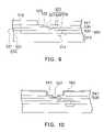
- FIG. 2a cross-sectional view schematically showing a chip structure according to a first embodiment of the present invention.
- a chip structure 200is provided with a substrate 210 , a first built-up layer 220 , a passivation layer 230 and a second built-up layer 240 .
- the first built-up layer 220is located on the substrate 210 .
- the first built-up layer 220is formed by cross lamination of first metal multi-layers 226 and first dielectric multi-layers.
- plugs 228connect the upper first metal layers 226 with the lower first metal layers 226 or connect the first metal layers 226 with the electric devices 214 .
- the first metal multi-layers 226 and the plugs 228compose a first interconnection scheme 222 .
- the first dielectric multi-layerscompose a first dielectric body 224 .
- the first interconnection scheme 222interlaces inside the first dielectric body 224 and is electrically connected to the electric devices 214 .
- the first interconnection scheme 222includes plenty of conductive pads 227 (only shows one of them) that are exposed outside the first dielectric body 224 .
- the first interconnection scheme 222can electrically connect with other circuits through the conductive pads 227 .
- the first dielectric body 224is made of, for example, an inorganic compound, such as a silicon oxide compound or a silicon nitride compound.
- the material of the first interconnection scheme 222includes, for example, copper, aluminum or tungsten.
- the first metal layers 226 and the plugs 228are made of copper.
- the first interconnection scheme 222is formed by a general process, the first metal layers 226 are made of aluminum and the plugs 228 are made of tungsten.
- the passivation layer 230is disposed on the first built-up layer 220 and is provided with openings exposing the conductive pads 227 .
- the passivation layer 230is constructed of, for example, an inorganic compound, such as a silicon oxide compound, a silicon nitride compound, phosphosilicate glass (PSG), a silicon oxide nitride compound or a composite formed by laminating the above material.
- an inorganic compoundsuch as a silicon oxide compound, a silicon nitride compound, phosphosilicate glass (PSG), a silicon oxide nitride compound or a composite formed by laminating the above material.
- the second built-up layer 240is formed on the passivation layer 230 .
- the second built-up layer 240is formed by cross lamination of second metal multi-layers 246 and second dielectric multi-layers 241 .
- via metal fillers 248connect the upper second metal layers 246 with the lower second metal layers 246 or connect the second metal layers 246 with the conductive pads 227 .
- the second metal layers 246 and the via metal fillers 248compose a second interconnection scheme 242 .
- the second dielectric multi-layers 241compose a second dielectric body 244 .
- the second interconnection scheme 242interlaces inside the second dielectric body 244 and is electrically connected to the conductive pads 227 .
- the second interconnection scheme 242includes plenty of nodes 247 (only shows one of them).
- the second dielectric body 244is provided with openings 249 exposing the nodes 247 of the second interconnection scheme 242 .
- the second interconnection scheme 242can electrically connect with external circuits through the nodes 247 .
- the second dielectric body 244is made of, for example, an organic compound, such as polyimide (PI), benzocyclobutene (BCB), porous dielectric material, parylene, elastomer, or other macromolecule polymers.
- the material of the second interconnection scheme 242includes, for example, copper, aluminum, gold, nickel, titanium-tungsten, titanium or chromium.
- the cross-sectional area A 2 of the traces of the second metal layers 246is extremely larger than the cross-sectional area A 1 of the traces of the first metal layers 226 and than the cross-sectional area of the plugs 228 .
- the cross-sectional area a of the via metal fillers 248is extremely larger than the cross-sectional area A 1 of the traces of the first metal layers 226 and than the cross-sectional area of the plugs 228 .
- the trace width d 2 of the second metal layers 246is extremely larger than the trace width d 1 of the first metal layers 226 .
- the trace thickness t 2 of the second metal layers 246is extremely larger than the trace thickness t 1 of the first metal layers 226 .
- the thickness L 2 of the individual second dielectric layers 241is extremely larger than the thickness L 1 of the individual first dielectric layers of the first built-up layers 220 .
- the cross-sectional area a of the via metal fillers 248is extremely larger than the area, exposed outside the passivation layer 230 , of the conductive pads 227 .
- the trace width d 2 of the second metal layers 246is larger than 1 micron, and preferably ranges from 1 micron to 1 centimeter.
- the trace thickness t 2 of the second metal layers 246is larger than 1 micron, and preferably ranges from 1 micron to 50 microns.
- the cross-sectional area A 2 of the second metal layers 246is larger than 1 square micron, and preferably ranges from 1 square micron to 0.5 square millimeters.
- the cross-sectional area a of the via metal fillers 248is larger than 1 square micron, and preferably ranges from 1 square micron to 10,000 square microns.
- the thickness L 2 of the individual second dielectric layers 241is larger than 1 micron, and preferably ranges from 1 micron to 100 microns.
- the above chip structurecan decline the resistance-capacitance delay, the power of the chip, and the temperature generated by the driving chip since the cross sectional area, the width and the thickness of the traces of the second metal layers 246 are extremely large, since the cross sectional area of the via metal fillers 248 is also extremely large, since the second interconnection scheme 242 can be made of low-resistance material, such as copper or gold, since the thickness L 2 of the individual second dielectric layers 241 is also extremely large, and since the second dielectric body 244 can be made of organic material, the dielectric constant of which is very low, approximately between 1.about.3, the practical value depending on the applied organic material.
- the traces of the second interconnection scheme 242are extremely wide and thick and the cross-sectional area of the via metal fillers 248 is extremely large.
- the second interconnection scheme 242can be formed by low-cost fabricating processes, such as an electroplating process, an electroless plating process, or a sputtering process, and, moreover, the second interconnection scheme 242 can be produced using facilities with low accuracy. Therefore, the production costs of the chip structure can be substantially saved.
- the request for the clean room where the second built-up layer is formedis not high, ranging from Class 10 to Class 100 . Consequently, the construction cost of the clean room can be conserved.
- the chip structurecan simplify a design of a substrate board due to the layout redistribution, fitting the design of the substrate board, of the nodes 247 of the chip structure by the second interconnection scheme 242 and, besides, the application of the fewer nodes 247 to which ground voltage or power voltage is applied.
- the layout redistribution of nodes 247 of various chips by the second interconnection scheme 242causes the above various chips to be provided with the same node layout
- the node layout, matching the same node layout of the above various chips, of the substrate boardcan be standardized. Therefore, the cost of fabricating the substrate board substantially drops off.
- FIG. 3is a cross-sectional view schematically showing a chip structure according to a second embodiment of the present invention.
- the first interconnection scheme 322 of the built-up layer 320electrically connects the second interconnection scheme 342 of the built-up layer 340 with the electric devices 314 and at least one electrostatic discharge circuit 316 , wherein the electrostatic discharge circuit 316 is disposed on the surface 312 of the substrate 310 .
- the second interconnection scheme 342electrically connects with the power ends of the electric devices 314 .
- the second interconnection scheme 342is designed as a ground bus, the second interconnection scheme 342 electrically connects with the ground ends of the electric devices 314 .
- the second metal layer 346 of the power bus or that of the ground buscan be of, for example, a planer type. According to the above chip structure, each of the power buses or the ground buses can electrically connect with more electric devices 314 than that of prior art. Consequently, the number of the power buses or the ground buses can be reduced and, also, the number of the electrostatic discharge circuits 316 accompanying the power buses or the ground buses can be reduced.
- the number of the nodes 347 accompanying the power buses or the ground busescan be reduced.
- the electrostatic discharge circuits 316can prevent the electric devices 314 electrically connected with the second interconnection scheme 344 from being damaged by the sudden discharge of high voltage.
- the chip structure 300can be electrically connected with external circuits through the nodes 347 applying a flip-chip type, a wire-bonding type or a tape-automated-bonding type.
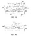
- FIG. 4is a cross-sectional view schematically showing a chip structure according to a third embodiment of the present invention.
- the first interconnection scheme 422is divided into first interconnections 422 a and first transition interconnections 422 b .
- the second interconnection scheme 442is divided into second interconnections 442 a and second transition interconnections 442 b .
- the nodes 447are electrically connected with the transition devices 418 and the electrostatic discharge circuits 416 through the first transition interconnections 422 b and the second transition interconnections 442 b .
- the transition devices 418are electrically connected with the electric devices 414 through the first interconnections 422 a and the second interconnections 442 a .
- this circuit layoutcan be to transmit clock signals.
- the electrostatic discharge circuits 416can prevent the electric devices 414 and the transition devices 418 from being damaged by the sudden discharge of high voltage.
- the chip structurecan be electrically connected with external circuits through the nodes 447 applying a flip-chip type, a wire-bonding type or a tape-automated-bonding type.
- FIG. 5is a cross-sectional view schematically showing a chip structure according to a forth embodiment of the present invention.
- the second metal layer 1546 of the second interconnection scheme 1542is directly formed on the passivation layer 1530 .
- the second metal layer 1546 of the second interconnection scheme 1542can be directly electrically connected with the conductive pads 1527 , exposed outside the passivation layer 1530 , of the first interconnection scheme 1522 .
- the chip structurecan be electrically connected with external circuits through the nodes 1547 applying a flip-chip type, a wire-bonding type or a tape-automated-bonding type.
- a second built-up layeris constructed from a second dielectric body and a second interconnection scheme.
- a second built-up layeralso can be composed of only a second interconnection scheme, as shown in FIG. 6 .
- FIG. 6is a cross-sectional view schematically showing a chip structure according to a fifth embodiment of the present invention.
- the second metal layer 1646 of the second interconnection schemeis directly formed on the passivation layer 1630 and can be directly electrically connected with the conductive pads 1627 , exposed outside the passivation layer 1630 , of the first interconnection scheme 1622 .
- the second metal layer 1646is exposed to the outside.
- the chip structurecan be electrically connected with external circuits by bonding wires onto the second metal layer 1646 .
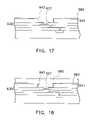
- FIG. 7is a cross-sectional view schematically showing a chip structure according to a sixth embodiment of the present invention.
- FIG. 8is a cross-sectional view schematically showing a chip structure according to a seventh embodiment of the present invention.
- the conductive pads 727 aare exposed to the outside and the conductive pads 727 b are directly electrically connected with the second metal layer 746 .
- the chip structure 700can be electrically connected with external circuits by bonding wires (not shown) onto the conductive pads 727 a .
- the first transition interconnections 722 bthe conductive pads 727 a are electrically connected with the electrostatic discharge circuits 716 and the transition devices 718 respectively.
- the transition devices 718are electrically connected with the electric devices 714 .
- bumpsalso can be formed on the conductive pads 727 a , and the chip structure 700 can be electrically connected with external circuits through the bumps.
- the conductive pads 827 aare exposed to the outside and the conductive pads 827 b are directly electrically connected with the second interconnection scheme 842 .
- Linking traces 829connect the conductive pads 827 a with the conductive pads 827 b .
- the chip structure 800can be electrically connected with external circuits by bonding wires (not shown) onto the conductive pads 827 a .
- the linking traces 829 and conductive pads 827 bthe conductive pads 827 a are electrically connected with the second interconnection scheme 842 .
- the first interconnection scheme 822the second interconnection scheme 842 is electrically connected with the electric devices 814 .
- bumpsalso can be formed on the conductive pads 827 a , and the chip structure 800 can be electrically connected with external circuits through the bumps.
- the shorter the length S of the linking traces 829the better the electrical efficiency of the chip structure 800 . Otherwise, it is possible that the resistance-capacitance delay and the voltage drop will occur and the chip efficiency will be reduced. It is preferred that the length S of the linking traces 829 is less than 5,000 microns.
- FIGS. 9-15are various cross-sectional views schematically showing a process of fabricating a chip structure according to an embodiment of the present invention.
- a wafer 502is provided with a substrate 510 , a first built-up layer 520 and a passivation layer 530 .
- the first built-up layer 520is formed on the substrate 510 .
- the first built-up layer 520includes a first interconnection scheme 522 and a first dielectric body 524 , wherein the first interconnection scheme 522 interlaces inside the first dielectric body 524 and is electrically connected to the electric devices 514 .
- the first dielectric body 524is constructed from the lamination of first dielectric multi-layers 521 .
- the first interconnection scheme 522includes first metal multi-layers 526 and plugs 528 . Through the plugs 528 , the first metal layers 526 can be electrically connected with the electric devices 514 or the first metal layers 526 neighbored.
- the first interconnection scheme 522further includes one or more conductive pads 527 (only shows one of them) that are exposed outside the first dielectric body 524 .
- the passivation layer 530is formed on the first built-up layer 520 and is provided with one or more openings 532 exposing the conductive pads 527 . The largest width of the openings 532 ranges from 0.5 to 200 microns for example.
- the openings 532can be formed relatively small, for example, the largest width of the openings 532 ranging from 0.5 to 20 microns, and, correspondingly, the conductive pads 527 can be formed relatively small, the routing density of the top metal layer having the conductive pads 527 can be enhanced. Moreover, due to the design of the openings 532 with relatively small dimensions and high density, correspondingly, the circuits, connecting with the conductive pads 527 , of the second interconnection scheme can be formed small. As a result, the parasitic capacitance generated by the second interconnection scheme can become relatively small.
- a second dielectric sub-layer 541is formed on the passivation layer 530 by, for example, a spin-coating process, wherein the second dielectric sub-layer 541 is made of, for instance, photosensitive organic material.
- one or more via metal openings 543are formed through the second dielectric sub-layer 541 using, for example, a photolithography process.
- the via metal openings 543expose the conductive pads 527 .
- the width of the openings 532is very small, such as 1 micron
- the width of the via metal openings 543can be designed to be larger than that of the openings 532 .
- the width of the via metal openings 543is 3 microns or larger than 3 microns.
- a conductive layer 560is formed onto the second dielectric sub-layer 541 , onto the side walls of the via metal openings 543 , and onto the passivation layer 530 and the conductive pads 527 exposed by the via metal openings 543 .
- the conductive layer 560is made of, for example, titanium-tungsten, titanium or chromium.
- a photoresist 550is formed onto the conductive layer 560 .
- photoresist openingsare formed where a second metal layer is demanded to be fabricated and pass through the photoresist 550 to expose the conductive layer 560 .
- one or more conductive metals 580are filled into the via metal openings 543 and the photoresist openings 552 as shown in FIG. 12 , and are formed over the conductive layer 560 .
- the conductive metals 580include copper, gold, or nickel.
- the photoresist 550is removed as shown in FIG. 13 .
- the conductive layer 560 exposed to the outsideis removed and only remains the conductive layer 560 disposed under the conductive metals 580 .
- another second dielectric sub-layer 570is formed onto the conductive metals 580 and onto the second dielectric sub-layer 541 located at the lower portion.
- the second dielectric sub-layer 570latest formed at the higher portion, is made of, for example, photosensitive material.
- the second built-up layer 540is completed so far.
- the second built-up layer 540includes a second interconnection scheme 542 and a second dielectric body 544 , wherein the second interconnection scheme 542 interlaces inside the second dielectric body 544 .
- the second interconnection scheme 542includes at least one second metal layer 546 and at least one via metal filler 548 .
- the via metal filler 548is constructed from the conductive metals 580 and the conductive layer 560 that are disposed in the via metal opening 543 .
- the second metal layer 546is constructed from the conductive metals 580 and the conductive layer 560 that are outside the via metal opening 543 and on the second dielectric sub-layer 541 .
- the via metal filler 548electrically connects the second metal layers 546 with the conductive pads 527 .
- the cross-sectional area of the opening 532is very small, the cross-sectional area of the via metal opening 543 can be designed to be larger than that of the opening 532 .
- the second dielectric body 544is constructed from the lamination of the second dielectric multi-layers 541 , 570 .
- the thickness L 2 of the second dielectric layers 541 , 570is extremely larger than the thickness L 1 of the first dielectric layers 521 .
- the thickness L 2 of the second dielectric layers 541 , 570ranges from 1 micron to 100 microns.
- the structure, material, and dimension of the second built-up layer 540are detailed in the previous embodiments, and the repeat is omitted herein.
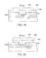
- FIGS. 16-22are various cross-sectional views schematically showing a process of fabricating a chip structure according to another embodiment of the present invention.
- a wafer 602is provided.
- the internal structure of the wafer 602is detailed as the previous embodiments, and the repeat is omitted herein.
- a second dielectric sub-layer 641is formed onto the passivation layer 630 of the wafer 602 by, for example, a spin-coating process, wherein the second dielectric sub-layer 641 is made of, for instance, photosensitive material.
- one or more via metal openings 643are formed through the second dielectric sub-layer 641 by, for example, a photolithography process. The via metal openings 643 expose the conductive pads 627 .
- the width of the via metal openings 643can be designed to be larger than that of the openings 632 . This leads conductive metals, during the following metal-filling process, to be easily filled into the via metal openings 643 and the openings 632 .
- a conductive layer 660is formed onto the second dielectric sub-layer 641 , onto the side walls of the via metal openings 643 , and onto the passivation layer 630 and the conductive pads 627 exposed by the via metal openings 643 .
- the conductive layer 660is made of, for example, titanium-tungsten, titanium or chromium.
- one or more conductive metals 680are formed onto the conductive layer 660 and into the via metal openings 643 , by, for example, an electroplating process or a sputtering process.
- the conductive metals 680include copper, aluminum, gold, or nickel.
- a photoresist 650is formed onto the conductive metals 680 and then by, for example, an exposure process and a lithography process, the photoresist 650 is defined with a line pattern. Only remains the photoresist 650 where a second metal layer is demanded to be formed, and the conductive metals 680 that is not demanded to be formed as the second metal layer is exposed to the outside.
- the conductive metals 680 exposed outside the photoresist 650are removed.
- the conductive layer 660 exposed outside the conductive metals 680are removed by, for example, another etching process.
- the photoresist 650is removed, as shown in FIG. 21 .
- another second dielectric sub-layer 670is formed onto the conductive metals 680 and onto the second dielectric sub-layer 641 located at the lower portion.
- the second dielectric sub-layer 670latest formed at the higher portion, is made of, for example, photosensitive material.
- one or more node openings 672are formed through the second dielectric sub-layer 670 located at the higher portion such that the node openings 672 expose the top conductive metal 680 .
- the exposed conductive metal 680is defined as nodes 647 , through which the chip structure 600 can be electrically connected with external circuits.
- the structure, material, and dimension of the second built-up layer 640are detailed in the previous embodiments, and the repeat is omitted herein.
- the present inventionis not limited to the application of the second metal layer with a signal layer.
- second metal multi-layersalso can be applied in the present invention.
- the fabrication method of the second metal multi-layersis to repeat the above fabrication method of the second metal layer with a single layer.
- the second built-up layer, with second metal multi-layers, fabricated by the above whatever processis finally formed with a second dielectric sub-layer having node openings that expose the second interconnection scheme to be electrically connected with external circuits.
- the whole surface of the second metal layer at the top portioncan be exposed to the outside, and through bumps or conducting wires, the second metal layer can be electrically connected with external circuits.
- the via metal openings of the second dielectric sub-layer at a higher portionexpose the second metal layer at a lower portion so that the conductive metals disposited in the via metal openings electrically connect the upper second metal layer with the lower second metal layer.
- the present inventionhas the following advantages:
- the chip structure of the present inventioncan decline the resistance-capacitance delay, the power of the chip, and the temperature generated by the driving chip since the cross sectional area, the width and the thickness of the traces of the second metal layer are extremely large, since the cross sectional area of the via metal filler is also extremely large, since the second interconnection scheme can be made of low-resistance material, such as copper or gold, since the thickness of the individual second dielectric layer is also extremely large, and since the second dielectric body can be made of organic material, the dielectric constant of which is very low, approximately between 1.about.3, the practical value depending on the applied organic material.
- each of the power buses or the ground busescan electrically connect with more electric devices than that of prior art. Consequently, the number of the power buses or the ground buses can be reduced and, also, the number of the electrostatic discharge circuits accompanying the power buses or the ground buses can be reduced. In addition, the number of the nodes accompanying the power buses or the ground buses can be reduced.
- the electrostatic discharge circuitscan prevent the electric devices electrically connected with the second interconnection scheme from being damaged by the sudden discharge of high voltage.
- the chip structure of the present inventioncan simplify a design of a substrate board due to the node layout redistribution, fitting the design of the substrate board, of the chip structure by the second interconnection scheme and, besides, the application of the fewer nodes to which ground voltage or power voltage is applied. Moreover, in case the node layout redistribution of various chips by the second interconnection scheme causes the above various chips to be provided with the same node layout, the node layout, matching the same node layout of the above various chips, of the substrate board can be standardized. Therefore, the cost of fabricating the substrate board substantially drops off.
- the second interconnection schemecan be produced using facilities with low accuracy. Therefore, production costs of the chip structure can substantially be reduced.
Landscapes
- Physics & Mathematics (AREA)
- Engineering & Computer Science (AREA)
- Computer Hardware Design (AREA)
- Microelectronics & Electronic Packaging (AREA)
- Power Engineering (AREA)
- Condensed Matter Physics & Semiconductors (AREA)
- General Physics & Mathematics (AREA)
- Geometry (AREA)
- Manufacturing & Machinery (AREA)
- Internal Circuitry In Semiconductor Integrated Circuit Devices (AREA)
- Semiconductor Integrated Circuits (AREA)
Abstract
Description
- This application is a continuation of application Ser. No. 10/997,145, filed on Nov. 24, 2004, now pending, which is a division of application Ser. No. 10/690,205, filed on Oct. 20, 2003, now U.S. Pat. No. 6,936,531, which is a division of application Ser. No. 10/337,673, filed on Jan. 6, 2003, now U.S. Pat. No. 6,700,162, which is a division of application Ser. No. 10/124,388, filed on Apr. 15, 2002, now U.S. Pat. No. 6,756,259.
- The present application is a continuation-in-part of a pending patent application Ser. No. 09/216,791, filed Dec. 21, 1998, by M. S. Lin. The present application is a continuation-in-part of a pending patent application Ser. No. 09/251,183, filed Feb. 17, 1999, by M. S. Lin. The present application is a continuation-in-part of a pending patent application Ser. No. 09/691,497, filed Oct. 18, 2000, by M. S. Lin and J. Y. Lee. The present application is a continuation-in-part of a pending patent application Ser. No. 09/972,639, filed Oct. 9, 2001, by M. S. Lin. All disclosures of these prior applications are incorporated herein by reference.
- 1. Field of the Invention
- The invention relates in general to a chip structure and a process for forming the same. More particularly, the invention relates to a chip structure for improving the resistance-capacitance delay and a forming process thereof.
- 2. Description of the Related Art
- Nowadays, electronic equipment are increasingly used to achieve many various tasks. With the development of electronics technology, miniaturization, multi-function task, and comfort of utilization are among the principle guidelines of electronic product manufacturers. More particularly in semiconductor manufacture process, the semiconductor devices with 0.18 microns have been mass-produced. However, the relatively fine interconnections therein negatively impact the chip. For example, this causes the voltage drop of the buses, the resistance-capacitor delay of the key traces, and noises, etc.
FIG. 1 is a cross-sectional view showing a conventional chip structure with interconnections.- As shown in
FIG. 1 , achip structure 100 is provided with asubstrate 110, an built-uplayer 120 and apassivation layer 130. There are plenty ofelectric devices 114, such as transistors, on asurface 112 of thesubstrate 110, wherein thesubstrate 110 is made of, for example, silicon. The built-uplayer 120 provided with adielectric body 122 and aninterconnection scheme 124 is formed on thesurface 112 of thesubstrate 110. Theinterconnection scheme 124 interlaces inside thedielectric body 122 and is electrically connected to theelectric devices 114. Further, theinterconnection scheme 124 includes manyconductive pads 126 exposed outside thedielectric body 122 and theinterconnection scheme 124 can electrically connect with external circuits through theconductive pads 126. Thedielectric body 122 is made of, for instance, silicon nitride or silicon oxide. In addition, thepassivation layer 130 is deposited on the built-uplayer 120, and has many openings respectively exposing theconductive pads 126. Theinterconnection scheme 124 includes at least one metal layer that can serve as a power bus or a ground bus. The power bus or the ground bus is connected to at least one of theconductive pads 126 through which the power bus or the ground bus can electrically connect with external circuits. - However, as far as the
chip structure 100 is concerned, resistance-capacitance (RC) delay is easily generated because the line width of theinterconnection scheme 124 is extremely fine, about below 0.3 microns, the thickness of theinterconnection scheme 124 is extremely thin, and the dielectric constant of thedielectric body 122 is extremely high, about 4. Therefore, the chip efficiency drops off. In particular, the RC delay even usually occurs with respect to a power bus, a ground bus or other metal lines transmitting common signals. In addition, the production of theinterconnection scheme 124 with extremely fine line width is necessarily performed using facilities with high accuracy. This causes production costs to dramatically rise. - The present invention is related to a R.O.C. patent application Ser. No. 88120548, filed Nov. 25, 1999, by M. S. Lin, issued Sep. 1, 2001, now R.O.C. Pat. No. 140721. R.O.C. patent application Ser. No. 88120548 claims the priority of pending U.S. patent application Ser. No. 09/251,183 and the subject matter thereof is disclosed in pending U.S. patent application Ser. No. 09/251,183. The present invention is related to a R.O.C. patent application Ser. No. 90100176, filed Jan. 4, 2001, by M. S. Lin and J. Y. Lee, now pending. The subject matter of R.O.C. patent application Ser. No. 90100176 is disclosed in pending U.S. patent application Ser. No. 09/691,497. The present invention is related to a Japanese patent application Ser. No. 200156759, filed Mar. 1, 2001, by M. S. Lin and J. Y. Lee, now pending. The present invention is related to a European patent application Ser. No. 01480077.5, filed Aug. 27, 2001, by M. S. Lin and J. Y. Lee, now pending. The present invention is related to a Singaporean patent application Ser. No. 200101847-2, filed Mar. 23, 2001, by M. S. Lin and J. Y. Lee, now pending. Japanese patent application Ser. No. 200156759, European patent application Ser. No. 01480077.5, and Singaporean patent application Ser. No. 200101847-2 claim the priority of pending U.S. patent application Ser. No. 09/691,497 and the subject matter of them is disclosed in pending U.S. patent application Ser. No. 09/691,497.
- Accordingly, an objective of the present invention is to provide a chip structure and a process for forming the same that improves resistance-capacitance delay and reduces energy loss of the chip.
- Another objective of the present invention is to provide a chip structure and a process for forming the same that can be produced using facilities with low accuracy. Therefore, production costs can substantially reduce.
- To achieve the foregoing and other objectives, the present invention provides a chip structure that comprises a substrate, a first built-up layer, a passivation layer and a second built-up layer. The substrate includes many electric devices placed on a surface of the substrate. The first built-up layer is located on the substrate. The first built-up layer is provided with a first dielectric body and a first interconnection scheme, wherein the first interconnection scheme interlaces inside the first dielectric body and is electrically connected to the electric devices. The first interconnection scheme is constructed from first metal layers and plugs, wherein the neighboring first metal layers are electrically connected through the plugs. The passivation layer is disposed on the first built-up layer and is provided with openings exposing the first interconnection scheme. The second built-up layer is formed on the passivation layer. The second built-up layer is provided with a second dielectric body and a second interconnection scheme, wherein the second interconnection scheme interlaces inside the second dielectric body and is electrically connected to the first interconnection scheme. The second interconnection scheme is constructed from at least one second metal layer and at least one via metal filler, wherein the second metal layer is electrically connected to the via metal filler. The thickness, width, and cross-sectional area of the traces of the second metal layer are respectively larger than those of the first metal layers. In addition, the first dielectric body is constructed from at least one first dielectric layer, and the second dielectric body is constructed from at least one second dielectric layer. The individual second dielectric layer is thicker than the individual first dielectric layer.
- According to a preferred embodiment of the present invention, the thickness of the traces of the second metal layer ranges from 1 micron to 50 microns; the width of the traces of the second metal layer ranges from 1 micron to 1 centimeter; the cross sectional area of the traces of the second metal layer ranges from 1 square micron to 0.5 square millimeters. The first dielectric body is made of, for example, an inorganic compound, such as a silicon nitride compound or a silicon oxide compound. The second dielectric body is made of, for example, an organic compound, such as polyimide (PI), benzocyclobutene (BCB), porous dielectric material, or elastomer. In addition, the above chip structure further includes at least one electrostatic discharge (ESD) circuit and at least one transitional device that are electrically connected to the first interconnection scheme. The transitional device can be a driver, a receiver or an I/O circuit. Moreover, the first interconnection scheme include at least one first conductive pad, at least one second conductive pad, and at least one linking trace, wherein the openings of the passivation layer expose the first conductive pad and the second conductive pad. The second conductive pad is electrically connected to the second interconnection scheme. The first conductive pad is exposed to the outside. The linking trace connects the first conductive pad with the second conductive pad and is shorter than 5,000 microns.
- To sum up, the chip structure of the present invention can decline the resistance-capacitance delay, the power of the chip, and the temperature generated by the driving chip since the cross sectional area, the width and the thickness of the traces of the second metal layer are extremely large, since the cross sectional area of the via metal filler is also extremely large, since the second interconnection scheme can be made of low-resistance material, such as copper or gold, since the thickness of the individual second dielectric layer is also extremely large, and since the second dielectric body can be made of organic material, the dielectric constant of which is very low, approximately between 1.about.3, the practical value depending on the applied organic material.
- In addition, the chip structure of the present invention can simplify a design of a substrate board due to the node layout redistribution, fitting the design of the substrate board, of the chip structure by the second interconnection scheme and, besides, the application of the fewer nodes to which ground voltage or power voltage is applied. Moreover, in case the node layout redistribution of various chips by the second interconnection scheme causes the above various chips to be provided with the same node layout, the node layout, matching the same node layout of the above various chips, of the substrate board can be standardized. Therefore, the cost of fabricating the substrate board substantially drops off.
- Moreover, according to the chip structure of the present invention, the second interconnection scheme can be produced using facilities with low accuracy. Therefore, production costs of the chip structure can substantially be reduced.
- To achieve the foregoing and other objectives, the present invention provides a process for making the above chip structure. The process for fabricating a chip structure comprises the following steps.
- Step 1: A wafer is provided with a plurality of electric devices, an interconnection scheme and a passivation layer. Both the electric devices and the interconnection scheme are arranged inside the wafer. The interconnection scheme is electrically connected with the electric devices. The passivation layer is disposed on a surface layer of the wafer. The passivation layer has at least one opening exposing the interconnection scheme. The largest width of the opening of the passivation ranges from 0.5 microns to 200 microns
- Step 2: A conductive layer is formed over the passivation layer of the wafer by, for example, a sputtering process, and the conductive layer is electrically connected with the interconnection scheme.
- Step 3: A photoresist is formed onto the conductive layer, and the photoresist has at least one opening exposing the conductive layer.
- Step 4: At least one conductive metal is filled into the opening of the photoresist by, for example, a electroplating process, and the conductive metal is disposed over the conductive layer.
- Step 5: The photoresist is removed.
- Step 6: The conductive layer exposed to the outside is removed by, for example, an etching process, and the conductive layer deposited under the conductive metal remains. A signal is transmitted from one of the electric devices to the interconnection scheme, then passes through the passivation layer, and finally is transmitted to the conductive metal, and further, the signal is transmitted from the conductive metal to the interconnection scheme with passing through the passivation layer, and finally is transmitted to the other one or more of the electric devices.
- Provided that two metal layers are to be formed, the process for fabricating the above chip structure further comprises the following steps:
- Step 7: A dielectric sub-layer is formed over the passivation layer and covers the formed conductive metal. The dielectric sub-layer has at least one opening exposing the conductive metal formed at a lower portion.
- Step 8: At least other one conductive layer is formed on the dielectric sub-layer and into the opening of the dielectric sub-layer by, for example, a sputtering process. The other conductive layer is electrically connected with the metal layer exposed by the opening of the dielectric sub-layer.
- Step 9: A photoresist is formed onto the other conductive layer, and the photoresist having at least one opening exposing the other conductive layer.
- Step 10: At least other one conductive metal is filled into the opening of the photoresist by, for example, an electroplating process, and the other conductive metal disposed over the other conductive layer.
- Step 11: The photoresist is removed.
- Step 12: The other conductive layer exposed to the outside is removed by, for example, an etching process, and the other conductive layer deposited under the other conductive metal remains.
- Provided that multiple metal layers are to be formed, the sequential steps7-12 are repeated at least one time.
- To achieve the foregoing and other objectives, the present invention provides another process for making the above chip structure. The process for fabricating a chip structure comprises the following steps.
- Step 1: A wafer is provided with a plurality of electric devices, an interconnection scheme and a passivation layer. Both the electric devices and the interconnection scheme are arranged inside the wafer. The interconnection scheme is electrically connected with the electric devices. The passivation layer is disposed on a surface layer of the wafer. The passivation layer has at least one opening exposing the interconnection scheme.
- Step 2: At least one conductive metal is formed over the passivation layer of the wafer by, for example, a sputtering process, and the conductive metal is electrically connected with the interconnection scheme.
- Step 3: A photoresist is formed onto the conductive metal, and the photoresist is patterned to expose the conductive metal to the outside.
- Step 4: The conductive metal exposed to the outside is removed, and the conductive metal deposited under the photoresist remains.
- Step 5: The photoresist is removed.
- Provided that two metal layers are to be formed, the process for fabricating the above chip structure further comprises the following steps:
- Step 6: A dielectric sub-layer is formed over the passivation layer and covers the formed conductive metal. The dielectric sub-layer has at least one opening exposing the conductive metal formed at a lower portion.
- Step 7: At least other one conductive metal is formed over the passivation layer of the wafer by, for example, a sputtering process, and the other conductive metal electrically is connected with the conductive metal formed at a lower portion.
- Step 8: A photoresist is formed onto the other conductive metal, and the photoresist is patterned to expose the other conductive metal to the outside.
- Step 9: The other conductive metal exposed to the outside is removed, and the other conductive metal deposited under the photoresist remains.
- Step 10: The photoresist is removed.
- Provided that multiple metal layers are to be formed, the sequential steps6-10 are repeated at least one time.
- Both the foregoing general description and the following detailed description are exemplary and explanatory only and are not restrictive of the invention, as claimed. It is to be understood that both the foregoing general description and the following detailed description are exemplary, and are intended to provide further explanation of the invention as claimed.
- The accompanying drawings are included to provide a further understanding of the invention, and are incorporated in and constitute a part of this specification. The drawings illustrate embodiments of the invention and, together with the description, serve to explain the principles of the invention. A simple description of the drawings is as follows.
FIG. 1 is a cross-sectional view schematically showing a conventional chip structure with interconnections.FIG. 2 is a cross-sectional view schematically showing a chip structure according to a first embodiment of the present invention.FIG. 3 is a cross-sectional view schematically showing a chip structure according to a second embodiment of the present invention.FIG. 4 is a cross-sectional view schematically showing a chip structure according to a third embodiment of the present invention.FIG. 5 is a cross-sectional view schematically showing a chip structure according to a forth embodiment of the present invention.FIG. 6 is a cross-sectional view schematically showing a chip structure according to a fifth embodiment of the present invention.FIG. 7 is a cross-sectional view schematically showing a chip structure according to a sixth embodiment of the present invention.FIG. 8 is a cross-sectional view schematically showing a chip structure according to a seventh embodiment of the present invention.FIGS. 9-15 are various cross-sectional views schematically showing a process of fabricating a chip structure according to an embodiment of the present invention.FIGS. 16-22 are various cross-sectional views schematically showing a process of fabricating a chip structure according to another embodiment of the present invention.- Prior to describing the embodiment of the invention, the factors of the resistance-capacitance delay and those of the power loss will be introduced as the following equations.
τ=RC=2∈ρL[L(Tu.d.Tm)+L/(WS)]
P∝2πfV2k∈(tan δ)- where .tau. is effect of resistance-capacitance delay; P is power loss; .∈ is dielectric constant of dielectric material; ρ is resistance of traces; L is trace length; W is trace width; S is pitch between traces; Tu.d.is thickness of dielectric material; Tmis trace thickness; tan δ is dielectric loss; V is applied voltage; f is frequency; k is factor of capacitor structure.
- According to the above equation, the factors of the resistance-capacitance delay and those of the power loss can be known. Therefore, an increase in thickness of every dielectric layer, an application of dielectric material with low dielectric constant, an application of traces with low resistance, or an increase in width or thickness of traces leads an effect of a resistance-capacitance delay and a power loss of a chip to decline.
- According to the above conception, the present invention provides various improved chip structure. Please refer to
FIG. 2 , a cross-sectional view schematically showing a chip structure according to a first embodiment of the present invention. A chip structure200 is provided with asubstrate 210, a first built-uplayer 220, apassivation layer 230 and a second built-uplayer 240. There are plenty ofelectric devices 214, such as transistors, on asurface 212 of thesubstrate 210, wherein thesubstrate 210 is made of, for example, silicon. The first built-uplayer 220 is located on thesubstrate 210. The first built-uplayer 220 is formed by cross lamination offirst metal multi-layers 226 and first dielectric multi-layers. Moreover, plugs228 connect the upperfirst metal layers 226 with the lowerfirst metal layers 226 or connect thefirst metal layers 226 with theelectric devices 214. Thefirst metal multi-layers 226 and theplugs 228 compose afirst interconnection scheme 222. The first dielectric multi-layers compose a firstdielectric body 224. Thefirst interconnection scheme 222 interlaces inside the firstdielectric body 224 and is electrically connected to theelectric devices 214. Thefirst interconnection scheme 222 includes plenty of conductive pads227 (only shows one of them) that are exposed outside the firstdielectric body 224. Thefirst interconnection scheme 222 can electrically connect with other circuits through theconductive pads 227. The firstdielectric body 224 is made of, for example, an inorganic compound, such as a silicon oxide compound or a silicon nitride compound. The material of thefirst interconnection scheme 222 includes, for example, copper, aluminum or tungsten. Provided that thefirst interconnection scheme 222 is formed by a copper process, thefirst metal layers 226 and theplugs 228 are made of copper. Provided that thefirst interconnection scheme 222 is formed by a general process, thefirst metal layers 226 are made of aluminum and theplugs 228 are made of tungsten. - The
passivation layer 230 is disposed on the first built-uplayer 220 and is provided with openings exposing theconductive pads 227. Thepassivation layer 230 is constructed of, for example, an inorganic compound, such as a silicon oxide compound, a silicon nitride compound, phosphosilicate glass (PSG), a silicon oxide nitride compound or a composite formed by laminating the above material. - The second built-up
layer 240 is formed on thepassivation layer 230. The second built-uplayer 240 is formed by cross lamination ofsecond metal multi-layers 246 and seconddielectric multi-layers 241. Moreover, viametal fillers 248 connect the uppersecond metal layers 246 with the lowersecond metal layers 246 or connect thesecond metal layers 246 with theconductive pads 227. Thesecond metal layers 246 and the viametal fillers 248 compose asecond interconnection scheme 242. The seconddielectric multi-layers 241 compose a second dielectric body244. Thesecond interconnection scheme 242 interlaces inside the second dielectric body244 and is electrically connected to theconductive pads 227. Thesecond interconnection scheme 242 includes plenty of nodes247 (only shows one of them). The second dielectric body244 is provided withopenings 249 exposing thenodes 247 of thesecond interconnection scheme 242. Thesecond interconnection scheme 242 can electrically connect with external circuits through thenodes 247. The second dielectric body244 is made of, for example, an organic compound, such as polyimide (PI), benzocyclobutene (BCB), porous dielectric material, parylene, elastomer, or other macromolecule polymers. The material of thesecond interconnection scheme 242 includes, for example, copper, aluminum, gold, nickel, titanium-tungsten, titanium or chromium. Because mobile ions and moisture of the second built-uplayer 240 can be prevented by thepassivation layer 230 from penetrating into the first built-uplayer 220 or theelectric devices 214, it is practicable that an organic compound and various metals are formed over thepassivationtion layer 230. The cross-sectional area A2 of the traces of the second metal layers246 is extremely larger than the cross-sectional area A1 of the traces of thefirst metal layers 226 and than the cross-sectional area of theplugs 228. The cross-sectional area a of the viametal fillers 248 is extremely larger than the cross-sectional area A1 of the traces of thefirst metal layers 226 and than the cross-sectional area of theplugs 228. The trace width d2 of the second metal layers246 is extremely larger than the trace width d1 of the first metal layers226. The trace thickness t2 of the second metal layers246 is extremely larger than the trace thickness t1 of the first metal layers226. The thickness L2 of the individual seconddielectric layers 241 is extremely larger than the thickness L1 of the individual first dielectric layers of the first built-uplayers 220. The cross-sectional area a of the viametal fillers 248 is extremely larger than the area, exposed outside thepassivation layer 230, of theconductive pads 227. The trace width d2 of the second metal layers246 is larger than 1 micron, and preferably ranges from 1 micron to 1 centimeter. The trace thickness t2 of the second metal layers246 is larger than 1 micron, and preferably ranges from 1 micron to 50 microns. The cross-sectional area A2 of the second metal layers246 is larger than 1 square micron, and preferably ranges from 1 square micron to 0.5 square millimeters. The cross-sectional area a of the viametal fillers 248 is larger than 1 square micron, and preferably ranges from 1 square micron to 10,000 square microns. The thickness L2 of the individual seconddielectric layers 241 is larger than 1 micron, and preferably ranges from 1 micron to 100 microns. - The above chip structure can decline the resistance-capacitance delay, the power of the chip, and the temperature generated by the driving chip since the cross sectional area, the width and the thickness of the traces of the
second metal layers 246 are extremely large, since the cross sectional area of the viametal fillers 248 is also extremely large, since thesecond interconnection scheme 242 can be made of low-resistance material, such as copper or gold, since the thickness L2 of the individual seconddielectric layers 241 is also extremely large, and since the second dielectric body244 can be made of organic material, the dielectric constant of which is very low, approximately between 1.about.3, the practical value depending on the applied organic material. - According to the above chip structure, the traces of the
second interconnection scheme 242 are extremely wide and thick and the cross-sectional area of the viametal fillers 248 is extremely large. Thus, thesecond interconnection scheme 242 can be formed by low-cost fabricating processes, such as an electroplating process, an electroless plating process, or a sputtering process, and, moreover, thesecond interconnection scheme 242 can be produced using facilities with low accuracy. Therefore, the production costs of the chip structure can be substantially saved. In addition, the request for the clean room where the second built-up layer is formed is not high, ranging from Class10 toClass 100. Consequently, the construction cost of the clean room can be conserved. - The chip structure can simplify a design of a substrate board due to the layout redistribution, fitting the design of the substrate board, of the
nodes 247 of the chip structure by thesecond interconnection scheme 242 and, besides, the application of thefewer nodes 247 to which ground voltage or power voltage is applied. Moreover, in case the layout redistribution ofnodes 247 of various chips by thesecond interconnection scheme 242 causes the above various chips to be provided with the same node layout, the node layout, matching the same node layout of the above various chips, of the substrate board can be standardized. Therefore, the cost of fabricating the substrate board substantially drops off. - Next, other preferred embodiments of the present invention will be introduced. As a lot of electric devices are electrically connected with a power bus and a ground bus, the current through the power bus and the ground bus is relatively large. Therefore, the second interconnection scheme of the second built-up layer can be designed as a power bus or a ground bus, as shown in
FIG. 3 .FIG. 3 is a cross-sectional view schematically showing a chip structure according to a second embodiment of the present invention. Thefirst interconnection scheme 322 of the built-uplayer 320 electrically connects thesecond interconnection scheme 342 of the built-uplayer 340 with theelectric devices 314 and at least oneelectrostatic discharge circuit 316, wherein theelectrostatic discharge circuit 316 is disposed on thesurface 312 of thesubstrate 310. As a result, provided that thesecond interconnection scheme 342 is designed as a power bus, thesecond interconnection scheme 342 electrically connects with the power ends of theelectric devices 314. Provided that thesecond interconnection scheme 342 is designed as a ground bus, thesecond interconnection scheme 342 electrically connects with the ground ends of theelectric devices 314. Thesecond metal layer 346 of the power bus or that of the ground bus can be of, for example, a planer type. According to the above chip structure, each of the power buses or the ground buses can electrically connect with moreelectric devices 314 than that of prior art. Consequently, the number of the power buses or the ground buses can be reduced and, also, the number of theelectrostatic discharge circuits 316 accompanying the power buses or the ground buses can be reduced. In addition, the number of thenodes 347 accompanying the power buses or the ground buses can be reduced. Thus, the circuit layout can be simplified and the production cost of thechip structure 300 can be saved. Theelectrostatic discharge circuits 316 can prevent theelectric devices 314 electrically connected with thesecond interconnection scheme 344 from being damaged by the sudden discharge of high voltage. In addition, thechip structure 300 can be electrically connected with external circuits through thenodes 347 applying a flip-chip type, a wire-bonding type or a tape-automated-bonding type. - Referring to
FIG. 4 ,FIG. 4 is a cross-sectional view schematically showing a chip structure according to a third embodiment of the present invention. There are manyelectric devices 414, many electrostatic discharge circuits416 (only shows one of them) and many transition devices418 (only shows one of them) on thesurface 412 of thesubstrate 410. Thefirst interconnection scheme 422 is divided intofirst interconnections 422aandfirst transition interconnections 422b. Thesecond interconnection scheme 442 is divided intosecond interconnections 442aandsecond transition interconnections 442b. Consequently, thenodes 447 are electrically connected with thetransition devices 418 and theelectrostatic discharge circuits 416 through thefirst transition interconnections 422band thesecond transition interconnections 442b. Thetransition devices 418 are electrically connected with theelectric devices 414 through thefirst interconnections 422aand thesecond interconnections 442a. For example, this circuit layout can be to transmit clock signals. Theelectrostatic discharge circuits 416 can prevent theelectric devices 414 and thetransition devices 418 from being damaged by the sudden discharge of high voltage. In addition, the chip structure can be electrically connected with external circuits through thenodes 447 applying a flip-chip type, a wire-bonding type or a tape-automated-bonding type. - Referring to
FIG. 5 ,FIG. 5 is a cross-sectional view schematically showing a chip structure according to a forth embodiment of the present invention. The second metal layer1546 of thesecond interconnection scheme 1542 is directly formed on thepassivation layer 1530. Thus, the second metal layer1546 of thesecond interconnection scheme 1542 can be directly electrically connected with theconductive pads 1527, exposed outside thepassivation layer 1530, of thefirst interconnection scheme 1522. In addition, the chip structure can be electrically connected with external circuits through thenodes 1547 applying a flip-chip type, a wire-bonding type or a tape-automated-bonding type. - According to the above embodiment, a second built-up layer is constructed from a second dielectric body and a second interconnection scheme. However, a second built-up layer also can be composed of only a second interconnection scheme, as shown in
FIG. 6 .FIG. 6 is a cross-sectional view schematically showing a chip structure according to a fifth embodiment of the present invention. Thesecond metal layer 1646 of the second interconnection scheme is directly formed on thepassivation layer 1630 and can be directly electrically connected with theconductive pads 1627, exposed outside thepassivation layer 1630, of thefirst interconnection scheme 1622. Thesecond metal layer 1646 is exposed to the outside. In addition, the chip structure can be electrically connected with external circuits by bonding wires onto thesecond metal layer 1646. - According to the above chip structure, bumps or wires are directly electrically connected with the second interconnection layer. However, the application of the present invention is not limited to the above embodiment. Bumps or wires also can be directly connected with conductive pads and, besides, through the first interconnection scheme, the bumps or the wires can be electrically connected with the second interconnection scheme, as shown in
FIG. 7 andFIG. 8 .FIG. 7 is a cross-sectional view schematically showing a chip structure according to a sixth embodiment of the present invention.FIG. 8 is a cross-sectional view schematically showing a chip structure according to a seventh embodiment of the present invention. - Referring to
FIG. 7 , in thechip structure 700, theconductive pads 727aare exposed to the outside and theconductive pads 727bare directly electrically connected with thesecond metal layer 746. Thechip structure 700 can be electrically connected with external circuits by bonding wires (not shown) onto theconductive pads 727a. Though thefirst transition interconnections 722b, theconductive pads 727aare electrically connected with theelectrostatic discharge circuits 716 and thetransition devices 718 respectively. Though thefirst interconnections 722a, theconductive pads 727band thesecond metal layer 746, thetransition devices 718 are electrically connected with theelectric devices 714. In addition, bumps also can be formed on theconductive pads 727a, and thechip structure 700 can be electrically connected with external circuits through the bumps. - Referring to
FIG. 8 , in thechip structure 800, theconductive pads 827aare exposed to the outside and theconductive pads 827bare directly electrically connected with thesecond interconnection scheme 842. Linking traces829 connect theconductive pads 827awith theconductive pads 827b. Thechip structure 800 can be electrically connected with external circuits by bonding wires (not shown) onto theconductive pads 827a. Though the linking traces829 andconductive pads 827b, theconductive pads 827aare electrically connected with thesecond interconnection scheme 842. Though thefirst interconnection scheme 822, thesecond interconnection scheme 842 is electrically connected with theelectric devices 814. In addition, bumps (not shown) also can be formed on theconductive pads 827a, and thechip structure 800 can be electrically connected with external circuits through the bumps. The shorter the length S of the linking traces829, the better the electrical efficiency of thechip structure 800. Otherwise, it is possible that the resistance-capacitance delay and the voltage drop will occur and the chip efficiency will be reduced. It is preferred that the length S of the linking traces829 is less than 5,000 microns. - Following, the second built-up layer of the present invention will be described.
FIGS. 9-15 are various cross-sectional views schematically showing a process of fabricating a chip structure according to an embodiment of the present invention. - First, referring to
FIG. 9 , awafer 502 is provided with asubstrate 510, a first built-uplayer 520 and apassivation layer 530. There are plenty ofelectric devices 514 on asurface 512 of thesubstrate 510. The first built-uplayer 520 is formed on thesubstrate 510. The first built-uplayer 520 includes afirst interconnection scheme 522 and a firstdielectric body 524, wherein thefirst interconnection scheme 522 interlaces inside the firstdielectric body 524 and is electrically connected to theelectric devices 514. The firstdielectric body 524 is constructed from the lamination of firstdielectric multi-layers 521. Thefirst interconnection scheme 522 includes first metal multi-layers526 and plugs528. Through the plugs528, the first metal layers526 can be electrically connected with theelectric devices 514 or the first metal layers526 neighbored. Thefirst interconnection scheme 522 further includes one or more conductive pads527 (only shows one of them) that are exposed outside the firstdielectric body 524. Thepassivation layer 530 is formed on the first built-uplayer 520 and is provided with one ormore openings 532 exposing theconductive pads 527. The largest width of theopenings 532 ranges from 0.5 to 200 microns for example. Because theopenings 532 can be formed relatively small, for example, the largest width of theopenings 532 ranging from 0.5 to 20 microns, and, correspondingly, theconductive pads 527 can be formed relatively small, the routing density of the top metal layer having theconductive pads 527 can be enhanced. Moreover, due to the design of theopenings 532 with relatively small dimensions and high density, correspondingly, the circuits, connecting with theconductive pads 527, of the second interconnection scheme can be formed small. As a result, the parasitic capacitance generated by the second interconnection scheme can become relatively small. - Next, a second
dielectric sub-layer 541 is formed on thepassivation layer 530 by, for example, a spin-coating process, wherein the seconddielectric sub-layer 541 is made of, for instance, photosensitive organic material. Subsequently, one or more viametal openings 543 are formed through the seconddielectric sub-layer 541 using, for example, a photolithography process. The viametal openings 543 expose theconductive pads 527. In case that the width of theopenings 532 is very small, such as 1 micron, the width of the viametal openings 543 can be designed to be larger than that of theopenings 532. This leads conductive metals, during the following metal-filling process, to be easily filled into the viametal openings 543 and theopenings 532. For instance, the width of the viametal openings 543 is 3 microns or larger than 3 microns. - Next, referring to
FIG. 10 , by, for example, a sputtering process, aconductive layer 560 is formed onto the seconddielectric sub-layer 541, onto the side walls of the viametal openings 543, and onto thepassivation layer 530 and theconductive pads 527 exposed by the viametal openings 543. Theconductive layer 560 is made of, for example, titanium-tungsten, titanium or chromium. Subsequently, as shown inFIG. 11 , aphotoresist 550 is formed onto theconductive layer 560. Then, by, for example, an exposing process and a lithography process, photoresist openings are formed where a second metal layer is demanded to be fabricated and pass through thephotoresist 550 to expose theconductive layer 560. Subsequently, by, for example, an electroplating process, one or moreconductive metals 580 are filled into the viametal openings 543 and thephotoresist openings 552 as shown inFIG. 12 , and are formed over theconductive layer 560. Foe example, theconductive metals 580 include copper, gold, or nickel. Thereafter, thephotoresist 550 is removed as shown inFIG. 13 . - Following, referring to
FIG. 14 , theconductive layer 560 exposed to the outside is removed and only remains theconductive layer 560 disposed under theconductive metals 580. Next, referring toFIG. 15 , by, for example, a spin-coating process, another seconddielectric sub-layer 570 is formed onto theconductive metals 580 and onto the seconddielectric sub-layer 541 located at the lower portion. The seconddielectric sub-layer 570, latest formed at the higher portion, is made of, for example, photosensitive material. Subsequently, by, for example, a photolithography process, one ormore node openings 572 are formed through the seconddielectric sub-layer 570 located at the higher portion such that thenode openings 572 expose the topconductive metal 580. The exposedconductive metal 580 is defined asnodes 547, through which thechip structure 500 can be electrically connected with external circuits. The second built-uplayer 540 is completed so far. The second built-uplayer 540 includes asecond interconnection scheme 542 and a seconddielectric body 544, wherein thesecond interconnection scheme 542 interlaces inside the seconddielectric body 544. Thesecond interconnection scheme 542 includes at least onesecond metal layer 546 and at least one viametal filler 548. The viametal filler 548 is constructed from theconductive metals 580 and theconductive layer 560 that are disposed in the viametal opening 543. Thesecond metal layer 546 is constructed from theconductive metals 580 and theconductive layer 560 that are outside the viametal opening 543 and on the seconddielectric sub-layer 541. The viametal filler 548 electrically connects thesecond metal layers 546 with theconductive pads 527. When the cross-sectional area of theopening 532 is very small, the cross-sectional area of the viametal opening 543 can be designed to be larger than that of theopening 532. The seconddielectric body 544 is constructed from the lamination of the seconddielectric multi-layers dielectric layers dielectric layers layer 540 are detailed in the previous embodiments, and the repeat is omitted herein. - Besides, the chip structure of the present invention can also be performed by the other process, described as follows.
FIGS. 16-22 are various cross-sectional views schematically showing a process of fabricating a chip structure according to another embodiment of the present invention. - First, referring to
FIG. 16 , awafer 602 is provided. The internal structure of thewafer 602 is detailed as the previous embodiments, and the repeat is omitted herein. Next, a seconddielectric sub-layer 641 is formed onto thepassivation layer 630 of thewafer 602 by, for example, a spin-coating process, wherein the seconddielectric sub-layer 641 is made of, for instance, photosensitive material. Subsequently, one or more viametal openings 643 are formed through the seconddielectric sub-layer 641 by, for example, a photolithography process. The viametal openings 643 expose theconductive pads 627. In case that the width of theopenings 632 is very small, the width of the viametal openings 643 can be designed to be larger than that of theopenings 632. This leads conductive metals, during the following metal-filling process, to be easily filled into the viametal openings 643 and theopenings 632. - Subsequently, referring to
FIG. 17 , by, for example, a sputtering process, aconductive layer 660 is formed onto the seconddielectric sub-layer 641, onto the side walls of the viametal openings 643, and onto thepassivation layer 630 and theconductive pads 627 exposed by the viametal openings 643. Theconductive layer 660 is made of, for example, titanium-tungsten, titanium or chromium. - Following, referring to
FIG. 18 , one or moreconductive metals 680 are formed onto theconductive layer 660 and into the viametal openings 643, by, for example, an electroplating process or a sputtering process. Foe example, theconductive metals 680 include copper, aluminum, gold, or nickel. Thereafter, referring toFIG. 19 , aphotoresist 650 is formed onto theconductive metals 680 and then by, for example, an exposure process and a lithography process, thephotoresist 650 is defined with a line pattern. Only remains thephotoresist 650 where a second metal layer is demanded to be formed, and theconductive metals 680 that is not demanded to be formed as the second metal layer is exposed to the outside. Subsequently, referring toFIG. 20 , by, for example, an etching process, theconductive metals 680 exposed outside thephotoresist 650 are removed. Thereafter, theconductive layer 660 exposed outside theconductive metals 680 are removed by, for example, another etching process. Next, thephotoresist 650 is removed, as shown inFIG. 21 . - Next, referring to
FIG. 22 , by, for example, a spin-coating process, another seconddielectric sub-layer 670 is formed onto theconductive metals 680 and onto the seconddielectric sub-layer 641 located at the lower portion. The seconddielectric sub-layer 670, latest formed at the higher portion, is made of, for example, photosensitive material. Subsequently, by, for example, a photolithography process, one ormore node openings 672 are formed through the seconddielectric sub-layer 670 located at the higher portion such that thenode openings 672 expose the topconductive metal 680. The exposedconductive metal 680 is defined asnodes 647, through which thechip structure 600 can be electrically connected with external circuits. The structure, material, and dimension of the second built-uplayer 640 are detailed in the previous embodiments, and the repeat is omitted herein. - In addition, according to the above process, the present invention is not limited to the application of the second metal layer with a signal layer. However, second metal multi-layers also can be applied in the present invention. The fabrication method of the second metal multi-layers is to repeat the above fabrication method of the second metal layer with a single layer. The second built-up layer, with second metal multi-layers, fabricated by the above whatever process is finally formed with a second dielectric sub-layer having node openings that expose the second interconnection scheme to be electrically connected with external circuits. Alternatively, the whole surface of the second metal layer at the top portion can be exposed to the outside, and through bumps or conducting wires, the second metal layer can be electrically connected with external circuits. Besides, when the second metal layers is over 2 layers, the via metal openings of the second dielectric sub-layer at a higher portion expose the second metal layer at a lower portion so that the conductive metals disposited in the via metal openings electrically connect the upper second metal layer with the lower second metal layer.
- To sum up, the present invention has the following advantages:
- 1. The chip structure of the present invention can decline the resistance-capacitance delay, the power of the chip, and the temperature generated by the driving chip since the cross sectional area, the width and the thickness of the traces of the second metal layer are extremely large, since the cross sectional area of the via metal filler is also extremely large, since the second interconnection scheme can be made of low-resistance material, such as copper or gold, since the thickness of the individual second dielectric layer is also extremely large, and since the second dielectric body can be made of organic material, the dielectric constant of which is very low, approximately between 1.about.3, the practical value depending on the applied organic material.
- 2. According to the chip structure of the present invention, each of the power buses or the ground buses can electrically connect with more electric devices than that of prior art. Consequently, the number of the power buses or the ground buses can be reduced and, also, the number of the electrostatic discharge circuits accompanying the power buses or the ground buses can be reduced. In addition, the number of the nodes accompanying the power buses or the ground buses can be reduced. Thus, the circuit layout can be simplified and the production cost of the chip structure can be saved. The electrostatic discharge circuits can prevent the electric devices electrically connected with the second interconnection scheme from being damaged by the sudden discharge of high voltage.
- 3. The chip structure of the present invention can simplify a design of a substrate board due to the node layout redistribution, fitting the design of the substrate board, of the chip structure by the second interconnection scheme and, besides, the application of the fewer nodes to which ground voltage or power voltage is applied. Moreover, in case the node layout redistribution of various chips by the second interconnection scheme causes the above various chips to be provided with the same node layout, the node layout, matching the same node layout of the above various chips, of the substrate board can be standardized. Therefore, the cost of fabricating the substrate board substantially drops off.
- 4. According to the chip structure of the present invention, the second interconnection scheme can be produced using facilities with low accuracy. Therefore, production costs of the chip structure can substantially be reduced.
- It will be apparent to those skilled in the art that various modifications and variations can be made to the structure of the present invention without departing from the scope or spirit of the invention. In view of the foregoing, it is intended that the present invention cover modifications and variations of this invention provided they fall within the scope of the following claims and their equivalents.
Claims (20)
Priority Applications (2)
| Application Number | Priority Date | Filing Date | Title |
|---|---|---|---|
| US12/024,998US8008776B2 (en) | 2001-12-13 | 2008-02-02 | Chip structure and process for forming the same |
| US13/191,356US8546947B2 (en) | 2001-12-13 | 2011-07-26 | Chip structure and process for forming the same |
Applications Claiming Priority (13)
| Application Number | Priority Date | Filing Date | Title |
|---|---|---|---|
| TW090130876ATW519707B (en) | 2001-12-13 | 2001-12-13 | Chip structure with passivation layer having outer layer connection and its manufacturing process |
| TW90130876 | 2001-12-13 | ||
| TW90130876A | 2001-12-13 | ||
| TW90131030 | 2001-12-14 | ||
| TW90131030A | 2001-12-14 | ||
| TW90131030ATW511243B (en) | 2001-12-14 | 2001-12-14 | Chip structure and process for making the same |
| TW90131796 | 2001-12-21 | ||
| TW90131796ATW519726B (en) | 2001-12-21 | 2001-12-21 | Chip structure and its process |
| TW90131796A | 2001-12-21 | ||
| US10/124,388US6756295B2 (en) | 1998-12-21 | 2002-04-15 | Chip structure and process for forming the same |
| US10/690,250US6936531B2 (en) | 1998-12-21 | 2003-10-20 | Process of fabricating a chip structure |
| US10/997,145US7470988B2 (en) | 1998-12-21 | 2004-11-24 | Chip structure and process for forming the same |
| US12/024,998US8008776B2 (en) | 2001-12-13 | 2008-02-02 | Chip structure and process for forming the same |
Related Parent Applications (1)
| Application Number | Title | Priority Date | Filing Date |
|---|---|---|---|
| US10/997,145ContinuationUS7470988B2 (en) | 1998-12-21 | 2004-11-24 | Chip structure and process for forming the same |
Related Child Applications (1)
| Application Number | Title | Priority Date | Filing Date |
|---|---|---|---|
| US13/191,356ContinuationUS8546947B2 (en) | 2001-12-13 | 2011-07-26 | Chip structure and process for forming the same |
Publications (2)
| Publication Number | Publication Date |
|---|---|
| US20080142978A1true US20080142978A1 (en) | 2008-06-19 |
| US8008776B2 US8008776B2 (en) | 2011-08-30 |
Family
ID=46329763
Family Applications (6)
| Application Number | Title | Priority Date | Filing Date |
|---|---|---|---|
| US11/930,181Expired - LifetimeUS7932603B2 (en) | 2001-12-13 | 2007-10-31 | Chip structure and process for forming the same |
| US12/024,999Expired - Fee RelatedUS7919867B2 (en) | 2001-12-13 | 2008-02-02 | Chip structure and process for forming the same |
| US12/025,000Expired - LifetimeUS7482259B2 (en) | 2001-12-13 | 2008-02-02 | Chip structure and process for forming the same |
| US12/024,998Expired - Fee RelatedUS8008776B2 (en) | 2001-12-13 | 2008-02-02 | Chip structure and process for forming the same |
| US12/032,706Expired - Fee RelatedUS7915734B2 (en) | 2001-12-13 | 2008-02-18 | Chip structure and process for forming the same |
| US13/191,356Expired - Fee RelatedUS8546947B2 (en) | 2001-12-13 | 2011-07-26 | Chip structure and process for forming the same |
Family Applications Before (3)
| Application Number | Title | Priority Date | Filing Date |
|---|---|---|---|
| US11/930,181Expired - LifetimeUS7932603B2 (en) | 2001-12-13 | 2007-10-31 | Chip structure and process for forming the same |
| US12/024,999Expired - Fee RelatedUS7919867B2 (en) | 2001-12-13 | 2008-02-02 | Chip structure and process for forming the same |
| US12/025,000Expired - LifetimeUS7482259B2 (en) | 2001-12-13 | 2008-02-02 | Chip structure and process for forming the same |
Family Applications After (2)
| Application Number | Title | Priority Date | Filing Date |
|---|---|---|---|
| US12/032,706Expired - Fee RelatedUS7915734B2 (en) | 2001-12-13 | 2008-02-18 | Chip structure and process for forming the same |
| US13/191,356Expired - Fee RelatedUS8546947B2 (en) | 2001-12-13 | 2011-07-26 | Chip structure and process for forming the same |
Country Status (1)
| Country | Link |
|---|---|
| US (6) | US7932603B2 (en) |
Cited By (1)
| Publication number | Priority date | Publication date | Assignee | Title |
|---|---|---|---|---|
| US20080079150A1 (en)* | 2006-09-28 | 2008-04-03 | Juergen Simon | Die arrangement and method for producing a die arrangement |
Families Citing this family (7)
| Publication number | Priority date | Publication date | Assignee | Title |
|---|---|---|---|---|
| US7932603B2 (en)* | 2001-12-13 | 2011-04-26 | Megica Corporation | Chip structure and process for forming the same |
| WO2008155085A1 (en)* | 2007-06-18 | 2008-12-24 | Microgan Gmbh | Electric circuit with vertical contacts |
| US7906424B2 (en)* | 2007-08-01 | 2011-03-15 | Advanced Micro Devices, Inc. | Conductor bump method and apparatus |
| US8314474B2 (en)* | 2008-07-25 | 2012-11-20 | Ati Technologies Ulc | Under bump metallization for on-die capacitor |
| US20130320522A1 (en)* | 2012-05-30 | 2013-12-05 | Taiwan Semiconductor Manufacturing Company, Ltd. | Re-distribution Layer Via Structure and Method of Making Same |
| US9576894B2 (en)* | 2015-06-03 | 2017-02-21 | GlobalFoundries, Inc. | Integrated circuits including organic interlayer dielectric layers and methods for fabricating the same |
| DE102021134029A1 (en)* | 2021-12-21 | 2023-06-22 | Infineon Technologies Ag | CURRENT MEASUREMENT CIRCUIT |
Citations (97)
| Publication number | Priority date | Publication date | Assignee | Title |
|---|---|---|---|---|
| US3668484A (en)* | 1970-10-28 | 1972-06-06 | Rca Corp | Semiconductor device with multi-level metalization and method of making the same |
| US4685998A (en)* | 1984-03-22 | 1987-08-11 | Thomson Components - Mostek Corp. | Process of forming integrated circuits with contact pads in a standard array |
| US4825276A (en)* | 1986-06-19 | 1989-04-25 | Nec Corporation | Integrated circuit semiconductor device having improved wiring structure |
| US5046161A (en)* | 1988-02-23 | 1991-09-03 | Nec Corporation | Flip chip type semiconductor device |
| US5055907A (en)* | 1989-01-25 | 1991-10-08 | Mosaic, Inc. | Extended integration semiconductor structure with wiring layers |
| US5061985A (en)* | 1988-06-13 | 1991-10-29 | Hitachi, Ltd. | Semiconductor integrated circuit device and process for producing the same |
| US5083187A (en)* | 1990-05-16 | 1992-01-21 | Texas Instruments Incorporated | Integrated circuit device having bumped power supply buses over active surface areas and method of manufacture thereof |
| US5106461A (en)* | 1989-04-04 | 1992-04-21 | Massachusetts Institute Of Technology | High-density, multi-level interconnects, flex circuits, and tape for tab |
| US5134460A (en)* | 1986-08-11 | 1992-07-28 | International Business Machines Corporation | Aluminum bump, reworkable bump, and titanium nitride structure for tab bonding |
| US5196371A (en)* | 1989-12-18 | 1993-03-23 | Epoxy Technology, Inc. | Flip chip bonding method using electrically conductive polymer bumps |
| US5212403A (en)* | 1990-09-10 | 1993-05-18 | Hitachi, Ltd. | Integrated circuit device having an ic chip mounted on the wiring substrate and having suitable mutual connections between internal circuits |
| US5226232A (en)* | 1990-05-18 | 1993-07-13 | Hewlett-Packard Company | Method for forming a conductive pattern on an integrated circuit |
| US5244833A (en)* | 1989-07-26 | 1993-09-14 | International Business Machines Corporation | Method for manufacturing an integrated circuit chip bump electrode using a polymer layer and a photoresist layer |
| US5418186A (en)* | 1993-07-15 | 1995-05-23 | Samsung Electronics Co., Ltd. | Method for manufacturing a bump on a semiconductor chip |
| US5461545A (en)* | 1990-08-24 | 1995-10-24 | Thomson-Csf | Process and device for hermetic encapsulation of electronic components |
| US5461333A (en)* | 1993-03-15 | 1995-10-24 | At&T Ipm Corp. | Multi-chip modules having chip-to-chip interconnections with reduced signal voltage level and swing |
| US5481205A (en)* | 1992-06-29 | 1996-01-02 | At&T Corp. | Temporary connections for fast electrical access to electronic devices |
| US5497034A (en)* | 1986-03-31 | 1996-03-05 | Hitachi, Ltd. | IC wiring connecting method and apparatus |
| US5501006A (en)* | 1993-09-22 | 1996-03-26 | Motorola, Inc. | Method for connection of signals to an integrated circuit |
| US5508228A (en)* | 1994-02-14 | 1996-04-16 | Microelectronics And Computer Technology Corporation | Compliant electrically connective bumps for an adhesive flip chip integrated circuit device and methods for forming same |
| US5532512A (en)* | 1994-10-03 | 1996-07-02 | General Electric Company | Direct stacked and flip chip power semiconductor device structures |
| US5569956A (en)* | 1995-08-31 | 1996-10-29 | National Semiconductor Corporation | Interposer connecting leadframe and integrated circuit |
| US5641997A (en)* | 1993-09-14 | 1997-06-24 | Kabushiki Kaisha Toshiba | Plastic-encapsulated semiconductor device |
| US5659201A (en)* | 1995-06-05 | 1997-08-19 | Advanced Micro Devices, Inc. | High conductivity interconnection line |
| US5665989A (en)* | 1995-01-03 | 1997-09-09 | Lsi Logic | Programmable microsystems in silicon |
| US5712194A (en)* | 1991-02-12 | 1998-01-27 | Matsushita Electronics Corporation | Semiconductor device including interlayer dielectric film layers and conductive film layers |
| US5731945A (en)* | 1995-02-22 | 1998-03-24 | International Business Machines Corporation | Multichip semiconductor structures with consolidated circuitry and programmable ESD protection for input/output nodes |
| US5736792A (en)* | 1995-08-30 | 1998-04-07 | Texas Instruments Incorporated | Method of protecting bond wires during molding and handling |
| US5767010A (en)* | 1995-03-20 | 1998-06-16 | Mcnc | Solder bump fabrication methods and structure including a titanium barrier layer |
| US5792594A (en)* | 1996-04-01 | 1998-08-11 | Motorola, Inc. | Metallization and termination process for an integrated circuit chip |
| US5818110A (en)* | 1996-11-22 | 1998-10-06 | International Business Machines Corporation | Integrated circuit chip wiring structure with crossover capability and method of manufacturing the same |
| US5818748A (en)* | 1995-11-21 | 1998-10-06 | International Business Machines Corporation | Chip function separation onto separate stacked chips |
| US5827778A (en)* | 1995-11-28 | 1998-10-27 | Nec Corporation | Method of manufacturing a semiconductor device using a silicon fluoride oxide film |
| US5883435A (en)* | 1996-07-25 | 1999-03-16 | International Business Machines Corporation | Personalization structure for semiconductor devices |
| US5884990A (en)* | 1996-08-23 | 1999-03-23 | International Business Machines Corporation | Integrated circuit inductor |
| US5892273A (en)* | 1994-10-03 | 1999-04-06 | Kabushiki Kaisha Toshiba | Semiconductor package integral with semiconductor chip |
| US5910020A (en)* | 1995-12-18 | 1999-06-08 | Nec Corporation | Method for fabricating a semiconductor device having a refractory metal pillar for electrical connection |
| US5925931A (en)* | 1996-10-31 | 1999-07-20 | Casio Computer Co., Ltd. | Semiconductor device having interconnect lines and connection electrodes formed in groove portions of an insulating layer |
| US5943597A (en)* | 1998-06-15 | 1999-08-24 | Motorola, Inc. | Bumped semiconductor device having a trench for stress relief |
| US5953626A (en)* | 1996-06-05 | 1999-09-14 | Advanced Micro Devices, Inc. | Dissolvable dielectric method |
| US5952726A (en)* | 1996-11-12 | 1999-09-14 | Lsi Logic Corporation | Flip chip bump distribution on die |
| US6011314A (en)* | 1999-02-01 | 2000-01-04 | Hewlett-Packard Company | Redistribution layer and under bump material structure for converting periphery conductive pads to an array of solder bumps |
| US6022792A (en)* | 1996-03-13 | 2000-02-08 | Seiko Instruments, Inc. | Semiconductor dicing and assembling method |
| US6066877A (en)* | 1994-12-30 | 2000-05-23 | Siliconix Incorporated | Vertical power MOSFET having thick metal layer to reduce distributed resistance |
| US6069078A (en)* | 1997-12-30 | 2000-05-30 | Utmc Microelectronic Systems Inc. | Multi-level interconnect metallization technique |
| US6075290A (en)* | 1998-02-26 | 2000-06-13 | National Semiconductor Corporation | Surface mount die: wafer level chip-scale package and process for making the same |
| US6077726A (en)* | 1998-07-30 | 2000-06-20 | Motorola, Inc. | Method and apparatus for stress relief in solder bump formation on a semiconductor device |
| US6100548A (en)* | 1997-04-10 | 2000-08-08 | Hughes Electronics Corporation | Modulation-doped field-effect transistors and fabrication processes |
| US6100590A (en)* | 1998-11-23 | 2000-08-08 | National Semiconductor Corporation | Low capacitance multilevel metal interconnect structure and method of manufacture |
| US6114231A (en)* | 1996-05-06 | 2000-09-05 | United Microelectronics Corp. | Wafer structure for securing bonding pads on integrated circuit chips and a method for fabricating the same |
| US6130457A (en)* | 1996-04-09 | 2000-10-10 | Samsung Electronics Co., Ltd. | Semiconductor-on-insulator devices having insulating layers therein with self-aligned openings |
| US6168974B1 (en)* | 1993-11-16 | 2001-01-02 | Formfactor, Inc. | Process of mounting spring contacts to semiconductor devices |
| US6180426B1 (en)* | 1999-03-01 | 2001-01-30 | Mou-Shiung Lin | High performance sub-system design and assembly |
| US6184143B1 (en)* | 1997-09-08 | 2001-02-06 | Hitachi, Ltd. | Semiconductor integrated circuit device and fabrication process thereof |
| US6184121B1 (en)* | 1997-07-10 | 2001-02-06 | International Business Machines Corporation | Chip interconnect wiring structure with low dielectric constant insulator and methods for fabricating the same |
| US6187680B1 (en)* | 1998-10-07 | 2001-02-13 | International Business Machines Corporation | Method/structure for creating aluminum wirebound pad on copper BEOL |
| US6191477B1 (en)* | 1999-02-17 | 2001-02-20 | Conexant Systems, Inc. | Leadless chip carrier design and structure |
| US6288447B1 (en)* | 1999-01-22 | 2001-09-11 | Mitsubishi Denki Kabushiki Kaisha | Semiconductor device including a plurality of interconnection layers |
| US6300234B1 (en)* | 2000-06-26 | 2001-10-09 | Motorola, Inc. | Process for forming an electrical device |
| US6306749B1 (en)* | 1999-06-08 | 2001-10-23 | Winbond Electronics Corp | Bond pad with pad edge strengthening structure |
| US20020000671A1 (en)* | 1998-12-15 | 2002-01-03 | Edgar R. Zuniga | Bonding over integrated circuits |
| US6359328B1 (en)* | 1998-12-31 | 2002-03-19 | Intel Corporation | Methods for making interconnects and diffusion barriers in integrated circuits |
| US6362087B1 (en)* | 2000-05-05 | 2002-03-26 | Aptos Corporation | Method for fabricating a microelectronic fabrication having formed therein a redistribution structure |
| US20020043723A1 (en)* | 2000-10-16 | 2002-04-18 | Hironobu Shimizu | Semiconductor device and manufacturing method thereof |
| US6387734B1 (en)* | 1999-06-11 | 2002-05-14 | Fujikura Ltd. | Semiconductor package, semiconductor device, electronic device and production method for semiconductor package |
| US6410435B1 (en)* | 1999-10-01 | 2002-06-25 | Agere Systems Guardian Corp. | Process for fabricating copper interconnect for ULSI integrated circuits |
| US6429120B1 (en)* | 2000-01-18 | 2002-08-06 | Micron Technology, Inc. | Methods and apparatus for making integrated-circuit wiring from copper, silver, gold, and other metals |
| US6429764B1 (en)* | 1999-05-18 | 2002-08-06 | Memscap & Planhead-Silmag Phs | Microcomponents of the microinductor or microtransformer type and process for fabricating such microcomponents |
| US20020106884A1 (en)* | 2001-02-05 | 2002-08-08 | Ahn Kie Y. | Method for multilevel copper interconnects for ultra large scale integration |
| US20020121702A1 (en)* | 2001-03-01 | 2002-09-05 | Siemens Dematic Electronics Assembly Systems, Inc. | Method and structure of in-situ wafer scale polymer stud grid array contact formation |
| US6455885B1 (en)* | 1998-12-21 | 2002-09-24 | Megic Corporation | Inductor structure for high performance system-on-chip using post passivation process |
| US6472745B1 (en)* | 1999-01-18 | 2002-10-29 | Shinko Electric Industries Co., Ltd. | Semiconductor device |
| US20020158334A1 (en)* | 2001-04-30 | 2002-10-31 | Intel Corporation | Microelectronic device having signal distribution functionality on an interfacial layer thereof |
| US6515369B1 (en)* | 2001-10-03 | 2003-02-04 | Megic Corporation | High performance system-on-chip using post passivation process |
| US6518092B2 (en)* | 2000-07-13 | 2003-02-11 | Oki Electric Industry Co., Ltd. | Semiconductor device and method for manufacturing |
| US6578754B1 (en)* | 2000-04-27 | 2003-06-17 | Advanpack Solutions Pte. Ltd. | Pillar connections for semiconductor chips and method of manufacture |
| US6593222B2 (en)* | 2001-09-07 | 2003-07-15 | Lattice Corporation | Method to improve the reliability of thermosonic gold to aluminum wire bonds |
| US6605528B1 (en)* | 2000-10-18 | 2003-08-12 | Megic Corporation | Post passivation metal scheme for high-performance integrated circuit devices |
| US6614091B1 (en)* | 2002-03-13 | 2003-09-02 | Motorola, Inc. | Semiconductor device having a wire bond pad and method therefor |
| US6639299B2 (en)* | 2001-04-17 | 2003-10-28 | Casio Computer Co., Ltd. | Semiconductor device having a chip size package including a passive element |
| US6680544B2 (en)* | 2001-06-13 | 2004-01-20 | Via Technologies, Inc. | Flip-chip bump arrangement for decreasing impedance |
| US6683380B2 (en)* | 2000-07-07 | 2004-01-27 | Texas Instruments Incorporated | Integrated circuit with bonding layer over active circuitry |
| US20040023450A1 (en)* | 2001-02-08 | 2004-02-05 | Mitsuaki Katagiri | Semiconductor integrated circuit device and its manufacturing method |
| US6707124B2 (en)* | 1992-10-26 | 2004-03-16 | Texas Instruments Incorporated | HID land grid array packaged device having electrical and optical interconnects |
| US6780748B2 (en)* | 2001-12-07 | 2004-08-24 | Hitachi, Ltd. | Method of fabricating a wafer level chip size package utilizing a maskless exposure |
| US6798050B1 (en)* | 1999-09-22 | 2004-09-28 | Kabushiki Kaisha Toshiba | Semiconductor device having semiconductor element with copper pad mounted on wiring substrate and method for fabricating the same |
| US6844631B2 (en)* | 2002-03-13 | 2005-01-18 | Freescale Semiconductor, Inc. | Semiconductor device having a bond pad and method therefor |
| US6861740B2 (en)* | 2002-04-29 | 2005-03-01 | Via Technologies, Inc. | Flip-chip die and flip-chip package substrate |
| US6936531B2 (en)* | 1998-12-21 | 2005-08-30 | Megic Corporation | Process of fabricating a chip structure |
| US6943440B2 (en)* | 2003-09-09 | 2005-09-13 | Intel Corporation | Methods of processing thick ILD layers using spray coating or lamination for C4 wafer level thick metal integrated flow |
| US7023088B2 (en)* | 1999-06-15 | 2006-04-04 | Fujikura Ltd. | Semiconductor package, semiconductor device and electronic device |
| US7098127B2 (en)* | 2002-12-02 | 2006-08-29 | Seiko Epson Corporation | Semiconductor device, method for manufacturing the same, circuit substrate, electro-optical apparatus, and electronic equipment |
| US20070026660A1 (en)* | 2005-07-12 | 2007-02-01 | Seiko Epson Corporation | Method for manufacturing semiconductor device |
| US7239028B2 (en)* | 2002-08-09 | 2007-07-03 | Oki Electric Industry Co., Ltd. | Semiconductor device with signal line having decreased characteristic impedance |
| US7246432B2 (en)* | 2005-06-28 | 2007-07-24 | Seiko Epson Corporation | Method of manufacturing semiconductor device |
| US7420276B2 (en)* | 1998-12-21 | 2008-09-02 | Megica Corporation | Post passivation structure for semiconductor chip or wafer |
| US7582966B2 (en)* | 2006-09-06 | 2009-09-01 | Megica Corporation | Semiconductor chip and method for fabricating the same |
Family Cites Families (110)
| Publication number | Priority date | Publication date | Assignee | Title |
|---|---|---|---|---|
| GB1243247A (en) | 1968-03-04 | 1971-08-18 | Texas Instruments Inc | Ohmic contact and electrical interconnection system for electronic devices |
| US4303423A (en) | 1978-02-03 | 1981-12-01 | The United States Of America As Represented By The Secretary Of The Army | Engine air cleaner |
| US4189909A (en) | 1978-05-22 | 1980-02-26 | Texas Instruments Incorporated | Integrated injection logic electronic system with voltage regulator for multiplexed liquid crystal display |
| US4300184A (en) | 1979-07-11 | 1981-11-10 | Johnson Controls, Inc. | Conformal coating for electrical circuit assemblies |
| US4423547A (en) | 1981-06-01 | 1984-01-03 | International Business Machines Corporation | Method for forming dense multilevel interconnection metallurgy for semiconductor devices |
| JPS601846A (en) | 1983-06-18 | 1985-01-08 | Toshiba Corp | Multilayer interconnection structure semiconductor device and manufacture thereof |
| NL8600021A (en) | 1986-01-08 | 1987-08-03 | Philips Nv | METHOD FOR MANUFACTURING A SEMICONDUCTOR DEVICE APPLYING METALIZATION TO A SEMICONDUCTOR BODY |
| JPS63283040A (en) | 1987-05-15 | 1988-11-18 | Toshiba Corp | Semiconductor device |
| US5065222A (en) | 1987-11-11 | 1991-11-12 | Seiko Instruments Inc. | Semiconductor device having two-layered passivation film |
| JPH01135043A (en) | 1987-11-20 | 1989-05-26 | Toshiba Corp | How to form multilayer wiring |
| JPH0611045B2 (en) | 1988-01-14 | 1994-02-09 | 工業技術院長 | Manufacturing method of multilayer wiring |
| JPH0618196B2 (en) | 1988-01-14 | 1994-03-09 | 工業技術院長 | Manufacturing method of multilayer wiring |
| JPH01183836A (en) | 1988-01-19 | 1989-07-21 | Sanyo Electric Co Ltd | Manufacture of semiconductor device |
| JPH0746041Y2 (en) | 1988-02-24 | 1995-10-18 | 三菱電機株式会社 | Vehicular charging power generation system display device |
| US4959705A (en) | 1988-10-17 | 1990-09-25 | Ford Microelectronics, Inc. | Three metal personalization of application specific monolithic microwave integrated circuit |
| US5357403A (en) | 1990-06-29 | 1994-10-18 | General Electric Company | Adaptive lithography in a high density interconnect structure whose signal layers have fixed patterns |
| EP0482247A1 (en) | 1990-10-26 | 1992-04-29 | International Business Machines Corporation | Method for producing an integrated circuit structure with a dense multilayer metallization pattern |
| JP2731040B2 (en) | 1991-02-05 | 1998-03-25 | 三菱電機株式会社 | Method for manufacturing semiconductor device |
| JPH04316351A (en) | 1991-04-16 | 1992-11-06 | Fujitsu Ltd | Manufacture of semiconductor device |
| US5336372A (en) | 1991-05-09 | 1994-08-09 | Rheox, Inc. | Process for deinking wastepaper utilizing organoclays formed in situ |
| JPH0563029A (en) | 1991-09-02 | 1993-03-12 | Fujitsu Ltd | Semiconductor element |
| US5476726A (en) | 1992-01-22 | 1995-12-19 | Hitachi, Ltd. | Circuit board with metal layer for solder bonding and electronic circuit device employing the same |
| US5336921A (en) | 1992-01-27 | 1994-08-09 | Motorola, Inc. | Vertical trench inductor |
| US5229221A (en) | 1992-04-16 | 1993-07-20 | Electric Power Research Institute, Inc. | Methods of making anodes for high temperature fuel cells |
| US5384488A (en) | 1992-06-15 | 1995-01-24 | Texas Instruments Incorporated | Configuration and method for positioning semiconductor device bond pads using additional process layers |
| US5612254A (en) | 1992-06-29 | 1997-03-18 | Intel Corporation | Methods of forming an interconnect on a semiconductor substrate |
| JPH06232379A (en) | 1993-02-01 | 1994-08-19 | Sharp Corp | Solid-state image pickup element |
| KR950001962A (en) | 1993-06-30 | 1995-01-04 | 김광호 | Semiconductor chip bump |
| JP3666893B2 (en) | 1993-11-19 | 2005-06-29 | 株式会社日立製作所 | Semiconductor memory device |
| KR0140646B1 (en) | 1994-01-12 | 1998-07-15 | 문정환 | Mancefacture of semicouductor device |
| US5576680A (en) | 1994-03-01 | 1996-11-19 | Amer-Soi | Structure and fabrication process of inductors on semiconductor chip |
| US5434751A (en) | 1994-04-11 | 1995-07-18 | Martin Marietta Corporation | Reworkable high density interconnect structure incorporating a release layer |
| US5893373A (en)* | 1994-07-18 | 1999-04-13 | Reynolds; Justine Bedell | Method for application of cosmetics |
| US5652689A (en) | 1994-08-29 | 1997-07-29 | United Microelectronics Corporation | ESD protection circuit located under protected bonding pad |
| US6577148B1 (en) | 1994-08-31 | 2003-06-10 | Motorola, Inc. | Apparatus, method, and wafer used for testing integrated circuits formed on a product wafer |
| JP2658899B2 (en) | 1994-09-22 | 1997-09-30 | 日本電気株式会社 | Method for manufacturing semiconductor device |
| US5514892A (en) | 1994-09-30 | 1996-05-07 | Motorola, Inc. | Electrostatic discharge protection device |
| US5545909A (en) | 1994-10-19 | 1996-08-13 | Siliconix Incorporated | Electrostatic discharge protection device for integrated circuit |
| US5468984A (en) | 1994-11-02 | 1995-11-21 | Texas Instruments Incorporated | ESD protection structure using LDMOS diodes with thick copper interconnect |
| EP0734059B1 (en) | 1995-03-24 | 2005-11-09 | Shinko Electric Industries Co., Ltd. | Chip sized semiconductor device and a process for making it |
| US5578860A (en) | 1995-05-01 | 1996-11-26 | Motorola, Inc. | Monolithic high frequency integrated circuit structure having a grounded source configuration |
| US5635767A (en) | 1995-06-02 | 1997-06-03 | Motorola, Inc. | Semiconductor device having built-in high frequency bypass capacitor |
| KR100327442B1 (en) | 1995-07-14 | 2002-06-29 | 구본준, 론 위라하디락사 | Bump Structure and Forming Method of Semiconductor Device |
| US5691248A (en) | 1995-07-26 | 1997-11-25 | International Business Machines Corporation | Methods for precise definition of integrated circuit chip edges |
| US5539255A (en) | 1995-09-07 | 1996-07-23 | International Business Machines Corporation | Semiconductor structure having self-aligned interconnection metallization formed from a single layer of metal |
| US5652182A (en) | 1995-12-29 | 1997-07-29 | Cypress Semiconductor Corporation | Disposable posts for self-aligned non-enclosed contacts |
| US6111317A (en) | 1996-01-18 | 2000-08-29 | Kabushiki Kaisha Toshiba | Flip-chip connection type semiconductor integrated circuit device |
| US5686764A (en) | 1996-03-20 | 1997-11-11 | Lsi Logic Corporation | Flip chip package with reduced number of package layers |
| US5798575A (en)* | 1996-07-11 | 1998-08-25 | Donnelly Corporation | Vehicle mirror digital network and dynamically interactive mirror system |
| US5700735A (en) | 1996-08-22 | 1997-12-23 | Taiwan Semiconductor Manufacturing Company, Ltd. | Method of forming bond pad structure for the via plug process |
| US5798568A (en) | 1996-08-26 | 1998-08-25 | Motorola, Inc. | Semiconductor component with multi-level interconnect system and method of manufacture |
| US5969424A (en) | 1997-03-19 | 1999-10-19 | Fujitsu Limited | Semiconductor device with pad structure |
| US6143646A (en) | 1997-06-03 | 2000-11-07 | Motorola Inc. | Dual in-laid integrated circuit structure with selectively positioned low-K dielectric isolation and method of formation |
| US6144100A (en) | 1997-06-05 | 2000-11-07 | Texas Instruments Incorporated | Integrated circuit with bonding layer over active circuitry |
| TW339465B (en) | 1997-06-19 | 1998-09-01 | Ind Tech Res Inst | The method for planarization metal interdielectric layer |
| US6100184A (en) | 1997-08-20 | 2000-08-08 | Sematech, Inc. | Method of making a dual damascene interconnect structure using low dielectric constant material for an inter-level dielectric layer |
| US5973374A (en) | 1997-09-25 | 1999-10-26 | Integrated Silicon Solution, Inc. | Flash memory array having well contact structures |
| US6441487B2 (en) | 1997-10-20 | 2002-08-27 | Flip Chip Technologies, L.L.C. | Chip scale package using large ductile solder balls |
| JP3309783B2 (en) | 1997-10-31 | 2002-07-29 | 日本電気株式会社 | Method for manufacturing semiconductor device |
| US6157079A (en) | 1997-11-10 | 2000-12-05 | Citizen Watch Co., Ltd | Semiconductor device with a bump including a bump electrode film covering a projecting photoresist |
| EP0923126A1 (en) | 1997-12-05 | 1999-06-16 | STMicroelectronics S.r.l. | Integrated electronic device comprising a mechanical stress protection structure |
| US5970376A (en) | 1997-12-29 | 1999-10-19 | Taiwan Semiconductor Manufacturing Company, Ltd. | Post via etch plasma treatment method for forming with attenuated lateral etching a residue free via through a silsesquioxane spin-on-glass (SOG) dielectric layer |
| TW383482B (en) | 1998-02-13 | 2000-03-01 | United Microelectronics Corp | Multi-layered metal wiring structure for reducing simultaneous switching noise |
| US5959357A (en) | 1998-02-17 | 1999-09-28 | General Electric Company | Fet array for operation at different power levels |
| US6015751A (en) | 1998-04-06 | 2000-01-18 | Taiwan Semiconductor Manufacturing Company | Self-aligned connection to underlayer metal lines through unlanded via holes |
| US6008102A (en) | 1998-04-09 | 1999-12-28 | Motorola, Inc. | Method of forming a three-dimensional integrated inductor |
| JP3955386B2 (en) | 1998-04-09 | 2007-08-08 | 富士通株式会社 | Semiconductor device and manufacturing method thereof |
| US6448650B1 (en) | 1998-05-18 | 2002-09-10 | Texas Instruments Incorporated | Fine pitch system and method for reinforcing bond pads in semiconductor devices |
| JP3121311B2 (en) | 1998-05-26 | 2000-12-25 | 日本電気株式会社 | Multilayer wiring structure, semiconductor device having the same, and manufacturing method thereof |
| TW367603B (en) | 1998-06-20 | 1999-08-21 | United Microelectronics Corp | Electrostatic discharge protection circuit for SRAM |
| US6232662B1 (en) | 1998-07-14 | 2001-05-15 | Texas Instruments Incorporated | System and method for bonding over active integrated circuits |
| US6218302B1 (en) | 1998-07-21 | 2001-04-17 | Motorola Inc. | Method for forming a semiconductor device |
| US6391771B1 (en) | 1998-07-23 | 2002-05-21 | Applied Materials, Inc. | Integrated circuit interconnect lines having sidewall layers |
| US6245662B1 (en) | 1998-07-23 | 2001-06-12 | Applied Materials, Inc. | Method of producing an interconnect structure for an integrated circuit |
| TW374948B (en) | 1998-07-28 | 1999-11-21 | United Microelectronics Corp | Method of prevention of poisoning trenches in dual damascene process structures and dielectric layer windows |
| KR100267108B1 (en) | 1998-09-16 | 2000-10-02 | 윤종용 | Semiconductor device having multi-layer metal interconnection and method fabricating the same |
| US5994766A (en) | 1998-09-21 | 1999-11-30 | Vlsi Technology, Inc. | Flip chip circuit arrangement with redistribution layer that minimizes crosstalk |
| US6071809A (en) | 1998-09-25 | 2000-06-06 | Rockwell Semiconductor Systems, Inc. | Methods for forming high-performing dual-damascene interconnect structures |
| US6245663B1 (en) | 1998-09-30 | 2001-06-12 | Conexant Systems, Inc. | IC interconnect structures and methods for making same |
| JP3657788B2 (en) | 1998-10-14 | 2005-06-08 | 富士通株式会社 | Semiconductor device and manufacturing method thereof |
| JP4095731B2 (en) | 1998-11-09 | 2008-06-04 | 株式会社ルネサステクノロジ | Semiconductor device manufacturing method and semiconductor device |
| US6303977B1 (en) | 1998-12-03 | 2001-10-16 | Texas Instruments Incorporated | Fully hermetic semiconductor chip, including sealed edge sides |
| TW445616B (en) | 1998-12-04 | 2001-07-11 | Koninkl Philips Electronics Nv | An integrated circuit device |
| US5998873A (en) | 1998-12-16 | 1999-12-07 | National Semiconductor Corporation | Low contact resistance and low junction leakage metal interconnect contact structure |
| SG93278A1 (en)* | 1998-12-21 | 2002-12-17 | Mou Shiung Lin | Top layers of metal for high performance ics |
| US6965165B2 (en)* | 1998-12-21 | 2005-11-15 | Mou-Shiung Lin | Top layers of metal for high performance IC's |
| US7416971B2 (en) | 2004-09-23 | 2008-08-26 | Megica Corporation | Top layers of metal for integrated circuits |
| US6756295B2 (en) | 1998-12-21 | 2004-06-29 | Megic Corporation | Chip structure and process for forming the same |
| US6869870B2 (en) | 1998-12-21 | 2005-03-22 | Megic Corporation | High performance system-on-chip discrete components using post passivation process |
| US7381642B2 (en) | 2004-09-23 | 2008-06-03 | Megica Corporation | Top layers of metal for integrated circuits |
| US6383916B1 (en) | 1998-12-21 | 2002-05-07 | M. S. Lin | Top layers of metal for high performance IC's |
| US6667552B1 (en) | 1999-02-18 | 2003-12-23 | Advanced Micro Devices, Inc. | Low dielectric metal silicide lined interconnection system |
| TW430935B (en) | 1999-03-19 | 2001-04-21 | Ind Tech Res Inst | Frame type bonding pad structure having a low parasitic capacitance |
| TW428298B (en) | 1999-09-17 | 2001-04-01 | United Microelectronics Corp | Manufacturing method and structure for 3D system on chip |
| US6803302B2 (en) | 1999-11-22 | 2004-10-12 | Freescale Semiconductor, Inc. | Method for forming a semiconductor device having a mechanically robust pad interface |
| US6214630B1 (en) | 1999-12-22 | 2001-04-10 | United Microelectronics Corp. | Wafer level integrated circuit structure and method of manufacturing the same |
| TW441020B (en) | 2000-02-24 | 2001-06-16 | United Microelectronics Corp | Method for forming cap layer of self-aligned copper interconnect |
| EP1139413B1 (en) | 2000-03-24 | 2005-03-16 | Texas Instruments Incorporated | Wire bonding process |
| JP2001339047A (en) | 2000-05-29 | 2001-12-07 | Matsushita Electric Ind Co Ltd | Semiconductor device |
| US6578784B1 (en)* | 2000-08-14 | 2003-06-17 | Highline Mfg. Inc. | Twine cutting assembly for bale processor |
| JP2002110799A (en)* | 2000-09-27 | 2002-04-12 | Toshiba Corp | Semiconductor device and manufacturing method thereof |
| TW577152B (en) | 2000-12-18 | 2004-02-21 | Hitachi Ltd | Semiconductor integrated circuit device |
| TW465042B (en) | 2001-01-29 | 2001-11-21 | Macronix Int Co Ltd | Method for forming metal/dielectric multi-level connects |
| KR20020065705A (en)* | 2001-02-07 | 2002-08-14 | 삼성전자 주식회사 | Tape circuit substrate and manufacturing method thereof and semiconductor chip package using thereof |
| US6653563B2 (en) | 2001-03-30 | 2003-11-25 | Intel Corporation | Alternate bump metallurgy bars for power and ground routing |
| US6646347B2 (en) | 2001-11-30 | 2003-11-11 | Motorola, Inc. | Semiconductor power device and method of formation |
| US6798073B2 (en) | 2001-12-13 | 2004-09-28 | Megic Corporation | Chip structure and process for forming the same |
| US7932603B2 (en)* | 2001-12-13 | 2011-04-26 | Megica Corporation | Chip structure and process for forming the same |
| US20030218246A1 (en) | 2002-05-22 | 2003-11-27 | Hirofumi Abe | Semiconductor device passing large electric current |
| US6979647B2 (en) | 2003-09-02 | 2005-12-27 | Texas Instruments Incorporated | Method for chemical etch control of noble metals in the presence of less noble metals |
- 2007
- 2007-10-31USUS11/930,181patent/US7932603B2/ennot_activeExpired - Lifetime
- 2008
- 2008-02-02USUS12/024,999patent/US7919867B2/ennot_activeExpired - Fee Related
- 2008-02-02USUS12/025,000patent/US7482259B2/ennot_activeExpired - Lifetime
- 2008-02-02USUS12/024,998patent/US8008776B2/ennot_activeExpired - Fee Related
- 2008-02-18USUS12/032,706patent/US7915734B2/ennot_activeExpired - Fee Related
- 2011
- 2011-07-26USUS13/191,356patent/US8546947B2/ennot_activeExpired - Fee Related
Patent Citations (99)
| Publication number | Priority date | Publication date | Assignee | Title |
|---|---|---|---|---|
| US3668484A (en)* | 1970-10-28 | 1972-06-06 | Rca Corp | Semiconductor device with multi-level metalization and method of making the same |
| US4685998A (en)* | 1984-03-22 | 1987-08-11 | Thomson Components - Mostek Corp. | Process of forming integrated circuits with contact pads in a standard array |
| US5497034A (en)* | 1986-03-31 | 1996-03-05 | Hitachi, Ltd. | IC wiring connecting method and apparatus |
| US4825276A (en)* | 1986-06-19 | 1989-04-25 | Nec Corporation | Integrated circuit semiconductor device having improved wiring structure |
| US5134460A (en)* | 1986-08-11 | 1992-07-28 | International Business Machines Corporation | Aluminum bump, reworkable bump, and titanium nitride structure for tab bonding |
| US5046161A (en)* | 1988-02-23 | 1991-09-03 | Nec Corporation | Flip chip type semiconductor device |
| US5061985A (en)* | 1988-06-13 | 1991-10-29 | Hitachi, Ltd. | Semiconductor integrated circuit device and process for producing the same |
| US5055907A (en)* | 1989-01-25 | 1991-10-08 | Mosaic, Inc. | Extended integration semiconductor structure with wiring layers |
| US5106461A (en)* | 1989-04-04 | 1992-04-21 | Massachusetts Institute Of Technology | High-density, multi-level interconnects, flex circuits, and tape for tab |
| US5244833A (en)* | 1989-07-26 | 1993-09-14 | International Business Machines Corporation | Method for manufacturing an integrated circuit chip bump electrode using a polymer layer and a photoresist layer |
| US5196371A (en)* | 1989-12-18 | 1993-03-23 | Epoxy Technology, Inc. | Flip chip bonding method using electrically conductive polymer bumps |
| US5083187A (en)* | 1990-05-16 | 1992-01-21 | Texas Instruments Incorporated | Integrated circuit device having bumped power supply buses over active surface areas and method of manufacture thereof |
| US5226232A (en)* | 1990-05-18 | 1993-07-13 | Hewlett-Packard Company | Method for forming a conductive pattern on an integrated circuit |
| US5461545A (en)* | 1990-08-24 | 1995-10-24 | Thomson-Csf | Process and device for hermetic encapsulation of electronic components |
| US5212403A (en)* | 1990-09-10 | 1993-05-18 | Hitachi, Ltd. | Integrated circuit device having an ic chip mounted on the wiring substrate and having suitable mutual connections between internal circuits |
| US5712194A (en)* | 1991-02-12 | 1998-01-27 | Matsushita Electronics Corporation | Semiconductor device including interlayer dielectric film layers and conductive film layers |
| US5481205A (en)* | 1992-06-29 | 1996-01-02 | At&T Corp. | Temporary connections for fast electrical access to electronic devices |
| US6707124B2 (en)* | 1992-10-26 | 2004-03-16 | Texas Instruments Incorporated | HID land grid array packaged device having electrical and optical interconnects |
| US5461333A (en)* | 1993-03-15 | 1995-10-24 | At&T Ipm Corp. | Multi-chip modules having chip-to-chip interconnections with reduced signal voltage level and swing |
| US5418186A (en)* | 1993-07-15 | 1995-05-23 | Samsung Electronics Co., Ltd. | Method for manufacturing a bump on a semiconductor chip |
| US5641997A (en)* | 1993-09-14 | 1997-06-24 | Kabushiki Kaisha Toshiba | Plastic-encapsulated semiconductor device |
| US5501006A (en)* | 1993-09-22 | 1996-03-26 | Motorola, Inc. | Method for connection of signals to an integrated circuit |
| US6168974B1 (en)* | 1993-11-16 | 2001-01-02 | Formfactor, Inc. | Process of mounting spring contacts to semiconductor devices |
| US5508228A (en)* | 1994-02-14 | 1996-04-16 | Microelectronics And Computer Technology Corporation | Compliant electrically connective bumps for an adhesive flip chip integrated circuit device and methods for forming same |
| US5532512A (en)* | 1994-10-03 | 1996-07-02 | General Electric Company | Direct stacked and flip chip power semiconductor device structures |
| US5892273A (en)* | 1994-10-03 | 1999-04-06 | Kabushiki Kaisha Toshiba | Semiconductor package integral with semiconductor chip |
| US6066877A (en)* | 1994-12-30 | 2000-05-23 | Siliconix Incorporated | Vertical power MOSFET having thick metal layer to reduce distributed resistance |
| US5665989A (en)* | 1995-01-03 | 1997-09-09 | Lsi Logic | Programmable microsystems in silicon |
| US5731945A (en)* | 1995-02-22 | 1998-03-24 | International Business Machines Corporation | Multichip semiconductor structures with consolidated circuitry and programmable ESD protection for input/output nodes |
| US5807791A (en)* | 1995-02-22 | 1998-09-15 | International Business Machines Corporation | Methods for fabricating multichip semiconductor structures with consolidated circuitry and programmable ESD protection for input/output nodes |
| US5767010A (en)* | 1995-03-20 | 1998-06-16 | Mcnc | Solder bump fabrication methods and structure including a titanium barrier layer |
| US5659201A (en)* | 1995-06-05 | 1997-08-19 | Advanced Micro Devices, Inc. | High conductivity interconnection line |
| US5736792A (en)* | 1995-08-30 | 1998-04-07 | Texas Instruments Incorporated | Method of protecting bond wires during molding and handling |
| US5569956A (en)* | 1995-08-31 | 1996-10-29 | National Semiconductor Corporation | Interposer connecting leadframe and integrated circuit |
| US5818748A (en)* | 1995-11-21 | 1998-10-06 | International Business Machines Corporation | Chip function separation onto separate stacked chips |
| US5827778A (en)* | 1995-11-28 | 1998-10-27 | Nec Corporation | Method of manufacturing a semiconductor device using a silicon fluoride oxide film |
| US5910020A (en)* | 1995-12-18 | 1999-06-08 | Nec Corporation | Method for fabricating a semiconductor device having a refractory metal pillar for electrical connection |
| US6022792A (en)* | 1996-03-13 | 2000-02-08 | Seiko Instruments, Inc. | Semiconductor dicing and assembling method |
| US5792594A (en)* | 1996-04-01 | 1998-08-11 | Motorola, Inc. | Metallization and termination process for an integrated circuit chip |
| US6130457A (en)* | 1996-04-09 | 2000-10-10 | Samsung Electronics Co., Ltd. | Semiconductor-on-insulator devices having insulating layers therein with self-aligned openings |
| US6114231A (en)* | 1996-05-06 | 2000-09-05 | United Microelectronics Corp. | Wafer structure for securing bonding pads on integrated circuit chips and a method for fabricating the same |
| US5953626A (en)* | 1996-06-05 | 1999-09-14 | Advanced Micro Devices, Inc. | Dissolvable dielectric method |
| US5883435A (en)* | 1996-07-25 | 1999-03-16 | International Business Machines Corporation | Personalization structure for semiconductor devices |
| US5884990A (en)* | 1996-08-23 | 1999-03-23 | International Business Machines Corporation | Integrated circuit inductor |
| US5925931A (en)* | 1996-10-31 | 1999-07-20 | Casio Computer Co., Ltd. | Semiconductor device having interconnect lines and connection electrodes formed in groove portions of an insulating layer |
| US5952726A (en)* | 1996-11-12 | 1999-09-14 | Lsi Logic Corporation | Flip chip bump distribution on die |
| US5818110A (en)* | 1996-11-22 | 1998-10-06 | International Business Machines Corporation | Integrated circuit chip wiring structure with crossover capability and method of manufacturing the same |
| US6100548A (en)* | 1997-04-10 | 2000-08-08 | Hughes Electronics Corporation | Modulation-doped field-effect transistors and fabrication processes |
| US6184121B1 (en)* | 1997-07-10 | 2001-02-06 | International Business Machines Corporation | Chip interconnect wiring structure with low dielectric constant insulator and methods for fabricating the same |
| US6184143B1 (en)* | 1997-09-08 | 2001-02-06 | Hitachi, Ltd. | Semiconductor integrated circuit device and fabrication process thereof |
| US6069078A (en)* | 1997-12-30 | 2000-05-30 | Utmc Microelectronic Systems Inc. | Multi-level interconnect metallization technique |
| US6075290A (en)* | 1998-02-26 | 2000-06-13 | National Semiconductor Corporation | Surface mount die: wafer level chip-scale package and process for making the same |
| US5943597A (en)* | 1998-06-15 | 1999-08-24 | Motorola, Inc. | Bumped semiconductor device having a trench for stress relief |
| US6077726A (en)* | 1998-07-30 | 2000-06-20 | Motorola, Inc. | Method and apparatus for stress relief in solder bump formation on a semiconductor device |
| US6187680B1 (en)* | 1998-10-07 | 2001-02-13 | International Business Machines Corporation | Method/structure for creating aluminum wirebound pad on copper BEOL |
| US6100590A (en)* | 1998-11-23 | 2000-08-08 | National Semiconductor Corporation | Low capacitance multilevel metal interconnect structure and method of manufacture |
| US20020000671A1 (en)* | 1998-12-15 | 2002-01-03 | Edgar R. Zuniga | Bonding over integrated circuits |
| US6936531B2 (en)* | 1998-12-21 | 2005-08-30 | Megic Corporation | Process of fabricating a chip structure |
| US7420276B2 (en)* | 1998-12-21 | 2008-09-02 | Megica Corporation | Post passivation structure for semiconductor chip or wafer |
| US6455885B1 (en)* | 1998-12-21 | 2002-09-24 | Megic Corporation | Inductor structure for high performance system-on-chip using post passivation process |
| US6359328B1 (en)* | 1998-12-31 | 2002-03-19 | Intel Corporation | Methods for making interconnects and diffusion barriers in integrated circuits |
| US6472745B1 (en)* | 1999-01-18 | 2002-10-29 | Shinko Electric Industries Co., Ltd. | Semiconductor device |
| US6288447B1 (en)* | 1999-01-22 | 2001-09-11 | Mitsubishi Denki Kabushiki Kaisha | Semiconductor device including a plurality of interconnection layers |
| US6011314A (en)* | 1999-02-01 | 2000-01-04 | Hewlett-Packard Company | Redistribution layer and under bump material structure for converting periphery conductive pads to an array of solder bumps |
| US6191477B1 (en)* | 1999-02-17 | 2001-02-20 | Conexant Systems, Inc. | Leadless chip carrier design and structure |
| US6180426B1 (en)* | 1999-03-01 | 2001-01-30 | Mou-Shiung Lin | High performance sub-system design and assembly |
| US6429764B1 (en)* | 1999-05-18 | 2002-08-06 | Memscap & Planhead-Silmag Phs | Microcomponents of the microinductor or microtransformer type and process for fabricating such microcomponents |
| US6306749B1 (en)* | 1999-06-08 | 2001-10-23 | Winbond Electronics Corp | Bond pad with pad edge strengthening structure |
| US6387734B1 (en)* | 1999-06-11 | 2002-05-14 | Fujikura Ltd. | Semiconductor package, semiconductor device, electronic device and production method for semiconductor package |
| US7023088B2 (en)* | 1999-06-15 | 2006-04-04 | Fujikura Ltd. | Semiconductor package, semiconductor device and electronic device |
| US7157363B2 (en)* | 1999-06-15 | 2007-01-02 | Fujikura Ltd. | Method for producing a semiconductor package, with a rerouted electrode formed on a resin projection portion |
| US6798050B1 (en)* | 1999-09-22 | 2004-09-28 | Kabushiki Kaisha Toshiba | Semiconductor device having semiconductor element with copper pad mounted on wiring substrate and method for fabricating the same |
| US6410435B1 (en)* | 1999-10-01 | 2002-06-25 | Agere Systems Guardian Corp. | Process for fabricating copper interconnect for ULSI integrated circuits |
| US6429120B1 (en)* | 2000-01-18 | 2002-08-06 | Micron Technology, Inc. | Methods and apparatus for making integrated-circuit wiring from copper, silver, gold, and other metals |
| US6578754B1 (en)* | 2000-04-27 | 2003-06-17 | Advanpack Solutions Pte. Ltd. | Pillar connections for semiconductor chips and method of manufacture |
| US6362087B1 (en)* | 2000-05-05 | 2002-03-26 | Aptos Corporation | Method for fabricating a microelectronic fabrication having formed therein a redistribution structure |
| US6300234B1 (en)* | 2000-06-26 | 2001-10-09 | Motorola, Inc. | Process for forming an electrical device |
| US6683380B2 (en)* | 2000-07-07 | 2004-01-27 | Texas Instruments Incorporated | Integrated circuit with bonding layer over active circuitry |
| US6518092B2 (en)* | 2000-07-13 | 2003-02-11 | Oki Electric Industry Co., Ltd. | Semiconductor device and method for manufacturing |
| US20020043723A1 (en)* | 2000-10-16 | 2002-04-18 | Hironobu Shimizu | Semiconductor device and manufacturing method thereof |
| US6605528B1 (en)* | 2000-10-18 | 2003-08-12 | Megic Corporation | Post passivation metal scheme for high-performance integrated circuit devices |
| US20020106884A1 (en)* | 2001-02-05 | 2002-08-08 | Ahn Kie Y. | Method for multilevel copper interconnects for ultra large scale integration |
| US20040023450A1 (en)* | 2001-02-08 | 2004-02-05 | Mitsuaki Katagiri | Semiconductor integrated circuit device and its manufacturing method |
| US20020121702A1 (en)* | 2001-03-01 | 2002-09-05 | Siemens Dematic Electronics Assembly Systems, Inc. | Method and structure of in-situ wafer scale polymer stud grid array contact formation |
| US6639299B2 (en)* | 2001-04-17 | 2003-10-28 | Casio Computer Co., Ltd. | Semiconductor device having a chip size package including a passive element |
| US20020158334A1 (en)* | 2001-04-30 | 2002-10-31 | Intel Corporation | Microelectronic device having signal distribution functionality on an interfacial layer thereof |
| US6680544B2 (en)* | 2001-06-13 | 2004-01-20 | Via Technologies, Inc. | Flip-chip bump arrangement for decreasing impedance |
| US6593222B2 (en)* | 2001-09-07 | 2003-07-15 | Lattice Corporation | Method to improve the reliability of thermosonic gold to aluminum wire bonds |
| US6515369B1 (en)* | 2001-10-03 | 2003-02-04 | Megic Corporation | High performance system-on-chip using post passivation process |
| US6780748B2 (en)* | 2001-12-07 | 2004-08-24 | Hitachi, Ltd. | Method of fabricating a wafer level chip size package utilizing a maskless exposure |
| US6844631B2 (en)* | 2002-03-13 | 2005-01-18 | Freescale Semiconductor, Inc. | Semiconductor device having a bond pad and method therefor |
| US6614091B1 (en)* | 2002-03-13 | 2003-09-02 | Motorola, Inc. | Semiconductor device having a wire bond pad and method therefor |
| US6861740B2 (en)* | 2002-04-29 | 2005-03-01 | Via Technologies, Inc. | Flip-chip die and flip-chip package substrate |
| US7239028B2 (en)* | 2002-08-09 | 2007-07-03 | Oki Electric Industry Co., Ltd. | Semiconductor device with signal line having decreased characteristic impedance |
| US7098127B2 (en)* | 2002-12-02 | 2006-08-29 | Seiko Epson Corporation | Semiconductor device, method for manufacturing the same, circuit substrate, electro-optical apparatus, and electronic equipment |
| US6943440B2 (en)* | 2003-09-09 | 2005-09-13 | Intel Corporation | Methods of processing thick ILD layers using spray coating or lamination for C4 wafer level thick metal integrated flow |
| US7246432B2 (en)* | 2005-06-28 | 2007-07-24 | Seiko Epson Corporation | Method of manufacturing semiconductor device |
| US20070026660A1 (en)* | 2005-07-12 | 2007-02-01 | Seiko Epson Corporation | Method for manufacturing semiconductor device |
| US7582966B2 (en)* | 2006-09-06 | 2009-09-01 | Megica Corporation | Semiconductor chip and method for fabricating the same |
Cited By (1)
| Publication number | Priority date | Publication date | Assignee | Title |
|---|---|---|---|---|
| US20080079150A1 (en)* | 2006-09-28 | 2008-04-03 | Juergen Simon | Die arrangement and method for producing a die arrangement |
Also Published As
| Publication number | Publication date |
|---|---|
| US20080146019A1 (en) | 2008-06-19 |
| US7919867B2 (en) | 2011-04-05 |
| US20110278727A1 (en) | 2011-11-17 |
| US7932603B2 (en) | 2011-04-26 |
| US7915734B2 (en) | 2011-03-29 |
| US20080122099A1 (en) | 2008-05-29 |
| US8546947B2 (en) | 2013-10-01 |
| US20080048328A1 (en) | 2008-02-28 |
| US20080142979A1 (en) | 2008-06-19 |
| US7482259B2 (en) | 2009-01-27 |
| US8008776B2 (en) | 2011-08-30 |
Similar Documents
| Publication | Publication Date | Title |
|---|---|---|
| US6700162B2 (en) | Chip structure to improve resistance-capacitance delay and reduce energy loss of the chip | |
| US7906422B2 (en) | Chip structure and process for forming the same | |
| US8368204B2 (en) | Chip structure and process for forming the same | |
| US6762115B2 (en) | Chip structure and process for forming the same | |
| US8546947B2 (en) | Chip structure and process for forming the same | |
| US8350386B2 (en) | Top layers of metal for high performance IC's | |
| EP1199750B1 (en) | Post passivation interconnection scheme on top of IC chip | |
| US20060267198A1 (en) | High performance integrated circuit device and method of making the same | |
| US20050032351A1 (en) | Chip structure and process for forming the same |
Legal Events
| Date | Code | Title | Description |
|---|---|---|---|
| AS | Assignment | Owner name:MEGICA CORPORATION, TAIWAN Free format text:ASSIGNMENT OF ASSIGNORS INTEREST;ASSIGNORS:LIN, MOU-SHIUNG;LEE, JIN-YUAN;HUANG, CHING-CHENG;REEL/FRAME:020457/0558 Effective date:20020207 | |
| ZAAA | Notice of allowance and fees due | Free format text:ORIGINAL CODE: NOA | |
| ZAAB | Notice of allowance mailed | Free format text:ORIGINAL CODE: MN/=. | |
| ZAAA | Notice of allowance and fees due | Free format text:ORIGINAL CODE: NOA | |
| ZAAB | Notice of allowance mailed | Free format text:ORIGINAL CODE: MN/=. | |
| ZAAA | Notice of allowance and fees due | Free format text:ORIGINAL CODE: NOA | |
| ZAAB | Notice of allowance mailed | Free format text:ORIGINAL CODE: MN/=. | |
| ZAAA | Notice of allowance and fees due | Free format text:ORIGINAL CODE: NOA | |
| ZAAB | Notice of allowance mailed | Free format text:ORIGINAL CODE: MN/=. | |
| FEPP | Fee payment procedure | Free format text:PAYOR NUMBER ASSIGNED (ORIGINAL EVENT CODE: ASPN); ENTITY STATUS OF PATENT OWNER: LARGE ENTITY | |
| ZAAA | Notice of allowance and fees due | Free format text:ORIGINAL CODE: NOA | |
| ZAAB | Notice of allowance mailed | Free format text:ORIGINAL CODE: MN/=. | |
| ZAAA | Notice of allowance and fees due | Free format text:ORIGINAL CODE: NOA | |
| ZAAA | Notice of allowance and fees due | Free format text:ORIGINAL CODE: NOA | |
| ZAAA | Notice of allowance and fees due | Free format text:ORIGINAL CODE: NOA | |
| ZAAB | Notice of allowance mailed | Free format text:ORIGINAL CODE: MN/=. | |
| STCF | Information on status: patent grant | Free format text:PATENTED CASE | |
| CC | Certificate of correction | ||
| AS | Assignment | Owner name:MEGIT ACQUISITION CORP., CALIFORNIA Free format text:MERGER;ASSIGNOR:MEGICA CORPORATION;REEL/FRAME:031283/0198 Effective date:20130611 | |
| AS | Assignment | Owner name:QUALCOMM INCORPORATED, CALIFORNIA Free format text:ASSIGNMENT OF ASSIGNORS INTEREST;ASSIGNOR:MEGIT ACQUISITION CORP.;REEL/FRAME:033303/0124 Effective date:20140709 | |
| FPAY | Fee payment | Year of fee payment:4 | |
| AS | Assignment | Owner name:MEGIC CORPORATION, TAIWAN Free format text:ASSIGNMENT OF ASSIGNORS INTEREST;ASSIGNORS:LIN, MOU-SHIUNG;LEE, JIN-YUAN;HUANG, CHING-CHENG;REEL/FRAME:041488/0166 Effective date:20020207 Owner name:MEGICA CORPORATION, TAIWAN Free format text:ASSIGNMENT OF ASSIGNORS INTEREST;ASSIGNOR:MEGIC CORPORATION;REEL/FRAME:041488/0202 Effective date:20060428 | |
| MAFP | Maintenance fee payment | Free format text:PAYMENT OF MAINTENANCE FEE, 8TH YEAR, LARGE ENTITY (ORIGINAL EVENT CODE: M1552); ENTITY STATUS OF PATENT OWNER: LARGE ENTITY Year of fee payment:8 | |
| FEPP | Fee payment procedure | Free format text:MAINTENANCE FEE REMINDER MAILED (ORIGINAL EVENT CODE: REM.); ENTITY STATUS OF PATENT OWNER: LARGE ENTITY | |
| LAPS | Lapse for failure to pay maintenance fees | Free format text:PATENT EXPIRED FOR FAILURE TO PAY MAINTENANCE FEES (ORIGINAL EVENT CODE: EXP.); ENTITY STATUS OF PATENT OWNER: LARGE ENTITY | |
| STCH | Information on status: patent discontinuation | Free format text:PATENT EXPIRED DUE TO NONPAYMENT OF MAINTENANCE FEES UNDER 37 CFR 1.362 | |
| FP | Lapsed due to failure to pay maintenance fee | Effective date:20230830 |