US20080142841A1 - Bulk non-planar transistor having strained enhanced mobility and methods of fabrication - Google Patents
Bulk non-planar transistor having strained enhanced mobility and methods of fabricationDownload PDFInfo
- Publication number
- US20080142841A1 US20080142841A1US12/025,665US2566508AUS2008142841A1US 20080142841 A1US20080142841 A1US 20080142841A1US 2566508 AUS2566508 AUS 2566508AUS 2008142841 A1US2008142841 A1US 2008142841A1
- Authority
- US
- United States
- Prior art keywords
- semiconductor
- capping layer
- semiconductor body
- strained
- silicon
- Prior art date
- Legal status (The legal status is an assumption and is not a legal conclusion. Google has not performed a legal analysis and makes no representation as to the accuracy of the status listed.)
- Granted
Links
- 238000000034methodMethods0.000titleclaimsabstractdescription44
- 238000004519manufacturing processMethods0.000titleabstractdescription13
- 239000004065semiconductorSubstances0.000claimsabstractdescription256
- 239000000758substrateSubstances0.000claimsabstractdescription75
- XUIMIQQOPSSXEZ-UHFFFAOYSA-NSiliconChemical compound[Si]XUIMIQQOPSSXEZ-UHFFFAOYSA-N0.000claimsdescription50
- 229910052710siliconInorganic materials0.000claimsdescription50
- 239000010703siliconSubstances0.000claimsdescription50
- 229910000577Silicon-germaniumInorganic materials0.000claimsdescription30
- 238000002955isolationMethods0.000claimsdescription30
- LEVVHYCKPQWKOP-UHFFFAOYSA-N[Si].[Ge]Chemical compound[Si].[Ge]LEVVHYCKPQWKOP-UHFFFAOYSA-N0.000claimsdescription29
- 229910045601alloyInorganic materials0.000claimsdescription21
- 239000000956alloySubstances0.000claimsdescription21
- 229910021421monocrystalline siliconInorganic materials0.000claimsdescription8
- 229910021483silicon-carbon alloyInorganic materials0.000claimsdescription6
- RKTYLMNFRDHKIL-UHFFFAOYSA-Ncopper;5,10,15,20-tetraphenylporphyrin-22,24-diideChemical compound[Cu+2].C1=CC(C(=C2C=CC([N-]2)=C(C=2C=CC=CC=2)C=2C=CC(N=2)=C(C=2C=CC=CC=2)C2=CC=C3[N-]2)C=2C=CC=CC=2)=NC1=C3C1=CC=CC=C1RKTYLMNFRDHKIL-UHFFFAOYSA-N0.000claimsdescription5
- 238000005530etchingMethods0.000claimsdescription3
- 239000010410layerSubstances0.000description141
- 239000010408filmSubstances0.000description57
- 229910021419crystalline siliconInorganic materials0.000description13
- 239000007772electrode materialSubstances0.000description10
- 229910052751metalInorganic materials0.000description9
- 239000002184metalSubstances0.000description9
- 229910052581Si3N4Inorganic materials0.000description8
- HQVNEWCFYHHQES-UHFFFAOYSA-Nsilicon nitrideChemical compoundN12[Si]34N5[Si]62N3[Si]51N64HQVNEWCFYHHQES-UHFFFAOYSA-N0.000description8
- VYPSYNLAJGMNEJ-UHFFFAOYSA-NSilicium dioxideChemical groupO=[Si]=OVYPSYNLAJGMNEJ-UHFFFAOYSA-N0.000description7
- 238000000206photolithographyMethods0.000description7
- 230000015572biosynthetic processEffects0.000description6
- 238000000151depositionMethods0.000description6
- 229910052732germaniumInorganic materials0.000description6
- GNPVGFCGXDBREM-UHFFFAOYSA-Ngermanium atomChemical compound[Ge]GNPVGFCGXDBREM-UHFFFAOYSA-N0.000description6
- 238000005468ion implantationMethods0.000description5
- 239000000463materialSubstances0.000description5
- KRHYYFGTRYWZRS-UHFFFAOYSA-NFluoraneChemical compoundFKRHYYFGTRYWZRS-UHFFFAOYSA-N0.000description4
- 230000008021depositionEffects0.000description4
- 238000009792diffusion processMethods0.000description4
- 230000003647oxidationEffects0.000description4
- 238000007254oxidation reactionMethods0.000description4
- 229910021420polycrystalline siliconInorganic materials0.000description4
- MROCJMGDEKINLD-UHFFFAOYSA-NdichlorosilaneChemical compoundCl[SiH2]ClMROCJMGDEKINLD-UHFFFAOYSA-N0.000description3
- 229910000449hafnium oxideInorganic materials0.000description3
- 229910044991metal oxideInorganic materials0.000description3
- 150000004706metal oxidesChemical class0.000description3
- BPUBBGLMJRNUCC-UHFFFAOYSA-Noxygen(2-);tantalum(5+)Chemical compound[O-2].[O-2].[O-2].[O-2].[O-2].[Ta+5].[Ta+5]BPUBBGLMJRNUCC-UHFFFAOYSA-N0.000description3
- 239000000377silicon dioxideSubstances0.000description3
- JBRZTFJDHDCESZ-UHFFFAOYSA-NAsGaChemical compound[As]#[Ga]JBRZTFJDHDCESZ-UHFFFAOYSA-N0.000description2
- GWEVSGVZZGPLCZ-UHFFFAOYSA-NTitan oxideChemical compoundO=[Ti]=OGWEVSGVZZGPLCZ-UHFFFAOYSA-N0.000description2
- 239000000969carrierSubstances0.000description2
- 238000005229chemical vapour depositionMethods0.000description2
- 239000013078crystalSubstances0.000description2
- 238000005137deposition processMethods0.000description2
- 239000003989dielectric materialSubstances0.000description2
- WIHZLLGSGQNAGK-UHFFFAOYSA-Nhafnium(4+);oxygen(2-)Chemical compound[O-2].[O-2].[Hf+4]WIHZLLGSGQNAGK-UHFFFAOYSA-N0.000description2
- WPYVAWXEWQSOGY-UHFFFAOYSA-Nindium antimonideChemical compound[Sb]#[In]WPYVAWXEWQSOGY-UHFFFAOYSA-N0.000description2
- QPJSUIGXIBEQAC-UHFFFAOYSA-Nn-(2,4-dichloro-5-propan-2-yloxyphenyl)acetamideChemical compoundCC(C)OC1=CC(NC(C)=O)=C(Cl)C=C1ClQPJSUIGXIBEQAC-UHFFFAOYSA-N0.000description2
- 229920002120photoresistant polymerPolymers0.000description2
- 235000012239silicon dioxideNutrition0.000description2
- 239000000126substanceSubstances0.000description2
- 229910001339C alloyInorganic materials0.000description1
- 229910005542GaSbInorganic materials0.000description1
- 229910001218Gallium arsenideInorganic materials0.000description1
- GEIAQOFPUVMAGM-UHFFFAOYSA-NOxozirconiumChemical compound[Zr]=OGEIAQOFPUVMAGM-UHFFFAOYSA-N0.000description1
- 229910000676Si alloyInorganic materials0.000description1
- 229910020750SixGeyInorganic materials0.000description1
- HMDDXIMCDZRSNE-UHFFFAOYSA-N[C].[Si]Chemical compound[C].[Si]HMDDXIMCDZRSNE-UHFFFAOYSA-N0.000description1
- 239000002131composite materialSubstances0.000description1
- 239000002019doping agentSubstances0.000description1
- 230000002708enhancing effectEffects0.000description1
- 229910000078germaneInorganic materials0.000description1
- 239000012212insulatorSubstances0.000description1
- 239000011229interlayerSubstances0.000description1
- 230000000873masking effectEffects0.000description1
- 238000001465metallisationMethods0.000description1
- 239000000203mixtureSubstances0.000description1
- 150000004767nitridesChemical class0.000description1
- RVTZCBVAJQQJTK-UHFFFAOYSA-Noxygen(2-);zirconium(4+)Chemical compound[O-2].[O-2].[Zr+4]RVTZCBVAJQQJTK-UHFFFAOYSA-N0.000description1
- 238000005498polishingMethods0.000description1
- 238000007517polishing processMethods0.000description1
- 229910021332silicideInorganic materials0.000description1
- FVBUAEGBCNSCDD-UHFFFAOYSA-Nsilicide(4-)Chemical compound[Si-4]FVBUAEGBCNSCDD-UHFFFAOYSA-N0.000description1
- 229910052814silicon oxideInorganic materials0.000description1
- 239000007787solidSubstances0.000description1
- 125000006850spacer groupChemical group0.000description1
- 238000004544sputter depositionMethods0.000description1
- 229910001936tantalum oxideInorganic materials0.000description1
- 239000010409thin filmSubstances0.000description1
- OGIDPMRJRNCKJF-UHFFFAOYSA-Ntitanium oxideInorganic materials[Ti]=OOGIDPMRJRNCKJF-UHFFFAOYSA-N0.000description1
- 238000009279wet oxidation reactionMethods0.000description1
- 229910001928zirconium oxideInorganic materials0.000description1
Images


Classifications
- H—ELECTRICITY
- H10—SEMICONDUCTOR DEVICES; ELECTRIC SOLID-STATE DEVICES NOT OTHERWISE PROVIDED FOR
- H10D—INORGANIC ELECTRIC SEMICONDUCTOR DEVICES
- H10D30/00—Field-effect transistors [FET]
- H10D30/60—Insulated-gate field-effect transistors [IGFET]
- H10D30/62—Fin field-effect transistors [FinFET]
- H—ELECTRICITY
- H10—SEMICONDUCTOR DEVICES; ELECTRIC SOLID-STATE DEVICES NOT OTHERWISE PROVIDED FOR
- H10D—INORGANIC ELECTRIC SEMICONDUCTOR DEVICES
- H10D30/00—Field-effect transistors [FET]
- H10D30/01—Manufacture or treatment
- H10D30/021—Manufacture or treatment of FETs having insulated gates [IGFET]
- H10D30/024—Manufacture or treatment of FETs having insulated gates [IGFET] of fin field-effect transistors [FinFET]
- H—ELECTRICITY
- H10—SEMICONDUCTOR DEVICES; ELECTRIC SOLID-STATE DEVICES NOT OTHERWISE PROVIDED FOR
- H10D—INORGANIC ELECTRIC SEMICONDUCTOR DEVICES
- H10D30/00—Field-effect transistors [FET]
- H10D30/60—Insulated-gate field-effect transistors [IGFET]
- H10D30/62—Fin field-effect transistors [FinFET]
- H10D30/6211—Fin field-effect transistors [FinFET] having fin-shaped semiconductor bodies integral with the bulk semiconductor substrates
- H—ELECTRICITY
- H10—SEMICONDUCTOR DEVICES; ELECTRIC SOLID-STATE DEVICES NOT OTHERWISE PROVIDED FOR
- H10D—INORGANIC ELECTRIC SEMICONDUCTOR DEVICES
- H10D30/00—Field-effect transistors [FET]
- H10D30/60—Insulated-gate field-effect transistors [IGFET]
- H10D30/67—Thin-film transistors [TFT]
- H10D30/674—Thin-film transistors [TFT] characterised by the active materials
- H10D30/6741—Group IV materials, e.g. germanium or silicon carbide
- H10D30/6748—Group IV materials, e.g. germanium or silicon carbide having a multilayer structure or superlattice structure
- H—ELECTRICITY
- H10—SEMICONDUCTOR DEVICES; ELECTRIC SOLID-STATE DEVICES NOT OTHERWISE PROVIDED FOR
- H10D—INORGANIC ELECTRIC SEMICONDUCTOR DEVICES
- H10D30/00—Field-effect transistors [FET]
- H10D30/60—Insulated-gate field-effect transistors [IGFET]
- H10D30/751—Insulated-gate field-effect transistors [IGFET] having composition variations in the channel regions
- H—ELECTRICITY
- H10—SEMICONDUCTOR DEVICES; ELECTRIC SOLID-STATE DEVICES NOT OTHERWISE PROVIDED FOR
- H10D—INORGANIC ELECTRIC SEMICONDUCTOR DEVICES
- H10D30/00—Field-effect transistors [FET]
- H10D30/60—Insulated-gate field-effect transistors [IGFET]
- H10D30/791—Arrangements for exerting mechanical stress on the crystal lattice of the channel regions
- H—ELECTRICITY
- H10—SEMICONDUCTOR DEVICES; ELECTRIC SOLID-STATE DEVICES NOT OTHERWISE PROVIDED FOR
- H10D—INORGANIC ELECTRIC SEMICONDUCTOR DEVICES
- H10D62/00—Semiconductor bodies, or regions thereof, of devices having potential barriers
- H10D62/80—Semiconductor bodies, or regions thereof, of devices having potential barriers characterised by the materials
- H10D62/82—Heterojunctions
- H10D62/822—Heterojunctions comprising only Group IV materials heterojunctions, e.g. Si/Ge heterojunctions
Definitions
- the present inventionrelates to the field of integrated circuit manufacturing and more particularly to the formation of a strain enhanced mobility bulk nonplanar transistor and its method of fabrication.
- FIGS. 1A and 1BA tri-gate transistor 100 is illustrated in FIGS. 1A and 1B .
- FIG. 1Ais an illustration of a overhead/side view of a tri-gate transistor 100
- FIG. 1Bis an illustration of a cross-sectional view taken through the gate electrode of a tri-gate transistor 100 .
- Tri-gate transistor 100includes a silicon body 102 having a pair of laterally opposite sidewalls 103 and a top surface 104 .
- Silicon body 102is formed on an insulating substrate including an oxide layer 106 which in turn is formed on a monocrystalline silicon substrate 108 .
- a gate dielectric 110is formed on the top surface 104 and on the sidewalls 103 of silicon body 102 .
- a gate electrode 120is formed on the gate dielectric layer 110 and surrounds the silicon body 102 .
- a pair of source/drain regions 130are formed in the silicon body 102 along laterally opposite sidewalls of gate electrode 120 .
- Transistor 130can be said to be a tri-gate transistor because it essentially has three gates (G 1 , G 2 , G 3 ) which essentially form three transistors.
- Tri-gate transistor 100has a first gate/transistor on one side 103 of silicon body 102 , a second gate/transistor on a top surface 104 of silicon body 102 and a third gate/transistor on the second side 103 of silicon body 102 .
- Each transistorprovides current flow proportional to the sides of silicon body 102 .
- the tri-gate transistorare attractive because they have large current per area which improves device performance.
- FIG. 1Ashows an overhead view of a standard tri-gate transistor.
- FIG. 1Bshows a cross-sectional view of standard tri-gate transistor.
- FIG. 2is an illustration of a bulk tri-gate transistor having a strain induced mobility in accordance with an embodiment with the present invention.
- FIGS. 3A-3Iillustrate a method of forming a bulk tri-gate transistor having a strain enhanced mobility in accordance with an embodiment of the present invention.
- FIGS. 4A-4Cillustrate a method of forming a bulk tri-gate transistor having a strain enhanced mobility in accordance with an embodiment of the present invention.
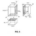
- FIG. 5illustrates crystal lattices for a bulk silicon, a strained silicon germanium semiconductor body and a stained silicon capping layer.
- Embodiments of the present inventionare bulk nonplanar transistors having strained enhanced mobility and their methods of fabrication.
- numerous specific detailshave been set forth in order to provide a thorough understanding of the present invention.
- well known semiconductor processing and fabrication techniqueshave not been set forth in particular detail in order to not unnecessarily obscure the present invention.
- Embodiments of the present inventionare bulk nonplanar transistors having strained enhanced mobility and their methods of fabrication.
- Embodiments of the present inventioninclude a semiconductor body which places a capping layer formed on or around the semiconductor body under strain.
- a capping layer under strainincreases the mobility of carriers in the device which increases the current of the device which can be used to improve circuit speeds.
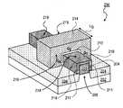
- Transistor 200is formed on a bulk semiconductor substrate 202 .
- the substrate 202is a monocrystalline silicon substrate.
- Formed in semiconductor substrate 202are a pair of spaced apart isolation regions 204 , such as shallow trench isolation (STI) regions, which define the substrate active region 206 therebetween.
- STIshallow trench isolation
- Substrate 202need not necessarily be a silicon monocrystalline substrate and can be other types of substrates, such as but not limited to germanium (Ge), silicon germanium (Si x Ge y ), gallium arsenide (GaAs), InSb, GaP, and GaSb.
- the active region 206is typically doped to a p type conductivity level between 1 ⁇ 10 16 to 1 ⁇ 10 19 atoms/cm 3 for an n type device and doped to an n type conductivity level between 1 ⁇ 10 16 to 1 ⁇ 10 19 atoms/cm 3 for a p type device.
- the active region 206can be an undoped semiconductor, such as an intrinsic or undoped silicon monocrystalline substrate.
- Transistor 200has a semiconductor body 208 formed on active substrate region 206 of bulk substrate 202 .
- the semiconductor body 208has a top surface 209 and a pair of laterally opposite sidewalls 211 .
- the top surface 209is separated from the bottom surface formed on semiconductor substrate 206 by a distance which defines the body height.
- the laterally opposite sidewalls 211 of the semiconductor body 208are separated by a distance which defines the body width.
- the semiconductor body 208is a monocrystalline or single crystalline semiconductor film.
- the semiconductor body 208is formed from a semiconductor material different than the semiconductor used to form the bulk substrate 202 .
- the semiconductor body 208is formed from a single crystalline semiconductor having a different lattice constant or size than the bulk semiconductor substrate 202 so that the semiconductor body 208 is placed under strain.
- the bulk semiconductor substrateis a monocrystalline silicon substrate and the semiconductor body 208 is a single crystalline silicon-germanium alloy.
- the silicon germanium alloycomprises between 5-40% germanium and ideally approximately between 15-25% germanium.
- the bulk semiconductor substrate 202is a monocrystalline silicon substrate and the semiconductor body 208 is a silicon-carbon alloy.
- semiconductor body 208is formed to a thickness less than the amount at which the exterior surfaces of the semiconductor body 208 will cause relaxation in the crystal lattice. In an embodiment of the present invention, semiconductor body 208 is formed to a thickness between 100-2000 ⁇ and more particularly between 200-1000 ⁇ . In an embodiment of the present invention, the thickness and height of the semiconductor body 208 are approximately the same.
- the width of the semiconductor body 208is between half the body 208 height to two times the body 208 height.
- semiconductor body 208is doped to a p type conductivity with a concentration between 1 ⁇ 10 16 to 1 ⁇ 10 19 atoms/cm 3 for an n type semiconductor device and is doped to an n type conductivity with a concentration between 1 ⁇ 10 16 to 1 ⁇ 10 19 atoms/cm 3 for a p type semiconductor device.
- the semiconductor body 208is intrinsic semiconductor, such as an undoped or intrinsic silicon film.
- Transistor 200includes a semiconductor capping layer 210 formed on the sidewalls 211 of semiconductor body 208 as well as on the top surface 209 of semiconductor body 208 .
- Semiconductor capping layer 210is a single crystalline semiconductor film.
- the semiconductor capping layer 210is formed of a semiconductor material having a different lattice constant than the semiconductor body 208 so that a strain is formed in the capping layer.
- the capping layerhas a tensile strain. A tensile strain is thought to improve the mobility of electrons.
- the capping layerhas a compressive strain. A compressive strain is thought to improve hole mobility.
- currentflows in a direction perpendicular to the strain in capping layer 210 .
- the strain in the capping layer 210 on the sidewalls 211 of semiconductor body 208is greater than the strain in the capping layer 210 on the top surface 209 of semiconductor body 208 .
- the semiconductor capping layer 210is a single crystalline silicon film.
- the capping layer 210is a single crystalline silicon film formed on a silicon-germanium alloy body 208 .
- a single crystalline silicon film formed on a silicon-germanium alloy semiconductor body 208will cause the single crystalline silicon film to have a tensile stress.
- the capping layer 210is a single crystalline silicon film formed on a silicon-carbon alloy semiconductor body 208 .
- a single crystalline silicon capping layer 210 formed on a silicon-carbon alloy semiconductor body 208will cause the single crystalline silicon film 210 to have a compressive stress.
- the semiconductor capping layer 210is formed to a thickness less than the amount at which the lattice of the single crystalline film will relax. In an embodiment of the present, the semiconductor capping layer 210 is formed to a thickness between 50-300 ⁇ . In an embodiment of the present invention, the thickness of the capping layer on the sidewalls 211 of semiconductor body 208 is the same as the thickness of the capping layer 210 on the top surface 209 of semiconductor body 208 as illustrated in FIG. 2 . In an embodiment of the present invention, the semiconductor capping layer 210 is formed thicker on the top surface of the semiconductor body 208 than on the sidewalls 211 , such as shown, for example, in FIG. 4C .
- Transistor 200includes a gate dielectric layer 212 .
- Gate dielectric layer 212is formed on capping layer 210 formed on the sidewalls 211 of semiconductor body 208 and is formed on semiconductor capping layer 210 formed on the top surface 209 of semiconductor body 208 .
- Gate dielectric layer 210can be any well known gate dielectric layer.
- the gate dielectric layeris a silicon dioxide (SiO 2 ), silicon oxynitride (SiO x N y ), or a silicon nitride (Si 3 N 4 ) dielectric layer.
- the gate dielectric layer 212is a silicon oxynitride film formed to a thickness between 5-20 ⁇ .
- the gate dielectric layer 212is a high K gate dielectric layer, such as a metal oxide dielectric, such as but not limited to tantalum pentaoxide (Ta 2 O 5 ), titanium oxide (TiO 2 ), hafnium oxide (HfO) and zirconium oxide (ZrO).
- a metal oxide dielectricsuch as but not limited to tantalum pentaoxide (Ta 2 O 5 ), titanium oxide (TiO 2 ), hafnium oxide (HfO) and zirconium oxide (ZrO).
- Gate dielectric layer 212can be other types of high K dielectrics, such as but not limited to PZT and BST.
- Transistor 200includes a gate electrode 214 .
- Gate electrode 214is formed on and around the gate dielectric layer 212 as shown in FIG. 2 .
- Gate electrode 214is formed on and adjacent to gate dielectric layer 212 formed on capping layer 210 formed on sidewall 211 of semiconductor body 208 and is formed on gate dielectric layer 212 formed on capping layer 210 formed on the top surface 209 of semiconductor body 208 and is formed on or adjacent to gate dielectric layer 212 formed on capping layer 210 formed on sidewall 211 of gate electrode 208 as shown in FIG. 2 .
- Gate electrode 214has a pair of laterally opposite sidewalls 216 separated by a distance which defines the gate length (Lg) of transistor 200 .
- gate electrode 214can be formed of any suitable gate electrode material.
- gate electrode 214comprises polycrystalline silicon film doped to a concentration density between 1 ⁇ 10 19 to 1 ⁇ 10 20 atoms/cm 3 .
- Gate electrode 214can be doped to an n type conductivity for an n type device and p type conductivity for a p type device.
- the gate electrodecan be a metal gate electrode.
- the gate electrode 214is formed of a metal film having a work function which is tailored for an n type device, such as a work function between 3.9 eV to 4.2 eV. In an embodiment of the present invention, the gate electrode 214 is formed from a metal film having a work function tailored for a p type device, such as a work function between 4.9 eV to 5.2 eV. In an embodiment of the present invention, the gate electrode 214 is formed from a material having midgap work function between 4.6 to 4.8 eV. A midgap work function is ideal for use when semiconductor body 208 and capping layer 210 are intrinsic semiconductor films. It is to be appreciated that gate electrode 214 need not necessarily be a single material and can be composite stack of thin films, such as but not limited to polycrystalline silicon/metal electrode or metal polycrystalline silicon electrode.
- Transistor 200has a pair source/drain regions formed in semiconductor body 208 as well as in capping layer on opposite sides of a laterally opposite sidewalls 216 of gate electrode 214 as shown in FIG. 2 .
- the source/drain regions 218are doped to an n type conductivity when forming an n type device and doped to a p type conductivity when forming a p type device.
- the source/drain regionshave doping concentration of between 1 ⁇ 10 19 to 1 ⁇ 10 21 atoms/cm 3 .
- the source/drain regions 218can be formed of uniform concentration or can include subregions of different concentrations or doping profiles, such as tip regions (e.g., source/drain extensions).
- transistor 200when transistor 200 is a symmetrical transistor the source and drain regions will have the same doping concentration profile. In an embodiment of the present invention, transistor 200 is an asymmetrical transistor, the source region and drain region may vary in order to obtain particular electrical characteristics.
- the portion of the semiconductor body 208 and capping layer 210 located between the source/drain regions 216 and beneath the gate electrode 214defines a channel region of the transistor.
- the channel regioncan also be defined as the area of semiconductor body 208 and capping layer 210 surrounded by gate electrode 214 .
- the source/drain regionstypically extend slightly beneath the gate electrode through, for example, diffusion to define the channel region slightly smaller than the gate electrode length (Lg).
- Lggate electrode length
- transistor 300When transistor 300 is turned “ON” an inversion layer is formed in the channel region of the device which forms a conductive channel which enables current to travel between the source/drain region 340 .
- the inversion layer or conductive channelforms in the surface of the capping layer on the sidewalls 211 of semiconductor body 208 as well as in the surface of capping layer 210 on the top surface 209 of semiconductor body 208 .
- the nonplanar transistoris characterized as having three channels and three gates, one gate (G 1 ) which extends between the source/drain regions on one side 211 of semiconductor body 208 , a second gate (G 2 ) which extends between the source/drain regions on the top surface 209 of semiconductor body 208 and the third (G 3 ) which extends between the source/drain regions on sidewall 211 of semiconductor body 208 .
- the gate “width” (Gw) of transistor 200is the sum of the width of the three channel regions.
- the gate width of transistor 200is equal to the height of semiconductor body 208 plus the thickness of the capping layer on the top surface of sidewall 211 , plus the width of semiconductor body 208 plus the thickness of the capping layer on each of the sides 211 of semiconductor body plus the height of semiconductor body 208 plus the thickness of capping layer 210 on the top surface 209 of semiconductor body 208 .
- Larger “width” transistorcan be obtained by using multiple semiconductor bodies 208 and capping layers surrounded by a single gate electrode, such as illustrated in FIG. 3I .
- the present inventionis equally applicable to other nonplanar transistors.
- the present inventionis applicable to a “finfet” or a double gate transistor or just two gates are formed on opposite sides of the semiconductor body.
- the present inventionis applicable to “omega” gates or wrap around gate devices where the gate electrode wraps around the semiconductor body as well as underneath a portion of the semiconductor body. Performance of “finfet” devices and “omega” devices can be improved by including a strained capping layer 210 formed on a semiconductor body 208 and thereby enhancing the mobility of carriers in the device.
- a nonplanar deviceis a device which when turned “ON” forms a conductive channel or a portion of the conductive channel in a direction perpendicular to the plane of the substrate 202 .
- a nonplanar transistorcan also be said to be a device where the conductive channel regions are formed both in the horizontal and vertical directions.
- FIGS. 3A-3Iillustrate a method of forming a bulk nonplanar transistor having a strain enhanced mobility in accordance with an embodiment of the present invention.
- semiconductor substrate 300is a monocrystalline silicon substrate.
- Substrate 300need not necessarily be a silicon substrate and can be other types of substrates, such as a silicon germanium substrate, a germanium substrate, a silicon germanium alloy, a gallium arsenide, InSb, and GaP.
- the semiconductor substrate 300is an intrinsic (i.e., undoped) silicon substrate.
- the semiconductor substrate 300is doped to a p type or n type conductivity with a concentration between 1 ⁇ 10 16 to 1 ⁇ 10 19 atom/cm 3 .
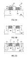
- a mask having mask portions 302 for forming isolation regionsis formed on substrate 300 as shown in FIG. 3A .
- the maskis an oxidation resistant mask.
- the mask portions 302comprise a thin pad oxide layer 304 and a thicker silicon nitride or oxidation resistant layer 306 .
- the mask portions 302define active regions 308 in substrate 300 where transistor bodies are to be formed.
- the mask portions 302can be formed by blanket depositing a pad oxide layer and then a silicon nitride layer over substrate 300 . Next, well known photolithography techniques are used to mask, expose and develop a photoresist masking layer over locations where mask portions 302 are to be formed. The nitride film 306 and the pad oxide layers 304 are then etched in alignment with the formed photoresist mask to form mask portions 302 as shown in FIG. 3A .
- mask portions 302have a width (W 1 ) which is the minimum width or minimum feature dimension (i.e., critical dimension (CD)) which can be defined utilizing photolithography in the fabrication of the transistor. Additionally, in an embodiment of the present invention, mask portions 302 are separated by a distance D 1 which is the minimum distance which can be defined utilizing photolithography in the fabrication process. That is, mask portions 302 have the smallest dimension and are spaced apart by the smallest dimension (i.e., critical dimensions) which can be reliably and achieved utilizing the photolithography process used to fabricate the transistor. In this way, mask portions 302 are defined to have the smallest size and greatest density capable of being achieved with the photolithography process used in fabrication of the transistor.
- W 1is the minimum width or minimum feature dimension (i.e., critical dimension (CD)) which can be defined utilizing photolithography in the fabrication of the transistor.
- D 1is the minimum distance which can be defined utilizing photolithography in the fabrication process. That is, mask portions 302 have the smallest dimension and
- mask portions 302have a thickness (T 1 ) which is equal to or greater than the thickness or height desired for the subsequently formed semiconductor body or bodies.
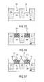
- the exposed portions of semiconductor 300are etched in alignment with the outside edges of mask portion 302 to form trench openings 310 .
- the trench openingsare etched to a depth sufficient to isolate adjacent transistors from one another.
- the trenchesare filled with a dielectric layer 312 to form shallow trench isolation (STI) regions 312 in substrate 300 .
- the dielectric layeris formed by first growing a thin liner oxide in the bottom of sidewalls of trench 310 .
- trench 312is filled by blanket depositing an oxide dielectric layer over the liner oxide by, for example, a high density plasma (HDP) chemical vapor deposition process.
- the fill dielectric layerwill also form on the top of mask portions 302 .
- the fill dielectric layercan then be removed from the top of mask portions 302 by, for example, chemical mechanical polishing.
- the chemical mechanical polishing processis continued until the top surface of mask portions 302 is revealed and the top surface of shallow trench isolation regions 312 substantially planar with the top surface of mask portion 302 as shown in FIG. 3C .
- shallow trench isolation regionsare ideally used in the present invention, other well known isolation regions and techniques, such as local oxidation of silicon (LOCOS) or recessed LOCOS may be utilized.
- LOCOSlocal oxidation of silicon
- recessed LOCOSmay be utilized.
- mask portions 302are removed from substrate 300 to form semiconductor body openings 314 .
- a silicon nitride portion 306is removed utilizing an etchant which etches away the oxidation resistant or silicon nitride portion 306 without significantly etching the isolation regions 312 .
- the pad oxide portion 304is removed.
- Pad oxide portion 304can be removed, for example, with a wet etchant comprising hydrofluoric acid (HF).
- HFhydrofluoric acid
- a semiconductor body film 316is formed in opening 314 as shown in FIG. 3E .
- the semiconductor body film 316is an epitaxial semiconductor film.
- the semiconductor filmwhen a strain enhanced semiconductor device is desired, the semiconductor film is formed from a single crystalline semiconductor film having a different lattice constant or different lattice size than the underlying semiconductor substrate upon which it is grown, so that the semiconductor film is under strain.
- the single crystalline silicon film 316has a larger lattice constant or lattice size than the underlying semiconductor substrate 300 .
- the single crystalline semiconductor film 316has a smaller lattice size or constant than the underlying semiconductor substrate 300 .
- the semiconductor film 316is an epitaxial silicon germanium alloy film selectively grown on a silicon monocrystalline substrate 300 .
- a silicon germanium alloycan be selectively grown in an epitaxial reactor utilizing a deposition gas comprising, dichlorosilane (DCS), H 2 , germane (GeH 4 ), and HCl.
- the silicon germanium alloycomprises between 5-40% germanium and ideally between 15-25% germanium.
- epitaxial semiconductor film 316is a single crystalline silicon carbon alloy formed on a silicon substrate 300 . The single crystalline semiconductor film 316 is deposited to a thickness desired for the thickness of the semiconductor body.
- the isolation regions 312confines the semiconductor film 316 within the trench so that a semiconductor film with nearly vertical sidewalls is formed.
- semiconductor film 316can be blanket deposited over substrate 300 including within trench 314 and on top of isolation regions 312 and then polished back so that the semiconductor film 316 is removed from the top of the isolation regions and remains only within trenches 314 as shown in FIG. 3E .
- the semiconductor film 316is an undoped or intrinsic semiconductor film. In an embodiment of the present invention, when fabricating a p type device, the semiconductor film 316 doped to an n type conductivity with a concentration between 1 ⁇ 10 16 to 1 ⁇ 10 19 atoms/cm 3 . In an embodiment of the present invention, when fabricating an n type device the semiconductor film 316 is doped to a p type conductivity with a concentration between 1 ⁇ 10 16 to 1 ⁇ 10 19 atoms/cm 3 .
- the semiconductor film 316can be doped during deposition in an “insitu” process by including a dopant gas in the deposition process gas mix. Alternatively, the semiconductor film 316 can be subsequently doped by, for example, ion implantation or thermal diffusion to form a doped semiconductor film 316 .
- isolation regions 312are etched back or recessed to expose the sidewalls 320 of semiconductor film 316 and thereby form semiconductor bodies 318 as shown in FIG. 3F .
- Semiconductor bodies 318have nearly vertical sidewalls 320 because semiconductor film 316 was laterally confined by isolation regions 312 during deposition.
- Isolation regions 312are etched back with an etchant which does not significantly etch the semiconductor film 316 .
- semiconductor film 316is a silicon or silicon alloy
- isolation regions 312can be recessed utilizing a wet etchant comprising HF.
- isolation regionsare etched back to a level so that they are substantially planar with the top surface of the active regions 308 formed in semiconductor substrate 300 as shown in FIG. 3F .
- a semiconductor capping layer 322is formed on the top surface 319 and sidewalls 320 of semiconductor body 318 .
- Semiconductor capping layer 322is a single crystalline semiconductor film.
- the semiconductor capping layer 322is formed of a material having a different lattice constant or size than semiconductor body 318 .
- semiconductor capping layer 322is a single crystalline silicon film.
- semiconductor capping layer 322is a single crystalline silicon film formed on a silicon germanium alloy body 318 .
- semiconductor capping layer 322is a single crystalline silicon film formed on a silicon-carbon alloy semiconductor body 318 .
- a single crystalline silicon capping layer 322can be selectively deposited in an epitaxial deposition reactor utilizing a process gas comprising DCS, HCl and H 2 .
- semiconductor capping layer 322is formed to a thickness less than an amount which will cause substantial relaxation in semiconductor capping layer 322 .
- semiconductor capping layer 322is formed to a thickness sufficient to enable the entire inversion layer to be formed in the capping layer when the transistor is turn “ON”.
- semiconductor capping layer 322is formed to a thickness between 50-300 ⁇ .
- semiconductor capping layer 322is an undoped or intrinsic semiconductor film.
- semiconductor capping layer 322is doped to an n type conductivity between 1'10 16 to 1 ⁇ 10 19 atoms/cm 3 when forming a p type device and is doped to a p type conductivity between 1 ⁇ 10 16 to 1 ⁇ 10 19 atoms/cm 3 when forming an n type device.
- semiconductor capping layer 322is doped in an insitu deposition process.
- capping layer 322can be doped by other well known techniques, such as by ion implantation or solid source diffusion.
- gate dielectric layer 324is a grown gate dielectric layer, such as but not limited to a silicon dioxide layer, a silicon oxynitride layer or a combination thereof.
- a silicon oxide or silicon oxynitride layercan be grown on semiconductor capping layer utilizing a well known dry/wet oxidation process. When gate dielectric layer 324 is grown it will form only on semiconductor containing areas, such as capping layer 322 and not on isolation regions 312 .
- gate dielectric layer 324can be a deposited dielectric layer.
- gate dielectric layer 324is a high K gate dielectric layer, such as a metal oxide dielectric layer, such as but not limited to hafnium oxide, zirconium oxide, tantalum oxide and titanium oxide.
- a high K metal oxide dielectric layercan be deposited by any well known technique, such as chemical vapor deposition or sputter deposition. When gate dielectric layer 324 is deposited it will also form on isolation regions 312 .
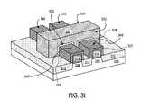
- a gate electrode material 326is blanket deposited over substrate 300 so that it deposits onto and around gate dielectric layer 324 . That is, the gate electrode material is deposited onto the gate dielectric layer 324 formed on capping layer 322 formed on the top surface of semiconductor body 318 and is formed or adjacent to capping layer 322 formed on the sidewalls 320 of semiconductor body 318 .
- the gate electrode material 326is polycrystalline silicon. In an embodiment of the present invention, the gate electrode material 326 is a metal film.
- gate electrode material 326is a metal film having a work function tailored for an n type device and in an embodiment of the present invention, the gate electrode material is metal film having a work function tailored for a p type device. Gate electrode material 326 is formed to a thickness sufficient to completely cover or surround semiconductor bodies 318 , capping layer 322 and gate dielectric layer 324 as shown in FIG. 3H .
- gate electrode material 326 and gate dielectric layer 324are patterned by well known techniques to form a gate electrode 330 and a gate dielectric layer 328 .
- Gate electrode material 326 and gate dielectric layer 324can be patterned utilizing well known photolithography and etching techniques.
- Gate electrode 330has a pair of laterally opposite sidewalls 332 which define the gate length of the device. In an embodiment of the present invention, laterally opposite sidewalls 332 run in a direction perpendicular to semiconductor bodies 318 .
- a subtractive processis shown for the formation of gate electrode 330 , other well known techniques, such as a replacement gate process may be utilized to form gate electrode 330 .
- a pair of source/drain regions 340are formed in capping layer 332 and semiconductor body 318 on opposite sides of gate electrode 330 .
- source/drain regionscan be formed to an n type conductivity with a concentration between 1 ⁇ 10 20 to 1 ⁇ 10 21 atoms/cm 3 .
- source/drain regions having a p type conductivity with a concentration between 1 ⁇ 10 20 to 1 ⁇ 10 21 atoms/cm 3can be formed. Any well known technique, such as ion implantation or thermal diffusion, may be utilized to form the source/drain regions.
- the gate electrode 330can be used to mask the channel region of the transistor from the ion implantation process and thereby self-aligning the source/drain regions 340 with the gate electrode 330 .
- source/drain regionsmay include sub-regions, such as source/drain extensions and source/drain contact regions.
- Well known processes including formation of spacerscan be utilized to form the sub-regions.
- silicidecan be formed on the source/drain regions 340 and on top of the gate electrode 330 to further decrease the electrical contact resistance. This completes the fabrication of bulk nonplanar transistor having strain enhanced mobility.
- back end techniquescan be utilized to form metal contacts, metallization layers and interlayer dielectrics to interconnect various transistors together into functional integrated circuits, such as microprocessors.
- the capping layerincreases the gate width of the transistor.
- minimum feature dimension and spacingcan be used to form the semiconductor bodies and then the capping layer can be formed on and around the minimally defined semiconductor bodies to increase the gate width of the device.
- Thisincreases the current per area of the device which improves device performance.
- Formation of a capping layer on minimally defined and separated featuresreduces the distance between minimally spaced bodies to a distance less than the critical dimension or less than the dimension achievable with photolithography process used to define the device. In this way, the formation of a capping layer enables larger gate width to be achieved with each semiconductor body while still defining the bodies with the minimum critical dimensions (CD) and spacing.
- CDcritical dimensions
- a capping layer to increase the gate widthis valuable even in applications which do not require or desire stress enhanced mobility.
- embodiments of the present inventioninclude applications where, for example, silicon capping layers are formed on minimally spaced silicon bodies in order to increase the gate width of the fabricated transistor.
- use of a capping layer to increase gate width per areais useful in non-bulk devices, such as tri-gate or nonplanar devices formed on insulated substrates, such as in silicon on insulator (SOI) substrates.
- SOIsilicon on insulator
- stacks of semiconductor filmsare engineered to produce high strain in the capping layer 322 which can dramatically increase carrier mobility.
- FIG. 5illustrates how a bulk silicon monocrystalline silicon substrate, a silicon germanium alloy semiconductor body 320 and a silicon capping layer 322 can produce high tensile stress in the silicon capping layer 322 .
- the lattice constant of the plane 502 of the silicon germanium film 318 parallel to the surface of the silicon monocrystalline substrate 300is matched to the silicon lattice of the bulk silicon substrate 300 .
- the lattice constant of the plane 504 of the silicon germanium alloy 316 perpendicular to the silicon substrate surfaceis larger than the plane 502 parallel to the silicon substrate 300 due to the tetragonal distortion of the silicon germanium epitaxial film 316 .
- the isolation regions 312are recessed ( FIG. 3F ) to form silicon germanium body 318 the silicon germanium lattice on the top 319 will expand and the lattice constant on the sides will contract due to the presence of free surface.
- the lattice constant on the sidewall 320 of the silicon germanium alloy 318will be larger than the lattice constant on the top surface 319 of the silicon germanium alloy which will be greater than the lattice constant of the silicon germanium alloy on the silicon monocrystalline substrate.
- the silicon germanium alloy 318When a silicon capping layer 322 is grown on the strained silicon germanium alloy, ( FIG. 3G ) the silicon germanium alloy 318 will impose its lengthened vertical cell dimension 504 on an already smaller cell dimension of the silicon capping layer 322 producing a orthorhombic strained silicon capping layer 322 on the sidewalls of the SiGe body 318 .
- the silicon capping layer formed on the sidewalls 322 of the silicon germanium alloywill witness a substantial tensile strain and a lower but significant tensile strain on the top surface 319 of the silicon germanium alloy.
- the strain produced in silicon capping layer 322is in a direction perpendicular to current flow in the device.
- FIGS. 4A-4Cillustrate a method of forming a bulk nonplanar transistor having strain enhanced mobility wherein the capping layer is formed thicker on the top surface of the semiconductor body than on the sidewalls.
- semiconductor body film 316is grown between isolation regions 312 as described with respect to FIG. 3E .
- a first portion 410 of the capping layeris grown on semiconductor body 316 prior to recessing isolation regions 312 .
- silicon nitride layer 306is formed thicker than necessary for the semiconductor body 318 so that additional room is provided to enable the first portion 410 of the semiconductor capping layer to be grown within the trench 310 .
- the first portion of the capping layer 410can be confined within the isolation regions 312 .
- the isolation regions 312are recessed back as described above to form a semiconductor body 318 having a capping layer 410 formed on the top surface thereof as shown in FIG. 4B .
- a second portion 412 of the capping layeris grown on the sidewalls 320 of the semiconductor body 318 and on the first portion 410 of the capping layer formed on the top surface 319 of semiconductor body 320 .
- the semiconductor capping layer 410is formed to a thickness substantially equal to the thickness of the second portion of the capping layer 412 .
Landscapes
- Insulated Gate Type Field-Effect Transistor (AREA)
- Thin Film Transistor (AREA)
Abstract
Description
- This application is a continuation of U.S. application Ser. No. 11/088,035 filed on Mar. 22, 2005, which is a division of U.S. application Ser. No. 10/816,311 filed on Mar. 31, 2004, now U.S. Pat. No. 7,154,118, the entire contents of which are hereby incorporated by reference herein.
- 1. Field of the Invention
- The present invention relates to the field of integrated circuit manufacturing and more particularly to the formation of a strain enhanced mobility bulk nonplanar transistor and its method of fabrication.
- 2. Discussion of Related Art
- Modern integrated circuits, such as microprocessors, are made up of literally hundreds of millions of transistors coupled together. In order to improve the performance and power of integrated circuits, new transistor structures have been proposed. A nonplanar transistor, such as a tri-gate transistor, has been proposed to improve device performance. A tri-gate
transistor 100 is illustrated inFIGS. 1A and 1B .FIG. 1A is an illustration of a overhead/side view of a tri-gatetransistor 100 andFIG. 1B is an illustration of a cross-sectional view taken through the gate electrode of a tri-gatetransistor 100.Tri-gate transistor 100 includes asilicon body 102 having a pair of laterallyopposite sidewalls 103 and atop surface 104.Silicon body 102 is formed on an insulating substrate including anoxide layer 106 which in turn is formed on amonocrystalline silicon substrate 108. A gate dielectric110 is formed on thetop surface 104 and on thesidewalls 103 ofsilicon body 102. Agate electrode 120 is formed on the gatedielectric layer 110 and surrounds thesilicon body 102. A pair of source/drain regions 130 are formed in thesilicon body 102 along laterally opposite sidewalls ofgate electrode 120.Transistor 130 can be said to be a tri-gate transistor because it essentially has three gates (G1, G2, G3) which essentially form three transistors. Tri-gatetransistor 100 has a first gate/transistor on oneside 103 ofsilicon body 102, a second gate/transistor on atop surface 104 ofsilicon body 102 and a third gate/transistor on thesecond side 103 ofsilicon body 102. Each transistor provides current flow proportional to the sides ofsilicon body 102. The tri-gate transistor are attractive because they have large current per area which improves device performance. FIG. 1A shows an overhead view of a standard tri-gate transistor.FIG. 1B shows a cross-sectional view of standard tri-gate transistor.FIG. 2 is an illustration of a bulk tri-gate transistor having a strain induced mobility in accordance with an embodiment with the present invention.FIGS. 3A-3I illustrate a method of forming a bulk tri-gate transistor having a strain enhanced mobility in accordance with an embodiment of the present invention.FIGS. 4A-4C illustrate a method of forming a bulk tri-gate transistor having a strain enhanced mobility in accordance with an embodiment of the present invention.FIG. 5 illustrates crystal lattices for a bulk silicon, a strained silicon germanium semiconductor body and a stained silicon capping layer.- Embodiments of the present invention are bulk nonplanar transistors having strained enhanced mobility and their methods of fabrication. In the following description, numerous specific details have been set forth in order to provide a thorough understanding of the present invention. In other instances, well known semiconductor processing and fabrication techniques have not been set forth in particular detail in order to not unnecessarily obscure the present invention.
- Embodiments of the present invention are bulk nonplanar transistors having strained enhanced mobility and their methods of fabrication. Embodiments of the present invention include a semiconductor body which places a capping layer formed on or around the semiconductor body under strain. A capping layer under strain increases the mobility of carriers in the device which increases the current of the device which can be used to improve circuit speeds.
- An example of a bulk nonplanar or tri-gate
transistor 200 having strain enhanced mobility is illustrated inFIG. 2 .Transistor 200 is formed on abulk semiconductor substrate 202. In an embodiment of the present invention, thesubstrate 202 is a monocrystalline silicon substrate. Formed insemiconductor substrate 202 are a pair of spacedapart isolation regions 204, such as shallow trench isolation (STI) regions, which define the substrateactive region 206 therebetween.Substrate 202, however, need not necessarily be a silicon monocrystalline substrate and can be other types of substrates, such as but not limited to germanium (Ge), silicon germanium (SixGey), gallium arsenide (GaAs), InSb, GaP, and GaSb. Theactive region 206 is typically doped to a p type conductivity level between 1×10¹⁶to 1×10¹⁹atoms/cm3for an n type device and doped to an n type conductivity level between 1×10¹⁶to 1×10¹⁹atoms/cm3for a p type device. In other embodiments of the present invention, theactive region 206 can be an undoped semiconductor, such as an intrinsic or undoped silicon monocrystalline substrate. Transistor 200 has asemiconductor body 208 formed onactive substrate region 206 ofbulk substrate 202. Thesemiconductor body 208 has atop surface 209 and a pair of laterallyopposite sidewalls 211. Thetop surface 209 is separated from the bottom surface formed onsemiconductor substrate 206 by a distance which defines the body height. The laterallyopposite sidewalls 211 of thesemiconductor body 208 are separated by a distance which defines the body width. Thesemiconductor body 208 is a monocrystalline or single crystalline semiconductor film. In an embodiment of the present invention, thesemiconductor body 208 is formed from a semiconductor material different than the semiconductor used to form thebulk substrate 202. In an embodiment of the present invention, thesemiconductor body 208 is formed from a single crystalline semiconductor having a different lattice constant or size than thebulk semiconductor substrate 202 so that thesemiconductor body 208 is placed under strain. In an embodiment of the present invention, the bulk semiconductor substrate is a monocrystalline silicon substrate and thesemiconductor body 208 is a single crystalline silicon-germanium alloy. In an embodiment of the present invention, the silicon germanium alloy comprises between 5-40% germanium and ideally approximately between 15-25% germanium.- In an embodiment of the present invention, the
bulk semiconductor substrate 202 is a monocrystalline silicon substrate and thesemiconductor body 208 is a silicon-carbon alloy. - In an embodiment of the present invention,
semiconductor body 208 is formed to a thickness less than the amount at which the exterior surfaces of thesemiconductor body 208 will cause relaxation in the crystal lattice. In an embodiment of the present invention,semiconductor body 208 is formed to a thickness between 100-2000 Å and more particularly between 200-1000 Å. In an embodiment of the present invention, the thickness and height of thesemiconductor body 208 are approximately the same. - In an embodiment of the present invention, the width of the
semiconductor body 208 is between half thebody 208 height to two times thebody 208 height. In an embodiment of the present invention,semiconductor body 208 is doped to a p type conductivity with a concentration between 1×10¹⁶to 1×10¹⁹atoms/cm3for an n type semiconductor device and is doped to an n type conductivity with a concentration between 1×10¹⁶to 1×10¹⁹atoms/cm3for a p type semiconductor device. In an embodiment of the present invention, thesemiconductor body 208 is intrinsic semiconductor, such as an undoped or intrinsic silicon film. Transistor 200 includes asemiconductor capping layer 210 formed on thesidewalls 211 ofsemiconductor body 208 as well as on thetop surface 209 ofsemiconductor body 208.Semiconductor capping layer 210 is a single crystalline semiconductor film. In an embodiment of the present invention, thesemiconductor capping layer 210 is formed of a semiconductor material having a different lattice constant than thesemiconductor body 208 so that a strain is formed in the capping layer. In an embodiment of the present invention, the capping layer has a tensile strain. A tensile strain is thought to improve the mobility of electrons. In an embodiment of the present invention, the capping layer has a compressive strain. A compressive strain is thought to improve hole mobility. In an embodiment of the present invention, current flows in a direction perpendicular to the strain in cappinglayer 210. In an embodiment of the present invention, the strain in thecapping layer 210 on thesidewalls 211 ofsemiconductor body 208 is greater than the strain in thecapping layer 210 on thetop surface 209 ofsemiconductor body 208.- In an embodiment of the present invention, the
semiconductor capping layer 210 is a single crystalline silicon film. In an embodiment of the present invention, thecapping layer 210 is a single crystalline silicon film formed on a silicon-germanium alloy body 208. A single crystalline silicon film formed on a silicon-germaniumalloy semiconductor body 208 will cause the single crystalline silicon film to have a tensile stress. In an embodiment of the present invention, thecapping layer 210 is a single crystalline silicon film formed on a silicon-carbonalloy semiconductor body 208. A single crystallinesilicon capping layer 210 formed on a silicon-carbonalloy semiconductor body 208 will cause the singlecrystalline silicon film 210 to have a compressive stress. - In an embodiment of the present invention, the
semiconductor capping layer 210 is formed to a thickness less than the amount at which the lattice of the single crystalline film will relax. In an embodiment of the present, thesemiconductor capping layer 210 is formed to a thickness between 50-300 Å. In an embodiment of the present invention, the thickness of the capping layer on thesidewalls 211 ofsemiconductor body 208 is the same as the thickness of thecapping layer 210 on thetop surface 209 ofsemiconductor body 208 as illustrated inFIG. 2 . In an embodiment of the present invention, thesemiconductor capping layer 210 is formed thicker on the top surface of thesemiconductor body 208 than on thesidewalls 211, such as shown, for example, inFIG. 4C . Transistor 200 includes agate dielectric layer 212.Gate dielectric layer 212 is formed on cappinglayer 210 formed on thesidewalls 211 ofsemiconductor body 208 and is formed onsemiconductor capping layer 210 formed on thetop surface 209 ofsemiconductor body 208.Gate dielectric layer 210 can be any well known gate dielectric layer. In an embodiment of the present invention, the gate dielectric layer is a silicon dioxide (SiO2), silicon oxynitride (SiOxNy), or a silicon nitride (Si3N4) dielectric layer. In an embodiment of the present invention, thegate dielectric layer 212 is a silicon oxynitride film formed to a thickness between 5-20 Å. In an embodiment of the present invention, thegate dielectric layer 212 is a high K gate dielectric layer, such as a metal oxide dielectric, such as but not limited to tantalum pentaoxide (Ta2O5), titanium oxide (TiO2), hafnium oxide (HfO) and zirconium oxide (ZrO).Gate dielectric layer 212, however, can be other types of high K dielectrics, such as but not limited to PZT and BST.Transistor 200 includes agate electrode 214.Gate electrode 214 is formed on and around thegate dielectric layer 212 as shown inFIG. 2 .Gate electrode 214 is formed on and adjacent togate dielectric layer 212 formed on cappinglayer 210 formed onsidewall 211 ofsemiconductor body 208 and is formed ongate dielectric layer 212 formed on cappinglayer 210 formed on thetop surface 209 ofsemiconductor body 208 and is formed on or adjacent togate dielectric layer 212 formed on cappinglayer 210 formed onsidewall 211 ofgate electrode 208 as shown inFIG. 2 .Gate electrode 214 has a pair of laterallyopposite sidewalls 216 separated by a distance which defines the gate length (Lg) oftransistor 200. In an embodiment of the present invention, the laterally oppositesidewalls 216 ofgate electrode 214 run in a direction perpendicular to the laterally oppositesidewalls 211 ofsemiconductor body 208.Gate electrode 214 can be formed of any suitable gate electrode material. In an embodiment of the present invention,gate electrode 214 comprises polycrystalline silicon film doped to a concentration density between 1×10¹⁹to 1×10²⁰atoms/cm3.Gate electrode 214 can be doped to an n type conductivity for an n type device and p type conductivity for a p type device. In an embodiment of the present invention, the gate electrode can be a metal gate electrode. In an embodiment of the present invention, thegate electrode 214 is formed of a metal film having a work function which is tailored for an n type device, such as a work function between 3.9 eV to 4.2 eV. In an embodiment of the present invention, thegate electrode 214 is formed from a metal film having a work function tailored for a p type device, such as a work function between 4.9 eV to 5.2 eV. In an embodiment of the present invention, thegate electrode 214 is formed from a material having midgap work function between 4.6 to 4.8 eV. A midgap work function is ideal for use whensemiconductor body 208 andcapping layer 210 are intrinsic semiconductor films. It is to be appreciated thatgate electrode 214 need not necessarily be a single material and can be composite stack of thin films, such as but not limited to polycrystalline silicon/metal electrode or metal polycrystalline silicon electrode.Transistor 200 has a pair source/drain regions formed insemiconductor body 208 as well as in capping layer on opposite sides of a laterally oppositesidewalls 216 ofgate electrode 214 as shown inFIG. 2 . The source/drain regions 218 are doped to an n type conductivity when forming an n type device and doped to a p type conductivity when forming a p type device. In an embodiment of the present invention, the source/drain regions have doping concentration of between 1×10¹⁹to 1×10²¹atoms/cm3. The source/drain regions 218 can be formed of uniform concentration or can include subregions of different concentrations or doping profiles, such as tip regions (e.g., source/drain extensions). In an embodiment of the present invention, whentransistor 200 is a symmetrical transistor the source and drain regions will have the same doping concentration profile. In an embodiment of the present invention,transistor 200 is an asymmetrical transistor, the source region and drain region may vary in order to obtain particular electrical characteristics.- The portion of the
semiconductor body 208 andcapping layer 210 located between the source/drain regions 216 and beneath thegate electrode 214 defines a channel region of the transistor. The channel region can also be defined as the area ofsemiconductor body 208 andcapping layer 210 surrounded bygate electrode 214. The source/drain regions typically extend slightly beneath the gate electrode through, for example, diffusion to define the channel region slightly smaller than the gate electrode length (Lg). Whentransistor 300 is turned “ON” an inversion layer is formed in the channel region of the device which forms a conductive channel which enables current to travel between the source/drain region 340. The inversion layer or conductive channel forms in the surface of the capping layer on thesidewalls 211 ofsemiconductor body 208 as well as in the surface of cappinglayer 210 on thetop surface 209 ofsemiconductor body 208. - By providing a
gate dielectric layer 212 and agate electrode 214 which surrounds thesemiconductor body 208 andcapping layer 210 on three sides, the nonplanar transistor is characterized as having three channels and three gates, one gate (G1) which extends between the source/drain regions on oneside 211 ofsemiconductor body 208, a second gate (G2) which extends between the source/drain regions on thetop surface 209 ofsemiconductor body 208 and the third (G3) which extends between the source/drain regions onsidewall 211 ofsemiconductor body 208. The gate “width” (Gw) oftransistor 200 is the sum of the width of the three channel regions. That is, the gate width oftransistor 200 is equal to the height ofsemiconductor body 208 plus the thickness of the capping layer on the top surface ofsidewall 211, plus the width ofsemiconductor body 208 plus the thickness of the capping layer on each of thesides 211 of semiconductor body plus the height ofsemiconductor body 208 plus the thickness of cappinglayer 210 on thetop surface 209 ofsemiconductor body 208. Larger “width” transistor can be obtained by usingmultiple semiconductor bodies 208 and capping layers surrounded by a single gate electrode, such as illustrated inFIG. 3I . - Although a
tri-gate transistor 200 is illustrated inFIG. 2 , the present invention is equally applicable to other nonplanar transistors. For example, the present invention is applicable to a “finfet” or a double gate transistor or just two gates are formed on opposite sides of the semiconductor body. Additionally, the present invention, is applicable to “omega” gates or wrap around gate devices where the gate electrode wraps around the semiconductor body as well as underneath a portion of the semiconductor body. Performance of “finfet” devices and “omega” devices can be improved by including astrained capping layer 210 formed on asemiconductor body 208 and thereby enhancing the mobility of carriers in the device. It is to be appreciated that a nonplanar device is a device which when turned “ON” forms a conductive channel or a portion of the conductive channel in a direction perpendicular to the plane of thesubstrate 202. A nonplanar transistor can also be said to be a device where the conductive channel regions are formed both in the horizontal and vertical directions. FIGS. 3A-3I illustrate a method of forming a bulk nonplanar transistor having a strain enhanced mobility in accordance with an embodiment of the present invention. First asemiconductor substrate 300 is provided as shown inFIG. 3A . In an embodiment of the present invention,semiconductor substrate 300 is a monocrystalline silicon substrate.Substrate 300 need not necessarily be a silicon substrate and can be other types of substrates, such as a silicon germanium substrate, a germanium substrate, a silicon germanium alloy, a gallium arsenide, InSb, and GaP. In an embodiment of the present invention, thesemiconductor substrate 300 is an intrinsic (i.e., undoped) silicon substrate. In other embodiments of the present invention, thesemiconductor substrate 300 is doped to a p type or n type conductivity with a concentration between 1×10¹⁶to 1×10¹⁹atom/cm3. Next, a mask havingmask portions 302 for forming isolation regions is formed onsubstrate 300 as shown inFIG. 3A . In an embodiment of the present invention, the mask is an oxidation resistant mask. In an embodiment of the present invention, themask portions 302 comprise a thinpad oxide layer 304 and a thicker silicon nitride or oxidationresistant layer 306. Themask portions 302 defineactive regions 308 insubstrate 300 where transistor bodies are to be formed. Themask portions 302 can be formed by blanket depositing a pad oxide layer and then a silicon nitride layer oversubstrate 300. Next, well known photolithography techniques are used to mask, expose and develop a photoresist masking layer over locations wheremask portions 302 are to be formed. Thenitride film 306 and the pad oxide layers304 are then etched in alignment with the formed photoresist mask to formmask portions 302 as shown inFIG. 3A .- In an embodiment of the present invention,
mask portions 302 have a width (W1) which is the minimum width or minimum feature dimension (i.e., critical dimension (CD)) which can be defined utilizing photolithography in the fabrication of the transistor. Additionally, in an embodiment of the present invention,mask portions 302 are separated by a distance D1 which is the minimum distance which can be defined utilizing photolithography in the fabrication process. That is,mask portions 302 have the smallest dimension and are spaced apart by the smallest dimension (i.e., critical dimensions) which can be reliably and achieved utilizing the photolithography process used to fabricate the transistor. In this way,mask portions 302 are defined to have the smallest size and greatest density capable of being achieved with the photolithography process used in fabrication of the transistor. - In an embodiment of the present invention,
mask portions 302 have a thickness (T1) which is equal to or greater than the thickness or height desired for the subsequently formed semiconductor body or bodies. - Next, as shown in
FIG. 3B , the exposed portions ofsemiconductor 300 are etched in alignment with the outside edges ofmask portion 302 to formtrench openings 310. The trench openings are etched to a depth sufficient to isolate adjacent transistors from one another. - Next, as shown in
FIG. 3C , the trenches are filled with adielectric layer 312 to form shallow trench isolation (STI)regions 312 insubstrate 300. In an embodiment of the present invention, the dielectric layer is formed by first growing a thin liner oxide in the bottom of sidewalls oftrench 310. Next,trench 312 is filled by blanket depositing an oxide dielectric layer over the liner oxide by, for example, a high density plasma (HDP) chemical vapor deposition process. The fill dielectric layer will also form on the top ofmask portions 302. The fill dielectric layer can then be removed from the top ofmask portions 302 by, for example, chemical mechanical polishing. The chemical mechanical polishing process is continued until the top surface ofmask portions 302 is revealed and the top surface of shallowtrench isolation regions 312 substantially planar with the top surface ofmask portion 302 as shown inFIG. 3C . - Although shallow trench isolation regions are ideally used in the present invention, other well known isolation regions and techniques, such as local oxidation of silicon (LOCOS) or recessed LOCOS may be utilized.
- Next, as shown in
FIG. 3D ,mask portions 302 are removed fromsubstrate 300 to formsemiconductor body openings 314. First asilicon nitride portion 306 is removed utilizing an etchant which etches away the oxidation resistant orsilicon nitride portion 306 without significantly etching theisolation regions 312. After removingsilicon nitride portion 306, thepad oxide portion 304 is removed.Pad oxide portion 304 can be removed, for example, with a wet etchant comprising hydrofluoric acid (HF). Removing ofmask portions 302 forms a semiconductor body opening ortrench 314 having substantially vertical sidewalls. The vertical sidewall enables the semiconductor body to be grown within the trench and confined therein to enable a semiconductor body to be formed with nearly vertical sidewalls. - Next, as shown in
FIG. 3E , asemiconductor body film 316 is formed inopening 314 as shown inFIG. 3E . In an embodiment of the present invention, thesemiconductor body film 316 is an epitaxial semiconductor film. In an embodiment of the present invention, when a strain enhanced semiconductor device is desired, the semiconductor film is formed from a single crystalline semiconductor film having a different lattice constant or different lattice size than the underlying semiconductor substrate upon which it is grown, so that the semiconductor film is under strain. In an embodiment of the present invention, the singlecrystalline silicon film 316 has a larger lattice constant or lattice size than theunderlying semiconductor substrate 300. In an embodiment of the present invention, the singlecrystalline semiconductor film 316 has a smaller lattice size or constant than theunderlying semiconductor substrate 300. - In an embodiment of the present invention, the
semiconductor film 316 is an epitaxial silicon germanium alloy film selectively grown on asilicon monocrystalline substrate 300. A silicon germanium alloy can be selectively grown in an epitaxial reactor utilizing a deposition gas comprising, dichlorosilane (DCS), H2, germane (GeH4), and HCl. In an embodiment of the present invention, the silicon germanium alloy comprises between 5-40% germanium and ideally between 15-25% germanium. In an embodiment of the present invention,epitaxial semiconductor film 316 is a single crystalline silicon carbon alloy formed on asilicon substrate 300. The singlecrystalline semiconductor film 316 is deposited to a thickness desired for the thickness of the semiconductor body. In an embodiment of the present invention, it is grown or deposited to a thickness less than the height of the top surface ofisolation regions 312. In this way, theisolation regions 312 confines thesemiconductor film 316 within the trench so that a semiconductor film with nearly vertical sidewalls is formed. Alternatively,semiconductor film 316 can be blanket deposited oversubstrate 300 including withintrench 314 and on top ofisolation regions 312 and then polished back so that thesemiconductor film 316 is removed from the top of the isolation regions and remains only withintrenches 314 as shown inFIG. 3E . - In an embodiment of the present invention, the
semiconductor film 316 is an undoped or intrinsic semiconductor film. In an embodiment of the present invention, when fabricating a p type device, thesemiconductor film 316 doped to an n type conductivity with a concentration between 1×10¹⁶to 1×10¹⁹atoms/cm3. In an embodiment of the present invention, when fabricating an n type device thesemiconductor film 316 is doped to a p type conductivity with a concentration between 1×10¹⁶to 1×10¹⁹atoms/cm3. Thesemiconductor film 316 can be doped during deposition in an “insitu” process by including a dopant gas in the deposition process gas mix. Alternatively, thesemiconductor film 316 can be subsequently doped by, for example, ion implantation or thermal diffusion to form a dopedsemiconductor film 316. - Next,
isolation regions 312 are etched back or recessed to expose thesidewalls 320 ofsemiconductor film 316 and thereby formsemiconductor bodies 318 as shown inFIG. 3F .Semiconductor bodies 318 have nearlyvertical sidewalls 320 becausesemiconductor film 316 was laterally confined byisolation regions 312 during deposition.Isolation regions 312 are etched back with an etchant which does not significantly etch thesemiconductor film 316. Whensemiconductor film 316 is a silicon or siliconalloy isolation regions 312 can be recessed utilizing a wet etchant comprising HF. In an embodiment of the present invention, isolation regions are etched back to a level so that they are substantially planar with the top surface of theactive regions 308 formed insemiconductor substrate 300 as shown inFIG. 3F . - Next, as shown in
FIG. 3G , asemiconductor capping layer 322 is formed on thetop surface 319 andsidewalls 320 ofsemiconductor body 318.Semiconductor capping layer 322 is a single crystalline semiconductor film. In an embodiment of the present invention, thesemiconductor capping layer 322 is formed of a material having a different lattice constant or size thansemiconductor body 318. In an embodiment of the present invention,semiconductor capping layer 322 is a single crystalline silicon film. In an embodiment of the present invention,semiconductor capping layer 322 is a single crystalline silicon film formed on a silicongermanium alloy body 318. In an embodiment of the present invention,semiconductor capping layer 322 is a single crystalline silicon film formed on a silicon-carbonalloy semiconductor body 318. A single crystallinesilicon capping layer 322 can be selectively deposited in an epitaxial deposition reactor utilizing a process gas comprising DCS, HCl and H2. In an embodiment of the present invention,semiconductor capping layer 322 is formed to a thickness less than an amount which will cause substantial relaxation insemiconductor capping layer 322. In an embodiment of the present invention,semiconductor capping layer 322 is formed to a thickness sufficient to enable the entire inversion layer to be formed in the capping layer when the transistor is turn “ON”. In an embodiment of the present invention,semiconductor capping layer 322 is formed to a thickness between 50-300 Å. In an embodiment of the present invention,semiconductor capping layer 322 is an undoped or intrinsic semiconductor film. In an embodiment of the present invention,semiconductor capping layer 322 is doped to an n type conductivity between 1'1016to 1×10¹⁹atoms/cm3when forming a p type device and is doped to a p type conductivity between 1×10¹⁶to 1×10¹⁹atoms/cm3when forming an n type device. In an embodiment of the present invention,semiconductor capping layer 322 is doped in an insitu deposition process. Alternatively, cappinglayer 322 can be doped by other well known techniques, such as by ion implantation or solid source diffusion. - Next, as shown in
FIG. 3H , agate dielectric film 324 is formed on cappinglayer 322 formed on thesidewalls 320 ofsemiconductor body 318 and is formed on thecapping layer 322 formed on thetop surface 319 ofsemiconductor body 318 as shown inFIG. 3H . In an embodiment of the present invention,gate dielectric layer 324 is a grown gate dielectric layer, such as but not limited to a silicon dioxide layer, a silicon oxynitride layer or a combination thereof. A silicon oxide or silicon oxynitride layer can be grown on semiconductor capping layer utilizing a well known dry/wet oxidation process. When gatedielectric layer 324 is grown it will form only on semiconductor containing areas, such ascapping layer 322 and not onisolation regions 312. Alternatively,gate dielectric layer 324 can be a deposited dielectric layer. In an embodiment of the present invention,gate dielectric layer 324 is a high K gate dielectric layer, such as a metal oxide dielectric layer, such as but not limited to hafnium oxide, zirconium oxide, tantalum oxide and titanium oxide. A high K metal oxide dielectric layer can be deposited by any well known technique, such as chemical vapor deposition or sputter deposition. When gatedielectric layer 324 is deposited it will also form onisolation regions 312. - Next, as shown in
FIG. 3H , agate electrode material 326 is blanket deposited oversubstrate 300 so that it deposits onto and aroundgate dielectric layer 324. That is, the gate electrode material is deposited onto thegate dielectric layer 324 formed on cappinglayer 322 formed on the top surface ofsemiconductor body 318 and is formed or adjacent to cappinglayer 322 formed on thesidewalls 320 ofsemiconductor body 318. In an embodiment of the present invention, thegate electrode material 326 is polycrystalline silicon. In an embodiment of the present invention, thegate electrode material 326 is a metal film. In an embodiment of the present invention,gate electrode material 326 is a metal film having a work function tailored for an n type device and in an embodiment of the present invention, the gate electrode material is metal film having a work function tailored for a p type device.Gate electrode material 326 is formed to a thickness sufficient to completely cover or surroundsemiconductor bodies 318, cappinglayer 322 andgate dielectric layer 324 as shown inFIG. 3H . - Next, as shown in
FIG. 3I , thegate electrode material 326 andgate dielectric layer 324 are patterned by well known techniques to form agate electrode 330 and agate dielectric layer 328.Gate electrode material 326 andgate dielectric layer 324 can be patterned utilizing well known photolithography and etching techniques.Gate electrode 330 has a pair of laterallyopposite sidewalls 332 which define the gate length of the device. In an embodiment of the present invention, laterally oppositesidewalls 332 run in a direction perpendicular tosemiconductor bodies 318. Although, a subtractive process is shown for the formation ofgate electrode 330, other well known techniques, such as a replacement gate process may be utilized to formgate electrode 330. - Next, as also shown in
FIG. 3I , a pair of source/drain regions 340 are formed in cappinglayer 332 andsemiconductor body 318 on opposite sides ofgate electrode 330. When forming an n type device, source/drain regions can be formed to an n type conductivity with a concentration between 1×10²⁰to 1×10²¹atoms/cm3. In an embodiment of the present invention, when forming a p type device, source/drain regions having a p type conductivity with a concentration between 1×10²⁰to 1×10²¹atoms/cm3can be formed. Any well known technique, such as ion implantation or thermal diffusion, may be utilized to form the source/drain regions. When ion implantation is used, thegate electrode 330 can be used to mask the channel region of the transistor from the ion implantation process and thereby self-aligning the source/drain regions 340 with thegate electrode 330. Additionally, if desired, source/drain regions may include sub-regions, such as source/drain extensions and source/drain contact regions. Well known processes including formation of spacers can be utilized to form the sub-regions. Additionally, if desired, silicide can be formed on the source/drain regions 340 and on top of thegate electrode 330 to further decrease the electrical contact resistance. This completes the fabrication of bulk nonplanar transistor having strain enhanced mobility. - Well known “back end” techniques can be utilized to form metal contacts, metallization layers and interlayer dielectrics to interconnect various transistors together into functional integrated circuits, such as microprocessors.
- A valuable aspect of the present invention, is that the capping layer increases the gate width of the transistor. In this way, minimum feature dimension and spacing can be used to form the semiconductor bodies and then the capping layer can be formed on and around the minimally defined semiconductor bodies to increase the gate width of the device. This increases the current per area of the device which improves device performance. Formation of a capping layer on minimally defined and separated features reduces the distance between minimally spaced bodies to a distance less than the critical dimension or less than the dimension achievable with photolithography process used to define the device. In this way, the formation of a capping layer enables larger gate width to be achieved with each semiconductor body while still defining the bodies with the minimum critical dimensions (CD) and spacing. Utilizing a capping layer to increase the gate width is valuable even in applications which do not require or desire stress enhanced mobility. As such, embodiments of the present invention include applications where, for example, silicon capping layers are formed on minimally spaced silicon bodies in order to increase the gate width of the fabricated transistor. Additionally, use of a capping layer to increase gate width per area is useful in non-bulk devices, such as tri-gate or nonplanar devices formed on insulated substrates, such as in silicon on insulator (SOI) substrates.
- In embodiments of the present invention, stacks of semiconductor films (i.e.,
bulk semiconductor 300,semiconductor body 318 and capping layer322) are engineered to produce high strain in thecapping layer 322 which can dramatically increase carrier mobility.FIG. 5 illustrates how a bulk silicon monocrystalline silicon substrate, a silicon germaniumalloy semiconductor body 320 and asilicon capping layer 322 can produce high tensile stress in thesilicon capping layer 322. When growing an epitaxial silicongermanium alloy film 316 on a monocrystalline substrate300 (FIG. 3E ) the lattice constant of theplane 502 of thesilicon germanium film 318 parallel to the surface of thesilicon monocrystalline substrate 300 is matched to the silicon lattice of thebulk silicon substrate 300. The lattice constant of theplane 504 of thesilicon germanium alloy 316 perpendicular to the silicon substrate surface is larger than theplane 502 parallel to thesilicon substrate 300 due to the tetragonal distortion of the silicongermanium epitaxial film 316. Once theisolation regions 312 are recessed (FIG. 3F ) to formsilicon germanium body 318 the silicon germanium lattice on the top319 will expand and the lattice constant on the sides will contract due to the presence of free surface. In general the lattice constant on thesidewall 320 of thesilicon germanium alloy 318 will be larger than the lattice constant on thetop surface 319 of the silicon germanium alloy which will be greater than the lattice constant of the silicon germanium alloy on the silicon monocrystalline substrate. When asilicon capping layer 322 is grown on the strained silicon germanium alloy, (FIG. 3G ) thesilicon germanium alloy 318 will impose its lengthenedvertical cell dimension 504 on an already smaller cell dimension of thesilicon capping layer 322 producing a orthorhombic strainedsilicon capping layer 322 on the sidewalls of theSiGe body 318. Thus, the silicon capping layer formed on thesidewalls 322 of the silicon germanium alloy will witness a substantial tensile strain and a lower but significant tensile strain on thetop surface 319 of the silicon germanium alloy. The strain produced insilicon capping layer 322 is in a direction perpendicular to current flow in the device. FIGS. 4A-4C illustrate a method of forming a bulk nonplanar transistor having strain enhanced mobility wherein the capping layer is formed thicker on the top surface of the semiconductor body than on the sidewalls. As illustrated inFIG. 4A ,semiconductor body film 316 is grown betweenisolation regions 312 as described with respect toFIG. 3E . In this embodiment, however, afirst portion 410 of the capping layer is grown onsemiconductor body 316 prior to recessingisolation regions 312. In an embodiment of the present invention,silicon nitride layer 306 is formed thicker than necessary for thesemiconductor body 318 so that additional room is provided to enable thefirst portion 410 of the semiconductor capping layer to be grown within thetrench 310. In this way, the first portion of thecapping layer 410 can be confined within theisolation regions 312. After formation of thefirst portion 410 of the capping layer, theisolation regions 312 are recessed back as described above to form asemiconductor body 318 having acapping layer 410 formed on the top surface thereof as shown inFIG. 4B . Next, as shown inFIG. 4C , asecond portion 412 of the capping layer is grown on thesidewalls 320 of thesemiconductor body 318 and on thefirst portion 410 of the capping layer formed on thetop surface 319 ofsemiconductor body 320. In an embodiment of the present invention, thesemiconductor capping layer 410 is formed to a thickness substantially equal to the thickness of the second portion of thecapping layer 412. In this way, when a substantiallysquare semiconductor body 318 is formed, thesemiconductor body 318 plus capping layer will still provide a substantially square capped body. Next, processing can continue as illustrated inFIGS. 3H and 3I to complete fabrication of the bulk nonplanar transistor having a strain enhanced mobility.
Claims (21)
1. A method of forming a semiconductor device comprising:
forming a pair of isolation regions in a semiconductor substrate, said pair of isolation regions defining an active substrate region in said semiconductor substrate therebetween, said isolation region extending above said substrate;
forming a strained semiconductor film on said active region of said semiconductor substrate between said pair of isolation regions;
etching back said isolation regions to form a strained semiconductor body from said semiconductor film wherein said strained semiconductor body has a top surface and a pair of laterally opposite sidewalls;
forming a semiconductor capping layer on said top surface and said sidewalls of said strained semiconductor body;
forming a gate dielectric layer over said capping layer formed on said sidewalls and of said top surface of said strained semiconductor body;
forming a gate electrode having a pair of laterally opposite sidewalls on and around said gate dielectric layer; and
forming a pair of source/drain regions in said strained semiconductor body on opposite sides of said gate electrode.
2. The method ofclaim 1 , wherein said strained semiconductor film is selectively grown from said active region of said semiconductor substrate with an epitaxial process, wherein the lattice constant of a plane of the strained semiconductor film parallel to the surface of the silicon monocrystalline substrate is matched to the lattice of the semiconductor substrate.
3. The method ofclaim 1 , wherein said semiconductor capping layer on said sidewalls of said strained semiconductor body has a tensile stress exceeding that induced by a lattice constant mismatch between the strained semiconductor film under relaxed conditions and the semiconductor capping layer under relaxed conditions.
4. The method ofclaim 3 , wherein said strained semiconductor body has tetragonal distortion and said semiconductor capping layer has a greater tensile stress on the sidewalls of said strained semiconductor body than on the top surface of said strained semiconductor body.
5. The method ofclaim 1 , wherein said semiconductor capping layer is selectively grown from said strained semiconductor body with an epitaxial process.
6. The method ofclaim 1 , wherein said isolation regions are etched back with a wet etchant.
7. The method ofclaim 5 , wherein said source/drain regions are n type conductivity.
8. The method ofclaim 1 , wherein said semiconductor substrate is a silicon substrate and wherein said strained semiconductor body is a silicon germanium alloy and wherein said semiconductor capping layer is epitaxial silicon.
9. The method ofclaim 1 , wherein said semiconductor capping layer on said sidewalls of said strained semiconductor body has a compressive stress exceeding that induced by a lattice constant mismatch between the strained semiconductor film under relaxed conditions and the semiconductor capping layer under relaxed conditions.
10. The method ofclaim 9 , wherein said strained semiconductor body has tetragonal distortion and said semiconductor capping layer has a greater compressive stress on the sidewalls than on the top surface of said semiconductor body.
11. The method ofclaim 9 , wherein said semiconductor substrate is a monocrystalline silicon substrate, wherein said strained semiconductor body comprises a silicon-carbon alloy and wherein said semiconductor capping layer is epitaxial silicon.
12. The method ofclaim 10 , wherein said source/drain regions are p type conductivity.
13. A semiconductor device comprising:
a strained semiconductor body in contact with a semiconductor substrate layer, said strained semiconductor body having a top surface and laterally opposite sidewalls and said strained semiconductor body having a lattice constant mismatch with the semiconductor substrate layer;
a semiconductor capping layer formed on the top surface and on the sidewalls of said strained semiconductor body, said semiconductor capping layer having a lattice constant mismatch with the strained semiconductor body;
a gate dielectric layer formed on said semiconductor capping layer on said top surface and on said sidewalls of said strained semiconductor body;
a gate electrode having a pair of laterally opposite sidewalls formed on and around said gate dielectric layer; and
a pair of source/drain regions formed in said strained semiconductor body on opposite sides of said gate electrode.
14. The semiconductor device ofclaim 13 , wherein said semiconductor capping layer has a tensile stress.
15. The semiconductor device ofclaim 14 , wherein said strained semiconductor body has tetragonal distortion and said semiconductor capping layer has greater tensile stress on the sidewalls of said strained semiconductor body and then on the top surface of said strained semiconductor body.
15. The semiconductor device ofclaim 14 , wherein said source/drain regions are n type conductivity.
16. The semiconductor device ofclaim 13 , wherein said semiconductor substrate is a silicon substrate, wherein said strained semiconductor body is a silicon germanium alloy and wherein said semiconductor capping layer is a silicon film.
17. The semiconductor device ofclaim 13 , wherein said semiconductor capping layer has a compressive stress.
18. The semiconductor device ofclaim 17 , wherein said strained semiconductor body has tetragonal distortion and said semiconductor capping layer has a greater compressive stress on the sidewalls than on the top surface of said strained semiconductor body.
19. The semiconductor device ofclaim 17 , wherein said semiconductor substrate is a monocrystalline silicon substrate, wherein said strained semiconductor body comprises a silicon-carbon alloy and wherein said semiconductor capping is a single crystalline epitaxial silicon film.
20. The semiconductor device ofclaim 13 , wherein said semiconductor substrate is a silicon substrate, wherein said strained semiconductor body is a silicon germanium epitaxial body, and wherein said semiconductor capping layer is single crystalline epitaxial silicon capping layer.
Priority Applications (1)
| Application Number | Priority Date | Filing Date | Title |
|---|---|---|---|
| US12/025,665US7781771B2 (en) | 2004-03-31 | 2008-02-04 | Bulk non-planar transistor having strained enhanced mobility and methods of fabrication |
Applications Claiming Priority (3)
| Application Number | Priority Date | Filing Date | Title |
|---|---|---|---|
| US10/816,311US7154118B2 (en) | 2004-03-31 | 2004-03-31 | Bulk non-planar transistor having strained enhanced mobility and methods of fabrication |
| US11/088,035US7326634B2 (en) | 2004-03-31 | 2005-03-22 | Bulk non-planar transistor having strained enhanced mobility and methods of fabrication |
| US12/025,665US7781771B2 (en) | 2004-03-31 | 2008-02-04 | Bulk non-planar transistor having strained enhanced mobility and methods of fabrication |
Related Parent Applications (1)
| Application Number | Title | Priority Date | Filing Date |
|---|---|---|---|
| US11/088,035ContinuationUS7326634B2 (en) | 2004-03-31 | 2005-03-22 | Bulk non-planar transistor having strained enhanced mobility and methods of fabrication |
Publications (2)
| Publication Number | Publication Date |
|---|---|
| US20080142841A1true US20080142841A1 (en) | 2008-06-19 |
| US7781771B2 US7781771B2 (en) | 2010-08-24 |
Family
ID=34964024
Family Applications (3)
| Application Number | Title | Priority Date | Filing Date |
|---|---|---|---|
| US10/816,311Expired - LifetimeUS7154118B2 (en) | 2004-03-31 | 2004-03-31 | Bulk non-planar transistor having strained enhanced mobility and methods of fabrication |
| US11/088,035Expired - LifetimeUS7326634B2 (en) | 2004-03-31 | 2005-03-22 | Bulk non-planar transistor having strained enhanced mobility and methods of fabrication |
| US12/025,665Expired - Fee RelatedUS7781771B2 (en) | 2004-03-31 | 2008-02-04 | Bulk non-planar transistor having strained enhanced mobility and methods of fabrication |
Family Applications Before (2)
| Application Number | Title | Priority Date | Filing Date |
|---|---|---|---|
| US10/816,311Expired - LifetimeUS7154118B2 (en) | 2004-03-31 | 2004-03-31 | Bulk non-planar transistor having strained enhanced mobility and methods of fabrication |
| US11/088,035Expired - LifetimeUS7326634B2 (en) | 2004-03-31 | 2005-03-22 | Bulk non-planar transistor having strained enhanced mobility and methods of fabrication |
Country Status (6)
| Country | Link |
|---|---|
| US (3) | US7154118B2 (en) |
| KR (1) | KR100845175B1 (en) |
| CN (1) | CN101189730B (en) |
| DE (1) | DE112005000704B4 (en) |
| TW (1) | TWI269358B (en) |
| WO (1) | WO2005098963A1 (en) |
Cited By (13)
| Publication number | Priority date | Publication date | Assignee | Title |
|---|---|---|---|---|
| US20070262353A1 (en)* | 2006-04-28 | 2007-11-15 | Nobuyasu Nishiyama | Semiconductor device and method of fabricating the same |
| US20110147847A1 (en)* | 2009-12-21 | 2011-06-23 | Cea Stephen M | Methods and apparatus to reduce layout based strain variations in non-planar transistor structures |
| US20110248348A1 (en)* | 2010-04-08 | 2011-10-13 | Taiwan Semiconductor Manufacturing Company, Ltd. | Hybrid Gate Process For Fabricating Finfet Device |
| WO2013095346A1 (en)* | 2011-12-19 | 2013-06-27 | Intel Corporation | Non-planar iii-n transistor |
| US8768271B1 (en) | 2012-12-19 | 2014-07-01 | Intel Corporation | Group III-N transistors on nanoscale template structures |
| WO2014209509A1 (en)* | 2013-06-24 | 2014-12-31 | International Business Machines Corporation | Semiconductor device including source/drain formed on bulk and gate channel formed on oxide layer |
| TWI567980B (en)* | 2015-07-20 | 2017-01-21 | 台灣積體電路製造股份有限公司 | Method and structure for fin field effect transistor elements |
| US20170236826A1 (en)* | 2013-04-04 | 2017-08-17 | Stmicroelectronics, Inc. | Integrated circuit devices and fabrication techniques |
| US9847392B1 (en)* | 2016-10-11 | 2017-12-19 | United Microelectronics Corp. | Semiconductor device and method for fabricating the same |
| TWI647823B (en)* | 2016-11-09 | 2019-01-11 | 大陸商上海新昇半導體科技有限公司 | Complementary transistor element structure and manufacturing method thereof |
| US10714477B2 (en) | 2016-08-11 | 2020-07-14 | Gachon University Of Industry-Academic Cooperation Foundation | SiGe p-channel tri-gate transistor based on bulk silicon and fabrication method thereof |
| US11004954B2 (en)* | 2016-09-30 | 2021-05-11 | Intel Corporation | Epitaxial buffer to reduce sub-channel leakage in MOS transistors |
| US11081570B2 (en)* | 2016-09-28 | 2021-08-03 | Intel Corporation | Transistors with lattice matched gate structure |
Families Citing this family (260)
| Publication number | Priority date | Publication date | Assignee | Title |
|---|---|---|---|---|
| US7358121B2 (en)* | 2002-08-23 | 2008-04-15 | Intel Corporation | Tri-gate devices and methods of fabrication |
| US7074656B2 (en)* | 2003-04-29 | 2006-07-11 | Taiwan Semiconductor Manufacturing Company, Ltd. | Doping of semiconductor fin devices |
| CN1799146A (en)* | 2003-05-30 | 2006-07-05 | 松下电器产业株式会社 | Semiconductor device and method for manufacturing same |
| US20070020833A1 (en)* | 2003-06-26 | 2007-01-25 | Rj Mears, Llc | Method for Making a Semiconductor Device Including a Channel with a Non-Semiconductor Layer Monolayer |
| US7612366B2 (en)* | 2003-06-26 | 2009-11-03 | Mears Technologies, Inc. | Semiconductor device including a strained superlattice layer above a stress layer |
| US20070010040A1 (en)* | 2003-06-26 | 2007-01-11 | Rj Mears, Llc | Method for Making a Semiconductor Device Including a Strained Superlattice Layer Above a Stress Layer |
| US7531828B2 (en)* | 2003-06-26 | 2009-05-12 | Mears Technologies, Inc. | Semiconductor device including a strained superlattice between at least one pair of spaced apart stress regions |
| US7598515B2 (en)* | 2003-06-26 | 2009-10-06 | Mears Technologies, Inc. | Semiconductor device including a strained superlattice and overlying stress layer and related methods |
| US20070015344A1 (en)* | 2003-06-26 | 2007-01-18 | Rj Mears, Llc | Method for Making a Semiconductor Device Including a Strained Superlattice Between at Least One Pair of Spaced Apart Stress Regions |
| US20070020860A1 (en)* | 2003-06-26 | 2007-01-25 | Rj Mears, Llc | Method for Making Semiconductor Device Including a Strained Superlattice and Overlying Stress Layer and Related Methods |
| US6909151B2 (en) | 2003-06-27 | 2005-06-21 | Intel Corporation | Nonplanar device with stress incorporation layer and method of fabrication |
| US7456476B2 (en) | 2003-06-27 | 2008-11-25 | Intel Corporation | Nonplanar semiconductor device with partially or fully wrapped around gate electrode and methods of fabrication |
| US7105390B2 (en) | 2003-12-30 | 2006-09-12 | Intel Corporation | Nonplanar transistors with metal gate electrodes |
| US7268058B2 (en) | 2004-01-16 | 2007-09-11 | Intel Corporation | Tri-gate transistors and methods to fabricate same |
| US7154118B2 (en) | 2004-03-31 | 2006-12-26 | Intel Corporation | Bulk non-planar transistor having strained enhanced mobility and methods of fabrication |
| US7579280B2 (en) | 2004-06-01 | 2009-08-25 | Intel Corporation | Method of patterning a film |
| KR100541657B1 (en)* | 2004-06-29 | 2006-01-11 | 삼성전자주식회사 | Multi-gate transistor fabrication method and multi-gate transistor fabricated thereby |
| US7042009B2 (en) | 2004-06-30 | 2006-05-09 | Intel Corporation | High mobility tri-gate devices and methods of fabrication |
| US7598134B2 (en)* | 2004-07-28 | 2009-10-06 | Micron Technology, Inc. | Memory device forming methods |
| US7348284B2 (en) | 2004-08-10 | 2008-03-25 | Intel Corporation | Non-planar pMOS structure with a strained channel region and an integrated strained CMOS flow |
| US7253493B2 (en)* | 2004-08-24 | 2007-08-07 | Micron Technology, Inc. | High density access transistor having increased channel width and methods of fabricating such devices |
| US7679145B2 (en)* | 2004-08-31 | 2010-03-16 | Intel Corporation | Transistor performance enhancement using engineered strains |
| US8673706B2 (en)* | 2004-09-01 | 2014-03-18 | Micron Technology, Inc. | Methods of forming layers comprising epitaxial silicon |
| US7531395B2 (en)* | 2004-09-01 | 2009-05-12 | Micron Technology, Inc. | Methods of forming a layer comprising epitaxial silicon, and methods of forming field effect transistors |
| US7132355B2 (en)* | 2004-09-01 | 2006-11-07 | Micron Technology, Inc. | Method of forming a layer comprising epitaxial silicon and a field effect transistor |
| US7144779B2 (en)* | 2004-09-01 | 2006-12-05 | Micron Technology, Inc. | Method of forming epitaxial silicon-comprising material |
| US7422946B2 (en) | 2004-09-29 | 2008-09-09 | Intel Corporation | Independently accessed double-gate and tri-gate transistors in same process flow |
| US7332439B2 (en) | 2004-09-29 | 2008-02-19 | Intel Corporation | Metal gate transistors with epitaxial source and drain regions |
| US7361958B2 (en) | 2004-09-30 | 2008-04-22 | Intel Corporation | Nonplanar transistors with metal gate electrodes |
| US20060086977A1 (en) | 2004-10-25 | 2006-04-27 | Uday Shah | Nonplanar device with thinned lower body portion and method of fabrication |
| US7393733B2 (en)* | 2004-12-01 | 2008-07-01 | Amberwave Systems Corporation | Methods of forming hybrid fin field-effect transistor structures |
| US7235501B2 (en) | 2004-12-13 | 2007-06-26 | Micron Technology, Inc. | Lanthanum hafnium oxide dielectrics |
| US7193279B2 (en)* | 2005-01-18 | 2007-03-20 | Intel Corporation | Non-planar MOS structure with a strained channel region |
| FR2881877B1 (en)* | 2005-02-04 | 2007-08-31 | Soitec Silicon On Insulator | MULTI-LAYER CHANNEL FIELD EFFECT TRANSISTOR WITH MULTI-LAYER CHANNEL |
| US7518196B2 (en) | 2005-02-23 | 2009-04-14 | Intel Corporation | Field effect transistor with narrow bandgap source and drain regions and method of fabrication |
| US20060202266A1 (en) | 2005-03-14 | 2006-09-14 | Marko Radosavljevic | Field effect transistor with metal source/drain regions |
| US20060214233A1 (en)* | 2005-03-22 | 2006-09-28 | Ananthanarayanan Hari P | FinFET semiconductor device |
| FR2885733B1 (en)* | 2005-05-16 | 2008-03-07 | St Microelectronics Crolles 2 | THREE-GRID TRANSISTOR STRUCTURE |
| US9153645B2 (en) | 2005-05-17 | 2015-10-06 | Taiwan Semiconductor Manufacturing Company, Ltd. | Lattice-mismatched semiconductor structures with reduced dislocation defect densities and related methods for device fabrication |
| US8324660B2 (en) | 2005-05-17 | 2012-12-04 | Taiwan Semiconductor Manufacturing Company, Ltd. | Lattice-mismatched semiconductor structures with reduced dislocation defect densities and related methods for device fabrication |
| US7858481B2 (en) | 2005-06-15 | 2010-12-28 | Intel Corporation | Method for fabricating transistor with thinned channel |
| US7547637B2 (en) | 2005-06-21 | 2009-06-16 | Intel Corporation | Methods for patterning a semiconductor film |
| US20060286759A1 (en)* | 2005-06-21 | 2006-12-21 | Texas Instruments, Inc. | Metal oxide semiconductor (MOS) device having both an accumulation and a enhancement mode transistor device on a similar substrate and a method of manufacture therefor |
| US7279375B2 (en) | 2005-06-30 | 2007-10-09 | Intel Corporation | Block contact architectures for nanoscale channel transistors |
| US7265008B2 (en) | 2005-07-01 | 2007-09-04 | Synopsys, Inc. | Method of IC production using corrugated substrate |
| US7190050B2 (en)* | 2005-07-01 | 2007-03-13 | Synopsys, Inc. | Integrated circuit on corrugated substrate |
| US7247887B2 (en)* | 2005-07-01 | 2007-07-24 | Synopsys, Inc. | Segmented channel MOS transistor |
| KR101329388B1 (en) | 2005-07-26 | 2013-11-14 | 앰버웨이브 시스템즈 코포레이션 | Solutions for integrated circuit integration of alternative active area materials |
| US7288802B2 (en)* | 2005-07-27 | 2007-10-30 | International Business Machines Corporation | Virtual body-contacted trigate |
| US7381649B2 (en)* | 2005-07-29 | 2008-06-03 | Taiwan Semiconductor Manufacturing Company, Ltd. | Structure for a multiple-gate FET device and a method for its fabrication |
| US7348642B2 (en) | 2005-08-03 | 2008-03-25 | International Business Machines Corporation | Fin-type field effect transistor |
| US7402875B2 (en) | 2005-08-17 | 2008-07-22 | Intel Corporation | Lateral undercut of metal gate in SOI device |
| US7479421B2 (en) | 2005-09-28 | 2009-01-20 | Intel Corporation | Process for integrating planar and non-planar CMOS transistors on a bulk substrate and article made thereby |
| US20070090416A1 (en) | 2005-09-28 | 2007-04-26 | Doyle Brian S | CMOS devices with a single work function gate electrode and method of fabrication |
| US20070102756A1 (en)* | 2005-11-10 | 2007-05-10 | Bohumil Lojek | FinFET transistor fabricated in bulk semiconducting material |
| DE102006027178A1 (en)* | 2005-11-21 | 2007-07-05 | Infineon Technologies Ag | A multi-fin device array and method of fabricating a multi-fin device array |
| US7485503B2 (en) | 2005-11-30 | 2009-02-03 | Intel Corporation | Dielectric interface for group III-V semiconductor device |
| US8183556B2 (en) | 2005-12-15 | 2012-05-22 | Intel Corporation | Extreme high mobility CMOS logic |
| KR100713924B1 (en)* | 2005-12-23 | 2007-05-07 | 주식회사 하이닉스반도체 | Protruding transistor and method of forming the same |
| US7525160B2 (en)* | 2005-12-27 | 2009-04-28 | Intel Corporation | Multigate device with recessed strain regions |
| US7396711B2 (en) | 2005-12-27 | 2008-07-08 | Intel Corporation | Method of fabricating a multi-cornered film |
| US20070161214A1 (en) | 2006-01-06 | 2007-07-12 | International Business Machines Corporation | High k gate stack on III-V compound semiconductors |
| DE102006001680B3 (en) | 2006-01-12 | 2007-08-09 | Infineon Technologies Ag | Manufacturing method for a FinFET transistor arrangement and corresponding FinFET transistor arrangement |
| US7709402B2 (en) | 2006-02-16 | 2010-05-04 | Micron Technology, Inc. | Conductive layers for hafnium silicon oxynitride films |
| WO2007112066A2 (en) | 2006-03-24 | 2007-10-04 | Amberwave Systems Corporation | Lattice-mismatched semiconductor structures and related methods for device fabrication |
| US7449373B2 (en) | 2006-03-31 | 2008-11-11 | Intel Corporation | Method of ion implanting for tri-gate devices |
| WO2007133775A2 (en) | 2006-05-15 | 2007-11-22 | Carnegie Mellon University | Integrated circuit, device, system, and method of fabrication |
| US7422960B2 (en) | 2006-05-17 | 2008-09-09 | Micron Technology, Inc. | Method of forming gate arrays on a partial SOI substrate |
| JP2007329200A (en)* | 2006-06-06 | 2007-12-20 | Toshiba Corp | Manufacturing method of semiconductor device |
| JP4552908B2 (en)* | 2006-07-26 | 2010-09-29 | エルピーダメモリ株式会社 | Manufacturing method of semiconductor device |
| US8143646B2 (en) | 2006-08-02 | 2012-03-27 | Intel Corporation | Stacking fault and twin blocking barrier for integrating III-V on Si |
| US7727908B2 (en) | 2006-08-03 | 2010-06-01 | Micron Technology, Inc. | Deposition of ZrA1ON films |
| US7537994B2 (en) | 2006-08-28 | 2009-05-26 | Micron Technology, Inc. | Methods of forming semiconductor devices, assemblies and constructions |
| US7759747B2 (en) | 2006-08-31 | 2010-07-20 | Micron Technology, Inc. | Tantalum aluminum oxynitride high-κ dielectric |
| US7776765B2 (en) | 2006-08-31 | 2010-08-17 | Micron Technology, Inc. | Tantalum silicon oxynitride high-k dielectrics and metal gates |
| US8173551B2 (en) | 2006-09-07 | 2012-05-08 | Taiwan Semiconductor Manufacturing Co., Ltd. | Defect reduction using aspect ratio trapping |
| US7456471B2 (en)* | 2006-09-15 | 2008-11-25 | International Business Machines Corporation | Field effect transistor with raised source/drain fin straps |
| WO2008039534A2 (en) | 2006-09-27 | 2008-04-03 | Amberwave Systems Corporation | Quantum tunneling devices and circuits with lattice- mismatched semiconductor structures |
| WO2008039495A1 (en)* | 2006-09-27 | 2008-04-03 | Amberwave Systems Corporation | Tri-gate field-effect transistors formed by aspect ratio trapping |
| US8502263B2 (en) | 2006-10-19 | 2013-08-06 | Taiwan Semiconductor Manufacturing Company, Ltd. | Light-emitter-based devices with lattice-mismatched semiconductor structures |
| US7829407B2 (en)* | 2006-11-20 | 2010-11-09 | International Business Machines Corporation | Method of fabricating a stressed MOSFET by bending SOI region |
| US7728364B2 (en)* | 2007-01-19 | 2010-06-01 | International Business Machines Corporation | Enhanced mobility CMOS transistors with a V-shaped channel with self-alignment to shallow trench isolation |
| US8735990B2 (en)* | 2007-02-28 | 2014-05-27 | International Business Machines Corporation | Radiation hardened FinFET |
| JP5003515B2 (en)* | 2007-03-20 | 2012-08-15 | ソニー株式会社 | Semiconductor device |
| US8237151B2 (en) | 2009-01-09 | 2012-08-07 | Taiwan Semiconductor Manufacturing Company, Ltd. | Diode-based devices and methods for making the same |
| US7825328B2 (en) | 2007-04-09 | 2010-11-02 | Taiwan Semiconductor Manufacturing Company, Ltd. | Nitride-based multi-junction solar cell modules and methods for making the same |
| US8304805B2 (en) | 2009-01-09 | 2012-11-06 | Taiwan Semiconductor Manufacturing Company, Ltd. | Semiconductor diodes fabricated by aspect ratio trapping with coalesced films |
| WO2008124154A2 (en) | 2007-04-09 | 2008-10-16 | Amberwave Systems Corporation | Photovoltaics on silicon |
| US8927353B2 (en) | 2007-05-07 | 2015-01-06 | Taiwan Semiconductor Manufacturing Co., Ltd. | Fin field effect transistor and method of forming the same |
| US8450165B2 (en) | 2007-05-14 | 2013-05-28 | Intel Corporation | Semiconductor device having tipless epitaxial source/drain regions |
| US20080293192A1 (en)* | 2007-05-22 | 2008-11-27 | Stefan Zollner | Semiconductor device with stressors and methods thereof |
| US8174073B2 (en)* | 2007-05-30 | 2012-05-08 | Taiwan Semiconductor Manufacturing Co., Ltd. | Integrated circuit structures with multiple FinFETs |
| US8329541B2 (en) | 2007-06-15 | 2012-12-11 | Taiwan Semiconductor Manufacturing Company, Ltd. | InP-based transistor fabrication |
| US20090001415A1 (en)* | 2007-06-30 | 2009-01-01 | Nick Lindert | Multi-gate transistor with strained body |
| US7692254B2 (en)* | 2007-07-16 | 2010-04-06 | International Business Machines Corporation | Fin-type field effect transistor structure with merged source/drain silicide and method of forming the structure |
| US7969808B2 (en)* | 2007-07-20 | 2011-06-28 | Samsung Electronics Co., Ltd. | Memory cell structures, memory arrays, memory devices, memory controllers, and memory systems, and methods of manufacturing and operating the same |
| KR20090116088A (en)* | 2008-05-06 | 2009-11-11 | 삼성전자주식회사 | Capacitorless 1T Semiconductor Memory Devices with Improved Information Retention and Operational Characteristics |
| JP2010538495A (en) | 2007-09-07 | 2010-12-09 | アンバーウェーブ・システムズ・コーポレーション | Multi-junction solar cell |
| KR101308048B1 (en)* | 2007-10-10 | 2013-09-12 | 삼성전자주식회사 | Semiconductor memory device |
| KR20090075063A (en)* | 2008-01-03 | 2009-07-08 | 삼성전자주식회사 | A semiconductor memory device having a memory cell array having a dynamic memory cell using a floating body transistor and a method of operating the device |
| US7982269B2 (en)* | 2008-04-17 | 2011-07-19 | International Business Machines Corporation | Transistors having asymmetric strained source/drain portions |
| JP5159413B2 (en)* | 2008-04-24 | 2013-03-06 | 株式会社東芝 | Semiconductor device and manufacturing method thereof |
| US8183667B2 (en) | 2008-06-03 | 2012-05-22 | Taiwan Semiconductor Manufacturing Co., Ltd. | Epitaxial growth of crystalline material |
| US8362566B2 (en) | 2008-06-23 | 2013-01-29 | Intel Corporation | Stress in trigate devices using complimentary gate fill materials |
| US8274097B2 (en) | 2008-07-01 | 2012-09-25 | Taiwan Semiconductor Manufacturing Company, Ltd. | Reduction of edge effects from aspect ratio trapping |
| US8981427B2 (en) | 2008-07-15 | 2015-03-17 | Taiwan Semiconductor Manufacturing Company, Ltd. | Polishing of small composite semiconductor materials |
| US7833891B2 (en)* | 2008-07-23 | 2010-11-16 | International Business Machines Corporation | Semiconductor device manufacturing method using oxygen diffusion barrier layer between buried oxide layer and high K dielectric layer |
| EP2335273A4 (en) | 2008-09-19 | 2012-01-25 | Taiwan Semiconductor Mfg | FORMATION OF DEVICES BY GROWTH OF EPITAXIAL LAYERS |
| US20100072515A1 (en) | 2008-09-19 | 2010-03-25 | Amberwave Systems Corporation | Fabrication and structures of crystalline material |
| US8253211B2 (en) | 2008-09-24 | 2012-08-28 | Taiwan Semiconductor Manufacturing Company, Ltd. | Semiconductor sensor structures with reduced dislocation defect densities |
| KR20100070158A (en)* | 2008-12-17 | 2010-06-25 | 삼성전자주식회사 | Semiconductor memory device comprising capacitor-less dynamic memory cells, and method of operating the same |
| KR101442177B1 (en)* | 2008-12-18 | 2014-09-18 | 삼성전자주식회사 | Processes for fabricating semiconductor devices with capacitorless one-transistor memory cells |
| US8058692B2 (en) | 2008-12-29 | 2011-11-15 | Taiwan Semiconductor Manufacturing Company, Ltd. | Multiple-gate transistors with reverse T-shaped fins |
| US8305829B2 (en)* | 2009-02-23 | 2012-11-06 | Taiwan Semiconductor Manufacturing Company, Ltd. | Memory power gating circuit for controlling internal voltage of a memory array, system and method for controlling the same |
| US8305790B2 (en)* | 2009-03-16 | 2012-11-06 | Taiwan Semiconductor Manufacturing Company, Ltd. | Electrical anti-fuse and related applications |
| US8957482B2 (en)* | 2009-03-31 | 2015-02-17 | Taiwan Semiconductor Manufacturing Company, Ltd. | Electrical fuse and related applications |
| CN101853882B (en) | 2009-04-01 | 2016-03-23 | 台湾积体电路制造股份有限公司 | There is the high-mobility multiple-gate transistor of the switch current ratio of improvement |
| US8816391B2 (en)* | 2009-04-01 | 2014-08-26 | Taiwan Semiconductor Manufacturing Company, Ltd. | Source/drain engineering of devices with high-mobility channels |
| US8629446B2 (en) | 2009-04-02 | 2014-01-14 | Taiwan Semiconductor Manufacturing Company, Ltd. | Devices formed from a non-polar plane of a crystalline material and method of making the same |
| US8912602B2 (en)* | 2009-04-14 | 2014-12-16 | Taiwan Semiconductor Manufacturing Company, Ltd. | FinFETs and methods for forming the same |
| US8455860B2 (en) | 2009-04-30 | 2013-06-04 | Taiwan Semiconductor Manufacturing Company, Ltd. | Reducing source/drain resistance of III-V based transistors |
| US9768305B2 (en) | 2009-05-29 | 2017-09-19 | Taiwan Semiconductor Manufacturing Company, Ltd. | Gradient ternary or quaternary multiple-gate transistor |
| US8617976B2 (en) | 2009-06-01 | 2013-12-31 | Taiwan Semiconductor Manufacturing Company, Ltd. | Source/drain re-growth for manufacturing III-V based transistors |
| US8461015B2 (en)* | 2009-07-08 | 2013-06-11 | Taiwan Semiconductor Manufacturing Company, Ltd. | STI structure and method of forming bottom void in same |
| US8264021B2 (en)* | 2009-10-01 | 2012-09-11 | Taiwan Semiconductor Manufacturing Company, Ltd. | Finfets and methods for forming the same |
| US8264032B2 (en)* | 2009-09-01 | 2012-09-11 | Taiwan Semiconductor Manufacturing Company, Ltd. | Accumulation type FinFET, circuits and fabrication method thereof |
| US8629478B2 (en)* | 2009-07-31 | 2014-01-14 | Taiwan Semiconductor Manufacturing Company, Ltd. | Fin structure for high mobility multiple-gate transistor |
| US9484462B2 (en)* | 2009-09-24 | 2016-11-01 | Taiwan Semiconductor Manufacturing Company, Ltd. | Fin structure of fin field effect transistor |
| US8623728B2 (en)* | 2009-07-28 | 2014-01-07 | Taiwan Semiconductor Manufacturing Company, Ltd. | Method for forming high germanium concentration SiGe stressor |
| US8298925B2 (en) | 2010-11-08 | 2012-10-30 | Taiwan Semiconductor Manufacturing Company, Ltd. | Mechanisms for forming ultra shallow junction |
| US8980719B2 (en) | 2010-04-28 | 2015-03-17 | Taiwan Semiconductor Manufacturing Company, Ltd. | Methods for doping fin field-effect transistors |
| US8759943B2 (en) | 2010-10-08 | 2014-06-24 | Taiwan Semiconductor Manufacturing Company, Ltd. | Transistor having notched fin structure and method of making the same |
| US8440517B2 (en) | 2010-10-13 | 2013-05-14 | Taiwan Semiconductor Manufacturing Company, Ltd. | FinFET and method of fabricating the same |
| US8482073B2 (en)* | 2010-03-25 | 2013-07-09 | Taiwan Semiconductor Manufacturing Company, Ltd. | Integrated circuit including FINFETs and methods for forming the same |
| US8497528B2 (en) | 2010-05-06 | 2013-07-30 | Taiwan Semiconductor Manufacturing Company, Ltd. | Method for fabricating a strained structure |
| US8472227B2 (en)* | 2010-01-27 | 2013-06-25 | Taiwan Semiconductor Manufacturing Company, Ltd. | Integrated circuits and methods for forming the same |
| US20110097867A1 (en)* | 2009-10-22 | 2011-04-28 | Taiwan Semiconductor Manufacturing Company, Ltd. | Method of controlling gate thicknesses in forming fusi gates |
| EP2315239A1 (en)* | 2009-10-23 | 2011-04-27 | Imec | A method of forming monocrystalline germanium or silicon germanium |
| US9040393B2 (en) | 2010-01-14 | 2015-05-26 | Taiwan Semiconductor Manufacturing Company, Ltd. | Method of forming semiconductor structure |
| JP5166458B2 (en)* | 2010-01-22 | 2013-03-21 | 株式会社東芝 | Semiconductor device and manufacturing method thereof |
| US8207038B2 (en) | 2010-05-24 | 2012-06-26 | International Business Machines Corporation | Stressed Fin-FET devices with low contact resistance |
| DE102010038742B4 (en)* | 2010-07-30 | 2016-01-21 | Globalfoundries Dresden Module One Llc & Co. Kg | Method and semiconductor device based on a deformation technology in three-dimensional transistors based on a deformed channel semiconductor material |
| US8603924B2 (en) | 2010-10-19 | 2013-12-10 | Taiwan Semiconductor Manufacturing Company, Ltd. | Methods of forming gate dielectric material |
| US9048181B2 (en) | 2010-11-08 | 2015-06-02 | Taiwan Semiconductor Manufacturing Company, Ltd. | Mechanisms for forming ultra shallow junction |
| US8769446B2 (en) | 2010-11-12 | 2014-07-01 | Taiwan Semiconductor Manufacturing Company, Ltd. | Method and device for increasing fin device density for unaligned fins |
| US8936978B2 (en)* | 2010-11-29 | 2015-01-20 | International Business Machines Corporation | Multigate structure formed with electroless metal deposition |
| US8592915B2 (en) | 2011-01-25 | 2013-11-26 | Taiwan Semiconductor Manufacturing Company, Ltd. | Doped oxide for shallow trench isolation (STI) |
| US8877602B2 (en) | 2011-01-25 | 2014-11-04 | Taiwan Semiconductor Manufacturing Company, Ltd. | Mechanisms of doping oxide for forming shallow trench isolation |
| US8431453B2 (en) | 2011-03-31 | 2013-04-30 | Taiwan Semiconductor Manufacturing Company, Ltd. | Plasma doping to reduce dielectric loss during removal of dummy layers in a gate structure |
| US9761666B2 (en)* | 2011-06-16 | 2017-09-12 | Taiwan Semiconductor Manufacturing Company, Ltd. | Strained channel field effect transistor |
| US8841701B2 (en)* | 2011-08-30 | 2014-09-23 | Taiwan Semiconductor Manufacturing Company, Ltd. | FinFET device having a channel defined in a diamond-like shape semiconductor structure |
| US9287385B2 (en) | 2011-09-01 | 2016-03-15 | Taiwan Semiconductor Manufacturing Company, Ltd. | Multi-fin device and method of making same |
| US8441072B2 (en)* | 2011-09-02 | 2013-05-14 | United Microelectronics Corp. | Non-planar semiconductor structure and fabrication method thereof |
| TWI499006B (en)* | 2011-10-07 | 2015-09-01 | Etron Technology Inc | Dynamic memory structure |
| US9368502B2 (en)* | 2011-10-17 | 2016-06-14 | GlogalFoundries, Inc. | Replacement gate multigate transistor for embedded DRAM |
| US9893163B2 (en) | 2011-11-04 | 2018-02-13 | Taiwan Semiconductor Manufacturing Company, Ltd. | 3D capacitor and method of manufacturing same |
| CN103117305A (en)* | 2011-11-16 | 2013-05-22 | 中芯国际集成电路制造(上海)有限公司 | Fin type field-effect tube and substrate thereof |
| WO2013095651A1 (en)* | 2011-12-23 | 2013-06-27 | Intel Corporation | Non-planar gate all-around device and method of fabrication thereof |
| WO2013101219A1 (en)* | 2011-12-30 | 2013-07-04 | Intel Corporation | Wrap-around trench contact structure and methods of fabrication |
| US8659097B2 (en)* | 2012-01-16 | 2014-02-25 | Taiwan Semiconductor Manufacturing Company, Ltd. | Control fin heights in FinFET structures |
| US9466696B2 (en) | 2012-01-24 | 2016-10-11 | Taiwan Semiconductor Manufacturing Company, Ltd. | FinFETs and methods for forming the same |
| US9171925B2 (en)* | 2012-01-24 | 2015-10-27 | Taiwan Semiconductor Manufacturing Company, Ltd. | Multi-gate devices with replaced-channels and methods for forming the same |
| US9281378B2 (en) | 2012-01-24 | 2016-03-08 | Taiwan Semiconductor Manufacturing Company, Ltd. | Fin recess last process for FinFET fabrication |
| US9559099B2 (en) | 2012-03-01 | 2017-01-31 | Taiwan Semiconductor Manufacturing Company, Ltd. | Apparatus and method for FinFETs |
| US8742509B2 (en) | 2012-03-01 | 2014-06-03 | Taiwan Semiconductor Manufacturing Company, Ltd. | Apparatus and method for FinFETs |
| KR101835655B1 (en) | 2012-03-06 | 2018-03-07 | 삼성전자주식회사 | FinFET and method of fabricating the same |
| US8836016B2 (en) | 2012-03-08 | 2014-09-16 | Taiwan Semiconductor Manufacturing Company, Ltd. | Semiconductor structures and methods with high mobility and high energy bandgap materials |
| US8994002B2 (en)* | 2012-03-16 | 2015-03-31 | Taiwan Semiconductor Manufacturing Company, Ltd. | FinFET having superlattice stressor |
| US8872284B2 (en) | 2012-03-20 | 2014-10-28 | Taiwan Semiconductor Manufacturing Company, Ltd. | FinFET with metal gate stressor |
| CN103325833B (en)* | 2012-03-21 | 2018-08-07 | 三星电子株式会社 | Field-effect transistor and semiconductor devices and integrated circuit device including it |
| KR101894221B1 (en) | 2012-03-21 | 2018-10-04 | 삼성전자주식회사 | Field effect transistor and semiconductor device including the same |
| US8716765B2 (en) | 2012-03-23 | 2014-05-06 | Taiwan Semiconductor Manufacturing Company, Ltd. | Contact structure of semiconductor device |
| US8629512B2 (en) | 2012-03-28 | 2014-01-14 | Taiwan Semiconductor Manufacturing Company, Ltd. | Gate stack of fin field effect transistor with slanted sidewalls |
| US9368388B2 (en)* | 2012-04-13 | 2016-06-14 | Taiwan Semiconductor Manufacturing Company, Ltd. | Apparatus for FinFETs |
| US9559189B2 (en) | 2012-04-16 | 2017-01-31 | United Microelectronics Corp. | Non-planar FET |
| US8709910B2 (en) | 2012-04-30 | 2014-04-29 | United Microelectronics Corp. | Semiconductor process |
| US9059321B2 (en)* | 2012-05-14 | 2015-06-16 | International Business Machines Corporation | Buried channel field-effect transistors |
| US8829610B2 (en) | 2012-05-15 | 2014-09-09 | United Microelectronics Corp. | Method for forming semiconductor layout patterns, semiconductor layout patterns, and semiconductor structure |
| CN103426765B (en)* | 2012-05-24 | 2016-12-14 | 中芯国际集成电路制造(上海)有限公司 | The forming method of semiconductor device, the forming method of fin field effect pipe |
| US8729634B2 (en)* | 2012-06-15 | 2014-05-20 | Taiwan Semiconductor Manufacturing Company, Ltd. | FinFET with high mobility and strain channel |
| CN103515430B (en)* | 2012-06-19 | 2016-08-10 | 中芯国际集成电路制造(上海)有限公司 | Fin field effect transistor and manufacturing method thereof |
| KR101909204B1 (en)* | 2012-06-25 | 2018-10-17 | 삼성전자 주식회사 | Semiconductor device having embedded strain-inducing pattern and method of forming the same |
| US8497171B1 (en)* | 2012-07-05 | 2013-07-30 | Taiwan Semiconductor Manufacturing Co., Ltd. | FinFET method and structure with embedded underlying anti-punch through layer |
| US9142400B1 (en) | 2012-07-17 | 2015-09-22 | Stc.Unm | Method of making a heteroepitaxial layer on a seed area |
| US8847281B2 (en) | 2012-07-27 | 2014-09-30 | Intel Corporation | High mobility strained channels for fin-based transistors |
| US9817928B2 (en) | 2012-08-31 | 2017-11-14 | Synopsys, Inc. | Latch-up suppression and substrate noise coupling reduction through a substrate back-tie for 3D integrated circuits |
| US9190346B2 (en) | 2012-08-31 | 2015-11-17 | Synopsys, Inc. | Latch-up suppression and substrate noise coupling reduction through a substrate back-tie for 3D integrated circuits |
| US20140091279A1 (en)* | 2012-09-28 | 2014-04-03 | Jessica S. Kachian | Non-planar semiconductor device having germanium-based active region with release etch-passivation surface |
| US8633516B1 (en) | 2012-09-28 | 2014-01-21 | Taiwan Semiconductor Manufacturing Company, Ltd. | Source/drain stack stressor for semiconductor device |
| CN103715087B (en)* | 2012-09-29 | 2016-12-21 | 中芯国际集成电路制造(上海)有限公司 | Fin formula field effect transistor and manufacture method thereof |
| US8716803B2 (en)* | 2012-10-04 | 2014-05-06 | Flashsilicon Incorporation | 3-D single floating gate non-volatile memory device |
| US9443962B2 (en) | 2012-11-09 | 2016-09-13 | Taiwan Semiconductor Manufacturing Company, Ltd. | Recessing STI to increase fin height in fin-first process |
| US9349837B2 (en) | 2012-11-09 | 2016-05-24 | Taiwan Semiconductor Manufacturing Company, Ltd. | Recessing STI to increase Fin height in Fin-first process |
| CN103839810B (en)* | 2012-11-21 | 2017-02-22 | 中芯国际集成电路制造(上海)有限公司 | Fin field effect transistor chip and manufacturing method thereof |
| US8946063B2 (en)* | 2012-11-30 | 2015-02-03 | International Business Machines Corporation | Semiconductor device having SSOI substrate with relaxed tensile stress |
| CN103855020B (en)* | 2012-12-04 | 2016-06-29 | 中芯国际集成电路制造(上海)有限公司 | Transistor and forming method thereof |
| US8772117B2 (en)* | 2012-12-05 | 2014-07-08 | Globalfoundries Inc. | Combination FinFET and planar FET semiconductor device and methods of making such a device |
| EP2741337B1 (en) | 2012-12-07 | 2018-04-11 | IMEC vzw | Semiconductor heterostructure field effect transistor and method for making thereof |
| US9379018B2 (en) | 2012-12-17 | 2016-06-28 | Synopsys, Inc. | Increasing Ion/Ioff ratio in FinFETs and nano-wires |
| US8847324B2 (en) | 2012-12-17 | 2014-09-30 | Synopsys, Inc. | Increasing ION /IOFF ratio in FinFETs and nano-wires |
| US9054215B2 (en) | 2012-12-18 | 2015-06-09 | Intel Corporation | Patterning of vertical nanowire transistor channel and gate with directed self assembly |
| US8890119B2 (en) | 2012-12-18 | 2014-11-18 | Intel Corporation | Vertical nanowire transistor with axially engineered semiconductor and gate metallization |
| US8957476B2 (en)* | 2012-12-20 | 2015-02-17 | Intel Corporation | Conversion of thin transistor elements from silicon to silicon germanium |
| US8956942B2 (en)* | 2012-12-21 | 2015-02-17 | Stmicroelectronics, Inc. | Method of forming a fully substrate-isolated FinFET transistor |
| US9076813B1 (en) | 2013-01-15 | 2015-07-07 | Stc.Unm | Gate-all-around metal-oxide-semiconductor transistors with gate oxides |
| US9123633B2 (en) | 2013-02-01 | 2015-09-01 | Taiwan Semiconductor Manufacturing Company, Ltd. | Methods for forming semiconductor regions in trenches |
| US9087902B2 (en) | 2013-02-27 | 2015-07-21 | Taiwan Semiconductor Manufacturing Company, Ltd. | FinFETs with strained well regions |
| US9385234B2 (en) | 2013-02-27 | 2016-07-05 | Taiwan Semiconductor Manufacturing Company, Ltd. | FinFETs with strained well regions |
| JP6309299B2 (en)* | 2013-02-27 | 2018-04-11 | ルネサスエレクトロニクス株式会社 | Semiconductor device having compressive strain channel region and manufacturing method thereof |
| US9159824B2 (en) | 2013-02-27 | 2015-10-13 | Taiwan Semiconductor Manufacturing Company, Ltd. | FinFETs with strained well regions |
| US8963258B2 (en)* | 2013-03-13 | 2015-02-24 | Taiwan Semiconductor Manufacturing Company | FinFET with bottom SiGe layer in source/drain |
| US8796666B1 (en)* | 2013-04-26 | 2014-08-05 | Taiwan Semiconductor Manufacturing Company, Ltd. | MOS devices with strain buffer layer and methods of forming the same |
| US9276087B2 (en) | 2013-05-10 | 2016-03-01 | Samsung Electronics Co., Ltd. | Methods of manufacturing FINFET semiconductor devices using sacrificial gate patterns and selective oxidization of a fin |
| CN104217948B (en)* | 2013-05-31 | 2018-04-03 | 中国科学院微电子研究所 | Semiconductor manufacturing method |
| US9093531B2 (en) | 2013-06-11 | 2015-07-28 | Taiwan Semiconductor Manufacturing Company, Ltd. | Fin structure of semiconductor device |
| US9178043B2 (en) | 2013-06-21 | 2015-11-03 | Taiwan Semiconductor Manufacturing Company, Ltd. | Non-planar transistors with replacement fins and methods of forming the same |
| KR102098900B1 (en)* | 2013-06-28 | 2020-04-08 | 인텔 코포레이션 | Making a defect free fin based device in lateral epitaxy overgrowth region |
| US9263455B2 (en) | 2013-07-23 | 2016-02-16 | Micron Technology, Inc. | Methods of forming an array of conductive lines and methods of forming an array of recessed access gate lines |
| US8952420B1 (en) | 2013-07-29 | 2015-02-10 | Stmicroelectronics, Inc. | Method to induce strain in 3-D microfabricated structures |
| CN104347709B (en)* | 2013-08-09 | 2018-09-04 | 联华电子股份有限公司 | Semiconductor device |
| US9105582B2 (en) | 2013-08-15 | 2015-08-11 | United Microelectronics Corporation | Spatial semiconductor structure and method of fabricating the same |
| US9496397B2 (en) | 2013-08-20 | 2016-11-15 | Taiwan Semiconductor Manufacturing Co., Ltd. | FinFet device with channel epitaxial region |
| US9099559B2 (en) | 2013-09-16 | 2015-08-04 | Stmicroelectronics, Inc. | Method to induce strain in finFET channels from an adjacent region |
| CN105493251A (en)* | 2013-09-27 | 2016-04-13 | 英特尔公司 | Non-planar semiconductor device with multi-layer flexible substrate |
| US9425042B2 (en) | 2013-10-10 | 2016-08-23 | Taiwan Semiconductor Manufacturing Company Limited | Hybrid silicon germanium substrate for device fabrication |
| US9425257B2 (en) | 2013-11-20 | 2016-08-23 | Taiwan Semiconductor Manufacturing Company Limited | Non-planar SiGe channel PFET |
| US9508854B2 (en)* | 2013-12-06 | 2016-11-29 | Ecole Polytechnique Federale De Lausanne (Epfl) | Single field effect transistor capacitor-less memory device and method of operating the same |
| US20150162435A1 (en)* | 2013-12-09 | 2015-06-11 | Globalfoundries Inc. | Asymmetric channel growth of a cladding layer over fins of a field effect transistor (finfet) device |
| KR102145262B1 (en)* | 2013-12-16 | 2020-08-18 | 인텔 코포레이션 | Dual strained cladding layers for semiconductor devices |
| KR102162675B1 (en) | 2013-12-16 | 2020-10-07 | 인텔 코포레이션 | Nmos and pmos strained devices without relaxed substrates |
| KR102094535B1 (en) | 2014-03-21 | 2020-03-30 | 삼성전자주식회사 | Transistor and method for fabricating the same |
| EP3123518A4 (en)* | 2014-03-27 | 2017-11-22 | Intel Corporation | High mobility strained channels for fin-based nmos transistors |
| US9490346B2 (en) | 2014-06-12 | 2016-11-08 | Taiwan Semiconductor Manufacturing Co., Ltd. | Structure and formation method of fin-like field effect transistor |
| US9502538B2 (en)* | 2014-06-12 | 2016-11-22 | Taiwan Semiconductor Manufacturing Co., Ltd | Structure and formation method of fin-like field effect transistor |
| US9490365B2 (en)* | 2014-06-12 | 2016-11-08 | Taiwan Semiconductor Manufacturing Co., Ltd. | Structure and formation method of fin-like field effect transistor |
| JP6533237B2 (en) | 2014-06-20 | 2019-06-19 | インテル・コーポレーション | Monolithic integration of high voltage and low voltage non-planar transistors |
| KR102155327B1 (en)* | 2014-07-07 | 2020-09-11 | 삼성전자주식회사 | Field effect transistor and methods for manufacturing the same |
| US9306067B2 (en)* | 2014-08-05 | 2016-04-05 | Taiwan Semiconductor Manufacturing Company, Ltd. | Nonplanar device and strain-generating channel dielectric |
| CN105355658B (en)* | 2014-08-18 | 2019-10-18 | 联华电子股份有限公司 | Fin-shaped field effect transistor element and manufacturing method thereof |
| US9634125B2 (en) | 2014-09-18 | 2017-04-25 | United Microelectronics Corporation | Fin field effect transistor device and fabrication method thereof |
| KR102255174B1 (en)* | 2014-10-10 | 2021-05-24 | 삼성전자주식회사 | Semiconductor device having active region and method of forming the same |
| US9929242B2 (en) | 2015-01-12 | 2018-03-27 | Taiwan Semiconductor Manufacturing Co., Ltd. | Semiconductor device and manufacturing method thereof |
| US9502567B2 (en) | 2015-02-13 | 2016-11-22 | Taiwan Semiconductor Manufacturing Co., Ltd. | Semiconductor fin structure with extending gate structure |
| KR102235612B1 (en) | 2015-01-29 | 2021-04-02 | 삼성전자주식회사 | Semiconductor device having work-function metal and method of forming the same |
| CN105990240B (en)* | 2015-03-04 | 2019-06-28 | 中芯国际集成电路制造(上海)有限公司 | A kind of semiconductor devices and preparation method thereof, electronic device |
| US10833175B2 (en)* | 2015-06-04 | 2020-11-10 | International Business Machines Corporation | Formation of dislocation-free SiGe finFET using porous silicon |
| WO2016200971A1 (en) | 2015-06-08 | 2016-12-15 | Synopsys, Inc. | Substrates and transistors with 2d material channels on 3d geometries |
| US9425313B1 (en) | 2015-07-07 | 2016-08-23 | Taiwan Semiconductor Manufacturing Co., Ltd. | Semiconductor device and manufacturing method thereof |
| US9548216B1 (en) | 2015-07-26 | 2017-01-17 | United Microelectronics Corp. | Method of adjusting channel widths of semiconductive devices |
| WO2017044117A1 (en) | 2015-09-11 | 2017-03-16 | Intel Corporation | Aluminum indium phosphide subfin germanium channel transistors |
| KR102465353B1 (en)* | 2015-12-02 | 2022-11-10 | 삼성전자주식회사 | Field effect transistor and semiconductor device comprising the same |
| US20170236841A1 (en)* | 2016-02-11 | 2017-08-17 | Qualcomm Incorporated | Fin with an epitaxial cladding layer |
| US11276755B2 (en) | 2016-06-17 | 2022-03-15 | Intel Corporation | Field effect transistors with gate electrode self-aligned to semiconductor fin |
| US11538905B2 (en) | 2016-09-30 | 2022-12-27 | Intel Corporation | Nanowire transistors employing carbon-based layers |
| US10741560B2 (en)* | 2017-10-26 | 2020-08-11 | International Business Machines Corporation | High resistance readout FET for cognitive device |
| US11171207B2 (en)* | 2017-12-20 | 2021-11-09 | Intel Corporation | Transistor with isolation below source and drain |
| US10727352B2 (en)* | 2018-01-26 | 2020-07-28 | International Business Machines Corporation | Long-channel fin field effect transistors |
| US11378750B2 (en)* | 2020-01-17 | 2022-07-05 | Taiwan Semiconductor Manufacturing Company, Ltd. | Germanium photodetector embedded in a multi-mode interferometer |
| US11257932B2 (en)* | 2020-01-30 | 2022-02-22 | Taiwan Semiconductor Manufacturing Co., Ltd. | Fin field effect transistor device structure and method for forming the same |
| CN111509048A (en)* | 2020-04-28 | 2020-08-07 | 上海华力集成电路制造有限公司 | N-type fin transistor and its manufacturing method |
Citations (93)
| Publication number | Priority date | Publication date | Assignee | Title |
|---|---|---|---|---|
| US4818715A (en)* | 1987-07-09 | 1989-04-04 | Industrial Technology Research Institute | Method of fabricating a LDDFET with self-aligned silicide |
| US4905063A (en)* | 1988-06-21 | 1990-02-27 | American Telephone And Telegraph Company, At&T Bell Laboratories | Floating gate memories |
| US4907048A (en)* | 1987-11-23 | 1990-03-06 | Xerox Corporation | Double implanted LDD transistor self-aligned with gate |
| US4906589A (en)* | 1989-02-06 | 1990-03-06 | Industrial Technology Research Institute | Inverse-T LDDFET with self-aligned silicide |
| US4994873A (en)* | 1988-10-17 | 1991-02-19 | Motorola, Inc. | Local interconnect for stacked polysilicon device |
| US4996574A (en)* | 1988-07-01 | 1991-02-26 | Fujitsu Limited | MIS transistor structure for increasing conductance between source and drain regions |
| US5179037A (en)* | 1991-12-24 | 1993-01-12 | Texas Instruments Incorporated | Integration of lateral and vertical quantum well transistors in the same epitaxial stack |
| US5278102A (en)* | 1990-08-18 | 1994-01-11 | Fujitsu Limited | SOI device and a fabrication process thereof |
| US5391506A (en)* | 1992-01-31 | 1995-02-21 | Kawasaki Steel Corporation | Manufacturing method for semiconductor devices with source/drain formed in substrate projection. |
| US5482877A (en)* | 1993-02-17 | 1996-01-09 | Samsung Electronics Co., Ltd. | Method for making a semiconductor device having a silicon-on-insulator structure |
| US5595919A (en)* | 1996-02-20 | 1997-01-21 | Chartered Semiconductor Manufacturing Pte Ltd. | Method of making self-aligned halo process for reducing junction capacitance |
| US5716879A (en)* | 1994-12-15 | 1998-02-10 | Goldstar Electron Company, Ltd. | Method of making a thin film transistor |
| US5739544A (en)* | 1993-05-26 | 1998-04-14 | Matsushita Electric Industrial Co., Ltd. | Quantization functional device utilizing a resonance tunneling effect and method for producing the same |
| US5856225A (en)* | 1997-11-24 | 1999-01-05 | Chartered Semiconductor Manufacturing Ltd | Creation of a self-aligned, ion implanted channel region, after source and drain formation |
| US5880015A (en)* | 1991-04-30 | 1999-03-09 | Sgs-Thomson Microelectronics, Inc. | Method of producing stepped wall interconnects and gates |
| US5888309A (en)* | 1997-12-29 | 1999-03-30 | Taiwan Semiconductor Manufacturing Company, Ltd. | Lateral etch inhibited multiple for forming a via through a microelectronics layer susceptible to etching within a fluorine containing plasma followed by an oxygen containing plasma |
| US5888304A (en)* | 1996-04-02 | 1999-03-30 | Applied Materials, Inc. | Heater with shadow ring and purge above wafer surface |
| US6013926A (en)* | 1996-11-20 | 2000-01-11 | Mitsubishi Denki Kabushiki Kaisha | Semiconductor device with refractory metal element |
| US6018176A (en)* | 1995-05-26 | 2000-01-25 | Samsung Electronics Co., Ltd. | Vertical transistor and memory cell |
| US6031249A (en)* | 1996-07-11 | 2000-02-29 | Semiconductor Energy Laboratory Co., Ltd. | CMOS semiconductor device having boron doped channel |
| US6051452A (en)* | 1994-09-29 | 2000-04-18 | Kabushiki Kaisha Toshiba | Method for manufacturing a semiconductor device with ion implantation |
| US6054355A (en)* | 1997-06-30 | 2000-04-25 | Kabushiki Kaisha Toshiba | Method of manufacturing a semiconductor device which includes forming a dummy gate |
| US6174820B1 (en)* | 1999-02-16 | 2001-01-16 | Sandia Corporation | Use of silicon oxynitride as a sacrificial material for microelectromechanical devices |
| US6190975B1 (en)* | 1996-09-17 | 2001-02-20 | Matsushita Electric Industrial Co., Ltd. | Method of forming HCMOS devices with a silicon-germanium-carbon compound semiconductor layer |
| US6200865B1 (en)* | 1998-12-04 | 2001-03-13 | Advanced Micro Devices, Inc. | Use of sacrificial dielectric structure to form semiconductor device with a self-aligned threshold adjust and overlying low-resistance gate |
| US6218309B1 (en)* | 1999-06-30 | 2001-04-17 | Lam Research Corporation | Method of achieving top rounding and uniform etch depths while etching shallow trench isolation features |
| US6335251B2 (en)* | 1998-05-29 | 2002-01-01 | Kabushiki Kaisha Toshiba | Semiconductor apparatus having elevated source and drain structure and manufacturing method therefor |
| US20020011612A1 (en)* | 2000-07-31 | 2002-01-31 | Kabushiki Kaisha Toshiba | Semiconductor device and method for manufacturing the same |
| US6359311B1 (en)* | 2001-01-17 | 2002-03-19 | Taiwan Semiconductor Manufacturing Co., Ltd. | Quasi-surrounding gate and a method of fabricating a silicon-on-insulator semiconductor device with the same |
| US6358800B1 (en)* | 2000-09-18 | 2002-03-19 | Vanguard International Semiconductor Corporation | Method of forming a MOSFET with a recessed-gate having a channel length beyond photolithography limit |
| US6362111B1 (en)* | 1998-12-09 | 2002-03-26 | Texas Instruments Incorporated | Tunable gate linewidth reduction process |
| US20020037619A1 (en)* | 2000-09-22 | 2002-03-28 | Kohei Sugihara | Semiconductor device and method of producing the same |
| US20020036290A1 (en)* | 2000-09-28 | 2002-03-28 | Kabushiki Kaisha Toshiba | Semiconductor device having MIS field effect transistors or three-dimensional structure |
| US6506692B2 (en)* | 2001-05-30 | 2003-01-14 | Intel Corporation | Method of making a semiconductor device using a silicon carbide hard mask |
| US6526996B1 (en)* | 2000-06-12 | 2003-03-04 | Promos Technologies, Inc. | Dry clean method instead of traditional wet clean after metal etch |
| US20030042542A1 (en)* | 1996-04-26 | 2003-03-06 | Shigeto Maegawa | Semiconductor device having a thin film transistor and manufacturing method thereof |
| US6534807B2 (en)* | 2001-08-13 | 2003-03-18 | International Business Machines Corporation | Local interconnect junction on insulator (JOI) structure |
| US6537862B2 (en)* | 2001-05-23 | 2003-03-25 | Samsung Electronics Co., Ltd. | Method of forming semiconductor device having a GAA type transistor |
| US6537885B1 (en)* | 2002-05-09 | 2003-03-25 | Infineon Technologies Ag | Transistor and method of manufacturing a transistor having a shallow junction formation using a two step EPI layer |
| US6537901B2 (en)* | 2000-12-29 | 2003-03-25 | Hynix Semiconductor Inc. | Method of manufacturing a transistor in a semiconductor device |
| US20030057486A1 (en)* | 2001-09-27 | 2003-03-27 | International Business Machines Corporation | Fin field effect transistor with self-aligned gate |
| US20030057477A1 (en)* | 1999-06-18 | 2003-03-27 | Hergenrother John Michael | CMOS integrated circuit having vertical transistors and a process for fabricating same |
| US6680240B1 (en)* | 2002-06-25 | 2004-01-20 | Advanced Micro Devices, Inc. | Silicon-on-insulator device with strained device film and method for making the same with partial replacement of isolation oxide |
| US20040016968A1 (en)* | 2002-04-08 | 2004-01-29 | Stmicroelectronics S.A. | Surround-gate semiconductor device encapsulated in an insulating medium |
| US6686231B1 (en)* | 2002-12-06 | 2004-02-03 | Advanced Micro Devices, Inc. | Damascene gate process with sacrificial oxide in semiconductor devices |
| US20040029393A1 (en)* | 2002-08-12 | 2004-02-12 | Applied Materials, Inc. | Method for removal of residue from a magneto-resistive random access memory (MRAM) film stack using a sacrificial mask layer |
| US20040029345A1 (en)* | 2000-06-09 | 2004-02-12 | Simon Deleonibus | Damascene architecture electronics storage and method for making same |
| US20040031979A1 (en)* | 2002-06-07 | 2004-02-19 | Amberwave Systems Corporation | Strained-semiconductor-on-insulator device structures |
| US20040033639A1 (en)* | 2001-05-07 | 2004-02-19 | Applied Materials, Inc. | Integrated method for release and passivation of MEMS structures |
| US6696366B1 (en)* | 1998-08-17 | 2004-02-24 | Lam Research Corporation | Technique for etching a low capacitance dielectric layer |
| US20040038533A1 (en)* | 1999-04-09 | 2004-02-26 | Chunlin Liang | Isolated junction structure and method of manufacture |
| US20040036127A1 (en)* | 2002-08-23 | 2004-02-26 | Chau Robert S. | Tri-gate devices and methods of fabrication |
| US20040036118A1 (en)* | 2002-08-26 | 2004-02-26 | International Business Machines Corporation | Concurrent Fin-FET and thick-body device fabrication |
| US20040038436A1 (en)* | 2002-08-09 | 2004-02-26 | Hitachi, Ltd. | Method of manufacturing a semiconductor integrated circuit device |
| US6706571B1 (en)* | 2002-10-22 | 2004-03-16 | Advanced Micro Devices, Inc. | Method for forming multiple structures in a semiconductor device |
| US6709982B1 (en)* | 2002-11-26 | 2004-03-23 | Advanced Micro Devices, Inc. | Double spacer FinFET formation |
| US6713396B2 (en)* | 2002-04-29 | 2004-03-30 | Hewlett-Packard Development Company, L.P. | Method of fabricating high density sub-lithographic features on a substrate |
| US6838322B2 (en)* | 2003-05-01 | 2005-01-04 | Freescale Semiconductor, Inc. | Method for forming a double-gated semiconductor device |
| US6844238B2 (en)* | 2003-03-26 | 2005-01-18 | Taiwan Semiconductor Manufacturing Co., Ltd | Multiple-gate transistors with improved gate control |
| US20050020020A1 (en)* | 2002-07-16 | 2005-01-27 | Nadine Collaert | Integrated semiconductor fin device and a method for manufacturing such device |
| US20050019993A1 (en)* | 2003-07-24 | 2005-01-27 | Deok-Hyung Lee | Methods for fabricating fin field effect transistors using a protective layer to reduce etching damage |
| US6849884B2 (en)* | 2002-03-19 | 2005-02-01 | International Business Machines Corporation | Strained Fin FETs structure and method |
| US6849556B2 (en)* | 2002-09-27 | 2005-02-01 | Oki Electric Industry Co., Ltd. | Etching method, gate etching method, and method of manufacturing semiconductor devices |
| US6852559B2 (en)* | 2002-12-06 | 2005-02-08 | Hynix Semiconductor Inc. | Transistor of semiconductor device, and method for manufacturing the same |
| US6855990B2 (en)* | 2002-11-26 | 2005-02-15 | Taiwan Semiconductor Manufacturing Co., Ltd | Strained-channel multiple-gate transistor |
| US6855606B2 (en)* | 2003-02-20 | 2005-02-15 | Taiwan Semiconductor Manufacturing Company, Ltd. | Semiconductor nano-rod devices |
| US20050035415A1 (en)* | 2003-08-13 | 2005-02-17 | Yee-Chia Yeo | Multiple-gate transistors formed on bulk substrates |
| US20050040444A1 (en)* | 2003-08-22 | 2005-02-24 | International Business Machines Corporation | Strained-channel fin field effect transistor (FET) with a uniform channel thickness and separate gates |
| US6864540B1 (en)* | 2004-05-21 | 2005-03-08 | International Business Machines Corp. | High performance FET with elevated source/drain region |
| US6867460B1 (en)* | 2003-11-05 | 2005-03-15 | International Business Machines Corporation | FinFET SRAM cell with chevron FinFET logic |
| US6867433B2 (en)* | 2003-04-30 | 2005-03-15 | Taiwan Semiconductor Manufacturing Company, Ltd. | Semiconductor-on-insulator chip incorporating strained-channel partially-depleted, fully-depleted, and multiple-gate transistors |
| US20050058374A1 (en)* | 2003-06-12 | 2005-03-17 | Nidec Corporation | Hydrodynamic Bearing, Manufacturing Method of Hydrodynamic Bearing, Spindle Motor Provided with Hydrodynamic Bearing and Disk Drive Device Provided with This Spindle Motor |
| US20050059214A1 (en)* | 2003-09-16 | 2005-03-17 | International Business Machines Corporation | Method and structure of vertical strained silicon devices |
| US6869898B2 (en)* | 2000-07-31 | 2005-03-22 | Heraeus Quarzglas Gmbh & Co. Kg | Quartz glass jig for processing apparatus using plasma |
| US6870226B2 (en)* | 2002-10-17 | 2005-03-22 | Renesas Technology Corp. | Semiconductor device and method of manufacturing same |
| US6869868B2 (en)* | 2002-12-13 | 2005-03-22 | Taiwan Semiconductor Manufacturing Company, Ltd. | Method of fabricating a MOSFET device with metal containing gate structures |
| US20060014338A1 (en)* | 2004-06-30 | 2006-01-19 | International Business Machines Corporation | Method and structure for strained finfet devices |
| US6997415B2 (en)* | 2003-12-31 | 2006-02-14 | Gulfstream Aerospace Corporation | Method and arrangement for aircraft fuel dispersion |
| US6998301B1 (en)* | 2003-09-03 | 2006-02-14 | Advanced Micro Devices, Inc. | Method for forming a tri-gate MOSFET |
| US6998318B2 (en)* | 2002-07-26 | 2006-02-14 | Dongbuanam Semiconductor Inc. | Method for forming short-channel transistors |
| US20060040054A1 (en)* | 2004-08-18 | 2006-02-23 | Pearlstein Ronald M | Passivating ALD reactor chamber internal surfaces to prevent residue buildup |
| US20060046521A1 (en)* | 2004-09-01 | 2006-03-02 | Vaartstra Brian A | Deposition methods using heteroleptic precursors |
| US20060063469A1 (en)* | 2002-01-17 | 2006-03-23 | Homayoun Talieh | Advanced chemical mechanical polishing system with smart endpoint detection |
| US7018551B2 (en)* | 2003-12-09 | 2006-03-28 | International Business Machines Corporation | Pull-back method of forming fins in FinFets |
| US20060068591A1 (en)* | 2004-09-29 | 2006-03-30 | Marko Radosavljevic | Fabrication of channel wraparound gate structure for field-effect transistor |
| US20070001219A1 (en)* | 2005-06-30 | 2007-01-04 | Marko Radosavljevic | Block contact architectures for nanoscale channel transistors |
| US20070023795A1 (en)* | 2005-07-15 | 2007-02-01 | Kabushiki Kaisha Toshiba | Semiconductor device and method of fabricating the same |
| US7183137B2 (en)* | 2003-12-01 | 2007-02-27 | Taiwan Semiconductor Manufacturing Company | Method for dicing semiconductor wafers |
| US20070045748A1 (en)* | 2005-08-25 | 2007-03-01 | International Business Machines Corporation | Semiconductor structures integrating damascene-body FinFET's and planar devices on a common substrate and methods for forming such semiconductor structures |
| US20070048930A1 (en)* | 2005-09-01 | 2007-03-01 | Figura Thomas A | Peripheral gate stacks and recessed array gates |
| US7187043B2 (en)* | 2003-03-13 | 2007-03-06 | Sharp Kabushiki Kaisha | Memory function body, particle forming method therefor and, memory device, semiconductor device, and electronic equipment having the memory function body |
| US7326634B2 (en)* | 2004-03-31 | 2008-02-05 | Intel Corporation | Bulk non-planar transistor having strained enhanced mobility and methods of fabrication |
| US7348284B2 (en)* | 2004-08-10 | 2008-03-25 | Intel Corporation | Non-planar pMOS structure with a strained channel region and an integrated strained CMOS flow |
Family Cites Families (282)
| Publication number | Priority date | Publication date | Assignee | Title |
|---|---|---|---|---|
| US4231149A (en) | 1978-10-10 | 1980-11-04 | Texas Instruments Incorporated | Narrow band-gap semiconductor CCD imaging device and method of fabrication |
| GB2156149A (en) | 1984-03-14 | 1985-10-02 | Philips Electronic Associated | Dielectrically-isolated integrated circuit manufacture |
| US4487652A (en) | 1984-03-30 | 1984-12-11 | Motorola, Inc. | Slope etch of polyimide |
| US4711701A (en) | 1986-09-16 | 1987-12-08 | Texas Instruments Incorporated | Self-aligned transistor method |
| US5514885A (en) | 1986-10-09 | 1996-05-07 | Myrick; James J. | SOI methods and apparatus |
| KR910010043B1 (en) | 1988-07-28 | 1991-12-10 | 한국전기통신공사 | Fine Line Width Formation Method Using Spacer |
| US5346834A (en) | 1988-11-21 | 1994-09-13 | Hitachi, Ltd. | Method for manufacturing a semiconductor device and a semiconductor memory device |
| JPH02302044A (en) | 1989-05-16 | 1990-12-14 | Fujitsu Ltd | Manufacturing method of semiconductor device |
| US5328810A (en) | 1990-05-07 | 1994-07-12 | Micron Technology, Inc. | Method for reducing, by a factor or 2-N, the minimum masking pitch of a photolithographic process |
| KR930003790B1 (en) | 1990-07-02 | 1993-05-10 | 삼성전자 주식회사 | Dielectrics for Capacitors in Semiconductor Devices |
| JP3061406B2 (en) | 1990-09-28 | 2000-07-10 | 株式会社東芝 | Semiconductor device |
| JP3202223B2 (en) | 1990-11-27 | 2001-08-27 | 日本電気株式会社 | Method for manufacturing transistor |
| US5521859A (en) | 1991-03-20 | 1996-05-28 | Fujitsu Limited | Semiconductor memory device having thin film transistor and method of producing the same |
| US5346836A (en) | 1991-06-06 | 1994-09-13 | Micron Technology, Inc. | Process for forming low resistance contacts between silicide areas and upper level polysilicon interconnects |
| US5292670A (en) | 1991-06-10 | 1994-03-08 | Texas Instruments Incorporated | Sidewall doping technique for SOI transistors |
| JPH05243572A (en) | 1992-02-27 | 1993-09-21 | Fujitsu Ltd | Semiconductor device |
| US5405454A (en) | 1992-03-19 | 1995-04-11 | Matsushita Electric Industrial Co., Ltd. | Electrically insulated silicon structure and producing method therefor |
| JP2572003B2 (en) | 1992-03-30 | 1997-01-16 | 三星電子株式会社 | Method of manufacturing thin film transistor having three-dimensional multi-channel structure |
| JPH0793441B2 (en) | 1992-04-24 | 1995-10-09 | ヒュンダイ エレクトロニクス インダストリーズ カンパニー リミテッド | Thin film transistor and manufacturing method thereof |
| JPH06177089A (en) | 1992-12-04 | 1994-06-24 | Fujitsu Ltd | Method for manufacturing semiconductor device |
| US5357119A (en) | 1993-02-19 | 1994-10-18 | Board Of Regents Of The University Of California | Field effect devices having short period superlattice structures using Si and Ge |
| JPH06310547A (en) | 1993-02-25 | 1994-11-04 | Mitsubishi Electric Corp | Semiconductor device and manufacture thereof |
| EP0623963A1 (en) | 1993-05-06 | 1994-11-09 | Siemens Aktiengesellschaft | MOSFET on SOI substrate |
| US5475869A (en) | 1993-05-28 | 1995-12-12 | Nec Corporation | Radio base station capable of distinguishing between interference due to collisions of outgoing call signals and an external interference noise |
| US6730549B1 (en) | 1993-06-25 | 2004-05-04 | Semiconductor Energy Laboratory Co., Ltd. | Semiconductor device and method for its preparation |
| JP3778581B2 (en) | 1993-07-05 | 2006-05-24 | 三菱電機株式会社 | Semiconductor device and manufacturing method thereof |
| JP3460863B2 (en) | 1993-09-17 | 2003-10-27 | 三菱電機株式会社 | Method for manufacturing semiconductor device |
| US5479033A (en) | 1994-05-27 | 1995-12-26 | Sandia Corporation | Complementary junction heterostructure field-effect transistor |
| JP3361922B2 (en) | 1994-09-13 | 2003-01-07 | 株式会社東芝 | Semiconductor device |
| JP3378414B2 (en) | 1994-09-14 | 2003-02-17 | 株式会社東芝 | Semiconductor device |
| US5602049A (en) | 1994-10-04 | 1997-02-11 | United Microelectronics Corporation | Method of fabricating a buried structure SRAM cell |
| JPH08125152A (en) | 1994-10-28 | 1996-05-17 | Canon Inc | Semiconductor device, correlation calculation device using the same, AD converter, DA converter, signal processing system |
| US5576227A (en) | 1994-11-02 | 1996-11-19 | United Microelectronics Corp. | Process for fabricating a recessed gate MOS device |
| JP3078720B2 (en) | 1994-11-02 | 2000-08-21 | 三菱電機株式会社 | Semiconductor device and manufacturing method thereof |
| GB2295488B (en) | 1994-11-24 | 1996-11-20 | Toshiba Cambridge Res Center | Semiconductor device |
| JPH08204191A (en) | 1995-01-20 | 1996-08-09 | Sony Corp | Field effect transistor and method of manufacturing the same |
| US5665203A (en) | 1995-04-28 | 1997-09-09 | International Business Machines Corporation | Silicon etching method |
| JP3303601B2 (en) | 1995-05-19 | 2002-07-22 | 日産自動車株式会社 | Groove type semiconductor device |
| US5658806A (en) | 1995-10-26 | 1997-08-19 | National Science Council | Method for fabricating thin-film transistor with bottom-gate or dual-gate configuration |
| US5814895A (en) | 1995-12-22 | 1998-09-29 | Sony Corporation | Static random access memory having transistor elements formed on side walls of a trench in a semiconductor substrate |
| KR100205442B1 (en) | 1995-12-26 | 1999-07-01 | 구본준 | Thin film transistor and its manufacturing method |
| DE19607209A1 (en) | 1996-02-26 | 1997-08-28 | Gregor Kohlruss | Cleaning device for cleaning flat objects |
| US5793088A (en) | 1996-06-18 | 1998-08-11 | Integrated Device Technology, Inc. | Structure for controlling threshold voltage of MOSFET |
| JP3710880B2 (en) | 1996-06-28 | 2005-10-26 | 株式会社東芝 | Nonvolatile semiconductor memory device |
| US5817560A (en) | 1996-09-12 | 1998-10-06 | Advanced Micro Devices, Inc. | Ultra short trench transistors and process for making same |
| US6063675A (en) | 1996-10-28 | 2000-05-16 | Texas Instruments Incorporated | Method of forming a MOSFET using a disposable gate with a sidewall dielectric |
| US6163053A (en) | 1996-11-06 | 2000-12-19 | Ricoh Company, Ltd. | Semiconductor device having opposite-polarity region under channel |
| US5827769A (en) | 1996-11-20 | 1998-10-27 | Intel Corporation | Method for fabricating a transistor with increased hot carrier resistance by nitridizing and annealing the sidewall oxide of the gate electrode |
| US5773331A (en) | 1996-12-17 | 1998-06-30 | International Business Machines Corporation | Method for making single and double gate field effect transistors with sidewall source-drain contacts |
| US5908313A (en) | 1996-12-31 | 1999-06-01 | Intel Corporation | Method of forming a transistor |
| JP4086926B2 (en) | 1997-01-29 | 2008-05-14 | 富士通株式会社 | Semiconductor device and manufacturing method thereof |
| JPH118390A (en) | 1997-06-18 | 1999-01-12 | Mitsubishi Electric Corp | Semiconductor device and manufacturing method thereof |
| US6251763B1 (en) | 1997-06-30 | 2001-06-26 | Kabushiki Kaisha Toshiba | Semiconductor device and method for manufacturing same |
| JPH1140811A (en) | 1997-07-22 | 1999-02-12 | Hitachi Ltd | Semiconductor device and manufacturing method thereof |
| US5952701A (en) | 1997-08-18 | 1999-09-14 | National Semiconductor Corporation | Design and fabrication of semiconductor structure having complementary channel-junction insulated-gate field-effect transistors whose gate electrodes have work functions close to mid-gap semiconductor value |
| US5776821A (en) | 1997-08-22 | 1998-07-07 | Vlsi Technology, Inc. | Method for forming a reduced width gate electrode |
| US6066869A (en) | 1997-10-06 | 2000-05-23 | Micron Technology, Inc. | Circuit and method for a folded bit line memory cell with vertical transistor and trench capacitor |
| US5976767A (en) | 1997-10-09 | 1999-11-02 | Micron Technology, Inc. | Ammonium hydroxide etch of photoresist masked silicon |
| US6120846A (en) | 1997-12-23 | 2000-09-19 | Advanced Technology Materials, Inc. | Method for the selective deposition of bismuth based ferroelectric thin films by chemical vapor deposition |
| US6117741A (en) | 1998-01-09 | 2000-09-12 | Texas Instruments Incorporated | Method of forming a transistor having an improved sidewall gate structure |
| US6294416B1 (en) | 1998-01-23 | 2001-09-25 | Texas Instruments-Acer Incorporated | Method of fabricating CMOS transistors with self-aligned planarization twin-well by using fewer mask counts |
| US6097065A (en) | 1998-03-30 | 2000-08-01 | Micron Technology, Inc. | Circuits and methods for dual-gated transistors |
| US6307235B1 (en) | 1998-03-30 | 2001-10-23 | Micron Technology, Inc. | Another technique for gated lateral bipolar transistors |
| US6087208A (en) | 1998-03-31 | 2000-07-11 | Advanced Micro Devices, Inc. | Method for increasing gate capacitance by using both high and low dielectric gate material |
| US6215190B1 (en) | 1998-05-12 | 2001-04-10 | International Business Machines Corporation | Borderless contact to diffusion with respect to gate conductor and methods for fabricating |
| US6114201A (en) | 1998-06-01 | 2000-09-05 | Texas Instruments-Acer Incorporated | Method of manufacturing a multiple fin-shaped capacitor for high density DRAMs |
| US20010040907A1 (en) | 1998-06-12 | 2001-11-15 | Utpal Kumar Chakrabarti | Optical device including carbon-doped contact layers |
| US6165880A (en) | 1998-06-15 | 2000-12-26 | Taiwan Semiconductor Manufacturing Company | Double spacer technology for making self-aligned contacts (SAC) on semiconductor integrated circuits |
| US6130123A (en) | 1998-06-30 | 2000-10-10 | Intel Corporation | Method for making a complementary metal gate electrode technology |
| JP2000037842A (en) | 1998-07-27 | 2000-02-08 | Dainippon Printing Co Ltd | Electromagnetic wave absorbing cosmetic material |
| JP2000156502A (en) | 1998-09-21 | 2000-06-06 | Texas Instr Inc <Ti> | Integrated circuit and method |
| US6114206A (en) | 1998-11-06 | 2000-09-05 | Advanced Micro Devices, Inc. | Multiple threshold voltage transistor implemented by a damascene process |
| US5985726A (en) | 1998-11-06 | 1999-11-16 | Advanced Micro Devices, Inc. | Damascene process for forming ultra-shallow source/drain extensions and pocket in ULSI MOSFET |
| US6262456B1 (en) | 1998-11-06 | 2001-07-17 | Advanced Micro Devices, Inc. | Integrated circuit having transistors with different threshold voltages |
| US6153485A (en) | 1998-11-09 | 2000-11-28 | Chartered Semiconductor Manufacturing Ltd. | Salicide formation on narrow poly lines by pulling back of spacer |
| TW449919B (en) | 1998-12-18 | 2001-08-11 | Koninkl Philips Electronics Nv | A method of manufacturing a semiconductor device |
| TW406312B (en) | 1998-12-18 | 2000-09-21 | United Microelectronics Corp | The method of etching doped poly-silicon |
| US6380558B1 (en) | 1998-12-29 | 2002-04-30 | Semiconductor Energy Laboratory Co., Ltd. | Semiconductor device and method of fabricating the same |
| US6150222A (en) | 1999-01-07 | 2000-11-21 | Advanced Micro Devices, Inc. | Method of making a high performance transistor with elevated spacer formation and self-aligned channel regions |
| FR2788629B1 (en) | 1999-01-15 | 2003-06-20 | Commissariat Energie Atomique | TRANSISTOR MIS AND METHOD FOR FABRICATING SUCH A TRANSISTOR ON A SEMICONDUCTOR SUBSTRATE |
| JP2000243854A (en) | 1999-02-22 | 2000-09-08 | Toshiba Corp | Semiconductor device and manufacturing method thereof |
| US6093621A (en) | 1999-04-05 | 2000-07-25 | Vanguard International Semiconductor Corp. | Method of forming shallow trench isolation |
| US6459123B1 (en) | 1999-04-30 | 2002-10-01 | Infineon Technologies Richmond, Lp | Double gated transistor |
| JP2001015704A (en) | 1999-06-29 | 2001-01-19 | Hitachi Ltd | Semiconductor integrated circuit |
| US6501131B1 (en) | 1999-07-22 | 2002-12-31 | International Business Machines Corporation | Transistors having independently adjustable parameters |
| TW432594B (en) | 1999-07-31 | 2001-05-01 | Taiwan Semiconductor Mfg | Manufacturing method for shallow trench isolation |
| US6259135B1 (en) | 1999-09-24 | 2001-07-10 | International Business Machines Corporation | MOS transistors structure for reducing the size of pitch limited circuits |
| FR2799305B1 (en) | 1999-10-05 | 2004-06-18 | St Microelectronics Sa | METHOD FOR MANUFACTURING A SEMICONDUCTOR DEVICE WITH ENVELOPING GRID AND DEVICE OBTAINED |
| EP1091413A3 (en) | 1999-10-06 | 2005-01-12 | Lsi Logic Corporation | Fully-depleted, fully-inverted, short-length and vertical channel, dual-gate, cmos fet |
| US6541829B2 (en) | 1999-12-03 | 2003-04-01 | Kabushiki Kaisha Toshiba | Semiconductor device and method of manufacturing the same |
| US6252284B1 (en) | 1999-12-09 | 2001-06-26 | International Business Machines Corporation | Planarized silicon fin device |
| KR100311049B1 (en) | 1999-12-13 | 2001-10-12 | 윤종용 | Nonvolatile semiconductor memory device and manufacturing method thereof |
| US6303479B1 (en) | 1999-12-16 | 2001-10-16 | Spinnaker Semiconductor, Inc. | Method of manufacturing a short-channel FET with Schottky-barrier source and drain contacts |
| JP4923318B2 (en) | 1999-12-17 | 2012-04-25 | ソニー株式会社 | Nonvolatile semiconductor memory device and operation method thereof |
| JP4194237B2 (en) | 1999-12-28 | 2008-12-10 | 株式会社リコー | Voltage generation circuit and reference voltage source circuit using field effect transistor |
| US7391087B2 (en) | 1999-12-30 | 2008-06-24 | Intel Corporation | MOS transistor structure and method of fabrication |
| JP3613113B2 (en) | 2000-01-21 | 2005-01-26 | 日本電気株式会社 | Semiconductor device and manufacturing method thereof |
| US6319807B1 (en) | 2000-02-07 | 2001-11-20 | United Microelectronics Corp. | Method for forming a semiconductor device by using reverse-offset spacer process |
| CN100346926C (en) | 2000-02-23 | 2007-11-07 | 信越半导体株式会社 | Polishing method for peripheral chamfer part of wafer |
| US6483156B1 (en) | 2000-03-16 | 2002-11-19 | International Business Machines Corporation | Double planar gated SOI MOSFET structure |
| FR2806832B1 (en) | 2000-03-22 | 2002-10-25 | Commissariat Energie Atomique | METAL SOURCE AND DRAIN MOS TRANSISTOR, AND METHOD FOR MANUFACTURING SUCH A TRANSISTOR |
| JP3906005B2 (en) | 2000-03-27 | 2007-04-18 | 株式会社東芝 | Manufacturing method of semiconductor device |
| KR100332834B1 (en) | 2000-03-29 | 2002-04-15 | 윤덕용 | A fabrication method of sub-micron gate using anisotropic etching |
| TW466606B (en) | 2000-04-20 | 2001-12-01 | United Microelectronics Corp | Manufacturing method for dual metal gate electrode |
| JP2001338987A (en) | 2000-05-26 | 2001-12-07 | Nec Microsystems Ltd | Forming method of shallow trench isolation region of mos transistor |
| US6391782B1 (en) | 2000-06-20 | 2002-05-21 | Advanced Micro Devices, Inc. | Process for forming multiple active lines and gate-all-around MOSFET |
| KR100545706B1 (en) | 2000-06-28 | 2006-01-24 | 주식회사 하이닉스반도체 | Semiconductor device manufacturing method |
| EP1299914B1 (en) | 2000-07-04 | 2008-04-02 | Qimonda AG | Field effect transistor |
| US6403981B1 (en) | 2000-08-07 | 2002-06-11 | Advanced Micro Devices, Inc. | Double gate transistor having a silicon/germanium channel region |
| KR100338778B1 (en) | 2000-08-21 | 2002-05-31 | 윤종용 | Method for fabricating MOS transistor using selective silicide process |
| US6387820B1 (en) | 2000-09-19 | 2002-05-14 | Advanced Micro Devices, Inc. | BC13/AR chemistry for metal overetching on a high density plasma etcher |
| US6562665B1 (en) | 2000-10-16 | 2003-05-13 | Advanced Micro Devices, Inc. | Fabrication of a field effect transistor with a recess in a semiconductor pillar in SOI technology |
| US7163864B1 (en) | 2000-10-18 | 2007-01-16 | International Business Machines Corporation | Method of fabricating semiconductor side wall fin |
| US6645840B2 (en) | 2000-10-19 | 2003-11-11 | Texas Instruments Incorporated | Multi-layered polysilicon process |
| US6413802B1 (en) | 2000-10-23 | 2002-07-02 | The Regents Of The University Of California | Finfet transistor structures having a double gate channel extending vertically from a substrate and methods of manufacture |
| US6396108B1 (en) | 2000-11-13 | 2002-05-28 | Advanced Micro Devices, Inc. | Self-aligned double gate silicon-on-insulator (SOI) device |
| US6716684B1 (en) | 2000-11-13 | 2004-04-06 | Advanced Micro Devices, Inc. | Method of making a self-aligned triple gate silicon-on-insulator device |
| US6472258B1 (en) | 2000-11-13 | 2002-10-29 | International Business Machines Corporation | Double gate trench transistor |
| US6479866B1 (en) | 2000-11-14 | 2002-11-12 | Advanced Micro Devices, Inc. | SOI device with self-aligned selective damage implant, and method |
| JP2002198441A (en) | 2000-11-16 | 2002-07-12 | Hynix Semiconductor Inc | Method of forming dual metal gate for semiconductor device |
| CN1449585A (en) | 2000-11-22 | 2003-10-15 | 株式会社日立制作所 | Semiconductor device and manufacturing method thereof |
| US6552401B1 (en) | 2000-11-27 | 2003-04-22 | Micron Technology | Use of gate electrode workfunction to improve DRAM refresh |
| US20020100942A1 (en) | 2000-12-04 | 2002-08-01 | Fitzgerald Eugene A. | CMOS inverter and integrated circuits utilizing strained silicon surface channel MOSFETs |
| US6921947B2 (en) | 2000-12-15 | 2005-07-26 | Renesas Technology Corp. | Semiconductor device having recessed isolation insulation film |
| US6413877B1 (en) | 2000-12-22 | 2002-07-02 | Lam Research Corporation | Method of preventing damage to organo-silicate-glass materials during resist stripping |
| JP2002198368A (en) | 2000-12-26 | 2002-07-12 | Nec Corp | Method for manufacturing semiconductor device |
| TW561530B (en) | 2001-01-03 | 2003-11-11 | Macronix Int Co Ltd | Process for fabricating CMOS transistor of IC devices employing double spacers for preventing short-channel effect |
| US6975014B1 (en) | 2001-01-09 | 2005-12-13 | Advanced Micro Devices, Inc. | Method for making an ultra thin FDSOI device with improved short-channel performance |
| US6403434B1 (en) | 2001-02-09 | 2002-06-11 | Advanced Micro Devices, Inc. | Process for manufacturing MOS transistors having elevated source and drain regions and a high-k gate dielectric |
| US6475890B1 (en) | 2001-02-12 | 2002-11-05 | Advanced Micro Devices, Inc. | Fabrication of a field effect transistor with an upside down T-shaped semiconductor pillar in SOI technology |
| JP2002246310A (en) | 2001-02-14 | 2002-08-30 | Sony Corp | Method for forming semiconductor thin film, method for manufacturing semiconductor device, apparatus used for implementing these methods, and electro-optical device |
| US6475869B1 (en) | 2001-02-26 | 2002-11-05 | Advanced Micro Devices, Inc. | Method of forming a double gate transistor having an epitaxial silicon/germanium channel region |
| FR2822293B1 (en) | 2001-03-13 | 2007-03-23 | Nat Inst Of Advanced Ind Scien | FIELD EFFECT TRANSISTOR AND DOUBLE GRID, INTEGRATED CIRCUIT COMPRISING THIS TRANSISTOR, AND METHOD OF MANUFACTURING THE SAME |
| TW582071B (en) | 2001-03-20 | 2004-04-01 | Macronix Int Co Ltd | Method for etching metal in a semiconductor |
| JP3940565B2 (en) | 2001-03-29 | 2007-07-04 | 株式会社東芝 | Semiconductor device and manufacturing method thereof |
| JP2002298051A (en) | 2001-03-30 | 2002-10-11 | Mizuho Bank Ltd | Point exchange service system |
| US6458662B1 (en) | 2001-04-04 | 2002-10-01 | Advanced Micro Devices, Inc. | Method of fabricating a semiconductor device having an asymmetrical dual-gate silicon-germanium (SiGe) channel MOSFET and a device thereby formed |
| KR100414217B1 (en) | 2001-04-12 | 2004-01-07 | 삼성전자주식회사 | Semiconductor device having gate all around type transistor and method of forming the same |
| US6645861B2 (en) | 2001-04-18 | 2003-11-11 | International Business Machines Corporation | Self-aligned silicide process for silicon sidewall source and drain contacts |
| US6787402B1 (en) | 2001-04-27 | 2004-09-07 | Advanced Micro Devices, Inc. | Double-gate vertical MOSFET transistor and fabrication method |
| SG112804A1 (en) | 2001-05-10 | 2005-07-28 | Inst Of Microelectronics | Sloped trench etching process |
| US6635923B2 (en) | 2001-05-24 | 2003-10-21 | International Business Machines Corporation | Damascene double-gate MOSFET with vertical channel regions |
| US6737333B2 (en) | 2001-07-03 | 2004-05-18 | Texas Instruments Incorporated | Semiconductor device isolation structure and method of forming |
| JP2003017508A (en) | 2001-07-05 | 2003-01-17 | Nec Corp | Field effect transistor |
| US6501141B1 (en) | 2001-08-13 | 2002-12-31 | Taiwan Semiconductor Manufacturing Company, Ltd | Self-aligned contact with improved isolation and method for forming |
| JP2003100902A (en) | 2001-09-21 | 2003-04-04 | Mitsubishi Electric Corp | Method for manufacturing semiconductor device |
| US6492212B1 (en) | 2001-10-05 | 2002-12-10 | International Business Machines Corporation | Variable threshold voltage double gated transistors and method of fabrication |
| US20030085194A1 (en) | 2001-11-07 | 2003-05-08 | Hopkins Dean A. | Method for fabricating close spaced mirror arrays |
| US7385262B2 (en) | 2001-11-27 | 2008-06-10 | The Board Of Trustees Of The Leland Stanford Junior University | Band-structure modulation of nano-structures in an electric field |
| US6967351B2 (en) | 2001-12-04 | 2005-11-22 | International Business Machines Corporation | Finfet SRAM cell using low mobility plane for cell stability and method for forming |
| US6657259B2 (en) | 2001-12-04 | 2003-12-02 | International Business Machines Corporation | Multiple-plane FinFET CMOS |
| US6610576B2 (en) | 2001-12-13 | 2003-08-26 | International Business Machines Corporation | Method for forming asymmetric dual gate transistor |
| EP1321310A1 (en) | 2001-12-21 | 2003-06-25 | Schächter, Friedrich | Test method for writing instruments |
| US6555879B1 (en) | 2002-01-11 | 2003-04-29 | Advanced Micro Devices, Inc. | SOI device with metal source/drain and method of fabrication |
| US6583469B1 (en) | 2002-01-28 | 2003-06-24 | International Business Machines Corporation | Self-aligned dog-bone structure for FinFET applications and methods to fabricate the same |
| KR100442089B1 (en) | 2002-01-29 | 2004-07-27 | 삼성전자주식회사 | Method of forming mos transistor having notched gate |
| KR100458288B1 (en)* | 2002-01-30 | 2004-11-26 | 한국과학기술원 | Double-Gate FinFET |
| DE10203998A1 (en) | 2002-02-01 | 2003-08-21 | Infineon Technologies Ag | Production of a toothed structure in crystal structure in/on substrate used in production of floating gate transistor comprises forming trenches using a mask on the substrate and etching process and the unmasked region of substrate |
| US6784071B2 (en) | 2003-01-31 | 2004-08-31 | Taiwan Semiconductor Manufacturing Company, Ltd. | Bonded SOI wafer with <100> device layer and <110> substrate for performance improvement |
| US20030151077A1 (en) | 2002-02-13 | 2003-08-14 | Leo Mathew | Method of forming a vertical double gate semiconductor device and structure thereof |
| JP3782021B2 (en)* | 2002-02-22 | 2006-06-07 | 株式会社東芝 | Semiconductor device, semiconductor device manufacturing method, and semiconductor substrate manufacturing method |
| US6660598B2 (en) | 2002-02-26 | 2003-12-09 | International Business Machines Corporation | Method of forming a fully-depleted SOI ( silicon-on-insulator) MOSFET having a thinned channel region |
| JP4370104B2 (en) | 2002-03-05 | 2009-11-25 | シャープ株式会社 | Semiconductor memory device |
| US6639827B2 (en) | 2002-03-12 | 2003-10-28 | Intel Corporation | Low standby power using shadow storage |
| US6605498B1 (en) | 2002-03-29 | 2003-08-12 | Intel Corporation | Semiconductor transistor having a backfilled channel material |
| US6784076B2 (en) | 2002-04-08 | 2004-08-31 | Micron Technology, Inc. | Process for making a silicon-on-insulator ledge by implanting ions from silicon source |
| US6762469B2 (en) | 2002-04-19 | 2004-07-13 | International Business Machines Corporation | High performance CMOS device structure with mid-gap metal gate |
| US6642090B1 (en) | 2002-06-03 | 2003-11-04 | International Business Machines Corporation | Fin FET devices from bulk semiconductor and method for forming |
| CN1284216C (en)* | 2002-07-01 | 2006-11-08 | 台湾积体电路制造股份有限公司 | Field effect transistor structure with tensile strained channel layer and method of manufacturing the same |
| US7105891B2 (en) | 2002-07-15 | 2006-09-12 | Texas Instruments Incorporated | Gate structure and method |
| US6919238B2 (en) | 2002-07-29 | 2005-07-19 | Intel Corporation | Silicon on insulator (SOI) transistor and methods of fabrication |
| US6921702B2 (en) | 2002-07-30 | 2005-07-26 | Micron Technology Inc. | Atomic layer deposited nanolaminates of HfO2/ZrO2 films as gate dielectrics |
| US6891234B1 (en) | 2004-01-07 | 2005-05-10 | Acorn Technologies, Inc. | Transistor with workfunction-induced charge layer |
| US6833556B2 (en) | 2002-08-12 | 2004-12-21 | Acorn Technologies, Inc. | Insulated gate field effect transistor having passivated schottky barriers to the channel |
| JP3865233B2 (en) | 2002-08-19 | 2007-01-10 | 富士通株式会社 | CMOS integrated circuit device |
| JP5179692B2 (en) | 2002-08-30 | 2013-04-10 | 富士通セミコンダクター株式会社 | Semiconductor memory device and manufacturing method thereof |
| US6770516B2 (en) | 2002-09-05 | 2004-08-03 | Taiwan Semiconductor Manufacturing Company | Method of forming an N channel and P channel FINFET device on the same semiconductor substrate |
| JP3651802B2 (en) | 2002-09-12 | 2005-05-25 | 株式会社東芝 | Manufacturing method of semiconductor device |
| US6794313B1 (en) | 2002-09-20 | 2004-09-21 | Taiwan Semiconductor Manufacturing Company, Ltd. | Oxidation process to improve polysilicon sidewall roughness |
| US6800910B2 (en) | 2002-09-30 | 2004-10-05 | Advanced Micro Devices, Inc. | FinFET device incorporating strained silicon in the channel region |
| KR100481209B1 (en) | 2002-10-01 | 2005-04-08 | 삼성전자주식회사 | MOS Transistor having multiple channels and method of manufacturing the same |
| US6833588B2 (en) | 2002-10-22 | 2004-12-21 | Advanced Micro Devices, Inc. | Semiconductor device having a U-shaped gate structure |
| US6706581B1 (en) | 2002-10-29 | 2004-03-16 | Taiwan Semiconductor Manufacturing Company | Dual gate dielectric scheme: SiON for high performance devices and high k for low power devices |
| US6787439B2 (en) | 2002-11-08 | 2004-09-07 | Advanced Micro Devices, Inc. | Method using planarizing gate material to improve gate critical dimension in semiconductor devices |
| US6611029B1 (en) | 2002-11-08 | 2003-08-26 | Advanced Micro Devices, Inc. | Double gate semiconductor device having separate gates |
| US6825506B2 (en) | 2002-11-27 | 2004-11-30 | Intel Corporation | Field effect transistor and method of fabrication |
| US6821834B2 (en) | 2002-12-04 | 2004-11-23 | Yoshiyuki Ando | Ion implantation methods and transistor cell layout for fin type transistors |
| US6645797B1 (en) | 2002-12-06 | 2003-11-11 | Advanced Micro Devices, Inc. | Method for forming fins in a FinFET device using sacrificial carbon layer |
| US7728360B2 (en) | 2002-12-06 | 2010-06-01 | Taiwan Semiconductor Manufacturing Co., Ltd. | Multiple-gate transistor structure |
| US6794718B2 (en) | 2002-12-19 | 2004-09-21 | International Business Machines Corporation | High mobility crystalline planes in double-gate CMOS technology |
| DE60236375D1 (en) | 2002-12-20 | 2010-06-24 | Ibm | INTEGRATED ANATFUSE STRUCTURE FOR FINFET AND CMOS DEVICES |
| US6780694B2 (en) | 2003-01-08 | 2004-08-24 | International Business Machines Corporation | MOS transistor |
| US7259425B2 (en) | 2003-01-23 | 2007-08-21 | Advanced Micro Devices, Inc. | Tri-gate and gate around MOSFET devices and methods for making same |
| US6803631B2 (en) | 2003-01-23 | 2004-10-12 | Advanced Micro Devices, Inc. | Strained channel finfet |
| US6762483B1 (en) | 2003-01-23 | 2004-07-13 | Advanced Micro Devices, Inc. | Narrow fin FinFET |
| US6885055B2 (en) | 2003-02-04 | 2005-04-26 | Lee Jong-Ho | Double-gate FinFET device and fabricating method thereof |
| KR100543472B1 (en) | 2004-02-11 | 2006-01-20 | 삼성전자주식회사 | A semiconductor device having a depletion prevention film in a source / drain region and a method of forming the same |
| WO2004073044A2 (en) | 2003-02-13 | 2004-08-26 | Massachusetts Institute Of Technology | Finfet device and method to make same |
| US7105894B2 (en) | 2003-02-27 | 2006-09-12 | Taiwan Semiconductor Manufacturing Co., Ltd. | Contacts to semiconductor fin devices |
| KR100499159B1 (en) | 2003-02-28 | 2005-07-01 | 삼성전자주식회사 | Semiconductor device having a recessed channel and method of manufacturing the same |
| US6800885B1 (en) | 2003-03-12 | 2004-10-05 | Advance Micro Devices, Inc. | Asymmetrical double gate or all-around gate MOSFET devices and methods for making same |
| US6716690B1 (en) | 2003-03-12 | 2004-04-06 | Advanced Micro Devices, Inc. | Uniformly doped source/drain junction in a double-gate MOSFET |
| US6787854B1 (en) | 2003-03-12 | 2004-09-07 | Advanced Micro Devices, Inc. | Method for forming a fin in a finFET device |
| TW582099B (en) | 2003-03-13 | 2004-04-01 | Ind Tech Res Inst | Method of adhering material layer on transparent substrate and method of forming single crystal silicon on transparent substrate |
| US20040191980A1 (en) | 2003-03-27 | 2004-09-30 | Rafael Rios | Multi-corner FET for better immunity from short channel effects |
| US6790733B1 (en) | 2003-03-28 | 2004-09-14 | International Business Machines Corporation | Preserving TEOS hard mask using COR for raised source-drain including removable/disposable spacer |
| US6764884B1 (en) | 2003-04-03 | 2004-07-20 | Advanced Micro Devices, Inc. | Method for forming a gate in a FinFET device and thinning a fin in a channel region of the FinFET device |
| US6902962B2 (en) | 2003-04-04 | 2005-06-07 | Taiwan Semiconductor Manufacturing Company, Ltd. | Silicon-on-insulator chip with multiple crystal orientations |
| TWI231994B (en)* | 2003-04-04 | 2005-05-01 | Univ Nat Taiwan | Strained Si FinFET |
| US7442415B2 (en) | 2003-04-11 | 2008-10-28 | Sharp Laboratories Of America, Inc. | Modulated temperature method of atomic layer deposition (ALD) of high dielectric constant films |
| JP2004319704A (en) | 2003-04-15 | 2004-11-11 | Seiko Instruments Inc | Semiconductor device |
| TW200506093A (en) | 2003-04-21 | 2005-02-16 | Aviza Tech Inc | System and method for forming multi-component films |
| WO2004097943A1 (en) | 2003-04-28 | 2004-11-11 | Matsushita Electric Industrial Co., Ltd. | Semiconductor device and method for manufacturing same |
| JP3976703B2 (en) | 2003-04-30 | 2007-09-19 | エルピーダメモリ株式会社 | Manufacturing method of semiconductor device |
| US6830998B1 (en) | 2003-06-17 | 2004-12-14 | Advanced Micro Devices, Inc. | Gate dielectric quality for replacement metal gate transistors |
| US7045401B2 (en) | 2003-06-23 | 2006-05-16 | Sharp Laboratories Of America, Inc. | Strained silicon finFET device |
| US6909151B2 (en) | 2003-06-27 | 2005-06-21 | Intel Corporation | Nonplanar device with stress incorporation layer and method of fabrication |
| US20040262683A1 (en)* | 2003-06-27 | 2004-12-30 | Bohr Mark T. | PMOS transistor strain optimization with raised junction regions |
| US6960517B2 (en) | 2003-06-30 | 2005-11-01 | Intel Corporation | N-gate transistor |
| US6716686B1 (en) | 2003-07-08 | 2004-04-06 | Advanced Micro Devices, Inc. | Method for forming channels in a finfet device |
| US6921982B2 (en) | 2003-07-21 | 2005-07-26 | International Business Machines Corporation | FET channel having a strained lattice structure along multiple surfaces |
| KR100487566B1 (en) | 2003-07-23 | 2005-05-03 | 삼성전자주식회사 | Fin field effect transistors and methods of formiing the same |
| EP1519420A2 (en) | 2003-09-25 | 2005-03-30 | Interuniversitaire Microelectronica Centrum vzw ( IMEC) | Multiple gate semiconductor device and method for forming same |
| US6835618B1 (en) | 2003-08-05 | 2004-12-28 | Advanced Micro Devices, Inc. | Epitaxially grown fin for FinFET |
| KR100496891B1 (en) | 2003-08-14 | 2005-06-23 | 삼성전자주식회사 | Silicon fin for finfet and method for fabricating the same |
| US6877728B2 (en) | 2003-09-04 | 2005-04-12 | Lakin Manufacturing Corporation | Suspension assembly having multiple torsion members which cooperatively provide suspension to a wheel |
| JP4439358B2 (en) | 2003-09-05 | 2010-03-24 | 株式会社東芝 | Field effect transistor and manufacturing method thereof |
| US6970373B2 (en) | 2003-10-02 | 2005-11-29 | Intel Corporation | Method and apparatus for improving stability of a 6T CMOS SRAM cell |
| JP4904815B2 (en) | 2003-10-09 | 2012-03-28 | 日本電気株式会社 | Semiconductor device and manufacturing method thereof |
| US20050139860A1 (en) | 2003-10-22 | 2005-06-30 | Snyder John P. | Dynamic schottky barrier MOSFET device and method of manufacture |
| US6946377B2 (en) | 2003-10-29 | 2005-09-20 | Texas Instruments Incorporated | Multiple-gate MOSFET device with lithography independent silicon body thickness and methods for fabricating the same |
| KR100515061B1 (en) | 2003-10-31 | 2005-09-14 | 삼성전자주식회사 | Semiconductor devices having a fin field effect transistor and methods for forming the same |
| US7138320B2 (en) | 2003-10-31 | 2006-11-21 | Advanced Micro Devices, Inc. | Advanced technique for forming a transistor having raised drain and source regions |
| US6885072B1 (en) | 2003-11-18 | 2005-04-26 | Applied Intellectual Properties Co., Ltd. | Nonvolatile memory with undercut trapping structure |
| US7545001B2 (en) | 2003-11-25 | 2009-06-09 | Taiwan Semiconductor Manufacturing Company | Semiconductor device having high drive current and method of manufacture therefor |
| US7075150B2 (en) | 2003-12-02 | 2006-07-11 | International Business Machines Corporation | Ultra-thin Si channel MOSFET using a self-aligned oxygen implant and damascene technique |
| US7388258B2 (en) | 2003-12-10 | 2008-06-17 | International Business Machines Corporation | Sectional field effect devices |
| US7662689B2 (en)* | 2003-12-23 | 2010-02-16 | Intel Corporation | Strained transistor integration for CMOS |
| US7223679B2 (en) | 2003-12-24 | 2007-05-29 | Intel Corporation | Transistor gate electrode having conductor material layer |
| US7045407B2 (en) | 2003-12-30 | 2006-05-16 | Intel Corporation | Amorphous etch stop for the anisotropic etching of substrates |
| US7078282B2 (en) | 2003-12-30 | 2006-07-18 | Intel Corporation | Replacement gate flow facilitating high yield and incorporation of etch stop layers and/or stressed films |
| US7247578B2 (en) | 2003-12-30 | 2007-07-24 | Intel Corporation | Method of varying etch selectivities of a film |
| US7105390B2 (en) | 2003-12-30 | 2006-09-12 | Intel Corporation | Nonplanar transistors with metal gate electrodes |
| US7705345B2 (en) | 2004-01-07 | 2010-04-27 | International Business Machines Corporation | High performance strained silicon FinFETs device and method for forming same |
| US6974736B2 (en) | 2004-01-09 | 2005-12-13 | International Business Machines Corporation | Method of forming FET silicide gate structures incorporating inner spacers |
| US7056794B2 (en) | 2004-01-09 | 2006-06-06 | International Business Machines Corporation | FET gate structure with metal gate electrode and silicide contact |
| US7268058B2 (en) | 2004-01-16 | 2007-09-11 | Intel Corporation | Tri-gate transistors and methods to fabricate same |
| US7385247B2 (en) | 2004-01-17 | 2008-06-10 | Samsung Electronics Co., Ltd. | At least penta-sided-channel type of FinFET transistor |
| JP2005209782A (en) | 2004-01-21 | 2005-08-04 | Toshiba Corp | Semiconductor device |
| US7250645B1 (en) | 2004-01-22 | 2007-07-31 | Advanced Micro Devices, Inc. | Reversed T-shaped FinFET |
| US7224029B2 (en) | 2004-01-28 | 2007-05-29 | International Business Machines Corporation | Method and structure to create multiple device widths in FinFET technology in both bulk and SOI |
| KR100587672B1 (en) | 2004-02-02 | 2006-06-08 | 삼성전자주식회사 | Fin transistor formation method using damascene method |
| EP1566844A3 (en) | 2004-02-20 | 2006-04-05 | Samsung Electronics Co., Ltd. | Multi-gate transistor and method for manufacturing the same |
| US7060539B2 (en) | 2004-03-01 | 2006-06-13 | International Business Machines Corporation | Method of manufacture of FinFET devices with T-shaped fins and devices manufactured thereby |
| JP4852694B2 (en) | 2004-03-02 | 2012-01-11 | 独立行政法人産業技術総合研究所 | Semiconductor integrated circuit and manufacturing method thereof |
| US6921691B1 (en) | 2004-03-18 | 2005-07-26 | Infineon Technologies Ag | Transistor with dopant-bearing metal in source and drain |
| KR100576361B1 (en) | 2004-03-23 | 2006-05-03 | 삼성전자주식회사 | 3D CMOS field effect transistor and method of manufacturing the same |
| US7141480B2 (en) | 2004-03-26 | 2006-11-28 | Texas Instruments Incorporated | Tri-gate low power device and method for manufacturing the same |
| US8450806B2 (en) | 2004-03-31 | 2013-05-28 | International Business Machines Corporation | Method for fabricating strained silicon-on-insulator structures and strained silicon-on insulator structures formed thereby |
| US20050224797A1 (en) | 2004-04-01 | 2005-10-13 | Taiwan Semiconductor Manufacturing Company, Ltd. | CMOS fabricated on different crystallographic orientation substrates |
| US20050230763A1 (en) | 2004-04-15 | 2005-10-20 | Taiwan Semiconductor Manufacturing Co., Ltd. | Method of manufacturing a microelectronic device with electrode perturbing sill |
| KR100642632B1 (en) | 2004-04-27 | 2006-11-10 | 삼성전자주식회사 | Manufacturing Methods of Semiconductor Devices and Semiconductor Devices Produced by the |
| US7084018B1 (en) | 2004-05-05 | 2006-08-01 | Advanced Micro Devices, Inc. | Sacrificial oxide for minimizing box undercut in damascene FinFET |
| US20050255642A1 (en) | 2004-05-11 | 2005-11-17 | Chi-Wen Liu | Method of fabricating inlaid structure |
| KR100625177B1 (en) | 2004-05-25 | 2006-09-20 | 삼성전자주식회사 | Manufacturing method of multi-bridge channel type MOS transistor |
| KR100634372B1 (en) | 2004-06-04 | 2006-10-16 | 삼성전자주식회사 | Semiconductor Devices and Formation Methods |
| US7989855B2 (en) | 2004-06-10 | 2011-08-02 | Nec Corporation | Semiconductor device including a deflected part |
| US7132360B2 (en) | 2004-06-10 | 2006-11-07 | Freescale Semiconductor, Inc. | Method for treating a semiconductor surface to form a metal-containing layer |
| US7291886B2 (en) | 2004-06-21 | 2007-11-06 | International Business Machines Corporation | Hybrid substrate technology for high-mobility planar and multiple-gate MOSFETs |
| US7105934B2 (en) | 2004-08-30 | 2006-09-12 | International Business Machines Corporation | FinFET with low gate capacitance and low extrinsic resistance |
| US7071064B2 (en) | 2004-09-23 | 2006-07-04 | Intel Corporation | U-gate transistors and methods of fabrication |
| US7422946B2 (en) | 2004-09-29 | 2008-09-09 | Intel Corporation | Independently accessed double-gate and tri-gate transistors in same process flow |
| US20060086977A1 (en) | 2004-10-25 | 2006-04-27 | Uday Shah | Nonplanar device with thinned lower body portion and method of fabrication |
| US7247547B2 (en) | 2005-01-05 | 2007-07-24 | International Business Machines Corporation | Method of fabricating a field effect transistor having improved junctions |
| US7875547B2 (en) | 2005-01-12 | 2011-01-25 | Taiwan Semiconductor Manufacturing Co., Ltd. | Contact hole structures and contact structures and fabrication methods thereof |
| US20060172480A1 (en) | 2005-02-03 | 2006-08-03 | Taiwan Semiconductor Manufacturing Company, Ltd. | Single metal gate CMOS device design |
| US7238564B2 (en) | 2005-03-10 | 2007-07-03 | Taiwan Semiconductor Manufacturing Company | Method of forming a shallow trench isolation structure |
| US7177177B2 (en) | 2005-04-07 | 2007-02-13 | International Business Machines Corporation | Back-gate controlled read SRAM cell |
| KR100699839B1 (en) | 2005-04-21 | 2007-03-27 | 삼성전자주식회사 | A semiconductor device having multiple channels and a method of manufacturing the same. |
| US7429536B2 (en) | 2005-05-23 | 2008-09-30 | Micron Technology, Inc. | Methods for forming arrays of small, closely spaced features |
| US7319074B2 (en) | 2005-06-13 | 2008-01-15 | United Microelectronics Corp. | Method of defining polysilicon patterns |
| US8513066B2 (en) | 2005-10-25 | 2013-08-20 | Freescale Semiconductor, Inc. | Method of making an inverted-T channel transistor |
- 2004
- 2004-03-31USUS10/816,311patent/US7154118B2/ennot_activeExpired - Lifetime
- 2005
- 2005-03-22USUS11/088,035patent/US7326634B2/ennot_activeExpired - Lifetime
- 2005-03-28DEDE112005000704Tpatent/DE112005000704B4/ennot_activeExpired - Lifetime
- 2005-03-28WOPCT/US2005/010505patent/WO2005098963A1/enactiveApplication Filing
- 2005-03-28CNCN200580009823XApatent/CN101189730B/ennot_activeExpired - Fee Related
- 2005-03-28KRKR1020067020446Apatent/KR100845175B1/ennot_activeExpired - Fee Related
- 2005-03-30TWTW094110070Apatent/TWI269358B/ennot_activeIP Right Cessation
- 2008
- 2008-02-04USUS12/025,665patent/US7781771B2/ennot_activeExpired - Fee Related
Patent Citations (99)
| Publication number | Priority date | Publication date | Assignee | Title |
|---|---|---|---|---|
| US4818715A (en)* | 1987-07-09 | 1989-04-04 | Industrial Technology Research Institute | Method of fabricating a LDDFET with self-aligned silicide |
| US4907048A (en)* | 1987-11-23 | 1990-03-06 | Xerox Corporation | Double implanted LDD transistor self-aligned with gate |
| US4905063A (en)* | 1988-06-21 | 1990-02-27 | American Telephone And Telegraph Company, At&T Bell Laboratories | Floating gate memories |
| US4996574A (en)* | 1988-07-01 | 1991-02-26 | Fujitsu Limited | MIS transistor structure for increasing conductance between source and drain regions |
| US4994873A (en)* | 1988-10-17 | 1991-02-19 | Motorola, Inc. | Local interconnect for stacked polysilicon device |
| US4906589A (en)* | 1989-02-06 | 1990-03-06 | Industrial Technology Research Institute | Inverse-T LDDFET with self-aligned silicide |
| US5278102A (en)* | 1990-08-18 | 1994-01-11 | Fujitsu Limited | SOI device and a fabrication process thereof |
| US5880015A (en)* | 1991-04-30 | 1999-03-09 | Sgs-Thomson Microelectronics, Inc. | Method of producing stepped wall interconnects and gates |
| US5179037A (en)* | 1991-12-24 | 1993-01-12 | Texas Instruments Incorporated | Integration of lateral and vertical quantum well transistors in the same epitaxial stack |
| US5391506A (en)* | 1992-01-31 | 1995-02-21 | Kawasaki Steel Corporation | Manufacturing method for semiconductor devices with source/drain formed in substrate projection. |
| US5482877A (en)* | 1993-02-17 | 1996-01-09 | Samsung Electronics Co., Ltd. | Method for making a semiconductor device having a silicon-on-insulator structure |
| US5739544A (en)* | 1993-05-26 | 1998-04-14 | Matsushita Electric Industrial Co., Ltd. | Quantization functional device utilizing a resonance tunneling effect and method for producing the same |
| US6051452A (en)* | 1994-09-29 | 2000-04-18 | Kabushiki Kaisha Toshiba | Method for manufacturing a semiconductor device with ion implantation |
| US5716879A (en)* | 1994-12-15 | 1998-02-10 | Goldstar Electron Company, Ltd. | Method of making a thin film transistor |
| US6018176A (en)* | 1995-05-26 | 2000-01-25 | Samsung Electronics Co., Ltd. | Vertical transistor and memory cell |
| US5595919A (en)* | 1996-02-20 | 1997-01-21 | Chartered Semiconductor Manufacturing Pte Ltd. | Method of making self-aligned halo process for reducing junction capacitance |
| US5888304A (en)* | 1996-04-02 | 1999-03-30 | Applied Materials, Inc. | Heater with shadow ring and purge above wafer surface |
| US20030042542A1 (en)* | 1996-04-26 | 2003-03-06 | Shigeto Maegawa | Semiconductor device having a thin film transistor and manufacturing method thereof |
| US6693324B2 (en)* | 1996-04-26 | 2004-02-17 | Mitsubishi Denki Kabushiki Kaisha | Semiconductor device having a thin film transistor and manufacturing method thereof |
| US6031249A (en)* | 1996-07-11 | 2000-02-29 | Semiconductor Energy Laboratory Co., Ltd. | CMOS semiconductor device having boron doped channel |
| US6190975B1 (en)* | 1996-09-17 | 2001-02-20 | Matsushita Electric Industrial Co., Ltd. | Method of forming HCMOS devices with a silicon-germanium-carbon compound semiconductor layer |
| US6013926A (en)* | 1996-11-20 | 2000-01-11 | Mitsubishi Denki Kabushiki Kaisha | Semiconductor device with refractory metal element |
| US6054355A (en)* | 1997-06-30 | 2000-04-25 | Kabushiki Kaisha Toshiba | Method of manufacturing a semiconductor device which includes forming a dummy gate |
| US5856225A (en)* | 1997-11-24 | 1999-01-05 | Chartered Semiconductor Manufacturing Ltd | Creation of a self-aligned, ion implanted channel region, after source and drain formation |
| US5888309A (en)* | 1997-12-29 | 1999-03-30 | Taiwan Semiconductor Manufacturing Company, Ltd. | Lateral etch inhibited multiple for forming a via through a microelectronics layer susceptible to etching within a fluorine containing plasma followed by an oxygen containing plasma |
| US6335251B2 (en)* | 1998-05-29 | 2002-01-01 | Kabushiki Kaisha Toshiba | Semiconductor apparatus having elevated source and drain structure and manufacturing method therefor |
| US6696366B1 (en)* | 1998-08-17 | 2004-02-24 | Lam Research Corporation | Technique for etching a low capacitance dielectric layer |
| US6200865B1 (en)* | 1998-12-04 | 2001-03-13 | Advanced Micro Devices, Inc. | Use of sacrificial dielectric structure to form semiconductor device with a self-aligned threshold adjust and overlying low-resistance gate |
| US6362111B1 (en)* | 1998-12-09 | 2002-03-26 | Texas Instruments Incorporated | Tunable gate linewidth reduction process |
| US6174820B1 (en)* | 1999-02-16 | 2001-01-16 | Sandia Corporation | Use of silicon oxynitride as a sacrificial material for microelectromechanical devices |
| US20040038533A1 (en)* | 1999-04-09 | 2004-02-26 | Chunlin Liang | Isolated junction structure and method of manufacture |
| US20030057477A1 (en)* | 1999-06-18 | 2003-03-27 | Hergenrother John Michael | CMOS integrated circuit having vertical transistors and a process for fabricating same |
| US6218309B1 (en)* | 1999-06-30 | 2001-04-17 | Lam Research Corporation | Method of achieving top rounding and uniform etch depths while etching shallow trench isolation features |
| US20040029345A1 (en)* | 2000-06-09 | 2004-02-12 | Simon Deleonibus | Damascene architecture electronics storage and method for making same |
| US6526996B1 (en)* | 2000-06-12 | 2003-03-04 | Promos Technologies, Inc. | Dry clean method instead of traditional wet clean after metal etch |
| US6869898B2 (en)* | 2000-07-31 | 2005-03-22 | Heraeus Quarzglas Gmbh & Co. Kg | Quartz glass jig for processing apparatus using plasma |
| US20020011612A1 (en)* | 2000-07-31 | 2002-01-31 | Kabushiki Kaisha Toshiba | Semiconductor device and method for manufacturing the same |
| US6358800B1 (en)* | 2000-09-18 | 2002-03-19 | Vanguard International Semiconductor Corporation | Method of forming a MOSFET with a recessed-gate having a channel length beyond photolithography limit |
| US20020037619A1 (en)* | 2000-09-22 | 2002-03-28 | Kohei Sugihara | Semiconductor device and method of producing the same |
| US20020036290A1 (en)* | 2000-09-28 | 2002-03-28 | Kabushiki Kaisha Toshiba | Semiconductor device having MIS field effect transistors or three-dimensional structure |
| US6525403B2 (en)* | 2000-09-28 | 2003-02-25 | Kabushiki Kaisha Toshiba | Semiconductor device having MIS field effect transistors or three-dimensional structure |
| US6537901B2 (en)* | 2000-12-29 | 2003-03-25 | Hynix Semiconductor Inc. | Method of manufacturing a transistor in a semiconductor device |
| US6359311B1 (en)* | 2001-01-17 | 2002-03-19 | Taiwan Semiconductor Manufacturing Co., Ltd. | Quasi-surrounding gate and a method of fabricating a silicon-on-insulator semiconductor device with the same |
| US20040033639A1 (en)* | 2001-05-07 | 2004-02-19 | Applied Materials, Inc. | Integrated method for release and passivation of MEMS structures |
| US6537862B2 (en)* | 2001-05-23 | 2003-03-25 | Samsung Electronics Co., Ltd. | Method of forming semiconductor device having a GAA type transistor |
| US6506692B2 (en)* | 2001-05-30 | 2003-01-14 | Intel Corporation | Method of making a semiconductor device using a silicon carbide hard mask |
| US6534807B2 (en)* | 2001-08-13 | 2003-03-18 | International Business Machines Corporation | Local interconnect junction on insulator (JOI) structure |
| US20030057486A1 (en)* | 2001-09-27 | 2003-03-27 | International Business Machines Corporation | Fin field effect transistor with self-aligned gate |
| US6689650B2 (en)* | 2001-09-27 | 2004-02-10 | International Business Machines Corporation | Fin field effect transistor with self-aligned gate |
| US20060063469A1 (en)* | 2002-01-17 | 2006-03-23 | Homayoun Talieh | Advanced chemical mechanical polishing system with smart endpoint detection |
| US6849884B2 (en)* | 2002-03-19 | 2005-02-01 | International Business Machines Corporation | Strained Fin FETs structure and method |
| US20040016968A1 (en)* | 2002-04-08 | 2004-01-29 | Stmicroelectronics S.A. | Surround-gate semiconductor device encapsulated in an insulating medium |
| US6713396B2 (en)* | 2002-04-29 | 2004-03-30 | Hewlett-Packard Development Company, L.P. | Method of fabricating high density sub-lithographic features on a substrate |
| US6537885B1 (en)* | 2002-05-09 | 2003-03-25 | Infineon Technologies Ag | Transistor and method of manufacturing a transistor having a shallow junction formation using a two step EPI layer |
| US20040031979A1 (en)* | 2002-06-07 | 2004-02-19 | Amberwave Systems Corporation | Strained-semiconductor-on-insulator device structures |
| US6680240B1 (en)* | 2002-06-25 | 2004-01-20 | Advanced Micro Devices, Inc. | Silicon-on-insulator device with strained device film and method for making the same with partial replacement of isolation oxide |
| US20050020020A1 (en)* | 2002-07-16 | 2005-01-27 | Nadine Collaert | Integrated semiconductor fin device and a method for manufacturing such device |
| US6998318B2 (en)* | 2002-07-26 | 2006-02-14 | Dongbuanam Semiconductor Inc. | Method for forming short-channel transistors |
| US20040038436A1 (en)* | 2002-08-09 | 2004-02-26 | Hitachi, Ltd. | Method of manufacturing a semiconductor integrated circuit device |
| US20040029393A1 (en)* | 2002-08-12 | 2004-02-12 | Applied Materials, Inc. | Method for removal of residue from a magneto-resistive random access memory (MRAM) film stack using a sacrificial mask layer |
| US20040036127A1 (en)* | 2002-08-23 | 2004-02-26 | Chau Robert S. | Tri-gate devices and methods of fabrication |
| US20040036126A1 (en)* | 2002-08-23 | 2004-02-26 | Chau Robert S. | Tri-gate devices and methods of fabrication |
| US6858478B2 (en)* | 2002-08-23 | 2005-02-22 | Intel Corporation | Tri-gate devices and methods of fabrication |
| US20040036118A1 (en)* | 2002-08-26 | 2004-02-26 | International Business Machines Corporation | Concurrent Fin-FET and thick-body device fabrication |
| US7163851B2 (en)* | 2002-08-26 | 2007-01-16 | International Business Machines Corporation | Concurrent Fin-FET and thick-body device fabrication |
| US6849556B2 (en)* | 2002-09-27 | 2005-02-01 | Oki Electric Industry Co., Ltd. | Etching method, gate etching method, and method of manufacturing semiconductor devices |
| US6870226B2 (en)* | 2002-10-17 | 2005-03-22 | Renesas Technology Corp. | Semiconductor device and method of manufacturing same |
| US6706571B1 (en)* | 2002-10-22 | 2004-03-16 | Advanced Micro Devices, Inc. | Method for forming multiple structures in a semiconductor device |
| US6855990B2 (en)* | 2002-11-26 | 2005-02-15 | Taiwan Semiconductor Manufacturing Co., Ltd | Strained-channel multiple-gate transistor |
| US6709982B1 (en)* | 2002-11-26 | 2004-03-23 | Advanced Micro Devices, Inc. | Double spacer FinFET formation |
| US6852559B2 (en)* | 2002-12-06 | 2005-02-08 | Hynix Semiconductor Inc. | Transistor of semiconductor device, and method for manufacturing the same |
| US6686231B1 (en)* | 2002-12-06 | 2004-02-03 | Advanced Micro Devices, Inc. | Damascene gate process with sacrificial oxide in semiconductor devices |
| US6869868B2 (en)* | 2002-12-13 | 2005-03-22 | Taiwan Semiconductor Manufacturing Company, Ltd. | Method of fabricating a MOSFET device with metal containing gate structures |
| US6855606B2 (en)* | 2003-02-20 | 2005-02-15 | Taiwan Semiconductor Manufacturing Company, Ltd. | Semiconductor nano-rod devices |
| US7187043B2 (en)* | 2003-03-13 | 2007-03-06 | Sharp Kabushiki Kaisha | Memory function body, particle forming method therefor and, memory device, semiconductor device, and electronic equipment having the memory function body |
| US6844238B2 (en)* | 2003-03-26 | 2005-01-18 | Taiwan Semiconductor Manufacturing Co., Ltd | Multiple-gate transistors with improved gate control |
| US6867433B2 (en)* | 2003-04-30 | 2005-03-15 | Taiwan Semiconductor Manufacturing Company, Ltd. | Semiconductor-on-insulator chip incorporating strained-channel partially-depleted, fully-depleted, and multiple-gate transistors |
| US6838322B2 (en)* | 2003-05-01 | 2005-01-04 | Freescale Semiconductor, Inc. | Method for forming a double-gated semiconductor device |
| US20050058374A1 (en)* | 2003-06-12 | 2005-03-17 | Nidec Corporation | Hydrodynamic Bearing, Manufacturing Method of Hydrodynamic Bearing, Spindle Motor Provided with Hydrodynamic Bearing and Disk Drive Device Provided with This Spindle Motor |
| US20050019993A1 (en)* | 2003-07-24 | 2005-01-27 | Deok-Hyung Lee | Methods for fabricating fin field effect transistors using a protective layer to reduce etching damage |
| US20050035415A1 (en)* | 2003-08-13 | 2005-02-17 | Yee-Chia Yeo | Multiple-gate transistors formed on bulk substrates |
| US20050040444A1 (en)* | 2003-08-22 | 2005-02-24 | International Business Machines Corporation | Strained-channel fin field effect transistor (FET) with a uniform channel thickness and separate gates |
| US6998301B1 (en)* | 2003-09-03 | 2006-02-14 | Advanced Micro Devices, Inc. | Method for forming a tri-gate MOSFET |
| US20050059214A1 (en)* | 2003-09-16 | 2005-03-17 | International Business Machines Corporation | Method and structure of vertical strained silicon devices |
| US6867460B1 (en)* | 2003-11-05 | 2005-03-15 | International Business Machines Corporation | FinFET SRAM cell with chevron FinFET logic |
| US7183137B2 (en)* | 2003-12-01 | 2007-02-27 | Taiwan Semiconductor Manufacturing Company | Method for dicing semiconductor wafers |
| US7018551B2 (en)* | 2003-12-09 | 2006-03-28 | International Business Machines Corporation | Pull-back method of forming fins in FinFets |
| US6997415B2 (en)* | 2003-12-31 | 2006-02-14 | Gulfstream Aerospace Corporation | Method and arrangement for aircraft fuel dispersion |
| US7326634B2 (en)* | 2004-03-31 | 2008-02-05 | Intel Corporation | Bulk non-planar transistor having strained enhanced mobility and methods of fabrication |
| US6864540B1 (en)* | 2004-05-21 | 2005-03-08 | International Business Machines Corp. | High performance FET with elevated source/drain region |
| US20060014338A1 (en)* | 2004-06-30 | 2006-01-19 | International Business Machines Corporation | Method and structure for strained finfet devices |
| US7348284B2 (en)* | 2004-08-10 | 2008-03-25 | Intel Corporation | Non-planar pMOS structure with a strained channel region and an integrated strained CMOS flow |
| US20060040054A1 (en)* | 2004-08-18 | 2006-02-23 | Pearlstein Ronald M | Passivating ALD reactor chamber internal surfaces to prevent residue buildup |
| US20060046521A1 (en)* | 2004-09-01 | 2006-03-02 | Vaartstra Brian A | Deposition methods using heteroleptic precursors |
| US20060068591A1 (en)* | 2004-09-29 | 2006-03-30 | Marko Radosavljevic | Fabrication of channel wraparound gate structure for field-effect transistor |
| US20070001219A1 (en)* | 2005-06-30 | 2007-01-04 | Marko Radosavljevic | Block contact architectures for nanoscale channel transistors |
| US20070023795A1 (en)* | 2005-07-15 | 2007-02-01 | Kabushiki Kaisha Toshiba | Semiconductor device and method of fabricating the same |
| US20070045748A1 (en)* | 2005-08-25 | 2007-03-01 | International Business Machines Corporation | Semiconductor structures integrating damascene-body FinFET's and planar devices on a common substrate and methods for forming such semiconductor structures |
| US20070048930A1 (en)* | 2005-09-01 | 2007-03-01 | Figura Thomas A | Peripheral gate stacks and recessed array gates |
Cited By (41)
| Publication number | Priority date | Publication date | Assignee | Title |
|---|---|---|---|---|
| US7683436B2 (en)* | 2006-04-28 | 2010-03-23 | Kabushiki Kaisha Toshiba | Semiconductor device having a pole-shaped portion and method of fabricating the same |
| US20100151645A1 (en)* | 2006-04-28 | 2010-06-17 | Kabushiki Kaisha Toshiba | Semiconductor device and method of fabricating the same |
| US20070262353A1 (en)* | 2006-04-28 | 2007-11-15 | Nobuyasu Nishiyama | Semiconductor device and method of fabricating the same |
| US8062938B2 (en) | 2006-04-28 | 2011-11-22 | Kabushiki Kaisha Toshiba | Semiconductor device and method of fabricating the same |
| US8487348B2 (en) | 2009-12-21 | 2013-07-16 | Intel Corporation | Methods and apparatus to reduce layout based strain variations in non-planar transistor structures |
| US20110147847A1 (en)* | 2009-12-21 | 2011-06-23 | Cea Stephen M | Methods and apparatus to reduce layout based strain variations in non-planar transistor structures |
| US8269283B2 (en) | 2009-12-21 | 2012-09-18 | Intel Corporation | Methods and apparatus to reduce layout based strain variations in non-planar transistor structures |
| US20110248348A1 (en)* | 2010-04-08 | 2011-10-13 | Taiwan Semiconductor Manufacturing Company, Ltd. | Hybrid Gate Process For Fabricating Finfet Device |
| US8609495B2 (en)* | 2010-04-08 | 2013-12-17 | Taiwan Semiconductor Manufacturing Company, Ltd. | Hybrid gate process for fabricating finfet device |
| US8994116B2 (en) | 2010-04-08 | 2015-03-31 | Taiwan Semiconductor Manufacturing Company, Ltd. | Hybrid gate process for fabricating FinFET device |
| WO2013095346A1 (en)* | 2011-12-19 | 2013-06-27 | Intel Corporation | Non-planar iii-n transistor |
| US9461160B2 (en) | 2011-12-19 | 2016-10-04 | Intel Corporation | Non-planar III-N transistor |
| TWI458093B (en)* | 2011-12-19 | 2014-10-21 | Intel Corp | Non-planar Group III nitride transistor |
| US9947780B2 (en)* | 2011-12-19 | 2018-04-17 | Intel Corporation | High electron mobility transistor (HEMT) and method of fabrication |
| TWI577018B (en)* | 2011-12-19 | 2017-04-01 | 英特爾股份有限公司 | Non-planar Group III nitride transistor |
| US20160343844A1 (en)* | 2011-12-19 | 2016-11-24 | Intel Corporation | Non-planar iii-n transistor |
| US8768271B1 (en) | 2012-12-19 | 2014-07-01 | Intel Corporation | Group III-N transistors on nanoscale template structures |
| US9362369B2 (en) | 2012-12-19 | 2016-06-07 | Intel Corporation | Group III-N transistors on nanoscale template structures |
| US9219079B2 (en) | 2012-12-19 | 2015-12-22 | Intel Corporation | Group III-N transistor on nanoscale template structures |
| US8954021B2 (en) | 2012-12-19 | 2015-02-10 | Intel Corporation | Group III-N transistors on nanoscale template structures |
| US9716149B2 (en) | 2012-12-19 | 2017-07-25 | Intel Corporation | Group III-N transistors on nanoscale template structures |
| US10325927B2 (en)* | 2013-04-04 | 2019-06-18 | Stmicroelectronics, Inc. | Integrated circuit devices and fabrication techniques |
| US11705458B2 (en) | 2013-04-04 | 2023-07-18 | Stmicroelectronics, Inc. | Integrated circuit devices and fabrication techniques |
| US10937811B2 (en) | 2013-04-04 | 2021-03-02 | Stmicroelectronics, Inc. | Integrated circuit devices and fabrication techniques |
| US20170236826A1 (en)* | 2013-04-04 | 2017-08-17 | Stmicroelectronics, Inc. | Integrated circuit devices and fabrication techniques |
| US9825055B2 (en)* | 2013-04-04 | 2017-11-21 | Stmicroelectronics, Inc. | FinFETs suitable for use in a high density SRAM cell |
| US12211853B2 (en) | 2013-04-04 | 2025-01-28 | Stmicroelectronics, Inc. | Integrated circuit devices and fabrication techniques |
| WO2014209509A1 (en)* | 2013-06-24 | 2014-12-31 | International Business Machines Corporation | Semiconductor device including source/drain formed on bulk and gate channel formed on oxide layer |
| US8957478B2 (en) | 2013-06-24 | 2015-02-17 | International Business Machines Corporation | Semiconductor device including source/drain formed on bulk and gate channel formed on oxide layer |
| US9059019B2 (en) | 2013-06-24 | 2015-06-16 | International Business Machines Corporation | Semiconductor device including source/drain formed on bulk and gate channel formed on oxide layer |
| US9953881B2 (en) | 2015-07-20 | 2018-04-24 | Taiwan Semiconductor Manufacturing Company, Ltd. | Method of forming a FinFET device |
| US11894275B2 (en)* | 2015-07-20 | 2024-02-06 | Taiwan Semiconductor Manufacturing Company, Ltd. | FinFET device having oxide region between vertical fin structures |
| US20220359307A1 (en)* | 2015-07-20 | 2022-11-10 | Taiwan Semiconductor Manufacturing Company, Ltd. | Method and Structure for FinFET Device |
| US10522416B2 (en) | 2015-07-20 | 2019-12-31 | Taiwan Semiconductor Manufacturing Company, Ltd. | FinFET device having oxide region between vertical fin structures |
| TWI567980B (en)* | 2015-07-20 | 2017-01-21 | 台灣積體電路製造股份有限公司 | Method and structure for fin field effect transistor elements |
| US11410887B2 (en) | 2015-07-20 | 2022-08-09 | Taiwan Semiconductor Manufacturing Company, Ltd. | FinFET device having oxide region between vertical fin structures |
| US10714477B2 (en) | 2016-08-11 | 2020-07-14 | Gachon University Of Industry-Academic Cooperation Foundation | SiGe p-channel tri-gate transistor based on bulk silicon and fabrication method thereof |
| US11081570B2 (en)* | 2016-09-28 | 2021-08-03 | Intel Corporation | Transistors with lattice matched gate structure |
| US11004954B2 (en)* | 2016-09-30 | 2021-05-11 | Intel Corporation | Epitaxial buffer to reduce sub-channel leakage in MOS transistors |
| US9847392B1 (en)* | 2016-10-11 | 2017-12-19 | United Microelectronics Corp. | Semiconductor device and method for fabricating the same |
| TWI647823B (en)* | 2016-11-09 | 2019-01-11 | 大陸商上海新昇半導體科技有限公司 | Complementary transistor element structure and manufacturing method thereof |
Also Published As
| Publication number | Publication date |
|---|---|
| CN101189730B (en) | 2011-04-20 |
| DE112005000704B4 (en) | 2012-08-30 |
| US20050218438A1 (en) | 2005-10-06 |
| US7154118B2 (en) | 2006-12-26 |
| KR100845175B1 (en) | 2008-07-10 |
| US20050224800A1 (en) | 2005-10-13 |
| DE112005000704T5 (en) | 2007-09-06 |
| US7326634B2 (en) | 2008-02-05 |
| WO2005098963A1 (en) | 2005-10-20 |
| CN101189730A (en) | 2008-05-28 |
| KR20060130704A (en) | 2006-12-19 |
| US7781771B2 (en) | 2010-08-24 |
| TWI269358B (en) | 2006-12-21 |
| TW200535979A (en) | 2005-11-01 |
Similar Documents
| Publication | Publication Date | Title |
|---|---|---|
| US7781771B2 (en) | Bulk non-planar transistor having strained enhanced mobility and methods of fabrication | |
| US9653552B2 (en) | Body-tied, strained-channel multi-gate device and methods | |
| US7241653B2 (en) | Nonplanar device with stress incorporation layer and method of fabrication | |
| KR100903902B1 (en) | Non-planar mos structure with a strained channel region | |
| US7872303B2 (en) | FinFET with longitudinal stress in a channel | |
| CN100452400C (en) | Manufacturable recessed strained rsd structure and process for advanced cmos | |
| US20190244867A1 (en) | Finfet device | |
| US7683436B2 (en) | Semiconductor device having a pole-shaped portion and method of fabricating the same | |
| US20040212035A1 (en) | Strained-channel transistor and methods of manufacture | |
| US20120199941A1 (en) | Semiconductor device having silicon on stressed liner (sol) | |
| KR20060059088A (en) | Method for manufacturing transistor having buried insulating film and transistor manufactured by | |
| US11581423B2 (en) | Integrated circuit devices including an element having a non-linear shaped upper surface and methods of forming the same |
Legal Events
| Date | Code | Title | Description |
|---|---|---|---|
| FPAY | Fee payment | Year of fee payment:4 | |
| FEPP | Fee payment procedure | Free format text:MAINTENANCE FEE REMINDER MAILED (ORIGINAL EVENT CODE: REM.) | |
| LAPS | Lapse for failure to pay maintenance fees | Free format text:PATENT EXPIRED FOR FAILURE TO PAY MAINTENANCE FEES (ORIGINAL EVENT CODE: EXP.); ENTITY STATUS OF PATENT OWNER: LARGE ENTITY | |
| STCH | Information on status: patent discontinuation | Free format text:PATENT EXPIRED DUE TO NONPAYMENT OF MAINTENANCE FEES UNDER 37 CFR 1.362 | |
| FP | Lapsed due to failure to pay maintenance fee | Effective date:20180824 | |
| AS | Assignment | Owner name:TAHOE RESEARCH, LTD., IRELAND Free format text:ASSIGNMENT OF ASSIGNORS INTEREST;ASSIGNOR:INTEL CORPORATION;REEL/FRAME:061175/0176 Effective date:20220718 |