US20080141862A1 - Single Phase Fluid Imprint Lithography Method - Google Patents
Single Phase Fluid Imprint Lithography MethodDownload PDFInfo
- Publication number
- US20080141862A1 US20080141862A1US12/026,022US2602208AUS2008141862A1US 20080141862 A1US20080141862 A1US 20080141862A1US 2602208 AUS2602208 AUS 2602208AUS 2008141862 A1US2008141862 A1US 2008141862A1
- Authority
- US
- United States
- Prior art keywords
- substrate
- viscous liquid
- gases
- atmosphere
- recited
- Prior art date
- Legal status (The legal status is an assumption and is not a legal conclusion. Google has not performed a legal analysis and makes no representation as to the accuracy of the status listed.)
- Granted
Links
Images


Classifications
- B—PERFORMING OPERATIONS; TRANSPORTING
- B01—PHYSICAL OR CHEMICAL PROCESSES OR APPARATUS IN GENERAL
- B01D—SEPARATION
- B01D19/00—Degasification of liquids
- B01D19/0005—Degasification of liquids with one or more auxiliary substances
- B—PERFORMING OPERATIONS; TRANSPORTING
- B82—NANOTECHNOLOGY
- B82Y—SPECIFIC USES OR APPLICATIONS OF NANOSTRUCTURES; MEASUREMENT OR ANALYSIS OF NANOSTRUCTURES; MANUFACTURE OR TREATMENT OF NANOSTRUCTURES
- B82Y10/00—Nanotechnology for information processing, storage or transmission, e.g. quantum computing or single electron logic
- B—PERFORMING OPERATIONS; TRANSPORTING
- B82—NANOTECHNOLOGY
- B82Y—SPECIFIC USES OR APPLICATIONS OF NANOSTRUCTURES; MEASUREMENT OR ANALYSIS OF NANOSTRUCTURES; MANUFACTURE OR TREATMENT OF NANOSTRUCTURES
- B82Y40/00—Manufacture or treatment of nanostructures
- G—PHYSICS
- G03—PHOTOGRAPHY; CINEMATOGRAPHY; ANALOGOUS TECHNIQUES USING WAVES OTHER THAN OPTICAL WAVES; ELECTROGRAPHY; HOLOGRAPHY
- G03F—PHOTOMECHANICAL PRODUCTION OF TEXTURED OR PATTERNED SURFACES, e.g. FOR PRINTING, FOR PROCESSING OF SEMICONDUCTOR DEVICES; MATERIALS THEREFOR; ORIGINALS THEREFOR; APPARATUS SPECIALLY ADAPTED THEREFOR
- G03F7/00—Photomechanical, e.g. photolithographic, production of textured or patterned surfaces, e.g. printing surfaces; Materials therefor, e.g. comprising photoresists; Apparatus specially adapted therefor
- G03F7/0002—Lithographic processes using patterning methods other than those involving the exposure to radiation, e.g. by stamping
- H—ELECTRICITY
- H01—ELECTRIC ELEMENTS
- H01L—SEMICONDUCTOR DEVICES NOT COVERED BY CLASS H10
- H01L21/00—Processes or apparatus adapted for the manufacture or treatment of semiconductor or solid state devices or of parts thereof
- H01L21/02—Manufacture or treatment of semiconductor devices or of parts thereof
- H01L21/027—Making masks on semiconductor bodies for further photolithographic processing not provided for in group H01L21/18 or H01L21/34
Definitions
- the field of inventionrelates generally to imprint lithography. More particularly, the present invention is directed to a system for controlling a flow of a substance over an imprinting material.
- Micro-fabricationinvolves the fabrication of very small structures, e.g., having features on the order of micro-meters or smaller.
- One area in which micro-fabrication has had a sizeable impactis in the processing of integrated circuits.
- micro-fabricationbecomes increasingly important.
- Micro-fabricationprovides greater process control while allowing increased reduction of the minimum feature dimension of the structures formed.
- Other areas of development in which micro-fabrication has been employedinclude biotechnology, optical technology, mechanical systems and the like.
- Willson et al.disclose a method of forming a relief image in a structure.
- the methodincludes providing a substrate having a transfer layer.
- the transfer layeris covered with a polymerizable fluid composition.
- a moldmakes mechanical contact with the polymerizable fluid.
- the moldincludes a relief structure, and the polymerizable fluid composition fills the relief structure.
- the polymerizable fluid compositionis then subjected to conditions to solidify and polymerize the same, forming a solidified polymeric material on the transfer layer that contains a relief structure complimentary to that of the mold.
- the moldis then separated from the solid polymeric material such that a replica of the relief structure in the mold is formed in the solidified polymeric material.
- the transfer layer and the solidified polymeric materialare subjected to an environment to selectively etch the transfer layer relative to the solidified polymeric material such that a relief image is formed in the transfer layer.
- the time required and the minimum feature dimension provided by this techniqueis dependent upon, inter alia, the composition of the polymerizable material.
- U.S. Pat. No. 5,772,905 to Choudiscloses a lithographic method and apparatus for creating ultra-fine (sub-25 nm) patterns in a thin film coated on a substrate in which a mold having at least one protruding feature is pressed into a thin film carried on a substrate.
- the protruding feature in the moldcreates a recess of the thin film.
- the moldis removed from the film.
- the thin filmthen is processed such that the thin film in the recess is removed, exposing the underlying substrate.
- patterns in the moldare replaced in the thin film, completing the lithography.
- the patterns in the thin filmwill be, in subsequent processes, reproduced in the substrate or in another material which is added onto the substrate.
- LADIlaser assisted direct imprinting
- FIG. 1is a perspective view of a lithographic system in accordance with the present invention
- FIG. 2is a simplified elevation view of a lithographic system shown in FIG. 1 ;
- FIG. 3is a simplified representation of material from which an imprinting layer, shown in FIG. 2 , is comprised before being polymerized and cross-linked;
- FIG. 4is a simplified representation of cross-linked polymer material into which the material shown in FIG. 3 is transformed after being subjected to radiation;
- FIG. 5is a simplified elevation view of a mold spaced-apart from the imprinting layer, shown in FIG. 1 , after patterning of the imprinting layer;
- FIG. 6is a simplified elevation view of an additional imprinting layer positioned atop the substrate shown in FIG. 5 after the pattern in the first imprinting layer is transferred therein;
- FIG. 7is a detailed perspective view of a print head shown in FIG. 1 ;
- FIG. 8is a cross-sectional view of a chucking system in accordance with the present invention.
- FIG. 9is detailed cross-sectional view of an imprint head shown in FIG. 7 ;
- FIG. 10is a bottom-up perspective view of the imprint head shown in FIG. 9 .
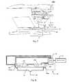
- FIG. 1depicts a lithographic system 10 in accordance with one embodiment of the present invention that includes a pair of spaced-apart bridge supports 12 having a bridge 14 and a stage support 16 extending therebetween. Bridge 14 and stage support 16 are spaced-apart. Coupled to bridge 14 is an imprint head 18 , which extends from bridge 14 toward stage support 16 and provides movement along the Z-axis. Disposed upon stage support 16 to face imprint head 18 is a motion stage 20 . Motion stage 20 is configured to move with respect to stage support 16 along X- and Y-axes.
- imprint head 18may provide movement along the X- and Y-axes, as well as in the Z-axis
- motion stage 20may provide movement in the Z-axis, as well as in the X and Y axes.
- An exemplary motion stage deviceis disclosed in U.S. patent application Ser. No. 10/194,414, filed Jul. 11, 2002, entitled “Step and Repeat Imprint Lithography Systems,” assigned to the assignee of the present invention, and which is incorporated by reference herein in its entirety.
- a radiation source 22is coupled to lithographic system 10 to impinge actinic radiation upon motion stage 20 .
- radiation source 22is coupled to bridge 14 and includes a power generator 23 connected to radiation source 22 .
- Operation of lithographic system 10is typically controlled by a processor 25 that is in data communication therewith.
- Mold 28includes a plurality of features defined by a plurality of spaced-apart recessions 28 a and protrusions 28 b .
- the plurality of featuresdefines an original pattern that is to be transferred into a substrate 30 positioned on motion stage 20 .
- imprint head 18 and/or motion stage 20may vary a distance “d” between mold 28 and substrate 30 .
- the features on mold 28may be imprinted into a flowable region of substrate 30 , discussed more fully below.
- Radiation source 22is located so that mold 28 is positioned between radiation source 22 and substrate 30 .
- mold 28is fabricated from a material that allows it to be substantially transparent to the radiation produced by radiation source 22 .
- a flowable regionsuch as an imprinting layer 34 , is disposed on a portion of a surface 32 that presents a substantially planar profile.
- a flowable regionmay be formed using any known technique, such as a hot embossing process disclosed in U.S. Pat. No. 5,772,905, which is incorporated by reference in its entirety herein, or a laser assisted direct imprinting (LADI) process of the type described by Chou et al. in Ultrafast and Direct Imprint of Nanostructures in Silicon , Nature, Col. 417, pp. 835-837, June 2002.
- LADIlaser assisted direct imprinting
- a flowable regionconsists of imprinting layer 34 being deposited as a plurality of spaced-apart discrete droplets 36 of a material 36 a on substrate 30 , discussed more fully below.
- An exemplary system for depositing droplets 36is disclosed in U.S. patent application Ser. No. 10/191,749, filed Jul. 9, 2002, entitled “System and Method for Dispensing Liquids,” assigned to the assignee of the present invention, and which is incorporated by reference herein in its entirety.
- Imprinting layer 34is formed from material 36 a that may be selectively polymerized and cross-linked to record the original pattern therein, defining a recorded pattern.
- An exemplary composition for material 36 ais disclosed in U.S. patent application Ser. No.
- Material 36 ais shown in FIG. 4 as being cross-linked at points 36 b , forming a cross-linked polymer material 36 c.
- the pattern recorded in imprinting layer 34is produced, in part, by mechanical contact with mold 28 .
- distance “d”is reduced to allow droplets 36 to come into mechanical contact with mold 28 , spreading droplets 36 so as to form imprinting layer 34 with a contiguous formation of material 36 a over surface 32 .
- distance “d”is reduced to allow sub-portions 34 a of imprinting layer 34 to ingress into and fill recessions 28 a.
- material 36 ais provided with the requisite properties to completely fill recessions 28 a , while covering surface 32 with a contiguous formation of material 36 a .
- sub-portions 34 b of imprinting layer 34 in superimposition with protrusions 28 bremain after the desired, usually minimum, distance “d” has been reached, leaving sub-portions 34 a with a thickness t 1 , and sub-portions 34 b with a thickness, t 2 .
- Thicknesses “t 1 ” and “t 2 ”may be any thickness desired, dependent upon the application.
- t 1is selected so as to be no greater than twice the width u of sub-portions 34 a , i.e., t 1 ⁇ 2u, shown more clearly in FIG. 5 .
- radiation source 22produces actinic radiation that polymerizes and cross-links material 36 a , forming cross-linked polymer material 36 c .
- the composition of imprinting layer 34transforms from material 36 a to cross-linked polymer material 36 c , which is a solid.
- cross-linked polymer material 36 cis solidified to provide side 34 c of imprinting layer 34 with a shape conforming to a shape of a surface 28 c of mold 28 , shown more clearly in FIG. 5 .
- imprint head 18shown in FIG. 2 , is moved to increase distance “d” so that mold 28 and imprinting layer 34 are spaced-apart.
- substrate 30 and imprinting layer 34may be etched to transfer the pattern of imprinting layer 34 into substrate 30 , providing a patterned surface 32 a , shown in FIG. 6 .
- the material from which imprinting layer 34 is formedmay be varied to define a relative etch rate with respect to substrate 30 , as desired.
- the relative etch rate of imprinting layer 34 to substrate 30may be in a range of about 1.5:1 to about 100:1.
- imprinting layer 34may be provided with an etch differential with respect to photo-resist material (not shown) selectively disposed thereon.
- the photo-resist material (not shown)may be provided to further pattern imprinting layer 34 , using known techniques. Any etch process may be employed, dependent upon the etch rate desired and the underlying constituents that form substrate 30 and imprinting layer 34 . Exemplary etch processes may include plasma etching, reactive ion etching, chemical wet etching and the like.
- template 26upon which mold 28 is present, is coupled to an imprint head housing 18 a via a chucking system 40 that includes a chuck body 42 .
- Chuck body 42is adapted to retain template 26 upon which mold 28 is attached employing vacuum techniques.
- chuck body 42includes one or more recesses 42 a that are in fluid communication with a pressure control system, such as a fluid supply system 70 .
- Fluid supply system 70may include one or more pumps to provide both positive and negative pressure, as well as a supply of fluid to facilitate reducing, if not preventing, trapping of gases, such as air, in imprinting layer 34 , shown in FIG. 5 .
- An exemplary chucking systemis disclosed in U.S. patent application Ser. No. 10/293,224, entitled “Chucking System For Modulating Shapes of Substrates,” assigned to the assignee of the present invention, and which is incorporated by reference in its entirety herein.
- template 26is brought into proximity with substrate 30 before patterning imprinting material 36 a , shown in FIG. 3 , is disposed on a region 77 of substrate 30 .
- template 26is brought within microns of substrate 30 , e.g., 15 microns more or less. It has been found desirable to perform localized control of the atmosphere 78 that is proximate to both template 26 and region 77 . For example, to avoid the deleterious effects of gases present in imprinting material 36 a , shown in FIG. 3 , and/or subsequently trapped in the patterned imprinting layer 34 , shown in FIG. 2 , it has been found beneficial to control the consistency of fluid in atmosphere 78 and/or the pressure of atmosphere 78 .
- chuck body 42is designed to facilitate the passage of fluids proximate to mold 28 and imprint head 18 includes a baffle 100 surrounding template 26 .
- baffle 100extends from imprint head 18 , terminating in a nadir 102 that lies in a plane in which a surface 26 a lies. In this fashion, mold 28 extends beyond nadir 102 to facilitate contact with region 77 .
- Chuck body 42includes one or more throughways, two of which are shown as 104 and 106 .
- Apertures 104 a and 106 a of throughways 104 and 106are disposed in a surface of chuck body 42 disposed between template 26 and baffle 100 , referred to as a peripheral surface 100 a .
- Throughways 104 and 106place apertures 104 a and 106 a in fluid communication with fluid supply system 70 , shown in FIG. 8 .
- Baffle 100functions to slow the movement of fluid exiting apertures 104 a and 106 a away from mold 28 .
- baffle 100includes first and second opposed surfaces 102 a and 102 b .
- First opposed surface 102 aextends from nadir 102 away from substrate 30 and faces template 26 .
- Second opposed surface 102 bextends from nadir 102 away from substrate 30 and faces away from mold 28 .
- first opposed surface 102 ais shown extending obliquely with respect to second opposing surface 102 b .
- atmosphere 78may be controlled by introduction or evacuation of fluid through apertures 104 a and 106 a .
- first and second opposed surfaces 102 a and 102 bmay extend parallel to one another from nadir 102 .
- atmosphere 78is established so that the transport of the gases present therein to either imprinting material 36 a in region 77 , substrate 31 , template 26 , mold 28 , or a combination thereof is increased.
- transportis defined to mean any mechanism by which the propagation of gases through either imprinting material 36 a , substrate 31 , template 26 , mold 28 , or a combination thereof is increased, e.g., increased solubility, increased diffusion and the like.
- fluid supply system 70may include a supply of imprinting material 36 a .
- imprinting material 36 amay be introduced through apertures 104 a and 106 a to saturate atmosphere 78 with imprinting material 36 a . This was found to reduce, if not completely do away with, the quantity of gases, such as air, trapped in the imprinting layer 34 , shown in FIG. 5 , during imprint processes. This is beneficial as it was found that the presence of air in imprinting layer 34 , shown in FIG. 5 , creates undesirable voids. Alternatively, it was found that by saturating atmosphere 78 with carbon dioxide and/or helium the quantity of air trapped in imprinting layer 34 , shown in FIG. 5 , was substantially reduced if not avoided. It should be understood that a mixture of imprinting material 36 a , carbon dioxide and/or helium may be introduced into atmosphere 78 to reduce the quantity of air trapped in imprinting layer 34 , shown in FIG. 5 .
- a difficulty encountered with respect to introducing fluidswas to ensure that the molecules in the fluid streams 104 b and 106 b exiting apertures 104 a and 106 a , respectively, traveled to a region of the atmosphere positioned between mold 28 and droplets 36 , and before contact of droplets 36 with mold 28 .
- This region of atmosphere 78is referred to as a processing region 78 a .
- apertures 104 a and 106 aare disposed about peripheral surface 100 a , which is spaced-apart from processing region 78 a .
- a memory(not shown) is in data communication with processor 25 .
- the memory(not shown) comprises a computer-readable medium having a computer-readable program embodied therein.
- the computer-readable programincludes instructions to pulse fluid streams 104 b and 106 b into atmosphere 78 having a desired mixture of molecules, discussed above. In this manner, laminar flow of fluid streams 104 b and 106 b may be avoided.
- fluid streams 104 b and 106 b with turbulent flowthe probability will be increased that a sufficient quantity of the molecules contained therein will reach processing region 78 a to reduce, if not avoid, the presence of gases being trapped in imprinting layer 34 .
- fluidmay be pulsed through both apertures 104 a and 106 a , concurrently, or sequentially pulsed through the same, i.e., first fluid is introduced through aperture 104 a and subsequently through aperture 106 a and then again through 104 a , with the process being repeated for a desired time or during the entire imprinting process.
- the timing of the flow of gas into processing region 78 ais important because it is desired that a sufficient quantity of molecules contained therein reach processing region 78 a before contact is made between mold 28 and droplets 36 .
- fluidmay be pulsed through one of the apertures, e.g., aperture 104 a , and then evacuated through the remaining aperture, e.g., aperture 106 a .
- fluidwould be drawn across processing region 78 a .
- Itmay also be advantageous to pulse the fluid through both apertures 104 a and 106 a , concurrently, then evacuate through both apertures 104 a and 106 a concurrently. It is desired, however, that the flow rate of fluid be established to minimize, if not avoid, movement of droplets 36 , shown in FIG. 2 .
- a first stepwould include introducing fluid into atmosphere 78 through both apertures 104 a and 106 a .
- a second stepwould include evacuating the fluid through one of apertures 104 a and 106 a , e.g., aperture 104 a .
- fluidwould be introduced into atmosphere 78 through both apertures 104 a and 106 a , concurrently.
- fluidwould be evacuated through one of apertures 104 a and 106 a that was not employed in the previous step to remove fluid, e.g., aperture 106 a .
- evacuationmay occur through one of apertures 104 a and 106 a , while fluid is being introduced through the remaining aperture of apertures 104 a and 106 a .
- evacuationmay occur in the absence of a fluid flow into atmosphere 78 .
- the desired resultis that fluid ingression into atmosphere 78 and fluid evacuation therefrom occurs so that the desired concentration of fluid is present.
- a plurality of aperturesmay be disposed about peripheral surface 100 a so that each of the apertures of a pair is disposed opposite one another on opposite sides of template 26 . This is shown by aperture pair 104 a and 106 a being disposed opposite one another on opposite sides of template 26 .
- a second aperture pairis shown as 108 a and 110 a .
- Apertures 108 a and 110 aare disposed opposite one another on opposite sides of template 26 .
- each of apertures 104 a , 106 a , 108 a and 110 aare arranged to lie on a common circle with adjacent apertures being spaced-apart therefrom by 90°.
- each of apertures 104 a , 106 a , 108 a and 110 aare arranged to facilitate fluid flow in/out of a different quadrant of chuck body 42 .
- aperture 104 afacilitates fluid flow in/out of quadrant I
- aperture 106 afacilitates fluid flow in/out of quadrant II
- aperture 108 afacilitates fluid flow in/out of quadrant III
- aperture 110 afacilitates fluid flow in/out of quadrant IV.
- any number of aperturesmay be employed, e.g., more than one per quadrant with differing quadrants having differing numbers of apertures and arranged in any spatial arrangement desired.
- Each of these arrangementsshould facilitate introduction and/or evacuation of a plurality of flows of fluid streams into atmosphere 78 , with a subset of the plurality of flows being introduced to differing regions about template 26 . It is believed that introduction of the multiple flows of fluid streams provides a turbulent flow of fluid in atmosphere 78 . This, it is believed, increases the probability that molecules in the fluid streams would reach processing region 78 a . However, fluid flow into atmosphere 78 through each of the apertures 104 a , 106 a , 108 a and 110 a and evacuation of fluid from atmosphere 78 therethrough may occur in any manner discussed above.
- a fluid streammay be introduced through each of apertures 104 a , 106 a , 108 a and 110 a sequentially so that a flow cell 112 may be created between template 26 and region 77 .
- Flow cell 112would facilitate ingression of molecules in the fluid streams into processing region 78 a to provide the benefits mentioned above. For example, first a fluid flow may be introduced through aperture 104 a and then terminated. After termination of fluid flow through aperture 104 a , fluid flow through aperture 106 a is commenced to introduce fluid into atmosphere 78 . Subsequently, fluid flow through aperture 106 a is terminated.
- fluid flow through aperture 108 ais commenced to introduce fluid into atmosphere 78 .
- Fluid flow in through aperture 108 ais subsequently terminated.
- fluid flow through aperture 110 ais commenced to introduce fluid into atmosphere 78 .
- fluidis introduced into atmosphere 78 through a single quadrant at any given time.
- sequential introduction and evacuation through apertures 104 a , 106 a , 108 a and 110 amay be undertaken to create flow cell 112 .
- sequential evacuationmay occur through each of apertures 104 a , 106 a , 108 a and 110 a to create flow cell 112 .
- fluidmay be introduced through all apertures in chuck body 42 , concurrently. Thereafter, fluid may be evacuated from each of apertures 104 a , 106 a , 108 a and 110 a , one at a time.
- the concentration in atmosphere 78 of fluid introduced through apertures 104 a , 106 a , 108 a and 110 awent below a desired level due to evacuation.
- the fluidmay then be reintroduced through one or all of apertures 104 a , 106 a , 108 a and 110 a again and the process repeated to create and/or maintain flow cell 112 .
Landscapes
- Engineering & Computer Science (AREA)
- Chemical & Material Sciences (AREA)
- Nanotechnology (AREA)
- Physics & Mathematics (AREA)
- General Physics & Mathematics (AREA)
- Crystallography & Structural Chemistry (AREA)
- Manufacturing & Machinery (AREA)
- Condensed Matter Physics & Semiconductors (AREA)
- Mathematical Physics (AREA)
- Theoretical Computer Science (AREA)
- Chemical Kinetics & Catalysis (AREA)
- Computer Hardware Design (AREA)
- Microelectronics & Electronic Packaging (AREA)
- Power Engineering (AREA)
- Shaping Of Tube Ends By Bending Or Straightening (AREA)
- Exposure Of Semiconductors, Excluding Electron Or Ion Beam Exposure (AREA)
Abstract
Description
- The present application is a continuation-in-part of U.S. patent application Ser. No. 10/898,034 filed on Jul. 23, 2004 entitled “Method for Creating a Turbulent Flow of Fluid Between a Mold and a Substrate” which is a divisional of U.S. Pat. No. 7,090,716 filed on Oct. 2, 2003 entitled “Single Phase Fluid Imprint Lithography Method,” all of which are incorporated by reference herein.
- The field of invention relates generally to imprint lithography. More particularly, the present invention is directed to a system for controlling a flow of a substance over an imprinting material.
- Micro-fabrication involves the fabrication of very small structures, e.g., having features on the order of micro-meters or smaller. One area in which micro-fabrication has had a sizeable impact is in the processing of integrated circuits. As the semiconductor processing industry continues to strive for larger production yields while increasing the circuits per unit area formed on a substrate, micro-fabrication becomes increasingly important. Micro-fabrication provides greater process control while allowing increased reduction of the minimum feature dimension of the structures formed. Other areas of development in which micro-fabrication has been employed include biotechnology, optical technology, mechanical systems and the like.
- An exemplary micro-fabrication technique is shown in U.S. Pat. No. 6,334,960 to Willson et al. Willson et al. disclose a method of forming a relief image in a structure. The method includes providing a substrate having a transfer layer. The transfer layer is covered with a polymerizable fluid composition. A mold makes mechanical contact with the polymerizable fluid. The mold includes a relief structure, and the polymerizable fluid composition fills the relief structure. The polymerizable fluid composition is then subjected to conditions to solidify and polymerize the same, forming a solidified polymeric material on the transfer layer that contains a relief structure complimentary to that of the mold. The mold is then separated from the solid polymeric material such that a replica of the relief structure in the mold is formed in the solidified polymeric material. The transfer layer and the solidified polymeric material are subjected to an environment to selectively etch the transfer layer relative to the solidified polymeric material such that a relief image is formed in the transfer layer. The time required and the minimum feature dimension provided by this technique is dependent upon, inter alia, the composition of the polymerizable material.
- U.S. Pat. No. 5,772,905 to Chou discloses a lithographic method and apparatus for creating ultra-fine (sub-25 nm) patterns in a thin film coated on a substrate in which a mold having at least one protruding feature is pressed into a thin film carried on a substrate. The protruding feature in the mold creates a recess of the thin film. The mold is removed from the film. The thin film then is processed such that the thin film in the recess is removed, exposing the underlying substrate. Thus, patterns in the mold are replaced in the thin film, completing the lithography. The patterns in the thin film will be, in subsequent processes, reproduced in the substrate or in another material which is added onto the substrate.
- Yet another imprint lithography technique is disclosed by Chou et al. inUltrafast and Direct Imprint of Nanostructures in Silicon, Nature, Col. 417, pp. 835-837, June 2002, which is referred to as a laser assisted direct imprinting (LADI) process. In this process. a region of a substrate is made flowable, e.g., liquefied, by heating the region with the laser. After the region has reached a desired viscosity, a mold, having a pattern thereon, is placed in contact with the region. The flowable region conforms to the profile of the pattern and is then cooled, solidifying the pattern into the substrate. A concern with this technique involves pattern distortions attributable to the presence of gases in the flowable region.
- It is desired, therefore, to provide a system to reduce distortions in patterns formed using imprint lithographic techniques.
FIG. 1 is a perspective view of a lithographic system in accordance with the present invention;FIG. 2 is a simplified elevation view of a lithographic system shown inFIG. 1 ;FIG. 3 is a simplified representation of material from which an imprinting layer, shown inFIG. 2 , is comprised before being polymerized and cross-linked;FIG. 4 is a simplified representation of cross-linked polymer material into which the material shown inFIG. 3 is transformed after being subjected to radiation;FIG. 5 is a simplified elevation view of a mold spaced-apart from the imprinting layer, shown inFIG. 1 , after patterning of the imprinting layer;FIG. 6 is a simplified elevation view of an additional imprinting layer positioned atop the substrate shown inFIG. 5 after the pattern in the first imprinting layer is transferred therein;FIG. 7 is a detailed perspective view of a print head shown inFIG. 1 ;FIG. 8 is a cross-sectional view of a chucking system in accordance with the present invention;FIG. 9 is detailed cross-sectional view of an imprint head shown inFIG. 7 ; andFIG. 10 is a bottom-up perspective view of the imprint head shown inFIG. 9 .FIG. 1 depicts a lithographic system10 in accordance with one embodiment of the present invention that includes a pair of spaced-apart bridge supports12 having a bridge14 and astage support 16 extending therebetween. Bridge14 andstage support 16 are spaced-apart. Coupled to bridge14 is animprint head 18, which extends from bridge14 towardstage support 16 and provides movement along the Z-axis. Disposed uponstage support 16 to faceimprint head 18 is amotion stage 20.Motion stage 20 is configured to move with respect tostage support 16 along X- and Y-axes. It should be understood thatimprint head 18 may provide movement along the X- and Y-axes, as well as in the Z-axis, andmotion stage 20 may provide movement in the Z-axis, as well as in the X and Y axes. An exemplary motion stage device is disclosed in U.S. patent application Ser. No. 10/194,414, filed Jul. 11, 2002, entitled “Step and Repeat Imprint Lithography Systems,” assigned to the assignee of the present invention, and which is incorporated by reference herein in its entirety. Aradiation source 22 is coupled to lithographic system10 to impinge actinic radiation uponmotion stage 20. As shown,radiation source 22 is coupled to bridge14 and includes apower generator 23 connected toradiation source 22. Operation of lithographic system10 is typically controlled by aprocessor 25 that is in data communication therewith.- Referring to both
FIGS. 1 and 2 , connected toimprint head 18 is atemplate 26 having amold 28 thereon.Mold 28 includes a plurality of features defined by a plurality of spaced-apart recessions 28aandprotrusions 28b. The plurality of features defines an original pattern that is to be transferred into a substrate30 positioned onmotion stage 20. To that end,imprint head 18 and/ormotion stage 20 may vary a distance “d” betweenmold 28 and substrate30. In this manner, the features onmold 28 may be imprinted into a flowable region of substrate30, discussed more fully below.Radiation source 22 is located so thatmold 28 is positioned betweenradiation source 22 and substrate30. As a result,mold 28 is fabricated from a material that allows it to be substantially transparent to the radiation produced byradiation source 22. - Referring to both
FIGS. 2 and 3 , a flowable region, such as animprinting layer 34, is disposed on a portion of asurface 32 that presents a substantially planar profile. A flowable region may be formed using any known technique, such as a hot embossing process disclosed in U.S. Pat. No. 5,772,905, which is incorporated by reference in its entirety herein, or a laser assisted direct imprinting (LADI) process of the type described by Chou et al. inUltrafast and Direct Imprint of Nanostructures in Silicon, Nature, Col. 417, pp. 835-837, June 2002. In the present embodiment, however, a flowable region consists ofimprinting layer 34 being deposited as a plurality of spaced-apartdiscrete droplets 36 of a material36aon substrate30, discussed more fully below. An exemplary system for depositingdroplets 36 is disclosed in U.S. patent application Ser. No. 10/191,749, filed Jul. 9, 2002, entitled “System and Method for Dispensing Liquids,” assigned to the assignee of the present invention, and which is incorporated by reference herein in its entirety. Imprintinglayer 34 is formed frommaterial 36athat may be selectively polymerized and cross-linked to record the original pattern therein, defining a recorded pattern. An exemplary composition formaterial 36ais disclosed in U.S. patent application Ser. No. 10/463,396, filed Jun. 16, 2003, and entitled “Method to Reduce Adhesion Between a Conformable Region and a Pattern of a Mold,” which is incorporated by reference in its entirety herein.Material 36ais shown inFIG. 4 as being cross-linked atpoints 36b, forming across-linked polymer material 36c. - Referring to
FIGS. 2 ,3 and5, the pattern recorded inimprinting layer 34 is produced, in part, by mechanical contact withmold 28. To that end, distance “d” is reduced to allowdroplets 36 to come into mechanical contact withmold 28, spreadingdroplets 36 so as to form imprintinglayer 34 with a contiguous formation ofmaterial 36aoversurface 32. In one embodiment, distance “d” is reduced to allow sub-portions34aofimprinting layer 34 to ingress into and fillrecessions 28a. - To facilitate filling of
recessions 28a,material 36ais provided with the requisite properties to completely fillrecessions 28a, while coveringsurface 32 with a contiguous formation ofmaterial 36a. In the present embodiment, sub-portions34bofimprinting layer 34 in superimposition withprotrusions 28bremain after the desired, usually minimum, distance “d” has been reached, leaving sub-portions34awith a thickness t1, and sub-portions34bwith a thickness, t2. Thicknesses “t1” and “t2” may be any thickness desired, dependent upon the application. Typically, t1is selected so as to be no greater than twice the width u of sub-portions34a, i.e., t1≦2u, shown more clearly inFIG. 5 . - Referring to
FIGS. 2 ,3 and4, after a desired distance “d” has been reached,radiation source 22 produces actinic radiation that polymerizes andcross-links material 36a, formingcross-linked polymer material 36c. As a result, the composition ofimprinting layer 34 transforms frommaterial 36atocross-linked polymer material 36c, which is a solid. Specifically,cross-linked polymer material 36cis solidified to provideside 34cofimprinting layer 34 with a shape conforming to a shape of asurface 28cofmold 28, shown more clearly inFIG. 5 . After imprintinglayer 34 is transformed to consist ofcross-linked polymer material 36c, shown inFIG. 4 ,imprint head 18, shown inFIG. 2 , is moved to increase distance “d” so thatmold 28 andimprinting layer 34 are spaced-apart. - Referring to
FIG. 5 , additional processing may be employed to complete the patterning of substrate30. For example, substrate30 andimprinting layer 34 may be etched to transfer the pattern ofimprinting layer 34 into substrate30, providing a patternedsurface 32a, shown inFIG. 6 . To facilitate etching, the material from whichimprinting layer 34 is formed may be varied to define a relative etch rate with respect to substrate30, as desired. The relative etch rate ofimprinting layer 34 to substrate30 may be in a range of about 1.5:1 to about 100:1. - Alternatively, or in addition to,
imprinting layer 34 may be provided with an etch differential with respect to photo-resist material (not shown) selectively disposed thereon. The photo-resist material (not shown) may be provided to furtherpattern imprinting layer 34, using known techniques. Any etch process may be employed, dependent upon the etch rate desired and the underlying constituents that form substrate30 andimprinting layer 34. Exemplary etch processes may include plasma etching, reactive ion etching, chemical wet etching and the like. - Referring to
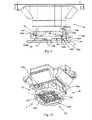
FIGS. 7 and 8 ,template 26, upon whichmold 28 is present, is coupled to animprint head housing 18avia achucking system 40 that includes achuck body 42. Chuckbody 42 is adapted to retaintemplate 26 upon whichmold 28 is attached employing vacuum techniques. To that end, chuckbody 42 includes one ormore recesses 42athat are in fluid communication with a pressure control system, such as afluid supply system 70.Fluid supply system 70 may include one or more pumps to provide both positive and negative pressure, as well as a supply of fluid to facilitate reducing, if not preventing, trapping of gases, such as air, inimprinting layer 34, shown inFIG. 5 . An exemplary chucking system is disclosed in U.S. patent application Ser. No. 10/293,224, entitled “Chucking System For Modulating Shapes of Substrates,” assigned to the assignee of the present invention, and which is incorporated by reference in its entirety herein. - As discussed above, during imprinting
template 26 and, therefore,mold 28, is brought into proximity with substrate30 before patterningimprinting material 36a, shown inFIG. 3 , is disposed on aregion 77 of substrate30. Specifically,template 26 is brought within microns of substrate30, e.g., 15 microns more or less. It has been found desirable to perform localized control of theatmosphere 78 that is proximate to bothtemplate 26 andregion 77. For example, to avoid the deleterious effects of gases present in imprintingmaterial 36a, shown inFIG. 3 , and/or subsequently trapped in the patternedimprinting layer 34, shown inFIG. 2 , it has been found beneficial to control the consistency of fluid inatmosphere 78 and/or the pressure ofatmosphere 78. - Referring to
FIG. 9 , to facilitate control ofatmosphere 78,chuck body 42 is designed to facilitate the passage of fluids proximate to mold28 andimprint head 18 includes abaffle 100 surroundingtemplate 26. Specifically, baffle100 extends fromimprint head 18, terminating in anadir 102 that lies in a plane in which asurface 26alies. In this fashion,mold 28 extends beyondnadir 102 to facilitate contact withregion 77. Chuckbody 42 includes one or more throughways, two of which are shown as104 and106.Apertures throughways chuck body 42 disposed betweentemplate 26 andbaffle 100, referred to as aperipheral surface 100a.Throughways place apertures fluid supply system 70, shown inFIG. 8 .Baffle 100 functions to slow the movement offluid exiting apertures mold 28. To that end,baffle 100 includes first and secondopposed surfaces opposed surface 102aextends fromnadir 102 away from substrate30 and facestemplate 26. Secondopposed surface 102bextends fromnadir 102 away from substrate30 and faces away frommold 28. Although it is not necessary, first opposedsurface 102ais shown extending obliquely with respect to second opposingsurface 102b. With this configuration,atmosphere 78 may be controlled by introduction or evacuation of fluid throughapertures opposed surfaces nadir 102. - Referring to
FIGS. 3 ,8 and9, in one embodiment,atmosphere 78 is established so that the transport of the gases present therein to eitherimprinting material 36ainregion 77,substrate 31,template 26,mold 28, or a combination thereof is increased. The term transport is defined to mean any mechanism by which the propagation of gases through eitherimprinting material 36a,substrate 31,template 26,mold 28, or a combination thereof is increased, e.g., increased solubility, increased diffusion and the like. To that end,fluid supply system 70 may include a supply ofimprinting material 36a. Under control ofprocessor 25, which is in data communication withfluid supply system 70, imprintingmaterial 36amay be introduced throughapertures atmosphere 78 withimprinting material 36a. This was found to reduce, if not completely do away with, the quantity of gases, such as air, trapped in theimprinting layer 34, shown inFIG. 5 , during imprint processes. This is beneficial as it was found that the presence of air inimprinting layer 34, shown inFIG. 5 , creates undesirable voids. Alternatively, it was found that by saturatingatmosphere 78 with carbon dioxide and/or helium the quantity of air trapped inimprinting layer 34, shown inFIG. 5 , was substantially reduced if not avoided. It should be understood that a mixture of imprintingmaterial 36a, carbon dioxide and/or helium may be introduced intoatmosphere 78 to reduce the quantity of air trapped inimprinting layer 34, shown inFIG. 5 . - Referring to
FIGS. 2 ,9 and10, a difficulty encountered with respect to introducing fluids was to ensure that the molecules in the fluid streams104band106bexitingapertures mold 28 anddroplets 36, and before contact ofdroplets 36 withmold 28. This region ofatmosphere 78 is referred to as aprocessing region 78a. As shown,apertures peripheral surface 100a, which is spaced-apart from processingregion 78a. Given that the separation ofmold 28 fromregion 77 is on the order of microns, the relative dimensions of the molecules influid streams mold 28 andregion 77 makes difficult the ingression of the aforementioned molecules intoprocessing region 78a. - Referring to
FIGS. 8 and 9 , one manner in which to overcome the aforementioned difficulty is to havefluid supply system 70 under control ofprocessor 25. A memory (not shown) is in data communication withprocessor 25. The memory (not shown) comprises a computer-readable medium having a computer-readable program embodied therein. The computer-readable program includes instructions to pulse fluid streams104band106bintoatmosphere 78 having a desired mixture of molecules, discussed above. In this manner, laminar flow offluid streams fluid streams processing region 78ato reduce, if not avoid, the presence of gases being trapped inimprinting layer 34. To that end, fluid may be pulsed through bothapertures aperture 104aand subsequently throughaperture 106aand then again through104a, with the process being repeated for a desired time or during the entire imprinting process. Furthermore, the timing of the flow of gas intoprocessing region 78ais important because it is desired that a sufficient quantity of molecules contained therein reachprocessing region 78abefore contact is made betweenmold 28 anddroplets 36. - Referring to
FIG. 9 , alternatively, fluid may be pulsed through one of the apertures, e.g.,aperture 104a, and then evacuated through the remaining aperture, e.g.,aperture 106a. In this manner, fluid would be drawn across processingregion 78a. It may also be advantageous to pulse the fluid through bothapertures apertures droplets 36, shown inFIG. 2 . - To ensure that the
fluids exiting apertures processing region 78a, it may be advantageous to concurrently pulse fluid through bothapertures apertures apertures atmosphere 78. Alternatingly evacuating the fluid through one ofapertures processing region 78a. For example, a first step would include introducing fluid intoatmosphere 78 through bothapertures apertures aperture 104a. Thereafter, at a third step, fluid would be introduced intoatmosphere 78 through bothapertures apertures aperture 106a. It should be understood that evacuation may occur through one ofapertures apertures atmosphere 78. The desired result is that fluid ingression intoatmosphere 78 and fluid evacuation therefrom occurs so that the desired concentration of fluid is present. - Referring to
FIGS. 9 and 10 , in another embodiment, a plurality of apertures may be disposed aboutperipheral surface 100aso that each of the apertures of a pair is disposed opposite one another on opposite sides oftemplate 26. This is shown byaperture pair template 26. A second aperture pair is shown as108aand110a.Apertures template 26. - As shown, each of
apertures apertures chuck body 42. Specifically,aperture 104afacilitates fluid flow in/out of quadrant I;aperture 106afacilitates fluid flow in/out of quadrant II;aperture 108afacilitates fluid flow in/out of quadrant III; andaperture 110afacilitates fluid flow in/out of quadrant IV. However, any number of apertures may be employed, e.g., more than one per quadrant with differing quadrants having differing numbers of apertures and arranged in any spatial arrangement desired. Each of these arrangements should facilitate introduction and/or evacuation of a plurality of flows of fluid streams intoatmosphere 78, with a subset of the plurality of flows being introduced to differing regions abouttemplate 26. It is believed that introduction of the multiple flows of fluid streams provides a turbulent flow of fluid inatmosphere 78. This, it is believed, increases the probability that molecules in the fluid streams would reachprocessing region 78a. However, fluid flow intoatmosphere 78 through each of theapertures atmosphere 78 therethrough may occur in any manner discussed above. - In another embodiment, a fluid stream may be introduced through each of
apertures flow cell 112 may be created betweentemplate 26 andregion 77.Flow cell 112 would facilitate ingression of molecules in the fluid streams intoprocessing region 78ato provide the benefits mentioned above. For example, first a fluid flow may be introduced throughaperture 104aand then terminated. After termination of fluid flow throughaperture 104a, fluid flow throughaperture 106ais commenced to introduce fluid intoatmosphere 78. Subsequently, fluid flow throughaperture 106ais terminated. After termination of fluid flow throughaperture 106a, fluid flow throughaperture 108ais commenced to introduce fluid intoatmosphere 78. Fluid flow in throughaperture 108ais subsequently terminated. After termination of fluid flow throughaperture 108a, fluid flow throughaperture 110ais commenced to introduce fluid intoatmosphere 78. In this manner, fluid is introduced intoatmosphere 78 through a single quadrant at any given time. However, it may be desirable to introduce fluid into more than one quadrant. Although this may frustrate creation offlow cell 112, it is within confines of the present invention. - Alternatively, sequential introduction and evacuation through
apertures flow cell 112. This would include introducing fluid through one or more ofapertures apertures flow cell 112. For example, fluid may be introduced through all apertures inchuck body 42, concurrently. Thereafter, fluid may be evacuated from each ofapertures atmosphere 78 of fluid introduced throughapertures apertures flow cell 112. - The embodiments of the present invention described above are exemplary. Many changes and modifications may be made to the disclosure recited above, while remaining within the scope of the invention. Therefore, the scope of the invention should not be limited by the above description, but instead should be determined with reference to the appended claims along with their full scope of equivalents.
Claims (24)
Priority Applications (6)
| Application Number | Priority Date | Filing Date | Title |
|---|---|---|---|
| US12/026,022US8211214B2 (en) | 2003-10-02 | 2008-02-05 | Single phase fluid imprint lithography method |
| PCT/US2009/000743WO2009099630A1 (en) | 2008-02-05 | 2009-02-05 | Single phase fluid imprint lithography method |
| JP2010545036AJP2011514658A (en) | 2008-02-05 | 2009-02-05 | Single phase fluid imprint lithography |
| KR1020107018536AKR20100112179A (en) | 2008-02-05 | 2009-02-05 | Single phase fluid imprint lithography method |
| CN2009801044625ACN101932754A (en) | 2008-02-05 | 2009-02-05 | Single-phase fluid imprint lithography method |
| EP09707651AEP2252725A4 (en) | 2008-02-05 | 2009-02-05 | SINGLE PHASE FLUID PRINTING LITHOGRAPHY METHOD |
Applications Claiming Priority (3)
| Application Number | Priority Date | Filing Date | Title |
|---|---|---|---|
| US10/677,639US7090716B2 (en) | 2003-10-02 | 2003-10-02 | Single phase fluid imprint lithography method |
| US10/898,034US7531025B2 (en) | 2003-10-02 | 2004-07-23 | Method of creating a turbulent flow of fluid between a mold and a substrate |
| US12/026,022US8211214B2 (en) | 2003-10-02 | 2008-02-05 | Single phase fluid imprint lithography method |
Related Parent Applications (1)
| Application Number | Title | Priority Date | Filing Date |
|---|---|---|---|
| US10/898,034Continuation-In-PartUS7531025B2 (en) | 2003-10-02 | 2004-07-23 | Method of creating a turbulent flow of fluid between a mold and a substrate |
Publications (2)
| Publication Number | Publication Date |
|---|---|
| US20080141862A1true US20080141862A1 (en) | 2008-06-19 |
| US8211214B2 US8211214B2 (en) | 2012-07-03 |
Family
ID=39525580
Family Applications (1)
| Application Number | Title | Priority Date | Filing Date |
|---|---|---|---|
| US12/026,022Active2026-07-01US8211214B2 (en) | 2003-10-02 | 2008-02-05 | Single phase fluid imprint lithography method |
Country Status (6)
| Country | Link |
|---|---|
| US (1) | US8211214B2 (en) |
| EP (1) | EP2252725A4 (en) |
| JP (1) | JP2011514658A (en) |
| KR (1) | KR20100112179A (en) |
| CN (1) | CN101932754A (en) |
| WO (1) | WO2009099630A1 (en) |
Cited By (21)
| Publication number | Priority date | Publication date | Assignee | Title |
|---|---|---|---|---|
| US20080174046A1 (en)* | 2002-07-11 | 2008-07-24 | Molecular Imprints Inc. | Capillary Imprinting Technique |
| US20080303187A1 (en)* | 2006-12-29 | 2008-12-11 | Molecular Imprints, Inc. | Imprint Fluid Control |
| US20090014917A1 (en)* | 2007-07-10 | 2009-01-15 | Molecular Imprints, Inc. | Drop Pattern Generation for Imprint Lithography |
| US20090115110A1 (en)* | 2007-11-02 | 2009-05-07 | Molecular Imprints, Inc. | Drop Pattern Generation for Imprint Lithography |
| US20090140445A1 (en)* | 2007-12-04 | 2009-06-04 | Molecular Imprints | High Throughput Imprint Based on Contact Line Motion Tracking Control |
| US20090200710A1 (en)* | 2008-02-08 | 2009-08-13 | Molecular Imprints, Inc. | Extrusion reduction in imprint lithography |
| US20090243153A1 (en)* | 2008-04-01 | 2009-10-01 | Molecular Imprints, Inc. | Large Area Roll-To-Roll Imprint Lithography |
| US7670530B2 (en) | 2006-01-20 | 2010-03-02 | Molecular Imprints, Inc. | Patterning substrates employing multiple chucks |
| US7670529B2 (en) | 2005-12-08 | 2010-03-02 | Molecular Imprints, Inc. | Method and system for double-sided patterning of substrates |
| US7691313B2 (en) | 2002-11-13 | 2010-04-06 | Molecular Imprints, Inc. | Method for expelling gas positioned between a substrate and a mold |
| US20100098859A1 (en)* | 2008-10-21 | 2010-04-22 | Molecular Imprints, Inc. | Drop Pattern Generation with Edge Weighting |
| US20110012297A1 (en)* | 2009-07-17 | 2011-01-20 | Kobiki Ayumi | Pattern transfer method |
| US7981481B2 (en) | 2004-09-23 | 2011-07-19 | Molecular Imprints, Inc. | Method for controlling distribution of fluid components on a body |
| US8012395B2 (en) | 2006-04-18 | 2011-09-06 | Molecular Imprints, Inc. | Template having alignment marks formed of contrast material |
| US20120080820A1 (en)* | 2010-10-04 | 2012-04-05 | Canon Kabushiki Kaisha | Imprinting method |
| US8215946B2 (en) | 2006-05-18 | 2012-07-10 | Molecular Imprints, Inc. | Imprint lithography system and method |
| US20120299222A1 (en)* | 2010-12-22 | 2012-11-29 | Qingdao Technological University | Method and device for full wafer nanoimprint lithography |
| US8586126B2 (en) | 2008-10-21 | 2013-11-19 | Molecular Imprints, Inc. | Robust optimization to generate drop patterns in imprint lithography which are tolerant of variations in drop volume and drop placement |
| JP2013254782A (en)* | 2012-06-05 | 2013-12-19 | Canon Inc | Imprint method and imprint device, and method for manufacturing article using the same |
| WO2013192018A3 (en)* | 2012-06-19 | 2014-05-15 | Seagate Technology Llc | Nano-scale void reduction |
| US20230373173A1 (en)* | 2016-08-26 | 2023-11-23 | Molecular Imprints, Inc. | Monolithic high refractive index photonic devices |
Families Citing this family (9)
| Publication number | Priority date | Publication date | Assignee | Title |
|---|---|---|---|---|
| WO2009129441A2 (en)* | 2008-04-17 | 2009-10-22 | Massachusetts Institute Of Technology | Symmetric thermocentric flexure with minimal yaw error motion |
| JP5491931B2 (en)* | 2010-03-30 | 2014-05-14 | 富士フイルム株式会社 | Nanoimprint method and mold manufacturing method |
| KR20130085759A (en) | 2012-01-20 | 2013-07-30 | 삼성전자주식회사 | Stamp and method of fabricating stamp and imprinting method using the same |
| JP5868215B2 (en) | 2012-02-27 | 2016-02-24 | キヤノン株式会社 | Imprint apparatus, imprint method, and article manufacturing method using the same |
| JP6643048B2 (en)* | 2015-11-09 | 2020-02-12 | キヤノン株式会社 | Apparatus for processing substrate, method for manufacturing article, and gas supply path |
| JP7041121B2 (en) | 2016-08-03 | 2022-03-23 | ボード オブ リージェンツ,ザ ユニバーシティ オブ テキサス システム | Wafer-scale programmable membrane for semiconductor flattening and imprint lithography |
| JP6978853B2 (en) | 2017-05-15 | 2021-12-08 | キヤノン株式会社 | Imprint device and article manufacturing method |
| US10895806B2 (en)* | 2017-09-29 | 2021-01-19 | Canon Kabushiki Kaisha | Imprinting method and apparatus |
| CN112657794A (en)* | 2020-05-13 | 2021-04-16 | 绍兴权电科技有限公司 | Multi-station anti-counterfeiting paste printing method based on inflation |
Citations (90)
| Publication number | Priority date | Publication date | Assignee | Title |
|---|---|---|---|---|
| US3783520A (en)* | 1970-09-28 | 1974-01-08 | Bell Telephone Labor Inc | High accuracy alignment procedure utilizing moire patterns |
| US4070116A (en)* | 1975-06-23 | 1978-01-24 | International Business Machines Corporation | Gap measuring device for defining the distance between two or more surfaces |
| US4201800A (en)* | 1978-04-28 | 1980-05-06 | International Business Machines Corp. | Hardened photoresist master image mask process |
| US4267212A (en)* | 1978-09-20 | 1981-05-12 | Fuji Photo Film Co., Ltd. | Spin coating process |
| US4426247A (en)* | 1982-04-12 | 1984-01-17 | Nippon Telegraph & Telephone Public Corporation | Method for forming micropattern |
| US4451507A (en)* | 1982-10-29 | 1984-05-29 | Rca Corporation | Automatic liquid dispensing apparatus for spinning surface of uniform thickness |
| US4507331A (en)* | 1983-12-12 | 1985-03-26 | International Business Machines Corporation | Dry process for forming positive tone micro patterns |
| US4512848A (en)* | 1984-02-06 | 1985-04-23 | Exxon Research And Engineering Co. | Procedure for fabrication of microstructures over large areas using physical replication |
| US4657845A (en)* | 1986-01-14 | 1987-04-14 | International Business Machines Corporation | Positive tone oxygen plasma developable photoresist |
| US4731155A (en)* | 1987-04-15 | 1988-03-15 | General Electric Company | Process for forming a lithographic mask |
| US4737425A (en)* | 1986-06-10 | 1988-04-12 | International Business Machines Corporation | Patterned resist and process |
| US4808511A (en)* | 1987-05-19 | 1989-02-28 | International Business Machines Corporation | Vapor phase photoresist silylation process |
| US4826943A (en)* | 1986-07-25 | 1989-05-02 | Oki Electric Industry Co., Ltd. | Negative resist material |
| US4891303A (en)* | 1988-05-26 | 1990-01-02 | Texas Instruments Incorporated | Trilayer microlithographic process using a silicon-based resist as the middle layer |
| US4908298A (en)* | 1985-03-19 | 1990-03-13 | International Business Machines Corporation | Method of creating patterned multilayer films for use in production of semiconductor circuits and systems |
| US4919748A (en)* | 1989-06-30 | 1990-04-24 | At&T Bell Laboratories | Method for tapered etching |
| US4921778A (en)* | 1988-07-29 | 1990-05-01 | Shipley Company Inc. | Photoresist pattern fabrication employing chemically amplified metalized material |
| US4931351A (en)* | 1987-01-12 | 1990-06-05 | Eastman Kodak Company | Bilayer lithographic process |
| US4999280A (en)* | 1989-03-17 | 1991-03-12 | International Business Machines Corporation | Spray silylation of photoresist images |
| US5179863A (en)* | 1990-03-05 | 1993-01-19 | Kabushiki Kaisha Toshiba | Method and apparatus for setting the gap distance between a mask and a wafer at a predetermined distance |
| US5198326A (en)* | 1990-05-24 | 1993-03-30 | Matsushita Electric Industrial Co., Ltd. | Process for forming fine pattern |
| US5212147A (en)* | 1991-05-15 | 1993-05-18 | Hewlett-Packard Company | Method of forming a patterned in-situ high Tc superconductive film |
| US5314772A (en)* | 1990-10-09 | 1994-05-24 | Arizona Board Of Regents | High resolution, multi-layer resist for microlithography and method therefor |
| US5318870A (en)* | 1989-10-18 | 1994-06-07 | Massachusetts Institute Of Technology | Method of patterning a phenolic polymer film without photoactive additive through exposure to high energy radiation below 225 nm with subsequent organometallic treatment and the associated imaged article |
| US5324683A (en)* | 1993-06-02 | 1994-06-28 | Motorola, Inc. | Method of forming a semiconductor structure having an air region |
| US5380474A (en)* | 1993-05-20 | 1995-01-10 | Sandia Corporation | Methods for patterned deposition on a substrate |
| US5417802A (en)* | 1994-03-18 | 1995-05-23 | At&T Corp. | Integrated circuit manufacturing |
| US5422295A (en)* | 1992-12-10 | 1995-06-06 | Samsung Electronics Co., Ltd. | Method for forming a semiconductor memory device having a vertical multi-layered storage electrode |
| US5421981A (en)* | 1991-06-26 | 1995-06-06 | Ppg Industries, Inc. | Electrochemical sensor storage device |
| US5480047A (en)* | 1993-06-04 | 1996-01-02 | Sharp Kabushiki Kaisha | Method for forming a fine resist pattern |
| US5512131A (en)* | 1993-10-04 | 1996-04-30 | President And Fellows Of Harvard College | Formation of microstamped patterns on surfaces and derivative articles |
| US5601641A (en)* | 1992-07-21 | 1997-02-11 | Tse Industries, Inc. | Mold release composition with polybutadiene and method of coating a mold core |
| US5723176A (en)* | 1994-03-02 | 1998-03-03 | Telecommunications Research Laboratories | Method and apparatus for making optical components by direct dispensing of curable liquid |
| US5736424A (en)* | 1987-02-27 | 1998-04-07 | Lucent Technologies Inc. | Device fabrication involving planarization |
| US5743998A (en)* | 1995-04-19 | 1998-04-28 | Park Scientific Instruments | Process for transferring microminiature patterns using spin-on glass resist media |
| US5753014A (en)* | 1993-11-12 | 1998-05-19 | Van Rijn; Cornelis Johannes Maria | Membrane filter and a method of manufacturing the same as well as a membrane |
| US5855686A (en)* | 1994-05-24 | 1999-01-05 | Depositech, Inc. | Method and apparatus for vacuum deposition of highly ionized media in an electromagnetic controlled environment |
| US5895263A (en)* | 1996-12-19 | 1999-04-20 | International Business Machines Corporation | Process for manufacture of integrated circuit device |
| US5900160A (en)* | 1993-10-04 | 1999-05-04 | President And Fellows Of Harvard College | Methods of etching articles via microcontact printing |
| US5907782A (en)* | 1998-08-15 | 1999-05-25 | Acer Semiconductor Manufacturing Inc. | Method of forming a multiple fin-pillar capacitor for a high density dram cell |
| US6033977A (en)* | 1997-06-30 | 2000-03-07 | Siemens Aktiengesellschaft | Dual damascene structure |
| US6039897A (en)* | 1996-08-28 | 2000-03-21 | University Of Washington | Multiple patterned structures on a single substrate fabricated by elastomeric micro-molding techniques |
| US6168845B1 (en)* | 1999-01-19 | 2001-01-02 | International Business Machines Corporation | Patterned magnetic media and method of making the same using selective oxidation |
| US6180239B1 (en)* | 1993-10-04 | 2001-01-30 | President And Fellows Of Harvard College | Microcontact printing on surfaces and derivative articles |
| US6218316B1 (en)* | 1998-10-22 | 2001-04-17 | Micron Technology, Inc. | Planarization of non-planar surfaces in device fabrication |
| US6334960B1 (en)* | 1999-03-11 | 2002-01-01 | Board Of Regents, The University Of Texas System | Step and flash imprint lithography |
| US20020018190A1 (en)* | 2000-06-15 | 2002-02-14 | Hideki Nogawa | Exposure apparatus and device manufacturing method |
| US6355198B1 (en)* | 1996-03-15 | 2002-03-12 | President And Fellows Of Harvard College | Method of forming articles including waveguides via capillary micromolding and microtransfer molding |
| US20020042027A1 (en)* | 1998-10-09 | 2002-04-11 | Chou Stephen Y. | Microscale patterning and articles formed thereby |
| US6383928B1 (en)* | 1999-09-02 | 2002-05-07 | Texas Instruments Incorporated | Post copper CMP clean |
| US6388253B1 (en)* | 1999-06-29 | 2002-05-14 | Applied Materials, Inc. | Integrated critical dimension control for semiconductor device manufacturing |
| US6387783B1 (en)* | 1999-04-26 | 2002-05-14 | International Business Machines Corporation | Methods of T-gate fabrication using a hybrid resist |
| US6391217B2 (en)* | 1999-12-23 | 2002-05-21 | University Of Massachusetts | Methods and apparatus for forming submicron patterns on films |
| US6391798B1 (en)* | 1987-02-27 | 2002-05-21 | Agere Systems Guardian Corp. | Process for planarization a semiconductor substrate |
| US6514672B2 (en)* | 1999-06-17 | 2003-02-04 | Taiwan Semiconductor Manufacturing Company | Dry development process for a bi-layer resist system |
| US6518189B1 (en)* | 1995-11-15 | 2003-02-11 | Regents Of The University Of Minnesota | Method and apparatus for high density nanostructures |
| US6517995B1 (en)* | 1999-09-14 | 2003-02-11 | Massachusetts Institute Of Technology | Fabrication of finely featured devices by liquid embossing |
| US20030034329A1 (en)* | 1998-06-30 | 2003-02-20 | Chou Stephen Y. | Lithographic method for molding pattern with nanoscale depth |
| US6534418B1 (en)* | 2001-04-30 | 2003-03-18 | Advanced Micro Devices, Inc. | Use of silicon containing imaging layer to define sub-resolution gate structures |
| US6541360B1 (en)* | 2001-04-30 | 2003-04-01 | Advanced Micro Devices, Inc. | Bi-layer trim etch process to form integrated circuit gate structures |
| US20030062334A1 (en)* | 2001-09-25 | 2003-04-03 | Lee Hong Hie | Method for forming a micro-pattern on a substrate by using capillary force |
| US20030081193A1 (en)* | 2001-06-01 | 2003-05-01 | White Donald L. | Holder, system, and process for improving overlay in lithography |
| US20030080472A1 (en)* | 2001-10-29 | 2003-05-01 | Chou Stephen Y. | Lithographic method with bonded release layer for molding small patterns |
| US6561706B2 (en)* | 2001-06-28 | 2003-05-13 | Advanced Micro Devices, Inc. | Critical dimension monitoring from latent image |
| US6565928B2 (en)* | 1999-03-08 | 2003-05-20 | Tokyo Electron Limited | Film forming method and film forming apparatus |
| US20040029041A1 (en)* | 2002-02-27 | 2004-02-12 | Brewer Science, Inc. | Novel planarization method for multi-layer lithography processing |
| US6696220B2 (en)* | 2000-10-12 | 2004-02-24 | Board Of Regents, The University Of Texas System | Template for room temperature, low pressure micro-and nano-imprint lithography |
| US20040036201A1 (en)* | 2000-07-18 | 2004-02-26 | Princeton University | Methods and apparatus of field-induced pressure imprint lithography |
| US6703190B2 (en)* | 1999-12-07 | 2004-03-09 | Infineon Technologies Ag | Method for producing resist structures |
| US20040046288A1 (en)* | 2000-07-18 | 2004-03-11 | Chou Stephen Y. | Laset assisted direct imprint lithography |
| US6716767B2 (en)* | 2001-10-31 | 2004-04-06 | Brewer Science, Inc. | Contact planarization materials that generate no volatile byproducts or residue during curing |
| US6730256B1 (en)* | 2000-08-04 | 2004-05-04 | Massachusetts Institute Of Technology | Stereolithographic patterning with interlayer surface modifications |
| US6737202B2 (en)* | 2002-02-22 | 2004-05-18 | Motorola, Inc. | Method of fabricating a tiered structure using a multi-layered resist stack and use |
| US6842229B2 (en)* | 2000-07-16 | 2005-01-11 | Board Of Regents, The University Of Texas System | Imprint lithography template comprising alignment marks |
| US6849558B2 (en)* | 2002-05-22 | 2005-02-01 | The Board Of Trustees Of The Leland Stanford Junior University | Replication and transfer of microstructures and nanostructures |
| US20050037143A1 (en)* | 2000-07-18 | 2005-02-17 | Chou Stephen Y. | Imprint lithography with improved monitoring and control and apparatus therefor |
| US20050061773A1 (en)* | 2003-08-21 | 2005-03-24 | Byung-Jin Choi | Capillary imprinting technique |
| US6871558B2 (en)* | 2002-12-12 | 2005-03-29 | Molecular Imprints, Inc. | Method for determining characteristics of substrate employing fluid geometries |
| US20050072757A1 (en)* | 2003-10-02 | 2005-04-07 | University Of Texas System Board Of Regents | Method of creating a turbulent flow of fluid between a mold and a substrate |
| US6890688B2 (en)* | 2001-12-18 | 2005-05-10 | Freescale Semiconductor, Inc. | Lithographic template and method of formation and use |
| US20050106321A1 (en)* | 2003-11-14 | 2005-05-19 | Molecular Imprints, Inc. | Dispense geometery to achieve high-speed filling and throughput |
| US6900881B2 (en)* | 2002-07-11 | 2005-05-31 | Molecular Imprints, Inc. | Step and repeat imprint lithography systems |
| US20060062922A1 (en)* | 2004-09-23 | 2006-03-23 | Molecular Imprints, Inc. | Polymerization technique to attenuate oxygen inhibition of solidification of liquids and composition therefor |
| US20060063112A1 (en)* | 2004-09-21 | 2006-03-23 | Molecular Imprints, Inc. | Pattern reversal employing thick residual layers |
| US7019819B2 (en)* | 2002-11-13 | 2006-03-28 | Molecular Imprints, Inc. | Chucking system for modulating shapes of substrates |
| US20060076717A1 (en)* | 2002-07-11 | 2006-04-13 | Molecular Imprints, Inc. | Step and repeat imprint lithography processes |
| US7157036B2 (en)* | 2003-06-17 | 2007-01-02 | Molecular Imprints, Inc | Method to reduce adhesion between a conformable region and a pattern of a mold |
| US20070063384A1 (en)* | 2005-09-21 | 2007-03-22 | Molecular Imprints, Inc. | Method to control an atmostphere between a body and a substrate |
| US7338275B2 (en)* | 2002-07-11 | 2008-03-04 | Molecular Imprints, Inc. | Formation of discontinuous films during an imprint lithography process |
| US7365103B2 (en)* | 2002-12-12 | 2008-04-29 | Board Of Regents, The University Of Texas System | Compositions for dark-field polymerization and method of using the same for imprint lithography processes |
Family Cites Families (111)
| Publication number | Priority date | Publication date | Assignee | Title |
|---|---|---|---|---|
| IT1068535B (en) | 1975-11-03 | 1985-03-21 | Ibm | APPARATUS AND GRAPHIC ELECTROLYTE PROCESS |
| DE2800476A1 (en) | 1977-01-07 | 1978-07-13 | Instruments Sa | Mass prodn. method for grids, graticules etc. - using revolving drum, belt carrying resin and UV light source for polymerisation process |
| US4279628A (en) | 1979-12-31 | 1981-07-21 | Energy Synergistics, Inc. | Apparatus for drying a natural gas stream |
| US4544572A (en) | 1982-09-07 | 1985-10-01 | Minnesota Mining And Manufacturing Company | Coated ophthalmic lenses and method for coating the same |
| FR2538923A1 (en) | 1982-12-30 | 1984-07-06 | Thomson Csf | METHOD AND DEVICE FOR OPTICALLY ALIGNING PATTERNS IN TWO PLANS RECONCILED IN AN EXPOSURE APPARATUS COMPRISING A DIVERGENT RADIATION SOURCE |
| US4552833A (en) | 1984-05-14 | 1985-11-12 | International Business Machines Corporation | Radiation sensitive and oxygen plasma developable resist |
| EP0228671A1 (en) | 1985-12-23 | 1987-07-15 | General Electric Company | Method for the production of a coated substrate with controlled surface characteristics |
| US4692205A (en) | 1986-01-31 | 1987-09-08 | International Business Machines Corporation | Silicon-containing polyimides as oxygen etch stop and dual dielectric coatings |
| KR900004269B1 (en) | 1986-06-11 | 1990-06-18 | 가부시기가이샤 도시바 | Method and device for positioing 1st body and 2nd body |
| JPS6376330A (en) | 1986-09-18 | 1988-04-06 | Oki Electric Ind Co Ltd | Manufacture of semiconductor device |
| US4707218A (en) | 1986-10-28 | 1987-11-17 | International Business Machines Corporation | Lithographic image size reduction |
| KR930000293B1 (en) | 1987-10-26 | 1993-01-15 | 마쯔시다덴기산교 가부시기가이샤 | Fine pattern formation method |
| US5028366A (en) | 1988-01-12 | 1991-07-02 | Air Products And Chemicals, Inc. | Water based mold release compositions for making molded polyurethane foam |
| US5821175A (en) | 1988-07-08 | 1998-10-13 | Cauldron Limited Partnership | Removal of surface contaminants by irradiation using various methods to achieve desired inert gas flow over treated surface |
| JPH0269936A (en) | 1988-07-28 | 1990-03-08 | Siemens Ag | Method for forming resin structures on semiconductor materials |
| EP0355496A3 (en) | 1988-08-15 | 1990-10-10 | Sumitomo Heavy Industries Co., Ltd. | Position detector employing a sector fresnel zone plate |
| JP2546350B2 (en) | 1988-09-09 | 1996-10-23 | キヤノン株式会社 | Alignment device |
| US4964945A (en) | 1988-12-09 | 1990-10-23 | Minnesota Mining And Manufacturing Company | Lift off patterning process on a flexible substrate |
| US5439766A (en) | 1988-12-30 | 1995-08-08 | International Business Machines Corporation | Composition for photo imaging |
| CA2010169A1 (en) | 1989-02-21 | 1990-08-21 | Masakazu Uekita | Multi-layer resist |
| US5169494A (en) | 1989-03-27 | 1992-12-08 | Matsushita Electric Industrial Co., Ltd. | Fine pattern forming method |
| DE59010728D1 (en) | 1989-04-24 | 1997-07-31 | Siemens Ag | Process for producing etch-resistant structures |
| JP3001607B2 (en) | 1989-04-24 | 2000-01-24 | シーメンス、アクチエンゲゼルシヤフト | Dimensionally stable structure transfer method in two-layer method |
| US5053318A (en) | 1989-05-18 | 1991-10-01 | Shipley Company Inc. | Plasma processing with metal mask integration |
| CA2011927C (en) | 1989-06-02 | 1996-12-24 | Alan Lee Sidman | Microlithographic method for producing thick, vertically-walled photoresist patterns |
| JP2704001B2 (en) | 1989-07-18 | 1998-01-26 | キヤノン株式会社 | Position detection device |
| DE4031637C2 (en) | 1989-10-06 | 1997-04-10 | Toshiba Kawasaki Kk | Arrangement for measuring a displacement between two objects |
| US5362606A (en) | 1989-10-18 | 1994-11-08 | Massachusetts Institute Of Technology | Positive resist pattern formation through focused ion beam exposure and surface barrier silylation |
| US5328810A (en) | 1990-05-07 | 1994-07-12 | Micron Technology, Inc. | Method for reducing, by a factor or 2-N, the minimum masking pitch of a photolithographic process |
| JP2524436B2 (en) | 1990-09-18 | 1996-08-14 | インターナショナル・ビジネス・マシーンズ・コーポレイション | Surface treatment method |
| US5240878A (en) | 1991-04-26 | 1993-08-31 | International Business Machines Corporation | Method for forming patterned films on a substrate |
| EP0524759A1 (en) | 1991-07-23 | 1993-01-27 | AT&T Corp. | Device fabrication process |
| US5242711A (en) | 1991-08-16 | 1993-09-07 | Rockwell International Corp. | Nucleation control of diamond films by microlithographic patterning |
| JPH0580530A (en) | 1991-09-24 | 1993-04-02 | Hitachi Ltd | Production of thin film pattern |
| US5263073A (en) | 1991-12-20 | 1993-11-16 | Board Of Supervisors Of Louisiana State University And Agricultural And Mechanical College | Scanning systems for high resolution E-beam and X-ray lithography |
| US5244818A (en) | 1992-04-08 | 1993-09-14 | Georgia Tech Research Corporation | Processes for lift-off of thin film materials and for the fabrication of three dimensional integrated circuits |
| US5545367A (en) | 1992-04-15 | 1996-08-13 | Soane Technologies, Inc. | Rapid prototype three dimensional stereolithography |
| US5376810A (en) | 1992-06-26 | 1994-12-27 | California Institute Of Technology | Growth of delta-doped layers on silicon CCD/S for enhanced ultraviolet response |
| US5431777A (en) | 1992-09-17 | 1995-07-11 | International Business Machines Corporation | Methods and compositions for the selective etching of silicon |
| DE69405451T2 (en) | 1993-03-16 | 1998-03-12 | Koninkl Philips Electronics Nv | Method and device for producing a structured relief image from cross-linked photoresist on a flat substrate surface |
| US5776748A (en) | 1993-10-04 | 1998-07-07 | President And Fellows Of Harvard College | Method of formation of microstamped patterns on plates for adhesion of cells and other biological materials, devices and uses therefor |
| US6776094B1 (en) | 1993-10-04 | 2004-08-17 | President & Fellows Of Harvard College | Kit For Microcontact Printing |
| KR970009858B1 (en) | 1994-01-12 | 1997-06-18 | 엘지반도체 주식회사 | Multi-layer photoresist patterning method |
| US5453157A (en) | 1994-05-16 | 1995-09-26 | Texas Instruments Incorporated | Low temperature anisotropic ashing of resist for semiconductor fabrication |
| US5458520A (en) | 1994-12-13 | 1995-10-17 | International Business Machines Corporation | Method for producing planar field emission structure |
| US5849209A (en) | 1995-03-31 | 1998-12-15 | Johnson & Johnson Vision Products, Inc. | Mold material made with additives |
| US5820769A (en) | 1995-05-24 | 1998-10-13 | Regents Of The University Of Minnesota | Method for making magnetic storage having discrete elements with quantized magnetic moments |
| US5948570A (en) | 1995-05-26 | 1999-09-07 | Lucent Technologies Inc. | Process for dry lithographic etching |
| US5997273A (en) | 1995-08-01 | 1999-12-07 | Laquer; Henry Louis | Differential pressure HIP forging in a controlled gaseous environment |
| US5654238A (en) | 1995-08-03 | 1997-08-05 | International Business Machines Corporation | Method for etching vertical contact holes without substrate damage caused by directional etching |
| US5849222A (en) | 1995-09-29 | 1998-12-15 | Johnson & Johnson Vision Products, Inc. | Method for reducing lens hole defects in production of contact lens blanks |
| US20040137734A1 (en) | 1995-11-15 | 2004-07-15 | Princeton University | Compositions and processes for nanoimprinting |
| US5772905A (en) | 1995-11-15 | 1998-06-30 | Regents Of The University Of Minnesota | Nanoimprint lithography |
| US7758794B2 (en) | 2001-10-29 | 2010-07-20 | Princeton University | Method of making an article comprising nanoscale patterns with reduced edge roughness |
| US6482742B1 (en) | 2000-07-18 | 2002-11-19 | Stephen Y. Chou | Fluid pressure imprint lithography |
| US5669303A (en) | 1996-03-04 | 1997-09-23 | Motorola | Apparatus and method for stamping a surface |
| US6143412A (en) | 1997-02-10 | 2000-11-07 | President And Fellows Of Harvard College | Fabrication of carbon microstructures |
| US5948470A (en) | 1997-04-28 | 1999-09-07 | Harrison; Christopher | Method of nanoscale patterning and products made thereby |
| US5948219A (en) | 1997-05-07 | 1999-09-07 | Advanced Micro Devices, Inc. | Apparatus for selectively exposing a semiconductor topography to an electric field |
| US5926690A (en) | 1997-05-28 | 1999-07-20 | Advanced Micro Devices, Inc. | Run-to-run control process for controlling critical dimensions |
| US5912049A (en) | 1997-08-12 | 1999-06-15 | Micron Technology, Inc. | Process liquid dispense method and apparatus |
| US5991022A (en) | 1997-12-09 | 1999-11-23 | N&K Technology, Inc. | Reflectance spectrophotometric apparatus with toroidal mirrors |
| US6150680A (en) | 1998-03-05 | 2000-11-21 | Welch Allyn, Inc. | Field effect semiconductor device having dipole barrier |
| JP3780700B2 (en) | 1998-05-26 | 2006-05-31 | セイコーエプソン株式会社 | Pattern forming method, pattern forming apparatus, pattern forming plate, pattern forming plate manufacturing method, color filter manufacturing method, conductive film manufacturing method, and liquid crystal panel manufacturing method |
| US6150231A (en) | 1998-06-15 | 2000-11-21 | Siemens Aktiengesellschaft | Overlay measurement technique using moire patterns |
| WO2000001495A1 (en)* | 1998-07-02 | 2000-01-13 | Millipore Corporation | Process for coating a solid surface with a liquid composition |
| US6096655A (en) | 1998-09-02 | 2000-08-01 | International Business Machines, Corporation | Method for forming vias and trenches in an insulation layer for a dual-damascene multilevel interconnection structure |
| US6274294B1 (en) | 1999-02-03 | 2001-08-14 | Electroformed Stents, Inc. | Cylindrical photolithography exposure process and apparatus |
| JP4286374B2 (en) | 1999-03-30 | 2009-06-24 | 新日鐵化学株式会社 | Silicone resin and photosensitive resin composition containing the same |
| JP3291488B2 (en) | 1999-05-27 | 2002-06-10 | 三洋電機株式会社 | Fluid removal method |
| US6329256B1 (en) | 1999-09-24 | 2001-12-11 | Advanced Micro Devices, Inc. | Self-aligned damascene gate formation with low gate resistance |
| US6245581B1 (en) | 2000-04-19 | 2001-06-12 | Advanced Micro Devices, Inc. | Method and apparatus for control of critical dimension using feedback etch control |
| CN1262883C (en) | 2000-07-17 | 2006-07-05 | 得克萨斯州大学系统董事会 | Method and system of automatic fluid dispensing for imprint lithography processes |
| US7635262B2 (en) | 2000-07-18 | 2009-12-22 | Princeton University | Lithographic apparatus for fluid pressure imprint lithography |
| US6326627B1 (en) | 2000-08-02 | 2001-12-04 | Archimedes Technology Group, Inc. | Mass filtering sputtered ion source |
| US6777170B1 (en) | 2000-08-04 | 2004-08-17 | Massachusetts Institute Of Technology | Stereolithographic patterning by variable dose light delivery |
| US6455411B1 (en) | 2000-09-11 | 2002-09-24 | Texas Instruments Incorporated | Defect and etch rate control in trench etch for dual damascene patterning of low-k dielectrics |
| US6632742B2 (en) | 2001-04-18 | 2003-10-14 | Promos Technologies Inc. | Method for avoiding defects produced in the CMP process |
| US6489068B1 (en) | 2001-02-21 | 2002-12-03 | Advanced Micro Devices, Inc. | Process for observing overlay errors on lithographic masks |
| US6387787B1 (en) | 2001-03-02 | 2002-05-14 | Motorola, Inc. | Lithographic template and method of formation and use |
| TW488080B (en) | 2001-06-08 | 2002-05-21 | Au Optronics Corp | Method for producing thin film transistor |
| SG169225A1 (en) | 2001-07-25 | 2011-03-30 | Univ Princeton | Nanochannel arrays and their preparation and use for high throughput macromolecular analysis |
| JP3850718B2 (en) | 2001-11-22 | 2006-11-29 | 株式会社東芝 | Processing method |
| US7169616B2 (en)* | 2002-01-25 | 2007-01-30 | Innovadyne Technologies, Inc. | Method of purging trapped gas from a system fluid contained in an actuation valve |
| US6881366B2 (en) | 2002-04-22 | 2005-04-19 | International Business Machines Corporation | Process of fabricating a precision microcontact printing stamp |
| US6743713B2 (en) | 2002-05-15 | 2004-06-01 | Institute Of Microelectronics | Method of forming dual damascene pattern using dual bottom anti-reflective coatings (BARC) |
| US6926929B2 (en) | 2002-07-09 | 2005-08-09 | Molecular Imprints, Inc. | System and method for dispensing liquids |
| US6908861B2 (en) | 2002-07-11 | 2005-06-21 | Molecular Imprints, Inc. | Method for imprint lithography using an electric field |
| US6916584B2 (en) | 2002-08-01 | 2005-07-12 | Molecular Imprints, Inc. | Alignment methods for imprint lithography |
| US7071088B2 (en) | 2002-08-23 | 2006-07-04 | Molecular Imprints, Inc. | Method for fabricating bulbous-shaped vias |
| JP3700001B2 (en)* | 2002-09-10 | 2005-09-28 | 独立行政法人産業技術総合研究所 | Imprint method and apparatus |
| US6929762B2 (en) | 2002-11-13 | 2005-08-16 | Molecular Imprints, Inc. | Method of reducing pattern distortions during imprint lithography processes |
| US6980282B2 (en) | 2002-12-11 | 2005-12-27 | Molecular Imprints, Inc. | Method for modulating shapes of substrates |
| US7750059B2 (en) | 2002-12-04 | 2010-07-06 | Hewlett-Packard Development Company, L.P. | Polymer solution for nanoimprint lithography to reduce imprint temperature and pressure |
| US6986815B2 (en) | 2003-01-08 | 2006-01-17 | General Electric Company | Flow system flush process |
| US6770852B1 (en) | 2003-02-27 | 2004-08-03 | Lam Research Corporation | Critical dimension variation compensation across a wafer by means of local wafer temperature control |
| US6943117B2 (en) | 2003-03-27 | 2005-09-13 | Korea Institute Of Machinery & Materials | UV nanoimprint lithography process using elementwise embossed stamp and selectively additive pressurization |
| TWI228638B (en) | 2003-06-10 | 2005-03-01 | Ind Tech Res Inst | Method for and apparatus for bonding patterned imprint to a substrate by adhering means |
| US20060115999A1 (en) | 2004-12-01 | 2006-06-01 | Molecular Imprints, Inc. | Methods of exposure for the purpose of thermal management for imprint lithography processes |
| US8076386B2 (en) | 2004-02-23 | 2011-12-13 | Molecular Imprints, Inc. | Materials for imprint lithography |
| US20050189676A1 (en) | 2004-02-27 | 2005-09-01 | Molecular Imprints, Inc. | Full-wafer or large area imprinting with multiple separated sub-fields for high throughput lithography |
| US20050276919A1 (en) | 2004-06-01 | 2005-12-15 | Molecular Imprints, Inc. | Method for dispensing a fluid on a substrate |
| US20050270516A1 (en) | 2004-06-03 | 2005-12-08 | Molecular Imprints, Inc. | System for magnification and distortion correction during nano-scale manufacturing |
| KR101193918B1 (en) | 2004-06-03 | 2012-10-29 | 몰레큘러 임프린츠 인코퍼레이티드 | Fluid dispensing and drop-on-demand dispensing for nano-scale menufacturing |
| US20070228593A1 (en) | 2006-04-03 | 2007-10-04 | Molecular Imprints, Inc. | Residual Layer Thickness Measurement and Correction |
| US7244386B2 (en) | 2004-09-27 | 2007-07-17 | Molecular Imprints, Inc. | Method of compensating for a volumetric shrinkage of a material disposed upon a substrate to form a substantially planar structure therefrom |
| US7281919B2 (en) | 2004-12-07 | 2007-10-16 | Molecular Imprints, Inc. | System for controlling a volume of material on a mold |
| US7906058B2 (en) | 2005-12-01 | 2011-03-15 | Molecular Imprints, Inc. | Bifurcated contact printing technique |
| MY144847A (en) | 2005-12-08 | 2011-11-30 | Molecular Imprints Inc | Method and system for double-sided patterning of substrates |
| US7670530B2 (en) | 2006-01-20 | 2010-03-02 | Molecular Imprints, Inc. | Patterning substrates employing multiple chucks |
| KR20080114681A (en) | 2006-04-03 | 2008-12-31 | 몰레큘러 임프린츠 인코퍼레이티드 | Lithography Imprinting System |
- 2008
- 2008-02-05USUS12/026,022patent/US8211214B2/enactiveActive
- 2009
- 2009-02-05JPJP2010545036Apatent/JP2011514658A/enactivePending
- 2009-02-05EPEP09707651Apatent/EP2252725A4/ennot_activeWithdrawn
- 2009-02-05WOPCT/US2009/000743patent/WO2009099630A1/enactiveApplication Filing
- 2009-02-05KRKR1020107018536Apatent/KR20100112179A/ennot_activeWithdrawn
- 2009-02-05CNCN2009801044625Apatent/CN101932754A/enactivePending
Patent Citations (99)
| Publication number | Priority date | Publication date | Assignee | Title |
|---|---|---|---|---|
| US3783520A (en)* | 1970-09-28 | 1974-01-08 | Bell Telephone Labor Inc | High accuracy alignment procedure utilizing moire patterns |
| US4070116A (en)* | 1975-06-23 | 1978-01-24 | International Business Machines Corporation | Gap measuring device for defining the distance between two or more surfaces |
| US4201800A (en)* | 1978-04-28 | 1980-05-06 | International Business Machines Corp. | Hardened photoresist master image mask process |
| US4267212A (en)* | 1978-09-20 | 1981-05-12 | Fuji Photo Film Co., Ltd. | Spin coating process |
| US4426247A (en)* | 1982-04-12 | 1984-01-17 | Nippon Telegraph & Telephone Public Corporation | Method for forming micropattern |
| US4451507A (en)* | 1982-10-29 | 1984-05-29 | Rca Corporation | Automatic liquid dispensing apparatus for spinning surface of uniform thickness |
| US4507331A (en)* | 1983-12-12 | 1985-03-26 | International Business Machines Corporation | Dry process for forming positive tone micro patterns |
| US4512848A (en)* | 1984-02-06 | 1985-04-23 | Exxon Research And Engineering Co. | Procedure for fabrication of microstructures over large areas using physical replication |
| US4908298A (en)* | 1985-03-19 | 1990-03-13 | International Business Machines Corporation | Method of creating patterned multilayer films for use in production of semiconductor circuits and systems |
| US4657845A (en)* | 1986-01-14 | 1987-04-14 | International Business Machines Corporation | Positive tone oxygen plasma developable photoresist |
| US4737425A (en)* | 1986-06-10 | 1988-04-12 | International Business Machines Corporation | Patterned resist and process |
| US4826943A (en)* | 1986-07-25 | 1989-05-02 | Oki Electric Industry Co., Ltd. | Negative resist material |
| US4931351A (en)* | 1987-01-12 | 1990-06-05 | Eastman Kodak Company | Bilayer lithographic process |
| US5736424A (en)* | 1987-02-27 | 1998-04-07 | Lucent Technologies Inc. | Device fabrication involving planarization |
| US6391798B1 (en)* | 1987-02-27 | 2002-05-21 | Agere Systems Guardian Corp. | Process for planarization a semiconductor substrate |
| US4731155A (en)* | 1987-04-15 | 1988-03-15 | General Electric Company | Process for forming a lithographic mask |
| US4808511A (en)* | 1987-05-19 | 1989-02-28 | International Business Machines Corporation | Vapor phase photoresist silylation process |
| US4891303A (en)* | 1988-05-26 | 1990-01-02 | Texas Instruments Incorporated | Trilayer microlithographic process using a silicon-based resist as the middle layer |
| US4921778A (en)* | 1988-07-29 | 1990-05-01 | Shipley Company Inc. | Photoresist pattern fabrication employing chemically amplified metalized material |
| US4999280A (en)* | 1989-03-17 | 1991-03-12 | International Business Machines Corporation | Spray silylation of photoresist images |
| US4919748A (en)* | 1989-06-30 | 1990-04-24 | At&T Bell Laboratories | Method for tapered etching |
| US5318870A (en)* | 1989-10-18 | 1994-06-07 | Massachusetts Institute Of Technology | Method of patterning a phenolic polymer film without photoactive additive through exposure to high energy radiation below 225 nm with subsequent organometallic treatment and the associated imaged article |
| US5179863A (en)* | 1990-03-05 | 1993-01-19 | Kabushiki Kaisha Toshiba | Method and apparatus for setting the gap distance between a mask and a wafer at a predetermined distance |
| US5198326A (en)* | 1990-05-24 | 1993-03-30 | Matsushita Electric Industrial Co., Ltd. | Process for forming fine pattern |
| US5314772A (en)* | 1990-10-09 | 1994-05-24 | Arizona Board Of Regents | High resolution, multi-layer resist for microlithography and method therefor |
| US5212147A (en)* | 1991-05-15 | 1993-05-18 | Hewlett-Packard Company | Method of forming a patterned in-situ high Tc superconductive film |
| US5421981A (en)* | 1991-06-26 | 1995-06-06 | Ppg Industries, Inc. | Electrochemical sensor storage device |
| US5601641A (en)* | 1992-07-21 | 1997-02-11 | Tse Industries, Inc. | Mold release composition with polybutadiene and method of coating a mold core |
| US5422295A (en)* | 1992-12-10 | 1995-06-06 | Samsung Electronics Co., Ltd. | Method for forming a semiconductor memory device having a vertical multi-layered storage electrode |
| US5380474A (en)* | 1993-05-20 | 1995-01-10 | Sandia Corporation | Methods for patterned deposition on a substrate |
| US5324683A (en)* | 1993-06-02 | 1994-06-28 | Motorola, Inc. | Method of forming a semiconductor structure having an air region |
| US5480047A (en)* | 1993-06-04 | 1996-01-02 | Sharp Kabushiki Kaisha | Method for forming a fine resist pattern |
| US6180239B1 (en)* | 1993-10-04 | 2001-01-30 | President And Fellows Of Harvard College | Microcontact printing on surfaces and derivative articles |
| US5900160A (en)* | 1993-10-04 | 1999-05-04 | President And Fellows Of Harvard College | Methods of etching articles via microcontact printing |
| US5512131A (en)* | 1993-10-04 | 1996-04-30 | President And Fellows Of Harvard College | Formation of microstamped patterns on surfaces and derivative articles |
| US5753014A (en)* | 1993-11-12 | 1998-05-19 | Van Rijn; Cornelis Johannes Maria | Membrane filter and a method of manufacturing the same as well as a membrane |
| US5723176A (en)* | 1994-03-02 | 1998-03-03 | Telecommunications Research Laboratories | Method and apparatus for making optical components by direct dispensing of curable liquid |
| US5417802A (en)* | 1994-03-18 | 1995-05-23 | At&T Corp. | Integrated circuit manufacturing |
| US6035805A (en)* | 1994-05-24 | 2000-03-14 | Depositech, Inc. | Method and apparatus for vacuum deposition of highly ionized media in an electromagnetic controlled environment |
| US5855686A (en)* | 1994-05-24 | 1999-01-05 | Depositech, Inc. | Method and apparatus for vacuum deposition of highly ionized media in an electromagnetic controlled environment |
| US5743998A (en)* | 1995-04-19 | 1998-04-28 | Park Scientific Instruments | Process for transferring microminiature patterns using spin-on glass resist media |
| US6518189B1 (en)* | 1995-11-15 | 2003-02-11 | Regents Of The University Of Minnesota | Method and apparatus for high density nanostructures |
| US6355198B1 (en)* | 1996-03-15 | 2002-03-12 | President And Fellows Of Harvard College | Method of forming articles including waveguides via capillary micromolding and microtransfer molding |
| US6039897A (en)* | 1996-08-28 | 2000-03-21 | University Of Washington | Multiple patterned structures on a single substrate fabricated by elastomeric micro-molding techniques |
| US5895263A (en)* | 1996-12-19 | 1999-04-20 | International Business Machines Corporation | Process for manufacture of integrated circuit device |
| US6033977A (en)* | 1997-06-30 | 2000-03-07 | Siemens Aktiengesellschaft | Dual damascene structure |
| US20030034329A1 (en)* | 1998-06-30 | 2003-02-20 | Chou Stephen Y. | Lithographic method for molding pattern with nanoscale depth |
| US5907782A (en)* | 1998-08-15 | 1999-05-25 | Acer Semiconductor Manufacturing Inc. | Method of forming a multiple fin-pillar capacitor for a high density dram cell |
| US20020042027A1 (en)* | 1998-10-09 | 2002-04-11 | Chou Stephen Y. | Microscale patterning and articles formed thereby |
| US6713238B1 (en)* | 1998-10-09 | 2004-03-30 | Stephen Y. Chou | Microscale patterning and articles formed thereby |
| US6677252B2 (en)* | 1998-10-22 | 2004-01-13 | Micron Technology, Inc. | Methods for planarization of non-planar surfaces in device fabrication |
| US6218316B1 (en)* | 1998-10-22 | 2001-04-17 | Micron Technology, Inc. | Planarization of non-planar surfaces in device fabrication |
| US6168845B1 (en)* | 1999-01-19 | 2001-01-02 | International Business Machines Corporation | Patterned magnetic media and method of making the same using selective oxidation |
| US6565928B2 (en)* | 1999-03-08 | 2003-05-20 | Tokyo Electron Limited | Film forming method and film forming apparatus |
| US6334960B1 (en)* | 1999-03-11 | 2002-01-01 | Board Of Regents, The University Of Texas System | Step and flash imprint lithography |
| US6387783B1 (en)* | 1999-04-26 | 2002-05-14 | International Business Machines Corporation | Methods of T-gate fabrication using a hybrid resist |
| US6514672B2 (en)* | 1999-06-17 | 2003-02-04 | Taiwan Semiconductor Manufacturing Company | Dry development process for a bi-layer resist system |
| US6388253B1 (en)* | 1999-06-29 | 2002-05-14 | Applied Materials, Inc. | Integrated critical dimension control for semiconductor device manufacturing |
| US6383928B1 (en)* | 1999-09-02 | 2002-05-07 | Texas Instruments Incorporated | Post copper CMP clean |
| US6517995B1 (en)* | 1999-09-14 | 2003-02-11 | Massachusetts Institute Of Technology | Fabrication of finely featured devices by liquid embossing |
| US6703190B2 (en)* | 1999-12-07 | 2004-03-09 | Infineon Technologies Ag | Method for producing resist structures |
| US6391217B2 (en)* | 1999-12-23 | 2002-05-21 | University Of Massachusetts | Methods and apparatus for forming submicron patterns on films |
| US20020018190A1 (en)* | 2000-06-15 | 2002-02-14 | Hideki Nogawa | Exposure apparatus and device manufacturing method |
| US6842229B2 (en)* | 2000-07-16 | 2005-01-11 | Board Of Regents, The University Of Texas System | Imprint lithography template comprising alignment marks |
| US20050037143A1 (en)* | 2000-07-18 | 2005-02-17 | Chou Stephen Y. | Imprint lithography with improved monitoring and control and apparatus therefor |
| US20040046288A1 (en)* | 2000-07-18 | 2004-03-11 | Chou Stephen Y. | Laset assisted direct imprint lithography |
| US20040036201A1 (en)* | 2000-07-18 | 2004-02-26 | Princeton University | Methods and apparatus of field-induced pressure imprint lithography |
| US6730256B1 (en)* | 2000-08-04 | 2004-05-04 | Massachusetts Institute Of Technology | Stereolithographic patterning with interlayer surface modifications |
| US6696220B2 (en)* | 2000-10-12 | 2004-02-24 | Board Of Regents, The University Of Texas System | Template for room temperature, low pressure micro-and nano-imprint lithography |
| US6541360B1 (en)* | 2001-04-30 | 2003-04-01 | Advanced Micro Devices, Inc. | Bi-layer trim etch process to form integrated circuit gate structures |
| US6534418B1 (en)* | 2001-04-30 | 2003-03-18 | Advanced Micro Devices, Inc. | Use of silicon containing imaging layer to define sub-resolution gate structures |
| US20030081193A1 (en)* | 2001-06-01 | 2003-05-01 | White Donald L. | Holder, system, and process for improving overlay in lithography |
| US6561706B2 (en)* | 2001-06-28 | 2003-05-13 | Advanced Micro Devices, Inc. | Critical dimension monitoring from latent image |
| US20030062334A1 (en)* | 2001-09-25 | 2003-04-03 | Lee Hong Hie | Method for forming a micro-pattern on a substrate by using capillary force |
| US20030080471A1 (en)* | 2001-10-29 | 2003-05-01 | Chou Stephen Y. | Lithographic method for molding pattern with nanoscale features |
| US20030080472A1 (en)* | 2001-10-29 | 2003-05-01 | Chou Stephen Y. | Lithographic method with bonded release layer for molding small patterns |
| US6716767B2 (en)* | 2001-10-31 | 2004-04-06 | Brewer Science, Inc. | Contact planarization materials that generate no volatile byproducts or residue during curing |
| US6890688B2 (en)* | 2001-12-18 | 2005-05-10 | Freescale Semiconductor, Inc. | Lithographic template and method of formation and use |
| US6737202B2 (en)* | 2002-02-22 | 2004-05-18 | Motorola, Inc. | Method of fabricating a tiered structure using a multi-layered resist stack and use |
| US20040029041A1 (en)* | 2002-02-27 | 2004-02-12 | Brewer Science, Inc. | Novel planarization method for multi-layer lithography processing |
| US6849558B2 (en)* | 2002-05-22 | 2005-02-01 | The Board Of Trustees Of The Leland Stanford Junior University | Replication and transfer of microstructures and nanostructures |
| US20060076717A1 (en)* | 2002-07-11 | 2006-04-13 | Molecular Imprints, Inc. | Step and repeat imprint lithography processes |
| US6900881B2 (en)* | 2002-07-11 | 2005-05-31 | Molecular Imprints, Inc. | Step and repeat imprint lithography systems |
| US7338275B2 (en)* | 2002-07-11 | 2008-03-04 | Molecular Imprints, Inc. | Formation of discontinuous films during an imprint lithography process |
| US20060077374A1 (en)* | 2002-07-11 | 2006-04-13 | Molecular Imprints, Inc. | Step and repeat imprint lithography systems |
| US20070114686A1 (en)* | 2002-11-13 | 2007-05-24 | Molecular Imprints, Inc. | Method for expelling gas positioned between a substrate and a mold |
| US7019819B2 (en)* | 2002-11-13 | 2006-03-28 | Molecular Imprints, Inc. | Chucking system for modulating shapes of substrates |
| US7036389B2 (en)* | 2002-12-12 | 2006-05-02 | Molecular Imprints, Inc. | System for determining characteristics of substrates employing fluid geometries |
| US6871558B2 (en)* | 2002-12-12 | 2005-03-29 | Molecular Imprints, Inc. | Method for determining characteristics of substrate employing fluid geometries |
| US7365103B2 (en)* | 2002-12-12 | 2008-04-29 | Board Of Regents, The University Of Texas System | Compositions for dark-field polymerization and method of using the same for imprint lithography processes |
| US6990870B2 (en)* | 2002-12-12 | 2006-01-31 | Molecular Imprints, Inc. | System for determining characteristics of substrates employing fluid geometries |
| US7157036B2 (en)* | 2003-06-17 | 2007-01-02 | Molecular Imprints, Inc | Method to reduce adhesion between a conformable region and a pattern of a mold |
| US20050061773A1 (en)* | 2003-08-21 | 2005-03-24 | Byung-Jin Choi | Capillary imprinting technique |
| US20050072757A1 (en)* | 2003-10-02 | 2005-04-07 | University Of Texas System Board Of Regents | Method of creating a turbulent flow of fluid between a mold and a substrate |
| US20050106321A1 (en)* | 2003-11-14 | 2005-05-19 | Molecular Imprints, Inc. | Dispense geometery to achieve high-speed filling and throughput |
| US20060063112A1 (en)* | 2004-09-21 | 2006-03-23 | Molecular Imprints, Inc. | Pattern reversal employing thick residual layers |
| US20060062922A1 (en)* | 2004-09-23 | 2006-03-23 | Molecular Imprints, Inc. | Polymerization technique to attenuate oxygen inhibition of solidification of liquids and composition therefor |
| US20070063384A1 (en)* | 2005-09-21 | 2007-03-22 | Molecular Imprints, Inc. | Method to control an atmostphere between a body and a substrate |
| US7316554B2 (en)* | 2005-09-21 | 2008-01-08 | Molecular Imprints, Inc. | System to control an atmosphere between a body and a substrate |
Cited By (29)
| Publication number | Priority date | Publication date | Assignee | Title |
|---|---|---|---|---|
| US20080174046A1 (en)* | 2002-07-11 | 2008-07-24 | Molecular Imprints Inc. | Capillary Imprinting Technique |
| US7708926B2 (en) | 2002-07-11 | 2010-05-04 | Molecular Imprints, Inc. | Capillary imprinting technique |
| US7691313B2 (en) | 2002-11-13 | 2010-04-06 | Molecular Imprints, Inc. | Method for expelling gas positioned between a substrate and a mold |
| US7981481B2 (en) | 2004-09-23 | 2011-07-19 | Molecular Imprints, Inc. | Method for controlling distribution of fluid components on a body |
| US7670529B2 (en) | 2005-12-08 | 2010-03-02 | Molecular Imprints, Inc. | Method and system for double-sided patterning of substrates |
| US7670530B2 (en) | 2006-01-20 | 2010-03-02 | Molecular Imprints, Inc. | Patterning substrates employing multiple chucks |
| US8012395B2 (en) | 2006-04-18 | 2011-09-06 | Molecular Imprints, Inc. | Template having alignment marks formed of contrast material |
| US8215946B2 (en) | 2006-05-18 | 2012-07-10 | Molecular Imprints, Inc. | Imprint lithography system and method |
| US20080303187A1 (en)* | 2006-12-29 | 2008-12-11 | Molecular Imprints, Inc. | Imprint Fluid Control |
| US20090014917A1 (en)* | 2007-07-10 | 2009-01-15 | Molecular Imprints, Inc. | Drop Pattern Generation for Imprint Lithography |
| US20090115110A1 (en)* | 2007-11-02 | 2009-05-07 | Molecular Imprints, Inc. | Drop Pattern Generation for Imprint Lithography |
| US8119052B2 (en) | 2007-11-02 | 2012-02-21 | Molecular Imprints, Inc. | Drop pattern generation for imprint lithography |
| US20090140445A1 (en)* | 2007-12-04 | 2009-06-04 | Molecular Imprints | High Throughput Imprint Based on Contact Line Motion Tracking Control |
| US8945444B2 (en) | 2007-12-04 | 2015-02-03 | Canon Nanotechnologies, Inc. | High throughput imprint based on contact line motion tracking control |
| US20090200710A1 (en)* | 2008-02-08 | 2009-08-13 | Molecular Imprints, Inc. | Extrusion reduction in imprint lithography |
| US8361371B2 (en) | 2008-02-08 | 2013-01-29 | Molecular Imprints, Inc. | Extrusion reduction in imprint lithography |
| US20090243153A1 (en)* | 2008-04-01 | 2009-10-01 | Molecular Imprints, Inc. | Large Area Roll-To-Roll Imprint Lithography |
| US8187515B2 (en) | 2008-04-01 | 2012-05-29 | Molecular Imprints, Inc. | Large area roll-to-roll imprint lithography |
| US8586126B2 (en) | 2008-10-21 | 2013-11-19 | Molecular Imprints, Inc. | Robust optimization to generate drop patterns in imprint lithography which are tolerant of variations in drop volume and drop placement |
| US8512797B2 (en) | 2008-10-21 | 2013-08-20 | Molecular Imprints, Inc. | Drop pattern generation with edge weighting |
| US20100098859A1 (en)* | 2008-10-21 | 2010-04-22 | Molecular Imprints, Inc. | Drop Pattern Generation with Edge Weighting |
| US20110012297A1 (en)* | 2009-07-17 | 2011-01-20 | Kobiki Ayumi | Pattern transfer method |
| US20120080820A1 (en)* | 2010-10-04 | 2012-04-05 | Canon Kabushiki Kaisha | Imprinting method |
| US20120299222A1 (en)* | 2010-12-22 | 2012-11-29 | Qingdao Technological University | Method and device for full wafer nanoimprint lithography |
| US8741199B2 (en)* | 2010-12-22 | 2014-06-03 | Qingdao Technological University | Method and device for full wafer nanoimprint lithography |
| JP2013254782A (en)* | 2012-06-05 | 2013-12-19 | Canon Inc | Imprint method and imprint device, and method for manufacturing article using the same |
| WO2013192018A3 (en)* | 2012-06-19 | 2014-05-15 | Seagate Technology Llc | Nano-scale void reduction |
| US20230373173A1 (en)* | 2016-08-26 | 2023-11-23 | Molecular Imprints, Inc. | Monolithic high refractive index photonic devices |
| US12194696B2 (en)* | 2016-08-26 | 2025-01-14 | Molecular Imprints, Inc. | Monolithic high refractive index photonic devices |
Also Published As
| Publication number | Publication date |
|---|---|
| WO2009099630A1 (en) | 2009-08-13 |
| CN101932754A (en) | 2010-12-29 |
| JP2011514658A (en) | 2011-05-06 |
| EP2252725A4 (en) | 2012-02-29 |
| US8211214B2 (en) | 2012-07-03 |
| EP2252725A1 (en) | 2010-11-24 |
| KR20100112179A (en) | 2010-10-18 |
Similar Documents
| Publication | Publication Date | Title |
|---|---|---|
| US8211214B2 (en) | Single phase fluid imprint lithography method | |
| US7090716B2 (en) | Single phase fluid imprint lithography method | |
| US7708926B2 (en) | Capillary imprinting technique | |
| EP1633545B1 (en) | Method to reduce adhesion between a conformable region and a pattern of a mold | |
| US6982783B2 (en) | Chucking system for modulating shapes of substrates | |
| US7931846B2 (en) | Method to control an atmosphere between a body and a substrate | |
| US7281919B2 (en) | System for controlling a volume of material on a mold | |
| US7261830B2 (en) | Applying imprinting material to substrates employing electromagnetic fields | |
| Stacey et al. | System for creating a turbulent flow of fluid between a mold and a substrate | |
| Stacey et al. | Method of creating a turbulent flow of fluid between a mold and a substrate | |
| Schumaker et al. | Applying imprinting material to substrates employing electromagnetic fields |
Legal Events
| Date | Code | Title | Description |
|---|---|---|---|
| AS | Assignment | Owner name:MOLECULAR IMPRINTS, INC., TEXAS Free format text:ASSIGNMENT OF ASSIGNORS INTEREST;ASSIGNORS:XU, FRANK Y., DR.;KHUSNATDINOV, NIYAZ;SIGNING DATES FROM 20080205 TO 20080206;REEL/FRAME:020614/0920 Owner name:MOLECULAR IMPRINTS, INC., TEXAS Free format text:ASSIGNMENT OF ASSIGNORS INTEREST;ASSIGNORS:XU, FRANK Y., DR.;KHUSNATDINOV, NIYAZ;REEL/FRAME:020614/0920;SIGNING DATES FROM 20080205 TO 20080206 | |
| FEPP | Fee payment procedure | Free format text:PAYOR NUMBER ASSIGNED (ORIGINAL EVENT CODE: ASPN); ENTITY STATUS OF PATENT OWNER: LARGE ENTITY | |
| AS | Assignment | Owner name:BOARD OF REGENTS, THE UNIVERSITY OF TEXAS SYSTEM, Free format text:ASSIGNMENT OF ASSIGNORS INTEREST;ASSIGNOR:MOLECULAR IMPRINTS, INC.;REEL/FRAME:027561/0090 Effective date:20120119 | |
| STCF | Information on status: patent grant | Free format text:PATENTED CASE | |
| AS | Assignment | Owner name:BOARD OF REGENTS, THE UNIVERSITY OF TEXAS SYSTEM, Free format text:ASSIGNMENT OF ASSIGNORS INTEREST;ASSIGNORS:STACEY, NICHOLAS A.;EZEKOYE, OFODIKE A.;SIGNING DATES FROM 20120517 TO 20120613;REEL/FRAME:032678/0636 Owner name:MOLECULAR IMPRINTS, INC., TEXAS Free format text:ASSIGNMENT OF ASSIGNORS INTEREST;ASSIGNORS:MCMACKIN, IAN M.;BABBS, DANIEL A.;VOTH, DUANE;AND OTHERS;SIGNING DATES FROM 20120418 TO 20121217;REEL/FRAME:032678/0747 | |
| AS | Assignment | Owner name:MII NEWCO, INC., TEXAS Free format text:ASSIGNMENT OF JOINT OWNERSHIP;ASSIGNOR:MOLECULAR IMPRINTS, INC.;REEL/FRAME:033329/0280 Effective date:20140710 | |
| AS | Assignment | Owner name:CANON NANOTECHNOLOGIES, INC., TEXAS Free format text:CHANGE OF NAME;ASSIGNOR:MOLECULAR IMPRINTS, INC.;REEL/FRAME:033400/0184 Effective date:20140417 | |
| AS | Assignment | Owner name:MOLECULAR IMPRINTS, INC., TEXAS Free format text:CHANGE OF NAME;ASSIGNOR:MII NEWCO, INC.;REEL/FRAME:033449/0684 Effective date:20140423 | |
| AS | Assignment | Owner name:MOLECULAR IMPRINTS, INC., TEXAS Free format text:CONFIRMATORY ASSIGNMENT OF JOINT PATENT OWNERSHIP;ASSIGNOR:CANON NANOTECHNOLOGIES, INC.;REEL/FRAME:035507/0559 Effective date:20150427 | |
| FPAY | Fee payment | Year of fee payment:4 | |
| CC | Certificate of correction | ||
| AS | Assignment | Owner name:JP MORGAN CHASE BANK, N.A., NEW YORK Free format text:PATENT SECURITY AGREEMENT;ASSIGNORS:MAGIC LEAP, INC.;MOLECULAR IMPRINTS, INC.;MENTOR ACQUISITION ONE, LLC;REEL/FRAME:050138/0287 Effective date:20190820 | |
| AS | Assignment | Owner name:CITIBANK, N.A., NEW YORK Free format text:ASSIGNMENT OF SECURITY INTEREST IN PATENTS;ASSIGNOR:JPMORGAN CHASE BANK, N.A.;REEL/FRAME:050967/0138 Effective date:20191106 | |
| MAFP | Maintenance fee payment | Free format text:PAYMENT OF MAINTENANCE FEE, 8TH YEAR, LARGE ENTITY (ORIGINAL EVENT CODE: M1552); ENTITY STATUS OF PATENT OWNER: LARGE ENTITY Year of fee payment:8 | |
| MAFP | Maintenance fee payment | Free format text:PAYMENT OF MAINTENANCE FEE, 12TH YEAR, LARGE ENTITY (ORIGINAL EVENT CODE: M1553); ENTITY STATUS OF PATENT OWNER: LARGE ENTITY Year of fee payment:12 |