US20080139003A1 - Barrier coating deposition for thin film devices using plasma enhanced chemical vapor deposition process - Google Patents
Barrier coating deposition for thin film devices using plasma enhanced chemical vapor deposition processDownload PDFInfo
- Publication number
- US20080139003A1 US20080139003A1US11/960,844US96084407AUS2008139003A1US 20080139003 A1US20080139003 A1US 20080139003A1US 96084407 AUS96084407 AUS 96084407AUS 2008139003 A1US2008139003 A1US 2008139003A1
- Authority
- US
- United States
- Prior art keywords
- thin film
- deposition chamber
- film devices
- silane
- rod electrodes
- Prior art date
- Legal status (The legal status is an assumption and is not a legal conclusion. Google has not performed a legal analysis and makes no representation as to the accuracy of the status listed.)
- Abandoned
Links
- 238000000151depositionMethods0.000titleclaimsabstractdescription114
- 230000008021depositionEffects0.000titleclaimsabstractdescription108
- 238000000034methodMethods0.000titleclaimsabstractdescription60
- 238000000576coating methodMethods0.000titleclaimsabstractdescription46
- 230000004888barrier functionEffects0.000titleclaimsabstractdescription45
- 239000010409thin filmSubstances0.000titleclaimsabstractdescription38
- 239000011248coating agentSubstances0.000titleclaimsabstractdescription29
- 238000000623plasma-assisted chemical vapour depositionMethods0.000titleabstractdescription50
- 230000008569processEffects0.000titleabstractdescription30
- 229910052581Si3N4Inorganic materials0.000claimsabstractdescription25
- HQVNEWCFYHHQES-UHFFFAOYSA-Nsilicon nitrideChemical compoundN12[Si]34N5[Si]62N3[Si]51N64HQVNEWCFYHHQES-UHFFFAOYSA-N0.000claimsabstractdescription25
- XUIMIQQOPSSXEZ-UHFFFAOYSA-NSiliconChemical compound[Si]XUIMIQQOPSSXEZ-UHFFFAOYSA-N0.000claimsabstractdescription17
- 229910052710siliconInorganic materials0.000claimsabstractdescription17
- 239000010703siliconSubstances0.000claimsabstractdescription17
- VYPSYNLAJGMNEJ-UHFFFAOYSA-NSilicium dioxideChemical compoundO=[Si]=OVYPSYNLAJGMNEJ-UHFFFAOYSA-N0.000claimsabstractdescription10
- HBMJWWWQQXIZIP-UHFFFAOYSA-Nsilicon carbideChemical compound[Si+]#[C-]HBMJWWWQQXIZIP-UHFFFAOYSA-N0.000claimsabstractdescription6
- 229910010271silicon carbideInorganic materials0.000claimsabstractdescription6
- 229910052814silicon oxideInorganic materials0.000claimsabstractdescription4
- 150000001247metal acetylidesChemical class0.000claimsabstract3
- 150000004767nitridesChemical class0.000claimsabstract3
- BLRPTPMANUNPDV-UHFFFAOYSA-NSilaneChemical compound[SiH4]BLRPTPMANUNPDV-UHFFFAOYSA-N0.000claimsdescription61
- 229910000077silaneInorganic materials0.000claimsdescription53
- QGZKDVFQNNGYKY-UHFFFAOYSA-NAmmoniaChemical compoundNQGZKDVFQNNGYKY-UHFFFAOYSA-N0.000claimsdescription37
- 239000000376reactantSubstances0.000claimsdescription36
- IJGRMHOSHXDMSA-UHFFFAOYSA-NAtomic nitrogenChemical compoundN#NIJGRMHOSHXDMSA-UHFFFAOYSA-N0.000claimsdescription34
- 239000007789gasSubstances0.000claimsdescription31
- 239000000463materialSubstances0.000claimsdescription30
- 229910021529ammoniaInorganic materials0.000claimsdescription16
- VNWKTOKETHGBQD-UHFFFAOYSA-NmethaneChemical compoundCVNWKTOKETHGBQD-UHFFFAOYSA-N0.000claimsdescription12
- 229910052757nitrogenInorganic materials0.000claimsdescription12
- QVGXLLKOCUKJST-UHFFFAOYSA-Natomic oxygenChemical compound[O]QVGXLLKOCUKJST-UHFFFAOYSA-N0.000claimsdescription11
- 238000009792diffusion processMethods0.000claimsdescription10
- 239000001301oxygenSubstances0.000claimsdescription9
- 229910052760oxygenInorganic materials0.000claimsdescription9
- XKRFYHLGVUSROY-UHFFFAOYSA-NArgonChemical compound[Ar]XKRFYHLGVUSROY-UHFFFAOYSA-N0.000claimsdescription8
- HSFWRNGVRCDJHI-UHFFFAOYSA-Nalpha-acetyleneNatural productsC#CHSFWRNGVRCDJHI-UHFFFAOYSA-N0.000claimsdescription6
- 125000002534ethynyl groupChemical group[H]C#C*0.000claimsdescription6
- YZCKVEUIGOORGS-UHFFFAOYSA-NHydrogen atomChemical compound[H]YZCKVEUIGOORGS-UHFFFAOYSA-N0.000claimsdescription5
- 229910021419crystalline siliconInorganic materials0.000claimsdescription5
- 229910052786argonInorganic materials0.000claimsdescription4
- 150000001723carbon free-radicalsChemical class0.000claimsdescription3
- 239000004020conductorSubstances0.000claimsdescription3
- 229910052751metalInorganic materials0.000claimsdescription3
- 239000002184metalSubstances0.000claimsdescription3
- 229910001220stainless steelInorganic materials0.000claimsdescription3
- 239000010935stainless steelSubstances0.000claimsdescription3
- 239000004642PolyimideSubstances0.000claimsdescription2
- 229920001721polyimidePolymers0.000claimsdescription2
- MTPVUVINMAGMJL-UHFFFAOYSA-Ntrimethyl(1,1,2,2,2-pentafluoroethyl)silaneChemical compoundC[Si](C)(C)C(F)(F)C(F)(F)FMTPVUVINMAGMJL-UHFFFAOYSA-N0.000claimsdescription2
- 239000011521glassSubstances0.000claims1
- 239000000758substrateSubstances0.000abstractdescription109
- 238000006243chemical reactionMethods0.000abstractdescription15
- 229910004205SiNXInorganic materials0.000abstractdescription6
- 229910052681coesiteInorganic materials0.000abstractdescription3
- 229910052906cristobaliteInorganic materials0.000abstractdescription3
- 239000000377silicon dioxideSubstances0.000abstractdescription3
- 229910052682stishoviteInorganic materials0.000abstractdescription3
- 229910052905tridymiteInorganic materials0.000abstractdescription3
- 229910003465moissaniteInorganic materials0.000abstractdescription2
- -1oxidesChemical class0.000abstract2
- 239000010410layerSubstances0.000description17
- 239000013256coordination polymerSubstances0.000description13
- 230000008901benefitEffects0.000description12
- 230000005684electric fieldEffects0.000description12
- 239000010408filmSubstances0.000description12
- 238000002161passivationMethods0.000description12
- 230000015572biosynthetic processEffects0.000description10
- 239000000969carrierSubstances0.000description10
- 238000005137deposition processMethods0.000description8
- 230000005284excitationEffects0.000description7
- 239000001257hydrogenSubstances0.000description7
- 229910052739hydrogenInorganic materials0.000description7
- UFHFLCQGNIYNRP-UHFFFAOYSA-NHydrogenChemical compound[H][H]UFHFLCQGNIYNRP-UHFFFAOYSA-N0.000description6
- 239000000203mixtureSubstances0.000description5
- 239000004065semiconductorSubstances0.000description5
- 150000002500ionsChemical class0.000description4
- 238000004519manufacturing processMethods0.000description4
- 150000004756silanesChemical class0.000description4
- 239000011856silicon-based particleSubstances0.000description4
- 230000005540biological transmissionEffects0.000description3
- 239000003344environmental pollutantSubstances0.000description3
- 230000001965increasing effectEffects0.000description3
- 229910004294SiNxHyInorganic materials0.000description2
- 229910021417amorphous siliconInorganic materials0.000description2
- 238000005229chemical vapour depositionMethods0.000description2
- 238000013500data storageMethods0.000description2
- 230000007423decreaseEffects0.000description2
- 230000003247decreasing effectEffects0.000description2
- 238000013461designMethods0.000description2
- 238000010494dissociation reactionMethods0.000description2
- 230000005593dissociationsEffects0.000description2
- 230000000694effectsEffects0.000description2
- 239000005357flat glassSubstances0.000description2
- 239000012535impuritySubstances0.000description2
- 238000002347injectionMethods0.000description2
- 239000007924injectionSubstances0.000description2
- 238000010849ion bombardmentMethods0.000description2
- 239000007788liquidSubstances0.000description2
- 238000012423maintenanceMethods0.000description2
- 239000012299nitrogen atmosphereSubstances0.000description2
- 238000004806packaging method and processMethods0.000description2
- 230000000737periodic effectEffects0.000description2
- 239000002243precursorSubstances0.000description2
- 238000005546reactive sputteringMethods0.000description2
- 238000003860storageMethods0.000description2
- 241001208015Euophryum confineSpecies0.000description1
- 229910001200FerrotitaniumInorganic materials0.000description1
- 229910007264Si2H6Inorganic materials0.000description1
- 229910005096Si3H8Inorganic materials0.000description1
- RTAQQCXQSZGOHL-UHFFFAOYSA-NTitaniumChemical compound[Ti]RTAQQCXQSZGOHL-UHFFFAOYSA-N0.000description1
- 238000010521absorption reactionMethods0.000description1
- 239000006117anti-reflective coatingSubstances0.000description1
- 238000013459approachMethods0.000description1
- 230000015556catabolic processEffects0.000description1
- 230000008859changeEffects0.000description1
- 239000007795chemical reaction productSubstances0.000description1
- 238000004140cleaningMethods0.000description1
- 239000011247coating layerSubstances0.000description1
- 239000000356contaminantSubstances0.000description1
- 238000000354decomposition reactionMethods0.000description1
- 238000006731degradation reactionMethods0.000description1
- 238000010586diagramMethods0.000description1
- 238000010790dilutionMethods0.000description1
- 239000012895dilutionSubstances0.000description1
- PZPGRFITIJYNEJ-UHFFFAOYSA-NdisilaneChemical compound[SiH3][SiH3]PZPGRFITIJYNEJ-UHFFFAOYSA-N0.000description1
- 230000005611electricityEffects0.000description1
- 238000005516engineering processMethods0.000description1
- 239000012467final productSubstances0.000description1
- 230000006870functionEffects0.000description1
- 150000002431hydrogenChemical class0.000description1
- 230000001939inductive effectEffects0.000description1
- 239000011810insulating materialSubstances0.000description1
- 238000009533lab testMethods0.000description1
- 238000012986modificationMethods0.000description1
- 230000004048modificationEffects0.000description1
- 125000004433nitrogen atomChemical groupN*0.000description1
- 230000001590oxidative effectEffects0.000description1
- 239000011148porous materialSubstances0.000description1
- 230000001681protective effectEffects0.000description1
- 150000003254radicalsChemical class0.000description1
- 239000005361soda-lime glassSubstances0.000description1
- 239000007787solidSubstances0.000description1
- 241000894007speciesSpecies0.000description1
- 238000009987spinningMethods0.000description1
- 238000002230thermal chemical vapour depositionMethods0.000description1
- 238000000427thin-film depositionMethods0.000description1
- 239000010936titaniumSubstances0.000description1
Images


Classifications
- C—CHEMISTRY; METALLURGY
- C23—COATING METALLIC MATERIAL; COATING MATERIAL WITH METALLIC MATERIAL; CHEMICAL SURFACE TREATMENT; DIFFUSION TREATMENT OF METALLIC MATERIAL; COATING BY VACUUM EVAPORATION, BY SPUTTERING, BY ION IMPLANTATION OR BY CHEMICAL VAPOUR DEPOSITION, IN GENERAL; INHIBITING CORROSION OF METALLIC MATERIAL OR INCRUSTATION IN GENERAL
- C23C—COATING METALLIC MATERIAL; COATING MATERIAL WITH METALLIC MATERIAL; SURFACE TREATMENT OF METALLIC MATERIAL BY DIFFUSION INTO THE SURFACE, BY CHEMICAL CONVERSION OR SUBSTITUTION; COATING BY VACUUM EVAPORATION, BY SPUTTERING, BY ION IMPLANTATION OR BY CHEMICAL VAPOUR DEPOSITION, IN GENERAL
- C23C16/00—Chemical coating by decomposition of gaseous compounds, without leaving reaction products of surface material in the coating, i.e. chemical vapour deposition [CVD] processes
- C23C16/44—Chemical coating by decomposition of gaseous compounds, without leaving reaction products of surface material in the coating, i.e. chemical vapour deposition [CVD] processes characterised by the method of coating
- C23C16/50—Chemical coating by decomposition of gaseous compounds, without leaving reaction products of surface material in the coating, i.e. chemical vapour deposition [CVD] processes characterised by the method of coating using electric discharges
- C23C16/505—Chemical coating by decomposition of gaseous compounds, without leaving reaction products of surface material in the coating, i.e. chemical vapour deposition [CVD] processes characterised by the method of coating using electric discharges using radio frequency discharges
- C23C16/509—Chemical coating by decomposition of gaseous compounds, without leaving reaction products of surface material in the coating, i.e. chemical vapour deposition [CVD] processes characterised by the method of coating using electric discharges using radio frequency discharges using internal electrodes
- H—ELECTRICITY
- H05—ELECTRIC TECHNIQUES NOT OTHERWISE PROVIDED FOR
- H05H—PLASMA TECHNIQUE; PRODUCTION OF ACCELERATED ELECTRICALLY-CHARGED PARTICLES OR OF NEUTRONS; PRODUCTION OR ACCELERATION OF NEUTRAL MOLECULAR OR ATOMIC BEAMS
- H05H1/00—Generating plasma; Handling plasma
- H05H1/24—Generating plasma
- H05H1/46—Generating plasma using applied electromagnetic fields, e.g. high frequency or microwave energy
- H05H1/4645—Radiofrequency discharges
- H05H1/466—Radiofrequency discharges using capacitive coupling means, e.g. electrodes
Definitions
- This inventionrelates generally to a method for producing barrier coatings using a high frequency plasma enhanced chemical vapor deposition (PECVD) process. More specifically, this invention relates to barrier coating deposition on large area thin film devices such as silicon photovoltaic cells.
- PECVDplasma enhanced chemical vapor deposition
- PECVDis a well known technology in various industries (such as semiconductor, data storage, photovoltaic, flat panel display, and packaging) for thin film deposition on a variety of materials.
- Plasmais an ionized form of gas that can be obtained by ionizing a gas or liquid medium using an AC or DC electric field.
- reactant precursorsare excited and dissociated in the reaction zone by applying radio frequency energy to the reactants.
- the reactive speciesreact at a substrate surface for the completion of the reaction.
- Highly reactive species involved in the chemical reaction scheme at the substrateallow lower temperatures for the completion of the reaction at high reaction rates. Reaction rates are enhanced by increasing the degree of ionization in the plasma chamber.
- High frequencies(27-81 MHz) form plasma with higher ionization density leading to high deposition rate with lower hydrogen content in the deposited film thereby decreasing the need for high temperature of the substrates. Keeping the substrate temperature low is a must for some applications where high temperatures can degrade the performance of the materials already deposited on the substrate
- the PECVD processis capable of producing high quality amorphous silicon thin film devices for the photovoltaic industry at a high deposition rate.
- This patent and patent applicationdescribe incorporating several tubular electrodes in the deposition chamber, operated at high frequency 27-81 MHz to provide a uniform deposition of high quality amorphous silicon film at a high deposition rate on a large size solar panel.
- barrier coatingsto seal and protect solar panels is often referred to as “passivation”.
- Si 3 N 4is a commonly used barrier coating and is often referred to as a “passivation layer” or “passivation film.”
- a barrier coatingmay be a single passivation layer or a stack of multiple passivation layers with identical or different compositions.
- the protective barrier coating for a solar cell or panelfor example, must be insulating with high dielectric strength, pore free, continuous, and conformal, covering various step heights on the panel.
- PECVD processeshave been used to produce barrier coatings for different applications. Examples of PECVD systems to deposit barrier coatings (such as silicon nitride) are described in U.S. Pat. Nos. 6,924,241; 5,418,019; 4,253,881; 6,150,286; 6,664,202; 6,756,324; 6,720,249; 6,984,893; 6,686,232; 4,563,367.
- U.S. Pat. No. 6,924,241describes a PECVD process operating at 13.56 MHz to produce an ultraviolet light (UV) transmissive silicon nitride layer. The process reduces the concentration of Si—H bonds in the silicon nitride film to provide UV transmissivity. The film may be used as a passivation layer in a UV erasable memory integrated circuit.
- the reactor used in this patentis a CONCEPT ONE dual-frequency parallel plate PECVD reactor from Novellus Systems, Inc.
- U.S. Pat. No. 5,418,019describes a method for low temperature plasma enhanced chemical vapor deposition of SiN and SiO 2 antireflective coating on silicon.
- a PECVD reactor developed by Plasma-Therm (series 700 )was used to deposit these films at 13.56 MHz RF power range.
- the substrate temperaturewas 300° C. in this deposition.
- Silicon nitrideis a good insulating material to be used as a barrier-coating passivation layer on the thin film solar cell.
- Silicon nitride(Si 3 N 4 ) is known for its barrier properties to moisture, oxygen and environmental pollutants and is used as a barrier coating in semiconductor, data storage and packaging industries.
- silicon nitrideis deposited either by reactive sputtering or by plasma enhanced chemical vapor deposition (PECVD) processes.
- PECVDplasma enhanced chemical vapor deposition
- Plasma enhanced chemical vapor depositionis a more attractive method than reactive sputtering due to its higher deposition rates and better conformality of the deposition.
- Typical silicon nitride deposition using PECVDis done at temperatures ⁇ 300° C.
- the barrier coatingmust be applied at low temperature ( ⁇ 150° C.) to avoid degradation (at the p-i interface) of the semiconductor films already deposited on the substrate. Low temperatures, however, often lead to more particulate formation, which is undesirable.
- the primary objective of this inventionis to produce barrier coatings, which passivation-layer compositions may include SiN x , SiO 2 , SiC or the like for solar cell passivation using a high frequency (27-81 MHz) plasma enhanced chemical vapor deposition process.
- This PECVD processprovides a substantially uniform deposition of barrier coatings at a high deposition rate on a large area thin film devices at low temperature (less than about 150 degrees Celsius, preferably about 100° C.).
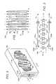
- FIG. 1is a block diagram of a PECVD apparatus in accordance with an embodiment of a present invention.
- FIG. 2is a perspective, cutaway view of a deposition chamber in accordance with an embodiment of a present invention.
- FIG. 3is a section view taken along line 3 - 3 in FIG. 2 .
- FIG. 4is a side view of rod electrodes in accordance with an embodiment of a present invention.
- FIG. 5is a simplified vertical cross sectional view of an exemplary barrier coating on an exemplary substrate in accordance with an embodiment of a present invention.
- Barrier film(s) and “barrier coating(s)”are used interchangeably herein to mean one or more inert passivation layers deposited on a substrate that stabilize the substrate, do not have an appreciable electrical effect on the substrate and substantially prevent moisture, oxygen, environmental pollutants, and other impurities or the like reaching the substrate.
- Substrateas used herein means the object being coated by the process under discussion. Those skilled in the art understand that, at the beginning of a given process, a “substrate” may be uncoated, or it may already have one or more coatings deposited on its surface by previous processes.
- solar cellsas used herein includes a single photovoltaic element for converting sunlight to electricity.
- solar panelsas used herein means a large area device that includes a plurality of solar cells, interconnected in series and/or parallel, to create a power generating device with large voltage and current capability.
- silicon based thin-film devicesinclude amorphous, crystalline or partially crystalline silicon solar cells and panels and flat panel displays, and other electronic devices that include a thin layer of amorphous, crystalline or partially crystalline silicon as part of their structure.
- thin film device(s)includes solar cells, solar panels and the terms “solar cells” and “solar panels” as used herein include “thin-film devices.” “Thin-film devices” also include window glass, flat panel displays, lenses, etc. and other large area substrates, silicon-based or not, that would benefit from a thin-film barrier coating. “Thin film device(s) as used herein may also include small area substrates that would benefit from a thin-film barrier coating such as wafer-based solar cells, optics or other semiconductor devices.
- a PECVD system 100in accordance with one embodiment of a present invention includes a deposition chamber 102 with an electrode assembly 104 between a pair of substrate carriers 106 a and 106 b .
- the substrate carriers 106 a and 106 bposition substrates on opposite sides of the electrode assembly 104 .
- the substratesare silicon based thin film devices such as solar panels as hereinafter described.
- the electrode assembly 104 in the exemplary implementationperforms a number of functions.
- the electrode assembly 104creates one or more high intensity plasma regions between the substrate carriers 106 a and 106 b when excited by a voltage, e.g. radio frequency (RF) or direct current (DC), provided by a power supply 108 .
- RFradio frequency
- DCdirect current
- alternate rod electrodesare excited with +RF and ⁇ RF so that the voltages on adjacent rod electrodes are out of phase with each other. This creates an intense plasma between the rod electrodes and a much weaker plasma out toward the substrates.
- the electrode assembly 104also contains channels to deliver reactant gas to the deposition chamber 102 and is connected to a reactant gas source 110 by way of a manifold 112 a . The gas is introduced into the chamber through apertures 134 in the rod electrodes. These apertures can be located on the surfaces closest to the substrates and away from the regions of intense plasma between the rod electrodes. In an alternate embodiment, they can be located on the surfaces that face the adjacent rod electrodes and inject the gas directly into the regions of intense plasma.
- the electrode assembly 104is used to evacuate exhaust from the deposition chamber 102 and, to that end, is connected to an exhaust device 114 , such as vacuum pump, by way of the manifold 112 b . Operation of the PECVD system 100 is monitored and controlled by a controller 116 , based at least in part on data from sensors 118 .
- the substrates 120 a and 120 benter the exemplary deposition chamber 102 by way of inlets 122 a and 122 b and travel in the direction indicated by arrows A. Similar outlets (not shown) are provided at the opposite end of the deposition chamber 102 .
- the substrates 120 a and 120 bmay be in the form of individual sheets of underlying material coated with amorphous, crystalline or partially crystalline silicon P-I-N layers along with metal conductor layer that are each fed into the deposition chamber 102 .
- the substratesmay also be a continuous web of underlying material coated with amorphous, crystalline or partially crystalline silicon P-I-N along with metal conductor layers that is pulled from a supply roll to a take-up roll.
- Suitable underlying materialsinclude, but are not limited to, soda-lime glass, polyimide, and stainless steel. Whether the underlying materials are in individual sheet or roll form, the substrate carriers 106 a and 106 b position the substrates 120 a and 120 b parallel to each other on opposite sides of the deposition chamber 102 and on opposite sides of the electrode assembly 104 .
- the substrate carriers 106 a and 106 balso include a plurality of roller units 124 and the edges of the substrates 120 a and 120 b pass between the rollers in the associated roller units.
- the rollers in the roller units 124may be free spinning rollers, which merely guide the substrates 120 a and 120 b through the deposition chamber 102 and ensure that they are properly positioned within the chamber.
- the roller units 124may include driven rollers that drive the substrates 120 a and 120 b through the deposition chamber 102 , in addition to ensuring that they are properly positioned.
- suitable substrate carriersinclude conveyor systems and chain drives.
- the substratescould be loaded into the chamber by a robot arm, held in place by sliding or roller guides and then removed from the chamber by the robot arm after the deposition is complete.
- Still another alternativeis to employ rollers that engage the top and bottom edges of the substrates 120 a and 120 b and rotate about axes that are perpendicular to the direction indicated by arrows A.
- the interior of the deposition chamber 102 in the exemplary embodimentis relatively narrow. More specifically, the distance between the substrates 120 a and 120 b is substantially less than the length of the chamber (measured in the direction of arrows A) and the height of the chamber (measured in the direction perpendicular to arrows A). For example, the distance between substrates 120 a and 120 b may be one-tenth or less of the length and height dimensions.
- the substrates 120 a and 120 bwill also preferably extend from end to end in the length dimension of the deposition chamber 102 and from top to bottom in the height dimension. As a result, the substrates 120 a and 120 b will be between the electrode assembly 104 (and the plasma created thereby) and the large interior surfaces of the chamber and will substantially cover the vast majority of the interior surface of the deposition chamber 102 .
- the deposition chamber 102is not limited to any particular size. Nevertheless, in one exemplary implementation of the deposition chamber 102 that is suitable for commercial applications and is oriented in the manner illustrated in FIG. 2 , the interior of the deposition chamber 102 is about 100 cm in length (measured in the direction of arrows A) and about 60 cm in height (measured in the direction perpendicular to arrows A). There is also about 7 cm between the substrates 120 a and 120 b and about 3.5 cm between the central plane CP of the deposition chamber interior ( FIG. 3 ) and each of the substrates 120 a and 120 b . Additionally, the substrate carriers 106 a and 106 b are positioned and arranged such that the substrates 120 a and 120 b will lie in vertically extending planes. Such orientation reduces the likelihood that particulates will fall onto the substrates.
- the relatively small spacing between the substrates 120 a and 120 bincreases the percentage of the plasma generated silicon nitride that is deposited onto the substrates and decreases the amount that is deposited onto the chamber walls, as compared to conventional deposition chambers.
- the reactant materialsare consumed more efficiently.
- the downtime and expense associated with deposition chamber cleaning and maintenanceis also reduced.
- the close spacing between the electrode assembly 104 and the substrates 120 a and 120 balso facilitates rapid diffusion in the smallest dimension as the dominant process for transporting atomic nitrogen created at the center of the deposition chamber 102 to the substrates, where the atomic nitrogen can react with silane to deposit SiN x onto the substrates.
- the configuration of the deposition chamber 102also allows rapid diffusion to equalize the concentrations of all species throughout the plasma, including the rapid diffusion of the input reactant gas, to obtain a uniform concentration.
- the exemplary electrode assembly 104 illustrated in FIGS. 2-4includes a plurality of spaced rod electrodes 126 arranged such that their respective longitudinal axes are co-planar, perpendicular to the direction of substrate travel (indicated by arrows A), and equidistant from the substrate carriers 106 a and 106 b (as well as substrates 120 a and 120 b ).
- the rod electrodes 126also extend from one end of the deposition chamber 102 to the other (top to bottom in the orientation illustrated in FIG. 2 ).
- the exemplary rod electrodes 126are cylindrical in shape and are relatively close together. The spacing between adjacent rod electrodes 126 in the illustrated embodiment is about equal to the diameter of the rod electrodes (i.e. two times the diameter measured from longitudinal axis to longitudinal axis).
- the electrode assembly 104may be used to create high intensity plasma between the substrate carriers 106 a and 106 b (as well as substrates 120 a and 120 b ).
- the high intensity plasmais created when the rod electrodes 126 are energized by power such as, for example, RF or DC power from the power supply 108 .
- the energyis supplied in alternating phases from one rod electrode 126 to the next adjacent rod electrode, as is represented by the alternating series of “+” and “ ⁇ ” signs in FIGS. 3 and 4 .
- the application of power in this mannercreates regions of high intensity electric field between adjacent rod electrodes 126 and, accordingly, regions of intense plasma 128 between adjacent rod electrodes.
- Low intensity electric fields and low intensity plasma regions 130are created near the substrates 120 a and 120 b . More specifically, in an exemplary implementation where adjacent rod electrodes 126 are spaced from one another by one rod diameter (i.e. two diameters from longitudinal axis to longitudinal axis) and the substrates spaced from the central plane CP by three and one-half rod electrode diameters, the intensity of the electric fields between the rod electrodes will be significantly greater than ten times the intensity of the electric field near the substrates 120 a and 120 b.
- the rod electrodes 126may, alternatively, be driven in phase with each other.
- the substrates 120 a and 120 bare held at ground potential or at ground with a small DC bias. This will create a relatively uniform electric field and plasma in each of the two areas between the central plane CP and the substrates 120 a and 120 b.
- the rod electrodes 126present a load having a capacitive reactance.
- the RF energyis coupled to the rod electrode in parallel with an inductive reactance so as to create a predominantly resonant circuit.
- the rod electrodesform a transmission line with a characteristic impedance similar to coaxial cables commonly used to transport RF energy from a RF power source to a load. As the length of the rod electrodes is increased and/or the RF frequency is increased, the length of the rod transmission line becomes comparable to 1 ⁇ 4 wavelength of the RF frequency.
- each rod electrode 126is preferably electrically driven at both longitudinal ends in order to reduce amplitude variations of the excitation signal along the length of the electrode. This minimizes the effects of standing waves at high RF frequencies and provides a relatively even plasma intensity along the length of each electrode.
- electrical contactsmay be provided to connect substrates 120 a and 120 b to the system ground, or to bias the substrates positive or negative with respect to the system ground, to control the plasma properties and the amount of electron/ion bombardment at the surface of the substrates. Magnetic fields may also be used to control plasma properties, i.e. confine the plasma and direct the movement of ions and electrons within the plasma.
- the rod electrodes 126 illustrated in FIGS. 2-4may be formed from a variety of materials that are relatively high in thermal and electrical conductivity to achieve a uniform electrical field and uniform temperature along the length of the rod.
- Material that is inert in a nitrogen plasma or oxidizing environment, such as titanium or stainless steel,may be used.
- the rod electrodes 126in one implementation that is suitable for commercial applications are cylindrical in shape, are about 1.2 cm in diameter and about 60 cm in length.
- the rod electrodes 126are positioned parallel to one another about every 2 cm (i.e. 2 cm between the longitudinal axes of adjacent rod electrodes) in the direction of substrate travel and in the central plane CP of the deposition chamber interior.
- the central plane CPis also the electrode plane. So configured and arranged, there will be forty eight of the rod electrodes 126 in a 100 cm long deposition chamber that has small electrode-free areas near the inlets and outlets.
- the rod electrodes 126are not, however, limited to these configurations and arrangements.
- the rod electrodesmay be other than circular in cross-sectional shape, as are the exemplary cylindrical rod electrodes 126 .
- the spacing between the rod electrodes 126will vary, where some or all of the rod electrodes are slightly offset from the central plane CP and/or where some of the rod electrodes are not parallel to others.
- the cross-sectional size of the rod electrodes(e.g. the diameter where the rod electrodes are cylindrical) may also be varied from electrode to electrode to suit particular applications.
- the arrangement of the plurality of closely spaced rod electrodes 126allows higher RF frequencies to be used to excite the plasma in the present PECVD system 100 , as compared to the frequencies that can be used in conventional PECVD systems, when the systems are of commercial production size (i.e. where the substrates are relatively long and at least 0.5 m wide).
- the series of parallel rod electrodes 126with alternating phases of applied RF power, forms a series of well characterized electronic transmission lines capable of supporting high frequency RF excitation in the range of 27-81 MHz. It has been shown in laboratory experiments that RF power in the 27-81 MHz excitation frequency range can provide higher deposition rates (i.e.
- the present electrode assembly 104produces well controlled standing waves and only minor variations in plasma intensity when excited to a frequency of 80 MHz over relatively long substrates that are at least 0.5 m wide.
- high intensity plasma regions 128 along the central plane CP ( FIG. 3 ) of the deposition chamber 102 and low intensity plasma regions 130 near the substrates 120 a and 120 bare associated with the creation of high intensity plasma regions 128 along the central plane CP ( FIG. 3 ) of the deposition chamber 102 and low intensity plasma regions 130 near the substrates 120 a and 120 b .
- the high intensity plasma regions 128generate abundant atomic nitrogen, which is known to encourage the formation of silicon nitride with good barrier properties. Atomic nitrogen generated in the central plane CP will diffuse easily to the substrates and unlike experimental systems that have been reported in PECVD-related literature, does not have to flow through a tube or other apparatus through which much of the atomic nitrogen would react and be lost.
- the high intensity plasma regions 128 in the central plane CP between the rod electrodes 126also generate intense UV photons that can easily flow to the substrates 120 a and 120 b .
- the UV photonscan flow to substrate without passing from outside the deposition chamber through a window or other apparatus.
- the presence of a window or similar componenthas the disadvantages of decreasing the photon intensity at the substrate and creating a significant maintenance issue when the window becomes degraded by color centers or other flaws formed or aggravated by UV absorption.
- the creation of low intensity plasma regions 130 near the substrates 120 a and 120 breduces the electron/ion bombardment of the substrates and potential damage to the deposited silicon nitride by electrons and/or ions.
- a series of rod electrodes that are arranged in the manner described abovedoes not create a uniform electric field and plasma in the substrate travel direction indicated by arrows A and, instead, will create an electric field and plasma that varies periodically in the travel direction from the area closet to a rod electrode to the midpoint between two rod electrodes.
- the deposition rate and barrier properties of the deposited materialcould, therefore, vary periodically in the travel direction.
- the illustrated embodimenteliminates this periodic variation in electric field and plasma intensity in a variety of ways. Periodic variations are reduced to a large extent by insuring that the distance between adjacent rod electrodes 126 , as well as the distance between the rod electrodes and the substrates 120 a and 120 b , is within a diffusion length.
- the spacing between adjacent rod electrodes 126is less than half of the distance from the central plane CP to the substrates.
- the spacing between adjacent rod electrodes 126 and from the rod electrodes to the substrates 120 a and 120 bshould be minimized so that rapid diffusion can further reduce variations in the deposition rate.
- the substrates 120 a and 120 bcan be moved relatively rapidly in the non-uniform direction (i.e. the direction indicated by arrows A) to average out any small, remaining variations in the deposition rate.
- the electrode assembly 104may, in some implementations of the present inventions, also be used during the deposition process to deliver reactant materials to the deposition chamber 102 and to evacuate exhaust from the deposition chamber.
- the rod electrodes 126include interior lumens 132 that are connected to the manifold 112 a (or 112 b ) and the apertures 134 that connect the interior lumens to the interior of the deposition chamber 102 .
- Each rod electrode 126includes two sets of apertures 134 , one set that faces the substrate 120 a and another set that faces the substrate 120 b .
- the interior lumens 126 in the illustrated embodimentare connected to the manifolds 112 a and 112 b such that, in the direction of substrate travel (i.e. the direction indicated by arrows A) the rod electrodes 126 alternate from one rod electrode to the next between delivering reactant materials and evacuating exhaust.
- the reactantsare represented by arrows R in FIGS. 3 and 4
- the exhaustis represented by arrows E.
- the manifold 112 aconnects the lumens 132 of the rod electrodes 126 that are delivering reactant material to the reactant gas source 110
- the manifold 112 bconnects the lumens of the rod electrodes that are evacuating exhaust to the exhaust device 114 .
- the manifolds 112 a and 112 bare also connected to both longitudinal ends of each of the associated rod electrodes 126 . As such, reactant materials enter both longitudinal ends of each of the rod electrodes 126 that are delivering reactant materials, and the exhaust exits both longitudinal ends of each of the rod electrodes that are evacuating exhaust.
- the exemplary lumens 132 in the illustrated embodimentare slightly smaller than the rod electrodes 126 .
- the lumen 132would be about 1.0 cm in diameter in a cylindrical rod electrode 126 that is itself 1.2 cm in diameter, and about 0.5 cm in diameter in a cylindrical rod electrode that is itself 0.6 cm in diameter.
- the apertures 134which are about 350 ⁇ m in diameter in the larger rod electrodes 126 and about 200 ⁇ m in diameter in the smaller rod electrodes, are positioned about every 0.5 cm along the length of the rod electrodes 126 .
- the apertures 134may also be aligned with one another from one rod electrode 126 to the next, or staggered, as applications require.
- supplying energy in alternating phases from one rod electrode 126 to the next adjacent rod electrodecreates high intensity plasma regions 128 and low intensity plasma regions 130 .
- the apertures 134are positioned so that they do not face the high intensity plasma regions 128 and, instead, face the low intensity plasma regions 130 .
- the apertures 134face in directions that are perpendicular to the central plane CP and are positioned on the portions of the rod electrodes 126 that are closest to the substrates 120 a and 120 b .
- the angle of the apertures 134 relative to the central plane CPmay, however, be adjusted as applications require.
- the anglemay be up to forty-five (45) degrees from perpendicular. Because the reactant material, i.e. silane in the exemplary implementation, is introduced into the low intensity plasma regions 130 , the silane rapidly diffuses and dilutes itself into the nitrogen atmosphere inside the chamber before encountering regions of intense plasma 128 . This reduces the formation of higher order silanes and/or silicon particles within the plasma.
- the reactant materiali.e. silane in the exemplary implementation
- the reactant gas source 110may be used to fill the deposition chamber 102 with ammonia or nitrogen, or a mixture of ammonia, nitrogen and argon (Ar), at the desired pressure (e.g. 50 mTorr) prior to the excitation of the rod electrodes 126 and the introduction of the silane or other reactant material.
- the rod electrodes 126are then excited to initiate the plasma.
- the reactant gas source 110supplies pure or highly concentrated silane to the rod electrodes 126 that are supplying reactants by way of the manifold 112 a .
- the apertures 134direct the pure silane into the low intensity plasma regions 130 and the silane diffuses rapidly (i.e.
- the diffusionoccurs before the silane reaches the high intensity plasma regions 128 where the silane is consumed by the decomposition into silicon and hydrogen (SiH 4 ⁇ Si+2H 2 ).
- the rapid diffusion and dilution into the nitrogen atmosphere with the deposition chamber 102 prior to encountering high intensity plasma regions 128 , as well as the relatively short rod electrode to adjacent rod electrode distance that the silane travels and correspondingly short residence time within the deposition chamberalso reduces the formation of higher order silanes (Si 2 H 6 , Si 3 H 8 , etc.) and/or silicon particles within the plasma.
- the silicon nitrideis deposited onto the substrates 120 a and 120 b , while the hydrogen and a very small amount of unused silane is removed by the apertures 134 in the other rod electrodes 126 and the exhaust device 114 .
- the overall reaction for silicon nitride deposition in the PECVD process using silane and ammoniacan be written as follows:
- the flow of silane and the powerare carefully controlled to set the deposition rates. Nitrogen from ammonia is abundant in the chamber and does not limit the deposition rates.
- both silane and ammoniacan be introduced into the chamber through the apertures 134 in the rod electrodes. This arrangement could be used to control the ratio of NH 3 and silane to be close to 4:3 as in the chemical reaction shown above, if desired.
- SiN x H yis obtained as the final product.
- Hydrogen containing SiN x H yis a good passivation layer for numerous applications. Hydrogen content depends upon several factors depending upon SiH 4 to NH 3 flow ratio, effective dissociation and utilization of SiH 4 , and the substrate temperature. In general in PECVD process, the free radicals generated by the plasma environment activate the chemical reaction at lower temperatures than thermal chemical vapor deposition.
- high frequencyleads to higher ionization which in turns leads to intensive dissociation of silane (SiH 4 ) and ammonia (NH 3 ).
- High ionizationprovides enough N atoms to consume all of the dissociated silane.
- High frequencywill also allow the use of lower pressure thereby minimizing the particulate contaminants.
- High frequencyreduces ion energy due to decrease in sheat voltage leading to a lower impact on the substrate by the ions.
- the input flow rate of the pure silaneneeds to be only slightly greater than the rate at which the silane is consumed because only a small amount of the silane is wasted. More specifically, when the gas in the deposition chamber reaches the apertures 134 in the rod electrodes 126 that are being used to evacuate exhaust from the deposition chamber 102 , the concentration of silane can be very small.
- the exhaust gas flow rateshould be several times the input gas flow rate in order to maintain a constant pressure in the deposition chamber 102 . All of the hydrogen generated in the deposition reaction is removed by the exhaust. Hence a high percentage of the silane is used in the deposition process.
- Conventional PECVD systemsconvert only about 5-10% of the silane into silicon nitride and the remainder is wasted. Of course, in conventional PECVD systems and the present PECVD system 100 , some of the silicon nitride is deposited onto the walls of the deposition chamber. This brings conventional PECVD systems down to about 5% utilization efficiency, i.e.
- the geometry of the present deposition chamber 102reduces the percentage of deposits onto the walls of the deposition chamber and, accordingly, the overall utilization efficiency of the present PECVD system 100 is about 50% and higher.
- Another advantage associated with the supply of pure silane through some of the rod electrodes 126 and the evacuation of exhaust through othersis that it facilitates much lower gas flow rates than conventional PECVD systems.
- the lower flow ratesallow for a much lower capacity exhaust device 114 (e.g. vacuum pump) to be used to evacuate the reaction products from the deposition chamber 102 and maintain a constant chamber pressure.
- the very short travel distance from a rod electrode 126 that is supplying reactant to a rod electrode that is evacuating exhauste.g. substantially less than one-twentieth ( 1/20) of the length and/or height of the deposition chamber 102 in the illustrated embodiment
- the short dwell timeminimizes the formation of high order silanes and/or silicon particles.
- the rod electrodes 126are driven in phase with each other, and the substrates 120 a and 120 b held at ground potential (or at ground with a small DC bias), to create a relatively uniform electric field and plasma in each of the two areas between the central plane CP and the substrates.
- the rod electrodes 126may be rotated ninety (90) degrees from the orientation illustrated in FIG. 3 so that the apertures 134 are facing adjacent rod electrodes and reactant is supplied to, and exhaust is evacuated from, the region where the electrical field is minimized.
- This implementation of the inventionsalso benefits from the very short travel distance from a rod electrode 126 that is supplying reactant to a rod electrode that is evacuating exhaust in that the dwell time for silane in the reaction chamber 102 is short, even though the flow rates are low, and the short dwell time minimizes the formation of high order silanes and/or silicon particles.
- the reactant gas source 110which may be used to supply the deposition chamber 102 with silane and ammonia during the deposition process, includes a plurality of storage containers G 1 -G N .
- Other gasses that may be storedinclude argon, nitrogen, hydrogen, oxygen, methane, acetylene.
- the gassesmay be stored under pressure and, to that end, the reactant gas source 110 includes a plurality of valves 136 that control the flow rate of the gasses from the storage containers G 1 -G N .
- the present inventionsare not limited to gaseous reactant material. Sources of liquid and/or solid reactants may also be provided if required by particular processes.
- the ammoniagenerates atomic nitrogen and atomic hydrogen
- the nitrogengenerates atomic nitrogen
- the oxygengenerates atomic oxygen
- the methane and acetylenegenerate carbon radicals and atomic hydrogen with application of high frequency RF power.
- the controller 116may be used to control a variety of aspects of the deposition process. For example, the rate at which pure silane is supplied to the deposition chamber 102 and the rate at which exhaust is evacuated from the deposition chamber may be controlled based upon data from the sensors 118 . As noted above, the silane input rate should be slightly greater than the rate at which the silane is consumed (i.e. the deposition rate) because only a small amount of the silane is wasted. Thus, for a particular deposition rate and power level applied to the rod electrodes 126 by the power supply 108 (or “plasma power”), the input flow rate may be adjusted by feedback from the sensors 118 to achieve the desired concentration of silane in the exhaust gas.
- the exhaust gas concentration of silanewill typically be about 5%.
- the input flow rate of the silaneis adjusted to be equal to the rate consumed in the deposition and the concentration of silane in the exhaust gas approaches zero.
- the exhaust rateis also controlled by feedback to maintain the pressure in the deposition chamber 102 at the desired pressure (e.g. about 10-1000 mTorr, preferably about 50 mTorr).
- the temperature of the substrates 120 a and 120 b and the frequency and power level of the plasma excitationwill also typically be controlled to achieve the desired quality of silicon at the desired deposition rate.
- the sensors 118may include a gas concentration sensor associated with the exhaust device 114 , a pressure sensor within the deposition chamber 102 , and a temperature sensor associated with the substrates 120 a and 120 b .
- a sensor that detects the presence of a plasma to verify correct operationmay also be provided.
- Controlling the PECVD process in the manner described aboveallows the present PECVD system to perform continuous deposition processes at a stable, steady state with stable temperature, gas flow, gas concentrations, deposition rates, etc.
- the controller 116can use feedback from the sensors 118 to adjust the parameters of the stable, steady state and achieve the desired material properties.
- the combination of steady state operation and parameter adjustment, based on sensors within the system as the deposition process proceeds, together with rapid diffusion to reduce any non-uniformityallows the manufacture of the present system to be much less precise in mechanical tolerances, and less uniform in gas flow. As a result, the present system can be manufactured much less expensively than conventional “batch mode” systems which deposit material with comparable uniformity and semiconducting properties.
- FIG. 5illustrates an exemplary solar cell with a barrier coating deposited according to the inventive method.
- Substrate 138is a solar cell made by depositing a functional film stack 140 on an underlying material 142 .
- Barrier coating 144comprises passivation layers 144 a and 144 b , which may be of identical or different compositions.
- Those skilled in the artwill recognize that a variety of other coatings, deposited on a variety of other coated or uncoated substrates, are within the scope of the invention if the deposition is performed according to the inventive method.
- the present PECVD system 100may be used to produce a variety of material layers. Although the inventions are described in the context of the formation of thin films of silicon nitride (SiNx) from silane (SiH 4 ) and ammonia (NH 3 ), they are not limited to any particular types of films or input reactant material. By way of example, but not limitation, the PECVD system 100 may be used to form silicon nitride, silicon oxide, silicon carbide, titanium carbide, and other layers on large substrates (e.g. 1 m ⁇ 0.5 m) that may be utilized in silicon thin film photovoltaic cells and other large area, low cost thin-film devices.
- large substratese.g. 1 m ⁇ 0.5 m
- barrier coatings for silicon based thin film deviceshave been described, it is to be appreciated that substantial benefit may be achieving by using this method to deposit barrier coatings on window glass, flat panel displays, lenses, etc and other large area substrates that would benefit from a thin-film barrier coating.
- deposition of barrier coatings on large area substrateshas been described and is particularly advantageous, it is to be appreciated that the inventive method may also be used to deposit barrier coatings on small area substrates.
- the inventive PECVD process for depositing barrier coating layers on substrateshas a number of advantages as compared to conventional PECVD process. These advantages include a high deposition rate (5 nm/sec), low substrate temperature (less than about 150 degrees Celsius, preferably about 100° C.), less particulate formation, effective silane (SiH 4 ) utilization due to close proximity of the precursor injection, and substantially uniform deposition due to the multitubular injection manifold design.
- the processis particularly advantageous for depositing a barrier coating on large area substrates (1 m ⁇ 0.5 m and larger)
Landscapes
- Physics & Mathematics (AREA)
- Engineering & Computer Science (AREA)
- Plasma & Fusion (AREA)
- Chemical & Material Sciences (AREA)
- Electromagnetism (AREA)
- Spectroscopy & Molecular Physics (AREA)
- General Chemical & Material Sciences (AREA)
- Chemical Kinetics & Catalysis (AREA)
- Materials Engineering (AREA)
- Mechanical Engineering (AREA)
- Metallurgy (AREA)
- Organic Chemistry (AREA)
- Chemical Vapour Deposition (AREA)
Abstract
Description
- The present application is a continuation-in-part of U.S. patent application entitled “PLASMA ENHANCED CHEMICAL VAPOR DEPOSITION APPARATUS AND METHOD”, Ser. No. 11/553,334 filed Oct. 26, 2006 and having at least one common inventor and assigned to the same assignee which claims priority to PCT/US2004/030275, herein incorporated by reference. This application is also related to application Ser. No. 11/420,429, filed May 25, 2006 and to U.S. Pat. No. 7,264,849 issued Sep. 4, 2007 both entitled “Roll-Vortex Plasma Chemical Vapor Deposition System” by at least one common inventor and assigned to the same assignee and herein incorporated herein by reference.
- This invention relates generally to a method for producing barrier coatings using a high frequency plasma enhanced chemical vapor deposition (PECVD) process. More specifically, this invention relates to barrier coating deposition on large area thin film devices such as silicon photovoltaic cells.
- PECVD is a well known technology in various industries (such as semiconductor, data storage, photovoltaic, flat panel display, and packaging) for thin film deposition on a variety of materials. Plasma is an ionized form of gas that can be obtained by ionizing a gas or liquid medium using an AC or DC electric field. Typically in a PECVD process, reactant precursors are excited and dissociated in the reaction zone by applying radio frequency energy to the reactants. The reactive species react at a substrate surface for the completion of the reaction. Highly reactive species involved in the chemical reaction scheme at the substrate allow lower temperatures for the completion of the reaction at high reaction rates. Reaction rates are enhanced by increasing the degree of ionization in the plasma chamber. High frequencies (27-81 MHz) form plasma with higher ionization density leading to high deposition rate with lower hydrogen content in the deposited film thereby decreasing the need for high temperature of the substrates. Keeping the substrate temperature low is a must for some applications where high temperatures can degrade the performance of the materials already deposited on the substrate
- As described in U.S. Pat. No. 7,264,849 issued Sep. 4, 2007, entitled “Roll-Vortex Plasma Chemical Vapor Deposition System,” and Plasma Enhanced Chemical Vapor Deposition Apparatus and Method, application Ser. No. 11/553,334 filed Oct. 26, 2006, co-owned and incorporated herein by reference, the PECVD process is capable of producing high quality amorphous silicon thin film devices for the photovoltaic industry at a high deposition rate. This patent and patent application describe incorporating several tubular electrodes in the deposition chamber, operated at high frequency 27-81 MHz to provide a uniform deposition of high quality amorphous silicon film at a high deposition rate on a large size solar panel.
- For such large area thin film solar panels, there is a need to protect the solar panels from moisture, oxygen, environmental pollutants, and other impurities. In the semiconductor industry, the use of barrier coatings to seal and protect solar panels is often referred to as “passivation”. For example, Si3N4is a commonly used barrier coating and is often referred to as a “passivation layer” or “passivation film.” A barrier coating may be a single passivation layer or a stack of multiple passivation layers with identical or different compositions. The protective barrier coating for a solar cell or panel, for example, must be insulating with high dielectric strength, pore free, continuous, and conformal, covering various step heights on the panel.
- PECVD processes have been used to produce barrier coatings for different applications. Examples of PECVD systems to deposit barrier coatings (such as silicon nitride) are described in U.S. Pat. Nos. 6,924,241; 5,418,019; 4,253,881; 6,150,286; 6,664,202; 6,756,324; 6,720,249; 6,984,893; 6,686,232; 4,563,367. For example, U.S. Pat. No. 6,924,241 describes a PECVD process operating at 13.56 MHz to produce an ultraviolet light (UV) transmissive silicon nitride layer. The process reduces the concentration of Si—H bonds in the silicon nitride film to provide UV transmissivity. The film may be used as a passivation layer in a UV erasable memory integrated circuit. The reactor used in this patent is a CONCEPT ONE dual-frequency parallel plate PECVD reactor from Novellus Systems, Inc.
- Another example is U.S. Pat. No. 6,664,202, where a mixed frequency PECVD process is utilized to create high quality silicon nitride layer having high conformality. In a mixed frequency PECVD process, both high and low frequency RF energy (e.g. one 13.56 MHz and one signal less than 1 MHz) is applied to one or more electrodes positioned near the reaction zone.
- U.S. Pat. No. 5,418,019 describes a method for low temperature plasma enhanced chemical vapor deposition of SiN and SiO2antireflective coating on silicon. A PECVD reactor developed by Plasma-Therm (series700) was used to deposit these films at 13.56 MHz RF power range. The substrate temperature was 300° C. in this deposition.
- Silicon nitride is a good insulating material to be used as a barrier-coating passivation layer on the thin film solar cell. Silicon nitride (Si3N4) is known for its barrier properties to moisture, oxygen and environmental pollutants and is used as a barrier coating in semiconductor, data storage and packaging industries. Typically, silicon nitride is deposited either by reactive sputtering or by plasma enhanced chemical vapor deposition (PECVD) processes. Plasma enhanced chemical vapor deposition is a more attractive method than reactive sputtering due to its higher deposition rates and better conformality of the deposition. Typical silicon nitride deposition using PECVD is done at temperatures ˜300° C.
- However, for passivation of silicon based thin film solar panels, the barrier coating must be applied at low temperature (<150° C.) to avoid degradation (at the p-i interface) of the semiconductor films already deposited on the substrate. Low temperatures, however, often lead to more particulate formation, which is undesirable.
- There is therefore a need for a novel PECVD process for depositing barrier coatings on substrates with a high deposition rate (5 nm/sec), at low substrate temperature, and with less particulate formation over conventional PECVD processes. There is also a need for a novel PECVD process that has effective silane (SiH4) utilization, deposition uniformity, and good for depositing barrier coatings on large area substrates (1 m×0.5 m and larger). The present invention fulfills these needs and provides other related advantages.
- The primary objective of this invention is to produce barrier coatings, which passivation-layer compositions may include SiNx, SiO2, SiC or the like for solar cell passivation using a high frequency (27-81 MHz) plasma enhanced chemical vapor deposition process. This PECVD process provides a substantially uniform deposition of barrier coatings at a high deposition rate on a large area thin film devices at low temperature (less than about 150 degrees Celsius, preferably about 100° C.).
FIG. 1 is a block diagram of a PECVD apparatus in accordance with an embodiment of a present invention.FIG. 2 is a perspective, cutaway view of a deposition chamber in accordance with an embodiment of a present invention.FIG. 3 is a section view taken along line3-3 inFIG. 2 .FIG. 4 is a side view of rod electrodes in accordance with an embodiment of a present invention.FIG. 5 is a simplified vertical cross sectional view of an exemplary barrier coating on an exemplary substrate in accordance with an embodiment of a present invention.- The following is a detailed description of the best presently known modes of carrying out the inventions. This description is not to be taken in a limiting sense, but is made merely for the purpose of illustrating the general principles of the inventions. It should also be noted that detailed discussions of the various aspects of PECVD systems that are not pertinent to the present inventions have been omitted for the sake of simplicity.
- “Barrier film(s)” and “barrier coating(s)” are used interchangeably herein to mean one or more inert passivation layers deposited on a substrate that stabilize the substrate, do not have an appreciable electrical effect on the substrate and substantially prevent moisture, oxygen, environmental pollutants, and other impurities or the like reaching the substrate.
- “Substrate” as used herein means the object being coated by the process under discussion. Those skilled in the art understand that, at the beginning of a given process, a “substrate” may be uncoated, or it may already have one or more coatings deposited on its surface by previous processes.
- The term “solar cells” as used herein includes a single photovoltaic element for converting sunlight to electricity.
- The term “solar panels” as used herein means a large area device that includes a plurality of solar cells, interconnected in series and/or parallel, to create a power generating device with large voltage and current capability.
- The term “silicon based thin-film devices” as used herein include amorphous, crystalline or partially crystalline silicon solar cells and panels and flat panel displays, and other electronic devices that include a thin layer of amorphous, crystalline or partially crystalline silicon as part of their structure.
- The term “thin film device(s)” as used herein includes solar cells, solar panels and the terms “solar cells” and “solar panels” as used herein include “thin-film devices.” “Thin-film devices” also include window glass, flat panel displays, lenses, etc. and other large area substrates, silicon-based or not, that would benefit from a thin-film barrier coating. “Thin film device(s) as used herein may also include small area substrates that would benefit from a thin-film barrier coating such as wafer-based solar cells, optics or other semiconductor devices.
- As illustrated for example in
FIG. 1 , aPECVD system 100 in accordance with one embodiment of a present invention includes adeposition chamber 102 with anelectrode assembly 104 between a pair ofsubstrate carriers substrate carriers electrode assembly 104. In a preferred embodiment, the substrates are silicon based thin film devices such as solar panels as hereinafter described. Theelectrode assembly 104 in the exemplary implementation performs a number of functions. Theelectrode assembly 104 creates one or more high intensity plasma regions between thesubstrate carriers power supply 108. In one embodiment, alternate rod electrodes are excited with +RF and −RF so that the voltages on adjacent rod electrodes are out of phase with each other. This creates an intense plasma between the rod electrodes and a much weaker plasma out toward the substrates. Theelectrode assembly 104 also contains channels to deliver reactant gas to thedeposition chamber 102 and is connected to areactant gas source 110 by way of a manifold112a. The gas is introduced into the chamber throughapertures 134 in the rod electrodes. These apertures can be located on the surfaces closest to the substrates and away from the regions of intense plasma between the rod electrodes. In an alternate embodiment, they can be located on the surfaces that face the adjacent rod electrodes and inject the gas directly into the regions of intense plasma. During the deposition process, plasma is created in the area between substrates that are carried by thesubstrate carriers electrode assembly 104 is used to evacuate exhaust from thedeposition chamber 102 and, to that end, is connected to anexhaust device 114, such as vacuum pump, by way of the manifold112b. Operation of thePECVD system 100 is monitored and controlled by acontroller 116, based at least in part on data fromsensors 118. - Turning to
FIGS. 2-4 , thesubstrates exemplary deposition chamber 102 by way ofinlets deposition chamber 102. Thesubstrates deposition chamber 102. The substrates may also be a continuous web of underlying material coated with amorphous, crystalline or partially crystalline silicon P-I-N along with metal conductor layers that is pulled from a supply roll to a take-up roll. Suitable underlying materials include, but are not limited to, soda-lime glass, polyimide, and stainless steel. Whether the underlying materials are in individual sheet or roll form, thesubstrate carriers substrates deposition chamber 102 and on opposite sides of theelectrode assembly 104. Thesubstrate carriers roller units 124 and the edges of thesubstrates roller units 124 may be free spinning rollers, which merely guide thesubstrates deposition chamber 102 and ensure that they are properly positioned within the chamber. Alternatively, theroller units 124 may include driven rollers that drive thesubstrates deposition chamber 102, in addition to ensuring that they are properly positioned. Other suitable substrate carriers include conveyor systems and chain drives. Alternatively, the substrates could be loaded into the chamber by a robot arm, held in place by sliding or roller guides and then removed from the chamber by the robot arm after the deposition is complete. Still another alternative is to employ rollers that engage the top and bottom edges of thesubstrates - The interior of the
deposition chamber 102 in the exemplary embodiment is relatively narrow. More specifically, the distance between thesubstrates substrates substrates deposition chamber 102 and from top to bottom in the height dimension. As a result, thesubstrates deposition chamber 102. - The
deposition chamber 102 is not limited to any particular size. Nevertheless, in one exemplary implementation of thedeposition chamber 102 that is suitable for commercial applications and is oriented in the manner illustrated inFIG. 2 , the interior of thedeposition chamber 102 is about 100 cm in length (measured in the direction of arrows A) and about 60 cm in height (measured in the direction perpendicular to arrows A). There is also about 7 cm between thesubstrates FIG. 3 ) and each of thesubstrates substrate carriers substrates - There are a number of advantages associated with deposition chambers that are configured in this manner. For example, the relatively small spacing between the
substrates electrode assembly 104 and thesubstrates deposition chamber 102 to the substrates, where the atomic nitrogen can react with silane to deposit SiNxonto the substrates. The configuration of thedeposition chamber 102 also allows rapid diffusion to equalize the concentrations of all species throughout the plasma, including the rapid diffusion of the input reactant gas, to obtain a uniform concentration. - The
exemplary electrode assembly 104 illustrated inFIGS. 2-4 includes a plurality of spacedrod electrodes 126 arranged such that their respective longitudinal axes are co-planar, perpendicular to the direction of substrate travel (indicated by arrows A), and equidistant from thesubstrate carriers substrates rod electrodes 126 also extend from one end of thedeposition chamber 102 to the other (top to bottom in the orientation illustrated inFIG. 2 ). Theexemplary rod electrodes 126 are cylindrical in shape and are relatively close together. The spacing betweenadjacent rod electrodes 126 in the illustrated embodiment is about equal to the diameter of the rod electrodes (i.e. two times the diameter measured from longitudinal axis to longitudinal axis). - With respect to plasma formation, the
electrode assembly 104 may be used to create high intensity plasma between thesubstrate carriers substrates rod electrodes 126 are energized by power such as, for example, RF or DC power from thepower supply 108. The energy is supplied in alternating phases from onerod electrode 126 to the next adjacent rod electrode, as is represented by the alternating series of “+” and “−” signs inFIGS. 3 and 4 . The application of power in this manner creates regions of high intensity electric field betweenadjacent rod electrodes 126 and, accordingly, regions ofintense plasma 128 between adjacent rod electrodes. Low intensity electric fields and lowintensity plasma regions 130 are created near thesubstrates adjacent rod electrodes 126 are spaced from one another by one rod diameter (i.e. two diameters from longitudinal axis to longitudinal axis) and the substrates spaced from the central plane CP by three and one-half rod electrode diameters, the intensity of the electric fields between the rod electrodes will be significantly greater than ten times the intensity of the electric field near thesubstrates - It should be noted that the
rod electrodes 126 may, alternatively, be driven in phase with each other. Here, thesubstrates substrates - If the deposition chamber and rod electrodes are short compared with a ¼ wavelength at the excitation frequency, then the
rod electrodes 126 present a load having a capacitive reactance. The RF energy is coupled to the rod electrode in parallel with an inductive reactance so as to create a predominantly resonant circuit. However, the rod electrodes form a transmission line with a characteristic impedance similar to coaxial cables commonly used to transport RF energy from a RF power source to a load. As the length of the rod electrodes is increased and/or the RF frequency is increased, the length of the rod transmission line becomes comparable to ¼ wavelength of the RF frequency. In this case, the rod electrode is driven from each end with the appropriate value of inductance or capacitance to resonate it and effectively create a maximum voltage at the center of the rod electrode and a smaller voltage towards each end. In the embodiment ofFIGS. 3 and 4 , eachrod electrode 126 is preferably electrically driven at both longitudinal ends in order to reduce amplitude variations of the excitation signal along the length of the electrode. This minimizes the effects of standing waves at high RF frequencies and provides a relatively even plasma intensity along the length of each electrode. Additionally, electrical contacts (not shown) may be provided to connectsubstrates - With respect to materials, the
rod electrodes 126 illustrated inFIGS. 2-4 may be formed from a variety of materials that are relatively high in thermal and electrical conductivity to achieve a uniform electrical field and uniform temperature along the length of the rod. Material that is inert in a nitrogen plasma or oxidizing environment, such as titanium or stainless steel, may be used. - Turning to size and shape, the
rod electrodes 126 in one implementation that is suitable for commercial applications are cylindrical in shape, are about 1.2 cm in diameter and about 60 cm in length. Therod electrodes 126 are positioned parallel to one another about every 2 cm (i.e. 2 cm between the longitudinal axes of adjacent rod electrodes) in the direction of substrate travel and in the central plane CP of the deposition chamber interior. Thus, in the illustrated embodiment, the central plane CP is also the electrode plane. So configured and arranged, there will be forty eight of therod electrodes 126 in a 100 cm long deposition chamber that has small electrode-free areas near the inlets and outlets. - The
rod electrodes 126 are not, however, limited to these configurations and arrangements. For example, the rod electrodes may be other than circular in cross-sectional shape, as are the exemplarycylindrical rod electrodes 126. There may also be instances where the spacing between therod electrodes 126 will vary, where some or all of the rod electrodes are slightly offset from the central plane CP and/or where some of the rod electrodes are not parallel to others. The cross-sectional size of the rod electrodes (e.g. the diameter where the rod electrodes are cylindrical) may also be varied from electrode to electrode to suit particular applications. - There are a number of advantages associated with the
present electrode assembly 104. For example, the arrangement of the plurality of closely spacedrod electrodes 126 allows higher RF frequencies to be used to excite the plasma in thepresent PECVD system 100, as compared to the frequencies that can be used in conventional PECVD systems, when the systems are of commercial production size (i.e. where the substrates are relatively long and at least 0.5 m wide). The series ofparallel rod electrodes 126, with alternating phases of applied RF power, forms a series of well characterized electronic transmission lines capable of supporting high frequency RF excitation in the range of 27-81 MHz. It has been shown in laboratory experiments that RF power in the 27-81 MHz excitation frequency range can provide higher deposition rates (i.e. about 5 nm/sec.) and better material quality than the conventional excitation frequency of 13.5 MHz. Conventional electrode designs are not conducive to these higher frequencies in commercial production sized systems because they create poorly controlled standing waves, which results in non-uniform plasma intensity and non-uniform deposition rates. Conversely, thepresent electrode assembly 104 produces well controlled standing waves and only minor variations in plasma intensity when excited to a frequency of 80 MHz over relatively long substrates that are at least 0.5 m wide. - Other advantages are associated with the creation of high
intensity plasma regions 128 along the central plane CP (FIG. 3 ) of thedeposition chamber 102 and lowintensity plasma regions 130 near thesubstrates intensity plasma regions 128 generate abundant atomic nitrogen, which is known to encourage the formation of silicon nitride with good barrier properties. Atomic nitrogen generated in the central plane CP will diffuse easily to the substrates and unlike experimental systems that have been reported in PECVD-related literature, does not have to flow through a tube or other apparatus through which much of the atomic nitrogen would react and be lost. The highintensity plasma regions 128 in the central plane CP between therod electrodes 126 also generate intense UV photons that can easily flow to thesubstrates intensity plasma regions 130 near thesubstrates - It should also be noted that a series of rod electrodes that are arranged in the manner described above does not create a uniform electric field and plasma in the substrate travel direction indicated by arrows A and, instead, will create an electric field and plasma that varies periodically in the travel direction from the area closet to a rod electrode to the midpoint between two rod electrodes. The deposition rate and barrier properties of the deposited material could, therefore, vary periodically in the travel direction. The illustrated embodiment eliminates this periodic variation in electric field and plasma intensity in a variety of ways. Periodic variations are reduced to a large extent by insuring that the distance between
adjacent rod electrodes 126, as well as the distance between the rod electrodes and thesubstrates adjacent rod electrodes 126, is less than half of the distance from the central plane CP to the substrates. In fact, the spacing betweenadjacent rod electrodes 126 and from the rod electrodes to thesubstrates substrates - The
electrode assembly 104 may, in some implementations of the present inventions, also be used during the deposition process to deliver reactant materials to thedeposition chamber 102 and to evacuate exhaust from the deposition chamber. To that end, and referring toFIGS. 3 and 4 , therod electrodes 126 includeinterior lumens 132 that are connected to the manifold112a(or112b) and theapertures 134 that connect the interior lumens to the interior of thedeposition chamber 102. Eachrod electrode 126 includes two sets ofapertures 134, one set that faces thesubstrate 120aand another set that faces thesubstrate 120b. Theinterior lumens 126 in the illustrated embodiment are connected to themanifolds rod electrodes 126 alternate from one rod electrode to the next between delivering reactant materials and evacuating exhaust. The reactants are represented by arrows R inFIGS. 3 and 4 , while the exhaust is represented by arrows E. More specifically, the manifold112aconnects thelumens 132 of therod electrodes 126 that are delivering reactant material to thereactant gas source 110 and the manifold112bconnects the lumens of the rod electrodes that are evacuating exhaust to theexhaust device 114. Themanifolds rod electrodes 126. As such, reactant materials enter both longitudinal ends of each of therod electrodes 126 that are delivering reactant materials, and the exhaust exits both longitudinal ends of each of the rod electrodes that are evacuating exhaust. - The
exemplary lumens 132 in the illustrated embodiment are slightly smaller than therod electrodes 126. For example, thelumen 132 would be about 1.0 cm in diameter in acylindrical rod electrode 126 that is itself 1.2 cm in diameter, and about 0.5 cm in diameter in a cylindrical rod electrode that is itself 0.6 cm in diameter. Theapertures 134, which are about 350 μm in diameter in thelarger rod electrodes 126 and about 200 μm in diameter in the smaller rod electrodes, are positioned about every 0.5 cm along the length of therod electrodes 126. However, for both therod electrodes 126 delivering reactant materials and the rod electrodes evacuating exhaust, there is preferably a slight variation in aperture spacing from the longitudinal ends of therod electrodes 126 to the centers in order to compensate for the pressure drop that occurs between the longitudinal ends, which are connected to the manifold112a, and the center. More specifically, for 0.6 cmdiameter rod electrodes 126 with 200um apertures 134, there is about 5% less spacing at the center (i.e. about 0.475 cm spacing) and about 5% more spacing at the longitudinal ends (i.e. about 0.525 cm spacing) and the change occurs linearly. This results in a uniform flow rate through theapertures 134 in therod electrodes 126 from one longitudinal end of therod electrodes 126 to the other. Theapertures 134 may also be aligned with one another from onerod electrode 126 to the next, or staggered, as applications require. - As discussed above with reference to
FIGS. 3 and 4 , supplying energy in alternating phases from onerod electrode 126 to the next adjacent rod electrode (as represented by the “+” and “−” signs) creates highintensity plasma regions 128 and lowintensity plasma regions 130. Theapertures 134 are positioned so that they do not face the highintensity plasma regions 128 and, instead, face the lowintensity plasma regions 130. In the exemplary implementation, theapertures 134 face in directions that are perpendicular to the central plane CP and are positioned on the portions of therod electrodes 126 that are closest to thesubstrates apertures 134 relative to the central plane CP may, however, be adjusted as applications require. For example, the angle may be up to forty-five (45) degrees from perpendicular. Because the reactant material, i.e. silane in the exemplary implementation, is introduced into the lowintensity plasma regions 130, the silane rapidly diffuses and dilutes itself into the nitrogen atmosphere inside the chamber before encountering regions ofintense plasma 128. This reduces the formation of higher order silanes and/or silicon particles within the plasma. - The
reactant gas source 110 may be used to fill thedeposition chamber 102 with ammonia or nitrogen, or a mixture of ammonia, nitrogen and argon (Ar), at the desired pressure (e.g. 50 mTorr) prior to the excitation of therod electrodes 126 and the introduction of the silane or other reactant material. Therod electrodes 126 are then excited to initiate the plasma. During the actual deposition process, thereactant gas source 110 supplies pure or highly concentrated silane to therod electrodes 126 that are supplying reactants by way of the manifold112a. Theapertures 134 direct the pure silane into the lowintensity plasma regions 130 and the silane diffuses rapidly (i.e. within a few milliseconds) into the nitrogen (ammonia or mixture) already in thedeposition chamber 102. The diffusion occurs before the silane reaches the highintensity plasma regions 128 where the silane is consumed by the decomposition into silicon and hydrogen (SiH4→Si+2H2). The rapid diffusion and dilution into the nitrogen atmosphere with thedeposition chamber 102 prior to encountering highintensity plasma regions 128, as well as the relatively short rod electrode to adjacent rod electrode distance that the silane travels and correspondingly short residence time within the deposition chamber, also reduces the formation of higher order silanes (Si2H6, Si3H8, etc.) and/or silicon particles within the plasma. The silicon nitride is deposited onto thesubstrates apertures 134 in theother rod electrodes 126 and theexhaust device 114. As an example, the overall reaction for silicon nitride deposition in the PECVD process using silane and ammonia can be written as follows:
3SiH4+4NH3=Si3N4+12H2- In the embodiment detailed above, the flow of silane and the power are carefully controlled to set the deposition rates. Nitrogen from ammonia is abundant in the chamber and does not limit the deposition rates. In an alternate embodiment, both silane and ammonia can be introduced into the chamber through the
apertures 134 in the rod electrodes. This arrangement could be used to control the ratio of NH3and silane to be close to 4:3 as in the chemical reaction shown above, if desired. - Under PECVD conditions, SiNxHyis obtained as the final product. Hydrogen containing SiNxHyis a good passivation layer for numerous applications. Hydrogen content depends upon several factors depending upon SiH4to NH3flow ratio, effective dissociation and utilization of SiH4, and the substrate temperature. In general in PECVD process, the free radicals generated by the plasma environment activate the chemical reaction at lower temperatures than thermal chemical vapor deposition.
- In the inventive process, high frequency leads to higher ionization which in turns leads to intensive dissociation of silane (SiH4) and ammonia (NH3). High ionization provides enough N atoms to consume all of the dissociated silane. High frequency will also allow the use of lower pressure thereby minimizing the particulate contaminants. High frequency reduces ion energy due to decrease in sheat voltage leading to a lower impact on the substrate by the ions.
- The input flow rate of the pure silane needs to be only slightly greater than the rate at which the silane is consumed because only a small amount of the silane is wasted. More specifically, when the gas in the deposition chamber reaches the
apertures 134 in therod electrodes 126 that are being used to evacuate exhaust from thedeposition chamber 102, the concentration of silane can be very small. - Additionally, because the deposition reaction is SiH4+NH3→SiNx+xH2, the exhaust gas flow rate should be several times the input gas flow rate in order to maintain a constant pressure in the
deposition chamber 102. All of the hydrogen generated in the deposition reaction is removed by the exhaust. Hence a high percentage of the silane is used in the deposition process. Conventional PECVD systems, on the other hand, convert only about 5-10% of the silane into silicon nitride and the remainder is wasted. Of course, in conventional PECVD systems and thepresent PECVD system 100, some of the silicon nitride is deposited onto the walls of the deposition chamber. This brings conventional PECVD systems down to about 5% utilization efficiency, i.e. about 5% of the silicon input as silane gas is actually deposited as silicon nitride onto substrates. As noted above, the geometry of thepresent deposition chamber 102 reduces the percentage of deposits onto the walls of the deposition chamber and, accordingly, the overall utilization efficiency of thepresent PECVD system 100 is about 50% and higher. - Another advantage associated with the supply of pure silane through some of the
rod electrodes 126 and the evacuation of exhaust through others is that it facilitates much lower gas flow rates than conventional PECVD systems. The lower flow rates allow for a much lower capacity exhaust device114 (e.g. vacuum pump) to be used to evacuate the reaction products from thedeposition chamber 102 and maintain a constant chamber pressure. The very short travel distance from arod electrode 126 that is supplying reactant to a rod electrode that is evacuating exhaust (e.g. substantially less than one-twentieth ( 1/20) of the length and/or height of thedeposition chamber 102 in the illustrated embodiment) ensures that the dwell time for silane in thereaction chamber 102 is short even though the flow rates are low. The short dwell time minimizes the formation of high order silanes and/or silicon particles. - As noted above, in an alternative implementation, the
rod electrodes 126 are driven in phase with each other, and thesubstrates rod electrodes 126 may be rotated ninety (90) degrees from the orientation illustrated inFIG. 3 so that theapertures 134 are facing adjacent rod electrodes and reactant is supplied to, and exhaust is evacuated from, the region where the electrical field is minimized. This implementation of the inventions also benefits from the very short travel distance from arod electrode 126 that is supplying reactant to a rod electrode that is evacuating exhaust in that the dwell time for silane in thereaction chamber 102 is short, even though the flow rates are low, and the short dwell time minimizes the formation of high order silanes and/or silicon particles. - The
reactant gas source 110, which may be used to supply thedeposition chamber 102 with silane and ammonia during the deposition process, includes a plurality of storage containers G1-GN. Other gasses that may be stored include argon, nitrogen, hydrogen, oxygen, methane, acetylene. The gasses may be stored under pressure and, to that end, thereactant gas source 110 includes a plurality ofvalves 136 that control the flow rate of the gasses from the storage containers G1-GN. It should also be noted that the present inventions are not limited to gaseous reactant material. Sources of liquid and/or solid reactants may also be provided if required by particular processes. The ammonia generates atomic nitrogen and atomic hydrogen, the nitrogen generates atomic nitrogen, the oxygen generates atomic oxygen, and the methane and acetylene generate carbon radicals and atomic hydrogen with application of high frequency RF power. - The
controller 116 may be used to control a variety of aspects of the deposition process. For example, the rate at which pure silane is supplied to thedeposition chamber 102 and the rate at which exhaust is evacuated from the deposition chamber may be controlled based upon data from thesensors 118. As noted above, the silane input rate should be slightly greater than the rate at which the silane is consumed (i.e. the deposition rate) because only a small amount of the silane is wasted. Thus, for a particular deposition rate and power level applied to therod electrodes 126 by the power supply108 (or “plasma power”), the input flow rate may be adjusted by feedback from thesensors 118 to achieve the desired concentration of silane in the exhaust gas. For an operating point in which the deposition rate is limited by the plasma power, the exhaust gas concentration of silane will typically be about 5%. Alternatively, for operating points in which the deposition rate is limited by silane depletion, the input flow rate of the silane is adjusted to be equal to the rate consumed in the deposition and the concentration of silane in the exhaust gas approaches zero. The exhaust rate is also controlled by feedback to maintain the pressure in thedeposition chamber 102 at the desired pressure (e.g. about 10-1000 mTorr, preferably about 50 mTorr). The temperature of thesubstrates sensors 118 may include a gas concentration sensor associated with theexhaust device 114, a pressure sensor within thedeposition chamber 102, and a temperature sensor associated with thesubstrates - Controlling the PECVD process in the manner described above allows the present PECVD system to perform continuous deposition processes at a stable, steady state with stable temperature, gas flow, gas concentrations, deposition rates, etc. The
controller 116 can use feedback from thesensors 118 to adjust the parameters of the stable, steady state and achieve the desired material properties. The combination of steady state operation and parameter adjustment, based on sensors within the system as the deposition process proceeds, together with rapid diffusion to reduce any non-uniformity allows the manufacture of the present system to be much less precise in mechanical tolerances, and less uniform in gas flow. As a result, the present system can be manufactured much less expensively than conventional “batch mode” systems which deposit material with comparable uniformity and semiconducting properties. FIG. 5 illustrates an exemplary solar cell with a barrier coating deposited according to the inventive method.Substrate 138 is a solar cell made by depositing afunctional film stack 140 on anunderlying material 142.Barrier coating 144 comprises passivation layers144aand144b, which may be of identical or different compositions. Those skilled in the art will recognize that a variety of other coatings, deposited on a variety of other coated or uncoated substrates, are within the scope of the invention if the deposition is performed according to the inventive method.- The
present PECVD system 100 may be used to produce a variety of material layers. Although the inventions are described in the context of the formation of thin films of silicon nitride (SiNx) from silane (SiH4) and ammonia (NH3), they are not limited to any particular types of films or input reactant material. By way of example, but not limitation, thePECVD system 100 may be used to form silicon nitride, silicon oxide, silicon carbide, titanium carbide, and other layers on large substrates (e.g. 1 m×0.5 m) that may be utilized in silicon thin film photovoltaic cells and other large area, low cost thin-film devices. While barrier coatings for silicon based thin film devices have been described, it is to be appreciated that substantial benefit may be achieving by using this method to deposit barrier coatings on window glass, flat panel displays, lenses, etc and other large area substrates that would benefit from a thin-film barrier coating. Similarly, while deposition of barrier coatings on large area substrates has been described and is particularly advantageous, it is to be appreciated that the inventive method may also be used to deposit barrier coatings on small area substrates. - From the foregoing, it is to be appreciated that the inventive PECVD process for depositing barrier coating layers on substrates has a number of advantages as compared to conventional PECVD process. These advantages include a high deposition rate (5 nm/sec), low substrate temperature (less than about 150 degrees Celsius, preferably about 100° C.), less particulate formation, effective silane (SiH4) utilization due to close proximity of the precursor injection, and substantially uniform deposition due to the multitubular injection manifold design. The process is particularly advantageous for depositing a barrier coating on large area substrates (1 m×0.5 m and larger)
- Although particular embodiments of the invention have been described in detail for purposes of illustration, various modifications may be made without departing from the spirit and scope of the invention. Accordingly, the invention is not to be limited, except as by the appended claims.
Claims (19)
Priority Applications (4)
| Application Number | Priority Date | Filing Date | Title |
|---|---|---|---|
| US11/960,844US20080139003A1 (en) | 2006-10-26 | 2007-12-20 | Barrier coating deposition for thin film devices using plasma enhanced chemical vapor deposition process |
| PCT/US2008/076595WO2009082517A1 (en) | 2007-12-20 | 2008-09-17 | Plasma enhanced chemical vapor deposition of barrier coatings |
| EP08865535AEP2274961A4 (en) | 2007-12-20 | 2008-09-17 | Plasma enhanced chemical vapor deposition of barrier coatings |
| CA2709717ACA2709717A1 (en) | 2007-12-20 | 2008-09-17 | Plasma enhanced chemical vapor deposition of barrier coatings |
Applications Claiming Priority (2)
| Application Number | Priority Date | Filing Date | Title |
|---|---|---|---|
| US11/553,334US20070048456A1 (en) | 2004-09-14 | 2006-10-26 | Plasma enhanced chemical vapor deposition apparatus and method |
| US11/960,844US20080139003A1 (en) | 2006-10-26 | 2007-12-20 | Barrier coating deposition for thin film devices using plasma enhanced chemical vapor deposition process |
Related Parent Applications (1)
| Application Number | Title | Priority Date | Filing Date |
|---|---|---|---|
| US11/553,334Continuation-In-PartUS20070048456A1 (en) | 2004-09-14 | 2006-10-26 | Plasma enhanced chemical vapor deposition apparatus and method |
Publications (1)
| Publication Number | Publication Date |
|---|---|
| US20080139003A1true US20080139003A1 (en) | 2008-06-12 |
Family
ID=40801797
Family Applications (1)
| Application Number | Title | Priority Date | Filing Date |
|---|---|---|---|
| US11/960,844AbandonedUS20080139003A1 (en) | 2006-10-26 | 2007-12-20 | Barrier coating deposition for thin film devices using plasma enhanced chemical vapor deposition process |
Country Status (4)
| Country | Link |
|---|---|
| US (1) | US20080139003A1 (en) |
| EP (1) | EP2274961A4 (en) |
| CA (1) | CA2709717A1 (en) |
| WO (1) | WO2009082517A1 (en) |
Cited By (74)
| Publication number | Priority date | Publication date | Assignee | Title |
|---|---|---|---|---|
| WO2010111228A2 (en) | 2009-03-25 | 2010-09-30 | Dow Global Technologies Inc. | Method of forming a protective layer on thin-film photovoltaic articles and articles made with such a layer |
| US7985188B2 (en) | 2009-05-13 | 2011-07-26 | Cv Holdings Llc | Vessel, coating, inspection and processing apparatus |
| US20110195203A1 (en)* | 2010-02-10 | 2011-08-11 | Fujifilm Corporation | Gas barrier film manufacturing method |
| US8512796B2 (en) | 2009-05-13 | 2013-08-20 | Si02 Medical Products, Inc. | Vessel inspection apparatus and methods |
| US20130334511A1 (en)* | 2012-06-13 | 2013-12-19 | Plasmasi, Inc. | Method for deposition of high-performance coatings and encapsulated electronic devices |
| US20150014823A1 (en)* | 2012-03-09 | 2015-01-15 | Air Products And Chemicals, Inc. | Compositions and methods for making silicon containing films |
| US8956983B2 (en) | 2010-04-15 | 2015-02-17 | Novellus Systems, Inc. | Conformal doping via plasma activated atomic layer deposition and conformal film deposition |
| US8999859B2 (en) | 2010-04-15 | 2015-04-07 | Novellus Systems, Inc. | Plasma activated conformal dielectric film deposition |
| US9070555B2 (en)* | 2012-01-20 | 2015-06-30 | Novellus Systems, Inc. | Method for depositing a chlorine-free conformal sin film |
| US9076646B2 (en) | 2010-04-15 | 2015-07-07 | Lam Research Corporation | Plasma enhanced atomic layer deposition with pulsed plasma exposure |
| US9096933B2 (en) | 2009-07-08 | 2015-08-04 | Aixtron, Inc. | Methods for plasma processing |
| US9142415B2 (en) | 2013-07-25 | 2015-09-22 | Samsung Display Co., Ltd. | Deposition apparatus, method of forming thin film using the deposition apparatus, and method of manufacturing organic light emitting display apparatus using the deposition apparatus |
| US9214334B2 (en) | 2014-02-18 | 2015-12-15 | Lam Research Corporation | High growth rate process for conformal aluminum nitride |
| US9214333B1 (en) | 2014-09-24 | 2015-12-15 | Lam Research Corporation | Methods and apparatuses for uniform reduction of the in-feature wet etch rate of a silicon nitride film formed by ALD |
| US9230800B2 (en) | 2010-04-15 | 2016-01-05 | Novellus Systems, Inc. | Plasma activated conformal film deposition |
| US9257274B2 (en) | 2010-04-15 | 2016-02-09 | Lam Research Corporation | Gapfill of variable aspect ratio features with a composite PEALD and PECVD method |
| US9272095B2 (en) | 2011-04-01 | 2016-03-01 | Sio2 Medical Products, Inc. | Vessels, contact surfaces, and coating and inspection apparatus and methods |
| US9287113B2 (en) | 2012-11-08 | 2016-03-15 | Novellus Systems, Inc. | Methods for depositing films on sensitive substrates |
| US9355886B2 (en) | 2010-04-15 | 2016-05-31 | Novellus Systems, Inc. | Conformal film deposition for gapfill |
| US9355839B2 (en) | 2012-10-23 | 2016-05-31 | Lam Research Corporation | Sub-saturated atomic layer deposition and conformal film deposition |
| US9359674B2 (en) | 2011-01-10 | 2016-06-07 | Aixtron, Inc. | Apparatus and method for dielectric deposition |
| US9373500B2 (en) | 2014-02-21 | 2016-06-21 | Lam Research Corporation | Plasma assisted atomic layer deposition titanium oxide for conformal encapsulation and gapfill applications |
| US9390909B2 (en) | 2013-11-07 | 2016-07-12 | Novellus Systems, Inc. | Soft landing nanolaminates for advanced patterning |
| US9458536B2 (en) | 2009-07-02 | 2016-10-04 | Sio2 Medical Products, Inc. | PECVD coating methods for capped syringes, cartridges and other articles |
| US9478411B2 (en) | 2014-08-20 | 2016-10-25 | Lam Research Corporation | Method to tune TiOx stoichiometry using atomic layer deposited Ti film to minimize contact resistance for TiOx/Ti based MIS contact scheme for CMOS |
| US9478438B2 (en) | 2014-08-20 | 2016-10-25 | Lam Research Corporation | Method and apparatus to deposit pure titanium thin film at low temperature using titanium tetraiodide precursor |
| US9502238B2 (en) | 2015-04-03 | 2016-11-22 | Lam Research Corporation | Deposition of conformal films by atomic layer deposition and atomic layer etch |
| US9545360B2 (en) | 2009-05-13 | 2017-01-17 | Sio2 Medical Products, Inc. | Saccharide protective coating for pharmaceutical package |
| US9554968B2 (en) | 2013-03-11 | 2017-01-31 | Sio2 Medical Products, Inc. | Trilayer coated pharmaceutical packaging |
| US9564312B2 (en) | 2014-11-24 | 2017-02-07 | Lam Research Corporation | Selective inhibition in atomic layer deposition of silicon-containing films |
| US9589790B2 (en) | 2014-11-24 | 2017-03-07 | Lam Research Corporation | Method of depositing ammonia free and chlorine free conformal silicon nitride film |
| US9601693B1 (en) | 2015-09-24 | 2017-03-21 | Lam Research Corporation | Method for encapsulating a chalcogenide material |
| US9611544B2 (en) | 2010-04-15 | 2017-04-04 | Novellus Systems, Inc. | Plasma activated conformal dielectric film deposition |
| US20170142819A1 (en)* | 2015-11-17 | 2017-05-18 | Southwest Research Institute | High power impulse plasma source |
| US9662450B2 (en) | 2013-03-01 | 2017-05-30 | Sio2 Medical Products, Inc. | Plasma or CVD pre-treatment for lubricated pharmaceutical package, coating process and apparatus |
| US9664626B2 (en) | 2012-11-01 | 2017-05-30 | Sio2 Medical Products, Inc. | Coating inspection method |
| US9685320B2 (en) | 2010-09-23 | 2017-06-20 | Lam Research Corporation | Methods for depositing silicon oxide |
| US9764093B2 (en) | 2012-11-30 | 2017-09-19 | Sio2 Medical Products, Inc. | Controlling the uniformity of PECVD deposition |
| US9773643B1 (en) | 2016-06-30 | 2017-09-26 | Lam Research Corporation | Apparatus and method for deposition and etch in gap fill |
| US20170365561A1 (en)* | 2016-06-20 | 2017-12-21 | Taiwan Semiconductor Manufacturing Co., Ltd. | Method for preventing bottom layer wrinkling in a semiconductor device |
| US9863042B2 (en) | 2013-03-15 | 2018-01-09 | Sio2 Medical Products, Inc. | PECVD lubricity vessel coating, coating process and apparatus providing different power levels in two phases |
| US9865455B1 (en) | 2016-09-07 | 2018-01-09 | Lam Research Corporation | Nitride film formed by plasma-enhanced and thermal atomic layer deposition process |
| US9878101B2 (en) | 2010-11-12 | 2018-01-30 | Sio2 Medical Products, Inc. | Cyclic olefin polymer vessels and vessel coating methods |
| US9892917B2 (en) | 2010-04-15 | 2018-02-13 | Lam Research Corporation | Plasma assisted atomic layer deposition of multi-layer films for patterning applications |
| US9903782B2 (en) | 2012-11-16 | 2018-02-27 | Sio2 Medical Products, Inc. | Method and apparatus for detecting rapid barrier coating integrity characteristics |
| US9937099B2 (en) | 2013-03-11 | 2018-04-10 | Sio2 Medical Products, Inc. | Trilayer coated pharmaceutical packaging with low oxygen transmission rate |
| US9997357B2 (en) | 2010-04-15 | 2018-06-12 | Lam Research Corporation | Capped ALD films for doping fin-shaped channel regions of 3-D IC transistors |
| US10037884B2 (en) | 2016-08-31 | 2018-07-31 | Lam Research Corporation | Selective atomic layer deposition for gapfill using sacrificial underlayer |
| US10062563B2 (en) | 2016-07-01 | 2018-08-28 | Lam Research Corporation | Selective atomic layer deposition with post-dose treatment |
| US10074543B2 (en) | 2016-08-31 | 2018-09-11 | Lam Research Corporation | High dry etch rate materials for semiconductor patterning applications |
| US10134579B2 (en) | 2016-11-14 | 2018-11-20 | Lam Research Corporation | Method for high modulus ALD SiO2 spacer |
| US10189603B2 (en) | 2011-11-11 | 2019-01-29 | Sio2 Medical Products, Inc. | Passivation, pH protective or lubricity coating for pharmaceutical package, coating process and apparatus |
| US10201660B2 (en) | 2012-11-30 | 2019-02-12 | Sio2 Medical Products, Inc. | Controlling the uniformity of PECVD deposition on medical syringes, cartridges, and the like |
| US10269559B2 (en) | 2017-09-13 | 2019-04-23 | Lam Research Corporation | Dielectric gapfill of high aspect ratio features utilizing a sacrificial etch cap layer |
| US10354845B2 (en) | 2016-02-18 | 2019-07-16 | Southwest Research Institute | Atmospheric pressure pulsed arc plasma source and methods of coating therewith |
| US10454029B2 (en) | 2016-11-11 | 2019-10-22 | Lam Research Corporation | Method for reducing the wet etch rate of a sin film without damaging the underlying substrate |
| US10526701B2 (en) | 2015-07-09 | 2020-01-07 | Lam Research Corporation | Multi-cycle ALD process for film uniformity and thickness profile modulation |
| US10526708B2 (en) | 2012-06-19 | 2020-01-07 | Aixtron Se | Methods for forming thin protective and optical layers on substrates |
| US10629435B2 (en) | 2016-07-29 | 2020-04-21 | Lam Research Corporation | Doped ALD films for semiconductor patterning applications |
| CN111073016A (en)* | 2019-12-23 | 2020-04-28 | 南京福仕保新材料有限公司 | Degradable film with enhanced water-oxygen barrier performance by chemical vapor deposition |
| US10832908B2 (en) | 2016-11-11 | 2020-11-10 | Lam Research Corporation | Self-aligned multi-patterning process flow with ALD gapfill spacer mask |
| US11066745B2 (en) | 2014-03-28 | 2021-07-20 | Sio2 Medical Products, Inc. | Antistatic coatings for plastic vessels |
| US11077233B2 (en) | 2015-08-18 | 2021-08-03 | Sio2 Medical Products, Inc. | Pharmaceutical and other packaging with low oxygen transmission rate |
| US11116695B2 (en) | 2011-11-11 | 2021-09-14 | Sio2 Medical Products, Inc. | Blood sample collection tube |
| US11404275B2 (en) | 2018-03-02 | 2022-08-02 | Lam Research Corporation | Selective deposition using hydrolysis |
| US11624115B2 (en) | 2010-05-12 | 2023-04-11 | Sio2 Medical Products, Inc. | Syringe with PECVD lubrication |
| US11646198B2 (en) | 2015-03-20 | 2023-05-09 | Lam Research Corporation | Ultrathin atomic layer deposition film accuracy thickness control |
| TWI814158B (en)* | 2020-12-03 | 2023-09-01 | 美商應用材料股份有限公司 | Lithium metal surface modification using carbonate passivation |
| US12040181B2 (en) | 2019-05-01 | 2024-07-16 | Lam Research Corporation | Modulated atomic layer deposition |
| US12157945B2 (en) | 2019-08-06 | 2024-12-03 | Lam Research Corporation | Thermal atomic layer deposition of silicon-containing films |
| US12237175B2 (en) | 2019-06-04 | 2025-02-25 | Lam Research Corporation | Polymerization protective liner for reactive ion etch in patterning |
| US12257371B2 (en) | 2012-07-03 | 2025-03-25 | Sio2 Medical Products, Llc | SiOx barrier for pharmaceutical package and coating process |
| US12412742B2 (en) | 2020-07-28 | 2025-09-09 | Lam Research Corporation | Impurity reduction in silicon-containing films |
| US12431349B2 (en) | 2019-06-07 | 2025-09-30 | Lam Research Corporation | In-situ control of film properties during atomic layer deposition |
Families Citing this family (4)
| Publication number | Priority date | Publication date | Assignee | Title |
|---|---|---|---|---|
| TWI716511B (en) | 2015-12-19 | 2021-01-21 | 美商應用材料股份有限公司 | Conformal amorphous silicon as nucleation layer for w ald process |
| US10480066B2 (en) | 2015-12-19 | 2019-11-19 | Applied Materials, Inc. | Metal deposition methods |
| US10192775B2 (en) | 2016-03-17 | 2019-01-29 | Applied Materials, Inc. | Methods for gapfill in high aspect ratio structures |
| US11133178B2 (en) | 2019-09-20 | 2021-09-28 | Applied Materials, Inc. | Seamless gapfill with dielectric ALD films |
Citations (42)
| Publication number | Priority date | Publication date | Assignee | Title |
|---|---|---|---|---|
| US4022872A (en)* | 1975-11-12 | 1977-05-10 | Ppg Industries, Inc. | Process for preparing finely-divided refractory powders |
| US4381965A (en)* | 1982-01-06 | 1983-05-03 | Drytek, Inc. | Multi-planar electrode plasma etching |
| US4460673A (en)* | 1981-06-03 | 1984-07-17 | Fuji Electric Company, Ltd. | Method of producing amorphous silicon layer and its manufacturing apparatus |
| US4462333A (en)* | 1982-10-27 | 1984-07-31 | Energy Conversion Devices, Inc. | Process gas introduction, confinement and evacuation system for glow discharge deposition apparatus |
| US4466380A (en)* | 1983-01-10 | 1984-08-21 | Xerox Corporation | Plasma deposition apparatus for photoconductive drums |
| US4520757A (en)* | 1982-10-27 | 1985-06-04 | Energy Conversion Devices, Inc. | Process gas introduction, confinement and evacuation system for glow discharge deposition apparatus |
| US4532150A (en)* | 1982-12-29 | 1985-07-30 | Shin-Etsu Chemical Co., Ltd. | Method for providing a coating layer of silicon carbide on the surface of a substrate |
| US4598306A (en)* | 1983-07-28 | 1986-07-01 | Energy Conversion Devices, Inc. | Barrier layer for photovoltaic devices |
| US4689129A (en)* | 1985-07-16 | 1987-08-25 | The Dow Chemical Company | Process for the preparation of submicron-sized titanium diboride |
| US4690830A (en)* | 1986-02-18 | 1987-09-01 | Solarex Corporation | Activation by dehydrogenation or dehalogenation of deposition feedstock and dopant materials useful in the fabrication of hydrogenated amorphous silicon alloys for photovoltaic devices and other semiconductor devices |
| US4897282A (en)* | 1986-09-08 | 1990-01-30 | Iowa State University Reserach Foundation, Inc. | Thin film coating process using an inductively coupled plasma |
| US4987004A (en)* | 1988-02-05 | 1991-01-22 | Semiconductor Energy Laboratory Co., Ltd. | Plasma processing method and apparatus |
| US5055167A (en)* | 1989-01-16 | 1991-10-08 | Chemieanlagenbau Gmbh | Method for the complete utilization of high polymer waste products |
| US5242530A (en)* | 1991-08-05 | 1993-09-07 | International Business Machines Corporation | Pulsed gas plasma-enhanced chemical vapor deposition of silicon |
| US5364481A (en)* | 1992-07-24 | 1994-11-15 | Fuji Electric Co., Ltd. | Apparatus for manufacturing a thin-film photovoltaic conversion device |
| US5512510A (en)* | 1993-03-23 | 1996-04-30 | Canon Kabushiki Kaisha | Method of manufacturing amorphous silicon electrophotographic photosensitive member |
| US5704983A (en)* | 1992-05-28 | 1998-01-06 | Polar Materials Inc. | Methods and apparatus for depositing barrier coatings |
| US5766362A (en)* | 1996-09-30 | 1998-06-16 | Becton Dickinson And Company | Apparatus for depositing barrier film on three-dimensional articles |
| US5834345A (en)* | 1995-09-28 | 1998-11-10 | Nec Corporation | Method of fabricating field effect thin film transistor |
| US5846330A (en)* | 1997-06-26 | 1998-12-08 | Celestech, Inc. | Gas injection disc assembly for CVD applications |
| US5895558A (en)* | 1995-06-19 | 1999-04-20 | The University Of Tennessee Research Corporation | Discharge methods and electrodes for generating plasmas at one atmosphere of pressure, and materials treated therewith |
| US5951771A (en)* | 1996-09-30 | 1999-09-14 | Celestech, Inc. | Plasma jet system |
| US6001429A (en)* | 1997-08-07 | 1999-12-14 | Becton Dickinson And Company | Apparatus and method for plasma processing |
| US6143078A (en)* | 1998-11-13 | 2000-11-07 | Applied Materials, Inc. | Gas distribution system for a CVD processing chamber |
| US6143080A (en)* | 1999-02-02 | 2000-11-07 | Silicon Valley Group Thermal Systems Llc | Wafer processing reactor having a gas flow control system and method |
| US6145469A (en)* | 1996-05-21 | 2000-11-14 | Canon Kabushiki Kaisha | Plasma processing apparatus and processing method |
| US6189485B1 (en)* | 1998-06-25 | 2001-02-20 | Anelva Corporation | Plasma CVD apparatus suitable for manufacturing solar cell and the like |
| US6197120B1 (en)* | 1997-11-26 | 2001-03-06 | 3M Innovative Properties Company | Apparatus for coating diamond-like networks onto particles |
| US6353201B1 (en)* | 1998-04-15 | 2002-03-05 | Mitsubishi Heavy Industries, Ltd. | Discharge electrode, RF plasma generation apparatus using the same, and power supply method |
| US6352910B1 (en)* | 1995-07-11 | 2002-03-05 | Applied Komatsu Technology, Inc. | Method of depositing amorphous silicon based films having controlled conductivity |
| US6390020B1 (en)* | 1997-10-01 | 2002-05-21 | The Dow Chemical Company | Dual face shower head magnetron, plasma generating apparatus and method of coating substrate |
| US6500500B1 (en)* | 1997-07-16 | 2002-12-31 | Canon Kabushiki Kaisha | Method for forming a deposited film by plasma chemical vapor deposition |
| US6528435B1 (en)* | 2000-08-25 | 2003-03-04 | Wafermasters, Inc. | Plasma processing |
| US20030143410A1 (en)* | 1997-03-24 | 2003-07-31 | Applied Materials, Inc. | Method for reduction of contaminants in amorphous-silicon film |
| US20040129212A1 (en)* | 2002-05-20 | 2004-07-08 | Gadgil Pradad N. | Apparatus and method for delivery of reactive chemical precursors to the surface to be treated |
| US6849343B2 (en)* | 2000-10-10 | 2005-02-01 | Flex Products, Inc. | Titanium-containing interference pigments and foils with color shifting properties |
| US6881684B2 (en)* | 2002-09-02 | 2005-04-19 | Canon Kabushiki Kaisha | Method of forming silicon nitride deposited film |
| US20050287688A1 (en)* | 2004-06-25 | 2005-12-29 | Applied Materials, Inc. | Water-barrier performance of an encapsulating film |
| US20060130757A1 (en)* | 2004-12-22 | 2006-06-22 | Yicheng Li | Apparatus for active dispersion of precursors |
| US20060254716A1 (en)* | 2004-07-06 | 2006-11-16 | Tokyo Electron Limited | Processing system and method for chemically treating a tera layer |
| US20070048456A1 (en)* | 2004-09-14 | 2007-03-01 | Keshner Marvin S | Plasma enhanced chemical vapor deposition apparatus and method |
| US7264849B2 (en)* | 2003-07-11 | 2007-09-04 | Optisolar, Inc. | Roll-vortex plasma chemical vapor deposition method |
Family Cites Families (1)
| Publication number | Priority date | Publication date | Assignee | Title |
|---|---|---|---|---|
| AU2001249311A1 (en)* | 2000-03-27 | 2001-10-08 | Aegis Semiconductor | A semitransparent optical detector including edge passivation |
- 2007
- 2007-12-20USUS11/960,844patent/US20080139003A1/ennot_activeAbandoned
- 2008
- 2008-09-17WOPCT/US2008/076595patent/WO2009082517A1/enactiveApplication Filing
- 2008-09-17CACA2709717Apatent/CA2709717A1/ennot_activeAbandoned
- 2008-09-17EPEP08865535Apatent/EP2274961A4/ennot_activeWithdrawn
Patent Citations (42)
| Publication number | Priority date | Publication date | Assignee | Title |
|---|---|---|---|---|
| US4022872A (en)* | 1975-11-12 | 1977-05-10 | Ppg Industries, Inc. | Process for preparing finely-divided refractory powders |
| US4460673A (en)* | 1981-06-03 | 1984-07-17 | Fuji Electric Company, Ltd. | Method of producing amorphous silicon layer and its manufacturing apparatus |
| US4381965A (en)* | 1982-01-06 | 1983-05-03 | Drytek, Inc. | Multi-planar electrode plasma etching |
| US4462333A (en)* | 1982-10-27 | 1984-07-31 | Energy Conversion Devices, Inc. | Process gas introduction, confinement and evacuation system for glow discharge deposition apparatus |
| US4520757A (en)* | 1982-10-27 | 1985-06-04 | Energy Conversion Devices, Inc. | Process gas introduction, confinement and evacuation system for glow discharge deposition apparatus |
| US4532150A (en)* | 1982-12-29 | 1985-07-30 | Shin-Etsu Chemical Co., Ltd. | Method for providing a coating layer of silicon carbide on the surface of a substrate |
| US4466380A (en)* | 1983-01-10 | 1984-08-21 | Xerox Corporation | Plasma deposition apparatus for photoconductive drums |
| US4598306A (en)* | 1983-07-28 | 1986-07-01 | Energy Conversion Devices, Inc. | Barrier layer for photovoltaic devices |
| US4689129A (en)* | 1985-07-16 | 1987-08-25 | The Dow Chemical Company | Process for the preparation of submicron-sized titanium diboride |
| US4690830A (en)* | 1986-02-18 | 1987-09-01 | Solarex Corporation | Activation by dehydrogenation or dehalogenation of deposition feedstock and dopant materials useful in the fabrication of hydrogenated amorphous silicon alloys for photovoltaic devices and other semiconductor devices |
| US4897282A (en)* | 1986-09-08 | 1990-01-30 | Iowa State University Reserach Foundation, Inc. | Thin film coating process using an inductively coupled plasma |
| US4987004A (en)* | 1988-02-05 | 1991-01-22 | Semiconductor Energy Laboratory Co., Ltd. | Plasma processing method and apparatus |
| US5055167A (en)* | 1989-01-16 | 1991-10-08 | Chemieanlagenbau Gmbh | Method for the complete utilization of high polymer waste products |
| US5242530A (en)* | 1991-08-05 | 1993-09-07 | International Business Machines Corporation | Pulsed gas plasma-enhanced chemical vapor deposition of silicon |
| US5704983A (en)* | 1992-05-28 | 1998-01-06 | Polar Materials Inc. | Methods and apparatus for depositing barrier coatings |
| US5364481A (en)* | 1992-07-24 | 1994-11-15 | Fuji Electric Co., Ltd. | Apparatus for manufacturing a thin-film photovoltaic conversion device |
| US5512510A (en)* | 1993-03-23 | 1996-04-30 | Canon Kabushiki Kaisha | Method of manufacturing amorphous silicon electrophotographic photosensitive member |
| US5895558A (en)* | 1995-06-19 | 1999-04-20 | The University Of Tennessee Research Corporation | Discharge methods and electrodes for generating plasmas at one atmosphere of pressure, and materials treated therewith |
| US6352910B1 (en)* | 1995-07-11 | 2002-03-05 | Applied Komatsu Technology, Inc. | Method of depositing amorphous silicon based films having controlled conductivity |
| US5834345A (en)* | 1995-09-28 | 1998-11-10 | Nec Corporation | Method of fabricating field effect thin film transistor |
| US6145469A (en)* | 1996-05-21 | 2000-11-14 | Canon Kabushiki Kaisha | Plasma processing apparatus and processing method |
| US5951771A (en)* | 1996-09-30 | 1999-09-14 | Celestech, Inc. | Plasma jet system |
| US5766362A (en)* | 1996-09-30 | 1998-06-16 | Becton Dickinson And Company | Apparatus for depositing barrier film on three-dimensional articles |
| US20030143410A1 (en)* | 1997-03-24 | 2003-07-31 | Applied Materials, Inc. | Method for reduction of contaminants in amorphous-silicon film |
| US5846330A (en)* | 1997-06-26 | 1998-12-08 | Celestech, Inc. | Gas injection disc assembly for CVD applications |
| US6500500B1 (en)* | 1997-07-16 | 2002-12-31 | Canon Kabushiki Kaisha | Method for forming a deposited film by plasma chemical vapor deposition |
| US6001429A (en)* | 1997-08-07 | 1999-12-14 | Becton Dickinson And Company | Apparatus and method for plasma processing |
| US6390020B1 (en)* | 1997-10-01 | 2002-05-21 | The Dow Chemical Company | Dual face shower head magnetron, plasma generating apparatus and method of coating substrate |
| US6197120B1 (en)* | 1997-11-26 | 2001-03-06 | 3M Innovative Properties Company | Apparatus for coating diamond-like networks onto particles |
| US6353201B1 (en)* | 1998-04-15 | 2002-03-05 | Mitsubishi Heavy Industries, Ltd. | Discharge electrode, RF plasma generation apparatus using the same, and power supply method |
| US6189485B1 (en)* | 1998-06-25 | 2001-02-20 | Anelva Corporation | Plasma CVD apparatus suitable for manufacturing solar cell and the like |
| US6143078A (en)* | 1998-11-13 | 2000-11-07 | Applied Materials, Inc. | Gas distribution system for a CVD processing chamber |
| US6143080A (en)* | 1999-02-02 | 2000-11-07 | Silicon Valley Group Thermal Systems Llc | Wafer processing reactor having a gas flow control system and method |
| US6528435B1 (en)* | 2000-08-25 | 2003-03-04 | Wafermasters, Inc. | Plasma processing |
| US6849343B2 (en)* | 2000-10-10 | 2005-02-01 | Flex Products, Inc. | Titanium-containing interference pigments and foils with color shifting properties |
| US20040129212A1 (en)* | 2002-05-20 | 2004-07-08 | Gadgil Pradad N. | Apparatus and method for delivery of reactive chemical precursors to the surface to be treated |
| US6881684B2 (en)* | 2002-09-02 | 2005-04-19 | Canon Kabushiki Kaisha | Method of forming silicon nitride deposited film |
| US7264849B2 (en)* | 2003-07-11 | 2007-09-04 | Optisolar, Inc. | Roll-vortex plasma chemical vapor deposition method |
| US20050287688A1 (en)* | 2004-06-25 | 2005-12-29 | Applied Materials, Inc. | Water-barrier performance of an encapsulating film |
| US20060254716A1 (en)* | 2004-07-06 | 2006-11-16 | Tokyo Electron Limited | Processing system and method for chemically treating a tera layer |
| US20070048456A1 (en)* | 2004-09-14 | 2007-03-01 | Keshner Marvin S | Plasma enhanced chemical vapor deposition apparatus and method |
| US20060130757A1 (en)* | 2004-12-22 | 2006-06-22 | Yicheng Li | Apparatus for active dispersion of precursors |
Cited By (130)
| Publication number | Priority date | Publication date | Assignee | Title |
|---|---|---|---|---|
| EP2412031A2 (en)* | 2009-03-25 | 2012-02-01 | Dow Global Technologies LLC | Method of forming a protective layer on thin-film photovoltaic articles and articles made with such a layer |
| US20100243046A1 (en)* | 2009-03-25 | 2010-09-30 | Degroot Marty W | Method of forming a protective layer on thin-film photovoltaic articles and articles made with such a layer |
| WO2010111228A2 (en) | 2009-03-25 | 2010-09-30 | Dow Global Technologies Inc. | Method of forming a protective layer on thin-film photovoltaic articles and articles made with such a layer |
| US9572526B2 (en) | 2009-05-13 | 2017-02-21 | Sio2 Medical Products, Inc. | Apparatus and method for transporting a vessel to and from a PECVD processing station |
| US8512796B2 (en) | 2009-05-13 | 2013-08-20 | Si02 Medical Products, Inc. | Vessel inspection apparatus and methods |
| US10537273B2 (en) | 2009-05-13 | 2020-01-21 | Sio2 Medical Products, Inc. | Syringe with PECVD lubricity layer |
| US8834954B2 (en) | 2009-05-13 | 2014-09-16 | Sio2 Medical Products, Inc. | Vessel inspection apparatus and methods |
| US10390744B2 (en) | 2009-05-13 | 2019-08-27 | Sio2 Medical Products, Inc. | Syringe with PECVD lubricity layer, apparatus and method for transporting a vessel to and from a PECVD processing station, and double wall plastic vessel |
| US9545360B2 (en) | 2009-05-13 | 2017-01-17 | Sio2 Medical Products, Inc. | Saccharide protective coating for pharmaceutical package |
| US7985188B2 (en) | 2009-05-13 | 2011-07-26 | Cv Holdings Llc | Vessel, coating, inspection and processing apparatus |
| US9458536B2 (en) | 2009-07-02 | 2016-10-04 | Sio2 Medical Products, Inc. | PECVD coating methods for capped syringes, cartridges and other articles |
| US10049859B2 (en) | 2009-07-08 | 2018-08-14 | Aixtron Se | Plasma generating units for processing a substrate |
| US9096933B2 (en) | 2009-07-08 | 2015-08-04 | Aixtron, Inc. | Methods for plasma processing |
| US9096932B2 (en) | 2009-07-08 | 2015-08-04 | Aixtron, Inc. | Methods for plasma processing |
| US9443702B2 (en) | 2009-07-08 | 2016-09-13 | Aixtron Se | Methods for plasma processing |
| US20110195203A1 (en)* | 2010-02-10 | 2011-08-11 | Fujifilm Corporation | Gas barrier film manufacturing method |
| US10043657B2 (en) | 2010-04-15 | 2018-08-07 | Lam Research Corporation | Plasma assisted atomic layer deposition metal oxide for patterning applications |
| US9611544B2 (en) | 2010-04-15 | 2017-04-04 | Novellus Systems, Inc. | Plasma activated conformal dielectric film deposition |
| US9230800B2 (en) | 2010-04-15 | 2016-01-05 | Novellus Systems, Inc. | Plasma activated conformal film deposition |
| US9257274B2 (en) | 2010-04-15 | 2016-02-09 | Lam Research Corporation | Gapfill of variable aspect ratio features with a composite PEALD and PECVD method |
| US9793110B2 (en) | 2010-04-15 | 2017-10-17 | Lam Research Corporation | Gapfill of variable aspect ratio features with a composite PEALD and PECVD method |
| US9892917B2 (en) | 2010-04-15 | 2018-02-13 | Lam Research Corporation | Plasma assisted atomic layer deposition of multi-layer films for patterning applications |
| US10361076B2 (en) | 2010-04-15 | 2019-07-23 | Lam Research Corporation | Gapfill of variable aspect ratio features with a composite PEALD and PECVD method |
| US9355886B2 (en) | 2010-04-15 | 2016-05-31 | Novellus Systems, Inc. | Conformal film deposition for gapfill |
| US9673041B2 (en) | 2010-04-15 | 2017-06-06 | Lam Research Corporation | Plasma assisted atomic layer deposition titanium oxide for patterning applications |
| US9997357B2 (en) | 2010-04-15 | 2018-06-12 | Lam Research Corporation | Capped ALD films for doping fin-shaped channel regions of 3-D IC transistors |
| US11011379B2 (en) | 2010-04-15 | 2021-05-18 | Lam Research Corporation | Capped ALD films for doping fin-shaped channel regions of 3-D IC transistors |
| US11133180B2 (en) | 2010-04-15 | 2021-09-28 | Lam Research Corporation | Gapfill of variable aspect ratio features with a composite PEALD and PECVD method |
| US10559468B2 (en) | 2010-04-15 | 2020-02-11 | Lam Research Corporation | Capped ALD films for doping fin-shaped channel regions of 3-D IC transistors |
| US9076646B2 (en) | 2010-04-15 | 2015-07-07 | Lam Research Corporation | Plasma enhanced atomic layer deposition with pulsed plasma exposure |
| US12261038B2 (en) | 2010-04-15 | 2025-03-25 | Lam Research Corporation | Gapfill of variable aspect ratio features with a composite PEALD and PECVD method |
| US9570290B2 (en) | 2010-04-15 | 2017-02-14 | Lam Research Corporation | Plasma assisted atomic layer deposition titanium oxide for conformal encapsulation and gapfill applications |
| US8999859B2 (en) | 2010-04-15 | 2015-04-07 | Novellus Systems, Inc. | Plasma activated conformal dielectric film deposition |
| US8956983B2 (en) | 2010-04-15 | 2015-02-17 | Novellus Systems, Inc. | Conformal doping via plasma activated atomic layer deposition and conformal film deposition |
| US10043655B2 (en) | 2010-04-15 | 2018-08-07 | Novellus Systems, Inc. | Plasma activated conformal dielectric film deposition |
| US9570274B2 (en) | 2010-04-15 | 2017-02-14 | Novellus Systems, Inc. | Plasma activated conformal dielectric film deposition |
| US11624115B2 (en) | 2010-05-12 | 2023-04-11 | Sio2 Medical Products, Inc. | Syringe with PECVD lubrication |
| US9685320B2 (en) | 2010-09-23 | 2017-06-20 | Lam Research Corporation | Methods for depositing silicon oxide |
| US9878101B2 (en) | 2010-11-12 | 2018-01-30 | Sio2 Medical Products, Inc. | Cyclic olefin polymer vessels and vessel coating methods |
| US11123491B2 (en) | 2010-11-12 | 2021-09-21 | Sio2 Medical Products, Inc. | Cyclic olefin polymer vessels and vessel coating methods |
| US9359674B2 (en) | 2011-01-10 | 2016-06-07 | Aixtron, Inc. | Apparatus and method for dielectric deposition |
| US9272095B2 (en) | 2011-04-01 | 2016-03-01 | Sio2 Medical Products, Inc. | Vessels, contact surfaces, and coating and inspection apparatus and methods |
| US11148856B2 (en) | 2011-11-11 | 2021-10-19 | Sio2 Medical Products, Inc. | Passivation, pH protective or lubricity coating for pharmaceutical package, coating process and apparatus |
| US11116695B2 (en) | 2011-11-11 | 2021-09-14 | Sio2 Medical Products, Inc. | Blood sample collection tube |
| US10189603B2 (en) | 2011-11-11 | 2019-01-29 | Sio2 Medical Products, Inc. | Passivation, pH protective or lubricity coating for pharmaceutical package, coating process and apparatus |
| US11884446B2 (en) | 2011-11-11 | 2024-01-30 | Sio2 Medical Products, Inc. | Passivation, pH protective or lubricity coating for pharmaceutical package, coating process and apparatus |
| US10577154B2 (en) | 2011-11-11 | 2020-03-03 | Sio2 Medical Products, Inc. | Passivation, pH protective or lubricity coating for pharmaceutical package, coating process and apparatus |
| US11724860B2 (en) | 2011-11-11 | 2023-08-15 | Sio2 Medical Products, Inc. | Passivation, pH protective or lubricity coating for pharmaceutical package, coating process and apparatus |
| US9670579B2 (en) | 2012-01-20 | 2017-06-06 | Novellus Systems, Inc. | Method for depositing a chlorine-free conformal SiN film |
| US9070555B2 (en)* | 2012-01-20 | 2015-06-30 | Novellus Systems, Inc. | Method for depositing a chlorine-free conformal sin film |
| US11626279B2 (en)* | 2012-03-09 | 2023-04-11 | Versum Materials Us, Llc | Compositions and methods for making silicon containing films |
| US20150014823A1 (en)* | 2012-03-09 | 2015-01-15 | Air Products And Chemicals, Inc. | Compositions and methods for making silicon containing films |
| US9299956B2 (en)* | 2012-06-13 | 2016-03-29 | Aixtron, Inc. | Method for deposition of high-performance coatings and encapsulated electronic devices |
| US20130334511A1 (en)* | 2012-06-13 | 2013-12-19 | Plasmasi, Inc. | Method for deposition of high-performance coatings and encapsulated electronic devices |
| US10526708B2 (en) | 2012-06-19 | 2020-01-07 | Aixtron Se | Methods for forming thin protective and optical layers on substrates |
| US12257371B2 (en) | 2012-07-03 | 2025-03-25 | Sio2 Medical Products, Llc | SiOx barrier for pharmaceutical package and coating process |
| US9355839B2 (en) | 2012-10-23 | 2016-05-31 | Lam Research Corporation | Sub-saturated atomic layer deposition and conformal film deposition |
| US9664626B2 (en) | 2012-11-01 | 2017-05-30 | Sio2 Medical Products, Inc. | Coating inspection method |
| US10741458B2 (en) | 2012-11-08 | 2020-08-11 | Novellus Systems, Inc. | Methods for depositing films on sensitive substrates |
| US9786570B2 (en) | 2012-11-08 | 2017-10-10 | Novellus Systems, Inc. | Methods for depositing films on sensitive substrates |
| US9287113B2 (en) | 2012-11-08 | 2016-03-15 | Novellus Systems, Inc. | Methods for depositing films on sensitive substrates |
| US10008428B2 (en) | 2012-11-08 | 2018-06-26 | Novellus Systems, Inc. | Methods for depositing films on sensitive substrates |
| US9903782B2 (en) | 2012-11-16 | 2018-02-27 | Sio2 Medical Products, Inc. | Method and apparatus for detecting rapid barrier coating integrity characteristics |
| US10363370B2 (en) | 2012-11-30 | 2019-07-30 | Sio2 Medical Products, Inc. | Controlling the uniformity of PECVD deposition |
| US9764093B2 (en) | 2012-11-30 | 2017-09-19 | Sio2 Medical Products, Inc. | Controlling the uniformity of PECVD deposition |
| US10201660B2 (en) | 2012-11-30 | 2019-02-12 | Sio2 Medical Products, Inc. | Controlling the uniformity of PECVD deposition on medical syringes, cartridges, and the like |
| US11406765B2 (en) | 2012-11-30 | 2022-08-09 | Sio2 Medical Products, Inc. | Controlling the uniformity of PECVD deposition |
| US9662450B2 (en) | 2013-03-01 | 2017-05-30 | Sio2 Medical Products, Inc. | Plasma or CVD pre-treatment for lubricated pharmaceutical package, coating process and apparatus |
| US11344473B2 (en) | 2013-03-11 | 2022-05-31 | SiO2Medical Products, Inc. | Coated packaging |
| US10016338B2 (en) | 2013-03-11 | 2018-07-10 | Sio2 Medical Products, Inc. | Trilayer coated pharmaceutical packaging |
| US10537494B2 (en) | 2013-03-11 | 2020-01-21 | Sio2 Medical Products, Inc. | Trilayer coated blood collection tube with low oxygen transmission rate |
| US9937099B2 (en) | 2013-03-11 | 2018-04-10 | Sio2 Medical Products, Inc. | Trilayer coated pharmaceutical packaging with low oxygen transmission rate |
| US11298293B2 (en) | 2013-03-11 | 2022-04-12 | Sio2 Medical Products, Inc. | PECVD coated pharmaceutical packaging |
| US9554968B2 (en) | 2013-03-11 | 2017-01-31 | Sio2 Medical Products, Inc. | Trilayer coated pharmaceutical packaging |
| US12239606B2 (en) | 2013-03-11 | 2025-03-04 | Sio2 Medical Products, Llc | PECVD coated pharmaceutical packaging |
| US11684546B2 (en) | 2013-03-11 | 2023-06-27 | Sio2 Medical Products, Inc. | PECVD coated pharmaceutical packaging |
| US10912714B2 (en) | 2013-03-11 | 2021-02-09 | Sio2 Medical Products, Inc. | PECVD coated pharmaceutical packaging |
| US9863042B2 (en) | 2013-03-15 | 2018-01-09 | Sio2 Medical Products, Inc. | PECVD lubricity vessel coating, coating process and apparatus providing different power levels in two phases |
| US9142415B2 (en) | 2013-07-25 | 2015-09-22 | Samsung Display Co., Ltd. | Deposition apparatus, method of forming thin film using the deposition apparatus, and method of manufacturing organic light emitting display apparatus using the deposition apparatus |
| US10192742B2 (en) | 2013-11-07 | 2019-01-29 | Novellus Systems, Inc. | Soft landing nanolaminates for advanced patterning |
| US9905423B2 (en) | 2013-11-07 | 2018-02-27 | Novellus Systems, Inc. | Soft landing nanolaminates for advanced patterning |
| US9390909B2 (en) | 2013-11-07 | 2016-07-12 | Novellus Systems, Inc. | Soft landing nanolaminates for advanced patterning |
| US9214334B2 (en) | 2014-02-18 | 2015-12-15 | Lam Research Corporation | High growth rate process for conformal aluminum nitride |
| US9373500B2 (en) | 2014-02-21 | 2016-06-21 | Lam Research Corporation | Plasma assisted atomic layer deposition titanium oxide for conformal encapsulation and gapfill applications |
| US11066745B2 (en) | 2014-03-28 | 2021-07-20 | Sio2 Medical Products, Inc. | Antistatic coatings for plastic vessels |
| US9478438B2 (en) | 2014-08-20 | 2016-10-25 | Lam Research Corporation | Method and apparatus to deposit pure titanium thin film at low temperature using titanium tetraiodide precursor |
| US9478411B2 (en) | 2014-08-20 | 2016-10-25 | Lam Research Corporation | Method to tune TiOx stoichiometry using atomic layer deposited Ti film to minimize contact resistance for TiOx/Ti based MIS contact scheme for CMOS |
| US9214333B1 (en) | 2014-09-24 | 2015-12-15 | Lam Research Corporation | Methods and apparatuses for uniform reduction of the in-feature wet etch rate of a silicon nitride film formed by ALD |
| US9564312B2 (en) | 2014-11-24 | 2017-02-07 | Lam Research Corporation | Selective inhibition in atomic layer deposition of silicon-containing films |
| US9875891B2 (en) | 2014-11-24 | 2018-01-23 | Lam Research Corporation | Selective inhibition in atomic layer deposition of silicon-containing films |
| US9589790B2 (en) | 2014-11-24 | 2017-03-07 | Lam Research Corporation | Method of depositing ammonia free and chlorine free conformal silicon nitride film |
| US10804099B2 (en) | 2014-11-24 | 2020-10-13 | Lam Research Corporation | Selective inhibition in atomic layer deposition of silicon-containing films |
| US12354871B2 (en) | 2015-03-20 | 2025-07-08 | Lam Research Corporation | Ultrathin atomic layer deposition film accuracy thickness control |
| US11646198B2 (en) | 2015-03-20 | 2023-05-09 | Lam Research Corporation | Ultrathin atomic layer deposition film accuracy thickness control |
| US9502238B2 (en) | 2015-04-03 | 2016-11-22 | Lam Research Corporation | Deposition of conformal films by atomic layer deposition and atomic layer etch |
| US11479856B2 (en) | 2015-07-09 | 2022-10-25 | Lam Research Corporation | Multi-cycle ALD process for film uniformity and thickness profile modulation |
| US10526701B2 (en) | 2015-07-09 | 2020-01-07 | Lam Research Corporation | Multi-cycle ALD process for film uniformity and thickness profile modulation |
| US11077233B2 (en) | 2015-08-18 | 2021-08-03 | Sio2 Medical Products, Inc. | Pharmaceutical and other packaging with low oxygen transmission rate |
| US10141505B2 (en) | 2015-09-24 | 2018-11-27 | Lam Research Corporation | Bromine containing silicon precursors for encapsulation layers |
| US9601693B1 (en) | 2015-09-24 | 2017-03-21 | Lam Research Corporation | Method for encapsulating a chalcogenide material |
| US9865815B2 (en) | 2015-09-24 | 2018-01-09 | Lam Research Coporation | Bromine containing silicon precursors for encapsulation layers |
| US10440808B2 (en)* | 2015-11-17 | 2019-10-08 | Southwest Research Institute | High power impulse plasma source |
| US20170142819A1 (en)* | 2015-11-17 | 2017-05-18 | Southwest Research Institute | High power impulse plasma source |
| US10354845B2 (en) | 2016-02-18 | 2019-07-16 | Southwest Research Institute | Atmospheric pressure pulsed arc plasma source and methods of coating therewith |
| US20170365561A1 (en)* | 2016-06-20 | 2017-12-21 | Taiwan Semiconductor Manufacturing Co., Ltd. | Method for preventing bottom layer wrinkling in a semiconductor device |
| US11282712B2 (en) | 2016-06-20 | 2022-03-22 | Taiwan Semiconductor Manufacturing Co., Ltd. | Method for preventing bottom layer wrinkling in a semiconductor device |
| US10515822B2 (en)* | 2016-06-20 | 2019-12-24 | Taiwan Semiconductor Manufacturing Co., Ltd. | Method for preventing bottom layer wrinkling in a semiconductor device |
| US10373806B2 (en) | 2016-06-30 | 2019-08-06 | Lam Research Corporation | Apparatus and method for deposition and etch in gap fill |
| US10957514B2 (en) | 2016-06-30 | 2021-03-23 | Lam Research Corporation | Apparatus and method for deposition and etch in gap fill |
| US9773643B1 (en) | 2016-06-30 | 2017-09-26 | Lam Research Corporation | Apparatus and method for deposition and etch in gap fill |
| US10062563B2 (en) | 2016-07-01 | 2018-08-28 | Lam Research Corporation | Selective atomic layer deposition with post-dose treatment |
| US10679848B2 (en) | 2016-07-01 | 2020-06-09 | Lam Research Corporation | Selective atomic layer deposition with post-dose treatment |
| US10629435B2 (en) | 2016-07-29 | 2020-04-21 | Lam Research Corporation | Doped ALD films for semiconductor patterning applications |
| US10037884B2 (en) | 2016-08-31 | 2018-07-31 | Lam Research Corporation | Selective atomic layer deposition for gapfill using sacrificial underlayer |
| US10074543B2 (en) | 2016-08-31 | 2018-09-11 | Lam Research Corporation | High dry etch rate materials for semiconductor patterning applications |
| US9865455B1 (en) | 2016-09-07 | 2018-01-09 | Lam Research Corporation | Nitride film formed by plasma-enhanced and thermal atomic layer deposition process |
| US10832908B2 (en) | 2016-11-11 | 2020-11-10 | Lam Research Corporation | Self-aligned multi-patterning process flow with ALD gapfill spacer mask |
| US10454029B2 (en) | 2016-11-11 | 2019-10-22 | Lam Research Corporation | Method for reducing the wet etch rate of a sin film without damaging the underlying substrate |
| US10134579B2 (en) | 2016-11-14 | 2018-11-20 | Lam Research Corporation | Method for high modulus ALD SiO2 spacer |
| US10269559B2 (en) | 2017-09-13 | 2019-04-23 | Lam Research Corporation | Dielectric gapfill of high aspect ratio features utilizing a sacrificial etch cap layer |
| US10658172B2 (en) | 2017-09-13 | 2020-05-19 | Lam Research Corporation | Dielectric gapfill of high aspect ratio features utilizing a sacrificial etch cap layer |
| US11404275B2 (en) | 2018-03-02 | 2022-08-02 | Lam Research Corporation | Selective deposition using hydrolysis |
| US12040181B2 (en) | 2019-05-01 | 2024-07-16 | Lam Research Corporation | Modulated atomic layer deposition |
| US12237175B2 (en) | 2019-06-04 | 2025-02-25 | Lam Research Corporation | Polymerization protective liner for reactive ion etch in patterning |
| US12431349B2 (en) | 2019-06-07 | 2025-09-30 | Lam Research Corporation | In-situ control of film properties during atomic layer deposition |
| US12157945B2 (en) | 2019-08-06 | 2024-12-03 | Lam Research Corporation | Thermal atomic layer deposition of silicon-containing films |
| CN111073016A (en)* | 2019-12-23 | 2020-04-28 | 南京福仕保新材料有限公司 | Degradable film with enhanced water-oxygen barrier performance by chemical vapor deposition |
| US12412742B2 (en) | 2020-07-28 | 2025-09-09 | Lam Research Corporation | Impurity reduction in silicon-containing films |
| TWI814158B (en)* | 2020-12-03 | 2023-09-01 | 美商應用材料股份有限公司 | Lithium metal surface modification using carbonate passivation |
| US12374678B2 (en) | 2020-12-03 | 2025-07-29 | Elevated Materials Us Llc | Lithium metal surface modification using carbonate passivation |
Also Published As
| Publication number | Publication date |
|---|---|
| WO2009082517A1 (en) | 2009-07-02 |
| EP2274961A1 (en) | 2011-01-19 |
| EP2274961A4 (en) | 2011-07-20 |
| CA2709717A1 (en) | 2009-07-02 |
Similar Documents
| Publication | Publication Date | Title |
|---|---|---|
| US20080139003A1 (en) | Barrier coating deposition for thin film devices using plasma enhanced chemical vapor deposition process | |
| US20070048456A1 (en) | Plasma enhanced chemical vapor deposition apparatus and method | |
| US9359674B2 (en) | Apparatus and method for dielectric deposition | |
| US7464663B2 (en) | Roll-vortex plasma chemical vapor deposition system | |
| US20160289837A1 (en) | Apparatus and method for forming thin protective and optical layers on substrates | |
| US20100024729A1 (en) | Methods and apparatuses for uniform plasma generation and uniform thin film deposition | |
| US20100144122A1 (en) | Hybrid chemical vapor deposition process combining hot-wire cvd and plasma-enhanced cvd | |
| WO2012165583A1 (en) | Cvd device, and cvd film production method | |
| KR20100106614A (en) | Atomic deposition apparatus and atomic layer deposition method | |
| US20210296094A1 (en) | Plasma source and method of operating the same | |
| CA2553122A1 (en) | Plasma enhanced chemical vapor deposition apparatus and method | |
| JP3894862B2 (en) | Cat-PECVD method | |
| JP3759075B2 (en) | Cat-PECVD method, film formed using the same, thin film device including the film, and film processing system | |
| KR20070053317A (en) | Plasma enhanced chemical vapor growth apparatus and method | |
| TWI691614B (en) | Linear pecvd apparatus | |
| US8198793B2 (en) | Cathode discharge apparatus | |
| JP2004031701A (en) | Cat-PECVD method, film formed using the same, thin film device provided with the film, and film processing system | |
| JP4129202B2 (en) | Cat-PECVD method | |
| CN120608275A (en) | Deposition equipment and deposition method for large-area substrate PECVD (plasma enhanced chemical vapor deposition) process | |
| JP3759072B2 (en) | Cat-PECVD method | |
| HK1104587A (en) | Plasma enhanced chemical vapor deposition apparatus and method | |
| JP3759077B2 (en) | Cat-PECVD method and film processing system | |
| JP2003347224A (en) | Cat-PECVD DEVICE AND FILM TREATMENT SYSTEM EQUIPPED WITH THE SAME | |
| JP2003347220A (en) | Cat-PECVD METHOD, FILM FORMED BY THE SAME AND THIN FILM DEVICE HAVING THE FILM | |
| JP2003347221A (en) | Cat-PECVD METHOD, FILM FORMED BY THE SAME AND THIN FILM DEVICE HAVING THE FILM |
Legal Events
| Date | Code | Title | Description |
|---|---|---|---|
| AS | Assignment | Owner name:OPTISOLAR, INC., CALIFORNIA Free format text:ASSIGNMENT OF ASSIGNORS INTEREST;ASSIGNORS:PIRZADA, SHAHID;KESHNER, MARVIN;MCCLELLAND, PAUL;AND OTHERS;REEL/FRAME:020275/0107 Effective date:20071218 | |
| AS | Assignment | Owner name:OPTISOLAR TECHNOLOGIES INC., CALIFORNIA Free format text:ASSIGNMENT OF ASSIGNORS INTEREST;ASSIGNOR:OPTISOLAR INC.;REEL/FRAME:022542/0228 Effective date:20090403 | |
| AS | Assignment | Owner name:OPTISOLAR HOLDINGS LLC, CALIFORNIA Free format text:SECURITY AGREEMENT;ASSIGNOR:OPTISOLAR TECHNOLOGIES INC.;REEL/FRAME:023731/0337 Effective date:20090619 Owner name:OPTISOLAR HOLDINGS LLC,CALIFORNIA Free format text:SECURITY AGREEMENT;ASSIGNOR:OPTISOLAR TECHNOLOGIES INC.;REEL/FRAME:023731/0337 Effective date:20090619 | |
| AS | Assignment | Owner name:OPTISOLAR TECHNOLOGIES INC., CALIFORNIA Free format text:RELEASE BY SECURED PARTY;ASSIGNOR:OPTISOLAR HOLDINGS LLC;REEL/FRAME:025114/0974 Effective date:20101008 | |
| AS | Assignment | Owner name:FOREFRONT INNOVATIVE TECHNOLOGIES INC., CANADA Free format text:ASSIGNMENT OF ASSIGNORS INTEREST;ASSIGNOR:31302 HUNTWOOD LLC;REEL/FRAME:025381/0652 Effective date:20100707 Owner name:CALLIDUS CAPITAL CORPORATION, CANADA Free format text:SECURITY AGREEMENT;ASSIGNOR:FOREFRONT INNOVATIVE TECHNOLOGIES INC.;REEL/FRAME:025381/0671 Effective date:20101015 Owner name:31302 HUNTWOOD LLC, CALIFORNIA Free format text:ASSIGNMENT OF ASSIGNORS INTEREST;ASSIGNOR:OPTISOLAR TECHNOLOGIES INC.;REEL/FRAME:025381/0687 Effective date:20100120 | |
| AS | Assignment | Owner name:NOVASOLAR HOLDINGS LIMITED, VIRGIN ISLANDS, BRITIS Free format text:ASSIGNMENT OF ASSIGNORS INTEREST;ASSIGNOR:FOREFRONT INNOVATIVE TECHNOLOGIES INC.;REEL/FRAME:026122/0761 Effective date:20110307 | |
| AS | Assignment | Owner name:FOREFRONT INNOVATIVE TECHNOLOGIES INC., CANADA Free format text:RELEASE BY SECURED PARTY;ASSIGNOR:CALLIDUS CAPITAL CORPORATION;REEL/FRAME:026201/0700 Effective date:20110304 | |
| STCB | Information on status: application discontinuation | Free format text:ABANDONED -- FAILURE TO RESPOND TO AN OFFICE ACTION |