US20080134128A1 - Maximum/variable shifter widths to allow alternating phase-shift implementation for dense or existing layouts - Google Patents
Maximum/variable shifter widths to allow alternating phase-shift implementation for dense or existing layoutsDownload PDFInfo
- Publication number
- US20080134128A1 US20080134128A1US11/565,215US56521506AUS2008134128A1US 20080134128 A1US20080134128 A1US 20080134128A1US 56521506 AUS56521506 AUS 56521506AUS 2008134128 A1US2008134128 A1US 2008134128A1
- Authority
- US
- United States
- Prior art keywords
- shifter
- width
- features
- space
- designing
- Prior art date
- Legal status (The legal status is an assumption and is not a legal conclusion. Google has not performed a legal analysis and makes no representation as to the accuracy of the status listed.)
- Granted
Links
- 230000010363phase shiftEffects0.000titledescription23
- 238000000034methodMethods0.000claimsabstractdescription54
- 238000001459lithographyMethods0.000claimsabstractdescription21
- 230000003247decreasing effectEffects0.000claimsabstractdescription5
- 238000013461designMethods0.000claimsdescription9
- 239000004065semiconductorSubstances0.000claimsdescription4
- 238000010586diagramMethods0.000description8
- 238000012937correctionMethods0.000description6
- 229920002120photoresistant polymerPolymers0.000description6
- 230000008569processEffects0.000description5
- 238000005516engineering processMethods0.000description4
- VYZAMTAEIAYCRO-UHFFFAOYSA-NChromiumChemical compound[Cr]VYZAMTAEIAYCRO-UHFFFAOYSA-N0.000description3
- 238000011161developmentMethods0.000description3
- 239000000758substrateSubstances0.000description3
- VYPSYNLAJGMNEJ-UHFFFAOYSA-NSilicium dioxideChemical compoundO=[Si]=OVYPSYNLAJGMNEJ-UHFFFAOYSA-N0.000description2
- XUIMIQQOPSSXEZ-UHFFFAOYSA-NSiliconChemical compound[Si]XUIMIQQOPSSXEZ-UHFFFAOYSA-N0.000description2
- 238000007796conventional methodMethods0.000description2
- 239000000463materialSubstances0.000description2
- 230000003287optical effectEffects0.000description2
- 238000000059patterningMethods0.000description2
- 238000000206photolithographyMethods0.000description2
- 238000012545processingMethods0.000description2
- 229910052710siliconInorganic materials0.000description2
- 239000010703siliconSubstances0.000description2
- 230000004075alterationEffects0.000description1
- 238000003491arrayMethods0.000description1
- 230000005540biological transmissionEffects0.000description1
- 229910052681coesiteInorganic materials0.000description1
- 229910052906cristobaliteInorganic materials0.000description1
- 230000001066destructive effectEffects0.000description1
- 239000003989dielectric materialSubstances0.000description1
- 238000009792diffusion processMethods0.000description1
- 239000011521glassSubstances0.000description1
- 238000005286illuminationMethods0.000description1
- 238000003384imaging methodMethods0.000description1
- 239000011229interlayerSubstances0.000description1
- 239000010410layerSubstances0.000description1
- 230000000873masking effectEffects0.000description1
- 238000005259measurementMethods0.000description1
- 239000002184metalSubstances0.000description1
- 238000012986modificationMethods0.000description1
- 230000004048modificationEffects0.000description1
- 229920003259poly(silylenemethylene)Polymers0.000description1
- 230000009467reductionEffects0.000description1
- 230000035945sensitivityEffects0.000description1
- 239000000377silicon dioxideSubstances0.000description1
- 229910052682stishoviteInorganic materials0.000description1
- 238000012360testing methodMethods0.000description1
- 229910052905tridymiteInorganic materials0.000description1
Images


Classifications
- G—PHYSICS
- G03—PHOTOGRAPHY; CINEMATOGRAPHY; ANALOGOUS TECHNIQUES USING WAVES OTHER THAN OPTICAL WAVES; ELECTROGRAPHY; HOLOGRAPHY
- G03F—PHOTOMECHANICAL PRODUCTION OF TEXTURED OR PATTERNED SURFACES, e.g. FOR PRINTING, FOR PROCESSING OF SEMICONDUCTOR DEVICES; MATERIALS THEREFOR; ORIGINALS THEREFOR; APPARATUS SPECIALLY ADAPTED THEREFOR
- G03F1/00—Originals for photomechanical production of textured or patterned surfaces, e.g., masks, photo-masks, reticles; Mask blanks or pellicles therefor; Containers specially adapted therefor; Preparation thereof
- G03F1/26—Phase shift masks [PSM]; PSM blanks; Preparation thereof
- G03F1/30—Alternating PSM, e.g. Levenson-Shibuya PSM; Preparation thereof
Definitions
- This inventionrelates generally to the field of integrated circuits and more specifically to a method and system for using alternating phase-shift implementation in lithographic processes.
- a maskin this process, includes a semiconductor circuit layout pattern typically formed of opaque chrome, on a transparent glass (typically SiO 2 ) substrate.
- a stepperincludes a light source and optics/lenses that project light coming through the reticle and images the circuit pattern, typically with a 4 ⁇ to 5 ⁇ reduction factor, on a photo-resist film formed on a silicon wafer.
- chromerefers to an opaque masking material that is typically but not always comprised of chrome. The transmission of the opaque material may also vary such as in the case of an attenuating phase shift mask.
- RETResolution-Enhanced optical lithography Technologies
- OOAoff-axis illumination
- OPCoptical proximity correction
- PSMsphase-shift masks
- Such resolution-enhanced optical lithography methodsare especially useful for generating physical devices on a wafer that require small size and tight design tolerance. Examples of such physical devices are the gate length of a transistor or the dimensions of contact cuts formed in inter-layer dielectrics.
- phase shift mask technologyis the double exposure method.
- a first maskoften called a binary mask, contains most of the features at the gate level.
- the binary maskcan be printed using standard lithography techniques.
- a second maskoften called an alternating phase-shift mask (altPSM) includes the critical, or small sized features at the gate level.
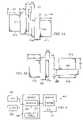
- FIGS. 1A and 1BAn example of a double exposure phase shift method is illustrated in FIGS. 1A and 1B .
- FIG. 1Ashows a layout of the mask features including the binary gate mask and phase shift features needed for each phase shift printed transistor.
- FIG. 1Ashows a layout 100 of the overlay of a binary photomask and an altPSM over active areas 102 .
- the binary photomaskincludes a series of binary gate layouts 112 .
- the altPSMincludes the phase shifters (also called shifters) 122 a and 122 b, where phase shifters 122 a have a 0° phase shift and phase shifters 122 b have a 180° phase shift.
- a photoresistis applied to a wafer and the wafer is exposed to both masks in succession followed by photoresist development.
- the final transistors 132 and 134 formed using the two masks shown in FIG. 1Aare shown in FIG. 1B .
- At least one phase shifteris placed on a side of a feature that is to be reduced in size.
- shifters 122 a and 122 bare placed on both sides of gate layouts 112 .
- the features that are to be reduced in sizeare often placed next to other features, which themselves are to be reduced in size. As such, there is a limited amount of space in which to place the shifters.
- shifter 122 bis placed in the space D 1 .
- the shifter 122 bhas a width D 2 sufficiently less than the size of the space D 1 and can be placed into the allotted space.
- gate layout 212 ais spaced at the same distance from gate layout 212 b as gate layout 212 c is spaced from gate layout 212 d and gate layout 212 b is spaced a distance D 2 from gate layout 212 C, where D 1 is different than D 2 .
- a space having width D 3is allotted for shifters on the sides of gate layout 212 a and gate layout 212 b that face each other and the space D 3 is also allotted for shifters on the sides of gate layout 212 c and gate layout 212 d that face each other.
- the space having width D 4is allotted for shifters in the space having distance D 2 on the sides of gate layout 212 b and gate layout 212 c that face each other.
- the space D 1is different from the space D 2 because gate layout 212 b is separated from gate layout 212 c by a different amount than gate layout 212 a is separated from gate layout 212 b.
- conventional methodsare only capable of using the same shifter width, shown here as width D 5 , for all situations.
- shifters 222 a and 222 b that have the same width D 5are used in each space D 4 and D 4 .
- gate layouts 212 a and 212 b and gate layouts 212 c and 212 dare spaced close together, the shifters having width D 5 fill almost all of the allowable space D 3 , which causes the gate features to print incorrectly.
- gate layout 212 bis space far from gate layout 212 c.
- the shifters having width D 5do not provide an appropriate amount of coverage, which also causes the gate features to print incorrectly.
- FIG. 2Bdepicts another example of a case where merged shifters are unacceptable.
- gate layout 212is perpendicular to gate layout 216 and the shifters 222 a, 222 b, 226 a, and 226 b, which are the same standard size, overlap. In this case, the merged shifters cause the gate features to print incorrectly.
- the present inventionsolves these and other problems of the prior art to provide a method that can design layouts having maximum and/or variable shifter widths to allow altPSM implementation for dense or existing layouts.
- the methodcan comprise determining a maximum width of a shifter, wherein the maximum width corresponds to a width of a shifter for a first set of features and determining whether the shifter having the maximum width can be placed in a shifter space for a second set of features.
- the methodcan also comprise incrementally decreasing the width of the shifter to be placed into the shifter space for the second set of features when the shifter having the maximum width cannot be placed in the shifter space for a feature in the second set of features until an acceptable shifter width can be determined or until the shifter width is reduced to a predetermined minimum shifter width.
- a method of designing a lithography maskcan comprise determining a first shifter width based on a shifter space associated with a critical dimension feature and attempting to place a shifter having the first shifter width in a shifter space other than the shifter space associated with the critical dimension feature.
- the methodcan also comprise reducing a width of a shifter having the first shifter width when the width of the shifter having the first shifter width is larger than an allowed shifter width until the width of the shifter is allowed or until the width of the shifter is less than a minimum shifter width.
- a computer readable mediumcomprising program code that configures a processor to perform a method of correcting a lithography mask.
- the computer readable mediumcan comprise program code for determining a maximum width of a shifter, wherein the maximum width corresponds to a width of a shifter for a first set of features and program code for determining whether the shifter having the maximum width can be placed in a shifter space for a second set of features.
- the computer readable mediumcan also comprise program code for incrementally decreasing the width of the shifter to be placed into the shifter space for the second set of features when the shifter having the maximum width cannot be placed in the shifter space for a feature in the second set of features until an acceptable shifter width can be determined or until the shifter width is reduced to a predetermined minimum shifter width.
- FIG. 1Ais a diagram illustrating a layout of an overlay of a binary photomask and an alternating phase shift photomask.
- FIG. 1Bis a diagram illustrating a the final structures formed using the layout shown in FIG. 1A .
- FIG. 2Ais a diagram illustrating a conventional layout of an overlay of a binary photomask and an alternating phase shift photomask.
- FIG. 2Bis another diagram illustrating a conventional layout of an overlay of a binary photomask and an alternating phase shift photomask.
- FIG. 2Cis another diagram illustrating a conventional layout of an overlay of a binary photomask and an alternating phase shift photomask.
- FIG. 3is a flowchart illustrating one embodiment of a method that can design layouts having maximum and/or variable shifter widths to allow altPSM implementation for dense or existing layouts.
- FIG. 4is a diagram illustrating a layout of an overlay of a photomask and an alternating phase shift photomask in accordance with the present teachings.
- FIG. 5Ais a diagram illustrating a layout that cannot be merged.
- FIG. 5Bis a diagram illustrating another layout that cannot be merged.
- FIG. 6illustrates a system for designing and correcting a photomask according to the present teachings.
- FIGS. 3 to 6 of the drawingslike numerals being used for like and corresponding parts of the various drawings.
- FIG. 3shows a flowchart 300 illustrating various embodiments of a method for placing shifters on a layout.
- shiftersis used interchangeably with the term “phase shifter” and refers to the regions of the photomasks designed to produce destructive interference and produce a high-contrast pattern.
- the methoddetermines a maximum size that a shifter can have and still be acceptable for use in the shifter space associated with a critical dimension (CD) feature, such as minimum-contact-pitch.
- the sizecan be, for example, width and/or length.
- the maximum target shifter widthis determined so as to minimize sensitivity of the printed feature to other imaging parameters; e.g., scanner defocus and flare and trim-to-phase misalignment.
- this widthis typically 180-250 nm.
- the methodattempts to place a shifter having the maximum width in a shifter space associated with another feature of the layout, such as an isolated line. For example, at 320 the method determines whether the maximum width shifter can fit into the shifter space without causing a problem, such as a design rule violation. If the width of the shifter is acceptable, the method places the shifter in the layout, as shown at 325 . If the width of the shifter is too large, the method reduces the width, and possibly other dimensions, to allow the shifter to fit acceptably into the allotted space, as shown at 330 .
- the methodcan attempt to automatically place and incrementally a smaller shifter into the allotted space.
- the shifter widthis reduced by 10 nm per iteration.
- the methodanalyzes whether the incrementally smaller shifter width is smaller than a minimum width that can be tolerated by the lithography system. This minimum width can be predetermined by a user or by the process tools. For 193-nm exposure, this width is typically 110-150 nm. If the incrementally smaller shifter width is not smaller than the minimum width, the method can go back to step 320 to again determine whether the maximum width shifter can fit into the shifter space without causing a problem. If it is determined that the shifter is smaller than the minimum width, the shifter space and/or the shifter is flagged for attention, as shown at 340 . For example, the method can mark flag the shifter space and/or shifter as being a design rule violation.
- FIG. 4illustrates a layout 400 of the overlay of a binary photomask and an altPSM over active areas 402 .
- the binary photomaskincludes a series of binary gate layouts 412 a - c and 414 a - b.
- the altPSMincludes the shifters 422 a, 422 b, 422 c, 424 a, 424 b, and 424 c, where phase shifters 422 a and 424 a have a 0° phase shift and phase shifters 422 b, 422 c, and 424 b have a 180° phase shift.
- a photoresistis applied to a wafer and the wafer is exposed to both masks in succession followed by photoresist development.
- gate layouts 412 a - care separated from each other at the same spacing, D 9 , and gate layout 414 a is spaced from gate layout 412 c by a space D 10 , and gate layout 414 a is spaced from gate layout 414 b by a space D 11 , where D 11 is different than D 10 and D 9 , and D 10 is different than D 9 .
- shifters having different sizescan be positioned in the allotted spaces.
- shifters having a width of D 12can be used in the allocated space D 13 between the gate layouts 412 a and 412 b and between the gate layouts 412 b and 412 c. These shifters can be the same size, D 12 .
- a shifter having a width of D 14can be used in the allocated space having width D 15 and a shifter of width D 16 can be used in the allocated space having D 17 between the gate layouts 412 c and 414 a.
- a shifter having a width of D 19can be used in the space having width D 20 between the gate layouts 414 a and 414 b.
- the method described hereincan vary the size of the shifters to provide improved processing.
- FIGS. 5A and 5Billustrate instances where layouts 500 and 550 , respectively, cannot be merged.
- FIG. 5Ashows gate layouts 512 and 514 .
- the altPSMincludes the shifters 522 a, 522 b, 524 a, and 524 b, where phase shifters 522 a and 524 a have a 0° phase shift and phase shifters 522 b and 524 b have a 180° phase shift.
- FIG. 5Bshows gate layouts 562 and 564 .
- the altPSMincludes the shifters 572 a, 572 b, 574 a, and 574 b, where phase shifters 572 a and 574 a have a 0° phase shift and phase shifters 572 b and 574 b have a 180° phase shift.
- a photoresistis applied to a wafer and the wafer is exposed to both masks in succession followed by photoresist development.
- the gate layouts 512is shown parallel to gate layout 514 and gate layout 562 is perpendicular to gate layout 514 .
- shifters having different sizescan be positioned in the allotted spaces.
- shifter 522 acan have a width of D 21 and can be positioned in a space having a width D 22 and shifter 524 b can have a width of D 23 and can be positioned in a space having a width D 25 .
- shifter 522 bcan have a width of D 31 and can be positioned in a spacing having a width D 32 and shifter 524 a can have a width of D 33 and can be positioned in a spacing having a width D 35 .
- shifter 572 acan have a width of D 81 and can be positioned in a space having a width D 82 and shifter 574 b can have a width of D 83 and can be positioned in a space having a width D 85 .
- shifter 572 bcan have a width of D 91 and can be positioned in a spacing having a width D 92 and shifter 574 a can have a width of D 93 and can be positioned in a spacing having a width D 95 .
- the shifterscan be positioned in the allotted spaces without forming merged shifters. Further, the shifters are optimized to the space and phase shift required to produce accurate features on a substrate.
- FIG. 6illustrates a system 600 that can be used to designing and correcting a mask pattern, such as a pattern on a phase photomask and/or a trim photomask described herein.
- System 600includes an input device 620 and an output device 630 coupled to a computer 640 , which is in turn coupled to a database 650 .
- Input device 620may comprise, for example, a keyboard, a mouse, or any other device suitable for transmitting data to computer 640 .
- Output device 630may comprise, for example, a display, a printer, or any other device suitable for outputting data received from computer 640 .
- Computer 640may comprise a personal computer, workstation, network computer, wireless computer, or one or more microprocessors within these or other devices, or any other suitable processing device.
- Computer 640may include a processor 660 and a correction module 670 .
- Processor 660controls the flow of data between input device 620 , output device 630 , database 650 , and correction module 670 .
- Correction module 670may receive descriptions of a contour and an uncorrected pattern and can compute a corrected pattern that maybe used to define the contour.
- Database 650may comprise any suitable system for storing data.
- Database 650may store records 680 that include data associated with the layouts.
- a record 680may be associated with a segment of the layout.
- the methods and systems described hereinmay also be used to correct patterns of other layers of integrated circuits.
- the interconnect parts of a metal patternmay be divided into base and relational segments for improved critical dimension correction, leaving the corners and contact/via pads to be corrected as traditional placement-correction segments.
Landscapes
- Physics & Mathematics (AREA)
- General Physics & Mathematics (AREA)
- Preparing Plates And Mask In Photomechanical Process (AREA)
Abstract
Description
- This invention relates generally to the field of integrated circuits and more specifically to a method and system for using alternating phase-shift implementation in lithographic processes.
- Conventional optical projection lithography has been the standard silicon patterning technology for the past 20 years. It is an economical process due to its inherently high throughput, thereby providing a desirable low cost per part or die produced. A considerable infrastructure (including steppers, photomasks, resists, metrology, etc) has been built up around this technology.
- In this process, a mask, or “reticle”, includes a semiconductor circuit layout pattern typically formed of opaque chrome, on a transparent glass (typically SiO2) substrate. A stepper includes a light source and optics/lenses that project light coming through the reticle and images the circuit pattern, typically with a 4× to 5× reduction factor, on a photo-resist film formed on a silicon wafer. The term “chrome” refers to an opaque masking material that is typically but not always comprised of chrome. The transmission of the opaque material may also vary such as in the case of an attenuating phase shift mask.
- As the semiconductor industry continues to evolve, feature sizes of the pattern are driven to smaller resolution. To meet this demand, Resolution-Enhanced optical lithography Technologies (“RET”) have become popular as techniques for providing patterns with sub-wavelength resolution. These methods include off-axis illumination (“OAI”), optical proximity correction (“OPC”), and phase-shift masks (“PSMs”). Such resolution-enhanced optical lithography methods are especially useful for generating physical devices on a wafer that require small size and tight design tolerance. Examples of such physical devices are the gate length of a transistor or the dimensions of contact cuts formed in inter-layer dielectrics.
- One of the most common commercial implementations of phase shift mask technology is the double exposure method. A first mask, often called a binary mask, contains most of the features at the gate level. The binary mask can be printed using standard lithography techniques. A second mask, often called an alternating phase-shift mask (altPSM) includes the critical, or small sized features at the gate level.
- An example of a double exposure phase shift method is illustrated in
FIGS. 1A and 1B .FIG. 1A shows a layout of the mask features including the binary gate mask and phase shift features needed for each phase shift printed transistor.FIG. 1A shows alayout 100 of the overlay of a binary photomask and an altPSM overactive areas 102. The binary photomask includes a series ofbinary gate layouts 112. The altPSM includes the phase shifters (also called shifters)122aand122b,wherephase shifters 122ahave a 0° phase shift andphase shifters 122bhave a 180° phase shift. In use, a photoresist is applied to a wafer and the wafer is exposed to both masks in succession followed by photoresist development. Thefinal transistors FIG. 1A are shown inFIG. 1B . - At least one phase shifter is placed on a side of a feature that is to be reduced in size. In
FIG. 1A ,shifters gate layouts 112. The features that are to be reduced in size are often placed next to other features, which themselves are to be reduced in size. As such, there is a limited amount of space in which to place the shifters. InFIG. 1A , for example,shifter 122bis placed in the space D1. In this case, theshifter 122bhas a width D2 sufficiently less than the size of the space D1 and can be placed into the allotted space. - Problems arise, however, when designing an altPSM used to produce regions of a layouts having dense features and isolated features, such as arrays of transistors in random logic designs and where features are perpendicular to each other. For example, the width of phase shifters for isolated lines must be optimized to give maximum process margin. The optimal solution often produces shifter widths that are large in comparison to the spaces in the layout in which they must fit. Conventional layouts, however, use the same size default shifter for each feature to be reduced in size. The conventional methods are incapable of varying the shifter size so the shifter cannot be optimized to fit in the allotted space. As a result, problems arise, some of which are illustrated in
FIGS. 2A-2C . - For example, in
FIG. 2A gate layout 212ais spaced at the same distance fromgate layout 212basgate layout 212cis spaced fromgate layout 212dandgate layout 212bis spaced a distance D2 from gate layout212C, where D1 is different than D2. A space having width D3 is allotted for shifters on the sides ofgate layout 212aandgate layout 212bthat face each other and the space D3 is also allotted for shifters on the sides ofgate layout 212candgate layout 212dthat face each other. The space having width D4 is allotted for shifters in the space having distance D2 on the sides ofgate layout 212bandgate layout 212cthat face each other. The space D1 is different from the space D2 becausegate layout 212bis separated fromgate layout 212cby a different amount thangate layout 212ais separated fromgate layout 212b.As mentioned, conventional methods are only capable of using the same shifter width, shown here as width D5, for all situations. Thus,shifters gate layouts gate layouts gate layout 212bis space far fromgate layout 212c.The shifters having width D5 do not provide an appropriate amount of coverage, which also causes the gate features to print incorrectly. - As shown in
FIG. 2B , trying to fit the shifters of width D6 into a space of width D7 causes the shifters to merge into a single shifter. While in some cases merged shifters may be acceptable, in many cases, merged shifters cannot be used as they incorrectly trim the printed features or fail to reproduce an intended feature on a substrate.FIG. 2C depicts another example of a case where merged shifters are unacceptable. InFIG. 2C ,gate layout 212 is perpendicular togate layout 216 and theshifters - Accordingly, the present invention solves these and other problems of the prior art to provide a method that can design layouts having maximum and/or variable shifter widths to allow altPSM implementation for dense or existing layouts.
- In accordance with an embodiment of the invention, there is a method of designing a lithography mask. The method can comprise determining a maximum width of a shifter, wherein the maximum width corresponds to a width of a shifter for a first set of features and determining whether the shifter having the maximum width can be placed in a shifter space for a second set of features. The method can also comprise incrementally decreasing the width of the shifter to be placed into the shifter space for the second set of features when the shifter having the maximum width cannot be placed in the shifter space for a feature in the second set of features until an acceptable shifter width can be determined or until the shifter width is reduced to a predetermined minimum shifter width.
- In accordance with another embodiment of the invention, there is a method of designing a lithography mask. The method can comprise determining a first shifter width based on a shifter space associated with a critical dimension feature and attempting to place a shifter having the first shifter width in a shifter space other than the shifter space associated with the critical dimension feature. The method can also comprise reducing a width of a shifter having the first shifter width when the width of the shifter having the first shifter width is larger than an allowed shifter width until the width of the shifter is allowed or until the width of the shifter is less than a minimum shifter width.
- In accordance with another embodiment of the invention, there is a computer readable medium comprising program code that configures a processor to perform a method of correcting a lithography mask. The computer readable medium can comprise program code for determining a maximum width of a shifter, wherein the maximum width corresponds to a width of a shifter for a first set of features and program code for determining whether the shifter having the maximum width can be placed in a shifter space for a second set of features. The computer readable medium can also comprise program code for incrementally decreasing the width of the shifter to be placed into the shifter space for the second set of features when the shifter having the maximum width cannot be placed in the shifter space for a feature in the second set of features until an acceptable shifter width can be determined or until the shifter width is reduced to a predetermined minimum shifter width.
- Additional advantages of the embodiments will be set forth in part in the description which follows, and in part will be obvious from the description, or may be learned by practice of the invention. The advantages will be realized and attained by means of the elements and combinations particularly pointed out in the appended claims.
- It is to be understood that both the foregoing general description and the following detailed description are exemplary and explanatory only and are not restrictive of the invention, as claimed.
- The accompanying drawings, which are incorporated in and constitute a part of this specification, illustrate embodiments of the invention and together with the description, serve to explain the principles of the invention.
FIG. 1A is a diagram illustrating a layout of an overlay of a binary photomask and an alternating phase shift photomask.FIG. 1B . is a diagram illustrating a the final structures formed using the layout shown inFIG. 1A .FIG. 2A is a diagram illustrating a conventional layout of an overlay of a binary photomask and an alternating phase shift photomask.FIG. 2B is another diagram illustrating a conventional layout of an overlay of a binary photomask and an alternating phase shift photomask.FIG. 2C is another diagram illustrating a conventional layout of an overlay of a binary photomask and an alternating phase shift photomask.FIG. 3 is a flowchart illustrating one embodiment of a method that can design layouts having maximum and/or variable shifter widths to allow altPSM implementation for dense or existing layouts.FIG. 4 is a diagram illustrating a layout of an overlay of a photomask and an alternating phase shift photomask in accordance with the present teachings.FIG. 5A is a diagram illustrating a layout that cannot be merged.FIG. 5B is a diagram illustrating another layout that cannot be merged.FIG. 6 illustrates a system for designing and correcting a photomask according to the present teachings.- Reference will now be made in detail to the present embodiments, examples of which are illustrated in the accompanying drawings. Wherever possible, the same reference numbers will be used throughout the drawings to refer to the same or like parts.
- Notwithstanding that the numerical ranges and parameters setting forth the broad scope of the invention are approximations, the numerical values set forth in the specific examples are reported as precisely as possible. Any numerical value, however, inherently contains certain errors necessarily resulting from the standard deviation found in their respective testing measurements. Moreover, all ranges disclosed herein are to be understood to encompass any and all sub-ranges subsumed therein. For example, a range of “less than 10” can include any and all sub-ranges between (and including) the minimum value of zero and the maximum value of 10, that is, any and all sub-ranges having a minimum value of equal to or greater than zero and a maximum value of equal to or less than 10, e.g., 1 to 5.
- Embodiments of the present invention and its advantages are best understood by referring to
FIGS. 3 to 6 of the drawings, like numerals being used for like and corresponding parts of the various drawings. FIG. 3 shows aflowchart 300 illustrating various embodiments of a method for placing shifters on a layout. As used herein, the term “shifters” is used interchangeably with the term “phase shifter” and refers to the regions of the photomasks designed to produce destructive interference and produce a high-contrast pattern. At310, the method determines a maximum size that a shifter can have and still be acceptable for use in the shifter space associated with a critical dimension (CD) feature, such as minimum-contact-pitch. The size can be, for example, width and/or length. The maximum target shifter width is determined so as to minimize sensitivity of the printed feature to other imaging parameters; e.g., scanner defocus and flare and trim-to-phase misalignment. For a 193-nm exposure tool, this width is typically 180-250 nm. At315, the method attempts to place a shifter having the maximum width in a shifter space associated with another feature of the layout, such as an isolated line. For example, at320 the method determines whether the maximum width shifter can fit into the shifter space without causing a problem, such as a design rule violation. If the width of the shifter is acceptable, the method places the shifter in the layout, as shown at325. If the width of the shifter is too large, the method reduces the width, and possibly other dimensions, to allow the shifter to fit acceptably into the allotted space, as shown at330. According to various embodiments, the method can attempt to automatically place and incrementally a smaller shifter into the allotted space. For example, in a typical embodiment, the shifter width is reduced by10 nm per iteration. At335, the method analyzes whether the incrementally smaller shifter width is smaller than a minimum width that can be tolerated by the lithography system. This minimum width can be predetermined by a user or by the process tools. For 193-nm exposure, this width is typically 110-150 nm. If the incrementally smaller shifter width is not smaller than the minimum width, the method can go back to step320 to again determine whether the maximum width shifter can fit into the shifter space without causing a problem. If it is determined that the shifter is smaller than the minimum width, the shifter space and/or the shifter is flagged for attention, as shown at340. For example, the method can mark flag the shifter space and/or shifter as being a design rule violation.FIG. 4 illustrates alayout 400 of the overlay of a binary photomask and an altPSM overactive areas 402. The binary photomask includes a series of binary gate layouts412a-cand414a-b.The altPSM includes theshifters phase shifters phase shifters gate layout 414ais spaced fromgate layout 412cby a space D10, andgate layout 414ais spaced fromgate layout 414bby a space D11, where D11 is different than D10 and D9, and D10 is different than D9.- Using the teachings described herein, shifters having different sizes can be positioned in the allotted spaces. For example, shifters having a width of D12 can be used in the allocated space D13 between the
gate layouts gate layouts gate layouts gate layouts FIGS. 5A and 5B illustrate instances where layouts500 and550, respectively, cannot be merged. For example,FIG. 5A showsgate layouts shifters phase shifters phase shifters FIG. 5B showsgate layouts shifters phase shifters phase shifters FIG. 5A , thegate layouts 512 is shown parallel togate layout 514 andgate layout 562 is perpendicular togate layout 514.- As described, using the teachings described herein, shifters having different sizes can be positioned in the allotted spaces. For example, in
FIG. 5A shifter 522acan have a width of D21 and can be positioned in a space having a width D22 andshifter 524bcan have a width of D23 and can be positioned in a space having a width D25. Similarly,shifter 522bcan have a width of D31 and can be positioned in a spacing having a width D32 andshifter 524acan have a width of D33 and can be positioned in a spacing having a width D35. - In
FIG. 5B ,shifter 572acan have a width of D81 and can be positioned in a space having a width D82 andshifter 574bcan have a width of D83 and can be positioned in a space having a width D85. Similarly,shifter 572bcan have a width of D91 and can be positioned in a spacing having a width D92 andshifter 574acan have a width of D93 and can be positioned in a spacing having a width D95. - Because the present teachings permit shifters of various sizes, the shifters can be positioned in the allotted spaces without forming merged shifters. Further, the shifters are optimized to the space and phase shift required to produce accurate features on a substrate.
FIG. 6 illustrates asystem 600 that can be used to designing and correcting a mask pattern, such as a pattern on a phase photomask and/or a trim photomask described herein.System 600 includes aninput device 620 and anoutput device 630 coupled to acomputer 640, which is in turn coupled to adatabase 650.Input device 620 may comprise, for example, a keyboard, a mouse, or any other device suitable for transmitting data tocomputer 640.Output device 630 may comprise, for example, a display, a printer, or any other device suitable for outputting data received fromcomputer 640.Computer 640 may comprise a personal computer, workstation, network computer, wireless computer, or one or more microprocessors within these or other devices, or any other suitable processing device.Computer 640 may include aprocessor 660 and acorrection module 670.Processor 660 controls the flow of data betweeninput device 620,output device 630,database 650, andcorrection module 670.Correction module 670 may receive descriptions of a contour and an uncorrected pattern and can compute a corrected pattern that maybe used to define the contour.Database 650 may comprise any suitable system for storing data.Database 650 may storerecords 680 that include data associated with the layouts. Arecord 680 may be associated with a segment of the layout.- While the examples given have been with respect to patterning transistor gates over diffusion regions, the methods and systems described herein may also be used to correct patterns of other layers of integrated circuits. For example, the interconnect parts of a metal pattern may be divided into base and relational segments for improved critical dimension correction, leaving the corners and contact/via pads to be corrected as traditional placement-correction segments.
- While the invention has been illustrated with respect to one or more implementations, alterations and/or modifications can be made to the illustrated examples without departing from the spirit and scope of the appended claims. In addition, while a particular feature of the invention may have been disclosed with respect to only one of several implementations, such feature may be combined with one or more other features of the other implementations as may be desired and advantageous for any given or particular function. Furthermore, to the extent that the terms “including”, “includes”, “having”, “has”, “with”, or variants thereof are used in either the detailed description and the claims, such terms are intended to be inclusive in a manner similar to the term “comprising.”
- Other embodiments of the invention will be apparent to those skilled in the art from consideration of the specification and practice of the invention disclosed herein. It is intended that the specification and examples be considered as exemplary only, with a true scope and spirit of the invention being indicated by the following claims.
Claims (21)
Priority Applications (1)
| Application Number | Priority Date | Filing Date | Title |
|---|---|---|---|
| US11/565,215US7774739B2 (en) | 2006-11-30 | 2006-11-30 | Methods for adjusting shifter width of an alternating phase shifter having variable width |
Applications Claiming Priority (1)
| Application Number | Priority Date | Filing Date | Title |
|---|---|---|---|
| US11/565,215US7774739B2 (en) | 2006-11-30 | 2006-11-30 | Methods for adjusting shifter width of an alternating phase shifter having variable width |
Publications (2)
| Publication Number | Publication Date |
|---|---|
| US20080134128A1true US20080134128A1 (en) | 2008-06-05 |
| US7774739B2 US7774739B2 (en) | 2010-08-10 |
Family
ID=39477364
Family Applications (1)
| Application Number | Title | Priority Date | Filing Date |
|---|---|---|---|
| US11/565,215Active2027-03-20US7774739B2 (en) | 2006-11-30 | 2006-11-30 | Methods for adjusting shifter width of an alternating phase shifter having variable width |
Country Status (1)
| Country | Link |
|---|---|
| US (1) | US7774739B2 (en) |
Cited By (26)
| Publication number | Priority date | Publication date | Assignee | Title |
|---|---|---|---|---|
| US20080222587A1 (en)* | 2007-03-05 | 2008-09-11 | Tela Innovations, Inc. | Integrated Circuit Cell Library for Multiple Patterning |
| US20100187622A1 (en)* | 2008-03-13 | 2010-07-29 | Tela Innovations, Inc. | Linear Gate Level Cross-Coupled Transistor Device with Complimentary Pairs of Cross-Coupled Transistors Defined by Physically Separate Gate Electrodes within Gate Electrode Level |
| US8225239B2 (en) | 2006-03-09 | 2012-07-17 | Tela Innovations, Inc. | Methods for defining and utilizing sub-resolution features in linear topology |
| US8225261B2 (en) | 2006-03-09 | 2012-07-17 | Tela Innovations, Inc. | Methods for defining contact grid in dynamic array architecture |
| US8245180B2 (en) | 2006-03-09 | 2012-08-14 | Tela Innovations, Inc. | Methods for defining and using co-optimized nanopatterns for integrated circuit design and apparatus implementing same |
| US8247846B2 (en) | 2006-03-09 | 2012-08-21 | Tela Innovations, Inc. | Oversized contacts and vias in semiconductor chip defined by linearly constrained topology |
| US8253172B2 (en) | 2006-03-09 | 2012-08-28 | Tela Innovations, Inc. | Semiconductor device with linearly restricted gate level region including four serially connected transistors of first type and four serially connected transistors of second type separated by non-diffusion region |
| US8283701B2 (en) | 2007-08-02 | 2012-10-09 | Tela Innovations, Inc. | Semiconductor device with dynamic array sections defined and placed according to manufacturing assurance halos |
| US8286107B2 (en) | 2007-02-20 | 2012-10-09 | Tela Innovations, Inc. | Methods and systems for process compensation technique acceleration |
| US8448102B2 (en) | 2006-03-09 | 2013-05-21 | Tela Innovations, Inc. | Optimizing layout of irregular structures in regular layout context |
| US8453094B2 (en) | 2008-01-31 | 2013-05-28 | Tela Innovations, Inc. | Enforcement of semiconductor structure regularity for localized transistors and interconnect |
| US8471391B2 (en) | 2008-03-27 | 2013-06-25 | Tela Innovations, Inc. | Methods for multi-wire routing and apparatus implementing same |
| US8541879B2 (en) | 2007-12-13 | 2013-09-24 | Tela Innovations, Inc. | Super-self-aligned contacts and method for making the same |
| US8549455B2 (en) | 2007-08-02 | 2013-10-01 | Tela Innovations, Inc. | Methods for cell phasing and placement in dynamic array architecture and implementation of the same |
| US8653857B2 (en) | 2006-03-09 | 2014-02-18 | Tela Innovations, Inc. | Circuitry and layouts for XOR and XNOR logic |
| US8661392B2 (en) | 2009-10-13 | 2014-02-25 | Tela Innovations, Inc. | Methods for cell boundary encroachment and layouts implementing the Same |
| US8658542B2 (en) | 2006-03-09 | 2014-02-25 | Tela Innovations, Inc. | Coarse grid design methods and structures |
| US8680626B2 (en) | 2007-10-26 | 2014-03-25 | Tela Innovations, Inc. | Methods, structures, and designs for self-aligning local interconnects used in integrated circuits |
| US8839175B2 (en) | 2006-03-09 | 2014-09-16 | Tela Innovations, Inc. | Scalable meta-data objects |
| US8863063B2 (en) | 2009-05-06 | 2014-10-14 | Tela Innovations, Inc. | Finfet transistor circuit |
| US9035359B2 (en) | 2006-03-09 | 2015-05-19 | Tela Innovations, Inc. | Semiconductor chip including region including linear-shaped conductive structures forming gate electrodes and having electrical connection areas arranged relative to inner region between transistors of different types and associated methods |
| US9122832B2 (en) | 2008-08-01 | 2015-09-01 | Tela Innovations, Inc. | Methods for controlling microloading variation in semiconductor wafer layout and fabrication |
| US9159627B2 (en) | 2010-11-12 | 2015-10-13 | Tela Innovations, Inc. | Methods for linewidth modification and apparatus implementing the same |
| US9230910B2 (en) | 2006-03-09 | 2016-01-05 | Tela Innovations, Inc. | Oversized contacts and vias in layout defined by linearly constrained topology |
| US9563733B2 (en) | 2009-05-06 | 2017-02-07 | Tela Innovations, Inc. | Cell circuit and layout with linear finfet structures |
| US10216890B2 (en) | 2004-04-21 | 2019-02-26 | Iym Technologies Llc | Integrated circuits having in-situ constraints |
Citations (8)
| Publication number | Priority date | Publication date | Assignee | Title |
|---|---|---|---|---|
| US5862058A (en)* | 1996-05-16 | 1999-01-19 | International Business Machines Corporation | Optical proximity correction method and system |
| US20040096752A1 (en)* | 2002-11-20 | 2004-05-20 | International Business Machines Corporation | Phase-width balanced alternating phase shift mask design |
| US6757886B2 (en)* | 2001-11-13 | 2004-06-29 | International Business Machines Corporation | Alternating phase shift mask design with optimized phase shapes |
| US6813759B2 (en)* | 2002-09-09 | 2004-11-02 | Numerical Technologies, Inc. | Hybrid optical proximity correction for alternating aperture phase shifting designs |
| US7132203B2 (en)* | 2000-07-05 | 2006-11-07 | Synopsys, Inc. | Phase shift masking for complex patterns with proximity adjustments |
| US7332250B2 (en)* | 2003-06-24 | 2008-02-19 | Matsushita Electric Industrial Co., Ltd. | Photomask |
| US7399557B2 (en)* | 2003-06-05 | 2008-07-15 | Kabushiki Kaisha Toshiba | Photomask correcting method and manufacturing method of semiconductor device |
| US7459243B2 (en)* | 2003-12-19 | 2008-12-02 | Oki Electric Industry Co., Ltd. | Method of correcting mask pattern |
- 2006
- 2006-11-30USUS11/565,215patent/US7774739B2/enactiveActive
Patent Citations (8)
| Publication number | Priority date | Publication date | Assignee | Title |
|---|---|---|---|---|
| US5862058A (en)* | 1996-05-16 | 1999-01-19 | International Business Machines Corporation | Optical proximity correction method and system |
| US7132203B2 (en)* | 2000-07-05 | 2006-11-07 | Synopsys, Inc. | Phase shift masking for complex patterns with proximity adjustments |
| US6757886B2 (en)* | 2001-11-13 | 2004-06-29 | International Business Machines Corporation | Alternating phase shift mask design with optimized phase shapes |
| US6813759B2 (en)* | 2002-09-09 | 2004-11-02 | Numerical Technologies, Inc. | Hybrid optical proximity correction for alternating aperture phase shifting designs |
| US20040096752A1 (en)* | 2002-11-20 | 2004-05-20 | International Business Machines Corporation | Phase-width balanced alternating phase shift mask design |
| US7399557B2 (en)* | 2003-06-05 | 2008-07-15 | Kabushiki Kaisha Toshiba | Photomask correcting method and manufacturing method of semiconductor device |
| US7332250B2 (en)* | 2003-06-24 | 2008-02-19 | Matsushita Electric Industrial Co., Ltd. | Photomask |
| US7459243B2 (en)* | 2003-12-19 | 2008-12-02 | Oki Electric Industry Co., Ltd. | Method of correcting mask pattern |
Cited By (136)
| Publication number | Priority date | Publication date | Assignee | Title |
|---|---|---|---|---|
| US10846454B2 (en) | 2004-04-21 | 2020-11-24 | Iym Technologies Llc | Integrated circuits having in-situ constraints |
| US10860773B2 (en) | 2004-04-21 | 2020-12-08 | Iym Technologies Llc | Integrated circuits having in-situ constraints |
| US10216890B2 (en) | 2004-04-21 | 2019-02-26 | Iym Technologies Llc | Integrated circuits having in-situ constraints |
| US9905576B2 (en) | 2006-03-09 | 2018-02-27 | Tela Innovations, Inc. | Semiconductor chip including region having rectangular-shaped gate structures and first metal structures |
| US8448102B2 (en) | 2006-03-09 | 2013-05-21 | Tela Innovations, Inc. | Optimizing layout of irregular structures in regular layout context |
| US8247846B2 (en) | 2006-03-09 | 2012-08-21 | Tela Innovations, Inc. | Oversized contacts and vias in semiconductor chip defined by linearly constrained topology |
| US8253172B2 (en) | 2006-03-09 | 2012-08-28 | Tela Innovations, Inc. | Semiconductor device with linearly restricted gate level region including four serially connected transistors of first type and four serially connected transistors of second type separated by non-diffusion region |
| US8253173B2 (en) | 2006-03-09 | 2012-08-28 | Tela Innovations, Inc. | Semiconductor device with gate level including four transistors of first type and four transistors of second type separated by non-diffusion region and having at least two gate contacts positioned outside separating non-diffusion region |
| US8258552B2 (en) | 2006-03-09 | 2012-09-04 | Tela Innovations, Inc. | Semiconductor device including at least six transistor forming linear shapes with at least two transistor forming linear shapes having offset ends |
| US8258547B2 (en) | 2006-03-09 | 2012-09-04 | Tela Innovations, Inc. | Semiconductor device with linearly restricted gate level region including two transistors of first type and two transistors of second type with offset gate contacts |
| US8258548B2 (en) | 2006-03-09 | 2012-09-04 | Tela Innovations, Inc. | Semiconductor device with gate level including four transistors of first type and four transistors of second type separated by non-diffusion region with restricted gate contact placement over separating non-diffusion region |
| US8921897B2 (en) | 2006-03-09 | 2014-12-30 | Tela Innovations, Inc. | Integrated circuit with gate electrode conductive structures having offset ends |
| US8258549B2 (en) | 2006-03-09 | 2012-09-04 | Tela Innovations, Inc. | Semiconductor device including two transistors of first type having gates formed by conductors of different length respectively aligned with two transistors of second type having gates formed by conductors of different length |
| US8225261B2 (en) | 2006-03-09 | 2012-07-17 | Tela Innovations, Inc. | Methods for defining contact grid in dynamic array architecture |
| US8258551B2 (en) | 2006-03-09 | 2012-09-04 | Tela Innovations, Inc. | Semiconductor device with gate level including transistors of first type and transistors of second type with corresponding gate contact placement restriction |
| US8264009B2 (en) | 2006-03-09 | 2012-09-11 | Tela Innovations, Inc. | Semiconductor device with linearly restricted gate level region including four transistors of first type and four transistors of second type with gate defining shapes of different length |
| US8921896B2 (en) | 2006-03-09 | 2014-12-30 | Tela Innovations, Inc. | Integrated circuit including linear gate electrode structures having different extension distances beyond contact |
| US8264008B2 (en) | 2006-03-09 | 2012-09-11 | Tela Innovations, Inc. | Semiconductor device including transistor forming linear shapes including gate portions and extending portions of different size |
| US8946781B2 (en) | 2006-03-09 | 2015-02-03 | Tela Innovations, Inc. | Integrated circuit including gate electrode conductive structures with different extension distances beyond contact |
| US8264007B2 (en) | 2006-03-09 | 2012-09-11 | Tela Innovations, Inc. | Semiconductor device including at least six transistor forming linear shapes including at least two different gate contact connection distances |
| US10230377B2 (en) | 2006-03-09 | 2019-03-12 | Tela Innovations, Inc. | Circuitry and layouts for XOR and XNOR logic |
| US8952425B2 (en) | 2006-03-09 | 2015-02-10 | Tela Innovations, Inc. | Integrated circuit including at least four linear-shaped conductive structures having extending portions of different length |
| US8245180B2 (en) | 2006-03-09 | 2012-08-14 | Tela Innovations, Inc. | Methods for defining and using co-optimized nanopatterns for integrated circuit design and apparatus implementing same |
| US9009641B2 (en) | 2006-03-09 | 2015-04-14 | Tela Innovations, Inc. | Circuits with linear finfet structures |
| US10217763B2 (en) | 2006-03-09 | 2019-02-26 | Tela Innovations, Inc. | Semiconductor chip having region including gate electrode features of rectangular shape on gate horizontal grid and first-metal structures of rectangular shape on at least eight first-metal gridlines of first-metal vertical grid |
| US8436400B2 (en) | 2006-03-09 | 2013-05-07 | Tela Innovations, Inc. | Semiconductor device with gate level including gate electrode conductors for transistors of first type and transistors of second type with some gate electrode conductors of different length |
| US9589091B2 (en) | 2006-03-09 | 2017-03-07 | Tela Innovations, Inc. | Scalable meta-data objects |
| US9035359B2 (en) | 2006-03-09 | 2015-05-19 | Tela Innovations, Inc. | Semiconductor chip including region including linear-shaped conductive structures forming gate electrodes and having electrical connection areas arranged relative to inner region between transistors of different types and associated methods |
| US9230910B2 (en) | 2006-03-09 | 2016-01-05 | Tela Innovations, Inc. | Oversized contacts and vias in layout defined by linearly constrained topology |
| US8839175B2 (en) | 2006-03-09 | 2014-09-16 | Tela Innovations, Inc. | Scalable meta-data objects |
| US8823062B2 (en) | 2006-03-09 | 2014-09-02 | Tela Innovations, Inc. | Integrated circuit with offset line end spacings in linear gate electrode level |
| US10186523B2 (en) | 2006-03-09 | 2019-01-22 | Tela Innovations, Inc. | Semiconductor chip having region including gate electrode features formed in part from rectangular layout shapes on gate horizontal grid and first-metal structures formed in part from rectangular layout shapes on at least eight first-metal gridlines of first-metal vertical grid |
| US10141335B2 (en) | 2006-03-09 | 2018-11-27 | Tela Innovations, Inc. | Semiconductor CIP including region having rectangular-shaped gate structures and first metal structures |
| US10141334B2 (en) | 2006-03-09 | 2018-11-27 | Tela Innovations, Inc. | Semiconductor chip including region having rectangular-shaped gate structures and first-metal structures |
| US9240413B2 (en) | 2006-03-09 | 2016-01-19 | Tela Innovations, Inc. | Methods, structures, and designs for self-aligning local interconnects used in integrated circuits |
| US9917056B2 (en) | 2006-03-09 | 2018-03-13 | Tela Innovations, Inc. | Coarse grid design methods and structures |
| US9336344B2 (en) | 2006-03-09 | 2016-05-10 | Tela Innovations, Inc. | Coarse grid design methods and structures |
| US8258550B2 (en) | 2006-03-09 | 2012-09-04 | Tela Innovations, Inc. | Semiconductor device including at least six transistor forming linear shapes including at least two transistor forming linear shapes having different extension distances beyond gate contact |
| US9754878B2 (en) | 2006-03-09 | 2017-09-05 | Tela Innovations, Inc. | Semiconductor chip including a chip level based on a layout that includes both regular and irregular wires |
| US8225239B2 (en) | 2006-03-09 | 2012-07-17 | Tela Innovations, Inc. | Methods for defining and utilizing sub-resolution features in linear topology |
| US9859277B2 (en) | 2006-03-09 | 2018-01-02 | Tela Innovations, Inc. | Methods, structures, and designs for self-aligning local interconnects used in integrated circuits |
| US8653857B2 (en) | 2006-03-09 | 2014-02-18 | Tela Innovations, Inc. | Circuitry and layouts for XOR and XNOR logic |
| US9741719B2 (en) | 2006-03-09 | 2017-08-22 | Tela Innovations, Inc. | Methods, structures, and designs for self-aligning local interconnects used in integrated circuits |
| US8658542B2 (en) | 2006-03-09 | 2014-02-25 | Tela Innovations, Inc. | Coarse grid design methods and structures |
| US9425272B2 (en) | 2006-03-09 | 2016-08-23 | Tela Innovations, Inc. | Semiconductor chip including integrated circuit including four transistors of first transistor type and four transistors of second transistor type with electrical connections between various transistors and methods for manufacturing the same |
| US9711495B2 (en) | 2006-03-09 | 2017-07-18 | Tela Innovations, Inc. | Oversized contacts and vias in layout defined by linearly constrained topology |
| US9673825B2 (en) | 2006-03-09 | 2017-06-06 | Tela Innovations, Inc. | Circuitry and layouts for XOR and XNOR logic |
| US9425145B2 (en) | 2006-03-09 | 2016-08-23 | Tela Innovations, Inc. | Oversized contacts and vias in layout defined by linearly constrained topology |
| US9425273B2 (en) | 2006-03-09 | 2016-08-23 | Tela Innovations, Inc. | Semiconductor chip including integrated circuit including at least five gate level conductive structures having particular spatial and electrical relationship and method for manufacturing the same |
| US9443947B2 (en) | 2006-03-09 | 2016-09-13 | Tela Innovations, Inc. | Semiconductor chip including region having integrated circuit transistor gate electrodes formed by various conductive structures of specified shape and position and method for manufacturing the same |
| US8286107B2 (en) | 2007-02-20 | 2012-10-09 | Tela Innovations, Inc. | Methods and systems for process compensation technique acceleration |
| US8667443B2 (en)* | 2007-03-05 | 2014-03-04 | Tela Innovations, Inc. | Integrated circuit cell library for multiple patterning |
| US9633987B2 (en) | 2007-03-05 | 2017-04-25 | Tela Innovations, Inc. | Integrated circuit cell library for multiple patterning |
| US20080222587A1 (en)* | 2007-03-05 | 2008-09-11 | Tela Innovations, Inc. | Integrated Circuit Cell Library for Multiple Patterning |
| US10074640B2 (en) | 2007-03-05 | 2018-09-11 | Tela Innovations, Inc. | Integrated circuit cell library for multiple patterning |
| US8966424B2 (en) | 2007-03-07 | 2015-02-24 | Tela Innovations, Inc. | Methods for cell phasing and placement in dynamic array architecture and implementation of the same |
| US9595515B2 (en) | 2007-03-07 | 2017-03-14 | Tela Innovations, Inc. | Semiconductor chip including integrated circuit defined within dynamic array section |
| US9424387B2 (en) | 2007-03-07 | 2016-08-23 | Tela Innovations, Inc. | Methods for cell phasing and placement in dynamic array architecture and implementation of the same |
| US9910950B2 (en) | 2007-03-07 | 2018-03-06 | Tela Innovations, Inc. | Methods for cell phasing and placement in dynamic array architecture and implementation of the same |
| US8356268B2 (en) | 2007-08-02 | 2013-01-15 | Tela Innovations, Inc. | Integrated circuit device including dynamic array section with gate level having linear conductive features on at least three side-by-side lines and uniform line end spacings |
| US8549455B2 (en) | 2007-08-02 | 2013-10-01 | Tela Innovations, Inc. | Methods for cell phasing and placement in dynamic array architecture and implementation of the same |
| US8759882B2 (en) | 2007-08-02 | 2014-06-24 | Tela Innovations, Inc. | Semiconductor device with dynamic array sections defined and placed according to manufacturing assurance halos |
| US8756551B2 (en) | 2007-08-02 | 2014-06-17 | Tela Innovations, Inc. | Methods for designing semiconductor device with dynamic array section |
| US8283701B2 (en) | 2007-08-02 | 2012-10-09 | Tela Innovations, Inc. | Semiconductor device with dynamic array sections defined and placed according to manufacturing assurance halos |
| US8680626B2 (en) | 2007-10-26 | 2014-03-25 | Tela Innovations, Inc. | Methods, structures, and designs for self-aligning local interconnects used in integrated circuits |
| US10734383B2 (en) | 2007-10-26 | 2020-08-04 | Tela Innovations, Inc. | Methods, structures, and designs for self-aligning local interconnects used in integrated circuits |
| US8951916B2 (en) | 2007-12-13 | 2015-02-10 | Tela Innovations, Inc. | Super-self-aligned contacts and method for making the same |
| US9281371B2 (en) | 2007-12-13 | 2016-03-08 | Tela Innovations, Inc. | Super-self-aligned contacts and method for making the same |
| US8541879B2 (en) | 2007-12-13 | 2013-09-24 | Tela Innovations, Inc. | Super-self-aligned contacts and method for making the same |
| US9818747B2 (en) | 2007-12-13 | 2017-11-14 | Tela Innovations, Inc. | Super-self-aligned contacts and method for making the same |
| US10461081B2 (en) | 2007-12-13 | 2019-10-29 | Tel Innovations, Inc. | Super-self-aligned contacts and method for making the same |
| US9202779B2 (en) | 2008-01-31 | 2015-12-01 | Tela Innovations, Inc. | Enforcement of semiconductor structure regularity for localized transistors and interconnect |
| US9530734B2 (en) | 2008-01-31 | 2016-12-27 | Tela Innovations, Inc. | Enforcement of semiconductor structure regularity for localized transistors and interconnect |
| US8701071B2 (en) | 2008-01-31 | 2014-04-15 | Tela Innovations, Inc. | Enforcement of semiconductor structure regularity for localized transistors and interconnect |
| US8453094B2 (en) | 2008-01-31 | 2013-05-28 | Tela Innovations, Inc. | Enforcement of semiconductor structure regularity for localized transistors and interconnect |
| US8847329B2 (en) | 2008-03-13 | 2014-09-30 | Tela Innovations, Inc. | Cross-coupled transistor circuit defined having diffusion regions of common node on opposing sides of same gate electrode track with at least two non-inner positioned gate contacts |
| US8680583B2 (en) | 2008-03-13 | 2014-03-25 | Tela Innovations, Inc. | Integrated circuit including cross-coupled transistors having gate electrodes formed within at least nine gate level feature layout channels |
| US8866197B2 (en) | 2008-03-13 | 2014-10-21 | Tela Innovations, Inc. | Integrated circuit including cross-coupled transistors having gate electrodes formed within gate level feature layout channels with at least two gate electrodes electrically connected to each other through another transistor forming gate level feature |
| US8853794B2 (en) | 2008-03-13 | 2014-10-07 | Tela Innovations, Inc. | Integrated circuit within semiconductor chip including cross-coupled transistor configuration |
| US8853793B2 (en) | 2008-03-13 | 2014-10-07 | Tela Innovations, Inc. | Integrated circuit including gate electrode level region including cross-coupled transistors having gate contacts located over inner portion of gate electrode level region and offset gate level feature line ends |
| US8847331B2 (en) | 2008-03-13 | 2014-09-30 | Tela Innovations, Inc. | Semiconductor chip including region having cross-coupled transistor configuration with offset electrical connection areas on gate electrode forming conductive structures and at least two different inner extension distances of gate electrode forming conductive structures |
| US9081931B2 (en) | 2008-03-13 | 2015-07-14 | Tela Innovations, Inc. | Cross-coupled transistor circuit having diffusion regions of common node on opposing sides of same gate electrode track and gate node connection through single interconnect layer |
| US9117050B2 (en) | 2008-03-13 | 2015-08-25 | Tela Innovations, Inc. | Integrated circuit including cross-coupled transistors having gate electrodes formed within gate level feature layout channels with gate contact position and offset specifications |
| US8836045B2 (en) | 2008-03-13 | 2014-09-16 | Tela Innovations, Inc. | Cross-coupled transistor circuit having diffusion regions of common node on opposing sides of same gate electrode track |
| US9208279B2 (en) | 2008-03-13 | 2015-12-08 | Tela Innovations, Inc. | Semiconductor chip including digital logic circuit including linear-shaped conductive structures having electrical connection areas located within inner region between transistors of different type and associated methods |
| US9213792B2 (en) | 2008-03-13 | 2015-12-15 | Tela Innovations, Inc. | Semiconductor chip including digital logic circuit including at least six transistors with some transistors forming cross-coupled transistor configuration and associated methods |
| US8835989B2 (en) | 2008-03-13 | 2014-09-16 | Tela Innovations, Inc. | Integrated circuit including cross-coupled transistors having gate electrodes formed within gate level feature layout channels with gate electrode placement specifications |
| US8816402B2 (en) | 2008-03-13 | 2014-08-26 | Tela Innovations, Inc. | Integrated circuit including cross-coupled transistors having gate electrodes formed within gate level feature layout channels with gate level feature layout channel including single transistor |
| US9245081B2 (en) | 2008-03-13 | 2016-01-26 | Tela Innovations, Inc. | Semiconductor chip including digital logic circuit including at least nine linear-shaped conductive structures collectively forming gate electrodes of at least six transistors with some transistors forming cross-coupled transistor configuration and associated methods |
| US8785978B2 (en) | 2008-03-13 | 2014-07-22 | Tela Innovations, Inc. | Integrated circuit including cross-coupled transistors having gate electrodes formed within gate level feature layout channels with electrical connection of cross-coupled transistors through same interconnect layer |
| US20100187622A1 (en)* | 2008-03-13 | 2010-07-29 | Tela Innovations, Inc. | Linear Gate Level Cross-Coupled Transistor Device with Complimentary Pairs of Cross-Coupled Transistors Defined by Physically Separate Gate Electrodes within Gate Electrode Level |
| US8258581B2 (en) | 2008-03-13 | 2012-09-04 | Tela Innovations, Inc. | Integrated circuit including cross-coupled transistors with two transistors of different type formed by same gate level structure and two transistors of different type formed by separate gate level structures |
| US8785979B2 (en) | 2008-03-13 | 2014-07-22 | Tela Innovations, Inc. | Integrated circuit including cross-coupled transistors having gate electrodes formed within gate level feature layout channels with two inside positioned gate contacts and two outside positioned gate contacts and electrical connection of cross-coupled transistors through same interconnect layer |
| US8264049B2 (en) | 2008-03-13 | 2012-09-11 | Tela Innovations, Inc. | Integrated circuit including cross-coupled transistors with two transistors of different type having gate electrodes formed by common gate level feature with shared diffusion regions on opposite sides of common gate level feature |
| US8772839B2 (en) | 2008-03-13 | 2014-07-08 | Tela Innovations, Inc. | Integrated circuit including cross-coupled transistors having gate electrodes formed within gate level feature layout channels with four inside positioned gate contacts having offset and aligned relationships and electrical connection of transistor gates through linear interconnect conductors in single interconnect layer |
| US10727252B2 (en) | 2008-03-13 | 2020-07-28 | Tela Innovations, Inc. | Semiconductor chip including integrated circuit having cross-coupled transistor configuration and method for manufacturing the same |
| US8742463B2 (en) | 2008-03-13 | 2014-06-03 | Tela Innovations, Inc. | Integrated circuit including cross-coupled transistors having gate electrodes formed within gate level feature layout channels with outer positioned gate contacts |
| US8742462B2 (en) | 2008-03-13 | 2014-06-03 | Tela Innovations, Inc. | Integrated circuit including cross-coupled transistors having gate electrodes formed within gate level feature layout channels with gate contact position specifications |
| US8735944B2 (en) | 2008-03-13 | 2014-05-27 | Tela Innovations, Inc. | Integrated circuit including cross-coupled transistors having gate electrodes formed within gate level feature layout channels with serially connected transistors |
| US10658385B2 (en) | 2008-03-13 | 2020-05-19 | Tela Innovations, Inc. | Cross-coupled transistor circuit defined on four gate electrode tracks |
| US10651200B2 (en) | 2008-03-13 | 2020-05-12 | Tela Innovations, Inc. | Cross-coupled transistor circuit defined on three gate electrode tracks |
| US8735995B2 (en) | 2008-03-13 | 2014-05-27 | Tela Innovations, Inc. | Cross-coupled transistor circuit defined on three gate electrode tracks with diffusion regions of common node on opposing sides of same gate electrode track |
| US9536899B2 (en) | 2008-03-13 | 2017-01-03 | Tela Innovations, Inc. | Semiconductor chip including integrated circuit having cross-coupled transistor configuration and method for manufacturing the same |
| US8264044B2 (en) | 2008-03-13 | 2012-09-11 | Tela Innovations, Inc. | Integrated circuit including cross-coupled transistors having two complementary pairs of co-aligned gate electrodes with offset contacting structures positioned between transistors of different type |
| US8729643B2 (en) | 2008-03-13 | 2014-05-20 | Tela Innovations, Inc. | Cross-coupled transistor circuit including offset inner gate contacts |
| US8729606B2 (en) | 2008-03-13 | 2014-05-20 | Tela Innovations, Inc. | Integrated circuit including cross-coupled transistors having gate electrodes formed within gate level feature layout channels |
| US8872283B2 (en) | 2008-03-13 | 2014-10-28 | Tela Innovations, Inc. | Integrated circuit including cross-coupled transistors having gate electrodes formed within gate level feature layout channels with shared diffusion regions on opposite sides of two-transistor-forming gate level feature |
| US8669594B2 (en) | 2008-03-13 | 2014-03-11 | Tela Innovations, Inc. | Integrated circuit including cross-coupled transistors having gate electrodes formed within at least twelve gate level feature layout channels |
| US8274099B2 (en) | 2008-03-13 | 2012-09-25 | Tela Innovations, Inc. | Integrated circuit including cross-coupled transistors having gate electrodes formed within gate level feature layout channels with gate contact position and offset specifications |
| US8405163B2 (en) | 2008-03-13 | 2013-03-26 | Tela Innovations, Inc. | Integrated circuit including cross-coupled transistors having gate electrodes formed within gate level feature layout channels with shared diffusion regions on opposite sides of two-transistor-forming gate level feature |
| US8669595B2 (en) | 2008-03-13 | 2014-03-11 | Tela Innovations, Inc. | Integrated circuit including cross-coupled transistors having gate electrodes formed within gate level feature layout channels with gate contact position, alignment, and offset specifications |
| US8552509B2 (en) | 2008-03-13 | 2013-10-08 | Tela Innovations, Inc. | Integrated circuit including cross-coupled transistors having gate electrodes formed within gate level feature layout channels with other transistors positioned between cross-coupled transistors |
| US8592872B2 (en) | 2008-03-13 | 2013-11-26 | Tela Innovations, Inc. | Integrated circuit including cross-coupled transistors with two transistors of different type having gate electrodes formed by common gate level feature with shared diffusion regions on opposite sides of common gate level feature |
| US8552508B2 (en) | 2008-03-13 | 2013-10-08 | Tela Innovations, Inc. | Integrated circuit including cross-coupled transistors having gate electrodes formed within gate level feature layout channels with shared diffusion regions on opposite sides of two-transistor-forming gate level feature and electrical connection of transistor gates through linear interconnect conductors in single interconnect layer |
| US8587034B2 (en) | 2008-03-13 | 2013-11-19 | Tela Innovations, Inc. | Integrated circuit including cross-coupled transistors having gate electrodes formed within gate level feature layout channels with four inside positioned gate contacts and electrical connection of transistor gates through linear interconnect conductors in single interconnect layer |
| US8581304B2 (en) | 2008-03-13 | 2013-11-12 | Tela Innovations, Inc. | Integrated circuit including cross-coupled transistors having gate electrodes formed within gate level feature layout channels with four inside positioned gate contacts having offset and aligned relationships |
| US9871056B2 (en) | 2008-03-13 | 2018-01-16 | Tela Innovations, Inc. | Semiconductor chip including integrated circuit having cross-coupled transistor configuration and method for manufacturing the same |
| US8581303B2 (en) | 2008-03-13 | 2013-11-12 | Tela Innovations, Inc. | Integrated circuit including cross-coupled trasistors having gate electrodes formed within gate level feature layout channels with four inside positioned gate contacts having offset relationships and electrical connection of cross-coupled transistors through same interconnect layer |
| US8575706B2 (en) | 2008-03-13 | 2013-11-05 | Tela Innovations, Inc. | Integrated circuit including cross-coupled transistors having gate electrodes formed within gate level feature layout channels with at least two different gate level features inner extensions beyond gate electrode |
| US8569841B2 (en) | 2008-03-13 | 2013-10-29 | Tela Innovations, Inc. | Integrated circuit including cross-coupled transistors having gate electrodes formed within gate level feature layout channels with at least one gate level feature extending into adjacent gate level feature layout channel |
| US10020321B2 (en) | 2008-03-13 | 2018-07-10 | Tela Innovations, Inc. | Cross-coupled transistor circuit defined on two gate electrode tracks |
| US8564071B2 (en) | 2008-03-13 | 2013-10-22 | Tela Innovations, Inc. | Integrated circuit including cross-coupled transistors having gate electrodes formed within gate level feature layout channels with at least two different gate level feature extensions beyond contact |
| US8558322B2 (en) | 2008-03-13 | 2013-10-15 | Tela Innovations, Inc. | Integrated circuit including cross-coupled transistors having gate electrodes formed within gate level feature layout channels with at least two gate electrodes electrically connected to each other through gate level feature |
| US9779200B2 (en) | 2008-03-27 | 2017-10-03 | Tela Innovations, Inc. | Methods for multi-wire routing and apparatus implementing same |
| US8471391B2 (en) | 2008-03-27 | 2013-06-25 | Tela Innovations, Inc. | Methods for multi-wire routing and apparatus implementing same |
| US9390215B2 (en) | 2008-03-27 | 2016-07-12 | Tela Innovations, Inc. | Methods for multi-wire routing and apparatus implementing same |
| US8759985B2 (en) | 2008-03-27 | 2014-06-24 | Tela Innovations, Inc. | Methods for multi-wire routing and apparatus implementing same |
| US9122832B2 (en) | 2008-08-01 | 2015-09-01 | Tela Innovations, Inc. | Methods for controlling microloading variation in semiconductor wafer layout and fabrication |
| US9563733B2 (en) | 2009-05-06 | 2017-02-07 | Tela Innovations, Inc. | Cell circuit and layout with linear finfet structures |
| US10446536B2 (en) | 2009-05-06 | 2019-10-15 | Tela Innovations, Inc. | Cell circuit and layout with linear finfet structures |
| US8863063B2 (en) | 2009-05-06 | 2014-10-14 | Tela Innovations, Inc. | Finfet transistor circuit |
| US9530795B2 (en) | 2009-10-13 | 2016-12-27 | Tela Innovations, Inc. | Methods for cell boundary encroachment and semiconductor devices implementing the same |
| US9269702B2 (en) | 2009-10-13 | 2016-02-23 | Tela Innovations, Inc. | Methods for cell boundary encroachment and layouts implementing the same |
| US8661392B2 (en) | 2009-10-13 | 2014-02-25 | Tela Innovations, Inc. | Methods for cell boundary encroachment and layouts implementing the Same |
| US9159627B2 (en) | 2010-11-12 | 2015-10-13 | Tela Innovations, Inc. | Methods for linewidth modification and apparatus implementing the same |
| US9704845B2 (en) | 2010-11-12 | 2017-07-11 | Tela Innovations, Inc. | Methods for linewidth modification and apparatus implementing the same |
Also Published As
| Publication number | Publication date |
|---|---|
| US7774739B2 (en) | 2010-08-10 |
Similar Documents
| Publication | Publication Date | Title |
|---|---|---|
| US7774739B2 (en) | Methods for adjusting shifter width of an alternating phase shifter having variable width | |
| US6653026B2 (en) | Structure and method of correcting proximity effects in a tri-tone attenuated phase-shifting mask | |
| US6749972B2 (en) | Optical proximity correction common process window maximization over varying feature pitch | |
| US7063923B2 (en) | Optical proximity correction method | |
| US8056029B2 (en) | Merging sub-resolution assist features of a photolithographic mask | |
| JP2002351046A (en) | Phase shift mask and its design method | |
| US6472108B1 (en) | Optical proximity correction method | |
| US7807343B2 (en) | EDA methodology for extending ghost feature beyond notched active to improve adjacent gate CD control using a two-print-two-etch approach | |
| US7859645B2 (en) | Masks and methods of manufacture thereof | |
| US6800406B2 (en) | Method of generating optical assist features for two-mask exposure lithography | |
| US8003301B2 (en) | Manufacturing method for semiconductor device | |
| US20090187877A1 (en) | Multi-pass, constrained phase assignment for alternating phase-shift lithography | |
| US6787272B2 (en) | Assist feature for random, isolated, semi-dense, and other non-dense contacts | |
| US20070264585A1 (en) | Photomask having half-tone phase shift portion | |
| US6849393B2 (en) | Phase shifting lithographic process | |
| US6784005B2 (en) | Photoresist reflow for enhanced process window for random, isolated, semi-dense, and other non-dense contacts | |
| US20080076036A1 (en) | Mask and method for patterning a semiconductor wafer | |
| US7890912B2 (en) | Treatment of trim photomask data for alternating phase shift lithography | |
| Torres et al. | Alternatives to alternating phase-shift masks for 65 nm | |
| US6576376B1 (en) | Tri-tone mask process for dense and isolated patterns | |
| US6617081B2 (en) | Method for improving process window in semi-dense area by using phase shifter |
Legal Events
| Date | Code | Title | Description |
|---|---|---|---|
| AS | Assignment | Owner name:TEXAS INSTRUMENTS INCORPORATED, TEXAS Free format text:ASSIGNMENT OF ASSIGNORS INTEREST;ASSIGNORS:BLATCHFORD, JAMES WALTER, MR.;VICKERY, CARL ALBERT, III, MR.;REEL/FRAME:018594/0371;SIGNING DATES FROM 20061027 TO 20061129 Owner name:TEXAS INSTRUMENTS INCORPORATED, TEXAS Free format text:ASSIGNMENT OF ASSIGNORS INTEREST;ASSIGNORS:BLATCHFORD, JAMES WALTER, MR.;VICKERY, CARL ALBERT, III, MR.;SIGNING DATES FROM 20061027 TO 20061129;REEL/FRAME:018594/0371 | |
| AS | Assignment | Owner name:TEXAS INSTRUMENTS INCORPORATED, TEXAS Free format text:CORRECTIVE ASSIGNMENT TO CORRECT THE ASSIGNOR;ASSIGNORS:BLATCHFORD, JAMES WALTER;VICKERY III, CARL ALBERT;REEL/FRAME:018913/0362;SIGNING DATES FROM 20061027 TO 20061129 Owner name:TEXAS INSTRUMENTS INCORPORATED, TEXAS Free format text:CORRECTIVE ASSIGNMENT TO CORRECT THE ASSIGNOR: BLATCHFORD, JAMES WALTER AND VICKERY III, CARL ALBERT; ADDRESS OF ASSIGNEE: 7839 CHURCHILL WAY PREVIOUSLY RECORDED ON REEL 018594 FRAME 0371. ASSIGNOR(S) HEREBY CONFIRMS THE ASSIGNOR: BLATCHFORD, JAMES WALTER, MR. AND VICKERY, CARL ALBERT, III, MR.; ADDRESS OF ASSIGNEE: 7839 CHURCHILLL WAY;ASSIGNORS:BLATCHFORD, JAMES WALTER;VICKERY III, CARL ALBERT;SIGNING DATES FROM 20061027 TO 20061129;REEL/FRAME:018913/0362 | |
| STCF | Information on status: patent grant | Free format text:PATENTED CASE | |
| FPAY | Fee payment | Year of fee payment:4 | |
| MAFP | Maintenance fee payment | Free format text:PAYMENT OF MAINTENANCE FEE, 8TH YEAR, LARGE ENTITY (ORIGINAL EVENT CODE: M1552) Year of fee payment:8 | |
| MAFP | Maintenance fee payment | Free format text:PAYMENT OF MAINTENANCE FEE, 12TH YEAR, LARGE ENTITY (ORIGINAL EVENT CODE: M1553); ENTITY STATUS OF PATENT OWNER: LARGE ENTITY Year of fee payment:12 |