US20080133163A1 - Dynamic metrology schemes and sampling schemes for advanced process control in semiconductor processing - Google Patents
Dynamic metrology schemes and sampling schemes for advanced process control in semiconductor processingDownload PDFInfo
- Publication number
- US20080133163A1 US20080133163A1US12/006,328US632807AUS2008133163A1US 20080133163 A1US20080133163 A1US 20080133163A1US 632807 AUS632807 AUS 632807AUS 2008133163 A1US2008133163 A1US 2008133163A1
- Authority
- US
- United States
- Prior art keywords
- product
- plan
- measurements
- measurement
- wafer
- Prior art date
- Legal status (The legal status is an assumption and is not a legal conclusion. Google has not performed a legal analysis and makes no representation as to the accuracy of the status listed.)
- Granted
Links
- 238000012545processingMethods0.000titleclaimsdescription76
- 239000004065semiconductorSubstances0.000titleclaimsdescription10
- 238000005070samplingMethods0.000titleabstractdescription74
- 238000004886process controlMethods0.000titledescription11
- 238000005259measurementMethods0.000claimsabstractdescription175
- 238000004519manufacturing processMethods0.000claimsabstractdescription60
- 230000008859changeEffects0.000claimsabstractdescription58
- 238000000034methodMethods0.000claimsabstractdescription43
- 230000007423decreaseEffects0.000claimsdescription9
- 238000009826distributionMethods0.000claimsdescription5
- 230000004044responseEffects0.000abstractdescription2
- 235000012431wafersNutrition0.000description169
- 230000008569processEffects0.000description26
- 238000001514detection methodMethods0.000description6
- 241001155433Centrarchus macropterusSpecies0.000description5
- 230000003068static effectEffects0.000description5
- 230000008901benefitEffects0.000description4
- 230000009471actionEffects0.000description2
- 238000005229chemical vapour depositionMethods0.000description2
- 230000002950deficientEffects0.000description2
- 239000002019doping agentSubstances0.000description2
- 238000012423maintenanceMethods0.000description2
- 230000002829reductive effectEffects0.000description2
- 230000009897systematic effectEffects0.000description2
- 101100117236Drosophila melanogaster speck geneProteins0.000description1
- 238000004458analytical methodMethods0.000description1
- 230000015572biosynthetic processEffects0.000description1
- 238000004140cleaningMethods0.000description1
- 238000004891communicationMethods0.000description1
- 238000007796conventional methodMethods0.000description1
- 230000003247decreasing effectEffects0.000description1
- 230000003111delayed effectEffects0.000description1
- 238000010586diagramMethods0.000description1
- 239000000428dustSubstances0.000description1
- 238000005516engineering processMethods0.000description1
- 230000007613environmental effectEffects0.000description1
- 238000005755formation reactionMethods0.000description1
- 230000000670limiting effectEffects0.000description1
- 238000001459lithographyMethods0.000description1
- 239000000463materialSubstances0.000description1
- 238000012986modificationMethods0.000description1
- 230000004048modificationEffects0.000description1
- NJPPVKZQTLUDBO-UHFFFAOYSA-NnovaluronChemical compoundC1=C(Cl)C(OC(F)(F)C(OC(F)(F)F)F)=CC=C1NC(=O)NC(=O)C1=C(F)C=CC=C1FNJPPVKZQTLUDBO-UHFFFAOYSA-N0.000description1
- 230000000704physical effectEffects0.000description1
- 238000005498polishingMethods0.000description1
- 238000012805post-processingMethods0.000description1
- 230000002441reversible effectEffects0.000description1
- 239000002002slurrySubstances0.000description1
- 238000009987spinningMethods0.000description1
- 238000007619statistical methodMethods0.000description1
- 239000000126substanceSubstances0.000description1
- 230000001960triggered effectEffects0.000description1
Images


Classifications
- H—ELECTRICITY
- H01—ELECTRIC ELEMENTS
- H01L—SEMICONDUCTOR DEVICES NOT COVERED BY CLASS H10
- H01L22/00—Testing or measuring during manufacture or treatment; Reliability measurements, i.e. testing of parts without further processing to modify the parts as such; Structural arrangements therefor
- B—PERFORMING OPERATIONS; TRANSPORTING
- B24—GRINDING; POLISHING
- B24B—MACHINES, DEVICES, OR PROCESSES FOR GRINDING OR POLISHING; DRESSING OR CONDITIONING OF ABRADING SURFACES; FEEDING OF GRINDING, POLISHING, OR LAPPING AGENTS
- B24B37/00—Lapping machines or devices; Accessories
- B24B37/005—Control means for lapping machines or devices
- B24B37/013—Devices or means for detecting lapping completion
- B—PERFORMING OPERATIONS; TRANSPORTING
- B24—GRINDING; POLISHING
- B24B—MACHINES, DEVICES, OR PROCESSES FOR GRINDING OR POLISHING; DRESSING OR CONDITIONING OF ABRADING SURFACES; FEEDING OF GRINDING, POLISHING, OR LAPPING AGENTS
- B24B37/00—Lapping machines or devices; Accessories
- B24B37/04—Lapping machines or devices; Accessories designed for working plane surfaces
- B24B37/042—Lapping machines or devices; Accessories designed for working plane surfaces operating processes therefor
- B—PERFORMING OPERATIONS; TRANSPORTING
- B24—GRINDING; POLISHING
- B24B—MACHINES, DEVICES, OR PROCESSES FOR GRINDING OR POLISHING; DRESSING OR CONDITIONING OF ABRADING SURFACES; FEEDING OF GRINDING, POLISHING, OR LAPPING AGENTS
- B24B49/00—Measuring or gauging equipment for controlling the feed movement of the grinding tool or work; Arrangements of indicating or measuring equipment, e.g. for indicating the start of the grinding operation
- B24B49/02—Measuring or gauging equipment for controlling the feed movement of the grinding tool or work; Arrangements of indicating or measuring equipment, e.g. for indicating the start of the grinding operation according to the instantaneous size and required size of the workpiece acted upon, the measuring or gauging being continuous or intermittent
- B24B49/03—Measuring or gauging equipment for controlling the feed movement of the grinding tool or work; Arrangements of indicating or measuring equipment, e.g. for indicating the start of the grinding operation according to the instantaneous size and required size of the workpiece acted upon, the measuring or gauging being continuous or intermittent according to the final size of the previously ground workpiece
- B—PERFORMING OPERATIONS; TRANSPORTING
- B24—GRINDING; POLISHING
- B24B—MACHINES, DEVICES, OR PROCESSES FOR GRINDING OR POLISHING; DRESSING OR CONDITIONING OF ABRADING SURFACES; FEEDING OF GRINDING, POLISHING, OR LAPPING AGENTS
- B24B49/00—Measuring or gauging equipment for controlling the feed movement of the grinding tool or work; Arrangements of indicating or measuring equipment, e.g. for indicating the start of the grinding operation
- B24B49/18—Measuring or gauging equipment for controlling the feed movement of the grinding tool or work; Arrangements of indicating or measuring equipment, e.g. for indicating the start of the grinding operation taking regard of the presence of dressing tools
- B—PERFORMING OPERATIONS; TRANSPORTING
- B24—GRINDING; POLISHING
- B24B—MACHINES, DEVICES, OR PROCESSES FOR GRINDING OR POLISHING; DRESSING OR CONDITIONING OF ABRADING SURFACES; FEEDING OF GRINDING, POLISHING, OR LAPPING AGENTS
- B24B53/00—Devices or means for dressing or conditioning abrasive surfaces
- B24B53/017—Devices or means for dressing, cleaning or otherwise conditioning lapping tools
- G—PHYSICS
- G05—CONTROLLING; REGULATING
- G05B—CONTROL OR REGULATING SYSTEMS IN GENERAL; FUNCTIONAL ELEMENTS OF SUCH SYSTEMS; MONITORING OR TESTING ARRANGEMENTS FOR SUCH SYSTEMS OR ELEMENTS
- G05B19/00—Programme-control systems
- G—PHYSICS
- G05—CONTROLLING; REGULATING
- G05B—CONTROL OR REGULATING SYSTEMS IN GENERAL; FUNCTIONAL ELEMENTS OF SUCH SYSTEMS; MONITORING OR TESTING ARRANGEMENTS FOR SUCH SYSTEMS OR ELEMENTS
- G05B19/00—Programme-control systems
- G05B19/02—Programme-control systems electric
- G05B19/18—Numerical control [NC], i.e. automatically operating machines, in particular machine tools, e.g. in a manufacturing environment, so as to execute positioning, movement or co-ordinated operations by means of programme data in numerical form
- G05B19/19—Numerical control [NC], i.e. automatically operating machines, in particular machine tools, e.g. in a manufacturing environment, so as to execute positioning, movement or co-ordinated operations by means of programme data in numerical form characterised by positioning or contouring control systems, e.g. to control position from one programmed point to another or to control movement along a programmed continuous path
- G—PHYSICS
- G05—CONTROLLING; REGULATING
- G05B—CONTROL OR REGULATING SYSTEMS IN GENERAL; FUNCTIONAL ELEMENTS OF SUCH SYSTEMS; MONITORING OR TESTING ARRANGEMENTS FOR SUCH SYSTEMS OR ELEMENTS
- G05B19/00—Programme-control systems
- G05B19/02—Programme-control systems electric
- G05B19/418—Total factory control, i.e. centrally controlling a plurality of machines, e.g. direct or distributed numerical control [DNC], flexible manufacturing systems [FMS], integrated manufacturing systems [IMS] or computer integrated manufacturing [CIM]
- G05B19/41865—Total factory control, i.e. centrally controlling a plurality of machines, e.g. direct or distributed numerical control [DNC], flexible manufacturing systems [FMS], integrated manufacturing systems [IMS] or computer integrated manufacturing [CIM] characterised by job scheduling, process planning, material flow
- H—ELECTRICITY
- H01—ELECTRIC ELEMENTS
- H01L—SEMICONDUCTOR DEVICES NOT COVERED BY CLASS H10
- H01L21/00—Processes or apparatus adapted for the manufacture or treatment of semiconductor or solid state devices or of parts thereof
- H01L21/67—Apparatus specially adapted for handling semiconductor or electric solid state devices during manufacture or treatment thereof; Apparatus specially adapted for handling wafers during manufacture or treatment of semiconductor or electric solid state devices or components ; Apparatus not specifically provided for elsewhere
- H01L21/67005—Apparatus not specifically provided for elsewhere
- H01L21/67242—Apparatus for monitoring, sorting or marking
- H01L21/67253—Process monitoring, e.g. flow or thickness monitoring
- H—ELECTRICITY
- H01—ELECTRIC ELEMENTS
- H01L—SEMICONDUCTOR DEVICES NOT COVERED BY CLASS H10
- H01L21/00—Processes or apparatus adapted for the manufacture or treatment of semiconductor or solid state devices or of parts thereof
- H01L21/67—Apparatus specially adapted for handling semiconductor or electric solid state devices during manufacture or treatment thereof; Apparatus specially adapted for handling wafers during manufacture or treatment of semiconductor or electric solid state devices or components ; Apparatus not specifically provided for elsewhere
- H01L21/67005—Apparatus not specifically provided for elsewhere
- H01L21/67242—Apparatus for monitoring, sorting or marking
- H01L21/67276—Production flow monitoring, e.g. for increasing throughput
- H—ELECTRICITY
- H01—ELECTRIC ELEMENTS
- H01L—SEMICONDUCTOR DEVICES NOT COVERED BY CLASS H10
- H01L22/00—Testing or measuring during manufacture or treatment; Reliability measurements, i.e. testing of parts without further processing to modify the parts as such; Structural arrangements therefor
- H01L22/20—Sequence of activities consisting of a plurality of measurements, corrections, marking or sorting steps
- G—PHYSICS
- G05—CONTROLLING; REGULATING
- G05B—CONTROL OR REGULATING SYSTEMS IN GENERAL; FUNCTIONAL ELEMENTS OF SUCH SYSTEMS; MONITORING OR TESTING ARRANGEMENTS FOR SUCH SYSTEMS OR ELEMENTS
- G05B2219/00—Program-control systems
- G05B2219/30—Nc systems
- G05B2219/32—Operator till task planning
- G05B2219/32053—Adjust work parameter as function of other cell
- G—PHYSICS
- G05—CONTROLLING; REGULATING
- G05B—CONTROL OR REGULATING SYSTEMS IN GENERAL; FUNCTIONAL ELEMENTS OF SUCH SYSTEMS; MONITORING OR TESTING ARRANGEMENTS FOR SUCH SYSTEMS OR ELEMENTS
- G05B2219/00—Program-control systems
- G05B2219/30—Nc systems
- G05B2219/32—Operator till task planning
- G05B2219/32065—Synchronise set points of processes
- G—PHYSICS
- G05—CONTROLLING; REGULATING
- G05B—CONTROL OR REGULATING SYSTEMS IN GENERAL; FUNCTIONAL ELEMENTS OF SUCH SYSTEMS; MONITORING OR TESTING ARRANGEMENTS FOR SUCH SYSTEMS OR ELEMENTS
- G05B2219/00—Program-control systems
- G05B2219/30—Nc systems
- G05B2219/45—Nc applications
- G05B2219/45031—Manufacturing semiconductor wafers
- H—ELECTRICITY
- H01—ELECTRIC ELEMENTS
- H01L—SEMICONDUCTOR DEVICES NOT COVERED BY CLASS H10
- H01L21/00—Processes or apparatus adapted for the manufacture or treatment of semiconductor or solid state devices or of parts thereof
- H01L21/02—Manufacture or treatment of semiconductor devices or of parts thereof
- H01L21/04—Manufacture or treatment of semiconductor devices or of parts thereof the devices having potential barriers, e.g. a PN junction, depletion layer or carrier concentration layer
- H01L21/18—Manufacture or treatment of semiconductor devices or of parts thereof the devices having potential barriers, e.g. a PN junction, depletion layer or carrier concentration layer the devices having semiconductor bodies comprising elements of Group IV of the Periodic Table or AIIIBV compounds with or without impurities, e.g. doping materials
- H01L21/30—Treatment of semiconductor bodies using processes or apparatus not provided for in groups H01L21/20 - H01L21/26
- H01L21/31—Treatment of semiconductor bodies using processes or apparatus not provided for in groups H01L21/20 - H01L21/26 to form insulating layers thereon, e.g. for masking or by using photolithographic techniques; After treatment of these layers; Selection of materials for these layers
- H01L21/3105—After-treatment
- H01L21/31051—Planarisation of the insulating layers
- H01L21/31053—Planarisation of the insulating layers involving a dielectric removal step
- Y—GENERAL TAGGING OF NEW TECHNOLOGICAL DEVELOPMENTS; GENERAL TAGGING OF CROSS-SECTIONAL TECHNOLOGIES SPANNING OVER SEVERAL SECTIONS OF THE IPC; TECHNICAL SUBJECTS COVERED BY FORMER USPC CROSS-REFERENCE ART COLLECTIONS [XRACs] AND DIGESTS
- Y02—TECHNOLOGIES OR APPLICATIONS FOR MITIGATION OR ADAPTATION AGAINST CLIMATE CHANGE
- Y02P—CLIMATE CHANGE MITIGATION TECHNOLOGIES IN THE PRODUCTION OR PROCESSING OF GOODS
- Y02P90/00—Enabling technologies with a potential contribution to greenhouse gas [GHG] emissions mitigation
- Y02P90/02—Total factory control, e.g. smart factories, flexible manufacturing systems [FMS] or integrated manufacturing systems [IMS]
- Y—GENERAL TAGGING OF NEW TECHNOLOGICAL DEVELOPMENTS; GENERAL TAGGING OF CROSS-SECTIONAL TECHNOLOGIES SPANNING OVER SEVERAL SECTIONS OF THE IPC; TECHNICAL SUBJECTS COVERED BY FORMER USPC CROSS-REFERENCE ART COLLECTIONS [XRACs] AND DIGESTS
- Y02—TECHNOLOGIES OR APPLICATIONS FOR MITIGATION OR ADAPTATION AGAINST CLIMATE CHANGE
- Y02P—CLIMATE CHANGE MITIGATION TECHNOLOGIES IN THE PRODUCTION OR PROCESSING OF GOODS
- Y02P90/00—Enabling technologies with a potential contribution to greenhouse gas [GHG] emissions mitigation
- Y02P90/80—Management or planning
Definitions
- the present inventionconcerns computer-related and/or assisted methods, systems and computer readable mediums for metrology during process control. More specifically, it relates to dynamic adjustment of metrology schemes and sampling during advanced process control methods, for example during control of semiconductor technology manufacture.
- measurementsare made by metrology tools on wafers as they are being manufactured by processing devices, in order to ensure that the wafers are produced according to a predefined specification.
- the measurementsare made of physical properties such as film thickness and uniformity, dopant concentration, gate length and critical dimension. This is known as the science of “metrology.”
- the die mapindicates where the different chips (or die) are located on a wafer (in the typical situation where multiple chips are formed on and eventually cut from a single wafer), as well as significant locations, such as corners, on each die.
- a die mapis a digital representation of coordinate points, or “metrology coordinates,” on the wafer.
- Metrology coordinatesare usually provided by an engineer, and vary depending on the engineer's preferences. Metrology coordinates are conventionally provided as x, y coordinates.
- a “sampling plan,” alternatively referred to as a “metrology plan,”contains metrology coordinates drawn from the die map.
- the sampling plandenotes a specific plan for taking certain measurements. These measurements may include some or all of the possible points and/or chips in the die map.
- a conventional metrology systemassigns a sampling plan that predetermines which wafers are to be measured in connection with a processing device, and the measurements which are to be taken of those wafers by the metrology tool.
- the sampling planmight define that each fifth wafer should be measured at pre-designated locations.
- Manufacturing systemsdo not typically call for a measurement of every wafer, since measuring takes time and increasing the number of measurements results in a decrease of productivity. On the other hand, measuring fewer wafers tends to lead to delayed detection of critical information for process control that may significantly impact wafer yield. While conventional sampling systems will sample wafers during and/or after production, these systems do not adjust the initially assigned sampling plan for the wafers during production.
- the present inventionalleviates the problems of the conventional techniques described above by dynamically determining whether a wafer needs to be measured for process control based on changes in the resources, recipes, etc.
- measuring pointsare also dynamically assigned to the metrology tool.
- the frequency at which wafers are measured(“wafer-to-wafer”) is adjusted, following an event that suggests that more (or fewer) wafers should be measured.
- the spatial resolution of the measurements of those wafers selected for measurement(“within-wafer”) is increased or decreased, following an event that suggests each wafer which is measured should be measured in greater (or lesser) detail.
- candidate coordinate measurement pointsare mapped in a die map, and a subset of the candidate coordinate measurement points are selected as the initial points where measurements are to be made.
- the inventiondynamically selects more, fewer or different points (depending on the circumstances) to be measured from among the candidate coordinate measurement points.
- the number of measurementsmay be increased, to measure every wafer rather than just every third wafer for example.
- a greater number of within-wafer measurementscan be made at that location by selecting more and/or different candidate measurement points.
- the frequency of wafers selected for measurementis increased; this increases the probability of detecting defectively manufactured wafers and correcting the control parameters (such as in connection with a feed forward/feedback method).
- large deviationsmay require less frequent measurement or less spatial resolution than small deviations when the large deviations clearly identify the problem, whereas small deviations may be difficult to identify and more frequent and/or dense measurements may be necessary.
- the reversemay be appropriate in other situations regarding the frequency and density of measurements, or it may be the case that the same number of measurements may be taken regardless of deviation.
- a method, system and/or computer-implemented method for measuring at least one manufacturing characteristic for at least one product manufactured by a manufacturing processInformation is provided, representative of a set of candidate points to be measured by the manufacturing process on the at least one product.
- the manufacturing processexecutes a plan for performing measurements on the at least one product to measure the at least one manufacturing characteristic, the plan defining the measurements to be made responsive to the set of candidate points.
- a change in the manufacturing processis detected, the change including at least one of: receiving new material in the manufacturing process, detecting a fault in the manufacturing process, detecting a change in a control parameter in the manufacturing process, and detecting a variation in a measurement of the at least one product.
- the plan for performing measurementsis adjusted on the detected change and at least one additional measurement is performed responsive thereto.
- the measurements of the planare adjusted wafer-to-wafer and/or within-wafer.
- the productis a semi-conductor wafer and the manufacturing process is an automated semi-conductor manufacturing process.
- the planfurther includes information representative of a metrology recipe.
- the candidate pointsare included in a map corresponding to the at least one product.
- the planmay be a pre-determined sampling plan.
- the plandefines at least one region on each of the candidate points corresponding to the at least one region.
- the adjustmentincludes determining the at least one region corresponding to the detected change, selecting the at least one additional measurement responsive to the candidate points corresponding to the determined region, assigning the selected at least one additional measurement to be performed under the plan, and revising at least one of the measurements, the additional measurement and the plan.
- the adjustmentmay include determining whether the detected change may affect a series of products, and if so, determining whether to measure at least one of the products in the series of products.
- the productsmay be provided in a group, and the plan may further include first information representative of the products in the group that are available to be measured, and second information representative of the products in the group that are to be measured under the plan.
- information representative of measurement results on the productis discarded when the measurements results indicate a variation in measurement of the product and/or when a fault is detected in the manufacturing process.
- the sampling planincludes a plurality of splines radiating from a center of a product, and the candidate points are distributed along the splines.
- the distribution of the candidate points along the splinesmay be weighted according to a surface area of the product.
- the sampling planincludes a plurality of radially distributed candidate points.
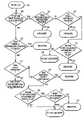
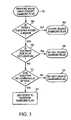
- FIG. 1is a flow chart showing one example of dynamic metrology for “wafer-to-wafer” processing in the present invention.
- FIGS. 2A and 2Bare an illustration of regions on a wafer, with FIG. 2A being a plan view of the wafer and FIG. 2B being a cross-section of the wafer along radius B-B of FIG. 2A .
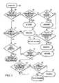
- FIG. 3is a flow chart showing one example of dynamic metrology for “within-wafer” processing in accordance with one or more embodiments of the present invention.
- FIGS. 4A and 4Bare a spiral sampling plan for a wafer for use with one or more embodiments of the invention, with FIG. 4A being a plan view of the wafer and FIG. 4B being a cross-section of the wafer along a radius of FIG. 4A .
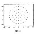
- FIG. 5is an example of another sampling plan for use with one or more embodiments of the invention.
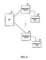
- FIG. 6is a block diagram of a computerized process control system which may be used in connection with one or more embodiments of the present invention.
- static metrologymeans there is a pre-determined sampling plan in connection with a wafer (or other device) to be measured, specifying substantially the same points for each wafer (or the other device).
- a dynamic metrology planutilizes an initial sampling plan and adjusts the sampling responsive to certain events or non-events. As an example of an adjustment due to a non-event, if the last ten wafers measured are all the same, and if the processing device did not change, and if the recipe on the processing device did not change, one could reasonably assume that the next series of wafers will have measurements that are also all the same.
- the inventionprovides for dynamically adjusting the measurements, for example, such that every third wafer instead of every wafer is measured. This invention thus detects and adjusts for not only potential errors, which could arise for example upon a recipe change, but also for accuracy.
- One or more embodiments of the present inventioncontemplate that the invention may be used in connection with wafer-to-wafer measurements described above, as well as, or alternatively, in connection with within-wafer measurements.
- within-wafer measurementsin which measurements are taken along a radius of a 200 mm diameter wafer and the radius is measured in 10 mm increments.
- the systemadjusts to measure another point from the sampling plan between 50 mm and 60 mm to better characterize that variation, or optionally to measure an additional point, for example, between 40 mm and 50 mm that is near the location of the variation.
- the die mapincludes points at 45 mm and 55 mm, these points can then be added as measurement points. Adjusted measurements now encompass in this example, 40 mm, 45 mm, 50 mm, 55 mm, and 60 mm.
- the systemdynamically added the two additional points (in the example) to better characterize the measurement and/or the variation. Where there are provided a number of candidate points in the die map allowing points to be added or substituted, the system can select among the points any of several ways, such as selecting the closest to mean, mode, other statistical analysis, etc.
- a sampling planprovides specific measure points within a die, a die being the section on the wafer that will typically eventually become a single chip after processing. There are specified points within the die that are candidates for measuring.
- the map of the dieis stored, preferably in an electronic format representing the map.
- One appropriate place for storing the die map informationis in the factory automation system (“MES” or manufacturing execution system).
- MESfactory automation system
- the stored die map informationmay be advantageously retrieved and translated to determine the available points for measurement on the wafer.
- an appropriate replacementwould be points selected from the candidate points specified by the die map which are close to or between 45 mm and 55 mm. Those points could be selected dynamically as well. Other criteria may be used for selecting points as well.
- Dynamic metrologyis performed to better meet a certain specification. For example, if recipe parameters are changed on the processing device, to adjust the thickness of a film that is deposited on the wafer, it may be desirable to more closely check whether the specification is still being achieved by performing measurements.
- one or more embodiments of the present inventionadvantageously determine the appropriateness of performing additional measurements when one or more events occur that are likely to indicate an internal or external change affecting the manufacturing process or results.
- the increase in measurements and possible corresponding decrease in processingoccur on an as-needed basis and/or based on predetermined criteria.
- the wafer-to-wafer variation of the inventioncan check for events which may affect a series of wafers and may adjust the sampling plan. For example, during processing, the system determines if an increase is needed in the frequency of wafers measured for process control, for example, based on—1) a change in the processing device the wafers are processed on, 2) a change in the parameters or recipe that were used by the processing device to process the wafer, 3) large detected variations or errors in measurements, and/or 4) a significant run of wafers without errors.
- one or more embodiments of the present inventioncontemplate that the system obtains a stored die map with metrology coordinate information from the MES. As indicated, the system can provide not only for assigning the measurement points optionally dynamically, but also for de-assigning.
- One or more embodiments of the present inventionenvision changing the sampling plan using information that is gathered from the MES and automatically using that new sampling plan, depending on, for example the type of processing device on which the wafers are processed.
- the systemhas stored information about a wafer that indicates, among other things, the type of chip or type of device and an associated sampling plan to be used when measuring a wafer containing a specific device. Based on the type of device, the associated sampling plan or die map can be obtained, where the die map includes a set of candidate metrology points. The system then selects metrology points for the current wafer from the set of, or responsive to, the candidate points in the die map.
- sampling plangeneration of the sampling plan can vary from device to device (chip type to chip type) and some measurements may be based on die distribution on the wafer.
- regionsBy dividing a wafer into regions and using regions of the wafer for measurement, one or more embodiments of the present invention provide flexibility in selecting one or more points from available points in the region. Use of regions is one way to provide a pool of candidate points, from which the system may select points that are most relevant to the desired information about the film on the wafer.
- the systemmay, for example, measure twenty-two to twenty-five points per wafer from the pool of candidate points. For some processes the system might measure fewer points, such as eight points, because it takes longer to measure those points or the wafer—processing time—is faster. For other processes the system might measure one point of another type of property, such dopant concentration, which is a relatively slow measurement.
- Each processing device on which a wafer is processedhas a different processing time, and therefore the selected standard sampling rate may depend on the speed of processing of the processing device and metrology tool.
- measurements on every waferwill not slow down processing since the speed of the processing device is slower than the measurements by the metrology tool.
- polishing and cleaning processing devicesmay consume five minutes or more to process a wafer. In that case a post-processing measurement by the metrology tool on every wafer would often not reduce throughput.
- the systemmay determine whether or not to make additional measurements based on the initial and the final condition of the wafers. For example, if there is a situation in which the incoming thickness profile of a cross section of a wafer does not change very much, the system may reduce the frequency of samples of incoming profiles, wafer-to-wafer. On the other hand, if the incoming profile is changing significantly, it may be desirable to measure every entering wafer.
- FIG. 1illustrating an example of a flow chart for one or more embodiments of a wafer-to-wafer dynamic metrology system.
- the systemchecks whether there may have been a significant change in the state of the processing device, which can be detected by checking, for example, idle time, change of consumables, etc. There may be other events that could be checked that would indicate a potential change in the processing device or lead one to believe that it might have been changed. It is possible that the processing device itself may include sufficient programming to recognize or track those type of events.
- 1includes an example set of events or state changes that initiate analysis and decision-making, based upon information gathered from the processing device and based on a significant internal or external change (e.g., system was idle for a long time, chamber was cleaned, new batch of slurry, initial wafer, etc.). Other events or states may be included in the set from which it is determined whether or not to measure a wafer.
- a significant internal or external changee.g., system was idle for a long time, chamber was cleaned, new batch of slurry, initial wafer, etc.
- Other events or statesmay be included in the set from which it is determined whether or not to measure a wafer.
- One or more embodiments, of the present inventionalso envision the following. Assume that there is provided an initial sampling plan.
- the plancould, for example, direct measuring of specific points on each wafer and/or comprise information indicating which wafers within the lot will be measured.
- the waferis measured according to the sampling plan.
- the systemdeviates from the initial sampling plan when warranted.
- the systemcould return to the initial sampling plan once it detects that the process is again “normal” or again producing product within specification.
- the cassette of wafersarrives at the processing device, usually from some other processing device, and processing on the lot is started, at block 101 .
- a wafer being processed by a processing deviceis the first wafer of a particular lot on the processing device then it may be desirable to measure this wafer, in order to detect if perhaps there was some processing device related property that changed.
- the systemchecks whether it is processing the first wafer on the resource. This could also include situations such as following preventative maintenance where the chamber in the processing device has been cleaned or perhaps a consumable was replaced in the processing device.
- a processed waferwas the first (or other predetermined) wafer on the resource in accordance with block 103 , then the system checks at block 105 whether the processing device was idle, greater than some specified time before starting the present process; and if the processing device was not significantly idle, the system checks at block 107 whether the process was changed or altered. If the process was not changed, a measurement of the wafer may or may not be-implemented according to the initial sampling plan at block 116 the wafer-is accordingly measured at block 120 or not measured at block 118 . On the other hand, if the resource was idle for a sufficiently long time, or if the process has changed, at blocks 109 or 111 respectively, a new measurement is taken.
- the systemchecks whether a significant change was made to the recipe, such as by the process control algorithm or process controller. It is typically desirable to ensure that even if a significant change was made, the specifications are still satisfied. A change to the recipe could include time, pressures, flow rates, etc., or even a completely different recipe. If the recipe was significantly changed, then at block 115 , the system calls for a measurement of the wafer.
- the systemalso checks whether a fault was detected, such as in the processing device.
- Processing devicesmay be monitored by the factory automation system, for example to determine whether there is some problem with the processing device, either from the automation system side or from the processing device itself. Also, the processing device itself may include the ability to detect a fault. If a fault is detected, the system could subsequently measure to confirm that the wafer is within specifications. Thus, at block 117 , it is determined whether a fault was detected. If a fault was detected, at block 123 the system measures the wafer. Since it is likely that the wafer has errors, it might be desirable not to use such measurements for feedback purposes.
- the systemuses the measurement value or stores that measurement value for further processing, such as measurements following a resource idle condition.
- the systemmay check the wafer or series of wafers for acceptability but does not store the value which might skew historical results.
- the systemis using the historical value for modeling of the processing device in order to better predict how the processing device will behave, or for other purposes. For example, where a fault is know to have occurred, the manufacturer will want to find and correct the cause of the fault, often by changing a process component or parameter. Thus, the process data attributed to a wafer that triggered detection of a fault is not indicative of the “normal” processing in the process system.
- the systemmerely ensures that that wafer is a good (e.g., usable) wafer versus a bad wafer.
- a good wafere.g., usable
- the systemusually following a fault there are several wafers in a series potentially affected by the fault, and it is desirable to measure the wafers in the series. Once the wafer(s) are measured following a fault, if the wafer(s) are bad, it is desirable to mark the wafer as questionable and discard the measurement value as well as perhaps the wafer itself.
- the systemchecks whether the previous wafer was sufficiently far from the target, as determined by a previous measurement made in accordance with FIG. 1 . If so, then at block 121 the system measures the current wafer as well.
- the systemchecks the initial sampling plan to advantageously determine whether the current wafer should be measured according to the initial sampling plan. If not, then the system does not measure the wafer.
- a modified sampling planis used to measure the wafer under appropriate situations, such as after a change of type of chip.
- FIG. 2a map of a wafer illustrating measurement regions for the within-wafer dynamic metrology. It is referred to as “within-wafer” since the system may be changing the metrology within the wafer, in distinction to the previously-described wafer-to-wafer dynamic metrology.
- FIG. 3illustrated in detail below, illustrates an example of a flow chart for within-wafer dynamic metrology.
- the process performed by the processing device on the waferis symmetric such that the system is affecting portions of the film on the wafer in a symmetric matter, it may be reasonable to measure fewer points, perhaps a measurement of only one radii.
- information on additional measurement valuesmay need to be captured. The number of desirable measurement points therefore additionally depends upon the type of process, and upon the step in the process if applicable.
- the factory automation systemor the software in the factory automation system, is programmed to determine which process (or processes) or step within a process is being run on which processing device. Based on that information, the system can determine whether few or many points are desired for an adequately precise measurement or set of measurements of the wafer.
- the process control algorithmdescribes four recipe changes.
- the inventiondetermines which wafers need to be measured (wafer-to-wafer), and any desired change in number of measurement points due to the dynamic recipe change (within-wafer).
- This metrology strategyconsequently enables a dynamic metrology change based on the die map from the MES or other factory automation system.
- the die mapprovides a pool of candidate points corresponding to a wafer to be measured, and the system can select from among the candidate points, the points that correspond most directly to the information needed or desired in connection with that wafer.
- the MES or other factory automation systemprovides information indicating allowable or relevant possible points that could be measured; from those candidate points, one or more embodiments of the present invention contemplate that the system selects the minimal set of points that would capture the desired information.
- FIGS. 2A and 2Billustrate a plan view and a cross section of an example of a typical wafer 201 , in this instance having radial regions 1 through 5 .
- the illustrated wafer 201is circular. Chips on the wafer are usually square and placed across the wafer. At the end of processing, the chips are divided from the wafer.
- FIG. 2Bshows a cross section of the wafer of FIG. 2A , across section B-B from one edge to the center of the wafer.
- Region 1extends radially from the center to 40 mm; region 2 extends from 40 mm to 60 mm; region 3 extends from 60 mm to 80 mm; region 4 extends from 80 mm to 92 mm; and region 5 extends from 92 mm to 95 mm.
- a wafercould be divided into more or fewer regions. Also, although the regions are illustrated as radial, the same concepts apply where the regions are neither circular nor radial.
- a die mapincludes a sampling plan that optionally distinguishes among different regions of the wafer.
- Such a sampling planwould include information indicating a set of measurement points, associated with regions of the wafer.
- FIG. 3discusses an example of within-wafer metrology, that is, when the system should or should not change the measurement points.
- FIG. 3thus contrasts to FIG. 1 , indicating whether to measure a current wafers (wafer-to-wafer dynamic metrology).
- FIG. 3defines an example set of questions to determine whether more points are needed to measure a region variation within a given wafer.
- the waferis measured by the metrology tool utilizing the current sampling plan. Having-measured the wafer, the system analyzes the current wafer to determine whether there are significant variations that might warrant changing the sampling plan for the next wafer. The wafers are potentially changed from run to run. That is, the system performs an action, and then based upon the results of that action, the system determines whether to utilize the same sampling plan for the next wafer or to do something different.
- an outlier or flieris a situation in which the measurement point is not an accurate reflection of the actual value. If there is a speck of dust on the wafer, for example, this may cause an erroneous thickness measurement; or for instance the actual measured point may be significantly distant from the correct measurement coordinates, resulting in significantly higher or lower thickness.
- An outlier or fliercan be determined statistically in a number of ways based on how different the measured point is from the expected measurement. It may be difficult to determine in some cases whether the variation is due to a flier or if there is an actual variation. The data collected could be used to indicate a potentially defective die.
- the sampling planis not changed.
- the measurementis not likely to be an accurate reflection of the wafer, and therefore the system should not react to the measurement.
- the variation from the specificationis one for which the processing device can possibly compensate. For example, a processing device may be able to correct for radial variation, but not for a variation that is angular or azimuthal.
- the sampling planis not changed.
- the processing devicecan compensate for the variation in the region, then at block 315 points are added to the region in the sampling plan for the next wafer in order to better characterize the region.
- the datamay be fed back to system controller in order to change the process in response to this drift condition.
- an error in one or more wafersmay initiate some level of error handling and/or alarming. If there is an error that does not result in a change to the sampling plan, such as a non-systematic variation, and even if the system cannot compensate, in one or more embodiments of the present invention the system might generate an alarm or trigger performance of other error handling. If the error exhibits the characteristics of a systematic effect, such as wafers out of specification, then an alarm could be generated. If the error is one wafer that is out of specification, according to one or more embodiments of the invention, the system flags that wafer.
- the flow chart of FIG. 3illustrates one potential example of within-wafer metrology.
- Other types of checks and decisionsare also contemplated and may be used in combination with, and/or replace, the detailed checks.
- an additional checkcould include whether there is a large change in the recipe parameter that could have affected a specific region; if so, a determination can be made as to whether the change affected the region to the extent that more information is desirable; and if so, more metrology points can be added to the sampling plan.
- FIGS. 4A and 4Billustrating a plan view and sectional view, respectively, of a triangular spiral sampling plan.
- Thisis one example of a specific sampling plan, showing specific measurement points 401 in relation to a wafer 201 .
- Other static sampling plansmay be used.
- the illustrated spiral sampling planis well adapted to capturing both radial change as well as angular change.
- Ris the radius and theta is the-angle
- the triangular spiral sampling plancan capture variations in both the R direction and the theta direction. If the system can compensate only for variations that are radial, it may be desirable to add measurement points in the radial direction. Even if a significant angular variation was detected, one might not add any measurement points if the variation cannot be corrected anyway due to the manner of holding and/or spinning the wafer in the processing device.
- the points 401are distributed along three splines 403 radiating from the center of the wafer.
- the points 401 of this exampleare generally distributed in each of eight regions, shown in FIG. 4B .
- Region 1which are all points radially from approximately 0 mm to 40 mm, there is a large variation; more measurement points could be added from the die map in order to better characterize that variation.
- 4Aindicates equidistant radii at 24.375 mm from the center, 48.75 mm, 73.125 mm, and 97.5 mm for purposes of illustration. It should be noted that the distance between points 401 along spline 403 advantageously decreases towards the outer diameter of the wafer, to accommodate the increase in the surface area in relation to the width of the region.
- FIGS. 4A and 4Billustrate only one of many potential sampling plans, in this instance a particular spiral sampling plan. Other sampling plans are possible.
- One advantage of the illustrated spiral sampling planis that it quantifies not only radial but also angular variation.
- Another advantageis that it also measures a weighted region, that is it measures a selected number of coordinates in approximate proportion to the wafer surface area that they represent. Closer to the edge of the wafer, measurement points are more dense or closer together, since the radial distance is much further and the area of the region is greater in comparison to the width of the region.
- the variation on the edgetypically will be much higher than variation toward the center of the wafer.
- the variationtends to increase proportionately further away from the-center.
- the density of the points to be measuredmay be advantageously increased as the points move radially outward.
- the present inventionoptionally optimizes the measuring speed of the spiral sampling plan.
- a measurementis faster if performed radially across the wafer.
- the wafermay be rotated approximately 120 degrees subsequent to a linear measurement, and then the next measurement is taken at the next point positioned radially across the wafer; then the wafer is again rotated approximately 120 degrees for the next measurement and so forth.
- the angle of rotationcan be varied to correspond to the disposition of points as well as to accommodate the capabilities and/or limitations of the metrology tool.
- the wafermay be positioned on a pedestal and rotated and shifted while the metrology tool performs the measurement of the wafer.
- sampling plansare also contemplated by one or more embodiments of the present invention, including a sampling plan with a large number of points, such as forty-nine (illustrated in FIG. 5 ), or a small number of points, such as five.
- Other sampling plans with other distributions of metrology points, such as distributed in concentric circles or star formations, or other variationsmay be used in one or more embodiments.
- FIG. 6illustrating a possible computerized process control system which may be used in connection with one or more embodiments of the present invention.
- the systemincludes a standard factory automation system such as an APC 601 .
- the APC 601provides for central control of, and communication with, one or more standard processing devices 603 or resources.
- the processing device 603communicates with and controls a standard metrology tool 605 , which measures wafers in accordance with the processes described in connection with the present invention.
- FIG. 6illustrates a typical system, other configurations are possible, such as having the metrology device(s) 605 communicate with the APC 601 , or even omitting the APC 601 and having the metrology device 605 pattern the processes described herein.
- processing devicesexamples include chemical mechanical planarization (CMP) tools, etch tools, chemical vapor deposition (CVD) tools, lithography tools and others. It should be noted that the processing device may incorporate the metrology tool in some configurations.
- CMPchemical mechanical planarization
- CVDchemical vapor deposition
- sampling planmay include information in addition to that mentioned above. Further, a sampling plan may combine information from multiple sampling plans. As another example, although the above discusses a predetermined or static sampling plan, such predetermined or static sampling plan includes those sets of coordinate points measured on the fly such as just prior to wafer processing.
- events or conditions in addition to, in combination with, and/or replacing these discussed abovecould be checked as part of the wafer-to-wafer metrology determination.
- a metrology tool, a processing device, or the system itselfcould indicate a fault.
- the reason for the faultcould be indicated, and such information could be specifically checked and appropriately handled as well.
- the systemcould check for changes to the recipe in several different ways, such as replacement of a recipe, or change in recipe parameters.
- the factory automation systemmay be a general purpose computer, or a specially programmed special purpose computer. It may also be implemented as a distributed computer system rather than as a single computer; some of the distributed system might include embedded systems. Further, the programming may be distributed among processing devices and metrology tools or other parts of the process control system. Similarly, the processing could be controlled by a software program on one or more computer systems or processors, or could be partially or wholly implemented in hardware. Moreover, the factory automation system may communicate directly or indirectly with the relevant metrology tool(s), processing devices, and metrology system(s); or the metrology tool(s), processing devices and metrology system(s) may communicate directly or indirectly with each other and the factory automation system.
Landscapes
- Engineering & Computer Science (AREA)
- Manufacturing & Machinery (AREA)
- Physics & Mathematics (AREA)
- General Physics & Mathematics (AREA)
- Mechanical Engineering (AREA)
- Automation & Control Theory (AREA)
- Microelectronics & Electronic Packaging (AREA)
- Power Engineering (AREA)
- Computer Hardware Design (AREA)
- Condensed Matter Physics & Semiconductors (AREA)
- Quality & Reliability (AREA)
- General Engineering & Computer Science (AREA)
- Human Computer Interaction (AREA)
- Testing Or Measuring Of Semiconductors Or The Like (AREA)
Abstract
Description
- This application is a divisional of U.S. patent application Ser. No. 10/135,451, now U.S. Pat. No. ______, filed May 1, 2002, which claims the benefit of U.S. Provisional Application Ser. No. 60/322,459, filed Sep. 17, 2001, which is expressly incorporated herein by reference; and U.S. Provisional Application Ser. No. 60/298,878, filed Jun. 19, 2001, which is expressly incorporated herein by reference.
- 1. Field of the Invention
- The present invention concerns computer-related and/or assisted methods, systems and computer readable mediums for metrology during process control. More specifically, it relates to dynamic adjustment of metrology schemes and sampling during advanced process control methods, for example during control of semiconductor technology manufacture.
- 2. Related Art
- in the wafer fabrication art, measurements are made by metrology tools on wafers as they are being manufactured by processing devices, in order to ensure that the wafers are produced according to a predefined specification. The measurements are made of physical properties such as film thickness and uniformity, dopant concentration, gate length and critical dimension. This is known as the science of “metrology.”
- Measurements to be made are typically specified in a “die map”. The die map indicates where the different chips (or die) are located on a wafer (in the typical situation where multiple chips are formed on and eventually cut from a single wafer), as well as significant locations, such as corners, on each die. In order to measure the right hand corner on each die, for example, multiple points are measured on the wafer in accordance with the die map. Ordinarily a die map is a digital representation of coordinate points, or “metrology coordinates,” on the wafer.
- The metrology coordinates are usually provided by an engineer, and vary depending on the engineer's preferences. Metrology coordinates are conventionally provided as x, y coordinates.
- A “sampling plan,” alternatively referred to as a “metrology plan,” contains metrology coordinates drawn from the die map. The sampling plan denotes a specific plan for taking certain measurements. These measurements may include some or all of the possible points and/or chips in the die map.
- A conventional metrology system assigns a sampling plan that predetermines which wafers are to be measured in connection with a processing device, and the measurements which are to be taken of those wafers by the metrology tool. For example, the sampling plan might define that each fifth wafer should be measured at pre-designated locations. These sampling plans are not changed after being initially assigned, and hence the metrology systems are static.
- Unfortunately, manufacturing results tend to drift away from the intended target or specification when there is a change in the manufacturing process, such as a change in recipe, preventative maintenance, consumables change, environmental change or a new lot of wafers. Conventional metrology systems tend to miss some wafers which are outside specification limits, since these systems use a virtually consistent measurement scheme, having consistently frequent measurements with consistent spatial resolution, without taking into consideration whether any changes were introduced into the manufacturing process which might change the manufacturing results.
- Manufacturing systems do not typically call for a measurement of every wafer, since measuring takes time and increasing the number of measurements results in a decrease of productivity. On the other hand, measuring fewer wafers tends to lead to delayed detection of critical information for process control that may significantly impact wafer yield. While conventional sampling systems will sample wafers during and/or after production, these systems do not adjust the initially assigned sampling plan for the wafers during production.
- Thus, there remains a need for dynamic metrology to improve the quality of products. For semiconductor wafers, there remains a need to better check whether each specification is met under production conditions. There also remains a need to respond to a change in parameters which may cause a variance from intended target results, such as recipe parameters, and to adjust the frequency and/or spatial resolution of measurements. Unfortunately, taking measurements takes time, and most processing devices are faster than the measurements that need to be taken by metrology tools in order to characterize the wafers using a metrology. Thus, there remains a need for a method, system and medium to react to changes potentially affecting the system results, and to appropriately adjust, increase, or decrease the measurements accordingly.
- The present invention alleviates the problems of the conventional techniques described above by dynamically determining whether a wafer needs to be measured for process control based on changes in the resources, recipes, etc. In addition, for a given wafer to be measured, measuring points are also dynamically assigned to the metrology tool.
- More specifically, two variations of embodiments of the present invention are contemplated and may be used independently or together. According to the first variation, the frequency at which wafers are measured (“wafer-to-wafer”) is adjusted, following an event that suggests that more (or fewer) wafers should be measured. According to the second variation, the spatial resolution of the measurements of those wafers selected for measurement (“within-wafer”) is increased or decreased, following an event that suggests each wafer which is measured should be measured in greater (or lesser) detail.
- In one or more embodiments of the present invention, candidate coordinate measurement points are mapped in a die map, and a subset of the candidate coordinate measurement points are selected as the initial points where measurements are to be made. Subsequently, according to the within-wafer variation, the invention dynamically selects more, fewer or different points (depending on the circumstances) to be measured from among the candidate coordinate measurement points. According to the wafer-to-wafer variation, when there is a change in the manufacturing process, the number of measurements may be increased, to measure every wafer rather than just every third wafer for example. As one example, when a new recipe is implemented to significantly change the thickness at a particular region on the wafer, a greater number of within-wafer measurements can be made at that location by selecting more and/or different candidate measurement points. As another example, when a fault is detected, the frequency of wafers selected for measurement is increased; this increases the probability of detecting defectively manufactured wafers and correcting the control parameters (such as in connection with a feed forward/feedback method). In some situations, large deviations may require less frequent measurement or less spatial resolution than small deviations when the large deviations clearly identify the problem, whereas small deviations may be difficult to identify and more frequent and/or dense measurements may be necessary. The reverse may be appropriate in other situations regarding the frequency and density of measurements, or it may be the case that the same number of measurements may be taken regardless of deviation.
- According to one or more embodiments of the present invention, there is provided a method, system and/or computer-implemented method for measuring at least one manufacturing characteristic for at least one product manufactured by a manufacturing process. Information is provided, representative of a set of candidate points to be measured by the manufacturing process on the at least one product. The manufacturing process executes a plan for performing measurements on the at least one product to measure the at least one manufacturing characteristic, the plan defining the measurements to be made responsive to the set of candidate points. A change in the manufacturing process is detected, the change including at least one of: receiving new material in the manufacturing process, detecting a fault in the manufacturing process, detecting a change in a control parameter in the manufacturing process, and detecting a variation in a measurement of the at least one product.
- According to one or more embodiments, the plan for performing measurements is adjusted on the detected change and at least one additional measurement is performed responsive thereto.
- According to one or more embodiments, the measurements of the plan are adjusted wafer-to-wafer and/or within-wafer.
- According to one or more embodiments, the product is a semi-conductor wafer and the manufacturing process is an automated semi-conductor manufacturing process.
- According to one or more embodiments, the plan further includes information representative of a metrology recipe.
- According to one or more embodiments, the candidate points are included in a map corresponding to the at least one product. The plan may be a pre-determined sampling plan.
- According to one or more embodiments, the plan defines at least one region on each of the candidate points corresponding to the at least one region.
- According to one or more embodiments, the adjustment includes determining the at least one region corresponding to the detected change, selecting the at least one additional measurement responsive to the candidate points corresponding to the determined region, assigning the selected at least one additional measurement to be performed under the plan, and revising at least one of the measurements, the additional measurement and the plan. The adjustment may include determining whether the detected change may affect a series of products, and if so, determining whether to measure at least one of the products in the series of products. The products may be provided in a group, and the plan may further include first information representative of the products in the group that are available to be measured, and second information representative of the products in the group that are to be measured under the plan.
- According to one or more embodiments, information representative of measurement results on the product is discarded when the measurements results indicate a variation in measurement of the product and/or when a fault is detected in the manufacturing process.
- According to one or more embodiments, the sampling plan includes a plurality of splines radiating from a center of a product, and the candidate points are distributed along the splines. The distribution of the candidate points along the splines may be weighted according to a surface area of the product. According to one or more other embodiments, the sampling plan includes a plurality of radially distributed candidate points.
- The above mentioned and other advantages and features of the present invention will become more readily apparent from the following detailed description in the accompanying drawing, in which:
FIG. 1 is a flow chart showing one example of dynamic metrology for “wafer-to-wafer” processing in the present invention.FIGS. 2A and 2B are an illustration of regions on a wafer, withFIG. 2A being a plan view of the wafer andFIG. 2B being a cross-section of the wafer along radius B-B ofFIG. 2A .FIG. 3 is a flow chart showing one example of dynamic metrology for “within-wafer” processing in accordance with one or more embodiments of the present invention.FIGS. 4A and 4B are a spiral sampling plan for a wafer for use with one or more embodiments of the invention, withFIG. 4A being a plan view of the wafer andFIG. 4B being a cross-section of the wafer along a radius ofFIG. 4A .FIG. 5 is an example of another sampling plan for use with one or more embodiments of the invention.FIG. 6 is a block diagram of a computerized process control system which may be used in connection with one or more embodiments of the present invention.- The following detailed description includes many specific details. The inclusion of such details is for the purpose of illustration only and should not be understood to limit the invention. Throughout this discussion, similar elements are referred to by similar numbers in the various figures for ease of reference. In addition, features in one embodiment may be combined with features in other embodiments of the invention.
- In one or more embodiments of the present invention, static metrology means there is a pre-determined sampling plan in connection with a wafer (or other device) to be measured, specifying substantially the same points for each wafer (or the other device). In contrast, a dynamic metrology plan utilizes an initial sampling plan and adjusts the sampling responsive to certain events or non-events. As an example of an adjustment due to a non-event, if the last ten wafers measured are all the same, and if the processing device did not change, and if the recipe on the processing device did not change, one could reasonably assume that the next series of wafers will have measurements that are also all the same. That being the case, then in order to increase throughput and decrease the time it takes to do measurements, the invention provides for dynamically adjusting the measurements, for example, such that every third wafer instead of every wafer is measured. This invention thus detects and adjusts for not only potential errors, which could arise for example upon a recipe change, but also for accuracy.
- One or more embodiments of the present invention contemplate that the invention may be used in connection with wafer-to-wafer measurements described above, as well as, or alternatively, in connection with within-wafer measurements. Consider an example of within-wafer measurements, in which measurements are taken along a radius of a 200 mm diameter wafer and the radius is measured in 10 mm increments. During processing it is noted or detected by the usual detection process that there is a large variation at the 50 mm and 60 mm points. For the next sample, the system adjusts to measure another point from the sampling plan between 50 mm and 60 mm to better characterize that variation, or optionally to measure an additional point, for example, between 40 mm and 50 mm that is near the location of the variation. If the die map includes points at 45 mm and 55 mm, these points can then be added as measurement points. Adjusted measurements now encompass in this example, 40 mm, 45 mm, 50 mm, 55 mm, and 60 mm. The system dynamically added the two additional points (in the example) to better characterize the measurement and/or the variation. Where there are provided a number of candidate points in the die map allowing points to be added or substituted, the system can select among the points any of several ways, such as selecting the closest to mean, mode, other statistical analysis, etc.
- A sampling plan provides specific measure points within a die, a die being the section on the wafer that will typically eventually become a single chip after processing. There are specified points within the die that are candidates for measuring. The map of the die is stored, preferably in an electronic format representing the map. One appropriate place for storing the die map information is in the factory automation system (“MES” or manufacturing execution system). The stored die map information may be advantageously retrieved and translated to determine the available points for measurement on the wafer. Referring back to the previous example proposing measurement points on the radius at 45 mm and 55 mm, if these specific points are not relevant to the current die (e.g., they are not specified by the die map), an appropriate replacement would be points selected from the candidate points specified by the die map which are close to or between 45 mm and 55 mm. Those points could be selected dynamically as well. Other criteria may be used for selecting points as well.
- Dynamic metrology is performed to better meet a certain specification. For example, if recipe parameters are changed on the processing device, to adjust the thickness of a film that is deposited on the wafer, it may be desirable to more closely check whether the specification is still being achieved by performing measurements.
- In order to avoid slowing down the process, one or more embodiments of the present invention advantageously determine the appropriateness of performing additional measurements when one or more events occur that are likely to indicate an internal or external change affecting the manufacturing process or results. The increase in measurements and possible corresponding decrease in processing occur on an as-needed basis and/or based on predetermined criteria.
- The wafer-to-wafer variation of the invention, for example, can check for events which may affect a series of wafers and may adjust the sampling plan. For example, during processing, the system determines if an increase is needed in the frequency of wafers measured for process control, for example, based on—1) a change in the processing device the wafers are processed on, 2) a change in the parameters or recipe that were used by the processing device to process the wafer, 3) large detected variations or errors in measurements, and/or 4) a significant run of wafers without errors.
- Particularly regarding within-wafer variation, one or more embodiments of the present invention contemplate that the system obtains a stored die map with metrology coordinate information from the MES. As indicated, the system can provide not only for assigning the measurement points optionally dynamically, but also for de-assigning.
- One or more embodiments of the present invention envision changing the sampling plan using information that is gathered from the MES and automatically using that new sampling plan, depending on, for example the type of processing device on which the wafers are processed. Advantageously, the system has stored information about a wafer that indicates, among other things, the type of chip or type of device and an associated sampling plan to be used when measuring a wafer containing a specific device. Based on the type of device, the associated sampling plan or die map can be obtained, where the die map includes a set of candidate metrology points. The system then selects metrology points for the current wafer from the set of, or responsive to, the candidate points in the die map.
- With respect to the sampling plan, generation of the sampling plan can vary from device to device (chip type to chip type) and some measurements may be based on die distribution on the wafer. By dividing a wafer into regions and using regions of the wafer for measurement, one or more embodiments of the present invention provide flexibility in selecting one or more points from available points in the region. Use of regions is one way to provide a pool of candidate points, from which the system may select points that are most relevant to the desired information about the film on the wafer.
- In practice, the system may, for example, measure twenty-two to twenty-five points per wafer from the pool of candidate points. For some processes the system might measure fewer points, such as eight points, because it takes longer to measure those points or the wafer—processing time—is faster. For other processes the system might measure one point of another type of property, such dopant concentration, which is a relatively slow measurement.
- In any event, it is important to balance the time consumed in a measurement against the need to produce quality products. Manufacturers consider it to be more important to be within specifications and not produce defective product, than to rapidly produce product of suspect qualities.
- Each processing device on which a wafer is processed has a different processing time, and therefore the selected standard sampling rate may depend on the speed of processing of the processing device and metrology tool. On some processing devices, measurements on every wafer will not slow down processing since the speed of the processing device is slower than the measurements by the metrology tool. For example, polishing and cleaning processing devices may consume five minutes or more to process a wafer. In that case a post-processing measurement by the metrology tool on every wafer would often not reduce throughput.
- Additionally, the system may determine whether or not to make additional measurements based on the initial and the final condition of the wafers. For example, if there is a situation in which the incoming thickness profile of a cross section of a wafer does not change very much, the system may reduce the frequency of samples of incoming profiles, wafer-to-wafer. On the other hand, if the incoming profile is changing significantly, it may be desirable to measure every entering wafer.
- Reference is made to
FIG. 1 , illustrating an example of a flow chart for one or more embodiments of a wafer-to-wafer dynamic metrology system. The system checks whether there may have been a significant change in the state of the processing device, which can be detected by checking, for example, idle time, change of consumables, etc. There may be other events that could be checked that would indicate a potential change in the processing device or lead one to believe that it might have been changed. It is possible that the processing device itself may include sufficient programming to recognize or track those type of events. The flowchart example inFIG. 1 includes an example set of events or state changes that initiate analysis and decision-making, based upon information gathered from the processing device and based on a significant internal or external change (e.g., system was idle for a long time, chamber was cleaned, new batch of slurry, initial wafer, etc.). Other events or states may be included in the set from which it is determined whether or not to measure a wafer. - One or more embodiments, of the present invention also envision the following. Assume that there is provided an initial sampling plan. The plan could, for example, direct measuring of specific points on each wafer and/or comprise information indicating which wafers within the lot will be measured. The wafer is measured according to the sampling plan. According to the wafer-to-wafer metrology plan, the system deviates from the initial sampling plan when warranted. The system could return to the initial sampling plan once it detects that the process is again “normal” or again producing product within specification.
- Referring still to
FIG. 1 , consider for example a typical cassette of twenty-five wafers to be processed according to one or more embodiments of the present invention. The cassette of wafers arrives at the processing device, usually from some other processing device, and processing on the lot is started, atblock 101. - If a wafer being processed by a processing device is the first wafer of a particular lot on the processing device then it may be desirable to measure this wafer, in order to detect if perhaps there was some processing device related property that changed. Thus, at
block 103, the system checks whether it is processing the first wafer on the resource. This could also include situations such as following preventative maintenance where the chamber in the processing device has been cleaned or perhaps a consumable was replaced in the processing device. - If a processed wafer was the first (or other predetermined) wafer on the resource in accordance with
block 103, then the system checks atblock 105 whether the processing device was idle, greater than some specified time before starting the present process; and if the processing device was not significantly idle, the system checks atblock 107 whether the process was changed or altered. If the process was not changed, a measurement of the wafer may or may not be-implemented according to the initial sampling plan atblock 116 the wafer-is accordingly measured atblock 120 or not measured atblock 118. On the other hand, if the resource was idle for a sufficiently long time, or if the process has changed, atblocks - If the wafer was not the first one on the processing device, then as indicated, at
block 113, the system checks whether a significant change was made to the recipe, such as by the process control algorithm or process controller. It is typically desirable to ensure that even if a significant change was made, the specifications are still satisfied. A change to the recipe could include time, pressures, flow rates, etc., or even a completely different recipe. If the recipe was significantly changed, then atblock 115, the system calls for a measurement of the wafer. - The system also checks whether a fault was detected, such as in the processing device. Processing devices may be monitored by the factory automation system, for example to determine whether there is some problem with the processing device, either from the automation system side or from the processing device itself. Also, the processing device itself may include the ability to detect a fault. If a fault is detected, the system could subsequently measure to confirm that the wafer is within specifications. Thus, at
block 117, it is determined whether a fault was detected. If a fault was detected, atblock 123 the system measures the wafer. Since it is likely that the wafer has errors, it might be desirable not to use such measurements for feedback purposes. - There may be two cases for uses of measurement values. In the first case, the system uses the measurement value or stores that measurement value for further processing, such as measurements following a resource idle condition. In the second case, such as following a fault detection, the system may check the wafer or series of wafers for acceptability but does not store the value which might skew historical results. In the first case, the system is using the historical value for modeling of the processing device in order to better predict how the processing device will behave, or for other purposes. For example, where a fault is know to have occurred, the manufacturer will want to find and correct the cause of the fault, often by changing a process component or parameter. Thus, the process data attributed to a wafer that triggered detection of a fault is not indicative of the “normal” processing in the process system. On the other hand, for the fault detection case, the system merely ensures that that wafer is a good (e.g., usable) wafer versus a bad wafer. Unfortunately, usually following a fault there are several wafers in a series potentially affected by the fault, and it is desirable to measure the wafers in the series. Once the wafer(s) are measured following a fault, if the wafer(s) are bad, it is desirable to mark the wafer as questionable and discard the measurement value as well as perhaps the wafer itself.
- Similarly, if a wafer is off target despite no change to the recipe, no detection of a fault, and no other likely cause of error, there is likely to be a series of off-target wafers. Consequently, where a wafer with errors is detected, the next wafer is significantly more likely to also experience errors. Thus, at
block 119, the system checks whether the previous wafer was sufficiently far from the target, as determined by a previous measurement made in accordance withFIG. 1 . If so, then atblock 121 the system measures the current wafer as well. - Finally, it may be desirable to measure the wafer according to the initial sampling plan. Thus, at
block 125, the system checks the initial sampling plan to advantageously determine whether the current wafer should be measured according to the initial sampling plan. If not, then the system does not measure the wafer. According to one or more embodiments, a modified sampling plan is used to measure the wafer under appropriate situations, such as after a change of type of chip. - Similarly, if no conditions affecting wafer processing are changed, and if the series of wafers have been on target, one would expect the wafers to continue to be on target. Thus, as indicated at
block 127, if the measurement of the last n wafers were sufficiently on target, there is no need to measure the wafer in this instance or as frequently. In this manner, the number of measurements can be reduced and processing time is potentially reduced. On the other hand, if atblock 127 the system determines that the last series of n wafers were not on target, atblock 129 the system measures the current wafer. - Reference is made to
FIG. 2 , a map of a wafer illustrating measurement regions for the within-wafer dynamic metrology. It is referred to as “within-wafer” since the system may be changing the metrology within the wafer, in distinction to the previously-described wafer-to-wafer dynamic metrology. (FIG. 3 , described in detail below, illustrates an example of a flow chart for within-wafer dynamic metrology.) - Where the process performed by the processing device on the wafer is symmetric such that the system is affecting portions of the film on the wafer in a symmetric matter, it may be reasonable to measure fewer points, perhaps a measurement of only one radii. On the other hand, where there were previous steps performed by the processing device on the wafer that were asymmetric, information on additional measurement values may need to be captured. The number of desirable measurement points therefore additionally depends upon the type of process, and upon the step in the process if applicable.
- For instance, given a very uniform process, perhaps only five points on the wafer need to be measured to provide sufficient precision. On the other hand, given a very non-uniform process or much unresolved information, perhaps twenty-five points should be measured to achieve a sufficient level of precision.
- Typically the factory automation system, or the software in the factory automation system, is programmed to determine which process (or processes) or step within a process is being run on which processing device. Based on that information, the system can determine whether few or many points are desired for an adequately precise measurement or set of measurements of the wafer.
- Consider, for example, a processing device with multiple chambers or resources independently processing wafers. In this example, the process control algorithm describes four recipe changes. The invention determines which wafers need to be measured (wafer-to-wafer), and any desired change in number of measurement points due to the dynamic recipe change (within-wafer). This metrology strategy consequently enables a dynamic metrology change based on the die map from the MES or other factory automation system.
- The die map provides a pool of candidate points corresponding to a wafer to be measured, and the system can select from among the candidate points, the points that correspond most directly to the information needed or desired in connection with that wafer. The MES or other factory automation system provides information indicating allowable or relevant possible points that could be measured; from those candidate points, one or more embodiments of the present invention contemplate that the system selects the minimal set of points that would capture the desired information.
FIGS. 2A and 2B illustrate a plan view and a cross section of an example of atypical wafer 201, in this instance havingradial regions 1 through5. As shown inFIG. 2A , the illustratedwafer 201 is circular. Chips on the wafer are usually square and placed across the wafer. At the end of processing, the chips are divided from the wafer.FIG. 2B shows a cross section of the wafer ofFIG. 2A , across section B-B from one edge to the center of the wafer.Region 1 extends radially from the center to 40 mm;region 2 extends from 40 mm to 60 mm;region 3 extends from 60 mm to 80 mm;region 4 extends from 80 mm to 92 mm; andregion 5 extends from 92 mm to 95 mm. A wafer could be divided into more or fewer regions. Also, although the regions are illustrated as radial, the same concepts apply where the regions are neither circular nor radial.- A die map includes a sampling plan that optionally distinguishes among different regions of the wafer. Such a sampling plan would include information indicating a set of measurement points, associated with regions of the wafer.
- The flowchart of
FIG. 3 discusses an example of within-wafer metrology, that is, when the system should or should not change the measurement points.FIG. 3 thus contrasts toFIG. 1 , indicating whether to measure a current wafers (wafer-to-wafer dynamic metrology).FIG. 3 defines an example set of questions to determine whether more points are needed to measure a region variation within a given wafer. - Reference is now made to
FIG. 3 , illustrating an example of the within-wafer dynamic metrology, as contemplated by one or more embodiments of the present invention. Atblock 301, the wafer is measured by the metrology tool utilizing the current sampling plan. Having-measured the wafer, the system analyzes the current wafer to determine whether there are significant variations that might warrant changing the sampling plan for the next wafer. The wafers are potentially changed from run to run. That is, the system performs an action, and then based upon the results of that action, the system determines whether to utilize the same sampling plan for the next wafer or to do something different. - At
block 303, it is determined whether there is a variation from the specification within one or more of the regions on the current wafer. If not, then as indicated byblock 305 there is no need to add more sampling points. - At
block 307, if there was a variation in a region, it is then determined whether the variation was due to an outlier or flier. An outlier or flier is a situation in which the measurement point is not an accurate reflection of the actual value. If there is a speck of dust on the wafer, for example, this may cause an erroneous thickness measurement; or for instance the actual measured point may be significantly distant from the correct measurement coordinates, resulting in significantly higher or lower thickness. An outlier or flier can be determined statistically in a number of ways based on how different the measured point is from the expected measurement. It may be difficult to determine in some cases whether the variation is due to a flier or if there is an actual variation. The data collected could be used to indicate a potentially defective die. - Of course, it should be understood that one or more embodiments of the present invention contemplate that any number of other causes for variations can be detected, and a decision made accordingly as to whether (and how) the sampling plan may be changed.
- Referring still to
FIG. 3 , if the variation from the specification is due to an outlier or flier, then as indicated byblock 309, the sampling plan is not changed. The measurement is not likely to be an accurate reflection of the wafer, and therefore the system should not react to the measurement. - At
block 311, it is determined whether the variation from the specification is one for which the processing device can possibly compensate. For example, a processing device may be able to correct for radial variation, but not for a variation that is angular or azimuthal. Thus, atblock 313, if the processing device cannot compensate for the variation in the region, then the sampling plan is not changed. On the other hand, if the processing device can compensate for the variation in the region, then atblock 315 points are added to the region in the sampling plan for the next wafer in order to better characterize the region. Optionally, the data may be fed back to system controller in order to change the process in response to this drift condition. - According to one or more embodiments of the inventions, an error in one or more wafers may initiate some level of error handling and/or alarming. If there is an error that does not result in a change to the sampling plan, such as a non-systematic variation, and even if the system cannot compensate, in one or more embodiments of the present invention the system might generate an alarm or trigger performance of other error handling. If the error exhibits the characteristics of a systematic effect, such as wafers out of specification, then an alarm could be generated. If the error is one wafer that is out of specification, according to one or more embodiments of the invention, the system flags that wafer.
- The flow chart of
FIG. 3 illustrates one potential example of within-wafer metrology. Other types of checks and decisions are also contemplated and may be used in combination with, and/or replace, the detailed checks. For example, an additional check could include whether there is a large change in the recipe parameter that could have affected a specific region; if so, a determination can be made as to whether the change affected the region to the extent that more information is desirable; and if so, more metrology points can be added to the sampling plan. - Reference is now made to
FIGS. 4A and 4B , illustrating a plan view and sectional view, respectively, of a triangular spiral sampling plan. This is one example of a specific sampling plan, showingspecific measurement points 401 in relation to awafer 201. Other static sampling plans may be used. Nevertheless, the illustrated spiral sampling plan is well adapted to capturing both radial change as well as angular change. Consider polar coordinates, where R is the radius and theta is the-angle; the triangular spiral sampling plan can capture variations in both the R direction and the theta direction. If the system can compensate only for variations that are radial, it may be desirable to add measurement points in the radial direction. Even if a significant angular variation was detected, one might not add any measurement points if the variation cannot be corrected anyway due to the manner of holding and/or spinning the wafer in the processing device. - Still referring to the example sampling plan illustrated in
FIGS. 4A and 4B , thepoints 401 are distributed along threesplines 403 radiating from the center of the wafer. Thepoints 401 of this example are generally distributed in each of eight regions, shown inFIG. 4B . In this sampling plan one could potentially add points in a radial direction. There could be provided more or fewer regions in other embodiments of the invention. Suppose that inRegion 1, which are all points radially from approximately 0 mm to 40 mm, there is a large variation; more measurement points could be added from the die map in order to better characterize that variation.FIG. 4A indicates equidistant radii at 24.375 mm from the center, 48.75 mm, 73.125 mm, and 97.5 mm for purposes of illustration. It should be noted that the distance betweenpoints 401 alongspline 403 advantageously decreases towards the outer diameter of the wafer, to accommodate the increase in the surface area in relation to the width of the region. FIGS. 4A and 4B illustrate only one of many potential sampling plans, in this instance a particular spiral sampling plan. Other sampling plans are possible. One advantage of the illustrated spiral sampling plan is that it quantifies not only radial but also angular variation. Another advantage is that it also measures a weighted region, that is it measures a selected number of coordinates in approximate proportion to the wafer surface area that they represent. Closer to the edge of the wafer, measurement points are more dense or closer together, since the radial distance is much further and the area of the region is greater in comparison to the width of the region.- Moreover, the variation on the edge typically will be much higher than variation toward the center of the wafer. The variation tends to increase proportionately further away from the-center. As a result, the density of the points to be measured may be advantageously increased as the points move radially outward.
- Furthermore, the present invention optionally optimizes the measuring speed of the spiral sampling plan. In performance of metrology, a measurement is faster if performed radially across the wafer. According to the spiral sampling plan contemplated by one or more embodiments of the present invention, the wafer may be rotated approximately 120 degrees subsequent to a linear measurement, and then the next measurement is taken at the next point positioned radially across the wafer; then the wafer is again rotated approximately 120 degrees for the next measurement and so forth. The angle of rotation can be varied to correspond to the disposition of points as well as to accommodate the capabilities and/or limitations of the metrology tool. The wafer may be positioned on a pedestal and rotated and shifted while the metrology tool performs the measurement of the wafer.
- Other sampling plans are also contemplated by one or more embodiments of the present invention, including a sampling plan with a large number of points, such as forty-nine (illustrated in
FIG. 5 ), or a small number of points, such as five. Other sampling plans with other distributions of metrology points, such as distributed in concentric circles or star formations, or other variations may be used in one or more embodiments. - Reference is made to
FIG. 6 , illustrating a possible computerized process control system which may be used in connection with one or more embodiments of the present invention. The system includes a standard factory automation system such as anAPC 601. TheAPC 601 provides for central control of, and communication with, one or morestandard processing devices 603 or resources. In turn, theprocessing device 603 communicates with and controls astandard metrology tool 605, which measures wafers in accordance with the processes described in connection with the present invention. AlthoughFIG. 6 illustrates a typical system, other configurations are possible, such as having the metrology device(s)605 communicate with theAPC 601, or even omitting theAPC 601 and having themetrology device 605 pattern the processes described herein. - Examples of processing devices that may be used in conjunction with the invention include chemical mechanical planarization (CMP) tools, etch tools, chemical vapor deposition (CVD) tools, lithography tools and others. It should be noted that the processing device may incorporate the metrology tool in some configurations.
- While this invention has been described in conjunction with the specific embodiments outlined above, many alternatives, modifications and variations will be apparent to those skilled in the art. Accordingly, the preferred embodiments of the invention as set forth are intended to be illustrative and not limiting. Various changes may be made without departing from the spirit and scope of the invention as defined in the following claims.
- For example, it would be possible to use any sampling plan with the invention. A sampling plan may include information in addition to that mentioned above. Further, a sampling plan may combine information from multiple sampling plans. As another example, although the above discusses a predetermined or static sampling plan, such predetermined or static sampling plan includes those sets of coordinate points measured on the fly such as just prior to wafer processing.
- As another example, events or conditions in addition to, in combination with, and/or replacing these discussed above, could be checked as part of the wafer-to-wafer metrology determination. For example, a metrology tool, a processing device, or the system itself could indicate a fault. Moreover, it is possible that the reason for the fault could be indicated, and such information could be specifically checked and appropriately handled as well. The system could check for changes to the recipe in several different ways, such as replacement of a recipe, or change in recipe parameters.
- Similarly, other events or conditions could be handled as part of the within-wafer determination. For example, there may be one or more regions of any shape on the wafer. As another example, points could be omitted from the sampling plan in appropriate cases. A further example includes other events mentioned above in connection with wafer-to-wafer processing.
- As another example, the factory automation system may be a general purpose computer, or a specially programmed special purpose computer. It may also be implemented as a distributed computer system rather than as a single computer; some of the distributed system might include embedded systems. Further, the programming may be distributed among processing devices and metrology tools or other parts of the process control system. Similarly, the processing could be controlled by a software program on one or more computer systems or processors, or could be partially or wholly implemented in hardware. Moreover, the factory automation system may communicate directly or indirectly with the relevant metrology tool(s), processing devices, and metrology system(s); or the metrology tool(s), processing devices and metrology system(s) may communicate directly or indirectly with each other and the factory automation system.
Claims (25)
1. A computer-implemented method of measuring at least one manufacturing characteristic for at least one product manufactured by a manufacturing process, comprising:
providing information representative of a set of candidate points to be measured by the manufacturing process on the at least one product;
executing, by the manufacturing process, a plan for performing measurements on the at least one product to measure the at least one manufacturing characteristic, the plan defining the measurements to be made responsive to the set of candidate points;
detecting one of a plurality of events or a lack of one of the plurality of events indicating a change in the manufacturing process, the change pertaining to at least one of: detecting a fault in the manufacturing process, and detecting a variation in a measurement of the at least one product;
determining whether to take more or fewer measurements based on the detected event or lack of the event; and
adjusting the plan, in real time, to increase a spatial density of within-product measurements upon determining to take fewer measurements, and to decrease the spatial density of within-product measurements upon determining to take more measurements.
2. The method ofclaim 1 , wherein the product is a semi-conductor wafer and the manufacturing process is an automated semi-conductor manufacturing process.
3. The method ofclaim 1 , wherein the plan further comprises information representative of a metrology recipe.
4. The method ofclaim 1 , wherein the plan defines at least one region on the product, each of the candidate points corresponding to the at least one region.
5. The method ofclaim 1 , wherein the adjusting the plan comprises:
determining at least one region corresponding to the detected change;
selecting at least one measurement responsive to candidate points corresponding to the determined region;
assigning the selected at least one measurement as an additional measurement to be performed or as a measurement to be removed under the plan; and
revising at least one of the measurements, the selected measurement, and the plan.
6. The method ofclaim 1 , wherein adjusting the plan comprises:
determining whether the detected change may affect a series of products; and
determining whether to measure at least one of the products in the series of products based on the determination of whether the series of products may be affected.
7. The method ofclaim 6 , wherein there is provided a plurality of products in a group, including the at least one product, and wherein the plan further comprises:
first information representative of the products in the group that are available to be measured; and
second information representative of the products in the group that are to be measured under the plan.
8. The method ofclaim 1 , further comprising discarding information representative of measurement results on the at least one product when at least one of: the measurement results indicate a variation in measurement of the at least one product, and a fault is detected in the manufacturing process.
9. The method ofclaim 1 , wherein the plan comprises:
a plurality of splines radiating from a center of the at least one product, the candidate points being distributed along the splines; and
a distribution of the candidate points along the splines weighted according to a surface area of the at least one product.
10. A computer-implemented system of measuring at least one manufacturing characteristic for at least one product manufactured by a manufacturing process, comprising:
a memory to store information representative of a set of candidate points to be measured by the manufacturing process on the at least one product, and information representative of a plan for performing measurements on the at least one product to measure the at least one manufacturing characteristic, the plan defining the measurements to be made responsive to the set of candidate points; and
a processor, coupled to the memory, to
detect one of a plurality of events or a lack of one of the plurality of events indicating a change in the manufacturing process, the change pertaining to at least one of: detecting a fault in the manufacturing process, and detecting a variation in a measurement of the at least one product;
determine whether to take more or fewer measurements based on the detected event or lack of the event; and
adjust the plan, in real time, to increase a spatial density of within-product measurements upon determining to take fewer measurements, and to decrease the spatial density of within-product measurements upon determining to take more measurements.
11. The system ofclaim 10 , wherein the product to be measured is a semi-conductor wafer and the manufacturing process is an automated semi-conductor manufacturing process, further comprising at least one metrology tool for performing measurements on the semi-conductor wafer, operatively connected to the processor.
12. The system ofclaim 10 , wherein the plan further comprises information representative of a metrology recipe.
13. The system ofclaim 10 , wherein to adjust the plan comprises:
determining at least one region corresponding to the detected change;
selecting at least one measurement responsive to candidate points corresponding to the determined region;
assigning the selected at least one measurement as an additional measurement to be performed or as a measurement to be removed under the plan; and
revising at least one of the measurements, the selected measurement and the plan.
14. The system ofclaim 10 , wherein to adjust the plan comprises:
determining whether the detected change may affect a series of products;
determining whether to measure at least one of the products in the series of products based on the determination of whether the series of products may be affected.
15. The system ofclaim 14 , wherein there is provided a plurality of products in a group, including the at least one product, and wherein the plan further comprises:
first information representative of the products in the group that are available to be measured; and
second information representative of the products in the group that are to be measured under the plan.
16. The system ofclaim 10 , wherein the memory is further to store information representative of measurement results on the at least one product, except when at least one of: the measurement results indicate a variation in measurement of the at least one product, and when a fault is detected in the manufacturing process.
17. The system ofclaim 10 , wherein the plan comprises:
a plurality of splines radiating from a center of the at least one product, the candidate points being distributed along the splines; and
a distribution of the candidate points along the splines is weighted according to a surface area of the at least one product.
18. A computer readable medium for measuring at least one manufacturing characteristic for at least one product manufactured by a manufacturing process, comprising executable instructions which when executed on a processing system cause the processing system to perform a method comprising:
providing information representative of a set of candidate points to be measured by the manufacturing process on the at least one product;
executing, by the manufacturing process, a plan for performing measurements on the at least one product to measure the at least one manufacturing characteristic, the plan defining the measurements to be made responsive to the set of candidate points, and the plan defining at least one region on the product, each of the candidate points corresponding to the at least one region;
detecting one of a plurality of events or a lack of one of the plurality of events indicating a change in the manufacturing process, the change pertaining to at least one of: detecting a fault in the manufacturing process, and detecting a variation in a measurement of the at least one product;
determining whether to take more or fewer measurements due to the detected event or lack of the event; and
adjusting the plan, in real time, to increase a spatial density of within-product measurements upon determining to take fewer measurements, and to decrease the spatial density of within-product measurements upon determining to take more measurements.
19. The computer readable medium ofclaim 18 , wherein adjusting the plan comprises:
determining at least one region corresponding to the detected change;
selecting at least one measurement responsive to candidate points corresponding to the determined region;
assigning the selected at least one measurement as an additional measurement to be performed or as a measurement to be removed under the plan; and
revising at least one of the measurements, the selected measurement, and the plan.
20. The computer readable medium ofclaim 18 , wherein adjusting the plan comprises:
determining whether the detected change may affect a series of products; and
determining whether to measure at least one of the products in the series of products based on the determination of whether the series of products may be affected.
21. The computer readable medium ofclaim 18 , further comprising instructions for discarding information representative of measurement results on the at least one product when at least one of: the measurement results indicate a variation in measurement of the at least one product, and a fault is detected in the manufacturing process.
22. A computer-implemented system of measuring at least one manufacturing characteristic for at least one product manufactured by a manufacturing process, comprising:
means for representing a set of candidate points to be measured by the manufacturing process on the at least one product;
means for providing a plan for performing measurements on the at least one product to measure the at least one manufacturing characteristic, the plan defining the measurements to be made responsive to the set of candidate points, and the plan defining at least one region on the product, each of the candidate points corresponding to the at least one region;
means for detecting one of a plurality of events or a lack of one of the plurality of events indicating a change in the manufacturing process, the change pertaining to at least one of: detecting a fault in the manufacturing process, and detecting a variation in a measurement of the at least one product;
means for determining whether to take more or fewer measurements based on the detected event or lack of the event; and
means for adjusting the plan, in real time, to increase a spatial density of within-product measurements upon determining to take fewer measurements, and to decrease the spatial density of within-product measurements upon determining to take more measurements.
23. The system ofclaim 22 , wherein the means for adjusting the plan comprises:
determining at least one region corresponding to the detected change;
selecting at least one measurement responsive to the candidate points corresponding to the determined region;
assigning the selected at least one measurement as an additional measurement to be performed or as a measurement to be removed under the plan; and
revising at least one of the measurements, the selected measurement, and the plan.
24. The system ofclaim 22 , wherein the means for adjusting the plan comprises:
determining whether the detected change may affect a series of products; and
determining whether to measure at least one of the products in the series of products based on the determination of whether the series of products may be affected.
25. The system ofclaim 22 , further comprising means for representing measurement results on the at least one product, except when at least one of: the measurement results indicate a variation in measurement of the at least one product, and a fault is detected in the manufacturing process.
Priority Applications (1)
| Application Number | Priority Date | Filing Date | Title |
|---|---|---|---|
| US12/006,328US7725208B2 (en) | 2001-06-19 | 2007-12-31 | Dynamic metrology schemes and sampling schemes for advanced process control in semiconductor processing |
Applications Claiming Priority (4)
| Application Number | Priority Date | Filing Date | Title |
|---|---|---|---|
| US29887801P | 2001-06-19 | 2001-06-19 | |
| US32245901P | 2001-09-17 | 2001-09-17 | |
| US10/135,451US7698012B2 (en) | 2001-06-19 | 2002-05-01 | Dynamic metrology schemes and sampling schemes for advanced process control in semiconductor processing |
| US12/006,328US7725208B2 (en) | 2001-06-19 | 2007-12-31 | Dynamic metrology schemes and sampling schemes for advanced process control in semiconductor processing |
Related Parent Applications (1)
| Application Number | Title | Priority Date | Filing Date |
|---|---|---|---|
| US10/135,451DivisionUS7698012B2 (en) | 2001-06-19 | 2002-05-01 | Dynamic metrology schemes and sampling schemes for advanced process control in semiconductor processing |
Publications (2)
| Publication Number | Publication Date |
|---|---|
| US20080133163A1true US20080133163A1 (en) | 2008-06-05 |
| US7725208B2 US7725208B2 (en) | 2010-05-25 |
Family
ID=27384707
Family Applications (3)
| Application Number | Title | Priority Date | Filing Date |
|---|---|---|---|
| US10/135,451Expired - Fee RelatedUS7698012B2 (en) | 2001-06-19 | 2002-05-01 | Dynamic metrology schemes and sampling schemes for advanced process control in semiconductor processing |
| US12/006,328Expired - Fee RelatedUS7725208B2 (en) | 2001-06-19 | 2007-12-31 | Dynamic metrology schemes and sampling schemes for advanced process control in semiconductor processing |
| US12/006,318Expired - Fee RelatedUS7783375B2 (en) | 2001-06-19 | 2007-12-31 | Dynamic metrology schemes and sampling schemes for advanced process control in semiconductor processing |
Family Applications Before (1)
| Application Number | Title | Priority Date | Filing Date |
|---|---|---|---|
| US10/135,451Expired - Fee RelatedUS7698012B2 (en) | 2001-06-19 | 2002-05-01 | Dynamic metrology schemes and sampling schemes for advanced process control in semiconductor processing |
Family Applications After (1)
| Application Number | Title | Priority Date | Filing Date |
|---|---|---|---|
| US12/006,318Expired - Fee RelatedUS7783375B2 (en) | 2001-06-19 | 2007-12-31 | Dynamic metrology schemes and sampling schemes for advanced process control in semiconductor processing |
Country Status (6)
| Country | Link |
|---|---|
| US (3) | US7698012B2 (en) |
| EP (1) | EP1399961A2 (en) |
| JP (1) | JP4418669B2 (en) |
| KR (1) | KR100934627B1 (en) |
| CN (1) | CN100399525C (en) |
| WO (1) | WO2002103778A2 (en) |
Cited By (7)
| Publication number | Priority date | Publication date | Assignee | Title |
|---|---|---|---|---|
| US7783375B2 (en) | 2001-06-19 | 2010-08-24 | Applied Materials, Inc. | Dynamic metrology schemes and sampling schemes for advanced process control in semiconductor processing |
| US20110009998A1 (en)* | 2009-07-09 | 2011-01-13 | Taiwan Semiconductor Manufacturing Company, Ltd. | Near Non-Adaptive Virtual Metrology and Chamber Control |
| US20110185737A1 (en)* | 2010-02-04 | 2011-08-04 | United Technologies Corporation | Combustor liner segment seal member |
| WO2013033322A1 (en)* | 2011-09-01 | 2013-03-07 | Kla-Tencor Corporation | Method and system for detecting and correcting problematic advanced process control parameters |
| US9280151B2 (en)* | 2012-05-15 | 2016-03-08 | Wafertech, Llc | Recipe management system and method |
| US20180364674A1 (en)* | 2017-06-19 | 2018-12-20 | The Boeing Company | Dynamic modification of production plans responsive to manufacturing deviations |
| WO2025036991A1 (en)* | 2023-08-16 | 2025-02-20 | Asml Netherlands B.V. | Systems and methods for hybrid sampling plan generation and accurate die loss projection |
Families Citing this family (114)
| Publication number | Priority date | Publication date | Assignee | Title |
|---|---|---|---|---|
| US7069101B1 (en) | 1999-07-29 | 2006-06-27 | Applied Materials, Inc. | Computer integrated manufacturing techniques |
| US9785140B2 (en) | 2000-02-01 | 2017-10-10 | Peer Intellectual Property Inc. | Multi-protocol multi-client equipment server |
| US7188142B2 (en) | 2000-11-30 | 2007-03-06 | Applied Materials, Inc. | Dynamic subject information generation in message services of distributed object systems in a semiconductor assembly line facility |
| US7160739B2 (en) | 2001-06-19 | 2007-01-09 | Applied Materials, Inc. | Feedback control of a chemical mechanical polishing device providing manipulation of removal rate profiles |
| US6913938B2 (en) | 2001-06-19 | 2005-07-05 | Applied Materials, Inc. | Feedback control of plasma-enhanced chemical vapor deposition processes |
| US7082345B2 (en) | 2001-06-19 | 2006-07-25 | Applied Materials, Inc. | Method, system and medium for process control for the matching of tools, chambers and/or other semiconductor-related entities |
| US6910947B2 (en) | 2001-06-19 | 2005-06-28 | Applied Materials, Inc. | Control of chemical mechanical polishing pad conditioner directional velocity to improve pad life |
| US7047099B2 (en) | 2001-06-19 | 2006-05-16 | Applied Materials Inc. | Integrating tool, module, and fab level control |
| US7101799B2 (en) | 2001-06-19 | 2006-09-05 | Applied Materials, Inc. | Feedforward and feedback control for conditioning of chemical mechanical polishing pad |
| US7201936B2 (en) | 2001-06-19 | 2007-04-10 | Applied Materials, Inc. | Method of feedback control of sub-atmospheric chemical vapor deposition processes |
| US7337019B2 (en) | 2001-07-16 | 2008-02-26 | Applied Materials, Inc. | Integration of fault detection with run-to-run control |
| US6950716B2 (en) | 2001-08-13 | 2005-09-27 | Applied Materials, Inc. | Dynamic control of wafer processing paths in semiconductor manufacturing processes |
| US6984198B2 (en) | 2001-08-14 | 2006-01-10 | Applied Materials, Inc. | Experiment management system, method and medium |
| US6821792B1 (en)* | 2001-12-18 | 2004-11-23 | Advanced Micro Devices, Inc. | Method and apparatus for determining a sampling plan based on process and equipment state information |
| US7225047B2 (en) | 2002-03-19 | 2007-05-29 | Applied Materials, Inc. | Method, system and medium for controlling semiconductor wafer processes using critical dimension measurements |
| US20030199112A1 (en) | 2002-03-22 | 2003-10-23 | Applied Materials, Inc. | Copper wiring module control |
| US6834212B1 (en)* | 2002-07-03 | 2004-12-21 | Blue Control Technologies, Inc. | Method and apparatus for APC solver engine and heuristic |
| JP2005535130A (en) | 2002-08-01 | 2005-11-17 | アプライド マテリアルズ インコーポレイテッド | Methods, systems, and media for handling misrepresented measurement data in modern process control systems |
| US8185230B2 (en)* | 2002-08-22 | 2012-05-22 | Advanced Micro Devices, Inc. | Method and apparatus for predicting device electrical parameters during fabrication |
| US7272459B2 (en) | 2002-11-15 | 2007-09-18 | Applied Materials, Inc. | Method, system and medium for controlling manufacture process having multivariate input parameters |
| US8017411B2 (en)* | 2002-12-18 | 2011-09-13 | GlobalFoundries, Inc. | Dynamic adaptive sampling rate for model prediction |
| US7333871B2 (en) | 2003-01-21 | 2008-02-19 | Applied Materials, Inc. | Automated design and execution of experiments with integrated model creation for semiconductor manufacturing tools |
| US6853873B1 (en) | 2003-02-21 | 2005-02-08 | Nanometrics Incorporated | Enhanced throughput of a metrology tool |
| US6766214B1 (en)* | 2003-04-03 | 2004-07-20 | Advanced Micro Devices, Inc. | Adjusting a sampling rate based on state estimation results |
| US7205228B2 (en) | 2003-06-03 | 2007-04-17 | Applied Materials, Inc. | Selective metal encapsulation schemes |
| US20050021272A1 (en)* | 2003-07-07 | 2005-01-27 | Jenkins Naomi M. | Method and apparatus for performing metrology dispatching based upon fault detection |
| JP2005051210A (en)* | 2003-07-15 | 2005-02-24 | Matsushita Electric Ind Co Ltd | In-plane distribution data compression method, in-plane distribution measurement method, in-plane distribution optimization method, process device management method, and process management method |
| US7354332B2 (en) | 2003-08-04 | 2008-04-08 | Applied Materials, Inc. | Technique for process-qualifying a semiconductor manufacturing tool using metrology data |
| US6947805B1 (en)* | 2003-08-04 | 2005-09-20 | Advanced Micro Devices, Inc. | Dynamic metrology sampling techniques for identified lots, and system for performing same |
| CN1590989A (en)* | 2003-08-27 | 2005-03-09 | 上海宏力半导体制造有限公司 | Defect analgsis sampling control system and method |
| US7356377B2 (en) | 2004-01-29 | 2008-04-08 | Applied Materials, Inc. | System, method, and medium for monitoring performance of an advanced process control system |
| US6965808B1 (en)* | 2004-04-28 | 2005-11-15 | International Business Machines Corporation | System and method for optimizing metrology sampling in APC applications |
| US6922600B1 (en) | 2004-04-28 | 2005-07-26 | International Business Machines Corporation | System and method for optimizing manufacturing processes using real time partitioned process capability analysis |
| US7096085B2 (en) | 2004-05-28 | 2006-08-22 | Applied Materials | Process control by distinguishing a white noise component of a process variance |
| US6961626B1 (en) | 2004-05-28 | 2005-11-01 | Applied Materials, Inc | Dynamic offset and feedback threshold |
| US7289865B2 (en)* | 2004-07-14 | 2007-10-30 | Asm America, Inc. | Optimization algorithm to optimize within substrate uniformities |
| US7069098B2 (en)* | 2004-08-02 | 2006-06-27 | Advanced Micro Devices, Inc. | Method and system for prioritizing material to clear exception conditions |
| US7076321B2 (en)* | 2004-10-05 | 2006-07-11 | Advanced Micro Devices, Inc. | Method and system for dynamically adjusting metrology sampling based upon available metrology capacity |
| US7519447B1 (en)* | 2004-10-05 | 2009-04-14 | Advanced Micro Devices, Inc. | Method and apparatus for integrating multiple sample plans |
| US7296103B1 (en) | 2004-10-05 | 2007-11-13 | Advanced Micro Devices, Inc. | Method and system for dynamically selecting wafer lots for metrology processing |
| FR2878075B1 (en)* | 2004-11-15 | 2007-03-02 | Soitec Silicon On Insulator | METHOD AND APPARATUS FOR MEASURING SEMICONDUCTOR PLATES |
| JP4693464B2 (en)* | 2005-04-05 | 2011-06-01 | 株式会社東芝 | Quality control system, quality control method and lot-by-lot wafer processing method |
| US7477958B2 (en)* | 2005-05-11 | 2009-01-13 | International Business Machines Corporation | Method of release and product flow management for a manufacturing facility |
| CN100461361C (en)* | 2005-07-14 | 2009-02-11 | 中芯国际集成电路制造(上海)有限公司 | Method and system for calibrating semiconductor-device manufacture measuring tool |
| US7502709B2 (en)* | 2006-03-28 | 2009-03-10 | Tokyo Electron, Ltd. | Dynamic metrology sampling for a dual damascene process |
| US7567700B2 (en)* | 2006-03-28 | 2009-07-28 | Tokyo Electron Limited | Dynamic metrology sampling with wafer uniformity control |
| US20070239305A1 (en)* | 2006-03-28 | 2007-10-11 | Haoren Zhuang | Process control systems and methods |
| US20070238201A1 (en) | 2006-03-28 | 2007-10-11 | Merritt Funk | Dynamic metrology sampling with wafer uniformity control |
| US7337033B1 (en)* | 2006-07-28 | 2008-02-26 | International Business Machines Corporation | Data mining to detect performance quality of tools used repetitively in manufacturing |
| US20090089024A1 (en) | 2007-09-28 | 2009-04-02 | Chung-Ho Huang | Methods and arrangement for creating models for fine-tuning recipes |
| JP2009176909A (en)* | 2008-01-24 | 2009-08-06 | Toshiba Corp | Sampling inspection evaluation method and sampling inspection evaluation apparatus |
| US7895008B2 (en)* | 2008-03-17 | 2011-02-22 | International Business Machines Corporation | Method of performing measurement sampling of lots in a manufacturing process |
| US20090291510A1 (en)* | 2008-05-20 | 2009-11-26 | International Business Machines Corporation | Method for creating wafer test pattern |
| US8221193B2 (en)* | 2008-08-07 | 2012-07-17 | Applied Materials, Inc. | Closed loop control of pad profile based on metrology feedback |
| US8606379B2 (en)* | 2008-09-29 | 2013-12-10 | Fisher-Rosemount Systems, Inc. | Method of generating a product recipe for execution in batch processing |
| US8392009B2 (en)* | 2009-03-31 | 2013-03-05 | Taiwan Semiconductor Manufacturing Company, Ltd. | Advanced process control with novel sampling policy |
| US11615941B2 (en) | 2009-05-01 | 2023-03-28 | Advanced Energy Industries, Inc. | System, method, and apparatus for controlling ion energy distribution in plasma processing systems |
| US9287092B2 (en)* | 2009-05-01 | 2016-03-15 | Advanced Energy Industries, Inc. | Method and apparatus for controlling ion energy distribution |
| US9767988B2 (en) | 2010-08-29 | 2017-09-19 | Advanced Energy Industries, Inc. | Method of controlling the switched mode ion energy distribution system |
| US9435029B2 (en) | 2010-08-29 | 2016-09-06 | Advanced Energy Industries, Inc. | Wafer chucking system for advanced plasma ion energy processing systems |
| US9287086B2 (en) | 2010-04-26 | 2016-03-15 | Advanced Energy Industries, Inc. | System, method and apparatus for controlling ion energy distribution |
| FR2948494B1 (en)* | 2009-07-27 | 2011-09-16 | Soitec Silicon On Insulator | METHOD FOR DETERMINING A CENTRAL POSITION OF A SEMICONDUCTOR SUBSTRATE IN A NIGHT OVEN, DEVICE FOR THERMALLY PROCESSING SEMICONDUCTOR SUBSTRATES, AND METHOD FOR CALIBRATING SUCH A DEVICE |
| US8559001B2 (en) | 2010-01-11 | 2013-10-15 | Kla-Tencor Corporation | Inspection guided overlay metrology |
| US9014827B2 (en)* | 2010-01-14 | 2015-04-21 | International Business Machines Corporation | Dynamically generating a manufacturing production work flow with selectable sampling strategies |
| US8670857B2 (en)* | 2010-02-02 | 2014-03-11 | Applied Materials, Inc. | Flexible process condition monitoring |
| US9620426B2 (en)* | 2010-02-18 | 2017-04-11 | Kla-Tencor Corporation | Method and system for providing process tool correctables using an optimized sampling scheme with smart interpolation |
| CN102194655B (en)* | 2010-03-15 | 2013-04-10 | 中芯国际集成电路制造(上海)有限公司 | Method for optimally adjusting console parameters in semiconductor technology |
| US9309594B2 (en) | 2010-04-26 | 2016-04-12 | Advanced Energy Industries, Inc. | System, method and apparatus for controlling ion energy distribution of a projected plasma |
| JP2011245610A (en) | 2010-05-31 | 2011-12-08 | Mitsubishi Electric Corp | Method of manufacturing semiconductor device |
| TWI467645B (en)* | 2010-08-25 | 2015-01-01 | Macronix Int Co Ltd | Chemical mechanical polishing method and system |
| US9362089B2 (en) | 2010-08-29 | 2016-06-07 | Advanced Energy Industries, Inc. | Method of controlling the switched mode ion energy distribution system |
| US8527081B2 (en) | 2010-08-31 | 2013-09-03 | Applied Materials, Inc. | Method and apparatus for automated validation of semiconductor process recipes |
| US9606453B2 (en)* | 2010-09-30 | 2017-03-28 | Kla-Tencor Corporation | Method and system for providing tool induced shift using a sub-sampling scheme |
| US8565910B2 (en) | 2011-02-04 | 2013-10-22 | International Business Machines Corporation | Manufacturing execution system (MES) including a wafer sampling engine (WSE) for a semiconductor manufacturing process |
| US8774958B2 (en) | 2011-04-29 | 2014-07-08 | Applied Materials, Inc. | Selection of polishing parameters to generate removal profile |
| US8420531B2 (en) | 2011-06-21 | 2013-04-16 | International Business Machines Corporation | Enhanced diffusion barrier for interconnect structures |
| NL2009853A (en) | 2011-12-23 | 2013-06-26 | Asml Netherlands Bv | Methods and apparatus for measuring a property of a substrate. |
| US9508612B2 (en)* | 2012-03-15 | 2016-11-29 | Applied Materials, Inc. | Method to detect wafer arcing in semiconductor manufacturing equipment |
| US9685297B2 (en) | 2012-08-28 | 2017-06-20 | Advanced Energy Industries, Inc. | Systems and methods for monitoring faults, anomalies, and other characteristics of a switched mode ion energy distribution system |
| KR102025540B1 (en) | 2012-08-28 | 2019-09-26 | 에이이에스 글로벌 홀딩스 피티이 리미티드 | Wide dynamic range ion energy bias control; fast ion energy switching; ion energy control and pulsed bias supply; and a virtual front panel |
| US9210790B2 (en) | 2012-08-28 | 2015-12-08 | Advanced Energy Industries, Inc. | Systems and methods for calibrating a switched mode ion energy distribution system |
| US20140120735A1 (en)* | 2012-10-31 | 2014-05-01 | Macronix International Co., Ltd. | Semiconductor process gas flow control apparatus |
| US10133263B1 (en) | 2014-08-18 | 2018-11-20 | Kla-Tencor Corporation | Process condition based dynamic defect inspection |
| US10267746B2 (en)* | 2014-10-22 | 2019-04-23 | Kla-Tencor Corp. | Automated pattern fidelity measurement plan generation |
| US9406617B1 (en) | 2015-11-19 | 2016-08-02 | International Business Machines Corporation | Structure and process for W contacts |
| KR102353216B1 (en) | 2016-05-12 | 2022-01-18 | 에이에스엠엘 네델란즈 비.브이. | Method of obtaining measurements, apparatus for performing a process step and metrology apparatus |
| US9859157B1 (en) | 2016-07-14 | 2018-01-02 | International Business Machines Corporation | Method for forming improved liner layer and semiconductor device including the same |
| US9768118B1 (en) | 2016-09-19 | 2017-09-19 | International Business Machines Corporation | Contact having self-aligned air gap spacers |
| JP6765926B2 (en)* | 2016-10-07 | 2020-10-07 | 株式会社ディスコ | Processing equipment |
| WO2018217232A1 (en)* | 2017-05-22 | 2018-11-29 | Kla-Tencor Corporation | Zonal analysis for recipe optimization and measurement |
| KR102408685B1 (en)* | 2017-10-16 | 2022-06-15 | 삼성전자주식회사 | Process control method and system for manufacturing a semiconductor device |
| US10607813B2 (en) | 2017-11-17 | 2020-03-31 | Advanced Energy Industries, Inc. | Synchronized pulsing of plasma processing source and substrate bias |
| KR20250026880A (en) | 2017-11-17 | 2025-02-25 | 에이이에스 글로벌 홀딩스 피티이 리미티드 | Spatial and temporal control of ion bias voltage for plasma processing |
| US11437221B2 (en) | 2017-11-17 | 2022-09-06 | Advanced Energy Industries, Inc. | Spatial monitoring and control of plasma processing environments |
| US12230476B2 (en) | 2017-11-17 | 2025-02-18 | Advanced Energy Industries, Inc. | Integrated control of a plasma processing system |
| JP2021503702A (en) | 2017-11-17 | 2021-02-12 | エーイーエス グローバル ホールディングス, プライベート リミテッド | Improved application of modulation sources in plasma processing systems |
| TWI729334B (en) | 2018-06-07 | 2021-06-01 | 荷蘭商Asml荷蘭公司 | Method, computer program, and system for determining control scheme for device and method for determining substrate processed by multiple devices |
| EP3579051A1 (en) | 2018-06-07 | 2019-12-11 | ASML Netherlands B.V. | Generation of sampling scheme |
| US10916503B2 (en) | 2018-09-11 | 2021-02-09 | International Business Machines Corporation | Back end of line metallization structure |
| US11989492B2 (en) | 2018-12-26 | 2024-05-21 | Applied Materials, Inc. | Preston matrix generator |
| WO2021011450A1 (en) | 2019-07-12 | 2021-01-21 | Advanced Energy Industries, Inc. | Bias supply with a single controlled switch |
| EP3848767B1 (en)* | 2020-01-13 | 2023-11-01 | Hexagon Technology Center GmbH | Method for quality control of workpieces and coordinate measuring device and computer program |
| US11126769B2 (en)* | 2020-02-04 | 2021-09-21 | Applied Materials, Inc. | Unified material-to-systems simulation, design, and verification for semiconductor design and manufacturing |
| US12125674B2 (en) | 2020-05-11 | 2024-10-22 | Advanced Energy Industries, Inc. | Surface charge and power feedback and control using a switch mode bias system |
| CN112201587B (en)* | 2020-09-18 | 2023-12-22 | 全芯智造技术有限公司 | Wafer measuring method |
| US11969854B2 (en) | 2021-03-05 | 2024-04-30 | Applied Materials, Inc. | Control of processing parameters during substrate polishing using expected future parameter changes |
| WO2022187105A1 (en) | 2021-03-05 | 2022-09-09 | Applied Materials, Inc. | Control of processing parameters for substrate polishing with substrate precession |
| US12046448B2 (en) | 2022-01-26 | 2024-07-23 | Advanced Energy Industries, Inc. | Active switch on time control for bias supply |
| US11670487B1 (en) | 2022-01-26 | 2023-06-06 | Advanced Energy Industries, Inc. | Bias supply control and data processing |
| US11942309B2 (en) | 2022-01-26 | 2024-03-26 | Advanced Energy Industries, Inc. | Bias supply with resonant switching |
| US11892821B2 (en)* | 2022-03-15 | 2024-02-06 | Applied Materials, Inc. | Communication node to interface between evaluation systems and a manufacturing system |
| KR20240020280A (en) | 2022-08-02 | 2024-02-14 | 에이에스엠 아이피 홀딩 비.브이. | Substrate processing apparatus |
| US11978613B2 (en) | 2022-09-01 | 2024-05-07 | Advanced Energy Industries, Inc. | Transition control in a bias supply |
| FR3158809A1 (en)* | 2024-01-25 | 2025-08-01 | Stellantis Auto Sas | QUALITY CONTROL INSTALLATION AND PROCESS WITH ADAPTIVE INSPECTION SCHEME |
Citations (63)
| Publication number | Priority date | Publication date | Assignee | Title |
|---|---|---|---|---|
| US4171596A (en)* | 1976-10-04 | 1979-10-23 | Fonderia Elettrica Allumino e Leghe F.E.A.L. S.p.A. | Prefabricated room structure for facilities in general such as toilets, baths, kitchens and the like |
| US4698766A (en)* | 1984-05-19 | 1987-10-06 | British Aerospace Plc | Industrial processing and manufacturing systems |
| US4796194A (en)* | 1986-08-20 | 1989-01-03 | Atherton Robert W | Real world modeling and control process |
| US4967381A (en)* | 1985-04-30 | 1990-10-30 | Prometrix Corporation | Process control interface system for managing measurement data |
| US4974543A (en)* | 1986-02-28 | 1990-12-04 | Xerox Corporation | Apparatus for amorphous silicon film |
| US5089970A (en)* | 1989-10-05 | 1992-02-18 | Combustion Engineering, Inc. | Integrated manufacturing system |
| US5208765A (en)* | 1990-07-20 | 1993-05-04 | Advanced Micro Devices, Inc. | Computer-based method and system for product development |
| US5220517A (en)* | 1990-08-31 | 1993-06-15 | Sci Systems, Inc. | Process gas distribution system and method with supervisory control |
| US5226118A (en)* | 1991-01-29 | 1993-07-06 | Prometrix Corporation | Data analysis system and method for industrial process control systems |
| US5231585A (en)* | 1989-06-22 | 1993-07-27 | Hitachi Ltd. | Computer-integrated manufacturing system and method |
| US5236868A (en)* | 1990-04-20 | 1993-08-17 | Applied Materials, Inc. | Formation of titanium nitride on semiconductor wafer by reaction of titanium with nitrogen-bearing gas in an integrated processing system |
| US5295242A (en)* | 1990-11-02 | 1994-03-15 | Consilium, Inc. | Apparatus and method for viewing relationships in a factory management system |
| US5298336A (en)* | 1992-02-18 | 1994-03-29 | Daido Metal Company, Ltd. | Multilayer composite sliding material having excellent seizure resistance property |
| US5309221A (en)* | 1991-12-31 | 1994-05-03 | Corning Incorporated | Measurement of fiber diameters with high precision |
| US5367624A (en)* | 1993-06-11 | 1994-11-22 | Consilium, Inc. | Interface for controlling transactions in a manufacturing execution system |
| US5402367A (en)* | 1993-07-19 | 1995-03-28 | Texas Instruments, Incorporated | Apparatus and method for model based process control |
| US5408405A (en)* | 1993-09-20 | 1995-04-18 | Texas Instruments Incorporated | Multi-variable statistical process controller for discrete manufacturing |
| US5410473A (en)* | 1992-01-07 | 1995-04-25 | Fukuda Denshi Kabushiki Kaisha | Method and apparatus for recording electrocardiogram information |
| US5420796A (en)* | 1993-12-23 | 1995-05-30 | Vlsi Technology, Inc. | Method of inspecting planarity of wafer surface after etchback step in integrated circuit fabrication |
| US5469361A (en)* | 1991-08-08 | 1995-11-21 | The Board Of Regents Acting For And On Behalf Of The University Of Michigan | Generic cell controlling method and apparatus for computer integrated manufacturing system |
| US5490097A (en)* | 1993-03-22 | 1996-02-06 | Fujitsu Limited | System and method for modeling, analyzing and executing work process plans |
| US5495417A (en)* | 1990-08-14 | 1996-02-27 | Kabushiki Kaisha Toshiba | System for automatically producing different semiconductor products in different quantities through a plurality of processes along a production line |
| US5503707A (en)* | 1993-09-22 | 1996-04-02 | Texas Instruments Incorporated | Method and apparatus for process endpoint prediction based on actual thickness measurements |
| US5535128A (en)* | 1995-02-09 | 1996-07-09 | The United States Of America As Represented By The Secretary Of The Air Force | Hierarchical feedback control of pulsed laser deposition |
| US5546179A (en)* | 1994-10-07 | 1996-08-13 | Cheng; David | Method and apparatus for mapping the edge and other characteristics of a workpiece |
| US5553195A (en)* | 1993-09-30 | 1996-09-03 | U.S. Philips Corporation | Dynamic neural net |
| US5621241A (en)* | 1994-08-17 | 1997-04-15 | Texas Instruments Incorporated | Enhancement in throughput and planarity during CMP using a dielectric stack containing HDP-SiO2 films |
| US5660895A (en)* | 1996-04-24 | 1997-08-26 | Board Of Supervisors Of Louisiana State University And Agricultural And Mechanical College | Low-temperature plasma-enhanced chemical vapor deposition of silicon oxide films and fluorinated silicon oxide films using disilane as a silicon precursor |
| US5664990A (en)* | 1996-07-29 | 1997-09-09 | Integrated Process Equipment Corp. | Slurry recycling in CMP apparatus |
| US5711843A (en)* | 1995-02-21 | 1998-01-27 | Orincon Technologies, Inc. | System for indirectly monitoring and controlling a process with particular application to plasma processes |
| US5733171A (en)* | 1996-07-18 | 1998-03-31 | Speedfam Corporation | Apparatus for the in-process detection of workpieces in a CMP environment |
| US5859964A (en)* | 1996-10-25 | 1999-01-12 | Advanced Micro Devices, Inc. | System and method for performing real time data acquisition, process modeling and fault detection of wafer fabrication processes |
| US5863807A (en)* | 1995-09-20 | 1999-01-26 | Samsung Electronics Co., Ltd. | Manufacturing method of a semiconductor integrated circuit |
| US5870306A (en)* | 1996-06-13 | 1999-02-09 | Mitsubishi Denki Kabushiki Kaisha | Automatic programming method and device for multi-system machine tool |
| US5874345A (en)* | 1996-11-18 | 1999-02-23 | International Business Machines Corporation | Method for planarizing TEOS SiO2 filled shallow isolation trenches |
| US5883437A (en)* | 1994-12-28 | 1999-03-16 | Hitachi, Ltd. | Method and apparatus for inspection and correction of wiring of electronic circuit and for manufacture thereof |
| US5903455A (en)* | 1996-02-06 | 1999-05-11 | Fisher-Rosemount Systems, Inc. | Interface controls for use in a field device management system |
| US5910011A (en)* | 1997-05-12 | 1999-06-08 | Applied Materials, Inc. | Method and apparatus for monitoring processes using multiple parameters of a semiconductor wafer processing system |
| US5916016A (en)* | 1997-10-23 | 1999-06-29 | Vlsi Technology, Inc. | Methods and apparatus for polishing wafers |
| US5923553A (en)* | 1995-12-21 | 1999-07-13 | Samsung Electronics Co., Ltd. | Method for controlling a semiconductor manufacturing process by failure analysis feedback |
| US5930138A (en)* | 1995-08-22 | 1999-07-27 | Advanced Micro Devices, Inc. | Arrangement and method for detecting sequential processing effects in manufacturing using predetermined sequences within runs |
| US5937323A (en)* | 1997-06-03 | 1999-08-10 | Applied Materials, Inc. | Sequencing of the recipe steps for the optimal low-k HDP-CVD processing |
| US5940300A (en)* | 1996-12-12 | 1999-08-17 | Mitsubishi Denki Kabushiki Kaisha | Method and apparatus for analyzing a fabrication line |
| US5963881A (en)* | 1995-09-22 | 1999-10-05 | Texas Instruments Incorporated | Method and system for enhancing the identification of causes of variations in the performance of manufactured articles |
| US5982920A (en)* | 1997-01-08 | 1999-11-09 | Lockheed Martin Energy Research Corp. Oak Ridge National Laboratory | Automated defect spatial signature analysis for semiconductor manufacturing process |
| US6041270A (en)* | 1997-12-05 | 2000-03-21 | Advanced Micro Devices, Inc. | Automatic recipe adjust and download based on process control window |
| US6054379A (en)* | 1998-02-11 | 2000-04-25 | Applied Materials, Inc. | Method of depositing a low k dielectric with organo silane |
| US6074517A (en)* | 1998-07-08 | 2000-06-13 | Lsi Logic Corporation | Method and apparatus for detecting an endpoint polishing layer by transmitting infrared light signals through a semiconductor wafer |
| US6123983A (en)* | 1998-04-23 | 2000-09-26 | Sandia Corporation | Method and apparatus for monitoring plasma processing operations |
| US6159073A (en)* | 1998-11-02 | 2000-12-12 | Applied Materials, Inc. | Method and apparatus for measuring substrate layer thickness during chemical mechanical polishing |
| US6194231B1 (en)* | 1999-03-01 | 2001-02-27 | National Tsing Hua University | Method for monitoring polishing pad used in chemical-mechanical planarization process |
| US6201208B1 (en)* | 1999-11-04 | 2001-03-13 | Wisconsin Alumni Research Foundation | Method and apparatus for plasma processing with control of ion energy distribution at the substrates |
| US6210745B1 (en)* | 1999-07-08 | 2001-04-03 | National Semiconductor Corporation | Method of quality control for chemical vapor deposition |
| US6232236B1 (en)* | 1999-08-03 | 2001-05-15 | Applied Materials, Inc. | Apparatus and method for controlling plasma uniformity in a semiconductor wafer processing system |
| US6307628B1 (en)* | 2000-08-18 | 2001-10-23 | Taiwan Semiconductor Manufacturing Company, Ltd | Method and apparatus for CMP end point detection using confocal optics |
| US6469518B1 (en)* | 2000-01-07 | 2002-10-22 | Advanced Micro Devices, Inc. | Method and apparatus for determining measurement frequency based on hardware age and usage |
| US6477432B1 (en)* | 2000-01-11 | 2002-11-05 | Taiwan Semiconductor Manufacturing Company | Statistical in-process quality control sampling based on product stability through a systematic operation system and method |
| US6577914B1 (en)* | 1999-08-10 | 2003-06-10 | Advanced Micro Devices, Inc. | Method and apparatus for dynamic model building based on machine disturbances for run-to-run control of semiconductor devices |
| US6582277B2 (en)* | 2001-05-01 | 2003-06-24 | Speedfam-Ipec Corporation | Method for controlling a process in a multi-zonal apparatus |
| US6669782B1 (en)* | 2000-11-15 | 2003-12-30 | Randhir P. S. Thakur | Method and apparatus to control the formation of layers useful in integrated circuits |
| US6913938B2 (en)* | 2001-06-19 | 2005-07-05 | Applied Materials, Inc. | Feedback control of plasma-enhanced chemical vapor deposition processes |
| US20050221514A1 (en)* | 2000-09-15 | 2005-10-06 | Advanced Micro Devices, Inc. | Adaptive sampling method for improved control in semiconductor manufacturing |
| US7160739B2 (en)* | 2001-06-19 | 2007-01-09 | Applied Materials, Inc. | Feedback control of a chemical mechanical polishing device providing manipulation of removal rate profiles |
Family Cites Families (344)
| Publication number | Priority date | Publication date | Assignee | Title |
|---|---|---|---|---|
| US469227A (en)* | 1892-02-23 | William g | ||
| US619044A (en)* | 1899-02-07 | Assay-furnace | ||
| US363966A (en)* | 1887-05-31 | Traction-engine | ||
| US100184A (en)* | 1870-02-22 | safes | ||
| US135405A (en)* | 1873-02-04 | Improvement in breech-loading fire-arms | ||
| US725908A (en)* | 1902-02-24 | 1903-04-21 | Parker Wineman | Machine for sawing staves. |
| US811667A (en)* | 1905-07-07 | 1906-02-06 | Henry Cooper Seddon | Fuse for projectiles. |
| US927444A (en)* | 1907-02-08 | 1909-07-06 | Sullivan Machinery Co | Stone or rock channeling machine. |
| US928474A (en)* | 1908-04-14 | 1909-07-20 | Dale Company | Adapter. |
| US928473A (en)* | 1908-10-05 | 1909-07-20 | Albert Ruffin | Cyclometer for bicycles. |
| US998372A (en)* | 1910-07-25 | 1911-07-18 | Robert S Mills | Safety attachment for cars. |
| US998384A (en)* | 1911-03-06 | 1911-07-18 | George Clarence Openshaw | Novelty match-safe. |
| US3205485A (en) | 1960-10-21 | 1965-09-07 | Ti Group Services Ltd | Screening vane electro-mechanical transducer |
| US3229197A (en)* | 1961-10-31 | 1966-01-11 | Jr Claus J Renken | Pulsed electromagnetic field system for nondestructive testing |
| US3229198A (en) | 1962-09-28 | 1966-01-11 | Hugo L Libby | Eddy current nondestructive testing device for measuring multiple parameter variables of a metal sample |
| US3767900A (en) | 1971-06-23 | 1973-10-23 | Cons Paper Inc | Adaptive controller having optimal filtering |
| CH569321A5 (en) | 1973-10-03 | 1975-11-14 | Siemens Ag | |
| US4000458A (en) | 1975-08-21 | 1976-12-28 | Bell Telephone Laboratories, Incorporated | Method for the noncontacting measurement of the electrical conductivity of a lamella |
| US4209744A (en) | 1976-04-29 | 1980-06-24 | Fedosenko Jury K | Eddy current device for automatically testing the quality of elongated electrically conductive objects by non-destructive techniques |
| US4207520A (en) | 1978-04-06 | 1980-06-10 | The United States Of America As Represented By The Secretary Of The Air Force | Multiple frequency digital eddy current inspection system |
| US4302721A (en) | 1978-05-08 | 1981-11-24 | Tencor Instruments | Non-contacting resistivity instrument with structurally related conductance and distance measuring transducers |
| US4368510A (en) | 1980-10-20 | 1983-01-11 | Leeds & Northrup Company | Automatic identification system for self tuning process controller |
| US4609870A (en) | 1981-03-27 | 1986-09-02 | Hocking Electronics Limited | Lift off compensation of eddy current crack detection system by controlling damping resistance of oscillator |
| US4616308A (en) | 1983-11-15 | 1986-10-07 | Shell Oil Company | Dynamic process control |
| US4663703A (en) | 1985-10-02 | 1987-05-05 | Westinghouse Electric Corp. | Predictive model reference adaptive controller |
| US4717596A (en) | 1985-10-30 | 1988-01-05 | International Business Machines Corporation | Method for vacuum vapor deposition with improved mass flow control |
| FR2589566A1 (en) | 1985-11-06 | 1987-05-07 | Cegedur | METHOD FOR NON-CONTACT SCALE MEASUREMENT OF THE THICKNESS AND TEMPERATURE OF THIN METAL SHEETS USING FOUCAULT CURRENTS |
| US4750141A (en) | 1985-11-26 | 1988-06-07 | Ade Corporation | Method and apparatus for separating fixture-induced error from measured object characteristics and for compensating the measured object characteristic with the error, and a bow/warp station implementing same |
| US4755753A (en) | 1986-07-23 | 1988-07-05 | General Electric Company | Eddy current surface mapping system for flaw detection |
| US5260868A (en) | 1986-08-11 | 1993-11-09 | Texas Instruments Incorporate | Method for calendaring future events in real-time |
| US4901218A (en) | 1987-08-12 | 1990-02-13 | Renishaw Controls Limited | Communications adaptor for automated factory system |
| US5345587A (en) | 1988-09-14 | 1994-09-06 | Digital Equipment Corporation | Extensible entity management system including a dispatching kernel and modules which independently interpret and execute commands |
| US4938600A (en) | 1989-02-09 | 1990-07-03 | Interactive Video Systems, Inc. | Method and apparatus for measuring registration between layers of a semiconductor wafer |
| US4957605A (en) | 1989-04-17 | 1990-09-18 | Materials Research Corporation | Method and apparatus for sputter coating stepped wafers |
| DE68924977T2 (en) | 1989-05-17 | 1996-06-13 | Philips Electronics Nv | Control module for a work station. |
| US6185324B1 (en) | 1989-07-12 | 2001-02-06 | Hitachi, Ltd. | Semiconductor failure analysis system |
| US6345288B1 (en) | 1989-08-31 | 2002-02-05 | Onename Corporation | Computer-based communication system and method using metadata defining a control-structure |
| US5108570A (en) | 1990-03-30 | 1992-04-28 | Applied Materials, Inc. | Multistep sputtering process for forming aluminum layer over stepped semiconductor wafer |
| US5485082A (en) | 1990-04-11 | 1996-01-16 | Micro-Epsilon Messtechnik Gmbh & Co. Kg | Method of calibrating a thickness measuring device and device for measuring or monitoring the thickness of layers, tapes, foils, and the like |
| CA2194855A1 (en) | 1990-08-31 | 1992-03-01 | Dennis A. Sierk | Process gas distribution system and method |
| DE4029440A1 (en)* | 1990-09-17 | 1992-03-19 | Windmoeller & Hoelscher | METHOD FOR PRODUCING PLASTIC BAGS |
| EP0553285B1 (en) | 1990-10-16 | 2000-03-01 | Consilium, Inc. | Object-oriented architecture for factory floor management |
| US5270222A (en) | 1990-12-31 | 1993-12-14 | Texas Instruments Incorporated | Method and apparatus for semiconductor device fabrication diagnosis and prognosis |
| EP0524317A4 (en) | 1991-02-08 | 1995-02-15 | Tokyo Shibaura Electric Co | Model forecasting controller |
| US5430836A (en) | 1991-03-01 | 1995-07-04 | Ast Research, Inc. | Application control module for common user access interface |
| GB2257507B (en) | 1991-06-26 | 1995-03-01 | Digital Equipment Corp | Semiconductor wafer processing with across-wafer critical dimension monitoring using optical endpoint detection |
| US5240552A (en) | 1991-12-11 | 1993-08-31 | Micron Technology, Inc. | Chemical mechanical planarization (CMP) of a semiconductor wafer using acoustical waves for in-situ end point detection |
| US5525808A (en) | 1992-01-23 | 1996-06-11 | Nikon Corporaton | Alignment method and alignment apparatus with a statistic calculation using a plurality of weighted coordinate positions |
| US5283141A (en) | 1992-03-05 | 1994-02-01 | National Semiconductor | Photolithography control system and method using latent image measurements |
| US5857258A (en) | 1992-03-13 | 1999-01-12 | The United States Of America As Represented By The Secretary Of Commerce | Electrical test structure and method for measuring the relative locations of conductive features on an insulating substrate |
| US5602492A (en) | 1992-03-13 | 1997-02-11 | The United States Of America As Represented By The Secretary Of Commerce | Electrical test structure and method for measuring the relative locations of conducting features on an insulating substrate |
| US5823853A (en) | 1996-07-18 | 1998-10-20 | Speedfam Corporation | Apparatus for the in-process detection of workpieces with a monochromatic light source |
| FR2700403B1 (en) | 1993-01-12 | 1995-04-07 | Sextant Avionique | Method for structuring information used in an industrial process and its application to assistance in piloting an aerodyne. |
| US5586039A (en) | 1993-03-29 | 1996-12-17 | Texas Instruments Incorporated | Computer-aided manufacturing support method and system for specifying relationships and dependencies between process type components |
| US5369544A (en) | 1993-04-05 | 1994-11-29 | Ford Motor Company | Silicon-on-insulator capacitive surface micromachined absolute pressure sensor |
| US5428555A (en) | 1993-04-20 | 1995-06-27 | Praxair, Inc. | Facility and gas management system |
| US5642296A (en) | 1993-07-29 | 1997-06-24 | Texas Instruments Incorporated | Method of diagnosing malfunctions in semiconductor manufacturing equipment |
| JP3039210B2 (en) | 1993-08-03 | 2000-05-08 | 日本電気株式会社 | Method for manufacturing semiconductor device |
| US5700180A (en) | 1993-08-25 | 1997-12-23 | Micron Technology, Inc. | System for real-time control of semiconductor wafer polishing |
| US5546312A (en) | 1993-09-20 | 1996-08-13 | Texas Instruments Incorporated | Use of spatial models for simultaneous control of various non-uniformity metrics |
| US5497381A (en) | 1993-10-15 | 1996-03-05 | Analog Devices, Inc. | Bitstream defect analysis method for integrated circuits |
| US5375064A (en) | 1993-12-02 | 1994-12-20 | Hughes Aircraft Company | Method and apparatus for moving a material removal tool with low tool accelerations |
| US5577204A (en) | 1993-12-15 | 1996-11-19 | Convex Computer Corporation | Parallel processing computer system interconnections utilizing unidirectional communication links with separate request and response lines for direct communication or using a crossbar switching device |
| US5526293A (en) | 1993-12-17 | 1996-06-11 | Texas Instruments Inc. | System and method for controlling semiconductor wafer processing |
| JPH07201946A (en) | 1993-12-28 | 1995-08-04 | Hitachi Ltd | Method of manufacturing semiconductor device and the like, apparatus therefor, inspection method and apparatus therefor |
| EP0665577A1 (en) | 1994-01-28 | 1995-08-02 | Applied Materials, Inc. | Method and apparatus for monitoring the deposition rate of films during physical vapour deposition |
| US5664987A (en) | 1994-01-31 | 1997-09-09 | National Semiconductor Corporation | Methods and apparatus for control of polishing pad conditioning for wafer planarization |
| US5511005A (en) | 1994-02-16 | 1996-04-23 | Ade Corporation | Wafer handling and processing system |
| US5666297A (en) | 1994-05-13 | 1997-09-09 | Aspen Technology, Inc. | Plant simulation and optimization software apparatus and method using dual execution models |
| US5629216A (en) | 1994-06-30 | 1997-05-13 | Seh America, Inc. | Method for producing semiconductor wafers with low light scattering anomalies |
| JP3402412B2 (en) | 1994-09-20 | 2003-05-06 | 株式会社リコー | Process simulation input data setting device |
| EP0706209A3 (en) | 1994-10-06 | 1996-12-27 | Applied Materials Inc | Surface resistance measurement |
| US5519605A (en) | 1994-10-24 | 1996-05-21 | Olin Corporation | Model predictive control apparatus and method |
| DE4446966A1 (en) | 1994-12-28 | 1996-07-04 | Itt Ind Gmbh Deutsche | Production control information system |
| US5534289A (en) | 1995-01-03 | 1996-07-09 | Competitive Technologies Inc. | Structural crack monitoring technique |
| US5617023A (en) | 1995-02-02 | 1997-04-01 | Otis Elevator Company | Industrial contactless position sensor |
| US5646870A (en) | 1995-02-13 | 1997-07-08 | Advanced Micro Devices, Inc. | Method for setting and adjusting process parameters to maintain acceptable critical dimensions across each die of mass-produced semiconductor wafers |
| US5831851A (en) | 1995-03-21 | 1998-11-03 | Seagate Technology, Inc. | Apparatus and method for controlling high throughput sputtering |
| US5761065A (en) | 1995-03-30 | 1998-06-02 | Advanced Micro Devices, Inc. | Arrangement and method for detecting sequential processing effects in manufacturing |
| US5541510A (en) | 1995-04-06 | 1996-07-30 | Kaman Instrumentation Corporation | Multi-Parameter eddy current measuring system with parameter compensation technical field |
| US5559428A (en) | 1995-04-10 | 1996-09-24 | International Business Machines Corporation | In-situ monitoring of the change in thickness of films |
| US5665214A (en) | 1995-05-03 | 1997-09-09 | Sony Corporation | Automatic film deposition control method and system |
| US5696893A (en) | 1995-06-07 | 1997-12-09 | Xerox Corporation | System for generically describing and scheduling operation of modular printing machine |
| US5764543A (en) | 1995-06-16 | 1998-06-09 | I2 Technologies, Inc. | Extensible model network representation system for process planning |
| US5649169A (en) | 1995-06-20 | 1997-07-15 | Advanced Micro Devices, Inc. | Method and system for declustering semiconductor defect data |
| US5665199A (en) | 1995-06-23 | 1997-09-09 | Advanced Micro Devices, Inc. | Methodology for developing product-specific interlayer dielectric polish processes |
| US5599423A (en) | 1995-06-30 | 1997-02-04 | Applied Materials, Inc. | Apparatus and method for simulating and optimizing a chemical mechanical polishing system |
| US5740429A (en) | 1995-07-07 | 1998-04-14 | Advanced Micro Devices, Inc. | E10 reporting tool |
| US5828778A (en) | 1995-07-13 | 1998-10-27 | Matsushita Electric Industrial Co., Ltd. | Method and apparatus for analyzing failure of semiconductor wafer |
| US5825913A (en) | 1995-07-18 | 1998-10-20 | Cognex Corporation | System for finding the orientation of a wafer |
| US6036349A (en) | 1995-07-27 | 2000-03-14 | Health Designs, Inc. | Method and apparatus for validation of model-based predictions |
| JPH09129530A (en) | 1995-09-25 | 1997-05-16 | Texas Instr Inc <Ti> | Process module control using site model and monitor wafer control |
| US6249712B1 (en) | 1995-09-26 | 2001-06-19 | William J. N-O. Boiquaye | Adaptive control process and system |
| US5777901A (en) | 1995-09-29 | 1998-07-07 | Advanced Micro Devices, Inc. | Method and system for automated die yield prediction in semiconductor manufacturing |
| US5655951A (en) | 1995-09-29 | 1997-08-12 | Micron Technology, Inc. | Method for selectively reconditioning a polishing pad used in chemical-mechanical planarization of semiconductor wafers |
| US5761064A (en) | 1995-10-06 | 1998-06-02 | Advanced Micro Devices, Inc. | Defect management system for productivity and yield improvement |
| US5654903A (en) | 1995-11-07 | 1997-08-05 | Lucent Technologies Inc. | Method and apparatus for real time monitoring of wafer attributes in a plasma etch process |
| US5603707A (en) | 1995-11-28 | 1997-02-18 | The Procter & Gamble Company | Absorbent article having a rewet barrier |
| JP3892493B2 (en) | 1995-11-29 | 2007-03-14 | 大日本スクリーン製造株式会社 | Substrate processing system |
| US5719796A (en) | 1995-12-04 | 1998-02-17 | Advanced Micro Devices, Inc. | System for monitoring and analyzing manufacturing processes using statistical simulation with single step feedback |
| US5674787A (en) | 1996-01-16 | 1997-10-07 | Sematech, Inc. | Selective electroless copper deposited interconnect plugs for ULSI applications |
| US5824599A (en) | 1996-01-16 | 1998-10-20 | Cornell Research Foundation, Inc. | Protected encapsulation of catalytic layer for electroless copper interconnect |
| KR100192216B1 (en) | 1996-02-29 | 1999-06-15 | 황인길 | Wafer Map Conversion Method |
| EP0895279A4 (en) | 1996-03-06 | 2006-04-19 | Hitachi Ltd | METHOD FOR PRODUCING A SEMICONDUCTOR DEVICE |
| US5825356A (en) | 1996-03-18 | 1998-10-20 | Wall Data Incorporated | Help system with semitransparent window for disabling controls |
| WO1997035337A1 (en) | 1996-03-19 | 1997-09-25 | Hitachi, Ltd. | Process control system |
| US6017143A (en) | 1996-03-28 | 2000-01-25 | Rosemount Inc. | Device in a process system for detecting events |
| AU2422797A (en) | 1996-03-28 | 1997-10-17 | Bio-Analytics, Inc. Doing Business As Biomedware | Method for measuring a degree of association for dimensionally referenced data |
| US5943550A (en) | 1996-03-29 | 1999-08-24 | Advanced Micro Devices, Inc. | Method of processing a semiconductor wafer for controlling drive current |
| JP3699776B2 (en) | 1996-04-02 | 2005-09-28 | 株式会社日立製作所 | Manufacturing method of electronic parts |
| US5871805A (en) | 1996-04-08 | 1999-02-16 | Lemelson; Jerome | Computer controlled vapor deposition processes |
| US5735055A (en) | 1996-04-23 | 1998-04-07 | Aluminum Company Of America | Method and apparatus for measuring the thickness of an article at a plurality of points |
| US6278899B1 (en) | 1996-05-06 | 2001-08-21 | Pavilion Technologies, Inc. | Method for on-line optimization of a plant |
| US5859777A (en) | 1996-05-14 | 1999-01-12 | Toshiba Kikai Kabushiki Kaisha | Casting control support system for die casting machines |
| US5910846A (en) | 1996-05-16 | 1999-06-08 | Micron Technology, Inc. | Method and apparatus for detecting the endpoint in chemical-mechanical polishing of semiconductor wafers |
| US5663797A (en) | 1996-05-16 | 1997-09-02 | Micron Technology, Inc. | Method and apparatus for detecting the endpoint in chemical-mechanical polishing of semiconductor wafers |
| US5823854A (en) | 1996-05-28 | 1998-10-20 | Industrial Technology Research Institute | Chemical-mechanical polish (CMP) pad conditioner |
| US5960185A (en) | 1996-06-24 | 1999-09-28 | International Business Machines Corporation | Method and apparatus for wafer disposition based on systematic error modeling |
| JPH10112493A (en) | 1996-08-13 | 1998-04-28 | Sony Corp | Surface-reformed thin plate holder, face adjusting means, and direction adjusting means |
| US6246972B1 (en) | 1996-08-23 | 2001-06-12 | Aspen Technology, Inc. | Analyzer for modeling and optimizing maintenance operations |
| US5844554A (en) | 1996-09-17 | 1998-12-01 | Bt Squared Technologies, Inc. | Methods and systems for user interfaces and constraint handling configurations software |
| US5667424A (en) | 1996-09-25 | 1997-09-16 | Chartered Semiconductor Manufacturing Pte Ltd. | New chemical mechanical planarization (CMP) end point detection apparatus |
| US6041263A (en) | 1996-10-01 | 2000-03-21 | Aspen Technology, Inc. | Method and apparatus for simulating and optimizing a plant model |
| JPH10106917A (en) | 1996-10-02 | 1998-04-24 | Toshiba Corp | Production system for semiconductor device manufacturing |
| US5928389A (en) | 1996-10-21 | 1999-07-27 | Applied Materials, Inc. | Method and apparatus for priority based scheduling of wafer processing within a multiple chamber semiconductor wafer processing tool |
| TW364956B (en) | 1996-10-21 | 1999-07-21 | Nxp Bv | Method and system for assessing a measurement procedure and measurement-induced uncertainties on a batchwise manufacturing process of discrete products |
| US6064759A (en) | 1996-11-08 | 2000-05-16 | Buckley; B. Shawn | Computer aided inspection machine |
| US5695810A (en) | 1996-11-20 | 1997-12-09 | Cornell Research Foundation, Inc. | Use of cobalt tungsten phosphide as a barrier material for copper metallization |
| US6078845A (en) | 1996-11-25 | 2000-06-20 | Schlumberger Technologies, Inc. | Apparatus for carrying semiconductor devices |
| US5889991A (en) | 1996-12-06 | 1999-03-30 | International Business Machines Corp. | Method and system for customizing a palette using any java class |
| US6128016A (en) | 1996-12-20 | 2000-10-03 | Nec Corporation | Graphic user interface for managing a server system |
| US6094688A (en) | 1997-01-08 | 2000-07-25 | Crossworlds Software, Inc. | Modular application collaboration including filtering at the source and proxy execution of compensating transactions to conserve server resources |
| US5808303A (en) | 1997-01-29 | 1998-09-15 | Art Aerospace Research Technologies Inc. | Infrared screening and inspection system |
| US5862054A (en) | 1997-02-20 | 1999-01-19 | Taiwan Semiconductor Manufacturing Company, Ltd. | Process monitoring system for real time statistical process control |
| US5978751A (en) | 1997-02-25 | 1999-11-02 | International Business Machines Corporation | Variegated manufacturing process test method and apparatus |
| JPH10329015A (en) | 1997-03-24 | 1998-12-15 | Canon Inc | Polishing apparatus and polishing method |
| TW396308B (en) | 1997-04-01 | 2000-07-01 | Tumbleweed Software Corp | Document delivery system |
| US5912678A (en) | 1997-04-14 | 1999-06-15 | Texas Instruments Incorporated | Process flow design at the module effects level through the use of acceptability regions |
| KR100272252B1 (en) | 1997-04-17 | 2000-11-15 | 윤종용 | Method for carrying wafer cassette |
| JP3393035B2 (en) | 1997-05-06 | 2003-04-07 | 東京エレクトロン株式会社 | Control device and semiconductor manufacturing device |
| US6219711B1 (en) | 1997-05-13 | 2001-04-17 | Micron Electronics, Inc. | Synchronous communication interface |
| TW331650B (en) | 1997-05-26 | 1998-05-11 | Taiwan Semiconductor Mfg Co Ltd | Integrated defect yield management system for semiconductor manufacturing |
| US6240330B1 (en) | 1997-05-28 | 2001-05-29 | International Business Machines Corporation | Method for feedforward corrections for off-specification conditions |
| US5926690A (en) | 1997-05-28 | 1999-07-20 | Advanced Micro Devices, Inc. | Run-to-run control process for controlling critical dimensions |
| US6111634A (en) | 1997-05-28 | 2000-08-29 | Lam Research Corporation | Method and apparatus for in-situ monitoring of thickness using a multi-wavelength spectrometer during chemical-mechanical polishing |
| US6108091A (en) | 1997-05-28 | 2000-08-22 | Lam Research Corporation | Method and apparatus for in-situ monitoring of thickness during chemical-mechanical polishing |
| US6012048A (en) | 1997-05-30 | 2000-01-04 | Capital Security Systems, Inc. | Automated banking system for dispensing money orders, wire transfer and bill payment |
| US6143646A (en) | 1997-06-03 | 2000-11-07 | Motorola Inc. | Dual in-laid integrated circuit structure with selectively positioned low-K dielectric isolation and method of formation |
| US5975994A (en) | 1997-06-11 | 1999-11-02 | Micron Technology, Inc. | Method and apparatus for selectively conditioning a polished pad used in planarizng substrates |
| JPH118170A (en) | 1997-06-13 | 1999-01-12 | Canon Inc | Semiconductor processing system and device manufacturing method |
| US6148099A (en) | 1997-07-03 | 2000-11-14 | Neopath, Inc. | Method and apparatus for incremental concurrent learning in automatic semiconductor wafer and liquid crystal display defect classification |
| SG66487A1 (en) | 1997-07-11 | 1999-07-20 | Tokyo Seimitsu Co Ltd | Wafer polishing apparatus |
| US5923557A (en) | 1997-08-01 | 1999-07-13 | Hewlett-Packard Company | Method and apparatus for providing a standard interface to process control devices that are adapted to differing field-bus protocols |
| US6345315B1 (en) | 1997-08-13 | 2002-02-05 | Sudhindra N. Mishra | Method for platform and protocol independent communication between client-server pairs |
| US6100184A (en) | 1997-08-20 | 2000-08-08 | Sematech, Inc. | Method of making a dual damascene interconnect structure using low dielectric constant material for an inter-level dielectric layer |
| US6017437A (en) | 1997-08-22 | 2000-01-25 | Cutek Research, Inc. | Process chamber and method for depositing and/or removing material on a substrate |
| US6161054A (en) | 1997-09-22 | 2000-12-12 | On-Line Technologies, Inc. | Cell control method and apparatus |
| KR19990027324A (en) | 1997-09-29 | 1999-04-15 | 윤종용 | Multi-chamber system with wafer recognition system and wafer processing method using the same |
| US6097887A (en) | 1997-10-27 | 2000-08-01 | Kla-Tencor Corporation | Software system and method for graphically building customized recipe flowcharts |
| US6148239A (en) | 1997-12-12 | 2000-11-14 | Advanced Micro Devices, Inc. | Process control system using feed forward control threads based on material groups |
| US6113462A (en) | 1997-12-18 | 2000-09-05 | Advanced Micro Devices, Inc. | Feedback loop for selective conditioning of chemical mechanical polishing pad |
| KR100258841B1 (en) | 1997-12-26 | 2000-06-15 | 윤종용 | Equipment unit status management method of semiconductor manufacturing equipment management system |
| KR100251279B1 (en) | 1997-12-26 | 2000-04-15 | 윤종용 | Film thickness control method of deposition equipment for semiconductor manufacturing |
| EP0932195A1 (en) | 1997-12-30 | 1999-07-28 | International Business Machines Corporation | Method and system for semiconductor wafer fabrication process real-time in-situ supervision |
| EP0932194A1 (en) | 1997-12-30 | 1999-07-28 | International Business Machines Corporation | Method and system for semiconductor wafer fabrication process real-time in-situ interactive supervision |
| JPH11204523A (en) | 1998-01-07 | 1999-07-30 | Toshiba Corp | Method for manufacturing semiconductor device |
| KR100278600B1 (en) | 1998-01-14 | 2001-01-15 | 윤종용 | state management method of equipment unit for management system of a semiconductor process equipment |
| KR19990065486A (en) | 1998-01-14 | 1999-08-05 | 윤종용 | Process Condition Management Method of Semiconductor Manufacturing Equipment Management System |
| TW400621B (en) | 1998-01-26 | 2000-08-01 | United Microelectronics Corp | Metallization structure and the manufacture method thereof |
| US5985497A (en) | 1998-02-03 | 1999-11-16 | Advanced Micro Devices, Inc. | Method for reducing defects in a semiconductor lithographic process |
| KR100297371B1 (en) | 1998-02-03 | 2001-10-25 | 윤종용 | Method for integrally managing data of semiconductor process |
| US6271670B1 (en) | 1998-02-09 | 2001-08-07 | Sandia Corporation | Method and apparatus for detecting external cracks from within a metal tube |
| US6455937B1 (en) | 1998-03-20 | 2002-09-24 | James A. Cunningham | Arrangement and method for improved downward scaling of higher conductivity metal-based interconnects |
| US6017771A (en) | 1998-04-27 | 2000-01-25 | Taiwan Semiconductor Manufacturing Company, Ltd. | Method and system for yield loss analysis by yield management system |
| US6228280B1 (en) | 1998-05-06 | 2001-05-08 | International Business Machines Corporation | Endpoint detection by chemical reaction and reagent |
| US6157864A (en) | 1998-05-08 | 2000-12-05 | Rockwell Technologies, Llc | System, method and article of manufacture for displaying an animated, realtime updated control sequence chart |
| US6408219B2 (en)* | 1998-05-11 | 2002-06-18 | Applied Materials, Inc. | FAB yield enhancement system |
| US6263255B1 (en) | 1998-05-18 | 2001-07-17 | Advanced Micro Devices, Inc. | Advanced process control for semiconductor manufacturing |
| US6381564B1 (en) | 1998-05-28 | 2002-04-30 | Texas Instruments Incorporated | Method and system for using response-surface methodologies to determine optimal tuning parameters for complex simulators |
| US6292708B1 (en) | 1998-06-11 | 2001-09-18 | Speedfam-Ipec Corporation | Distributed control system for a semiconductor wafer processing machine |
| US6230069B1 (en) | 1998-06-26 | 2001-05-08 | Advanced Micro Devices, Inc. | System and method for controlling the manufacture of discrete parts in semiconductor fabrication using model predictive control |
| US6395152B1 (en) | 1998-07-09 | 2002-05-28 | Acm Research, Inc. | Methods and apparatus for electropolishing metal interconnections on semiconductor devices |
| US6127263A (en) | 1998-07-10 | 2000-10-03 | Applied Materials, Inc. | Misalignment tolerant techniques for dual damascene fabrication |
| US6141660A (en) | 1998-07-16 | 2000-10-31 | International Business Machines Corporation | Command line interface for creating business objects for accessing a hierarchical database |
| US6169931B1 (en) | 1998-07-29 | 2001-01-02 | Southwest Research Institute | Method and system for modeling, predicting and optimizing chemical mechanical polishing pad wear and extending pad life |
| KR100292030B1 (en) | 1998-09-15 | 2001-08-07 | 윤종용 | Thin Film Thickness Control Method in Semiconductor Thin Film Process |
| US6197604B1 (en) | 1998-10-01 | 2001-03-06 | Advanced Micro Devices, Inc. | Method for providing cooperative run-to-run control for multi-product and multi-process semiconductor fabrication |
| US6366934B1 (en) | 1998-10-08 | 2002-04-02 | International Business Machines Corporation | Method and apparatus for querying structured documents using a database extender |
| US6277014B1 (en) | 1998-10-09 | 2001-08-21 | Applied Materials, Inc. | Carrier head with a flexible membrane for chemical mechanical polishing |
| US6226792B1 (en) | 1998-10-14 | 2001-05-01 | Unisys Corporation | Object management system supporting the use of application domain knowledge mapped to technology domain knowledge |
| JP3019079B1 (en) | 1998-10-15 | 2000-03-13 | 日本電気株式会社 | Chemical mechanical polishing equipment |
| US6210983B1 (en) | 1998-10-21 | 2001-04-03 | Texas Instruments Incorporated | Method for analyzing probe yield sensitivities to IC design |
| US6324481B1 (en) | 1998-10-21 | 2001-11-27 | Texas Instruments Incorporated | Method for the calculation of wafer probe yield limits from in-line defect monitor data |
| TW434103B (en) | 1998-10-23 | 2001-05-16 | Taiwan Semiconductor Mfg | Chemical mechanical polishing device with terminal point detection functions |
| US6173240B1 (en) | 1998-11-02 | 2001-01-09 | Ise Integrated Systems Engineering Ag | Multidimensional uncertainty analysis |
| US6280289B1 (en) | 1998-11-02 | 2001-08-28 | Applied Materials, Inc. | Method and apparatus for detecting an end-point in chemical mechanical polishing of metal layers |
| US6176992B1 (en) | 1998-11-03 | 2001-01-23 | Nutool, Inc. | Method and apparatus for electro-chemical mechanical deposition |
| JP3487774B2 (en) | 1998-11-19 | 2004-01-19 | 沖電気工業株式会社 | Transport method in semiconductor device manufacturing process |
| US6214734B1 (en) | 1998-11-20 | 2001-04-10 | Vlsi Technology, Inc. | Method of using films having optimized optical properties for chemical mechanical polishing endpoint detection |
| JP4365914B2 (en) | 1998-11-25 | 2009-11-18 | キヤノン株式会社 | Semiconductor manufacturing apparatus and device manufacturing method |
| JP2000183001A (en) | 1998-12-10 | 2000-06-30 | Okamoto Machine Tool Works Ltd | Polish end-point detecting method for wafer and chemical-mechanical polishing device used for the same |
| JP2000183002A (en) | 1998-12-10 | 2000-06-30 | Okamoto Machine Tool Works Ltd | Method and device for detecting wafer polish end-point |
| US6172756B1 (en) | 1998-12-11 | 2001-01-09 | Filmetrics, Inc. | Rapid and accurate end point detection in a noisy environment |
| JP3202710B2 (en) | 1998-12-18 | 2001-08-27 | エヌイーシービューテクノロジー株式会社 | Dichroic prism for LCD projector |
| EP1141654B1 (en) | 1998-12-18 | 2005-03-02 | Micro-Epsilon Messtechnik GmbH & Co. KG | Operating an eddy current sensor |
| US6339727B1 (en) | 1998-12-21 | 2002-01-15 | Recot, Inc. | Apparatus and method for controlling distribution of product in manufacturing process |
| US6100195A (en) | 1998-12-28 | 2000-08-08 | Chartered Semiconductor Manu. Ltd. | Passivation of copper interconnect surfaces with a passivating metal layer |
| US6252412B1 (en) | 1999-01-08 | 2001-06-26 | Schlumberger Technologies, Inc. | Method of detecting defects in patterned substrates |
| US6212961B1 (en) | 1999-02-11 | 2001-04-10 | Nova Measuring Instruments Ltd. | Buffer system for a wafer handling system |
| US6136163A (en) | 1999-03-05 | 2000-10-24 | Applied Materials, Inc. | Apparatus for electro-chemical deposition with thermal anneal chamber |
| WO2000054325A1 (en)* | 1999-03-10 | 2000-09-14 | Nova Measuring Instruments Ltd. | Method and apparatus for monitoring a chemical mechanical planarization process applied to metal-based patterned objects |
| JP2000269286A (en) | 1999-03-16 | 2000-09-29 | Toshiba Microelectronics Corp | Defect location method for semiconductor substrate |
| US6389491B1 (en) | 1999-03-23 | 2002-05-14 | Agilent Technologies, Inc. | Test instrumentation I/O communication interface and method |
| US6253366B1 (en) | 1999-03-31 | 2001-06-26 | Unisys Corp. | Method and system for generating a compact document type definition for data interchange among software tools |
| US6317643B1 (en) | 1999-03-31 | 2001-11-13 | Agere Systems Guardian Corp. | Manufacturing and engineering data base |
| US7020537B2 (en) | 1999-04-13 | 2006-03-28 | Semitool, Inc. | Tuning electrodes used in a reactor for electrochemically processing a microelectronic workpiece |
| US6281127B1 (en) | 1999-04-15 | 2001-08-28 | Taiwan Semiconductor Manufacturing Company | Self-passivation procedure for a copper damascene structure |
| US6298470B1 (en) | 1999-04-15 | 2001-10-02 | Micron Technology, Inc. | Method for efficient manufacturing of integrated circuits |
| US6259160B1 (en) | 1999-04-21 | 2001-07-10 | Advanced Micro Devices, Inc. | Apparatus and method of encapsulated copper (Cu) Interconnect formation |
| US6268270B1 (en) | 1999-04-30 | 2001-07-31 | Advanced Micro Devices, Inc. | Lot-to-lot rapid thermal processing (RTP) chamber preheat optimization |
| US6334807B1 (en) | 1999-04-30 | 2002-01-01 | International Business Machines Corporation | Chemical mechanical polishing in-situ end point system |
| WO2000073973A1 (en) | 1999-05-28 | 2000-12-07 | University Of South Florida | Computer vision-based technique for objective assessment of material properties in non-rigid objects |
| US6303395B1 (en) | 1999-06-01 | 2001-10-16 | Applied Materials, Inc. | Semiconductor processing techniques |
| US6360133B1 (en) | 1999-06-17 | 2002-03-19 | Advanced Micro Devices, Inc. | Method and apparatus for automatic routing for reentrant process |
| KR100649387B1 (en) | 1999-06-22 | 2006-11-27 | 브룩스 오토메이션 인코퍼레이티드 | Inter-Process Controller for Microelectronics Manufacturing |
| US6204165B1 (en) | 1999-06-24 | 2001-03-20 | International Business Machines Corporation | Practical air dielectric interconnections by post-processing standard CMOS wafers |
| US6046108A (en) | 1999-06-25 | 2000-04-04 | Taiwan Semiconductor Manufacturing Company | Method for selective growth of Cu3 Ge or Cu5 Si for passivation of damascene copper structures and device manufactured thereby |
| KR100702741B1 (en) | 1999-06-29 | 2007-04-03 | 어플라이드 머티어리얼스, 인코포레이티드 | Integrated Critical Control for Semiconductor Device Manufacturing |
| US6776692B1 (en) | 1999-07-09 | 2004-08-17 | Applied Materials Inc. | Closed-loop control of wafer polishing in a chemical mechanical polishing system |
| EP1067757A1 (en) | 1999-07-09 | 2001-01-10 | Hewlett-Packard Company | Curled surface imaging system |
| US20030213772A9 (en) | 1999-07-09 | 2003-11-20 | Mok Yeuk-Fai Edwin | Integrated semiconductor substrate bevel cleaning apparatus and method |
| US6763130B1 (en) | 1999-07-21 | 2004-07-13 | Applied Materials, Inc. | Real time defect source identification |
| US7069101B1 (en) | 1999-07-29 | 2006-06-27 | Applied Materials, Inc. | Computer integrated manufacturing techniques |
| US6368883B1 (en) | 1999-08-10 | 2002-04-09 | Advanced Micro Devices, Inc. | Method for identifying and controlling impact of ambient conditions on photolithography processes |
| US6405096B1 (en) | 1999-08-10 | 2002-06-11 | Advanced Micro Devices, Inc. | Method and apparatus for run-to-run controlling of overlay registration |
| US6607926B1 (en)* | 1999-08-10 | 2003-08-19 | Advanced Micro Devices, Inc. | Method and apparatus for performing run-to-run control in a batch manufacturing environment |
| US6287879B1 (en) | 1999-08-11 | 2001-09-11 | Micron Technology, Inc. | Endpoint stabilization for polishing process |
| US6276989B1 (en) | 1999-08-11 | 2001-08-21 | Advanced Micro Devices, Inc. | Method and apparatus for controlling within-wafer uniformity in chemical mechanical polishing |
| US6217412B1 (en) | 1999-08-11 | 2001-04-17 | Advanced Micro Devices, Inc. | Method for characterizing polish pad lots to eliminate or reduce tool requalification after changing a polishing pad |
| US6495452B1 (en) | 1999-08-18 | 2002-12-17 | Taiwan Semiconductor Manufacturing Company | Method to reduce capacitance for copper interconnect structures |
| US6391780B1 (en) | 1999-08-23 | 2002-05-21 | Taiwan Semiconductor Manufacturing Company | Method to prevent copper CMP dishing |
| US6306008B1 (en) | 1999-08-31 | 2001-10-23 | Micron Technology, Inc. | Apparatus and method for conditioning and monitoring media used for chemical-mechanical planarization |
| US6556881B1 (en) | 1999-09-09 | 2003-04-29 | Advanced Micro Devices, Inc. | Method and apparatus for integrating near real-time fault detection in an APC framework |
| US6424880B1 (en) | 1999-09-10 | 2002-07-23 | Applied Materials, Inc. | Multi-computer chamber control system, method and medium |
| US6368879B1 (en) | 1999-09-22 | 2002-04-09 | Advanced Micro Devices, Inc. | Process control with control signal derived from metrology of a repetitive critical dimension feature of a test structure on the work piece |
| US6560504B1 (en) | 1999-09-29 | 2003-05-06 | Advanced Micro Devices, Inc. | Use of contamination-free manufacturing data in fault detection and classification as well as in run-to-run control |
| US6484064B1 (en) | 1999-10-05 | 2002-11-19 | Advanced Micro Devices, Inc. | Method and apparatus for running metrology standard wafer routes for cross-fab metrology calibration |
| US6427093B1 (en) | 1999-10-07 | 2002-07-30 | Advanced Micro Devices, Inc. | Method and apparatus for optimal wafer-by-wafer processing |
| US6439964B1 (en) | 1999-10-12 | 2002-08-27 | Applied Materials, Inc. | Method of controlling a polishing machine |
| US6159075A (en) | 1999-10-13 | 2000-12-12 | Vlsi Technology, Inc. | Method and system for in-situ optimization for semiconductor wafers in a chemical mechanical polishing process |
| US6417014B1 (en) | 1999-10-19 | 2002-07-09 | Advanced Micro Devices, Inc. | Method and apparatus for reducing wafer to wafer deposition variation |
| KR100311077B1 (en) | 1999-10-23 | 2001-11-02 | 윤종용 | Lots dispatching method of variably arranging processing equipment and/or process condition in succeding process according to result of proceeding process and apparatus for the same |
| US6284622B1 (en) | 1999-10-25 | 2001-09-04 | Advanced Micro Devices, Inc. | Method for filling trenches |
| US6096649A (en) | 1999-10-25 | 2000-08-01 | Taiwan Semiconductor Manufacturing Company | Top metal and passivation procedures for copper damascene structures |
| US6532555B1 (en) | 1999-10-29 | 2003-03-11 | Advanced Micro Devices, Inc. | Method and apparatus for integration of real-time tool data and in-line metrology for fault detection in an advanced process control (APC) framework |
| US6546508B1 (en) | 1999-10-29 | 2003-04-08 | Advanced Micro Devices, Inc. | Method and apparatus for fault detection of a processing tool in an advanced process control (APC) framework |
| EP1245003A1 (en) | 1999-10-31 | 2002-10-02 | Insyst Ltd. | A knowledge-engineering protocol-suite |
| US6248602B1 (en) | 1999-11-01 | 2001-06-19 | Amd, Inc. | Method and apparatus for automated rework within run-to-run control semiconductor manufacturing |
| US6355559B1 (en) | 1999-11-18 | 2002-03-12 | Texas Instruments Incorporated | Passivation of inlaid metallization |
| IL133326A0 (en) | 1999-12-06 | 2001-04-30 | Nova Measuring Instr Ltd | Method and system for endpoint detection |
| US6340602B1 (en) | 1999-12-10 | 2002-01-22 | Sensys Instruments | Method of measuring meso-scale structures on wafers |
| US6640151B1 (en) | 1999-12-22 | 2003-10-28 | Applied Materials, Inc. | Multi-tool control system, method and medium |
| US6470230B1 (en) | 2000-01-04 | 2002-10-22 | Advanced Micro Devices, Inc. | Supervisory method for determining optimal process targets based on product performance in microelectronic fabrication |
| US6465263B1 (en) | 2000-01-04 | 2002-10-15 | Advanced Micro Devices, Inc. | Method and apparatus for implementing corrected species by monitoring specific state parameters |
| US6449524B1 (en) | 2000-01-04 | 2002-09-10 | Advanced Micro Devices, Inc. | Method and apparatus for using equipment state data for run-to-run control of manufacturing tools |
| US7051015B1 (en) | 2000-01-10 | 2006-05-23 | Wind River Systems, Inc. | System and method for implementing a flexible data-driven target object model |
| US6405144B1 (en) | 2000-01-18 | 2002-06-11 | Advanced Micro Devices, Inc. | Method and apparatus for programmed latency for improving wafer-to-wafer uniformity |
| US6567717B2 (en) | 2000-01-19 | 2003-05-20 | Advanced Micro Devices, Inc. | Feed-forward control of TCI doping for improving mass-production-wise, statistical distribution of critical performance parameters in semiconductor devices |
| JP3506114B2 (en) | 2000-01-25 | 2004-03-15 | 株式会社ニコン | MONITOR DEVICE, POLISHING APPARATUS HAVING THE MONITOR DEVICE, AND POLISHING METHOD |
| US8028049B1 (en) | 2000-02-01 | 2011-09-27 | Peer Intellectual Property Inc. | Apparatus and method for web-based tool management |
| US6584369B2 (en) | 2000-02-02 | 2003-06-24 | Texas Instruments Incorporated | Method and system for dispatching semiconductor lots to manufacturing equipment for fabrication |
| US7059948B2 (en) | 2000-12-22 | 2006-06-13 | Applied Materials | Articles for polishing semiconductor substrates |
| JP3979791B2 (en) | 2000-03-08 | 2007-09-19 | 株式会社ルネサステクノロジ | Semiconductor device and manufacturing method thereof |
| US6517414B1 (en) | 2000-03-10 | 2003-02-11 | Appied Materials, Inc. | Method and apparatus for controlling a pad conditioning process of a chemical-mechanical polishing apparatus |
| TW436383B (en) | 2000-03-16 | 2001-05-28 | Taiwan Semiconductor Mfg | The end-point detection method of CMP polishing using the principle of optical confocal feedback |
| TW478101B (en) | 2000-03-23 | 2002-03-01 | Ibm | Structure for protecting copper interconnects in low dielectric constant materials from oxidation |
| US6290572B1 (en) | 2000-03-23 | 2001-09-18 | Micron Technology, Inc. | Devices and methods for in-situ control of mechanical or chemical-mechanical planarization of microelectronic-device substrate assemblies |
| JP4874465B2 (en) | 2000-03-28 | 2012-02-15 | 株式会社東芝 | Eddy current loss measurement sensor |
| WO2001075534A2 (en) | 2000-04-03 | 2001-10-11 | Speedfam-Ipec Corporation | System and method for predicting software models using material-centric process instrumentation |
| US6616513B1 (en) | 2000-04-07 | 2003-09-09 | Applied Materials, Inc. | Grid relief in CMP polishing pad to accurately measure pad wear, pad profile and pad wear profile |
| US6622059B1 (en)* | 2000-04-13 | 2003-09-16 | Advanced Micro Devices, Inc. | Automated process monitoring and analysis system for semiconductor processing |
| US6368884B1 (en) | 2000-04-13 | 2002-04-09 | Advanced Micro Devices, Inc. | Die-based in-fab process monitoring and analysis system for semiconductor processing |
| US6245581B1 (en) | 2000-04-19 | 2001-06-12 | Advanced Micro Devices, Inc. | Method and apparatus for control of critical dimension using feedback etch control |
| JP2001305108A (en) | 2000-04-21 | 2001-10-31 | Daido Steel Co Ltd | Eddy current flaw detector |
| JP2001326151A (en) | 2000-05-16 | 2001-11-22 | Nec Corp | Semiconductor integrated circuit manufacturing system |
| US6291367B1 (en) | 2000-06-01 | 2001-09-18 | Atmel Corporation | Method for depositing a selected thickness of an interlevel dielectric material to achieve optimum global planarity on a semiconductor wafer |
| US6479902B1 (en) | 2000-06-29 | 2002-11-12 | Advanced Micro Devices, Inc. | Semiconductor catalytic layer and atomic layer deposition thereof |
| US6435952B1 (en) | 2000-06-30 | 2002-08-20 | Lam Research Corporation | Apparatus and method for qualifying a chemical mechanical planarization process |
| WO2002004887A1 (en) | 2000-07-08 | 2002-01-17 | Semitool, Inc. | Methods and apparatus for processing microelectronic workpieces using metrology |
| US6878038B2 (en) | 2000-07-10 | 2005-04-12 | Applied Materials Inc. | Combined eddy current sensing and optical monitoring for chemical mechanical polishing |
| US6609946B1 (en) | 2000-07-14 | 2003-08-26 | Advanced Micro Devices, Inc. | Method and system for polishing a semiconductor wafer |
| US6400162B1 (en) | 2000-07-21 | 2002-06-04 | Ade Corporation | Capacitive displacement sensor for measuring thin targets |
| US6379980B1 (en) | 2000-07-26 | 2002-04-30 | Advanced Micro Devices, Inc. | Method and apparatus for monitoring material removal tool performance using endpoint time removal rate determination |
| US6725402B1 (en) | 2000-07-31 | 2004-04-20 | Advanced Micro Devices, Inc. | Method and apparatus for fault detection of a processing tool and control thereof using an advanced process control (APC) framework |
| US6541401B1 (en) | 2000-07-31 | 2003-04-01 | Applied Materials, Inc. | Wafer pretreatment to decrease rate of silicon dioxide deposition on silicon nitride compared to silicon substrate |
| US6442496B1 (en)* | 2000-08-08 | 2002-08-27 | Advanced Micro Devices, Inc. | Method and apparatus for dynamic sampling of a production line |
| TW455976B (en) | 2000-08-11 | 2001-09-21 | Taiwan Semiconductor Mfg | Endpoint detection method of chemical mechanical polishing process |
| US6708074B1 (en) | 2000-08-11 | 2004-03-16 | Applied Materials, Inc. | Generic interface builder |
| US6625513B1 (en) | 2000-08-15 | 2003-09-23 | Applied Materials, Inc. | Run-to-run control over semiconductor processing tool based upon mirror image target |
| AU2001285480A1 (en) | 2000-08-23 | 2002-03-04 | Pri Automation, Inc. | Web based tool control in a semiconductor fabrication facility |
| US6593737B2 (en) | 2000-08-24 | 2003-07-15 | Shell Oil Company | Method for measuring the wall thickness of an electrically conductive object |
| US6537912B1 (en) | 2000-08-25 | 2003-03-25 | Micron Technology Inc. | Method of forming an encapsulated conductive pillar |
| JP2002093761A (en) | 2000-09-19 | 2002-03-29 | Sony Corp | Polishing method, polishing system, plating method and plating system |
| US6618692B2 (en) | 2000-09-20 | 2003-09-09 | Hitachi, Ltd. | Remote diagnostic system and method for semiconductor manufacturing equipment |
| KR100366630B1 (en) | 2000-09-20 | 2003-01-09 | 삼성전자 주식회사 | Method of controlling wafer polishing time using sample-skip algorithm and method of wafer polishing using the same |
| US6492281B1 (en) | 2000-09-22 | 2002-12-10 | Advanced Micro Devices, Inc. | Method of fabricating conductor structures with metal comb bridging avoidance |
| JP3634734B2 (en) | 2000-09-22 | 2005-03-30 | 株式会社日立製作所 | Plasma processing apparatus and processing method |
| US6766283B1 (en) | 2000-10-13 | 2004-07-20 | Insyst Ltd. | System and method for monitoring process quality control |
| US6432728B1 (en) | 2000-10-16 | 2002-08-13 | Promos Technologies, Inc. | Method for integration optimization by chemical mechanical planarization end-pointing technique |
| US6805613B1 (en) | 2000-10-17 | 2004-10-19 | Speedfam-Ipec Corporation | Multiprobe detection system for chemical-mechanical planarization tool |
| JP2002124496A (en) | 2000-10-18 | 2002-04-26 | Hitachi Ltd | Method and apparatus for detecting and measuring end point of polishing process, method for manufacturing semiconductor device using the same, and apparatus for manufacturing the same |
| US6304999B1 (en) | 2000-10-23 | 2001-10-16 | Advanced Micro Devices, Inc. | Method and apparatus for embedded process control framework in tool systems |
| US6517413B1 (en) | 2000-10-25 | 2003-02-11 | Taiwan Semiconductor Manufacturing Company | Method for a copper CMP endpoint detection system |
| US6346426B1 (en) | 2000-11-17 | 2002-02-12 | Advanced Micro Devices, Inc. | Method and apparatus for characterizing semiconductor device performance variations based on independent critical dimension measurements |
| US6625497B2 (en) | 2000-11-20 | 2003-09-23 | Applied Materials Inc. | Semiconductor processing module with integrated feedback/feed forward metrology |
| US6819963B2 (en) | 2000-12-06 | 2004-11-16 | Advanced Micro Devices, Inc. | Run-to-run control method for proportional-integral-derivative (PID) controller tuning for rapid thermal processing (RTP) |
| US7092863B2 (en) | 2000-12-26 | 2006-08-15 | Insyst Ltd. | Model predictive control (MPC) system using DOE based model |
| US6728587B2 (en) | 2000-12-27 | 2004-04-27 | Insyst Ltd. | Method for global automated process control |
| US6535783B1 (en) | 2001-03-05 | 2003-03-18 | Advanced Micro Devices, Inc. | Method and apparatus for the integration of sensor data from a process tool in an advanced process control (APC) framework |
| US6482660B2 (en) | 2001-03-19 | 2002-11-19 | International Business Machines Corporation | Effective channel length control using ion implant feed forward |
| US6336841B1 (en) | 2001-03-29 | 2002-01-08 | Macronix International Co. Ltd. | Method of CMP endpoint detection |
| US6549279B2 (en) | 2001-04-09 | 2003-04-15 | Speedfam-Ipec Corporation | Method and apparatus for optical endpoint calibration in CMP |
| US6540591B1 (en) | 2001-04-18 | 2003-04-01 | Alexander J. Pasadyn | Method and apparatus for post-polish thickness and uniformity control |
| WO2002091248A1 (en) | 2001-05-04 | 2002-11-14 | Therma-Wave, Inc. | Systems and methods for metrology recipe and model generation |
| JP4858798B2 (en) | 2001-05-15 | 2012-01-18 | 株式会社ニコン | Polishing apparatus, polishing method, and semiconductor device manufacturing method using the polishing apparatus |
| US7079996B2 (en) | 2001-05-30 | 2006-07-18 | Ford Global Technologies, Llc | System and method for design of experiments using direct surface manipulation of a mesh model |
| US6717189B2 (en) | 2001-06-01 | 2004-04-06 | Ebara Corporation | Electroless plating liquid and semiconductor device |
| JP2002373843A (en) | 2001-06-14 | 2002-12-26 | Nec Corp | Coating system and method for controlling thickness of coating film |
| US7698012B2 (en) | 2001-06-19 | 2010-04-13 | Applied Materials, Inc. | Dynamic metrology schemes and sampling schemes for advanced process control in semiconductor processing |
| US6910947B2 (en) | 2001-06-19 | 2005-06-28 | Applied Materials, Inc. | Control of chemical mechanical polishing pad conditioner directional velocity to improve pad life |
| US7082345B2 (en) | 2001-06-19 | 2006-07-25 | Applied Materials, Inc. | Method, system and medium for process control for the matching of tools, chambers and/or other semiconductor-related entities |
| US7047099B2 (en) | 2001-06-19 | 2006-05-16 | Applied Materials Inc. | Integrating tool, module, and fab level control |
| US6678570B1 (en) | 2001-06-26 | 2004-01-13 | Advanced Micro Devices, Inc. | Method and apparatus for determining output characteristics using tool state data |
| US6607976B2 (en) | 2001-09-25 | 2003-08-19 | Applied Materials, Inc. | Copper interconnect barrier layer structure and formation method |
| US6605549B2 (en) | 2001-09-29 | 2003-08-12 | Intel Corporation | Method for improving nucleation and adhesion of CVD and ALD films deposited onto low-dielectric-constant dielectrics |
| US7006955B2 (en) | 2001-10-15 | 2006-02-28 | General Electric Company | System and method for statistical design of ultrasound probe and imaging system |
| US6708075B2 (en) | 2001-11-16 | 2004-03-16 | Advanced Micro Devices | Method and apparatus for utilizing integrated metrology data as feed-forward data |
| US6515368B1 (en) | 2001-12-07 | 2003-02-04 | Advanced Micro Devices, Inc. | Semiconductor device with copper-filled via includes a copper-zinc/alloy film for reduced electromigration of copper |
| US6630741B1 (en) | 2001-12-07 | 2003-10-07 | Advanced Micro Devices, Inc. | Method of reducing electromigration by ordering zinc-doping in an electroplated copper-zinc interconnect and a semiconductor device thereby formed |
| US6774998B1 (en) | 2001-12-27 | 2004-08-10 | Advanced Micro Devices, Inc. | Method and apparatus for identifying misregistration in a complimentary phase shift mask process |
| US6660633B1 (en) | 2002-02-26 | 2003-12-09 | Advanced Micro Devices, Inc. | Method of reducing electromigration in a copper line by electroplating an interim copper-zinc alloy thin film on a copper surface and a semiconductor device thereby formed |
| US6528409B1 (en) | 2002-04-29 | 2003-03-04 | Advanced Micro Devices, Inc. | Interconnect structure formed in porous dielectric material with minimized degradation and electromigration |
| US6751518B1 (en) | 2002-04-29 | 2004-06-15 | Advanced Micro Devices, Inc. | Dynamic process state adjustment of a processing tool to reduce non-uniformity |
| US6735492B2 (en) | 2002-07-19 | 2004-05-11 | International Business Machines Corporation | Feedback method utilizing lithographic exposure field dimensions to predict process tool overlay settings |
- 2002
- 2002-05-01USUS10/135,451patent/US7698012B2/ennot_activeExpired - Fee Related
- 2002-06-17JPJP2003505994Apatent/JP4418669B2/ennot_activeExpired - Fee Related
- 2002-06-17EPEP02739908Apatent/EP1399961A2/ennot_activeWithdrawn
- 2002-06-17WOPCT/US2002/019116patent/WO2002103778A2/enactiveApplication Filing
- 2002-06-17CNCNB028122887Apatent/CN100399525C/ennot_activeExpired - Fee Related
- 2002-06-17KRKR1020037016659Apatent/KR100934627B1/ennot_activeExpired - Fee Related
- 2007
- 2007-12-31USUS12/006,328patent/US7725208B2/ennot_activeExpired - Fee Related
- 2007-12-31USUS12/006,318patent/US7783375B2/ennot_activeExpired - Fee Related
Patent Citations (71)
| Publication number | Priority date | Publication date | Assignee | Title |
|---|---|---|---|---|
| US4171596A (en)* | 1976-10-04 | 1979-10-23 | Fonderia Elettrica Allumino e Leghe F.E.A.L. S.p.A. | Prefabricated room structure for facilities in general such as toilets, baths, kitchens and the like |
| US4698766A (en)* | 1984-05-19 | 1987-10-06 | British Aerospace Plc | Industrial processing and manufacturing systems |
| US4967381A (en)* | 1985-04-30 | 1990-10-30 | Prometrix Corporation | Process control interface system for managing measurement data |
| US4974543A (en)* | 1986-02-28 | 1990-12-04 | Xerox Corporation | Apparatus for amorphous silicon film |
| US4796194A (en)* | 1986-08-20 | 1989-01-03 | Atherton Robert W | Real world modeling and control process |
| US5231585A (en)* | 1989-06-22 | 1993-07-27 | Hitachi Ltd. | Computer-integrated manufacturing system and method |
| US5089970A (en)* | 1989-10-05 | 1992-02-18 | Combustion Engineering, Inc. | Integrated manufacturing system |
| US5236868A (en)* | 1990-04-20 | 1993-08-17 | Applied Materials, Inc. | Formation of titanium nitride on semiconductor wafer by reaction of titanium with nitrogen-bearing gas in an integrated processing system |
| US5208765A (en)* | 1990-07-20 | 1993-05-04 | Advanced Micro Devices, Inc. | Computer-based method and system for product development |
| US5495417A (en)* | 1990-08-14 | 1996-02-27 | Kabushiki Kaisha Toshiba | System for automatically producing different semiconductor products in different quantities through a plurality of processes along a production line |
| US5497316A (en)* | 1990-08-31 | 1996-03-05 | Sci Systems, Inc. | Process gas distribution system and method |
| US5329463A (en)* | 1990-08-31 | 1994-07-12 | Sci Systems, Inc. | Process gas distribution system and method with gas cabinet exhaust flow control |
| US5220517A (en)* | 1990-08-31 | 1993-06-15 | Sci Systems, Inc. | Process gas distribution system and method with supervisory control |
| US5295242A (en)* | 1990-11-02 | 1994-03-15 | Consilium, Inc. | Apparatus and method for viewing relationships in a factory management system |
| US5226118A (en)* | 1991-01-29 | 1993-07-06 | Prometrix Corporation | Data analysis system and method for industrial process control systems |
| US5469361A (en)* | 1991-08-08 | 1995-11-21 | The Board Of Regents Acting For And On Behalf Of The University Of Michigan | Generic cell controlling method and apparatus for computer integrated manufacturing system |
| US5309221A (en)* | 1991-12-31 | 1994-05-03 | Corning Incorporated | Measurement of fiber diameters with high precision |
| US5410473A (en)* | 1992-01-07 | 1995-04-25 | Fukuda Denshi Kabushiki Kaisha | Method and apparatus for recording electrocardiogram information |
| US5298336A (en)* | 1992-02-18 | 1994-03-29 | Daido Metal Company, Ltd. | Multilayer composite sliding material having excellent seizure resistance property |
| US5490097A (en)* | 1993-03-22 | 1996-02-06 | Fujitsu Limited | System and method for modeling, analyzing and executing work process plans |
| US5367624A (en)* | 1993-06-11 | 1994-11-22 | Consilium, Inc. | Interface for controlling transactions in a manufacturing execution system |
| US5402367A (en)* | 1993-07-19 | 1995-03-28 | Texas Instruments, Incorporated | Apparatus and method for model based process control |
| US5838595A (en)* | 1993-07-19 | 1998-11-17 | Texas Instruments, Inc. | Apparatus and method for model based process control |
| US5408405A (en)* | 1993-09-20 | 1995-04-18 | Texas Instruments Incorporated | Multi-variable statistical process controller for discrete manufacturing |
| US5503707A (en)* | 1993-09-22 | 1996-04-02 | Texas Instruments Incorporated | Method and apparatus for process endpoint prediction based on actual thickness measurements |
| US5553195A (en)* | 1993-09-30 | 1996-09-03 | U.S. Philips Corporation | Dynamic neural net |
| US5420796A (en)* | 1993-12-23 | 1995-05-30 | Vlsi Technology, Inc. | Method of inspecting planarity of wafer surface after etchback step in integrated circuit fabrication |
| US5621241A (en)* | 1994-08-17 | 1997-04-15 | Texas Instruments Incorporated | Enhancement in throughput and planarity during CMP using a dielectric stack containing HDP-SiO2 films |
| US5546179A (en)* | 1994-10-07 | 1996-08-13 | Cheng; David | Method and apparatus for mapping the edge and other characteristics of a workpiece |
| US5883437A (en)* | 1994-12-28 | 1999-03-16 | Hitachi, Ltd. | Method and apparatus for inspection and correction of wiring of electronic circuit and for manufacture thereof |
| US5535128A (en)* | 1995-02-09 | 1996-07-09 | The United States Of America As Represented By The Secretary Of The Air Force | Hierarchical feedback control of pulsed laser deposition |
| US5711843A (en)* | 1995-02-21 | 1998-01-27 | Orincon Technologies, Inc. | System for indirectly monitoring and controlling a process with particular application to plasma processes |
| US5930138A (en)* | 1995-08-22 | 1999-07-27 | Advanced Micro Devices, Inc. | Arrangement and method for detecting sequential processing effects in manufacturing using predetermined sequences within runs |
| US5863807A (en)* | 1995-09-20 | 1999-01-26 | Samsung Electronics Co., Ltd. | Manufacturing method of a semiconductor integrated circuit |
| US5963881A (en)* | 1995-09-22 | 1999-10-05 | Texas Instruments Incorporated | Method and system for enhancing the identification of causes of variations in the performance of manufactured articles |
| US5923553A (en)* | 1995-12-21 | 1999-07-13 | Samsung Electronics Co., Ltd. | Method for controlling a semiconductor manufacturing process by failure analysis feedback |
| US5960214A (en)* | 1996-02-06 | 1999-09-28 | Fisher-Rosemount Systems, Inc. | Integrated communication network for use in a field device management system |
| US5903455A (en)* | 1996-02-06 | 1999-05-11 | Fisher-Rosemount Systems, Inc. | Interface controls for use in a field device management system |
| US5660895A (en)* | 1996-04-24 | 1997-08-26 | Board Of Supervisors Of Louisiana State University And Agricultural And Mechanical College | Low-temperature plasma-enhanced chemical vapor deposition of silicon oxide films and fluorinated silicon oxide films using disilane as a silicon precursor |
| US5870306A (en)* | 1996-06-13 | 1999-02-09 | Mitsubishi Denki Kabushiki Kaisha | Automatic programming method and device for multi-system machine tool |
| US5733171A (en)* | 1996-07-18 | 1998-03-31 | Speedfam Corporation | Apparatus for the in-process detection of workpieces in a CMP environment |
| US5664990A (en)* | 1996-07-29 | 1997-09-09 | Integrated Process Equipment Corp. | Slurry recycling in CMP apparatus |
| US5859964A (en)* | 1996-10-25 | 1999-01-12 | Advanced Micro Devices, Inc. | System and method for performing real time data acquisition, process modeling and fault detection of wafer fabrication processes |
| US5874345A (en)* | 1996-11-18 | 1999-02-23 | International Business Machines Corporation | Method for planarizing TEOS SiO2 filled shallow isolation trenches |
| US5940300A (en)* | 1996-12-12 | 1999-08-17 | Mitsubishi Denki Kabushiki Kaisha | Method and apparatus for analyzing a fabrication line |
| US5982920A (en)* | 1997-01-08 | 1999-11-09 | Lockheed Martin Energy Research Corp. Oak Ridge National Laboratory | Automated defect spatial signature analysis for semiconductor manufacturing process |
| US5910011A (en)* | 1997-05-12 | 1999-06-08 | Applied Materials, Inc. | Method and apparatus for monitoring processes using multiple parameters of a semiconductor wafer processing system |
| US5937323A (en)* | 1997-06-03 | 1999-08-10 | Applied Materials, Inc. | Sequencing of the recipe steps for the optimal low-k HDP-CVD processing |
| US6217658B1 (en)* | 1997-06-03 | 2001-04-17 | Applied Materials, Inc. | Sequencing of the recipe steps for the optimal low-dielectric constant HDP-CVD Processing |
| US5916016A (en)* | 1997-10-23 | 1999-06-29 | Vlsi Technology, Inc. | Methods and apparatus for polishing wafers |
| US6041270A (en)* | 1997-12-05 | 2000-03-21 | Advanced Micro Devices, Inc. | Automatic recipe adjust and download based on process control window |
| US6054379A (en)* | 1998-02-11 | 2000-04-25 | Applied Materials, Inc. | Method of depositing a low k dielectric with organo silane |
| US6123983A (en)* | 1998-04-23 | 2000-09-26 | Sandia Corporation | Method and apparatus for monitoring plasma processing operations |
| US6074517A (en)* | 1998-07-08 | 2000-06-13 | Lsi Logic Corporation | Method and apparatus for detecting an endpoint polishing layer by transmitting infrared light signals through a semiconductor wafer |
| US6494766B1 (en)* | 1998-11-02 | 2002-12-17 | Applied Materials, Inc. | Method and apparatus for measuring substrate layer thickness during chemical mechanical polishing |
| US6159073A (en)* | 1998-11-02 | 2000-12-12 | Applied Materials, Inc. | Method and apparatus for measuring substrate layer thickness during chemical mechanical polishing |
| US6194231B1 (en)* | 1999-03-01 | 2001-02-27 | National Tsing Hua University | Method for monitoring polishing pad used in chemical-mechanical planarization process |
| US6210745B1 (en)* | 1999-07-08 | 2001-04-03 | National Semiconductor Corporation | Method of quality control for chemical vapor deposition |
| US6232236B1 (en)* | 1999-08-03 | 2001-05-15 | Applied Materials, Inc. | Apparatus and method for controlling plasma uniformity in a semiconductor wafer processing system |
| US6577914B1 (en)* | 1999-08-10 | 2003-06-10 | Advanced Micro Devices, Inc. | Method and apparatus for dynamic model building based on machine disturbances for run-to-run control of semiconductor devices |
| US6201208B1 (en)* | 1999-11-04 | 2001-03-13 | Wisconsin Alumni Research Foundation | Method and apparatus for plasma processing with control of ion energy distribution at the substrates |
| US6469518B1 (en)* | 2000-01-07 | 2002-10-22 | Advanced Micro Devices, Inc. | Method and apparatus for determining measurement frequency based on hardware age and usage |
| US6477432B1 (en)* | 2000-01-11 | 2002-11-05 | Taiwan Semiconductor Manufacturing Company | Statistical in-process quality control sampling based on product stability through a systematic operation system and method |
| US6307628B1 (en)* | 2000-08-18 | 2001-10-23 | Taiwan Semiconductor Manufacturing Company, Ltd | Method and apparatus for CMP end point detection using confocal optics |
| US20050221514A1 (en)* | 2000-09-15 | 2005-10-06 | Advanced Micro Devices, Inc. | Adaptive sampling method for improved control in semiconductor manufacturing |
| US6988017B2 (en)* | 2000-09-15 | 2006-01-17 | Advanced Micro Devices, Inc. | Adaptive sampling method for improved control in semiconductor manufacturing |
| US6669782B1 (en)* | 2000-11-15 | 2003-12-30 | Randhir P. S. Thakur | Method and apparatus to control the formation of layers useful in integrated circuits |
| US6582277B2 (en)* | 2001-05-01 | 2003-06-24 | Speedfam-Ipec Corporation | Method for controlling a process in a multi-zonal apparatus |
| US6913938B2 (en)* | 2001-06-19 | 2005-07-05 | Applied Materials, Inc. | Feedback control of plasma-enhanced chemical vapor deposition processes |
| US7160739B2 (en)* | 2001-06-19 | 2007-01-09 | Applied Materials, Inc. | Feedback control of a chemical mechanical polishing device providing manipulation of removal rate profiles |
| US20070102116A1 (en)* | 2001-06-19 | 2007-05-10 | Applied Materials, Inc. | Feedback control of chemical mechanical polishing device providing manipulation of removal rate profiles |
Cited By (13)
| Publication number | Priority date | Publication date | Assignee | Title |
|---|---|---|---|---|
| US7783375B2 (en) | 2001-06-19 | 2010-08-24 | Applied Materials, Inc. | Dynamic metrology schemes and sampling schemes for advanced process control in semiconductor processing |
| US20110009998A1 (en)* | 2009-07-09 | 2011-01-13 | Taiwan Semiconductor Manufacturing Company, Ltd. | Near Non-Adaptive Virtual Metrology and Chamber Control |
| US8433434B2 (en) | 2009-07-09 | 2013-04-30 | Taiwan Semiconductor Manufacturing Company, Ltd. | Near non-adaptive virtual metrology and chamber control |
| US9588505B2 (en) | 2009-07-09 | 2017-03-07 | Taiwan Semiconductor Manufacturing Company, Ltd. | Near non-adaptive virtual metrology and chamber control |
| US20110185737A1 (en)* | 2010-02-04 | 2011-08-04 | United Technologies Corporation | Combustor liner segment seal member |
| US10295993B2 (en) | 2011-09-01 | 2019-05-21 | Kla-Tencor Corporation | Method and system for detecting and correcting problematic advanced process control parameters |
| WO2013033322A1 (en)* | 2011-09-01 | 2013-03-07 | Kla-Tencor Corporation | Method and system for detecting and correcting problematic advanced process control parameters |
| CN103843124A (en)* | 2011-09-01 | 2014-06-04 | 科磊股份有限公司 | Method and system for detecting and correcting problematic advanced process control parameters |
| US9280151B2 (en)* | 2012-05-15 | 2016-03-08 | Wafertech, Llc | Recipe management system and method |
| CN109143969A (en)* | 2017-06-19 | 2019-01-04 | 波音公司 | In response to the dynamic modification of the production plan of manufacture deviation |
| US20180364674A1 (en)* | 2017-06-19 | 2018-12-20 | The Boeing Company | Dynamic modification of production plans responsive to manufacturing deviations |
| US11181882B2 (en)* | 2017-06-19 | 2021-11-23 | The Boeing Company | Dynamic modification of production plans responsive to manufacturing deviations |
| WO2025036991A1 (en)* | 2023-08-16 | 2025-02-20 | Asml Netherlands B.V. | Systems and methods for hybrid sampling plan generation and accurate die loss projection |
Also Published As
| Publication number | Publication date |
|---|---|
| JP4418669B2 (en) | 2010-02-17 |
| US20080109089A1 (en) | 2008-05-08 |
| WO2002103778A3 (en) | 2003-12-11 |
| CN1602547A (en) | 2005-03-30 |
| KR100934627B1 (en) | 2009-12-31 |
| WO2002103778A2 (en) | 2002-12-27 |
| EP1399961A2 (en) | 2004-03-24 |
| CN100399525C (en) | 2008-07-02 |
| US7698012B2 (en) | 2010-04-13 |
| US20020193899A1 (en) | 2002-12-19 |
| JP2005505124A (en) | 2005-02-17 |
| KR20040063086A (en) | 2004-07-12 |
| US7783375B2 (en) | 2010-08-24 |
| US7725208B2 (en) | 2010-05-25 |
Similar Documents
| Publication | Publication Date | Title |
|---|---|---|
| US7725208B2 (en) | Dynamic metrology schemes and sampling schemes for advanced process control in semiconductor processing | |
| US7067333B1 (en) | Method and apparatus for implementing competing control models | |
| KR100708009B1 (en) | Method and apparatus for monitoring performance of a controller using statistical process control | |
| US6379980B1 (en) | Method and apparatus for monitoring material removal tool performance using endpoint time removal rate determination | |
| US7016750B2 (en) | Method, device, computer-readable storage medium and computer program element for monitoring of a manufacturing process | |
| US6778873B1 (en) | Identifying a cause of a fault based on a process controller output | |
| JP2008519464A (en) | Anomaly detection system and method based on weighted principal component analysis | |
| US6563300B1 (en) | Method and apparatus for fault detection using multiple tool error signals | |
| US6687561B1 (en) | Method and apparatus for determining a sampling plan based on defectivity | |
| CN1894767B (en) | Fault detection and control methodologies for ion implantation processes, and system for performing same | |
| US6665623B1 (en) | Method and apparatus for optimizing downstream uniformity | |
| JP2009521800A (en) | Improved state estimation based on information credibility | |
| WO2023000411A1 (en) | Method and apparatus for controlling semiconductor process, device and storage medium | |
| US6909933B2 (en) | Method, device, computer-readable memory and computer program element for the computer-aided monitoring and controlling of a manufacturing process | |
| US7130762B2 (en) | Method and system for handling substrates in a production line including a cluster tool and a metrology tool | |
| US6804619B1 (en) | Process control based on tool health data | |
| US6754593B1 (en) | Method and apparatus for measuring defects | |
| US7292959B1 (en) | Total tool control for semiconductor manufacturing | |
| US6675058B1 (en) | Method and apparatus for controlling the flow of wafers through a process flow | |
| US7020535B1 (en) | Method and apparatus for providing excitation for a process controller | |
| US6763278B1 (en) | Operating a processing tool in a degraded mode upon detecting a fault | |
| US7321993B1 (en) | Method and apparatus for fault detection classification of multiple tools based upon external data | |
| CN100546012C (en) | Parallel Fault Detection Method | |
| US6988225B1 (en) | Verifying a fault detection result based on a process control state | |
| CN112201587B (en) | Wafer measuring method |
Legal Events
| Date | Code | Title | Description |
|---|---|---|---|
| STCF | Information on status: patent grant | Free format text:PATENTED CASE | |
| FPAY | Fee payment | Year of fee payment:4 | |
| MAFP | Maintenance fee payment | Free format text:PAYMENT OF MAINTENANCE FEE, 8TH YEAR, LARGE ENTITY (ORIGINAL EVENT CODE: M1552) Year of fee payment:8 | |
| FEPP | Fee payment procedure | Free format text:MAINTENANCE FEE REMINDER MAILED (ORIGINAL EVENT CODE: REM.); ENTITY STATUS OF PATENT OWNER: LARGE ENTITY | |
| LAPS | Lapse for failure to pay maintenance fees | Free format text:PATENT EXPIRED FOR FAILURE TO PAY MAINTENANCE FEES (ORIGINAL EVENT CODE: EXP.); ENTITY STATUS OF PATENT OWNER: LARGE ENTITY | |
| STCH | Information on status: patent discontinuation | Free format text:PATENT EXPIRED DUE TO NONPAYMENT OF MAINTENANCE FEES UNDER 37 CFR 1.362 | |
| STCH | Information on status: patent discontinuation | Free format text:PATENT EXPIRED DUE TO NONPAYMENT OF MAINTENANCE FEES UNDER 37 CFR 1.362 | |
| FP | Lapsed due to failure to pay maintenance fee | Effective date:20220525 |