US20080128746A1 - Dual-SiGe epitaxy for MOS devices - Google Patents
Dual-SiGe epitaxy for MOS devicesDownload PDFInfo
- Publication number
- US20080128746A1 US20080128746A1US11/633,855US63385506AUS2008128746A1US 20080128746 A1US20080128746 A1US 20080128746A1US 63385506 AUS63385506 AUS 63385506AUS 2008128746 A1US2008128746 A1US 2008128746A1
- Authority
- US
- United States
- Prior art keywords
- stressor
- region
- forming
- sige
- impurity concentration
- Prior art date
- Legal status (The legal status is an assumption and is not a legal conclusion. Google has not performed a legal analysis and makes no representation as to the accuracy of the status listed.)
- Granted
Links
Images


Classifications
- H—ELECTRICITY
- H10—SEMICONDUCTOR DEVICES; ELECTRIC SOLID-STATE DEVICES NOT OTHERWISE PROVIDED FOR
- H10D—INORGANIC ELECTRIC SEMICONDUCTOR DEVICES
- H10D30/00—Field-effect transistors [FET]
- H10D30/60—Insulated-gate field-effect transistors [IGFET]
- H10D30/601—Insulated-gate field-effect transistors [IGFET] having lightly-doped drain or source extensions, e.g. LDD IGFETs or DDD IGFETs
- H10D30/608—Insulated-gate field-effect transistors [IGFET] having lightly-doped drain or source extensions, e.g. LDD IGFETs or DDD IGFETs having non-planar bodies, e.g. having recessed gate electrodes
- H—ELECTRICITY
- H10—SEMICONDUCTOR DEVICES; ELECTRIC SOLID-STATE DEVICES NOT OTHERWISE PROVIDED FOR
- H10D—INORGANIC ELECTRIC SEMICONDUCTOR DEVICES
- H10D30/00—Field-effect transistors [FET]
- H10D30/60—Insulated-gate field-effect transistors [IGFET]
- H10D30/791—Arrangements for exerting mechanical stress on the crystal lattice of the channel regions
- H10D30/797—Arrangements for exerting mechanical stress on the crystal lattice of the channel regions being in source or drain regions, e.g. SiGe source or drain
- H—ELECTRICITY
- H10—SEMICONDUCTOR DEVICES; ELECTRIC SOLID-STATE DEVICES NOT OTHERWISE PROVIDED FOR
- H10D—INORGANIC ELECTRIC SEMICONDUCTOR DEVICES
- H10D62/00—Semiconductor bodies, or regions thereof, of devices having potential barriers
- H10D62/01—Manufacture or treatment
- H10D62/021—Forming source or drain recesses by etching e.g. recessing by etching and then refilling
- H—ELECTRICITY
- H10—SEMICONDUCTOR DEVICES; ELECTRIC SOLID-STATE DEVICES NOT OTHERWISE PROVIDED FOR
- H10D—INORGANIC ELECTRIC SEMICONDUCTOR DEVICES
- H10D64/00—Electrodes of devices having potential barriers
- H10D64/01—Manufacture or treatment
- H10D64/021—Manufacture or treatment using multiple gate spacer layers, e.g. bilayered sidewall spacers
- H—ELECTRICITY
- H10—SEMICONDUCTOR DEVICES; ELECTRIC SOLID-STATE DEVICES NOT OTHERWISE PROVIDED FOR
- H10D—INORGANIC ELECTRIC SEMICONDUCTOR DEVICES
- H10D30/00—Field-effect transistors [FET]
- H10D30/01—Manufacture or treatment
- H10D30/021—Manufacture or treatment of FETs having insulated gates [IGFET]
- H10D30/0212—Manufacture or treatment of FETs having insulated gates [IGFET] using self-aligned silicidation
- H—ELECTRICITY
- H10—SEMICONDUCTOR DEVICES; ELECTRIC SOLID-STATE DEVICES NOT OTHERWISE PROVIDED FOR
- H10D—INORGANIC ELECTRIC SEMICONDUCTOR DEVICES
- H10D62/00—Semiconductor bodies, or regions thereof, of devices having potential barriers
- H10D62/80—Semiconductor bodies, or regions thereof, of devices having potential barriers characterised by the materials
- H10D62/82—Heterojunctions
- H10D62/822—Heterojunctions comprising only Group IV materials heterojunctions, e.g. Si/Ge heterojunctions
Definitions
- This inventionrelates generally to integrated circuits, and more particularly to structure and formation methods of metal-oxide-semiconductor (MOS) devices with stressors.
- MOSmetal-oxide-semiconductor
- MOSmetal-oxide-semiconductor
- stressmay be introduced in the channel region of a MOS transistor to improve carrier mobility.
- MOS transistorit is desirable to induce a tensile stress in the channel region of an n-type MOS (NMOS) device in a source-to-drain direction and to induce a compressive stress in the channel region of a p-type MOS (PMOS) device in a source-to-drain direction.
- NMOSn-type MOS
- PMOSp-type MOS
- a commonly used method for applying compressive stress to the channel regions of PMOS devicesis to grow silicon-germanium (SiGe) stressors in source and drain regions.
- Such a methodtypically includes the steps of forming a gate stack on a semiconductor substrate; forming spacers on sidewalls of the gate stack; forming recesses in the silicon substrate along the gate spacers; epitaxially growing SiGe stressors in the recesses, and then annealing. Since SiGe has a greater lattice constant than silicon has, it expands after annealing and applies a compressive stress to the channel region, which is located between a source SiGe stressor and a drain SiGe stressor.
- the conventional stressor formation processessuffer drawbacks, however.
- Boronis a commonly used p-type impurity for source/drain regions and lightly doped source/drain regions.
- the boron concentrationis high.
- the addition of boronhas the effect of reducing lattice constant, and thus with a higher boron concentration, the strain introduced by SiGe stressors becomes more relaxed.
- a high boron concentrationresults in more boron to be diffused into channel regions, and the short channel characteristics are adversely affected.
- a semiconductorin accordance with one aspect of the present invention, includes a semiconductor substrate, a gate stack on the semiconductor substrate, and a stressor having at least a portion in the semiconductor substrate and adjacent to the gate stack.
- the stressorincludes a first stressor region and a second stressor region on the first stressor region, wherein the second stressor region extends laterally closer to a channel region underlying the gate stack than the first stressor region.
- a semiconductor structurein accordance with another aspect of the present invention, includes a semiconductor substrate, a gate stack on the semiconductor substrate, a gate spacer on a sidewall of the gate stack, a shallow stressor having at least a portion in the semiconductor substrate and adjacent to the gate stack wherein the shallow stressor extends under the gate spacer, and a deep stressor underlying and adjoining the shallow stressor, wherein the deep stressor is substantially free from under the gate spacer.
- a semiconductor structureincludes a semiconductor substrate, a gate stack on the semiconductor substrate, and a SiGe stressor having at least a portion in the semiconductor substrate and adjacent to the gate stack.
- the SiGe stressorincludes a first SiGe region having a first atomic percentage of germanium to germanium and silicon, and a second SiGe region on the first SiGe region and having a second atomic percentage of germanium to germanium and silicon, wherein the second atomic percentage is greater than the first atomic percentage, and wherein the second SiGe region is laterally closer to a channel region than the first SiGe region.
- a method for forming a semiconductor structureincludes providing a semiconductor substrate, forming a gate stack on the semiconductor substrate, and forming a stressor having at least a portion in the semiconductor substrate and adjacent to the gate stack.
- the step of forming the stressorincludes forming a first stressor region, and forming a second stressor region on the first stressor region, wherein the second stressor region extends laterally closer to a channel region underlying the gate stack than the first stressor region.
- a method of forming a semiconductor structureincludes providing a semiconductor substrate, forming a gate stack on the semiconductor substrate, forming a gate spacer on a sidewall of the gate stack, forming a disposable spacer on a sidewall of the gate spacer, forming a first recess along a sidewall of the disposable spacer, removing the disposable spacer, forming a second recess along the sidewall of the gate spacer wherein the second recess is substantially shallower than the first recess, forming a first SiGe region in the first recess, and forming a second SiGe region in the second recess.
- the advantageous features of the present inventionincludes increased stress applied to channel regions of MOS devices due to shorter distances between stressors and the channel regions, and reduced impurity diffusion into the channel regions due to low impurity concentrations in regions close to the channel regions.
- FIGS. 1 through 10are cross-sectional views of intermediate stages in the manufacturing of a preferred embodiment, wherein SiGe stressors comprise two regions having different compositions.
- FIGS. 1 through 10A novel method for improving the formation of stressors is illustrated in FIGS. 1 through 10 .
- like reference numbersare used to designate like elements.
- a substrate 2is provided.
- Substrate 2is preferably a bulk silicon substrate.
- substrate 2comprises bulk silicon-germanium (SiGe) (with a low germanium concentration) or other semiconductor materials.
- substrate 2may also have a composite structure such as silicon-on-insulator (SOI).
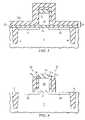
- Shallow trench isolation (STI) regions 4are formed in substrate 2 to isolate device regions. As is known in the art, STI regions 4 may be formed by etching recesses in substrate 2 , and then filling the recesses with dielectric materials.
- a gate stack 12which comprises a gate dielectric 14 , a gate electrode 16 and a hard mask 18 , is formed on substrate 2 .
- Gate dielectric 14includes commonly used dielectric materials such as oxides, nitrides, oxynitrides, oxycarbide, and combinations thereof.
- Gate electrode 16may include doped polysilicon, metals, metal silicides, metal nitrides, and combinations thereof.
- Hard mask 18may comprise silicon nitride or other materials such as oxides, oxynitrides, and silicon carbide.
- gate dielectric 14 , gate electrode 16 and hard mask 18may be formed by depositing stacked layers including a gate electrode layer on a gate dielectric layer, and a mask layer on the gate electrode layer, and then patterning the stacked layers.
- An optional pre-amorphized implantationmay be performed to reduce the dopant channeling effect and enhance dopant activation.
- silicon, germanium and/or carbonare implanted.
- inert gasessuch as neon, argon, krypton, xenon, and radon, are used.
- the pre-amorphized implantationprevents subsequently doped impurities from channeling through spaces between the crystal lattice structure and reaching depths greater than desired.
- LDD regions 20are then formed, preferably by implanting a p-type impurity, as is shown in FIG. 2 .
- Gate stack 12acts as a mask so that LDD regions 20 are substantially aligned with the edges of the respective gate stack 12 .
- Halo/pocket regionsare also formed, preferably by implanting n-type impurities.
- gate spacer layer 22is formed.
- gate spacer layer 22includes a liner oxide layer 22 1 and an overlying silicon nitride layer 22 2 .
- gate spacer layer 22includes one or more layers, each comprising oxide, silicon nitride, silicon oxynitride (SiON) and/or other dielectric materials, and may be formed using commonly used techniques, such as plasma enhanced chemical vapor deposition (PECVD), low-pressure chemical vapor deposition (LPCVD), sub-atmospheric chemical vapor deposition (SACVD), and the like.
- PECVDplasma enhanced chemical vapor deposition
- LPCVDlow-pressure chemical vapor deposition
- SACVDsub-atmospheric chemical vapor deposition
- FIG. 4illustrates the patterning of gate spacer layer 22 to form gate spacers 24 , wherein the patterning may be performed by either wet etching or dry etching. Horizontal portions of gate spacer layer 22 are removed, and the remaining portions of liner oxide layer 22 1 and silicon nitride layer 22 2 form liner oxide portions 24 1 and silicon nitride portions 24 2 , respectively.
- FIG. 4illustrates the formation of disposable spacers 26 .
- disposable spacers 26may be formed by blanket depositing a liner oxide layer, forming a silicon nitride layer on the liner oxide layer, and removing horizontal portions of the liner oxide layer and the silicon nitride layer. Accordingly, the preferred disposable spacers 26 include silicon nitride portions 26 2 on liner oxide portions 26 1 . Alternatively, disposable spacers 26 may include other materials having different etching characteristics from the underlying spacers 24 .
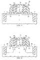
- recesses 28are formed along the edges of disposable spacers 26 , preferably by etching isotropically or anisotropically.
- the depth of recesses 28is preferably greater than the depth of the channel region of the resulting metal-oxide-semiconductor (MOS) device.
- MOSmetal-oxide-semiconductor
- disposable spacers 26are removed.
- the silicon nitride portions of disposable spacers 26are removed by etching in phosphoric acid, and the liner oxide portions of disposable spacers 26 are stripped using diluted hydrofluoric acid.
- a second recessing processis then performed to form recesses 30 .
- recesses 28are deepened, and are likely to expand toward a region underlying gate electrode 16 . Due to the removal of disposable spacers 26 , recesses 30 , which are closer to the channel region of the resulting MOS device, are formed.
- Recesses 30are preferably substantially shallower than recesses 28 . Recesses 30 may extend under spacers 24 , while recesses 28 may or may not extend under spacers 24 , depending on the thickness of disposable spacers 26 .
- depth T 1 of recesses 30is preferably between about 50 ⁇ and about 200 ⁇ . More preferably, depth T 1 of recesses 30 is less than about 70 percent of depth T 2 of recesses 28 . More preferably, depth T 1 is between about 20 percent and about 70 percent of depth T 2 . In 90 nm technology, the combined depth of recesses 28 and 30 is between about 500 ⁇ and about 1000 ⁇ , and more preferably between about 700 ⁇ and 900 ⁇ .
- a lateral distance DI between the edges of recesses 28 to the respective edges of gate electrode 16is preferably between about 10 nm and about 30 nm.
- a lateral distance D 2 between edges of recesses 30 to the respective edges of gate electrode 16is preferably between about 3 nm and about 15 nm.
- Recesses 30extend more toward the channel region than recesses 28 .
- the inner edges of recesses 28 and 30preferably have a lateral difference D 3 of about 5 nm and about 15 nm. It should be appreciated, however, that the dimensions recited throughout the description are merely examples, and the dimensions may scale accordingly with the scaling of technologies used for the formation of integrated circuits.
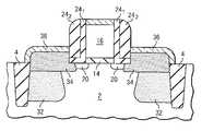
- FIG. 8illustrates the formation of epitaxy regions, often referred to as SiGe stressors or SiGe regions.
- SiGe regions 32are first epitaxially grown in recesses 28 by selective epitaxial growth (SEG).
- SiGe regions 32preferably have a lattice spacing greater than the lattice spacing of substrate 2 .
- SiGe regions 32are formed using PECVD in a chamber, in which the pressure is preferably between about 10 torr and about 200 torr.
- the preferred temperatureis between about 400° C. and about 1000° C.
- the precursorsinclude Si-containing gases and Ge-containing gases, such as SiH 4 and GeH 4 , respectively, and the partial pressures of the Si-containing gases and Ge-containing gases are adjusted to modify the atomic ratio of germanium to silicon.
- the resulting SiGe regions 32include between about 15 atomic percent and about 25 atomic percent germanium. It has been found that in such a structure, SiGe is typically epitaxially grown in recesses 28 first, while very little SiGe is formed in recesses 30 (particularly sidewalls of recesses 30 ) before recesses 28 are filled. In the preferred embodiment, the formation of SiGe regions 32 is stopped when their top surfaces are substantially level with bottom surfaces of recesses 30 .
- p-type impuritiessuch as boron
- the p-type impurity concentrationis between about 5 ⁇ 10 20 /cm 3 and about 1 ⁇ 10 21 /cm 3 , or between about one atomic percent to about two atomic percent, wherein the recited atomic percentage is the atomic percentage of p-type impurity atoms to atoms of silicon, germanium and the p-type impurity atoms.
- process conditions for the epitaxial processare changed to form SiGe regions 34 on SiGe regions 32 , wherein more germanium is introduced than in the formation of SiGe regions 32 .
- the formation of SiGe regions 34is performed in-situ with the formation of SiGe regions 32 .
- the partial pressures, hence flow rates, of the Ge-containing gases such as GeH 4is increased to increase the germanium concentration in SiGe regions 34 .
- the resulting SiGe regions 34have a higher germanium concentration, which is preferably between about 25 atomic percent and about 40 atomic percent, than SiGe regions 32 . More preferably, the atomic percentage of germanium in SiGe regions 34 and the atomic percentages of germanium in SiGe regions 32 have a difference of greater than about 5 atomic percent.
- the epitaxial process for forming SiGe regions 34is also preferably accompanied by the doping of p-type impurities, such as boron, wherein the p-type impurity concentration in SiGe regions 34 is preferably less than the p-type impurity concentration in SiGe regions 32 .
- the p-type impurity concentration in SiGe regions 34is between about 1 ⁇ 10 19 /cm 3 and about 5 ⁇ 10 20 /cm 3 , or between about 0.02 atomic percent to about one atomic percent.
- the p-type impurity concentration in SiGe regions 32is less than about 10 percent, or even about 1 percent, of the atomic percentage in SiGe regions 34 .
- SiGe regions 32 and 34may be doped with different p-type impurities.
- SiGe regions 34are doped with boron while SiGe regions 32 are doped with indium.
- the doped SiGe regions 32 and 34form at least portions of the source/drain regions of the resulting p-type MOS (PMOS) device.
- an implantation of p-type impuritiesmay further be performed for the formation of source/drain regions optionally.
- FIG. 10illustrates the formation of germano-silicide regions 36 .
- germano-silicide regions 36are also referred to as silicide regions 36 .
- germano-silicide regions 36are preferably formed by blanket depositing a thin layer of metal (not shown), such as nickel, platinum, palladium, vanadium, titanium, cobalt, tantalum, ytterbium, zirconium, and combinations thereof. The substrate is then heated, which causes silicon and germanium to react with the metal where contacted. After the reaction, a layer of metal silicide and/or metal germano-silicide is formed between silicon/germanium and metal. The un-reacted metal is selectively removed through the use of an etchant that attacks metal but does not attack silicide and germano-silicide.
- NMOSn-type MOS
- the NMOS embodimentspreferably include a first SiC stressor on a second SiC stressor, and the first SiC stressor is closer to the channel region than the second SiC stressor.
- the first and the second SiC stressorsare preferably doped with n-type impurities, such as phosphorus and arsenic, which also have the effect of relaxing the stress applied by the first and the second SiC stressors.
- the first SiC stressorpreferably has a lower n-type impurity concentration than the second SiC stressor, and the respective impurity concentrations in the first and the second SiC stressors may have a similar ratio as a ratio of an impurity concentration in SiGe regions 34 to an impurity concentration in SiGe regions 32 .
- SiGe regions 34which are on opposite sides of the channel region of the MOS device, have a high germanium atomic percentage, and thus apply a high stress to the channel region of the respective MOS device.
- the extension of SiGe regions 34 closer to the channel regionfurther increases the stress.
- impurity concentration in SiGe regions 34which extends into LDD regions 20 , is low. Therefore, less impurity is diffused into channel region, and the adverse effects to the short channel characteristics are reduced.
Landscapes
- Insulated Gate Type Field-Effect Transistor (AREA)
Abstract
Description
- This invention relates generally to integrated circuits, and more particularly to structure and formation methods of metal-oxide-semiconductor (MOS) devices with stressors.
- Reductions in the size and inherent features of semiconductor devices (e.g., a metal-oxide semiconductor field-effect transistor) have enabled continued improvement in speed, performance, density, and cost per unit function of integrated circuits over the past few decades. In accordance with a design of the transistor and one of the inherent characteristics thereof, modulating the length of a channel region underlying a gate between a source and drain of the transistor alters a resistance associated with the channel region, thereby affecting the performance of the transistor. More specifically, shortening the length of the channel region reduces a source-to-drain resistance of the transistor, which, assuming other parameters are maintained relatively constant, may allow an increase in current flow between the source and drain when a sufficient voltage is applied to the gate of the transistor.
- To further enhance the performance of metal-oxide-semiconductor (MOS) devices, stress may be introduced in the channel region of a MOS transistor to improve carrier mobility. Generally, it is desirable to induce a tensile stress in the channel region of an n-type MOS (NMOS) device in a source-to-drain direction and to induce a compressive stress in the channel region of a p-type MOS (PMOS) device in a source-to-drain direction.
- A commonly used method for applying compressive stress to the channel regions of PMOS devices is to grow silicon-germanium (SiGe) stressors in source and drain regions. Such a method typically includes the steps of forming a gate stack on a semiconductor substrate; forming spacers on sidewalls of the gate stack; forming recesses in the silicon substrate along the gate spacers; epitaxially growing SiGe stressors in the recesses, and then annealing. Since SiGe has a greater lattice constant than silicon has, it expands after annealing and applies a compressive stress to the channel region, which is located between a source SiGe stressor and a drain SiGe stressor.
- The conventional stressor formation processes suffer drawbacks, however. Boron is a commonly used p-type impurity for source/drain regions and lightly doped source/drain regions. To reduce sheet resistance, it is preferred that the boron concentration is high. However, the addition of boron has the effect of reducing lattice constant, and thus with a higher boron concentration, the strain introduced by SiGe stressors becomes more relaxed. In addition, a high boron concentration results in more boron to be diffused into channel regions, and the short channel characteristics are adversely affected.
- Therefore, new methods for preserving a high boron concentration in MOS devices without incurring the drawbacks are needed.
- In accordance with one aspect of the present invention, a semiconductor includes a semiconductor substrate, a gate stack on the semiconductor substrate, and a stressor having at least a portion in the semiconductor substrate and adjacent to the gate stack. The stressor includes a first stressor region and a second stressor region on the first stressor region, wherein the second stressor region extends laterally closer to a channel region underlying the gate stack than the first stressor region.
- In accordance with another aspect of the present invention, a semiconductor structure includes a semiconductor substrate, a gate stack on the semiconductor substrate, a gate spacer on a sidewall of the gate stack, a shallow stressor having at least a portion in the semiconductor substrate and adjacent to the gate stack wherein the shallow stressor extends under the gate spacer, and a deep stressor underlying and adjoining the shallow stressor, wherein the deep stressor is substantially free from under the gate spacer.
- In accordance with yet another aspect of the present invention, a semiconductor structure includes a semiconductor substrate, a gate stack on the semiconductor substrate, and a SiGe stressor having at least a portion in the semiconductor substrate and adjacent to the gate stack. The SiGe stressor includes a first SiGe region having a first atomic percentage of germanium to germanium and silicon, and a second SiGe region on the first SiGe region and having a second atomic percentage of germanium to germanium and silicon, wherein the second atomic percentage is greater than the first atomic percentage, and wherein the second SiGe region is laterally closer to a channel region than the first SiGe region.
- In accordance with yet another aspect of the present invention, a method for forming a semiconductor structure includes providing a semiconductor substrate, forming a gate stack on the semiconductor substrate, and forming a stressor having at least a portion in the semiconductor substrate and adjacent to the gate stack. The step of forming the stressor includes forming a first stressor region, and forming a second stressor region on the first stressor region, wherein the second stressor region extends laterally closer to a channel region underlying the gate stack than the first stressor region.
- In accordance with yet another aspect of the present invention, a method of forming a semiconductor structure includes providing a semiconductor substrate, forming a gate stack on the semiconductor substrate, forming a gate spacer on a sidewall of the gate stack, forming a disposable spacer on a sidewall of the gate spacer, forming a first recess along a sidewall of the disposable spacer, removing the disposable spacer, forming a second recess along the sidewall of the gate spacer wherein the second recess is substantially shallower than the first recess, forming a first SiGe region in the first recess, and forming a second SiGe region in the second recess.
- The advantageous features of the present invention includes increased stress applied to channel regions of MOS devices due to shorter distances between stressors and the channel regions, and reduced impurity diffusion into the channel regions due to low impurity concentrations in regions close to the channel regions.
- For a more complete understanding of the present invention, and the advantages thereof, reference is now made to the following descriptions taken in conjunction with the accompanying drawings, in which:
FIGS. 1 through 10 are cross-sectional views of intermediate stages in the manufacturing of a preferred embodiment, wherein SiGe stressors comprise two regions having different compositions.- The making and using of the presently preferred embodiments are discussed in detail below. It should be appreciated, however, that the present invention provides many applicable inventive concepts that can be embodied in a wide variety of specific contexts. The specific embodiments discussed are merely illustrative of specific ways to make and use the invention, and do not limit the scope of the invention.
- A novel method for improving the formation of stressors is illustrated in
FIGS. 1 through 10 . Throughout the various views and illustrative embodiments of the present invention, like reference numbers are used to designate like elements. - Referring to
FIG. 1 , asubstrate 2 is provided.Substrate 2 is preferably a bulk silicon substrate. Alternatively,substrate 2 comprises bulk silicon-germanium (SiGe) (with a low germanium concentration) or other semiconductor materials.Substrate 2 may also have a composite structure such as silicon-on-insulator (SOI). Shallow trench isolation (STI)regions 4 are formed insubstrate 2 to isolate device regions. As is known in the art,STI regions 4 may be formed by etching recesses insubstrate 2, and then filling the recesses with dielectric materials. - Referring to
FIG. 2 , agate stack 12, which comprises a gate dielectric14, agate electrode 16 and ahard mask 18, is formed onsubstrate 2. Gate dielectric14 includes commonly used dielectric materials such as oxides, nitrides, oxynitrides, oxycarbide, and combinations thereof.Gate electrode 16 may include doped polysilicon, metals, metal silicides, metal nitrides, and combinations thereof.Hard mask 18 may comprise silicon nitride or other materials such as oxides, oxynitrides, and silicon carbide. As is known in the art, gate dielectric14,gate electrode 16 andhard mask 18 may be formed by depositing stacked layers including a gate electrode layer on a gate dielectric layer, and a mask layer on the gate electrode layer, and then patterning the stacked layers. - An optional pre-amorphized implantation (PAI) may be performed to reduce the dopant channeling effect and enhance dopant activation. In the preferred embodiment, silicon, germanium and/or carbon are implanted. In other embodiments, inert gases, such as neon, argon, krypton, xenon, and radon, are used. The pre-amorphized implantation prevents subsequently doped impurities from channeling through spaces between the crystal lattice structure and reaching depths greater than desired.
- Lightly doped source/drain (LDD)
regions 20 are then formed, preferably by implanting a p-type impurity, as is shown inFIG. 2 .Gate stack 12 acts as a mask so thatLDD regions 20 are substantially aligned with the edges of therespective gate stack 12. Halo/pocket regions (not shown) are also formed, preferably by implanting n-type impurities. - Referring to
FIG. 3 , agate spacer layer 22 is formed. In the preferred embodiment,gate spacer layer 22 includes aliner oxide layer 221and an overlyingsilicon nitride layer 222. In alternative embodiments,gate spacer layer 22 includes one or more layers, each comprising oxide, silicon nitride, silicon oxynitride (SiON) and/or other dielectric materials, and may be formed using commonly used techniques, such as plasma enhanced chemical vapor deposition (PECVD), low-pressure chemical vapor deposition (LPCVD), sub-atmospheric chemical vapor deposition (SACVD), and the like. FIG. 4 illustrates the patterning ofgate spacer layer 22 to formgate spacers 24, wherein the patterning may be performed by either wet etching or dry etching. Horizontal portions ofgate spacer layer 22 are removed, and the remaining portions ofliner oxide layer 221andsilicon nitride layer 222formliner oxide portions 241andsilicon nitride portions 242, respectively.FIG. 4 illustrates the formation ofdisposable spacers 26. Similar tospacers 24,disposable spacers 26 may be formed by blanket depositing a liner oxide layer, forming a silicon nitride layer on the liner oxide layer, and removing horizontal portions of the liner oxide layer and the silicon nitride layer. Accordingly, the preferreddisposable spacers 26 includesilicon nitride portions 262onliner oxide portions 261. Alternatively,disposable spacers 26 may include other materials having different etching characteristics from theunderlying spacers 24.- Referring to
FIG. 6 ,recesses 28 are formed along the edges ofdisposable spacers 26, preferably by etching isotropically or anisotropically. The depth ofrecesses 28 is preferably greater than the depth of the channel region of the resulting metal-oxide-semiconductor (MOS) device. - In
FIG. 7 ,disposable spacers 26 are removed. In an exemplary embodiment, the silicon nitride portions ofdisposable spacers 26 are removed by etching in phosphoric acid, and the liner oxide portions ofdisposable spacers 26 are stripped using diluted hydrofluoric acid. A second recessing process is then performed to form recesses30. During the second recessing process, recesses28 are deepened, and are likely to expand toward a region underlyinggate electrode 16. Due to the removal ofdisposable spacers 26, recesses30, which are closer to the channel region of the resulting MOS device, are formed.Recesses 30 are preferably substantially shallower than recesses28.Recesses 30 may extend underspacers 24, whilerecesses 28 may or may not extend underspacers 24, depending on the thickness ofdisposable spacers 26. - In an exemplary embodiment, depth T1 of
recesses 30 is preferably between about 50 Å and about 200 Å. More preferably, depth T1 ofrecesses 30 is less than about 70 percent of depth T2 ofrecesses 28. More preferably, depth T1 is between about 20 percent and about 70 percent of depth T2. In 90 nm technology, the combined depth ofrecesses - A lateral distance DI between the edges of
recesses 28 to the respective edges ofgate electrode 16 is preferably between about 10 nm and about 30 nm. A lateral distance D2 between edges ofrecesses 30 to the respective edges ofgate electrode 16 is preferably between about 3 nm and about 15 nm.Recesses 30 extend more toward the channel region than recesses28. In an exemplary embodiment, the inner edges ofrecesses FIG. 8 illustrates the formation of epitaxy regions, often referred to as SiGe stressors or SiGe regions.SiGe regions 32 are first epitaxially grown inrecesses 28 by selective epitaxial growth (SEG).SiGe regions 32 preferably have a lattice spacing greater than the lattice spacing ofsubstrate 2. In an exemplary embodiment,SiGe regions 32 are formed using PECVD in a chamber, in which the pressure is preferably between about 10 torr and about 200 torr. The preferred temperature is between about 400° C. and about 1000° C. The precursors include Si-containing gases and Ge-containing gases, such as SiH4and GeH4, respectively, and the partial pressures of the Si-containing gases and Ge-containing gases are adjusted to modify the atomic ratio of germanium to silicon. In the preferred embodiment, the resultingSiGe regions 32 include between about 15 atomic percent and about 25 atomic percent germanium. It has been found that in such a structure, SiGe is typically epitaxially grown inrecesses 28 first, while very little SiGe is formed in recesses30 (particularly sidewalls of recesses30) beforerecesses 28 are filled. In the preferred embodiment, the formation ofSiGe regions 32 is stopped when their top surfaces are substantially level with bottom surfaces ofrecesses 30.- During the epitaxial process for forming
SiGe regions 32, p-type impurities, such as boron, are doped. Preferably, the p-type impurity concentration is between about 5×10²⁰/cm3and about 1×10²¹/cm3, or between about one atomic percent to about two atomic percent, wherein the recited atomic percentage is the atomic percentage of p-type impurity atoms to atoms of silicon, germanium and the p-type impurity atoms. - Referring to
FIG. 9 , process conditions for the epitaxial process are changed to formSiGe regions 34 onSiGe regions 32, wherein more germanium is introduced than in the formation ofSiGe regions 32. Preferably, the formation ofSiGe regions 34 is performed in-situ with the formation ofSiGe regions 32. In an exemplary embodiment, the partial pressures, hence flow rates, of the Ge-containing gases such as GeH4is increased to increase the germanium concentration inSiGe regions 34. The resultingSiGe regions 34 have a higher germanium concentration, which is preferably between about 25 atomic percent and about 40 atomic percent, thanSiGe regions 32. More preferably, the atomic percentage of germanium inSiGe regions 34 and the atomic percentages of germanium inSiGe regions 32 have a difference of greater than about 5 atomic percent. - The epitaxial process for forming
SiGe regions 34 is also preferably accompanied by the doping of p-type impurities, such as boron, wherein the p-type impurity concentration inSiGe regions 34 is preferably less than the p-type impurity concentration inSiGe regions 32. In an exemplary embodiment, the p-type impurity concentration inSiGe regions 34 is between about 1×10¹⁹/cm3and about 5×10²⁰/cm3, or between about 0.02 atomic percent to about one atomic percent. Preferably, the p-type impurity concentration inSiGe regions 32 is less than about 10 percent, or even about 1 percent, of the atomic percentage inSiGe regions 34.SiGe regions SiGe regions 34 are doped with boron whileSiGe regions 32 are doped with indium. Thedoped SiGe regions SiGe regions 34, an implantation of p-type impurities may further be performed for the formation of source/drain regions optionally. FIG. 10 illustrates the formation of germano-silicide regions 36. Throughout the description, germano-silicide regions 36 are also referred to assilicide regions 36. As is known in the art, germano-silicide regions 36 are preferably formed by blanket depositing a thin layer of metal (not shown), such as nickel, platinum, palladium, vanadium, titanium, cobalt, tantalum, ytterbium, zirconium, and combinations thereof. The substrate is then heated, which causes silicon and germanium to react with the metal where contacted. After the reaction, a layer of metal silicide and/or metal germano-silicide is formed between silicon/germanium and metal. The un-reacted metal is selectively removed through the use of an etchant that attacks metal but does not attack silicide and germano-silicide.- The concept of the present invention can also be applied to the formation of n-type MOS (NMOS) devices, which preferably have SiC stressors. Similar to the embodiment shown in
FIG. 10 , the NMOS embodiments preferably include a first SiC stressor on a second SiC stressor, and the first SiC stressor is closer to the channel region than the second SiC stressor. The first and the second SiC stressors are preferably doped with n-type impurities, such as phosphorus and arsenic, which also have the effect of relaxing the stress applied by the first and the second SiC stressors. In addition, The first SiC stressor preferably has a lower n-type impurity concentration than the second SiC stressor, and the respective impurity concentrations in the first and the second SiC stressors may have a similar ratio as a ratio of an impurity concentration inSiGe regions 34 to an impurity concentration inSiGe regions 32. - The preferred embodiments of the present invention have several advantageous features.
SiGe regions 34, which are on opposite sides of the channel region of the MOS device, have a high germanium atomic percentage, and thus apply a high stress to the channel region of the respective MOS device. The extension ofSiGe regions 34 closer to the channel region further increases the stress. On the other hand, impurity concentration inSiGe regions 34, which extends intoLDD regions 20, is low. Therefore, less impurity is diffused into channel region, and the adverse effects to the short channel characteristics are reduced. - Although the present invention and its advantages have been described in detail, it should be understood that various changes, substitutions and alterations can be made herein without departing from the spirit and scope of the invention as defined by the appended claims. Moreover, the scope of the present application is not intended to be limited to the particular embodiments of the process, machine, manufacture, and composition of matter, means, methods and steps described in the specification. As one of ordinary skill in the art will readily appreciate from the disclosure of the present invention, processes, machines, manufacture, compositions of matter, means, methods, or steps, presently existing or later to be developed, that perform substantially the same function or achieve substantially the same result as the corresponding embodiments described herein may be utilized according to the present invention. Accordingly, the appended claims are intended to include within their scope such processes, machines, manufacture, compositions of matter, means, methods, or steps.
Claims (30)
1. A semiconductor structure comprising:
a semiconductor substrate;
a gate stack on the semiconductor substrate; and
a stressor having at least a portion in the semiconductor substrate and adjacent to the gate stack, wherein the stressor comprises:
a first stressor region; and
a second stressor region on the first stressor region, wherein the second stressor region extends laterally closer to a channel region underlying the gate stack than the first stressor region.
2. The semiconductor structure ofclaim 1 , wherein the stressor comprises SiGe.
3. The semiconductor structure ofclaim 2 , wherein the first stressor region has a first atomic percentage of germanium to germanium and silicon, the second stressor region has a second atomic percentage of germanium to germanium and silicon, and the second atomic percentage is higher than the first atomic percentage.
4. The semiconductor structure ofclaim 1 , wherein the first stressor region has a first impurity concentration and the second stressor region has a second impurity concentration, and wherein the first impurity concentration is greater than the second impurity concentration.
5. The semiconductor structure ofclaim 1 , wherein the stressor comprises SiC.
6. The semiconductor structure ofclaim 1 , wherein the second stressor region is closer to the channel region than the first stressor region by greater than about 5 nm.
7. The semiconductor structure ofclaim 1 , wherein the first stressor region has a first thickness and the second stressor region has a second thickness, and wherein the second thickness is between about 20 and about 70 percent of the first thickness.
8. A semiconductor structure comprising:
a semiconductor substrate;
a gate stack on the semiconductor substrate;
a gate spacer on a sidewall of the gate stack;
a shallow stressor having at least a portion in the semiconductor substrate and adjacent to the gate stack, wherein the shallow stressor extends under the gate spacer; and
a deep stressor underlying and adjoining the shallow stressor, wherein the deep stressor is substantially free from under the gate spacer.
9. The semiconductor structure ofclaim 8 , wherein the deep stressor has a first atomic percentage of germanium to germanium and silicon, and the shallower stressor has a second atomic percentage of germanium to germanium and silicon, and wherein the first atomic percentage is less than the second atomic percentage.
10. The semiconductor structure ofclaim 8 , wherein the deep stressor has a first impurity concentration, and the shallower stressor has a second impurity concentration, and wherein the first impurity concentration is greater than the second impurity concentration.
11. The semiconductor structure ofclaim 8 , wherein the shallow stressor extends toward a channel region underlying the gate stack than the deep stressor by a distance of greater than about 5 nm.
12. A semiconductor structure comprising:
a semiconductor substrate;
a gate stack on the semiconductor substrate; and
a SiGe stressor having at least a portion in the semiconductor substrate and adjacent to the gate stack, wherein the SiGe stressor comprises:
a first SiGe region having a first atomic percentage of germanium to germanium and silicon; and
a second SiGe region on the first SiGe region and having a second atomic percentage of germanium to germanium and silicon, wherein the second atomic percentage is greater than the first atomic percentage, and wherein the second SiGe region is laterally closer to a channel region than the first SiGe region.
13. The semiconductor structure ofclaim 12 , wherein the second atomic percentage is between about 25 percent and about 40 percent, and wherein the first atomic percentage is between about 15 percent and about 25 percent.
14. The semiconductor structure ofclaim 12 , wherein the first atomic percentage is less than about the second atomic percentage by greater than about 5 atomic percent.
15. The semiconductor structure ofclaim 12 , wherein the first SiGe stressor has a first p-type impurity concentration and the second SiGe stressor has a second p-type impurity concentration less than the first p-type impurity concentration.
16. The semiconductor structure ofclaim 15 , wherein the first p-type impurity concentration is between about 5×10²⁰/cm3and about 1×10²¹/cm3, and the second p-type impurity concentration is between about 1×10¹⁹/cm3and about 5×10²⁰/cm3.
17. The semiconductor structure ofclaim 15 , wherein second p-type impurity concentration is less than about 10 percent of the first p-type impurity concentration.
18. A method for forming a semiconductor structure, the method comprising:
providing a semiconductor substrate;
forming a gate stack on the semiconductor substrate; and
forming a stressor having at least a portion in the semiconductor substrate and adjacent to the gate stack, wherein the step of forming the stressor comprises:
forming a first stressor region; and
forming a second stressor region on the first stressor region, wherein the second stressor region extends laterally closer to a channel region underlying the gate stack than the first stressor region.
19. The method ofclaim 18 , wherein the step of forming the stressor comprises:
recessing the semiconductor substrate to form a first recess;
recessing the semiconductor substrate to form a second recess, wherein the second recess is closer to the gate stack than the first stress;
epitaxially growing the first stressor region in the first recess; and
epitaxially growing the second stressor region in the second recess.
20. The method ofclaim 19 , wherein the steps of forming the first and the second recesses comprise:
forming a gate spacer on a sidewall of the gate stack;
forming a disposable spacer on a sidewall of the gate spacer;
forming the first recess along a sidewall of the disposable spacer;
removing the disposable spacer; and
forming the second recess along the sidewall of the gate spacer, wherein the second recess is substantially shallower than the first recess.
21. The method ofclaim 18 , wherein the first stressor region has a first atomic percentage of germanium to germanium and silicon, the second stressor region has a second atomic percentage of germanium to germanium and silicon, and the second atomic percentage is higher than the first atomic percentage.
22. The method ofclaim 18 , wherein the step of forming the first and the second stressors comprise forming the first stressor using a first flow rate of a Ge-containing precursor, and forming the second stressor using a second flow rate of the Ge-containing precursor, wherein the second flow rate is greater than the first flow rate.
23. The method ofclaim 18 , wherein the first atomic percentage is between about 15 percent and about 25 percent, and wherein the second atomic percentage is between about 25 percent and about 40 percent.
24. The method ofclaim 18 , wherein the first stressor region has a first impurity concentration and the second stressor region has a second impurity concentration, and wherein the second impurity concentration is less than the first impurity concentration.
25. A method of forming a semiconductor structure, the method comprising:
providing a semiconductor substrate;
forming a gate stack on the semiconductor substrate;
forming a gate spacer on a sidewall of the gate stack;
forming a disposable spacer on a sidewall of the gate spacer;
forming a first recess along a sidewall of the disposable spacer;
removing the disposable spacer;
forming a second recess along the sidewall of the gate spacer, wherein the second recess is substantially shallower than the first recess;
forming a first SiGe region in the first recess; and
forming a second SiGe region in the second recess.
26. The method ofclaim 25 , wherein the second SiGe region has a higher germanium concentration of germanium to germanium and silicon than the first SiGe region.
27. The method ofclaim 26 , wherein the step of forming the second SiGe region is performed in a formation environment comprising a higher GeH4flow rate than in the step of forming the first SiGe region.
28. The method ofclaim 25 further comprising doping p-type impurities during the steps of forming the first and the second SiGe regions, wherein the first SiGe region has a first impurity concentration higher than a second p-type impurity concentration in the first SiGe region.
29. The method ofclaim 28 further comprising implanting a p-type impurity into the first and the second SiGe regions after the steps of forming the first and the second SiGe regions.
30. The method ofclaim 28 , wherein the first p-type impurity concentration is between about 5×10²⁰/cm3and about 1×10²¹/cm3, and the second p-type impurity concentration is between about 1×10⁹/cm3and about 5×10²⁰/cm3.
Priority Applications (2)
| Application Number | Priority Date | Filing Date | Title |
|---|---|---|---|
| US11/633,855US7750338B2 (en) | 2006-12-05 | 2006-12-05 | Dual-SiGe epitaxy for MOS devices |
| US12/790,304US9466716B2 (en) | 2006-12-05 | 2010-05-28 | Dual-SiGe epitaxy for MOS devices |
Applications Claiming Priority (1)
| Application Number | Priority Date | Filing Date | Title |
|---|---|---|---|
| US11/633,855US7750338B2 (en) | 2006-12-05 | 2006-12-05 | Dual-SiGe epitaxy for MOS devices |
Related Child Applications (1)
| Application Number | Title | Priority Date | Filing Date |
|---|---|---|---|
| US12/790,304DivisionUS9466716B2 (en) | 2006-12-05 | 2010-05-28 | Dual-SiGe epitaxy for MOS devices |
Publications (2)
| Publication Number | Publication Date |
|---|---|
| US20080128746A1true US20080128746A1 (en) | 2008-06-05 |
| US7750338B2 US7750338B2 (en) | 2010-07-06 |
Family
ID=39474690
Family Applications (2)
| Application Number | Title | Priority Date | Filing Date |
|---|---|---|---|
| US11/633,855Active2027-02-21US7750338B2 (en) | 2006-12-05 | 2006-12-05 | Dual-SiGe epitaxy for MOS devices |
| US12/790,304Expired - Fee RelatedUS9466716B2 (en) | 2006-12-05 | 2010-05-28 | Dual-SiGe epitaxy for MOS devices |
Family Applications After (1)
| Application Number | Title | Priority Date | Filing Date |
|---|---|---|---|
| US12/790,304Expired - Fee RelatedUS9466716B2 (en) | 2006-12-05 | 2010-05-28 | Dual-SiGe epitaxy for MOS devices |
Country Status (1)
| Country | Link |
|---|---|
| US (2) | US7750338B2 (en) |
Cited By (63)
| Publication number | Priority date | Publication date | Assignee | Title |
|---|---|---|---|---|
| US20070228417A1 (en)* | 2006-04-03 | 2007-10-04 | Kabushiki Kaisha Toshiba | Semiconductor device and method of fabricating the same |
| US20080220594A1 (en)* | 2007-03-05 | 2008-09-11 | Commissariat A L' Energie Atomique | Fabrication method of a mixed substrate and use of the substrate for producing circuits |
| US20090114956A1 (en)* | 2007-11-01 | 2009-05-07 | Fujitsu Microelectronics Limited | Semiconductor device and manufacturing method thereof |
| US20090280627A1 (en)* | 2008-05-12 | 2009-11-12 | Advanced Micro Devices, Inc. | Method of forming stepped recesses for embedded strain elements in a semiconductor device |
| US20100093147A1 (en)* | 2008-10-14 | 2010-04-15 | Chin-I Liao | Method for forming a semiconductor device |
| US20100105184A1 (en)* | 2008-10-27 | 2010-04-29 | Fujitsu Microelectronics Limited | Method of manufacturing a semiconductor device |
| US20100164020A1 (en)* | 2008-12-31 | 2010-07-01 | Stephan Kronholz | Transistor with an embedded strain-inducing material having a gradually shaped configuration |
| US20100187578A1 (en)* | 2009-01-26 | 2010-07-29 | International Business Machines Corporation | Stress enhanced transistor devices and methods of making |
| US20100187579A1 (en)* | 2009-01-26 | 2010-07-29 | International Business Machines Corporation | Transistor devices and methods of making |
| US20100301350A1 (en)* | 2008-01-25 | 2010-12-02 | Fujitsu Semiconductor Limited | Semiconductor device and manufacturing method thereof |
| US20110024801A1 (en)* | 2009-07-30 | 2011-02-03 | Taiwan Semiconductor Manufacturing Company, Ltd. | Transistors having a composite strain structure, integrated circuits, and fabrication methods thereof |
| US7943471B1 (en)* | 2006-05-15 | 2011-05-17 | Globalfoundries Inc. | Diode with asymmetric silicon germanium anode |
| US20110136311A1 (en)* | 2008-03-10 | 2011-06-09 | Dong-Suk Shin | Semiconductor device having a locally buried insulation layer and method of manufacturing the semiconductor device |
| CN102148236A (en)* | 2010-02-09 | 2011-08-10 | 台湾积体电路制造股份有限公司 | Semiconductor element and its manufacturing method |
| WO2011131053A1 (en)* | 2010-04-21 | 2011-10-27 | 中国科学院微电子研究所 | Source and drain regions, contact holes and fabrication methods thereof |
| US8324059B2 (en) | 2011-04-25 | 2012-12-04 | United Microelectronics Corp. | Method of fabricating a semiconductor structure |
| US20130001660A1 (en)* | 2007-10-17 | 2013-01-03 | International Business Machines Corporation | Planar field effect transistor structure and method |
| US8405160B2 (en) | 2010-05-26 | 2013-03-26 | Taiwan Semiconductor Manufacturing Company, Ltd. | Multi-strained source/drain structures |
| US8426284B2 (en) | 2011-05-11 | 2013-04-23 | United Microelectronics Corp. | Manufacturing method for semiconductor structure |
| US8431460B2 (en) | 2011-05-27 | 2013-04-30 | United Microelectronics Corp. | Method for fabricating semiconductor device |
| US20130113027A1 (en)* | 2011-11-09 | 2013-05-09 | Wen-Tai Chiang | Metal Oxide Semiconductor Transistor and Manufacturing Method Thereof |
| US8445363B2 (en) | 2011-04-21 | 2013-05-21 | United Microelectronics Corp. | Method of fabricating an epitaxial layer |
| US20130149830A1 (en)* | 2011-12-07 | 2013-06-13 | Samsung Electronics Co., Ltd. | Methods of forming field effect transistors having silicon-germanium source/drain regions therein |
| US8466502B2 (en) | 2011-03-24 | 2013-06-18 | United Microelectronics Corp. | Metal-gate CMOS device |
| US8476169B2 (en) | 2011-10-17 | 2013-07-02 | United Microelectronics Corp. | Method of making strained silicon channel semiconductor structure |
| US8481391B2 (en) | 2011-05-18 | 2013-07-09 | United Microelectronics Corp. | Process for manufacturing stress-providing structure and semiconductor device with such stress-providing structure |
| US20130210207A1 (en)* | 2009-11-30 | 2013-08-15 | Fujitsu Semiconductor Limited | Fabrication method of semiconductor device and fabrication method of dynamic threshold transistor |
| US8575043B2 (en) | 2011-07-26 | 2013-11-05 | United Microelectronics Corp. | Semiconductor device and manufacturing method thereof |
| US20130295741A1 (en)* | 2007-06-27 | 2013-11-07 | Sony Corporation | Semiconductor device and method for manufacturing semiconductor device |
| US8647953B2 (en) | 2011-11-17 | 2014-02-11 | United Microelectronics Corp. | Method for fabricating first and second epitaxial cap layers |
| US8647941B2 (en) | 2011-08-17 | 2014-02-11 | United Microelectronics Corp. | Method of forming semiconductor device |
| US8664069B2 (en) | 2012-04-05 | 2014-03-04 | United Microelectronics Corp. | Semiconductor structure and process thereof |
| US8674433B2 (en) | 2011-08-24 | 2014-03-18 | United Microelectronics Corp. | Semiconductor process |
| US8691659B2 (en) | 2011-10-26 | 2014-04-08 | United Microelectronics Corp. | Method for forming void-free dielectric layer |
| US8709930B2 (en) | 2011-11-25 | 2014-04-29 | United Microelectronics Corp. | Semiconductor process |
| US8710632B2 (en) | 2012-09-07 | 2014-04-29 | United Microelectronics Corp. | Compound semiconductor epitaxial structure and method for fabricating the same |
| US8716750B2 (en) | 2011-07-25 | 2014-05-06 | United Microelectronics Corp. | Semiconductor device having epitaxial structures |
| US8753902B1 (en) | 2013-03-13 | 2014-06-17 | United Microelectronics Corp. | Method of controlling etching process for forming epitaxial structure |
| US8754448B2 (en) | 2011-11-01 | 2014-06-17 | United Microelectronics Corp. | Semiconductor device having epitaxial layer |
| US8765546B1 (en) | 2013-06-24 | 2014-07-01 | United Microelectronics Corp. | Method for fabricating fin-shaped field-effect transistor |
| CN103904116A (en)* | 2012-12-27 | 2014-07-02 | 美国博通公司 | Metal oxide semiconductor devices and fabrication methods |
| US8796695B2 (en) | 2012-06-22 | 2014-08-05 | United Microelectronics Corp. | Multi-gate field-effect transistor and process thereof |
| US8835243B2 (en) | 2012-05-04 | 2014-09-16 | United Microelectronics Corp. | Semiconductor process |
| US8853060B1 (en) | 2013-05-27 | 2014-10-07 | United Microelectronics Corp. | Epitaxial process |
| US20140302658A1 (en)* | 2012-04-27 | 2014-10-09 | International Business Machines Corporation | Transistor with improved sigma-shaped embedded stressor and method of formation |
| US8866230B2 (en) | 2012-04-26 | 2014-10-21 | United Microelectronics Corp. | Semiconductor devices |
| US8895396B1 (en) | 2013-07-11 | 2014-11-25 | United Microelectronics Corp. | Epitaxial Process of forming stress inducing epitaxial layers in source and drain regions of PMOS and NMOS structures |
| US8951876B2 (en) | 2012-06-20 | 2015-02-10 | United Microelectronics Corp. | Semiconductor device and manufacturing method thereof |
| US8981487B2 (en) | 2013-07-31 | 2015-03-17 | United Microelectronics Corp. | Fin-shaped field-effect transistor (FinFET) |
| US9034705B2 (en) | 2013-03-26 | 2015-05-19 | United Microelectronics Corp. | Method of forming semiconductor device |
| US9064893B2 (en) | 2013-05-13 | 2015-06-23 | United Microelectronics Corp. | Gradient dopant of strained substrate manufacturing method of semiconductor device |
| US9076652B2 (en) | 2013-05-27 | 2015-07-07 | United Microelectronics Corp. | Semiconductor process for modifying shape of recess |
| US9117925B2 (en) | 2013-01-31 | 2015-08-25 | United Microelectronics Corp. | Epitaxial process |
| US9136348B2 (en) | 2012-03-12 | 2015-09-15 | United Microelectronics Corp. | Semiconductor structure and fabrication method thereof |
| US20150342072A1 (en)* | 2012-06-04 | 2015-11-26 | Hitachi Metals, Ltd. | Seal ring and method for manufacturing seal ring |
| US9202914B2 (en) | 2012-03-14 | 2015-12-01 | United Microelectronics Corporation | Semiconductor device and method for fabricating the same |
| US20150357411A1 (en)* | 2014-03-19 | 2015-12-10 | International Business Machines Corporation | P-fet with strained silicon-germanium channel |
| US20150357436A1 (en)* | 2014-06-10 | 2015-12-10 | United Microelectronics Corp. | Semiconductor device and method for fabricating the same |
| US9583619B2 (en)* | 2015-02-13 | 2017-02-28 | Shanghai Huali Microelectronics Corporation | Semiconductor devices with shaped cavities for embedding germanium material and manufacturing processes thereof |
| CN106816379A (en)* | 2015-11-27 | 2017-06-09 | 联华电子股份有限公司 | Semiconductor element with epitaxial structure and manufacturing method thereof |
| US20170338327A1 (en)* | 2016-05-19 | 2017-11-23 | United Semiconductor (Xiamen) Co., Ltd. | Semiconductor device and manufacturing method thereof |
| US11004976B2 (en)* | 2010-09-07 | 2021-05-11 | Samsung Electronics Co., Ltd. | Semiconductor device including MOS transistor having silicided source/drain region and method of fabricating the same |
| US11335808B1 (en)* | 2020-12-07 | 2022-05-17 | Powerchip Semiconductor Manufacturing Corporation | Semiconductor device and manufacturing method thereof |
Families Citing this family (16)
| Publication number | Priority date | Publication date | Assignee | Title |
|---|---|---|---|---|
| US8362575B2 (en)* | 2009-09-29 | 2013-01-29 | Taiwan Semiconductor Manufacturing Company, Ltd. | Controlling the shape of source/drain regions in FinFETs |
| US8502316B2 (en)* | 2010-02-11 | 2013-08-06 | Taiwan Semiconductor Manufacturing Company, Ltd. | Self-aligned two-step STI formation through dummy poly removal |
| US8263451B2 (en)* | 2010-02-26 | 2012-09-11 | Taiwan Semiconductor Manufacturing Company, Ltd. | Epitaxy profile engineering for FinFETs |
| US8236660B2 (en) | 2010-04-21 | 2012-08-07 | International Business Machines Corporation | Monolayer dopant embedded stressor for advanced CMOS |
| US8299535B2 (en)* | 2010-06-25 | 2012-10-30 | International Business Machines Corporation | Delta monolayer dopants epitaxy for embedded source/drain silicide |
| DE102010064284B4 (en)* | 2010-12-28 | 2016-03-31 | GLOBALFOUNDRIES Dresden Module One Ltd. Liability Company & Co. KG | A method of making a transistor having an embedded sigma-shaped semiconductor alloy with increased uniformity |
| US8450194B2 (en)* | 2011-07-01 | 2013-05-28 | Varian Semiconductor Equipment Associates, Inc. | Method to modify the shape of a cavity using angled implantation |
| US9076817B2 (en)* | 2011-08-04 | 2015-07-07 | International Business Machines Corporation | Epitaxial extension CMOS transistor |
| US8921206B2 (en)* | 2011-11-30 | 2014-12-30 | United Microelectronics Corp. | Semiconductor process |
| JP5944266B2 (en)* | 2012-08-10 | 2016-07-05 | ルネサスエレクトロニクス株式会社 | Semiconductor device and manufacturing method thereof |
| EP2704199B1 (en)* | 2012-09-03 | 2020-01-01 | IMEC vzw | Method of manufacturing a semiconductor device |
| US9171762B2 (en) | 2012-11-01 | 2015-10-27 | Taiwan Semiconductor Manufacturing Company, Ltd. | Semiconductor device and fabrication method thereof |
| US10158000B2 (en)* | 2013-11-26 | 2018-12-18 | Taiwan Semiconductor Manufacturing Company Limited | Low-K dielectric sidewall spacer treatment |
| KR102230198B1 (en) | 2014-09-23 | 2021-03-19 | 삼성전자주식회사 | Semiconductor device and method for manufacturing the same |
| KR102259080B1 (en) | 2014-09-23 | 2021-06-03 | 삼성전자주식회사 | Semiconductor device and method of manufacturing the same |
| US10522555B2 (en) | 2018-04-04 | 2019-12-31 | Globalfoundries Inc. | Semiconductor devices including Si/Ge active regions with different Ge concentrations |
Citations (5)
| Publication number | Priority date | Publication date | Assignee | Title |
|---|---|---|---|---|
| US6492665B1 (en)* | 1998-07-28 | 2002-12-10 | Matsushita Electric Industrial Co., Ltd. | Semiconductor device |
| US20030052348A1 (en)* | 1999-11-15 | 2003-03-20 | Matsushita Electric Industrial Co., Ltd. | Semiconductor device |
| US20050082522A1 (en)* | 2003-07-25 | 2005-04-21 | Yi-Chun Huang | Strained channel transistor formation |
| US20070235802A1 (en)* | 2006-04-05 | 2007-10-11 | Chartered Semiconductor Manufacturing Ltd | Method to control source/drain stressor profiles for stress engineering |
| US7335959B2 (en)* | 2005-01-06 | 2008-02-26 | Intel Corporation | Device with stepped source/drain region profile |
Family Cites Families (4)
| Publication number | Priority date | Publication date | Assignee | Title |
|---|---|---|---|---|
| JP3544833B2 (en)* | 1997-09-18 | 2004-07-21 | 株式会社東芝 | Semiconductor device and manufacturing method thereof |
| US6812103B2 (en)* | 2002-06-20 | 2004-11-02 | Micron Technology, Inc. | Methods of fabricating a dielectric plug in MOSFETS to suppress short-channel effects |
| US7195985B2 (en)* | 2005-01-04 | 2007-03-27 | Intel Corporation | CMOS transistor junction regions formed by a CVD etching and deposition sequence |
| US7772071B2 (en)* | 2006-05-17 | 2010-08-10 | Chartered Semiconductor Manufacturing Ltd. | Strained channel transistor and method of fabrication thereof |
- 2006
- 2006-12-05USUS11/633,855patent/US7750338B2/enactiveActive
- 2010
- 2010-05-28USUS12/790,304patent/US9466716B2/ennot_activeExpired - Fee Related
Patent Citations (6)
| Publication number | Priority date | Publication date | Assignee | Title |
|---|---|---|---|---|
| US6492665B1 (en)* | 1998-07-28 | 2002-12-10 | Matsushita Electric Industrial Co., Ltd. | Semiconductor device |
| US20030052348A1 (en)* | 1999-11-15 | 2003-03-20 | Matsushita Electric Industrial Co., Ltd. | Semiconductor device |
| US20050082522A1 (en)* | 2003-07-25 | 2005-04-21 | Yi-Chun Huang | Strained channel transistor formation |
| US7078742B2 (en)* | 2003-07-25 | 2006-07-18 | Taiwan Semiconductor Manufacturing Co., Ltd. | Strained-channel semiconductor structure and method of fabricating the same |
| US7335959B2 (en)* | 2005-01-06 | 2008-02-26 | Intel Corporation | Device with stepped source/drain region profile |
| US20070235802A1 (en)* | 2006-04-05 | 2007-10-11 | Chartered Semiconductor Manufacturing Ltd | Method to control source/drain stressor profiles for stress engineering |
Cited By (113)
| Publication number | Priority date | Publication date | Assignee | Title |
|---|---|---|---|---|
| US20070228417A1 (en)* | 2006-04-03 | 2007-10-04 | Kabushiki Kaisha Toshiba | Semiconductor device and method of fabricating the same |
| US7943471B1 (en)* | 2006-05-15 | 2011-05-17 | Globalfoundries Inc. | Diode with asymmetric silicon germanium anode |
| US20080220594A1 (en)* | 2007-03-05 | 2008-09-11 | Commissariat A L' Energie Atomique | Fabrication method of a mixed substrate and use of the substrate for producing circuits |
| US7759175B2 (en)* | 2007-03-05 | 2010-07-20 | Commissariat A L'energie Atomique | Fabrication method of a mixed substrate and use of the substrate for producing circuits |
| US12295157B2 (en) | 2007-06-27 | 2025-05-06 | Sony Corporation | Method for manufacturing semiconductor device with recess, epitaxial growth and diffusion |
| US9356146B2 (en) | 2007-06-27 | 2016-05-31 | Sony Corporation | Semiconductor device with recess, epitaxial source/drain region and diffuson |
| US20130295741A1 (en)* | 2007-06-27 | 2013-11-07 | Sony Corporation | Semiconductor device and method for manufacturing semiconductor device |
| US9070704B2 (en)* | 2007-06-27 | 2015-06-30 | Sony Corporation | Method for manufacturing semiconductor device with recess, epitaxial growth and diffusion |
| US20130001660A1 (en)* | 2007-10-17 | 2013-01-03 | International Business Machines Corporation | Planar field effect transistor structure and method |
| US8697528B2 (en)* | 2007-10-17 | 2014-04-15 | International Business Machines Corporation | Method of forming a planar field effect transistor structure with recesses for epitaxially deposited source/drain regions |
| US9214524B2 (en) | 2007-11-01 | 2015-12-15 | Fujitsu Semiconductor Limited | Method of manufacturing a semiconductor device |
| US20090114956A1 (en)* | 2007-11-01 | 2009-05-07 | Fujitsu Microelectronics Limited | Semiconductor device and manufacturing method thereof |
| US8269256B2 (en)* | 2007-11-01 | 2012-09-18 | Fujitsu Semiconductor Limited | Semiconductor device and manufacturing method thereof |
| US8586438B2 (en) | 2008-01-25 | 2013-11-19 | Fujitsu Semiconductor Limited | Semiconductor device and manufacturing method thereof |
| US20100301350A1 (en)* | 2008-01-25 | 2010-12-02 | Fujitsu Semiconductor Limited | Semiconductor device and manufacturing method thereof |
| US8338831B2 (en)* | 2008-01-25 | 2012-12-25 | Fujitsu Semiconductor Limited | Semiconductor device and manufacturing method thereof |
| US20110136311A1 (en)* | 2008-03-10 | 2011-06-09 | Dong-Suk Shin | Semiconductor device having a locally buried insulation layer and method of manufacturing the semiconductor device |
| US7632727B2 (en)* | 2008-05-12 | 2009-12-15 | Globalfoundries Inc. | Method of forming stepped recesses for embedded strain elements in a semiconductor device |
| US20090280627A1 (en)* | 2008-05-12 | 2009-11-12 | Advanced Micro Devices, Inc. | Method of forming stepped recesses for embedded strain elements in a semiconductor device |
| US7736982B2 (en)* | 2008-10-14 | 2010-06-15 | United Microelectronics Corp. | Method for forming a semiconductor device |
| US20100093147A1 (en)* | 2008-10-14 | 2010-04-15 | Chin-I Liao | Method for forming a semiconductor device |
| US8455324B2 (en)* | 2008-10-27 | 2013-06-04 | Fujitsu Semiconductor Limited | Method of manufacturing a semiconductor device |
| US8455325B2 (en)* | 2008-10-27 | 2013-06-04 | Fujitsu Semiconductor Limited | Method of manufacturing a semiconductor device |
| US20120108025A1 (en)* | 2008-10-27 | 2012-05-03 | Fujitsu Semiconductor Limited | Method of manufacturing a semiconductor device |
| US20100105184A1 (en)* | 2008-10-27 | 2010-04-29 | Fujitsu Microelectronics Limited | Method of manufacturing a semiconductor device |
| DE102008063427B4 (en)* | 2008-12-31 | 2013-02-28 | Advanced Micro Devices, Inc. | A method of selectively fabricating a transistor having an embedded strain inducing material having a gradually shaped configuration |
| WO2010076017A1 (en)* | 2008-12-31 | 2010-07-08 | Advanced Micro Devices, Inc | A transistor with an embedded strain inducing material having a gradually shaped configuration |
| US8466520B2 (en) | 2008-12-31 | 2013-06-18 | Advanced Micro Devices, Inc. | Transistor with an embedded strain-inducing material having a gradually shaped configuration |
| JP2012514317A (en)* | 2008-12-31 | 2012-06-21 | アドバンスト・マイクロ・ディバイシズ・インコーポレイテッド | Transistor with embedded strain-inducing material having a step-shaped structure |
| US8202777B2 (en) | 2008-12-31 | 2012-06-19 | Advanced Micro Devices, Inc. | Transistor with an embedded strain-inducing material having a gradually shaped configuration |
| US20100164020A1 (en)* | 2008-12-31 | 2010-07-01 | Stephan Kronholz | Transistor with an embedded strain-inducing material having a gradually shaped configuration |
| DE102008063427A1 (en)* | 2008-12-31 | 2010-07-08 | Advanced Micro Devices, Inc., Sunnyvale | A transistor having an embedded strain inducing material having a gradually shaped configuration |
| US20100187578A1 (en)* | 2009-01-26 | 2010-07-29 | International Business Machines Corporation | Stress enhanced transistor devices and methods of making |
| US8084329B2 (en)* | 2009-01-26 | 2011-12-27 | International Business Machines Corporation | Transistor devices and methods of making |
| US20100187579A1 (en)* | 2009-01-26 | 2010-07-29 | International Business Machines Corporation | Transistor devices and methods of making |
| US8536630B2 (en) | 2009-01-26 | 2013-09-17 | International Business Machines Corporation | Transistor devices and methods of making |
| US8513718B2 (en) | 2009-01-26 | 2013-08-20 | International Business Machines Corporation | Stress enhanced transistor devices and methods of making |
| US8216893B2 (en) | 2009-01-26 | 2012-07-10 | International Business Machines Corporation | Stress enhanced transistor devices and methods of making |
| US20110024801A1 (en)* | 2009-07-30 | 2011-02-03 | Taiwan Semiconductor Manufacturing Company, Ltd. | Transistors having a composite strain structure, integrated circuits, and fabrication methods thereof |
| US8558289B2 (en)* | 2009-07-30 | 2013-10-15 | Taiwan Semiconductor Manufacturing Company, Ltd. | Transistors having a composite strain structure, integrated circuits, and fabrication methods thereof |
| US9178034B2 (en) | 2009-11-30 | 2015-11-03 | Fujitsu Semiconductor Limited | Fabrication method of semiconductor device and fabrication method of dynamic threshold transistor |
| US20130210207A1 (en)* | 2009-11-30 | 2013-08-15 | Fujitsu Semiconductor Limited | Fabrication method of semiconductor device and fabrication method of dynamic threshold transistor |
| US8709898B2 (en)* | 2009-11-30 | 2014-04-29 | Fujitsu Semiconductor Limited | Fabrication method of semiconductor device and fabrication method of dynamic threshold transistor |
| CN102148236A (en)* | 2010-02-09 | 2011-08-10 | 台湾积体电路制造股份有限公司 | Semiconductor element and its manufacturing method |
| GB2493226B (en)* | 2010-04-21 | 2014-11-05 | Inst Of Microelectronics Cas | Semiconductor Structure comprising Source/Drain Region, Contact Hole and Method of Forming the Same. |
| WO2011131053A1 (en)* | 2010-04-21 | 2011-10-27 | 中国科学院微电子研究所 | Source and drain regions, contact holes and fabrication methods thereof |
| CN102237294A (en)* | 2010-04-21 | 2011-11-09 | 中国科学院微电子研究所 | A source and drain region, a contact hole and a method for forming the same |
| GB2493226A (en)* | 2010-04-21 | 2013-01-30 | Inst Of Microelectronics Cas | Source and drain regions, contact holes and fabrication methods thereof |
| US8405160B2 (en) | 2010-05-26 | 2013-03-26 | Taiwan Semiconductor Manufacturing Company, Ltd. | Multi-strained source/drain structures |
| US11004976B2 (en)* | 2010-09-07 | 2021-05-11 | Samsung Electronics Co., Ltd. | Semiconductor device including MOS transistor having silicided source/drain region and method of fabricating the same |
| US8466502B2 (en) | 2011-03-24 | 2013-06-18 | United Microelectronics Corp. | Metal-gate CMOS device |
| US8592271B2 (en) | 2011-03-24 | 2013-11-26 | United Microelectronics Corp. | Metal-gate CMOS device and fabrication method thereof |
| US8445363B2 (en) | 2011-04-21 | 2013-05-21 | United Microelectronics Corp. | Method of fabricating an epitaxial layer |
| US8324059B2 (en) | 2011-04-25 | 2012-12-04 | United Microelectronics Corp. | Method of fabricating a semiconductor structure |
| US8426284B2 (en) | 2011-05-11 | 2013-04-23 | United Microelectronics Corp. | Manufacturing method for semiconductor structure |
| US8481391B2 (en) | 2011-05-18 | 2013-07-09 | United Microelectronics Corp. | Process for manufacturing stress-providing structure and semiconductor device with such stress-providing structure |
| US8431460B2 (en) | 2011-05-27 | 2013-04-30 | United Microelectronics Corp. | Method for fabricating semiconductor device |
| US8716750B2 (en) | 2011-07-25 | 2014-05-06 | United Microelectronics Corp. | Semiconductor device having epitaxial structures |
| US8575043B2 (en) | 2011-07-26 | 2013-11-05 | United Microelectronics Corp. | Semiconductor device and manufacturing method thereof |
| US8647941B2 (en) | 2011-08-17 | 2014-02-11 | United Microelectronics Corp. | Method of forming semiconductor device |
| US8674433B2 (en) | 2011-08-24 | 2014-03-18 | United Microelectronics Corp. | Semiconductor process |
| US8853740B2 (en) | 2011-10-17 | 2014-10-07 | United Microelectronics Corp. | Strained silicon channel semiconductor structure |
| US8476169B2 (en) | 2011-10-17 | 2013-07-02 | United Microelectronics Corp. | Method of making strained silicon channel semiconductor structure |
| US8691659B2 (en) | 2011-10-26 | 2014-04-08 | United Microelectronics Corp. | Method for forming void-free dielectric layer |
| US8927376B2 (en) | 2011-11-01 | 2015-01-06 | United Microelectronics Corp. | Semiconductor device and method of forming epitaxial layer |
| US8754448B2 (en) | 2011-11-01 | 2014-06-17 | United Microelectronics Corp. | Semiconductor device having epitaxial layer |
| US20160079071A1 (en)* | 2011-11-09 | 2016-03-17 | United Microelectronics Corp. | Manufacturing Method of Metal Oxide Semiconductor Transistor |
| US9875901B2 (en)* | 2011-11-09 | 2018-01-23 | United Microelectronics Corp. | Manufacturing method of metal oxide semiconductor transistor |
| US8975672B2 (en)* | 2011-11-09 | 2015-03-10 | United Microelectronics Corp. | Metal oxide semiconductor transistor and manufacturing method thereof |
| US9219140B2 (en) | 2011-11-09 | 2015-12-22 | United Microelectronics Corp. | Metal oxide semiconductor transistor and manufacturing method thereof |
| US20130113027A1 (en)* | 2011-11-09 | 2013-05-09 | Wen-Tai Chiang | Metal Oxide Semiconductor Transistor and Manufacturing Method Thereof |
| US8647953B2 (en) | 2011-11-17 | 2014-02-11 | United Microelectronics Corp. | Method for fabricating first and second epitaxial cap layers |
| US8709930B2 (en) | 2011-11-25 | 2014-04-29 | United Microelectronics Corp. | Semiconductor process |
| US20130149830A1 (en)* | 2011-12-07 | 2013-06-13 | Samsung Electronics Co., Ltd. | Methods of forming field effect transistors having silicon-germanium source/drain regions therein |
| US9312359B2 (en) | 2012-03-12 | 2016-04-12 | United Microelectronics Corp. | Semiconductor structure and fabrication method thereof |
| US9136348B2 (en) | 2012-03-12 | 2015-09-15 | United Microelectronics Corp. | Semiconductor structure and fabrication method thereof |
| US9443970B2 (en) | 2012-03-14 | 2016-09-13 | United Microelectronics Corporation | Semiconductor device with epitaxial structures and method for fabricating the same |
| US9202914B2 (en) | 2012-03-14 | 2015-12-01 | United Microelectronics Corporation | Semiconductor device and method for fabricating the same |
| US8884346B2 (en) | 2012-04-05 | 2014-11-11 | United Microelectronics Corp. | Semiconductor structure |
| US8664069B2 (en) | 2012-04-05 | 2014-03-04 | United Microelectronics Corp. | Semiconductor structure and process thereof |
| US8866230B2 (en) | 2012-04-26 | 2014-10-21 | United Microelectronics Corp. | Semiconductor devices |
| US9202689B2 (en)* | 2012-04-27 | 2015-12-01 | International Business Machines Corporation | Transistor with improved sigma-shaped embedded stressor and method of formation |
| US20140302658A1 (en)* | 2012-04-27 | 2014-10-09 | International Business Machines Corporation | Transistor with improved sigma-shaped embedded stressor and method of formation |
| US8835243B2 (en) | 2012-05-04 | 2014-09-16 | United Microelectronics Corp. | Semiconductor process |
| US20150342072A1 (en)* | 2012-06-04 | 2015-11-26 | Hitachi Metals, Ltd. | Seal ring and method for manufacturing seal ring |
| US9961791B2 (en)* | 2012-06-04 | 2018-05-01 | Hitachi Metals, Ltd. | Seal ring and method for manufacturing seal ring |
| US10188010B2 (en)* | 2012-06-04 | 2019-01-22 | Hitachi Metals, Ltd. | Seal ring and method for manufacturing seal ring |
| US8951876B2 (en) | 2012-06-20 | 2015-02-10 | United Microelectronics Corp. | Semiconductor device and manufacturing method thereof |
| US9269811B2 (en) | 2012-06-20 | 2016-02-23 | United Microelectronics Corp. | Spacer scheme for semiconductor device |
| US8796695B2 (en) | 2012-06-22 | 2014-08-05 | United Microelectronics Corp. | Multi-gate field-effect transistor and process thereof |
| US8999793B2 (en) | 2012-06-22 | 2015-04-07 | United Microelectronics Corp. | Multi-gate field-effect transistor process |
| US8710632B2 (en) | 2012-09-07 | 2014-04-29 | United Microelectronics Corp. | Compound semiconductor epitaxial structure and method for fabricating the same |
| CN103904116A (en)* | 2012-12-27 | 2014-07-02 | 美国博通公司 | Metal oxide semiconductor devices and fabrication methods |
| US9117925B2 (en) | 2013-01-31 | 2015-08-25 | United Microelectronics Corp. | Epitaxial process |
| US8753902B1 (en) | 2013-03-13 | 2014-06-17 | United Microelectronics Corp. | Method of controlling etching process for forming epitaxial structure |
| US9034705B2 (en) | 2013-03-26 | 2015-05-19 | United Microelectronics Corp. | Method of forming semiconductor device |
| US9064893B2 (en) | 2013-05-13 | 2015-06-23 | United Microelectronics Corp. | Gradient dopant of strained substrate manufacturing method of semiconductor device |
| US8853060B1 (en) | 2013-05-27 | 2014-10-07 | United Microelectronics Corp. | Epitaxial process |
| US9263579B2 (en) | 2013-05-27 | 2016-02-16 | United Microelectronics Corp. | Semiconductor process for modifying shape of recess |
| US9076652B2 (en) | 2013-05-27 | 2015-07-07 | United Microelectronics Corp. | Semiconductor process for modifying shape of recess |
| US8765546B1 (en) | 2013-06-24 | 2014-07-01 | United Microelectronics Corp. | Method for fabricating fin-shaped field-effect transistor |
| US8895396B1 (en) | 2013-07-11 | 2014-11-25 | United Microelectronics Corp. | Epitaxial Process of forming stress inducing epitaxial layers in source and drain regions of PMOS and NMOS structures |
| US8981487B2 (en) | 2013-07-31 | 2015-03-17 | United Microelectronics Corp. | Fin-shaped field-effect transistor (FinFET) |
| US10079181B2 (en) | 2014-03-19 | 2018-09-18 | International Business Machines Corporation | P-FET with strained silicon-germanium channel |
| US10109709B2 (en)* | 2014-03-19 | 2018-10-23 | International Business Machines Corporation | P-FET with strained silicon-germanium channel |
| US20150357411A1 (en)* | 2014-03-19 | 2015-12-10 | International Business Machines Corporation | P-fet with strained silicon-germanium channel |
| US20150357436A1 (en)* | 2014-06-10 | 2015-12-10 | United Microelectronics Corp. | Semiconductor device and method for fabricating the same |
| US9583619B2 (en)* | 2015-02-13 | 2017-02-28 | Shanghai Huali Microelectronics Corporation | Semiconductor devices with shaped cavities for embedding germanium material and manufacturing processes thereof |
| CN106816379A (en)* | 2015-11-27 | 2017-06-09 | 联华电子股份有限公司 | Semiconductor element with epitaxial structure and manufacturing method thereof |
| CN107403835A (en)* | 2016-05-19 | 2017-11-28 | 联芯集成电路制造(厦门)有限公司 | Semiconductor device and its manufacture craft |
| US20170338327A1 (en)* | 2016-05-19 | 2017-11-23 | United Semiconductor (Xiamen) Co., Ltd. | Semiconductor device and manufacturing method thereof |
| CN107403835B (en)* | 2016-05-19 | 2021-12-14 | 联芯集成电路制造(厦门)有限公司 | Semiconductor device and fabrication process thereof |
| US11335808B1 (en)* | 2020-12-07 | 2022-05-17 | Powerchip Semiconductor Manufacturing Corporation | Semiconductor device and manufacturing method thereof |
Also Published As
| Publication number | Publication date |
|---|---|
| US20100240186A1 (en) | 2010-09-23 |
| US7750338B2 (en) | 2010-07-06 |
| US9466716B2 (en) | 2016-10-11 |
Similar Documents
| Publication | Publication Date | Title |
|---|---|---|
| US7750338B2 (en) | Dual-SiGe epitaxy for MOS devices | |
| US7538387B2 (en) | Stack SiGe for short channel improvement | |
| US7554110B2 (en) | MOS devices with partial stressor channel | |
| US8846461B2 (en) | Silicon layer for stopping dislocation propagation | |
| US10797173B2 (en) | MOS devices with non-uniform p-type impurity profile | |
| US7605407B2 (en) | Composite stressors with variable element atomic concentrations in MOS devices | |
| US8008157B2 (en) | CMOS device with raised source and drain regions | |
| US7504292B2 (en) | Short channel effect engineering in MOS device using epitaxially carbon-doped silicon | |
| US7482211B2 (en) | Junction leakage reduction in SiGe process by implantation | |
| US8912567B2 (en) | Strained channel transistor and method of fabrication thereof | |
| US9530865B2 (en) | Strained MOS device and methods for forming the same | |
| US8889501B2 (en) | Methods for forming MOS devices with raised source/drain regions | |
| US7432559B2 (en) | Silicide formation on SiGe | |
| US20090140351A1 (en) | MOS Devices Having Elevated Source/Drain Regions | |
| US9209270B2 (en) | MOS devices having non-uniform stressor doping |
Legal Events
| Date | Code | Title | Description |
|---|---|---|---|
| AS | Assignment | Owner name:TAIWAN SEMICONDUCTOR MANUFACTURING COMPANY, LTD., Free format text:ASSIGNMENT OF ASSIGNORS INTEREST;ASSIGNOR:WANG, YIN-PIN;REEL/FRAME:018740/0120 Effective date:20061201 | |
| STCF | Information on status: patent grant | Free format text:PATENTED CASE | |
| CC | Certificate of correction | ||
| FPAY | Fee payment | Year of fee payment:4 | |
| MAFP | Maintenance fee payment | Free format text:PAYMENT OF MAINTENANCE FEE, 8TH YEAR, LARGE ENTITY (ORIGINAL EVENT CODE: M1552) Year of fee payment:8 | |
| MAFP | Maintenance fee payment | Free format text:PAYMENT OF MAINTENANCE FEE, 12TH YEAR, LARGE ENTITY (ORIGINAL EVENT CODE: M1553); ENTITY STATUS OF PATENT OWNER: LARGE ENTITY Year of fee payment:12 |