US20080123423A1 - Non-volatile memory serial core architecture - Google Patents
Non-volatile memory serial core architectureDownload PDFInfo
- Publication number
- US20080123423A1 US20080123423A1US11/944,535US94453507AUS2008123423A1US 20080123423 A1US20080123423 A1US 20080123423A1US 94453507 AUS94453507 AUS 94453507AUS 2008123423 A1US2008123423 A1US 2008123423A1
- Authority
- US
- United States
- Prior art keywords
- data
- serial
- memory
- bitlines
- parallel
- Prior art date
- Legal status (The legal status is an assumption and is not a legal conclusion. Google has not performed a legal analysis and makes no representation as to the accuracy of the status listed.)
- Granted
Links
Images


Classifications
- G—PHYSICS
- G06—COMPUTING OR CALCULATING; COUNTING
- G06F—ELECTRIC DIGITAL DATA PROCESSING
- G06F3/00—Input arrangements for transferring data to be processed into a form capable of being handled by the computer; Output arrangements for transferring data from processing unit to output unit, e.g. interface arrangements
- G06F3/06—Digital input from, or digital output to, record carriers, e.g. RAID, emulated record carriers or networked record carriers
- G06F3/0601—Interfaces specially adapted for storage systems
- G06F3/0602—Interfaces specially adapted for storage systems specifically adapted to achieve a particular effect
- G06F3/061—Improving I/O performance
- G—PHYSICS
- G11—INFORMATION STORAGE
- G11C—STATIC STORES
- G11C16/00—Erasable programmable read-only memories
- G11C16/02—Erasable programmable read-only memories electrically programmable
- G—PHYSICS
- G11—INFORMATION STORAGE
- G11C—STATIC STORES
- G11C5/00—Details of stores covered by group G11C11/00
- G11C5/02—Disposition of storage elements, e.g. in the form of a matrix array
- G11C5/025—Geometric lay-out considerations of storage- and peripheral-blocks in a semiconductor storage device
- G—PHYSICS
- G06—COMPUTING OR CALCULATING; COUNTING
- G06F—ELECTRIC DIGITAL DATA PROCESSING
- G06F3/00—Input arrangements for transferring data to be processed into a form capable of being handled by the computer; Output arrangements for transferring data from processing unit to output unit, e.g. interface arrangements
- G06F3/06—Digital input from, or digital output to, record carriers, e.g. RAID, emulated record carriers or networked record carriers
- G06F3/0601—Interfaces specially adapted for storage systems
- G06F3/0628—Interfaces specially adapted for storage systems making use of a particular technique
- G06F3/0629—Configuration or reconfiguration of storage systems
- G—PHYSICS
- G06—COMPUTING OR CALCULATING; COUNTING
- G06F—ELECTRIC DIGITAL DATA PROCESSING
- G06F3/00—Input arrangements for transferring data to be processed into a form capable of being handled by the computer; Output arrangements for transferring data from processing unit to output unit, e.g. interface arrangements
- G06F3/06—Digital input from, or digital output to, record carriers, e.g. RAID, emulated record carriers or networked record carriers
- G06F3/0601—Interfaces specially adapted for storage systems
- G06F3/0628—Interfaces specially adapted for storage systems making use of a particular technique
- G06F3/0655—Vertical data movement, i.e. input-output transfer; data movement between one or more hosts and one or more storage devices
- G06F3/0659—Command handling arrangements, e.g. command buffers, queues, command scheduling
- G—PHYSICS
- G06—COMPUTING OR CALCULATING; COUNTING
- G06F—ELECTRIC DIGITAL DATA PROCESSING
- G06F3/00—Input arrangements for transferring data to be processed into a form capable of being handled by the computer; Output arrangements for transferring data from processing unit to output unit, e.g. interface arrangements
- G06F3/06—Digital input from, or digital output to, record carriers, e.g. RAID, emulated record carriers or networked record carriers
- G06F3/0601—Interfaces specially adapted for storage systems
- G06F3/0668—Interfaces specially adapted for storage systems adopting a particular infrastructure
- G06F3/0671—In-line storage system
- G06F3/0673—Single storage device
- G06F3/0679—Non-volatile semiconductor memory device, e.g. flash memory, one time programmable memory [OTP]
- G—PHYSICS
- G11—INFORMATION STORAGE
- G11C—STATIC STORES
- G11C16/00—Erasable programmable read-only memories
- G11C16/02—Erasable programmable read-only memories electrically programmable
- G11C16/04—Erasable programmable read-only memories electrically programmable using variable threshold transistors, e.g. FAMOS
- G11C16/0483—Erasable programmable read-only memories electrically programmable using variable threshold transistors, e.g. FAMOS comprising cells having several storage transistors connected in series
- G—PHYSICS
- G11—INFORMATION STORAGE
- G11C—STATIC STORES
- G11C16/00—Erasable programmable read-only memories
- G11C16/02—Erasable programmable read-only memories electrically programmable
- G11C16/06—Auxiliary circuits, e.g. for writing into memory
- G11C16/08—Address circuits; Decoders; Word-line control circuits
- G—PHYSICS
- G11—INFORMATION STORAGE
- G11C—STATIC STORES
- G11C16/00—Erasable programmable read-only memories
- G11C16/02—Erasable programmable read-only memories electrically programmable
- G11C16/06—Auxiliary circuits, e.g. for writing into memory
- G11C16/10—Programming or data input circuits
- G—PHYSICS
- G11—INFORMATION STORAGE
- G11C—STATIC STORES
- G11C16/00—Erasable programmable read-only memories
- G11C16/02—Erasable programmable read-only memories electrically programmable
- G11C16/06—Auxiliary circuits, e.g. for writing into memory
- G11C16/24—Bit-line control circuits
- G—PHYSICS
- G11—INFORMATION STORAGE
- G11C—STATIC STORES
- G11C16/00—Erasable programmable read-only memories
- G11C16/02—Erasable programmable read-only memories electrically programmable
- G11C16/06—Auxiliary circuits, e.g. for writing into memory
- G11C16/26—Sensing or reading circuits; Data output circuits
- G—PHYSICS
- G11—INFORMATION STORAGE
- G11C—STATIC STORES
- G11C16/00—Erasable programmable read-only memories
- G11C16/02—Erasable programmable read-only memories electrically programmable
- G11C16/06—Auxiliary circuits, e.g. for writing into memory
- G11C16/32—Timing circuits
- G—PHYSICS
- G11—INFORMATION STORAGE
- G11C—STATIC STORES
- G11C7/00—Arrangements for writing information into, or reading information out from, a digital store
- G11C7/10—Input/output [I/O] data interface arrangements, e.g. I/O data control circuits, I/O data buffers
- G11C7/1006—Data managing, e.g. manipulating data before writing or reading out, data bus switches or control circuits therefor
- G—PHYSICS
- G11—INFORMATION STORAGE
- G11C—STATIC STORES
- G11C7/00—Arrangements for writing information into, or reading information out from, a digital store
- G11C7/10—Input/output [I/O] data interface arrangements, e.g. I/O data control circuits, I/O data buffers
- G11C7/1015—Read-write modes for single port memories, i.e. having either a random port or a serial port
- G11C7/103—Read-write modes for single port memories, i.e. having either a random port or a serial port using serially addressed read-write data registers
- G11C7/1033—Read-write modes for single port memories, i.e. having either a random port or a serial port using serially addressed read-write data registers using data registers of which only one stage is addressed for sequentially outputting data from a predetermined number of stages, e.g. nibble read-write mode
- G—PHYSICS
- G11—INFORMATION STORAGE
- G11C—STATIC STORES
- G11C7/00—Arrangements for writing information into, or reading information out from, a digital store
- G11C7/10—Input/output [I/O] data interface arrangements, e.g. I/O data control circuits, I/O data buffers
- G11C7/1015—Read-write modes for single port memories, i.e. having either a random port or a serial port
- G11C7/1039—Read-write modes for single port memories, i.e. having either a random port or a serial port using pipelining techniques, i.e. using latches between functional memory parts, e.g. row/column decoders, I/O buffers, sense amplifiers
- G—PHYSICS
- G11—INFORMATION STORAGE
- G11C—STATIC STORES
- G11C7/00—Arrangements for writing information into, or reading information out from, a digital store
- G11C7/10—Input/output [I/O] data interface arrangements, e.g. I/O data control circuits, I/O data buffers
- G11C7/1015—Read-write modes for single port memories, i.e. having either a random port or a serial port
- G11C7/1042—Read-write modes for single port memories, i.e. having either a random port or a serial port using interleaving techniques, i.e. read-write of one part of the memory while preparing another part
- G—PHYSICS
- G11—INFORMATION STORAGE
- G11C—STATIC STORES
- G11C7/00—Arrangements for writing information into, or reading information out from, a digital store
- G11C7/10—Input/output [I/O] data interface arrangements, e.g. I/O data control circuits, I/O data buffers
- G11C7/1048—Data bus control circuits, e.g. precharging, presetting, equalising
- G—PHYSICS
- G11—INFORMATION STORAGE
- G11C—STATIC STORES
- G11C7/00—Arrangements for writing information into, or reading information out from, a digital store
- G11C7/10—Input/output [I/O] data interface arrangements, e.g. I/O data control circuits, I/O data buffers
- G11C7/1051—Data output circuits, e.g. read-out amplifiers, data output buffers, data output registers, data output level conversion circuits
- G—PHYSICS
- G11—INFORMATION STORAGE
- G11C—STATIC STORES
- G11C7/00—Arrangements for writing information into, or reading information out from, a digital store
- G11C7/10—Input/output [I/O] data interface arrangements, e.g. I/O data control circuits, I/O data buffers
- G11C7/1072—Input/output [I/O] data interface arrangements, e.g. I/O data control circuits, I/O data buffers for memories with random access ports synchronised on clock signal pulse trains, e.g. synchronous memories, self timed memories
- G—PHYSICS
- G11—INFORMATION STORAGE
- G11C—STATIC STORES
- G11C7/00—Arrangements for writing information into, or reading information out from, a digital store
- G11C7/12—Bit line control circuits, e.g. drivers, boosters, pull-up circuits, pull-down circuits, precharging circuits, equalising circuits, for bit lines
- G—PHYSICS
- G11—INFORMATION STORAGE
- G11C—STATIC STORES
- G11C16/00—Erasable programmable read-only memories
- G11C16/02—Erasable programmable read-only memories electrically programmable
- G11C16/06—Auxiliary circuits, e.g. for writing into memory
- G11C16/10—Programming or data input circuits
- G11C16/14—Circuits for erasing electrically, e.g. erase voltage switching circuits
- G11C16/16—Circuits for erasing electrically, e.g. erase voltage switching circuits for erasing blocks, e.g. arrays, words, groups
- G—PHYSICS
- G11—INFORMATION STORAGE
- G11C—STATIC STORES
- G11C2207/00—Indexing scheme relating to arrangements for writing information into, or reading information out from, a digital store
- G11C2207/10—Aspects relating to interfaces of memory device to external buses
- G11C2207/107—Serial-parallel conversion of data or prefetch
- G—PHYSICS
- G11—INFORMATION STORAGE
- G11C—STATIC STORES
- G11C2216/00—Indexing scheme relating to G11C16/00 and subgroups, for features not directly covered by these groups
- G11C2216/12—Reading and writing aspects of erasable programmable read-only memories
- G11C2216/14—Circuits or methods to write a page or sector of information simultaneously into a nonvolatile memory, typically a complete row or word line in flash memory
- G—PHYSICS
- G11—INFORMATION STORAGE
- G11C—STATIC STORES
- G11C2216/00—Indexing scheme relating to G11C16/00 and subgroups, for features not directly covered by these groups
- G11C2216/12—Reading and writing aspects of erasable programmable read-only memories
- G11C2216/20—Suspension of programming or erasing cells in an array in order to read other cells in it
- G—PHYSICS
- G11—INFORMATION STORAGE
- G11C—STATIC STORES
- G11C2216/00—Indexing scheme relating to G11C16/00 and subgroups, for features not directly covered by these groups
- G11C2216/12—Reading and writing aspects of erasable programmable read-only memories
- G11C2216/30—Reduction of number of input/output pins by using a serial interface to transmit or receive addresses or data, i.e. serial access memory
Definitions
- Mobile electronic devicessuch as, for example, digital cameras, portable digital assistants, portable audio/video players and mobile terminals continue to require mass storage memory, preferably non-volatile memory with ever increasing capacities and speed capabilities.
- mass storage memorypreferably non-volatile memory with ever increasing capacities and speed capabilities.
- audio playerscan have between 256 Mbytes to 40 Gigabytes of memory for storing audio/video data.
- Non-volatile memoryfor example, such as Flash memory and hard-disk drives are preferred since data is retained in the absence of power, thus extending battery life.
- Flash memoryalso known as a solid-state drive, is popular because of their high density, non-volatility, and small size relative to hard disk drives.
- MLCmulti-level cells
- Flash memorycan be configured as NOR Flash, NAND Flash or any other type of Flash memory configuration.
- NAND Flashhas higher density per given area due to its more compact memory array structure.
- references to Flash memoryshould be understood as being any type of Flash devices, such as, for example, NOR and NAND type Flash memory.
- Flash memory modulesoperate at speeds sufficient for many current consumer electronic devices, such memory modules likely will not be adequate for use in future devices where high data rates are desired.
- a mobile multimedia device that records high definition moving picturesis likely to require a memory module with a programming throughput of at least 10 MB/s, which is not obtainable with current Flash memory technology with typical programming data rates of 7 MB/s.
- Multi-level cell Flashhas a much slower rate of 1.5 MB/s due to the multi-step programming sequence required to program the cells.
- 20070076479can be used in a system of memory devices that are serially connected to each other, as described in commonly owned U.S. Provisional Patent Application No. 60/902,003 filed Feb. 16, 2007, the content of which is incorporated herein by reference in its entirety.
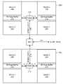
- FIG. 1Ashows a system of a plurality of memory devices that are serially connected to each other, as described in U.S. Patent Publication No. 20070076479.
- a serial interconnection 5includes a plurality of memory devices that are connected in series with a memory controller.
- the memory controllerincludes a system interface for receiving system commands and data from the system in which the serial interconnection is integrated, and provides read data to the system.
- Device 0is comprised of a plurality of data input ports (SIP 0 , SIP 1 ), a plurality of data output ports (SOP 0 , SOP 1 ), a plurality of control input ports (IPE 0 , IPE 1 ), and a plurality of control output ports (OPE 0 , OPE 1 ). These data and control signals are sent to the memory device 5 from the memory controller.
- a second memory device (Device 1 )is comprised of the same types of ports as Device 0 .
- Device 1is interconnected to Device 0 .
- Device 1can receive data and control signals from Device 0 .
- One or more additional devicesmay also be interconnected alongside Device 0 and Device 1 in a similar manner.
- a last device (e.g., Device 3 ) in the series-connectionprovides data and control signals back to the memory controller after a predetermined latency.
- Each memory devicee.g., device 0 , 1 , 2 , 3
- the signalscan be passed from one device to a subsequent series-connected device.
- a single clock signalis provided to each of the plurality of series-connected memory devices.
- FIG. 1Bis a block diagram illustrating the core architecture of one of the memory devices shown in FIG. 1A .
- Memory device 10includes a multiplicity of identical memory banks with their respective data, control and addressing circuits, such as memory bank A 12 and memory bank B 14 , an address and data path switch circuit 16 connected to both memory banks 12 and 14 , and identical interface circuits 18 and 20 , associated with each memory bank for providing data to and for receiving data from the switch circuit 16 .
- Memory banks 12 and 14are preferably non-volatile memory, such as Flash memory, for example. Logically, the signals received and provided by memory bank 12 are designated with the letter “A”, while the signals received and provided by memory bank 14 are designated with the letter “B”.
- each of the interface circuits 18 and 20receives access data in a serial data stream, where the access data can include a command, address information and input data for programming operations, for example. In a read operation, each of the interface circuits provides output data as a serial data stream in response to a read command and address data.
- the memory device 10further includes global circuits, such as a control interface 22 and status/ID register circuit 24 , which provide global signals such as clock signal sclki and reset to the circuits of both memory banks 12 and 14 and the respective interface circuits 18 and 20 .
- Memory bank 12includes well known memory peripheral circuits such as sense amplifier and page buffer circuit block 26 for providing output data DOUT_A and for receiving input program data DIN_A, and row decoder block 28 .
- block 26also includes column decoder circuits.
- a control and predecoder circuit block 30receives address signals and control signals via signal line ADDR_A, and provides predecoded address signals to the row decoders 28 and the sense amplifier and page buffer circuit block 26 .
- the peripheral circuits for memory bank 14are identical to those previously described for memory bank 12 .
- the circuits of memory bank Binclude a sense amplifier and page buffer circuit block 32 for providing output data DOUT_B and for receiving input program data DIN_B, a row decoder block 34 , and a control and predecoder circuit block 36 .
- Control and predecoder circuit block 36receives address signals and control signals via signal line ADDR_B, and provides predecoded address signals to the row decoders 34 and the sense amplifier and page buffer circuit block 36 .
- Each memory bank and its corresponding peripheral circuitscan be configured with well known architectures.
- each memory bankis responsive to a specific command and address, and if necessary, input data.
- memory bank 12provides output data DOUT_A in response to a read command and a read address, and can program input data in response to a program command and a program address.
- Each memory bankcan be responsive to other commands such as an erase command, for example.
- path switch 16is a dual port circuit which can operate in one of two modes for passing signals between the memory banks 12 and 14 , and the interface circuits 18 and 20 .
- Firstis a direct transfer mode where the signals of memory bank 12 and interface circuit 18 are passed to each other. Concurrently, the signals of memory bank 14 and interface circuit 20 are passed to each other in the direct transfer mode.
- Secondis a cross-transfer mode where the signals of memory bank 12 and interface circuit 20 are passed to each other. At the same time, the signals of memory bank 14 and interface circuit 18 are passed to each other.
- a single port configuration of path switch 16will be discussed later.
- interface circuits 18 and 20receive and provide data as serial data streams. This is for reducing the pin-out requirements of the chip as well as to increase the overall signal throughput at high operating frequencies. Since the circuits of memory banks 12 and 14 are typically configured for parallel address and data, converting circuits are required.
- Interface circuit 18includes a serial data link 40 , input serial to parallel register 42 , and output parallel to serial register 44 .
- Serial data link 40receives serial input data SIP 0 , an input enable signal IPE 0 and an output enable signal OPE 0 , and provides serial output data SOP 0 , input enable echo signal IPEQ 0 and output enable echo signal OPEQ 0 .
- Signal SIP 0 (and SIP 1 )is a serial data stream which can each include address, command and input data.
- Serial data link 40provides buffered serial input data SER_IN 0 corresponding to SIPO and receives serial output data SER_OUT 0 from output parallel to serial register 44 .
- the input serial-to-parallel register 42receives SER_IN 0 and converts it into a parallel set of signals PAR_IN 0 .
- the output parallel-to-serial register 44receives a parallel set of output data PAR_OUT 0 and converts it into the serial output data SER_OUT 0 , which is subsequently provided as data stream SOP 0 .
- Output parallel-to-serial register 44can also receive data from status/ID register 24 for outputting the data stored therein instead of the PAR_OUT 0 data. Further details of this particular feature will be discussed later.
- serial data link 40is configured to accommodate daisy chain cascading of the control signals and data signals with another memory device 10 .
- Serial interface circuit 20is identically configured to interface circuit 18 , and includes a serial data link 46 , input serial-to-parallel register 48 , and output parallel-to-serial register 50 .
- Serial data link 46receives serial input data SIP 1 , an input enable signal IPE 1 and an output enable signal OPE 1 , and provides serial output data SOP 1 , input enable echo signal IPEQ 1 and output enable echo signal OPEQ 1 .
- Serial data link 46provides buffered serial input data SER_IN 1 corresponding to SIP 1 and receives serial output data SER_OUT 1 from output parallel-to-serial register 50 .
- the input serial-to-parallel register 50receives SER_IN 1 and converts it into a parallel set of signals PAR_IN 1 .
- the output parallel-to-serial register 48receives a parallel set of output data PAR_OUT 1 and converts it into the serial output data SER_OUT 1 , which is subsequently provided as data stream SOP 1 .
- Output parallel to serial register 48can also receive data from status/ID register 24 for outputting the data stored therein instead of the PAR_OUT 1 data.
- serial data link 46is configured to accommodate daisy chain cascading of the control signals and data signals with another memory device 10 .
- Control interface 22includes standard input buffer circuits, and generates internal chip select signal chip_sel, internal clock signal sclki, and internal reset signal reset, corresponding to chip select (CS#), serial clock (SCLK) and reset (RST#), respectively. While signal chip_sel is used primarily by serial data links 40 and 46 , reset and sclki are used by many of the circuits throughout memory device 10 .
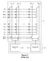
- serial data interfaceprovides performance advantages over parallel data interface architectures, these advantages can be offset by performance degradations in memory banks 12 and 14 . More specifically, the push for increased memory density will adversely affect how quickly data can be sensed from the memory cells, especially NAND configured Flash memory cells. To illustrate this problem, a portion of a NAND configured Flash memory array of FIG. 1B is shown in FIG. 2 .
- memory bank 12includes i sets of bitlines, where i is an integer number greater than 0, and each set includes an even bitline and an odd bitline.
- bitline set 1includes even bitline BL 1 _e and odd bitline BL 1 _o.
- Each bitlineis connected to at least one NAND cell string, where each NAND cell string includes a plurality of non-volatile memory cells and access transistors connected in series between the respective bitline and a common source line CSL.
- the access transistorsinclude a source select transistor for receiving a source select line signal SSL, and a ground select transistor for receiving a ground select line signal GSL.
- Flash memory cellsConnected serially between these two access transistors are a plurality of non-volatile memory cells, such as Flash memory cells.
- Flash memory cellsthere are 32 serially connected Flash memory cells, having gate terminals coupled to respective wordlines WL 1 to WL 32 .
- Sense amplifier and page buffer circuit block 26includes i page buffer units 60 , or one for each bitline set. Because the bitline pitch is narrow, a page buffer unit 60 is shared between the even and odd bitlines of a bitline set. Therefore selection transistors receiving even and odd selection signals BSLe and BLSo are required for selecting one bitline of the set to be coupled to the page buffer unit 60 .
- Each page buffer unit 60senses and latches data from the bitlines, and those skilled in the art will understand that the page buffer latches write data to be programmed.
- Each NAND cell string sharing common wordlines WL 1 -WL 32 , SSL, and GSL linesis referred to as a memory block, while the memory cells connected to one common wordline is referred to as a page. Those skilled in the art should understand how Flash read, program and erase operations are executed.
- FIG. 3is a circuit schematic of column select circuits of the sense amplifier and page buffer circuit block 26 for coupling data in the page buffer units 60 of FIG. 2 to data lines.
- the present example of FIG. 3illustrates one possible logical decoding scheme, where a preset number of page buffers are associated with each of 16 data lines DL 1 to DL 16 .
- there are 16 identically configured dataline decoder circuits 70one being coupled to each of datalines DL 1 to DL 16 .
- the following descriptionrefers to the dataline decoder circuit 70 coupled to DL 1 .
- Dataline decoder circuit 70includes 16 groupings of 32 page buffer units 60 .
- the input/output terminal of one page buffer unitis coupled to a respective first stage n-channel pass transistor 72 .
- All the first stage n-channel pass transistorsare connected in parallel and controlled by first stage selection signals YA 1 to YA 32 to selectively couple one page buffer unit 60 to one second stage n-channel pass transistor 74 . Since there is one second stage n-channel pass transistor 74 per grouping, there are a total of 16 second stage n-channel pass transistors 74 connected in parallel to DL 1 , each controlled by respective second stage selection signals YB 1 to YB 16 .
- the cell data in the selected pageshould be sensed and latched in their corresponding page buffer units 60 .
- Column decodingselects which page buffer units to couple to the datalines.
- Sensingis dependent on the cell current generated by a selected memory cell, and the cell current is dependent on the number of cells in the NAND cell string. In the example of FIG. 2 , the cell current is typically less than 1 ( ⁇ A) for a 32 cell NAND string manufactured with a 90 nm process technology.
- ⁇ A1
- the push to increase memory array density to lower device costresults in the addition of more memory cells per NAND cell string. As a result, this cell current will further decrease, thereby requiring more sensitive sensing circuits and/or sensing time.
- bitline RC delaydue to the physical length of the bitline, and junction capacitance of the NAND cell string as the number of cells per NAND cell string is increased.
- One possible solution to this problemmay be to limit the number of memory cells per NAND cell string, and divide large memory arrays into multiple memory banks.
- An advantage of having multiple memory banksis the capability of transferring data directly between the memory banks without having to transfer data out from the memory device.
- the disadvantage of using multiple memory banksis that each bank requires its own set of sense amplifier and page buffer circuit block 26 , thereby increasing additional circuit overhead and chip area.
- the complex circuitry and area overhead required for implementing direct bank to bank data transferalso consumes additional chip area.
- the present inventionprovides a memory system.
- the memory systemincludes a memory bank and a serial data path.
- the memory bankprovides serial bitstream read data in response to a read operation and receives serial bitstream write data in response to a write operation.
- the serial data pathcouples the serial bitstream read data and the serial bitstream write data between the memory bank and an input/output interface.
- the serial data pathincludes a data arbitrator for receiving access data serially from the input/output interface, the access data including a command and an address. The data arbitrator converts the command and the address into a parallel format and passes the serial bitstream read data to the input/output interface during the read operation.
- the memory bankincludes a first bank half, a second bank half and a parallel/serial data converter.
- the first bank halfis coupled to first n parallel datalines, where n is an integer value greater than 0.
- the second bank halfis coupled to second n parallel datalines.
- the parallel/serial data converterselectively converts one of the first and the second n parallel datalines into the serial bitstream read data and selectively converts the serial bitstream write data into parallel data for one of the first and the second n parallel datalines.
- the first bank halfincludes a first sector, a second sector and a first page buffer.
- the first sectorhas wordlines and bitlines coupled to memory cells.
- the second sectorhas wordlines and bitlines coupled to memory cells.
- the first page bufferis selectively coupled to bitlines of one of the first sector and the second sector, and is coupled to the first n parallel datalines.
- the second bank halfincludes a third sector, a fourth sector and a second page buffer.
- the third sectorhas wordlines and bitlines coupled to memory cells.
- the fourth sectorhas wordlines and bitlines coupled to memory cells.
- the second page bufferis selectively coupled to bitlines of one of the third sector and the fourth sector, and is coupled to the second n parallel datalines.
- bitlines of the first sector and the second sectorare grouped into sets of bitlines, where each of the sets of bitlines are coupled to a common bitline, and the common bitline is coupled to the first page buffer.
- bitlines of the third sector and the fourth sectorare grouped into sets of bitlines, where each of the sets of bitlines is coupled to a common bitline, and the common bitline is coupled to the second page buffer.
- the parallel/serial data converterincludes a first parallel/serial data converter, a second parallel/serial data converter and a data path selector.
- the first parallel/serial data convertersequentially couples each of the first n parallel datalines to a first terminal.
- the second parallel/serial data convertersequentially couples each of the second n parallel datalines to a second terminal.
- the data path selectorselectively couples one of the first terminal and the second terminal to a bidirectional serial data line.
- the memory systemcan further include control logic for receiving a command and an address for operating the memory bank, the parallel/serial converter and the serial data path during the read operation.
- the memory systemfurther includes another memory bank for providing the serial bitstream read data in response to the read operation and for receiving the serial bitstream write data in response to the write operation.
- the serial data pathincludes a data switcher for selectively coupling the serial bitstream write data to one of the memory bank and the other memory bank.
- the serial data pathselectively couples the serial bitstream read data from one of the memory bank and the other memory bank to the data arbitrator of the serial data path.
- the memory systemfurther includes another serial data path for coupling the serial bitstream read data from one of the memory bank and the other memory bank to another input/output interface. The other serial data path also couples the serial bitstream write data to one of the memory bank and the other memory bank.
- the other serial data pathcan include a second data switcher for selectively coupling the serial bitstream write data to one of the other memory bank and the data switcher, and for selectively coupling the serial bitstream read data to one of the data switcher and another data arbitrator.
- a serial transfer datalineis provided for coupling the data switcher to the second data switcher.
- the memory systemcan further include a serial transfer switch for selectively coupling the serial bitstream read data from one of the memory bank and the other memory bank to the serial data path.
- the present inventionmay provide a method for use in a memory system.
- the methodincludes: providing serial bitstream read data in response to a read operation and receiving serial bitstream write data in response to a write operation; and coupling the serial bitstream read data and the serial bitstream write data between the memory bank and an input/output interface.
- the present inventionprovides a memory bank.
- the memory bankincludes a memory array, a page buffer and a sequential coupler.
- the memory arrayhas memory cells connected to bitlines and wordlines.
- the page bufferlatches data of the bitlines during a read operation, and couples the latched data to a predetermined number of datalines in parallel.
- the sequential couplersequentially couples each of the predetermined number of datalines to a bidirectional serial data line.
- the sequential couplercan include a parallel/serial data converter having terminals coupled to each of the predetermined number of datalines.
- the parallel/serial data converteris controllable to sequentially couple each of the terminals to the bidirectional serial data line.
- the memory bankcan further include a counter responsive to a clock signal for controlling the first parallel/serial data converter and the second parallel/serial data converter.
- the data path selectoris controlled by a most significant bit of the counter not used by first parallel/serial data converter and the second parallel/serial data converter.
- the sequential couplercan include a first parallel/serial data converter, a second parallel/serial data converter and a data path selector.
- the first parallel/serial data converterhas first terminals coupled to each of the predetermined number of datalines, and the first parallel/serial data converter is controllable for sequentially coupling each of the first terminals to a first local bidirectional serial data line.
- the second parallel/serial data converterhas second terminals coupled to each of the predetermined number of second datalines, and the second parallel/serial data converter is controllable for sequentially coupling each of the second terminals to a second local bidirectional serial data line.
- the data path selectorselectively couples one of the first local bidirectional serial data line and the second local bidirectional serial data line to a global bidirectional serial data line.
- the present inventionmay provide a method for use a memory array having memory cells connected to bitlines and wordlines.
- the methodincludes: latching data of the bitlines during a read operation, and for coupling the latched data to a predetermined number of datalines in parallel; and sequentially coupling each of the predetermined number of datalines to a bidirectional serial data line.
- the present inventionprovides a memory bank.
- the memory bankincludes a first memory sector, a second memory sector and a page buffer.
- the first memory sectorhas memory cells connected to first bitlines and first wordlines, where the first bitlines are arranged as m segments where m is an integer value greater than 0.
- the second memory sectorhas memory cells connected to second bitlines and second wordlines, where the second bitlines being arranged as m segments.
- the page bufferselectively couples one of the first bitlines and the second bitlines of each of the m segments to a predetermined number of datalines.
- a read operationis executed by activating a wordline of one of the first wordlines in the first memory sector and the second wordlines in the second memory sector in response to a row address, where at least two memory cells are coupled to the first bitlines when the wordline is one of the first wordlines, and at least two memory cells are coupled to the second bitlines when the wordline is one of the second wordlines; selectively coupling one bitline of the first bitlines and the second bitlines to a common bitline in response to a column address; sensing the common bitline with the page buffer; and providing data corresponding to the sensed common bitline onto one of the predetermined number of datalines.
- the present inventionmay provides a method for use in a memory bank having memory cells connected to first bitlines and first wordlines, the first bitlines being arranged as m segments where m is an integer value greater than 0.
- the methodincludes: selectively coupling one of the first bitlines and the second bitlines of each of the m segments to a predetermined number of datalines.
- the present inventionprovides a page buffer for a memory bank.
- the page bufferincluding a first self-decoding page buffer stage and a second self-decoding page buffer stage.
- the first self-decoding page buffer stagesenses data from a first set of common bitlines, and provides sensed data.
- the sensed datacorresponds to each of the common bitlines of the first set of common bitlines, which are provided on corresponding data lines in response to an active column select bit latched in a clock signal state.
- the second self-decoding page buffer stagesenses data from a second set of common bitlines, and provides sensed data.
- the sense datacorresponds to each of the common bitlines of the second set of common bitlines, which are provided on the corresponding data lines in response to the active column select bit latched in a subsequent clock signal state.
- a self-decoding operationis executed by latching the active column select bit in the first self-decoding page buffer stage in response to an opposite clock signal state; providing the sensed data from the first self-decoding page buffer stage and passing the active column select bit in response to the clock signal state; latching the active column select bit in the second self-decoding page buffer stage in response to a subsequent opposite clock signal state; and providing the sensed data from the second self-decoding page buffer stage in response to the subsequent clock signal state.
- the present inventionmay provide a method for use in a page buffer for a memory bank.
- the methodincludes: sensing data from a first set of common bitlines, and for providing sensed data corresponding to each of the common bitlines of the first set of common bitlines on corresponding data lines in response to an active column select bit latched in a clock signal state; and sensing data from a second set of common bitlines, and for providing sensed data corresponding to each of the common bitlines of the second set of common bitlines on the corresponding data lines in response to the active column select bit latched in a subsequent clock signal state.
- the present inventionprovides a system.
- the systemincludes a memory controller for providing access data and a serial interconnection of a plurality of memory devices.
- Each of the memory devicesincludes a controller, a memory bank and a serial data path.
- the controllerreceives the access command and an address contained in access data, for executing an operation corresponding to the access command.
- the memory bankexecutes the operation in accordance with the access command to access data stored in a memory location addressed by the address.
- the serial data pathcouples the data in serial format between the memory bank and an input/output interface.
- the plurality of memory devicesare connected in series and the memory controller sends the access command of an instruction, such as for example, read and write commands.
- an instructionsuch as for example, read and write commands.
- the memory deviceperforms a data read operation and forwards the read data to a next memory device or the memory controller.
- a write operationthe memory device performs a data write operation based on data provided by the memory controller or a previous memory device.
- the system, the memory controller and the devicesmay perform such methods as operating the controller and devices.
- FIG. 1Ashows a system of a plurality of memory devices serially connected to each other
- FIG. 1Bis a block diagram of a memory device having a serial data interface
- FIG. 2is a circuit schematic showing NAND cell strings coupled to a sense amplifier and page buffer circuit block of FIG. 1B ;
- FIG. 3is a circuit schematic showing a column decoding scheme used with the amplifier and page buffer circuit block shown in FIG. 2 ;
- FIG. 4Ais a block diagram of a non-volatile memory serial core system according to an embodiment of the present invention.
- FIG. 4Bis a block diagram of illustration of details of a serial data path shown in FIG. 4A ;
- FIG. 5is a block diagram of a memory bank of FIG. 4A , according to an embodiment of the present invention.
- FIG. 6is a circuit schematic embodiment of the parallel/serial data converter shown in FIG. 5 ;
- FIG. 7Ais a block diagram showing details of two sectors of the memory bank of FIG. 5 ;
- FIG. 7Bis a circuit schematic embodiment showing the bitline arrangement of the sectors shown in FIG. 5 ;
- FIG. 8is a circuit schematic embodiment of a decoding circuit for controlling the bitline selection circuit of FIG. 7 ;
- FIG. 9is a circuit schematic of the charge pump shown in FIG. 8 ;
- FIG. 10is a block diagram showing a self-decoding column select circuit, according to an embodiment of the present invention.
- FIG. 11is a block diagram showing the details of one self-decoding page buffer cell, according to an embodiment of the present invention.
- FIG. 12is a circuit schematic of a sequential enabler in the self-decoding page buffer cell of FIG. 11 , according to an embodiment of the present invention.
- FIG. 13is a circuit schematic of a page buffer unit in the self-decoding page buffer cell of FIG. 11 , according to an embodiment of the present invention.
- FIG. 14is a sequence diagram illustrating the operation of the self-decoding column select circuit of FIG. 10 ;
- FIG. 15is a block diagram illustrating a two bank configuration having a serial core architecture, according to an embodiment of the present invention.
- FIG. 16is a circuit schematic of the serial transfer switch shown in FIG. 15 , according to an embodiment of the present invention.
- FIG. 17is a block diagram of a multi-bank serial core memory system having two independent serial data paths, according to an embodiment of the present invention.
- the present inventionprovides a memory system having a serial data interface and a serial data path core for receiving data from and for providing data to at least one memory bank as a serial bitstream.
- the memory bankis divided into two halves, where each half is divided into upper and lower sectors. Each sector provides data in parallel to a shared two-dimensional page buffer with an integrated self column decoding circuit.
- a serial to parallel data converter within the memory bankcouples the parallel data from either half to the serial data path core.
- the shared two-dimensional page buffer with the integrated self column decoding circuitminimizes circuit and chip area overhead for each bank, and the serial data path core reduces chip area typically used for routing wide data buses. Therefore a multiple memory bank system is implemented without a significant corresponding chip area increase when compared to a single memory bank system having the same density.
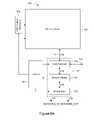
- FIG. 4Ais a block diagram of a non-volatile memory serial core system according to an embodiment of the present invention.
- Serial core memory system 100includes a serial data path 102 for coupling a serial bitstream of data between external input/output interface pins called the DATA/CMD_IN and DATA/CMD_OUT pins and at least one memory bank 104 .
- a memory bankis understood to include pitch-limited circuits, such as row decoders, sense amplifiers, page buffers, column decoding circuitry, and any other circuits which are formed proximate to the rows and columns of memory cells that make up the memory array.
- serial core memory system 100includes a control block 106 and a high voltage generator 108 for providing the necessary voltage levels needed to program and erase the non-volatile memory cells of memory bank 104 .
- the control block 106includes a command decoder, registers, and other related control circuits (not shown) that are used to govern operation of the serial core memory system 100 .
- the memory bank 104is configured to provide read data and to receive write data (for programming), in a serial bitstream.
- both the read data and the write datashare a bidirectional serial data line 110 , however alternate embodiments can have dedicated input and output unidirectional data lines.
- the serial data path 102receives the serial read data and passes it to the DATA/CMD_OUT pin in the serial format, and passes serial write data to the memory bank 104 received from the DATA/CMD_IN pin. Therefore, in both read and write operations, the data is maintained in the serial format between the memory bank and the data I/O pins. Further details of the serial data path 102 will now be described.
- the serial data path 102is primarily responsible for coupling read or write data in a serial format between the memory bank 104 and either of the DATA/CMD_IN pin and the DATA/CMD_OUT pin.
- the serial data path 102can selectively couple read or write data between two or more memory banks and either the DATA/CMD_IN pin and the DATA/CMD_OUT pin.
- the serial data path 102can couple read data directly between two different memory banks.
- the serial data path 102includes a serial I/O interface 112 , a data arbitrator 114 , and a data switcher 116 .
- FIG. 4Bshows details of the serial data path 102 shown in FIG. 4A .
- the serial I/O interface 112is connected directly to the DATA/CMD_IN and the DATA/CMD_OUT pins.
- the serial I/O interface 112can be similarly configured to the serial data link 40 of FIG. 1B and include the same circuitry described for it in U.S. Patent Publication No. 20070076479. In the present example, additional control input signals shown in serial data link 40 of FIG. 1B are not shown in order to simplify the schematic.
- the serial I/O interface 112receives and buffers the externally received input data signals, and can include pass through circuits for directly coupling data from the DATA/CMD_IN pin to the DATA/CMD_OUT pin. This feature is used to pass any command with optional data to another memory device if the command is not intended for the current memory device.
- the serial I/O interface 112includes input buffers 120 for receiving serial input data from its DATA/CMD_IN pin, and output buffers or output driver 122 for providing read data and pass through data through its DATA/CMD_OUT pin.
- the input buffers 120 and output drivers 122are controlled by one or more buffer control signals received from the control block 106 , referred to as B_CTRL in FIG. 4A .
- the data arbitrator 114receives the serial data from the serial I/O interface 112 .
- the data arbitrator 114includes a command data converter 124 and a path switch 126 .
- the command data converter 124converts only the command data from the serial format into a parallel format, which is then sent to the control block 106 as parallel command signal COMMAND.
- the path switch 126selectively connects the serial I/O interface 112 to either the command data converter 124 of the data switcher 116 in response to a switch signal from the control block 106 (not shown).
- Command data converter 124can include a serial/parallel shift register that serially receives the command data on each active clock edge, and has parallel outputs from each stage of the shift register for providing the parallel command.
- Serial/parallel shift registersare known in the art. Since the data structure of the access data is predetermined, for example the command data can be the first two bytes followed by write data, the control block 106 will know when all the command data bits have been loaded into the command data converter 124 by counting the number of clock edges that have passed. Any write data that is received remains in the serial format, and is passed serially to the data switcher 116 . Accordingly, command data converter 124 will only receive the command data while the data switcher will only receive the write data.
- the data switcher 116includes another path switch 128 which is controlled by signal SWTCH from the control block 106 , to couple serial data between the memory bank and the data arbitrator 114 , or to couple serial data between two different memory banks via corresponding serial transfer dataline 118 . If there are no other memory banks on the chip, then data switcher 116 is not required and the serial data is provided directly to memory bank 104 from data arbitrator 114 .
- serial core memory system 100in a read and a write/program operation is now described.
- a serial read commandis received at the DATA/CMD_IN pin, which is then converted into the parallel format and sent to the controller 106 by data arbitrator 114 .
- the controller 106then activates the appropriate rows and columns in the memory bank 104 to access the desired data.
- the memory bank 104is then controlled to provide the read data in a serial bitstream to the data switcher 116 .
- the data switcher 116will be controlled to pass the read data to the data arbitrator 114 , which simply passes the read data to the serial I/O interface 112 for output via the DATA/CMD_OUT pin.
- serial data received on the DATA/CMD_IN pinincludes a command and write data.
- the command dataincludes address data to which the write data is to be programmed.
- the command datais converted to the parallel format by data arbitrator 114 and passed to control block 106 . It is noted that the command is received before the write data in the serial bitstream, so that decoding of the command can be executed for initiating circuits for the programming operation as the write data is passed to the memory bank 104 . Because the control block 106 has received a program command, the appropriate programming algorithms are executed and the proper program voltages are applied, to ensure that the write data is programmed to the target address. Additional algorithms such as program verify will also be executed to repeat the programming, if necessary.
- the memory bank 104provides and receives serial data.
- memory arrayssuch as Flash memory are inherently parallel in nature. This means that more than one bit of data is accessed from the memory array and written to the memory array in any single read or write operation, respectively.
- an internal parallel/serial converteris provided for converting serial data into a parallel format, and vice versa. More specifically, read data provided in parallel from bitlines of the memory array is converted into serial format, and serial write data is converted into parallel format for simultaneous application to bitlines of the memory array.
- the memory bank 104is configured to maximize wordline and bitline performance by segmenting the memory array into sections along both the wordline and the bitline directions.
- FIG. 5is a block diagram illustrating an example embodiment of the memory bank 104 of FIG. 4A , according to an embodiment of the present invention.
- Memory bank 200is divided into four memory portions, shown as sectors (sector 1 , sector 2 , sector 3 and sector 4 ) 202 , 204 , 206 and 208 .
- each sectorincludes bitlines extending in the vertical direction and wordlines extending in the horizontal direction.
- the memory cellscan be organized as Flash NAND cell strings similar to those shown in FIG. 2 .
- each sectorincludes a wordline driver block 210 , which can include associated decoding logic for activating a selected wordline during read and program operations.
- the wordline driver blocks 210 corresponding to sectors 202 and 204activate the same logical wordline of a row in response to a row address within a first address range
- the wordline driver blocks 210 corresponding to sectors 206 and 208activate the same logical wordline of a row in response to a row address within a second address range.
- the rows of memory bank 200are accessed in the same manner as a traditional memory array consisting of a single large sector having the same number of rows.
- wordline performanceis improved since each wordline row is divided into shorter segments that are driven by their own wordline driver blocks 210 .
- the central location of the wordline driver blocks 210divide the memory bank into left and right bank halves, where sectors 202 and 206 form the left half and sectors 204 and 208 form the right half.
- sectors 202 and 206For sensing bitline data and latching program data, sectors 202 and 206 have their bitlines coupled to shared page buffer 212 , while sectors 204 and 208 have their bitlines coupled to shared page buffer 214 . Accordingly, sectors 202 and 204 can be referred to as lower sectors while sectors 206 and 208 can be referred to as upper sectors.
- Page buffers 212 and 214are configured to be selectively coupled to one of an upper sector and a lower sector, thereby overcoming the need to have separate sets of page buffers for each sector. This contributes to the area minimization of the area of memory bank 200 . Further details of the shared page buffers 212 and 214 will be described later.
- Page buffers 212 and 214sense and latch in parallel, bitline data in response to an activated wordline during a read operation.
- the data associated with the memory cells connected to a single wordlineis commonly referred to as a page of data.
- page buffer 212senses and latches a first half page of data
- page buffer 214senses and latches a second half page of data.
- the page buffers 212 and 214sense and latch the bitline data in parallel upon activation of the selected wordline. Once latched, this read data will eventually be output as a serial bitstream.
- a first set of input/output datalinesis coupled to page buffer 212
- a second set of input/output datalinesis coupled to page buffer 214 .
- the width of the sets of datalineswill be n bits wide, where n is an integer value greater than 1.
- a parallel/serial data conversion selector (P/SCS) 216which functions as a sequential coupler, that is coupled to the sets of datalines coupled to page buffers 212 and 214 .
- the parallel/serial data conversion selector 216is placed such that both sets of datalines are the same physical length, and preferably a minimum physical length to minimize loading capacitance.
- the parallel/serial conversion selector 216converts parallel data from the shared buffer 212 to serial format onto dataline 110 or converts parallel data from the shared buffer 214 to serial format onto bidirectional serial dataline 110 . More specifically, each of the n datalines is sequentially coupled to the single bidirectional serial data line 110 as a signal called GLOB_DATA.
- the parallel/serial conversion selector 216converts serial data on bidirectional serial data line 110 to parallel format for the n datalines coupled to shared page buffer 212 or shared page buffer 214 .
- the parallel/serial conversion selector 216is controlled to couple each of the n datalines corresponding to page buffer 212 to bidirectional serial data line 110 , followed by each of the n datalines corresponding to page buffer 214 .
- FIG. 5shows a memory bank 200 having left and right halves.
- the memory arrayincludes only two sectors, such as sectors 202 and 206 .
- Sector 206can thus be the aggregate size of sectors 206 and 208 and sector 202 can be the aggregate size of sectors 202 and 204 .
- a full page of datawould be latched by page buffer 212 .
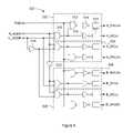
- FIG. 6is a circuit schematic of parallel/serial data converter 216 according to an embodiment of the present invention.
- the P/S data conversion selector 216includes a first parallel/serial data converter (P/SDC) 300 , a second P/SDC 302 , and a data path selector 304 .
- P/SDC 300 and P/SDC 302can be implemented as identical bidirectional n to 1 multiplexor/demultiplexor switches, and data path selector 304 can be implemented as is a bidirectional 2 to 1 multiplexor/demultiplexor switch.
- P/SDC 300selectively couples each of the left side datalines L_DL 1 to L_DLn to the local bidirectional serial data line L_DATA terminal, while P/SDC 302 selectively couples each of the right side datalines R_DL 1 to R_DLn to the local bidirectional serial data line R_DATA terminal.
- Data path selector 304selectively couples either L_DATA or R_DATA to the global bidirectional serial data line 110 as GLOB_DATA.
- a counter 306can be used to provide outputs that are decoded within P/SDC 300 and P/SDC 302 in response to a clocked signal CLK. Such counter decoding schemes should be well known to those of skill in the art.
- L_DATA and R_DATAare n bits in length for one cycle of the counter.
- Data path selector 304is controlled by a selection control signal HALF_SEL to allow all n bits of L_DATA to pass through in one logic state, and to allow all n bits of R_DATA to pass through in the opposite logic state.
- Signal HALF_SELcan be generated by the control block 106 of FIG. 4A in relation to a column address that can select which half of the memory bank 200 is to be accessed.
- counter 306is shared with P/SDC 300 and P/SDC 302 to minimize circuit overhead since dedicated counters would unnecessarily consume chip area.
- a seamless transition between the L_DATA and R_DATA bitsis achieved by coupling signal HALF_SEL to a most significant bit (MSB) that is not used by P/SDC 300 or P/SDC 302 , and will toggle states after the last dataline (L_DLn or R_DLn) is coupled to the L_DATA or R_DATA terminal.
- MSBmost significant bit
- Bit 2remains at the low logic state, while Bit 1 and Bit 2 are used by P/SDC 300 to couple L_DL 1 to L_DL 4 to L_DATA. Starting at state 5, Bit 2 toggles to the high logic state as the counter increments, and remains at the high logic state until state 8. Bit 1 and Bit 2 “restart” at state 5 and gradually increment as in states 1 to 4. Accordingly, Bit 2 is suitable as the HALF_SEL control signal as it inherently controls when data path selector 304 is to switch over from L_DATA to R_DATA.
- FIG. 7Ais an enlarged schematic of sectors 202 and 206 with shared page buffer 212 . More specifically, FIG. 7A illustrates subdivisions of sectors 202 and 206 , referred to as segments. In the present example, sector 202 is divided into four equally sized and identically configured segments 402 while sector 206 is divided into four equally sized and identically configured segments 400 . The selection of four segments per sector is by example only, as those skilled in the art will understand that the number of segments per sector is a design parameter for the memory bank. As will be shown in further detail in FIG.
- each segment 400 and 402includes the same number of bitlines.
- FIG. 7Bis a schematic showing one sector 400 , one segment 402 , and their interconnection with page buffer 212 of shown in FIG. 7A .
- Segments 400 and 402can each provide n bits of data via data lines L_DL[1:n] in any single read operation.
- each segment 400 and 402are arranged as sets of bitlines, and in the present example of FIG. 7B , each set includes even and odd bitlines BL 1 _e/BL 1 _o to BLn_e/BLn_o.
- Each set of even and odd bitlinesis selectively coupled to respective common bitlines CBL_S 1 — 1 to CBL_S 1 _n, and each common bitline is coupled to page buffer 212 .
- the term “S 1 ”indicates that the common bitline CBL belongs to the first segment ( 400 or 402 ) of the sector, and the last digit indicates the specific common bitline of the first segment.
- the bitlines of segment 400are identically configured to those of segment 402 .
- bitline BL 1 _e of segment 402is logically the same as bitline BL 1 _e of segment 400 , as are the other bitlines having common labels.
- the bitlines of segments 402 and 400 in the present configurationare equivalent to a single bitline of memory bank 12 of FIG. 2 .
- the advantage of dividing bitlines into two physical sectionsis that the bitlines of each sector are half as long as the bitlines of memory bank 12 .
- the capacitive loading of the bitlineis significantly reduced.
- each NAND cell stringcan be configured to have more cells, thereby increasing the density of the memory array.
- each set of even and odd bitlines of segments 400 and 402further include a program disable circuit and an even/odd bitline selection circuit coupled thereto.
- the description of these two circuits coupled to BL 1 _e and BL 1 _o of segment 400follows.
- the bitline selection circuit 405includes high voltage n-channel transistors 404 and 406 , where transistor 404 selectively couples BL 1 _e to a common bitline CBL_S 1 _ 1 and transistor 406 selectively couples BL 1 _o to common bitline CBL_S 1 _ 1 .
- Common bitline CBL_S 1 _ 1is connected to page buffer 212 , and to the bitline selection circuit of segment 402 .
- N-channel transistors 404 and 406are controlled by decoded even and odd selection signals A_SELe and A_SELo respectively.
- the prefix “A”denotes signals associated with segment 400
- prefix “B”denotes signals associated with segment 402 . Therefore, during a read or program operation for segment 400 , only one of bitlines BL 1 _e and BL 1 _o will be coupled to page buffer 212 . It is noted that selection signals A_SELe and A_SELo are shared with the other bitline selection circuits in segment 402 .
- the program disable circuit 407includes high voltage n-channel shielding transistors 408 and 410 serially connected between bitlines BL 1 _e and BL 1 _o.
- the common terminal of transistors 408 and 410is connected to a program inhibit voltage level PWRBL, which is selectively coupled to either BL 1 _e and BL 1 _o during either a read or a program operation by activating shielding signals A_SHLDe or A_SHLDo respectively.
- PWRBLprogram inhibit voltage level
- PWRBLwill be set to VSS to bias the unselected bitlines to VSS.
- the corresponding program disable circuit and even/odd bitline selection circuit for BL 1 _e and BL 1 _ois identically configured to the previously described circuits, except that they are controlled by a different set of signals, namely B_SHLDe, B_SHLDo, B_SELe and B_SELo.
- PWRBLcan be driven by an inverter circuit supplied by VCC and VSS, or the program inhibit voltage and VSS, and controlled by a programming related signal. As will be shown in FIG. 8 , a row address is used to generate the selection signals and the shielding signals for either segments 400 or 402 , while a column address is used to generate the even and odd selection and shielding signals.
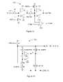
- FIG. 8is an example decoding circuit which can be used for generating the selection signals and the shielding signals for the bitline selection circuit 405 and the program disable circuit 407 in both segments 400 and 402 shown in FIG. 7B .
- FIG. 8is one decoding configuration, and that other decoding configurations can be used for achieving the same result.
- decoding circuit 500includes four identically configured sub-decoders 502 , 504 , 506 and 508 .
- the description of each sub-decoderwill be made with reference to the logic circuits of sub-decoder 502 , since all the sub-decoders are identically configured.
- Each sub-decoder, such as sub-decoder 502includes an address decoding NAND gate 510 , a shield enable NAND gate 512 , inverters 514 and 516 , and local charge pumps 515 and 517 .
- Address decoding NAND gate 510receives a row address R_ADDR and a column address C_ADDR, and provides an output that is provided to one input terminal of shield enable NAND gate 512 and to inverter 516 .
- the output of inverter 516is boosted by local charge pump 517 to provide the even signal A_SELe, which is received by all the bitline selection circuits in segment 400 . Therefore, A_SELe is an address decoded signal driven to the active logic level in response to a particular combination of R_ADDR and C_ADDR. In the present example, this occurs when both R_ADDR and C_ADDR are at the high logic level.
- the second input terminal of shield enable NAND gate 512receives a program status signal PGM, which is decoded with the output of address decoding NAND gate 510 .
- the output of NAND gate 512is driven by inverter 514 and boosted by local charge pump 515 to provide signal A_SHLDe.
- the purpose of the local charge pumpsis to drive the high logic level of the signals above the supply voltage VCC.
- the unselected bitlinesare biased to VSS via PWRBL at VSS.
- one of A_SHLDe or A_SHLDowill be driven to VCC, which is sufficient for discharging the unselected bitline to VSS.
- signals A_SHLDe or A_SHLDo at VCCwill be insufficient for passing the full VCC level to the bitlines. Therefore, the local charge pumps will ensure that the gate terminals of the shielding transistors, such as shielding transistors 408 and 410 , can be driven above VCC.
- bitline selection transistorssuch as transistors 404 and 406 .
- the page bufferwill drive the common bitlines to either VCC or VSS, depending on the data to be programmed.
- signals A_SELe and A_SELoare driven to a voltage level above VCC.
- signal A_SHLDeis a signal that is driven to the active logic level when the particular combination of R_ADDR and C_ADDR is present, i.e., both are at the high logic level.
- C_ADDRis a single bit signal in the present embodiment for coupling one of two bitlines to the common bitline (CBL_S 1 _ 1 _for example)
- the decoding circuit of FIG. 8can be configured to receive C_ADDR of any number of bits.
- one of many bitlinescan be selectively coupled to the common bitline, provided the program disable circuits and the bitline selection circuits are expanded to include more n-channel transistors corresponding to transistors 404 , 406 , 408 and 410 .
- Sub-decoder 504is identically configured to sub-decoder 502 , except that its address decoding NAND gate 510 receives the opposite logic level of C_ADDR via inverter 518 for driving A_SELo to the active logic level and A_SHLDo to the active logic level when PGM is at the active logic level.
- Sub-decoders 502 and 504drive signals for segment 400 since the same row address R_ADDR is used. Therefore sub-decoders 504 and 506 will drive signals B_SELe, B_SHLDe; and B_SELo, B_SHLDo for segment 402 since they receive the opposite state of R_ADDR via inverter 520 . Because sub-decoder 506 receives C_ADDR and sub-decoder 508 receives the opposite state of C_ADDR via inverter 518 , the even and odd selection and shield signals are provided.
- Program status signal PGMis shared by all the shield enable NAND gates 512 of the sub-decoders 502 , 504 , 506 and 508 , to globally enable or disable production of its respective shielding signals.
- PGMis at the active high logic level during a program operation to ensure that the proper shielding signal is activated so that the non-selected bitline adjacent to the selected bitline, is coupled to PWRBL to inhibit programming of memory cells connected to it.
- PWRBLcan be inhibited from being applied to all the bitlines during a read operation, because the non-selected bitline can be subsequently selected by changing the column address C_ADDR while the selected wordline remains active, to read more data from the memory array.
- a read operation and a write operation of the circuits shown in FIG. 7can be easily understood.
- PGMis at the low logic level and a wordline is activated in all the segments, including segments 400 and 402 , of sector 202 or 206 of FIG. 5 .
- a current corresponding to a stored data state in the corresponding memory cellsis then provided to a respective bitline. If the row address activates a wordline in segment 400 , then the selection signals B_SELe, B_SELo, B_SHLDe and B_SHLDo for segment 402 are disabled.
- one of the even or odd bitlines of each set of bitlinesis coupled to a corresponding common bitline.
- the page buffer 212will sense and latch the data of all the common bitlines of the sector, but will provide only the data from one segment in parallel on data lines L_DL[1:n].
- the common datalines L_DL[1:n]are shared by all the segments in sectors 200 and 206 , and as will be described later, the data from exactly one segment is coupled to datalines L_DL[1:n]. More specifically, all the data of either segment 400 or 402 is output by sequentially enabling the page buffer 212 segments to couple data to datalines L_DL[1:n].
- a program operationis the reverse process, except now PGM is at the high logic level.
- Write datawill be provided on data lines L_DL[1:n] to be latched by page buffer 212 and driven onto the respective common bitlines. If a wordline in segment 400 is selected for programming, then the selection signals A_SELe, A_SELo, A_SHLDe and A_SHLDo are disabled. It is noted that since no wordline in segment 402 is selected, there is no need to apply the PWRBL program inhibit voltage to the bitlines, thereby reducing power consumption.
- a column address C_ADDRis provided and the common bitlines will be coupled to the selected bitlines of the even or odd bitlines, while the PWRBL voltage is applied to the non-selected bitlines.
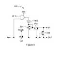
- FIG. 9is a circuit schematic illustrating an example local charge pump used in the sub-decoders of FIG. 8 .
- Local charge pump 550includes a depletion mode n-channel pass transistor 552 , a native n-channel diode-connected boost transistor 554 , a high breakdown voltage n-channel decoupling transistor 556 , a high breakdown voltage n-channel clamp transistor 558 , a NAND logic gate 560 , and a capacitor 562 .
- NAND logic gate 560has one input terminal for receiving input terminal IN and another input terminal for receiving controlled signal ⁇ p, for driving one terminal of capacitor 562 .
- Pass transistor 552is controlled by the complement of signal PGM of FIG. 8 , referred to as PGMb.
- the common terminals of decoupling transistor 556 and clamp transistor 558are coupled to high voltage VH.
- local charge pump 550The operation of local charge pump 550 is now described.
- PGMbis at the high logic level and ⁇ p is maintained at the low logic level. Therefore, circuit elements 562 , 554 , 556 and 558 are inactive, and the output terminal OUT reflects the logic level appearing on the input terminal IN.
- PGMbis at the low logic level, and ⁇ p is allowed to oscillate between the high and low logic levels at a predetermined frequency. If the input terminal IN is at the high logic level, then capacitor 562 will repeatedly accumulate charge on its other terminal and discharge the accumulated charge through boost transistor 554 .
- Decoupling transistor 556isolates VH from the boosted voltage on the gate of boost transistor 554 .
- Clamp transistor 558maintains the voltage level of output terminal OUT at about VH+Vtn, where Vtn is the threshold voltage of clamp transistor 558 .
- the local charge pump 550 shown in FIG. 9is one example circuit which can be used to drive signals to a voltage levels higher than the supply voltage VCC, but persons skilled in the art will understand other charge pump circuits can be used with equal effectiveness. Table 2 below shows example bias conditions for the local charge pump 550 during read and program operations.
- Vcc Vss Vss PGMbVcc Vcc Vss Vss ⁇ P
- Vss Vss Oscillation Oscillation VHVcc Vcc ⁇ 5 V ⁇ 5 V OUT Vcc Vss 5 V + Vtn Vss
- minimized circuit area consumption of the pitch limited circuitswill result in a reduced area of the memory bank.
- thisis achieved by sharing one page buffer with both adjacent sectors 202 and 206 , and by minimizing the amount of column select circuitry used for coupling the page buffer 212 to the datalines L_DL[1:n].
- the previously proposed column decoding scheme shown in FIG. 3can be used to couple the data from the page buffer 212 of FIG. 5 or 7 A to the datalines L_DL[1:n]
- the plurality of first and second stage pass transistorswill require valuable circuit area.
- a self-decoding column select circuitis used for coupling data from each page segment of sectors 202 and 206 to the datalines L_DL[1:n].
- FIG. 10is a block diagram showing a functional implementation of a self-decoding column select circuit integrated into a page buffer circuit, according to an embodiment of the present invention.
- Self-decoding page buffer 600can be used in place of both page buffers 212 and 214 in FIG. 5 and page buffer 212 in FIG. 7 .
- Self-decoding page buffer 600will sequentially couple data from each segment stored in page buffer 212 to the datalines L_DL[1:n], in response to a single column select bit COL_BIT that is shifted through the self-decoding page buffer 600 .
- the self-decoding page buffer 600includes several page buffer stages 614 , 616 and 618 , of which only three are shown in FIG. 10 . As shown in FIG.
- the page buffer stages 614 , 616 and 618include sequential enablers 602 , 604 and 606 , and segment page buffers 608 , 610 and 612 . Accordingly, each sequential enabler is paired with one segment page buffer for controlling the segment page buffer. For example, sequential enabler 602 is paired with segment page buffer 608 .
- sequential enabler 602is paired with segment page buffer 608 .
- FIG. 10it is assumed that there are up to m page segments ( 400 and 402 ) in sectors 202 and 206 of FIG. 7A , and therefore there are m corresponding self-decoding page buffer stages, of which only the first, second and last self-decoding page buffer stages of self-decoding page buffer 600 are shown.
- the variable mcan be any integer value greater than 0, and is selected based on the memory array architecture.
- segment page buffer 608couples common bitlines CBL_S 1 — [1:n] of the first segment to L_DL[1:n]
- segment page buffer 610couples common bitlines CBL_S 2 [1:n] of the second segment to L_DL[1:n]
- segment page buffer 612couples common bitlines CBL_Sm — [0:n] of the mth (last) segment to L_DL[1:n].
- Each segment page bufferis controlled by its respective sequential enabler, and each sequential enabler will be enabled to couple its common bitlines to L_DL[1:n] when the single column select bit COL_BIT is received.
- each sequential enablerreceives control signals such as complementary reset signals RST and RSTb, decode enable signal YENb, and complementary clock signals ⁇ and ⁇ b. In their active states, signals RST, RSTb and YENb enable the sequential enabler.
- the input terminal INreceives COL_BIT, which will be provided through output terminal OUT in response to clock signals ⁇ and ⁇ b.
- column select bit COL_BITis eventually shifted from the first sequential enabler 602 to the last sequential enabler 606 . Therefore, each segment page buffer will couple its common bitlines to L_DL[1:n] in sequence, in response to COL_BIT.
- COL_BITis a high logic level bit, but can be a low logic level bit as well.
- FIG. 11is a block diagram showing the details of one self-decoding page buffer stage, such as self-decoding page buffer stage 614 for example.
- Self-decoding page buffer stage 614includes sequential enabler 602 shown in FIG. 10 , and page buffer units 650 , 652 , 654 and 660 .
- page buffer unit 660is the last page buffer unit in page buffer stage 614 .
- Sequential enabler 602is a simplified block diagram that omits the control signals in order to simplify the diagram.
- page buffer unit 650couples CBL_S 1 _ 1 to L_DL 1 .
- All page buffer unitsare enabled to electrically couple their common bitline to a respective dataline in response to an active column enable signal Y-SEL.
- Y-SELis driven to the active logic level by sequential enabler 602 in response to COL_BIT, which will be subsequently passed on to the next sequential enabler in response to the clock signals ⁇ and ⁇ b (not shown).
- FIG. 12is a circuit schematic of the sequential enabler 602 of FIGS. 10 and 11 .
- Each sequential enableris implemented as a master/slave flip-flop 700 .
- Master/slave flip-flop 700includes a first transmission gate 702 , a pair of cross-coupled inverters 704 and 706 , a second transmission gate 708 , a second pair of cross-coupled inverters 710 and 712 , first and second reset devices 714 and 716 , and a NOR logic gate 718 .
- Master/slave flip-flop 700is enabled when control signals RST, RSTb and YENb are at the high, low and low logic levels, respectively.
- OUT and Y-selWhen disabled, OUT and Y-sel will be at the low logic level as reset devices 714 and 716 will be turned on and at least one input to NOR logic gate 718 will be at the high logic level.
- These control signalscan be controlled by the command decoder or other similar logic, and synchronized to ensure that read data is properly applied to the datalines and program data is properly applied to the common bitlines.
- First transmission gate 702passes a received signal, such as COL_BIT, on input terminal IN when clock signals ⁇ and ⁇ b are at the high and low logic levels respectively.
- Cross coupled inverters 704 and 706will latch the signal and pass it to the second pair of cross-coupled inverters 710 and 712 via second transmission gate 708 when ⁇ and ⁇ b have switched to the low and high logic levels respectively.
- the inverted state of the input signal (COL_BIT)is received by NOR logic gate 718 , which is then inverted again by enabled NOR logic gate 718 to drive Y-sel to the high logic level.
- Output terminal OUTwill pass COL_BIT to the next master/slave flip-flop at substantially the same time that Y-sel is driven to the active high logic level. It is noted, however, that the next master/slave flip-flop will latch COL_BIT when clock signal ⁇ is at the high logic level.
- FIG. 13is a circuit schematic of a page buffer unit, such as page buffer unit 650 shown in FIG. 11 .
- Page buffer unit 750includes a precharge circuit, a sense circuit and a dataline coupling circuit.
- the precharge circuitincludes a precharge device 752 for precharging the common bitline CBL_S[1:m][1:n] to VDD in response to precharge signal PREb.
- the sense circuitincludes a latch reset device 754 , a latch sense enable device 756 , and a latch enable device 758 connected in series between VDD and VSS, and cross-coupled inverters 760 and 762 .
- Latch reset device 754is controlled by latch reset signal RSTPB for resetting the latched state of cross-coupled inverters 760 and 762 .
- Latch enable device 758is controlled by latch enable signal LCHD for enabling sensing of the current on the common bitline CBL_S[1:m][1:n].
- Cross-coupled inverters 760 and 762have a first common node “a” connected to the shared terminals of latch reset device 754 and latch sense enable device 756 , and a second common node “b” coupled to the dataline coupling circuit.
- the dataline coupling circuitincludes a bitline isolation device 764 and a column select device 766 connected in series between common bitline CBL_S[1:m][1:n] and dataline L_DL[1:n], having common node “b” at the shared terminals of devices 764 and 766 .
- Bitline isolation device 764is controlled by signal ISOPB while column select device 766 is controlled by column select signal Y-sel.
- Signals PREb, RSTPB, ISOPB and LCHDcan be generated from the control block 106 of FIG. 4A .
- page buffer unit 650during a read operation is now described. While latch enable signal LCHD is at the inactive low logic level, signal RSTPB is driven to the low logic level to reset cross-coupled inverters 760 and 762 such that node “b” is set to the low logic level. Accordingly, node “a” is at the high logic level during this reset state.
- the common bitline CBL_S[1:m][1:n]is precharged to VDD by driving PREb to the low logic level, thereby turning on precharge device 752 .
- page buffer unit 650during a program operation is now described.
- latch enable signal LCHDis not used and remains at the inactive low logic level, while signal RSTPB is driven to the low logic level to reset cross-coupled inverters 760 and 762 such that node “b” is set to the low logic level.
- the common bitline CBL_S[1:m][1:n]is precharged to VDD by driving PREb to the low logic level, thereby turning on precharge device 752 .
- Program datais driven onto L_DL[1:n], and is latched by cross-coupled inverters 760 and 762 when Y-sel is driven to the high logic level.
- Signal ISOPBis driven to the high logic level to couple node “b” to CBL_S[1:m][1:n]. The programmed state of the memory cells coupled to the selected wordline will then depend on the logic level of node “b”.
- a unique feature of page buffer unit 750is the single column select device 766 that directly couples the cross-coupled inverters 760 and 762 to L_DL[1:n].
- the single column select deviceis simpler and occupies a smaller circuit area than the column select devices 72 and 74 of FIG. 3 . Accordingly, a single corresponding Y-sel signal, generated by a corresponding sequential enabler such as sequential enabler 602 , is all that is needed for coupling L_DL[1:n] to node “b”.
- the previous description of the operation of the page buffer unit 650 during read and program operationsare example operations, and those skilled in the art will understand that the same circuit can be operated with variations in signal activation sequences.
- the page buffer unit 650can be implemented with alternate circuit configurations that perform sensing and latching functionality for read data, and latching functionality for program data.
- control signal tracesinclude common complementary clock signals ⁇ and ⁇ b, common complementary reset signals RST and RSTb, and common decode enable signal YENb.
- the signal traces for the input terminal “In”, the output terminal “Out” and the Y-sel output of a first sequential enablerare shown, as are the signal traces for the output terminal “Out” and the Y-sel output for subsequent sequential enablers.
- the signals associated with the first, second and third sequential enablersare appended with the numbers 1, 2 and 3 respectively, while the last (mth) sequential enabler has its associated signals appended with the letter m.
- reset signal RSTis pulsed to the high logic level while complementary signal RSTb is pulsed to the low logic level to reset all the sequential enablers.
- RST and RSTbare pulsed on a rising edge of clock signal ⁇ .
- the latch consisting of inverters 704 and 706has its input side coupled to VSS while the latch consisting of inverters 710 and 712 has its input side coupled to VDD, in response to the complementary reset signal pulses.
- transmission gate 708is open while clock signal ⁇ is at the high logic level. Therefore the two latch circuits drive each other to the reset states.
- Decode enable signal YENbremains at the inactive high logic level to maintain Y-sel at the low logic level.
- the input terminal In_ 1 of the first sequential enabler 1is pulsed to the high logic level, which corresponds to the application of column select bit COL_BIT.
- COL_BITis latched by inverters 704 and 706 when ⁇ is at the high logic level.
- ⁇transitions to the low logic level to shift COL_BIT to inverters 710 and 712 to drive output terminal “Out” to the high logic level.
- clock signal ⁇transitions to the low logic level and COL_BIT appearing on Out_ 1 will be latched by the sequential enabler 2 , since its In_ 2 input terminal is connected to Out_ 0 .
- YENbis pulsed to the low logic level at time t 4 to enable NOR logic gate 718 , which then drives Y-Sel_ 1 to the high logic level for the same approximate duration that YENb is at the low logic level.
- column select device 766 of page buffer unit 750will be turned on to couple its corresponding common bitline to a dataline.
- clock signal ⁇transitions to the low logic level, causing output terminal Out_ 2 of sequential enabler 2 to be driven to the high logic level.
- sequential enabler 2had received COL_BIT at time t 3 .
- output terminal Out_ 1 of sequential enabler 1falls to the low logic level as it had latched the inactive COL_BIT signal.
- Y-Sel_ 2will be pulsed to the high logic level in response to low logic level pulse of YENb. This process repeats until the last sequential enabler pulses Y-Sel_m to the high logic level.
- Y-Sel_mis the last column select signal of page buffer 212 to be enabled. If the same logical wordline is driven in Sector 208 , then the output terminal Out_m can be coupled to the first sequential enabler in page buffer 214 , where the sequential activation of column select signals would continue.
- parallel/serial data conversion selector 216is controlled to serialize the data from R_DL[1:n] instead of L_DL[1:n]. Therefore, by activating the column enable signals (Y-Sel — [1:m]) in sequence, all the bits of data associated with a selected wordline can either be read from it or programmed to it.
- FIGS. 7A to 13shows their implementations in the serial data path core architecture
- theycan be used in illustrated Flash memory architectures that do not employ a serial data path core architecture.
- the standard Flash memory arraycan be designed to be divided into top and bottom halves, analogous to the sectors shown in the figures, and the page buffer of the presented embodiments positioned in between.
- Column selection devices and decoding circuitry for multiplexing the top bitlines and bottom bitlines to common bitlinescan be implemented in the manner shown and described in the present embodiments. While each self-decoding page buffer cell of the 2D page buffer shown in FIGS.
- any address decoded signalcan be used instead.
- the specific decoding configurationwill depend on the selected data output architecture being implemented. For example, a grouping of successive page buffer units can receive the same address decoded Y-sel signal, or each page buffer unit of a grouping receives a different address decoded Y-sel signal.
- the serial core memory system 100includes two memory banks both accessible by the serial data path 102 .
- the single memory bank 200would be replaced by two identically configured memory banks.
- both memory bankscan be coupled to each other to realize direct bank-to-bank data transfers.
- Bank-to-bank transfersare ideally suited for advanced operations such as wear leveling control, where data can be copied to the other memory bank if the finite program/erase cycles for a portion of the current memory bank is about to be reached.
- FIG. 15is a block diagram showing a direct bank to bank transfer architecture according to an embodiment of the invention.
- the present embodimentincludes two identically configured memory banks 800 and 802 , and a serial transfer switch 804 .
- memory banks 800 and 802are identical in configuration as memory bank 200 of FIG. 5 , and as such, includes the same features that have been previously described.
- Memory bank 800provides and receives serial data via a serial data signal called BANK 1 _DATA while memory bank 802 provides and receives serial data via a serial data signal called BANK 2 _DATA.
- BANK 1 _DATA and BANK 2 _DATAare coupled to serial transfer switch 804 , which selectively couples one of the two to GLOB_DATA depending on which memory bank is being accessed for a read or a program operation.
- GLOB_DATAis analogous to the same named signal in FIG. 5 , which is coupled to a serial data path, such as serial data path 102 of FIG. 5 . While signal GLOB_DATA is considered a serial global data signal that is coupled to the serial data path of a memory device, such as serial data path 102 of FIG. 4A , serial data signals BANK 1 _DATA and BANK 2 _DATA are considered local serial data signals.
- serial transfer switch 804The operation of serial transfer switch 804 described above is called a normal mode of operation.
- BANK 1 _DATA and BANK 2 _DATAare directly coupled to each other.
- the page buffers of memory bank 800 and 802will be synchronized such that data provided from the page buffers of one memory bank are latched in the page buffers of the other memory bank.
- the same clock signals used by the sequential enabler 700 of FIG. 12can be shared between memory banks 800 and 802
- the CLK signal used in parallel/serial data conversion selector 216 of FIG. 6can be shared between memory banks 800 and 802 .
- FIG. 16is a circuit schematic of serial transfer switch 804 of FIG. 15 , according to one embodiment.
- Serial transfer switch 804includes a data bank selector 810 , and transmission gates 812 , 814 and 816 .
- Transmission gate 812couples BANK 1 _DATA to a first terminal of data bank selector 810
- transmission gate 814couples BANK 2 _DATA to a second terminal of data bank selector 810 .
- Both transmission gates 812 and 814are turned on when complementary signals DIR and DIRb are at the inactive low and high logic levels respectively.
- Transmission gate 816couples BANK 1 _DATA and BANK 2 _DATA directly to each other when DIR and DIRb are at the active high and low logic levels respectively.
- Data bank selector 810is controlled by selection signal BANK_SEL, to couple either BANK 1 _DATA or BANK 2 _DATA to GLOB_DATA.
- the circuit of serial transfer switch 804is an example of one circuit implementation, and other known circuits can be used to achieve the same functionality.
- data bank selector 810can be implemented with a multiplexor/demultiplexor circuit that is well known in the art. Signals DIR and DIRb can be generated by the control block 106 of the memory device of FIG. 4A in response to a specific command.
- the direct bank to bank transfer architectureis scalable to include more than two memory banks.
- pairs of memory banks as configured in FIG. 15can be linked together with another serial transfer switch positioned between the two pairs to couple the final GLOB_DATA signal to the serial data path.
- the memory bank configuration shown in FIG. 15can replace the single memory bank 104 of FIG. 4A .
- the serial core memory system 100 of FIG. 4Ais an example of a memory device having a single serial data path for interfacing with other memory devices.
- U.S. Patent Publication No. 20070076479describes a high performance memory system which can execute substantially concurrent operations as it includes a two separate serial interface circuits. This principle can be applied to the serial core memory system 100 of FIG. 4A to realize a high density and high performance memory system with a direct bank to bank transfer architecture.
- FIG. 17is a block diagram of a multi-bank serial core memory system having two independent serial data paths.
- Memory system 900includes a first serial data path 902 , a second serial data path 904 , control blocks 906 and 908 , and memory banks 910 , 912 , 914 and 916 .
- Located between memory banks 910 and 912is a first serial transfer switch 918 .
- Located between memory banks 914 and 916is a second serial transfer switch 920 .
- the first and second serial data paths 902 and 904correspond to the serial data path 10 shown in FIG. 4A
- the control blocks 906 and 908correspond to the control block 106 shown in FIG. 4A .
- the first serial data path 902receives DATA/CMD_IN_ 1 and provides DATA/CMD_OUT_ 1 while second serial data path 904 receives DATA/CMD_IN_ 2 and provides DATA/CMD_OUT_ 2 .
- Each of the first and second serial data paths 902 and 904includes a serial I/O interface 922 , a data arbitrator 924 , and a data switcher 926 . All these circuits have been previously described, as have their functions.
- circuit blocks 902 , 906 , 910 , 912 and 918operate as a single unit, while circuit blocks 904 , 908 , 914 , 916 and 920 operate as another single unit.
- the presence of data switchers 926 in both serial data paths 902 and 904now permits the serial data paths to access every memory bank.
- FIG. 17there is a single bit direct transfer line 928 coupled between data switchers 926 . Therefore, memory banks 910 and 912 can be coupled to serial data path 904 while memory banks 914 and 916 can be coupled to serial data path 902 . Furthermore, data from memory banks 910 and 912 can be directly transferred to memory banks 914 and 916 , and vice versa, through the direct transfer line 928 .
- Direct memory transfer operationsare advantageous, since the data does not need to be read out of the memory device before being reprogrammed to a different bank of the same memory device.
- page copy or block copy operationscan be efficiently executed because as data corresponding to one page is read from a source bank, the data is loaded into the target bank at substantially the same time.
- Secondis the self-decoding column select circuit for quickly transferring data from the bitlines to datalines.
- Secondis the shared page buffer which is coupled to two sectors of a memory array.
- Thirdis the serial data path for coupling a serial bitstream of data between external input/output interface pins and at least one memory bank 104 of FIG. 4A .
- Fourthare the serial transfer switches and data switches that couple memory banks to each other or to different serial data paths. Since data is transferred between the external input/output pins and the memory sectors in serial format, and only converted to parallel format within the memory bank, significant circuit area is conserved. This is because only single bi-directional serial data lines, such as direct transfer line 928 , bidirectional serial data lines 110 and the serial data paths 902 and 904 are used for transporting the data serially instead of with a plurality of parallel data lines.
- serial core memory systemcan be implemented in discrete memory devices, or can be embedded in a system on chip (SOC) or system in package (SIP) device.
- SOCsystem on chip
- SIPsystem in package
- multiple memory devices having the above described serial core memory system embodimentscan be used in the serial interconnection 5 of FIG. 1A .
- a single packaged device implemented as an SOCcan have multiple instances of the memory system connected serially in the same configuration shown in FIG. 1A .
- a single packaged device implemented as an SIPcan have multiple chips connected serially in the same configuration shown in FIG. 1A .
- the operationhas been described based on the active “high” signals for the purpose of simplicity. They may be designed to perform the operation based on the “low” active signals, in accordance with a design preference.
- the device elements and circuitsare coupled or connected to each other as shown in the figures, for the sake of simplicity.
- devices, elements, circuits, etc.may be coupled or connected directly to each other.
- devices, elements, circuits etc.may be coupled or connected indirectly to each other through other devices, elements, circuits, interfaces, etc., necessary for operation of the apparatus.
- the circuit elements and devicesare directly or indirectly coupled with or connected to each other.
Landscapes
- Engineering & Computer Science (AREA)
- Theoretical Computer Science (AREA)
- Microelectronics & Electronic Packaging (AREA)
- Human Computer Interaction (AREA)
- Physics & Mathematics (AREA)
- General Engineering & Computer Science (AREA)
- General Physics & Mathematics (AREA)
- Read Only Memory (AREA)
- Dram (AREA)
- Memory System (AREA)
Abstract
Description
- This application claims the benefit of priority of U.S. Provisional Patent Application No. 60/867,269, filed on Nov. 27, 2006, the content of which is incorporated herein by reference in its entirety.
- Mobile electronic devices, such as, for example, digital cameras, portable digital assistants, portable audio/video players and mobile terminals continue to require mass storage memory, preferably non-volatile memory with ever increasing capacities and speed capabilities. For example, presently available audio players can have between 256 Mbytes to 40 Gigabytes of memory for storing audio/video data. Non-volatile memory, for example, such as Flash memory and hard-disk drives are preferred since data is retained in the absence of power, thus extending battery life.
- Presently, hard disk drives have high densities and can store 40 to 160 Gigabytes of data, but are relatively bulky. However, Flash memory, also known as a solid-state drive, is popular because of their high density, non-volatility, and small size relative to hard disk drives. The advent of multi-level cells (MLC) further increases the Flash memory density for a given area relative to single level cells. Those of skill in the art will understand that Flash memory can be configured as NOR Flash, NAND Flash or any other type of Flash memory configuration. NAND Flash has higher density per given area due to its more compact memory array structure. For the purposes of further discussion, references to Flash memory should be understood as being any type of Flash devices, such as, for example, NOR and NAND type Flash memory.
- While existing Flash memory modules operate at speeds sufficient for many current consumer electronic devices, such memory modules likely will not be adequate for use in future devices where high data rates are desired. For example, a mobile multimedia device that records high definition moving pictures is likely to require a memory module with a programming throughput of at least 10 MB/s, which is not obtainable with current Flash memory technology with typical programming data rates of 7 MB/s. Multi-level cell Flash has a much slower rate of 1.5 MB/s due to the multi-step programming sequence required to program the cells.
- The problem with many standard memory devices lies in their use of a parallel data interface for receiving and providing data. For example, some memory devices provide 8, 16 or 32 bits of data in parallel at an operating frequency of up to 30 MHz. Standard parallel data interfaces providing multiple bits of data in parallel are known to suffer from well known communication degrading effects such as cross-talk, signal skew and signal attenuation, for example, which degrades signal quality, when operated beyond their rated operating frequency. In order to increase data throughput, a memory device having a serial data interface has been disclosed in commonly owned U.S. Patent Publication No. 20070076479, which receives and provides data serially at a frequency, for example, 200 MHz. The memory device described in U.S. Patent Publication No. 20070076479 can be used in a system of memory devices that are serially connected to each other, as described in commonly owned U.S. Provisional Patent Application No. 60/902,003 filed Feb. 16, 2007, the content of which is incorporated herein by reference in its entirety.
FIG. 1A shows a system of a plurality of memory devices that are serially connected to each other, as described in U.S. Patent Publication No. 20070076479. Referring toFIG. 1A , aserial interconnection 5 includes a plurality of memory devices that are connected in series with a memory controller. The memory controller includes a system interface for receiving system commands and data from the system in which the serial interconnection is integrated, and provides read data to the system. In particular,Device 0 is comprised of a plurality of data input ports (SIP0, SIP1), a plurality of data output ports (SOP0, SOP1), a plurality of control input ports (IPE0, IPE1), and a plurality of control output ports (OPE0, OPE1). These data and control signals are sent to thememory device 5 from the memory controller. A second memory device (Device1) is comprised of the same types of ports asDevice 0.Device 1 is interconnected toDevice 0. For example,Device 1 can receive data and control signals fromDevice 0. One or more additional devices may also be interconnected alongsideDevice 0 andDevice 1 in a similar manner. A last device (e.g., Device3) in the series-connection provides data and control signals back to the memory controller after a predetermined latency. Each memory device (e.g.,device FIG. 1B is a block diagram illustrating the core architecture of one of the memory devices shown inFIG. 1A .Memory device 10 includes a multiplicity of identical memory banks with their respective data, control and addressing circuits, such asmemory bank A 12 andmemory bank B 14, an address and datapath switch circuit 16 connected to bothmemory banks identical interface circuits switch circuit 16.Memory banks memory bank 12 are designated with the letter “A”, while the signals received and provided bymemory bank 14 are designated with the letter “B”. Similarly, the signals received and provided byinterface circuit 18 are designated with the number “0”, while the signals received and provided byinterface circuit 20 are designated with the number “1”. Each of theinterface circuits memory device 10 further includes global circuits, such as acontrol interface 22 and status/ID register circuit 24, which provide global signals such as clock signal sclki and reset to the circuits of bothmemory banks respective interface circuits Memory bank 12 includes well known memory peripheral circuits such as sense amplifier and pagebuffer circuit block 26 for providing output data DOUT_A and for receiving input program data DIN_A, androw decoder block 28. Those of skill in the art will understand thatblock 26 also includes column decoder circuits. A control andpredecoder circuit block 30 receives address signals and control signals via signal line ADDR_A, and provides predecoded address signals to therow decoders 28 and the sense amplifier and pagebuffer circuit block 26.- The peripheral circuits for
memory bank 14 are identical to those previously described formemory bank 12. The circuits of memory bank B include a sense amplifier and pagebuffer circuit block 32 for providing output data DOUT_B and for receiving input program data DIN_B, arow decoder block 34, and a control andpredecoder circuit block 36. Control andpredecoder circuit block 36 receives address signals and control signals via signal line ADDR_B, and provides predecoded address signals to therow decoders 34 and the sense amplifier and pagebuffer circuit block 36. Each memory bank and its corresponding peripheral circuits can be configured with well known architectures. - In general operation, each memory bank is responsive to a specific command and address, and if necessary, input data. For example,
memory bank 12 provides output data DOUT_A in response to a read command and a read address, and can program input data in response to a program command and a program address. Each memory bank can be responsive to other commands such as an erase command, for example. - In the example shown in
FIG. 1B ,path switch 16 is a dual port circuit which can operate in one of two modes for passing signals between thememory banks interface circuits memory bank 12 andinterface circuit 18 are passed to each other. Concurrently, the signals ofmemory bank 14 andinterface circuit 20 are passed to each other in the direct transfer mode. Second is a cross-transfer mode where the signals ofmemory bank 12 andinterface circuit 20 are passed to each other. At the same time, the signals ofmemory bank 14 andinterface circuit 18 are passed to each other. A single port configuration ofpath switch 16 will be discussed later. - As previously mentioned,
interface circuits memory banks Interface circuit 18 includes aserial data link 40, input serial toparallel register 42, and output parallel toserial register 44. Serial data link40 receives serial input data SIP0, an input enable signal IPE0 and an output enable signal OPE0, and provides serial output data SOP0, input enable echo signal IPEQ0 and output enable echo signal OPEQ0. Signal SIP0 (and SIP1) is a serial data stream which can each include address, command and input data. Serial data link40 provides buffered serial input data SER_IN0 corresponding to SIPO and receives serial output data SER_OUT0 from output parallel toserial register 44. The input serial-to-parallel register 42 receives SER_IN0 and converts it into a parallel set of signals PAR_IN0. The output parallel-to-serial register 44 receives a parallel set of output data PAR_OUT0 and converts it into the serial output data SER_OUT0, which is subsequently provided as data stream SOP0. Output parallel-to-serial register 44 can also receive data from status/ID register 24 for outputting the data stored therein instead of the PAR_OUT0 data. Further details of this particular feature will be discussed later. Furthermore, serial data link40 is configured to accommodate daisy chain cascading of the control signals and data signals with anothermemory device 10.Serial interface circuit 20 is identically configured to interfacecircuit 18, and includes aserial data link 46, input serial-to-parallel register 48, and output parallel-to-serial register 50. Serial data link46 receives serial input data SIP1, an input enable signal IPE1 and an output enable signal OPE1, and provides serial output data SOP1, input enable echo signal IPEQ1 and output enable echo signal OPEQ1. Serial data link46 provides buffered serial input data SER_IN1 corresponding to SIP1 and receives serial output data SER_OUT1 from output parallel-to-serial register 50. The input serial-to-parallel register 50 receives SER_IN1 and converts it into a parallel set of signals PAR_IN1. The output parallel-to-serial register 48 receives a parallel set of output data PAR_OUT1 and converts it into the serial output data SER_OUT1, which is subsequently provided as data stream SOP1. Output parallel toserial register 48 can also receive data from status/ID register 24 for outputting the data stored therein instead of the PAR_OUT1 data. As withserial data link 40, serial data link46 is configured to accommodate daisy chain cascading of the control signals and data signals with anothermemory device 10.Control interface 22 includes standard input buffer circuits, and generates internal chip select signal chip_sel, internal clock signal sclki, and internal reset signal reset, corresponding to chip select (CS#), serial clock (SCLK) and reset (RST#), respectively. While signal chip_sel is used primarily byserial data links memory device 10.- While the serial data interface provides performance advantages over parallel data interface architectures, these advantages can be offset by performance degradations in
memory banks FIG. 1B is shown inFIG. 2 . - Referring to
FIGS. 1B and 2 ,memory bank 12 includes i sets of bitlines, where i is an integer number greater than 0, and each set includes an even bitline and an odd bitline. For example, bitline set1 includes even bitline BL1_e and odd bitline BL1_o. Each bitline is connected to at least one NAND cell string, where each NAND cell string includes a plurality of non-volatile memory cells and access transistors connected in series between the respective bitline and a common source line CSL. The access transistors include a source select transistor for receiving a source select line signal SSL, and a ground select transistor for receiving a ground select line signal GSL. Connected serially between these two access transistors are a plurality of non-volatile memory cells, such as Flash memory cells. In the present example, there are 32 serially connected Flash memory cells, having gate terminals coupled to respective wordlines WL1 to WL32. - Sense amplifier and page
buffer circuit block 26 includes ipage buffer units 60, or one for each bitline set. Because the bitline pitch is narrow, apage buffer unit 60 is shared between the even and odd bitlines of a bitline set. Therefore selection transistors receiving even and odd selection signals BSLe and BLSo are required for selecting one bitline of the set to be coupled to thepage buffer unit 60. Eachpage buffer unit 60 senses and latches data from the bitlines, and those skilled in the art will understand that the page buffer latches write data to be programmed. Each NAND cell string sharing common wordlines WL1-WL32, SSL, and GSL lines is referred to as a memory block, while the memory cells connected to one common wordline is referred to as a page. Those skilled in the art should understand how Flash read, program and erase operations are executed. FIG. 3 is a circuit schematic of column select circuits of the sense amplifier and pagebuffer circuit block 26 for coupling data in thepage buffer units 60 ofFIG. 2 to data lines. The present example ofFIG. 3 illustrates one possible logical decoding scheme, where a preset number of page buffers are associated with each of 16 data lines DL1 to DL16. In the present example, there are 16 identically configureddataline decoder circuits 70, one being coupled to each of datalines DL1 to DL16. The following description refers to thedataline decoder circuit 70 coupled to DL1.Dataline decoder circuit 70 includes 16 groupings of 32page buffer units 60. In each grouping, the input/output terminal of one page buffer unit is coupled to a respective first stage n-channel pass transistor 72. All the first stage n-channel pass transistors are connected in parallel and controlled by first stage selection signals YA1 to YA32 to selectively couple onepage buffer unit 60 to one second stage n-channel pass transistor 74. Since there is one second stage n-channel pass transistor 74 per grouping, there are a total of 16 second stage n-channel pass transistors 74 connected in parallel to DL1, each controlled by respective second stage selection signals YB1 to YB16. Because signals YA1 to YA32 and YB1 to YB16 are shared across all thedataline decoder circuits 70, the activation of one first stage selection signal and one second stage selection couples onepage buffer unit 60 from eachdataline decoder circuit 70, to a corresponding dataline.- In a read, program verify and erase verify operation, the cell data in the selected page should be sensed and latched in their corresponding
page buffer units 60. Column decoding then selects which page buffer units to couple to the datalines. Sensing is dependent on the cell current generated by a selected memory cell, and the cell current is dependent on the number of cells in the NAND cell string. In the example ofFIG. 2 , the cell current is typically less than 1 (μA) for a 32 cell NAND string manufactured with a 90 nm process technology. Unfortunately, the push to increase memory array density to lower device cost results in the addition of more memory cells per NAND cell string. As a result, this cell current will further decrease, thereby requiring more sensitive sensing circuits and/or sensing time. Further compounding this problem is the bitline RC delay due to the physical length of the bitline, and junction capacitance of the NAND cell string as the number of cells per NAND cell string is increased. These physical changes in combination with advanced manufacturing process for reducing feature sizes further exacerbates the cell current problem. This problem with cell current is well known, as demonstrated by June Lee et al., “A 90-nm CMOS 1.8-V 2-Gb NAND Flash Memory for Mass Storage” Applications,” IEEE J. Solid-State Circuits, vol. 38, pp. 1934-1942, November 2003. Another further problem related to using advanced manufacturing processes is yield, where long bitlines introduce process uniformity issue across process steps, thereby reducing the yield per wafer as the potential for defects increases. - One possible solution to this problem may be to limit the number of memory cells per NAND cell string, and divide large memory arrays into multiple memory banks. An advantage of having multiple memory banks is the capability of transferring data directly between the memory banks without having to transfer data out from the memory device. The disadvantage of using multiple memory banks is that each bank requires its own set of sense amplifier and page
buffer circuit block 26, thereby increasing additional circuit overhead and chip area. The complex circuitry and area overhead required for implementing direct bank to bank data transfer also consumes additional chip area. - In a first aspect, the present invention provides a memory system. The memory system includes a memory bank and a serial data path. The memory bank provides serial bitstream read data in response to a read operation and receives serial bitstream write data in response to a write operation. The serial data path couples the serial bitstream read data and the serial bitstream write data between the memory bank and an input/output interface. According to one embodiment, the serial data path includes a data arbitrator for receiving access data serially from the input/output interface, the access data including a command and an address. The data arbitrator converts the command and the address into a parallel format and passes the serial bitstream read data to the input/output interface during the read operation. According to another embodiment, the memory bank includes a first bank half, a second bank half and a parallel/serial data converter. The first bank half is coupled to first n parallel datalines, where n is an integer value greater than 0. The second bank half is coupled to second n parallel datalines. The parallel/serial data converter selectively converts one of the first and the second n parallel datalines into the serial bitstream read data and selectively converts the serial bitstream write data into parallel data for one of the first and the second n parallel datalines.
- In an aspect of the present embodiment, the first bank half includes a first sector, a second sector and a first page buffer. The first sector has wordlines and bitlines coupled to memory cells. The second sector has wordlines and bitlines coupled to memory cells. The first page buffer is selectively coupled to bitlines of one of the first sector and the second sector, and is coupled to the first n parallel datalines. The second bank half includes a third sector, a fourth sector and a second page buffer. The third sector has wordlines and bitlines coupled to memory cells. The fourth sector has wordlines and bitlines coupled to memory cells. The second page buffer is selectively coupled to bitlines of one of the third sector and the fourth sector, and is coupled to the second n parallel datalines. In the present aspect, the bitlines of the first sector and the second sector are grouped into sets of bitlines, where each of the sets of bitlines are coupled to a common bitline, and the common bitline is coupled to the first page buffer. Similarly, the bitlines of the third sector and the fourth sector are grouped into sets of bitlines, where each of the sets of bitlines is coupled to a common bitline, and the common bitline is coupled to the second page buffer.
- In another aspect of the present embodiment, the parallel/serial data converter includes a first parallel/serial data converter, a second parallel/serial data converter and a data path selector. The first parallel/serial data converter sequentially couples each of the first n parallel datalines to a first terminal. The second parallel/serial data converter sequentially couples each of the second n parallel datalines to a second terminal. The data path selector selectively couples one of the first terminal and the second terminal to a bidirectional serial data line. The memory system can further include control logic for receiving a command and an address for operating the memory bank, the parallel/serial converter and the serial data path during the read operation.
- In yet another embodiment of the present aspect, the memory system further includes another memory bank for providing the serial bitstream read data in response to the read operation and for receiving the serial bitstream write data in response to the write operation. In the present embodiment, the serial data path includes a data switcher for selectively coupling the serial bitstream write data to one of the memory bank and the other memory bank. Furthermore, the serial data path selectively couples the serial bitstream read data from one of the memory bank and the other memory bank to the data arbitrator of the serial data path. In an alternate embodiment, the memory system further includes another serial data path for coupling the serial bitstream read data from one of the memory bank and the other memory bank to another input/output interface. The other serial data path also couples the serial bitstream write data to one of the memory bank and the other memory bank. The other serial data path can include a second data switcher for selectively coupling the serial bitstream write data to one of the other memory bank and the data switcher, and for selectively coupling the serial bitstream read data to one of the data switcher and another data arbitrator. A serial transfer dataline is provided for coupling the data switcher to the second data switcher. The memory system can further include a serial transfer switch for selectively coupling the serial bitstream read data from one of the memory bank and the other memory bank to the serial data path.
- The present invention may provide a method for use in a memory system. The method includes: providing serial bitstream read data in response to a read operation and receiving serial bitstream write data in response to a write operation; and coupling the serial bitstream read data and the serial bitstream write data between the memory bank and an input/output interface.
- In a second aspect, the present invention provides a memory bank. The memory bank includes a memory array, a page buffer and a sequential coupler. The memory array has memory cells connected to bitlines and wordlines. The page buffer latches data of the bitlines during a read operation, and couples the latched data to a predetermined number of datalines in parallel. The sequential coupler sequentially couples each of the predetermined number of datalines to a bidirectional serial data line. The sequential coupler can include a parallel/serial data converter having terminals coupled to each of the predetermined number of datalines. The parallel/serial data converter is controllable to sequentially couple each of the terminals to the bidirectional serial data line. The memory bank can further include a counter responsive to a clock signal for controlling the first parallel/serial data converter and the second parallel/serial data converter. The data path selector is controlled by a most significant bit of the counter not used by first parallel/serial data converter and the second parallel/serial data converter.
- In an alternate embodiment, the sequential coupler can include a first parallel/serial data converter, a second parallel/serial data converter and a data path selector. The first parallel/serial data converter has first terminals coupled to each of the predetermined number of datalines, and the first parallel/serial data converter is controllable for sequentially coupling each of the first terminals to a first local bidirectional serial data line. The second parallel/serial data converter has second terminals coupled to each of the predetermined number of second datalines, and the second parallel/serial data converter is controllable for sequentially coupling each of the second terminals to a second local bidirectional serial data line. The data path selector selectively couples one of the first local bidirectional serial data line and the second local bidirectional serial data line to a global bidirectional serial data line.
- The present invention may provide a method for use a memory array having memory cells connected to bitlines and wordlines. The method includes: latching data of the bitlines during a read operation, and for coupling the latched data to a predetermined number of datalines in parallel; and sequentially coupling each of the predetermined number of datalines to a bidirectional serial data line.
- In a third aspect, the present invention provides a memory bank. The memory bank includes a first memory sector, a second memory sector and a page buffer. The first memory sector has memory cells connected to first bitlines and first wordlines, where the first bitlines are arranged as m segments where m is an integer value greater than 0. The second memory sector has memory cells connected to second bitlines and second wordlines, where the second bitlines being arranged as m segments. The page buffer selectively couples one of the first bitlines and the second bitlines of each of the m segments to a predetermined number of datalines. In an embodiment of the present aspect, a read operation is executed by activating a wordline of one of the first wordlines in the first memory sector and the second wordlines in the second memory sector in response to a row address, where at least two memory cells are coupled to the first bitlines when the wordline is one of the first wordlines, and at least two memory cells are coupled to the second bitlines when the wordline is one of the second wordlines; selectively coupling one bitline of the first bitlines and the second bitlines to a common bitline in response to a column address; sensing the common bitline with the page buffer; and providing data corresponding to the sensed common bitline onto one of the predetermined number of datalines.
- The present invention may provides a method for use in a memory bank having memory cells connected to first bitlines and first wordlines, the first bitlines being arranged as m segments where m is an integer value greater than 0. The method includes: selectively coupling one of the first bitlines and the second bitlines of each of the m segments to a predetermined number of datalines.
- In a fourth aspect, the present invention provides a page buffer for a memory bank. The page buffer including a first self-decoding page buffer stage and a second self-decoding page buffer stage. The first self-decoding page buffer stage senses data from a first set of common bitlines, and provides sensed data. The sensed data corresponds to each of the common bitlines of the first set of common bitlines, which are provided on corresponding data lines in response to an active column select bit latched in a clock signal state. The second self-decoding page buffer stage senses data from a second set of common bitlines, and provides sensed data. The sense data corresponds to each of the common bitlines of the second set of common bitlines, which are provided on the corresponding data lines in response to the active column select bit latched in a subsequent clock signal state. In an embodiment of the present aspect, a self-decoding operation is executed by latching the active column select bit in the first self-decoding page buffer stage in response to an opposite clock signal state; providing the sensed data from the first self-decoding page buffer stage and passing the active column select bit in response to the clock signal state; latching the active column select bit in the second self-decoding page buffer stage in response to a subsequent opposite clock signal state; and providing the sensed data from the second self-decoding page buffer stage in response to the subsequent clock signal state.
- The present invention may provide a method for use in a page buffer for a memory bank. The method includes: sensing data from a first set of common bitlines, and for providing sensed data corresponding to each of the common bitlines of the first set of common bitlines on corresponding data lines in response to an active column select bit latched in a clock signal state; and sensing data from a second set of common bitlines, and for providing sensed data corresponding to each of the common bitlines of the second set of common bitlines on the corresponding data lines in response to the active column select bit latched in a subsequent clock signal state.
- In a fifth aspect, the present invention provides a system. The system includes a memory controller for providing access data and a serial interconnection of a plurality of memory devices. Each of the memory devices includes a controller, a memory bank and a serial data path. The controller receives the access command and an address contained in access data, for executing an operation corresponding to the access command. The memory bank executes the operation in accordance with the access command to access data stored in a memory location addressed by the address. The serial data path couples the data in serial format between the memory bank and an input/output interface.
- For example, the plurality of memory devices are connected in series and the memory controller sends the access command of an instruction, such as for example, read and write commands. In a read operation, the memory device performs a data read operation and forwards the read data to a next memory device or the memory controller. In a write operation, the memory device performs a data write operation based on data provided by the memory controller or a previous memory device. The system, the memory controller and the devices may perform such methods as operating the controller and devices.
- Other aspects and features of the present invention will become apparent to those ordinarily skilled in the art upon review of the following description of specific embodiments of the invention in conjunction with the accompanying figures.
- Embodiments of the present invention will now be described, by way of example only, with reference to the attached Figures, wherein:
FIG. 1A shows a system of a plurality of memory devices serially connected to each other;FIG. 1B is a block diagram of a memory device having a serial data interface;FIG. 2 is a circuit schematic showing NAND cell strings coupled to a sense amplifier and page buffer circuit block ofFIG. 1B ;FIG. 3 is a circuit schematic showing a column decoding scheme used with the amplifier and page buffer circuit block shown inFIG. 2 ;FIG. 4A is a block diagram of a non-volatile memory serial core system according to an embodiment of the present invention;FIG. 4B is a block diagram of illustration of details of a serial data path shown inFIG. 4A ;FIG. 5 is a block diagram of a memory bank ofFIG. 4A , according to an embodiment of the present invention;FIG. 6 is a circuit schematic embodiment of the parallel/serial data converter shown inFIG. 5 ;FIG. 7A is a block diagram showing details of two sectors of the memory bank ofFIG. 5 ;FIG. 7B is a circuit schematic embodiment showing the bitline arrangement of the sectors shown inFIG. 5 ;FIG. 8 is a circuit schematic embodiment of a decoding circuit for controlling the bitline selection circuit ofFIG. 7 ;FIG. 9 is a circuit schematic of the charge pump shown inFIG. 8 ;FIG. 10 is a block diagram showing a self-decoding column select circuit, according to an embodiment of the present invention;FIG. 11 is a block diagram showing the details of one self-decoding page buffer cell, according to an embodiment of the present invention;FIG. 12 is a circuit schematic of a sequential enabler in the self-decoding page buffer cell ofFIG. 11 , according to an embodiment of the present invention;FIG. 13 is a circuit schematic of a page buffer unit in the self-decoding page buffer cell ofFIG. 11 , according to an embodiment of the present invention;FIG. 14 is a sequence diagram illustrating the operation of the self-decoding column select circuit ofFIG. 10 ;FIG. 15 is a block diagram illustrating a two bank configuration having a serial core architecture, according to an embodiment of the present invention;FIG. 16 is a circuit schematic of the serial transfer switch shown inFIG. 15 , according to an embodiment of the present invention; and,FIG. 17 is a block diagram of a multi-bank serial core memory system having two independent serial data paths, according to an embodiment of the present invention;- Generally, the present invention provides a memory system having a serial data interface and a serial data path core for receiving data from and for providing data to at least one memory bank as a serial bitstream. The memory bank is divided into two halves, where each half is divided into upper and lower sectors. Each sector provides data in parallel to a shared two-dimensional page buffer with an integrated self column decoding circuit. A serial to parallel data converter within the memory bank couples the parallel data from either half to the serial data path core. The shared two-dimensional page buffer with the integrated self column decoding circuit minimizes circuit and chip area overhead for each bank, and the serial data path core reduces chip area typically used for routing wide data buses. Therefore a multiple memory bank system is implemented without a significant corresponding chip area increase when compared to a single memory bank system having the same density.
FIG. 4A is a block diagram of a non-volatile memory serial core system according to an embodiment of the present invention. Serialcore memory system 100 includes aserial data path 102 for coupling a serial bitstream of data between external input/output interface pins called the DATA/CMD_IN and DATA/CMD_OUT pins and at least one memory bank104. A memory bank is understood to include pitch-limited circuits, such as row decoders, sense amplifiers, page buffers, column decoding circuitry, and any other circuits which are formed proximate to the rows and columns of memory cells that make up the memory array. Such circuits are formed proximate to the memory array to maximize the packing density of the circuits while minimizing the transmission path of electrical signals, such as bitline currents and wordline voltages. Other functional blocks of serialcore memory system 100 includes acontrol block 106 and ahigh voltage generator 108 for providing the necessary voltage levels needed to program and erase the non-volatile memory cells of memory bank104. Thecontrol block 106 includes a command decoder, registers, and other related control circuits (not shown) that are used to govern operation of the serialcore memory system 100.- According to the present embodiment, the memory bank104 is configured to provide read data and to receive write data (for programming), in a serial bitstream. In the example shown in
FIG. 4A , both the read data and the write data share a bidirectionalserial data line 110, however alternate embodiments can have dedicated input and output unidirectional data lines. In the embodiment ofFIG. 4A , theserial data path 102 receives the serial read data and passes it to the DATA/CMD_OUT pin in the serial format, and passes serial write data to the memory bank104 received from the DATA/CMD_IN pin. Therefore, in both read and write operations, the data is maintained in the serial format between the memory bank and the data I/O pins. Further details of theserial data path 102 will now be described. - The
serial data path 102 is primarily responsible for coupling read or write data in a serial format between the memory bank104 and either of the DATA/CMD_IN pin and the DATA/CMD_OUT pin. Optionally, theserial data path 102 can selectively couple read or write data between two or more memory banks and either the DATA/CMD_IN pin and the DATA/CMD_OUT pin. In another alternate embodiment, theserial data path 102 can couple read data directly between two different memory banks. Theserial data path 102 includes a serial I/O interface 112, adata arbitrator 114, and adata switcher 116. FIG. 4B shows details of theserial data path 102 shown inFIG. 4A . Referring toFIGS. 4A and 4B , the serial I/O interface 112 is connected directly to the DATA/CMD_IN and the DATA/CMD_OUT pins. The serial I/O interface 112 can be similarly configured to the serial data link40 ofFIG. 1B and include the same circuitry described for it in U.S. Patent Publication No. 20070076479. In the present example, additional control input signals shown in serial data link40 ofFIG. 1B are not shown in order to simplify the schematic. Generally, the serial I/O interface 112 receives and buffers the externally received input data signals, and can include pass through circuits for directly coupling data from the DATA/CMD_IN pin to the DATA/CMD_OUT pin. This feature is used to pass any command with optional data to another memory device if the command is not intended for the current memory device. The serial I/O interface 112 includes input buffers120 for receiving serial input data from its DATA/CMD_IN pin, and output buffers oroutput driver 122 for providing read data and pass through data through its DATA/CMD_OUT pin. The input buffers120 andoutput drivers 122 are controlled by one or more buffer control signals received from thecontrol block 106, referred to as B_CTRL inFIG. 4A .- The
data arbitrator 114 receives the serial data from the serial I/O interface 112. Thedata arbitrator 114 includes acommand data converter 124 and apath switch 126. Thecommand data converter 124 converts only the command data from the serial format into a parallel format, which is then sent to the control block106 as parallel command signal COMMAND. The path switch126 selectively connects the serial I/O interface 112 to either thecommand data converter 124 of thedata switcher 116 in response to a switch signal from the control block106 (not shown).Command data converter 124 can include a serial/parallel shift register that serially receives the command data on each active clock edge, and has parallel outputs from each stage of the shift register for providing the parallel command. Serial/parallel shift registers are known in the art. Since the data structure of the access data is predetermined, for example the command data can be the first two bytes followed by write data, thecontrol block 106 will know when all the command data bits have been loaded into thecommand data converter 124 by counting the number of clock edges that have passed. Any write data that is received remains in the serial format, and is passed serially to thedata switcher 116. Accordingly,command data converter 124 will only receive the command data while the data switcher will only receive the write data. - The
data switcher 116 includes another path switch128 which is controlled by signal SWTCH from thecontrol block 106, to couple serial data between the memory bank and thedata arbitrator 114, or to couple serial data between two different memory banks via correspondingserial transfer dataline 118. If there are no other memory banks on the chip, then data switcher116 is not required and the serial data is provided directly to memory bank104 fromdata arbitrator 114. - The operation of the serial
core memory system 100 in a read and a write/program operation is now described. In a read operation, it is presumed that a serial read command is received at the DATA/CMD_IN pin, which is then converted into the parallel format and sent to thecontroller 106 bydata arbitrator 114. Thecontroller 106 then activates the appropriate rows and columns in the memory bank104 to access the desired data. The memory bank104 is then controlled to provide the read data in a serial bitstream to thedata switcher 116. If the read data is to be output to the DATA/CMD_OUT pin, then thedata switcher 116 will be controlled to pass the read data to thedata arbitrator 114, which simply passes the read data to the serial I/O interface 112 for output via the DATA/CMD_OUT pin. - In a write or program operation, serial data received on the DATA/CMD_IN pin includes a command and write data. The command data includes address data to which the write data is to be programmed. The command data is converted to the parallel format by
data arbitrator 114 and passed to controlblock 106. It is noted that the command is received before the write data in the serial bitstream, so that decoding of the command can be executed for initiating circuits for the programming operation as the write data is passed to the memory bank104. Because thecontrol block 106 has received a program command, the appropriate programming algorithms are executed and the proper program voltages are applied, to ensure that the write data is programmed to the target address. Additional algorithms such as program verify will also be executed to repeat the programming, if necessary. - As previously described in
FIG. 4A , the memory bank104 provides and receives serial data. However, as persons skilled in the art will understand, memory arrays such as Flash memory are inherently parallel in nature. This means that more than one bit of data is accessed from the memory array and written to the memory array in any single read or write operation, respectively. According to the present embodiment of memory bank104, an internal parallel/serial converter is provided for converting serial data into a parallel format, and vice versa. More specifically, read data provided in parallel from bitlines of the memory array is converted into serial format, and serial write data is converted into parallel format for simultaneous application to bitlines of the memory array. Furthermore, the memory bank104 is configured to maximize wordline and bitline performance by segmenting the memory array into sections along both the wordline and the bitline directions. FIG. 5 is a block diagram illustrating an example embodiment of the memory bank104 ofFIG. 4A , according to an embodiment of the present invention.Memory bank 200 is divided into four memory portions, shown as sectors (sector 1,sector 2,sector 3 and sector4)202,204,206 and208. In the physical orientation of thememory bank 200 ofFIG. 5 , each sector includes bitlines extending in the vertical direction and wordlines extending in the horizontal direction. By example, the memory cells can be organized as Flash NAND cell strings similar to those shown inFIG. 2 . For driving the wordlines, each sector includes awordline driver block 210, which can include associated decoding logic for activating a selected wordline during read and program operations. In the present embodiment, the wordline driver blocks210 corresponding tosectors sectors memory bank 200 are accessed in the same manner as a traditional memory array consisting of a single large sector having the same number of rows. However, wordline performance is improved since each wordline row is divided into shorter segments that are driven by their own wordline driver blocks210. Accordingly, the central location of the wordline driver blocks210 divide the memory bank into left and right bank halves, wheresectors sectors - For sensing bitline data and latching program data,
sectors page buffer 212, whilesectors page buffer 214. Accordingly,sectors sectors memory bank 200. Further details of the shared page buffers212 and214 will be described later. Page buffers212 and214 sense and latch in parallel, bitline data in response to an activated wordline during a read operation. The data associated with the memory cells connected to a single wordline is commonly referred to as a page of data. In the presently described configuration ofFIG. 5 where wordlines in both halves of the memory bank are logically the same,page buffer 212 senses and latches a first half page of data andpage buffer 214 senses and latches a second half page of data. As those skilled in the art would understand, the page buffers212 and214 sense and latch the bitline data in parallel upon activation of the selected wordline. Once latched, this read data will eventually be output as a serial bitstream. - As will be shown later, a first set of input/output datalines is coupled to
page buffer 212, and a second set of input/output datalines is coupled topage buffer 214. The width of the sets of datalines will be n bits wide, where n is an integer value greater than 1. Located between the two halves is a parallel/serial data conversion selector (P/SCS)216, which functions as a sequential coupler, that is coupled to the sets of datalines coupled topage buffers data conversion selector 216 is placed such that both sets of datalines are the same physical length, and preferably a minimum physical length to minimize loading capacitance. In the present embodiment, the parallel/serial conversion selector 216 converts parallel data from the sharedbuffer 212 to serial format ontodataline 110 or converts parallel data from the sharedbuffer 214 to serial format onto bidirectionalserial dataline 110. More specifically, each of the n datalines is sequentially coupled to the single bidirectionalserial data line 110 as a signal called GLOB_DATA. The parallel/serial conversion selector 216 converts serial data on bidirectionalserial data line 110 to parallel format for the n datalines coupled to sharedpage buffer 212 or sharedpage buffer 214. For example, the parallel/serial conversion selector 216 is controlled to couple each of the n datalines corresponding topage buffer 212 to bidirectionalserial data line 110, followed by each of the n datalines corresponding topage buffer 214. - Following is an example for illustrating the relationship of the number of datalines and the half page size of data stored in either of
page buffers page buffer 212 latches a 1024 bit half page, and the dataline is 16 bits wide, then parallel/serial conversion selector 216 will cycle through 1024/16=64 sets of 16 bit wide data. Once all 1024 bits are serially output ontoserial data line 110, then the next 1024 bits frompage buffer 214 are provided. Details of this implementation will be shown later. A program operation is the reverse process of the read operation in which serial write data is provided onserial data line 110. In the present example, 16 bits are applied in parallel to thepage buffer 212 via the 16 datalines in each cycle. - The embodiment of
FIG. 5 shows amemory bank 200 having left and right halves. In an alternate configuration, the memory array includes only two sectors, such assectors Sector 206 can thus be the aggregate size ofsectors sector 202 can be the aggregate size ofsectors page buffer 212. FIG. 6 is a circuit schematic of parallel/serial data converter 216 according to an embodiment of the present invention. Referring toFIG. 6 , the P/Sdata conversion selector 216 includes a first parallel/serial data converter (P/SDC)300, a second P/SDC 302, and adata path selector 304. P/SDC 300 and P/SDC 302 can be implemented as identical bidirectional n to 1 multiplexor/demultiplexor switches, anddata path selector 304 can be implemented as is a bidirectional2 to1 multiplexor/demultiplexor switch. P/SDC 300 selectively couples each of the left side datalines L_DL1 to L_DLn to the local bidirectional serial data line L_DATA terminal, while P/SDC 302 selectively couples each of the right side datalines R_DL1 to R_DLn to the local bidirectional serial data line R_DATA terminal.Data path selector 304 selectively couples either L_DATA or R_DATA to the global bidirectionalserial data line 110 as GLOB_DATA. In order to sequentially couple each of the datalines to the output, acounter 306 can be used to provide outputs that are decoded within P/SDC 300 and P/SDC 302 in response to a clocked signal CLK. Such counter decoding schemes should be well known to those of skill in the art. Accordingly, L_DATA and R_DATA are n bits in length for one cycle of the counter.Data path selector 304 is controlled by a selection control signal HALF_SEL to allow all n bits of L_DATA to pass through in one logic state, and to allow all n bits of R_DATA to pass through in the opposite logic state. Signal HALF_SEL can be generated by the control block106 ofFIG. 4A in relation to a column address that can select which half of thememory bank 200 is to be accessed. In the embodiment ofFIG. 6 ,counter 306 is shared with P/SDC 300 and P/SDC 302 to minimize circuit overhead since dedicated counters would unnecessarily consume chip area.- A seamless transition between the L_DATA and R_DATA bits is achieved by coupling signal HALF_SEL to a most significant bit (MSB) that is not used by P/
SDC 300 or P/SDC 302, and will toggle states after the last dataline (L_DLn or R_DLn) is coupled to the L_DATA or R_DATA terminal. Using P/SDC 300 for example, if n=4, there will be a total of four datalines (L_DL1 to L_DL3), and a two bit signal is required to selectively couple each of the four data lines to L_DATA. Because the outputs ofcounter 306 are coupled to P/SDC 300 and P/SDC 302, they will switch at the same time. However, the state of HALF_SEL will dictate whether L_DATA or R_DATA is passed onto GLOB_DATA. Therefore, a third and most significant bit can be used to control HALF_SEL, which will change states only after the fourth and last dataline L_DL4 is coupled to L_DATA. Table 1 below steps through a sequence using the n=4 example. TABLE 1 Bit 2State HALF_SEL Bit 1 Bit 01 0 0 0 2 0 0 1 3 0 1 0 4 0 1 1 5 1 0 0 6 1 0 1 7 1 1 0 8 1 1 1 - In states 1 to 4,
Bit 2 remains at the low logic state, whileBit 1 andBit 2 are used by P/SDC 300 to couple L_DL1 to L_DL4 to L_DATA. Starting atstate 5,Bit 2 toggles to the high logic state as the counter increments, and remains at the high logic state until state 8.Bit 1 andBit 2 “restart” atstate 5 and gradually increment as instates 1 to 4. Accordingly,Bit 2 is suitable as the HALF_SEL control signal as it inherently controls whendata path selector 304 is to switch over from L_DATA to R_DATA. - Now that the parallel/serial data conversion selector (P/SCS)216 has been discussed, details of the memory bank sectors and page buffers of
FIG. 5 will be described with reference toFIGS. 7A to 11 .FIG. 7A is an enlarged schematic ofsectors page buffer 212. More specifically,FIG. 7A illustrates subdivisions ofsectors sector 202 is divided into four equally sized and identically configuredsegments 402 whilesector 206 is divided into four equally sized and identically configuredsegments 400. The selection of four segments per sector is by example only, as those skilled in the art will understand that the number of segments per sector is a design parameter for the memory bank. As will be shown in further detail inFIG. 7B , eachsegment FIG. 7B is a schematic showing onesector 400, onesegment 402, and their interconnection withpage buffer 212 of shown inFIG. 7A .Segments - The bitlines of each
segment FIG. 7B , each set includes even and odd bitlines BL1_e/BL1_o to BLn_e/BLn_o. Each set of even and odd bitlines is selectively coupled to respective common bitlines CBL_S1—1 to CBL_S1_n, and each common bitline is coupled topage buffer 212. The term “S1” indicates that the common bitline CBL belongs to the first segment (400 or402) of the sector, and the last digit indicates the specific common bitline of the first segment. The bitlines ofsegment 400 are identically configured to those ofsegment 402. In the present embodiment, bitline BL1_e ofsegment 402 is logically the same as bitline BL1_e ofsegment 400, as are the other bitlines having common labels. In other words, the bitlines ofsegments memory bank 12 ofFIG. 2 . The advantage of dividing bitlines into two physical sections is that the bitlines of each sector are half as long as the bitlines ofmemory bank 12. By reducing the length of the bitline as seen by each NAND cell string connected to it, the capacitive loading of the bitline is significantly reduced. Hence, each NAND cell string can be configured to have more cells, thereby increasing the density of the memory array. - In addition to the Flash memory cells, the source select transistor and the ground select transistor, each set of even and odd bitlines of
segments segment 400 follows. Thebitline selection circuit 405 includes high voltage n-channel transistors transistor 404 selectively couples BL1_e to a common bitline CBL_S1_1 andtransistor 406 selectively couples BL1_o to common bitline CBL_S1_1. Common bitline CBL_S1_1 is connected topage buffer 212, and to the bitline selection circuit ofsegment 402. N-channel transistors segment 400, while prefix “B” denotes signals associated withsegment 402. Therefore, during a read or program operation forsegment 400, only one of bitlines BL1_e and BL1_o will be coupled topage buffer 212. It is noted that selection signals A_SELe and A_SELo are shared with the other bitline selection circuits insegment 402. - The program disable
circuit 407 includes high voltage n-channel shielding transistors transistors FIG. 8 , a row address is used to generate the selection signals and the shielding signals for eithersegments FIG. 8 is an example decoding circuit which can be used for generating the selection signals and the shielding signals for thebitline selection circuit 405 and the program disablecircuit 407 in bothsegments FIG. 7B . Those skilled in the art will understand that the example embodiment ofFIG. 8 is one decoding configuration, and that other decoding configurations can be used for achieving the same result.- Referring to
FIG. 8 ,decoding circuit 500 includes four identically configured sub-decoders502,504,506 and508. The description of each sub-decoder will be made with reference to the logic circuits ofsub-decoder 502, since all the sub-decoders are identically configured. Each sub-decoder, such assub-decoder 502, includes an addressdecoding NAND gate 510, a shieldenable NAND gate 512,inverters decoding NAND gate 510 receives a row address R_ADDR and a column address C_ADDR, and provides an output that is provided to one input terminal of shield enableNAND gate 512 and toinverter 516. The output ofinverter 516 is boosted bylocal charge pump 517 to provide the even signal A_SELe, which is received by all the bitline selection circuits insegment 400. Therefore, A_SELe is an address decoded signal driven to the active logic level in response to a particular combination of R_ADDR and C_ADDR. In the present example, this occurs when both R_ADDR and C_ADDR are at the high logic level. The second input terminal of shield enableNAND gate 512 receives a program status signal PGM, which is decoded with the output of addressdecoding NAND gate 510. The output ofNAND gate 512 is driven byinverter 514 and boosted bylocal charge pump 515 to provide signal A_SHLDe. - The purpose of the local charge pumps is to drive the high logic level of the signals above the supply voltage VCC. As previously mentioned, during a read operation the unselected bitlines are biased to VSS via PWRBL at VSS. For example, one of A_SHLDe or A_SHLDo will be driven to VCC, which is sufficient for discharging the unselected bitline to VSS. However during a program operation where unselected bitlines are to be biased to VCC through PWRBL, signals A_SHLDe or A_SHLDo at VCC will be insufficient for passing the full VCC level to the bitlines. Therefore, the local charge pumps will ensure that the gate terminals of the shielding transistors, such as shielding
transistors transistors - By example, signal A_SHLDe is a signal that is driven to the active logic level when the particular combination of R_ADDR and C_ADDR is present, i.e., both are at the high logic level. While C_ADDR is a single bit signal in the present embodiment for coupling one of two bitlines to the common bitline (CBL_S1_1_for example), those skilled in the art will understand that the decoding circuit of
FIG. 8 can be configured to receive C_ADDR of any number of bits. Hence, one of many bitlines can be selectively coupled to the common bitline, provided the program disable circuits and the bitline selection circuits are expanded to include more n-channel transistors corresponding totransistors Sub-decoder 504 is identically configured to sub-decoder502, except that its addressdecoding NAND gate 510 receives the opposite logic level of C_ADDR viainverter 518 for driving A_SELo to the active logic level and A_SHLDo to the active logic level when PGM is at the active logic level.Sub-decoders segment 400 since the same row address R_ADDR is used. Therefore sub-decoders504 and506 will drive signals B_SELe, B_SHLDe; and B_SELo, B_SHLDo forsegment 402 since they receive the opposite state of R_ADDR viainverter 520. Becausesub-decoder 506 receives C_ADDR andsub-decoder 508 receives the opposite state of C_ADDR viainverter 518, the even and odd selection and shield signals are provided.- Program status signal PGM is shared by all the shield enable
NAND gates 512 of thesub-decoders - With this understanding of the decoding scheme shown in the embodiments of
FIG. 7 andFIG. 8 , a read operation and a write operation of the circuits shown inFIG. 7 can be easily understood. In a read operation, PGM is at the low logic level and a wordline is activated in all the segments, includingsegments sector FIG. 5 . A current corresponding to a stored data state in the corresponding memory cells is then provided to a respective bitline. If the row address activates a wordline insegment 400, then the selection signals B_SELe, B_SELo, B_SHLDe and B_SHLDo forsegment 402 are disabled. In response to a specific column address C_ADDR, one of the even or odd bitlines of each set of bitlines is coupled to a corresponding common bitline. Thepage buffer 212 will sense and latch the data of all the common bitlines of the sector, but will provide only the data from one segment in parallel on data lines L_DL[1:n]. The common datalines L_DL[1:n] are shared by all the segments insectors segment page buffer 212 segments to couple data to datalines L_DL[1:n]. - A program operation is the reverse process, except now PGM is at the high logic level. Write data will be provided on data lines L_DL[1:n] to be latched by
page buffer 212 and driven onto the respective common bitlines. If a wordline insegment 400 is selected for programming, then the selection signals A_SELe, A_SELo, A_SHLDe and A_SHLDo are disabled. It is noted that since no wordline insegment 402 is selected, there is no need to apply the PWRBL program inhibit voltage to the bitlines, thereby reducing power consumption. A column address C_ADDR is provided and the common bitlines will be coupled to the selected bitlines of the even or odd bitlines, while the PWRBL voltage is applied to the non-selected bitlines. FIG. 9 is a circuit schematic illustrating an example local charge pump used in the sub-decoders ofFIG. 8 .Local charge pump 550 includes a depletion mode n-channel pass transistor 552, a native n-channel diode-connectedboost transistor 554, a high breakdown voltage n-channel decoupling transistor 556, a high breakdown voltage n-channel clamp transistor 558, aNAND logic gate 560, and acapacitor 562.NAND logic gate 560 has one input terminal for receiving input terminal IN and another input terminal for receiving controlled signal φp, for driving one terminal ofcapacitor 562.Pass transistor 552 is controlled by the complement of signal PGM ofFIG. 8 , referred to as PGMb. The common terminals ofdecoupling transistor 556 andclamp transistor 558 are coupled to high voltage VH.- The operation of
local charge pump 550 is now described. During a read operation, PGMb is at the high logic level and φp is maintained at the low logic level. Therefore,circuit elements boost transistor 554.Decoupling transistor 556 isolates VH from the boosted voltage on the gate ofboost transistor 554.Clamp transistor 558 maintains the voltage level of output terminal OUT at about VH+Vtn, where Vtn is the threshold voltage ofclamp transistor 558. Thelocal charge pump 550 shown inFIG. 9 is one example circuit which can be used to drive signals to a voltage levels higher than the supply voltage VCC, but persons skilled in the art will understand other charge pump circuits can be used with equal effectiveness. Table 2 below shows example bias conditions for thelocal charge pump 550 during read and program operations. TABLE 2 Read Program Selected Unselected Selected Unselected IN Vcc Vss Vcc Vss PGMb Vcc Vcc Vss Vss φP Vss Vss Oscillation Oscillation VH Vcc Vcc ~5 V ~5 V OUT Vcc Vss 5 V + Vtn Vss - As previously mentioned, minimized circuit area consumption of the pitch limited circuits will result in a reduced area of the memory bank. In the present embodiments, this is achieved by sharing one page buffer with both
adjacent sectors page buffer 212 to the datalines L_DL[1:n]. While the previously proposed column decoding scheme shown inFIG. 3 can be used to couple the data from thepage buffer 212 ofFIG. 5 or7A to the datalines L_DL[1:n], the plurality of first and second stage pass transistors will require valuable circuit area. To further minimize circuit area, a self-decoding column select circuit is used for coupling data from each page segment ofsectors FIG. 10 is a block diagram showing a functional implementation of a self-decoding column select circuit integrated into a page buffer circuit, according to an embodiment of the present invention. Self-decoding page buffer 600 can be used in place of bothpage buffers FIG. 5 andpage buffer 212 inFIG. 7 . Self-decoding page buffer 600 will sequentially couple data from each segment stored inpage buffer 212 to the datalines L_DL[1:n], in response to a single column select bit COL_BIT that is shifted through the self-decodingpage buffer 600. The self-decodingpage buffer 600 includes several page buffer stages614,616 and618, of which only three are shown inFIG. 10 . As shown inFIG. 10 , the page buffer stages614,616 and618 includesequential enablers sequential enabler 602 is paired withsegment page buffer 608. In the embodiment ofFIG. 10 , it is assumed that there are up to m page segments (400 and402) insectors FIG. 7A , and therefore there are m corresponding self-decoding page buffer stages, of which only the first, second and last self-decoding page buffer stages of self-decodingpage buffer 600 are shown. The variable m can be any integer value greater than 0, and is selected based on the memory array architecture.- Each self-decoding page buffer stage is responsible for coupling its common bitlines to datalines L_DL[1:n]. Accordingly,
segment page buffer 608 couples common bitlines CBL_S1—[1:n] of the first segment to L_DL[1:n],segment page buffer 610 couples common bitlines CBL_S2[1:n] of the second segment to L_DL[1:n], andsegment page buffer 612 couples common bitlines CBL_Sm—[0:n] of the mth (last) segment to L_DL[1:n]. Each segment page buffer is controlled by its respective sequential enabler, and each sequential enabler will be enabled to couple its common bitlines to L_DL[1:n] when the single column select bit COL_BIT is received. - In the present embodiment, each sequential enabler receives control signals such as complementary reset signals RST and RSTb, decode enable signal YENb, and complementary clock signals φ and φb. In their active states, signals RST, RSTb and YENb enable the sequential enabler. In the first self-decoding
page buffer stage 614, the input terminal IN receives COL_BIT, which will be provided through output terminal OUT in response to clock signals φ and φb. Because each sequential enabler is connected in series to a preceding sequential enabler by connecting its input terminal IN to the output terminal OUT of the preceding sequential enabler, column select bit COL_BIT is eventually shifted from the firstsequential enabler 602 to the lastsequential enabler 606. Therefore, each segment page buffer will couple its common bitlines to L_DL[1:n] in sequence, in response to COL_BIT. In the present embodiment, COL_BIT is a high logic level bit, but can be a low logic level bit as well. FIG. 11 is a block diagram showing the details of one self-decoding page buffer stage, such as self-decodingpage buffer stage 614 for example. The remaining self-decoding page buffers stages are identically configured. Self-decodingpage buffer stage 614 includessequential enabler 602 shown inFIG. 10 , andpage buffer units page buffer unit 660 is the last page buffer unit inpage buffer stage 614.Sequential enabler 602 is a simplified block diagram that omits the control signals in order to simplify the diagram. There are a total of n page buffer units, where each couples one common bitline to one dataline. For example,page buffer unit 650 couples CBL_S1_1 to L_DL1. All page buffer units are enabled to electrically couple their common bitline to a respective dataline in response to an active column enable signal Y-SEL. Y-SEL is driven to the active logic level bysequential enabler 602 in response to COL_BIT, which will be subsequently passed on to the next sequential enabler in response to the clock signals φ and φb (not shown).FIG. 12 is a circuit schematic of thesequential enabler 602 ofFIGS. 10 and 11 . In the present embodiment all sequential enablers are identical in configuration. Each sequential enabler is implemented as a master/slave flip-flop 700. Master/slave flip-flop 700 includes afirst transmission gate 702, a pair ofcross-coupled inverters second transmission gate 708, a second pair ofcross-coupled inverters second reset devices 714 and716, and a NORlogic gate 718. Master/slave flip-flop 700 is enabled when control signals RST, RSTb and YENb are at the high, low and low logic levels, respectively. When disabled, OUT and Y-sel will be at the low logic level asreset devices 714 and716 will be turned on and at least one input to NORlogic gate 718 will be at the high logic level. These control signals can be controlled by the command decoder or other similar logic, and synchronized to ensure that read data is properly applied to the datalines and program data is properly applied to the common bitlines.First transmission gate 702 passes a received signal, such as COL_BIT, on input terminal IN when clock signals φ and φb are at the high and low logic levels respectively. Cross coupledinverters cross-coupled inverters second transmission gate 708 when φ and φb have switched to the low and high logic levels respectively. The inverted state of the input signal (COL_BIT) is received by NORlogic gate 718, which is then inverted again by enabled NORlogic gate 718 to drive Y-sel to the high logic level. Output terminal OUT will pass COL_BIT to the next master/slave flip-flop at substantially the same time that Y-sel is driven to the active high logic level. It is noted, however, that the next master/slave flip-flop will latch COL_BIT when clock signal φ is at the high logic level.FIG. 13 is a circuit schematic of a page buffer unit, such aspage buffer unit 650 shown inFIG. 11 . Referring toFIGS. 11 to 13 , all page buffer units are identically configured.Page buffer unit 750 includes a precharge circuit, a sense circuit and a dataline coupling circuit. The precharge circuit includes aprecharge device 752 for precharging the common bitline CBL_S[1:m][1:n] to VDD in response to precharge signal PREb. The sense circuit includes alatch reset device 754, a latch sense enabledevice 756, and a latch enabledevice 758 connected in series between VDD and VSS, andcross-coupled inverters Latch reset device 754 is controlled by latch reset signal RSTPB for resetting the latched state ofcross-coupled inverters device 758 is controlled by latch enable signal LCHD for enabling sensing of the current on the common bitline CBL_S[1:m][1:n].Cross-coupled inverters reset device 754 and latch sense enabledevice 756, and a second common node “b” coupled to the dataline coupling circuit. The dataline coupling circuit includes abitline isolation device 764 and a columnselect device 766 connected in series between common bitline CBL_S[1:m][1:n] and dataline L_DL[1:n], having common node “b” at the shared terminals ofdevices Bitline isolation device 764 is controlled by signal ISOPB while columnselect device 766 is controlled by column select signal Y-sel. Signals PREb, RSTPB, ISOPB and LCHD can be generated from the control block106 ofFIG. 4A .- The operation of
page buffer unit 650 during a read operation is now described. While latch enable signal LCHD is at the inactive low logic level, signal RSTPB is driven to the low logic level to resetcross-coupled inverters precharge device 752. After a wordline is activated and the selected bitline is coupled to CBL_S[1:m][1:n], ISOPB is driven to the high logic level and signal LCHD will be driven to the high logic level to enable sensing of the voltage on CBL_S[1:m][1:n]. If the selected memory cell is unprogrammed, then the VDD precharge level of CBL_S[1:m][1:n] will flip node “b”. On the other hand, if the selected memory cells is programmed, then the VDD precharge level of CBL_S[1:m][1:n] will discharge towards VSS. When the sensing period is ended, LCHD returns to the low logic level, and Y-sel is eventually driven to the high logic level to couple the latched data to L_DL[1:n]. - The operation of
page buffer unit 650 during a program operation is now described. In a program operation, latch enable signal LCHD is not used and remains at the inactive low logic level, while signal RSTPB is driven to the low logic level to resetcross-coupled inverters precharge device 752. Program data is driven onto L_DL[1:n], and is latched bycross-coupled inverters - A unique feature of
page buffer unit 750 is the single columnselect device 766 that directly couples thecross-coupled inverters select devices FIG. 3 . Accordingly, a single corresponding Y-sel signal, generated by a corresponding sequential enabler such assequential enabler 602, is all that is needed for coupling L_DL[1:n] to node “b”. The previous description of the operation of thepage buffer unit 650 during read and program operations are example operations, and those skilled in the art will understand that the same circuit can be operated with variations in signal activation sequences. Thepage buffer unit 650 can be implemented with alternate circuit configurations that perform sensing and latching functionality for read data, and latching functionality for program data. - Following is a discussion of the operation of self-decoding
page buffer 600 ofFIG. 10 , which uses the circuit embodiments shown inFIGS. 11 to 13 . Reference is made to the sequence diagram shown inFIG. 14 , which shows signal traces for control signals used by the sequential enabler, and signal traces of the column select bit COL_BIT as it is passed, or shifted, from one sequential enabler to a subsequent sequential enabler. The shown control signal traces include common complementary clock signals φ and φb, common complementary reset signals RST and RSTb, and common decode enable signal YENb. The signal traces for the input terminal “In”, the output terminal “Out” and the Y-sel output of a first sequential enabler are shown, as are the signal traces for the output terminal “Out” and the Y-sel output for subsequent sequential enablers. InFIG. 14 , the signals associated with the first, second and third sequential enablers are appended with thenumbers - Starting at time t0, reset signal RST is pulsed to the high logic level while complementary signal RSTb is pulsed to the low logic level to reset all the sequential enablers. In the present embodiment, RST and RSTb are pulsed on a rising edge of clock signal φ. As shown in the example sequential enabler circuit implementation of
FIG. 12 , the latch consisting ofinverters inverters transmission gate 708 is open while clock signal φ is at the high logic level. Therefore the two latch circuits drive each other to the reset states. Decode enable signal YENb remains at the inactive high logic level to maintain Y-sel at the low logic level. - Following at time t1, the input terminal In_1 of the first
sequential enabler 1 is pulsed to the high logic level, which corresponds to the application of column select bit COL_BIT. COL_BIT is latched byinverters inverters sequential enabler 2, since its In_2 input terminal is connected to Out_0. The signal trace for In_2 and the subsequent sequential enablers are not shown in order to simplify the sequence diagram. It is noted that at time t3, input terminal “In_1” is held at the low logic level since each sequential enabler will receive COL_BIT only once per decode cycle, where one decode cycle ends after the last common bitline is coupled to the dataline. In the example ofFIG. 10 this can be CBL_Sm_n. This means that for subsequent transitions of clock signal φ, a low logic signal will be latched by both latch circuits of the sequential enabler. In other words, an inactive low logic level COL_BIT is received by thesequential enabler 2. - Returning to the first
sequential enabler 1, YENb is pulsed to the low logic level at time t4to enable NORlogic gate 718, which then drives Y-Sel_1 to the high logic level for the same approximate duration that YENb is at the low logic level. When Y-Sel_1 is at the high logic level, columnselect device 766 ofpage buffer unit 750 will be turned on to couple its corresponding common bitline to a dataline. At time t5, clock signal φ transitions to the low logic level, causing output terminal Out_2 ofsequential enabler 2 to be driven to the high logic level. As previously remarked,sequential enabler 2 had received COL_BIT at time t3. At substantially the same time, output terminal Out_1 ofsequential enabler 1 falls to the low logic level as it had latched the inactive COL_BIT signal. Subsequently, Y-Sel_2 will be pulsed to the high logic level in response to low logic level pulse of YENb. This process repeats until the last sequential enabler pulses Y-Sel_m to the high logic level. - In the embodiment shown in
FIG. 5 , Y-Sel_m is the last column select signal ofpage buffer 212 to be enabled. If the same logical wordline is driven inSector 208, then the output terminal Out_m can be coupled to the first sequential enabler inpage buffer 214, where the sequential activation of column select signals would continue. Those skilled in the art will understand that parallel/serialdata conversion selector 216 is controlled to serialize the data from R_DL[1:n] instead of L_DL[1:n]. Therefore, by activating the column enable signals (Y-Sel—[1:m]) in sequence, all the bits of data associated with a selected wordline can either be read from it or programmed to it. More specifically, as each Y-Sel signal is activated, sets of nbits of data are iteratively provided onto datalines L_DL[1:n], and then subsequently serialized by parallel/serialdata conversion selector 216 as GLOB_DATA. Those skilled in the art will understand that counter306 ofFIG. 6 should complete the serialization of the datalines L_DL[1:n] (or R_DL[1:n]) within one period of clock signal φ, hence the selection of the frequencies governing the operation of these circuits will be selected to ensure proper operation of the circuits. - While the example embodiments of the page buffer shown in
FIGS. 7A to 13 shows their implementations in the serial data path core architecture, it is noted that they can be used in illustrated Flash memory architectures that do not employ a serial data path core architecture. For example, the standard Flash memory array can be designed to be divided into top and bottom halves, analogous to the sectors shown in the figures, and the page buffer of the presented embodiments positioned in between. Column selection devices and decoding circuitry for multiplexing the top bitlines and bottom bitlines to common bitlines can be implemented in the manner shown and described in the present embodiments. While each self-decoding page buffer cell of the 2D page buffer shown inFIGS. 10 and 11 include a sequential enabler for providing a Y-sel signal for the page buffer unit, any address decoded signal can be used instead. The specific decoding configuration will depend on the selected data output architecture being implemented. For example, a grouping of successive page buffer units can receive the same address decoded Y-sel signal, or each page buffer unit of a grouping receives a different address decoded Y-sel signal. - The previous discussion illustrates direct bank to serial data path operation, such as memory bank104 and
serial data path 102 ofFIG. 4A . According to another embodiment of the present invention, the serialcore memory system 100 includes two memory banks both accessible by theserial data path 102. With reference toFIG. 5 for example, thesingle memory bank 200 would be replaced by two identically configured memory banks. Naturally, two memory banks will increase the density of the memory device, and according to another embodiment of the present invention, both memory banks can be coupled to each other to realize direct bank-to-bank data transfers. Bank-to-bank transfers are ideally suited for advanced operations such as wear leveling control, where data can be copied to the other memory bank if the finite program/erase cycles for a portion of the current memory bank is about to be reached. Otherwise, in the worst case scenario, the data would have to be read out from one bank through theserial data path 102 and back to the memory controller, which then sends the data back to the other bank of the same memory device. Those skilled in the art will understand that this sequence of operations will impact performance of the memory system. Wear leveling control is just an example of one operation that can take advantage direct memory bank transfers, but any operation where data is moved or copied from one bank to another will benefit from a direct bank to bank transfer architecture. FIG. 15 is a block diagram showing a direct bank to bank transfer architecture according to an embodiment of the invention. The present embodiment includes two identically configuredmemory banks serial transfer switch 804. In the example ofFIG. 15 ,memory banks memory bank 200 ofFIG. 5 , and as such, includes the same features that have been previously described.Memory bank 800 provides and receives serial data via a serial data signal called BANK1_DATA whilememory bank 802 provides and receives serial data via a serial data signal called BANK2_DATA. BANK1_DATA and BANK2_DATA are coupled toserial transfer switch 804, which selectively couples one of the two to GLOB_DATA depending on which memory bank is being accessed for a read or a program operation. GLOB_DATA is analogous to the same named signal inFIG. 5 , which is coupled to a serial data path, such asserial data path 102 ofFIG. 5 . While signal GLOB_DATA is considered a serial global data signal that is coupled to the serial data path of a memory device, such asserial data path 102 ofFIG. 4A , serial data signals BANK1_DATA and BANK2_DATA are considered local serial data signals.- The operation of
serial transfer switch 804 described above is called a normal mode of operation. In a direct transfer mode of operation, BANK1_DATA and BANK2_DATA are directly coupled to each other. Accordingly, in the direct transfer mode of operation, the page buffers ofmemory bank sequential enabler 700 ofFIG. 12 can be shared betweenmemory banks data conversion selector 216 ofFIG. 6 can be shared betweenmemory banks FIG. 16 is a circuit schematic ofserial transfer switch 804 ofFIG. 15 , according to one embodiment.Serial transfer switch 804 includes adata bank selector 810, andtransmission gates Transmission gate 812 couples BANK1_DATA to a first terminal ofdata bank selector 810, whiletransmission gate 814 couples BANK2_DATA to a second terminal ofdata bank selector 810. Bothtransmission gates Transmission gate 816 couples BANK1_DATA and BANK2_DATA directly to each other when DIR and DIRb are at the active high and low logic levels respectively.Data bank selector 810 is controlled by selection signal BANK_SEL, to couple either BANK1_DATA or BANK2_DATA to GLOB_DATA. The circuit ofserial transfer switch 804 is an example of one circuit implementation, and other known circuits can be used to achieve the same functionality. For example,data bank selector 810 can be implemented with a multiplexor/demultiplexor circuit that is well known in the art. Signals DIR and DIRb can be generated by the control block106 of the memory device ofFIG. 4A in response to a specific command.- The direct bank to bank transfer architecture is scalable to include more than two memory banks. For example, pairs of memory banks as configured in
FIG. 15 can be linked together with another serial transfer switch positioned between the two pairs to couple the final GLOB_DATA signal to the serial data path. Accordingly, the memory bank configuration shown inFIG. 15 can replace the single memory bank104 ofFIG. 4A . - The serial
core memory system 100 ofFIG. 4A is an example of a memory device having a single serial data path for interfacing with other memory devices. U.S. Patent Publication No. 20070076479 describes a high performance memory system which can execute substantially concurrent operations as it includes a two separate serial interface circuits. This principle can be applied to the serialcore memory system 100 ofFIG. 4A to realize a high density and high performance memory system with a direct bank to bank transfer architecture. FIG. 17 is a block diagram of a multi-bank serial core memory system having two independent serial data paths.Memory system 900 includes a firstserial data path 902, a secondserial data path 904, control blocks906 and908, andmemory banks memory banks serial transfer switch 918. Located betweenmemory banks serial transfer switch 920. The first and secondserial data paths serial data path 10 shown inFIG. 4A , while the control blocks906 and908 correspond to the control block106 shown inFIG. 4A . The high voltage generator shown inFIG. 4A is omitted to simplify the schematic, however those skilled in the art will understand that a high voltage generator and other circuits will be required to enable proper functionality of the system. The firstserial data path 902 receives DATA/CMD_IN_1 and provides DATA/CMD_OUT_1 while secondserial data path 904 receives DATA/CMD_IN_2 and provides DATA/CMD_OUT_2. Each of the first and secondserial data paths O interface 922, adata arbitrator 924, and adata switcher 926. All these circuits have been previously described, as have their functions.- Generally, circuit blocks902,906,910,912 and918 operate as a single unit, while circuit blocks904,908,914,916 and920 operate as another single unit. This means that operations can be executed in either unit independently of the other, and concurrently with each other. The presence of
data switchers 926 in bothserial data paths FIG. 17 , there is a single bitdirect transfer line 928 coupled betweendata switchers 926. Therefore,memory banks serial data path 904 whilememory banks serial data path 902. Furthermore, data frommemory banks memory banks direct transfer line 928. - Direct memory transfer operations are advantageous, since the data does not need to be read out of the memory device before being reprogrammed to a different bank of the same memory device. For example, page copy or block copy operations can be efficiently executed because as data corresponding to one page is read from a source bank, the data is loaded into the target bank at substantially the same time.
- Therefore, there are several different circuits of the serial core memory system that will minimize circuit area consumption while improving performance relative to memory devices employing a traditional parallel data path core. First is the self-decoding column select circuit for quickly transferring data from the bitlines to datalines. Second is the shared page buffer which is coupled to two sectors of a memory array. Third is the serial data path for coupling a serial bitstream of data between external input/output interface pins and at least one memory bank104 of
FIG. 4A . Fourth are the serial transfer switches and data switches that couple memory banks to each other or to different serial data paths. Since data is transferred between the external input/output pins and the memory sectors in serial format, and only converted to parallel format within the memory bank, significant circuit area is conserved. This is because only single bi-directional serial data lines, such asdirect transfer line 928, bidirectionalserial data lines 110 and theserial data paths - The previously described embodiments of the serial core memory system can be implemented in discrete memory devices, or can be embedded in a system on chip (SOC) or system in package (SIP) device. In a discrete memory device implementation, multiple memory devices having the above described serial core memory system embodiments can be used in the
serial interconnection 5 ofFIG. 1A . A single packaged device implemented as an SOC can have multiple instances of the memory system connected serially in the same configuration shown inFIG. 1A . A single packaged device implemented as an SIP can have multiple chips connected serially in the same configuration shown inFIG. 1A . - In the preceding description, for purposes of explanation, numerous details are set forth in order to provide a thorough understanding of the embodiments of the invention. However, it will be apparent to one skilled in the art that these specific details are not required in order to practice the invention. In other instances, well-known electrical structures and circuits are shown in block diagram form in order not to obscure the invention. For example, specific details are not provided as to whether the embodiments of the invention described herein are implemented as a software routine, hardware circuit, firmware, or a combination thereof.
- In the above-described embodiments, the operation has been described based on the active “high” signals for the purpose of simplicity. They may be designed to perform the operation based on the “low” active signals, in accordance with a design preference.
- In the embodiments described above, the device elements and circuits are coupled or connected to each other as shown in the figures, for the sake of simplicity. In practical applications of the present invention to apparatus, devices, elements, circuits, etc. may be coupled or connected directly to each other. As well, devices, elements, circuits etc. may be coupled or connected indirectly to each other through other devices, elements, circuits, interfaces, etc., necessary for operation of the apparatus. Thus, in actual configuration, the circuit elements and devices are directly or indirectly coupled with or connected to each other.
- The above-described embodiments of the invention are intended to be examples only. Alterations, modifications and variations can be effected to the particular embodiments by those of skill in the art without departing from the scope of the invention, which is defined solely by the claims appended hereto.
Claims (25)
Priority Applications (21)
| Application Number | Priority Date | Filing Date | Title |
|---|---|---|---|
| US11/944,535US7817470B2 (en) | 2006-11-27 | 2007-11-23 | Non-volatile memory serial core architecture |
| PCT/CA2007/002125WO2008064466A1 (en) | 2006-11-27 | 2007-11-26 | Non-volatile memory serial core architecture |
| EP12167530.0AEP2487687B1 (en) | 2006-11-27 | 2007-11-26 | Non-volatile memory serial core architecture |
| EP12167494AEP2487685A1 (en) | 2006-11-27 | 2007-11-26 | Non-volatile memory serial core architecture |
| EP07845589.6AEP2097903B8 (en) | 2006-11-27 | 2007-11-26 | Non-volatile memory serial core architecture |
| CN2013101362096ACN103219043A (en) | 2006-11-27 | 2007-11-26 | Non-volatile memory serial core architecture |
| CA002663414ACA2663414A1 (en) | 2006-11-27 | 2007-11-26 | Non-volatile memory serial core architecture |
| ES12167530.0TES2489844T3 (en) | 2006-11-27 | 2007-11-26 | Serial core architecture of nonvolatile memory |
| JP2009537461AJP5323713B2 (en) | 2006-11-27 | 2007-11-26 | Non-volatile memory serial core architecture |
| KR1020127028928AKR20120138823A (en) | 2006-11-27 | 2007-11-26 | Non-volatile memory serial core architecture |
| KR1020097010560AKR101513735B1 (en) | 2006-11-27 | 2007-11-26 | Nonvolatile memory serial core architecture |
| KR1020127028929AKR101513786B1 (en) | 2006-11-27 | 2007-11-26 | Non-volatile memory serial core architecture |
| CN2007800435529ACN101553876B (en) | 2006-11-27 | 2007-11-26 | Memory System with Serial Datapath Arbitration |
| TW096144786ATWI484492B (en) | 2006-11-27 | 2007-11-26 | Non-volatile memory serial core architecture |
| ES07845589.6TES2524613T3 (en) | 2006-11-27 | 2007-11-26 | Serial central architecture of non-volatile memory |
| US12/879,566US8289805B2 (en) | 2006-11-27 | 2010-09-10 | Non-volatile memory bank and page buffer therefor |
| JP2010256685AJP5562809B2 (en) | 2006-11-27 | 2010-11-17 | Non-volatile memory serial core architecture |
| US13/618,022US8879351B2 (en) | 2006-11-27 | 2012-09-14 | Non-volatile memory bank and page buffer therefor |
| JP2014054990AJP2014112461A (en) | 2006-11-27 | 2014-03-18 | Non-volatile memory serial core architecture |
| US14/531,432US9570123B2 (en) | 2006-11-27 | 2014-11-03 | Non-volatile memory serial core architecture |
| US15/400,432US10007439B2 (en) | 2006-11-27 | 2017-01-06 | Non-volatile memory serial core architecture |
Applications Claiming Priority (2)
| Application Number | Priority Date | Filing Date | Title |
|---|---|---|---|
| US86726906P | 2006-11-27 | 2006-11-27 | |
| US11/944,535US7817470B2 (en) | 2006-11-27 | 2007-11-23 | Non-volatile memory serial core architecture |
Related Child Applications (1)
| Application Number | Title | Priority Date | Filing Date |
|---|---|---|---|
| US12/879,566ContinuationUS8289805B2 (en) | 2006-11-27 | 2010-09-10 | Non-volatile memory bank and page buffer therefor |
Publications (2)
| Publication Number | Publication Date |
|---|---|
| US20080123423A1true US20080123423A1 (en) | 2008-05-29 |
| US7817470B2 US7817470B2 (en) | 2010-10-19 |
Family
ID=39463516
Family Applications (5)
| Application Number | Title | Priority Date | Filing Date |
|---|---|---|---|
| US11/944,535Active2028-10-14US7817470B2 (en) | 2006-11-27 | 2007-11-23 | Non-volatile memory serial core architecture |
| US12/879,566ActiveUS8289805B2 (en) | 2006-11-27 | 2010-09-10 | Non-volatile memory bank and page buffer therefor |
| US13/618,022Active2027-12-04US8879351B2 (en) | 2006-11-27 | 2012-09-14 | Non-volatile memory bank and page buffer therefor |
| US14/531,432ActiveUS9570123B2 (en) | 2006-11-27 | 2014-11-03 | Non-volatile memory serial core architecture |
| US15/400,432ActiveUS10007439B2 (en) | 2006-11-27 | 2017-01-06 | Non-volatile memory serial core architecture |
Family Applications After (4)
| Application Number | Title | Priority Date | Filing Date |
|---|---|---|---|
| US12/879,566ActiveUS8289805B2 (en) | 2006-11-27 | 2010-09-10 | Non-volatile memory bank and page buffer therefor |
| US13/618,022Active2027-12-04US8879351B2 (en) | 2006-11-27 | 2012-09-14 | Non-volatile memory bank and page buffer therefor |
| US14/531,432ActiveUS9570123B2 (en) | 2006-11-27 | 2014-11-03 | Non-volatile memory serial core architecture |
| US15/400,432ActiveUS10007439B2 (en) | 2006-11-27 | 2017-01-06 | Non-volatile memory serial core architecture |
Country Status (9)
| Country | Link |
|---|---|
| US (5) | US7817470B2 (en) |
| EP (3) | EP2487685A1 (en) |
| JP (3) | JP5323713B2 (en) |
| KR (3) | KR101513735B1 (en) |
| CN (2) | CN101553876B (en) |
| CA (1) | CA2663414A1 (en) |
| ES (2) | ES2489844T3 (en) |
| TW (1) | TWI484492B (en) |
| WO (1) | WO2008064466A1 (en) |
Cited By (32)
| Publication number | Priority date | Publication date | Assignee | Title |
|---|---|---|---|---|
| US20080304321A1 (en)* | 2005-09-09 | 2008-12-11 | Excel Semiconductor Inc. | Serial Flash Memory Device and Precharging Method Thereof |
| US20090168527A1 (en)* | 2007-12-28 | 2009-07-02 | Makoto Hamada | Nonvolatile semiconductor memory device |
| US20090296478A1 (en)* | 2008-05-29 | 2009-12-03 | Hynix Semiconductor, Inc. | Method of programming nonvolatile memory device |
| US20100085817A1 (en)* | 2008-10-02 | 2010-04-08 | Hynix Semiconductor Inc. | Semiconductor memory device to reduce off-current in standby mode |
| US20100091538A1 (en)* | 2008-10-14 | 2010-04-15 | Mosaid Technologies Incorporated | Bridge device architecture for connecting discrete memory devices to a system |
| US20100091536A1 (en)* | 2008-10-14 | 2010-04-15 | Mosaid Technologies Incorporated | Composite memory having a bridging device for connecting discrete memory devices to a system |
| US20100115214A1 (en)* | 2008-11-04 | 2010-05-06 | Mosaid Technologies Incorporated | Bridging device having a configurable virtual page size |
| CN101971498A (en)* | 2009-02-13 | 2011-02-09 | 苹果公司 | Integrated circuit with multiported memory supercell and data path switching circuitry |
| CN102110471A (en)* | 2009-12-25 | 2011-06-29 | 株式会社东芝 | non-volatile semiconductor storage device |
| US20120005434A1 (en)* | 2010-07-02 | 2012-01-05 | Hynix Semiconductor Inc. | Semiconductor memory apparatus |
| US20130107636A1 (en)* | 2011-10-27 | 2013-05-02 | SK Hynix Inc. | Semiconductor memory device |
| US20130163365A1 (en)* | 2011-12-22 | 2013-06-27 | Dong Hwan Lee | Semiconductor device having high-voltage transistor |
| US20130304984A1 (en)* | 2009-07-30 | 2013-11-14 | Micron Technology, Inc. | Enhanced block copy |
| US20140063963A1 (en)* | 2012-09-04 | 2014-03-06 | Kabushiki Kaisha Toshiba | Semiconductor memory device |
| US20140359249A1 (en)* | 2013-06-03 | 2014-12-04 | Infineon Technologies Ag | System and method to store data in an adjustably partitionable memory array |
| US8964440B2 (en) | 2009-02-24 | 2015-02-24 | Conversant Intellectual Property Management Inc. | Stacked semiconductor devices including a master device |
| US9076514B2 (en)* | 2013-01-03 | 2015-07-07 | Samsung Electronics Co., Ltd. | Methods of copying a page in a memory device and methods of managing pages in a memory system |
| US20160086640A1 (en)* | 2014-09-19 | 2016-03-24 | Kabushiki Kaisha Toshiba | Reconfigurable semiconductor integrated circuit and electronic device |
| US9373397B1 (en)* | 2014-12-04 | 2016-06-21 | Sony Corporation | Page programming sequences and assignment schemes for a memory device |
| US20190088337A1 (en)* | 2017-02-06 | 2019-03-21 | Samsung Electronics Co., Ltd. | Nonvolatile memory device |
| US10636459B2 (en)* | 2018-05-30 | 2020-04-28 | Micron Technology, Inc. | Wear leveling |
| US10650883B2 (en)* | 2011-07-21 | 2020-05-12 | Renesas Electronics Corporation | Semiconductor device |
| US11024361B2 (en)* | 2017-01-06 | 2021-06-01 | Qualcomm Incorporated | Coincident memory bank access via cross connected shared bank resources |
| US11081165B2 (en)* | 2018-08-13 | 2021-08-03 | Micron Technology, Inc. | Memories for decoding memory access addresses for access operations |
| WO2022146643A1 (en)* | 2020-12-29 | 2022-07-07 | Qualcomm Incorporated | Memory circuit architecture |
| US11700174B2 (en) | 2019-11-22 | 2023-07-11 | STMicroelectronics (Grand Ouest) SAS | Method for managing the operation of a system on chip, and corresponding system on chip |
| US20230223940A1 (en)* | 2022-01-10 | 2023-07-13 | Changxin Memory Technologies, Inc. | Parallel-to-serial conversion circuit, parallel-to-serial conversion circuit layout, and memory |
| US11829188B2 (en) | 2019-11-22 | 2023-11-28 | Stmicroelectronics (Rousset) Sas | Method for managing the debugging of a system on chip forming for example a microcontroller, and corresponding system on chip |
| US11876732B2 (en)* | 2019-11-22 | 2024-01-16 | Stmicroelectronics (Rousset) Sas | Method for managing the configuration of access to peripherals and their associated resources of a system on chip, and corresponding system on chip |
| CN119179447A (en)* | 2024-11-22 | 2024-12-24 | 珠海市芯动力科技有限公司 | High-bandwidth flash memory, data reading method and memory chip |
| US12199645B2 (en) | 2022-01-10 | 2025-01-14 | Changxin Memory Technologies, Inc. | Parallel-to-serial conversion circuit, parallel-to-serial conversion circuit layout, and memory |
| US12373374B2 (en) | 2019-11-22 | 2025-07-29 | STMicroelectronics (Grand Ouest) SAS | Method for managing the operation of a system on chip, and corresponding system on chip |
Families Citing this family (65)
| Publication number | Priority date | Publication date | Assignee | Title |
|---|---|---|---|---|
| KR101293365B1 (en)* | 2005-09-30 | 2013-08-05 | 모사이드 테크놀로지스 인코퍼레이티드 | Memory with output control |
| US7652922B2 (en) | 2005-09-30 | 2010-01-26 | Mosaid Technologies Incorporated | Multiple independent serial link memory |
| US7567461B2 (en)* | 2006-08-18 | 2009-07-28 | Micron Technology, Inc. | Method and system for minimizing number of programming pulses used to program rows of non-volatile memory cells |
| US7817470B2 (en)* | 2006-11-27 | 2010-10-19 | Mosaid Technologies Incorporated | Non-volatile memory serial core architecture |
| ITRM20080543A1 (en)* | 2008-10-09 | 2010-04-10 | Micron Technology Inc | ARCHITECTURE AND METHOD FOR MEMORY PROGRAMMING. |
| US7948821B2 (en)* | 2008-12-15 | 2011-05-24 | Micron Technology, Inc. | Reduced signal interface memory device, system, and method |
| US8164974B2 (en)* | 2009-02-24 | 2012-04-24 | Taiwan Semiconductor Manufacturing Company, Ltd. | Memory circuits, systems, and method of interleaving accesses thereof |
| KR101069114B1 (en)* | 2009-06-29 | 2011-09-30 | 주식회사 하이닉스반도체 | Nonvolatile Memory Devices |
| US8130543B2 (en)* | 2009-08-13 | 2012-03-06 | Macronix International Co., Ltd. | Method and apparatus for increasing memory programming efficiency through dynamic switching of sense amplifiers |
| KR101060899B1 (en)* | 2009-12-23 | 2011-08-30 | 주식회사 하이닉스반도체 | Semiconductor memory device and operation method thereof |
| KR101062776B1 (en)* | 2010-01-29 | 2011-09-06 | 주식회사 하이닉스반도체 | Semiconductor memory device |
| KR101625641B1 (en)* | 2010-04-08 | 2016-05-30 | 삼성전자주식회사 | Non volatile memory device, operation method thereof, and devices having the nonvolatile memory device |
| KR101085724B1 (en)* | 2010-05-10 | 2011-11-21 | 주식회사 하이닉스반도체 | Semiconductor memory device and operation method thereof |
| KR101190694B1 (en)* | 2011-03-04 | 2012-10-12 | 에스케이하이닉스 주식회사 | Semiconductor memory apparatus |
| CN102736996A (en)* | 2011-12-27 | 2012-10-17 | 华为技术有限公司 | Method for reducing occupation of storage controller interface, and high-speed storage |
| US9323608B2 (en) | 2012-06-07 | 2016-04-26 | Micron Technology, Inc. | Integrity of a data bus |
| TWI477961B (en)* | 2012-06-26 | 2015-03-21 | Silicon Touch Tech Inc | Chip applied to serial transmission system and associated fail safe method |
| US9342259B2 (en)* | 2012-09-10 | 2016-05-17 | Texas Instruments Incorporated | Nonvolatile logic array and power domain segmentation in processing device |
| KR102166731B1 (en)* | 2013-05-31 | 2020-10-16 | 에스케이하이닉스 주식회사 | Circuit for transfering data and memory including the same |
| KR20140142960A (en)* | 2013-06-05 | 2014-12-15 | 중소기업은행 | SPI NAND Flash memory with parallel pipelined double latch |
| KR20140146369A (en)* | 2013-06-17 | 2014-12-26 | 에스케이하이닉스 주식회사 | Semiconductor memory device and memory system |
| KR101478050B1 (en)* | 2013-07-30 | 2015-01-06 | (주)피델릭스 | Flash memory device reducing program error |
| JP5678151B1 (en)* | 2013-09-18 | 2015-02-25 | 力晶科技股▲ふん▼有限公司 | Nonvolatile semiconductor memory device and control method thereof |
| KR20150038825A (en)* | 2013-09-30 | 2015-04-09 | 에스케이하이닉스 주식회사 | Semiconductor integrated circuit |
| US9019780B1 (en) | 2013-10-08 | 2015-04-28 | Ememory Technology Inc. | Non-volatile memory apparatus and data verification method thereof |
| KR102238176B1 (en)* | 2014-04-16 | 2021-04-12 | 삼성전자주식회사 | Data communicating method for use in single wire protocol communication and therefore system |
| WO2016018299A1 (en)* | 2014-07-30 | 2016-02-04 | Hewlett-Packard Development Company, L.P. | Split memory bank |
| CN104506456A (en)* | 2014-12-26 | 2015-04-08 | 上海斐讯数据通信技术有限公司 | Method for limiting packet loss at entry of exchanger |
| KR102377453B1 (en)* | 2015-11-05 | 2022-03-23 | 삼성전자주식회사 | Nonvolatile memory device and operating method thereof |
| US10665302B2 (en) | 2016-01-15 | 2020-05-26 | Samsung Electroncis Co., Ltd. | Non-volatile memory device and operating method thereof |
| KR102505852B1 (en) | 2016-01-15 | 2023-03-03 | 삼성전자 주식회사 | Operating method of non-volatile memory device |
| US9841922B2 (en)* | 2016-02-03 | 2017-12-12 | SK Hynix Inc. | Memory system includes a memory controller |
| US9641161B1 (en)* | 2016-05-02 | 2017-05-02 | Taiwan Semiconductor Manufacturing Co., Ltd. | Flip-flop with delineated layout for reduced footprint |
| KR102528971B1 (en)* | 2016-05-09 | 2023-05-08 | 에스케이하이닉스 주식회사 | Data output circuit and semiconductor memory device including the same |
| JP6170596B1 (en)* | 2016-06-15 | 2017-07-26 | ウィンボンド エレクトロニクス コーポレーション | Semiconductor device |
| US9871520B1 (en)* | 2016-08-15 | 2018-01-16 | Xilinx, Inc. | Voting circuit and self-correcting latches |
| JP6164712B1 (en)* | 2016-08-18 | 2017-07-19 | ウィンボンド エレクトロニクス コーポレーション | Flash memory |
| JP6178909B1 (en)* | 2016-09-15 | 2017-08-09 | ウィンボンド エレクトロニクス コーポレーション | Nonvolatile semiconductor memory device |
| KR102684558B1 (en)* | 2016-12-28 | 2024-07-15 | 에스케이하이닉스 주식회사 | Semiconductor Apparatus and Semiconductor System |
| KR102799068B1 (en)* | 2017-02-09 | 2025-04-23 | 에스케이하이닉스 주식회사 | Storage device and operating method thereof |
| KR102219290B1 (en) | 2017-03-22 | 2021-02-23 | 삼성전자 주식회사 | Nonvolatile Memory Device |
| US10607692B2 (en)* | 2017-06-29 | 2020-03-31 | SK Hynix Inc. | Serializer and memory device including the same |
| US10419574B2 (en) | 2017-08-23 | 2019-09-17 | Micron Technology, Inc. | Memory device with a multi-mode communication mechanism |
| US10453533B2 (en)* | 2017-11-17 | 2019-10-22 | Micron Technology, Inc. | Memory devices with distributed block select for a vertical string driver tile architecture |
| IT201800000632A1 (en)* | 2018-01-09 | 2019-07-09 | St Microelectronics Srl | DEVICE FOR SWITCHING BETWEEN DIFFERENT READING MODES OF A NON-VOLATILE MEMORY AND METHOD OF READING A NON-VOLATILE MEMORY |
| JP7020991B2 (en)* | 2018-05-01 | 2022-02-16 | 株式会社東芝 | Signal control circuit |
| KR102442337B1 (en)* | 2018-05-14 | 2022-09-13 | 삼성전자주식회사 | Nonvolatile memory device and method of operating the same |
| CN110688024B (en)* | 2018-07-04 | 2023-05-26 | 鸿富锦精密工业(深圳)有限公司 | Shift register and touch display device with shift register |
| KR102555452B1 (en)* | 2018-08-16 | 2023-07-17 | 에스케이하이닉스 주식회사 | Semiconductor memory apparatus, operation method thereof, and system including the same |
| KR102617801B1 (en)* | 2018-10-24 | 2023-12-27 | 에스케이하이닉스 주식회사 | Memory device and read operation method thereof |
| US10817420B2 (en)* | 2018-10-30 | 2020-10-27 | Arm Limited | Apparatus and method to access a memory location |
| US11416437B2 (en) | 2018-12-19 | 2022-08-16 | Micron Technology, Inc. | Memory devices, modules and systems having memory devices with varying physical dimensions, memory formats, and operational capabilities |
| KR102697046B1 (en)* | 2019-02-11 | 2024-08-20 | 삼성전자주식회사 | Nonvolatile memory device |
| CN111161769B (en)* | 2019-12-30 | 2020-10-20 | 深圳市芯天下技术有限公司 | Flash chip and reading method thereof |
| CN111192615B (en)* | 2019-12-31 | 2022-11-01 | 杭州士兰微电子股份有限公司 | Programmable memory cell, nonvolatile memory system and control method thereof |
| US11538506B2 (en)* | 2020-07-21 | 2022-12-27 | Samsung Electronics Co., Ltd. | Semiconductor device and semiconductor package including the semiconductor device |
| US11114180B1 (en) | 2020-08-17 | 2021-09-07 | Winbond Electronics Corp. | Non-volatile memory device |
| CN112154505B (en)* | 2020-08-27 | 2022-09-30 | 长江存储科技有限责任公司 | Non-destructive mode cache programming in NAND flash memory devices |
| US11894075B2 (en) | 2020-08-27 | 2024-02-06 | Yangtze Memory Technologies Co. Ltd. | Non-destructive mode cache programming in NAND flash memory devices |
| KR102811178B1 (en)* | 2020-10-30 | 2025-05-21 | 에스케이하이닉스 주식회사 | Memory device having wafer to wafer bonding structure |
| WO2022126418A1 (en) | 2020-12-16 | 2022-06-23 | Yangtze Memory Technologies Co., Ltd. | Page buffer circuit with bit line select transistor |
| CN112949229B (en)* | 2021-03-30 | 2024-08-20 | 中国科学院上海微系统与信息技术研究所 | Superconducting high-speed memory |
| US12099439B2 (en)* | 2021-08-02 | 2024-09-24 | Nvidia Corporation | Performing load and store operations of 2D arrays in a single cycle in a system on a chip |
| KR102726040B1 (en)* | 2022-08-05 | 2024-11-05 | 주식회사 피델릭스 | Semiconductor memory device for reducing current consumption with reducing the load in global data line |
| CN116597878B (en)* | 2023-07-17 | 2023-12-01 | 长鑫存储技术有限公司 | Data processing circuit and memory |
Citations (54)
| Publication number | Priority date | Publication date | Assignee | Title |
|---|---|---|---|---|
| US4174536A (en)* | 1977-01-21 | 1979-11-13 | Massachusetts Institute Of Technology | Digital communications controller with firmware control |
| US4733376A (en)* | 1984-10-17 | 1988-03-22 | Fujitsu Limited | Semiconductor memory device having serial data input circuit and serial data output circuit |
| US4796231A (en)* | 1985-01-22 | 1989-01-03 | Texas Instruments Incorporated | Serial accessed semiconductor memory with reconfigurable shift registers |
| US4800530A (en)* | 1986-08-19 | 1989-01-24 | Kabushiki Kasiha Toshiba | Semiconductor memory system with dynamic random access memory cells |
| US5126808A (en)* | 1989-10-23 | 1992-06-30 | Advanced Micro Devices, Inc. | Flash EEPROM array with paged erase architecture |
| US5136292A (en)* | 1989-03-15 | 1992-08-04 | Oki Electric Industry Co., Ltd. | Serial data receiving circuit for serial to parallel conversion |
| US5175819A (en)* | 1990-03-28 | 1992-12-29 | Integrated Device Technology, Inc. | Cascadable parallel to serial converter using tap shift registers and data shift registers while receiving input data from FIFO buffer |
| US5243703A (en)* | 1990-04-18 | 1993-09-07 | Rambus, Inc. | Apparatus for synchronously generating clock signals in a data processing system |
| US5280539A (en)* | 1992-01-15 | 1994-01-18 | Samsung Electronics Co., Ltd. | Synchronous circuit for serial input signal |
| US5319598A (en)* | 1990-12-10 | 1994-06-07 | Hughes Aircraft Company | Nonvolatile serially programmable devices |
| US5365484A (en)* | 1993-08-23 | 1994-11-15 | Advanced Micro Devices, Inc. | Independent array grounds for flash EEPROM array with paged erase architechture |
| US5404460A (en)* | 1994-01-28 | 1995-04-04 | Vlsi Technology, Inc. | Method for configuring multiple identical serial I/O devices to unique addresses through a serial bus |
| US5430859A (en)* | 1991-07-26 | 1995-07-04 | Sundisk Corporation | Solid state memory system including plural memory chips and a serialized bus |
| US5440694A (en)* | 1992-03-26 | 1995-08-08 | Nec Corporation | Interface circuit for allowing receiving serial data input after receiving serial input suspension signal |
| US5452259A (en)* | 1993-11-15 | 1995-09-19 | Micron Technology Inc. | Multiport memory with pipelined serial input |
| US5473566A (en)* | 1994-09-12 | 1995-12-05 | Cirrus Logic, Inc. | Memory architecture and devices, systems and methods utilizing the same |
| US5473563A (en)* | 1993-01-13 | 1995-12-05 | Samsung Electronics Co., Ltd. | Nonvolatile semiconductor memory |
| US5473577A (en)* | 1993-03-20 | 1995-12-05 | Hitachi, Ltd. | Serial memory |
| US5596724A (en)* | 1994-02-04 | 1997-01-21 | Advanced Micro Devices | Input/output data port with a parallel and serial interface |
| US5602780A (en)* | 1993-10-20 | 1997-02-11 | Texas Instruments Incorporated | Serial to parallel and parallel to serial architecture for a RAM based FIFO memory |
| US5636342A (en)* | 1995-02-17 | 1997-06-03 | Dell Usa, L.P. | Systems and method for assigning unique addresses to agents on a system management bus |
| US5671178A (en)* | 1995-02-04 | 1997-09-23 | Samsung Electronics Co., Ltd. | Erase verifying circuit for a nonvolatile semiconductor memory with column redundancy |
| US5721840A (en)* | 1993-09-20 | 1998-02-24 | Olympus Optical Co., Ltd. | Information processing apparatus incorporating automatic SCSI ID generation |
| US5740379A (en)* | 1994-08-19 | 1998-04-14 | Siemens Aktiengesellschaft | Method for generating unique addresses for electrical devices from input bit patterns being verifiable for admissibility |
| US5761146A (en)* | 1995-12-28 | 1998-06-02 | Samsung Electronics Co., Ltd. | Data in/out channel control circuit of semiconductor memory device having multi-bank structure |
| US5771199A (en)* | 1995-12-29 | 1998-06-23 | Samsung Electronics Co., Ltd. | Integrated circuit memory devices having improved dual memory bank control capability and methods of operating same |
| US5802006A (en)* | 1996-02-21 | 1998-09-01 | Nec Corporation | Semiconductor memory of multiple-bank structure having block write function |
| US5818785A (en)* | 1995-12-20 | 1998-10-06 | Kabushiki Kaisha Toshiba | Semiconductor memory device having a plurality of banks |
| US5828899A (en)* | 1996-01-04 | 1998-10-27 | Compaq Computer Corporation | System for peripheral devices recursively generating unique addresses based on the number of devices connected dependent upon the relative position to the port |
| US5835935A (en)* | 1995-09-13 | 1998-11-10 | Lexar Media, Inc. | Method of and architecture for controlling system data with automatic wear leveling in a semiconductor non-volatile mass storage memory |
| US5859809A (en)* | 1996-12-31 | 1999-01-12 | Hyundai Electronics Industries Co., Ltd. | Semiconductor device of daisy chain structure having independent refresh apparatus |
| US5872994A (en)* | 1995-11-10 | 1999-02-16 | Nec Corporation | Flash memory incorporating microcomputer having on-board writing function |
| US5937425A (en)* | 1997-10-16 | 1999-08-10 | M-Systems Flash Disk Pioneers Ltd. | Flash file system optimized for page-mode flash technologies |
| US5941974A (en)* | 1996-11-29 | 1999-08-24 | Motorola, Inc. | Serial interface with register selection which uses clock counting, chip select pulsing, and no address bits |
| US5959930A (en)* | 1997-08-22 | 1999-09-28 | Mitsubishi Denki Kabushiki Kaisha | Multi-bank synchronous semiconductor memory device |
| US5995417A (en)* | 1998-10-20 | 1999-11-30 | Advanced Micro Devices, Inc. | Scheme for page erase and erase verify in a non-volatile memory array |
| US6002638A (en)* | 1998-01-20 | 1999-12-14 | Microchip Technology Incorporated | Memory device having a switchable clock output and method therefor |
| US6085290A (en)* | 1998-03-10 | 2000-07-04 | Nexabit Networks, Llc | Method of and apparatus for validating data read out of a multi port internally cached dynamic random access memory (AMPIC DRAM) |
| US6091660A (en)* | 1997-10-02 | 2000-07-18 | Hitachi, Ltd. | Semiconductor integrated circuit device |
| US6107658A (en)* | 1997-02-27 | 2000-08-22 | Kabushiki Kaisha Toshiba | Non-volatile semiconductor memory device |
| US6144576A (en)* | 1998-08-19 | 2000-11-07 | Intel Corporation | Method and apparatus for implementing a serial memory architecture |
| US6148364A (en)* | 1997-12-30 | 2000-11-14 | Netlogic Microsystems, Inc. | Method and apparatus for cascading content addressable memory devices |
| US6178135B1 (en)* | 1998-12-28 | 2001-01-23 | Samsung Electronics Co., Ltd. | Multi-bank memory devices having bank selection switches therein that enable efficient sense amplifier utilization |
| US6304921B1 (en)* | 1998-12-07 | 2001-10-16 | Motorola Inc. | System for serial peripheral interface with embedded addressing circuit for providing portion of an address for peripheral devices |
| US6317352B1 (en)* | 2000-09-18 | 2001-11-13 | Intel Corporation | Apparatus for implementing a buffered daisy chain connection between a memory controller and memory modules |
| US6317350B1 (en)* | 2000-06-16 | 2001-11-13 | Netlogic Microsystems, Inc. | Hierarchical depth cascading of content addressable memory devices |
| US6438064B2 (en)* | 1998-10-30 | 2002-08-20 | Mitsubishi Denki Kabushiki Kaisha | Semiconductor memory device capable of efficient memory cell select operation with reduced element count |
| US6442098B1 (en)* | 2000-02-08 | 2002-08-27 | Alliance Semiconductor | High performance multi-bank compact synchronous DRAM architecture |
| US6535948B1 (en)* | 2000-05-31 | 2003-03-18 | Agere Systems Inc. | Serial interface unit |
| US6799246B1 (en)* | 1993-06-24 | 2004-09-28 | Discovision Associates | Memory interface for reading/writing data from/to a memory |
| US20060023549A1 (en)* | 2004-08-02 | 2006-02-02 | Jinshu Son | Fuse data storage system using core memory |
| US7073022B2 (en)* | 2002-05-23 | 2006-07-04 | International Business Machines Corporation | Serial interface for a data storage array |
| US20060152979A1 (en)* | 1990-10-15 | 2006-07-13 | Kabushiki Kaisha Toshiba | Semiconductor memory device |
| US7515471B2 (en)* | 2005-09-30 | 2009-04-07 | Mosaid Technologies Incorporated | Memory with output control |
Family Cites Families (72)
| Publication number | Priority date | Publication date | Assignee | Title |
|---|---|---|---|---|
| JPS6196591A (en)* | 1984-10-17 | 1986-05-15 | Fujitsu Ltd | semiconductor storage device |
| JPS61117954A (en) | 1984-11-12 | 1986-06-05 | Dainichi Nippon Cables Ltd | First-in first-out circuit for repeater |
| US5170157A (en)* | 1986-05-20 | 1992-12-08 | Takatoshi Ishii | Memory device for an image display apparatus having a serial port and independently operable data registers |
| US5280448A (en) | 1987-11-18 | 1994-01-18 | Sony Corporation | Dynamic memory with group bit lines and associated bit line group selector |
| JP2895488B2 (en)* | 1988-04-18 | 1999-05-24 | 株式会社東芝 | Semiconductor storage device and semiconductor storage system |
| US4883374A (en) | 1988-05-03 | 1989-11-28 | The Torrington Company | Thrust bearing assembly |
| DE68925361T2 (en) | 1989-10-30 | 1996-07-25 | Philips Electronics Nv | Random access memory with page addressing mode |
| JPH03294946A (en)* | 1990-04-12 | 1991-12-26 | Mitsubishi Electric Corp | Storage controller |
| JPH0498680A (en)* | 1990-08-13 | 1992-03-31 | Matsushita Electron Corp | Semiconductor memory device |
| US6230233B1 (en) | 1991-09-13 | 2001-05-08 | Sandisk Corporation | Wear leveling techniques for flash EEPROM systems |
| KR950000273B1 (en)* | 1992-02-21 | 1995-01-12 | 삼성전자 주식회사 | Nonvolatile Semiconductor Memory Device and Optimal Writing Method |
| JPH065085A (en)* | 1992-06-17 | 1994-01-14 | Toshiba Corp | Nonvolatile semiconductor memory device |
| DE69521741T2 (en)* | 1994-05-03 | 2002-05-23 | Sun Microsystems Inc | Random access memory and system for raster buffers |
| JPH0836886A (en)* | 1994-07-22 | 1996-02-06 | Nec Kagoshima Ltd | Memory device |
| TW389909B (en)* | 1995-09-13 | 2000-05-11 | Toshiba Corp | Nonvolatile semiconductor memory device and its usage |
| US6066886A (en)* | 1996-10-29 | 2000-05-23 | United Microelectronics | Semiconductor wafer in which redundant memory portion is shared by two neighboring semiconductor memory portions and is connected to the semiconductor memory portions |
| KR100187196B1 (en)* | 1996-11-05 | 1999-03-20 | 김광호 | Nonvolatile Semiconductor Memory Device |
| GB2329792A (en) | 1997-08-20 | 1999-03-31 | Nokia Telecommunications Oy | Identification signals enable a transceiver module to correctly configure itself to an attached functional module |
| KR100240873B1 (en) | 1997-08-26 | 2000-01-15 | 윤종용 | Serial interface device with register for both sending and receiving |
| JP3714969B2 (en) | 1998-03-02 | 2005-11-09 | レクサー・メディア・インコーポレイテッド | Flash memory card with improved operating mode detection and user-friendly interfacing system |
| JP2000021200A (en)* | 1998-07-06 | 2000-01-21 | Mitsubishi Electric Corp | Semiconductor storage device |
| JP4601737B2 (en) | 1998-10-28 | 2010-12-22 | 株式会社東芝 | Memory embedded logic LSI |
| JP4424770B2 (en)* | 1998-12-25 | 2010-03-03 | 株式会社ルネサステクノロジ | Semiconductor memory device |
| JP3940513B2 (en)* | 1999-01-11 | 2007-07-04 | 株式会社東芝 | Semiconductor memory device |
| JP3813758B2 (en)* | 1999-04-12 | 2006-08-23 | エルピーダメモリ株式会社 | Semiconductor memory device |
| JP3289701B2 (en)* | 1999-04-12 | 2002-06-10 | 日本電気株式会社 | Semiconductor storage device |
| JP3298552B2 (en) | 1999-04-15 | 2002-07-02 | 日本電気株式会社 | Semiconductor storage device and semiconductor storage device system |
| JP3853537B2 (en) | 1999-04-30 | 2006-12-06 | 株式会社日立製作所 | Semiconductor memory file system |
| US6692489B1 (en) | 1999-07-21 | 2004-02-17 | Team Medical, Llc | Electrosurgical mode conversion system |
| JP3376976B2 (en)* | 1999-10-18 | 2003-02-17 | 日本電気株式会社 | Semiconductor storage device |
| US6680904B1 (en) | 1999-12-27 | 2004-01-20 | Orckit Communications Ltd. | Bi-directional chaining of network access ports |
| US20050160218A1 (en) | 2004-01-20 | 2005-07-21 | Sun-Teck See | Highly integrated mass storage device with an intelligent flash controller |
| JP2001229076A (en)* | 2000-02-17 | 2001-08-24 | Nec Corp | Semiconductor device and method for designing the same device and method for operating the same device |
| AU2001243463A1 (en) | 2000-03-10 | 2001-09-24 | Arc International Plc | Memory interface and method of interfacing between functional entities |
| US6816933B1 (en) | 2000-05-17 | 2004-11-09 | Silicon Laboratories, Inc. | Serial device daisy chaining method and apparatus |
| US6754807B1 (en) | 2000-08-31 | 2004-06-22 | Stmicroelectronics, Inc. | System and method for managing vertical dependencies in a digital signal processor |
| US6853557B1 (en) | 2000-09-20 | 2005-02-08 | Rambus, Inc. | Multi-channel memory architecture |
| US6658509B1 (en) | 2000-10-03 | 2003-12-02 | Intel Corporation | Multi-tier point-to-point ring memory interface |
| FR2816751A1 (en) | 2000-11-15 | 2002-05-17 | St Microelectronics Sa | Flash memory erasable by page and method for data storaage, comprising array with counter and sectors, and circuits for reading page address and incrementing counter |
| JP2002216483A (en)* | 2001-01-18 | 2002-08-02 | Toshiba Corp | Semiconductor storage device |
| US6718432B1 (en) | 2001-03-22 | 2004-04-06 | Netlogic Microsystems, Inc. | Method and apparatus for transparent cascading of multiple content addressable memory devices |
| US6732221B2 (en) | 2001-06-01 | 2004-05-04 | M-Systems Flash Disk Pioneers Ltd | Wear leveling of static areas in flash memory |
| US6996644B2 (en) | 2001-06-06 | 2006-02-07 | Conexant Systems, Inc. | Apparatus and methods for initializing integrated circuit addresses |
| KR100387529B1 (en)* | 2001-06-11 | 2003-06-18 | 삼성전자주식회사 | semiconductor memory device having memory cell arrays capable of accomplishing random access |
| KR100413762B1 (en) | 2001-07-02 | 2003-12-31 | 삼성전자주식회사 | Semiconductor memory device having adjustable banks and method thereof |
| US6928501B2 (en) | 2001-10-15 | 2005-08-09 | Silicon Laboratories, Inc. | Serial device daisy chaining method and apparatus |
| US6763426B1 (en) | 2001-12-27 | 2004-07-13 | Cypress Semiconductor Corporation | Cascadable content addressable memory (CAM) device and architecture |
| JP4204226B2 (en) | 2001-12-28 | 2009-01-07 | 日本テキサス・インスツルメンツ株式会社 | Device identification method, data transmission method, device identifier assigning apparatus, and device |
| US6813207B2 (en)* | 2002-01-11 | 2004-11-02 | Kabushiki Kaisha Toshiba | Semiconductor memory device |
| US6665224B1 (en)* | 2002-05-22 | 2003-12-16 | Infineon Technologies Ag | Partial refresh for synchronous dynamic random access memory (SDRAM) circuits |
| US7062601B2 (en) | 2002-06-28 | 2006-06-13 | Mosaid Technologies Incorporated | Method and apparatus for interconnecting content addressable memory devices |
| KR100499686B1 (en) | 2002-07-23 | 2005-07-07 | 주식회사 디지털웨이 | Portable flash memory extended memory capacity |
| CA2396632A1 (en) | 2002-07-31 | 2004-01-31 | Mosaid Technologies Incorporated | Cam diamond cascade architecture |
| KR100487539B1 (en) | 2002-09-02 | 2005-05-03 | 삼성전자주식회사 | Nonvolatile semiconductor memory device for connecting to serial advanced techonology attachement cable |
| US7032039B2 (en) | 2002-10-30 | 2006-04-18 | Atmel Corporation | Method for identification of SPI compatible serial memory devices |
| EP1424635B1 (en) | 2002-11-28 | 2008-10-29 | STMicroelectronics S.r.l. | Non volatile memory device architecture, for instance a flash kind, having a serial communication interface |
| KR100493884B1 (en) | 2003-01-09 | 2005-06-10 | 삼성전자주식회사 | Control apparatus and method for xip(execution in place) in serial flash memory and flash memory chip using the same |
| KR100516301B1 (en)* | 2003-03-05 | 2005-09-21 | 주식회사 하이닉스반도체 | Apparatus of dividing bank of a flash memory |
| US20040199721A1 (en) | 2003-03-12 | 2004-10-07 | Power Data Communication Co., Ltd. | Multi-transmission interface memory card |
| JP2004326974A (en)* | 2003-04-25 | 2004-11-18 | Toshiba Corp | Semiconductor integrated circuit device and IC card |
| JP4156986B2 (en) | 2003-06-30 | 2008-09-24 | 株式会社東芝 | Nonvolatile semiconductor memory device |
| JP4156985B2 (en)* | 2003-06-30 | 2008-09-24 | 株式会社東芝 | Semiconductor memory device |
| JP4772350B2 (en) | 2004-03-25 | 2011-09-14 | 三星電子株式会社 | Semiconductor device for reducing coupling noise |
| KR100705221B1 (en) | 2004-09-03 | 2007-04-06 | 에스티마이크로일렉트로닉스 엔.브이. | Flash memory device and method of erasing flash memory cell using same |
| US6950325B1 (en) | 2004-10-07 | 2005-09-27 | Winbond Electronics Corporation | Cascade-connected ROM |
| JP4381278B2 (en)* | 2004-10-14 | 2009-12-09 | 株式会社東芝 | Control method of nonvolatile semiconductor memory device |
| US7177190B2 (en)* | 2004-11-26 | 2007-02-13 | Aplus Flash Technology, Inc. | Combination nonvolatile integrated memory system using a universal technology most suitable for high-density, high-flexibility and high-security sim-card, smart-card and e-passport applications |
| JP2006252624A (en) | 2005-03-09 | 2006-09-21 | Toshiba Corp | Semiconductor memory device |
| US7233540B1 (en)* | 2005-09-27 | 2007-06-19 | Lsi Corporation | Latch-based random access memory (LBRAM) with tri-state banking and contention avoidance |
| US7266021B1 (en)* | 2005-09-27 | 2007-09-04 | Lsi Corporation | Latch-based random access memory (LBRAM) tri-state banking architecture |
| US7652922B2 (en) | 2005-09-30 | 2010-01-26 | Mosaid Technologies Incorporated | Multiple independent serial link memory |
| US7817470B2 (en)* | 2006-11-27 | 2010-10-19 | Mosaid Technologies Incorporated | Non-volatile memory serial core architecture |
- 2007
- 2007-11-23USUS11/944,535patent/US7817470B2/enactiveActive
- 2007-11-26WOPCT/CA2007/002125patent/WO2008064466A1/enactiveApplication Filing
- 2007-11-26ESES12167530.0Tpatent/ES2489844T3/enactiveActive
- 2007-11-26EPEP12167494Apatent/EP2487685A1/ennot_activeWithdrawn
- 2007-11-26TWTW096144786Apatent/TWI484492B/enactive
- 2007-11-26CNCN2007800435529Apatent/CN101553876B/enactiveActive
- 2007-11-26KRKR1020097010560Apatent/KR101513735B1/enactiveActive
- 2007-11-26JPJP2009537461Apatent/JP5323713B2/ennot_activeExpired - Fee Related
- 2007-11-26CACA002663414Apatent/CA2663414A1/ennot_activeAbandoned
- 2007-11-26KRKR1020127028928Apatent/KR20120138823A/ennot_activeCeased
- 2007-11-26EPEP07845589.6Apatent/EP2097903B8/enactiveActive
- 2007-11-26CNCN2013101362096Apatent/CN103219043A/enactivePending
- 2007-11-26KRKR1020127028929Apatent/KR101513786B1/enactiveActive
- 2007-11-26ESES07845589.6Tpatent/ES2524613T3/enactiveActive
- 2007-11-26EPEP12167530.0Apatent/EP2487687B1/enactiveActive
- 2010
- 2010-09-10USUS12/879,566patent/US8289805B2/enactiveActive
- 2010-11-17JPJP2010256685Apatent/JP5562809B2/ennot_activeExpired - Fee Related
- 2012
- 2012-09-14USUS13/618,022patent/US8879351B2/enactiveActive
- 2014
- 2014-03-18JPJP2014054990Apatent/JP2014112461A/enactivePending
- 2014-11-03USUS14/531,432patent/US9570123B2/enactiveActive
- 2017
- 2017-01-06USUS15/400,432patent/US10007439B2/enactiveActive
Patent Citations (56)
| Publication number | Priority date | Publication date | Assignee | Title |
|---|---|---|---|---|
| US4174536A (en)* | 1977-01-21 | 1979-11-13 | Massachusetts Institute Of Technology | Digital communications controller with firmware control |
| US4733376A (en)* | 1984-10-17 | 1988-03-22 | Fujitsu Limited | Semiconductor memory device having serial data input circuit and serial data output circuit |
| US4796231A (en)* | 1985-01-22 | 1989-01-03 | Texas Instruments Incorporated | Serial accessed semiconductor memory with reconfigurable shift registers |
| US4800530A (en)* | 1986-08-19 | 1989-01-24 | Kabushiki Kasiha Toshiba | Semiconductor memory system with dynamic random access memory cells |
| US5136292A (en)* | 1989-03-15 | 1992-08-04 | Oki Electric Industry Co., Ltd. | Serial data receiving circuit for serial to parallel conversion |
| US5126808A (en)* | 1989-10-23 | 1992-06-30 | Advanced Micro Devices, Inc. | Flash EEPROM array with paged erase architecture |
| US5175819A (en)* | 1990-03-28 | 1992-12-29 | Integrated Device Technology, Inc. | Cascadable parallel to serial converter using tap shift registers and data shift registers while receiving input data from FIFO buffer |
| US5243703A (en)* | 1990-04-18 | 1993-09-07 | Rambus, Inc. | Apparatus for synchronously generating clock signals in a data processing system |
| US20060152979A1 (en)* | 1990-10-15 | 2006-07-13 | Kabushiki Kaisha Toshiba | Semiconductor memory device |
| US5319598A (en)* | 1990-12-10 | 1994-06-07 | Hughes Aircraft Company | Nonvolatile serially programmable devices |
| US6317812B1 (en)* | 1991-07-26 | 2001-11-13 | Karl M. J. Lofgren | Device and method for controlling solid-state memory system |
| US5430859A (en)* | 1991-07-26 | 1995-07-04 | Sundisk Corporation | Solid state memory system including plural memory chips and a serialized bus |
| US5806070A (en)* | 1991-07-26 | 1998-09-08 | Sandisk Corporation | Device and method for controlling solid-state memory system |
| US5280539A (en)* | 1992-01-15 | 1994-01-18 | Samsung Electronics Co., Ltd. | Synchronous circuit for serial input signal |
| US5440694A (en)* | 1992-03-26 | 1995-08-08 | Nec Corporation | Interface circuit for allowing receiving serial data input after receiving serial input suspension signal |
| US5473563A (en)* | 1993-01-13 | 1995-12-05 | Samsung Electronics Co., Ltd. | Nonvolatile semiconductor memory |
| US5473577A (en)* | 1993-03-20 | 1995-12-05 | Hitachi, Ltd. | Serial memory |
| US6799246B1 (en)* | 1993-06-24 | 2004-09-28 | Discovision Associates | Memory interface for reading/writing data from/to a memory |
| US5365484A (en)* | 1993-08-23 | 1994-11-15 | Advanced Micro Devices, Inc. | Independent array grounds for flash EEPROM array with paged erase architechture |
| US5721840A (en)* | 1993-09-20 | 1998-02-24 | Olympus Optical Co., Ltd. | Information processing apparatus incorporating automatic SCSI ID generation |
| US5602780A (en)* | 1993-10-20 | 1997-02-11 | Texas Instruments Incorporated | Serial to parallel and parallel to serial architecture for a RAM based FIFO memory |
| US5452259A (en)* | 1993-11-15 | 1995-09-19 | Micron Technology Inc. | Multiport memory with pipelined serial input |
| US5404460A (en)* | 1994-01-28 | 1995-04-04 | Vlsi Technology, Inc. | Method for configuring multiple identical serial I/O devices to unique addresses through a serial bus |
| US5596724A (en)* | 1994-02-04 | 1997-01-21 | Advanced Micro Devices | Input/output data port with a parallel and serial interface |
| US5740379A (en)* | 1994-08-19 | 1998-04-14 | Siemens Aktiengesellschaft | Method for generating unique addresses for electrical devices from input bit patterns being verifiable for admissibility |
| US5473566A (en)* | 1994-09-12 | 1995-12-05 | Cirrus Logic, Inc. | Memory architecture and devices, systems and methods utilizing the same |
| US5671178A (en)* | 1995-02-04 | 1997-09-23 | Samsung Electronics Co., Ltd. | Erase verifying circuit for a nonvolatile semiconductor memory with column redundancy |
| US5636342A (en)* | 1995-02-17 | 1997-06-03 | Dell Usa, L.P. | Systems and method for assigning unique addresses to agents on a system management bus |
| US5835935A (en)* | 1995-09-13 | 1998-11-10 | Lexar Media, Inc. | Method of and architecture for controlling system data with automatic wear leveling in a semiconductor non-volatile mass storage memory |
| US5872994A (en)* | 1995-11-10 | 1999-02-16 | Nec Corporation | Flash memory incorporating microcomputer having on-board writing function |
| US5818785A (en)* | 1995-12-20 | 1998-10-06 | Kabushiki Kaisha Toshiba | Semiconductor memory device having a plurality of banks |
| US5761146A (en)* | 1995-12-28 | 1998-06-02 | Samsung Electronics Co., Ltd. | Data in/out channel control circuit of semiconductor memory device having multi-bank structure |
| US5771199A (en)* | 1995-12-29 | 1998-06-23 | Samsung Electronics Co., Ltd. | Integrated circuit memory devices having improved dual memory bank control capability and methods of operating same |
| US5828899A (en)* | 1996-01-04 | 1998-10-27 | Compaq Computer Corporation | System for peripheral devices recursively generating unique addresses based on the number of devices connected dependent upon the relative position to the port |
| US5802006A (en)* | 1996-02-21 | 1998-09-01 | Nec Corporation | Semiconductor memory of multiple-bank structure having block write function |
| US5941974A (en)* | 1996-11-29 | 1999-08-24 | Motorola, Inc. | Serial interface with register selection which uses clock counting, chip select pulsing, and no address bits |
| US5859809A (en)* | 1996-12-31 | 1999-01-12 | Hyundai Electronics Industries Co., Ltd. | Semiconductor device of daisy chain structure having independent refresh apparatus |
| US6107658A (en)* | 1997-02-27 | 2000-08-22 | Kabushiki Kaisha Toshiba | Non-volatile semiconductor memory device |
| US5959930A (en)* | 1997-08-22 | 1999-09-28 | Mitsubishi Denki Kabushiki Kaisha | Multi-bank synchronous semiconductor memory device |
| US6091660A (en)* | 1997-10-02 | 2000-07-18 | Hitachi, Ltd. | Semiconductor integrated circuit device |
| US5937425A (en)* | 1997-10-16 | 1999-08-10 | M-Systems Flash Disk Pioneers Ltd. | Flash file system optimized for page-mode flash technologies |
| US6148364A (en)* | 1997-12-30 | 2000-11-14 | Netlogic Microsystems, Inc. | Method and apparatus for cascading content addressable memory devices |
| US6002638A (en)* | 1998-01-20 | 1999-12-14 | Microchip Technology Incorporated | Memory device having a switchable clock output and method therefor |
| US6085290A (en)* | 1998-03-10 | 2000-07-04 | Nexabit Networks, Llc | Method of and apparatus for validating data read out of a multi port internally cached dynamic random access memory (AMPIC DRAM) |
| US6144576A (en)* | 1998-08-19 | 2000-11-07 | Intel Corporation | Method and apparatus for implementing a serial memory architecture |
| US5995417A (en)* | 1998-10-20 | 1999-11-30 | Advanced Micro Devices, Inc. | Scheme for page erase and erase verify in a non-volatile memory array |
| US6438064B2 (en)* | 1998-10-30 | 2002-08-20 | Mitsubishi Denki Kabushiki Kaisha | Semiconductor memory device capable of efficient memory cell select operation with reduced element count |
| US6304921B1 (en)* | 1998-12-07 | 2001-10-16 | Motorola Inc. | System for serial peripheral interface with embedded addressing circuit for providing portion of an address for peripheral devices |
| US6178135B1 (en)* | 1998-12-28 | 2001-01-23 | Samsung Electronics Co., Ltd. | Multi-bank memory devices having bank selection switches therein that enable efficient sense amplifier utilization |
| US6442098B1 (en)* | 2000-02-08 | 2002-08-27 | Alliance Semiconductor | High performance multi-bank compact synchronous DRAM architecture |
| US6535948B1 (en)* | 2000-05-31 | 2003-03-18 | Agere Systems Inc. | Serial interface unit |
| US6317350B1 (en)* | 2000-06-16 | 2001-11-13 | Netlogic Microsystems, Inc. | Hierarchical depth cascading of content addressable memory devices |
| US6317352B1 (en)* | 2000-09-18 | 2001-11-13 | Intel Corporation | Apparatus for implementing a buffered daisy chain connection between a memory controller and memory modules |
| US7073022B2 (en)* | 2002-05-23 | 2006-07-04 | International Business Machines Corporation | Serial interface for a data storage array |
| US20060023549A1 (en)* | 2004-08-02 | 2006-02-02 | Jinshu Son | Fuse data storage system using core memory |
| US7515471B2 (en)* | 2005-09-30 | 2009-04-07 | Mosaid Technologies Incorporated | Memory with output control |
Cited By (62)
| Publication number | Priority date | Publication date | Assignee | Title |
|---|---|---|---|---|
| US7668011B2 (en)* | 2005-09-09 | 2010-02-23 | Excel Semiconductor Inc. | Serial flash memory device and precharging method thereof |
| US20080304321A1 (en)* | 2005-09-09 | 2008-12-11 | Excel Semiconductor Inc. | Serial Flash Memory Device and Precharging Method Thereof |
| US20090168527A1 (en)* | 2007-12-28 | 2009-07-02 | Makoto Hamada | Nonvolatile semiconductor memory device |
| US7706184B2 (en)* | 2007-12-28 | 2010-04-27 | Kabushiki Kaisha Toshiba | Nonvolatile semiconductor memory device |
| US8050103B2 (en)* | 2008-05-29 | 2011-11-01 | Hynix Semiconductor Inc. | Method of programming nonvolatile memory device |
| US20090296478A1 (en)* | 2008-05-29 | 2009-12-03 | Hynix Semiconductor, Inc. | Method of programming nonvolatile memory device |
| US20100085817A1 (en)* | 2008-10-02 | 2010-04-08 | Hynix Semiconductor Inc. | Semiconductor memory device to reduce off-current in standby mode |
| US8274857B2 (en)* | 2008-10-02 | 2012-09-25 | Hynix Semiconductor Inc. | Semiconductor memory device to reduce off-current in standby mode |
| US20120008427A1 (en)* | 2008-10-02 | 2012-01-12 | Hynix Semiconductor Inc. | Semiconductor Memory Device To Reduce Off-Current In Standby Mode |
| US8068377B2 (en)* | 2008-10-02 | 2011-11-29 | Hynix Semiconductor Inc. | Semiconductor memory device to reduce off-current in standby mode |
| WO2010043032A1 (en)* | 2008-10-14 | 2010-04-22 | Mosaid Technologies Incorporated | A composite memory having a bridging device for connecting discrete memory devices to a system |
| US8363444B2 (en) | 2008-10-14 | 2013-01-29 | Mosaid Technologies Incorporated | Bridge device architecture for connecting discrete memory devices to a system |
| US8737105B2 (en) | 2008-10-14 | 2014-05-27 | Conversant Intellectual Property Management Inc. | Bridge device architecture for connecting discrete memory devices to a system |
| CN102177549A (en)* | 2008-10-14 | 2011-09-07 | 莫塞德技术公司 | Composite memory with bridge device for connecting discrete memory devices to the system |
| CN102177549B (en)* | 2008-10-14 | 2014-03-19 | 莫塞德技术公司 | Composite memory with bridge device for connecting discrete memory devices to the system |
| US20100091536A1 (en)* | 2008-10-14 | 2010-04-15 | Mosaid Technologies Incorporated | Composite memory having a bridging device for connecting discrete memory devices to a system |
| US8134852B2 (en) | 2008-10-14 | 2012-03-13 | Mosaid Technologies Incorporated | Bridge device architecture for connecting discrete memory devices to a system |
| US7957173B2 (en) | 2008-10-14 | 2011-06-07 | Mosaid Technologies Incorporated | Composite memory having a bridging device for connecting discrete memory devices to a system |
| US20100091538A1 (en)* | 2008-10-14 | 2010-04-15 | Mosaid Technologies Incorporated | Bridge device architecture for connecting discrete memory devices to a system |
| US20100115214A1 (en)* | 2008-11-04 | 2010-05-06 | Mosaid Technologies Incorporated | Bridging device having a configurable virtual page size |
| US8549209B2 (en) | 2008-11-04 | 2013-10-01 | Mosaid Technologies Incorporated | Bridging device having a configurable virtual page size |
| KR101183739B1 (en)* | 2009-02-13 | 2012-09-17 | 애플 인크. | Integrated circuit with multiported memory supercell and data path switching circuitry |
| EP2396886A4 (en)* | 2009-02-13 | 2015-09-02 | Apple Inc | Integrated circuit with multiported memory supercell and data path switching circuitry |
| CN101971498A (en)* | 2009-02-13 | 2011-02-09 | 苹果公司 | Integrated circuit with multiported memory supercell and data path switching circuitry |
| US8964440B2 (en) | 2009-02-24 | 2015-02-24 | Conversant Intellectual Property Management Inc. | Stacked semiconductor devices including a master device |
| US9159373B2 (en)* | 2009-07-30 | 2015-10-13 | Micron Technology, Inc. | Enhanced block copy |
| US20130304984A1 (en)* | 2009-07-30 | 2013-11-14 | Micron Technology, Inc. | Enhanced block copy |
| CN102110471A (en)* | 2009-12-25 | 2011-06-29 | 株式会社东芝 | non-volatile semiconductor storage device |
| US20120005434A1 (en)* | 2010-07-02 | 2012-01-05 | Hynix Semiconductor Inc. | Semiconductor memory apparatus |
| US10650883B2 (en)* | 2011-07-21 | 2020-05-12 | Renesas Electronics Corporation | Semiconductor device |
| US8885421B2 (en)* | 2011-10-27 | 2014-11-11 | SK Hynix Inc. | Semiconductor memory device |
| US20130107636A1 (en)* | 2011-10-27 | 2013-05-02 | SK Hynix Inc. | Semiconductor memory device |
| JP2013097860A (en)* | 2011-10-27 | 2013-05-20 | Sk Hynix Inc | Semiconductor memory device |
| TWI571878B (en)* | 2011-10-27 | 2017-02-21 | 愛思開海力士有限公司 | Semiconductor memory device |
| US20130163365A1 (en)* | 2011-12-22 | 2013-06-27 | Dong Hwan Lee | Semiconductor device having high-voltage transistor |
| US9330739B2 (en)* | 2011-12-22 | 2016-05-03 | SK Hynix Inc. | Semiconductor device having high-voltage transistor |
| US20140063963A1 (en)* | 2012-09-04 | 2014-03-06 | Kabushiki Kaisha Toshiba | Semiconductor memory device |
| US9076514B2 (en)* | 2013-01-03 | 2015-07-07 | Samsung Electronics Co., Ltd. | Methods of copying a page in a memory device and methods of managing pages in a memory system |
| US20140359249A1 (en)* | 2013-06-03 | 2014-12-04 | Infineon Technologies Ag | System and method to store data in an adjustably partitionable memory array |
| US9558114B2 (en)* | 2013-06-03 | 2017-01-31 | Infineon Technologies Ag | System and method to store data in an adjustably partitionable memory array |
| US20160086640A1 (en)* | 2014-09-19 | 2016-03-24 | Kabushiki Kaisha Toshiba | Reconfigurable semiconductor integrated circuit and electronic device |
| US9621159B2 (en)* | 2014-09-19 | 2017-04-11 | Kabushiki Kaisha Toshiba | Reconfigurable semiconductor integrated circuit and electronic device |
| US9373397B1 (en)* | 2014-12-04 | 2016-06-21 | Sony Corporation | Page programming sequences and assignment schemes for a memory device |
| US11024361B2 (en)* | 2017-01-06 | 2021-06-01 | Qualcomm Incorporated | Coincident memory bank access via cross connected shared bank resources |
| US10593408B2 (en)* | 2017-02-06 | 2020-03-17 | Samsung Electronics Co., Ltd. | Nonvolatile memory device |
| US20190088337A1 (en)* | 2017-02-06 | 2019-03-21 | Samsung Electronics Co., Ltd. | Nonvolatile memory device |
| US11646065B2 (en) | 2018-05-30 | 2023-05-09 | Micron Technology, Inc. | Wear leveling |
| US10636459B2 (en)* | 2018-05-30 | 2020-04-28 | Micron Technology, Inc. | Wear leveling |
| US11056157B2 (en) | 2018-05-30 | 2021-07-06 | Micron Technology, Inc. | Wear leveling |
| US11081165B2 (en)* | 2018-08-13 | 2021-08-03 | Micron Technology, Inc. | Memories for decoding memory access addresses for access operations |
| US11876732B2 (en)* | 2019-11-22 | 2024-01-16 | Stmicroelectronics (Rousset) Sas | Method for managing the configuration of access to peripherals and their associated resources of a system on chip, and corresponding system on chip |
| US12373374B2 (en) | 2019-11-22 | 2025-07-29 | STMicroelectronics (Grand Ouest) SAS | Method for managing the operation of a system on chip, and corresponding system on chip |
| US11962462B2 (en) | 2019-11-22 | 2024-04-16 | STMicroelectronics (Alps) SAS | Method for managing the operation of a system on chip, and corresponding system on chip |
| US11700174B2 (en) | 2019-11-22 | 2023-07-11 | STMicroelectronics (Grand Ouest) SAS | Method for managing the operation of a system on chip, and corresponding system on chip |
| US11829188B2 (en) | 2019-11-22 | 2023-11-28 | Stmicroelectronics (Rousset) Sas | Method for managing the debugging of a system on chip forming for example a microcontroller, and corresponding system on chip |
| US11908537B2 (en) | 2020-12-29 | 2024-02-20 | Qualcomm Incorporated | Memory circuit architecture |
| US11600307B2 (en) | 2020-12-29 | 2023-03-07 | Qualcomm Incorporated | Memory circuit architecture |
| WO2022146643A1 (en)* | 2020-12-29 | 2022-07-07 | Qualcomm Incorporated | Memory circuit architecture |
| US20230223940A1 (en)* | 2022-01-10 | 2023-07-13 | Changxin Memory Technologies, Inc. | Parallel-to-serial conversion circuit, parallel-to-serial conversion circuit layout, and memory |
| US12047069B2 (en)* | 2022-01-10 | 2024-07-23 | Changxin Memory Technologies, Inc. | Parallel-to-serial conversion circuit, parallel-to-serial conversion circuit layout, and memory |
| US12199645B2 (en) | 2022-01-10 | 2025-01-14 | Changxin Memory Technologies, Inc. | Parallel-to-serial conversion circuit, parallel-to-serial conversion circuit layout, and memory |
| CN119179447A (en)* | 2024-11-22 | 2024-12-24 | 珠海市芯动力科技有限公司 | High-bandwidth flash memory, data reading method and memory chip |
Also Published As
| Publication number | Publication date |
|---|---|
| EP2487685A1 (en) | 2012-08-15 |
| US20130044543A1 (en) | 2013-02-21 |
| ES2489844T3 (en) | 2014-09-02 |
| TWI484492B (en) | 2015-05-11 |
| CN101553876B (en) | 2013-05-08 |
| KR101513735B1 (en) | 2015-04-20 |
| KR20120138823A (en) | 2012-12-26 |
| US10007439B2 (en) | 2018-06-26 |
| US7817470B2 (en) | 2010-10-19 |
| KR20130028928A (en) | 2013-03-20 |
| US9570123B2 (en) | 2017-02-14 |
| US20170185297A1 (en) | 2017-06-29 |
| US8289805B2 (en) | 2012-10-16 |
| JP2010511261A (en) | 2010-04-08 |
| WO2008064466A1 (en) | 2008-06-05 |
| US20110013455A1 (en) | 2011-01-20 |
| JP2011044232A (en) | 2011-03-03 |
| JP5562809B2 (en) | 2014-07-30 |
| JP2014112461A (en) | 2014-06-19 |
| CN103219043A (en) | 2013-07-24 |
| EP2097903B8 (en) | 2014-10-29 |
| EP2097903B1 (en) | 2014-09-03 |
| KR101513786B1 (en) | 2015-04-20 |
| CN101553876A (en) | 2009-10-07 |
| EP2097903A4 (en) | 2010-02-24 |
| EP2487687B1 (en) | 2014-05-14 |
| US20150049550A1 (en) | 2015-02-19 |
| TW200839769A (en) | 2008-10-01 |
| EP2097903A1 (en) | 2009-09-09 |
| US8879351B2 (en) | 2014-11-04 |
| EP2487687A1 (en) | 2012-08-15 |
| KR20090092776A (en) | 2009-09-01 |
| ES2524613T3 (en) | 2014-12-10 |
| CA2663414A1 (en) | 2008-06-05 |
| JP5323713B2 (en) | 2013-10-23 |
Similar Documents
| Publication | Publication Date | Title |
|---|---|---|
| US10007439B2 (en) | Non-volatile memory serial core architecture | |
| US9583220B2 (en) | Centralized variable rate serializer and deserializer for bad column management | |
| CN101171641B (en) | Method of operating a non-volatile memory device | |
| CN101512668B (en) | Pseudo-random and command-driven bit compensation for cycling effects in flash memory and methods thereof | |
| US20070263450A1 (en) | Non-Volatile Memory and Method with Shared Processing for an Aggregate of Read/Write Circuits | |
| US9076506B2 (en) | Variable rate parallel to serial shift register | |
| US8897080B2 (en) | Variable rate serial to parallel shift register | |
| HK1174432A (en) | Non-volatile memory serial core architecture | |
| HK1174432B (en) | Non-volatile memory serial core architecture | |
| CN113490983B (en) | Method and apparatus for NAND flash memory |
Legal Events
| Date | Code | Title | Description |
|---|---|---|---|
| AS | Assignment | Owner name:MOSAID TECHNOLOGIES INCORPORATED, CANADA Free format text:ASSIGNMENT OF ASSIGNORS INTEREST;ASSIGNOR:KIM, JIN-KI;REEL/FRAME:020152/0019 Effective date:20071121 | |
| AS | Assignment | Owner name:MOSAID TECHNOLOGIES INCORPORATED, CANADA Free format text:ASSIGNMENT OF ASSIGNORS INTEREST;ASSIGNOR:KIM, JIN-KI, MR.;REEL/FRAME:021222/0347 Effective date:20080623 | |
| AS | Assignment | Owner name:MOSAID TECHNOLOGIES INCORPORATED, CANADA Free format text:CHANGE OF ADDRESS OF ASSIGNEE;ASSIGNOR:MOSAID TECHNOLOGIES INCORPORATED;REEL/FRAME:022542/0876 Effective date:20090209 Owner name:MOSAID TECHNOLOGIES INCORPORATED,CANADA Free format text:CHANGE OF ADDRESS OF ASSIGNEE;ASSIGNOR:MOSAID TECHNOLOGIES INCORPORATED;REEL/FRAME:022542/0876 Effective date:20090209 | |
| FEPP | Fee payment procedure | Free format text:PAYOR NUMBER ASSIGNED (ORIGINAL EVENT CODE: ASPN); ENTITY STATUS OF PATENT OWNER: LARGE ENTITY | |
| STCF | Information on status: patent grant | Free format text:PATENTED CASE | |
| CC | Certificate of correction | ||
| AS | Assignment | Owner name:ROYAL BANK OF CANADA, CANADA Free format text:U.S. INTELLECTUAL PROPERTY SECURITY AGREEMENT (FOR NON-U.S. GRANTORS) - SHORT FORM;ASSIGNORS:658276 N.B. LTD.;658868 N.B. INC.;MOSAID TECHNOLOGIES INCORPORATED;REEL/FRAME:027512/0196 Effective date:20111223 | |
| AS | Assignment | Owner name:CONVERSANT INTELLECTUAL PROPERTY MANAGEMENT INC., Free format text:CHANGE OF NAME;ASSIGNOR:MOSAID TECHNOLOGIES INCORPORATED;REEL/FRAME:032439/0638 Effective date:20140101 | |
| FPAY | Fee payment | Year of fee payment:4 | |
| AS | Assignment | Owner name:CONVERSANT IP N.B. 276 INC., CANADA Free format text:RELEASE OF SECURITY INTEREST;ASSIGNOR:ROYAL BANK OF CANADA;REEL/FRAME:033484/0344 Effective date:20140611 Owner name:CONVERSANT INTELLECTUAL PROPERTY MANAGEMENT INC., Free format text:RELEASE OF SECURITY INTEREST;ASSIGNOR:ROYAL BANK OF CANADA;REEL/FRAME:033484/0344 Effective date:20140611 Owner name:CONVERSANT IP N.B. 868 INC., CANADA Free format text:RELEASE OF SECURITY INTEREST;ASSIGNOR:ROYAL BANK OF CANADA;REEL/FRAME:033484/0344 Effective date:20140611 | |
| AS | Assignment | Owner name:CONVERSANT INTELLECTUAL PROPERTY MANAGEMENT INC., CANADA Free format text:CHANGE OF ADDRESS;ASSIGNOR:CONVERSANT INTELLECTUAL PROPERTY MANAGEMENT INC.;REEL/FRAME:033678/0096 Effective date:20140820 Owner name:CONVERSANT INTELLECTUAL PROPERTY MANAGEMENT INC., Free format text:CHANGE OF ADDRESS;ASSIGNOR:CONVERSANT INTELLECTUAL PROPERTY MANAGEMENT INC.;REEL/FRAME:033678/0096 Effective date:20140820 | |
| AS | Assignment | Owner name:ROYAL BANK OF CANADA, AS LENDER, CANADA Free format text:U.S. PATENT SECURITY AGREEMENT (FOR NON-U.S. GRANTORS);ASSIGNOR:CONVERSANT INTELLECTUAL PROPERTY MANAGEMENT INC.;REEL/FRAME:033706/0367 Effective date:20140611 Owner name:CPPIB CREDIT INVESTMENTS INC., AS LENDER, CANADA Free format text:U.S. PATENT SECURITY AGREEMENT (FOR NON-U.S. GRANTORS);ASSIGNOR:CONVERSANT INTELLECTUAL PROPERTY MANAGEMENT INC.;REEL/FRAME:033706/0367 Effective date:20140611 | |
| MAFP | Maintenance fee payment | Free format text:PAYMENT OF MAINTENANCE FEE, 8TH YEAR, LARGE ENTITY (ORIGINAL EVENT CODE: M1552) Year of fee payment:8 | |
| AS | Assignment | Owner name:CPPIB CREDIT INVESTMENTS, INC., CANADA Free format text:AMENDED AND RESTATED U.S. PATENT SECURITY AGREEMENT (FOR NON-U.S. GRANTORS);ASSIGNOR:CONVERSANT INTELLECTUAL PROPERTY MANAGEMENT INC.;REEL/FRAME:046900/0136 Effective date:20180731 | |
| AS | Assignment | Owner name:CONVERSANT INTELLECTUAL PROPERTY MANAGEMENT INC., CANADA Free format text:RELEASE OF U.S. PATENT AGREEMENT (FOR NON-U.S. GRANTORS);ASSIGNOR:ROYAL BANK OF CANADA, AS LENDER;REEL/FRAME:047645/0424 Effective date:20180731 Owner name:CONVERSANT INTELLECTUAL PROPERTY MANAGEMENT INC., Free format text:RELEASE OF U.S. PATENT AGREEMENT (FOR NON-U.S. GRANTORS);ASSIGNOR:ROYAL BANK OF CANADA, AS LENDER;REEL/FRAME:047645/0424 Effective date:20180731 | |
| AS | Assignment | Owner name:CONVERSANT INTELLECTUAL PROPERTY MANAGEMENT INC., CANADA Free format text:RELEASE BY SECURED PARTY;ASSIGNOR:CPPIB CREDIT INVESTMENTS INC.;REEL/FRAME:054310/0421 Effective date:20201028 | |
| AS | Assignment | Owner name:MOSAID TECHNOLOGIES INC., CANADA Free format text:CHANGE OF NAME;ASSIGNOR:CONVERSANT INTELLECTUAL PROPERTY MANAGEMENT INC.;REEL/FRAME:056602/0990 Effective date:20210401 | |
| MAFP | Maintenance fee payment | Free format text:PAYMENT OF MAINTENANCE FEE, 12TH YEAR, LARGE ENTITY (ORIGINAL EVENT CODE: M1553); ENTITY STATUS OF PATENT OWNER: LARGE ENTITY Year of fee payment:12 |