US20080116581A1 - Post passivation interconnection schemes on top of the ic chips - Google Patents
Post passivation interconnection schemes on top of the ic chipsDownload PDFInfo
- Publication number
- US20080116581A1 US20080116581A1US12/019,635US1963508AUS2008116581A1US 20080116581 A1US20080116581 A1US 20080116581A1US 1963508 AUS1963508 AUS 1963508AUS 2008116581 A1US2008116581 A1US 2008116581A1
- Authority
- US
- United States
- Prior art keywords
- receiver
- layer
- chip
- terminal
- interconnecting structure
- Prior art date
- Legal status (The legal status is an assumption and is not a legal conclusion. Google has not performed a legal analysis and makes no representation as to the accuracy of the status listed.)
- Granted
Links
- 238000002161passivationMethods0.000titleclaimsabstractdescription106
- 239000000758substrateSubstances0.000claimsabstractdescription64
- 229910052751metalInorganic materials0.000claimsdescription59
- 239000002184metalSubstances0.000claimsdescription59
- XUIMIQQOPSSXEZ-UHFFFAOYSA-NSiliconChemical compound[Si]XUIMIQQOPSSXEZ-UHFFFAOYSA-N0.000claimsdescription42
- 229910052710siliconInorganic materials0.000claimsdescription42
- 239000010703siliconSubstances0.000claimsdescription42
- 229920000642polymerPolymers0.000claimsdescription22
- RYGMFSIKBFXOCR-UHFFFAOYSA-NCopperChemical compound[Cu]RYGMFSIKBFXOCR-UHFFFAOYSA-N0.000claimsdescription6
- 229910052802copperInorganic materials0.000claimsdescription6
- 239000010949copperSubstances0.000claimsdescription6
- PCHJSUWPFVWCPO-UHFFFAOYSA-NgoldChemical compound[Au]PCHJSUWPFVWCPO-UHFFFAOYSA-N0.000claimsdescription4
- 229910052737goldInorganic materials0.000claimsdescription4
- 239000010931goldSubstances0.000claimsdescription4
- 150000004767nitridesChemical class0.000claimsdescription4
- 238000000034methodMethods0.000abstractdescription29
- 239000004065semiconductorSubstances0.000abstractdescription19
- 238000009826distributionMethods0.000description25
- XAGFODPZIPBFFR-UHFFFAOYSA-NaluminiumChemical compound[Al]XAGFODPZIPBFFR-UHFFFAOYSA-N0.000description17
- 229920001721polyimidePolymers0.000description13
- 239000004642PolyimideSubstances0.000description12
- 230000008569processEffects0.000description10
- 230000003071parasitic effectEffects0.000description9
- 238000013461designMethods0.000description6
- 238000001465metallisationMethods0.000description6
- 150000002739metalsChemical class0.000description6
- 238000010586diagramMethods0.000description5
- 230000001419dependent effectEffects0.000description4
- 229910052581Si3N4Inorganic materials0.000description3
- 229910052782aluminiumInorganic materials0.000description3
- 238000013459approachMethods0.000description3
- 230000015572biosynthetic processEffects0.000description3
- 238000011109contaminationMethods0.000description3
- 238000009713electroplatingMethods0.000description3
- 150000002500ionsChemical class0.000description3
- 238000004519manufacturing processMethods0.000description3
- -1moistureChemical class0.000description3
- 229920002120photoresistant polymerPolymers0.000description3
- 238000000623plasma-assisted chemical vapour depositionMethods0.000description3
- HQVNEWCFYHHQES-UHFFFAOYSA-Nsilicon nitrideChemical compoundN12[Si]34N5[Si]62N3[Si]51N64HQVNEWCFYHHQES-UHFFFAOYSA-N0.000description3
- IJGRMHOSHXDMSA-UHFFFAOYSA-NAtomic nitrogenChemical compoundN#NIJGRMHOSHXDMSA-UHFFFAOYSA-N0.000description2
- 230000008901benefitEffects0.000description2
- UMIVXZPTRXBADB-UHFFFAOYSA-NbenzocyclobuteneChemical compoundC1=CC=C2CCC2=C1UMIVXZPTRXBADB-UHFFFAOYSA-N0.000description2
- 239000003990capacitorSubstances0.000description2
- 239000011248coating agentSubstances0.000description2
- 238000000576coating methodMethods0.000description2
- 238000000151depositionMethods0.000description2
- 230000008021depositionEffects0.000description2
- 238000005530etchingMethods0.000description2
- 229910010272inorganic materialInorganic materials0.000description2
- 239000011147inorganic materialSubstances0.000description2
- 238000012986modificationMethods0.000description2
- 230000004048modificationEffects0.000description2
- 229910052723transition metalInorganic materials0.000description2
- 150000003624transition metalsChemical class0.000description2
- VYPSYNLAJGMNEJ-UHFFFAOYSA-NSilicium dioxideChemical compoundO=[Si]=OVYPSYNLAJGMNEJ-UHFFFAOYSA-N0.000description1
- BQCADISMDOOEFD-UHFFFAOYSA-NSilverChemical compound[Ag]BQCADISMDOOEFD-UHFFFAOYSA-N0.000description1
- 239000002131composite materialSubstances0.000description1
- 238000007796conventional methodMethods0.000description1
- 238000005336crackingMethods0.000description1
- 239000003989dielectric materialSubstances0.000description1
- 230000000694effectsEffects0.000description1
- 230000008030eliminationEffects0.000description1
- 238000003379elimination reactionMethods0.000description1
- 238000005538encapsulationMethods0.000description1
- 238000009413insulationMethods0.000description1
- 239000007788liquidSubstances0.000description1
- 239000000463materialSubstances0.000description1
- 229910052757nitrogenInorganic materials0.000description1
- 239000011368organic materialSubstances0.000description1
- 238000000059patterningMethods0.000description1
- 230000035515penetrationEffects0.000description1
- 229910021420polycrystalline siliconInorganic materials0.000description1
- 229920005591polysiliconPolymers0.000description1
- 238000012545processingMethods0.000description1
- 238000007650screen-printingMethods0.000description1
- 229910052814silicon oxideInorganic materials0.000description1
- 229910052709silverInorganic materials0.000description1
- 239000004332silverSubstances0.000description1
- 229910001415sodium ionInorganic materials0.000description1
- 238000004544sputter depositionMethods0.000description1
- 239000000126substanceSubstances0.000description1
Images


Classifications
- H—ELECTRICITY
- H01—ELECTRIC ELEMENTS
- H01L—SEMICONDUCTOR DEVICES NOT COVERED BY CLASS H10
- H01L23/00—Details of semiconductor or other solid state devices
- H01L23/52—Arrangements for conducting electric current within the device in operation from one component to another, i.e. interconnections, e.g. wires, lead frames
- H01L23/522—Arrangements for conducting electric current within the device in operation from one component to another, i.e. interconnections, e.g. wires, lead frames including external interconnections consisting of a multilayer structure of conductive and insulating layers inseparably formed on the semiconductor body
- H01L23/528—Layout of the interconnection structure
- H01L23/5283—Cross-sectional geometry
- H—ELECTRICITY
- H01—ELECTRIC ELEMENTS
- H01L—SEMICONDUCTOR DEVICES NOT COVERED BY CLASS H10
- H01L23/00—Details of semiconductor or other solid state devices
- H01L23/48—Arrangements for conducting electric current to or from the solid state body in operation, e.g. leads, terminal arrangements ; Selection of materials therefor
- H—ELECTRICITY
- H01—ELECTRIC ELEMENTS
- H01L—SEMICONDUCTOR DEVICES NOT COVERED BY CLASS H10
- H01L23/00—Details of semiconductor or other solid state devices
- H01L23/52—Arrangements for conducting electric current within the device in operation from one component to another, i.e. interconnections, e.g. wires, lead frames
- H01L23/522—Arrangements for conducting electric current within the device in operation from one component to another, i.e. interconnections, e.g. wires, lead frames including external interconnections consisting of a multilayer structure of conductive and insulating layers inseparably formed on the semiconductor body
- H01L23/532—Arrangements for conducting electric current within the device in operation from one component to another, i.e. interconnections, e.g. wires, lead frames including external interconnections consisting of a multilayer structure of conductive and insulating layers inseparably formed on the semiconductor body characterised by the materials
- H01L23/5329—Insulating materials
- H01L23/53295—Stacked insulating layers
- H—ELECTRICITY
- H01—ELECTRIC ELEMENTS
- H01L—SEMICONDUCTOR DEVICES NOT COVERED BY CLASS H10
- H01L24/00—Arrangements for connecting or disconnecting semiconductor or solid-state bodies; Methods or apparatus related thereto
- H01L24/01—Means for bonding being attached to, or being formed on, the surface to be connected, e.g. chip-to-package, die-attach, "first-level" interconnects; Manufacturing methods related thereto
- H01L24/02—Bonding areas ; Manufacturing methods related thereto
- H01L24/04—Structure, shape, material or disposition of the bonding areas prior to the connecting process
- H01L24/05—Structure, shape, material or disposition of the bonding areas prior to the connecting process of an individual bonding area
- H—ELECTRICITY
- H01—ELECTRIC ELEMENTS
- H01L—SEMICONDUCTOR DEVICES NOT COVERED BY CLASS H10
- H01L2224/00—Indexing scheme for arrangements for connecting or disconnecting semiconductor or solid-state bodies and methods related thereto as covered by H01L24/00
- H01L2224/01—Means for bonding being attached to, or being formed on, the surface to be connected, e.g. chip-to-package, die-attach, "first-level" interconnects; Manufacturing methods related thereto
- H01L2224/02—Bonding areas; Manufacturing methods related thereto
- H01L2224/023—Redistribution layers [RDL] for bonding areas
- H01L2224/0231—Manufacturing methods of the redistribution layers
- H—ELECTRICITY
- H01—ELECTRIC ELEMENTS
- H01L—SEMICONDUCTOR DEVICES NOT COVERED BY CLASS H10
- H01L2224/00—Indexing scheme for arrangements for connecting or disconnecting semiconductor or solid-state bodies and methods related thereto as covered by H01L24/00
- H01L2224/01—Means for bonding being attached to, or being formed on, the surface to be connected, e.g. chip-to-package, die-attach, "first-level" interconnects; Manufacturing methods related thereto
- H01L2224/02—Bonding areas; Manufacturing methods related thereto
- H01L2224/04—Structure, shape, material or disposition of the bonding areas prior to the connecting process
- H01L2224/05—Structure, shape, material or disposition of the bonding areas prior to the connecting process of an individual bonding area
- H01L2224/0554—External layer
- H01L2224/05599—Material
- H01L2224/056—Material with a principal constituent of the material being a metal or a metalloid, e.g. boron [B], silicon [Si], germanium [Ge], arsenic [As], antimony [Sb], tellurium [Te] and polonium [Po], and alloys thereof
- H01L2224/05617—Material with a principal constituent of the material being a metal or a metalloid, e.g. boron [B], silicon [Si], germanium [Ge], arsenic [As], antimony [Sb], tellurium [Te] and polonium [Po], and alloys thereof the principal constituent melting at a temperature of greater than or equal to 400°C and less than 950°C
- H01L2224/05624—Aluminium [Al] as principal constituent
- H—ELECTRICITY
- H01—ELECTRIC ELEMENTS
- H01L—SEMICONDUCTOR DEVICES NOT COVERED BY CLASS H10
- H01L2924/00—Indexing scheme for arrangements or methods for connecting or disconnecting semiconductor or solid-state bodies as covered by H01L24/00
- H01L2924/01—Chemical elements
- H01L2924/01006—Carbon [C]
- H—ELECTRICITY
- H01—ELECTRIC ELEMENTS
- H01L—SEMICONDUCTOR DEVICES NOT COVERED BY CLASS H10
- H01L2924/00—Indexing scheme for arrangements or methods for connecting or disconnecting semiconductor or solid-state bodies as covered by H01L24/00
- H01L2924/01—Chemical elements
- H01L2924/01007—Nitrogen [N]
- H—ELECTRICITY
- H01—ELECTRIC ELEMENTS
- H01L—SEMICONDUCTOR DEVICES NOT COVERED BY CLASS H10
- H01L2924/00—Indexing scheme for arrangements or methods for connecting or disconnecting semiconductor or solid-state bodies as covered by H01L24/00
- H01L2924/01—Chemical elements
- H01L2924/01011—Sodium [Na]
- H—ELECTRICITY
- H01—ELECTRIC ELEMENTS
- H01L—SEMICONDUCTOR DEVICES NOT COVERED BY CLASS H10
- H01L2924/00—Indexing scheme for arrangements or methods for connecting or disconnecting semiconductor or solid-state bodies as covered by H01L24/00
- H01L2924/01—Chemical elements
- H01L2924/01013—Aluminum [Al]
- H—ELECTRICITY
- H01—ELECTRIC ELEMENTS
- H01L—SEMICONDUCTOR DEVICES NOT COVERED BY CLASS H10
- H01L2924/00—Indexing scheme for arrangements or methods for connecting or disconnecting semiconductor or solid-state bodies as covered by H01L24/00
- H01L2924/01—Chemical elements
- H01L2924/01014—Silicon [Si]
- H—ELECTRICITY
- H01—ELECTRIC ELEMENTS
- H01L—SEMICONDUCTOR DEVICES NOT COVERED BY CLASS H10
- H01L2924/00—Indexing scheme for arrangements or methods for connecting or disconnecting semiconductor or solid-state bodies as covered by H01L24/00
- H01L2924/01—Chemical elements
- H01L2924/01019—Potassium [K]
- H—ELECTRICITY
- H01—ELECTRIC ELEMENTS
- H01L—SEMICONDUCTOR DEVICES NOT COVERED BY CLASS H10
- H01L2924/00—Indexing scheme for arrangements or methods for connecting or disconnecting semiconductor or solid-state bodies as covered by H01L24/00
- H01L2924/01—Chemical elements
- H01L2924/01027—Cobalt [Co]
- H—ELECTRICITY
- H01—ELECTRIC ELEMENTS
- H01L—SEMICONDUCTOR DEVICES NOT COVERED BY CLASS H10
- H01L2924/00—Indexing scheme for arrangements or methods for connecting or disconnecting semiconductor or solid-state bodies as covered by H01L24/00
- H01L2924/01—Chemical elements
- H01L2924/01029—Copper [Cu]
- H—ELECTRICITY
- H01—ELECTRIC ELEMENTS
- H01L—SEMICONDUCTOR DEVICES NOT COVERED BY CLASS H10
- H01L2924/00—Indexing scheme for arrangements or methods for connecting or disconnecting semiconductor or solid-state bodies as covered by H01L24/00
- H01L2924/01—Chemical elements
- H01L2924/01047—Silver [Ag]
- H—ELECTRICITY
- H01—ELECTRIC ELEMENTS
- H01L—SEMICONDUCTOR DEVICES NOT COVERED BY CLASS H10
- H01L2924/00—Indexing scheme for arrangements or methods for connecting or disconnecting semiconductor or solid-state bodies as covered by H01L24/00
- H01L2924/01—Chemical elements
- H01L2924/01074—Tungsten [W]
- H—ELECTRICITY
- H01—ELECTRIC ELEMENTS
- H01L—SEMICONDUCTOR DEVICES NOT COVERED BY CLASS H10
- H01L2924/00—Indexing scheme for arrangements or methods for connecting or disconnecting semiconductor or solid-state bodies as covered by H01L24/00
- H01L2924/01—Chemical elements
- H01L2924/01075—Rhenium [Re]
- H—ELECTRICITY
- H01—ELECTRIC ELEMENTS
- H01L—SEMICONDUCTOR DEVICES NOT COVERED BY CLASS H10
- H01L2924/00—Indexing scheme for arrangements or methods for connecting or disconnecting semiconductor or solid-state bodies as covered by H01L24/00
- H01L2924/01—Chemical elements
- H01L2924/01079—Gold [Au]
- H—ELECTRICITY
- H01—ELECTRIC ELEMENTS
- H01L—SEMICONDUCTOR DEVICES NOT COVERED BY CLASS H10
- H01L2924/00—Indexing scheme for arrangements or methods for connecting or disconnecting semiconductor or solid-state bodies as covered by H01L24/00
- H01L2924/049—Nitrides composed of metals from groups of the periodic table
- H01L2924/0504—14th Group
- H01L2924/05042—Si3N4
- H—ELECTRICITY
- H01—ELECTRIC ELEMENTS
- H01L—SEMICONDUCTOR DEVICES NOT COVERED BY CLASS H10
- H01L2924/00—Indexing scheme for arrangements or methods for connecting or disconnecting semiconductor or solid-state bodies as covered by H01L24/00
- H01L2924/10—Details of semiconductor or other solid state devices to be connected
- H01L2924/11—Device type
- H01L2924/14—Integrated circuits
- H—ELECTRICITY
- H01—ELECTRIC ELEMENTS
- H01L—SEMICONDUCTOR DEVICES NOT COVERED BY CLASS H10
- H01L2924/00—Indexing scheme for arrangements or methods for connecting or disconnecting semiconductor or solid-state bodies as covered by H01L24/00
- H01L2924/19—Details of hybrid assemblies other than the semiconductor or other solid state devices to be connected
- H01L2924/1901—Structure
- H01L2924/1904—Component type
- H01L2924/19041—Component type being a capacitor
- H—ELECTRICITY
- H01—ELECTRIC ELEMENTS
- H01L—SEMICONDUCTOR DEVICES NOT COVERED BY CLASS H10
- H01L2924/00—Indexing scheme for arrangements or methods for connecting or disconnecting semiconductor or solid-state bodies as covered by H01L24/00
- H01L2924/19—Details of hybrid assemblies other than the semiconductor or other solid state devices to be connected
- H01L2924/1901—Structure
- H01L2924/1904—Component type
- H01L2924/19042—Component type being an inductor
- H—ELECTRICITY
- H01—ELECTRIC ELEMENTS
- H01L—SEMICONDUCTOR DEVICES NOT COVERED BY CLASS H10
- H01L2924/00—Indexing scheme for arrangements or methods for connecting or disconnecting semiconductor or solid-state bodies as covered by H01L24/00
- H01L2924/19—Details of hybrid assemblies other than the semiconductor or other solid state devices to be connected
- H01L2924/1901—Structure
- H01L2924/1904—Component type
- H01L2924/19043—Component type being a resistor
- H—ELECTRICITY
- H01—ELECTRIC ELEMENTS
- H01L—SEMICONDUCTOR DEVICES NOT COVERED BY CLASS H10
- H01L2924/00—Indexing scheme for arrangements or methods for connecting or disconnecting semiconductor or solid-state bodies as covered by H01L24/00
- H01L2924/30—Technical effects
- H01L2924/301—Electrical effects
- H01L2924/30105—Capacitance
- H—ELECTRICITY
- H10—SEMICONDUCTOR DEVICES; ELECTRIC SOLID-STATE DEVICES NOT OTHERWISE PROVIDED FOR
- H10D—INORGANIC ELECTRIC SEMICONDUCTOR DEVICES
- H10D89/00—Aspects of integrated devices not covered by groups H10D84/00 - H10D88/00
- H10D89/60—Integrated devices comprising arrangements for electrical or thermal protection, e.g. protection circuits against electrostatic discharge [ESD]
- H10D89/601—Integrated devices comprising arrangements for electrical or thermal protection, e.g. protection circuits against electrostatic discharge [ESD] for devices having insulated gate electrodes, e.g. for IGFETs or IGBTs
Definitions
- the inventionrelates to the fabrication of integrated circuit devices, and more particularly, to a method of post-passivation processing for the creation of conductive interconnects.
- Improvements in semiconductor device performanceare typically obtained by scaling down the geometric dimensions of the Integrated Circuits; this results in a decrease in the cost per die while at the same time some aspects of semiconductor device performance are improved.
- the metal connections which connect the Integrated Circuit to other circuit or system componentsbecome of relative more importance and have, with the further miniaturization of the IC, an increasingly negative impact on the circuit performance.
- the parasitic capacitance and resistance of the metal interconnectionsincrease, which degrades the chip performance significantly. Of most concern in this respect is the voltage drop along the power and ground buses and the RC delay of the critical signal paths. Attempts to reduce the resistance by using wider metal lines result in higher capacitance of these wires.
- low resistance metalsuch as copper
- low-k dielectric materialsare used in between signal lines.
- Current practiceis to create metal interconnection networks under a layer of passivation. This approach, however, limits the interconnect network to fine line interconnects and the therewith associated high parasitic capacitance and high line resistivity. The latter two parameters, because of their relatively high values, degrade circuit performance, an effect which becomes even more severe for higher frequency applications and for long interconnect lines that are, for instance, used for clock distribution lines.
- fine line interconnect metalcannot carry high values of current that is typically needed for ground busses and for power busses.
- FIG. 1shows a diagram of a silicon substrate on the surface of which has been created a conductive interconnect network.
- the structure that is shown in FIG. 1addresses prior art power and ground distribution networks.
- the various features that have been highlighted in FIG. 1are the following:
- circuitsare created in or on the surface of a silicon substrate, interconnect lines are created for these circuits for further interconnection to external circuitry, the circuits are, on a per I/O pad basis, provided with an ESD circuit; these circuits with their ESD circuit are connected to a power or ground pad that penetrates a layer of passivation.
- the layer of passivationis the final layer that overlies the created interconnect line structure; the interconnect lines underneath the layer of passivation are fine line interconnects and have all the electrical disadvantages of fine line interconnects such as high resistivity and high parasitic capacitance.
- ESD circuitsare, as is known in the art, provided for the protection of semiconductor circuits against unwanted electrostatic discharge. For this reason, each pad that connects a semiconductor circuit to the external circuits must be provided with an ESD circuit.
- FIG. 2shows a diagram of a prior art configuration that resembles the diagram shown in FIG. 1 .
- the structure that is shown in FIG. 2however relates to clock and signal distribution networks.
- FIG. 2shows in addition (to the previously highlighted aspects of FIG. 1 ):
- the layer of passivationis the final layer that overlies the created structure
- the interconnect lines underneath the layer of passivationare fine line interconnects and have all the electrical disadvantages of fine line interconnects such as high resistivity and high parasitic capacitance.
- pads 56are signal or clock pads:
- a principal objective of the inventionis to provide a method for the creation of interconnect metal that allows for the use of thick and wide metal.
- Another objective of the inventionis to provide a method for the creation of interconnect metal that uses the application of a thick layer of dielectric such as polymer.
- Yet another objective of the inventionis to provide a method that allows for the creation of long interconnect lines, whereby these long interconnect lines do not have high resistance or introduce high parasitic capacitance.
- a still further objective of the inventionis to create interconnect lines that can carry high levels of current for the creation of power and ground distribution networks.
- a still further objective of the inventionis to create interconnect metal that can be created using cost effective methods of manufacturing by creating the interconnect metal on the surface of and after a layer of passivation has been deposited.
- Fine line interconnectsare provided in a first layer of dielectric overlying semiconductor circuits that have been created in or on the surface of a substrate.
- a layer of passivationis deposited over the layer of dielectric; a thick second layer of dielectric is created over the surface of the layer of passivation.
- Thick and wide interconnect linesare created in the thick second layer of dielectric.
- Intra-chip driversare connected to the thick, wide post-passivation interconnections.
- FIG. 1is a representation of a silicon substrate over which a prior art fine-line interconnect network is created over which a layer of passivation is deposited, and power and/or ground pads are provided through the layer of passivation for external connection.
- the structure that is shown in FIG. 1addresses prior art power and ground distribution networks.
- FIG. 2is a representation of a silicon substrate over which a prior art fine-line interconnect network is created over which a layer of passivation is deposited, and clock and/or signal pads are provided through the layer of passivation for external connection.
- the structure that is shown in FIG. 2addresses prior art clock and signal distribution networks.
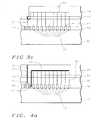
- FIG. 3 ais a representation of a silicon substrate over which an interconnect network is created according to the invention. Power and/or ground pads are provided for external connection.
- the structure that is shown in FIGS. 3 a and 3 brelates to power and ground distribution networks of the invention.
- 66represents one or more than one layer of metal.
- FIG. 3 bfurther distributes the power and ground to the circuit nodes through power and ground distribution lines that are below a layer of passivation and power and ground distribution lines that are above a layer of passivation.
- 66 and 66 ′each represent one or more than one layer of metal.
- FIG. 3 cshows an alternative wherein contact is made to a conventional bond pad through the passivation layer rather than through a post-passivation thick wide metal system.
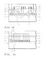
- FIG. 4 ais a representation of a silicon substrate over which an interconnect network is created according to the invention.
- An ESD and/or driver and/or receiver circuit access padis provided through the surface of the layer of dielectric for external connection.
- the structure that is shown in FIGS. 4 a and 4 baddress clock and signal distribution networks of the invention. “Signals” refer to, but are not limited to, address and data. 72 in the figure represents one or more than one layer of metal.
- FIG. 4 bfurther distributes signal and clock to the circuit nodes through clock and signal distribution lines that are below a layer of passivation in addition to clock and signal distribution lines that are above a layer of passivation.
- 71 and 71 ′each represent one or more than one layer of metal.
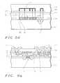
- FIGS. 4 c and 4 dshow smaller intra-chip circuit drivers.
- FIG. 5 ais a representation of a silicon substrate over which an interconnect network is created according to the invention. No I/O connect pad is provided for external connection in specific networks.
- the structure that is shown in FIGS. 5 a and 5 baddresses clock and signal distribution networks of the invention.
- FIG. 5 bdifferentiates between clock and signal distribution lines that are below a layer of passivation and clock and signal distribution lines that are above a layer of passivation.
- FIGS. 5 c and 5 dshow smaller intra-chip circuit drivers.
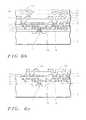
- FIGS. 6 a and 6 bare representations of the interconnect structure of the present invention.
- FIGS. 6 c and 6 dare representations of the interconnect structure of the present invention including wirebonding.
- U.S. Pat. No. 6,383,916teaches an Integrated Circuit structure where re-distribution and interconnect metal layers are created in layers of dielectric over the passivation layer of a conventional Integrated Circuit (IC).
- ICIntegrated Circuit
- a layer of passivationis deposited over the IC, a thick layer of polymer is alternately deposited over the surface of the layer of passivation, and thick, wide metal lines are formed over the passivation.
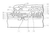
- FIG. 6 athere is shown a cross section of one implementation of U.S. Pat. No. 6,383,916.
- the surface of silicon substrate 10has been provided with transistors 11 and other devices (not shown in FIG. 6 a ).
- the surface of substrate 10is covered by an interlevel dielectric (ILD) layer 12 , formed over the devices.
- ILDinterlevel dielectric
- Layers 14represent all of the metal layers and dielectric layers that are typically created on the dielectric layer 12 .
- Layers 14contain multiple layers of dielectric or insulation and the like; conductive interconnect lines 13 make up the network of electrical connections that are created throughout layers 14 .
- Overlying and on the surface of layers 14are points 16 of electrical contact. These points 16 of electrical contact can, for instance, be bond pads that establish electrical interconnects to external circuits. These points of contact 16 can be points of interconnect within the IC arrangement that establish electrical interconnects to the transistors and other devices in the surface of the substrate.
- a passivation layer 18formed of, for example, a composite layer of silicon oxide and silicon nitride (the thickness of silicon nitride is usually thicker than 0.4 ⁇ m for the passivation purpose), is deposited over the surface of layers 14 , and functions to prevent the penetration of mobile ions (such as sodium ions), moisture, transition metals (such as gold, copper, silver), and other contamination.
- the passivation layeris used to protect the underlying devices (such as transistors, polysilicon resistors, poly-to-poly capacitors, etc.) and the fine-line metal interconnection.
- Lines 24 and 25can be of any design in width and thickness to accommodate specific circuit design requirements.
- This structureallows for the interconnection of circuit elements at various distances using the thick, wide (as compared to the underlying “fine line” metallization in layers 14 ) metal of 25 .
- Thick, wide metal 25has smaller resistance and capacitance than the fine line metal 14 and is also easier and more cost effective to manufacture.
- the thick, wide metalsusually formed by photoresist defined electroplating, are electroplated metals. Gold and copper are preferred.
- a layer of polymer(not shown in FIG. 6 a ) can also be formed to encapsulate the thick, wide metal 25 .
- a second layer of polymer 21is deposited and patterned, followed by the formation of the second layer of thick, wide metal 26 , 27 .
- a final encapsulation 22covers the whole wafer with some exposed pads 28 for connection to external circuits.
- FIGS. 6 c and 6 dare analogous to FIGS. 6 a and 6 b , respectively, but show the process of the invention in conjunction with wirebonding. Openings 29 have been made to aluminum pad 16 .
- Conventional wirebonding techniquesmay be use to form wirebond connections to the original Aluminum pad 16 exposed by openings 29 in FIGS. 6 c and 6 d .
- a piece of aluminum or damascene copperis used for a short distance interconnection between wirebonding pads and the post-passivation interconnection.
- the following commentsrelate to the size and the number of the contact points 16 in FIGS. 6 a - 6 d . Because these contact points 16 are located on top of a thin dielectric (layer 14 , FIGS. 6 a - 6 d ) the pad size cannot be too large since a large pad size brings with it a large capacitance. In addition, a large pad size will interfere with the routing capability of that layer of metal. It is therefore preferred to keep the size of the pad 16 relatively small.
- the size of the contact pad 16can be in the order of 0.5 ⁇ m to 40 ⁇ m, the exact size being dependent on the electrical requirements of the contacts.
- Layer 18 in FIGS. 6 a - 6 dcan be a typical IC passivation layer.
- the most frequently used passivation layer in the present state of the artis plasma enhanced CVD (PECVD) oxide and nitride.
- PECVDplasma enhanced CVD
- a layer of approximately 0.5 ⁇ m PECVD oxidecan be deposited first followed by a layer of approximately more than 0.4 ⁇ m nitride.
- Passivation layer 18is very important because it protects the device wafer from moisture and foreign ion contamination.
- the silicon nitrideis usually thicker than 0.4 ⁇ m.
- this layer between the sub-micron process (of the integrated circuit) and the tens-micron process (of the interconnecting metalization structure)is of critical importance since it allows for a cheaper process that possibly has less stringent clean room requirements for the process of creating the interconnecting metalization structure.
- Layers 20 , 21 , and 22are a thick polymer dielectric layer (for example polyimide) that have a thickness in excess of 2 ⁇ m (after curing).
- the range of the polymer thicknesscan vary from 2 ⁇ m to 150 ⁇ m, dependent on electrical design requirements.
- the Hitachi-Dupont polyimide HD 2732 or 2734 or Asahi polyimide LS800, I-83005, or 8124can, for example, be used.
- the polyimidecan be spin-on coated and cured. After spin-on coating, the polyimide will be cured at 370 degrees C. for 1 hour in a vacuum or nitrogen ambient. For thicker polyimide, the polyimide film can be multiple coated and cured.
- the polyimidealso can be formed by screen printing.
- BCBpolymer benzocyclobutene
- the thick layers 20 , 21 , 22 of polymercan be coated in liquid form on the surface of the layer 18 of passivation or it can be laminated over the surface of layer 18 or passivation by dry film application.
- Additional electrical componentssuch as an inductor, a capacitor, and the like, not shown, can be created on the surface of layer 20 or 22 of polyimide and in electrical contact with underlying metallization.
- FIG. 3 athis figure refers to power and ground architecture.
- a silicon substrate 40over which an interconnect network is created according to the invention, with a wide and thick wire interconnect network created in a thick layer of dielectric overlying a layer of passivation.
- a power and/or ground padcan be provided for external connection.
- FIG. 3 acan be summarized as follows: a silicon substrate 40 is provided in the surface of which there have been created semiconductor devices 42 and at least one electrostatic discharge (ESD) circuit 44 ; a one or more layers 60 of dielectric are deposited over the substrate 40 ; a fine-line interconnect network 61 is created in the dielectric layers 60 making contact with the active circuits 42 and the ESD circuit 44 . A layer of passivation 62 is deposited over the fine-line interconnect network 61 . Openings are created in the layer of passivation 62 that aligns with points of contact in the top layer of the fine-line interconnect network 61 .
- ESDelectrostatic discharge
- a thick layer of dielectric 64is optionally deposited over the layer of passivation 62 ; a wide thick line interconnect network 66 is created in the layer of dielectric 64 , and connected to the ESD circuits.
- a point of electrical contact 68comprising a power or ground contact is provided in the surface of the thick layer 64 of dielectric.
- FIG. 3 bprovides further insight into the creation of the power and ground interconnect lines of the invention whereby these interconnect lines have been shown as interconnect lines 66 and interconnect lines 66 ′.
- Interconnect lines 66have been created above the layer 62 of passivation and act as global power and ground interconnect lines.
- Interconnect lines 66 ′have been created below the layer 62 of passivation and act as local power and ground interconnect lines.
- FIG. 3 cprovides an alternative in which contact is made to a conventional aluminum metal 61 ′, for example, through the passivation layer 62 rather than making contact to the post-passivation thick, wide metal system 66 .
- the top layer of metal 61 ′is used for wirebonding purposes and for connection between wirebonding pads and the wide, thick interconnect lines 66 .
- the distance of 61 ′is a short distance; for example, ⁇ 500 ⁇ m in length.
- the post passivation metallization 66can optionally be performed directly on the passivation layer 62 without the intervening polymer layer.
- the polymer layerprovides distinct advantages, it may be desirable to dispense with the polymer layer in order to save costs.
- FIG. 4 aaddresses the interconnections of signal and clock line.
- Signalhere includes address, data, logic, and analog signals.
- Signalalso includes the power/ground voltage output from voltage regulators.
- FIG. 4 athere is shown a cross section of a silicon substrate 40 over which an interconnect network 61 is created according to the invention.
- An access pad 70 to an ESD circuit 45 or driver or receiver circuits or I/O circuits 45 ′is provided through the layers 64 and 60 of dielectric for external connection. While an ESD circuit 45 is required for all circuits 42 to which an I/O connection is established, the I/O connection can also be provided to a receiver circuit or a driver circuit or an I/O circuit 45 ′.
- a silicon substrate 40is provided; active circuits have been created in the surface of the substrate 40 including an ESD circuit 45 and the receiver, driver and I/O circuit 45 ′.
- First layers 60 of dielectric of inorganic materialare deposited over the substrate 40 and a fine-line interconnect network 61 is created in the layers 60 of dielectric, making contact with the active circuitry 45 , 45 ′, and 42 .
- a layer 62 of passivationis deposited over the first thin layers 60 of dielectric; a pattern 63 of metal plugs is created in the layer 62 of passivation (or, for low aspect ratio openings, direct contact is established between overlying layers 72 of metal through an opening in an interposed layer 64 of dielectric); the metal interconnects 67 align with points of electrical contact in the surface of the first layers 60 of dielectric.
- One or more thicker layers 64 of dielectricare deposited over the surface of the layer 62 of passivation, typically of an organic material; a wide thick line interconnect network 72 is created in the thicker layer 64 of dielectric, making electrical contact with the metal plugs or the metal pads in or under the layer 62 of passivation connected to the receiver, driver or I/O circuit 45 ′.
- a point of electrical contact 70is provided in the surface of the second layer 64 of dielectric and connected to the ESD circuit 45 and the receiver, driver or I/O circuit 45 ′.
- FIG. 4 bprovides further insight into the creation of the signal and clock interconnect lines of the invention whereby these interconnect lines have been shown as interconnect lines 71 and interconnect lines 71 ′.
- Interconnect lines 71have been created above the layer 62 of passivation and act as global signal and clock interconnect lines.
- Interconnect lines 71 ′have been created below the layer 62 of passivation and act as local signal and clock interconnect lines.
- internal circuits 42have no driver, no receiver, and no ESD connections.
- Intra-chip drivers and receivers 80may be necessary if the interconnection distance is long and/or the load of the net of circuits 42 is large, as shown in FIGS. 4 c and 4 d .
- a driver circuitis used to drive a load; i.e., to drive current.
- a driver currentis the output of a driver circuit.
- the ability to drive currentis proportional, in CMOS devices, to the W/L ratio, where W/L is the ratio of the device channel width to its length.
- These intra-chip drivers 80are typically smaller than I/O drivers 45 ′.
- Intra-chip circuits 80typically have no ESD circuits and no I/O circuits. For short distance on-chip interconnection, no intra-chip circuits may be required.
- FIG. 4 cshows an interconnecting structure 72 connecting multiple intra-chip drivers or receivers 80 , which are connected in series to the internal circuits 42 .
- FIG. 4 dshows an example of internal circuits 42 that need to utilize attached intra-chip drivers or receivers while internal circuits 42 ′ do not require attached intra-chip drivers or receivers. Also shown in FIG. 4 d is an interconnecting structure 71 connecting multiple intra-chip drivers or receivers 80 , which are connected in series to the internal circuits 42 .
- Intra-chip circuits 80are usually smaller than the off-chip drivers 45 ′.
- the intra-chip driver circuits 80are different from the off-chip circuits 45 ′ in that they have no I/O circuits and no ESD circuits.
- FIGS. 4 c and 4 dshow smaller internal driver circuits 80 connected to the internal circuits 42 . 45 ′ are larger off-chip circuits.
- FIG. 5 ashows a representation of a silicon substrate 40 over which an interconnect network 74 is created according to the invention, with the interconnect network 74 created in a thick layer 64 of dielectric overlying a layer 62 of passivation. No ESD circuit, receiver, driver or I/O circuit access pad is provided for external connection to the internal circuits 42 . Shown in FIG. 5 a and not previously highlighted is the clock or signal interconnect line 74 , providing for an interconnect scheme of thick, wide lines overlying a passivation layer 62 whereby no external I/O connections are provided.
- each thick, wide interconnect line(where such thick, wide interconnect lines are used) must be provided with at least one I/O connect point for off-chip connection.
- the method that is used to create the wide thick line interconnect lines 74 that is shown in cross section in FIG. 5 acan be summarized as follows and is similar to that described above for FIG. 4 a .
- a silicon substrate 40is provided. Active devices have been provided in the surface of the substrate.
- First thin layers 60 of dielectricare deposited over the surface of the substrate 40 , a fine-line interconnect network 61 is created in the first layers 60 of dielectric, comprising fine-line interconnect lines, making contact with points of electrical contact in the surface of the substrate 40 .
- FIG. 5 ashows a series of driver/receivers, or transceivers, or repeater devices 103 each comprising a receiver 101 and a driver 102 . Receivers 101 are connected to drivers 102 .
- FIG. 5 bprovides further insight into the creation of the signal and clock interconnect lines of the invention whereby these interconnect lines have been shown as interconnect lines 71 and interconnect lines 71 ′.
- Interconnect lines 71have been created above the layer 62 of passivation and can act as global signal and clock interconnect lines.
- Interconnect lines 71 ′have been created below the layer 62 of passivation and act as local signal and clock interconnect lines.
- internal circuits 42are shown. Circuits 42 have no I/O circuits and no ESD circuits.
- FIGS. 5 c and 5 dshow smaller internal driver circuits 80 connected to the internal circuits 42 .
- FIGS. 5 c and 5 dshow an interconnecting structure 74 connects multiple intra-chip drivers or receivers 80 , which are connected in series to the internal circuits 42 .
- FIGS. 3-5show a fine-line interconnect network 61 that underlies the layer 62 of passivation
- the inventionalso enables and can be further extended with the complete elimination of the fine-line interconnect network 61 and creating an interconnect network in the dielectric layer 64 that uses only thick, wide wires.
- the first layer of dielectric 60is not applied, the layer 62 of passivation is deposited directly over the surface of the created semiconductor devices 58 in or on the surface of substrate 40 .
- the post-passivation interconnection of the present inventioncan connect to three types of circuits (i) off-chip drivers, receivers, I/O circuits, and ESD circuits, (ii) intra-chip drivers and receivers, and (iii) internal circuits.
- No driveris required for freeway interconnection with a distance ⁇ “D”.
- a smaller driveris used for freeway interconnection with a distance>“D”; that is, intra-chip connection.
- a large driverlarger than the intra-chip driver, is used for off-chip connection.
Landscapes
- Engineering & Computer Science (AREA)
- Computer Hardware Design (AREA)
- Microelectronics & Electronic Packaging (AREA)
- Power Engineering (AREA)
- Physics & Mathematics (AREA)
- Condensed Matter Physics & Semiconductors (AREA)
- General Physics & Mathematics (AREA)
- Geometry (AREA)
- Internal Circuitry In Semiconductor Integrated Circuit Devices (AREA)
- Semiconductor Integrated Circuits (AREA)
Abstract
Description
- This application is a continuation of application Ser. No. 11/788,221, filed on Apr. 19, 2007, now pending, which is a continuation of application Ser. No. 10/685,872, Oct. 15, 2003, now U.S. Pat. No. 7,230,340.
- 1. Field of the Invention
- The invention relates to the fabrication of integrated circuit devices, and more particularly, to a method of post-passivation processing for the creation of conductive interconnects.
- 2. Description of the Prior Art
- Improvements in semiconductor device performance are typically obtained by scaling down the geometric dimensions of the Integrated Circuits; this results in a decrease in the cost per die while at the same time some aspects of semiconductor device performance are improved. The metal connections which connect the Integrated Circuit to other circuit or system components become of relative more importance and have, with the further miniaturization of the IC, an increasingly negative impact on the circuit performance. The parasitic capacitance and resistance of the metal interconnections increase, which degrades the chip performance significantly. Of most concern in this respect is the voltage drop along the power and ground buses and the RC delay of the critical signal paths. Attempts to reduce the resistance by using wider metal lines result in higher capacitance of these wires.
- To solve this problem, one approach has been to develop low resistance metal (such as copper) for the wires while low-k dielectric materials are used in between signal lines. Current practice is to create metal interconnection networks under a layer of passivation. This approach, however, limits the interconnect network to fine line interconnects and the therewith associated high parasitic capacitance and high line resistivity. The latter two parameters, because of their relatively high values, degrade circuit performance, an effect which becomes even more severe for higher frequency applications and for long interconnect lines that are, for instance, used for clock distribution lines. Also, fine line interconnect metal cannot carry high values of current that is typically needed for ground busses and for power busses.
- It has previously been stated that it is of interest to the semiconductor art to provide a method of creating interconnect lines that removes typical limitations that are imposed on the interconnect wires, such as unwanted parasitic capacitances and high interconnect line resistivity. U.S. Pat. No. 6,383,916 to the same assignee as the present invention provides such a method. An analogy can be drawn in this respect whereby the currently (prior art) used fine-line interconnection schemes, which are created under a layer of passivation, are the streets in a city; in the post-passivation interconnection scheme of the above patent, the interconnections that are created above a layer of passivation can be considered the freeways between cities.
FIG. 1 shows a diagram of a silicon substrate on the surface of which has been created a conductive interconnect network. The structure that is shown inFIG. 1 addresses prior art power and ground distribution networks. The various features that have been highlighted inFIG. 1 are the following:- 40, a silicon substrate on the surface of which has been created an interconnect network
- 42, a sample number of semiconductor circuits that have been created in or on the surface of the
substrate 40 - 44, two electrostatic discharge (ESD) circuits created in or on the surface of the
substrate 40; one ESD circuit is provided for each pad that is accessible for external connections (pads 52, see below) - 46 is a layer of interconnect lines; these interconnect lines are above the surface of
substrate 40 and under thelayer 48 of passivation and represent a typical application of prior art fine-line interconnects; these fine-line interconnects oflayer 46 typically have high resistivity and high parasitic capacitance. - 48 is a layer of passivation that is deposited over the surface of the
layer 46 of interconnect lines. The passivation layer is the final layer of the IC process in the prior art. The passivation layer is used to protect the underlying devices and fine-line interconnection from damage by mobile ions, moisture, transition metals, and contamination. - 50 is a power or ground bus that connects to the
circuits 42 via fine-line interconnect lines provided inlayer 46; this power or ground bus is typically of wider metal since this power or ground bus carries the accumulated current or ground connection for thedevices 42. The power, groun buses are built in the fine line interconnect under the passivation layer. The fine line interconnection can be in one layer or more than one layer of metals. - 52 is a power or ground pad that passes through the
layer 48 of passivation and that has been connected to the power orground bus 50.
- From the above the following can be summarized: circuits are created in or on the surface of a silicon substrate, interconnect lines are created for these circuits for further interconnection to external circuitry, the circuits are, on a per I/O pad basis, provided with an ESD circuit; these circuits with their ESD circuit are connected to a power or ground pad that penetrates a layer of passivation. The layer of passivation is the final layer that overlies the created interconnect line structure; the interconnect lines underneath the layer of passivation are fine line interconnects and have all the electrical disadvantages of fine line interconnects such as high resistivity and high parasitic capacitance.
- Relating to the diagram that is shown in
FIG. 1 , the following comment applies: ESD circuits are, as is known in the art, provided for the protection of semiconductor circuits against unwanted electrostatic discharge. For this reason, each pad that connects a semiconductor circuit to the external circuits must be provided with an ESD circuit. FIG. 2 shows a diagram of a prior art configuration that resembles the diagram shown inFIG. 1 . The structure that is shown inFIG. 2 however relates to clock and signal distribution networks.FIG. 2 shows in addition (to the previously highlighted aspects ofFIG. 1 ):- 45 are two ESD circuits that are provided in or on the surface of the
substrate 40; ESD circuits are always required for any external connection to an input/output (I/O) pad. - 45′ which are circuits that can be receiver or driver or I/O circuits for input (receiver) or output (driver) or I/O purposes respectively.
- 54 is a clock, signal, address, or data bus built in the fine line interconnection metal under the passivation layer. The clock, signal, or buses can be in one layer or in more than one layer of fine line interconnect metals.
- 56 is a clock or signal pad that has been extended through the
layer 48 of passivation.
- 45 are two ESD circuits that are provided in or on the surface of the
- The same comments apply to the diagram that is shown in
FIG. 2 as previously have been made with respect toFIG. 1 , with as a summary statement that the layer of passivation is the final layer that overlies the created structure, the interconnect lines underneath the layer of passivation are fine line interconnects and have all the electrical disadvantages of fine line interconnects such as high resistivity and high parasitic capacitance. - Further with respect to
FIG. 2 wherepads 56 are signal or clock pads: pads 56 must be connected to ESD and driver/receiver or I/O circuits 45- for signal or
clock pads 56, these pads must be connected not only to ESD circuits but also to driver or receiver or I/O circuits, highlighted ascircuit 45′ inFIG. 2 - after (clock and signal) stimuli have passed through the ESD and driver/receiver or I/O circuits, these stimuli are further routed using, under prior art methods, fine-line interconnect wires. A layer of passivation is deposited over the dielectric layer in which the interconnect network has been created.
- It is therefore of interest to the semiconductor art to provide a method of creating interconnect lines that removes typical limitations that are imposed on the interconnect wires, such as unwanted parasitic capacitances and high interconnect line resistivity. The present invention is related to U.S. Pat. No. 6,303,423, to the same assignee as the present invention.
- A principal objective of the invention is to provide a method for the creation of interconnect metal that allows for the use of thick and wide metal.
- Another objective of the invention is to provide a method for the creation of interconnect metal that uses the application of a thick layer of dielectric such as polymer.
- Yet another objective of the invention is to provide a method that allows for the creation of long interconnect lines, whereby these long interconnect lines do not have high resistance or introduce high parasitic capacitance.
- A still further objective of the invention is to create interconnect lines that can carry high levels of current for the creation of power and ground distribution networks.
- A still further objective of the invention is to create interconnect metal that can be created using cost effective methods of manufacturing by creating the interconnect metal on the surface of and after a layer of passivation has been deposited.
- In accordance with the objectives of the invention a new method is provided for the creation of interconnect lines. Fine line interconnects are provided in a first layer of dielectric overlying semiconductor circuits that have been created in or on the surface of a substrate. A layer of passivation is deposited over the layer of dielectric; a thick second layer of dielectric is created over the surface of the layer of passivation. Thick and wide interconnect lines are created in the thick second layer of dielectric. Intra-chip drivers are connected to the thick, wide post-passivation interconnections.
FIG. 1 is a representation of a silicon substrate over which a prior art fine-line interconnect network is created over which a layer of passivation is deposited, and power and/or ground pads are provided through the layer of passivation for external connection. The structure that is shown inFIG. 1 addresses prior art power and ground distribution networks.FIG. 2 is a representation of a silicon substrate over which a prior art fine-line interconnect network is created over which a layer of passivation is deposited, and clock and/or signal pads are provided through the layer of passivation for external connection. The structure that is shown inFIG. 2 addresses prior art clock and signal distribution networks.FIG. 3 ais a representation of a silicon substrate over which an interconnect network is created according to the invention. Power and/or ground pads are provided for external connection. The structure that is shown inFIGS. 3 aand3brelates to power and ground distribution networks of the invention.66 represents one or more than one layer of metal.FIG. 3 bfurther distributes the power and ground to the circuit nodes through power and ground distribution lines that are below a layer of passivation and power and ground distribution lines that are above a layer of passivation.66 and66′ each represent one or more than one layer of metal.FIG. 3 cshows an alternative wherein contact is made to a conventional bond pad through the passivation layer rather than through a post-passivation thick wide metal system.FIG. 4 ais a representation of a silicon substrate over which an interconnect network is created according to the invention. An ESD and/or driver and/or receiver circuit access pad is provided through the surface of the layer of dielectric for external connection. The structure that is shown inFIGS. 4 aand4baddress clock and signal distribution networks of the invention. “Signals” refer to, but are not limited to, address and data.72 in the figure represents one or more than one layer of metal.FIG. 4 bfurther distributes signal and clock to the circuit nodes through clock and signal distribution lines that are below a layer of passivation in addition to clock and signal distribution lines that are above a layer of passivation.71 and71′ each represent one or more than one layer of metal.FIGS. 4 cand4dshow smaller intra-chip circuit drivers.FIG. 5 ais a representation of a silicon substrate over which an interconnect network is created according to the invention. No I/O connect pad is provided for external connection in specific networks. The structure that is shown inFIGS. 5 aand5baddresses clock and signal distribution networks of the invention.FIG. 5 bdifferentiates between clock and signal distribution lines that are below a layer of passivation and clock and signal distribution lines that are above a layer of passivation.FIGS. 5 cand5dshow smaller intra-chip circuit drivers.FIGS. 6 aand6bare representations of the interconnect structure of the present invention.FIGS. 6 cand6dare representations of the interconnect structure of the present invention including wirebonding.- U.S. Pat. No. 6,383,916 teaches an Integrated Circuit structure where re-distribution and interconnect metal layers are created in layers of dielectric over the passivation layer of a conventional Integrated Circuit (IC). A layer of passivation is deposited over the IC, a thick layer of polymer is alternately deposited over the surface of the layer of passivation, and thick, wide metal lines are formed over the passivation.
- Referring now more specifically to
FIG. 6 a, there is shown a cross section of one implementation of U.S. Pat. No. 6,383,916. The surface ofsilicon substrate 10 has been provided withtransistors 11 and other devices (not shown inFIG. 6 a). The surface ofsubstrate 10 is covered by an interlevel dielectric (ILD)layer 12, formed over the devices. - Layers14 (two examples are shown) represent all of the metal layers and dielectric layers that are typically created on the
dielectric layer 12.Layers 14 contain multiple layers of dielectric or insulation and the like;conductive interconnect lines 13 make up the network of electrical connections that are created throughoutlayers 14. Overlying and on the surface oflayers 14 arepoints 16 of electrical contact. Thesepoints 16 of electrical contact can, for instance, be bond pads that establish electrical interconnects to external circuits. These points ofcontact 16 can be points of interconnect within the IC arrangement that establish electrical interconnects to the transistors and other devices in the surface of the substrate. Apassivation layer 18, formed of, for example, a composite layer of silicon oxide and silicon nitride (the thickness of silicon nitride is usually thicker than 0.4 μm for the passivation purpose), is deposited over the surface oflayers 14, and functions to prevent the penetration of mobile ions (such as sodium ions), moisture, transition metals (such as gold, copper, silver), and other contamination. The passivation layer is used to protect the underlying devices (such as transistors, polysilicon resistors, poly-to-poly capacitors, etc.) and the fine-line metal interconnection. - The key steps of U.S. Pat. No. 6,383,916 begin with the deposition of a
thick layer 20 of a polymer, preferably polyimide, that is deposited over the surface ofpassivation layer 18. Access must be provided to points ofelectrical contact 16; for this reason a pattern of openings is formed through thepolyimide layer 20 and thepassivation layer 18. Contact points16 are, by means of the openings that are created in thelayer 20 of polyimide, electrically extended to the surface oflayer 20. - After formation of the openings, metallization is performed to create patterned
wide metal layers Lines wide metal 25 has smaller resistance and capacitance than thefine line metal 14 and is also easier and more cost effective to manufacture. The thick, wide metals, usually formed by photoresist defined electroplating, are electroplated metals. Gold and copper are preferred. Optionally, a layer of polymer (not shown inFIG. 6 a) can also be formed to encapsulate the thick,wide metal 25. - Referring now to
FIG. 6 b, multiple layers of post-passivation metals can also be built for some applications. A second layer ofpolymer 21 is deposited and patterned, followed by the formation of the second layer of thick,wide metal final encapsulation 22 covers the whole wafer with some exposedpads 28 for connection to external circuits. FIGS. 6 cand6dare analogous toFIGS. 6 aand6b, respectively, but show the process of the invention in conjunction with wirebonding.Openings 29 have been made toaluminum pad 16. Conventional wirebonding techniques may be use to form wirebond connections to theoriginal Aluminum pad 16 exposed byopenings 29 inFIGS. 6 cand6d. Here, a piece of aluminum or damascene copper is used for a short distance interconnection between wirebonding pads and the post-passivation interconnection.- The following comments relate to the size and the number of the contact points16 in
FIGS. 6 a-6d. Because these contact points16 are located on top of a thin dielectric (layer 14,FIGS. 6 a-6d) the pad size cannot be too large since a large pad size brings with it a large capacitance. In addition, a large pad size will interfere with the routing capability of that layer of metal. It is therefore preferred to keep the size of thepad 16 relatively small. The size of thecontact pad 16 can be in the order of 0.5 μm to 40 μm, the exact size being dependent on the electrical requirements of the contacts. - The referenced application does not impose a limitation on the number of contact pads that can be included in the design; this number is not only dependent on package design requirements but is mostly dependent on the internal circuit design requirements.
Layer 18 inFIGS. 6 a-6dcan be a typical IC passivation layer. - The most frequently used passivation layer in the present state of the art is plasma enhanced CVD (PECVD) oxide and nitride. In creating
layer 18 of passivation, a layer of approximately 0.5 μm PECVD oxide can be deposited first followed by a layer of approximately more than 0.4 μm nitride.Passivation layer 18 is very important because it protects the device wafer from moisture and foreign ion contamination. To achieve the passivation purpose, the silicon nitride is usually thicker than 0.4 μm. The positioning of this layer between the sub-micron process (of the integrated circuit) and the tens-micron process (of the interconnecting metalization structure) is of critical importance since it allows for a cheaper process that possibly has less stringent clean room requirements for the process of creating the interconnecting metalization structure. Layers - For the deposition of
layers - Another material that can be used to create
layers - The thick layers20,21,22 of polymer can be coated in liquid form on the surface of the
layer 18 of passivation or it can be laminated over the surface oflayer 18 or passivation by dry film application. - Additional electrical components such as an inductor, a capacitor, and the like, not shown, can be created on the surface of
layer - Now, the process of the present invention will be described in detail. Referring now specifically to
FIG. 3 a, this figure refers to power and ground architecture. There is shown inFIG. 3 aasilicon substrate 40 over which an interconnect network is created according to the invention, with a wide and thick wire interconnect network created in a thick layer of dielectric overlying a layer of passivation. A power and/or ground pad can be provided for external connection. Following are the various features that are shown inFIG. 3 a: - 40 is the silicon substrate on the surface of which interconnect lines are created in accordance with the invention.
- 42 are semiconductor circuits that are created in or on the surface of
substrate 40. Each semiconductor circuit has several nodes connected to other circuits or power/ground. - 43 is the power or ground node of the
semiconductorcircuits 42. - 44 is an ESD circuit that is provided for the protection of
circuits 42. - 58 is a layer including the
semiconductor devices 42 that have been created in or on the surface ofsubstrate 40. - 60 are one or more dielectric layers that have been created overlying the
layer 58 including thesemiconductor devices 42. - 61 is a connection comprising metal formed through a via through one or more
dielectric layers 60; more such vias are shown inFIG. 3 abut are, for reasons of simplicity, not highlighted. - 62 is a layer of passivation that has been deposited overlying the
layer 60. - 63 is one of the vias that passes through
layer 62 of passivation; more such vias are shown inFIG. 3 abut are, for reasons of simplicity, not highlighted. - 64 is a layer of dielectric in which, as a post-passivation process, interconnects have been created.
- 65 is a power or ground bus that is connected to the
ESD circuit 44, originating inlayer 64 and further passing throughlayers dielectric layers - 66 is the power or ground bus for the connection scheme in
layer 64. This power orground bus 66 could be one or more than one thick, wide metal layers indielectric layer 64 including a polymer. For multiple layers of metal, the metals are connected through vias in the polymer. - 67 is a via that is created overlying the
layer 62 of passivation and in thedielectric layer 64; more such vias are shown inFIG. 3 abut are, for reasons of simplicity, not highlighted. - 68 is the power or ground pad for the
multiple semiconductor devices 42 inlayer 58.
- From the representation that is shown in
FIG. 3 a, it is clear that, most importantly, the ability to create interconnects tosemiconductor devices 42 that have been created in or on the surface of asubstrate 40 has been extended by creating these interconnects not only as fine-line interconnects61 inlayer 60 but extending the interconnect by creation of a wide, thickwire interconnect network 66 overlying a layer ofpassivation 62. This provides immediate and significant benefits in that these lines are further removed from the surface of the substrate40 (reducing parasitic influences by the interconnect lines on thesemiconductor devices 42 that are created in or on the surface of the substrate40) while theinterconnect network 66 that is created overlying the layer ofpassivation 62 can now contain sturdier; that is, thicker and wider, interconnect lines. The thick,wide metal interconnects 66 can be used for power and ground distribution; this distribution then takes place above a layer ofpassivation 62 and partially replaces and extends the conventional method of having for these purposes a fine-line distribution interconnect network under the layer ofpassivation 62. - Some points of interest can be listed at this time as they relate to prior art methods and to the invention.
- provides an ESD circuit for each pad that is used for external input/output interconnect
- provides a fine-line interconnect network for further distribution of the power and ground stimuli, and
- the fine-line power and ground distribution network is created underneath a layer of passivation.
- In this respect and related to the above provided comments, it must be remembered that power and ground pads do not require drivers and/or receiver circuitry.
- The Invention:
- does not need to create an ESD circuit for each pad that is used for external input/output interconnect, in view of the more robust wiring that is connected to the ESD circuit, resulting in reduced power loss and resulting in more power being delivered to the ESD circuit, and
- allows for the power and ground interconnects to be directly connected to the power and ground nodes of the internal circuits of a semiconductor device, this either without an ESD circuit or with a smaller than regular ESD circuit (as previously explained).
- The method that is used to create the interconnect network that is shown in
FIG. 3 aaddresses only the use of power and ground connections.FIG. 3 acan be summarized as follows: asilicon substrate 40 is provided in the surface of which there have been createdsemiconductor devices 42 and at least one electrostatic discharge (ESD)circuit 44; a one ormore layers 60 of dielectric are deposited over thesubstrate 40; a fine-line interconnect network 61 is created in thedielectric layers 60 making contact with theactive circuits 42 and theESD circuit 44. A layer ofpassivation 62 is deposited over the fine-line interconnect network 61. Openings are created in the layer ofpassivation 62 that aligns with points of contact in the top layer of the fine-line interconnect network 61. A thick layer ofdielectric 64 is optionally deposited over the layer ofpassivation 62; a wide thickline interconnect network 66 is created in the layer ofdielectric 64, and connected to the ESD circuits. A point ofelectrical contact 68 comprising a power or ground contact is provided in the surface of thethick layer 64 of dielectric. FIG. 3 bprovides further insight into the creation of the power and ground interconnect lines of the invention whereby these interconnect lines have been shown asinterconnect lines 66 andinterconnect lines 66′.Interconnect lines 66 have been created above thelayer 62 of passivation and act as global power and ground interconnect lines.Interconnect lines 66′ have been created below thelayer 62 of passivation and act as local power and ground interconnect lines.FIG. 3 cprovides an alternative in which contact is made to aconventional aluminum metal 61′, for example, through thepassivation layer 62 rather than making contact to the post-passivation thick,wide metal system 66. The top layer ofmetal 61′ is used for wirebonding purposes and for connection between wirebonding pads and the wide, thick interconnect lines66. The distance of61′ is a short distance; for example, <500 μm in length.- In the process of the present invention, in all aspects shown in the figures, the
post passivation metallization 66 can optionally be performed directly on thepassivation layer 62 without the intervening polymer layer. Although the polymer layer provides distinct advantages, it may be desirable to dispense with the polymer layer in order to save costs. - Referring now to
FIG. 4 a,FIG. 4 aaddresses the interconnections of signal and clock line. Signal here includes address, data, logic, and analog signals. Signal also includes the power/ground voltage output from voltage regulators. InFIG. 4 athere is shown a cross section of asilicon substrate 40 over which aninterconnect network 61 is created according to the invention. Anaccess pad 70 to anESD circuit 45 or driver or receiver circuits or I/O circuits 45′ is provided through thelayers ESD circuit 45 is required for allcircuits 42 to which an I/O connection is established, the I/O connection can also be provided to a receiver circuit or a driver circuit or an I/O circuit 45′. - The features not previously highlighted that are shown in
FIG. 4 aare: - the invention provides an
interconnect network 72 comprising wide, thick interconnect lines for distribution of the clock and signal stimuli, - the invention creates an
interconnect network 72 of thick, wide interconnect lines for the clock and signal stimuli overlying a layer ofpassivation 62, - 70 is an external connection (pad) that is provided for the
ESD circuit 45 and for driver/receiver/I/O circuit 45′;pad 70 provides external access for clock and signal stimuli tocircuits - 72 is a clock or signal bus that is created in the
dielectric layer 64 using thick, wide wires for interconnect lines; it must be noted that the clock and signalinterconnect line distribution 72 is entirely contained within thelayer 64 without providing an external point of I/O interconnect.
- the invention provides an
- The method that is used to create the interconnect network that is shown in cross section in
FIG. 4 acan be summarized as follows. Asilicon substrate 40 is provided; active circuits have been created in the surface of thesubstrate 40 including anESD circuit 45 and the receiver, driver and I/O circuit 45′. First layers60 of dielectric of inorganic material are deposited over thesubstrate 40 and a fine-line interconnect network 61 is created in thelayers 60 of dielectric, making contact with theactive circuitry layer 62 of passivation is deposited over the firstthin layers 60 of dielectric; apattern 63 of metal plugs is created in thelayer 62 of passivation (or, for low aspect ratio openings, direct contact is established betweenoverlying layers 72 of metal through an opening in an interposedlayer 64 of dielectric); the metal interconnects67 align with points of electrical contact in the surface of thefirst layers 60 of dielectric. One or morethicker layers 64 of dielectric are deposited over the surface of thelayer 62 of passivation, typically of an organic material; a wide thickline interconnect network 72 is created in thethicker layer 64 of dielectric, making electrical contact with the metal plugs or the metal pads in or under thelayer 62 of passivation connected to the receiver, driver or I/O circuit 45′. A point ofelectrical contact 70 is provided in the surface of thesecond layer 64 of dielectric and connected to theESD circuit 45 and the receiver, driver or I/O circuit 45′. FIG. 4 bprovides further insight into the creation of the signal and clock interconnect lines of the invention whereby these interconnect lines have been shown asinterconnect lines 71 andinterconnect lines 71′.Interconnect lines 71 have been created above thelayer 62 of passivation and act as global signal and clock interconnect lines.Interconnect lines 71′ have been created below thelayer 62 of passivation and act as local signal and clock interconnect lines. Furthermore,internal circuits 42 have no driver, no receiver, and no ESD connections.- Intra-chip drivers and
receivers 80 may be necessary if the interconnection distance is long and/or the load of the net ofcircuits 42 is large, as shown inFIGS. 4 cand4d. A driver circuit is used to drive a load; i.e., to drive current. A driver current is the output of a driver circuit. The ability to drive current is proportional, in CMOS devices, to the W/L ratio, where W/L is the ratio of the device channel width to its length. Theseintra-chip drivers 80 are typically smaller than I/O drivers 45′.Intra-chip circuits 80 typically have no ESD circuits and no I/O circuits. For short distance on-chip interconnection, no intra-chip circuits may be required.FIG. 4 cshows an interconnectingstructure 72 connecting multiple intra-chip drivers orreceivers 80, which are connected in series to theinternal circuits 42.FIG. 4 dshows an example ofinternal circuits 42 that need to utilize attached intra-chip drivers or receivers whileinternal circuits 42′ do not require attached intra-chip drivers or receivers. Also shown inFIG. 4 dis an interconnectingstructure 71 connecting multiple intra-chip drivers orreceivers 80, which are connected in series to theinternal circuits 42. - Further provided are:
- 45 are two ESD circuits that are provided in or on the surface of the
substrate 40, as shown inFIGS. 4 a-4d; ESD circuits are always required for any external connection to an input/output (I/O) pad - 45′ which are circuits that can be receiver or driver or I/O circuits for input (receiver) or output (driver) or I/O purposes respectively, as shown in
FIGS. 4 a-4d. These are off-chip drivers or receivers or I/O circuits.
- 45 are two ESD circuits that are provided in or on the surface of the
Intra-chip circuits 80 are usually smaller than the off-chip drivers 45′. Theintra-chip driver circuits 80 are different from the off-chip circuits 45′ in that they have no I/O circuits and no ESD circuits.FIGS. 4 cand4dshow smallerinternal driver circuits 80 connected to theinternal circuits 42.45′ are larger off-chip circuits.FIG. 5 ashows a representation of asilicon substrate 40 over which aninterconnect network 74 is created according to the invention, with theinterconnect network 74 created in athick layer 64 of dielectric overlying alayer 62 of passivation. No ESD circuit, receiver, driver or I/O circuit access pad is provided for external connection to theinternal circuits 42. Shown inFIG. 5 aand not previously highlighted is the clock orsignal interconnect line 74, providing for an interconnect scheme of thick, wide lines overlying apassivation layer 62 whereby no external I/O connections are provided. Due to the thick, wide lines of theinterconnect network 74 that is created overlying apassivation layer 62, the clock and signal distribution can take place entirely within thedielectric layer 64; this as opposed to prior art methods where, for clock and signal distribution lines, each thick, wide interconnect line (where such thick, wide interconnect lines are used) must be provided with at least one I/O connect point for off-chip connection.- The method that is used to create the wide thick
line interconnect lines 74 that is shown in cross section inFIG. 5 acan be summarized as follows and is similar to that described above forFIG. 4 a. Asilicon substrate 40 is provided. Active devices have been provided in the surface of the substrate. Firstthin layers 60 of dielectric are deposited over the surface of thesubstrate 40, a fine-line interconnect network 61 is created in thefirst layers 60 of dielectric, comprising fine-line interconnect lines, making contact with points of electrical contact in the surface of thesubstrate 40. Alayer 62 of passivation is deposited over the surface of thefirst layers 60 of dielectric, a pattern ofconductive interconnects 63 is created in thelayer 62 of passivation and aligns with the points of electrical contact in the surface of thefirst layer 60 of dielectric. One or moresecond layers 65 of dielectric are deposited over the surface of thelayer 62 of passivation, the interconnectingstructure 74 making electrical contact with theconductive interconnects 63 in thelayer 62 of passivation.FIG. 5 ashows a series of driver/receivers, or transceivers, orrepeater devices 103 each comprising areceiver 101 and adriver 102.Receivers 101 are connected todrivers 102. FIG. 5 bprovides further insight into the creation of the signal and clock interconnect lines of the invention whereby these interconnect lines have been shown asinterconnect lines 71 andinterconnect lines 71′.Interconnect lines 71 have been created above thelayer 62 of passivation and can act as global signal and clock interconnect lines.Interconnect lines 71′ have been created below thelayer 62 of passivation and act as local signal and clock interconnect lines. Also as shown inFIG. 5 b,internal circuits 42 are shown.Circuits 42 have no I/O circuits and no ESD circuits.FIGS. 5 cand5dshow smallerinternal driver circuits 80 connected to theinternal circuits 42.FIGS. 5 cand5dshow an interconnectingstructure 74 connects multiple intra-chip drivers orreceivers 80, which are connected in series to theinternal circuits 42.- It must further be emphasized that, where
FIGS. 3-5 show a fine-line interconnect network 61 that underlies thelayer 62 of passivation, the invention also enables and can be further extended with the complete elimination of the fine-line interconnect network 61 and creating an interconnect network in thedielectric layer 64 that uses only thick, wide wires. For this application of the invention, the first layer ofdielectric 60 is not applied, thelayer 62 of passivation is deposited directly over the surface of the createdsemiconductor devices 58 in or on the surface ofsubstrate 40. - It is further of value to briefly discuss the above implemented and addressed distinction between fine-line interconnect lines and wide, thick interconnect lines. The following points apply in this respect:
- the prior art fine line interconnect lines are created underneath a layer of passivation, the wide, thick interconnect lines of the invention are created above a layer of passivation
- the fine-line interconnect lines are typically created in a layer of inorganic dielectric, the thick wide interconnect lines are typically created in a layer of dielectric comprising polymer. This is because an inorganic material cannot be deposited as a thick layer of dielectric because such a layer of dielectric could develop fissures and crack as a result. Although the polymer is preferred, the thick wide interconnect lines could be formed over a conventional passivation layer without the polymer.
- fine-line interconnect metal is typically created using methods of sputter with resist etching or of damascene processes using oxide etch with electroplating after which CMP is applied. Either one of these two approaches cannot create thick metal due to cost considerations or oxide cracking
- thick, wide interconnect lines can be created by first sputtering a thin metal base layer, coating and patterning a thick layer of photoresist, applying a thick layer of metal by electroplating, removing the patterned photoresist and performing metal base etching (of the sputtered thin metal base). This method allows for the creation of a pattern of very thick metal; metal thickness in excess of 1 μm can in this manner be achieved while the thickness of the layer of dielectric in which the thick metal interconnect lines are created can be in excess of 2 μm.
- In summary, the post-passivation interconnection of the present invention can connect to three types of circuits (i) off-chip drivers, receivers, I/O circuits, and ESD circuits, (ii) intra-chip drivers and receivers, and (iii) internal circuits. No driver is required for freeway interconnection with a distance<“D”. A smaller driver is used for freeway interconnection with a distance>“D”; that is, intra-chip connection. For I/O and ESD circuits, a large driver, larger than the intra-chip driver, is used for off-chip connection.
- Although the invention has been described and illustrated with reference to specific illustrative embodiments thereof, it is not intended that the invention be limited to those illustrative embodiments. Those skilled in the art will recognize that variations and modifications can be made without departing from the spirit of the invention. It is therefore intended to include within the invention all such variations and modifications which fall within the scope of the appended claims and equivalents thereof.
Claims (20)
Priority Applications (2)
| Application Number | Priority Date | Filing Date | Title |
|---|---|---|---|
| US12/019,635US7928576B2 (en) | 2003-10-15 | 2008-01-25 | Post passivation interconnection schemes on top of the IC chips |
| US13/071,203US8456013B2 (en) | 2003-10-15 | 2011-03-24 | Post passivation interconnection schemes on top of the IC chips |
Applications Claiming Priority (3)
| Application Number | Priority Date | Filing Date | Title |
|---|---|---|---|
| US10/685,872US7230340B2 (en) | 2000-10-18 | 2003-10-15 | Post passivation interconnection schemes on top of the IC chips |
| US11/788,221US7459790B2 (en) | 2003-10-15 | 2007-04-19 | Post passivation interconnection schemes on top of the IC chips |
| US12/019,635US7928576B2 (en) | 2003-10-15 | 2008-01-25 | Post passivation interconnection schemes on top of the IC chips |
Related Parent Applications (1)
| Application Number | Title | Priority Date | Filing Date |
|---|---|---|---|
| US11/788,221ContinuationUS7459790B2 (en) | 2003-10-15 | 2007-04-19 | Post passivation interconnection schemes on top of the IC chips |
Related Child Applications (1)
| Application Number | Title | Priority Date | Filing Date |
|---|---|---|---|
| US13/071,203ContinuationUS8456013B2 (en) | 2003-10-15 | 2011-03-24 | Post passivation interconnection schemes on top of the IC chips |
Publications (2)
| Publication Number | Publication Date |
|---|---|
| US20080116581A1true US20080116581A1 (en) | 2008-05-22 |
| US7928576B2 US7928576B2 (en) | 2011-04-19 |
Family
ID=38443197
Family Applications (4)
| Application Number | Title | Priority Date | Filing Date |
|---|---|---|---|
| US11/788,221Expired - LifetimeUS7459790B2 (en) | 2003-10-15 | 2007-04-19 | Post passivation interconnection schemes on top of the IC chips |
| US12/019,644Expired - LifetimeUS7498255B2 (en) | 2003-10-15 | 2008-01-25 | Post passivation interconnection schemes on top of the IC chips |
| US12/019,635Expired - LifetimeUS7928576B2 (en) | 2003-10-15 | 2008-01-25 | Post passivation interconnection schemes on top of the IC chips |
| US13/071,203Expired - Fee RelatedUS8456013B2 (en) | 2003-10-15 | 2011-03-24 | Post passivation interconnection schemes on top of the IC chips |
Family Applications Before (2)
| Application Number | Title | Priority Date | Filing Date |
|---|---|---|---|
| US11/788,221Expired - LifetimeUS7459790B2 (en) | 2003-10-15 | 2007-04-19 | Post passivation interconnection schemes on top of the IC chips |
| US12/019,644Expired - LifetimeUS7498255B2 (en) | 2003-10-15 | 2008-01-25 | Post passivation interconnection schemes on top of the IC chips |
Family Applications After (1)
| Application Number | Title | Priority Date | Filing Date |
|---|---|---|---|
| US13/071,203Expired - Fee RelatedUS8456013B2 (en) | 2003-10-15 | 2011-03-24 | Post passivation interconnection schemes on top of the IC chips |
Country Status (1)
| Country | Link |
|---|---|
| US (4) | US7459790B2 (en) |
Families Citing this family (6)
| Publication number | Priority date | Publication date | Assignee | Title |
|---|---|---|---|---|
| US8274160B2 (en) | 2003-08-21 | 2012-09-25 | Intersil Americas Inc. | Active area bonding compatible high current structures |
| US7005369B2 (en)* | 2003-08-21 | 2006-02-28 | Intersil American Inc. | Active area bonding compatible high current structures |
| US7459790B2 (en) | 2003-10-15 | 2008-12-02 | Megica Corporation | Post passivation interconnection schemes on top of the IC chips |
| US20130146345A1 (en)* | 2011-12-12 | 2013-06-13 | Kazuki KAJIHARA | Printed wiring board and method for manufacturing the same |
| KR101983137B1 (en)* | 2013-03-04 | 2019-05-28 | 삼성전기주식회사 | Power inductor and manufacturing method thereof |
| US11233025B2 (en) | 2017-05-31 | 2022-01-25 | Futurewei Technologies, Inc. | Merged power pad for improving integrated circuit power delivery |
Citations (95)
| Publication number | Priority date | Publication date | Assignee | Title |
|---|---|---|---|---|
| US4423547A (en)* | 1981-06-01 | 1984-01-03 | International Business Machines Corporation | Method for forming dense multilevel interconnection metallurgy for semiconductor devices |
| US4618878A (en)* | 1983-06-18 | 1986-10-21 | Kabushiki Kaisha Toshiba | Semiconductor device having a multilayer wiring structure using a polyimide resin |
| US4685998A (en)* | 1984-03-22 | 1987-08-11 | Thomson Components - Mostek Corp. | Process of forming integrated circuits with contact pads in a standard array |
| US4789647A (en)* | 1986-01-08 | 1988-12-06 | U.S. Philips Corporation | Method of manufacturing a semiconductor device, in which a metallization with a thick connection electrode is provided on a semiconductor body |
| US4962058A (en)* | 1989-04-14 | 1990-10-09 | International Business Machines Corporation | Process for fabricating multi-level integrated circuit wiring structure from a single metal deposit |
| US5055907A (en)* | 1989-01-25 | 1991-10-08 | Mosaic, Inc. | Extended integration semiconductor structure with wiring layers |
| US5083187A (en)* | 1990-05-16 | 1992-01-21 | Texas Instruments Incorporated | Integrated circuit device having bumped power supply buses over active surface areas and method of manufacture thereof |
| US5106461A (en)* | 1989-04-04 | 1992-04-21 | Massachusetts Institute Of Technology | High-density, multi-level interconnects, flex circuits, and tape for tab |
| US5108950A (en)* | 1987-11-18 | 1992-04-28 | Casio Computer Co., Ltd. | Method for forming a bump electrode for a semiconductor device |
| US5212403A (en)* | 1990-09-10 | 1993-05-18 | Hitachi, Ltd. | Integrated circuit device having an ic chip mounted on the wiring substrate and having suitable mutual connections between internal circuits |
| US5226232A (en)* | 1990-05-18 | 1993-07-13 | Hewlett-Packard Company | Method for forming a conductive pattern on an integrated circuit |
| US5227012A (en)* | 1990-04-24 | 1993-07-13 | Hightec Mg Ag | Method of manufacturing multi-layer thin film circuits containing integrated thin film resistors |
| US5372967A (en)* | 1992-01-27 | 1994-12-13 | Motorola, Inc. | Method for fabricating a vertical trench inductor |
| US5384488A (en)* | 1992-06-15 | 1995-01-24 | Texas Instruments Incorporated | Configuration and method for positioning semiconductor device bond pads using additional process layers |
| US5416356A (en)* | 1993-09-03 | 1995-05-16 | Motorola, Inc. | Integrated circuit having passive circuit elements |
| US5468984A (en)* | 1994-11-02 | 1995-11-21 | Texas Instruments Incorporated | ESD protection structure using LDMOS diodes with thick copper interconnect |
| US5478773A (en)* | 1994-04-28 | 1995-12-26 | Motorola, Inc. | Method of making an electronic device having an integrated inductor |
| US5501006A (en)* | 1993-09-22 | 1996-03-26 | Motorola, Inc. | Method for connection of signals to an integrated circuit |
| US5532512A (en)* | 1994-10-03 | 1996-07-02 | General Electric Company | Direct stacked and flip chip power semiconductor device structures |
| US5576680A (en)* | 1994-03-01 | 1996-11-19 | Amer-Soi | Structure and fabrication process of inductors on semiconductor chip |
| US5635767A (en)* | 1995-06-02 | 1997-06-03 | Motorola, Inc. | Semiconductor device having built-in high frequency bypass capacitor |
| US5659201A (en)* | 1995-06-05 | 1997-08-19 | Advanced Micro Devices, Inc. | High conductivity interconnection line |
| US5665639A (en)* | 1994-02-23 | 1997-09-09 | Cypress Semiconductor Corp. | Process for manufacturing a semiconductor device bump electrode using a rapid thermal anneal |
| US5665989A (en)* | 1995-01-03 | 1997-09-09 | Lsi Logic | Programmable microsystems in silicon |
| US5686764A (en)* | 1996-03-20 | 1997-11-11 | Lsi Logic Corporation | Flip chip package with reduced number of package layers |
| US5691248A (en)* | 1995-07-26 | 1997-11-25 | International Business Machines Corporation | Methods for precise definition of integrated circuit chip edges |
| US5789303A (en)* | 1994-11-28 | 1998-08-04 | Northern Telecom Limited | Method of adding on chip capacitors to an integrated circuit |
| US5792594A (en)* | 1996-04-01 | 1998-08-11 | Motorola, Inc. | Metallization and termination process for an integrated circuit chip |
| US5834845A (en)* | 1995-09-21 | 1998-11-10 | Advanced Micro Devices, Inc. | Interconnect scheme for integrated circuits |
| US5834844A (en)* | 1995-03-24 | 1998-11-10 | Shinko Electric Industries Co., Ltd. | Semiconductor device having an element with circuit pattern thereon |
| US5854513A (en)* | 1995-07-14 | 1998-12-29 | Lg Electronics Inc. | Semiconductor device having a bump structure and test electrode |
| US5882963A (en)* | 1994-11-24 | 1999-03-16 | Siemens Aktiengesellschaft | Method of manufacturing semiconductor components |
| US5883435A (en)* | 1996-07-25 | 1999-03-16 | International Business Machines Corporation | Personalization structure for semiconductor devices |
| US5884990A (en)* | 1996-08-23 | 1999-03-23 | International Business Machines Corporation | Integrated circuit inductor |
| US5892273A (en)* | 1994-10-03 | 1999-04-06 | Kabushiki Kaisha Toshiba | Semiconductor package integral with semiconductor chip |
| US5929508A (en)* | 1998-05-21 | 1999-07-27 | Harris Corp | Defect gettering by induced stress |
| US5952726A (en)* | 1996-11-12 | 1999-09-14 | Lsi Logic Corporation | Flip chip bump distribution on die |
| US5969424A (en)* | 1997-03-19 | 1999-10-19 | Fujitsu Limited | Semiconductor device with pad structure |
| US5994766A (en)* | 1998-09-21 | 1999-11-30 | Vlsi Technology, Inc. | Flip chip circuit arrangement with redistribution layer that minimizes crosstalk |
| US6008102A (en)* | 1998-04-09 | 1999-12-28 | Motorola, Inc. | Method of forming a three-dimensional integrated inductor |
| US6011314A (en)* | 1999-02-01 | 2000-01-04 | Hewlett-Packard Company | Redistribution layer and under bump material structure for converting periphery conductive pads to an array of solder bumps |
| US6016000A (en)* | 1998-04-22 | 2000-01-18 | Cvc, Inc. | Ultra high-speed chip semiconductor integrated circuit interconnect structure and fabrication method using free-space dielectrics |
| US6020640A (en)* | 1996-12-19 | 2000-02-01 | Texas Instruments Incorporated | Thick plated interconnect and associated auxillary interconnect |
| US6022792A (en)* | 1996-03-13 | 2000-02-08 | Seiko Instruments, Inc. | Semiconductor dicing and assembling method |
| US6030877A (en)* | 1997-10-06 | 2000-02-29 | Industrial Technology Research Institute | Electroless gold plating method for forming inductor structures |
| US6040226A (en)* | 1997-05-27 | 2000-03-21 | General Electric Company | Method for fabricating a thin film inductor |
| US6077726A (en)* | 1998-07-30 | 2000-06-20 | Motorola, Inc. | Method and apparatus for stress relief in solder bump formation on a semiconductor device |
| US6103552A (en)* | 1998-08-10 | 2000-08-15 | Lin; Mou-Shiung | Wafer scale packaging scheme |
| US6144100A (en)* | 1997-06-05 | 2000-11-07 | Texas Instruments Incorporated | Integrated circuit with bonding layer over active circuitry |
| US6146958A (en)* | 1996-10-02 | 2000-11-14 | National Semiconductor Corporation | Methods for making VLSI capacitors and high Q VLSI inductors using metal-filled via plugs |
| US6150257A (en)* | 1998-08-28 | 2000-11-21 | Micron Technology, Inc. | Plasma treatment of an interconnect surface during formation of an interlayer dielectric |
| US6159773A (en)* | 1999-02-12 | 2000-12-12 | Lin; Mou-Shiung | Strain release contact system for integrated circuits |
| US6184143B1 (en)* | 1997-09-08 | 2001-02-06 | Hitachi, Ltd. | Semiconductor integrated circuit device and fabrication process thereof |
| US6187680B1 (en)* | 1998-10-07 | 2001-02-13 | International Business Machines Corporation | Method/structure for creating aluminum wirebound pad on copper BEOL |
| US6200888B1 (en)* | 1999-05-07 | 2001-03-13 | Shinko Electric Industries Co., Ltd. | Method of producing semiconductor device comprising insulation layer having improved resistance and semiconductor device produced thereby |
| US6229221B1 (en)* | 1998-12-04 | 2001-05-08 | U.S. Philips Corporation | Integrated circuit device |
| US6236101B1 (en)* | 1997-11-05 | 2001-05-22 | Texas Instruments Incorporated | Metallization outside protective overcoat for improved capacitors and inductors |
| US6245662B1 (en)* | 1998-07-23 | 2001-06-12 | Applied Materials, Inc. | Method of producing an interconnect structure for an integrated circuit |
| US20010012684A1 (en)* | 2000-01-06 | 2001-08-09 | Tsukasa Hattori | Method of forming interconnect |
| US6272736B1 (en)* | 1998-11-13 | 2001-08-14 | United Microelectronics Corp. | Method for forming a thin-film resistor |
| US6288447B1 (en)* | 1999-01-22 | 2001-09-11 | Mitsubishi Denki Kabushiki Kaisha | Semiconductor device including a plurality of interconnection layers |
| US6303423B1 (en)* | 1998-12-21 | 2001-10-16 | Megic Corporation | Method for forming high performance system-on-chip using post passivation process |
| US20010035452A1 (en)* | 2000-03-24 | 2001-11-01 | Test Howard R. | Wire bonding process for copper-metallized integrated circuits |
| US6313517B1 (en)* | 1995-11-22 | 2001-11-06 | Siemens Aktiengesellshaft | Vertically integrated semiconductor component |
| US20010051426A1 (en)* | 1999-11-22 | 2001-12-13 | Scott K. Pozder | Method for forming a semiconductor device having a mechanically robust pad interface. |
| US20020019882A1 (en)* | 2000-08-09 | 2002-02-14 | Satoshi Soejima | Packet-data processing apparatus |
| US6359328B1 (en)* | 1998-12-31 | 2002-03-19 | Intel Corporation | Methods for making interconnects and diffusion barriers in integrated circuits |
| US6362087B1 (en)* | 2000-05-05 | 2002-03-26 | Aptos Corporation | Method for fabricating a microelectronic fabrication having formed therein a redistribution structure |
| US20020070042A1 (en)* | 1999-12-10 | 2002-06-13 | Hudson Extrusions, Inc. | Conduit and cable construction |
| US6429120B1 (en)* | 2000-01-18 | 2002-08-06 | Micron Technology, Inc. | Methods and apparatus for making integrated-circuit wiring from copper, silver, gold, and other metals |
| US20020109232A1 (en)* | 1998-12-21 | 2002-08-15 | Mou-Shiung Lin | Chip structure and process for forming the same |
| US20020115282A1 (en)* | 1998-12-21 | 2002-08-22 | Mou-Shiung Lin | Chip structure and process for forming the same |
| US6545354B1 (en)* | 1999-02-15 | 2003-04-08 | Casio Computer Co., Ltd. | Semiconductor device having a barrier layer |
| US6560862B1 (en)* | 2001-02-06 | 2003-05-13 | Taiwan Semiconductor Manufacturing Company | Modified pad for copper/low-k |
| US20030102551A1 (en)* | 2000-07-13 | 2003-06-05 | Hidekazu Kikuchi | Semiconductor device and method for manufacturing |
| US6605528B1 (en)* | 2000-10-18 | 2003-08-12 | Megic Corporation | Post passivation metal scheme for high-performance integrated circuit devices |
| US6614091B1 (en)* | 2002-03-13 | 2003-09-02 | Motorola, Inc. | Semiconductor device having a wire bond pad and method therefor |
| US6636139B2 (en)* | 2001-09-10 | 2003-10-21 | Taiwan Semiconductor Manufacturing Company | Structure to reduce the degradation of the Q value of an inductor caused by via resistance |
| US6639299B2 (en)* | 2001-04-17 | 2003-10-28 | Casio Computer Co., Ltd. | Semiconductor device having a chip size package including a passive element |
| US6646347B2 (en)* | 2001-11-30 | 2003-11-11 | Motorola, Inc. | Semiconductor power device and method of formation |
| US6653563B2 (en)* | 2001-03-30 | 2003-11-25 | Intel Corporation | Alternate bump metallurgy bars for power and ground routing |
| US20030218246A1 (en)* | 2002-05-22 | 2003-11-27 | Hirofumi Abe | Semiconductor device passing large electric current |
| US6662753B1 (en)* | 2002-09-11 | 2003-12-16 | Joseph Sporn | Multi-functional animal leash |
| US6680544B2 (en)* | 2001-06-13 | 2004-01-20 | Via Technologies, Inc. | Flip-chip bump arrangement for decreasing impedance |
| US6683380B2 (en)* | 2000-07-07 | 2004-01-27 | Texas Instruments Incorporated | Integrated circuit with bonding layer over active circuitry |
| US20040023450A1 (en)* | 2001-02-08 | 2004-02-05 | Mitsuaki Katagiri | Semiconductor integrated circuit device and its manufacturing method |
| US6707124B2 (en)* | 1992-10-26 | 2004-03-16 | Texas Instruments Incorporated | HID land grid array packaged device having electrical and optical interconnects |
| US6780748B2 (en)* | 2001-12-07 | 2004-08-24 | Hitachi, Ltd. | Method of fabricating a wafer level chip size package utilizing a maskless exposure |
| US6861740B2 (en)* | 2002-04-29 | 2005-03-01 | Via Technologies, Inc. | Flip-chip die and flip-chip package substrate |
| US6943440B2 (en)* | 2003-09-09 | 2005-09-13 | Intel Corporation | Methods of processing thick ILD layers using spray coating or lamination for C4 wafer level thick metal integrated flow |
| US6963136B2 (en)* | 2000-12-18 | 2005-11-08 | Renesas Technology Corporation | Semiconductor integrated circuit device |
| US6995470B2 (en)* | 2000-05-31 | 2006-02-07 | Micron Technology, Inc. | Multilevel copper interconnects with low-k dielectrics and air gaps |
| US7239028B2 (en)* | 2002-08-09 | 2007-07-03 | Oki Electric Industry Co., Ltd. | Semiconductor device with signal line having decreased characteristic impedance |
| US7385835B2 (en)* | 1992-04-08 | 2008-06-10 | Elm Technology Corporation | Membrane 3D IC fabrication |
| US7420276B2 (en)* | 1998-12-21 | 2008-09-02 | Megica Corporation | Post passivation structure for semiconductor chip or wafer |
Family Cites Families (19)
| Publication number | Priority date | Publication date | Assignee | Title |
|---|---|---|---|---|
| US5028983A (en) | 1988-10-28 | 1991-07-02 | International Business Machines Corporation | Multilevel integrated circuit packaging structures |
| US6040604A (en)* | 1997-07-21 | 2000-03-21 | Motorola, Inc. | Semiconductor component comprising an electrostatic-discharge protection device |
| US6051879A (en) | 1997-12-16 | 2000-04-18 | Micron Technology, Inc. | Electrical interconnection for attachment to a substrate |
| TW511243B (en) | 2001-12-14 | 2002-11-21 | Megic Corp | Chip structure and process for making the same |
| US7230340B2 (en) | 2000-10-18 | 2007-06-12 | Megica Corporation | Post passivation interconnection schemes on top of the IC chips |
| US8178435B2 (en) | 1998-12-21 | 2012-05-15 | Megica Corporation | High performance system-on-chip inductor using post passivation process |
| US8021976B2 (en) | 2002-10-15 | 2011-09-20 | Megica Corporation | Method of wire bonding over active area of a semiconductor circuit |
| TW519707B (en) | 2001-12-13 | 2003-02-01 | Megic Corp | Chip structure with passivation layer having outer layer connection and its manufacturing process |
| US6383916B1 (en) | 1998-12-21 | 2002-05-07 | M. S. Lin | Top layers of metal for high performance IC's |
| JP3530761B2 (en) | 1999-01-18 | 2004-05-24 | 新光電気工業株式会社 | Semiconductor device |
| FR2791470B1 (en) | 1999-03-23 | 2001-06-01 | Memscap | MONOLITHIC INTEGRATED CIRCUIT INCORPORATING AN INDUCTIVE COMPONENT AND METHOD FOR MANUFACTURING SUCH AN INTEGRATED CIRCUIT |
| US6544880B1 (en) | 1999-06-14 | 2003-04-08 | Micron Technology, Inc. | Method of improving copper interconnects of semiconductor devices for bonding |
| US6500694B1 (en) | 2000-03-22 | 2002-12-31 | Ziptronix, Inc. | Three dimensional device integration method and integrated device |
| US6465879B1 (en) | 1999-10-19 | 2002-10-15 | Citizen Watch Co., Ltd. | Structure for mounting semiconductor device, method of mounting same, semiconductor device, and method of fabricating same |
| JP3287346B2 (en) | 1999-11-29 | 2002-06-04 | カシオ計算機株式会社 | Semiconductor device |
| US6847066B2 (en) | 2000-08-11 | 2005-01-25 | Oki Electric Industry Co., Ltd. | Semiconductor device |
| US7271489B2 (en)* | 2003-10-15 | 2007-09-18 | Megica Corporation | Post passivation interconnection schemes on top of the IC chips |
| US6894399B2 (en) | 2001-04-30 | 2005-05-17 | Intel Corporation | Microelectronic device having signal distribution functionality on an interfacial layer thereof |
| US7459790B2 (en) | 2003-10-15 | 2008-12-02 | Megica Corporation | Post passivation interconnection schemes on top of the IC chips |
- 2007
- 2007-04-19USUS11/788,221patent/US7459790B2/ennot_activeExpired - Lifetime
- 2008
- 2008-01-25USUS12/019,644patent/US7498255B2/ennot_activeExpired - Lifetime
- 2008-01-25USUS12/019,635patent/US7928576B2/ennot_activeExpired - Lifetime
- 2011
- 2011-03-24USUS13/071,203patent/US8456013B2/ennot_activeExpired - Fee Related
Patent Citations (99)
| Publication number | Priority date | Publication date | Assignee | Title |
|---|---|---|---|---|
| US4423547A (en)* | 1981-06-01 | 1984-01-03 | International Business Machines Corporation | Method for forming dense multilevel interconnection metallurgy for semiconductor devices |
| US4618878A (en)* | 1983-06-18 | 1986-10-21 | Kabushiki Kaisha Toshiba | Semiconductor device having a multilayer wiring structure using a polyimide resin |
| US4685998A (en)* | 1984-03-22 | 1987-08-11 | Thomson Components - Mostek Corp. | Process of forming integrated circuits with contact pads in a standard array |
| US4789647A (en)* | 1986-01-08 | 1988-12-06 | U.S. Philips Corporation | Method of manufacturing a semiconductor device, in which a metallization with a thick connection electrode is provided on a semiconductor body |
| US5108950A (en)* | 1987-11-18 | 1992-04-28 | Casio Computer Co., Ltd. | Method for forming a bump electrode for a semiconductor device |
| US5055907A (en)* | 1989-01-25 | 1991-10-08 | Mosaic, Inc. | Extended integration semiconductor structure with wiring layers |
| US5106461A (en)* | 1989-04-04 | 1992-04-21 | Massachusetts Institute Of Technology | High-density, multi-level interconnects, flex circuits, and tape for tab |
| US4962058A (en)* | 1989-04-14 | 1990-10-09 | International Business Machines Corporation | Process for fabricating multi-level integrated circuit wiring structure from a single metal deposit |
| US5227012A (en)* | 1990-04-24 | 1993-07-13 | Hightec Mg Ag | Method of manufacturing multi-layer thin film circuits containing integrated thin film resistors |
| US5083187A (en)* | 1990-05-16 | 1992-01-21 | Texas Instruments Incorporated | Integrated circuit device having bumped power supply buses over active surface areas and method of manufacture thereof |
| US5226232A (en)* | 1990-05-18 | 1993-07-13 | Hewlett-Packard Company | Method for forming a conductive pattern on an integrated circuit |
| US5212403A (en)* | 1990-09-10 | 1993-05-18 | Hitachi, Ltd. | Integrated circuit device having an ic chip mounted on the wiring substrate and having suitable mutual connections between internal circuits |
| US5372967A (en)* | 1992-01-27 | 1994-12-13 | Motorola, Inc. | Method for fabricating a vertical trench inductor |
| US7385835B2 (en)* | 1992-04-08 | 2008-06-10 | Elm Technology Corporation | Membrane 3D IC fabrication |
| US5384488A (en)* | 1992-06-15 | 1995-01-24 | Texas Instruments Incorporated | Configuration and method for positioning semiconductor device bond pads using additional process layers |
| US6707124B2 (en)* | 1992-10-26 | 2004-03-16 | Texas Instruments Incorporated | HID land grid array packaged device having electrical and optical interconnects |
| US5416356A (en)* | 1993-09-03 | 1995-05-16 | Motorola, Inc. | Integrated circuit having passive circuit elements |
| US5501006A (en)* | 1993-09-22 | 1996-03-26 | Motorola, Inc. | Method for connection of signals to an integrated circuit |
| US5665639A (en)* | 1994-02-23 | 1997-09-09 | Cypress Semiconductor Corp. | Process for manufacturing a semiconductor device bump electrode using a rapid thermal anneal |
| US5576680A (en)* | 1994-03-01 | 1996-11-19 | Amer-Soi | Structure and fabrication process of inductors on semiconductor chip |
| US5478773A (en)* | 1994-04-28 | 1995-12-26 | Motorola, Inc. | Method of making an electronic device having an integrated inductor |
| US5532512A (en)* | 1994-10-03 | 1996-07-02 | General Electric Company | Direct stacked and flip chip power semiconductor device structures |
| US5892273A (en)* | 1994-10-03 | 1999-04-06 | Kabushiki Kaisha Toshiba | Semiconductor package integral with semiconductor chip |
| US5468984A (en)* | 1994-11-02 | 1995-11-21 | Texas Instruments Incorporated | ESD protection structure using LDMOS diodes with thick copper interconnect |
| US5882963A (en)* | 1994-11-24 | 1999-03-16 | Siemens Aktiengesellschaft | Method of manufacturing semiconductor components |
| US5789303A (en)* | 1994-11-28 | 1998-08-04 | Northern Telecom Limited | Method of adding on chip capacitors to an integrated circuit |
| US5665989A (en)* | 1995-01-03 | 1997-09-09 | Lsi Logic | Programmable microsystems in silicon |
| US5834844A (en)* | 1995-03-24 | 1998-11-10 | Shinko Electric Industries Co., Ltd. | Semiconductor device having an element with circuit pattern thereon |
| US5635767A (en)* | 1995-06-02 | 1997-06-03 | Motorola, Inc. | Semiconductor device having built-in high frequency bypass capacitor |
| US5659201A (en)* | 1995-06-05 | 1997-08-19 | Advanced Micro Devices, Inc. | High conductivity interconnection line |
| US5854513A (en)* | 1995-07-14 | 1998-12-29 | Lg Electronics Inc. | Semiconductor device having a bump structure and test electrode |
| US5691248A (en)* | 1995-07-26 | 1997-11-25 | International Business Machines Corporation | Methods for precise definition of integrated circuit chip edges |
| US5834845A (en)* | 1995-09-21 | 1998-11-10 | Advanced Micro Devices, Inc. | Interconnect scheme for integrated circuits |
| US6313517B1 (en)* | 1995-11-22 | 2001-11-06 | Siemens Aktiengesellshaft | Vertically integrated semiconductor component |
| US6022792A (en)* | 1996-03-13 | 2000-02-08 | Seiko Instruments, Inc. | Semiconductor dicing and assembling method |
| US5686764A (en)* | 1996-03-20 | 1997-11-11 | Lsi Logic Corporation | Flip chip package with reduced number of package layers |
| US5792594A (en)* | 1996-04-01 | 1998-08-11 | Motorola, Inc. | Metallization and termination process for an integrated circuit chip |
| US5883435A (en)* | 1996-07-25 | 1999-03-16 | International Business Machines Corporation | Personalization structure for semiconductor devices |
| US5884990A (en)* | 1996-08-23 | 1999-03-23 | International Business Machines Corporation | Integrated circuit inductor |
| US6146958A (en)* | 1996-10-02 | 2000-11-14 | National Semiconductor Corporation | Methods for making VLSI capacitors and high Q VLSI inductors using metal-filled via plugs |
| US5952726A (en)* | 1996-11-12 | 1999-09-14 | Lsi Logic Corporation | Flip chip bump distribution on die |
| US6020640A (en)* | 1996-12-19 | 2000-02-01 | Texas Instruments Incorporated | Thick plated interconnect and associated auxillary interconnect |
| US5969424A (en)* | 1997-03-19 | 1999-10-19 | Fujitsu Limited | Semiconductor device with pad structure |
| US6232147B1 (en)* | 1997-03-19 | 2001-05-15 | Fujitsu Limited | Method for manufacturing semiconductor device with pad structure |
| US6040226A (en)* | 1997-05-27 | 2000-03-21 | General Electric Company | Method for fabricating a thin film inductor |
| US6144100A (en)* | 1997-06-05 | 2000-11-07 | Texas Instruments Incorporated | Integrated circuit with bonding layer over active circuitry |
| US6184143B1 (en)* | 1997-09-08 | 2001-02-06 | Hitachi, Ltd. | Semiconductor integrated circuit device and fabrication process thereof |
| US6030877A (en)* | 1997-10-06 | 2000-02-29 | Industrial Technology Research Institute | Electroless gold plating method for forming inductor structures |
| US6236101B1 (en)* | 1997-11-05 | 2001-05-22 | Texas Instruments Incorporated | Metallization outside protective overcoat for improved capacitors and inductors |
| US6008102A (en)* | 1998-04-09 | 1999-12-28 | Motorola, Inc. | Method of forming a three-dimensional integrated inductor |
| US6016000A (en)* | 1998-04-22 | 2000-01-18 | Cvc, Inc. | Ultra high-speed chip semiconductor integrated circuit interconnect structure and fabrication method using free-space dielectrics |
| US5929508A (en)* | 1998-05-21 | 1999-07-27 | Harris Corp | Defect gettering by induced stress |
| US6245662B1 (en)* | 1998-07-23 | 2001-06-12 | Applied Materials, Inc. | Method of producing an interconnect structure for an integrated circuit |
| US6077726A (en)* | 1998-07-30 | 2000-06-20 | Motorola, Inc. | Method and apparatus for stress relief in solder bump formation on a semiconductor device |
| US6103552A (en)* | 1998-08-10 | 2000-08-15 | Lin; Mou-Shiung | Wafer scale packaging scheme |
| US6150257A (en)* | 1998-08-28 | 2000-11-21 | Micron Technology, Inc. | Plasma treatment of an interconnect surface during formation of an interlayer dielectric |
| US5994766A (en)* | 1998-09-21 | 1999-11-30 | Vlsi Technology, Inc. | Flip chip circuit arrangement with redistribution layer that minimizes crosstalk |
| US6187680B1 (en)* | 1998-10-07 | 2001-02-13 | International Business Machines Corporation | Method/structure for creating aluminum wirebound pad on copper BEOL |
| US6272736B1 (en)* | 1998-11-13 | 2001-08-14 | United Microelectronics Corp. | Method for forming a thin-film resistor |
| US6229221B1 (en)* | 1998-12-04 | 2001-05-08 | U.S. Philips Corporation | Integrated circuit device |
| US20020115282A1 (en)* | 1998-12-21 | 2002-08-22 | Mou-Shiung Lin | Chip structure and process for forming the same |
| US6762115B2 (en)* | 1998-12-21 | 2004-07-13 | Megic Corporation | Chip structure and process for forming the same |
| US6303423B1 (en)* | 1998-12-21 | 2001-10-16 | Megic Corporation | Method for forming high performance system-on-chip using post passivation process |
| US7420276B2 (en)* | 1998-12-21 | 2008-09-02 | Megica Corporation | Post passivation structure for semiconductor chip or wafer |
| US6756295B2 (en)* | 1998-12-21 | 2004-06-29 | Megic Corporation | Chip structure and process for forming the same |
| US6455885B1 (en)* | 1998-12-21 | 2002-09-24 | Megic Corporation | Inductor structure for high performance system-on-chip using post passivation process |
| US20020109232A1 (en)* | 1998-12-21 | 2002-08-15 | Mou-Shiung Lin | Chip structure and process for forming the same |
| US6359328B1 (en)* | 1998-12-31 | 2002-03-19 | Intel Corporation | Methods for making interconnects and diffusion barriers in integrated circuits |
| US6288447B1 (en)* | 1999-01-22 | 2001-09-11 | Mitsubishi Denki Kabushiki Kaisha | Semiconductor device including a plurality of interconnection layers |
| US6011314A (en)* | 1999-02-01 | 2000-01-04 | Hewlett-Packard Company | Redistribution layer and under bump material structure for converting periphery conductive pads to an array of solder bumps |
| US6159773A (en)* | 1999-02-12 | 2000-12-12 | Lin; Mou-Shiung | Strain release contact system for integrated circuits |
| US6545354B1 (en)* | 1999-02-15 | 2003-04-08 | Casio Computer Co., Ltd. | Semiconductor device having a barrier layer |
| US6200888B1 (en)* | 1999-05-07 | 2001-03-13 | Shinko Electric Industries Co., Ltd. | Method of producing semiconductor device comprising insulation layer having improved resistance and semiconductor device produced thereby |
| US20010051426A1 (en)* | 1999-11-22 | 2001-12-13 | Scott K. Pozder | Method for forming a semiconductor device having a mechanically robust pad interface. |
| US20020070042A1 (en)* | 1999-12-10 | 2002-06-13 | Hudson Extrusions, Inc. | Conduit and cable construction |
| US20010012684A1 (en)* | 2000-01-06 | 2001-08-09 | Tsukasa Hattori | Method of forming interconnect |
| US6429120B1 (en)* | 2000-01-18 | 2002-08-06 | Micron Technology, Inc. | Methods and apparatus for making integrated-circuit wiring from copper, silver, gold, and other metals |
| US20010035452A1 (en)* | 2000-03-24 | 2001-11-01 | Test Howard R. | Wire bonding process for copper-metallized integrated circuits |
| US6362087B1 (en)* | 2000-05-05 | 2002-03-26 | Aptos Corporation | Method for fabricating a microelectronic fabrication having formed therein a redistribution structure |
| US6995470B2 (en)* | 2000-05-31 | 2006-02-07 | Micron Technology, Inc. | Multilevel copper interconnects with low-k dielectrics and air gaps |
| US6683380B2 (en)* | 2000-07-07 | 2004-01-27 | Texas Instruments Incorporated | Integrated circuit with bonding layer over active circuitry |
| US20030102551A1 (en)* | 2000-07-13 | 2003-06-05 | Hidekazu Kikuchi | Semiconductor device and method for manufacturing |
| US20020019882A1 (en)* | 2000-08-09 | 2002-02-14 | Satoshi Soejima | Packet-data processing apparatus |
| US6605528B1 (en)* | 2000-10-18 | 2003-08-12 | Megic Corporation | Post passivation metal scheme for high-performance integrated circuit devices |
| US6963136B2 (en)* | 2000-12-18 | 2005-11-08 | Renesas Technology Corporation | Semiconductor integrated circuit device |
| US6560862B1 (en)* | 2001-02-06 | 2003-05-13 | Taiwan Semiconductor Manufacturing Company | Modified pad for copper/low-k |
| US20040023450A1 (en)* | 2001-02-08 | 2004-02-05 | Mitsuaki Katagiri | Semiconductor integrated circuit device and its manufacturing method |
| US6653563B2 (en)* | 2001-03-30 | 2003-11-25 | Intel Corporation | Alternate bump metallurgy bars for power and ground routing |
| US6639299B2 (en)* | 2001-04-17 | 2003-10-28 | Casio Computer Co., Ltd. | Semiconductor device having a chip size package including a passive element |
| US6680544B2 (en)* | 2001-06-13 | 2004-01-20 | Via Technologies, Inc. | Flip-chip bump arrangement for decreasing impedance |
| US6636139B2 (en)* | 2001-09-10 | 2003-10-21 | Taiwan Semiconductor Manufacturing Company | Structure to reduce the degradation of the Q value of an inductor caused by via resistance |
| US6646347B2 (en)* | 2001-11-30 | 2003-11-11 | Motorola, Inc. | Semiconductor power device and method of formation |
| US6780748B2 (en)* | 2001-12-07 | 2004-08-24 | Hitachi, Ltd. | Method of fabricating a wafer level chip size package utilizing a maskless exposure |
| US6614091B1 (en)* | 2002-03-13 | 2003-09-02 | Motorola, Inc. | Semiconductor device having a wire bond pad and method therefor |
| US6861740B2 (en)* | 2002-04-29 | 2005-03-01 | Via Technologies, Inc. | Flip-chip die and flip-chip package substrate |
| US20030218246A1 (en)* | 2002-05-22 | 2003-11-27 | Hirofumi Abe | Semiconductor device passing large electric current |
| US7239028B2 (en)* | 2002-08-09 | 2007-07-03 | Oki Electric Industry Co., Ltd. | Semiconductor device with signal line having decreased characteristic impedance |
| US6662753B1 (en)* | 2002-09-11 | 2003-12-16 | Joseph Sporn | Multi-functional animal leash |
| US6943440B2 (en)* | 2003-09-09 | 2005-09-13 | Intel Corporation | Methods of processing thick ILD layers using spray coating or lamination for C4 wafer level thick metal integrated flow |
Also Published As
| Publication number | Publication date |
|---|---|
| US20070200244A1 (en) | 2007-08-30 |
| US20080138978A1 (en) | 2008-06-12 |
| US7928576B2 (en) | 2011-04-19 |
| US8456013B2 (en) | 2013-06-04 |
| US20110175227A1 (en) | 2011-07-21 |
| US7498255B2 (en) | 2009-03-03 |
| US7459790B2 (en) | 2008-12-02 |
Similar Documents
| Publication | Publication Date | Title |
|---|---|---|
| US8013449B2 (en) | Post passivation interconnection schemes on top of the IC chips | |
| US7230340B2 (en) | Post passivation interconnection schemes on top of the IC chips | |
| US7265047B2 (en) | Post passivation interconnection schemes on top of the IC chips | |
| US7372161B2 (en) | Post passivation interconnection schemes on top of the IC chips | |
| US8456013B2 (en) | Post passivation interconnection schemes on top of the IC chips | |
| US7880304B2 (en) | Post passivation interconnection schemes on top of the IC chips |
Legal Events
| Date | Code | Title | Description |
|---|---|---|---|
| AS | Assignment | Owner name:MEGICA CORPORATION, TAIWAN Free format text:ASSIGNMENT OF ASSIGNORS INTEREST;ASSIGNOR:LIN, MOU-SHIUNG;REEL/FRAME:020412/0689 Effective date:20080122 | |
| FEPP | Fee payment procedure | Free format text:PAYOR NUMBER ASSIGNED (ORIGINAL EVENT CODE: ASPN); ENTITY STATUS OF PATENT OWNER: LARGE ENTITY | |
| STCF | Information on status: patent grant | Free format text:PATENTED CASE | |
| AS | Assignment | Owner name:MEGIT ACQUISITION CORP., CALIFORNIA Free format text:MERGER;ASSIGNOR:MEGICA CORPORATION;REEL/FRAME:031283/0198 Effective date:20130611 | |
| AS | Assignment | Owner name:QUALCOMM INCORPORATED, CALIFORNIA Free format text:ASSIGNMENT OF ASSIGNORS INTEREST;ASSIGNOR:MEGIT ACQUISITION CORP.;REEL/FRAME:033303/0124 Effective date:20140709 | |
| FPAY | Fee payment | Year of fee payment:4 | |
| MAFP | Maintenance fee payment | Free format text:PAYMENT OF MAINTENANCE FEE, 8TH YEAR, LARGE ENTITY (ORIGINAL EVENT CODE: M1552); ENTITY STATUS OF PATENT OWNER: LARGE ENTITY Year of fee payment:8 | |
| MAFP | Maintenance fee payment | Free format text:PAYMENT OF MAINTENANCE FEE, 12TH YEAR, LARGE ENTITY (ORIGINAL EVENT CODE: M1553); ENTITY STATUS OF PATENT OWNER: LARGE ENTITY Year of fee payment:12 |