US20080110019A1 - Probe card and method for constructing same - Google Patents
Probe card and method for constructing sameDownload PDFInfo
- Publication number
- US20080110019A1 US20080110019A1US12/008,483US848308AUS2008110019A1US 20080110019 A1US20080110019 A1US 20080110019A1US 848308 AUS848308 AUS 848308AUS 2008110019 A1US2008110019 A1US 2008110019A1
- Authority
- US
- United States
- Prior art keywords
- wafer
- substrate
- probe
- forming
- probes
- Prior art date
- Legal status (The legal status is an assumption and is not a legal conclusion. Google has not performed a legal analysis and makes no representation as to the accuracy of the status listed.)
- Granted
Links
Images


Classifications
- G—PHYSICS
- G01—MEASURING; TESTING
- G01R—MEASURING ELECTRIC VARIABLES; MEASURING MAGNETIC VARIABLES
- G01R1/00—Details of instruments or arrangements of the types included in groups G01R5/00 - G01R13/00 and G01R31/00
- G01R1/02—General constructional details
- G01R1/06—Measuring leads; Measuring probes
- G01R1/067—Measuring probes
- G01R1/073—Multiple probes
- G01R1/07307—Multiple probes with individual probe elements, e.g. needles, cantilever beams or bump contacts, fixed in relation to each other, e.g. bed of nails fixture or probe card
- G01R1/07314—Multiple probes with individual probe elements, e.g. needles, cantilever beams or bump contacts, fixed in relation to each other, e.g. bed of nails fixture or probe card the body of the probe being perpendicular to test object, e.g. bed of nails or probe with bump contacts on a rigid support
- G—PHYSICS
- G01—MEASURING; TESTING
- G01R—MEASURING ELECTRIC VARIABLES; MEASURING MAGNETIC VARIABLES
- G01R1/00—Details of instruments or arrangements of the types included in groups G01R5/00 - G01R13/00 and G01R31/00
- G01R1/02—General constructional details
- G01R1/06—Measuring leads; Measuring probes
- G01R1/067—Measuring probes
- G01R1/073—Multiple probes
- G01R1/07307—Multiple probes with individual probe elements, e.g. needles, cantilever beams or bump contacts, fixed in relation to each other, e.g. bed of nails fixture or probe card
- G01R1/0735—Multiple probes with individual probe elements, e.g. needles, cantilever beams or bump contacts, fixed in relation to each other, e.g. bed of nails fixture or probe card arranged on a flexible frame or film
- G—PHYSICS
- G01—MEASURING; TESTING
- G01R—MEASURING ELECTRIC VARIABLES; MEASURING MAGNETIC VARIABLES
- G01R1/00—Details of instruments or arrangements of the types included in groups G01R5/00 - G01R13/00 and G01R31/00
- G01R1/02—General constructional details
- G01R1/06—Measuring leads; Measuring probes
- G01R1/067—Measuring probes
- G01R1/073—Multiple probes
- G01R1/07307—Multiple probes with individual probe elements, e.g. needles, cantilever beams or bump contacts, fixed in relation to each other, e.g. bed of nails fixture or probe card
- G01R1/07364—Multiple probes with individual probe elements, e.g. needles, cantilever beams or bump contacts, fixed in relation to each other, e.g. bed of nails fixture or probe card with provisions for altering position, number or connection of probe tips; Adapting to differences in pitch
- G01R1/07371—Multiple probes with individual probe elements, e.g. needles, cantilever beams or bump contacts, fixed in relation to each other, e.g. bed of nails fixture or probe card with provisions for altering position, number or connection of probe tips; Adapting to differences in pitch using an intermediate card or back card with apertures through which the probes pass
- Y—GENERAL TAGGING OF NEW TECHNOLOGICAL DEVELOPMENTS; GENERAL TAGGING OF CROSS-SECTIONAL TECHNOLOGIES SPANNING OVER SEVERAL SECTIONS OF THE IPC; TECHNICAL SUBJECTS COVERED BY FORMER USPC CROSS-REFERENCE ART COLLECTIONS [XRACs] AND DIGESTS
- Y10—TECHNICAL SUBJECTS COVERED BY FORMER USPC
- Y10T—TECHNICAL SUBJECTS COVERED BY FORMER US CLASSIFICATION
- Y10T29/00—Metal working
- Y10T29/49—Method of mechanical manufacture
- Y10T29/49002—Electrical device making
- Y10T29/49117—Conductor or circuit manufacturing
- Y10T29/49124—On flat or curved insulated base, e.g., printed circuit, etc.
- Y10T29/4913—Assembling to base an electrical component, e.g., capacitor, etc.
- Y—GENERAL TAGGING OF NEW TECHNOLOGICAL DEVELOPMENTS; GENERAL TAGGING OF CROSS-SECTIONAL TECHNOLOGIES SPANNING OVER SEVERAL SECTIONS OF THE IPC; TECHNICAL SUBJECTS COVERED BY FORMER USPC CROSS-REFERENCE ART COLLECTIONS [XRACs] AND DIGESTS
- Y10—TECHNICAL SUBJECTS COVERED BY FORMER USPC
- Y10T—TECHNICAL SUBJECTS COVERED BY FORMER US CLASSIFICATION
- Y10T29/00—Metal working
- Y10T29/49—Method of mechanical manufacture
- Y10T29/49002—Electrical device making
- Y10T29/49117—Conductor or circuit manufacturing
- Y10T29/49124—On flat or curved insulated base, e.g., printed circuit, etc.
- Y10T29/49147—Assembling terminal to base
- Y10T29/49151—Assembling terminal to base by deforming or shaping
- Y10T29/49153—Assembling terminal to base by deforming or shaping with shaping or forcing terminal into base aperture
- Y—GENERAL TAGGING OF NEW TECHNOLOGICAL DEVELOPMENTS; GENERAL TAGGING OF CROSS-SECTIONAL TECHNOLOGIES SPANNING OVER SEVERAL SECTIONS OF THE IPC; TECHNICAL SUBJECTS COVERED BY FORMER USPC CROSS-REFERENCE ART COLLECTIONS [XRACs] AND DIGESTS
- Y10—TECHNICAL SUBJECTS COVERED BY FORMER USPC
- Y10T—TECHNICAL SUBJECTS COVERED BY FORMER US CLASSIFICATION
- Y10T29/00—Metal working
- Y10T29/49—Method of mechanical manufacture
- Y10T29/49002—Electrical device making
- Y10T29/49117—Conductor or circuit manufacturing
- Y10T29/49124—On flat or curved insulated base, e.g., printed circuit, etc.
- Y10T29/49155—Manufacturing circuit on or in base
Definitions
- the present inventionrelates generally to methods and apparatus for testing integrated circuits, and more particularly to advanced probe cards and methods of fabricating the same.
- Probe cardsare used in the testing of integrated circuits (ICs) by providing an interface between the pads of a bare die or chip formed on a wafer or substrate and test equipment.
- probe carduses a large number of cantilevered arms extending obliquely outwardly from the planar surface of a substrate or a printed circuit board (PCB).
- Probe pins having needle-like tipsextend from distal ends of the cantilevered arms to provide electrical contact with the pads on the die.
- the probe pins or the tipsare typically made of a hard material, such as tungsten, to extend the operating life of the probe card.
- micro-spring probe cardsAnother commonly used type of conventional probe card uses micro spring probes eliminating the need for cantilevered arms, and reducing if not eliminating damage to the wafer from solid tungsten probe pins.
- most spring probeshave inherent limitations, such as limited pitch and limited pin count due to the size of the springs.
- micro-spring probe cardshave a substantially higher cost of fabrication than conventional cantilever probe cards.
- the probe cardhas a low cost relative to conventional advanced or high pin count probe cards. It is further desirable that new probe cards having a new configuration can be manufactured quickly, to reduce if not eliminate impact on chip production.
- the present inventionis directed to a probe card for testing a number of dice under test (DUTs) on a wafer.
- the probe cardincludes a substrate, a number of electrically conducting cantilevers formed on a surface of the substrate, and a number of electrically conducting probes extending from unsupported ends of the cantilevers. The unsupported end of each of the cantilevers projects over one of a number of cavities formed in the surface of the substrate.
- Each of the probeshaving a tip adapted for contacting a pad on a surface of the DUT.
- the probesinclude a pin made of a first material and having a first cross-sectional area, and the tip is made of a second material and having a second cross-sectional area smaller than the first cross-sectional area.
- the probe cardfurther includes an electrically insulating compressive layer, such as an interposer, disposed above the surface of the substrate, the compressive layer having a number of holes extending therethrough and through which the probes extend to contact the pads on the surface of the DUT.
- the compressive layerhas a thickness of equal to or less than 300 microns. More preferably, the compressive layer includes polyimide, and wherein the compressive layer further includes a thin nitride capping layer on a top surface thereof.
- the substrateincludes an anti-wafer having a number of electrically conducting interconnects formed therein for electrically coupling the probes through cantilevers to a number of test circuits.
- the substratecan further include a gasket abutting a backside surface of the anti-wafer and a plate of a test apparatus in which the probe card is held, to adjust for non-coplanarity between the surface of the substrate and the surface of the DUT.
- at least one of the test circuitsis formed in the anti-wafer.
- the anti-waferis divided into a number of probe dice, and each of the probe dice include at least one cantilever projecting over a cavity formed in the surface of the probe dice, and a probe extending from the unsupported end of the cantilever.
- the cavitymay be left empty or filled with a compressive material, for example.
- the probe diceare separated from one another by a number of intersecting recesses or grooves. More preferably, the cantilevers are electrically coupled to the test circuits through the interconnects in the anti-wafer and electrical contacts formed in the intersecting recesses.
- the inventionis directed to a method of fabricating a probe card such as those described above.
- FIG. 1is a schematic block diagram of a test environment according to an embodiment of the present invention.
- FIG. 2is a schematic block diagram of wafer positioned on a chuck in a test environment according to an embodiment of the present invention
- FIG. 3is schematic planar view of an anti-wafer having a plurality of probe dice according to an embodiment of the present invention
- FIG. 4is schematic planar view of a portion of the anti-wafer of FIG. 3 showing probe dice with criss-cross recesses therebetween according to an embodiment of the present invention
- FIG. 5is schematic cross-sectional view of a portion of the probe dice of FIG. 4 showing the recess formed between adjacent probe dice according to an embodiment of the present invention.
- FIGS. 6 ( a )- 6 ( e )schematically illustrate the fabrication of a probe card according to an embodiment of the present invention.
- the present inventionis directed to a probe card, and to methods of manufacturing and using the same for testing integrated circuits (ICs) formed in dice of a wafer or semiconductor substrate.
- ICsintegrated circuits
- a probe card according to an embodiment of the present inventionwill now be described in greater detail with reference to FIGS. 1 to 6 .
- Probe cards and IC testingare described in, for example, commonly assigned U.S. Pat. Nos. 6,847,218 and 6,759,865, which are incorporated herein by reference in their entirety.
- FIG. 1is a schematic block diagram of a test environment 160 in accordance with an embodiment of the present invention.
- the test environment 160includes a tester 101 and a prober 100 .
- the tester 101may be a commercially available test equipment product such as those of the type available from Advantest Corporation, for example.
- the tester 101is electrically coupled to the prober 100 using a cable 103 .
- the prober 100may include a probe card 110 , which in turn may include an anti wafer 120 .
- the anti-wafer 120provides a removable electrical connection to a wafer 240 .
- the wafer 240includes a plurality dice, each die having one or more devices under test (DUTs).
- the wafer 240may be supported by a probe chuck 250 , which may be of the type similar to those available from the Electroglas company.
- the anti-wafer 120 , the wafer 240 , or bothare positioned such that one or more probes on the anti-wafer 120 touch contact points on the wafer 240 .
- Thisallows the tester 101 to send stimulus signals to the wafer 240 via a path that includes the cable 103 , the probe card 110 , and the anti-wafer 120 .
- the tester 101may receive response signals from the wafer 240 over the same path.
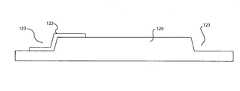
- FIG. 2is a schematic block diagram of the wafer 240 positioned on the chuck 250 in a test environment according to an embodiment of the present invention. Spaced apart from the wafer 240 and facing in opposition thereto is the probe card 110 .
- the probe card 110includes a base 112 , a gasket 115 , an anti-wafer 120 , and an isolation layer 130 .
- the base 112may comprise a ceramic plate or a printed circuit board (PCB), for example. Electrical connections from the tester 101 (see FIG. 1 ) may be terminated on the base 112 .
- the cable 103may have a connector that connects to a matching terminal on the base 112 .
- Electrical connections between the base 112 and the anti-wafer 120may be made by way of wirings 129 .
- the wirings 129electrically contact the anti-wafer 120 using solder balls formed on electrically conductive cantilevers 122 .
- a number of electrically conducting cantilevers 122may be formed on the anti-wafer 120 .
- a number of electrically conducting probes 128extend from unsupported ends of the cantilevers 122 .
- the cantilevers 122may include, for example, a single homogenous layer of a material that is both flexible and conductive, or a bi-layer structure including a metal layer, such as aluminum (Al), deposited over a mechanical layer of a tractable or flexible dielectric material, such as an oxide or a nitride.
- the probes 128may include a pin (i.e., main body) comprising a first metal and having a first cross-sectional area, and a tip 131 comprising a second metal and having a second cross-sectional area smaller than the first cross-sectional area.
- the pin of a probe 128comprises copper, nickel, or alloys thereof, while its tip 131 comprises nickel, gold or alloys thereof.
- Both the cantilevers 122 and the probes 128may be formed using standard deposition, photolithographic, and etching techniques widely known and used in semiconductor processing and microelectromechanical systems (MEMs) fabrication.
- the anti-wafer 120may be divided into a plurality of probe dice, with each probe die having one or more probes 128 , cantilevers 122 , and cavities 124 . Each probe die may be used to test a corresponding die on the wafer 240 .
- each of the cantilevers 122projects over one of a number of cavities 124 formed on the surface of the anti-wafer 120 .
- the cavities 124advantageously enable the unsupported ends of the cantilevers 122 to flex or deform downward under force applied to the probe card 110 and/or the wafer 240 (“wafer under test”), thereby compensating for much greater variations in planarity of the probe card or the wafer 240 , and/or differences in parallelism between the probe card 110 and the wafer 240 , than possible in conventional cantilever probe cards.
- a single cavity 124may have a depth sufficient to enable free movement of a cantilever 122 , or may have a cross-sectional surface area tailored to accommodate more than one cantilever 122 .
- the cavities 124may extend substantially entirely through the anti-wafer 120 , and may be formed through the backside of the anti-wafer 120 .
- the cavities 124may be filled with a compressive material, such as polyimide.
- a compressive layersuch as an electrically insulating interposer 130
- the interposer 130may be formed on or disposed above the surface of the anti-wafer 120 with a number of holes through which the probes 128 extend.
- the interposer 130comprises an elastomer capable of flexing or compressing under force or pressure, thereby further compensating for variations in planarity or parallelism.
- the interposer 130comprises a layer of polyimide, having a thickness equal to or less than about 300 microns ( ⁇ m).
- a relatively thin capping layer 132may be formed on the surface of the interposer 130 facing the wafer 240 to protect the interposer during formation of holes therein.
- the capping layer 132may comprise silicon nitride, for example.
- the anti-wafer 120is so named because it may comprise a semiconductor substrate or a wafer having a silicon on insulator (SOI) layer with a number of contact points (e.g., probes 128 or pads) formed thereon, the layout of the contact points corresponding to a layout of pads 241 on the wafer 240 under test.
- the pads 241which may be on dice on the wafer 240 , are electrically connected to circuits of devices being tested.
- a probe 128contacts a corresponding pad 241 , thereby forming an electrical connection between the wafer 240 and the probe card 110 .
- the probe card 110includes a number of electrically conducting wirings 129 for electrically coupling the probes 128 through cantilevers 122 to a number of test circuits in the tester 101 .
- the anti-wafer 120may comprise a semiconductor substrate, one or more test circuits may be formed in the anti-wafer 120 , thereby off-loading some or all of the testing functions from the tester 101 , enabling more rapid testing and the use of less complex and therefore less expensive testers.
- the test circuit formed in the anti-wafer 120may be designed or optimized to test that specific integrated circuit or device under test.
- the anti-wafer 120may further include a gasket 115 .
- the gasket 115may abut a backside surface of the anti-wafer and the base 112 to further increase co-planarity between the surface of the anti-wafer 120 and the surface of the wafer 240 being tested.
- FIG. 3there is shown a schematic planar view of an anti-wafer 120 having a plurality of probe dice 121 according to an embodiment of the present invention. Note that only some of the probe dice 121 are labeled in the interest of clarity.
- a probe die 121may have a probe layout that matches contact points on a corresponding die on the wafer 240 . As can be appreciated, the probe layout of a probe die 121 may be personalized for a particular die on the wafer 240 being tested.
- Each probe die 121may have at least one cantilever 122 projecting over a cavity 124 formed on the surface thereof, and a probe 128 extending from the unsupported end of the cantilever 122 (see FIG. 2 ).
- the probe diceare separated from one another by a number of intersecting grooves or recesses 123 .
- the recesses 123can be arranged on the surface of the anti-wafer 120 to create a crisscross pattern.
- the recesses 123can be formed on the anti-wafer 120 using semiconductor processing or MEMs fabrication techniques. A process for forming these recesses is further described below.
- FIGS. 4 and 5show further details of the probe dice 121 and the recesses 123 .
- FIG. 4is schematic planar view of a portion of the anti-wafer 120 of FIG. 3 showing four of the probe dice 121 with crisscrossed recesses 123 therebetween.
- FIG. 5is schematic cross-sectional view taken along sections A-A of FIG. 4 .
- FIG. 5shows a portion of two adjacent probe dice 121 and a recess 123 formed between them according to an embodiment of the present invention.
- a recess 123advantageously accommodates a wiring 129 or other electrical interconnection to a probe die 121 to prevent scratching the surface of a wafer being tested.
- the methodinvolves: (i) forming a pattern of intersecting recesses or grooves on the surface of a substrate; (ii) depositing a conformal conductive layer over the patterned surface of the substrate; (iii) patterning the conductive layer to form one or more beams, which will be further processed to form one or more cantilever structures on raised portions on the surface of the substrate and a number of contacts or pads on which the contacts will subsequently be formed in the recesses; (iii) depositing an electrically insulating material on the raised portions on the surface of the substrate to form a number of electrically insulating compressive layers; (iv) forming a number of openings extending through the electrically insulating material from a top surface thereof, each of the openings intersecting with and exposing a portion of one of the beams formed in the patterned conducting
- a pattern of crisscrossed recesses 123is formed on the surface of an anti-wafer 120 .
- the anti-wafer 120comprises a silicon substrate.
- the step of forming a pattern of intersecting recesses or grooves on the surface of the substrateincludes the step of forming a grid of recesses 123 , as shown in FIGS. 3-5 , on a single crystal silicon substrate using a KOH etch process.
- a conformal conductive layeris deposited on the sample of FIG. 6 ( a ), and then patterned to form one or more structures that will be become cantilevers 122 .
- the step of depositing a conformal conductive layercan involve depositing a single layer of metal, such as Aluminum, or a bi-layer of an upper conductive material and second non-conductive layer having the desired mechanical properties, i.e., strength and flexibility.
- the conformal conductive layercan include an Al layer over a Silicon Oxide (SiO2) layer.
- the step of patterning the conductive layer to form one or more structures (and contacts or pads in the recesses),can be accomplished using standard and known photolithographic processes.
- this stepinvolves electro-deposition (ED) of photoresist to provide a substantially uniform PR mask over the surface with the recesses or grooves formed therein.
- EDelectro-deposition
- Etching of the conductive layercan then be performed using any standard technique having a suitable selectivity to the substrate.
- an electrically insulating materialis deposited on raised (i.e., not on recesses 123 ) portions of the anti-wafer 120 to form a number of electrically insulating compressive layers, such as interposers 601 .
- the step of depositing an electrically insulating compressive layer on the raised portions on the surface of the anti-wafer 120comprises depositing a flexible or tractable resilient material such as polyimide.
- One or more openings 631are then formed through the interposers 601 . Each opening 631 extends from the top of the interposer 601 and intersect with and exposes what would become an unsupported end of a cantilever 122 .
- the openings 631are then filled with an electrically conductive material to form one or more probes 128 extending from the exposed beam portions of the cantilevers 122 .
- the step of filling each of the openings 631includes filing the openings 631 with a copper (Cu) and nickel (Ni) alloy to form the probes 128 .
- etch release holes 632are formed through the interposers 601 .
- Each release hole 632extends from the top of the interposer 601 and ends on a surface of the anti-wafer 120 where a cavity 124 (see FIG. 6 ( e )) will be formed under the unsupported end of a cantilever 122 .
- the etch release hole 632 shown in FIG. 6 ( d )is not to scale and is generally a lot smaller than that for the probe 128 . It is to be further noted that only one etch release hole 632 is shown in FIG. 6 ( d ) for clarity of illustration.
- the step of forming a number of etch release holes 632generally includes forming a sufficient number of holes having a sufficient cross-sectional area to completely release the unsupported end of the cantilevers, without unduly weakening the substrate or causing one cavity to open to another.
- one or more cavities 124are formed on the surface of the anti-wafer 120 .
- Each cavity 124allows an unsupported portion of a cantilever 122 to flex when a probe 128 is pushed in a direction towards the cavity 124 .
- the cavities 124may be formed by etching or removing a portion of the surface of the anti-wafer 120 adjacent to the ends of the cantilevers 122 .
- the unsupported portions of cantilevers 122are released by etching or removing the desired portions of the anti-wafer 120 using a xenon difluoride (XeF2) etch process.
- XeF2xenon difluoride
- the XeF 2is sublimated in a separate container or vessel to a pressure of about 4 mTorr (the vapor pressure of XeF 2 ), and then introduced into the first chamber.
- the XeF 2 release or etching processis performed in vapor phase at a pressure of 60 mTorr, at room temperature and with no external energy sources. Under these conditions, a highly selective and isotropic etch of silicon has been observed with rates as high as 10 microns per minute.
- the XeF 2 release processis allowed to proceed without etching any of the cantilever or interposer material until substantially all of the unsupported ends of the cantilevers 122 are released and the cavities 124 having the desired dimensions are formed.
- a wiring 129may be electrically coupled to a cantilever 122 .
- the wiring 129is electrically coupled to the cantilever 122 using a solder ball 601 .
- Placement of the solder ball 601 and the wiring 129 in the recesses 123 below the raised surface of the anti-wafer 120advantageously minimizes or avoids entirely possible damage to the wafer under test due to scrubbing of the wafer under test with a connector, and enables use of a thinner interposer 601 .
- the sample of FIG. 6 ( e )may be further processed by capping the interposers 601 with a silicon nitride layer, and/or forming Ni/Gold (Au) tips on the probes 128 .
- the advantages of the probe card of the present invention over previous or conventional techniquesinclude: (i) reduction in costs of probe cards; (ii) reduction in manufacturing time for new probe cards having new configurations to test new product wafers; and (iii) ability to offload a number of functions to on board test circuitry in the anti-wafer of the probe card, thereby enabling low cost testers to be utilized.
Landscapes
- Physics & Mathematics (AREA)
- General Physics & Mathematics (AREA)
- Testing Or Measuring Of Semiconductors Or The Like (AREA)
- Measuring Leads Or Probes (AREA)
Abstract
Description
- This application is a divisional of U.S. application Ser. No. 11/084,671, filed on Mar. 18, 2005, which claims the benefit of U.S. Provisional Application No. 60/556,556, filed on Mar. 26, 2004. Both of the aforementioned disclosures are incorporated herein by reference in their entirety.
- 1. Field of the Invention
- The present invention relates generally to methods and apparatus for testing integrated circuits, and more particularly to advanced probe cards and methods of fabricating the same.
- 2. Description of the Background Art
- Probe cards are used in the testing of integrated circuits (ICs) by providing an interface between the pads of a bare die or chip formed on a wafer or substrate and test equipment.
- One conventional type of probe card uses a large number of cantilevered arms extending obliquely outwardly from the planar surface of a substrate or a printed circuit board (PCB). Probe pins having needle-like tips extend from distal ends of the cantilevered arms to provide electrical contact with the pads on the die. The probe pins or the tips are typically made of a hard material, such as tungsten, to extend the operating life of the probe card. When the wafer is raised beyond the point at which the first pads on the die first come into contact with these tips, the arms flex so as to allow remaining tips on other arms to contact pads on the die, thereby compensating for any small variations in planarity or parallelism between the probe card and die or chip on the surface of the wafer. In addition, movement of the wafer past the point at which the tips contact pads on the die and the resultant flexing of the cantilever arms cause the tips to scrub across their respective pads thereby removing oxide buildup on the pads, and improving electrical contact between the probe card and the die.
- One disadvantage of the above conventional approach is that the hardness of the tips of the probe pins and the typically limited movement of the cantilever arms can compensate for only small variations in planarity or parallelism between the surface of the die and the probe card. Moreover, even under ideal circumstances, the wafer typically receives some damage from the probe tip touch down. Thus, if the probe card is pushed against the wafer with a greater than usual force, such as to compensate for non-planarity or lack of parallelism, there is substantial likelihood that the wafer will be destroyed.
- Another commonly used type of conventional probe card uses micro spring probes eliminating the need for cantilevered arms, and reducing if not eliminating damage to the wafer from solid tungsten probe pins. However, most spring probes have inherent limitations, such as limited pitch and limited pin count due to the size of the springs. More fundamentally, micro-spring probe cards have a substantially higher cost of fabrication than conventional cantilever probe cards.
- Other additional disadvantages of both types of conventional probe cards include high cost, since a new or reconfigured probe card must be produced for each new IC layout, and long lead times required to produce a new or reconfigured probe card resulting in delays in chip production. This last problem arises because the layout or configuration of the probe card generally cannot be determined until the final mask for the IC is produced. Thus, availability of a probe card to test an IC can lag the initial production of the IC by four weeks or more.
- Accordingly, there is a need for a probe card and a method using the same that are capable of compensating for significant variations in planarity or parallelism between the wafer and the probe card, without increasing the possibility of damage to the wafer. It is desirable that the probe card has a low cost relative to conventional advanced or high pin count probe cards. It is further desirable that new probe cards having a new configuration can be manufactured quickly, to reduce if not eliminate impact on chip production.
- In one aspect, the present invention is directed to a probe card for testing a number of dice under test (DUTs) on a wafer. Generally, the probe card includes a substrate, a number of electrically conducting cantilevers formed on a surface of the substrate, and a number of electrically conducting probes extending from unsupported ends of the cantilevers. The unsupported end of each of the cantilevers projects over one of a number of cavities formed in the surface of the substrate. Each of the probes having a tip adapted for contacting a pad on a surface of the DUT. Preferably, the probes include a pin made of a first material and having a first cross-sectional area, and the tip is made of a second material and having a second cross-sectional area smaller than the first cross-sectional area.
- In one embodiment, the probe card further includes an electrically insulating compressive layer, such as an interposer, disposed above the surface of the substrate, the compressive layer having a number of holes extending therethrough and through which the probes extend to contact the pads on the surface of the DUT. Preferably, the compressive layer has a thickness of equal to or less than 300 microns. More preferably, the compressive layer includes polyimide, and wherein the compressive layer further includes a thin nitride capping layer on a top surface thereof.
- In another embodiment, the substrate includes an anti-wafer having a number of electrically conducting interconnects formed therein for electrically coupling the probes through cantilevers to a number of test circuits. The substrate can further include a gasket abutting a backside surface of the anti-wafer and a plate of a test apparatus in which the probe card is held, to adjust for non-coplanarity between the surface of the substrate and the surface of the DUT. In one version of this embodiment, at least one of the test circuits is formed in the anti-wafer. In another version of this embodiment, the anti-wafer is divided into a number of probe dice, and each of the probe dice include at least one cantilever projecting over a cavity formed in the surface of the probe dice, and a probe extending from the unsupported end of the cantilever. The cavity may be left empty or filled with a compressive material, for example. Preferably, the probe dice are separated from one another by a number of intersecting recesses or grooves. More preferably, the cantilevers are electrically coupled to the test circuits through the interconnects in the anti-wafer and electrical contacts formed in the intersecting recesses.
- In another aspect, the invention is directed to a method of fabricating a probe card such as those described above.
- These and various other features and advantages of the present invention will be apparent upon reading of the following detailed description in conjunction with the accompanying drawings and the appended claims provided below, where:
FIG. 1 is a schematic block diagram of a test environment according to an embodiment of the present invention.FIG. 2 is a schematic block diagram of wafer positioned on a chuck in a test environment according to an embodiment of the present invention;FIG. 3 is schematic planar view of an anti-wafer having a plurality of probe dice according to an embodiment of the present invention;FIG. 4 is schematic planar view of a portion of the anti-wafer ofFIG. 3 showing probe dice with criss-cross recesses therebetween according to an embodiment of the present invention;FIG. 5 is schematic cross-sectional view of a portion of the probe dice ofFIG. 4 showing the recess formed between adjacent probe dice according to an embodiment of the present invention; and- FIGS.6(a)-6(e) schematically illustrate the fabrication of a probe card according to an embodiment of the present invention.
- The figures are not drawn to scale.
- The present invention is directed to a probe card, and to methods of manufacturing and using the same for testing integrated circuits (ICs) formed in dice of a wafer or semiconductor substrate.
- A probe card according to an embodiment of the present invention will now be described in greater detail with reference to FIGS.1 to6. For purposes of clarity, many of the details of testing semiconductor devices or ICs in general, and probe cards in particular, that are widely known and are not relevant to the present invention have been omitted from the following description. Probe cards and IC testing are described in, for example, commonly assigned U.S. Pat. Nos. 6,847,218 and 6,759,865, which are incorporated herein by reference in their entirety.
FIG. 1 is a schematic block diagram of atest environment 160 in accordance with an embodiment of the present invention. In the example ofFIG. 1 , thetest environment 160 includes atester 101 and aprober 100. Thetester 101 may be a commercially available test equipment product such as those of the type available from Advantest Corporation, for example. Thetester 101 is electrically coupled to theprober 100 using acable 103. Theprober 100 may include aprobe card 110, which in turn may include ananti wafer 120. As will be more apparent below, the anti-wafer120 provides a removable electrical connection to awafer 240. Thewafer 240 includes a plurality dice, each die having one or more devices under test (DUTs). Thewafer 240 may be supported by aprobe chuck 250, which may be of the type similar to those available from the Electroglas company. During a test run, the anti-wafer120, thewafer 240, or both are positioned such that one or more probes on the anti-wafer120 touch contact points on thewafer 240. This allows thetester 101 to send stimulus signals to thewafer 240 via a path that includes thecable 103, theprobe card 110, and the anti-wafer120. Similarly, thetester 101 may receive response signals from thewafer 240 over the same path.FIG. 2 is a schematic block diagram of thewafer 240 positioned on thechuck 250 in a test environment according to an embodiment of the present invention. Spaced apart from thewafer 240 and facing in opposition thereto is theprobe card 110. In the example ofFIG. 2 , theprobe card 110 includes abase 112, agasket 115, an anti-wafer120, and anisolation layer 130.- The base112 may comprise a ceramic plate or a printed circuit board (PCB), for example. Electrical connections from the tester101 (see
FIG. 1 ) may be terminated on thebase 112. For example, thecable 103 may have a connector that connects to a matching terminal on thebase 112. Electrical connections between the base112 and the anti-wafer120 may be made by way ofwirings 129. In the example ofFIG. 2 , thewirings 129 electrically contact the anti-wafer120 using solder balls formed on electricallyconductive cantilevers 122. - A number of electrically conducting
cantilevers 122 may be formed on the anti-wafer120. In the example ofFIG. 2 , a number of electrically conductingprobes 128 extend from unsupported ends of thecantilevers 122. Thecantilevers 122 may include, for example, a single homogenous layer of a material that is both flexible and conductive, or a bi-layer structure including a metal layer, such as aluminum (Al), deposited over a mechanical layer of a tractable or flexible dielectric material, such as an oxide or a nitride. Theprobes 128 may include a pin (i.e., main body) comprising a first metal and having a first cross-sectional area, and atip 131 comprising a second metal and having a second cross-sectional area smaller than the first cross-sectional area. Preferably, the pin of aprobe 128 comprises copper, nickel, or alloys thereof, while itstip 131 comprises nickel, gold or alloys thereof. Both thecantilevers 122 and theprobes 128 may be formed using standard deposition, photolithographic, and etching techniques widely known and used in semiconductor processing and microelectromechanical systems (MEMs) fabrication. As will be further discussed below, the anti-wafer120 may be divided into a plurality of probe dice, with each probe die having one ormore probes 128,cantilevers 122, andcavities 124. Each probe die may be used to test a corresponding die on thewafer 240. - The unsupported end of each of the
cantilevers 122 projects over one of a number ofcavities 124 formed on the surface of the anti-wafer120. Thecavities 124 advantageously enable the unsupported ends of thecantilevers 122 to flex or deform downward under force applied to theprobe card 110 and/or the wafer240 (“wafer under test”), thereby compensating for much greater variations in planarity of the probe card or thewafer 240, and/or differences in parallelism between theprobe card 110 and thewafer 240, than possible in conventional cantilever probe cards. Asingle cavity 124 may have a depth sufficient to enable free movement of acantilever 122, or may have a cross-sectional surface area tailored to accommodate more than onecantilever 122. Optionally, thecavities 124 may extend substantially entirely through the anti-wafer120, and may be formed through the backside of the anti-wafer120. Optionally, thecavities 124 may be filled with a compressive material, such as polyimide. - A compressive layer, such as an electrically insulating
interposer 130, may be formed on or disposed above the surface of the anti-wafer120 with a number of holes through which theprobes 128 extend. Preferably, theinterposer 130 comprises an elastomer capable of flexing or compressing under force or pressure, thereby further compensating for variations in planarity or parallelism. In one embodiment, theinterposer 130 comprises a layer of polyimide, having a thickness equal to or less than about 300 microns (μm). A relatively thin capping layer132 may be formed on the surface of theinterposer 130 facing thewafer 240 to protect the interposer during formation of holes therein. The capping layer132 may comprise silicon nitride, for example. - The anti-wafer120 is so named because it may comprise a semiconductor substrate or a wafer having a silicon on insulator (SOI) layer with a number of contact points (e.g., probes128 or pads) formed thereon, the layout of the contact points corresponding to a layout of
pads 241 on thewafer 240 under test. Thepads 241, which may be on dice on thewafer 240, are electrically connected to circuits of devices being tested. During testing, aprobe 128 contacts acorresponding pad 241, thereby forming an electrical connection between thewafer 240 and theprobe card 110. Theprobe card 110 includes a number of electrically conductingwirings 129 for electrically coupling theprobes 128 throughcantilevers 122 to a number of test circuits in thetester 101. - Because the anti-wafer120 may comprise a semiconductor substrate, one or more test circuits may be formed in the anti-wafer120, thereby off-loading some or all of the testing functions from the
tester 101, enabling more rapid testing and the use of less complex and therefore less expensive testers. Preferably, where the anti-wafer120 has a configuration, architecture or topology designed for use with a specific integrated circuit or device under test, the test circuit formed in the anti-wafer120 may be designed or optimized to test that specific integrated circuit or device under test. - As shown in
FIG. 2 , the anti-wafer120 may further include agasket 115. Thegasket 115 may abut a backside surface of the anti-wafer and the base112 to further increase co-planarity between the surface of the anti-wafer120 and the surface of thewafer 240 being tested. - Referring now to
FIG. 3 , there is shown a schematic planar view of an anti-wafer120 having a plurality ofprobe dice 121 according to an embodiment of the present invention. Note that only some of theprobe dice 121 are labeled in the interest of clarity. A probe die121 may have a probe layout that matches contact points on a corresponding die on thewafer 240. As can be appreciated, the probe layout of a probe die121 may be personalized for a particular die on thewafer 240 being tested. Each probe die121 may have at least onecantilever 122 projecting over acavity 124 formed on the surface thereof, and aprobe 128 extending from the unsupported end of the cantilever122 (seeFIG. 2 ). Preferably, the probe dice are separated from one another by a number of intersecting grooves or recesses123. As shown inFIG. 3 , therecesses 123 can be arranged on the surface of the anti-wafer120 to create a crisscross pattern. Therecesses 123 can be formed on the anti-wafer120 using semiconductor processing or MEMs fabrication techniques. A process for forming these recesses is further described below. FIGS. 4 and 5 show further details of theprobe dice 121 and therecesses 123. In particular,FIG. 4 is schematic planar view of a portion of the anti-wafer120 ofFIG. 3 showing four of theprobe dice 121 with crisscrossedrecesses 123 therebetween.FIG. 5 is schematic cross-sectional view taken along sections A-A ofFIG. 4 .FIG. 5 shows a portion of twoadjacent probe dice 121 and arecess 123 formed between them according to an embodiment of the present invention. As will be more apparent below, arecess 123 advantageously accommodates awiring 129 or other electrical interconnection to a probe die121 to prevent scratching the surface of a wafer being tested.- A method of fabricating a probe card in accordance with an embodiment of the present invention will now be described with reference to FIGS.6(a)-6(e). Generally, the method involves: (i) forming a pattern of intersecting recesses or grooves on the surface of a substrate; (ii) depositing a conformal conductive layer over the patterned surface of the substrate; (iii) patterning the conductive layer to form one or more beams, which will be further processed to form one or more cantilever structures on raised portions on the surface of the substrate and a number of contacts or pads on which the contacts will subsequently be formed in the recesses; (iii) depositing an electrically insulating material on the raised portions on the surface of the substrate to form a number of electrically insulating compressive layers; (iv) forming a number of openings extending through the electrically insulating material from a top surface thereof, each of the openings intersecting with and exposing a portion of one of the beams formed in the patterned conducting layer; (v) filling each of the openings with an electrically conductive material to form a number of electrically conducting probes extending from the exposed portions of the beams; (vi) forming a number of etch release holes extending from a top surface of each electrically insulating compressive layers and terminating on and exposing a portion of the substrate surface adjacent to one of the beams formed thereon; and (vii) etching or removing a portion of the substrate surface adjacent to the beams to release the beams, thereby forming a number of cantilevers, each having an unsupported end projecting over a cavity formed in the surface of the substrate.
- In
FIG. 6 (a), a pattern of crisscrossedrecesses 123 is formed on the surface of an anti-wafer120. In the example ofFIG. 6 (a), the anti-wafer120 comprises a silicon substrate. In one embodiment, the step of forming a pattern of intersecting recesses or grooves on the surface of the substrate includes the step of forming a grid ofrecesses 123, as shown inFIGS. 3-5 , on a single crystal silicon substrate using a KOH etch process. - In
FIG. 6 (b), a conformal conductive layer is deposited on the sample ofFIG. 6 (a), and then patterned to form one or more structures that will be become cantilevers122. The step of depositing a conformal conductive layer can involve depositing a single layer of metal, such as Aluminum, or a bi-layer of an upper conductive material and second non-conductive layer having the desired mechanical properties, i.e., strength and flexibility. For example, the conformal conductive layer can include an Al layer over a Silicon Oxide (SiO2) layer. The step of patterning the conductive layer to form one or more structures (and contacts or pads in the recesses), can be accomplished using standard and known photolithographic processes. In one embodiment, this step involves electro-deposition (ED) of photoresist to provide a substantially uniform PR mask over the surface with the recesses or grooves formed therein. Etching of the conductive layer can then be performed using any standard technique having a suitable selectivity to the substrate. - In
FIG. 6 (c), an electrically insulating material is deposited on raised (i.e., not on recesses123) portions of the anti-wafer120 to form a number of electrically insulating compressive layers, such asinterposers 601. In one embodiment, the step of depositing an electrically insulating compressive layer on the raised portions on the surface of the anti-wafer120 comprises depositing a flexible or tractable resilient material such as polyimide. One ormore openings 631 are then formed through theinterposers 601. Eachopening 631 extends from the top of theinterposer 601 and intersect with and exposes what would become an unsupported end of acantilever 122. Theopenings 631 are then filled with an electrically conductive material to form one ormore probes 128 extending from the exposed beam portions of thecantilevers 122. Preferably, the step of filling each of theopenings 631 includes filing theopenings 631 with a copper (Cu) and nickel (Ni) alloy to form theprobes 128. - In
FIG. 6 (d), a number of etch release holes632 are formed through theinterposers 601. Eachrelease hole 632 extends from the top of theinterposer 601 and ends on a surface of the anti-wafer120 where a cavity124 (seeFIG. 6 (e)) will be formed under the unsupported end of acantilever 122. Note that theetch release hole 632 shown inFIG. 6 (d) is not to scale and is generally a lot smaller than that for theprobe 128. It is to be further noted that only oneetch release hole 632 is shown inFIG. 6 (d) for clarity of illustration. The step of forming a number of etch release holes632 generally includes forming a sufficient number of holes having a sufficient cross-sectional area to completely release the unsupported end of the cantilevers, without unduly weakening the substrate or causing one cavity to open to another. - In
FIG. 6 (e), one ormore cavities 124 are formed on the surface of the anti-wafer120. Eachcavity 124 allows an unsupported portion of acantilever 122 to flex when aprobe 128 is pushed in a direction towards thecavity 124. Thecavities 124 may be formed by etching or removing a portion of the surface of the anti-wafer120 adjacent to the ends of thecantilevers 122. In one embodiment, the unsupported portions ofcantilevers 122 are released by etching or removing the desired portions of the anti-wafer120 using a xenon difluoride (XeF2) etch process. According to one embodiment of the invention, the sample ofFIG. 6 (d) is placed in a first chamber or vessel that is purged, typically with nitrogen, and evacuated down to a moderate vacuum. The XeF2is sublimated in a separate container or vessel to a pressure of about 4 mTorr (the vapor pressure of XeF2), and then introduced into the first chamber. Preferably, the XeF2release or etching process is performed in vapor phase at a pressure of 60 mTorr, at room temperature and with no external energy sources. Under these conditions, a highly selective and isotropic etch of silicon has been observed with rates as high as 10 microns per minute. The XeF2release process is allowed to proceed without etching any of the cantilever or interposer material until substantially all of the unsupported ends of thecantilevers 122 are released and thecavities 124 having the desired dimensions are formed. - Still referring to
FIG. 6 (e), awiring 129 may be electrically coupled to acantilever 122. In the example ofFIG. 6 (e), thewiring 129 is electrically coupled to thecantilever 122 using asolder ball 601. Placement of thesolder ball 601 and thewiring 129 in therecesses 123 below the raised surface of the anti-wafer120 advantageously minimizes or avoids entirely possible damage to the wafer under test due to scrubbing of the wafer under test with a connector, and enables use of athinner interposer 601. - The sample of
FIG. 6 (e) may be further processed by capping theinterposers 601 with a silicon nitride layer, and/or forming Ni/Gold (Au) tips on theprobes 128. - The advantages of the probe card of the present invention over previous or conventional techniques include: (i) reduction in costs of probe cards; (ii) reduction in manufacturing time for new probe cards having new configurations to test new product wafers; and (iii) ability to offload a number of functions to on board test circuitry in the anti-wafer of the probe card, thereby enabling low cost testers to be utilized.
- The foregoing description of specific embodiments and examples of the invention have been presented for the purpose of illustration and description, and although the invention has been described and illustrated by certain of the preceding examples, it is not to be construed as being limited thereby. They are not intended to be exhaustive or to limit the invention to the precise forms disclosed, and many modifications, improvements and variations within the scope of the invention are possible in light of the above teaching. It is intended that the scope of the invention encompass the generic area as herein disclosed, and by the claims appended hereto and their equivalents.
Claims (16)
Priority Applications (1)
| Application Number | Priority Date | Filing Date | Title |
|---|---|---|---|
| US12/008,483US7685705B2 (en) | 2004-03-26 | 2008-01-11 | Method of fabricating a probe card |
Applications Claiming Priority (3)
| Application Number | Priority Date | Filing Date | Title |
|---|---|---|---|
| US55655604P | 2004-03-26 | 2004-03-26 | |
| US11/084,671US7332921B2 (en) | 2004-03-26 | 2005-03-18 | Probe card and method for constructing same |
| US12/008,483US7685705B2 (en) | 2004-03-26 | 2008-01-11 | Method of fabricating a probe card |
Related Parent Applications (1)
| Application Number | Title | Priority Date | Filing Date |
|---|---|---|---|
| US11/084,671DivisionUS7332921B2 (en) | 2004-03-26 | 2005-03-18 | Probe card and method for constructing same |
Publications (2)
| Publication Number | Publication Date |
|---|---|
| US20080110019A1true US20080110019A1 (en) | 2008-05-15 |
| US7685705B2 US7685705B2 (en) | 2010-03-30 |
Family
ID=34989054
Family Applications (2)
| Application Number | Title | Priority Date | Filing Date |
|---|---|---|---|
| US11/084,671Expired - Fee RelatedUS7332921B2 (en) | 2004-03-26 | 2005-03-18 | Probe card and method for constructing same |
| US12/008,483Expired - Fee RelatedUS7685705B2 (en) | 2004-03-26 | 2008-01-11 | Method of fabricating a probe card |
Family Applications Before (1)
| Application Number | Title | Priority Date | Filing Date |
|---|---|---|---|
| US11/084,671Expired - Fee RelatedUS7332921B2 (en) | 2004-03-26 | 2005-03-18 | Probe card and method for constructing same |
Country Status (3)
| Country | Link |
|---|---|
| US (2) | US7332921B2 (en) |
| TW (1) | TWI368740B (en) |
| WO (1) | WO2005098462A2 (en) |
Cited By (2)
| Publication number | Priority date | Publication date | Assignee | Title |
|---|---|---|---|---|
| US20120119208A1 (en)* | 2010-11-16 | 2012-05-17 | Hynix Semiconductor Inc. | Semiconductor apparatus and fabricating method thereof |
| WO2022204277A1 (en)* | 2021-03-23 | 2022-09-29 | Nielson Scientific Llc | Cryogenic probe card |
Families Citing this family (19)
| Publication number | Priority date | Publication date | Assignee | Title |
|---|---|---|---|---|
| US6812718B1 (en) | 1999-05-27 | 2004-11-02 | Nanonexus, Inc. | Massively parallel interface for electronic circuits |
| US7247035B2 (en) | 2000-06-20 | 2007-07-24 | Nanonexus, Inc. | Enhanced stress metal spring contactor |
| US7349223B2 (en) | 2000-05-23 | 2008-03-25 | Nanonexus, Inc. | Enhanced compliant probe card systems having improved planarity |
| US7382142B2 (en) | 2000-05-23 | 2008-06-03 | Nanonexus, Inc. | High density interconnect system having rapid fabrication cycle |
| US7952373B2 (en)* | 2000-05-23 | 2011-05-31 | Verigy (Singapore) Pte. Ltd. | Construction structures and manufacturing processes for integrated circuit wafer probe card assemblies |
| US7579848B2 (en) | 2000-05-23 | 2009-08-25 | Nanonexus, Inc. | High density interconnect system for IC packages and interconnect assemblies |
| US7332921B2 (en)* | 2004-03-26 | 2008-02-19 | Cypress Semiconductor Corporation | Probe card and method for constructing same |
| JP4535494B2 (en)* | 2004-10-20 | 2010-09-01 | ルネサスエレクトロニクス株式会社 | Thin film probe sheet manufacturing method and semiconductor chip inspection method |
| US7489151B2 (en)* | 2005-10-03 | 2009-02-10 | Pdf Solutions, Inc. | Layout for DUT arrays used in semiconductor wafer testing |
| TWI276805B (en)* | 2005-11-10 | 2007-03-21 | Mjc Probe Inc | Probe of probe card and manufacturing method thereof |
| US7723980B2 (en)* | 2007-03-22 | 2010-05-25 | Advanced Inquiry Systems, Inc. | Fully tested wafers having bond pads undamaged by probing and applications thereof |
| JP6305736B2 (en) | 2013-11-20 | 2018-04-04 | 測位衛星技術株式会社 | Information management system, data bank apparatus, data management method, database management method, and program |
| US9459288B2 (en)* | 2014-01-16 | 2016-10-04 | Infineon Technologies Ag | Wide interposer for an electronic testing system |
| WO2016122476A1 (en)* | 2015-01-28 | 2016-08-04 | Hewlett-Packard Development Company, L.P. | Interposer device |
| US11215641B2 (en)* | 2019-12-24 | 2022-01-04 | Teradyne, Inc. | Probe card assembly in automated test equipment |
| US11162980B2 (en) | 2019-12-24 | 2021-11-02 | Teradyne, Inc. | Coaxial via arrangement in probe card for automated test equipment |
| US11333683B2 (en) | 2019-12-24 | 2022-05-17 | Teradyne, Inc. | Transposed via arrangement in probe card for automated test equipment |
| US11340260B2 (en) | 2019-12-24 | 2022-05-24 | Teradyne, Inc. | Probe card pad geometry in automated test equipment |
| CN114545033B (en)* | 2020-11-03 | 2025-08-12 | 台湾中华精测科技股份有限公司 | Board connector, single arm type serial connection piece and wafer test assembly |
Citations (55)
| Publication number | Priority date | Publication date | Assignee | Title |
|---|---|---|---|---|
| US4232928A (en)* | 1979-06-27 | 1980-11-11 | Dit-Mco International Corporation | Apparatus employing flexible diaphragm for effecting substantially uniform force, individual couplings with multiple electrical contacts or the like |
| US4754316A (en)* | 1982-06-03 | 1988-06-28 | Texas Instruments Incorporated | Solid state interconnection system for three dimensional integrated circuit structures |
| US5061033A (en)* | 1990-12-03 | 1991-10-29 | Motorola, Inc. | Removable optical interconnect for electronic modules |
| US5070297A (en)* | 1990-06-04 | 1991-12-03 | Texas Instruments Incorporated | Full wafer integrated circuit testing device |
| US5172050A (en)* | 1991-02-15 | 1992-12-15 | Motorola, Inc. | Micromachined semiconductor probe card |
| US5338223A (en)* | 1991-09-03 | 1994-08-16 | At&T Bell Laboratories | Hybrid wafer probe |
| US5380318A (en)* | 1986-05-12 | 1995-01-10 | Surgical Laser Technologies, Inc. | Contact or insertion laser probe having wide angle radiation |
| US5477160A (en)* | 1992-08-12 | 1995-12-19 | Fujitsu Limited | Module test card |
| US5555422A (en)* | 1993-03-10 | 1996-09-10 | Co-Operative Facility For Aging Tester Development | Prober for semiconductor integrated circuit element wafer |
| US5600257A (en)* | 1995-08-09 | 1997-02-04 | International Business Machines Corporation | Semiconductor wafer test and burn-in |
| US5763879A (en)* | 1996-09-16 | 1998-06-09 | Pacific Western Systems | Diamond probe tip |
| US5807767A (en)* | 1996-01-02 | 1998-09-15 | Micron Technology, Inc. | Technique for attaching die to leads |
| US5811982A (en)* | 1995-11-27 | 1998-09-22 | International Business Machines Corporation | High density cantilevered probe for electronic devices |
| US5850148A (en)* | 1995-08-17 | 1998-12-15 | Nam; Jae W. | Vertical probe card apparatus with macro-tension module having notched-shaped needle for self-balancing contact |
| US5940965A (en)* | 1995-02-03 | 1999-08-24 | Hewlett-Packard Company | Method of making multiple lead voltage probe |
| US6060891A (en)* | 1997-02-11 | 2000-05-09 | Micron Technology, Inc. | Probe card for semiconductor wafers and method and system for testing wafers |
| US6064213A (en)* | 1993-11-16 | 2000-05-16 | Formfactor, Inc. | Wafer-level burn-in and test |
| US6075373A (en)* | 1996-05-31 | 2000-06-13 | Tokyo Electron Limited | Inspection device for inspecting a semiconductor wafer |
| US6074904A (en)* | 1998-04-21 | 2000-06-13 | Advanced Micro Devices, Inc. | Method and structure for isolating semiconductor devices after transistor formation |
| US6084215A (en)* | 1997-11-05 | 2000-07-04 | Tokyo Electron Limited | Semiconductor wafer holder with spring-mounted temperature measurement apparatus disposed therein |
| US6130104A (en)* | 1997-04-08 | 2000-10-10 | Tokyo Electron Limited | Cleaner for inspecting projections, and inspection apparatus and method for integrated circuits |
| US6146970A (en)* | 1998-05-26 | 2000-11-14 | Motorola Inc. | Capped shallow trench isolation and method of formation |
| US6208155B1 (en)* | 1998-01-27 | 2001-03-27 | Cerprobe Corporation | Probe tip and method for making electrical contact with a solder ball contact of an integrated circuit device |
| US6208947B1 (en)* | 1997-02-26 | 2001-03-27 | Micron Technology, Inc. | Method in an integrated circuit (IC) manufacturing process for identifying and redirecting IC's mis-processed during their manufacture |
| US6246245B1 (en)* | 1998-02-23 | 2001-06-12 | Micron Technology, Inc. | Probe card, test method and test system for semiconductor wafers |
| US6246250B1 (en)* | 1998-05-11 | 2001-06-12 | Micron Technology, Inc. | Probe card having on-board multiplex circuitry for expanding tester resources |
| US6400173B1 (en)* | 1999-11-19 | 2002-06-04 | Hitachi, Ltd. | Test system and manufacturing of semiconductor device |
| US6433563B1 (en)* | 1999-04-16 | 2002-08-13 | Fujitsu Limited | Probe card with rigid base having apertures for testing semiconductor device, and semiconductor device test method using probe card |
| US6452411B1 (en)* | 1999-03-01 | 2002-09-17 | Formfactor, Inc. | Efficient parallel testing of integrated circuit devices using a known good device to generate expected responses |
| US6469908B2 (en)* | 2000-03-31 | 2002-10-22 | Intel Corporation | Dual-socket interposer and method of fabrication therefor |
| US6469530B1 (en)* | 2000-02-15 | 2002-10-22 | Agilent Technologies, Inc. | Method and apparatus for testing of ball grid array circuitry |
| US6509213B2 (en)* | 1997-04-25 | 2003-01-21 | Micron Technology, Inc. | Methods of forming transistors and connections thereto |
| US6527563B2 (en)* | 2000-10-04 | 2003-03-04 | Gary A. Clayton | Grid interposer |
| US6531335B1 (en)* | 2000-04-28 | 2003-03-11 | Micron Technology, Inc. | Interposers including upwardly protruding dams, semiconductor device assemblies including the interposers, and methods |
| US6551844B1 (en)* | 1997-01-15 | 2003-04-22 | Formfactor, Inc. | Test assembly including a test die for testing a semiconductor product die |
| US6559666B2 (en)* | 1998-03-30 | 2003-05-06 | International Business Machines Corporation | Method and device for semiconductor testing using electrically conductive adhesives |
| US6563173B2 (en)* | 1998-01-20 | 2003-05-13 | International Business Machines Corporation | Silicon-on-insulator chip having an isolation barrier for reliability |
| US6627954B1 (en)* | 1999-03-19 | 2003-09-30 | Silicon Wave, Inc. | Integrated circuit capacitor in a silicon-on-insulator integrated circuit |
| US6627484B1 (en)* | 2000-11-13 | 2003-09-30 | Advanced Micro Devices, Inc. | Method of forming a buried interconnect on a semiconductor on insulator wafer and a device including a buried interconnect |
| US6661244B2 (en)* | 2000-03-06 | 2003-12-09 | Wentworth Laboratories, Inc. | Nickel alloy probe card frame laminate |
| US6664131B2 (en)* | 1999-07-13 | 2003-12-16 | Micron Technology, Inc. | Method of making ball grid array package with deflectable interconnect |
| US6724204B2 (en)* | 2001-04-18 | 2004-04-20 | Ic Mems, Inc. | Probe structure for testing semiconductor devices and method for fabricating the same |
| US6753238B2 (en)* | 2002-03-01 | 2004-06-22 | Nec Electronics Corporation | Semiconductor device and manufacturing method thereof |
| US6759858B2 (en)* | 1999-10-20 | 2004-07-06 | Intel Corporation | Integrated circuit test probe having ridge contact |
| US6759865B1 (en)* | 2002-07-30 | 2004-07-06 | Cypress Semiconductor Corporation | Array of dice for testing integrated circuits |
| US6774395B1 (en)* | 2003-01-15 | 2004-08-10 | Advanced Micro Devices, Inc. | Apparatus and methods for characterizing floating body effects in SOI devices |
| US6847218B1 (en)* | 2002-05-13 | 2005-01-25 | Cypress Semiconductor Corporation | Probe card with an adapter layer for testing integrated circuits |
| US6849928B2 (en)* | 2001-03-01 | 2005-02-01 | Chartered Semiconductor Manufacturing, Ltd | Dual silicon-on-insulator device wafer die |
| US6912778B2 (en)* | 2001-07-19 | 2005-07-05 | Micron Technology, Inc. | Methods of fabricating full-wafer silicon probe cards for burn-in and testing of semiconductor devices |
| US6922069B2 (en)* | 2003-04-11 | 2005-07-26 | Yulim Hitech, Inc. | Needle assembly of probe card |
| US7112975B1 (en)* | 2003-03-26 | 2006-09-26 | Cypress Semiconductor Corporation | Advanced probe card and method of fabricating same |
| US7112974B1 (en)* | 2002-05-23 | 2006-09-26 | Cypress Semiconductor Corporation | Proble for testing integrated circuits |
| US7145225B2 (en)* | 2002-03-04 | 2006-12-05 | Micron Technology, Inc. | Interposer configured to reduce the profiles of semiconductor device assemblies and packages including the same and methods |
| US7332921B2 (en)* | 2004-03-26 | 2008-02-19 | Cypress Semiconductor Corporation | Probe card and method for constructing same |
| US7381630B2 (en)* | 2001-01-02 | 2008-06-03 | The Charles Stark Draper Laboratory, Inc. | Method for integrating MEMS device and interposer |
Family Cites Families (3)
| Publication number | Priority date | Publication date | Assignee | Title |
|---|---|---|---|---|
| US5926029A (en)* | 1997-05-27 | 1999-07-20 | International Business Machines Corporation | Ultra fine probe contacts |
| US6483330B1 (en) | 2000-09-11 | 2002-11-19 | Eaglestone Partners I, Llc | Method for selecting components for a matched set using wafer interposers |
| JP2005233858A (en)* | 2004-02-23 | 2005-09-02 | Japan Electronic Materials Corp | Probe card |
- 2005
- 2005-03-18USUS11/084,671patent/US7332921B2/ennot_activeExpired - Fee Related
- 2005-03-24WOPCT/US2005/009984patent/WO2005098462A2/enactiveApplication Filing
- 2005-03-25TWTW094109340Apatent/TWI368740B/ennot_activeIP Right Cessation
- 2008
- 2008-01-11USUS12/008,483patent/US7685705B2/ennot_activeExpired - Fee Related
Patent Citations (56)
| Publication number | Priority date | Publication date | Assignee | Title |
|---|---|---|---|---|
| US4232928A (en)* | 1979-06-27 | 1980-11-11 | Dit-Mco International Corporation | Apparatus employing flexible diaphragm for effecting substantially uniform force, individual couplings with multiple electrical contacts or the like |
| US4754316A (en)* | 1982-06-03 | 1988-06-28 | Texas Instruments Incorporated | Solid state interconnection system for three dimensional integrated circuit structures |
| US5380318A (en)* | 1986-05-12 | 1995-01-10 | Surgical Laser Technologies, Inc. | Contact or insertion laser probe having wide angle radiation |
| US5070297A (en)* | 1990-06-04 | 1991-12-03 | Texas Instruments Incorporated | Full wafer integrated circuit testing device |
| US5061033A (en)* | 1990-12-03 | 1991-10-29 | Motorola, Inc. | Removable optical interconnect for electronic modules |
| US5172050A (en)* | 1991-02-15 | 1992-12-15 | Motorola, Inc. | Micromachined semiconductor probe card |
| US5338223A (en)* | 1991-09-03 | 1994-08-16 | At&T Bell Laboratories | Hybrid wafer probe |
| US5477160A (en)* | 1992-08-12 | 1995-12-19 | Fujitsu Limited | Module test card |
| US5555422A (en)* | 1993-03-10 | 1996-09-10 | Co-Operative Facility For Aging Tester Development | Prober for semiconductor integrated circuit element wafer |
| US6064213A (en)* | 1993-11-16 | 2000-05-16 | Formfactor, Inc. | Wafer-level burn-in and test |
| US5940965A (en)* | 1995-02-03 | 1999-08-24 | Hewlett-Packard Company | Method of making multiple lead voltage probe |
| US5600257A (en)* | 1995-08-09 | 1997-02-04 | International Business Machines Corporation | Semiconductor wafer test and burn-in |
| US5929651A (en)* | 1995-08-09 | 1999-07-27 | International Business Machines Corporation | Semiconductor wafer test and burn-in |
| US5850148A (en)* | 1995-08-17 | 1998-12-15 | Nam; Jae W. | Vertical probe card apparatus with macro-tension module having notched-shaped needle for self-balancing contact |
| US5811982A (en)* | 1995-11-27 | 1998-09-22 | International Business Machines Corporation | High density cantilevered probe for electronic devices |
| US5807767A (en)* | 1996-01-02 | 1998-09-15 | Micron Technology, Inc. | Technique for attaching die to leads |
| US6075373A (en)* | 1996-05-31 | 2000-06-13 | Tokyo Electron Limited | Inspection device for inspecting a semiconductor wafer |
| US5763879A (en)* | 1996-09-16 | 1998-06-09 | Pacific Western Systems | Diamond probe tip |
| US6551844B1 (en)* | 1997-01-15 | 2003-04-22 | Formfactor, Inc. | Test assembly including a test die for testing a semiconductor product die |
| US6060891A (en)* | 1997-02-11 | 2000-05-09 | Micron Technology, Inc. | Probe card for semiconductor wafers and method and system for testing wafers |
| US6208947B1 (en)* | 1997-02-26 | 2001-03-27 | Micron Technology, Inc. | Method in an integrated circuit (IC) manufacturing process for identifying and redirecting IC's mis-processed during their manufacture |
| US6130104A (en)* | 1997-04-08 | 2000-10-10 | Tokyo Electron Limited | Cleaner for inspecting projections, and inspection apparatus and method for integrated circuits |
| US6509213B2 (en)* | 1997-04-25 | 2003-01-21 | Micron Technology, Inc. | Methods of forming transistors and connections thereto |
| US6084215A (en)* | 1997-11-05 | 2000-07-04 | Tokyo Electron Limited | Semiconductor wafer holder with spring-mounted temperature measurement apparatus disposed therein |
| US6563173B2 (en)* | 1998-01-20 | 2003-05-13 | International Business Machines Corporation | Silicon-on-insulator chip having an isolation barrier for reliability |
| US6208155B1 (en)* | 1998-01-27 | 2001-03-27 | Cerprobe Corporation | Probe tip and method for making electrical contact with a solder ball contact of an integrated circuit device |
| US6246245B1 (en)* | 1998-02-23 | 2001-06-12 | Micron Technology, Inc. | Probe card, test method and test system for semiconductor wafers |
| US6559666B2 (en)* | 1998-03-30 | 2003-05-06 | International Business Machines Corporation | Method and device for semiconductor testing using electrically conductive adhesives |
| US6074904A (en)* | 1998-04-21 | 2000-06-13 | Advanced Micro Devices, Inc. | Method and structure for isolating semiconductor devices after transistor formation |
| US6246250B1 (en)* | 1998-05-11 | 2001-06-12 | Micron Technology, Inc. | Probe card having on-board multiplex circuitry for expanding tester resources |
| US6146970A (en)* | 1998-05-26 | 2000-11-14 | Motorola Inc. | Capped shallow trench isolation and method of formation |
| US6452411B1 (en)* | 1999-03-01 | 2002-09-17 | Formfactor, Inc. | Efficient parallel testing of integrated circuit devices using a known good device to generate expected responses |
| US6627954B1 (en)* | 1999-03-19 | 2003-09-30 | Silicon Wave, Inc. | Integrated circuit capacitor in a silicon-on-insulator integrated circuit |
| US6433563B1 (en)* | 1999-04-16 | 2002-08-13 | Fujitsu Limited | Probe card with rigid base having apertures for testing semiconductor device, and semiconductor device test method using probe card |
| US6664131B2 (en)* | 1999-07-13 | 2003-12-16 | Micron Technology, Inc. | Method of making ball grid array package with deflectable interconnect |
| US6759858B2 (en)* | 1999-10-20 | 2004-07-06 | Intel Corporation | Integrated circuit test probe having ridge contact |
| US6400173B1 (en)* | 1999-11-19 | 2002-06-04 | Hitachi, Ltd. | Test system and manufacturing of semiconductor device |
| US6469530B1 (en)* | 2000-02-15 | 2002-10-22 | Agilent Technologies, Inc. | Method and apparatus for testing of ball grid array circuitry |
| US6661244B2 (en)* | 2000-03-06 | 2003-12-09 | Wentworth Laboratories, Inc. | Nickel alloy probe card frame laminate |
| US6469908B2 (en)* | 2000-03-31 | 2002-10-22 | Intel Corporation | Dual-socket interposer and method of fabrication therefor |
| US6531335B1 (en)* | 2000-04-28 | 2003-03-11 | Micron Technology, Inc. | Interposers including upwardly protruding dams, semiconductor device assemblies including the interposers, and methods |
| US6527563B2 (en)* | 2000-10-04 | 2003-03-04 | Gary A. Clayton | Grid interposer |
| US6627484B1 (en)* | 2000-11-13 | 2003-09-30 | Advanced Micro Devices, Inc. | Method of forming a buried interconnect on a semiconductor on insulator wafer and a device including a buried interconnect |
| US7381630B2 (en)* | 2001-01-02 | 2008-06-03 | The Charles Stark Draper Laboratory, Inc. | Method for integrating MEMS device and interposer |
| US6849928B2 (en)* | 2001-03-01 | 2005-02-01 | Chartered Semiconductor Manufacturing, Ltd | Dual silicon-on-insulator device wafer die |
| US6724204B2 (en)* | 2001-04-18 | 2004-04-20 | Ic Mems, Inc. | Probe structure for testing semiconductor devices and method for fabricating the same |
| US6912778B2 (en)* | 2001-07-19 | 2005-07-05 | Micron Technology, Inc. | Methods of fabricating full-wafer silicon probe cards for burn-in and testing of semiconductor devices |
| US6753238B2 (en)* | 2002-03-01 | 2004-06-22 | Nec Electronics Corporation | Semiconductor device and manufacturing method thereof |
| US7145225B2 (en)* | 2002-03-04 | 2006-12-05 | Micron Technology, Inc. | Interposer configured to reduce the profiles of semiconductor device assemblies and packages including the same and methods |
| US6847218B1 (en)* | 2002-05-13 | 2005-01-25 | Cypress Semiconductor Corporation | Probe card with an adapter layer for testing integrated circuits |
| US7112974B1 (en)* | 2002-05-23 | 2006-09-26 | Cypress Semiconductor Corporation | Proble for testing integrated circuits |
| US6759865B1 (en)* | 2002-07-30 | 2004-07-06 | Cypress Semiconductor Corporation | Array of dice for testing integrated circuits |
| US6774395B1 (en)* | 2003-01-15 | 2004-08-10 | Advanced Micro Devices, Inc. | Apparatus and methods for characterizing floating body effects in SOI devices |
| US7112975B1 (en)* | 2003-03-26 | 2006-09-26 | Cypress Semiconductor Corporation | Advanced probe card and method of fabricating same |
| US6922069B2 (en)* | 2003-04-11 | 2005-07-26 | Yulim Hitech, Inc. | Needle assembly of probe card |
| US7332921B2 (en)* | 2004-03-26 | 2008-02-19 | Cypress Semiconductor Corporation | Probe card and method for constructing same |
Cited By (4)
| Publication number | Priority date | Publication date | Assignee | Title |
|---|---|---|---|---|
| US20120119208A1 (en)* | 2010-11-16 | 2012-05-17 | Hynix Semiconductor Inc. | Semiconductor apparatus and fabricating method thereof |
| WO2022204277A1 (en)* | 2021-03-23 | 2022-09-29 | Nielson Scientific Llc | Cryogenic probe card |
| JP2024516083A (en)* | 2021-03-23 | 2024-04-12 | ニールソン サイエンティフィック,エルエルシー | Cryogenic Probe Card |
| JP7743104B2 (en) | 2021-03-23 | 2025-09-24 | ニールソン サイエンティフィック,エルエルシー | Cryogenic Probe Card |
Also Published As
| Publication number | Publication date |
|---|---|
| TW200602641A (en) | 2006-01-16 |
| US7685705B2 (en) | 2010-03-30 |
| US7332921B2 (en) | 2008-02-19 |
| TWI368740B (en) | 2012-07-21 |
| WO2005098462A2 (en) | 2005-10-20 |
| US20050212540A1 (en) | 2005-09-29 |
| WO2005098462A3 (en) | 2006-08-17 |
Similar Documents
| Publication | Publication Date | Title |
|---|---|---|
| US7685705B2 (en) | Method of fabricating a probe card | |
| US8322020B2 (en) | Method for fabricating a semiconductor test probe card space transformer | |
| US7503811B2 (en) | Interconnection device for a printed circuit board, a method of manufacturing the same, and an interconnection assembly having the same | |
| KR101293348B1 (en) | Method to build a wirebond probe card in a many at a time fashion | |
| US6651325B2 (en) | Method for forming cantilever beam probe card and probe card formed | |
| US5625298A (en) | Semi-conductor chip test probe | |
| EP1292834B1 (en) | Systems for testing integrated circuits | |
| US7628620B2 (en) | Reinforced contact elements | |
| US7642793B2 (en) | Ultra-fine pitch probe card structure | |
| US20090079455A1 (en) | Reduced scrub contact element | |
| KR20010086060A (en) | Probe card for probing wafers with raised contact elements | |
| JP2003207523A (en) | Contactor, its manufacturing method and contact method | |
| JP2001091543A (en) | Semiconductor inspection equipment | |
| KR100523745B1 (en) | Microprobe and Method for Manufacturing the Same Using MEMS and Electroplating Technology | |
| KR100473584B1 (en) | Cantilever-type probe card and method for manufacturing the same using silicon micromachining technology | |
| US8917106B2 (en) | Fine pitch microelectronic contact array and method of making same | |
| US6660541B2 (en) | Semiconductor device and a manufacturing method thereof | |
| US8115504B2 (en) | Microspring array having reduced pitch contact elements | |
| TWI431278B (en) | Semiconductor test probe card space transformer | |
| JP2000171483A (en) | Manufacturing method of semiconductor inspection device | |
| KR101149808B1 (en) | Manufacturing method for probe and probe card | |
| KR100595373B1 (en) | Bridge type probe card and its manufacturing method | |
| WO2001084900A1 (en) | Connector apparatus | |
| JP2004207412A (en) | Inspection device and manufacturing method for semiconductor device |
Legal Events
| Date | Code | Title | Description |
|---|---|---|---|
| STCF | Information on status: patent grant | Free format text:PATENTED CASE | |
| FPAY | Fee payment | Year of fee payment:4 | |
| AS | Assignment | Owner name:MORGAN STANLEY SENIOR FUNDING, INC., NEW YORK Free format text:SECURITY INTEREST;ASSIGNORS:CYPRESS SEMICONDUCTOR CORPORATION;SPANSION LLC;REEL/FRAME:035240/0429 Effective date:20150312 | |
| MAFP | Maintenance fee payment | Free format text:PAYMENT OF MAINTENANCE FEE, 8TH YEAR, LARGE ENTITY (ORIGINAL EVENT CODE: M1552) Year of fee payment:8 | |
| AS | Assignment | Owner name:SPANSION LLC, CALIFORNIA Free format text:RELEASE BY SECURED PARTY;ASSIGNOR:MORGAN STANLEY SENIOR FUNDING, INC.;REEL/FRAME:047969/0552 Effective date:20181214 Owner name:CYPRESS SEMICONDUCTOR CORPORATION, CALIFORNIA Free format text:RELEASE BY SECURED PARTY;ASSIGNOR:MORGAN STANLEY SENIOR FUNDING, INC.;REEL/FRAME:047969/0552 Effective date:20181214 | |
| AS | Assignment | Owner name:MONTEREY RESEARCH, LLC, CALIFORNIA Free format text:ASSIGNMENT OF ASSIGNORS INTEREST;ASSIGNOR:CYPRESS SEMICONDUCTOR CORPORATION;REEL/FRAME:047947/0215 Effective date:20181214 | |
| AS | Assignment | Owner name:MORGAN STANLEY SENIOR FUNDING, INC., NEW YORK Free format text:CORRECTIVE ASSIGNMENT TO CORRECT THE 8647899 PREVIOUSLY RECORDED ON REEL 035240 FRAME 0429. ASSIGNOR(S) HEREBY CONFIRMS THE SECURITY INTERST;ASSIGNORS:CYPRESS SEMICONDUCTOR CORPORATION;SPANSION LLC;REEL/FRAME:058002/0470 Effective date:20150312 | |
| FEPP | Fee payment procedure | Free format text:MAINTENANCE FEE REMINDER MAILED (ORIGINAL EVENT CODE: REM.); ENTITY STATUS OF PATENT OWNER: LARGE ENTITY | |
| LAPS | Lapse for failure to pay maintenance fees | Free format text:PATENT EXPIRED FOR FAILURE TO PAY MAINTENANCE FEES (ORIGINAL EVENT CODE: EXP.); ENTITY STATUS OF PATENT OWNER: LARGE ENTITY | |
| STCH | Information on status: patent discontinuation | Free format text:PATENT EXPIRED DUE TO NONPAYMENT OF MAINTENANCE FEES UNDER 37 CFR 1.362 | |
| FP | Lapsed due to failure to pay maintenance fee | Effective date:20220330 |