US20080099795A1 - FinFET TRANSISTOR AND CIRCUIT - Google Patents
FinFET TRANSISTOR AND CIRCUITDownload PDFInfo
- Publication number
- US20080099795A1 US20080099795A1US11/969,339US96933908AUS2008099795A1US 20080099795 A1US20080099795 A1US 20080099795A1US 96933908 AUS96933908 AUS 96933908AUS 2008099795 A1US2008099795 A1US 2008099795A1
- Authority
- US
- United States
- Prior art keywords
- fin
- crystal
- doped
- plane
- source
- Prior art date
- Legal status (The legal status is an assumption and is not a legal conclusion. Google has not performed a legal analysis and makes no representation as to the accuracy of the status listed.)
- Granted
Links
Images


Classifications
- H—ELECTRICITY
- H10—SEMICONDUCTOR DEVICES; ELECTRIC SOLID-STATE DEVICES NOT OTHERWISE PROVIDED FOR
- H10D—INORGANIC ELECTRIC SEMICONDUCTOR DEVICES
- H10D30/00—Field-effect transistors [FET]
- H10D30/01—Manufacture or treatment
- H10D30/021—Manufacture or treatment of FETs having insulated gates [IGFET]
- H10D30/024—Manufacture or treatment of FETs having insulated gates [IGFET] of fin field-effect transistors [FinFET]
- H—ELECTRICITY
- H10—SEMICONDUCTOR DEVICES; ELECTRIC SOLID-STATE DEVICES NOT OTHERWISE PROVIDED FOR
- H10D—INORGANIC ELECTRIC SEMICONDUCTOR DEVICES
- H10D30/00—Field-effect transistors [FET]
- H10D30/60—Insulated-gate field-effect transistors [IGFET]
- H10D30/62—Fin field-effect transistors [FinFET]
- H—ELECTRICITY
- H10—SEMICONDUCTOR DEVICES; ELECTRIC SOLID-STATE DEVICES NOT OTHERWISE PROVIDED FOR
- H10D—INORGANIC ELECTRIC SEMICONDUCTOR DEVICES
- H10D62/00—Semiconductor bodies, or regions thereof, of devices having potential barriers
- H10D62/40—Crystalline structures
- H10D62/405—Orientations of crystalline planes
Definitions
- the present inventionrelates to the field of FinFET (fin field effect transistors); more specifically, it relates to FinFETs with tuned drive strength, methods tuning the drive strength of FinFETs and circuits utilizing FinFETs with tuned drive strengths.
- FinFETfin field effect transistors
- CMOScomplementary metal-oxide-silicon
- a first aspect of the present inventionis an electronic device, comprising: a source and a drain; a single-crystal first fin having first and second opposing ends and first and second opposing sidewalls and extending along a first longitudinal axis from the first to the second end of the first fin, the first end of the first fin in contact with the source and the second end of the first fin in contact with the drain, the first longitudinal axis aligned to a crystal plane; a single-crystal second fin having first and second opposing ends and first and second opposing sidewalls and extending along a second longitudinal axis from the first to the second end of the second fin, the first end of the second fin in contact with the source and the second end of the second fin in contact with the drain, the second longitudinal axis aligned in a plane rotated away from the crystal plane; and a single conductive gate in contact with a gate dielectric formed on the first and second sidewalls of the first fin and on the first and second sidewalls of the second fin.
- a second aspect of the present inventionis a method for tuning the drive strength of an electronic device, comprising: forming a source and a drain in a single-crystal material; forming a single-crystal first fin from the single-crystal material, the first fin having first and second opposing ends and first and second opposing sidewalls and extending along a first longitudinal axis from the first to the second end of the first fin, the first end of the first fin in contact with the source and the second end of the first fin in contact with the drain; aligning the first longitudinal axis to a crystal-plane of the single-crystal material; forming a single-crystal second fin from the single-crystal material, the second fin having first and second opposing ends and first and second opposing sidewalls and extending along a second longitudinal axis from the first to the second end of the second fin, the first end of the second fin in contact with the source and the second end of the second fin in contact with the drain; aligning the second longitudinal axis to a
- a third aspect of the present inventionan integrated circuit, comprising: a first transistor comprising: a first source and a first drain; a single-crystal first fin having first and second opposing ends and first and second opposing sidewalls and extending along a first longitudinal axis from the first to the second end of the first fin, the first end of the first fin in contact with the first source and the second end of the first fin in contact with the first drain, the first longitudinal axis aligned to a crystal plane; a single-crystal second fin having first and second opposing ends and first and second opposing sidewalls and extending along a second longitudinal axis from the first to the second end of the second fin, the first end of the second fin in contact with the first source and the second end of the second fin in contact with the first drain, the second longitudinal axis aligned in a plane rotated away from the crystal plane; and a first conductive gate in contact with a gate dielectric formed on the first and second sidewalls of the first fin and on the first and second side
- a fourth aspect of the present inventionis a method of tuning the drive strength ratio between a first transistor and a second transistor in an integrated circuit, comprising: providing the first transistor, the first transistor comprising: a first source and a first drain; a single-crystal first fin having first and second opposing ends and first and second opposing sidewalls and extending along a first longitudinal axis from the first to the second end of the first fin, the first end of the first fin in contact with the first source and the second end of the first fin in contact with the first drain, the first longitudinal axis aligned to a crystal plane; a single-crystal second fin having first and second opposing ends and first and second opposing sidewalls and extending along a second longitudinal axis from the first to the second end of the second fin, the first end of the second fin in contact with the first source and the second end of the second fin in contact with the first drain, the second longitudinal axis aligned in a plane rotated away from the crystal plane; and a first conductive gate in contact with
- a fifth aspect of the present inventionis an electronic device, comprising: a source and a drain; a single-crystal first fin having first and second opposing ends and first and second opposing sidewalls, the first end of the first fin in contact with the source and the second end of the first fin in contact with the drain, the first longitudinal axis aligned to a crystal plane; a single-crystal second fin having first and second opposing ends and first and second opposing sidewalls, the first end of the second fin in contact with the source and the second end of the second fin in contact with the drain; a first conductive gate in contact with a gate dielectric formed on the first and second sidewalls of the first fin and on the first sidewall of the second fin; and a second conductive gate in contact with a gate dielectric formed on the second sidewall of the second fin.
- a sixth aspect of the present inventionis a method for tuning the drive strength of an electronic device, comprising: providing a source and a drain, providing a single-crystal first fin having first and second opposing ends and first and second opposing sidewalls, the first end of the first fin in contact with the source and the second end of the first fin in contact with the drain; providing a single-crystal second fin having first and second opposing ends and first and second opposing sidewalls, the first end of the second fin in contact with the source and the second end of the second fin in contact with the drain; providing a first conductive gate in contact with a gate dielectric formed on the first and second sidewalls of the first fin and on the first sidewall of the second fin; providing a second conductive gate in contact with a gate dielectric formed on the second sidewall of the second fin; and connecting the first gate to a first voltage source at a first voltage level and connecting the second gate a second voltage source at a second voltage level, the first and second voltage levels being different.
- a seventh aspect of the present inventionis an integrated circuit, comprising: a first transistor comprising: a first source and a first drain; a single-crystal first fin having first and second opposing ends and first and second opposing sidewalls, the first end of the first fin in contact with the first source and the second end of the first fin in contact with the first drain; a single-crystal second fin having first and second opposing ends and first and second opposing sidewalls, the first end of the second fin in contact with the first source and the second end of the second fin in contact with the first drain; a first conductive gate in contact with a gate dielectric formed on the first and second sidewalls of the first fin and on the first sidewall of the second fin; and a second conductive gate in contact with a gate dielectric formed on the second sidewall of the second fin; and a second transistor comprising: a second source and a second drain; a single-crystal third fin having first and second opposing ends and first and second opposing sidewalls, the first end of the third
- An eighth aspect of the present inventionis a method of tuning the drive strength ratio between a first transistor and a second transistor in an integrated circuit, comprising providing the first transistor, the first transistor comprising: a first source and a first drain; a single-crystal first fin having first and second opposing ends and first and second opposing sidewalls, the first end of the first fin in contact with the first source and the second end of the first fin in contact with the first drain; a single-crystal second fin having first and second opposing ends and first and second opposing sidewalls, the first end of the second fin in contact with the first source and the second end of the second fin in contact with the first drain; a first conductive gate in contact with a gate dielectric formed on the first and second sidewalls of the first fin and on the first sidewall of the second fin; and a second conductive gate in contact with a gate dielectric formed on the second sidewall of the second fin; providing the second transistor, the second transistor comprising: a second source and a second drain; a single-cry
- FIG. 1is an isometric view of representative fin portions of various FinFETs according to the various embodiments of the present invention
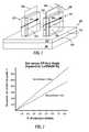
- FIG. 2is a plot of the reduction in transconductance in the linear and saturation region of a FinFET vs. off angle axis ⁇ ;
- FIG. 3Ais a top view and FIG. 3B is a side view through line 3 B- 3 B of FIG. 3A of a FinFET transistor according to the first embodiment of the present invention
- FIG. 4Ais a top view and FIG. 4B is a side view through line 4 B- 4 B of FIG. 4A of a FinFET transistor according to a second embodiment of the present invention
- FIG. 5is an exemplary circuit utilizing a FinFET whose drive strength has been tuned according to the first embodiment of the present invention.
- FIG. 6is an exemplary circuit utilizing a FinFET whose drive strength has been tuned according to the second embodiment of the present invention.
- crystalline solidsthe atoms, which make up the solid, are spatially arranged in a periodic fashion called a lattice.
- a crystal latticealways contains a volume, which is representative of the entire lattice and is regularly repeated throughout the crystal.
- the directions in a latticeare expressed as a set of three integers with the same relationship as the components of a vector in that direction.
- cubic latticessuch as silicon, which have a diamond crystal lattice
- a body diagonalexists along the [111] direction with the [ ] brackets denoting a specific direction.
- Many directions in a crystal latticeare equivalent by a symmetry transformation, depending upon the arbitrary choice of orientation axes.
- a crystal directions in the cubic lattice [100], [010] and [001]are all crystallographically equivalent.
- a direction and all its equivalent directionsare denoted by ⁇ > brackets.
- the designation of the ⁇ 100> directionincludes the equivalent [100], [010] and [001] positive directions as well as the equivalent negative directions [ ⁇ 100], [0-10] and [00-1].
- Planes in a crystalmay also be identified with a set of three integers. They are used to define a set of parallel planes and each set of integers enclosed in ( ) parentheses identifies a specific plane. For example the proper designation for a plane perpendicular to the [100] direction is (100). Thus, if either a direction or a plane of a cubic lattice is known, its perpendicular counterpart may be quickly determined without calculation. Many planes in a crystal lattice are equivalent by a symmetry transformation, depending upon the arbitrary choice of orientation axes. For example, the (100), (010) and (001) planes are all crystallographically equivalent. A plane and all its equivalent planes are denoted by ⁇ ⁇ parentheses. Thus, the designation of the ⁇ 100 ⁇ plane includes the equivalent (100), (010) and (001) positive planes as well as the equivalent planes ( ⁇ 100), (0-10) and (00-1).
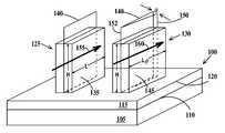
- FIG. 1is an isometric view of representative fin portions of various FinFETs according to the various embodiments of the present invention.
- a substrate 100includes a support layer 105 having a top surface 110 , an isolation layer 115 having a top surface 120 , the isolation layer formed on top surface 110 of support layer 105 .
- Isolation layer 115may comprise a buried oxide layer (BOX), or may comprise a doped semiconductor region.
- Fins 125 and 130are formed from a crystalline semiconductor material formed on top surface 120 of buried isolation 115 . Fins 125 and 130 may be composed of any appropriate semiconductor material, including, but not limited to: Si, Ge, GaP, InAs, InP, SiGe, GaAs, or other group III/V compounds.
- Fin 125has parallel sidewalls 135 (only one sidewall is visible in FIG. 1 ) parallel to a crystal-plane 140 .
- Fin 130has parallel sidewalls 145 (only one sidewall is visible in FIG. 1 ) parallel to a crystal-plane 150 .
- Plane 150is offset from crystal-plane 140 by an angle ⁇ with respect to a common axis 152 .
- fins 125 and 130when used in an NFET FinFET (hereafter N FinFET) comprise single-crystal silicon and crystal-plane 140 is a ⁇ 100 ⁇ crystal-plane and when used in a PFET FinFET (hereafter P FinFET), comprise single-crystal silicon and crystal-plane 140 is a ⁇ 110 ⁇ crystal-plane.
- N FinFETNFET FinFET
- P FinFETPFET FinFET
- Fin 125has a physical length L in a direction parallel to top surface 120 of buried isolation layer 115 within plane 140 and a physical height H in a direction perpendicular to the direction of physical length L.
- Fin 130has a physical length L ⁇ in a direction parallel to top surface 120 of buried isolation layer 115 within a plane 150 (which is offset from plane 140 by angle ⁇ ) and a physical height H in a direction perpendicular to the direction of physical length Le.
- the physical height of the findetermines the electrical channel width of the transistor.
- the physical height Hdetermines the electrical channel width W.
- the channel widthis twice the height because there is a gate on either side of the fin, W is a function of 2H. (See definition of a double-gate FinFET infra).
- the physical length of a FinFET findefines the channel length of FinFET the same as for conventional FETs, thus the designation L or L ⁇ may be understood to also mean channel length hereafter.
- inversion carrier flow directionis in directions 155 and 160 respectively.
- Direction 155is parallel to sidewalls 135 and direction 160 is parallel to sidewalls 145 .
- inversion carrier flowis affected by the crystal orientation of the fin of a FinFET.
- maximum inversion carrier (electron) mobilityis along the ⁇ 100 ⁇ crystal-plane and for P FinFETs the maximum inversion carrier (hole) mobility is along the ⁇ 110 ⁇ crystal-plane. This is reflected in the transconductance (Gm) of a FinFET as illustrated in FIG. 2 and discussed infra.
- FIG. 2is a plot of the reduction in transconductance in the linear and saturation region of a FinFET vs. off angle axis ⁇ .
- Transconductance(Gm) is the ratio of output current to input voltage and is the measure of the gain of a FET.
- Gm linupper curve
- Gm satsaturation region
- the curves of FIG. 2may be explained, in at least part, by the following:
- the mobility of the electrons (inversion carriers) in the channels of NFETsis nearly at its highest in the ⁇ 100 ⁇ plane and significantly lower in the ⁇ 110 ⁇ plane.
- the electron-mobility in the ⁇ 110 ⁇ planeis about half that in the ⁇ 100 ⁇ plane.
- the mobility of holes (inversion carriers) in the channels of PFETsis highest in the ⁇ 110 ⁇ plane and significantly lower in the ⁇ 100 ⁇ plane.
- the hole-mobility in the ⁇ 100 ⁇ planeis about less than half that in the ⁇ 110 ⁇ plane.
- the ⁇ 100 ⁇ and ⁇ 110 ⁇ planesare orientated to each other at an angle of 45° when formed by vertical surfaces cut from a ⁇ 100 ⁇ -surfaced wafer.
- FIG. 3Ais a top view and FIG. 3B is a side view through line 3 B- 3 B of FIG. 3A of a FinFET transistor according to the first embodiment of the present invention.
- FinFET 200includes parallel source/drains 205 A and 205 B in physical and electrical contact with opposite ends of single-crystal peipendicular fins 210 and an angled single-crystal fin 215 .
- Perpendicular fins 210are longitudinally aligned with a plane 220
- angled fin 215is longitudinally aligned with a plane 225 , which is offset (by rotation along a axis common to both planes 210 and 225 as illustrated in FIG.
- Fins 210are perpendicular to source/drains 205 A and 205 B.
- a common gate 230is formed over perpendicular fins 210 and angled fin 215 and is electrically isolated from the fins by gate dielectric 235 formed on opposite sides of each fin.
- Perpendicular fins 210 and angled fin 215have the same height H (see FIG. 3B ).
- perpendicular fins 210 and angled fin 215have a height H and top surfaces 235 of perpendicular fins 210 and top surface 237 of angled fin 215 are electrically isolated from gate 230 by dielectric caps 240 . Note, it is possible to replace dielectric caps 240 with gate dielectric 230 .
- Perpendicular fins 210 and angled fin 215are formed on a top surface 245 of an insulating layer 250 , which is formed on a top surface 255 of a substrate 260 .
- FinFET 200is an N FinFET
- source/drains 205 A and 205 Bare doped N-type
- perpendicular fins 210 and angled fin 215comprises comprise P-doped, lightly N-doped or intrinsic mono-crystalline silicon
- plane 220is a ⁇ 100 ⁇ crystal-plane and ⁇ is an angle of rotation into the ⁇ 101 ⁇ crystal-plane.
- FinFET 200is a P FinFET
- source/drains 205 A and 205 Bare doped P-type
- perpendicular fins 210 and angled fin 215comprise N-doped, or lightly P-doped or intrinsic mono-crystalline silicon
- plane 220is a ⁇ 110 ⁇ crystal-plane and ⁇ is an angle of rotation into the ⁇ 100 ⁇ crystal-plane.
- lightly doped N or P monocrystalline siliconhas having a doping level that will not prevent formation of a inversion layer in the channel region under the gate of the fin between the source and drains of a FinFET with a normal operating voltage applied to the gate.
- lightly doped siliconhas an N or P dopant species concentration of about 10 15 atm/cm 3 or less.
- the drive strength of a transistoris defined as the measure of the amount of current the transistor can supply.
- the ratio of drive strengths between PFETS and NFETS in integrated circuitsis an important consideration as will be described infra.
- the relative drive strength of FinFET 200is given in equation 1. ⁇ ( W/L )(3+(cos ⁇ )(1 ⁇ 0.9(
- ⁇the relative drive strength of the transistor
- Nthe number pf perpendicular fins
- Mthe number of angled fins
- Wthe channel width of each fin
- Lthe length of the perpendicular fins
- ⁇the angle between the perpendicular fins and the angled fin, in degrees.
- the granularity of control of drive strengthis related to the number of fins and is very coarse unless there are a prohibitive number of fins.
- the drive strength of a FinFET incorporating at least one perpendicular fin and one angled fincan be adjusted by not only the total number of fins of each type, but by the angle of the angled fin(s) relative to the perpendicular fin. This degree of tuning is only limited by the incremental control of the process in imaging incremental changes in fin angle ( ⁇ ) and the minimum reduction (about 0.5) at a corresponding maximum angle (about 45°) in carrier mobility that can be realized. Increments below about 0.5 can be obtained with multiple angled fins. See Table I.
- a double-gate transistoris defined as a transistor having two dependent gates, in the case of a FinFET, the gates are located on opposing sidewalls of the fin and electrically connected. They may be integral to one another as well, as is illustrated in FIGS. 4A and 4B .
- a split-gate transistoris defined as a transistor having two independent gates, in the case of a FinFET, the gates are located on opposing sidewalls of the fin and are electrically isolated from one another.
- FIG. 4Ais a top view and FIG. 4B is a side view through line 4 B- 4 B of FIG. 4A of a FinFET transistor according to a second embodiment of the present invention.
- FinFET 300includes parallel source/drains 305 A and 305 B in physical and electrical contact with opposite ends of single-crystal double-gate fins 310 and a single-crystal split-gate fin 315 .
- Double-gate fins 310 and split-gate fin 315are longitudinally aligned with mutually parallel planes 320 .
- Planes 320may be higher inversion carrier mobility planes, for example ⁇ 100 ⁇ for N FinFETs and ⁇ 110 ⁇ for P FinFETs.
- Double-gate fins 310 and split-gate fin 315are perpendicular to source/drains 305 A and 305 B.
- a gate dielectric 330is formed on sidewalls of double-gate fins 310 and split-gate fin 315 .
- a first gate 335is formed over double-gate fins 310 and contacts gate dielectric 330 on formed on both sidewalls of each double-gate fin 315 .
- First gate 335also contacts gate dielectric 330 formed on a first side 340 A of split-gate fin 315 .
- a second gate 345contacts gate dielectric 330 formed on a second side of split-gate fin 315 .
- Double-gate fins 305 A and split-gate fin 315have the same channel length L and have the same height H (see FIG. 4B ).
- double-gate fins 310 and split-gate fin 315have a height H and top surfaces 350 of double-gate fins 310 are electrically isolated from first gate 335 by dielectric caps 355 .
- a dielectric cap 365is formed on a top surface 360 of split-gate fin 315 . Note, it is possible to replace dielectric caps 355 and 365 with gate dielectric 330 .
- Double-gate fins 310 and split-gate fin 315are formed on a top surface 370 of an insulating layer 375 , which is formed on a top surface 380 of a substrate 385 .
- FinFET 300is an N FinFET
- source/drains 305 A and 305 Bare doped N-type
- double-gate fins 310 and split-gate fin 315comprise P-doped, lightly N-doped or intrinsic mono-crystalline silicon
- plane 320has ⁇ 100 ⁇ orientation.
- FinFET 300is a P FinFET
- source/drains 305 A and 3105 Bare doped P-type
- double-gate fins 310 and split-gate fin 315comprise N-doped, lightly P-doped, or intrinsic mono-crystalline silicon
- plane 320is a ⁇ 110 ⁇ crystal-plane
- the drive strength contribution of split-gate fin 315 with zero voltage on second gate 345is about half that of a double-gate fin 310 .
- the drive strength contribution of split-gate fin 315can be varied between about zero to the same as that of double-gate fins 310 by varying the voltage applied to second gate 345 .
- FIGS. 4A and 4Bthere may be any number from one upward of double-gate fins 310 and any number from one upward of split-gate fins 315 .
- the two outermost fins of a set of finsmay very easily be fabricated as split-gate fins.
- Inner finsmay be formed as split-gate fins, but more complicated gate shape layouts (when viewed in top or plan view) are required.
- the drive strength ratio(also called the Beta-ratio) is the quotient given by the effective channel width-to-length (W/L) ratio of the PFET divided by the effective channel width-to-length (W/L) ratio of the NFET.
- the FinFET transistors described supra,allow fine-tuning of the Beta-ratio.
- transistors bodiesare formed from one of more mono-crystalline fins, thus in the description of FIGS. 5 and 6 , the term fin can be read as body as well.
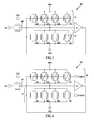
- FIG. 5is an exemplary circuit utilizing a FinFET whose drive strength has been tuned according to the first embodiment of the present invention.
- a latch circuit 400includes transistors T 1 , T 2 , T 3 and an inverter I 1 .
- Transistors T 1 , T 2 and T 3are double-gate FinFET transistors.
- Transistor T 1is illustrated as an N FinFET having a one fin 405 .
- Transistor T 2is illustrated as an N FinFET having three perpendicular fins 410 and one angle fin 415 and a common gate. Angled fin 410 is also designated with the symbol ⁇ .
- Transistor T 3is illustrated as a P FinFET having four perpendicular fins 420 and a common gate.
- the source of transistor T 1is coupled to an input signal, the gate of transistor T 1 is coupled to a CLK signal and the drain of transistor T 1 is coupled to the gates of transistors T 2 and T 3 , the drains of transistors T 2 and T 3 and the input and output of inverter I 1 .
- the source of transistor T 3is coupled to VDD and the source of transistor T 2 is coupled to VSS.
- the drive strength ratio(also known as the beta ratio), ⁇ T3 / ⁇ T2 of latch circuit 400 can be tuned (in the sense of set during manufacture of the circuit) by rotation of fin 415 of transistor T 2 in a direction relative to the direction of fins 410 that reduces the mobility of the inversion carriers in fin 415 relative to the mobility of the inversion carriers in fins 410 .
- transistor T 2is illustrated in FIG. 5 and described as being drive strength tunable, either or both of transistors T 2 or T 3 may be drive strength tunable according to the first embodiment of the present invention.
- FIG. 6is an exemplary circuit utilizing a FinFET whose drive strength has been tuned according to the second embodiment of the present invention.
- a latch circuit 450includes transistors T 4 , T 5 , T 6 and an inverter I 2 .
- Transistor T 4is a double-gate FinFET transistor.
- Transistors T 5 and T 6are mixed gate FinFET transistors having multiple double-gate fins and one split-gate fin each.
- Transistor T 4is illustrated as an N FinFET having one double-gate fin 455 .
- Transistor T 5is illustrated as an N FinFET having three fins 460 and one fin 465 , a first gate common to all gate regions of fins 460 and a first gate region of fin 465 , and a second gate connected only to a second gate region of fin 465 .
- Transistor T 6is illustrated as a P FinFET having three fins 470 and one fin 475 , a first gate common to all gate regions of fins 470 and a first gate region of fin 475 , and a second gate connected only to a second gate region of fin 475 .
- the source of transistor T 4is coupled to an input signal, the gate of transistor T 4 is coupled to a CLK signal and the drain of transistor T 4 is coupled to the first gates of transistors T 5 and T 6 , the drains of transistors T 5 and T 6 and the input and output of inverter I 2 .
- the second gate of transistor T 5is coupled to a voltage source VTUNE-N and the second gate of transistor T 6 is coupled to a voltage source VTUNE-P.
- the source of transistor T 6is coupled to VDD and the source of transistor T 5 is coupled to VSS.
- transistors T 5 and T 6are illustrated as having tunable drive strength transistors, only one of transistors T 5 or T 6 need be drive strength tunable according to the second embodiment of the present invention.
- SRAMstatic random access memory
- PLLphase locked loop
- CMOS logic circuitsdynamic domino circuits
- imbalanced static combinational CMOS logic circuitsimbalanced static combinational CMOS logic circuits.
- the present inventionprovides fine-tunable drive strength FinFETs and methods for fine-tuning the drive strength of FinFETs.
- the entire angled finneed not be set at an angle relative to the perpendicular fin, but may be bent so a portion of the angled fin is parallel to the perpendicular fin and a portion angled relative to the perpendicular fin. Therefore, it is intended that the following claims cover all such modifications and changes as fall within the true spirit and scope of the invention.
Landscapes
- Metal-Oxide And Bipolar Metal-Oxide Semiconductor Integrated Circuits (AREA)
- Thin Film Transistor (AREA)
- Insulated Gate Type Field-Effect Transistor (AREA)
Abstract
Description
- This application is a continuation of copending U.S. patent application Ser. No. 11/458,250 filed on Jul. 18, 2006 which is a divisional application of U.S. patent application Ser. No. 10/709,076 filed on Apr. 12, 2006, now U.S. Pat. No. 7,115,929 issued on Dec. 3, 2006.
- The present invention relates to the field of FinFET (fin field effect transistors); more specifically, it relates to FinFETs with tuned drive strength, methods tuning the drive strength of FinFETs and circuits utilizing FinFETs with tuned drive strengths.
- Integrated circuit technology and complementary metal-oxide-silicon (CMOS) technology is ever pushed in the direction of higher performance and hence smaller transistor dimensions. Below about 65 nm FinFET technology is emerging as the technology to carry forward the pursuit of high performance circuits. At the high performance levels utilizing sub-65 nm dimensions, very fine tuning the drive strengths of transistors in integrated circuits becomes critical, however, no method presently exists for doing this for circuits made up of FinFETs because of the quantized nature of their structures. Thus, there is a need for fine tunable drive strength FinFETs and methods of fine-tuning the drive strength of FinFETs.
- A first aspect of the present invention is an electronic device, comprising: a source and a drain; a single-crystal first fin having first and second opposing ends and first and second opposing sidewalls and extending along a first longitudinal axis from the first to the second end of the first fin, the first end of the first fin in contact with the source and the second end of the first fin in contact with the drain, the first longitudinal axis aligned to a crystal plane; a single-crystal second fin having first and second opposing ends and first and second opposing sidewalls and extending along a second longitudinal axis from the first to the second end of the second fin, the first end of the second fin in contact with the source and the second end of the second fin in contact with the drain, the second longitudinal axis aligned in a plane rotated away from the crystal plane; and a single conductive gate in contact with a gate dielectric formed on the first and second sidewalls of the first fin and on the first and second sidewalls of the second fin.
- A second aspect of the present invention is a method for tuning the drive strength of an electronic device, comprising: forming a source and a drain in a single-crystal material; forming a single-crystal first fin from the single-crystal material, the first fin having first and second opposing ends and first and second opposing sidewalls and extending along a first longitudinal axis from the first to the second end of the first fin, the first end of the first fin in contact with the source and the second end of the first fin in contact with the drain; aligning the first longitudinal axis to a crystal-plane of the single-crystal material; forming a single-crystal second fin from the single-crystal material, the second fin having first and second opposing ends and first and second opposing sidewalls and extending along a second longitudinal axis from the first to the second end of the second fin, the first end of the second fin in contact with the source and the second end of the second fin in contact with the drain; aligning the second longitudinal axis to a plane rotated away from the crystal plane; and providing a conductive gate in contact with a gate dielectric formed on the first and second sidewalls of the first fin and on the first and second sidewalls of the second fin.
- A third aspect of the present invention an integrated circuit, comprising: a first transistor comprising: a first source and a first drain; a single-crystal first fin having first and second opposing ends and first and second opposing sidewalls and extending along a first longitudinal axis from the first to the second end of the first fin, the first end of the first fin in contact with the first source and the second end of the first fin in contact with the first drain, the first longitudinal axis aligned to a crystal plane; a single-crystal second fin having first and second opposing ends and first and second opposing sidewalls and extending along a second longitudinal axis from the first to the second end of the second fin, the first end of the second fin in contact with the first source and the second end of the second fin in contact with the first drain, the second longitudinal axis aligned in a plane rotated away from the crystal plane; and a first conductive gate in contact with a gate dielectric formed on the first and second sidewalls of the first fin and on the first and second sidewalls of the second fin; and a second transistor comprising: a second source and a second drain; a single-crystal third fin having first and second opposing ends and first and second opposing sidewalls and extending along a third longitudinal axis from the first to the second end of the third fin, the first end of the third fin in contact with the second source and the second end of the first fin in contact with the second drain, the third longitudinal axis aligned to the crystal plane; and a second conductive gate in contact with a gate dielectric formed on the first and second sidewalls of the third fin and on the first and second sidewalls of the third fin.
- A fourth aspect of the present invention is a method of tuning the drive strength ratio between a first transistor and a second transistor in an integrated circuit, comprising: providing the first transistor, the first transistor comprising: a first source and a first drain; a single-crystal first fin having first and second opposing ends and first and second opposing sidewalls and extending along a first longitudinal axis from the first to the second end of the first fin, the first end of the first fin in contact with the first source and the second end of the first fin in contact with the first drain, the first longitudinal axis aligned to a crystal plane; a single-crystal second fin having first and second opposing ends and first and second opposing sidewalls and extending along a second longitudinal axis from the first to the second end of the second fin, the first end of the second fin in contact with the first source and the second end of the second fin in contact with the first drain, the second longitudinal axis aligned in a plane rotated away from the crystal plane; and a first conductive gate in contact with a gate dielectric formed on the first and second sidewalls of the first fin and on the first and second sidewalls of the second fin; and providing the second transistor, the second transistor comprising: a second source and a second drain; a single-crystal third fin having first and second opposing ends and first and second opposing sidewalls and extending along a third longitudinal axis from the first to the second end of the third fin, the first end of the third fin in contact with the second source and the second end of the first fin in contact with the second drain, the third longitudinal axis aligned to the crystal plane; and a second conductive gate in contact with a gate dielectric formed on the first and second sidewalls of the third fin and on the first and second sidewalls of the third fin.
- A fifth aspect of the present invention is an electronic device, comprising: a source and a drain; a single-crystal first fin having first and second opposing ends and first and second opposing sidewalls, the first end of the first fin in contact with the source and the second end of the first fin in contact with the drain, the first longitudinal axis aligned to a crystal plane; a single-crystal second fin having first and second opposing ends and first and second opposing sidewalls, the first end of the second fin in contact with the source and the second end of the second fin in contact with the drain; a first conductive gate in contact with a gate dielectric formed on the first and second sidewalls of the first fin and on the first sidewall of the second fin; and a second conductive gate in contact with a gate dielectric formed on the second sidewall of the second fin.
- A sixth aspect of the present invention is a method for tuning the drive strength of an electronic device, comprising: providing a source and a drain, providing a single-crystal first fin having first and second opposing ends and first and second opposing sidewalls, the first end of the first fin in contact with the source and the second end of the first fin in contact with the drain; providing a single-crystal second fin having first and second opposing ends and first and second opposing sidewalls, the first end of the second fin in contact with the source and the second end of the second fin in contact with the drain; providing a first conductive gate in contact with a gate dielectric formed on the first and second sidewalls of the first fin and on the first sidewall of the second fin; providing a second conductive gate in contact with a gate dielectric formed on the second sidewall of the second fin; and connecting the first gate to a first voltage source at a first voltage level and connecting the second gate a second voltage source at a second voltage level, the first and second voltage levels being different.
- A seventh aspect of the present invention is an integrated circuit, comprising: a first transistor comprising: a first source and a first drain; a single-crystal first fin having first and second opposing ends and first and second opposing sidewalls, the first end of the first fin in contact with the first source and the second end of the first fin in contact with the first drain; a single-crystal second fin having first and second opposing ends and first and second opposing sidewalls, the first end of the second fin in contact with the first source and the second end of the second fin in contact with the first drain; a first conductive gate in contact with a gate dielectric formed on the first and second sidewalls of the first fin and on the first sidewall of the second fin; and a second conductive gate in contact with a gate dielectric formed on the second sidewall of the second fin; and a second transistor comprising: a second source and a second drain; a single-crystal third fin having first and second opposing ends and first and second opposing sidewalls, the first end of the third fin in contact with the second source and the second end of the third fin in contact with the second drain; and a third conductive gate in contact with a gate dielectric formed on the first and second sidewalls of the third fin and on the first and second sidewall of the third fin.
- An eighth aspect of the present invention is a method of tuning the drive strength ratio between a first transistor and a second transistor in an integrated circuit, comprising providing the first transistor, the first transistor comprising: a first source and a first drain; a single-crystal first fin having first and second opposing ends and first and second opposing sidewalls, the first end of the first fin in contact with the first source and the second end of the first fin in contact with the first drain; a single-crystal second fin having first and second opposing ends and first and second opposing sidewalls, the first end of the second fin in contact with the first source and the second end of the second fin in contact with the first drain; a first conductive gate in contact with a gate dielectric formed on the first and second sidewalls of the first fin and on the first sidewall of the second fin; and a second conductive gate in contact with a gate dielectric formed on the second sidewall of the second fin; providing the second transistor, the second transistor comprising: a second source and a second drain; a single-crystal third fin having first and second opposing ends and first and second opposing sidewalls, the first end of the third fin in contact with the second source and the second end of the third fin in contact with the second drain; and a third conductive gate in contact with a gate dielectric formed on the first and second sidewalls of the third fin and on the first and second sidewall of the third fin; and connecting the first gate to a first voltage source at a first voltage level and connecting the second gate to a second voltage source at a second voltage level, the first and second voltage levels being different.
- The features of the invention are set forth in the appended claims. The invention itself, however, will be best understood by reference to the following detailed description of an illustrative embodiment when read in conjunction with the accompanying drawings, wherein:
FIG. 1 is an isometric view of representative fin portions of various FinFETs according to the various embodiments of the present invention;FIG. 2 is a plot of the reduction in transconductance in the linear and saturation region of a FinFET vs. off angle axis θ;FIG. 3A is a top view andFIG. 3B is a side view throughline 3B-3B ofFIG. 3A of a FinFET transistor according to the first embodiment of the present invention;FIG. 4A is a top view andFIG. 4B is a side view throughline 4B-4B ofFIG. 4A of a FinFET transistor according to a second embodiment of the present invention;FIG. 5 is an exemplary circuit utilizing a FinFET whose drive strength has been tuned according to the first embodiment of the present invention; andFIG. 6 is an exemplary circuit utilizing a FinFET whose drive strength has been tuned according to the second embodiment of the present invention.- In crystalline solids, the atoms, which make up the solid, are spatially arranged in a periodic fashion called a lattice. A crystal lattice always contains a volume, which is representative of the entire lattice and is regularly repeated throughout the crystal. In describing crystalline semiconductor materials in the present disclosure, the following conventions are used.
- The directions in a lattice are expressed as a set of three integers with the same relationship as the components of a vector in that direction. For example, in cubic lattices, such as silicon, which have a diamond crystal lattice, a body diagonal exists along the [111] direction with the [ ] brackets denoting a specific direction. Many directions in a crystal lattice are equivalent by a symmetry transformation, depending upon the arbitrary choice of orientation axes. For example, a crystal directions in the cubic lattice [100], [010] and [001] are all crystallographically equivalent. A direction and all its equivalent directions are denoted by < > brackets. Thus, the designation of the <100> direction includes the equivalent [100], [010] and [001] positive directions as well as the equivalent negative directions [−100], [0-10] and [00-1].
- Planes in a crystal may also be identified with a set of three integers. They are used to define a set of parallel planes and each set of integers enclosed in ( ) parentheses identifies a specific plane. For example the proper designation for a plane perpendicular to the [100] direction is (100). Thus, if either a direction or a plane of a cubic lattice is known, its perpendicular counterpart may be quickly determined without calculation. Many planes in a crystal lattice are equivalent by a symmetry transformation, depending upon the arbitrary choice of orientation axes. For example, the (100), (010) and (001) planes are all crystallographically equivalent. A plane and all its equivalent planes are denoted by { } parentheses. Thus, the designation of the {100} plane includes the equivalent (100), (010) and (001) positive planes as well as the equivalent planes (−100), (0-10) and (00-1).
FIG. 1 is an isometric view of representative fin portions of various FinFETs according to the various embodiments of the present invention. InFIG. 1 , asubstrate 100 includes asupport layer 105 having atop surface 110, anisolation layer 115 having atop surface 120, the isolation layer formed ontop surface 110 ofsupport layer 105.Isolation layer 115 may comprise a buried oxide layer (BOX), or may comprise a doped semiconductor region. Fins125 and130 are formed from a crystalline semiconductor material formed ontop surface 120 of buriedisolation 115. Fins125 and130 may be composed of any appropriate semiconductor material, including, but not limited to: Si, Ge, GaP, InAs, InP, SiGe, GaAs, or other group III/V compounds.Fin 125 has parallel sidewalls135 (only one sidewall is visible inFIG. 1 ) parallel to a crystal-plane 140.Fin 130 has parallel sidewalls145 (only one sidewall is visible inFIG. 1 ) parallel to a crystal-plane 150.Plane 150 is offset from crystal-plane 140 by an angle θ with respect to acommon axis 152. In one example,fins plane 140 is a {100} crystal-plane and when used in a PFET FinFET (hereafter P FinFET), comprise single-crystal silicon and crystal-plane 140 is a {110} crystal-plane. In one example, whencrystal plane 140 is a {100} crystal-plane, θ defines a rotation offin 130 into the {110} crystal-plane and whencrystal plane 140 is a {110} crystal-plane, θ defines a rotation offin 140 into the {100} crystal-plane.Fin 125 has a physical length L in a direction parallel totop surface 120 of buriedisolation layer 115 withinplane 140 and a physical height H in a direction perpendicular to the direction of physicallength L. Fin 130 has a physical length Lθ in a direction parallel totop surface 120 of buriedisolation layer 115 within a plane150 (which is offset fromplane 140 by angle θ) and a physical height H in a direction perpendicular to the direction of physical length Le. Note, in a FinFET, the physical height of the fin determines the electrical channel width of the transistor. In a single gate FinFET (a gate formed on one side of the fin) the physical height H determines the electrical channel width W. In a double-gate FinFET the channel width is twice the height because there is a gate on either side of the fin, W is a function of 2H. (See definition of a double-gate FinFET infra). The physical length of a FinFET fin defines the channel length of FinFET the same as for conventional FETs, thus the designation L or Lθ may be understood to also mean channel length hereafter.- When
fins directions Direction 155 is parallel to sidewalls135 anddirection 160 is parallel to sidewalls145. It is well known, that inversion carrier flow is affected by the crystal orientation of the fin of a FinFET. For N FinFETs, maximum inversion carrier (electron) mobility is along the {100} crystal-plane and for P FinFETs the maximum inversion carrier (hole) mobility is along the {110} crystal-plane. This is reflected in the transconductance (Gm) of a FinFET as illustrated inFIG. 2 and discussed infra. FIG. 2 is a plot of the reduction in transconductance in the linear and saturation region of a FinFET vs. off angle axis θ. Transconductance (Gm) is the ratio of output current to input voltage and is the measure of the gain of a FET. InFIG. 2 both the transconductance when the transistor is operating in the linear region Gm lin (upper curve) and the transconductance when the transistor is operating in the saturation region Gm sat (lower curve) are only equal at θ (offset from the maximum mobility axis)=0. Gm sat progressively fails off from Gm lin as θ increases.- The curves of
FIG. 2 may be explained, in at least part, by the following: The mobility of the electrons (inversion carriers) in the channels of NFETs is nearly at its highest in the {100} plane and significantly lower in the {110} plane. The electron-mobility in the {110} plane is about half that in the {100} plane. The mobility of holes (inversion carriers) in the channels of PFETs is highest in the {110} plane and significantly lower in the {100} plane. The hole-mobility in the {100} plane is about less than half that in the {110} plane. The {100} and {110} planes are orientated to each other at an angle of 45° when formed by vertical surfaces cut from a {100}-surfaced wafer. FIG. 3A is a top view andFIG. 3B is a side view throughline 3B-3B ofFIG. 3A of a FinFET transistor according to the first embodiment of the present invention. InFIG. 3A ,FinFET 200 includes parallel source/drains205A and205B in physical and electrical contact with opposite ends of single-crystal peipendicular fins 210 and an angled single-crystal fin 215.Perpendicular fins 210 are longitudinally aligned with aplane 220, whileangled fin 215 is longitudinally aligned with aplane 225, which is offset (by rotation along a axis common to bothplanes FIG. 1 and described supra) fromcrystal plane 220 by an angle θ. The angle θ also represents a rotation from a higher inversion carrier mobility direction to a lower major carrier mobility direction.Fins 210 are perpendicular to source/drains205A and205B. Acommon gate 230 is formed overperpendicular fins 210 andangled fin 215 and is electrically isolated from the fins bygate dielectric 235 formed on opposite sides of each fin.Perpendicular fins 210 have a channel length L andangled fin 215 has a channel length Lθ where Lθ=L/cos θ.Perpendicular fins 210 andangled fin 215 have the same height H (seeFIG. 3B ).- Turning to
FIG. 3B , it can be seen thatperpendicular fins 210 andangled fin 215 have a height H andtop surfaces 235 ofperpendicular fins 210 andtop surface 237 ofangled fin 215 are electrically isolated fromgate 230 bydielectric caps 240. Note, it is possible to replacedielectric caps 240 withgate dielectric 230.Perpendicular fins 210 andangled fin 215 are formed on atop surface 245 of an insulatinglayer 250, which is formed on atop surface 255 of asubstrate 260. - In a first example,
FinFET 200 is an N FinFET, source/drains205A and205B are doped N-type,perpendicular fins 210 andangled fin 215 comprises comprise P-doped, lightly N-doped or intrinsic mono-crystalline silicon,plane 220 is a {100} crystal-plane and θ is an angle of rotation into the {101} crystal-plane. In a second example,FinFET 200 is a P FinFET, source/drains205A and205B are doped P-type,perpendicular fins 210 andangled fin 215 comprise N-doped, or lightly P-doped or intrinsic mono-crystalline silicon,plane 220 is a {110} crystal-plane and θ is an angle of rotation into the {100} crystal-plane. - Lightly doped N or P monocrystalline silicon is defined has having a doping level that will not prevent formation of a inversion layer in the channel region under the gate of the fin between the source and drains of a FinFET with a normal operating voltage applied to the gate. In one example, lightly doped silicon has an N or P dopant species concentration of about 1015atm/cm3or less.
- The drive strength of a transistor is defined as the measure of the amount of current the transistor can supply. The ratio of drive strengths between PFETS and NFETS in integrated circuits is an important consideration as will be described infra. The relative drive strength of
FinFET 200 is given inequation 1.
β≈(W/L)(3+(cos θ)(1−0.9(|θ/45°|))), |θ|<45° (1)
where:
β=the relative drive strength of the transistor;
W=the channel width of each fin;
L=the length of the three perpendicular fins205; and
θ=the angle between the three perpendicular fins and the angled fin. - While three
perpendicular fins 210 and oneangled fin 215 are illustrated inFIGS. 3A and 3B , there may be any number from one upward ofperpendicular fins 210 and any number from one upward ofangled fins 215. There must be at least oneperpendicular fin 210 and oneangled fin 215. In the general case, of Nperpendicular fins 210 and M angledfins 215 the relative drive strength of the general case tunable drive strength FinFET is given in equation 2.
β(W/L)(N+Mcos(θ)(1−0.9(|θ/45°|))), |θ|<45° (2)
where:
β=the relative drive strength of the transistor;
N=the number pf perpendicular fins;
M=the number of angled fins;
W=the channel width of each fin;
L=the length of the perpendicular fins; and
θ=the angle between the perpendicular fins and the angled fin, in degrees. - In a FinFET using only perpendicular fins the granularity of control of drive strength is related to the number of fins and is very coarse unless there are a prohibitive number of fins. The drive strength of a FinFET incorporating at least one perpendicular fin and one angled fin can be adjusted by not only the total number of fins of each type, but by the angle of the angled fin(s) relative to the perpendicular fin. This degree of tuning is only limited by the incremental control of the process in imaging incremental changes in fin angle (θ) and the minimum reduction (about 0.5) at a corresponding maximum angle (about 45°) in carrier mobility that can be realized. Increments below about 0.5 can be obtained with multiple angled fins. See Table I.
TABLE I Drive Strength Number Angle Between (Multiples of Perpendicular Number of Perpendicular W/L) Fins Angled Fins and Angled Fins 3 3 0 N/A 4 4 0 N/A 3.8 3 1 ˜10° 3.2 2 2 ˜10° - Before describing the second embodiment of the present invention the terms double-gate and split-gate need to be defined. A double-gate transistor is defined as a transistor having two dependent gates, in the case of a FinFET, the gates are located on opposing sidewalls of the fin and electrically connected. They may be integral to one another as well, as is illustrated in
FIGS. 4A and 4B . A split-gate transistor is defined as a transistor having two independent gates, in the case of a FinFET, the gates are located on opposing sidewalls of the fin and are electrically isolated from one another. FIG. 4A is a top view andFIG. 4B is a side view throughline 4B-4B ofFIG. 4A of a FinFET transistor according to a second embodiment of the present invention. InFIG. 4A ,FinFET 300 includes parallel source/drains305A and305B in physical and electrical contact with opposite ends of single-crystal double-gate fins 310 and a single-crystal split-gate fin 315.Double-gate fins 310 andsplit-gate fin 315 are longitudinally aligned with mutuallyparallel planes 320.Planes 320 may be higher inversion carrier mobility planes, for example {100} for N FinFETs and {110} for P FinFETs.Double-gate fins 310 andsplit-gate fin 315 are perpendicular to source/drains305A and305B. Agate dielectric 330 is formed on sidewalls ofdouble-gate fins 310 andsplit-gate fin 315. Afirst gate 335 is formed overdouble-gate fins 310 andcontacts gate dielectric 330 on formed on both sidewalls of eachdouble-gate fin 315.First gate 335 also contacts gate dielectric330 formed on afirst side 340A ofsplit-gate fin 315. Asecond gate 345 contacts gate dielectric330 formed on a second side ofsplit-gate fin 315.Double-gate fins 305A andsplit-gate fin 315 have the same channel length L and have the same height H (seeFIG. 4B ).- Turning to
FIG. 4B , it can be seen thatdouble-gate fins 310 andsplit-gate fin 315 have a height H andtop surfaces 350 ofdouble-gate fins 310 are electrically isolated fromfirst gate 335 bydielectric caps 355. Adielectric cap 365 is formed on atop surface 360 ofsplit-gate fin 315. Note, it is possible to replacedielectric caps gate dielectric 330.Double-gate fins 310 andsplit-gate fin 315 are formed on atop surface 370 of an insulatinglayer 375, which is formed on atop surface 380 of asubstrate 385. - In a first example,
FinFET 300 is an N FinFET, source/drains305A and305B are doped N-type,double-gate fins 310 andsplit-gate fin 315 comprise P-doped, lightly N-doped or intrinsic mono-crystalline silicon, andplane 320 has {100} orientation. In a second example,FinFET 300 is a P FinFET, source/drains305A and3105B are doped P-type,double-gate fins 310 andsplit-gate fin 315 comprise N-doped, lightly P-doped, or intrinsic mono-crystalline silicon, andplane 320 is a {110} crystal-plane - The drive strength contribution of
split-gate fin 315 with zero voltage onsecond gate 345 is about half that of adouble-gate fin 310. The drive strength contribution ofsplit-gate fin 315 can be varied between about zero to the same as that ofdouble-gate fins 310 by varying the voltage applied tosecond gate 345. By increasing the voltage (magnitude) from zero toward the voltage (magnitude) applied tofirst gate 335 the drive strength ofsplit-gate fin 315 can be increased. By biasingsecond gate 345 more negative than the source for an N FinFET or more positive than the source for a P FinFET, the drive strength ofsplit-gate fin 315 can be decreased. - While three
double-gate fins 310 and onesplit-gate fin 315 are illustrated inFIGS. 4A and 4B , there may be any number from one upward ofdouble-gate fins 310 and any number from one upward ofsplit-gate fins 315. For example, the two outermost fins of a set of fins may very easily be fabricated as split-gate fins. Inner fins may be formed as split-gate fins, but more complicated gate shape layouts (when viewed in top or plan view) are required. - Many high performance CMOS circuits require a precise ratio of drive strengths between specific PFETs and specific NFETs in order to achieve a balance between noise immunity, performance and power. The drive strength ratio (also called the Beta-ratio) is the quotient given by the effective channel width-to-length (W/L) ratio of the PFET divided by the effective channel width-to-length (W/L) ratio of the NFET. The FinFET transistors described supra, allow fine-tuning of the Beta-ratio.
- In
FIGS. 5 and 6 transistors bodies (exclusive of the source/drains) are formed from one of more mono-crystalline fins, thus in the description ofFIGS. 5 and 6 , the term fin can be read as body as well. FIG. 5 is an exemplary circuit utilizing a FinFET whose drive strength has been tuned according to the first embodiment of the present invention. InFIG. 5 , alatch circuit 400 includes transistors T1, T2, T3 and an inverter I1. Transistors T1, T2 and T3 are double-gate FinFET transistors. Transistor T1 is illustrated as an N FinFET having a onefin 405. Transistor T2 is illustrated as an N FinFET having threeperpendicular fins 410 and oneangle fin 415 and a common gate.Angled fin 410 is also designated with the symbol θ. Transistor T3 is illustrated as a P FinFET having fourperpendicular fins 420 and a common gate. The source of transistor T1 is coupled to an input signal, the gate of transistor T1 is coupled to a CLK signal and the drain of transistor T1 is coupled to the gates of transistors T2 and T3, the drains of transistors T2 and T3 and the input and output of inverter I1. The source of transistor T3 is coupled to VDD and the source of transistor T2 is coupled to VSS.- The drive strength ratio (also known as the beta ratio), βT3/βT2of
latch circuit 400 can be tuned (in the sense of set during manufacture of the circuit) by rotation offin 415 of transistor T2 in a direction relative to the direction offins 410 that reduces the mobility of the inversion carriers infin 415 relative to the mobility of the inversion carriers infins 410. - It should be noted, that while only transistor T2 is illustrated in
FIG. 5 and described as being drive strength tunable, either or both of transistors T2 or T3 may be drive strength tunable according to the first embodiment of the present invention. FIG. 6 is an exemplary circuit utilizing a FinFET whose drive strength has been tuned according to the second embodiment of the present invention. InFIG. 6 , alatch circuit 450 includes transistors T4, T5, T6 and an inverter I2. Transistor T4 is a double-gate FinFET transistor. Transistors T5 and T6 are mixed gate FinFET transistors having multiple double-gate fins and one split-gate fin each. Transistor T4 is illustrated as an N FinFET having onedouble-gate fin 455. Transistor T5 is illustrated as an N FinFET having threefins 460 and onefin 465, a first gate common to all gate regions offins 460 and a first gate region offin 465, and a second gate connected only to a second gate region offin 465. Transistor T6 is illustrated as a P FinFET having threefins 470 and onefin 475, a first gate common to all gate regions offins 470 and a first gate region offin 475, and a second gate connected only to a second gate region offin 475. The source of transistor T4 is coupled to an input signal, the gate of transistor T4 is coupled to a CLK signal and the drain of transistor T4 is coupled to the first gates of transistors T5 and T6, the drains of transistors T5 and T6 and the input and output of inverter I2. The second gate of transistor T5 is coupled to a voltage source VTUNE-N and the second gate of transistor T6 is coupled to a voltage source VTUNE-P. The source of transistor T6 is coupled to VDD and the source of transistor T5 is coupled to VSS.- The drive strength ratio, βT6/βT5of
latch circuit 450 can be dynamically tuned (in the sense of set during operation) by adjustment of VTUNE-N, VTUNE-P or both VTUNE-N and VTUNE-P. Further, the drive strength ratio βT6/βT5oflatch circuit 450 may be permanently fixed by programming fuses to set the voltage levels of VTUNE-N and VTUNE=P. - It should be noted, that while both transistors T5 and T6 are illustrated as having tunable drive strength transistors, only one of transistors T5 or T6 need be drive strength tunable according to the second embodiment of the present invention.
- Other circuits that may be drive strength ratio “tuned” by the methods of the first and second embodiments of the present invention include, but are not limited to static random access memory (SRAM) circuits, phase locked loop (PLL) circuits, dynamic domino circuits, and imbalanced static combinational CMOS logic circuits.
- Thus, the present invention provides fine-tunable drive strength FinFETs and methods for fine-tuning the drive strength of FinFETs.
- The description of the embodiments of the present invention is given above for the understanding of the present invention. It will be understood that the invention is not limited to the particular embodiments described herein, but is capable of various modifications, rearrangements and substitutions as will now become apparent to those skilled in the art without departing from the scope of the invention. For example, in the first embodiment of the present invention, the entire angled fin need not be set at an angle relative to the perpendicular fin, but may be bent so a portion of the angled fin is parallel to the perpendicular fin and a portion angled relative to the perpendicular fin. Therefore, it is intended that the following claims cover all such modifications and changes as fall within the true spirit and scope of the invention.
Claims (34)
Priority Applications (2)
| Application Number | Priority Date | Filing Date | Title |
|---|---|---|---|
| US11/969,339US7777276B2 (en) | 2004-04-12 | 2008-01-04 | FinFET transistor and circuit |
| US12/762,427US7964466B2 (en) | 2004-04-12 | 2010-04-19 | FinFET transistor and circuit |
Applications Claiming Priority (3)
| Application Number | Priority Date | Filing Date | Title |
|---|---|---|---|
| US10/709,076US7115920B2 (en) | 2004-04-12 | 2004-04-12 | FinFET transistor and circuit |
| US11/458,250US7368355B2 (en) | 2004-04-12 | 2006-07-18 | FinFET transistor and circuit |
| US11/969,339US7777276B2 (en) | 2004-04-12 | 2008-01-04 | FinFET transistor and circuit |
Related Parent Applications (1)
| Application Number | Title | Priority Date | Filing Date |
|---|---|---|---|
| US11/458,250ContinuationUS7368355B2 (en) | 2004-04-12 | 2006-07-18 | FinFET transistor and circuit |
Related Child Applications (1)
| Application Number | Title | Priority Date | Filing Date |
|---|---|---|---|
| US12/762,427DivisionUS7964466B2 (en) | 2004-04-12 | 2010-04-19 | FinFET transistor and circuit |
Publications (2)
| Publication Number | Publication Date |
|---|---|
| US20080099795A1true US20080099795A1 (en) | 2008-05-01 |
| US7777276B2 US7777276B2 (en) | 2010-08-17 |
Family
ID=35059722
Family Applications (4)
| Application Number | Title | Priority Date | Filing Date |
|---|---|---|---|
| US10/709,076Expired - LifetimeUS7115920B2 (en) | 2004-04-12 | 2004-04-12 | FinFET transistor and circuit |
| US11/458,250Expired - Fee RelatedUS7368355B2 (en) | 2004-04-12 | 2006-07-18 | FinFET transistor and circuit |
| US11/969,339Expired - Fee RelatedUS7777276B2 (en) | 2004-04-12 | 2008-01-04 | FinFET transistor and circuit |
| US12/762,427Expired - LifetimeUS7964466B2 (en) | 2004-04-12 | 2010-04-19 | FinFET transistor and circuit |
Family Applications Before (2)
| Application Number | Title | Priority Date | Filing Date |
|---|---|---|---|
| US10/709,076Expired - LifetimeUS7115920B2 (en) | 2004-04-12 | 2004-04-12 | FinFET transistor and circuit |
| US11/458,250Expired - Fee RelatedUS7368355B2 (en) | 2004-04-12 | 2006-07-18 | FinFET transistor and circuit |
Family Applications After (1)
| Application Number | Title | Priority Date | Filing Date |
|---|---|---|---|
| US12/762,427Expired - LifetimeUS7964466B2 (en) | 2004-04-12 | 2010-04-19 | FinFET transistor and circuit |
Country Status (4)
| Country | Link |
|---|---|
| US (4) | US7115920B2 (en) |
| JP (1) | JP4378312B2 (en) |
| CN (1) | CN100524815C (en) |
| TW (1) | TWI351714B (en) |
Cited By (31)
| Publication number | Priority date | Publication date | Assignee | Title |
|---|---|---|---|---|
| US20060073647A1 (en)* | 2004-09-30 | 2006-04-06 | Kabushiki Kaisha Toshiba | Semiconductor device and manufacturing method thereof |
| US20080237719A1 (en)* | 2007-03-28 | 2008-10-02 | Doyle Brian S | Multi-gate structure and method of doping same |
| US20100032671A1 (en)* | 2008-08-08 | 2010-02-11 | Texas Instruments Incorporated | Degradation correction for finfet circuits |
| US20100118599A1 (en)* | 2008-11-10 | 2010-05-13 | Texas Instruments Inc. | Process for forming both split gate and common gate finfet transistors and integrated circuits therefrom |
| US20100187622A1 (en)* | 2008-03-13 | 2010-07-29 | Tela Innovations, Inc. | Linear Gate Level Cross-Coupled Transistor Device with Complimentary Pairs of Cross-Coupled Transistors Defined by Physically Separate Gate Electrodes within Gate Electrode Level |
| US20100287518A1 (en)* | 2009-05-06 | 2010-11-11 | Tela Innovations, Inc. | Cell Circuit and Layout with Linear Finfet Structures |
| US8129754B2 (en) | 2006-03-09 | 2012-03-06 | Tela Innovations, Inc. | Integrated circuit with gate electrode level including at least six linear-shaped conductive structures forming gate electrodes of transisters with at least one pair of linear-shaped conductive structures having offset ends |
| US8214778B2 (en) | 2007-08-02 | 2012-07-03 | Tela Innovations, Inc. | Methods for cell phasing and placement in dynamic array architecture and implementation of the same |
| US8225239B2 (en) | 2006-03-09 | 2012-07-17 | Tela Innovations, Inc. | Methods for defining and utilizing sub-resolution features in linear topology |
| US8225261B2 (en) | 2006-03-09 | 2012-07-17 | Tela Innovations, Inc. | Methods for defining contact grid in dynamic array architecture |
| US8245180B2 (en) | 2006-03-09 | 2012-08-14 | Tela Innovations, Inc. | Methods for defining and using co-optimized nanopatterns for integrated circuit design and apparatus implementing same |
| US8247846B2 (en) | 2006-03-09 | 2012-08-21 | Tela Innovations, Inc. | Oversized contacts and vias in semiconductor chip defined by linearly constrained topology |
| US8286107B2 (en) | 2007-02-20 | 2012-10-09 | Tela Innovations, Inc. | Methods and systems for process compensation technique acceleration |
| US8283701B2 (en) | 2007-08-02 | 2012-10-09 | Tela Innovations, Inc. | Semiconductor device with dynamic array sections defined and placed according to manufacturing assurance halos |
| US8448102B2 (en) | 2006-03-09 | 2013-05-21 | Tela Innovations, Inc. | Optimizing layout of irregular structures in regular layout context |
| US8453094B2 (en) | 2008-01-31 | 2013-05-28 | Tela Innovations, Inc. | Enforcement of semiconductor structure regularity for localized transistors and interconnect |
| US8471391B2 (en) | 2008-03-27 | 2013-06-25 | Tela Innovations, Inc. | Methods for multi-wire routing and apparatus implementing same |
| US8541879B2 (en) | 2007-12-13 | 2013-09-24 | Tela Innovations, Inc. | Super-self-aligned contacts and method for making the same |
| US8653857B2 (en) | 2006-03-09 | 2014-02-18 | Tela Innovations, Inc. | Circuitry and layouts for XOR and XNOR logic |
| US8661392B2 (en) | 2009-10-13 | 2014-02-25 | Tela Innovations, Inc. | Methods for cell boundary encroachment and layouts implementing the Same |
| US8658542B2 (en) | 2006-03-09 | 2014-02-25 | Tela Innovations, Inc. | Coarse grid design methods and structures |
| US8667443B2 (en) | 2007-03-05 | 2014-03-04 | Tela Innovations, Inc. | Integrated circuit cell library for multiple patterning |
| US8680626B2 (en) | 2007-10-26 | 2014-03-25 | Tela Innovations, Inc. | Methods, structures, and designs for self-aligning local interconnects used in integrated circuits |
| US8839175B2 (en) | 2006-03-09 | 2014-09-16 | Tela Innovations, Inc. | Scalable meta-data objects |
| US8863063B2 (en) | 2009-05-06 | 2014-10-14 | Tela Innovations, Inc. | Finfet transistor circuit |
| US9035359B2 (en) | 2006-03-09 | 2015-05-19 | Tela Innovations, Inc. | Semiconductor chip including region including linear-shaped conductive structures forming gate electrodes and having electrical connection areas arranged relative to inner region between transistors of different types and associated methods |
| US9048318B2 (en)* | 2013-05-06 | 2015-06-02 | International Business Machines Corporation | Dual material finFET on same substrate |
| US9122832B2 (en) | 2008-08-01 | 2015-09-01 | Tela Innovations, Inc. | Methods for controlling microloading variation in semiconductor wafer layout and fabrication |
| US9159627B2 (en) | 2010-11-12 | 2015-10-13 | Tela Innovations, Inc. | Methods for linewidth modification and apparatus implementing the same |
| US9230910B2 (en) | 2006-03-09 | 2016-01-05 | Tela Innovations, Inc. | Oversized contacts and vias in layout defined by linearly constrained topology |
| US9412664B2 (en) | 2013-05-06 | 2016-08-09 | International Business Machines Corporation | Dual material finFET on single substrate |
Families Citing this family (55)
| Publication number | Priority date | Publication date | Assignee | Title |
|---|---|---|---|---|
| US7432558B1 (en)* | 2004-06-09 | 2008-10-07 | Advanced Micro Devices, Inc. | Formation of semiconductor devices to achieve <100> channel orientation |
| US7348641B2 (en)* | 2004-08-31 | 2008-03-25 | International Business Machines Corporation | Structure and method of making double-gated self-aligned finFET having gates of different lengths |
| US7212432B2 (en)* | 2004-09-30 | 2007-05-01 | Infineon Technologies Ag | Resistive memory cell random access memory device and method of fabrication |
| US9685524B2 (en) | 2005-03-11 | 2017-06-20 | Vishay-Siliconix | Narrow semiconductor trench structure |
| US7102181B1 (en)* | 2005-04-22 | 2006-09-05 | International Business Machines Corporation | Structure and method for dual-gate FET with SOI substrate |
| US7521993B1 (en)* | 2005-05-13 | 2009-04-21 | Sun Microsystems, Inc. | Substrate stress signal amplifier |
| US7247887B2 (en)* | 2005-07-01 | 2007-07-24 | Synopsys, Inc. | Segmented channel MOS transistor |
| US7265008B2 (en) | 2005-07-01 | 2007-09-04 | Synopsys, Inc. | Method of IC production using corrugated substrate |
| US7190050B2 (en)* | 2005-07-01 | 2007-03-13 | Synopsys, Inc. | Integrated circuit on corrugated substrate |
| KR100625933B1 (en)* | 2005-09-29 | 2006-09-18 | 매그나칩 반도체 유한회사 | Semiconductor device and manufacturing method thereof |
| WO2007049170A1 (en)* | 2005-10-25 | 2007-05-03 | Nxp B.V. | Finfet transistors |
| US20070096170A1 (en)* | 2005-11-02 | 2007-05-03 | International Business Machines Corporation | Low modulus spacers for channel stress enhancement |
| US7655511B2 (en)* | 2005-11-03 | 2010-02-02 | International Business Machines Corporation | Gate electrode stress control for finFET performance enhancement |
| US7341916B2 (en)* | 2005-11-10 | 2008-03-11 | Atmel Corporation | Self-aligned nanometer-level transistor defined without lithography |
| DE102005059231B4 (en)* | 2005-12-12 | 2011-01-13 | Infineon Technologies Ag | A method of fabricating a compound semiconductor field effect transistor having a fin structure and compound semiconductor field effect transistor having a fin structure |
| TWI489557B (en)* | 2005-12-22 | 2015-06-21 | Vishay Siliconix | High-mobility P-channel trench and planar vacant mode power metal oxide semiconductor field effect transistor |
| JP5322148B2 (en)* | 2005-12-22 | 2013-10-23 | 国立大学法人東北大学 | Semiconductor device |
| US7414877B2 (en)* | 2006-01-23 | 2008-08-19 | Freescale Semiconductor, Inc. | Electronic device including a static-random-access memory cell and a process of forming the electronic device |
| US8409954B2 (en) | 2006-03-21 | 2013-04-02 | Vishay-Silconix | Ultra-low drain-source resistance power MOSFET |
| US7566949B2 (en)* | 2006-04-28 | 2009-07-28 | International Business Machines Corporation | High performance 3D FET structures, and methods for forming the same using preferential crystallographic etching |
| US20080121948A1 (en)* | 2006-08-16 | 2008-05-29 | International Business Machines Corporation | FINFET drive strength de-quantization using multiple orientation fins |
| KR100836761B1 (en)* | 2006-12-08 | 2008-06-10 | 삼성전자주식회사 | Fin Field Effect Transistor and Manufacturing Method Thereof |
| JP5016938B2 (en)* | 2007-02-06 | 2012-09-05 | セイコーインスツル株式会社 | Semiconductor device |
| US8492796B2 (en)* | 2007-03-13 | 2013-07-23 | Infineon Technologies Ag | MuGFET switch |
| US20090001470A1 (en)* | 2007-06-26 | 2009-01-01 | Anderson Brent A | Method for forming acute-angle spacer for non-orthogonal finfet and the resulting structure |
| US7710765B2 (en)* | 2007-09-27 | 2010-05-04 | Micron Technology, Inc. | Back gated SRAM cell |
| US7982269B2 (en)* | 2008-04-17 | 2011-07-19 | International Business Machines Corporation | Transistors having asymmetric strained source/drain portions |
| US8283231B2 (en)* | 2008-06-11 | 2012-10-09 | Taiwan Semiconductor Manufacturing Company, Ltd. | finFET drive strength modification |
| KR101511933B1 (en)* | 2008-10-31 | 2015-04-16 | 삼성전자주식회사 | Method for manufacturing a fin field effect transistor |
| US8242549B2 (en)* | 2009-02-17 | 2012-08-14 | International Business Machines Corporation | Dynamic random access memory cell including an asymmetric transistor and a columnar capacitor |
| US8264032B2 (en) | 2009-09-01 | 2012-09-11 | Taiwan Semiconductor Manufacturing Company, Ltd. | Accumulation type FinFET, circuits and fabrication method thereof |
| US8399931B2 (en)* | 2010-06-30 | 2013-03-19 | Taiwan Semiconductor Manufacturing Company, Ltd. | Layout for multiple-fin SRAM cell |
| FR2964253B1 (en)* | 2010-08-24 | 2012-09-14 | Commissariat Energie Atomique | METHOD FOR PREPARING A FERROMAGNETIC SEMICONDUCTOR GAAS SUBSTRATE, METHOD FOR MANUFACTURING SUCH SEMICONDUCTOR, SUBSTRATE AND SEMICONDUCTOR OBTAINED AND USES THEREFOR |
| US20130082329A1 (en)* | 2011-10-03 | 2013-04-04 | International Business Machines Corporation | Multi-gate field-effect transistors with variable fin heights |
| US9412883B2 (en) | 2011-11-22 | 2016-08-09 | Taiwan Semiconductor Manufacturing Company, Ltd. | Methods and apparatus for MOS capacitors in replacement gate process |
| US8723223B2 (en) | 2011-11-30 | 2014-05-13 | Taiwan Semiconductor Manufacturing Company, Ltd. | Hybrid Fin field-effect transistors |
| US8604518B2 (en)* | 2011-11-30 | 2013-12-10 | Taiwan Semiconductor Manufacturing Company, Ltd. | Split-channel transistor and methods for forming the same |
| US9190346B2 (en) | 2012-08-31 | 2015-11-17 | Synopsys, Inc. | Latch-up suppression and substrate noise coupling reduction through a substrate back-tie for 3D integrated circuits |
| US9817928B2 (en) | 2012-08-31 | 2017-11-14 | Synopsys, Inc. | Latch-up suppression and substrate noise coupling reduction through a substrate back-tie for 3D integrated circuits |
| US9064725B2 (en) | 2012-12-14 | 2015-06-23 | Taiwan Semiconductor Manufacturing Company, Ltd. | FinFET with embedded MOS varactor and method of making same |
| US8847324B2 (en) | 2012-12-17 | 2014-09-30 | Synopsys, Inc. | Increasing ION /IOFF ratio in FinFETs and nano-wires |
| US9379018B2 (en) | 2012-12-17 | 2016-06-28 | Synopsys, Inc. | Increasing Ion/Ioff ratio in FinFETs and nano-wires |
| US8981493B2 (en)* | 2013-01-09 | 2015-03-17 | International Business Machines Corporation | FinFET and method of fabrication |
| US9136320B2 (en) | 2013-04-08 | 2015-09-15 | Design Express Limited | Field effect transistor |
| US20140306286A1 (en) | 2013-04-10 | 2014-10-16 | International Business Machines Corporation | Tapered fin field effect transistor |
| US20150214369A1 (en)* | 2014-01-27 | 2015-07-30 | Globalfoundries Inc. | Methods of forming epitaxial semiconductor material on source/drain regions of a finfet semiconductor device and the resulting devices |
| US12094829B2 (en)* | 2014-01-28 | 2024-09-17 | Monolithic 3D Inc. | 3D semiconductor device and structure |
| US11107808B1 (en)* | 2014-01-28 | 2021-08-31 | Monolithic 3D Inc. | 3D semiconductor device and structure |
| US9263586B2 (en) | 2014-06-06 | 2016-02-16 | Taiwan Semiconductor Manufacturing Company, Ltd. | Quantum well fin-like field effect transistor (QWFinFET) having a two-section combo QW structure |
| KR101960654B1 (en) | 2014-10-14 | 2019-03-22 | 아스일 나이어 후세인 | Systems, devices, and methods for capturing and outputting data regarding a bodily characteristic |
| WO2016200971A1 (en) | 2015-06-08 | 2016-12-15 | Synopsys, Inc. | Substrates and transistors with 2d material channels on 3d geometries |
| US20170084454A1 (en)* | 2015-09-17 | 2017-03-23 | International Business Machines Corporation | Uniform height tall fins with varying silicon germanium concentrations |
| US11393934B2 (en)* | 2017-12-27 | 2022-07-19 | Intel Corporation | FinFET based capacitors and resistors and related apparatuses, systems, and methods |
| US11568121B2 (en) | 2020-06-19 | 2023-01-31 | Taiwan Semiconductor Manufacturing Company, Ltd. | FinFET semiconductor device grouping |
| US12205907B2 (en)* | 2021-12-20 | 2025-01-21 | Taiwan Semiconductor Manufacturing Company, Ltd. | Seal ring structures |
Citations (7)
| Publication number | Priority date | Publication date | Assignee | Title |
|---|---|---|---|---|
| US5396089A (en)* | 1989-04-27 | 1995-03-07 | Max-Planck-Gesellschaft Zur Forderung Der Wissenschaften | Method of generating active semiconductor structures by means of starting structures which have a 2D charge carrier layer parallel to the surface |
| US6005267A (en)* | 1995-09-29 | 1999-12-21 | Itt Corporation | MES/MIS FET with split-gate RF input |
| US6121666A (en)* | 1997-06-27 | 2000-09-19 | Sun Microsystems, Inc. | Split gate oxide asymmetric MOS devices |
| US6413802B1 (en)* | 2000-10-23 | 2002-07-02 | The Regents Of The University Of California | Finfet transistor structures having a double gate channel extending vertically from a substrate and methods of manufacture |
| US6483156B1 (en)* | 2000-03-16 | 2002-11-19 | International Business Machines Corporation | Double planar gated SOI MOSFET structure |
| US6662350B2 (en)* | 2002-01-28 | 2003-12-09 | International Business Machines Corporation | FinFET layout generation |
| US7265417B2 (en)* | 2000-10-18 | 2007-09-04 | International Business Machines Corporation | Method of fabricating semiconductor side wall fin |
Family Cites Families (19)
| Publication number | Priority date | Publication date | Assignee | Title |
|---|---|---|---|---|
| JPH01162362A (en)* | 1987-12-18 | 1989-06-26 | Fujitsu Ltd | Manufacturing method of semiconductor device |
| JPH04372166A (en)* | 1991-06-21 | 1992-12-25 | Matsushita Electric Ind Co Ltd | Manufacturing method of semiconductor device |
| JPH0758620A (en)* | 1993-08-09 | 1995-03-03 | Kawasaki Steel Corp | Semiconductor device |
| JPH11220032A (en)* | 1998-02-02 | 1999-08-10 | Nippon Telegr & Teleph Corp <Ntt> | MOS circuit |
| JP3384386B2 (en)* | 1999-07-07 | 2003-03-10 | セイコーエプソン株式会社 | Semiconductor device |
| JP3543946B2 (en)* | 2000-04-14 | 2004-07-21 | 日本電気株式会社 | Field effect transistor and method of manufacturing the same |
| JP4044276B2 (en)* | 2000-09-28 | 2008-02-06 | 株式会社東芝 | Semiconductor device and manufacturing method thereof |
| AU2002227107A1 (en) | 2000-10-30 | 2002-05-15 | Virtual Silicon Technology, Inc. | Common source eeprom and flash memory |
| US6781170B2 (en) | 2001-05-01 | 2004-08-24 | Lattice Semiconductor Corporation | Integrated circuit base transistor structure and associated programmable cell library |
| US6744094B2 (en) | 2001-08-24 | 2004-06-01 | Micron Technology Inc. | Floating gate transistor with horizontal gate layers stacked next to vertical body |
| US7385262B2 (en) | 2001-11-27 | 2008-06-10 | The Board Of Trustees Of The Leland Stanford Junior University | Band-structure modulation of nano-structures in an electric field |
| US6657259B2 (en)* | 2001-12-04 | 2003-12-02 | International Business Machines Corporation | Multiple-plane FinFET CMOS |
| US6967351B2 (en) | 2001-12-04 | 2005-11-22 | International Business Machines Corporation | Finfet SRAM cell using low mobility plane for cell stability and method for forming |
| JP3993438B2 (en) | 2002-01-25 | 2007-10-17 | 株式会社ルネサステクノロジ | Semiconductor device |
| JP3605086B2 (en)* | 2002-03-29 | 2004-12-22 | 株式会社東芝 | Field effect transistor |
| US6794718B2 (en)* | 2002-12-19 | 2004-09-21 | International Business Machines Corporation | High mobility crystalline planes in double-gate CMOS technology |
| US7172943B2 (en)* | 2003-08-13 | 2007-02-06 | Taiwan Semiconductor Manufacturing Company, Ltd. | Multiple-gate transistors formed on bulk substrates |
| US6867460B1 (en)* | 2003-11-05 | 2005-03-15 | International Business Machines Corporation | FinFET SRAM cell with chevron FinFET logic |
| JP4372166B2 (en) | 2007-02-05 | 2009-11-25 | 株式会社三共 | Game machine |
- 2004
- 2004-04-12USUS10/709,076patent/US7115920B2/ennot_activeExpired - Lifetime
- 2005
- 2005-04-04TWTW094110744Apatent/TWI351714B/ennot_activeIP Right Cessation
- 2005-04-08CNCNB2005100651041Apatent/CN100524815C/ennot_activeExpired - Lifetime
- 2005-04-08JPJP2005112404Apatent/JP4378312B2/ennot_activeExpired - Fee Related
- 2006
- 2006-07-18USUS11/458,250patent/US7368355B2/ennot_activeExpired - Fee Related
- 2008
- 2008-01-04USUS11/969,339patent/US7777276B2/ennot_activeExpired - Fee Related
- 2010
- 2010-04-19USUS12/762,427patent/US7964466B2/ennot_activeExpired - Lifetime
Patent Citations (7)
| Publication number | Priority date | Publication date | Assignee | Title |
|---|---|---|---|---|
| US5396089A (en)* | 1989-04-27 | 1995-03-07 | Max-Planck-Gesellschaft Zur Forderung Der Wissenschaften | Method of generating active semiconductor structures by means of starting structures which have a 2D charge carrier layer parallel to the surface |
| US6005267A (en)* | 1995-09-29 | 1999-12-21 | Itt Corporation | MES/MIS FET with split-gate RF input |
| US6121666A (en)* | 1997-06-27 | 2000-09-19 | Sun Microsystems, Inc. | Split gate oxide asymmetric MOS devices |
| US6483156B1 (en)* | 2000-03-16 | 2002-11-19 | International Business Machines Corporation | Double planar gated SOI MOSFET structure |
| US7265417B2 (en)* | 2000-10-18 | 2007-09-04 | International Business Machines Corporation | Method of fabricating semiconductor side wall fin |
| US6413802B1 (en)* | 2000-10-23 | 2002-07-02 | The Regents Of The University Of California | Finfet transistor structures having a double gate channel extending vertically from a substrate and methods of manufacture |
| US6662350B2 (en)* | 2002-01-28 | 2003-12-09 | International Business Machines Corporation | FinFET layout generation |
Cited By (166)
| Publication number | Priority date | Publication date | Assignee | Title |
|---|---|---|---|---|
| US7456472B2 (en) | 2004-09-30 | 2008-11-25 | Kabushiki Kaisha Toshiba | Semiconductor device and manufacturing method thereof |
| US20060073647A1 (en)* | 2004-09-30 | 2006-04-06 | Kabushiki Kaisha Toshiba | Semiconductor device and manufacturing method thereof |
| US8258551B2 (en) | 2006-03-09 | 2012-09-04 | Tela Innovations, Inc. | Semiconductor device with gate level including transistors of first type and transistors of second type with corresponding gate contact placement restriction |
| US9905576B2 (en) | 2006-03-09 | 2018-02-27 | Tela Innovations, Inc. | Semiconductor chip including region having rectangular-shaped gate structures and first metal structures |
| US10230377B2 (en) | 2006-03-09 | 2019-03-12 | Tela Innovations, Inc. | Circuitry and layouts for XOR and XNOR logic |
| US10217763B2 (en) | 2006-03-09 | 2019-02-26 | Tela Innovations, Inc. | Semiconductor chip having region including gate electrode features of rectangular shape on gate horizontal grid and first-metal structures of rectangular shape on at least eight first-metal gridlines of first-metal vertical grid |
| US10186523B2 (en) | 2006-03-09 | 2019-01-22 | Tela Innovations, Inc. | Semiconductor chip having region including gate electrode features formed in part from rectangular layout shapes on gate horizontal grid and first-metal structures formed in part from rectangular layout shapes on at least eight first-metal gridlines of first-metal vertical grid |
| US10141335B2 (en) | 2006-03-09 | 2018-11-27 | Tela Innovations, Inc. | Semiconductor CIP including region having rectangular-shaped gate structures and first metal structures |
| US10141334B2 (en) | 2006-03-09 | 2018-11-27 | Tela Innovations, Inc. | Semiconductor chip including region having rectangular-shaped gate structures and first-metal structures |
| US8823062B2 (en) | 2006-03-09 | 2014-09-02 | Tela Innovations, Inc. | Integrated circuit with offset line end spacings in linear gate electrode level |
| US8129754B2 (en) | 2006-03-09 | 2012-03-06 | Tela Innovations, Inc. | Integrated circuit with gate electrode level including at least six linear-shaped conductive structures forming gate electrodes of transisters with at least one pair of linear-shaped conductive structures having offset ends |
| US8129756B2 (en) | 2006-03-09 | 2012-03-06 | Tela Innovations, Inc. | Integrated circuit including at least six linear-shaped conductive structures forming gate electrodes of transistors with at least two different extension distances beyond conductive contacting structures |
| US8129819B2 (en) | 2006-03-09 | 2012-03-06 | Tela Innovations, Inc. | Method of fabricating integrated circuit including at least six linear-shaped conductive structures at equal pitch including at least two linear-shaped conductive structures having non-gate portions of different length |
| US8129751B2 (en) | 2006-03-09 | 2012-03-06 | Tela Innovations, Inc. | Integrated circuit including at least six linear-shaped conductive structures forming gate electrodes and including four conductive contacting structures having at least two different connection distances |
| US8129757B2 (en) | 2006-03-09 | 2012-03-06 | Tela Innovations, Inc. | Integrated circuit including at least six linear-shaped conductive structive structures at equal pitch including at least two linear-shaped conductive structures having non-gate portions of different length |
| US8129753B2 (en) | 2006-03-09 | 2012-03-06 | Tela Innovations, Inc. | Integrated circuit including gate electrode level region including at least seven linear-shaped conductive structures of equal length positioned at equal pitch with at least two linear-shaped conductive structures each forming one transistor and having extending portion sized greater than gate portion |
| US8129752B2 (en) | 2006-03-09 | 2012-03-06 | Tela Innovations, Inc. | Integrated circuit including a linear-shaped conductive structure forming one gate electrode and having length greater than or equal to one-half the length of linear-shaped conductive structure forming two gate electrodes |
| US8129755B2 (en) | 2006-03-09 | 2012-03-06 | Tela Innovations, Inc. | Integrated circuit with gate electrode level including at least four linear-shaped conductive structures of equal length and equal pitch with linear-shaped conductive structure forming one transistor |
| US8129750B2 (en) | 2006-03-09 | 2012-03-06 | Tela Innovations, Inc. | Integrated circuit including at least six linear-shaped conductive structures forming gate electrodes of transistors with at least two linear-shaped conductive structures of different length |
| US8134183B2 (en) | 2006-03-09 | 2012-03-13 | Tela Innovations, Inc. | Integrated circuit including linear-shaped conductive structures that have gate portions and extending portions of different size |
| US8134184B2 (en) | 2006-03-09 | 2012-03-13 | Tela Innovations, Inc. | Integrated circuit having gate electrode level region including at least four linear-shaped conductive structures with some outer-contacted linear-shaped conductive structures having larger outer extending portion than inner extending portion |
| US8134185B2 (en) | 2006-03-09 | 2012-03-13 | Tela Innovations, Inc. | Integrated circuit having gate electrode level region including at least seven linear-shaped conductive structures at equal pitch including linear-shaped conductive structure forming transistors of two different types and at least three linear-shaped conductive structures having aligned ends |
| US8134186B2 (en) | 2006-03-09 | 2012-03-13 | Tela Innovations, Inc. | Integrated circuit including at least three linear-shaped conductive structures at equal pitch including linear-shaped conductive structure having non-gate portion length greater than gate portion length |
| US8138525B2 (en) | 2006-03-09 | 2012-03-20 | Tela Innovations, Inc. | Integrated circuit including at least three linear-shaped conductive structures of different length each forming gate of different transistor |
| US9917056B2 (en) | 2006-03-09 | 2018-03-13 | Tela Innovations, Inc. | Coarse grid design methods and structures |
| US8198656B2 (en) | 2006-03-09 | 2012-06-12 | Tela Innovations, Inc. | Integrated circuit including gate electrode level region including at least four linear-shaped conductive structures of equal length having aligned ends and positioned at equal pitch and forming multiple gate electrodes of transistors of different type |
| US8207053B2 (en) | 2006-03-09 | 2012-06-26 | Tela Innovations, Inc. | Electrodes of transistors with at least two linear-shaped conductive structures of different length |
| US8839175B2 (en) | 2006-03-09 | 2014-09-16 | Tela Innovations, Inc. | Scalable meta-data objects |
| US8217428B2 (en) | 2006-03-09 | 2012-07-10 | Tela Innovations, Inc. | Integrated circuit including gate electrode level region including at least three linear-shaped conductive structures of equal length having aligned ends and positioned at equal pitch and forming multiple gate electrodes of transistors of different type |
| US8225239B2 (en) | 2006-03-09 | 2012-07-17 | Tela Innovations, Inc. | Methods for defining and utilizing sub-resolution features in linear topology |
| US8225261B2 (en) | 2006-03-09 | 2012-07-17 | Tela Innovations, Inc. | Methods for defining contact grid in dynamic array architecture |
| US8245180B2 (en) | 2006-03-09 | 2012-08-14 | Tela Innovations, Inc. | Methods for defining and using co-optimized nanopatterns for integrated circuit design and apparatus implementing same |
| US8247846B2 (en) | 2006-03-09 | 2012-08-21 | Tela Innovations, Inc. | Oversized contacts and vias in semiconductor chip defined by linearly constrained topology |
| US8253172B2 (en) | 2006-03-09 | 2012-08-28 | Tela Innovations, Inc. | Semiconductor device with linearly restricted gate level region including four serially connected transistors of first type and four serially connected transistors of second type separated by non-diffusion region |
| US8253173B2 (en) | 2006-03-09 | 2012-08-28 | Tela Innovations, Inc. | Semiconductor device with gate level including four transistors of first type and four transistors of second type separated by non-diffusion region and having at least two gate contacts positioned outside separating non-diffusion region |
| US8258548B2 (en) | 2006-03-09 | 2012-09-04 | Tela Innovations, Inc. | Semiconductor device with gate level including four transistors of first type and four transistors of second type separated by non-diffusion region with restricted gate contact placement over separating non-diffusion region |
| US8258547B2 (en) | 2006-03-09 | 2012-09-04 | Tela Innovations, Inc. | Semiconductor device with linearly restricted gate level region including two transistors of first type and two transistors of second type with offset gate contacts |
| US8921896B2 (en) | 2006-03-09 | 2014-12-30 | Tela Innovations, Inc. | Integrated circuit including linear gate electrode structures having different extension distances beyond contact |
| US8258550B2 (en) | 2006-03-09 | 2012-09-04 | Tela Innovations, Inc. | Semiconductor device including at least six transistor forming linear shapes including at least two transistor forming linear shapes having different extension distances beyond gate contact |
| US8258552B2 (en) | 2006-03-09 | 2012-09-04 | Tela Innovations, Inc. | Semiconductor device including at least six transistor forming linear shapes with at least two transistor forming linear shapes having offset ends |
| US8921897B2 (en) | 2006-03-09 | 2014-12-30 | Tela Innovations, Inc. | Integrated circuit with gate electrode conductive structures having offset ends |
| US8258549B2 (en) | 2006-03-09 | 2012-09-04 | Tela Innovations, Inc. | Semiconductor device including two transistors of first type having gates formed by conductors of different length respectively aligned with two transistors of second type having gates formed by conductors of different length |
| US8946781B2 (en) | 2006-03-09 | 2015-02-03 | Tela Innovations, Inc. | Integrated circuit including gate electrode conductive structures with different extension distances beyond contact |
| US8264008B2 (en) | 2006-03-09 | 2012-09-11 | Tela Innovations, Inc. | Semiconductor device including transistor forming linear shapes including gate portions and extending portions of different size |
| US8264007B2 (en) | 2006-03-09 | 2012-09-11 | Tela Innovations, Inc. | Semiconductor device including at least six transistor forming linear shapes including at least two different gate contact connection distances |
| US8264009B2 (en) | 2006-03-09 | 2012-09-11 | Tela Innovations, Inc. | Semiconductor device with linearly restricted gate level region including four transistors of first type and four transistors of second type with gate defining shapes of different length |
| US9859277B2 (en) | 2006-03-09 | 2018-01-02 | Tela Innovations, Inc. | Methods, structures, and designs for self-aligning local interconnects used in integrated circuits |
| US9754878B2 (en) | 2006-03-09 | 2017-09-05 | Tela Innovations, Inc. | Semiconductor chip including a chip level based on a layout that includes both regular and irregular wires |
| US8952425B2 (en) | 2006-03-09 | 2015-02-10 | Tela Innovations, Inc. | Integrated circuit including at least four linear-shaped conductive structures having extending portions of different length |
| US8658542B2 (en) | 2006-03-09 | 2014-02-25 | Tela Innovations, Inc. | Coarse grid design methods and structures |
| US9009641B2 (en) | 2006-03-09 | 2015-04-14 | Tela Innovations, Inc. | Circuits with linear finfet structures |
| US9741719B2 (en) | 2006-03-09 | 2017-08-22 | Tela Innovations, Inc. | Methods, structures, and designs for self-aligning local interconnects used in integrated circuits |
| US9711495B2 (en) | 2006-03-09 | 2017-07-18 | Tela Innovations, Inc. | Oversized contacts and vias in layout defined by linearly constrained topology |
| US9673825B2 (en) | 2006-03-09 | 2017-06-06 | Tela Innovations, Inc. | Circuitry and layouts for XOR and XNOR logic |
| US8436400B2 (en) | 2006-03-09 | 2013-05-07 | Tela Innovations, Inc. | Semiconductor device with gate level including gate electrode conductors for transistors of first type and transistors of second type with some gate electrode conductors of different length |
| US8448102B2 (en) | 2006-03-09 | 2013-05-21 | Tela Innovations, Inc. | Optimizing layout of irregular structures in regular layout context |
| US8653857B2 (en) | 2006-03-09 | 2014-02-18 | Tela Innovations, Inc. | Circuitry and layouts for XOR and XNOR logic |
| US9035359B2 (en) | 2006-03-09 | 2015-05-19 | Tela Innovations, Inc. | Semiconductor chip including region including linear-shaped conductive structures forming gate electrodes and having electrical connection areas arranged relative to inner region between transistors of different types and associated methods |
| US9589091B2 (en) | 2006-03-09 | 2017-03-07 | Tela Innovations, Inc. | Scalable meta-data objects |
| US9230910B2 (en) | 2006-03-09 | 2016-01-05 | Tela Innovations, Inc. | Oversized contacts and vias in layout defined by linearly constrained topology |
| US9443947B2 (en) | 2006-03-09 | 2016-09-13 | Tela Innovations, Inc. | Semiconductor chip including region having integrated circuit transistor gate electrodes formed by various conductive structures of specified shape and position and method for manufacturing the same |
| US9425272B2 (en) | 2006-03-09 | 2016-08-23 | Tela Innovations, Inc. | Semiconductor chip including integrated circuit including four transistors of first transistor type and four transistors of second transistor type with electrical connections between various transistors and methods for manufacturing the same |
| US9425145B2 (en) | 2006-03-09 | 2016-08-23 | Tela Innovations, Inc. | Oversized contacts and vias in layout defined by linearly constrained topology |
| US9425273B2 (en) | 2006-03-09 | 2016-08-23 | Tela Innovations, Inc. | Semiconductor chip including integrated circuit including at least five gate level conductive structures having particular spatial and electrical relationship and method for manufacturing the same |
| US9240413B2 (en) | 2006-03-09 | 2016-01-19 | Tela Innovations, Inc. | Methods, structures, and designs for self-aligning local interconnects used in integrated circuits |
| US9336344B2 (en) | 2006-03-09 | 2016-05-10 | Tela Innovations, Inc. | Coarse grid design methods and structures |
| US8286107B2 (en) | 2007-02-20 | 2012-10-09 | Tela Innovations, Inc. | Methods and systems for process compensation technique acceleration |
| US9633987B2 (en) | 2007-03-05 | 2017-04-25 | Tela Innovations, Inc. | Integrated circuit cell library for multiple patterning |
| US8667443B2 (en) | 2007-03-05 | 2014-03-04 | Tela Innovations, Inc. | Integrated circuit cell library for multiple patterning |
| US10074640B2 (en) | 2007-03-05 | 2018-09-11 | Tela Innovations, Inc. | Integrated circuit cell library for multiple patterning |
| US8966424B2 (en) | 2007-03-07 | 2015-02-24 | Tela Innovations, Inc. | Methods for cell phasing and placement in dynamic array architecture and implementation of the same |
| US9595515B2 (en) | 2007-03-07 | 2017-03-14 | Tela Innovations, Inc. | Semiconductor chip including integrated circuit defined within dynamic array section |
| US9910950B2 (en) | 2007-03-07 | 2018-03-06 | Tela Innovations, Inc. | Methods for cell phasing and placement in dynamic array architecture and implementation of the same |
| US9424387B2 (en) | 2007-03-07 | 2016-08-23 | Tela Innovations, Inc. | Methods for cell phasing and placement in dynamic array architecture and implementation of the same |
| US20080237719A1 (en)* | 2007-03-28 | 2008-10-02 | Doyle Brian S | Multi-gate structure and method of doping same |
| US8356268B2 (en) | 2007-08-02 | 2013-01-15 | Tela Innovations, Inc. | Integrated circuit device including dynamic array section with gate level having linear conductive features on at least three side-by-side lines and uniform line end spacings |
| US8549455B2 (en) | 2007-08-02 | 2013-10-01 | Tela Innovations, Inc. | Methods for cell phasing and placement in dynamic array architecture and implementation of the same |
| US8759882B2 (en) | 2007-08-02 | 2014-06-24 | Tela Innovations, Inc. | Semiconductor device with dynamic array sections defined and placed according to manufacturing assurance halos |
| US8756551B2 (en) | 2007-08-02 | 2014-06-17 | Tela Innovations, Inc. | Methods for designing semiconductor device with dynamic array section |
| US8283701B2 (en) | 2007-08-02 | 2012-10-09 | Tela Innovations, Inc. | Semiconductor device with dynamic array sections defined and placed according to manufacturing assurance halos |
| US8214778B2 (en) | 2007-08-02 | 2012-07-03 | Tela Innovations, Inc. | Methods for cell phasing and placement in dynamic array architecture and implementation of the same |
| US8680626B2 (en) | 2007-10-26 | 2014-03-25 | Tela Innovations, Inc. | Methods, structures, and designs for self-aligning local interconnects used in integrated circuits |
| US10734383B2 (en) | 2007-10-26 | 2020-08-04 | Tela Innovations, Inc. | Methods, structures, and designs for self-aligning local interconnects used in integrated circuits |
| US9281371B2 (en) | 2007-12-13 | 2016-03-08 | Tela Innovations, Inc. | Super-self-aligned contacts and method for making the same |
| US10461081B2 (en) | 2007-12-13 | 2019-10-29 | Tel Innovations, Inc. | Super-self-aligned contacts and method for making the same |
| US9818747B2 (en) | 2007-12-13 | 2017-11-14 | Tela Innovations, Inc. | Super-self-aligned contacts and method for making the same |
| US8541879B2 (en) | 2007-12-13 | 2013-09-24 | Tela Innovations, Inc. | Super-self-aligned contacts and method for making the same |
| US8951916B2 (en) | 2007-12-13 | 2015-02-10 | Tela Innovations, Inc. | Super-self-aligned contacts and method for making the same |
| US8701071B2 (en) | 2008-01-31 | 2014-04-15 | Tela Innovations, Inc. | Enforcement of semiconductor structure regularity for localized transistors and interconnect |
| US8453094B2 (en) | 2008-01-31 | 2013-05-28 | Tela Innovations, Inc. | Enforcement of semiconductor structure regularity for localized transistors and interconnect |
| US9530734B2 (en) | 2008-01-31 | 2016-12-27 | Tela Innovations, Inc. | Enforcement of semiconductor structure regularity for localized transistors and interconnect |
| US9202779B2 (en) | 2008-01-31 | 2015-12-01 | Tela Innovations, Inc. | Enforcement of semiconductor structure regularity for localized transistors and interconnect |
| US8575706B2 (en) | 2008-03-13 | 2013-11-05 | Tela Innovations, Inc. | Integrated circuit including cross-coupled transistors having gate electrodes formed within gate level feature layout channels with at least two different gate level features inner extensions beyond gate electrode |
| US8264044B2 (en) | 2008-03-13 | 2012-09-11 | Tela Innovations, Inc. | Integrated circuit including cross-coupled transistors having two complementary pairs of co-aligned gate electrodes with offset contacting structures positioned between transistors of different type |
| US8729643B2 (en) | 2008-03-13 | 2014-05-20 | Tela Innovations, Inc. | Cross-coupled transistor circuit including offset inner gate contacts |
| US8835989B2 (en) | 2008-03-13 | 2014-09-16 | Tela Innovations, Inc. | Integrated circuit including cross-coupled transistors having gate electrodes formed within gate level feature layout channels with gate electrode placement specifications |
| US8847331B2 (en) | 2008-03-13 | 2014-09-30 | Tela Innovations, Inc. | Semiconductor chip including region having cross-coupled transistor configuration with offset electrical connection areas on gate electrode forming conductive structures and at least two different inner extension distances of gate electrode forming conductive structures |
| US8847329B2 (en) | 2008-03-13 | 2014-09-30 | Tela Innovations, Inc. | Cross-coupled transistor circuit defined having diffusion regions of common node on opposing sides of same gate electrode track with at least two non-inner positioned gate contacts |
| US8853794B2 (en) | 2008-03-13 | 2014-10-07 | Tela Innovations, Inc. | Integrated circuit within semiconductor chip including cross-coupled transistor configuration |
| US8853793B2 (en) | 2008-03-13 | 2014-10-07 | Tela Innovations, Inc. | Integrated circuit including gate electrode level region including cross-coupled transistors having gate contacts located over inner portion of gate electrode level region and offset gate level feature line ends |
| US10727252B2 (en) | 2008-03-13 | 2020-07-28 | Tela Innovations, Inc. | Semiconductor chip including integrated circuit having cross-coupled transistor configuration and method for manufacturing the same |
| US8866197B2 (en) | 2008-03-13 | 2014-10-21 | Tela Innovations, Inc. | Integrated circuit including cross-coupled transistors having gate electrodes formed within gate level feature layout channels with at least two gate electrodes electrically connected to each other through another transistor forming gate level feature |
| US8564071B2 (en) | 2008-03-13 | 2013-10-22 | Tela Innovations, Inc. | Integrated circuit including cross-coupled transistors having gate electrodes formed within gate level feature layout channels with at least two different gate level feature extensions beyond contact |
| US8729606B2 (en) | 2008-03-13 | 2014-05-20 | Tela Innovations, Inc. | Integrated circuit including cross-coupled transistors having gate electrodes formed within gate level feature layout channels |
| US8735944B2 (en) | 2008-03-13 | 2014-05-27 | Tela Innovations, Inc. | Integrated circuit including cross-coupled transistors having gate electrodes formed within gate level feature layout channels with serially connected transistors |
| US8680583B2 (en) | 2008-03-13 | 2014-03-25 | Tela Innovations, Inc. | Integrated circuit including cross-coupled transistors having gate electrodes formed within at least nine gate level feature layout channels |
| US8816402B2 (en) | 2008-03-13 | 2014-08-26 | Tela Innovations, Inc. | Integrated circuit including cross-coupled transistors having gate electrodes formed within gate level feature layout channels with gate level feature layout channel including single transistor |
| US8669595B2 (en) | 2008-03-13 | 2014-03-11 | Tela Innovations, Inc. | Integrated circuit including cross-coupled transistors having gate electrodes formed within gate level feature layout channels with gate contact position, alignment, and offset specifications |
| US8669594B2 (en) | 2008-03-13 | 2014-03-11 | Tela Innovations, Inc. | Integrated circuit including cross-coupled transistors having gate electrodes formed within at least twelve gate level feature layout channels |
| US10658385B2 (en) | 2008-03-13 | 2020-05-19 | Tela Innovations, Inc. | Cross-coupled transistor circuit defined on four gate electrode tracks |
| US8592872B2 (en) | 2008-03-13 | 2013-11-26 | Tela Innovations, Inc. | Integrated circuit including cross-coupled transistors with two transistors of different type having gate electrodes formed by common gate level feature with shared diffusion regions on opposite sides of common gate level feature |
| US10651200B2 (en) | 2008-03-13 | 2020-05-12 | Tela Innovations, Inc. | Cross-coupled transistor circuit defined on three gate electrode tracks |
| US9081931B2 (en) | 2008-03-13 | 2015-07-14 | Tela Innovations, Inc. | Cross-coupled transistor circuit having diffusion regions of common node on opposing sides of same gate electrode track and gate node connection through single interconnect layer |
| US9117050B2 (en) | 2008-03-13 | 2015-08-25 | Tela Innovations, Inc. | Integrated circuit including cross-coupled transistors having gate electrodes formed within gate level feature layout channels with gate contact position and offset specifications |
| US8742463B2 (en) | 2008-03-13 | 2014-06-03 | Tela Innovations, Inc. | Integrated circuit including cross-coupled transistors having gate electrodes formed within gate level feature layout channels with outer positioned gate contacts |
| US20100187622A1 (en)* | 2008-03-13 | 2010-07-29 | Tela Innovations, Inc. | Linear Gate Level Cross-Coupled Transistor Device with Complimentary Pairs of Cross-Coupled Transistors Defined by Physically Separate Gate Electrodes within Gate Electrode Level |
| US8785978B2 (en) | 2008-03-13 | 2014-07-22 | Tela Innovations, Inc. | Integrated circuit including cross-coupled transistors having gate electrodes formed within gate level feature layout channels with electrical connection of cross-coupled transistors through same interconnect layer |
| US9208279B2 (en) | 2008-03-13 | 2015-12-08 | Tela Innovations, Inc. | Semiconductor chip including digital logic circuit including linear-shaped conductive structures having electrical connection areas located within inner region between transistors of different type and associated methods |
| US9213792B2 (en) | 2008-03-13 | 2015-12-15 | Tela Innovations, Inc. | Semiconductor chip including digital logic circuit including at least six transistors with some transistors forming cross-coupled transistor configuration and associated methods |
| US8587034B2 (en) | 2008-03-13 | 2013-11-19 | Tela Innovations, Inc. | Integrated circuit including cross-coupled transistors having gate electrodes formed within gate level feature layout channels with four inside positioned gate contacts and electrical connection of transistor gates through linear interconnect conductors in single interconnect layer |
| US8581304B2 (en) | 2008-03-13 | 2013-11-12 | Tela Innovations, Inc. | Integrated circuit including cross-coupled transistors having gate electrodes formed within gate level feature layout channels with four inside positioned gate contacts having offset and aligned relationships |
| US9245081B2 (en) | 2008-03-13 | 2016-01-26 | Tela Innovations, Inc. | Semiconductor chip including digital logic circuit including at least nine linear-shaped conductive structures collectively forming gate electrodes of at least six transistors with some transistors forming cross-coupled transistor configuration and associated methods |
| US10020321B2 (en) | 2008-03-13 | 2018-07-10 | Tela Innovations, Inc. | Cross-coupled transistor circuit defined on two gate electrode tracks |
| US8581303B2 (en) | 2008-03-13 | 2013-11-12 | Tela Innovations, Inc. | Integrated circuit including cross-coupled trasistors having gate electrodes formed within gate level feature layout channels with four inside positioned gate contacts having offset relationships and electrical connection of cross-coupled transistors through same interconnect layer |
| US8742462B2 (en) | 2008-03-13 | 2014-06-03 | Tela Innovations, Inc. | Integrated circuit including cross-coupled transistors having gate electrodes formed within gate level feature layout channels with gate contact position specifications |
| US8258581B2 (en) | 2008-03-13 | 2012-09-04 | Tela Innovations, Inc. | Integrated circuit including cross-coupled transistors with two transistors of different type formed by same gate level structure and two transistors of different type formed by separate gate level structures |
| US8552509B2 (en) | 2008-03-13 | 2013-10-08 | Tela Innovations, Inc. | Integrated circuit including cross-coupled transistors having gate electrodes formed within gate level feature layout channels with other transistors positioned between cross-coupled transistors |
| US8569841B2 (en) | 2008-03-13 | 2013-10-29 | Tela Innovations, Inc. | Integrated circuit including cross-coupled transistors having gate electrodes formed within gate level feature layout channels with at least one gate level feature extending into adjacent gate level feature layout channel |
| US8872283B2 (en) | 2008-03-13 | 2014-10-28 | Tela Innovations, Inc. | Integrated circuit including cross-coupled transistors having gate electrodes formed within gate level feature layout channels with shared diffusion regions on opposite sides of two-transistor-forming gate level feature |
| US8264049B2 (en) | 2008-03-13 | 2012-09-11 | Tela Innovations, Inc. | Integrated circuit including cross-coupled transistors with two transistors of different type having gate electrodes formed by common gate level feature with shared diffusion regions on opposite sides of common gate level feature |
| US9871056B2 (en) | 2008-03-13 | 2018-01-16 | Tela Innovations, Inc. | Semiconductor chip including integrated circuit having cross-coupled transistor configuration and method for manufacturing the same |
| US8552508B2 (en) | 2008-03-13 | 2013-10-08 | Tela Innovations, Inc. | Integrated circuit including cross-coupled transistors having gate electrodes formed within gate level feature layout channels with shared diffusion regions on opposite sides of two-transistor-forming gate level feature and electrical connection of transistor gates through linear interconnect conductors in single interconnect layer |
| US8785979B2 (en) | 2008-03-13 | 2014-07-22 | Tela Innovations, Inc. | Integrated circuit including cross-coupled transistors having gate electrodes formed within gate level feature layout channels with two inside positioned gate contacts and two outside positioned gate contacts and electrical connection of cross-coupled transistors through same interconnect layer |
| US8836045B2 (en) | 2008-03-13 | 2014-09-16 | Tela Innovations, Inc. | Cross-coupled transistor circuit having diffusion regions of common node on opposing sides of same gate electrode track |
| US9536899B2 (en) | 2008-03-13 | 2017-01-03 | Tela Innovations, Inc. | Semiconductor chip including integrated circuit having cross-coupled transistor configuration and method for manufacturing the same |
| US8735995B2 (en) | 2008-03-13 | 2014-05-27 | Tela Innovations, Inc. | Cross-coupled transistor circuit defined on three gate electrode tracks with diffusion regions of common node on opposing sides of same gate electrode track |
| US8772839B2 (en) | 2008-03-13 | 2014-07-08 | Tela Innovations, Inc. | Integrated circuit including cross-coupled transistors having gate electrodes formed within gate level feature layout channels with four inside positioned gate contacts having offset and aligned relationships and electrical connection of transistor gates through linear interconnect conductors in single interconnect layer |
| US8274099B2 (en) | 2008-03-13 | 2012-09-25 | Tela Innovations, Inc. | Integrated circuit including cross-coupled transistors having gate electrodes formed within gate level feature layout channels with gate contact position and offset specifications |
| US8558322B2 (en) | 2008-03-13 | 2013-10-15 | Tela Innovations, Inc. | Integrated circuit including cross-coupled transistors having gate electrodes formed within gate level feature layout channels with at least two gate electrodes electrically connected to each other through gate level feature |
| US8395224B2 (en) | 2008-03-13 | 2013-03-12 | Tela Innovations, Inc. | Linear gate level cross-coupled transistor device with non-overlapping PMOS transistors and non-overlapping NMOS transistors relative to directions of gate electrodes |
| US8405163B2 (en) | 2008-03-13 | 2013-03-26 | Tela Innovations, Inc. | Integrated circuit including cross-coupled transistors having gate electrodes formed within gate level feature layout channels with shared diffusion regions on opposite sides of two-transistor-forming gate level feature |
| US8405162B2 (en) | 2008-03-13 | 2013-03-26 | Tela Innovations, Inc. | Integrated circuit including gate electrode level region including cross-coupled transistors having at least one gate contact located over outer portion of gate electrode level region |
| US9390215B2 (en) | 2008-03-27 | 2016-07-12 | Tela Innovations, Inc. | Methods for multi-wire routing and apparatus implementing same |
| US8759985B2 (en) | 2008-03-27 | 2014-06-24 | Tela Innovations, Inc. | Methods for multi-wire routing and apparatus implementing same |
| US8471391B2 (en) | 2008-03-27 | 2013-06-25 | Tela Innovations, Inc. | Methods for multi-wire routing and apparatus implementing same |
| US9779200B2 (en) | 2008-03-27 | 2017-10-03 | Tela Innovations, Inc. | Methods for multi-wire routing and apparatus implementing same |
| US9122832B2 (en) | 2008-08-01 | 2015-09-01 | Tela Innovations, Inc. | Methods for controlling microloading variation in semiconductor wafer layout and fabrication |
| US8049214B2 (en)* | 2008-08-08 | 2011-11-01 | Texas Instruments Incorporated | Degradation correction for finFET circuits |
| US20100032671A1 (en)* | 2008-08-08 | 2010-02-11 | Texas Instruments Incorporated | Degradation correction for finfet circuits |
| US8174058B2 (en)* | 2008-11-10 | 2012-05-08 | Texas Instruments Incorporated | Integrated circuits with split gate and common gate FinFET transistors |
| US20110134684A1 (en)* | 2008-11-10 | 2011-06-09 | Texas Instruments Incorporated | INTEGRATED CIRCUITS WITH SPLIT GATE AND COMMON GATE FinFET TRANSISTORS |
| US20100118599A1 (en)* | 2008-11-10 | 2010-05-13 | Texas Instruments Inc. | Process for forming both split gate and common gate finfet transistors and integrated circuits therefrom |
| US7888192B2 (en)* | 2008-11-10 | 2011-02-15 | Texas Instruments Incorporated | Process for forming integrated circuits with both split gate and common gate FinFET transistors |
| US20100287518A1 (en)* | 2009-05-06 | 2010-11-11 | Tela Innovations, Inc. | Cell Circuit and Layout with Linear Finfet Structures |
| US8863063B2 (en) | 2009-05-06 | 2014-10-14 | Tela Innovations, Inc. | Finfet transistor circuit |
| US9563733B2 (en)* | 2009-05-06 | 2017-02-07 | Tela Innovations, Inc. | Cell circuit and layout with linear finfet structures |
| US10446536B2 (en) | 2009-05-06 | 2019-10-15 | Tela Innovations, Inc. | Cell circuit and layout with linear finfet structures |
| US9530795B2 (en) | 2009-10-13 | 2016-12-27 | Tela Innovations, Inc. | Methods for cell boundary encroachment and semiconductor devices implementing the same |
| US9269702B2 (en) | 2009-10-13 | 2016-02-23 | Tela Innovations, Inc. | Methods for cell boundary encroachment and layouts implementing the same |
| US8661392B2 (en) | 2009-10-13 | 2014-02-25 | Tela Innovations, Inc. | Methods for cell boundary encroachment and layouts implementing the Same |
| US9159627B2 (en) | 2010-11-12 | 2015-10-13 | Tela Innovations, Inc. | Methods for linewidth modification and apparatus implementing the same |
| US9704845B2 (en) | 2010-11-12 | 2017-07-11 | Tela Innovations, Inc. | Methods for linewidth modification and apparatus implementing the same |
| US9048318B2 (en)* | 2013-05-06 | 2015-06-02 | International Business Machines Corporation | Dual material finFET on same substrate |
| US9613963B2 (en) | 2013-05-06 | 2017-04-04 | International Business Machines Corporation | Dual material finFET on single substrate |
| US9412664B2 (en) | 2013-05-06 | 2016-08-09 | International Business Machines Corporation | Dual material finFET on single substrate |
| US9640536B2 (en) | 2013-05-06 | 2017-05-02 | International Business Machines | Method to make dual material finFET on same substrate |
Also Published As
| Publication number | Publication date |
|---|---|
| CN100524815C (en) | 2009-08-05 |
| US7777276B2 (en) | 2010-08-17 |
| TW200605147A (en) | 2006-02-01 |
| TWI351714B (en) | 2011-11-01 |
| US7115920B2 (en) | 2006-10-03 |
| US20060255410A1 (en) | 2006-11-16 |
| JP2005303304A (en) | 2005-10-27 |
| CN1684271A (en) | 2005-10-19 |
| US20050224890A1 (en) | 2005-10-13 |
| US7964466B2 (en) | 2011-06-21 |
| JP4378312B2 (en) | 2009-12-02 |
| US7368355B2 (en) | 2008-05-06 |
| US20100203689A1 (en) | 2010-08-12 |
Similar Documents
| Publication | Publication Date | Title |
|---|---|---|
| US7964466B2 (en) | FinFET transistor and circuit | |
| US7217606B2 (en) | Method of forming vertical sub-micron CMOS transistors on (110), (111), (311), (511), and higher order surfaces of bulk, soi and thin film structures | |
| US9048122B2 (en) | FinFET drive strength modification | |
| US7087477B2 (en) | FinFET SRAM cell using low mobility plane for cell stability and method for forming | |
| US6657259B2 (en) | Multiple-plane FinFET CMOS | |
| US9761585B2 (en) | Macro transistor devices | |
| US8183628B2 (en) | Semiconductor structure and method of fabricating the semiconductor structure | |
| US20070063278A1 (en) | Highly manufacturable sram cells in substrates with hybrid crystal orientation | |
| US20070241400A1 (en) | Semiconductor device | |
| US11678475B2 (en) | Static random access memory using vertical transport field effect transistors | |
| US20070262377A1 (en) | Transistor Structure and Method of Manufacturing Thereof | |
| US20080194089A1 (en) | Method and apparatus for improving integrated circuit device performance using hybrid crystal orientations | |
| KR102353506B1 (en) | Quantum wire resonant tunneling transistor | |
| US11688649B2 (en) | Compact and efficient CMOS inverter |
Legal Events
| Date | Code | Title | Description |
|---|---|---|---|
| FEPP | Fee payment procedure | Free format text:PAYOR NUMBER ASSIGNED (ORIGINAL EVENT CODE: ASPN); ENTITY STATUS OF PATENT OWNER: LARGE ENTITY | |
| STCF | Information on status: patent grant | Free format text:PATENTED CASE | |
| REMI | Maintenance fee reminder mailed | ||
| FPAY | Fee payment | Year of fee payment:4 | |
| SULP | Surcharge for late payment | ||
| AS | Assignment | Owner name:GLOBALFOUNDRIES U.S. 2 LLC, NEW YORK Free format text:ASSIGNMENT OF ASSIGNORS INTEREST;ASSIGNOR:INTERNATIONAL BUSINESS MACHINES CORPORATION;REEL/FRAME:036550/0001 Effective date:20150629 | |
| AS | Assignment | Owner name:GLOBALFOUNDRIES INC., CAYMAN ISLANDS Free format text:ASSIGNMENT OF ASSIGNORS INTEREST;ASSIGNORS:GLOBALFOUNDRIES U.S. 2 LLC;GLOBALFOUNDRIES U.S. INC.;REEL/FRAME:036779/0001 Effective date:20150910 | |
| MAFP | Maintenance fee payment | Free format text:PAYMENT OF MAINTENANCE FEE, 8TH YEAR, LARGE ENTITY (ORIGINAL EVENT CODE: M1552) Year of fee payment:8 | |
| AS | Assignment | Owner name:WILMINGTON TRUST, NATIONAL ASSOCIATION, DELAWARE Free format text:SECURITY AGREEMENT;ASSIGNOR:GLOBALFOUNDRIES INC.;REEL/FRAME:049490/0001 Effective date:20181127 | |
| AS | Assignment | Owner name:GLOBALFOUNDRIES U.S. INC., CALIFORNIA Free format text:ASSIGNMENT OF ASSIGNORS INTEREST;ASSIGNOR:GLOBALFOUNDRIES INC.;REEL/FRAME:054633/0001 Effective date:20201022 | |
| AS | Assignment | Owner name:GLOBALFOUNDRIES INC., CAYMAN ISLANDS Free format text:RELEASE BY SECURED PARTY;ASSIGNOR:WILMINGTON TRUST, NATIONAL ASSOCIATION;REEL/FRAME:054636/0001 Effective date:20201117 | |
| AS | Assignment | Owner name:GLOBALFOUNDRIES U.S. INC., NEW YORK Free format text:RELEASE BY SECURED PARTY;ASSIGNOR:WILMINGTON TRUST, NATIONAL ASSOCIATION;REEL/FRAME:056987/0001 Effective date:20201117 | |
| FEPP | Fee payment procedure | Free format text:MAINTENANCE FEE REMINDER MAILED (ORIGINAL EVENT CODE: REM.); ENTITY STATUS OF PATENT OWNER: LARGE ENTITY | |
| LAPS | Lapse for failure to pay maintenance fees | Free format text:PATENT EXPIRED FOR FAILURE TO PAY MAINTENANCE FEES (ORIGINAL EVENT CODE: EXP.); ENTITY STATUS OF PATENT OWNER: LARGE ENTITY | |
| STCH | Information on status: patent discontinuation | Free format text:PATENT EXPIRED DUE TO NONPAYMENT OF MAINTENANCE FEES UNDER 37 CFR 1.362 | |
| FP | Lapsed due to failure to pay maintenance fee | Effective date:20220817 |