US20080096357A1 - Method for manufacturing a memory device - Google Patents
Method for manufacturing a memory deviceDownload PDFInfo
- Publication number
- US20080096357A1 US20080096357A1US11/551,535US55153506AUS2008096357A1US 20080096357 A1US20080096357 A1US 20080096357A1US 55153506 AUS55153506 AUS 55153506AUS 2008096357 A1US2008096357 A1US 2008096357A1
- Authority
- US
- United States
- Prior art keywords
- layer
- forming
- conductive strip
- semiconductor material
- nitride
- Prior art date
- Legal status (The legal status is an assumption and is not a legal conclusion. Google has not performed a legal analysis and makes no representation as to the accuracy of the status listed.)
- Abandoned
Links
- 238000000034methodMethods0.000titleclaimsabstractdescription53
- 238000004519manufacturing processMethods0.000titleclaimsabstractdescription29
- 239000004065semiconductorSubstances0.000claimsabstractdescription84
- 239000000463materialSubstances0.000claimsabstractdescription58
- 230000000873masking effectEffects0.000claimsabstractdescription24
- 239000003989dielectric materialSubstances0.000claimsabstractdescription22
- 125000006850spacer groupChemical group0.000claimsabstractdescription15
- 238000002955isolationMethods0.000claimsabstractdescription12
- 238000011049fillingMethods0.000claimsabstractdescription10
- 229910021420polycrystalline siliconInorganic materials0.000claimsdescription50
- 229920005591polysiliconPolymers0.000claimsdescription50
- 229910052581Si3N4Inorganic materials0.000claimsdescription18
- HQVNEWCFYHHQES-UHFFFAOYSA-Nsilicon nitrideChemical compoundN12[Si]34N5[Si]62N3[Si]51N64HQVNEWCFYHHQES-UHFFFAOYSA-N0.000claimsdescription18
- 230000014759maintenance of locationEffects0.000claimsdescription17
- 150000004767nitridesChemical class0.000claimsdescription15
- 239000000758substrateSubstances0.000claimsdescription14
- 238000005530etchingMethods0.000claimsdescription7
- 229910052710siliconInorganic materials0.000claimsdescription6
- 239000010703siliconSubstances0.000claimsdescription6
- XUIMIQQOPSSXEZ-UHFFFAOYSA-NSiliconChemical compound[Si]XUIMIQQOPSSXEZ-UHFFFAOYSA-N0.000claimsdescription5
- 239000004020conductorSubstances0.000claimsdescription4
- 230000008878couplingEffects0.000abstractdescription2
- 238000010168coupling processMethods0.000abstractdescription2
- 238000005859coupling reactionMethods0.000abstractdescription2
- VYPSYNLAJGMNEJ-UHFFFAOYSA-NSilicium dioxideChemical compoundO=[Si]=OVYPSYNLAJGMNEJ-UHFFFAOYSA-N0.000description42
- 239000000377silicon dioxideSubstances0.000description18
- 239000006117anti-reflective coatingSubstances0.000description12
- 235000012239silicon dioxideNutrition0.000description12
- 230000008569processEffects0.000description8
- 230000015654memoryEffects0.000description7
- 229910052681coesiteInorganic materials0.000description6
- 230000000295complement effectEffects0.000description6
- 229910052906cristobaliteInorganic materials0.000description6
- 229910052814silicon oxideInorganic materials0.000description6
- 229910052682stishoviteInorganic materials0.000description6
- 229910052905tridymiteInorganic materials0.000description6
- 229920002120photoresistant polymerPolymers0.000description5
- BOTDANWDWHJENH-UHFFFAOYSA-NTetraethyl orthosilicateChemical groupCCO[Si](OCC)(OCC)OCCBOTDANWDWHJENH-UHFFFAOYSA-N0.000description4
- 150000002500ionsChemical class0.000description4
- 230000003647oxidationEffects0.000description4
- 238000007254oxidation reactionMethods0.000description4
- 238000005498polishingMethods0.000description4
- KRHYYFGTRYWZRS-UHFFFAOYSA-NFluoraneChemical compoundFKRHYYFGTRYWZRS-UHFFFAOYSA-N0.000description3
- NBIIXXVUZAFLBC-UHFFFAOYSA-NPhosphoric acidChemical compoundOP(O)(O)=ONBIIXXVUZAFLBC-UHFFFAOYSA-N0.000description3
- 229910021417amorphous siliconInorganic materials0.000description3
- 230000009977dual effectEffects0.000description3
- 230000000694effectsEffects0.000description3
- VEALVRVVWBQVSL-UHFFFAOYSA-Nstrontium titanateChemical compound[Sr+2].[O-][Ti]([O-])=OVEALVRVVWBQVSL-UHFFFAOYSA-N0.000description3
- 239000000126substanceSubstances0.000description3
- JBRZTFJDHDCESZ-UHFFFAOYSA-NAsGaChemical compound[As]#[Ga]JBRZTFJDHDCESZ-UHFFFAOYSA-N0.000description2
- IJGRMHOSHXDMSA-UHFFFAOYSA-NAtomic nitrogenChemical compoundN#NIJGRMHOSHXDMSA-UHFFFAOYSA-N0.000description2
- 229910001218Gallium arsenideInorganic materials0.000description2
- GPXJNWSHGFTCBW-UHFFFAOYSA-NIndium phosphideChemical compound[In]#PGPXJNWSHGFTCBW-UHFFFAOYSA-N0.000description2
- 229910002370SrTiO3Inorganic materials0.000description2
- 230000008901benefitEffects0.000description2
- 238000000354decomposition reactionMethods0.000description2
- 238000001465metallisationMethods0.000description2
- BPUBBGLMJRNUCC-UHFFFAOYSA-Noxygen(2-);tantalum(5+)Chemical compound[O-2].[O-2].[O-2].[O-2].[O-2].[Ta+5].[Ta+5]BPUBBGLMJRNUCC-UHFFFAOYSA-N0.000description2
- HBMJWWWQQXIZIP-UHFFFAOYSA-Nsilicon carbideChemical compound[Si+]#[C-]HBMJWWWQQXIZIP-UHFFFAOYSA-N0.000description2
- 229910010271silicon carbideInorganic materials0.000description2
- IATRAKWUXMZMIY-UHFFFAOYSA-Nstrontium oxideChemical class[O-2].[Sr+2]IATRAKWUXMZMIY-UHFFFAOYSA-N0.000description2
- 229910001936tantalum oxideInorganic materials0.000description2
- PBCFLUZVCVVTBY-UHFFFAOYSA-Ntantalum pentoxideInorganic materialsO=[Ta](=O)O[Ta](=O)=OPBCFLUZVCVVTBY-UHFFFAOYSA-N0.000description2
- 229910000577Silicon-germaniumInorganic materials0.000description1
- LEVVHYCKPQWKOP-UHFFFAOYSA-N[Si].[Ge]Chemical compound[Si].[Ge]LEVVHYCKPQWKOP-UHFFFAOYSA-N0.000description1
- 230000009471actionEffects0.000description1
- 230000002411adverseEffects0.000description1
- 229910000147aluminium phosphateInorganic materials0.000description1
- QVGXLLKOCUKJST-UHFFFAOYSA-Natomic oxygenChemical compound[O]QVGXLLKOCUKJST-UHFFFAOYSA-N0.000description1
- 229910052454barium strontium titanateInorganic materials0.000description1
- 150000001875compoundsChemical class0.000description1
- 230000003247decreasing effectEffects0.000description1
- 230000005669field effectEffects0.000description1
- 229910052732germaniumInorganic materials0.000description1
- GNPVGFCGXDBREM-UHFFFAOYSA-Ngermanium atomChemical compound[Ge]GNPVGFCGXDBREM-UHFFFAOYSA-N0.000description1
- 229910000449hafnium oxideInorganic materials0.000description1
- 230000002401inhibitory effectEffects0.000description1
- 239000012212insulatorSubstances0.000description1
- 229910044991metal oxideInorganic materials0.000description1
- 150000004706metal oxidesChemical class0.000description1
- 230000000116mitigating effectEffects0.000description1
- 238000012986modificationMethods0.000description1
- 230000004048modificationEffects0.000description1
- QPJSUIGXIBEQAC-UHFFFAOYSA-Nn-(2,4-dichloro-5-propan-2-yloxyphenyl)acetamideChemical compoundCC(C)OC1=CC(NC(C)=O)=C(Cl)C=C1ClQPJSUIGXIBEQAC-UHFFFAOYSA-N0.000description1
- 229910052757nitrogenInorganic materials0.000description1
- 239000001301oxygenSubstances0.000description1
- 229910052760oxygenInorganic materials0.000description1
Images


Classifications
- H—ELECTRICITY
- H10—SEMICONDUCTOR DEVICES; ELECTRIC SOLID-STATE DEVICES NOT OTHERWISE PROVIDED FOR
- H10B—ELECTRONIC MEMORY DEVICES
- H10B69/00—Erasable-and-programmable ROM [EPROM] devices not provided for in groups H10B41/00 - H10B63/00, e.g. ultraviolet erasable-and-programmable ROM [UVEPROM] devices
- H—ELECTRICITY
- H10—SEMICONDUCTOR DEVICES; ELECTRIC SOLID-STATE DEVICES NOT OTHERWISE PROVIDED FOR
- H10B—ELECTRONIC MEMORY DEVICES
- H10B43/00—EEPROM devices comprising charge-trapping gate insulators
- H10B43/30—EEPROM devices comprising charge-trapping gate insulators characterised by the memory core region
Definitions
- the present inventionrelates, in general, to semiconductor components and, more particularly, to semiconductor memory devices.
- Semiconductor component manufacturerstypically make a plurality of semiconductor components from a single semiconductor wafer.
- the number of integrated circuits that can be manufactured from the single semiconductor waferranges from one up to hundreds of thousands.
- integrated circuitsare comprised of transistors or semiconductor devices, one technique for lowering the cost of manufacturing an integrated circuit is to shrink the sizes of the transistors making up the integrated circuits. In addition to lowering costs, shrinking the device sizes increases their operating speeds.
- dual bit memory devicesuse a silicon-oxide-nitride-oxide-silicon (SONOS) type architecture in which a lower layer of silicon oxide is formed over a semiconductor substrate that is typically silicon. A layer of silicon nitride is formed on the lower layer of silicon oxide, an upper layer of silicon oxide is formed on the layer of silicon nitride and a layer of an electrically conductive material is formed on the upper layer of silicon oxide.
- SONOSsilicon-oxide-nitride-oxide-silicon
- the combination of the lower silicon oxide layer, the silicon nitride layer, and the upper silicon oxide layerare capable of trapping charge and are commonly referred to as a charge trapping dielectric structure or layer.
- the memory deviceWhen more than one bit of information is stored in the charge trapping structure, the memory device is referred to as a dual bit memory device. Bitlines are typically formed in the portion of the semiconductor substrate that is below the charge trapping structure and wordlines may be formed from the layer of electrically conductive material that is disposed on the charge trapping structure. In a dual bit memory device, two bits are stored per cell by biasing the bitline, the wordline, the source, and the drain of the memory cell such that a bit and a complementary bit are stored.
- the bitlinesmay be formed closer together which shortens the lengths of the channels between adjacent bitlines. As the channel lengths are decreased, isolating the charge or bits stored in the charge trapping structure becomes increasingly difficult. For example, when programming the non-complementary bit, the complementary bit may become sufficiently charged to make it difficult to distinguish between the two bits during a read operation of the non-complementary bit. In addition, shrinking the memory devices may cause short channel effects and increase leakage currents.
- a memory device and a method for manufacturing the memory devicethat improves data retention and allows reducing the features sizes of a semiconductor device while mitigating adverse effects such as short channel effects.
- the present inventionsatisfies the foregoing need by providing a method for manufacturing a memory device that includes providing a semiconductor material having an active region and an isolation region.
- a charge trapping structureis formed over the active region and a first layer of semiconductor material is formed over the charge trapping structure.
- At least one masking structure having first and second sidesis formed over the first layer of semiconductor material, wherein the at least one masking structure has first and second sides.
- At least one conductive strip having first and second sidesis formed from the first layer of semiconductor material.
- a dielectric materialis formed adjacent the first and second sides of the at least one conductive strip.
- a second layer of semiconductor materialis formed over the at least one conductive strip and the dielectric material adjacent the first and second sides of the at least one conductive strip.
- the present inventioncomprises a method for manufacturing a memory device that includes forming a plurality of isolation structures in a semiconductor substrate such that a first active region of the semiconductor substrate is between first and second isolation structures of the plurality of isolation structures.
- a data retention structureis formed over at least the first active region.
- a first layer of semiconductor materialis formed on the data retention structure.
- a hardmaskis formed on the first layer of semiconductor material. The hardmask protects at least one portion of the first layer of semiconductor material and leaves at least one portion of the first layer of semiconductor material unprotected.
- the portions of the first layer of semiconductor material and the data retention structure that are unprotected by the hardmaskare etched to expose a portion of the data retention structure and to form at least one conductive strip having first and second sides.
- a layer of dielectric materialis formed over the at least one conductive strip and the exposed portion of the data retention structure.
- a second layer of semiconductor materialis formed over the at least one conductive strip.
- FIG. 1is a cross-sectional side view of a semiconductor component at a beginning stage of manufacture in accordance with an embodiment of the present invention
- FIG. 2is a cross-sectional side view of the semiconductor component of FIG. 1 at a later stage of manufacture
- FIG. 3is a cross-sectional side view of the semiconductor component of FIG. 2 at a later stage of manufacture
- FIG. 4is a cross-sectional side view of the semiconductor component of FIG. 3 at a later stage of manufacture
- FIG. 5is a cross-sectional side view of the semiconductor component of FIG. 4 at a later stage of manufacture
- FIG. 6is a cross-sectional side view of the semiconductor component of FIG. 5 at a later stage of manufacture
- FIG. 7is a cross-sectional side view of the semiconductor component of FIG. 6 at a later stage of manufacture
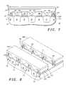
- FIG. 8is an isometric view taken in cross-section of the semiconductor component of FIG. 7 at a later stage of manufacture
- FIG. 9is a cross-sectional side view of the semiconductor component of FIG. 4 at a later stage of manufacture in accordance with another embodiment of the present invention.
- FIG. 10is a cross-sectional side view of the semiconductor component of FIG. 9 at a later stage of manufacture
- FIG. 11is a cross-sectional side view of the semiconductor component of FIG. 10 at a later stage of manufacture
- FIG. 12is a cross-sectional side view of the semiconductor component of FIG. 11 at a later stage of manufacture
- FIG. 13is a cross-sectional side view of the semiconductor component of FIG. 12 at a later stage of manufacture.
- FIG. 14is an isometric view taken in cross-section of the semiconductor component of FIG. 13 at a later stage of manufacture.
- the present inventionprovides a method for manufacturing a memory device that isolates the charge trapping structure in a memory cell or device having, for example, a SONOS type architecture.
- the charge trapping structureis also referred to as a data retention structure.
- a gap-filling materialis formed between memory cells to inhibit charge coupling between them.
- the gap-filling materialmay be formed either before or after removing a hardmask that defines the gate structure.
- the gap-filling materialimproves reliability and performance of the memory devices by maintaining the charge that has been stored in the charge storage region and inhibiting charge movement into the charge storage region during programming. It should be noted that the present invention may be used for memory devices having SONOS type architectures including NAND and NOR type configurations.
- ROMsread only memories
- PROMsprogrammable read only memories
- EPROMserasable programmable read only memories
- EEPROMselectrically erasable programmable read only memories
- FIG. 1is a cross-sectional side view of a portion of a semiconductor component 10 during manufacture in accordance with an embodiment of the present invention.
- a substrate 12having a major surface 14 and a plurality of Shallow Trench Isolation (“STI”) structures 16 formed therein.
- STIShallow Trench Isolation
- Regions 18 that are between STI structures 16are active regions, i.e., regions where the transistor action occurs.
- Suitable materials for substrate 12include silicon, polysilicon, germanium, silicon germanium, Semiconductor-On-Insulator (“SOI”) material, and the like.
- SOISemiconductor-On-Insulator
- substrate 12can be comprised of a compound semiconductor material such as Group III-V semiconductor materials, Group II-VI semiconductor materials, etc.
- the conductivity type of substrate 12is not a limitation of the present invention. In accordance with this embodiment, the conductivity type is chosen to form an N-channel insulated gate field effect transistor or semiconductor device. However, the conductivity type can be selected to form a P-channel insulated gate semiconductor device or a complementary insulated gate semiconductor device, e.g., a Complementary Metal Oxide Semiconductor (“CMOS”) device.
- CMOSComplementary Metal Oxide Semiconductor
- a charge trapping structure 20is formed on active regions 18 and STI structures 16 .
- charge trapping structure 20comprises three dielectric layers 20 A, 20 B, and 20 C having a total thickness ranging from approximately 60 Angstroms ( ⁇ ) to approximately 450 ⁇ , wherein dielectric layer 20 A is disposed on active regions 18 and STI structures 16 , dielectric layer 20 B is disposed on dielectric layer 20 A, and dielectric layer 20 C is disposed on dielectric layer 20 B.
- dielectric layer 20 Ais silicon dioxide having a thickness ranging from approximately 20 ⁇ to approximately 150 ⁇
- dielectric layer 20 Bis silicon nitride having a thickness ranging from approximately 20 ⁇ to approximately 150 ⁇
- dielectric layer 20 Cis silicon dioxide having a thickness ranging from approximately 20 ⁇ to approximately 150 ⁇ .
- charge trappingoccurs in silicon nitride layer 20 B.
- dielectric layers 20 A and 20 Chave a thickness ranging from approximately 50 ⁇ to approximately 150 ⁇ and dielectric layer 20 B has a thickness ranging from approximately 20 ⁇ to approximately 80 ⁇ .
- dielectric layers 20 A and 20 Cmay be silicon dioxide layers that are silicon-rich silicon dioxide layers; one or both of dielectric layers 20 A and 20 C may be silicon dioxide layers that are oxygen-rich silicon dioxide layers; one or both of dielectric layers 20 A and 20 C may be thermally grown or deposited oxide layers; and one or both of dielectric layers 20 A and 20 C may be silicon dioxide layers that are nitrided oxide layers.
- Dielectric layer 20 Bmay be a silicon-rich silicon nitride layer or a nitrogen-rich silicon nitride layer.
- charge trapping structure 20is not limited to being a three layer structure or a structure limited to silicon dioxide and silicon nitride.
- Charge trapping structure 20may be any dielectric layer or layers capable of trapping charge or that facilitate charge trapping.
- Other suitable materials for charge trapping structure 20include an oxide/nitride bilayer dielectric, a nitride/oxide bilayer dielectric, an oxide/tantalum oxide bilayer dielectric (SiO 2 /Ta 2 O 5 ), an oxide/tantalum oxide/oxide trilayer dielectric (SiO 2 /Ta 2 O 5 /SiO 2 ), an oxide/strontium titanate bilayer dielectric (SiO 2 /SrTiO 3 ), an oxide/barium strontium titanate bilayer dielectric (SiO 2 /BaSrTiO 2 ), an oxide/strontium titanate/oxide trilayer dielectric, an oxide/strontium titanate/oxide trilayer dielectric (SiO 2
- a layer of semiconductor material 22 having a thickness ranging from approximately 300 ⁇ to approximately 15,000 ⁇is deposited over charge trapping structure 20 .
- semiconductor layer 22is polysilicon.
- Other suitable semiconductor materials for semiconductor layer 22include doped polysilicon, doped amorphous silicon, or the like.
- a layer of dielectric material 24 having a thickness ranging from approximately 300 ⁇ to approximately 10,000 ⁇is formed on polysilicon layer 22 .
- dielectric material 24is silicon nitride.
- a layer of photoresistis formed on dielectric layer 24 and patterned to form an etch mask 26 comprising masking structures 28 and openings 30 .
- Masking structures 28are above active regions 18 and openings 30 are above STI structures 16 .
- the portions of dielectric layer 24 covered by masking structures 28are protected by etch mask 26 and the portions of dielectric layer 24 exposed by openings 30 are unprotected by etch mask 26 .
- etch mask 26the portions of dielectric layer 24 unprotected by etch mask 26 are etched away using, for example, a Reactive Ion Etch (“RIE”) that stops or terminates on polysilicon layer 22 .
- RIEReactive Ion Etch
- the reactive ion etchforms a hardmask 32 comprising masking structures 34 and openings 36 that expose portions of polysilicon layer 22 .
- Masking structures 34have sidewalls 38 .
- a layer of dielectric materialis formed on hardmask 32 and the exposed portions of polysilicon layer 22 .
- the layer of dielectric materialis anisotropically etched to form spacers 40 adjacent sidewalls 38 .
- the material of spacers 40is the same material as that of masking structures 34 . Even more preferably, masking structures 34 and spacers 40 are silicon nitride.
- masking structures 34 and spacers 40protect the portions of polysilicon layer 22 , silicon dioxide layer 20 C and silicon nitride layer 20 B that are below them, whereas the portions of polysilicon layer 22 , silicon dioxide layer 20 C and silicon nitride layer 20 B that are not below masking structures 34 and spacers 40 are unprotected.
- the distance between spacers 40 within the same opening 36ranges from approximately 50 nanometers (nm) to approximately 150 nm. By way of example, the distance is approximately 70 mm.
- the portions of polysilicon layer 22 , oxide layer 20 C, and silicon nitride layer 20 B that are unprotected by masking structures 34 and spacers 40are anisotropically etched using, for example, a reactive ion etch. It should be noted that the type of etch is not a limitation of the present invention. Thus, the portions of polysilicon layer 22 , oxide layer 20 C, and silicon nitride layer 20 B that are unprotected by masking structures 34 and spacers 40 can be etched using a wet etch, a dry etch, or a combination of a wet etch and a dry etch. The anisotropic etch stops in or on silicon dioxide layer 20 A.
- the anisotropic etchforms openings 42 in polysilicon layer 22 , silicon dioxide layer 20 C, and silicon nitride layer 20 B.
- the anisotropic etchforms polysilicon fingers 46 from polysilicon layer 22 , wherein polysilicon fingers 46 have sidewalls 48 .
- the polysilicon fingersare also referred to as conductive strips, conductive fingers, or conductive structures. In accordance with an embodiment in which the distance between spacers 40 that are within the same opening 36 is approximately 70 nm, the distance between adjacent polysilicon fingers is approximately 70 nm.
- FIGS. 1-7are two dimensional views and that polysilicon fingers 46 are preferably rectangular, i.e., they extend into the plane of the paper.
- hardmask 32 and spacers 40are removed using, for example, a reactive ion etch.
- etchis not a limitation of the present invention.
- hardmask 32 and spacers 40can be etched using a wet etch, a dry etch, or a combination of a wet etch and a dry etch.
- a layer of dielectric material 54is formed on polysilicon fingers 46 and in openings 42 .
- dielectric material 54is oxide formed by the decomposition of tetraethylorthosilicate, i.e., formed using a TEOS process.
- the method of forming dielectric layer 54is not a limitation of the present invention.
- Other suitable methods for forming dielectric layer 54include a High Temperature Oxidation (HTO) process, a Rapid Thermal Oxidation (RTO) process, or the like.
- HTOHigh Temperature Oxidation
- RTORapid Thermal Oxidation
- oxide layer 54is etched using a blanket oxide etch back technique leaving a gap-filling material 56 adjacent sidewalls 48 .
- oxide layer 54can be etched using a Chemical Mechanical Planarization (“CMP”) technique.
- CMPChemical Mechanical Planarization
- polysilicon fingers 46are cleaned to remove native oxide that may have formed on them using techniques known to those skilled in the art.
- the cleanis tailored so that gap-filling material 56 is not gouged or damaged.
- a layer of polysilicon 58is formed on polysilicon fingers 46 and gap-filling material 56 .
- polysilicon layer 58has a thickness of less than about 1,500 ⁇ .
- Polysilicon layer 58is planarized using, for example, a CMP technique. Other suitable planarization techniques include electropolishing, electrochemical polishing, chemical polishing, and chemically enhanced planarization.
- Layer 58is not limited to being polysilicon.
- Other suitable materials for layer 58include amorphous silicon, silicon carbide, gallium arsenide, indium phosphide, and the like.
- anti-reflective coating 60is formed on polysilicon layer 58 .
- anti-reflective coating 60is silicon nitride having a thickness ranging from approximately 100 ⁇ to approximately 3,000 ⁇ .
- a layer of photoresist 62is formed on anti-reflective coating 60 .
- FIG. 8an isometric view of semiconductor component 10 is shown further along in processing. It should be noted that FIG. 8 is shown as an isometric view to facilitate the description of the manufacture of semiconductor component 10 .
- Photoresist layer 62is patterned on anti-reflective coating 60 to form an etch mask layer. Anti-reflective coating 60 , polysilicon layer 58 , polysilicon layer 22 , and dielectric layers 20 B and 20 C are anisotropically etched. After etching polysilicon layer 62 , the etch chemistry is modified to etch polysilicon fingers 46 to form memory devices 70 , 72 , 74 , 76 , 78 , 80 , 82 , and 84 .
- etch mask layer and the anti-reflective coatingare removed.
- the remaining portions 58 A and 58 B of polysilicon layer 58serve as word lines.
- wordlines 58 A and 58 Bare substantially perpendicular to polysilicon fingers 46 .
- source and drain regionsare formed in active regions 18 of substrate 12 and that additional processing is typically performed to form a metallization system including contact structures.
- a layer of dielectric material 102 having a thickness ranging from approximately 100 ⁇ to approximately 15,000 ⁇is formed on polysilicon fingers 46 and in openings 42 .
- dielectric material 102is oxide formed by the decomposition of tetraethylorthosilicate, i.e., formed using a TEOS process.
- the method of forming dielectric layer 102is not a limitation of the present invention.
- Other suitable methods for forming dielectric layer 102include a High Temperature Oxidation (HTO) process, a Rapid Thermal Oxidation (RTO) process, or the like.
- oxide layer 102is etched using a blanket oxide etch back technique to form oxide plugs 104 from oxide layer 102 that are between or adjacent corresponding sidewalls 48 .
- Oxide plugs 104serve as a gap-filling material.
- oxide layer 102can be etched using a CMP technique.
- masking structures 34are removed using a wet etch such as, for example, a wet hydrofluoric acid (HF) etch or a wet phosphoric acid (H 3 PO 4 ) etch. Removing masking structures 34 leaves portions of oxide plugs 104 extending above polysilicon fingers 46 .
- a wet etchsuch as, for example, a wet hydrofluoric acid (HF) etch or a wet phosphoric acid (H 3 PO 4 ) etch.
- oxide plugs 104are planarized such that they are substantially co-planar with polysilicon fingers 46 .
- polysilicon fingers 46are cleaned to remove native oxide that may have formed on them using techniques known to those skilled in the art.
- the cleanis tailored so that oxide plugs 104 are not gouged or damaged.
- a layer of polysilicon 106is formed on polysilicon fingers 46 and oxide plugs 104 .
- polysilicon layer 106has a thickness of less than about 1,500 ⁇ .
- Polysilicon layer 106is planarized using, for example, a CMP technique. Other suitable planarization techniques include electropolishing, electrochemical polishing, chemical polishing, and chemically enhanced planarization.
- Layer 106is not limited to being polysilicon.
- Other suitable materials for layer 106include amorphous silicon, silicon carbide, gallium arsenide, indium phosphide, and the like.
- anti-reflective coating 108is formed on polysilicon layer 106 .
- anti-reflective coating 108is silicon nitride having a thickness ranging from approximately 100 ⁇ to approximately 3,000 ⁇ .
- a layer of photoresist 10is formed on anti-reflective coating 108 .
- FIG. 14an isometric view of semiconductor component 100 is shown further along in processing. It should be noted that FIG. 14 is shown as an isometric view to facilitate the description of the manufacture of semiconductor component 100 .
- Photoresist layer 110is patterned on anti-reflective coating 108 to form an etch mask layer.
- Anti-reflective coating 108 , polysilicon layer 106 , polysilicon layer 22 , and dielectric layers 20 B and 20 Care anisotropically etched. After etching polysilicon layer 106 , the etch chemistry is modified to etch polysilicon fingers 46 .
- etch chemistryis changed to form floating gate memory devices 120 , 122 , 124 , 126 , 128 , 130 , 132 , and 134 .
- the etch mask layer and the anti-reflective coatingare removed.
- the remaining portions 106 A and 106 B of polysilicon layer 106serve as word lines.
- wordlines 106 A and 106 Bare substantially perpendicular to polysilicon fingers 46 .
- source and drain regionsare formed in active regions 18 of substrate 12 and that additional processing is typically performed to form a metallization system including contact structures.
- An advantage of the present inventionis that it maintains the integrity of the charge stored in the charge storage region and therefore improves data retention.
- Another advantageis that the process flow for manufacturing the memory devices in accordance with the present invention can be integrated into a variety of process flows in a cost efficient manner.
Landscapes
- Semiconductor Memories (AREA)
- Non-Volatile Memory (AREA)
Abstract
Description
- The present invention relates, in general, to semiconductor components and, more particularly, to semiconductor memory devices.
- Semiconductor component manufacturers typically make a plurality of semiconductor components from a single semiconductor wafer. The number of integrated circuits that can be manufactured from the single semiconductor wafer ranges from one up to hundreds of thousands. Because integrated circuits are comprised of transistors or semiconductor devices, one technique for lowering the cost of manufacturing an integrated circuit is to shrink the sizes of the transistors making up the integrated circuits. In addition to lowering costs, shrinking the device sizes increases their operating speeds.
- Although the smaller transistors are capable of operating at increased speeds, other performance parameters may be degraded. For example, dual bit memory devices use a silicon-oxide-nitride-oxide-silicon (SONOS) type architecture in which a lower layer of silicon oxide is formed over a semiconductor substrate that is typically silicon. A layer of silicon nitride is formed on the lower layer of silicon oxide, an upper layer of silicon oxide is formed on the layer of silicon nitride and a layer of an electrically conductive material is formed on the upper layer of silicon oxide. The combination of the lower silicon oxide layer, the silicon nitride layer, and the upper silicon oxide layer are capable of trapping charge and are commonly referred to as a charge trapping dielectric structure or layer. When more than one bit of information is stored in the charge trapping structure, the memory device is referred to as a dual bit memory device. Bitlines are typically formed in the portion of the semiconductor substrate that is below the charge trapping structure and wordlines may be formed from the layer of electrically conductive material that is disposed on the charge trapping structure. In a dual bit memory device, two bits are stored per cell by biasing the bitline, the wordline, the source, and the drain of the memory cell such that a bit and a complementary bit are stored.
- In shrinking this type of memory device, the bitlines may be formed closer together which shortens the lengths of the channels between adjacent bitlines. As the channel lengths are decreased, isolating the charge or bits stored in the charge trapping structure becomes increasingly difficult. For example, when programming the non-complementary bit, the complementary bit may become sufficiently charged to make it difficult to distinguish between the two bits during a read operation of the non-complementary bit. In addition, shrinking the memory devices may cause short channel effects and increase leakage currents.
- Accordingly, what is needed is a memory device and a method for manufacturing the memory device that improves data retention and allows reducing the features sizes of a semiconductor device while mitigating adverse effects such as short channel effects.
- The present invention satisfies the foregoing need by providing a method for manufacturing a memory device that includes providing a semiconductor material having an active region and an isolation region. A charge trapping structure is formed over the active region and a first layer of semiconductor material is formed over the charge trapping structure. At least one masking structure having first and second sides is formed over the first layer of semiconductor material, wherein the at least one masking structure has first and second sides. At least one conductive strip having first and second sides is formed from the first layer of semiconductor material. A dielectric material is formed adjacent the first and second sides of the at least one conductive strip. A second layer of semiconductor material is formed over the at least one conductive strip and the dielectric material adjacent the first and second sides of the at least one conductive strip.
- In accordance with another embodiment, the present invention comprises a method for manufacturing a memory device that includes forming a plurality of isolation structures in a semiconductor substrate such that a first active region of the semiconductor substrate is between first and second isolation structures of the plurality of isolation structures. A data retention structure is formed over at least the first active region. A first layer of semiconductor material is formed on the data retention structure. A hardmask is formed on the first layer of semiconductor material. The hardmask protects at least one portion of the first layer of semiconductor material and leaves at least one portion of the first layer of semiconductor material unprotected. The portions of the first layer of semiconductor material and the data retention structure that are unprotected by the hardmask are etched to expose a portion of the data retention structure and to form at least one conductive strip having first and second sides. A layer of dielectric material is formed over the at least one conductive strip and the exposed portion of the data retention structure. A second layer of semiconductor material is formed over the at least one conductive strip.
- The present invention will be better understood from a reading of the following detailed description, taken in conjunction with the accompanying drawing figures in which like reference characters designate like elements and in which:
FIG. 1 is a cross-sectional side view of a semiconductor component at a beginning stage of manufacture in accordance with an embodiment of the present invention;FIG. 2 is a cross-sectional side view of the semiconductor component ofFIG. 1 at a later stage of manufacture;FIG. 3 is a cross-sectional side view of the semiconductor component ofFIG. 2 at a later stage of manufacture;FIG. 4 is a cross-sectional side view of the semiconductor component ofFIG. 3 at a later stage of manufacture;FIG. 5 is a cross-sectional side view of the semiconductor component ofFIG. 4 at a later stage of manufacture;FIG. 6 is a cross-sectional side view of the semiconductor component ofFIG. 5 at a later stage of manufacture;FIG. 7 is a cross-sectional side view of the semiconductor component ofFIG. 6 at a later stage of manufacture;FIG. 8 is an isometric view taken in cross-section of the semiconductor component ofFIG. 7 at a later stage of manufacture;FIG. 9 is a cross-sectional side view of the semiconductor component ofFIG. 4 at a later stage of manufacture in accordance with another embodiment of the present invention;FIG. 10 is a cross-sectional side view of the semiconductor component ofFIG. 9 at a later stage of manufacture;FIG. 11 is a cross-sectional side view of the semiconductor component ofFIG. 10 at a later stage of manufacture;FIG. 12 is a cross-sectional side view of the semiconductor component ofFIG. 11 at a later stage of manufacture;FIG. 13 is a cross-sectional side view of the semiconductor component ofFIG. 12 at a later stage of manufacture; andFIG. 14 is an isometric view taken in cross-section of the semiconductor component ofFIG. 13 at a later stage of manufacture.- Generally, the present invention provides a method for manufacturing a memory device that isolates the charge trapping structure in a memory cell or device having, for example, a SONOS type architecture. The charge trapping structure is also referred to as a data retention structure. In accordance with an embodiment of the present invention, a gap-filling material is formed between memory cells to inhibit charge coupling between them. The gap-filling material may be formed either before or after removing a hardmask that defines the gate structure. The gap-filling material improves reliability and performance of the memory devices by maintaining the charge that has been stored in the charge storage region and inhibiting charge movement into the charge storage region during programming. It should be noted that the present invention may be used for memory devices having SONOS type architectures including NAND and NOR type configurations. In addition, the present invention is suitable for use with read only memories (ROMs), programmable read only memories (PROMs), erasable programmable read only memories (EPROMs), electrically erasable programmable read only memories (EEPROMs), or the like.
FIG. 1 is a cross-sectional side view of a portion of asemiconductor component 10 during manufacture in accordance with an embodiment of the present invention. What is shown inFIG. 1 is asubstrate 12 having amajor surface 14 and a plurality of Shallow Trench Isolation (“STI”)structures 16 formed therein. Techniques for formingSTI structures 16 are known to those skilled in the art.Regions 18 that are betweenSTI structures 16 are active regions, i.e., regions where the transistor action occurs. Suitable materials forsubstrate 12 include silicon, polysilicon, germanium, silicon germanium, Semiconductor-On-Insulator (“SOI”) material, and the like. In addition,substrate 12 can be comprised of a compound semiconductor material such as Group III-V semiconductor materials, Group II-VI semiconductor materials, etc. The conductivity type ofsubstrate 12 is not a limitation of the present invention. In accordance with this embodiment, the conductivity type is chosen to form an N-channel insulated gate field effect transistor or semiconductor device. However, the conductivity type can be selected to form a P-channel insulated gate semiconductor device or a complementary insulated gate semiconductor device, e.g., a Complementary Metal Oxide Semiconductor (“CMOS”) device.- A
charge trapping structure 20 is formed onactive regions 18 andSTI structures 16. In accordance with one embodiment,charge trapping structure 20 comprises threedielectric layers dielectric layer 20A is disposed onactive regions 18 andSTI structures 16,dielectric layer 20B is disposed ondielectric layer 20A, anddielectric layer 20C is disposed ondielectric layer 20B. By way of example,dielectric layer 20A is silicon dioxide having a thickness ranging from approximately 20 Å to approximately 150 Å,dielectric layer 20B is silicon nitride having a thickness ranging from approximately 20 Å to approximately 150 Å, anddielectric layer 20C is silicon dioxide having a thickness ranging from approximately 20 Å to approximately 150 Å. As those skilled in the art are aware, charge trapping occurs insilicon nitride layer 20B. In accordance with one embodiment,dielectric layers dielectric layer 20B has a thickness ranging from approximately 20 Å to approximately 80 Å. - Alternatively, one or both of
dielectric layers dielectric layers dielectric layers dielectric layers Dielectric layer 20B may be a silicon-rich silicon nitride layer or a nitrogen-rich silicon nitride layer. - It should be understood that
charge trapping structure 20 is not limited to being a three layer structure or a structure limited to silicon dioxide and silicon nitride.Charge trapping structure 20 may be any dielectric layer or layers capable of trapping charge or that facilitate charge trapping. Other suitable materials forcharge trapping structure 20 include an oxide/nitride bilayer dielectric, a nitride/oxide bilayer dielectric, an oxide/tantalum oxide bilayer dielectric (SiO2/Ta2O5), an oxide/tantalum oxide/oxide trilayer dielectric (SiO2/Ta2O5/SiO2), an oxide/strontium titanate bilayer dielectric (SiO2/SrTiO3), an oxide/barium strontium titanate bilayer dielectric (SiO2/BaSrTiO2), an oxide/strontium titanate/oxide trilayer dielectric, an oxide/strontium titanate/oxide trilayer dielectric (SiO2/SrTiO3/BaSrTiO2), an oxide/hafnium oxide/oxide trilayer dielectric, and the like. Although not shown, it should be understood that a tunnel oxide may be formed betweensemiconductor substrate 12 andcharge trapping structure 20. - Still referring to
FIG. 1 , a layer ofsemiconductor material 22 having a thickness ranging from approximately 300 Å to approximately 15,000 Å is deposited overcharge trapping structure 20. In accordance with oneembodiment semiconductor layer 22 is polysilicon. Other suitable semiconductor materials forsemiconductor layer 22 include doped polysilicon, doped amorphous silicon, or the like. A layer ofdielectric material 24 having a thickness ranging from approximately 300 Å to approximately 10,000 Å is formed onpolysilicon layer 22. Preferablydielectric material 24 is silicon nitride. A layer of photoresist is formed ondielectric layer 24 and patterned to form anetch mask 26 comprising maskingstructures 28 andopenings 30. Maskingstructures 28 are aboveactive regions 18 andopenings 30 are aboveSTI structures 16. The portions ofdielectric layer 24 covered by maskingstructures 28 are protected byetch mask 26 and the portions ofdielectric layer 24 exposed byopenings 30 are unprotected byetch mask 26. - Referring now to
FIG. 2 , the portions ofdielectric layer 24 unprotected byetch mask 26 are etched away using, for example, a Reactive Ion Etch (“RIE”) that stops or terminates onpolysilicon layer 22. The reactive ion etch forms ahardmask 32 comprising maskingstructures 34 andopenings 36 that expose portions ofpolysilicon layer 22. Maskingstructures 34 have sidewalls38. - Referring now to
FIG. 3 , a layer of dielectric material is formed onhardmask 32 and the exposed portions ofpolysilicon layer 22. The layer of dielectric material is anisotropically etched to formspacers 40adjacent sidewalls 38. Preferably, the material ofspacers 40 is the same material as that of maskingstructures 34. Even more preferably, maskingstructures 34 andspacers 40 are silicon nitride. It should be noted that maskingstructures 34 andspacers 40 protect the portions ofpolysilicon layer 22,silicon dioxide layer 20C andsilicon nitride layer 20B that are below them, whereas the portions ofpolysilicon layer 22,silicon dioxide layer 20C andsilicon nitride layer 20B that are not below maskingstructures 34 andspacers 40 are unprotected. In accordance with one embodiment, the distance betweenspacers 40 within thesame opening 36 ranges from approximately 50 nanometers (nm) to approximately 150 nm. By way of example, the distance is approximately 70 mm. - Referring now to
FIG. 4 , the portions ofpolysilicon layer 22,oxide layer 20C, andsilicon nitride layer 20B that are unprotected by maskingstructures 34 andspacers 40 are anisotropically etched using, for example, a reactive ion etch. It should be noted that the type of etch is not a limitation of the present invention. Thus, the portions ofpolysilicon layer 22,oxide layer 20C, andsilicon nitride layer 20B that are unprotected by maskingstructures 34 andspacers 40 can be etched using a wet etch, a dry etch, or a combination of a wet etch and a dry etch. The anisotropic etch stops in or onsilicon dioxide layer 20A. The anisotropic etch formsopenings 42 inpolysilicon layer 22,silicon dioxide layer 20C, andsilicon nitride layer 20B. In addition, the anisotropic etch formspolysilicon fingers 46 frompolysilicon layer 22, whereinpolysilicon fingers 46 have sidewalls48. The polysilicon fingers are also referred to as conductive strips, conductive fingers, or conductive structures. In accordance with an embodiment in which the distance betweenspacers 40 that are within thesame opening 36 is approximately 70 nm, the distance between adjacent polysilicon fingers is approximately 70 nm. It should be noted thatFIGS. 1-7 are two dimensional views and thatpolysilicon fingers 46 are preferably rectangular, i.e., they extend into the plane of the paper. - Referring now to
FIG. 5 ,hardmask 32 andspacers 40 are removed using, for example, a reactive ion etch. It should be noted that the type of etch is not a limitation of the present invention. Thus, hardmask32 andspacers 40 can be etched using a wet etch, a dry etch, or a combination of a wet etch and a dry etch. A layer ofdielectric material 54 is formed onpolysilicon fingers 46 and inopenings 42. Preferablydielectric material 54 is oxide formed by the decomposition of tetraethylorthosilicate, i.e., formed using a TEOS process. The method of formingdielectric layer 54 is not a limitation of the present invention. Other suitable methods for formingdielectric layer 54 include a High Temperature Oxidation (HTO) process, a Rapid Thermal Oxidation (RTO) process, or the like. - Referring now to
FIG. 6 ,oxide layer 54 is etched using a blanket oxide etch back technique leaving a gap-fillingmaterial 56adjacent sidewalls 48. Alternatively,oxide layer 54 can be etched using a Chemical Mechanical Planarization (“CMP”) technique. - Referring now to
FIG. 7 ,polysilicon fingers 46 are cleaned to remove native oxide that may have formed on them using techniques known to those skilled in the art. Preferably, the clean is tailored so that gap-fillingmaterial 56 is not gouged or damaged. A layer ofpolysilicon 58 is formed onpolysilicon fingers 46 and gap-fillingmaterial 56. Preferably,polysilicon layer 58 has a thickness of less than about 1,500 Å.Polysilicon layer 58 is planarized using, for example, a CMP technique. Other suitable planarization techniques include electropolishing, electrochemical polishing, chemical polishing, and chemically enhanced planarization.Layer 58 is not limited to being polysilicon. Other suitable materials forlayer 58 include amorphous silicon, silicon carbide, gallium arsenide, indium phosphide, and the like. - An
anti-reflective coating 60 is formed onpolysilicon layer 58. By way of example,anti-reflective coating 60 is silicon nitride having a thickness ranging from approximately 100 Å to approximately 3,000 Å. A layer ofphotoresist 62 is formed onanti-reflective coating 60. - Referring now to
FIG. 8 , an isometric view ofsemiconductor component 10 is shown further along in processing. It should be noted thatFIG. 8 is shown as an isometric view to facilitate the description of the manufacture ofsemiconductor component 10.Photoresist layer 62 is patterned onanti-reflective coating 60 to form an etch mask layer.Anti-reflective coating 60,polysilicon layer 58,polysilicon layer 22, anddielectric layers polysilicon layer 62, the etch chemistry is modified to etchpolysilicon fingers 46 to formmemory devices portions polysilicon layer 58 serve as word lines. Preferably,wordlines polysilicon fingers 46. - Although not shown, it should be understood that source and drain regions are formed in
active regions 18 ofsubstrate 12 and that additional processing is typically performed to form a metallization system including contact structures. - Referring now to
FIG. 9 , asemiconductor component 100 is shown at an intermediate stage of manufacture in accordance with another embodiment of the present invention. It should be noted thatFIG. 9 continues from the description ofFIG. 4 . A layer ofdielectric material 102 having a thickness ranging from approximately 100 Å to approximately 15,000 Å is formed onpolysilicon fingers 46 and inopenings 42. Preferablydielectric material 102 is oxide formed by the decomposition of tetraethylorthosilicate, i.e., formed using a TEOS process. The method of formingdielectric layer 102 is not a limitation of the present invention. Other suitable methods for formingdielectric layer 102 include a High Temperature Oxidation (HTO) process, a Rapid Thermal Oxidation (RTO) process, or the like. - Referring now to
FIG. 10 ,oxide layer 102 is etched using a blanket oxide etch back technique to form oxide plugs104 fromoxide layer 102 that are between or adjacentcorresponding sidewalls 48. Oxide plugs104 serve as a gap-filling material. Alternatively,oxide layer 102 can be etched using a CMP technique. - Referring now to
FIG. 11 , maskingstructures 34 are removed using a wet etch such as, for example, a wet hydrofluoric acid (HF) etch or a wet phosphoric acid (H3PO4) etch. Removing maskingstructures 34 leaves portions of oxide plugs104 extending abovepolysilicon fingers 46. - Referring now to
FIG. 12 , oxide plugs104 are planarized such that they are substantially co-planar withpolysilicon fingers 46. - Referring now to
FIG. 13 ,polysilicon fingers 46 are cleaned to remove native oxide that may have formed on them using techniques known to those skilled in the art. Preferably, the clean is tailored so that oxide plugs104 are not gouged or damaged. A layer ofpolysilicon 106 is formed onpolysilicon fingers 46 and oxide plugs104. Preferably,polysilicon layer 106 has a thickness of less than about 1,500 Å.Polysilicon layer 106 is planarized using, for example, a CMP technique. Other suitable planarization techniques include electropolishing, electrochemical polishing, chemical polishing, and chemically enhanced planarization.Layer 106 is not limited to being polysilicon. Other suitable materials forlayer 106 include amorphous silicon, silicon carbide, gallium arsenide, indium phosphide, and the like. - An
anti-reflective coating 108 is formed onpolysilicon layer 106. By way of example,anti-reflective coating 108 is silicon nitride having a thickness ranging from approximately 100 Å to approximately 3,000 Å. A layer ofphotoresist 10 is formed onanti-reflective coating 108. - Referring now to
FIG. 14 , an isometric view ofsemiconductor component 100 is shown further along in processing. It should be noted thatFIG. 14 is shown as an isometric view to facilitate the description of the manufacture ofsemiconductor component 100.Photoresist layer 110 is patterned onanti-reflective coating 108 to form an etch mask layer.Anti-reflective coating 108,polysilicon layer 106,polysilicon layer 22, anddielectric layers polysilicon layer 106, the etch chemistry is modified to etchpolysilicon fingers 46. Then the etch chemistry is changed to form floatinggate memory devices portions polysilicon layer 106 serve as word lines. Preferably,wordlines polysilicon fingers 46. - Although not shown, it should be understood that source and drain regions are formed in
active regions 18 ofsubstrate 12 and that additional processing is typically performed to form a metallization system including contact structures. - By now it should be appreciated that memory device and a method for manufacturing the memory device have been provided. An advantage of the present invention is that it maintains the integrity of the charge stored in the charge storage region and therefore improves data retention. Another advantage is that the process flow for manufacturing the memory devices in accordance with the present invention can be integrated into a variety of process flows in a cost efficient manner.
- Although certain preferred embodiments and methods have been disclosed herein, it will be apparent from the foregoing disclosure to those skilled in the art that variations and modifications of such embodiments and methods may be made without departing from the spirit and scope of the invention. For example, the semiconductor devices can be electrically isolated from each other using LOCOS isolation structures rather than STI structures. It is intended that the invention shall be limited only to the extent required by the appended claims and the rules and principles of applicable law.
Claims (20)
Priority Applications (1)
| Application Number | Priority Date | Filing Date | Title |
|---|---|---|---|
| US11/551,535US20080096357A1 (en) | 2006-10-20 | 2006-10-20 | Method for manufacturing a memory device |
Applications Claiming Priority (1)
| Application Number | Priority Date | Filing Date | Title |
|---|---|---|---|
| US11/551,535US20080096357A1 (en) | 2006-10-20 | 2006-10-20 | Method for manufacturing a memory device |
Publications (1)
| Publication Number | Publication Date |
|---|---|
| US20080096357A1true US20080096357A1 (en) | 2008-04-24 |
Family
ID=39318442
Family Applications (1)
| Application Number | Title | Priority Date | Filing Date |
|---|---|---|---|
| US11/551,535AbandonedUS20080096357A1 (en) | 2006-10-20 | 2006-10-20 | Method for manufacturing a memory device |
Country Status (1)
| Country | Link |
|---|---|
| US (1) | US20080096357A1 (en) |
Cited By (2)
| Publication number | Priority date | Publication date | Assignee | Title |
|---|---|---|---|---|
| US20090162984A1 (en)* | 2007-12-24 | 2009-06-25 | Chung Kyung Jung | Method for manufacturing semiconductor device |
| US20140287535A1 (en)* | 2013-03-25 | 2014-09-25 | SK Hynix Inc. | Electronic device and method for fabricating the same |
Citations (24)
| Publication number | Priority date | Publication date | Assignee | Title |
|---|---|---|---|---|
| US4870470A (en)* | 1987-10-16 | 1989-09-26 | International Business Machines Corporation | Non-volatile memory cell having Si rich silicon nitride charge trapping layer |
| US5168334A (en)* | 1987-07-31 | 1992-12-01 | Texas Instruments, Incorporated | Non-volatile semiconductor memory |
| US6136647A (en)* | 1996-12-17 | 2000-10-24 | Mosel Vitelic Inc | Method of forming interpoly dielectric and gate oxide in a memory cell |
| US6223432B1 (en)* | 1999-03-17 | 2001-05-01 | Micron Technology, Inc. | Method of forming dual conductive plugs |
| US6436768B1 (en)* | 2001-06-27 | 2002-08-20 | Advanced Micro Devices, Inc. | Source drain implant during ONO formation for improved isolation of SONOS devices |
| US6440797B1 (en)* | 2001-09-28 | 2002-08-27 | Advanced Micro Devices, Inc. | Nitride barrier layer for protection of ONO structure from top oxide loss in a fabrication of SONOS flash memory |
| US6465303B1 (en)* | 2001-06-20 | 2002-10-15 | Advanced Micro Devices, Inc. | Method of manufacturing spacer etch mask for silicon-oxide-nitride-oxide-silicon (SONOS) type nonvolatile memory |
| US6570214B1 (en)* | 2002-03-01 | 2003-05-27 | Ching-Yuan Wu | Scalable stack-gate flash memory cell and its contactless memory array |
| US6630384B1 (en)* | 2001-10-05 | 2003-10-07 | Advanced Micro Devices, Inc. | Method of fabricating double densed core gates in sonos flash memory |
| US6682973B1 (en)* | 2002-05-16 | 2004-01-27 | Advanced Micro Devices, Inc. | Formation of well-controlled thin SiO, SiN, SiON layer for multilayer high-K dielectric applications |
| US20040070034A1 (en)* | 2002-10-11 | 2004-04-15 | Samsung Electronics Co., Ltd. | Semiconductor device and method of forming the same |
| US6780708B1 (en)* | 2003-03-05 | 2004-08-24 | Advanced Micro Devices, Inc. | Method of forming core and periphery gates including two critical masking steps to form a hard mask in a core region that includes a critical dimension less than achievable at a resolution limit of lithography |
| US6797565B1 (en)* | 2002-09-16 | 2004-09-28 | Advanced Micro Devices, Inc. | Methods for fabricating and planarizing dual poly scalable SONOS flash memory |
| US6828201B1 (en)* | 2001-10-22 | 2004-12-07 | Cypress Semiconductor Corporation | Method of manufacturing a top insulating layer for a sonos-type device |
| US20050048766A1 (en)* | 2003-08-31 | 2005-03-03 | Wen-Chieh Wu | Method for fabricating a conductive plug in integrated circuit |
| US6927145B1 (en)* | 2004-02-02 | 2005-08-09 | Advanced Micro Devices, Inc. | Bitline hard mask spacer flow for memory cell scaling |
| US20050176193A1 (en)* | 2004-01-15 | 2005-08-11 | Tae-Woong Kang | Method of forming a gate of a semiconductor device |
| US6933554B1 (en)* | 2000-07-11 | 2005-08-23 | Advanced Micro Devices, Inc. | Recessed tunnel oxide profile for improved reliability in NAND devices |
| US6958272B2 (en)* | 2004-01-12 | 2005-10-25 | Advanced Micro Devices, Inc. | Pocket implant for complementary bit disturb improvement and charging improvement of SONOS memory cell |
| US20050255651A1 (en)* | 2004-05-11 | 2005-11-17 | Weidong Qian | Bitline implant utilizing dual poly |
| US6969689B1 (en)* | 2002-06-28 | 2005-11-29 | Krishnaswamy Ramkumar | Method of manufacturing an oxide-nitride-oxide (ONO) dielectric for SONOS-type devices |
| US20050277250A1 (en)* | 2004-06-10 | 2005-12-15 | Macronix International Co., Ltd. | Method for fabricating a floating gate memory device |
| US20060133146A1 (en)* | 2004-12-10 | 2006-06-22 | Keiichi Maekawa | Semiconductor device and a method of manufacturing the same |
| US7119394B2 (en)* | 2004-04-22 | 2006-10-10 | Solid State System Co., Ltd. | Nonvolatile memory device and method for fabricating the same |
- 2006
- 2006-10-20USUS11/551,535patent/US20080096357A1/ennot_activeAbandoned
Patent Citations (24)
| Publication number | Priority date | Publication date | Assignee | Title |
|---|---|---|---|---|
| US5168334A (en)* | 1987-07-31 | 1992-12-01 | Texas Instruments, Incorporated | Non-volatile semiconductor memory |
| US4870470A (en)* | 1987-10-16 | 1989-09-26 | International Business Machines Corporation | Non-volatile memory cell having Si rich silicon nitride charge trapping layer |
| US6136647A (en)* | 1996-12-17 | 2000-10-24 | Mosel Vitelic Inc | Method of forming interpoly dielectric and gate oxide in a memory cell |
| US6223432B1 (en)* | 1999-03-17 | 2001-05-01 | Micron Technology, Inc. | Method of forming dual conductive plugs |
| US6933554B1 (en)* | 2000-07-11 | 2005-08-23 | Advanced Micro Devices, Inc. | Recessed tunnel oxide profile for improved reliability in NAND devices |
| US6465303B1 (en)* | 2001-06-20 | 2002-10-15 | Advanced Micro Devices, Inc. | Method of manufacturing spacer etch mask for silicon-oxide-nitride-oxide-silicon (SONOS) type nonvolatile memory |
| US6436768B1 (en)* | 2001-06-27 | 2002-08-20 | Advanced Micro Devices, Inc. | Source drain implant during ONO formation for improved isolation of SONOS devices |
| US6440797B1 (en)* | 2001-09-28 | 2002-08-27 | Advanced Micro Devices, Inc. | Nitride barrier layer for protection of ONO structure from top oxide loss in a fabrication of SONOS flash memory |
| US6630384B1 (en)* | 2001-10-05 | 2003-10-07 | Advanced Micro Devices, Inc. | Method of fabricating double densed core gates in sonos flash memory |
| US6828201B1 (en)* | 2001-10-22 | 2004-12-07 | Cypress Semiconductor Corporation | Method of manufacturing a top insulating layer for a sonos-type device |
| US6570214B1 (en)* | 2002-03-01 | 2003-05-27 | Ching-Yuan Wu | Scalable stack-gate flash memory cell and its contactless memory array |
| US6682973B1 (en)* | 2002-05-16 | 2004-01-27 | Advanced Micro Devices, Inc. | Formation of well-controlled thin SiO, SiN, SiON layer for multilayer high-K dielectric applications |
| US6969689B1 (en)* | 2002-06-28 | 2005-11-29 | Krishnaswamy Ramkumar | Method of manufacturing an oxide-nitride-oxide (ONO) dielectric for SONOS-type devices |
| US6797565B1 (en)* | 2002-09-16 | 2004-09-28 | Advanced Micro Devices, Inc. | Methods for fabricating and planarizing dual poly scalable SONOS flash memory |
| US20040070034A1 (en)* | 2002-10-11 | 2004-04-15 | Samsung Electronics Co., Ltd. | Semiconductor device and method of forming the same |
| US6780708B1 (en)* | 2003-03-05 | 2004-08-24 | Advanced Micro Devices, Inc. | Method of forming core and periphery gates including two critical masking steps to form a hard mask in a core region that includes a critical dimension less than achievable at a resolution limit of lithography |
| US20050048766A1 (en)* | 2003-08-31 | 2005-03-03 | Wen-Chieh Wu | Method for fabricating a conductive plug in integrated circuit |
| US6958272B2 (en)* | 2004-01-12 | 2005-10-25 | Advanced Micro Devices, Inc. | Pocket implant for complementary bit disturb improvement and charging improvement of SONOS memory cell |
| US20050176193A1 (en)* | 2004-01-15 | 2005-08-11 | Tae-Woong Kang | Method of forming a gate of a semiconductor device |
| US6927145B1 (en)* | 2004-02-02 | 2005-08-09 | Advanced Micro Devices, Inc. | Bitline hard mask spacer flow for memory cell scaling |
| US7119394B2 (en)* | 2004-04-22 | 2006-10-10 | Solid State System Co., Ltd. | Nonvolatile memory device and method for fabricating the same |
| US20050255651A1 (en)* | 2004-05-11 | 2005-11-17 | Weidong Qian | Bitline implant utilizing dual poly |
| US20050277250A1 (en)* | 2004-06-10 | 2005-12-15 | Macronix International Co., Ltd. | Method for fabricating a floating gate memory device |
| US20060133146A1 (en)* | 2004-12-10 | 2006-06-22 | Keiichi Maekawa | Semiconductor device and a method of manufacturing the same |
Cited By (4)
| Publication number | Priority date | Publication date | Assignee | Title |
|---|---|---|---|---|
| US20090162984A1 (en)* | 2007-12-24 | 2009-06-25 | Chung Kyung Jung | Method for manufacturing semiconductor device |
| US20140287535A1 (en)* | 2013-03-25 | 2014-09-25 | SK Hynix Inc. | Electronic device and method for fabricating the same |
| US9627616B2 (en)* | 2013-03-25 | 2017-04-18 | SK Hynix Inc. | Electronic device and method for fabricating the same |
| US9972384B2 (en) | 2013-03-25 | 2018-05-15 | SK Hynix Inc. | Electronic device and method for fabricating the same |
Similar Documents
| Publication | Publication Date | Title |
|---|---|---|
| US8106475B2 (en) | Semiconductor device and method of manufacturing the same | |
| US7033909B2 (en) | Method of forming trench isolations | |
| US7560353B2 (en) | Methods of fabricating memory devices with memory cell transistors having gate sidewall spacers with different dielectric properties | |
| US7384843B2 (en) | Method of fabricating flash memory device including control gate extensions | |
| US6972260B2 (en) | Method of fabricating flash memory cell | |
| US20020033501A1 (en) | Nonvolatile semiconductor memory and method of fabricating the same | |
| US6642568B2 (en) | Semiconductor device and method of manufacturing the same | |
| US20060175718A1 (en) | Semiconductor device and method of manufacturing the same | |
| US6436751B1 (en) | Fabrication method and structure of a flash memory | |
| US8778760B2 (en) | Method of manufacturing flash memory cell | |
| US9780107B2 (en) | Methods of forming integrated circuit devices | |
| US6531360B2 (en) | Method of manufacturing a flash memory device | |
| US8952536B2 (en) | Semiconductor device and method of fabrication | |
| US7335940B2 (en) | Flash memory and manufacturing method thereof | |
| US20080096357A1 (en) | Method for manufacturing a memory device | |
| US7172939B1 (en) | Method and structure for fabricating non volatile memory arrays | |
| US8802537B1 (en) | System and method for improving reliability in a semiconductor device | |
| US20070138538A1 (en) | Method of forming self-aligned floating gate array and flash memory device including self-aligned floating gate array | |
| KR100823694B1 (en) | Method of forming floating gate structure of nonvolatile memory device | |
| KR20060007176A (en) | Manufacturing method of nonvolatile memory device | |
| KR20070067563A (en) | How to Form a Floating Gate |
Legal Events
| Date | Code | Title | Description |
|---|---|---|---|
| AS | Assignment | Owner name:SPANSION LLC, CALIFORNIA Free format text:ASSIGNMENT OF ASSIGNORS INTEREST;ASSIGNORS:SUH, YOUSEOK, MR.;SHIRAIWA, HIDEHIKO;HOLBROOK, ALLISON;AND OTHERS;REEL/FRAME:018418/0860;SIGNING DATES FROM 20060216 TO 20060321 Owner name:ADVANCED MICRO DEVICES, INC., CALIFORNIA Free format text:ASSIGNMENT OF ASSIGNORS INTEREST;ASSIGNOR:HUI, ANGELA;REEL/FRAME:018418/0924 Effective date:20060519 | |
| AS | Assignment | Owner name:GLOBALFOUNDRIES INC., CAYMAN ISLANDS Free format text:AFFIRMATION OF PATENT ASSIGNMENT;ASSIGNOR:ADVANCED MICRO DEVICES, INC.;REEL/FRAME:023120/0426 Effective date:20090630 Owner name:GLOBALFOUNDRIES INC.,CAYMAN ISLANDS Free format text:AFFIRMATION OF PATENT ASSIGNMENT;ASSIGNOR:ADVANCED MICRO DEVICES, INC.;REEL/FRAME:023120/0426 Effective date:20090630 | |
| AS | Assignment | Owner name:BARCLAYS BANK PLC,NEW YORK Free format text:SECURITY AGREEMENT;ASSIGNORS:SPANSION LLC;SPANSION INC.;SPANSION TECHNOLOGY INC.;AND OTHERS;REEL/FRAME:024522/0338 Effective date:20100510 Owner name:BARCLAYS BANK PLC, NEW YORK Free format text:SECURITY AGREEMENT;ASSIGNORS:SPANSION LLC;SPANSION INC.;SPANSION TECHNOLOGY INC.;AND OTHERS;REEL/FRAME:024522/0338 Effective date:20100510 | |
| STCB | Information on status: application discontinuation | Free format text:ABANDONED -- AFTER EXAMINER'S ANSWER OR BOARD OF APPEALS DECISION | |
| AS | Assignment | Owner name:SPANSION TECHNOLOGY LLC, CALIFORNIA Free format text:RELEASE BY SECURED PARTY;ASSIGNOR:BARCLAYS BANK PLC;REEL/FRAME:035201/0159 Effective date:20150312 Owner name:SPANSION INC., CALIFORNIA Free format text:RELEASE BY SECURED PARTY;ASSIGNOR:BARCLAYS BANK PLC;REEL/FRAME:035201/0159 Effective date:20150312 Owner name:SPANSION LLC, CALIFORNIA Free format text:RELEASE BY SECURED PARTY;ASSIGNOR:BARCLAYS BANK PLC;REEL/FRAME:035201/0159 Effective date:20150312 | |
| AS | Assignment | Owner name:GLOBALFOUNDRIES U.S. INC., NEW YORK Free format text:RELEASE BY SECURED PARTY;ASSIGNOR:WILMINGTON TRUST, NATIONAL ASSOCIATION;REEL/FRAME:056987/0001 Effective date:20201117 |