US20080096330A1 - High-performance cmos soi devices on hybrid crystal-oriented substrates - Google Patents
High-performance cmos soi devices on hybrid crystal-oriented substratesDownload PDFInfo
- Publication number
- US20080096330A1 US20080096330A1US11/958,877US95887707AUS2008096330A1US 20080096330 A1US20080096330 A1US 20080096330A1US 95887707 AUS95887707 AUS 95887707AUS 2008096330 A1US2008096330 A1US 2008096330A1
- Authority
- US
- United States
- Prior art keywords
- semiconductor
- semiconductor layer
- bonded substrate
- layer
- semiconductor material
- Prior art date
- Legal status (The legal status is an assumption and is not a legal conclusion. Google has not performed a legal analysis and makes no representation as to the accuracy of the status listed.)
- Granted
Links
- 239000000758substrateSubstances0.000titleclaimsabstractdescription63
- 239000004065semiconductorSubstances0.000claimsabstractdescription207
- 238000000034methodMethods0.000claimsabstractdescription51
- 239000000463materialSubstances0.000claimsabstractdescription45
- 235000012431wafersNutrition0.000claimsdescription40
- 238000005530etchingMethods0.000claimsdescription31
- 239000013078crystalSubstances0.000claimsdescription23
- 150000004767nitridesChemical class0.000claimsdescription23
- 238000002955isolationMethods0.000claimsdescription15
- 125000006850spacer groupChemical group0.000claimsdescription11
- 229910000577Silicon-germaniumInorganic materials0.000claimsdescription9
- 229920002120photoresistant polymerPolymers0.000claimsdescription8
- 239000007943implantSubstances0.000claimsdescription7
- 238000010438heat treatmentMethods0.000claimsdescription6
- 239000012212insulatorSubstances0.000claimsdescription5
- 229910003811SiGeCInorganic materials0.000claimsdescription4
- 229910045601alloyInorganic materials0.000claimsdescription4
- 239000000956alloySubstances0.000claimsdescription4
- 229910003465moissaniteInorganic materials0.000claimsdescription4
- 229910052710siliconInorganic materials0.000claimsdescription4
- 229910010271silicon carbideInorganic materials0.000claimsdescription4
- 239000000126substanceSubstances0.000claimsdescription4
- 238000000227grindingMethods0.000claimsdescription3
- 238000005498polishingMethods0.000claimsdescription3
- 239000010410layerSubstances0.000description131
- 230000037230mobilityEffects0.000description11
- 239000004020conductorSubstances0.000description6
- 238000000151depositionMethods0.000description5
- 230000008021depositionEffects0.000description5
- 150000002500ionsChemical class0.000description5
- 238000009792diffusion processMethods0.000description4
- 238000001020plasma etchingMethods0.000description4
- 230000015572biosynthetic processEffects0.000description3
- 238000005229chemical vapour depositionMethods0.000description3
- 238000005137deposition processMethods0.000description3
- 238000001459lithographyMethods0.000description3
- 230000003647oxidationEffects0.000description3
- 238000007254oxidation reactionMethods0.000description3
- 239000010703siliconSubstances0.000description3
- 229910001218Gallium arsenideInorganic materials0.000description2
- 229910000927Ge alloyInorganic materials0.000description2
- 229910000673Indium arsenideInorganic materials0.000description2
- 230000000295complement effectEffects0.000description2
- 150000001875compoundsChemical class0.000description2
- 230000001419dependent effectEffects0.000description2
- 238000011049fillingMethods0.000description2
- RPQDHPTXJYYUPQ-UHFFFAOYSA-Nindium arsenideChemical compound[In]#[As]RPQDHPTXJYYUPQ-UHFFFAOYSA-N0.000description2
- 239000011810insulating materialSubstances0.000description2
- 230000000873masking effectEffects0.000description2
- 229910044991metal oxideInorganic materials0.000description2
- 150000004706metal oxidesChemical class0.000description2
- 238000000231atomic layer depositionMethods0.000description1
- 230000004888barrier functionEffects0.000description1
- 230000015556catabolic processEffects0.000description1
- 238000000224chemical solution depositionMethods0.000description1
- 238000006731degradation reactionMethods0.000description1
- 238000000280densificationMethods0.000description1
- 238000001312dry etchingMethods0.000description1
- 239000011261inert gasSubstances0.000description1
- 238000005468ion implantationMethods0.000description1
- 238000010884ion-beam techniqueMethods0.000description1
- 238000010329laser etchingMethods0.000description1
- 239000000203mixtureSubstances0.000description1
- 238000000059patterningMethods0.000description1
- 238000000623plasma-assisted chemical vapour depositionMethods0.000description1
- 230000005855radiationEffects0.000description1
- 239000002344surface layerSubstances0.000description1
- 238000001039wet etchingMethods0.000description1
Images


Classifications
- H—ELECTRICITY
- H01—ELECTRIC ELEMENTS
- H01L—SEMICONDUCTOR DEVICES NOT COVERED BY CLASS H10
- H01L21/00—Processes or apparatus adapted for the manufacture or treatment of semiconductor or solid state devices or of parts thereof
- H01L21/70—Manufacture or treatment of devices consisting of a plurality of solid state components formed in or on a common substrate or of parts thereof; Manufacture of integrated circuit devices or of parts thereof
- H01L21/71—Manufacture of specific parts of devices defined in group H01L21/70
- H01L21/76—Making of isolation regions between components
- H01L21/762—Dielectric regions, e.g. EPIC dielectric isolation, LOCOS; Trench refilling techniques, SOI technology, use of channel stoppers
- H01L21/7624—Dielectric regions, e.g. EPIC dielectric isolation, LOCOS; Trench refilling techniques, SOI technology, use of channel stoppers using semiconductor on insulator [SOI] technology
- H01L21/76264—SOI together with lateral isolation, e.g. using local oxidation of silicon, or dielectric or polycristalline material refilled trench or air gap isolation regions, e.g. completely isolated semiconductor islands
- H01L21/76275—Vertical isolation by bonding techniques
- H—ELECTRICITY
- H10—SEMICONDUCTOR DEVICES; ELECTRIC SOLID-STATE DEVICES NOT OTHERWISE PROVIDED FOR
- H10D—INORGANIC ELECTRIC SEMICONDUCTOR DEVICES
- H10D84/00—Integrated devices formed in or on semiconductor substrates that comprise only semiconducting layers, e.g. on Si wafers or on GaAs-on-Si wafers
- H10D84/01—Manufacture or treatment
- H10D84/0123—Integrating together multiple components covered by H10D12/00 or H10D30/00, e.g. integrating multiple IGBTs
- H10D84/0126—Integrating together multiple components covered by H10D12/00 or H10D30/00, e.g. integrating multiple IGBTs the components including insulated gates, e.g. IGFETs
- H10D84/0165—Integrating together multiple components covered by H10D12/00 or H10D30/00, e.g. integrating multiple IGBTs the components including insulated gates, e.g. IGFETs the components including complementary IGFETs, e.g. CMOS devices
- H10D84/0167—Manufacturing their channels
- H—ELECTRICITY
- H10—SEMICONDUCTOR DEVICES; ELECTRIC SOLID-STATE DEVICES NOT OTHERWISE PROVIDED FOR
- H10D—INORGANIC ELECTRIC SEMICONDUCTOR DEVICES
- H10D84/00—Integrated devices formed in or on semiconductor substrates that comprise only semiconducting layers, e.g. on Si wafers or on GaAs-on-Si wafers
- H10D84/01—Manufacture or treatment
- H10D84/02—Manufacture or treatment characterised by using material-based technologies
- H10D84/03—Manufacture or treatment characterised by using material-based technologies using Group IV technology, e.g. silicon technology or silicon-carbide [SiC] technology
- H10D84/038—Manufacture or treatment characterised by using material-based technologies using Group IV technology, e.g. silicon technology or silicon-carbide [SiC] technology using silicon technology, e.g. SiGe
- H—ELECTRICITY
- H10—SEMICONDUCTOR DEVICES; ELECTRIC SOLID-STATE DEVICES NOT OTHERWISE PROVIDED FOR
- H10D—INORGANIC ELECTRIC SEMICONDUCTOR DEVICES
- H10D86/00—Integrated devices formed in or on insulating or conducting substrates, e.g. formed in silicon-on-insulator [SOI] substrates or on stainless steel or glass substrates
- H10D86/01—Manufacture or treatment
Definitions
- the present inventionrelates to semiconductor devices, and more particularly to integrated semiconductor devices, such as silicon-on-insulator (SOI)/complementary metal oxide semiconductor (CMOS) devices, that are formed on a hybrid crystal oriented substrate.
- the present inventionprovides a means for integrating at least two types of semiconductor devices, such as NFETs and PFETs, onto a bonded substrate having different crystallographic orientations. The location of each device on the bonded substrate is dependent upon the performance of that device has on a particular crystal orientation.
- the present inventionforms NFETs on a (100) surface, while the PFETs are formed on a (110) surface.
- the (100) crystal surfaceprovides NFETs with high performance, while the (110) crystal surface provides PFETs with high performance.
- CMOS devicessuch as NFETs or PFETs
- semiconductor waferssuch as Si
- Sisemiconductor wafers
- most of today's semiconductor devicesare built upon Si having a (100) crystal orientation.
- Electronsare known to have a high mobility for a (100) Si surface orientation, but holes are known to have high mobility for a (110) surface orientation. That is, hole mobility values on (100) Si are roughly 2 ⁇ -4 ⁇ lower than the corresponding electron hole mobility for this crystallographic orientation.
- PFETsare typically designed with larger widths in order to balance pull-up currents against the NFET pull-down currents and achieve uniform circuit switching. NFETs having larger widths are undesirable since they take up a significant amount of chip area.
- the (110) Si surfaceis optimal for PFET devices because of excellent hole mobility, yet such a crystal orientation is completely inappropriate for NFET devices. Instead, the (100) Si surface is optimal for NFET devices since that crystal orientation favors electron mobility.
- One object of the present inventionis to provide a method of integrating semiconductor devices such that different types of devices are formed upon a specific crystal orientation of a bonded substrate that enhances the performance of the device.
- Another object of the present inventionis to provide a method of integrating semiconductor devices such that the PFETs are located on a (110) crystallographic plane, while the NFETs are located on a (100) crystallographic plane of a bonded substrate.
- a further object of the present inventionis to provide a method of integrating silicon-on-insulator (SOI) technology with complementary metal oxide semiconductor (CMOS) technology using simple and easy processing steps.
- SOIsilicon-on-insulator
- CMOScomplementary metal oxide semiconductor
- a still further object of the present inventionis to provide a method in which one CMOS device will be SOI-like, while the other CMOS device will be bulk-like.
- An even further object of the present inventionis to provide a method in which both CMOS devices being integrated are SOI-like.
- a yet even further object of the present inventionis to provide a method to integrate strained-silicon NFETs on a (100) crystallographic surface plane with silicon or strained-silicon PFETs on a (110) crystallographic surface plane.
- An additional object of the present inventionis to provide a method of integrating different CMOS devices onto a bonded substrate having different crystallographic surface planes wherein isolation regions are formed between the different types of CMOS devices.
- the method of the present inventioncomprises the steps of:
- a bonded substratecomprising at least a first semiconductor layer of a first crystallographic orientation and a second semiconductor layer of a second crystallographic orientation separated by an insulating layer, said first
- crystallographic orientationis different from said second crystallographic orientation and said first semiconductor layer lies above said second semiconductor layer;
- the first semiconductor devicemay be a PFET and the first crystallographic orientation may be (110) or (111), while the second semiconductor device may be an NFET and the second crystallographic orientation may be (100) or (111). It is also possible in the present invention, that the first semiconductor device is a NFET and that the second semiconductor device is a PFET.
- the methodfurther includes forming isolation regions between the first device region and the second device region.
- the semiconductor materialcomprises an upper layer of strained Si and a lower layer of relaxed SiGe alloy or a SiC alloy.
- Another aspect of the present inventionrelates to an integrated semiconductor structure containing at least two types of devices, wherein at least one of the devices is formed upon a first crystallographic surface that is optimal for that device, while the other device is formed upon a second crystallographic surface, which is different from the first, that is optimal for the other device.
- the structure of the present inventioncomprises:
- a bonded substratecomprising a first device region having a first crystallographic orientation and a second device region having a second crystallographic orientation, said first crystallographic orientation is different from said second crystallographic orientation;
- At least one first semiconductor device located in said first device region and at least one second semiconductor device located in said second device regionare at least one first semiconductor device located in said first device region and at least one second semiconductor device located in said second device region.
- the first semiconductor devicemay be a PFET and the first crystallographic orientation may be (110) or (111), while the second semiconductor device may be an NFET and the second crystallographic orientation may be (100) or (111). It is also possible in the present invention that the first semiconductor device is an NFET and the second semiconductor device is a PFET.
- the configuration of the semiconductor deviceswill be dependent on the crystal orientation of the bonded substrate.
- FIGS. 2A-2Fare pictorial representations (through cross sectional views) illustrating the basic processing steps utilized in the present invention in forming integrated CMOS devices on different crystallographic orientation planes of a bonded substrate.
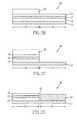
- FIGS. 3A-3Dare pictorial representations of various wafers that may be bonded together and used in the method described in FIGS. 2A-2E .
- FIGS. 4A-4Jare pictorial representations (through cross sectional views) illustrating the basic processing steps used in forming a high performance semiconductor device containing two NFETs formed on a (100) crystallographic surface, and a PFET, which is located between the NFETs, formed on a (110) crystallographic surface.
- FIGS. 5A-5Gare pictorial representations (through cross sectional views) illustrating alternative processing steps used in forming a high performance semiconductor device containing two NFETs formed on a (100) crystallographic surface, and a PFET, which is located between the NFETs, formed on a (110) crystallographic surface.
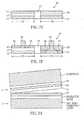
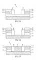
- FIG. 2Aillustrate a bonded substrate 10 , i.e., hybrid substrate, which may be employed in the present invention.
- bonded substrate 10includes a surface dielectric layer 18 , a first semiconductor layer 16 , an insulating layer 14 , and a second semiconductor layer 12 .
- the bonded substrate 10may further include an optional third semiconductor layer (not shown) that is located beneath the second semiconductor layer 12 .
- another insulating layerseparates the second semiconductor layer 12 from the optional third semiconductor layer.
- the surface dielectric layer 18 of the bonded substrate 10is an oxide, nitride, oxynitride or other insulating layer that is either present in one of the initial wafers before bonding, or formed atop the first semiconductor layer 16 after wafer bonding by either a thermal process (i.e., oxidation, nitridation or oxynitridation) or by deposition. Notwithstanding the origin of the surface dielectric layer 18 , the surface dielectric layer 18 has a thickness of from about 3 to about 500 nm, with a thickness of from about 5 to about 20 nm being more highly preferred.
- the first semiconductor layer 16is comprised of any semiconducting material including, for example, Si, SiC, SiGe, SiGeC, Ge alloys, GaAs, InAs, InP as well as other III/V or II/VI compound semiconductors.
- First semiconductor layer 16may also comprise an SOI layer of a preformed SOI substrate or a layered semiconductor such as, for example, Si/SiGe.
- the first semiconductor layer 16is also characterized as having a first crystallographic orientation, which is preferably (110). Although a (110) crystal orientation is preferred, the first semiconductor layer 16 may have a (111), or a (100) crystal orientation.
- the thickness of the first semiconductor layer 16may vary depending on the initial starting wafers used to form the bonded substrate 10 . Typically, however, the first semiconductor layer 16 has a thickness of from about 5 to about 500 nm, with a thickness of from about 5 to about 100 nm being more highly preferred.
- the insulating layer 14which is located between the first semiconductor layer 16 and the second semiconductor layer 12 has a variable thickness depending upon the initial wafers used to create the bonded substrate 10 . Typically, however, the insulating layer 14 has a thickness of from about 1 to about 5 nm, with a thickness of from about 5 to about 100 nm being more highly preferred.
- the insulating layer 14is an oxide or other like insulator material that is formed on one or both of the wafers prior to bonding.
- the second semiconductor layer 12is comprised of any semiconducting material which may be the same or different from that of the first semiconductor layer 16 .
- second semiconductor layer 12may include, for example, Si, SiC, SiGe, SiGeC, Ge alloys, GaAs, InAs, InP as well as other III/V or II/VI compound semiconductors.
- Second semiconductor layer 12may also comprise an SOI layer of a preformed SOI substrate or a layered semiconductor such as, for example, Si/SiGe.
- the second semiconductor layer 12is also characterized as having a second crystallographic orientation, which is different from the first crystallographic orientation. Since the first semiconductor layer 16 is preferably a (110) surface, the crystallographic orientation of the second semiconductor layer 12 is preferably (100). Although a (100) crystal orientation is preferred, the second semiconductor layer 12 may have a (111), or a (110) crystal structure.
- the thickness of the second semiconductor layer 12may vary depending on the initial starting wafers used to form the bonded substrate 10 . Typically, however, the second semiconductor layer 12 has a thickness of from about 5 nm to about 200 ⁇ m, with a thickness of from about 5 to about 100 nm being more highly preferred.
- the optional third semiconductor layermay comprise the same or different semiconducting material as that of the second semiconductor layer 12 .
- the crystal orientation of the optional third semiconductor layeris typically, but not always, the same as the second semiconductor layer.
- the optional third semiconductor layeris generally thicker than the second semiconductor layer 12 .
- an insulating layerseparates the optional third semiconductor layer from the second semiconductor layer.
- the bonded substrate 10 illustrated in FIG. 2Ais comprised of two semiconductor wafers that are bonded together.
- the two wafers used in fabricating the bonded substrate 10may include two SOI wafers (See, FIG. 3A ), wherein one of the wafers, designated as 1 , includes the first semiconductor layer 16 and the other wafer, designated as 2 includes the second semiconductor 12 ; an SOI wafer (designated as 2 ) and a bulk semiconductor wafer (designated as 1 ; see, FIG. 3B ); two bulk semiconductor wafers (designated as 1 and 2 , respectively; see FIG.
- Bondingis achieved by first bringing the two wafers into intimate contact with other; optionally applying an external force to the contacted wafers; and then heating the two contacted wafers under conditions that are capable of bonding the two wafers together.
- the heating stepmay be performed in the presence or absence of an external force.
- the heating stepis typically performed in an inert ambient at a temperature of from about 200° to about 1050° C. for a time period of from about 2 to about 20 hours. More preferably, the bonding is performed at a temperature of from about 200° to about 400° C. for a time period of from about 2 to about 20 hours.
- inert ambientis used in the present invention to denote an atmosphere in which an inert gas, such as He, Ar, N 2 , Xe, Kr or a mixture thereof, is employed.
- a preferred ambient used during the bonding processis N 2 .
- some material layers of at least one of the SOI wafersmay be removed after bonding utilizing a planarization process such as chemical mechanical polishing (CMP) or grinding and etching.
- CMPchemical mechanical polishing
- the planarization processstops when surface dielectric layer 18 is reached.
- the ion implant regionforms a porous region during bonding which causes a portion of the wafer above the ion implant region to break off leaving a bonded wafer such as is shown, for example, in FIG. 1A .
- the implant regionis typically comprised of H 2 ions which are implanted into the surface of the wafer utilizing ion implantation conditions that are well known to those skilled in the art.
- the surface dielectric layer 18may be formed atop the bonded wafers by a thermal process, such as oxidation, or by a conventional deposition process such as chemical vapor deposition (CVD), plasma-enhanced CVD, atomic layer deposition, chemical solution deposition as well as other like deposition processes.
- CVDchemical vapor deposition
- atomic layer depositionatomic layer deposition
- chemical solution depositionchemical solution deposition as well as other like deposition processes.
- Mask 20is then formed on a predetermined portion of the bonded substrate 10 of FIG. 2A so as to protect a portion of the bonded substrate 10 , while leaving another portion of the bonded substrate 10 unprotected.
- the protected portion of the bonded substrate 10defines a first device region 22 of the structure, whereas the unprotected portion of the bonded substrate 10 defines a second device area 24 .
- mask 20is formed on a predetermined portion of the surface dielectric layer 18 by applying a photoresist mask to the entire surface of the bonded substrate 10 . After application of the photoresist mask, the mask is patterned by lithography, which includes the steps of exposing the photoresist to a pattern of radiation and developing the pattern utilizing a resist developer.
- the resultant structure including the mask 20 formed on a predetermined portion of the bonded substrate 10is shown, for example, in FIG. 2B .
- mask 20is a nitride or oxynitride layer that is formed and patterned utilizing lithography and etching. The nitride or oxynitride mask 20 may be removed after defining the region for the second semiconductor device.
- the structureis subjected to one or more etching steps so as to expose a surface of the second semiconductor layer 12 .
- the one or more etching steps used at this point of the present inventionremoves the unprotected portions of the surface dielectric layer 18 , as well as underlying portions of the first semiconductor layer 16 , and a portion of the insulating layer 14 which separated the first semiconductor layer 16 from the second semiconductor layer 12 .
- the etchingmay be performed utilizing a single etching process or multiple etching steps may be employed.
- the etching used at this point of the present inventionmay include a dry etching process such as reactive-ion etching, ion beam etching, plasma etching or laser etching, a wet etching process wherein a chemical etchant is employed or any combination thereof.
- RIEreactive-ion etching
- the sidewalls of the protected first device region 22i.e., the surface dielectric layer 18 , the first semiconductor layer 16 , the insulating layer 14 and the second semiconductor layer 12 , are exposed after this etching step. As shown, the exposed sidewalls of layers 18 , 16 and 14 are aligned with an outer most edge of mask 20 .
- the mask 20is then removed from the structure shown in FIG. 2C utilizing a conventional resist stripping process and then a liner or spacer 25 is formed on the exposed sidewalls.
- the liner or spacer 25is formed by deposition and etching.
- the liner or spacer 25is comprised of an insulating material such as, for example, an oxide.
- a semiconductor material 26is formed on the exposed second semiconductor layer 12 .
- semiconductor material 26has a crystallographic orientation that is the same as the crystallographic orientation of the second semiconductor layer 12 .
- the resultant structureis shown, for example, in FIG. 2D .
- the semiconductor material 26may comprise any Si-containing semiconductor, such as Si, strained Si, SiGe, SiC, SiGeC or combinations thereof which is capable of being formed utilizing a selective epitaxial growth method.
- semiconductor material 26is comprised of Si.
- the semiconductor materialis a strained Si layer that is located atop a relaxed SiGe alloy layer.
- semiconductor material 26may be referred to as a regrown semiconductor material.
- the structure shown in FIG. 2Dis subjected to a planarization process such as chemical mechanical polishing (CMP) or grinding such that the upper surface of the semiconductor material 26 is substantially planar with the upper surface of the first semiconductor layer 16 . Note that previously protected portion of surface dielectric layer 18 is removed during this planarization process.
- CMPchemical mechanical polishing
- an isolation region 27such as a shallow trench isolation region, is typically formed so as to isolate the first semiconductor device region 22 from the second semiconductor device region 24 .
- the isolation region 27is formed utilizing processing steps that are well known to those skilled in the art including, for example, trench definition and etching; optionally lining the trench with a diffusion barrier; and filling the trench with a trench dielectric such as an oxide. After the trench fill, the structure may be planarized and an optional densification process step may be performed to density the trench dielectric.
- the resultant substantially planar structure containing isolation region 27is show, for example, in FIG. 2E .
- the structure of FIG. 2Bincludes an exposed first semiconductor layer 16 of a first crystal orientation and an unexposed regrown semiconductor material 26 that has the same crystal orientation as that of the second semiconductor layer 12 .
- FIG. 2Fshows the integrated structure that is formed after a first semiconductor device 30 is formed on a portion of the first semiconductor layer 16 and a second semiconductor device 32 is formed on the regrown semiconductor material 26 .
- the present inventioncontemplates forming a plurality of each type of device in the specific device region.
- the first semiconductor devicemay be a PFET or a NFET
- the second semiconductor devicemay be a NFET or PFET, with the proviso that the first semiconductor device is different from the second semiconductor device and that the specific device is fabricating on a crystal orientation that provides a high performance device.
- Each FETincludes a gate dielectric, a gate conductor, an optional hard mask located atop the gate conductor, spacers located on sidewalls of at least the gate conductor, and source/drain diffusion regions.
- the diffusion regionsare labeled as 34 in FIG. 2F . Note that the PFET is formed over the semiconductor material that has a (110), or (111) orientation, whereas the NFET is formed over a semiconductor surface having a (100), or (111) orientation.
- FIGS. 2A-2Fillustrate the basic concept of the present invention which includes providing a bonded substrate having two different crystallographic orientations, masking, etching, regrowth, planarization and device formation.
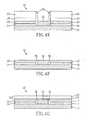
- FIGS. 4A-4Jillustrate processing steps used in forming a high performance semiconductor device containing two NFETs formed on a (100) crystallographic surface, and a PFET, which is located between the NFETs, formed on a (110) crystallographic surface.
- FIG. 4Aillustrates a bonded substrate 10 that may be used in this embodiment of the present invention.
- the bonded substrate 10includes a surface dielectric layer 18 , a first semiconductor layer 16 , an insulating layer 14 and a second semiconductor layer 12 .
- a third optional semiconductor layermay be located beneath the second semiconductor layer 12 .
- an insulating layerseparates the second semiconductor layer from the optional third semiconductor layer.
- FIG. 4Billustrates the structure after nitride mask 20 has been formed on the surface dielectric layer 18 .
- the nitride mask 20is formed utilizing a conventional deposition process such as CVD.
- nitride mask 20After formation of nitride mask 20 , the mask is patterned utilizing a patterned photoresist mask and etching, and then the pattern is transferred via another etching process from nitride mask 20 into the structure stopping atop an upper surface layer of the second semiconductor layer 12 .
- the etching used in the second etchingremoves portions of the surface dielectric layer 18 , the first semiconductor layer 16 , and the insulating layer 14 .
- a single or multiple etching processis performed in transferring the pattern into the bonded substrate 10 .
- FIG. 4Cshows the resultant structure after pattern transfer.
- spacers 25are formed on the exposed sidewalls.
- the spacers 25are composed of an insulating material including, for example, an oxide.
- the spacers 25 which are located on the sidewalls of the protected first device regionare formed by deposition and etching.
- semiconductor material 26is formed on the exposed surface of the second semiconductor layer 12 providing the structure shown, for example, in FIG. 4E .
- the structure illustrated in FIG. 4Eis then planarized to provide the substantially planer structure shown in FIG. 4F .
- the planarization stepremoves the nitride mask 20 and the surface dielectric layer 18 that were not previously etched so as to provide a structure in which first semiconductor layer 16 is exposed and regrown semiconductor material 26 is exposed.
- the exposed first semiconductor layer 16is the region in which a first semiconductor device such as an NFET will be formed, whereas the exposed surface of semiconductor material 26 is the region in which a second semiconductor device, such as a PFET, will be formed.
- a material stack 50comprising a pad oxide 51 and a pad nitride 52 is then formed atop the substantially planar structure shown in FIG. 4F .
- the pad oxide 51 of the material stack 50is formed by either a thermal oxidation process or by deposition, while the pad nitride 52 is formed by a thermal nitridation process or deposition.
- the pad nitride 52is typically thicker than the underlying pad oxide 51 .
- FIG. 4Hillustrates the structure that is formed after trench openings 29 have been formed into the structure shown in FIG. 4G .
- the trench openings 29are formed by lithography and etching.
- FIG. 4Ishows the structure that is formed after trench filling and planarization.
- the structure shown in FIG. 4Iincludes three device regions; two of which are referred to as first device regions 22 in which a first semiconductor device 30 will be formed and the third is a second device region 24 in which a second semiconductor device 32 will be formed.
- FIG. 4Jshows the integrated structure that is formed after a first semiconductor device 30 is formed on a portion of the first semiconductor layer 16 and a second semiconductor device 32 is formed on the regrown semiconductor material 26 .
- the present inventioncontemplates forming a plurality of each type of device in the specific device region.
- the first semiconductor devicemay be a PFET (or NFET)
- the second semiconductor devicemay be a NFET (or PFET).
- the PFETs and NFETsare formed utilizing standard CMOS processing steps that are well known to those skilled in the art.
- Each FETincludes a gate dielectric, a gate conductor, an optional hard mask located atop the gate conductor, spacers located on sidewalls of at least the gate conductor, source/drain diffusion regions.
- the PFETis formed over a surface having a (110) or (111) orientation
- the NFETis formed over a surface having a (100) or (111) orientation.
- the NFETsare SOI-like devices
- the PFETis a bulk-like semiconductor device. If a third semiconductor layer was present beneath the second semiconductor layer 12 , all three devices would be SOI-like.
- FIGS. 5A-5Gillustrates alternative processing steps used in forming a high performance semiconductor device containing two NFETs formed on a (100) crystallographic surface, and a PFET, which is located between the NFETs, formed on a (110) crystallographic surface.
- the alternative methodbegins with forming the bonded substrate shown in FIG. 5A .
- the bonded substrate 10includes at least a surface dielectric layer 18 , a first semiconductor layer 16 , an insulating layer 14 and a second semiconductor layer 12 .
- a third optional semiconductor layermay be located beneath the second semiconductor layer.
- nitride mask 20is formed on the bonded substrate 10 to provide the structure illustrated in FIG. 5B .
- isolation regions 27are formed utilizing the nitride mask 20 and surface dielectric 18 as a combined etch mask. Isolation regions 27 are formed by applying a photoresist to the surface of the nitride mask 20 , patterning the photoresist and transferring the pattern from the photoresist into the nitride mask 20 and then into the surface dielectric layer 18 to expose the first semiconductor layer 16 . The exposed first semiconductor layer 16 is then etched stopping on an upper surface of the insulating layer 14 .
- FIG. 5Cshows the structure after trench fill and planarization. In particular, isolation regions 27 are shown in FIG. 5C .
- the material between the isolation regionsis then removed providing the structure shown in FIG. 5D .
- the material between the isolation regionsis removed by forming a block mask to protect portions of the structure in which the first semiconductor devices will be formed and then etching the unprotected portions of the nitride mask 20 , the surface dielectric layer 18 and the first semiconductor layer 16 stopping on the insulating layer 14 .
- the exposed portion of the insulating layer 14is then removed utilizing an etching process that selectively removes an insulator material, such as an oxide, providing the structure shown, for example, in FIG. 5E .
- an insulator materialsuch as an oxide
- This etching stepalso reduces the height of isolation regions 27 .
- This etching stepstops atop an upper surface of the second semiconductor layer 12 .
- the remaining nitride mask 20is then stripped from the structure and then semiconductor material 26 is regrown on the exposed surface of the second semiconductor material 12 providing the structure shown, for example, in FIG. 5F .
- the regrown semiconductor material 26includes an upper layer of strained Si 31 .
- Oxideis then stripped from the structure shown in FIG. 5F and strained Si 31 is formed on the exposed portions of the first semiconductor layer 16 .
- CMOS devices 30 and 32are formed over the respective crystal orientation that provides a high performance device.
- the resultant structure containing NFETs and PFETs formed atop strained Si layersis shown, for example, in FIG. 5G .
Landscapes
- Engineering & Computer Science (AREA)
- Physics & Mathematics (AREA)
- Condensed Matter Physics & Semiconductors (AREA)
- General Physics & Mathematics (AREA)
- Manufacturing & Machinery (AREA)
- Computer Hardware Design (AREA)
- Microelectronics & Electronic Packaging (AREA)
- Power Engineering (AREA)
- Metal-Oxide And Bipolar Metal-Oxide Semiconductor Integrated Circuits (AREA)
- Thin Film Transistor (AREA)
- Element Separation (AREA)
Abstract
Description
- This application is a divisional of U.S. patent application Ser. No. 10/250,241, filed Jun. 17, 2003.
- 1. Field of the Invention
- The present invention relates to semiconductor devices, and more particularly to integrated semiconductor devices, such as silicon-on-insulator (SOI)/complementary metal oxide semiconductor (CMOS) devices, that are formed on a hybrid crystal oriented substrate. In particular, the present invention provides a means for integrating at least two types of semiconductor devices, such as NFETs and PFETs, onto a bonded substrate having different crystallographic orientations. The location of each device on the bonded substrate is dependent upon the performance of that device has on a particular crystal orientation. For example, the present invention forms NFETs on a (100) surface, while the PFETs are formed on a (110) surface. The (100) crystal surface provides NFETs with high performance, while the (110) crystal surface provides PFETs with high performance.
- 2. Background of the Invention
- In present semiconductor technology, CMOS devices, such as NFETs or PFETs, are typically fabricated upon semiconductor wafers, such as Si, that have a single crystal orientation. In particular, most of today's semiconductor devices are built upon Si having a (100) crystal orientation.
- Electrons are known to have a high mobility for a (100) Si surface orientation, but holes are known to have high mobility for a (110) surface orientation. That is, hole mobility values on (100) Si are roughly 2×-4× lower than the corresponding electron hole mobility for this crystallographic orientation. To compensate for this discrepancy, PFETs are typically designed with larger widths in order to balance pull-up currents against the NFET pull-down currents and achieve uniform circuit switching. NFETs having larger widths are undesirable since they take up a significant amount of chip area.
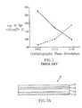
- On the other hand, hole mobilities on (110) Si are 2× higher than on (100) Si; therefore, PFETs formed on a (110) surface will exhibit significantly higher drive currents than PFETs formed on a (100) surface. Unfortunately, electron mobilities on (110) Si surfaces are significantly degraded compared to (100) Si surfaces. The electron mobility degradation on a (110) Si surface is shown, for example, in
FIG. 1 . InFIG. 1 , the solid line represents electron mobility, while the dashed line represents hole mobility. - As can be deduced from the above discussion and
FIG. 1 , the (110) Si surface is optimal for PFET devices because of excellent hole mobility, yet such a crystal orientation is completely inappropriate for NFET devices. Instead, the (100) Si surface is optimal for NFET devices since that crystal orientation favors electron mobility. - In view of the above, there is a need for providing integrated semiconductor devices that are formed upon a substrate having different crystal orientations that provide optimal performance for a specific device. That is, there is an overwhelming need to create a substrate which allows one type of device, such as, for example, a PFET, to be formed on a certain crystallographic surface, e.g., a (110) surface, while forming another type of device, such as, for example, an NFET, on another crystallographic surface, e.g., a (100) surface.
- One object of the present invention is to provide a method of integrating semiconductor devices such that different types of devices are formed upon a specific crystal orientation of a bonded substrate that enhances the performance of the device.
- Another object of the present invention is to provide a method of integrating semiconductor devices such that the PFETs are located on a (110) crystallographic plane, while the NFETs are located on a (100) crystallographic plane of a bonded substrate.
- A further object of the present invention is to provide a method of integrating silicon-on-insulator (SOI) technology with complementary metal oxide semiconductor (CMOS) technology using simple and easy processing steps.
- A still further object of the present invention is to provide a method in which one CMOS device will be SOI-like, while the other CMOS device will be bulk-like.
- An even further object of the present invention is to provide a method in which both CMOS devices being integrated are SOI-like.
- A yet even further object of the present invention is to provide a method to integrate strained-silicon NFETs on a (100) crystallographic surface plane with silicon or strained-silicon PFETs on a (110) crystallographic surface plane.
- An additional object of the present invention is to provide a method of integrating different CMOS devices onto a bonded substrate having different crystallographic surface planes wherein isolation regions are formed between the different types of CMOS devices.
- These and other objects and advantages are achieved by utilizing a method that includes the steps of wafer bonding, masking, etching and regrowth of a semiconductor layer. Specifically, the method of the present invention comprises the steps of:
- providing a bonded substrate comprising at least a first semiconductor layer of a first crystallographic orientation and a second semiconductor layer of a second crystallographic orientation separated by an insulating layer, said first
- crystallographic orientation is different from said second crystallographic orientation and said first semiconductor layer lies above said second semiconductor layer;
- protecting a portion of the bonded substrate to define a first device area, while leaving another portion of the bonded substrate unprotected, said unprotected portion of the bonded substrate defining a second device area;
- etching said unprotected portion of the bonded substrate to expose a surface of the second semiconductor layer; regrowing a semiconductor material on said exposed surface of the second semiconductor layer, said semiconductor material having a crystallographic orientation that is the same as the second crystallographic orientation;
- planarizing the bonded substrate containing the semiconductor material so that an upper surface of the first semiconductor layer is substantially planar with an upper surface of the semiconductor material; and
- forming at least one first semiconductor device in said first device region, while forming at least one second semiconductor device on said semiconductor material in said second device area.
- In accordance with the present invention, the first semiconductor device may be a PFET and the first crystallographic orientation may be (110) or (111), while the second semiconductor device may be an NFET and the second crystallographic orientation may be (100) or (111). It is also possible in the present invention, that the first semiconductor device is a NFET and that the second semiconductor device is a PFET. In one embodiment of the present invention, the method further includes forming isolation regions between the first device region and the second device region. In yet another embodiment of the present invention, the semiconductor material comprises an upper layer of strained Si and a lower layer of relaxed SiGe alloy or a SiC alloy.
- Another aspect of the present invention relates to an integrated semiconductor structure containing at least two types of devices, wherein at least one of the devices is formed upon a first crystallographic surface that is optimal for that device, while the other device is formed upon a second crystallographic surface, which is different from the first, that is optimal for the other device. Specifically, the structure of the present invention comprises:
- a bonded substrate comprising a first device region having a first crystallographic orientation and a second device region having a second crystallographic orientation, said first crystallographic orientation is different from said second crystallographic orientation;
- an isolation region separating said first device region from said second device region; and
- at least one first semiconductor device located in said first device region and at least one second semiconductor device located in said second device region.
- In accordance with the present invention, the first semiconductor device may be a PFET and the first crystallographic orientation may be (110) or (111), while the second semiconductor device may be an NFET and the second crystallographic orientation may be (100) or (111). It is also possible in the present invention that the first semiconductor device is an NFET and the second semiconductor device is a PFET. The configuration of the semiconductor devices will be dependent on the crystal orientation of the bonded substrate.
FIG. 1 . is a plot of μeffat Vgs=1V vs. crystallographic orientation for a Si substrate.FIGS. 2A-2F are pictorial representations (through cross sectional views) illustrating the basic processing steps utilized in the present invention in forming integrated CMOS devices on different crystallographic orientation planes of a bonded substrate.FIGS. 3A-3D are pictorial representations of various wafers that may be bonded together and used in the method described inFIGS. 2A-2E .FIGS. 4A-4J are pictorial representations (through cross sectional views) illustrating the basic processing steps used in forming a high performance semiconductor device containing two NFETs formed on a (100) crystallographic surface, and a PFET, which is located between the NFETs, formed on a (110) crystallographic surface.FIGS. 5A-5G are pictorial representations (through cross sectional views) illustrating alternative processing steps used in forming a high performance semiconductor device containing two NFETs formed on a (100) crystallographic surface, and a PFET, which is located between the NFETs, formed on a (110) crystallographic surface.- The present invention, which provides a method of forming different semiconductor devices, such as NFETs and PFETs, onto a bonded substrate having different crystallographic surfaces, will now be described in greater detail by referring to the following discussion as well as the drawings that accompany the present application. In the accompanying drawings, like and correspondence elements are referred to by like reference numerals.
FIG. 2A illustrate a bondedsubstrate 10, i.e., hybrid substrate, which may be employed in the present invention. As shown, bondedsubstrate 10 includes asurface dielectric layer 18, afirst semiconductor layer 16, an insulatinglayer 14, and asecond semiconductor layer 12. The bondedsubstrate 10 may further include an optional third semiconductor layer (not shown) that is located beneath thesecond semiconductor layer 12. In the optional bonded substrate, another insulating layer separates thesecond semiconductor layer 12 from the optional third semiconductor layer.- The
surface dielectric layer 18 of the bondedsubstrate 10 is an oxide, nitride, oxynitride or other insulating layer that is either present in one of the initial wafers before bonding, or formed atop thefirst semiconductor layer 16 after wafer bonding by either a thermal process (i.e., oxidation, nitridation or oxynitridation) or by deposition. Notwithstanding the origin of thesurface dielectric layer 18, thesurface dielectric layer 18 has a thickness of from about 3 to about 500 nm, with a thickness of from about 5 to about 20 nm being more highly preferred. - The
first semiconductor layer 16 is comprised of any semiconducting material including, for example, Si, SiC, SiGe, SiGeC, Ge alloys, GaAs, InAs, InP as well as other III/V or II/VI compound semiconductors.First semiconductor layer 16 may also comprise an SOI layer of a preformed SOI substrate or a layered semiconductor such as, for example, Si/SiGe. Thefirst semiconductor layer 16 is also characterized as having a first crystallographic orientation, which is preferably (110). Although a (110) crystal orientation is preferred, thefirst semiconductor layer 16 may have a (111), or a (100) crystal orientation. - The thickness of the
first semiconductor layer 16 may vary depending on the initial starting wafers used to form the bondedsubstrate 10. Typically, however, thefirst semiconductor layer 16 has a thickness of from about 5 to about 500 nm, with a thickness of from about 5 to about 100 nm being more highly preferred. - The insulating
layer 14 which is located between thefirst semiconductor layer 16 and thesecond semiconductor layer 12 has a variable thickness depending upon the initial wafers used to create the bondedsubstrate 10. Typically, however, the insulatinglayer 14 has a thickness of from about 1 to about 5 nm, with a thickness of from about 5 to about 100 nm being more highly preferred. The insulatinglayer 14 is an oxide or other like insulator material that is formed on one or both of the wafers prior to bonding. - The
second semiconductor layer 12 is comprised of any semiconducting material which may be the same or different from that of thefirst semiconductor layer 16. Thus,second semiconductor layer 12 may include, for example, Si, SiC, SiGe, SiGeC, Ge alloys, GaAs, InAs, InP as well as other III/V or II/VI compound semiconductors.Second semiconductor layer 12 may also comprise an SOI layer of a preformed SOI substrate or a layered semiconductor such as, for example, Si/SiGe. Thesecond semiconductor layer 12 is also characterized as having a second crystallographic orientation, which is different from the first crystallographic orientation. Since thefirst semiconductor layer 16 is preferably a (110) surface, the crystallographic orientation of thesecond semiconductor layer 12 is preferably (100). Although a (100) crystal orientation is preferred, thesecond semiconductor layer 12 may have a (111), or a (110) crystal structure. - The thickness of the
second semiconductor layer 12 may vary depending on the initial starting wafers used to form the bondedsubstrate 10. Typically, however, thesecond semiconductor layer 12 has a thickness of from about 5 nm to about 200 μm, with a thickness of from about 5 to about 100 nm being more highly preferred. - When an optional third semiconductor layer is present, the optional third semiconductor layer may comprise the same or different semiconducting material as that of the
second semiconductor layer 12. The crystal orientation of the optional third semiconductor layer is typically, but not always, the same as the second semiconductor layer. The optional third semiconductor layer is generally thicker than thesecond semiconductor layer 12. When the optional third layer is present, an insulating layer separates the optional third semiconductor layer from the second semiconductor layer. - The bonded
substrate 10 illustrated inFIG. 2A is comprised of two semiconductor wafers that are bonded together. The two wafers used in fabricating the bondedsubstrate 10 may include two SOI wafers (See,FIG. 3A ), wherein one of the wafers, designated as1, includes thefirst semiconductor layer 16 and the other wafer, designated as2 includes thesecond semiconductor 12; an SOI wafer (designated as2) and a bulk semiconductor wafer (designated as1; see,FIG. 3B ); two bulk semiconductor wafers (designated as1 and2, respectively; seeFIG. 3C ) which both contain an insulatinglayer 14 thereon; or an SOI wafer (designated as2) and a bulk wafer (designated as1) which includes anion implant region 11, such as a H2implant region, which can be used to split a portion of at least one of the wafers during bonding (SeeFIG. 3D ). - Bonding is achieved by first bringing the two wafers into intimate contact with other; optionally applying an external force to the contacted wafers; and then heating the two contacted wafers under conditions that are capable of bonding the two wafers together. The heating step may be performed in the presence or absence of an external force. The heating step is typically performed in an inert ambient at a temperature of from about 200° to about 1050° C. for a time period of from about 2 to about 20 hours. More preferably, the bonding is performed at a temperature of from about 200° to about 400° C. for a time period of from about 2 to about 20 hours. The term “inert ambient” is used in the present invention to denote an atmosphere in which an inert gas, such as He, Ar, N2, Xe, Kr or a mixture thereof, is employed. A preferred ambient used during the bonding process is N2.
- In the embodiment where two SOI wafers are employed, some material layers of at least one of the SOI wafers may be removed after bonding utilizing a planarization process such as chemical mechanical polishing (CMP) or grinding and etching. The planarization process stops when
surface dielectric layer 18 is reached. - In the embodiment in which one of the wafers includes an ion implant region, the ion implant region forms a porous region during bonding which causes a portion of the wafer above the ion implant region to break off leaving a bonded wafer such as is shown, for example, in
FIG. 1A . The implant region is typically comprised of H2ions which are implanted into the surface of the wafer utilizing ion implantation conditions that are well known to those skilled in the art. - In the embodiment where the wafers to be bonded do not include a dielectric layer therein, the
surface dielectric layer 18 may be formed atop the bonded wafers by a thermal process, such as oxidation, or by a conventional deposition process such as chemical vapor deposition (CVD), plasma-enhanced CVD, atomic layer deposition, chemical solution deposition as well as other like deposition processes. Mask 20 is then formed on a predetermined portion of the bondedsubstrate 10 ofFIG. 2A so as to protect a portion of the bondedsubstrate 10, while leaving another portion of the bondedsubstrate 10 unprotected. The protected portion of the bondedsubstrate 10 defines afirst device region 22 of the structure, whereas the unprotected portion of the bondedsubstrate 10 defines asecond device area 24. In one embodiment,mask 20 is formed on a predetermined portion of thesurface dielectric layer 18 by applying a photoresist mask to the entire surface of the bondedsubstrate 10. After application of the photoresist mask, the mask is patterned by lithography, which includes the steps of exposing the photoresist to a pattern of radiation and developing the pattern utilizing a resist developer. The resultant structure including themask 20 formed on a predetermined portion of the bondedsubstrate 10 is shown, for example, inFIG. 2B .- In another
embodiment mask 20 is a nitride or oxynitride layer that is formed and patterned utilizing lithography and etching. The nitride oroxynitride mask 20 may be removed after defining the region for the second semiconductor device. - After providing the
mask 20 to the bondedsubstrate 10, the structure is subjected to one or more etching steps so as to expose a surface of thesecond semiconductor layer 12. Specifically, the one or more etching steps used at this point of the present invention removes the unprotected portions of thesurface dielectric layer 18, as well as underlying portions of thefirst semiconductor layer 16, and a portion of the insulatinglayer 14 which separated thefirst semiconductor layer 16 from thesecond semiconductor layer 12. The etching may be performed utilizing a single etching process or multiple etching steps may be employed. The etching used at this point of the present invention may include a dry etching process such as reactive-ion etching, ion beam etching, plasma etching or laser etching, a wet etching process wherein a chemical etchant is employed or any combination thereof. In a preferred embodiment of the present invention, reactive-ion etching (RIE) is used in selectively removing the unprotected portions of thesurface dielectric layer 18, thefirst semiconductor layer 16 and the insulatinglayer 14 in the secondsemiconductor device region 24. The resultant structure after the etching process has been performed is shown, for example, inFIG. 2C . Note that the sidewalls of the protectedfirst device region 22, i.e., thesurface dielectric layer 18, thefirst semiconductor layer 16, the insulatinglayer 14 and thesecond semiconductor layer 12, are exposed after this etching step. As shown, the exposed sidewalls oflayers mask 20. - The
mask 20 is then removed from the structure shown inFIG. 2C utilizing a conventional resist stripping process and then a liner orspacer 25 is formed on the exposed sidewalls. The liner orspacer 25 is formed by deposition and etching. The liner orspacer 25 is comprised of an insulating material such as, for example, an oxide. - After forming the liner or
spacer 25, asemiconductor material 26 is formed on the exposedsecond semiconductor layer 12. In accordance with the present invention,semiconductor material 26 has a crystallographic orientation that is the same as the crystallographic orientation of thesecond semiconductor layer 12. The resultant structure is shown, for example, inFIG. 2D . - The
semiconductor material 26 may comprise any Si-containing semiconductor, such as Si, strained Si, SiGe, SiC, SiGeC or combinations thereof which is capable of being formed utilizing a selective epitaxial growth method. In some preferred embodiments,semiconductor material 26 is comprised of Si. In other preferred embodiments, the semiconductor material is a strained Si layer that is located atop a relaxed SiGe alloy layer. In the present invention,semiconductor material 26 may be referred to as a regrown semiconductor material. - Next, the structure shown in
FIG. 2D is subjected to a planarization process such as chemical mechanical polishing (CMP) or grinding such that the upper surface of thesemiconductor material 26 is substantially planar with the upper surface of thefirst semiconductor layer 16. Note that previously protected portion ofsurface dielectric layer 18 is removed during this planarization process. - After providing the substantially planar surfaces, an
isolation region 27, such as a shallow trench isolation region, is typically formed so as to isolate the firstsemiconductor device region 22 from the secondsemiconductor device region 24. Theisolation region 27 is formed utilizing processing steps that are well known to those skilled in the art including, for example, trench definition and etching; optionally lining the trench with a diffusion barrier; and filling the trench with a trench dielectric such as an oxide. After the trench fill, the structure may be planarized and an optional densification process step may be performed to density the trench dielectric. - The resultant substantially planar structure containing
isolation region 27 is show, for example, inFIG. 2E . As shown, the structure ofFIG. 2B includes an exposedfirst semiconductor layer 16 of a first crystal orientation and an unexposedregrown semiconductor material 26 that has the same crystal orientation as that of thesecond semiconductor layer 12. FIG. 2F shows the integrated structure that is formed after afirst semiconductor device 30 is formed on a portion of thefirst semiconductor layer 16 and asecond semiconductor device 32 is formed on theregrown semiconductor material 26. Despite showing the presence of only one semiconductor device in each device region, the present invention contemplates forming a plurality of each type of device in the specific device region. In accordance with the present invention, the first semiconductor device may be a PFET or a NFET, whereas the second semiconductor device may be a NFET or PFET, with the proviso that the first semiconductor device is different from the second semiconductor device and that the specific device is fabricating on a crystal orientation that provides a high performance device. The PFETs and NFETs are formed utilizing standard CMOS processing steps that are well known to those skilled in the art. Each FET includes a gate dielectric, a gate conductor, an optional hard mask located atop the gate conductor, spacers located on sidewalls of at least the gate conductor, and source/drain diffusion regions. The diffusion regions are labeled as34 inFIG. 2F . Note that the PFET is formed over the semiconductor material that has a (110), or (111) orientation, whereas the NFET is formed over a semiconductor surface having a (100), or (111) orientation.- The above description and
FIGS. 2A-2F illustrate the basic concept of the present invention which includes providing a bonded substrate having two different crystallographic orientations, masking, etching, regrowth, planarization and device formation. The following description with references toFIGS. 4A-4J illustrate processing steps used in forming a high performance semiconductor device containing two NFETs formed on a (100) crystallographic surface, and a PFET, which is located between the NFETs, formed on a (110) crystallographic surface. FIG. 4A illustrates a bondedsubstrate 10 that may be used in this embodiment of the present invention. The bondedsubstrate 10 includes asurface dielectric layer 18, afirst semiconductor layer 16, an insulatinglayer 14 and asecond semiconductor layer 12. A third optional semiconductor layer may be located beneath thesecond semiconductor layer 12. In such an embodiment, an insulating layer separates the second semiconductor layer from the optional third semiconductor layer.FIG. 4B illustrates the structure afternitride mask 20 has been formed on thesurface dielectric layer 18. Thenitride mask 20 is formed utilizing a conventional deposition process such as CVD.- After formation of
nitride mask 20, the mask is patterned utilizing a patterned photoresist mask and etching, and then the pattern is transferred via another etching process fromnitride mask 20 into the structure stopping atop an upper surface layer of thesecond semiconductor layer 12. The etching used in the second etching removes portions of thesurface dielectric layer 18, thefirst semiconductor layer 16, and the insulatinglayer 14. A single or multiple etching process is performed in transferring the pattern into the bondedsubstrate 10.FIG. 4C shows the resultant structure after pattern transfer. - Next, and as shown in
FIG. 4D ,spacers 25 are formed on the exposed sidewalls. Thespacers 25 are composed of an insulating material including, for example, an oxide. Thespacers 25 which are located on the sidewalls of the protected first device region are formed by deposition and etching. - After formation of the
spacers 25,semiconductor material 26 is formed on the exposed surface of thesecond semiconductor layer 12 providing the structure shown, for example, inFIG. 4E . The structure illustrated inFIG. 4E is then planarized to provide the substantially planer structure shown inFIG. 4F . Note that the planarization step removes thenitride mask 20 and thesurface dielectric layer 18 that were not previously etched so as to provide a structure in whichfirst semiconductor layer 16 is exposed and regrownsemiconductor material 26 is exposed. The exposedfirst semiconductor layer 16 is the region in which a first semiconductor device such as an NFET will be formed, whereas the exposed surface ofsemiconductor material 26 is the region in which a second semiconductor device, such as a PFET, will be formed. - Next, and as shown in
FIG. 4G , amaterial stack 50 comprising apad oxide 51 and apad nitride 52 is then formed atop the substantially planar structure shown inFIG. 4F . Thepad oxide 51 of thematerial stack 50 is formed by either a thermal oxidation process or by deposition, while thepad nitride 52 is formed by a thermal nitridation process or deposition. Thepad nitride 52 is typically thicker than theunderlying pad oxide 51. - The
material stack 50 is used in defining the trench openings forisolation regions 27.FIG. 4H illustrates the structure that is formed aftertrench openings 29 have been formed into the structure shown inFIG. 4G . Thetrench openings 29 are formed by lithography and etching. - After defining the
trench openings 29, thetrench openings 29 are filled with a trench dielectric such as an oxide and planarized to thefirst semiconductor layer 16 and theregrown semiconductor material 26.FIG. 4I shows the structure that is formed after trench filling and planarization. The structure shown inFIG. 4I includes three device regions; two of which are referred to asfirst device regions 22 in which afirst semiconductor device 30 will be formed and the third is asecond device region 24 in which asecond semiconductor device 32 will be formed. FIG. 4J shows the integrated structure that is formed after afirst semiconductor device 30 is formed on a portion of thefirst semiconductor layer 16 and asecond semiconductor device 32 is formed on theregrown semiconductor material 26. Despite showing the presence of only one semiconductor device in each device region, the present invention contemplates forming a plurality of each type of device in the specific device region. In accordance with the present invention, the first semiconductor device may be a PFET (or NFET), whereas the second semiconductor device may be a NFET (or PFET). The PFETs and NFETs are formed utilizing standard CMOS processing steps that are well known to those skilled in the art. Each FET includes a gate dielectric, a gate conductor, an optional hard mask located atop the gate conductor, spacers located on sidewalls of at least the gate conductor, source/drain diffusion regions. Note that the PFET is formed over a surface having a (110) or (111) orientation, whereas the NFET is formed over a surface having a (100) or (111) orientation. In the structure shown inFIG. 4J , the NFETs are SOI-like devices, whereas the PFET is a bulk-like semiconductor device. If a third semiconductor layer was present beneath thesecond semiconductor layer 12, all three devices would be SOI-like.FIGS. 5A-5G illustrates alternative processing steps used in forming a high performance semiconductor device containing two NFETs formed on a (100) crystallographic surface, and a PFET, which is located between the NFETs, formed on a (110) crystallographic surface. The alternative method begins with forming the bonded substrate shown inFIG. 5A . The bondedsubstrate 10 includes at least asurface dielectric layer 18, afirst semiconductor layer 16, an insulatinglayer 14 and asecond semiconductor layer 12. A third optional semiconductor layer may be located beneath the second semiconductor layer.- Next,
nitride mask 20 is formed on the bondedsubstrate 10 to provide the structure illustrated inFIG. 5B . After forming thenitride mask 20 on the bondedsubstrate 10,isolation regions 27 are formed utilizing thenitride mask 20 and surface dielectric18 as a combined etch mask.Isolation regions 27 are formed by applying a photoresist to the surface of thenitride mask 20, patterning the photoresist and transferring the pattern from the photoresist into thenitride mask 20 and then into thesurface dielectric layer 18 to expose thefirst semiconductor layer 16. The exposedfirst semiconductor layer 16 is then etched stopping on an upper surface of the insulatinglayer 14. The trenches formed by the etching step are then filled with a trench dielectric and planarized to an upper surface of thenitride mask 20.FIG. 5C shows the structure after trench fill and planarization. In particular,isolation regions 27 are shown inFIG. 5C . - The material between the isolation regions is then removed providing the structure shown in
FIG. 5D . Specifically, the material between the isolation regions is removed by forming a block mask to protect portions of the structure in which the first semiconductor devices will be formed and then etching the unprotected portions of thenitride mask 20, thesurface dielectric layer 18 and thefirst semiconductor layer 16 stopping on the insulatinglayer 14. - The exposed portion of the insulating
layer 14 is then removed utilizing an etching process that selectively removes an insulator material, such as an oxide, providing the structure shown, for example, inFIG. 5E . Note that this etching step also reduces the height ofisolation regions 27. This etching step stops atop an upper surface of thesecond semiconductor layer 12. The remainingnitride mask 20 is then stripped from the structure and thensemiconductor material 26 is regrown on the exposed surface of thesecond semiconductor material 12 providing the structure shown, for example, inFIG. 5F . In this particular embodiment, theregrown semiconductor material 26 includes an upper layer ofstrained Si 31. - Oxide is then stripped from the structure shown in
FIG. 5F andstrained Si 31 is formed on the exposed portions of thefirst semiconductor layer 16. After forming the strained Si layers,CMOS devices FIG. 5G . - While the present invention has been particularly shown and described with respect to preferred embodiments thereof, it will be understood by those skilled in the art that the foregoing and other changes in forms and details may be made without departing from the spirit and scope of the present invention. It is therefore intended that the present invention not be limited to the exact forms and details described and illustrated, but fall within the scope of the appended claims.
Claims (17)
1. A method of forming CMOS devices on a hybrid crystal oriented substrate comprising:
providing a bonded substrate comprising at least a first semiconductor layer of a first crystallographic orientation and a second semiconductor layer of a second crystallographic orientation separated by an insulating layer, said first crystallographic orientation is different from said second crystallographic orientation and said first semiconductor layer lies above said second semiconductor layer;
protecting a portion of the bonded substrate to define a first device area, while leaving another portion of the bonded substrate unprotected, said unprotected portion of the bonded substrate defining a second device area;
etching said unprotected portion of the bonded substrate to expose a surface of the second semiconductor layer;
regrowing a semiconductor material on said exposed surface of the second semiconductor layer, said semiconductor material having a crystallographic orientation that is the same as the second crystallographic orientation;
planarizing the bonded substrate containing the semiconductor material so that an upper surface of the first semiconductor layer is substantially planar with an upper surface of the semiconductor material; and
forming at least one first semiconductor device in said first device region, while forming at least one second semiconductor device on said semiconductor material in said second device area.
2. The method ofclaim 1 wherein said bonded substrate further comprising a surface dielectric layer located on said first semiconductor material.
3. The method ofclaim 1 wherein said bonded substrate is formed from two silicon-on-insulator (SOI) wafers, a SOI wafer and a bulk semiconductor wafer, two bulk semiconductor wafers, or a SOI wafer and a bulk semiconductor wafer which contains an ion implant region which forms voids after heating.
4. The method ofclaim 1 wherein said bonded substrate is formed by bringing two wafers into intimate contact with each other and heating the contacted wafers in an inert ambient.
5. The method ofclaim 4 wherein said heating is performed at a temperature of from about 200° C. to about 1050° C. for a time period of from about 2 to about 20 hours.
6. The method ofclaim 1 wherein said protecting comprises the use of a patterned mask.
7. The method ofclaim 6 wherein said patterned mask is a patterned photoresist, a patterned nitride or a patterned oxynitride.
8. The method ofclaim 1 wherein said semiconductor material is formed utilizing a selective epitaxial growth method.
9. The method ofclaim 1 wherein said semiconductor material is a Si-containing semiconductor selected from the group consisting of Si, strained Si, SiGe, SiC, SiGeC and combinations thereof.
10. The method ofclaim 1 wherein said planarizing comprises chemical mechanical polishing or grinding.
11. The method ofclaim 1 wherein between said etching and regrowing steps a liner or spacer is formed on exposed sidewalls.
12. The method ofclaim 1 further comprising forming isolation regions after etching, but prior to forming the at least one semiconductor devices.
13. The method ofclaim 1 wherein said semiconductor devices are NFETs or PFETs.
14. The method ofclaim 1 wherein said first semiconductor layer has a (110) crystal orientation and said second semiconductor layer and the semiconductor material both have a (100) crystal orientation.
15. The method ofclaim 14 wherein first semiconductor device is a PFET and the second semiconductor device is an NFET.
16. The method ofclaim 1 wherein said semiconductor devices are formed upon a layer of strained Si.
17. The method ofclaim 1 wherein said semiconductor material comprises a strained Si layer located atop a relaxed SiGe alloy layer.
Priority Applications (1)
| Application Number | Priority Date | Filing Date | Title |
|---|---|---|---|
| US11/958,877US7713807B2 (en) | 2003-06-17 | 2007-12-18 | High-performance CMOS SOI devices on hybrid crystal-oriented substrates |
Applications Claiming Priority (2)
| Application Number | Priority Date | Filing Date | Title |
|---|---|---|---|
| US10/250,241US7329923B2 (en) | 2003-06-17 | 2003-06-17 | High-performance CMOS devices on hybrid crystal oriented substrates |
| US11/958,877US7713807B2 (en) | 2003-06-17 | 2007-12-18 | High-performance CMOS SOI devices on hybrid crystal-oriented substrates |
Related Parent Applications (1)
| Application Number | Title | Priority Date | Filing Date |
|---|---|---|---|
| US10/250,241DivisionUS7329923B2 (en) | 2003-06-17 | 2003-06-17 | High-performance CMOS devices on hybrid crystal oriented substrates |
Publications (2)
| Publication Number | Publication Date |
|---|---|
| US20080096330A1true US20080096330A1 (en) | 2008-04-24 |
| US7713807B2 US7713807B2 (en) | 2010-05-11 |
Family
ID=33516805
Family Applications (2)
| Application Number | Title | Priority Date | Filing Date |
|---|---|---|---|
| US10/250,241Expired - Fee RelatedUS7329923B2 (en) | 2003-06-17 | 2003-06-17 | High-performance CMOS devices on hybrid crystal oriented substrates |
| US11/958,877Expired - Fee RelatedUS7713807B2 (en) | 2003-06-17 | 2007-12-18 | High-performance CMOS SOI devices on hybrid crystal-oriented substrates |
Family Applications Before (1)
| Application Number | Title | Priority Date | Filing Date |
|---|---|---|---|
| US10/250,241Expired - Fee RelatedUS7329923B2 (en) | 2003-06-17 | 2003-06-17 | High-performance CMOS devices on hybrid crystal oriented substrates |
Country Status (8)
| Country | Link |
|---|---|
| US (2) | US7329923B2 (en) |
| EP (1) | EP1639637A1 (en) |
| JP (1) | JP4931211B2 (en) |
| KR (1) | KR100843489B1 (en) |
| CN (1) | CN100407408C (en) |
| IL (1) | IL172517A0 (en) |
| TW (1) | TWI318785B (en) |
| WO (1) | WO2004114400A1 (en) |
Cited By (2)
| Publication number | Priority date | Publication date | Assignee | Title |
|---|---|---|---|---|
| US20090236663A1 (en)* | 2008-03-19 | 2009-09-24 | Chartered Semiconductor Manufacturing, Ltd. | Hybrid orientation substrate with stress layer |
| US8476706B1 (en)* | 2012-01-04 | 2013-07-02 | International Business Machines Corporation | CMOS having a SiC/SiGe alloy stack |
Families Citing this family (158)
| Publication number | Priority date | Publication date | Assignee | Title |
|---|---|---|---|---|
| US7023055B2 (en)* | 2003-10-29 | 2006-04-04 | International Business Machines Corporation | CMOS on hybrid substrate with different crystal orientations using silicon-to-silicon direct wafer bonding |
| US20050116290A1 (en)* | 2003-12-02 | 2005-06-02 | De Souza Joel P. | Planar substrate with selected semiconductor crystal orientations formed by localized amorphization and recrystallization of stacked template layers |
| US7087965B2 (en)* | 2004-04-22 | 2006-08-08 | International Business Machines Corporation | Strained silicon CMOS on hybrid crystal orientations |
| US7208815B2 (en)* | 2004-05-28 | 2007-04-24 | Taiwan Semiconductor Manufacturing Company, Ltd. | CMOS logic gate fabricated on hybrid crystal orientations and method of forming thereof |
| US7125785B2 (en) | 2004-06-14 | 2006-10-24 | International Business Machines Corporation | Mixed orientation and mixed material semiconductor-on-insulator wafer |
| US7291886B2 (en) | 2004-06-21 | 2007-11-06 | International Business Machines Corporation | Hybrid substrate technology for high-mobility planar and multiple-gate MOSFETs |
| TWI463526B (en)* | 2004-06-24 | 2014-12-01 | Ibm | Method for improving stress-induced CMOS components and components prepared by the method |
| DE102004031708B4 (en)* | 2004-06-30 | 2008-02-07 | Advanced Micro Devices, Inc., Sunnyvale | Method for producing a substrate with crystalline semiconductor regions of different properties |
| US7172930B2 (en)* | 2004-07-02 | 2007-02-06 | International Business Machines Corporation | Strained silicon-on-insulator by anodization of a buried p+ silicon germanium layer |
| US7002214B1 (en)* | 2004-07-30 | 2006-02-21 | International Business Machines Corporation | Ultra-thin body super-steep retrograde well (SSRW) FET devices |
| US7274073B2 (en)* | 2004-10-08 | 2007-09-25 | International Business Machines Corporation | Integrated circuit with bulk and SOI devices connected with an epitaxial region |
| US7141457B2 (en) | 2004-11-18 | 2006-11-28 | International Business Machines Corporation | Method to form Si-containing SOI and underlying substrate with different orientations |
| DE102004057764B4 (en) | 2004-11-30 | 2013-05-16 | Advanced Micro Devices, Inc. | A method of fabricating a substrate having crystalline semiconductor regions having different properties disposed over a crystalline bulk substrate and semiconductor device fabricated therewith |
| US7405436B2 (en)* | 2005-01-05 | 2008-07-29 | International Business Machines Corporation | Stressed field effect transistors on hybrid orientation substrate |
| US8138061B2 (en)* | 2005-01-07 | 2012-03-20 | International Business Machines Corporation | Quasi-hydrophobic Si-Si wafer bonding using hydrophilic Si surfaces and dissolution of interfacial bonding oxide |
| US7285473B2 (en)* | 2005-01-07 | 2007-10-23 | International Business Machines Corporation | Method for fabricating low-defect-density changed orientation Si |
| US7271043B2 (en)* | 2005-01-18 | 2007-09-18 | International Business Machines Corporation | Method for manufacturing strained silicon directly-on-insulator substrate with hybrid crystalline orientation and different stress levels |
| US7220626B2 (en)* | 2005-01-28 | 2007-05-22 | International Business Machines Corporation | Structure and method for manufacturing planar strained Si/SiGe substrate with multiple orientations and different stress levels |
| US7298009B2 (en)* | 2005-02-01 | 2007-11-20 | Infineon Technologies Ag | Semiconductor method and device with mixed orientation substrate |
| US20060175659A1 (en)* | 2005-02-07 | 2006-08-10 | International Business Machines Corporation | A cmos structure for body ties in ultra-thin soi (utsoi) substrates |
| JP2006237448A (en)* | 2005-02-28 | 2006-09-07 | Nec Electronics Corp | Method of manufacturing complementary field effect transistor |
| US6972478B1 (en)* | 2005-03-07 | 2005-12-06 | Advanced Micro Devices, Inc. | Integrated circuit and method for its manufacture |
| US7388278B2 (en) | 2005-03-24 | 2008-06-17 | International Business Machines Corporation | High performance field effect transistors on SOI substrate with stress-inducing material as buried insulator and methods |
| WO2006103491A1 (en)* | 2005-03-29 | 2006-10-05 | S.O.I.Tec Silicon On Insulator Technologies | Hybrid fully soi-type multilayer structure |
| US7605429B2 (en) | 2005-04-15 | 2009-10-20 | International Business Machines Corporation | Hybrid crystal orientation CMOS structure for adaptive well biasing and for power and performance enhancement |
| US7274072B2 (en)* | 2005-04-15 | 2007-09-25 | International Business Machines Corporation | Hybrid bulk-SOI 6T-SRAM cell for improved cell stability and performance |
| US7465992B2 (en)* | 2005-04-27 | 2008-12-16 | International Business Machines Corporation | Field effect transistor with mixed-crystal-orientation channel and source/drain regions |
| CN100345248C (en)* | 2005-05-11 | 2007-10-24 | 华东师范大学 | Preparing method and application of heterobonded wafer |
| US7291539B2 (en)* | 2005-06-01 | 2007-11-06 | International Business Machines Corporation | Amorphization/templated recrystallization method for hybrid orientation substrates |
| US20060272574A1 (en)* | 2005-06-07 | 2006-12-07 | Advanced Micro Devices, Inc. | Methods for manufacturing integrated circuits |
| US7358164B2 (en)* | 2005-06-16 | 2008-04-15 | International Business Machines Corporation | Crystal imprinting methods for fabricating substrates with thin active silicon layers |
| US7439108B2 (en)* | 2005-06-16 | 2008-10-21 | International Business Machines Corporation | Coplanar silicon-on-insulator (SOI) regions of different crystal orientations and methods of making the same |
| US7473985B2 (en)* | 2005-06-16 | 2009-01-06 | International Business Machines Corporation | Hybrid oriented substrates and crystal imprinting methods for forming such hybrid oriented substrates |
| US7432149B2 (en)* | 2005-06-23 | 2008-10-07 | Taiwan Semiconductor Manufacturing Company, Ltd. | CMOS on SOI substrates with hybrid crystal orientations |
| US7611937B2 (en)* | 2005-06-24 | 2009-11-03 | Taiwan Semiconductor Manufacturing Company, Ltd. | High performance transistors with hybrid crystal orientations |
| US7217629B2 (en)* | 2005-07-15 | 2007-05-15 | International Business Machines Corporation | Epitaxial imprinting |
| US7382029B2 (en)* | 2005-07-29 | 2008-06-03 | International Business Machines Corporation | Method and apparatus for improving integrated circuit device performance using hybrid crystal orientations |
| KR100655437B1 (en)* | 2005-08-09 | 2006-12-08 | 삼성전자주식회사 | Semiconductor Wafer and Manufacturing Method Thereof |
| US20070040235A1 (en) | 2005-08-19 | 2007-02-22 | International Business Machines Corporation | Dual trench isolation for CMOS with hybrid orientations |
| US20070048980A1 (en)* | 2005-08-24 | 2007-03-01 | International Business Machines Corporation | Method for post-rie passivation of semiconductor surfaces for epitaxial growth |
| US7737532B2 (en)* | 2005-09-06 | 2010-06-15 | Taiwan Semiconductor Manufacturing Company, Ltd. | Hybrid Schottky source-drain CMOS for high mobility and low barrier |
| DE602005015853D1 (en)* | 2005-09-14 | 2009-09-17 | St Microelectronics Srl | Method for producing a phase change memory arrangement with a uniform heating element height |
| US7605447B2 (en)* | 2005-09-22 | 2009-10-20 | International Business Machines Corporation | Highly manufacturable SRAM cells in substrates with hybrid crystal orientation |
| US7420202B2 (en) | 2005-11-08 | 2008-09-02 | Freescale Semiconductor, Inc. | Electronic device including a transistor structure having an active region adjacent to a stressor layer and a process for forming the electronic device |
| US7986029B2 (en)* | 2005-11-08 | 2011-07-26 | Taiwan Semiconductor Manufacturing Company, Ltd. | Dual SOI structure |
| US7348633B2 (en)* | 2005-11-18 | 2008-03-25 | International Business Machines Corporation | Hybrid crystallographic surface orientation substrate having one or more SOI regions and/or bulk semiconductor regions |
| US7288458B2 (en)* | 2005-12-14 | 2007-10-30 | Freescale Semiconductor, Inc. | SOI active layer with different surface orientation |
| US7569466B2 (en)* | 2005-12-16 | 2009-08-04 | International Business Machines Corporation | Dual metal gate self-aligned integration |
| US7436034B2 (en)* | 2005-12-19 | 2008-10-14 | International Business Machines Corporation | Metal oxynitride as a pFET material |
| US8319285B2 (en) | 2005-12-22 | 2012-11-27 | Infineon Technologies Ag | Silicon-on-insulator chip having multiple crystal orientations |
| US8530355B2 (en) | 2005-12-23 | 2013-09-10 | Infineon Technologies Ag | Mixed orientation semiconductor device and method |
| US7432567B2 (en)* | 2005-12-28 | 2008-10-07 | International Business Machines Corporation | Metal gate CMOS with at least a single gate metal and dual gate dielectrics |
| US20070152276A1 (en)* | 2005-12-30 | 2007-07-05 | International Business Machines Corporation | High performance CMOS circuits, and methods for fabricating the same |
| US7833849B2 (en) | 2005-12-30 | 2010-11-16 | International Business Machines Corporation | Method of fabricating a semiconductor structure including one device region having a metal gate electrode located atop a thinned polygate electrode |
| US7425497B2 (en) | 2006-01-20 | 2008-09-16 | International Business Machines Corporation | Introduction of metal impurity to change workfunction of conductive electrodes |
| US8441000B2 (en)* | 2006-02-01 | 2013-05-14 | International Business Machines Corporation | Heterojunction tunneling field effect transistors, and methods for fabricating the same |
| US7678630B2 (en)* | 2006-02-15 | 2010-03-16 | Infineon Technologies Ag | Strained semiconductor device and method of making same |
| US7531392B2 (en)* | 2006-02-27 | 2009-05-12 | International Business Machines Corporation | Multi-orientation semiconductor-on-insulator (SOI) substrate, and method of fabricating same |
| US7402477B2 (en) | 2006-03-30 | 2008-07-22 | Freescale Semiconductor, Inc. | Method of making a multiple crystal orientation semiconductor device |
| US7396407B2 (en)* | 2006-04-18 | 2008-07-08 | International Business Machines Corporation | Trench-edge-defect-free recrystallization by edge-angle-optimized solid phase epitaxy: method and applications to hybrid orientation substrates |
| US7385257B2 (en)* | 2006-04-26 | 2008-06-10 | International Business Machines Corporation | Hybrid orientation SOI substrates, and method for forming the same |
| US7439110B2 (en)* | 2006-05-19 | 2008-10-21 | International Business Machines Corporation | Strained HOT (hybrid orientation technology) MOSFETs |
| US7436006B2 (en)* | 2006-05-19 | 2008-10-14 | International Business Machines Corporation | Hybrid strained orientated substrates and devices |
| US7435639B2 (en)* | 2006-05-31 | 2008-10-14 | Freescale Semiconductor, Inc. | Dual surface SOI by lateral epitaxial overgrowth |
| US7670928B2 (en)* | 2006-06-14 | 2010-03-02 | Intel Corporation | Ultra-thin oxide bonding for S1 to S1 dual orientation bonding |
| US7803690B2 (en)* | 2006-06-23 | 2010-09-28 | Taiwan Semiconductor Manufacturing Company, Ltd. | Epitaxy silicon on insulator (ESOI) |
| KR100741468B1 (en)* | 2006-07-10 | 2007-07-20 | 삼성전자주식회사 | Semiconductor Device and Forming Method |
| US7893493B2 (en)* | 2006-07-10 | 2011-02-22 | International Business Machines Corproation | Stacking fault reduction in epitaxially grown silicon |
| US7803670B2 (en)* | 2006-07-20 | 2010-09-28 | Freescale Semiconductor, Inc. | Twisted dual-substrate orientation (DSO) substrates |
| US7595232B2 (en)* | 2006-09-07 | 2009-09-29 | International Business Machines Corporation | CMOS devices incorporating hybrid orientation technology (HOT) with embedded connectors |
| US7494918B2 (en)* | 2006-10-05 | 2009-02-24 | International Business Machines Corporation | Semiconductor structures including multiple crystallographic orientations and methods for fabrication thereof |
| US7820501B2 (en)* | 2006-10-11 | 2010-10-26 | International Business Machines Corporation | Decoder for a stationary switch machine |
| US7482209B2 (en)* | 2006-11-13 | 2009-01-27 | International Business Machines Corporation | Hybrid orientation substrate and method for fabrication of thereof |
| US8569858B2 (en) | 2006-12-20 | 2013-10-29 | Freescale Semiconductor, Inc. | Semiconductor device including an active region and two layers having different stress characteristics |
| JP5009124B2 (en)* | 2007-01-04 | 2012-08-22 | コバレントマテリアル株式会社 | Manufacturing method of semiconductor substrate |
| US8741743B2 (en)* | 2007-01-05 | 2014-06-03 | Freescale Semiconductor, Inc. | Integrated assist features for epitaxial growth |
| US7781278B2 (en) | 2007-01-18 | 2010-08-24 | International Business Machines Corporation | CMOS devices having channel regions with a V-shaped trench and hybrid channel orientations, and method for forming the same |
| US7843011B2 (en) | 2007-01-31 | 2010-11-30 | Freescale Semiconductor, Inc. | Electronic device including insulating layers having different strains |
| US7611979B2 (en)* | 2007-02-12 | 2009-11-03 | International Business Machines Corporation | Metal gates with low charge trapping and enhanced dielectric reliability characteristics for high-k gate dielectric stacks |
| FR2913527B1 (en)* | 2007-03-05 | 2009-05-22 | Commissariat Energie Atomique | PROCESS FOR MANUFACTURING A MIXED SUBSTRATE AND USE OF THE SUBSTRATE FOR CARRYING OUT CMOS CIRCUITS |
| US20080248626A1 (en)* | 2007-04-05 | 2008-10-09 | International Business Machines Corporation | Shallow trench isolation self-aligned to templated recrystallization boundary |
| US7651902B2 (en)* | 2007-04-20 | 2010-01-26 | International Business Machines Corporation | Hybrid substrates and methods for forming such hybrid substrates |
| US7750406B2 (en)* | 2007-04-20 | 2010-07-06 | International Business Machines Corporation | Design structure incorporating a hybrid substrate |
| US7547641B2 (en)* | 2007-06-05 | 2009-06-16 | International Business Machines Corporation | Super hybrid SOI CMOS devices |
| FR2913815A1 (en)* | 2007-06-06 | 2008-09-19 | Soitec Silicon On Insulator | Hybrid substrate manufacturing method for telecommunication network, involves forming dielectric/polymer layer on structure, assembling layer with support substrates, and eliminating initial substrate until buried layer is eliminated |
| US20090008725A1 (en)* | 2007-07-03 | 2009-01-08 | International Business Machines Corporation | Method for deposition of an ultra-thin electropositive metal-containing cap layer |
| US20090072312A1 (en)* | 2007-09-14 | 2009-03-19 | Leland Chang | Metal High-K (MHK) Dual Gate Stress Engineering Using Hybrid Orientation (HOT) CMOS |
| US8115254B2 (en) | 2007-09-25 | 2012-02-14 | International Business Machines Corporation | Semiconductor-on-insulator structures including a trench containing an insulator stressor plug and method of fabricating same |
| US7808020B2 (en)* | 2007-10-09 | 2010-10-05 | International Business Machines Corporation | Self-assembled sidewall spacer |
| US8105960B2 (en)* | 2007-10-09 | 2012-01-31 | International Business Machines Corporation | Self-assembled sidewall spacer |
| US7863712B2 (en) | 2007-10-30 | 2011-01-04 | International Business Machines Corporation | Hybrid orientation semiconductor structure with reduced boundary defects and method of forming same |
| US7718496B2 (en)* | 2007-10-30 | 2010-05-18 | International Business Machines Corporation | Techniques for enabling multiple Vt devices using high-K metal gate stacks |
| US8492846B2 (en) | 2007-11-15 | 2013-07-23 | International Business Machines Corporation | Stress-generating shallow trench isolation structure having dual composition |
| US8039401B2 (en)* | 2007-12-14 | 2011-10-18 | Fairchild Semiconductor Corporation | Structure and method for forming hybrid substrate |
| US8211786B2 (en) | 2008-02-28 | 2012-07-03 | International Business Machines Corporation | CMOS structure including non-planar hybrid orientation substrate with planar gate electrodes and method for fabrication |
| US8159040B2 (en)* | 2008-05-13 | 2012-04-17 | International Business Machines Corporation | Metal gate integration structure and method including metal fuse, anti-fuse and/or resistor |
| FR2933234B1 (en)* | 2008-06-30 | 2016-09-23 | S O I Tec Silicon On Insulator Tech | GOODLY DUAL STRUCTURE SUBSTRATE AND METHOD FOR MANUFACTURING THE SAME |
| FR2933235B1 (en)* | 2008-06-30 | 2010-11-26 | Soitec Silicon On Insulator | GOOD-WAY SUBSTRATE AND METHOD FOR MANUFACTURING THE SAME |
| FR2933236B1 (en)* | 2008-06-30 | 2010-11-26 | Soitec Silicon On Insulator | SUBSTRATE COMPRISING DIFFERENT TYPES OF SURFACE, AND METHOD OF MANUFACTURING THE SAME |
| FR2933233B1 (en)* | 2008-06-30 | 2010-11-26 | Soitec Silicon On Insulator | GOOD RESISTANCE HIGH RESISTIVITY SUBSTRATE AND METHOD FOR MANUFACTURING THE SAME |
| JP2011524649A (en)* | 2008-09-03 | 2011-09-01 | エス.オー.アイ.テック シリコン オン インシュレータ テクノロジーズ | Substrates with different types of surfaces and methods for obtaining such substrates |
| JP2010072209A (en)* | 2008-09-17 | 2010-04-02 | Fuji Xerox Co Ltd | Electrostatic charge image developing toner, method for manufacturing electrostatic charge image developing toner, electrostatic charge image developing developer, and image forming device |
| JP2010141263A (en)* | 2008-12-15 | 2010-06-24 | Toshiba Corp | Semiconductor device |
| US8053304B2 (en)* | 2009-02-24 | 2011-11-08 | Taiwan Semiconductor Manufacturing Company, Ltd. | Method of forming high-mobility devices including epitaxially growing a semiconductor layer on a dislocation-blocking layer in a recess formed in a semiconductor substrate |
| US8196475B2 (en)* | 2009-03-16 | 2012-06-12 | Kavlico Corporation | Cointegrated MEMS sensor and method |
| JP5562696B2 (en)* | 2009-03-27 | 2014-07-30 | 株式会社半導体エネルギー研究所 | Method for manufacturing semiconductor device |
| US7855105B1 (en) | 2009-06-18 | 2010-12-21 | International Business Machines Corporation | Planar and non-planar CMOS devices with multiple tuned threshold voltages |
| US8227307B2 (en)* | 2009-06-24 | 2012-07-24 | International Business Machines Corporation | Method for removing threshold voltage adjusting layer with external acid diffusion process |
| US8105892B2 (en)* | 2009-08-18 | 2012-01-31 | International Business Machines Corporation | Thermal dual gate oxide device integration |
| US8022488B2 (en) | 2009-09-24 | 2011-09-20 | International Business Machines Corporation | High-performance FETs with embedded stressors |
| US7943458B2 (en)* | 2009-10-06 | 2011-05-17 | International Business Machines Corporation | Methods for obtaining gate stacks with tunable threshold voltage and scaling |
| US8395216B2 (en)* | 2009-10-16 | 2013-03-12 | Texas Instruments Incorporated | Method for using hybrid orientation technology (HOT) in conjunction with selective epitaxy to form semiconductor devices with regions of different electron and hole mobilities and related apparatus |
| US8288222B2 (en) | 2009-10-20 | 2012-10-16 | International Business Machines Corporation | Application of cluster beam implantation for fabricating threshold voltage adjusted FETs |
| US8035141B2 (en) | 2009-10-28 | 2011-10-11 | International Business Machines Corporation | Bi-layer nFET embedded stressor element and integration to enhance drive current |
| CN102055053B (en)* | 2009-11-04 | 2013-09-04 | 中国科学院半导体研究所 | Bonding technology based method for manufacturing microwave transmission line |
| US8723296B2 (en)* | 2009-12-16 | 2014-05-13 | National Semiconductor Corporation | Stress compensation for large area gallium nitride or other nitride-based structures on semiconductor substrates |
| FR2954584B1 (en)* | 2009-12-22 | 2013-07-19 | Commissariat Energie Atomique | HYBRID SUBSTRATE WITH IMPROVED INSULATION AND METHOD FOR SIMPLIFIED REALIZATION OF A HYBRID SUBSTRATE |
| US8445974B2 (en)* | 2010-01-07 | 2013-05-21 | International Business Machines Corporation | Asymmetric FET including sloped threshold voltage adjusting material layer and method of fabricating same |
| CN102130057B (en)* | 2010-01-14 | 2013-05-01 | 中芯国际集成电路制造(上海)有限公司 | Method for making complementary metal oxide semiconductor device, and structure of complementary metal oxide semiconductor device |
| US8299530B2 (en) | 2010-03-04 | 2012-10-30 | International Business Machines Corporation | Structure and method to fabricate pFETS with superior GIDL by localizing workfunction |
| US8450807B2 (en) | 2010-03-09 | 2013-05-28 | International Business Machines Corporation | MOSFETs with reduced contact resistance |
| US8236660B2 (en) | 2010-04-21 | 2012-08-07 | International Business Machines Corporation | Monolayer dopant embedded stressor for advanced CMOS |
| US8299535B2 (en) | 2010-06-25 | 2012-10-30 | International Business Machines Corporation | Delta monolayer dopants epitaxy for embedded source/drain silicide |
| US8361889B2 (en) | 2010-07-06 | 2013-01-29 | International Business Machines Corporation | Strained semiconductor-on-insulator by addition and removal of atoms in a semiconductor-on-insulator |
| CN102098028A (en)* | 2010-10-14 | 2011-06-15 | 中国科学院上海微系统与信息技术研究所 | Complementary metal-oxide-semiconductor (CMOS) ring oscillator based on mixed crystal orientation silicon on insulator (SOI) technology and manufacturing method thereof |
| US8962417B2 (en) | 2010-10-15 | 2015-02-24 | International Business Machines Corporation | Method and structure for pFET junction profile with SiGe channel |
| US8659054B2 (en) | 2010-10-15 | 2014-02-25 | International Business Machines Corporation | Method and structure for pFET junction profile with SiGe channel |
| US8466473B2 (en) | 2010-12-06 | 2013-06-18 | International Business Machines Corporation | Structure and method for Vt tuning and short channel control with high k/metal gate MOSFETs |
| CN102569395B (en)* | 2010-12-31 | 2014-08-20 | 中国科学院微电子研究所 | Semiconductor device and method of forming the same |
| US8536656B2 (en) | 2011-01-10 | 2013-09-17 | International Business Machines Corporation | Self-aligned contacts for high k/metal gate process flow |
| US8643115B2 (en) | 2011-01-14 | 2014-02-04 | International Business Machines Corporation | Structure and method of Tinv scaling for high κ metal gate technology |
| US8912055B2 (en)* | 2011-05-03 | 2014-12-16 | Imec | Method for manufacturing a hybrid MOSFET device and hybrid MOSFET obtainable thereby |
| CN102790004B (en)* | 2011-05-16 | 2014-06-11 | 中国科学院上海微系统与信息技术研究所 | Preparation method of full-isolation mixed crystal orientation crystal orientation silicon-on-insulator (SOI) |
| CN102226989A (en)* | 2011-06-16 | 2011-10-26 | 中国电子科技集团公司第二十四研究所 | Fabrication method of mixed oriented silicon substrate |
| US8432002B2 (en)* | 2011-06-28 | 2013-04-30 | International Business Machines Corporation | Method and structure for low resistive source and drain regions in a replacement metal gate process flow |
| US8552380B1 (en)* | 2012-05-08 | 2013-10-08 | Cambridge Cmos Sensors Limited | IR detector |
| KR102083495B1 (en)* | 2013-01-07 | 2020-03-02 | 삼성전자 주식회사 | Complementary Metal Oxide Semiconductor device, optical apparatus comprising CMOS device and method of manufacturing the same |
| US9059095B2 (en) | 2013-04-22 | 2015-06-16 | International Business Machines Corporation | Self-aligned borderless contacts using a photo-patternable dielectric material as a replacement contact |
| US8999791B2 (en) | 2013-05-03 | 2015-04-07 | International Business Machines Corporation | Formation of semiconductor structures with variable gate lengths |
| US9214567B2 (en) | 2013-09-06 | 2015-12-15 | Globalfoundries Inc. | Nanowire compatible E-fuse |
| EP2849219A1 (en)* | 2013-09-11 | 2015-03-18 | IMEC vzw | Method for manufacturing transistors and associated substrate |
| US8951868B1 (en) | 2013-11-05 | 2015-02-10 | International Business Machines Corporation | Formation of functional gate structures with different critical dimensions using a replacement gate process |
| KR102203033B1 (en)* | 2013-12-18 | 2021-01-14 | 인텔 코포레이션 | Planar heterogeneous device |
| US9595525B2 (en) | 2014-02-10 | 2017-03-14 | International Business Machines Corporation | Semiconductor device including nanowire transistors with hybrid channels |
| US9093425B1 (en) | 2014-02-11 | 2015-07-28 | International Business Machines Corporation | Self-aligned liner formed on metal semiconductor alloy contacts |
| US20150263040A1 (en)* | 2014-03-17 | 2015-09-17 | Silicon Storage Technology, Inc. | Embedded Memory Device With Silicon-On-Insulator Substrate, And Method Of Making Same |
| US9184290B2 (en) | 2014-04-02 | 2015-11-10 | International Business Machines Corporation | Method of forming well-controlled extension profile in MOSFET by silicon germanium based sacrificial layer |
| US9293375B2 (en) | 2014-04-24 | 2016-03-22 | International Business Machines Corporation | Selectively grown self-aligned fins for deep isolation integration |
| US9331076B2 (en) | 2014-05-02 | 2016-05-03 | International Business Machines Corporation | Group III nitride integration with CMOS technology |
| US10056293B2 (en)* | 2014-07-18 | 2018-08-21 | International Business Machines Corporation | Techniques for creating a local interconnect using a SOI wafer |
| US9412840B1 (en) | 2015-05-06 | 2016-08-09 | International Business Machines Corporation | Sacrificial layer for replacement metal semiconductor alloy contact formation |
| US10062693B2 (en)* | 2016-02-24 | 2018-08-28 | International Business Machines Corporation | Patterned gate dielectrics for III-V-based CMOS circuits |
| US10593600B2 (en) | 2016-02-24 | 2020-03-17 | International Business Machines Corporation | Distinct gate stacks for III-V-based CMOS circuits comprising a channel cap |
| FR3051596B1 (en)* | 2016-05-17 | 2022-11-18 | Soitec Silicon On Insulator | METHOD FOR MANUFACTURING A STRESSED-ON-INSULATOR SEMICONDUCTOR-TYPE SUBSTRATE |
| CN107507806B (en)* | 2016-06-14 | 2020-06-05 | 西安电子科技大学 | Compressive strained Si CMOS device based on channel crystal orientation selection and its preparation method |
| JP6763703B2 (en)* | 2016-06-17 | 2020-09-30 | ラピスセミコンダクタ株式会社 | Semiconductor devices and methods for manufacturing semiconductor devices |
| US12020980B2 (en)* | 2021-07-07 | 2024-06-25 | Taiwan Semiconductor Manufacturing Company, Ltd. | Semiconductor structure and forming method thereof |
| CN116344448A (en)* | 2021-12-17 | 2023-06-27 | 苏州龙驰半导体科技有限公司 | Manufacturing method of semiconductor device and semiconductor device |
Citations (68)
| Publication number | Priority date | Publication date | Assignee | Title |
|---|---|---|---|---|
| US3602841A (en)* | 1970-06-18 | 1971-08-31 | Ibm | High frequency bulk semiconductor amplifiers and oscillators |
| US4442448A (en)* | 1979-10-26 | 1984-04-10 | Seiko Instruments & Electronics Ltd. | Logic integrated circuit device |
| US4507158A (en)* | 1983-08-12 | 1985-03-26 | Hewlett-Packard Co. | Trench isolated transistors in semiconductor films |
| US4665415A (en)* | 1985-04-24 | 1987-05-12 | International Business Machines Corporation | Semiconductor device with hole conduction via strained lattice |
| US4853076A (en)* | 1983-12-29 | 1989-08-01 | Massachusetts Institute Of Technology | Semiconductor thin films |
| US4855245A (en)* | 1985-09-13 | 1989-08-08 | Siemens Aktiengesellschaft | Method of manufacturing integrated circuit containing bipolar and complementary MOS transistors on a common substrate |
| US4878957A (en)* | 1988-03-31 | 1989-11-07 | Kabushiki Kaisha Toshiba | Dielectrically isolated semiconductor substrate |
| US4952524A (en)* | 1989-05-05 | 1990-08-28 | At&T Bell Laboratories | Semiconductor device manufacture including trench formation |
| US4958213A (en)* | 1987-12-07 | 1990-09-18 | Texas Instruments Incorporated | Method for forming a transistor base region under thick oxide |
| US5006913A (en)* | 1988-11-05 | 1991-04-09 | Mitsubishi Denki Kabushiki Kaisha | Stacked type semiconductor device |
| US5060030A (en)* | 1990-07-18 | 1991-10-22 | Raytheon Company | Pseudomorphic HEMT having strained compensation layer |
| US5081513A (en)* | 1991-02-28 | 1992-01-14 | Xerox Corporation | Electronic device with recovery layer proximate to active layer |
| US5108843A (en)* | 1988-11-30 | 1992-04-28 | Ricoh Company, Ltd. | Thin film semiconductor and process for producing the same |
| US5134085A (en)* | 1991-11-21 | 1992-07-28 | Micron Technology, Inc. | Reduced-mask, split-polysilicon CMOS process, incorporating stacked-capacitor cells, for fabricating multi-megabit dynamic random access memories |
| US5310446A (en)* | 1990-01-10 | 1994-05-10 | Ricoh Company, Ltd. | Method for producing semiconductor film |
| US5354695A (en)* | 1992-04-08 | 1994-10-11 | Leedy Glenn J | Membrane dielectric isolation IC fabrication |
| US5371399A (en)* | 1991-06-14 | 1994-12-06 | International Business Machines Corporation | Compound semiconductor having metallic inclusions and devices fabricated therefrom |
| US5384473A (en)* | 1991-10-01 | 1995-01-24 | Kabushiki Kaisha Toshiba | Semiconductor body having element formation surfaces with different orientations |
| US5391510A (en)* | 1992-02-28 | 1995-02-21 | International Business Machines Corporation | Formation of self-aligned metal gate FETs using a benignant removable gate material during high temperature steps |
| US5459346A (en)* | 1988-06-28 | 1995-10-17 | Ricoh Co., Ltd. | Semiconductor substrate with electrical contact in groove |
| US5471918A (en)* | 1995-01-30 | 1995-12-05 | Hsieh; Li-Tsu | No-load-run strap release control mechanism for a strapping machine |
| US5557122A (en)* | 1995-05-12 | 1996-09-17 | Alliance Semiconductors Corporation | Semiconductor electrode having improved grain structure and oxide growth properties |
| US5561302A (en)* | 1994-09-26 | 1996-10-01 | Motorola, Inc. | Enhanced mobility MOSFET device and method |
| US5670798A (en)* | 1995-03-29 | 1997-09-23 | North Carolina State University | Integrated heterostructures of Group III-V nitride semiconductor materials including epitaxial ohmic contact non-nitride buffer layer and methods of fabricating same |
| US5679965A (en)* | 1995-03-29 | 1997-10-21 | North Carolina State University | Integrated heterostructures of Group III-V nitride semiconductor materials including epitaxial ohmic contact, non-nitride buffer layer and methods of fabricating same |
| US5847419A (en)* | 1996-09-17 | 1998-12-08 | Kabushiki Kaisha Toshiba | Si-SiGe semiconductor device and method of fabricating the same |
| US5861651A (en)* | 1997-02-28 | 1999-01-19 | Lucent Technologies Inc. | Field effect devices and capacitors with improved thin film dielectrics and method for making same |
| US5880040A (en)* | 1996-04-15 | 1999-03-09 | Macronix International Co., Ltd. | Gate dielectric based on oxynitride grown in N2 O and annealed in NO |
| US5940736A (en)* | 1997-03-11 | 1999-08-17 | Lucent Technologies Inc. | Method for forming a high quality ultrathin gate oxide layer |
| US5989978A (en)* | 1998-07-16 | 1999-11-23 | Chartered Semiconductor Manufacturing, Ltd. | Shallow trench isolation of MOSFETS with reduced corner parasitic currents |
| US6008126A (en)* | 1992-04-08 | 1999-12-28 | Elm Technology Corporation | Membrane dielectric isolation IC fabrication |
| US6025280A (en)* | 1997-04-28 | 2000-02-15 | Lucent Technologies Inc. | Use of SiD4 for deposition of ultra thin and controllable oxides |
| US6066545A (en)* | 1997-12-09 | 2000-05-23 | Texas Instruments Incorporated | Birdsbeak encroachment using combination of wet and dry etch for isolation nitride |
| US6090684A (en)* | 1998-07-31 | 2000-07-18 | Hitachi, Ltd. | Method for manufacturing semiconductor device |
| US6107143A (en)* | 1998-03-02 | 2000-08-22 | Samsung Electronics Co., Ltd. | Method for forming a trench isolation structure in an integrated circuit |
| US6117722A (en)* | 1999-02-18 | 2000-09-12 | Taiwan Semiconductor Manufacturing Company | SRAM layout for relaxing mechanical stress in shallow trench isolation technology and method of manufacture thereof |
| US6133071A (en)* | 1997-10-15 | 2000-10-17 | Nec Corporation | Semiconductor device with plate heat sink free from cracks due to thermal stress and process for assembling it with package |
| US6165383A (en)* | 1998-04-10 | 2000-12-26 | Organic Display Technology | Useful precursors for organic electroluminescent materials and devices made from such materials |
| US6214694B1 (en)* | 1998-11-17 | 2001-04-10 | International Business Machines Corporation | Process of making densely patterned silicon-on-insulator (SOI) region on a wafer |
| US6221735B1 (en)* | 2000-02-15 | 2001-04-24 | Philips Semiconductors, Inc. | Method for eliminating stress induced dislocations in CMOS devices |
| US6228694B1 (en)* | 1999-06-28 | 2001-05-08 | Intel Corporation | Method of increasing the mobility of MOS transistors by use of localized stress regions |
| US6255169B1 (en)* | 1999-02-22 | 2001-07-03 | Advanced Micro Devices, Inc. | Process for fabricating a high-endurance non-volatile memory device |
| US6261964B1 (en)* | 1997-03-14 | 2001-07-17 | Micron Technology, Inc. | Material removal method for forming a structure |
| US6274444B1 (en)* | 1999-07-30 | 2001-08-14 | United Microelectronics Corp. | Method for forming mosfet |
| US6281532B1 (en)* | 1999-06-28 | 2001-08-28 | Intel Corporation | Technique to obtain increased channel mobilities in NMOS transistors by gate electrode engineering |
| US6284626B1 (en)* | 1999-04-06 | 2001-09-04 | Vantis Corporation | Angled nitrogen ion implantation for minimizing mechanical stress on side walls of an isolation trench |
| US6362082B1 (en)* | 1999-06-28 | 2002-03-26 | Intel Corporation | Methodology for control of short channel effects in MOS transistors |
| US6361885B1 (en)* | 1998-04-10 | 2002-03-26 | Organic Display Technology | Organic electroluminescent materials and device made from such materials |
| US6368931B1 (en)* | 2000-03-27 | 2002-04-09 | Intel Corporation | Thin tensile layers in shallow trench isolation and method of making same |
| US6403975B1 (en)* | 1996-04-09 | 2002-06-11 | Max-Planck Gesellschaft Zur Forderung Der Wissenschafteneev | Semiconductor components, in particular photodetectors, light emitting diodes, optical modulators and waveguides with multilayer structures grown on silicon substrates |
| US6406973B1 (en)* | 1999-06-29 | 2002-06-18 | Hyundai Electronics Industries Co., Ltd. | Transistor in a semiconductor device and method of manufacturing the same |
| US20020086472A1 (en)* | 2000-12-29 | 2002-07-04 | Brian Roberds | Technique to obtain high mobility channels in MOS transistors by forming a strain layer on an underside of a channel |
| US20020090791A1 (en)* | 1999-06-28 | 2002-07-11 | Brian S. Doyle | Method for reduced capacitance interconnect system using gaseous implants into the ild |
| US6429061B1 (en)* | 2000-07-26 | 2002-08-06 | International Business Machines Corporation | Method to fabricate a strained Si CMOS structure using selective epitaxial deposition of Si after device isolation formation |
| US6476462B2 (en)* | 1999-12-28 | 2002-11-05 | Texas Instruments Incorporated | MOS-type semiconductor device and method for making same |
| US6493497B1 (en)* | 2000-09-26 | 2002-12-10 | Motorola, Inc. | Electro-optic structure and process for fabricating same |
| US6498358B1 (en)* | 2001-07-20 | 2002-12-24 | Motorola, Inc. | Structure and method for fabricating an electro-optic system having an electrochromic diffraction grating |
| US6501121B1 (en)* | 2000-11-15 | 2002-12-31 | Motorola, Inc. | Semiconductor structure |
| US6506652B2 (en)* | 1998-11-13 | 2003-01-14 | Intel Corporation | Method of recessing spacers to improved salicide resistance on polysilicon gates |
| US20030040158A1 (en)* | 2001-08-21 | 2003-02-27 | Nec Corporation | Semiconductor device and method of fabricating the same |
| US6531740B2 (en)* | 2001-07-17 | 2003-03-11 | Motorola, Inc. | Integrated impedance matching and stability network |
| US6531369B1 (en)* | 2000-03-01 | 2003-03-11 | Applied Micro Circuits Corporation | Heterojunction bipolar transistor (HBT) fabrication using a selectively deposited silicon germanium (SiGe) |
| US6555891B1 (en)* | 2000-10-17 | 2003-04-29 | International Business Machines Corporation | SOI hybrid structure with selective epitaxial growth of silicon |
| US20030227036A1 (en)* | 2002-02-22 | 2003-12-11 | Naoharu Sugiyama | Semiconductor device |
| US20040018701A1 (en)* | 2002-06-07 | 2004-01-29 | Sharp Kabushiki Kaisha | Manufacturing method for semiconductor substrate and manufacturing method for semiconductor device |
| US6724019B2 (en)* | 2000-05-25 | 2004-04-20 | Renesas Technology Corporation | Multi-layered, single crystal field effect transistor |
| US6870226B2 (en)* | 2002-10-17 | 2005-03-22 | Renesas Technology Corp. | Semiconductor device and method of manufacturing same |
| US6902962B2 (en)* | 2003-04-04 | 2005-06-07 | Taiwan Semiconductor Manufacturing Company, Ltd. | Silicon-on-insulator chip with multiple crystal orientations |
Family Cites Families (21)
| Publication number | Priority date | Publication date | Assignee | Title |
|---|---|---|---|---|
| JPS6292361A (en) | 1985-10-17 | 1987-04-27 | Toshiba Corp | Complementary semiconductor device |
| EP0299560B1 (en) | 1987-07-14 | 1994-09-14 | Agfa-Gevaert N.V. | Process for making a curled photographic film |
| JPH01162362A (en) | 1987-12-18 | 1989-06-26 | Fujitsu Ltd | Manufacturing method of semiconductor device |
| US5173446A (en)* | 1988-06-28 | 1992-12-22 | Ricoh Company, Ltd. | Semiconductor substrate manufacturing by recrystallization using a cooling medium |
| JPH04372166A (en)* | 1991-06-21 | 1992-12-25 | Matsushita Electric Ind Co Ltd | Manufacturing method of semiconductor device |
| WO1994027317A1 (en) | 1993-05-06 | 1994-11-24 | Siemens Aktiengesellschaft | Process for producing components on an soi substrate |
| JPH07183488A (en) | 1993-12-24 | 1995-07-21 | Nissan Motor Co Ltd | MOS-controlled thyristor and method of manufacturing the same |
| US5399507A (en)* | 1994-06-27 | 1995-03-21 | Motorola, Inc. | Fabrication of mixed thin-film and bulk semiconductor substrate for integrated circuit applications |
| JP3372158B2 (en)* | 1996-02-09 | 2003-01-27 | 株式会社東芝 | Semiconductor device and manufacturing method thereof |
| US5610083A (en)* | 1996-05-20 | 1997-03-11 | Chartered Semiconductor Manufacturing Pte Ltd | Method of making back gate contact for silicon on insulator technology |
| JP4521542B2 (en) | 1999-03-30 | 2010-08-11 | ルネサスエレクトロニクス株式会社 | Semiconductor device and semiconductor substrate |
| US6245615B1 (en)* | 1999-08-31 | 2001-06-12 | Micron Technology, Inc. | Method and apparatus on (110) surfaces of silicon structures with conduction in the <110> direction |
| JP4397491B2 (en)* | 1999-11-30 | 2010-01-13 | 財団法人国際科学振興財団 | Semiconductor device using silicon having 111 plane orientation on surface and method of forming the same |
| US7312485B2 (en) | 2000-11-29 | 2007-12-25 | Intel Corporation | CMOS fabrication process utilizing special transistor orientation |
| JP2004531054A (en)* | 2001-03-02 | 2004-10-07 | アンバーウェーブ システムズ コーポレイション | Relaxed silicon germanium platform for high speed CMOS electronics and high speed analog circuits |
| JP2002359293A (en)* | 2001-05-31 | 2002-12-13 | Toshiba Corp | Semiconductor device |
| JP4322453B2 (en)* | 2001-09-27 | 2009-09-02 | 株式会社東芝 | Semiconductor device and manufacturing method thereof |
| US7023055B2 (en)* | 2003-10-29 | 2006-04-04 | International Business Machines Corporation | CMOS on hybrid substrate with different crystal orientations using silicon-to-silicon direct wafer bonding |
| US7087965B2 (en)* | 2004-04-22 | 2006-08-08 | International Business Machines Corporation | Strained silicon CMOS on hybrid crystal orientations |
| US7291886B2 (en)* | 2004-06-21 | 2007-11-06 | International Business Machines Corporation | Hybrid substrate technology for high-mobility planar and multiple-gate MOSFETs |
| US7253034B2 (en)* | 2004-07-29 | 2007-08-07 | International Business Machines Corporation | Dual SIMOX hybrid orientation technology (HOT) substrates |
- 2003
- 2003-06-17USUS10/250,241patent/US7329923B2/ennot_activeExpired - Fee Related
- 2004
- 2004-05-27KRKR1020057021907Apatent/KR100843489B1/ennot_activeExpired - Fee Related
- 2004-05-27EPEP04741667Apatent/EP1639637A1/ennot_activeWithdrawn
- 2004-05-27CNCN2004800234988Apatent/CN100407408C/ennot_activeExpired - Fee Related
- 2004-05-27JPJP2006516124Apatent/JP4931211B2/ennot_activeExpired - Fee Related
- 2004-05-27WOPCT/EP2004/050946patent/WO2004114400A1/enactiveSearch and Examination
- 2004-06-11TWTW093116964Apatent/TWI318785B/ennot_activeIP Right Cessation
- 2005
- 2005-12-12ILIL172517Apatent/IL172517A0/enunknown
- 2007
- 2007-12-18USUS11/958,877patent/US7713807B2/ennot_activeExpired - Fee Related
Patent Citations (81)
| Publication number | Priority date | Publication date | Assignee | Title |
|---|---|---|---|---|
| US3602841A (en)* | 1970-06-18 | 1971-08-31 | Ibm | High frequency bulk semiconductor amplifiers and oscillators |
| US4442448A (en)* | 1979-10-26 | 1984-04-10 | Seiko Instruments & Electronics Ltd. | Logic integrated circuit device |
| US4507158A (en)* | 1983-08-12 | 1985-03-26 | Hewlett-Packard Co. | Trench isolated transistors in semiconductor films |
| US4853076A (en)* | 1983-12-29 | 1989-08-01 | Massachusetts Institute Of Technology | Semiconductor thin films |
| US4665415A (en)* | 1985-04-24 | 1987-05-12 | International Business Machines Corporation | Semiconductor device with hole conduction via strained lattice |
| US4855245A (en)* | 1985-09-13 | 1989-08-08 | Siemens Aktiengesellschaft | Method of manufacturing integrated circuit containing bipolar and complementary MOS transistors on a common substrate |
| US4958213A (en)* | 1987-12-07 | 1990-09-18 | Texas Instruments Incorporated | Method for forming a transistor base region under thick oxide |
| US4878957A (en)* | 1988-03-31 | 1989-11-07 | Kabushiki Kaisha Toshiba | Dielectrically isolated semiconductor substrate |
| US5565697A (en)* | 1988-06-28 | 1996-10-15 | Ricoh Company, Ltd. | Semiconductor structure having island forming grooves |
| US5459346A (en)* | 1988-06-28 | 1995-10-17 | Ricoh Co., Ltd. | Semiconductor substrate with electrical contact in groove |
| US5006913A (en)* | 1988-11-05 | 1991-04-09 | Mitsubishi Denki Kabushiki Kaisha | Stacked type semiconductor device |
| US5108843A (en)* | 1988-11-30 | 1992-04-28 | Ricoh Company, Ltd. | Thin film semiconductor and process for producing the same |
| US4952524A (en)* | 1989-05-05 | 1990-08-28 | At&T Bell Laboratories | Semiconductor device manufacture including trench formation |
| US5310446A (en)* | 1990-01-10 | 1994-05-10 | Ricoh Company, Ltd. | Method for producing semiconductor film |
| US5060030A (en)* | 1990-07-18 | 1991-10-22 | Raytheon Company | Pseudomorphic HEMT having strained compensation layer |
| US5081513A (en)* | 1991-02-28 | 1992-01-14 | Xerox Corporation | Electronic device with recovery layer proximate to active layer |
| US5371399A (en)* | 1991-06-14 | 1994-12-06 | International Business Machines Corporation | Compound semiconductor having metallic inclusions and devices fabricated therefrom |
| US5384473A (en)* | 1991-10-01 | 1995-01-24 | Kabushiki Kaisha Toshiba | Semiconductor body having element formation surfaces with different orientations |
| US5134085A (en)* | 1991-11-21 | 1992-07-28 | Micron Technology, Inc. | Reduced-mask, split-polysilicon CMOS process, incorporating stacked-capacitor cells, for fabricating multi-megabit dynamic random access memories |
| US5391510A (en)* | 1992-02-28 | 1995-02-21 | International Business Machines Corporation | Formation of self-aligned metal gate FETs using a benignant removable gate material during high temperature steps |
| US5840593A (en)* | 1992-04-08 | 1998-11-24 | Elm Technology Corporation | Membrane dielectric isolation IC fabrication |
| US5354695A (en)* | 1992-04-08 | 1994-10-11 | Leedy Glenn J | Membrane dielectric isolation IC fabrication |
| US6008126A (en)* | 1992-04-08 | 1999-12-28 | Elm Technology Corporation | Membrane dielectric isolation IC fabrication |
| US5946559A (en)* | 1992-04-08 | 1999-08-31 | Elm Technology Corporation | Membrane dielectric isolation IC fabrication |
| US5571741A (en)* | 1992-04-08 | 1996-11-05 | Leedy; Glenn J. | Membrane dielectric isolation IC fabrication |
| US5592018A (en)* | 1992-04-08 | 1997-01-07 | Leedy; Glenn J. | Membrane dielectric isolation IC fabrication |
| US5592007A (en)* | 1992-04-08 | 1997-01-07 | Leedy; Glenn J. | Membrane dielectric isolation transistor fabrication |
| US5683934A (en)* | 1994-09-26 | 1997-11-04 | Motorola, Inc. | Enhanced mobility MOSFET device and method |
| US5561302A (en)* | 1994-09-26 | 1996-10-01 | Motorola, Inc. | Enhanced mobility MOSFET device and method |
| US5471918A (en)* | 1995-01-30 | 1995-12-05 | Hsieh; Li-Tsu | No-load-run strap release control mechanism for a strapping machine |
| US5670798A (en)* | 1995-03-29 | 1997-09-23 | North Carolina State University | Integrated heterostructures of Group III-V nitride semiconductor materials including epitaxial ohmic contact non-nitride buffer layer and methods of fabricating same |
| US5679965A (en)* | 1995-03-29 | 1997-10-21 | North Carolina State University | Integrated heterostructures of Group III-V nitride semiconductor materials including epitaxial ohmic contact, non-nitride buffer layer and methods of fabricating same |
| US6046464A (en)* | 1995-03-29 | 2000-04-04 | North Carolina State University | Integrated heterostructures of group III-V nitride semiconductor materials including epitaxial ohmic contact comprising multiple quantum well |
| US5557122A (en)* | 1995-05-12 | 1996-09-17 | Alliance Semiconductors Corporation | Semiconductor electrode having improved grain structure and oxide growth properties |
| US6403975B1 (en)* | 1996-04-09 | 2002-06-11 | Max-Planck Gesellschaft Zur Forderung Der Wissenschafteneev | Semiconductor components, in particular photodetectors, light emitting diodes, optical modulators and waveguides with multilayer structures grown on silicon substrates |
| US5880040A (en)* | 1996-04-15 | 1999-03-09 | Macronix International Co., Ltd. | Gate dielectric based on oxynitride grown in N2 O and annealed in NO |
| US5847419A (en)* | 1996-09-17 | 1998-12-08 | Kabushiki Kaisha Toshiba | Si-SiGe semiconductor device and method of fabricating the same |
| US5861651A (en)* | 1997-02-28 | 1999-01-19 | Lucent Technologies Inc. | Field effect devices and capacitors with improved thin film dielectrics and method for making same |
| US5940736A (en)* | 1997-03-11 | 1999-08-17 | Lucent Technologies Inc. | Method for forming a high quality ultrathin gate oxide layer |
| US6246095B1 (en)* | 1997-03-11 | 2001-06-12 | Agere Systems Guardian Corp. | System and method for forming a uniform thin gate oxide layer |
| US6261964B1 (en)* | 1997-03-14 | 2001-07-17 | Micron Technology, Inc. | Material removal method for forming a structure |
| US6025280A (en)* | 1997-04-28 | 2000-02-15 | Lucent Technologies Inc. | Use of SiD4 for deposition of ultra thin and controllable oxides |
| US6133071A (en)* | 1997-10-15 | 2000-10-17 | Nec Corporation | Semiconductor device with plate heat sink free from cracks due to thermal stress and process for assembling it with package |
| US6066545A (en)* | 1997-12-09 | 2000-05-23 | Texas Instruments Incorporated | Birdsbeak encroachment using combination of wet and dry etch for isolation nitride |
| US6107143A (en)* | 1998-03-02 | 2000-08-22 | Samsung Electronics Co., Ltd. | Method for forming a trench isolation structure in an integrated circuit |
| US6361885B1 (en)* | 1998-04-10 | 2002-03-26 | Organic Display Technology | Organic electroluminescent materials and device made from such materials |
| US6165383A (en)* | 1998-04-10 | 2000-12-26 | Organic Display Technology | Useful precursors for organic electroluminescent materials and devices made from such materials |
| US5989978A (en)* | 1998-07-16 | 1999-11-23 | Chartered Semiconductor Manufacturing, Ltd. | Shallow trench isolation of MOSFETS with reduced corner parasitic currents |
| US6090684A (en)* | 1998-07-31 | 2000-07-18 | Hitachi, Ltd. | Method for manufacturing semiconductor device |
| US6521964B1 (en)* | 1998-11-13 | 2003-02-18 | Intel Corporation | Device having spacers for improved salicide resistance on polysilicon gates |
| US6509618B2 (en)* | 1998-11-13 | 2003-01-21 | Intel Corporation | Device having thin first spacers and partially recessed thick second spacers for improved salicide resistance on polysilicon gates |
| US6506652B2 (en)* | 1998-11-13 | 2003-01-14 | Intel Corporation | Method of recessing spacers to improved salicide resistance on polysilicon gates |
| US6214694B1 (en)* | 1998-11-17 | 2001-04-10 | International Business Machines Corporation | Process of making densely patterned silicon-on-insulator (SOI) region on a wafer |
| US6117722A (en)* | 1999-02-18 | 2000-09-12 | Taiwan Semiconductor Manufacturing Company | SRAM layout for relaxing mechanical stress in shallow trench isolation technology and method of manufacture thereof |
| US6255169B1 (en)* | 1999-02-22 | 2001-07-03 | Advanced Micro Devices, Inc. | Process for fabricating a high-endurance non-volatile memory device |
| US6284626B1 (en)* | 1999-04-06 | 2001-09-04 | Vantis Corporation | Angled nitrogen ion implantation for minimizing mechanical stress on side walls of an isolation trench |
| US20020090791A1 (en)* | 1999-06-28 | 2002-07-11 | Brian S. Doyle | Method for reduced capacitance interconnect system using gaseous implants into the ild |
| US6362082B1 (en)* | 1999-06-28 | 2002-03-26 | Intel Corporation | Methodology for control of short channel effects in MOS transistors |
| US20020074598A1 (en)* | 1999-06-28 | 2002-06-20 | Doyle Brian S. | Methodology for control of short channel effects in MOS transistors |
| US6281532B1 (en)* | 1999-06-28 | 2001-08-28 | Intel Corporation | Technique to obtain increased channel mobilities in NMOS transistors by gate electrode engineering |
| US6228694B1 (en)* | 1999-06-28 | 2001-05-08 | Intel Corporation | Method of increasing the mobility of MOS transistors by use of localized stress regions |
| US6406973B1 (en)* | 1999-06-29 | 2002-06-18 | Hyundai Electronics Industries Co., Ltd. | Transistor in a semiconductor device and method of manufacturing the same |
| US6274444B1 (en)* | 1999-07-30 | 2001-08-14 | United Microelectronics Corp. | Method for forming mosfet |
| US6476462B2 (en)* | 1999-12-28 | 2002-11-05 | Texas Instruments Incorporated | MOS-type semiconductor device and method for making same |
| US6221735B1 (en)* | 2000-02-15 | 2001-04-24 | Philips Semiconductors, Inc. | Method for eliminating stress induced dislocations in CMOS devices |
| US6531369B1 (en)* | 2000-03-01 | 2003-03-11 | Applied Micro Circuits Corporation | Heterojunction bipolar transistor (HBT) fabrication using a selectively deposited silicon germanium (SiGe) |
| US6368931B1 (en)* | 2000-03-27 | 2002-04-09 | Intel Corporation | Thin tensile layers in shallow trench isolation and method of making same |
| US6724019B2 (en)* | 2000-05-25 | 2004-04-20 | Renesas Technology Corporation | Multi-layered, single crystal field effect transistor |
| US6429061B1 (en)* | 2000-07-26 | 2002-08-06 | International Business Machines Corporation | Method to fabricate a strained Si CMOS structure using selective epitaxial deposition of Si after device isolation formation |
| US6493497B1 (en)* | 2000-09-26 | 2002-12-10 | Motorola, Inc. | Electro-optic structure and process for fabricating same |
| US6555891B1 (en)* | 2000-10-17 | 2003-04-29 | International Business Machines Corporation | SOI hybrid structure with selective epitaxial growth of silicon |
| US6635543B2 (en)* | 2000-10-17 | 2003-10-21 | International Business Machines Corporation | SOI hybrid structure with selective epitaxial growth of silicon |
| US6501121B1 (en)* | 2000-11-15 | 2002-12-31 | Motorola, Inc. | Semiconductor structure |
| US20020086472A1 (en)* | 2000-12-29 | 2002-07-04 | Brian Roberds | Technique to obtain high mobility channels in MOS transistors by forming a strain layer on an underside of a channel |
| US6531740B2 (en)* | 2001-07-17 | 2003-03-11 | Motorola, Inc. | Integrated impedance matching and stability network |
| US6498358B1 (en)* | 2001-07-20 | 2002-12-24 | Motorola, Inc. | Structure and method for fabricating an electro-optic system having an electrochromic diffraction grating |
| US20030040158A1 (en)* | 2001-08-21 | 2003-02-27 | Nec Corporation | Semiconductor device and method of fabricating the same |
| US20030227036A1 (en)* | 2002-02-22 | 2003-12-11 | Naoharu Sugiyama | Semiconductor device |
| US20040018701A1 (en)* | 2002-06-07 | 2004-01-29 | Sharp Kabushiki Kaisha | Manufacturing method for semiconductor substrate and manufacturing method for semiconductor device |
| US6870226B2 (en)* | 2002-10-17 | 2005-03-22 | Renesas Technology Corp. | Semiconductor device and method of manufacturing same |
| US6902962B2 (en)* | 2003-04-04 | 2005-06-07 | Taiwan Semiconductor Manufacturing Company, Ltd. | Silicon-on-insulator chip with multiple crystal orientations |
Cited By (4)
| Publication number | Priority date | Publication date | Assignee | Title |
|---|---|---|---|---|
| US20090236663A1 (en)* | 2008-03-19 | 2009-09-24 | Chartered Semiconductor Manufacturing, Ltd. | Hybrid orientation substrate with stress layer |
| US8274115B2 (en)* | 2008-03-19 | 2012-09-25 | Globalfoundries Singapore Pte. Ltd. | Hybrid orientation substrate with stress layer |
| US8476706B1 (en)* | 2012-01-04 | 2013-07-02 | International Business Machines Corporation | CMOS having a SiC/SiGe alloy stack |
| US8835234B2 (en) | 2012-01-04 | 2014-09-16 | International Business Machines Corporation | MOS having a sic/sige alloy stack |
Also Published As
| Publication number | Publication date |
|---|---|
| TWI318785B (en) | 2009-12-21 |
| US7329923B2 (en) | 2008-02-12 |
| KR100843489B1 (en) | 2008-07-04 |
| CN1836323A (en) | 2006-09-20 |
| US20040256700A1 (en) | 2004-12-23 |
| JP4931211B2 (en) | 2012-05-16 |
| CN100407408C (en) | 2008-07-30 |
| IL172517A0 (en) | 2006-04-10 |
| JP2006527915A (en) | 2006-12-07 |
| TW200503176A (en) | 2005-01-16 |
| EP1639637A1 (en) | 2006-03-29 |
| WO2004114400A1 (en) | 2004-12-29 |
| KR20060021314A (en) | 2006-03-07 |
| US7713807B2 (en) | 2010-05-11 |
Similar Documents
| Publication | Publication Date | Title |
|---|---|---|
| US7713807B2 (en) | High-performance CMOS SOI devices on hybrid crystal-oriented substrates | |
| US6995456B2 (en) | High-performance CMOS SOI devices on hybrid crystal-oriented substrates | |
| US6998684B2 (en) | High mobility plane CMOS SOI | |
| US7833854B2 (en) | Structure and method of fabricating a hybrid substrate for high-performance hybrid-orientation silicon-on-insulator CMOS devices | |
| US7915100B2 (en) | Hybrid orientation CMOS with partial insulation process | |
| US7138683B2 (en) | Self-aligned SOI with different crystal orientation using WAFER bonding and SIMOX processes | |
| US8097516B2 (en) | Dual trench isolation for CMOS with hybrid orientations | |
| US6815278B1 (en) | Ultra-thin silicon-on-insulator and strained-silicon-direct-on-insulator with hybrid crystal orientations | |
| US7393738B1 (en) | Subground rule STI fill for hot structure | |
| US20060003554A1 (en) | Structure and method for manufacturing planar soi substrate with multiple orientations |
Legal Events
| Date | Code | Title | Description |
|---|---|---|---|
| FEPP | Fee payment procedure | Free format text:PAYOR NUMBER ASSIGNED (ORIGINAL EVENT CODE: ASPN); ENTITY STATUS OF PATENT OWNER: LARGE ENTITY | |
| REMI | Maintenance fee reminder mailed | ||
| LAPS | Lapse for failure to pay maintenance fees | ||
| STCH | Information on status: patent discontinuation | Free format text:PATENT EXPIRED DUE TO NONPAYMENT OF MAINTENANCE FEES UNDER 37 CFR 1.362 | |
| FP | Lapsed due to failure to pay maintenance fee | Effective date:20140511 |