US20080093743A1 - Sub-lithographic nano interconnect structures, and method for forming same - Google Patents
Sub-lithographic nano interconnect structures, and method for forming sameDownload PDFInfo
- Publication number
- US20080093743A1 US20080093743A1US11/550,966US55096606AUS2008093743A1US 20080093743 A1US20080093743 A1US 20080093743A1US 55096606 AUS55096606 AUS 55096606AUS 2008093743 A1US2008093743 A1US 2008093743A1
- Authority
- US
- United States
- Prior art keywords
- block
- polymeric
- dielectric material
- lithographic
- sub
- Prior art date
- Legal status (The legal status is an assumption and is not a legal conclusion. Google has not performed a legal analysis and makes no representation as to the accuracy of the status listed.)
- Granted
Links
- 238000000034methodMethods0.000titleclaimsabstractdescription44
- 229920001400block copolymerPolymers0.000claimsabstractdescription132
- 239000003989dielectric materialSubstances0.000claimsdescription79
- 238000000137annealingMethods0.000claimsdescription22
- 229920000642polymerPolymers0.000claimsdescription22
- 229920003229poly(methyl methacrylate)Polymers0.000claimsdescription21
- 239000004926polymethyl methacrylateSubstances0.000claimsdescription21
- 239000004020conductorSubstances0.000claimsdescription18
- 239000002184metalSubstances0.000claimsdescription18
- 229910052751metalInorganic materials0.000claimsdescription18
- 239000011159matrix materialSubstances0.000claimsdescription17
- VYPSYNLAJGMNEJ-UHFFFAOYSA-NSilicium dioxideChemical compoundO=[Si]=OVYPSYNLAJGMNEJ-UHFFFAOYSA-N0.000claimsdescription11
- 239000005062PolybutadieneSubstances0.000claimsdescription8
- 229920002857polybutadienePolymers0.000claimsdescription8
- 229920001195polyisoprenePolymers0.000claimsdescription8
- 229920002717polyvinylpyridinePolymers0.000claimsdescription8
- 229920001577copolymerPolymers0.000claimsdescription7
- 238000011049fillingMethods0.000claimsdescription7
- 229910052710siliconInorganic materials0.000claimsdescription6
- 239000000377silicon dioxideSubstances0.000claimsdescription5
- 239000002904solventSubstances0.000claimsdescription5
- 229920003171Poly (ethylene oxide)Polymers0.000claimsdescription4
- 239000004698PolyethyleneSubstances0.000claimsdescription4
- 229910052782aluminiumInorganic materials0.000claimsdescription4
- 229910052802copperInorganic materials0.000claimsdescription4
- 229910052739hydrogenInorganic materials0.000claimsdescription4
- 229920005590poly(ferrocenyl dimethylsilane)Polymers0.000claimsdescription4
- 229920000573polyethylenePolymers0.000claimsdescription4
- 229910016570AlCuInorganic materials0.000claimsdescription3
- 229910052799carbonInorganic materials0.000claimsdescription3
- 229910052681coesiteInorganic materials0.000claimsdescription3
- 229910052906cristobaliteInorganic materials0.000claimsdescription3
- 229910052760oxygenInorganic materials0.000claimsdescription3
- 238000000059patterningMethods0.000claimsdescription3
- 229920000412polyarylenePolymers0.000claimsdescription3
- 229910021332silicideInorganic materials0.000claimsdescription3
- FVBUAEGBCNSCDD-UHFFFAOYSA-Nsilicide(4-)Chemical compound[Si-4]FVBUAEGBCNSCDD-UHFFFAOYSA-N0.000claimsdescription3
- 229910052682stishoviteInorganic materials0.000claimsdescription3
- 229910052905tridymiteInorganic materials0.000claimsdescription3
- 229910052721tungstenInorganic materials0.000claimsdescription3
- 150000002170ethersChemical class0.000claimsdescription2
- 239000012530fluidSubstances0.000claimsdescription2
- 238000005224laser annealingMethods0.000claimsdescription2
- 229920001187thermosetting polymerPolymers0.000claimsdescription2
- 238000005275alloyingMethods0.000claims1
- 239000004065semiconductorSubstances0.000abstractdescription15
- 238000005516engineering processMethods0.000abstractdescription9
- 238000001338self-assemblyMethods0.000abstractdescription8
- 239000010410layerSubstances0.000description38
- 239000000463materialSubstances0.000description24
- 229920002120photoresistant polymerPolymers0.000description16
- 230000008569processEffects0.000description13
- 238000005530etchingMethods0.000description11
- 238000009736wettingMethods0.000description9
- 230000004888barrier functionEffects0.000description8
- 238000001459lithographyMethods0.000description8
- 239000000758substrateSubstances0.000description8
- 238000005229chemical vapour depositionMethods0.000description7
- 239000010949copperSubstances0.000description7
- 238000005137deposition processMethods0.000description7
- 238000000623plasma-assisted chemical vapour depositionMethods0.000description7
- 230000015572biosynthetic processEffects0.000description6
- 238000001020plasma etchingMethods0.000description6
- 238000005191phase separationMethods0.000description5
- 238000012545processingMethods0.000description5
- IJGRMHOSHXDMSA-UHFFFAOYSA-NAtomic nitrogenChemical compoundN#NIJGRMHOSHXDMSA-UHFFFAOYSA-N0.000description4
- 238000000224chemical solution depositionMethods0.000description4
- 238000000151depositionMethods0.000description4
- 239000002105nanoparticleSubstances0.000description4
- 230000000737periodic effectEffects0.000description4
- 239000010703siliconSubstances0.000description4
- YXFVVABEGXRONW-UHFFFAOYSA-NTolueneChemical compoundCC1=CC=CC=C1YXFVVABEGXRONW-UHFFFAOYSA-N0.000description3
- 239000011248coating agentSubstances0.000description3
- 238000000576coating methodMethods0.000description3
- 230000008021depositionEffects0.000description3
- 229920000359diblock copolymerPolymers0.000description3
- 238000001312dry etchingMethods0.000description3
- 238000004519manufacturing processMethods0.000description3
- 230000007935neutral effectEffects0.000description3
- 230000003287optical effectEffects0.000description3
- 238000007747platingMethods0.000description3
- 238000005498polishingMethods0.000description3
- HBMJWWWQQXIZIP-UHFFFAOYSA-Nsilicon carbideChemical compound[Si+]#[C-]HBMJWWWQQXIZIP-UHFFFAOYSA-N0.000description3
- 229910010271silicon carbideInorganic materials0.000description3
- -1sprayingSubstances0.000description3
- 238000004544sputter depositionMethods0.000description3
- 239000000126substanceSubstances0.000description3
- 238000012546transferMethods0.000description3
- ARXJGSRGQADJSQ-UHFFFAOYSA-N1-methoxypropan-2-olChemical compoundCOCC(C)OARXJGSRGQADJSQ-UHFFFAOYSA-N0.000description2
- 1250000038212-(trimethylsilyl)ethoxymethyl groupChemical group[H]C([H])([H])[Si](C([H])([H])[H])(C([H])([H])[H])C([H])([H])C(OC([H])([H])[*])([H])[H]0.000description2
- CSCPPACGZOOCGX-UHFFFAOYSA-NAcetoneChemical compoundCC(C)=OCSCPPACGZOOCGX-UHFFFAOYSA-N0.000description2
- XKRFYHLGVUSROY-UHFFFAOYSA-NArgonChemical compound[Ar]XKRFYHLGVUSROY-UHFFFAOYSA-N0.000description2
- 229910000881Cu alloyInorganic materials0.000description2
- XUIMIQQOPSSXEZ-UHFFFAOYSA-NSiliconChemical compound[Si]XUIMIQQOPSSXEZ-UHFFFAOYSA-N0.000description2
- 229910045601alloyInorganic materials0.000description2
- 239000000956alloySubstances0.000description2
- 238000000231atomic layer depositionMethods0.000description2
- 238000001704evaporationMethods0.000description2
- 230000008020evaporationEffects0.000description2
- 239000008240homogeneous mixtureSubstances0.000description2
- 229910052757nitrogenInorganic materials0.000description2
- 238000005240physical vapour depositionMethods0.000description2
- 238000006116polymerization reactionMethods0.000description2
- 238000007639printingMethods0.000description2
- LLHKCFNBLRBOGN-UHFFFAOYSA-Npropylene glycol methyl ether acetateChemical compoundCOCC(C)OC(C)=OLLHKCFNBLRBOGN-UHFFFAOYSA-N0.000description2
- 230000005855radiationEffects0.000description2
- 238000004626scanning electron microscopyMethods0.000description2
- 238000005204segregationMethods0.000description2
- 235000012239silicon dioxideNutrition0.000description2
- LIVNPJMFVYWSIS-UHFFFAOYSA-Nsilicon monoxideChemical class[Si-]#[O+]LIVNPJMFVYWSIS-UHFFFAOYSA-N0.000description2
- 229910052814silicon oxideInorganic materials0.000description2
- 239000002356single layerSubstances0.000description2
- 238000001039wet etchingMethods0.000description2
- OKTJSMMVPCPJKN-UHFFFAOYSA-NCarbonChemical compound[C]OKTJSMMVPCPJKN-UHFFFAOYSA-N0.000description1
- 206010010219CompulsionsDiseases0.000description1
- RYGMFSIKBFXOCR-UHFFFAOYSA-NCopperChemical compound[Cu]RYGMFSIKBFXOCR-UHFFFAOYSA-N0.000description1
- XPDWGBQVDMORPB-UHFFFAOYSA-NFluoroformChemical compoundFC(F)FXPDWGBQVDMORPB-UHFFFAOYSA-N0.000description1
- UFHFLCQGNIYNRP-UHFFFAOYSA-NHydrogenChemical compound[H][H]UFHFLCQGNIYNRP-UHFFFAOYSA-N0.000description1
- 241000533950LeucojumSpecies0.000description1
- 229910052581Si3N4Inorganic materials0.000description1
- NINIDFKCEFEMDL-UHFFFAOYSA-NSulfurChemical compound[S]NINIDFKCEFEMDL-UHFFFAOYSA-N0.000description1
- ATJFFYVFTNAWJD-UHFFFAOYSA-NTinChemical compound[Sn]ATJFFYVFTNAWJD-UHFFFAOYSA-N0.000description1
- XAGFODPZIPBFFR-UHFFFAOYSA-NaluminiumChemical compound[Al]XAGFODPZIPBFFR-UHFFFAOYSA-N0.000description1
- 229910052786argonInorganic materials0.000description1
- 238000003491arrayMethods0.000description1
- 125000003118aryl groupChemical group0.000description1
- QVGXLLKOCUKJST-UHFFFAOYSA-Natomic oxygenChemical compound[O]QVGXLLKOCUKJST-UHFFFAOYSA-N0.000description1
- 125000002915carbonyl groupChemical group[*:2]C([*:1])=O0.000description1
- 230000015556catabolic processEffects0.000description1
- 238000007796conventional methodMethods0.000description1
- 238000000354decomposition reactionMethods0.000description1
- 238000006731degradation reactionMethods0.000description1
- 238000011982device technologyMethods0.000description1
- RWRIWBAIICGTTQ-UHFFFAOYSA-NdifluoromethaneChemical compoundFCFRWRIWBAIICGTTQ-UHFFFAOYSA-N0.000description1
- 238000003618dip coatingMethods0.000description1
- NBVXSUQYWXRMNV-UHFFFAOYSA-NfluoromethaneChemical compoundFCNBVXSUQYWXRMNV-UHFFFAOYSA-N0.000description1
- 230000009477glass transitionEffects0.000description1
- 239000001257hydrogenSubstances0.000description1
- 239000011810insulating materialSubstances0.000description1
- 230000003993interactionEffects0.000description1
- 125000005647linker groupChemical group0.000description1
- 230000005285magnetism related processes and functionsEffects0.000description1
- 239000000203mixtureSubstances0.000description1
- 150000004767nitridesChemical class0.000description1
- 230000008520organizationEffects0.000description1
- 230000003647oxidationEffects0.000description1
- 238000007254oxidation reactionMethods0.000description1
- 239000001301oxygenSubstances0.000description1
- 230000003071parasitic effectEffects0.000description1
- 230000009467reductionEffects0.000description1
- 230000004044responseEffects0.000description1
- 239000004576sandSubstances0.000description1
- 238000001878scanning electron micrographMethods0.000description1
- 230000008054signal transmissionEffects0.000description1
- HQVNEWCFYHHQES-UHFFFAOYSA-Nsilicon nitrideChemical compoundN12[Si]34N5[Si]62N3[Si]51N64HQVNEWCFYHHQES-UHFFFAOYSA-N0.000description1
- 238000004528spin coatingMethods0.000description1
- 230000002269spontaneous effectEffects0.000description1
- 238000005507sprayingMethods0.000description1
- 125000003107substituted aryl groupChemical group0.000description1
- 150000003457sulfonesChemical class0.000description1
- 150000003462sulfoxidesChemical class0.000description1
- 229910052717sulfurInorganic materials0.000description1
- 239000011593sulfurSubstances0.000description1
- 239000002344surface layerSubstances0.000description1
Images


Classifications
- H—ELECTRICITY
- H01—ELECTRIC ELEMENTS
- H01L—SEMICONDUCTOR DEVICES NOT COVERED BY CLASS H10
- H01L23/00—Details of semiconductor or other solid state devices
- H01L23/52—Arrangements for conducting electric current within the device in operation from one component to another, i.e. interconnections, e.g. wires, lead frames
- H01L23/522—Arrangements for conducting electric current within the device in operation from one component to another, i.e. interconnections, e.g. wires, lead frames including external interconnections consisting of a multilayer structure of conductive and insulating layers inseparably formed on the semiconductor body
- H01L23/532—Arrangements for conducting electric current within the device in operation from one component to another, i.e. interconnections, e.g. wires, lead frames including external interconnections consisting of a multilayer structure of conductive and insulating layers inseparably formed on the semiconductor body characterised by the materials
- H01L23/5329—Insulating materials
- B—PERFORMING OPERATIONS; TRANSPORTING
- B81—MICROSTRUCTURAL TECHNOLOGY
- B81C—PROCESSES OR APPARATUS SPECIALLY ADAPTED FOR THE MANUFACTURE OR TREATMENT OF MICROSTRUCTURAL DEVICES OR SYSTEMS
- B81C1/00—Manufacture or treatment of devices or systems in or on a substrate
- B81C1/00015—Manufacture or treatment of devices or systems in or on a substrate for manufacturing microsystems
- B81C1/00023—Manufacture or treatment of devices or systems in or on a substrate for manufacturing microsystems without movable or flexible elements
- B81C1/00095—Interconnects
- B—PERFORMING OPERATIONS; TRANSPORTING
- B82—NANOTECHNOLOGY
- B82Y—SPECIFIC USES OR APPLICATIONS OF NANOSTRUCTURES; MEASUREMENT OR ANALYSIS OF NANOSTRUCTURES; MANUFACTURE OR TREATMENT OF NANOSTRUCTURES
- B82Y30/00—Nanotechnology for materials or surface science, e.g. nanocomposites
- H—ELECTRICITY
- H01—ELECTRIC ELEMENTS
- H01L—SEMICONDUCTOR DEVICES NOT COVERED BY CLASS H10
- H01L21/00—Processes or apparatus adapted for the manufacture or treatment of semiconductor or solid state devices or of parts thereof
- H01L21/02—Manufacture or treatment of semiconductor devices or of parts thereof
- H01L21/027—Making masks on semiconductor bodies for further photolithographic processing not provided for in group H01L21/18 or H01L21/34
- H01L21/033—Making masks on semiconductor bodies for further photolithographic processing not provided for in group H01L21/18 or H01L21/34 comprising inorganic layers
- H01L21/0334—Making masks on semiconductor bodies for further photolithographic processing not provided for in group H01L21/18 or H01L21/34 comprising inorganic layers characterised by their size, orientation, disposition, behaviour, shape, in horizontal or vertical plane
- H01L21/0337—Making masks on semiconductor bodies for further photolithographic processing not provided for in group H01L21/18 or H01L21/34 comprising inorganic layers characterised by their size, orientation, disposition, behaviour, shape, in horizontal or vertical plane characterised by the process involved to create the mask, e.g. lift-off masks, sidewalls, or to modify the mask, e.g. pre-treatment, post-treatment
- H—ELECTRICITY
- H01—ELECTRIC ELEMENTS
- H01L—SEMICONDUCTOR DEVICES NOT COVERED BY CLASS H10
- H01L21/00—Processes or apparatus adapted for the manufacture or treatment of semiconductor or solid state devices or of parts thereof
- H01L21/02—Manufacture or treatment of semiconductor devices or of parts thereof
- H01L21/027—Making masks on semiconductor bodies for further photolithographic processing not provided for in group H01L21/18 or H01L21/34
- H01L21/033—Making masks on semiconductor bodies for further photolithographic processing not provided for in group H01L21/18 or H01L21/34 comprising inorganic layers
- H01L21/0334—Making masks on semiconductor bodies for further photolithographic processing not provided for in group H01L21/18 or H01L21/34 comprising inorganic layers characterised by their size, orientation, disposition, behaviour, shape, in horizontal or vertical plane
- H01L21/0338—Process specially adapted to improve the resolution of the mask
- H—ELECTRICITY
- H01—ELECTRIC ELEMENTS
- H01L—SEMICONDUCTOR DEVICES NOT COVERED BY CLASS H10
- H01L21/00—Processes or apparatus adapted for the manufacture or treatment of semiconductor or solid state devices or of parts thereof
- H01L21/02—Manufacture or treatment of semiconductor devices or of parts thereof
- H01L21/04—Manufacture or treatment of semiconductor devices or of parts thereof the devices having potential barriers, e.g. a PN junction, depletion layer or carrier concentration layer
- H01L21/18—Manufacture or treatment of semiconductor devices or of parts thereof the devices having potential barriers, e.g. a PN junction, depletion layer or carrier concentration layer the devices having semiconductor bodies comprising elements of Group IV of the Periodic Table or AIIIBV compounds with or without impurities, e.g. doping materials
- H01L21/30—Treatment of semiconductor bodies using processes or apparatus not provided for in groups H01L21/20 - H01L21/26
- H01L21/31—Treatment of semiconductor bodies using processes or apparatus not provided for in groups H01L21/20 - H01L21/26 to form insulating layers thereon, e.g. for masking or by using photolithographic techniques; After treatment of these layers; Selection of materials for these layers
- H01L21/3105—After-treatment
- H01L21/311—Etching the insulating layers by chemical or physical means
- H01L21/31144—Etching the insulating layers by chemical or physical means using masks
- H—ELECTRICITY
- H01—ELECTRIC ELEMENTS
- H01L—SEMICONDUCTOR DEVICES NOT COVERED BY CLASS H10
- H01L21/00—Processes or apparatus adapted for the manufacture or treatment of semiconductor or solid state devices or of parts thereof
- H01L21/70—Manufacture or treatment of devices consisting of a plurality of solid state components formed in or on a common substrate or of parts thereof; Manufacture of integrated circuit devices or of parts thereof
- H01L21/71—Manufacture of specific parts of devices defined in group H01L21/70
- H01L21/768—Applying interconnections to be used for carrying current between separate components within a device comprising conductors and dielectrics
- H01L21/76801—Applying interconnections to be used for carrying current between separate components within a device comprising conductors and dielectrics characterised by the formation and the after-treatment of the dielectrics, e.g. smoothing
- H01L21/76802—Applying interconnections to be used for carrying current between separate components within a device comprising conductors and dielectrics characterised by the formation and the after-treatment of the dielectrics, e.g. smoothing by forming openings in dielectrics
- H01L21/76807—Applying interconnections to be used for carrying current between separate components within a device comprising conductors and dielectrics characterised by the formation and the after-treatment of the dielectrics, e.g. smoothing by forming openings in dielectrics for dual damascene structures
- H01L21/76808—Applying interconnections to be used for carrying current between separate components within a device comprising conductors and dielectrics characterised by the formation and the after-treatment of the dielectrics, e.g. smoothing by forming openings in dielectrics for dual damascene structures involving intermediate temporary filling with material
- H—ELECTRICITY
- H01—ELECTRIC ELEMENTS
- H01L—SEMICONDUCTOR DEVICES NOT COVERED BY CLASS H10
- H01L21/00—Processes or apparatus adapted for the manufacture or treatment of semiconductor or solid state devices or of parts thereof
- H01L21/70—Manufacture or treatment of devices consisting of a plurality of solid state components formed in or on a common substrate or of parts thereof; Manufacture of integrated circuit devices or of parts thereof
- H01L21/71—Manufacture of specific parts of devices defined in group H01L21/70
- H01L21/768—Applying interconnections to be used for carrying current between separate components within a device comprising conductors and dielectrics
- H01L21/76801—Applying interconnections to be used for carrying current between separate components within a device comprising conductors and dielectrics characterised by the formation and the after-treatment of the dielectrics, e.g. smoothing
- H01L21/76802—Applying interconnections to be used for carrying current between separate components within a device comprising conductors and dielectrics characterised by the formation and the after-treatment of the dielectrics, e.g. smoothing by forming openings in dielectrics
- H01L21/76807—Applying interconnections to be used for carrying current between separate components within a device comprising conductors and dielectrics characterised by the formation and the after-treatment of the dielectrics, e.g. smoothing by forming openings in dielectrics for dual damascene structures
- H01L21/76811—Applying interconnections to be used for carrying current between separate components within a device comprising conductors and dielectrics characterised by the formation and the after-treatment of the dielectrics, e.g. smoothing by forming openings in dielectrics for dual damascene structures involving multiple stacked pre-patterned masks
- H—ELECTRICITY
- H01—ELECTRIC ELEMENTS
- H01L—SEMICONDUCTOR DEVICES NOT COVERED BY CLASS H10
- H01L21/00—Processes or apparatus adapted for the manufacture or treatment of semiconductor or solid state devices or of parts thereof
- H01L21/70—Manufacture or treatment of devices consisting of a plurality of solid state components formed in or on a common substrate or of parts thereof; Manufacture of integrated circuit devices or of parts thereof
- H01L21/71—Manufacture of specific parts of devices defined in group H01L21/70
- H01L21/768—Applying interconnections to be used for carrying current between separate components within a device comprising conductors and dielectrics
- H01L21/76801—Applying interconnections to be used for carrying current between separate components within a device comprising conductors and dielectrics characterised by the formation and the after-treatment of the dielectrics, e.g. smoothing
- H01L21/76802—Applying interconnections to be used for carrying current between separate components within a device comprising conductors and dielectrics characterised by the formation and the after-treatment of the dielectrics, e.g. smoothing by forming openings in dielectrics
- H01L21/76807—Applying interconnections to be used for carrying current between separate components within a device comprising conductors and dielectrics characterised by the formation and the after-treatment of the dielectrics, e.g. smoothing by forming openings in dielectrics for dual damascene structures
- H01L21/76813—Applying interconnections to be used for carrying current between separate components within a device comprising conductors and dielectrics characterised by the formation and the after-treatment of the dielectrics, e.g. smoothing by forming openings in dielectrics for dual damascene structures involving a partial via etch
- H—ELECTRICITY
- H01—ELECTRIC ELEMENTS
- H01L—SEMICONDUCTOR DEVICES NOT COVERED BY CLASS H10
- H01L21/00—Processes or apparatus adapted for the manufacture or treatment of semiconductor or solid state devices or of parts thereof
- H01L21/70—Manufacture or treatment of devices consisting of a plurality of solid state components formed in or on a common substrate or of parts thereof; Manufacture of integrated circuit devices or of parts thereof
- H01L21/71—Manufacture of specific parts of devices defined in group H01L21/70
- H01L21/768—Applying interconnections to be used for carrying current between separate components within a device comprising conductors and dielectrics
- H01L21/76801—Applying interconnections to be used for carrying current between separate components within a device comprising conductors and dielectrics characterised by the formation and the after-treatment of the dielectrics, e.g. smoothing
- H01L21/76802—Applying interconnections to be used for carrying current between separate components within a device comprising conductors and dielectrics characterised by the formation and the after-treatment of the dielectrics, e.g. smoothing by forming openings in dielectrics
- H01L21/76816—Aspects relating to the layout of the pattern or to the size of vias or trenches
- H—ELECTRICITY
- H01—ELECTRIC ELEMENTS
- H01L—SEMICONDUCTOR DEVICES NOT COVERED BY CLASS H10
- H01L23/00—Details of semiconductor or other solid state devices
- H01L23/52—Arrangements for conducting electric current within the device in operation from one component to another, i.e. interconnections, e.g. wires, lead frames
- H01L23/522—Arrangements for conducting electric current within the device in operation from one component to another, i.e. interconnections, e.g. wires, lead frames including external interconnections consisting of a multilayer structure of conductive and insulating layers inseparably formed on the semiconductor body
- H01L23/532—Arrangements for conducting electric current within the device in operation from one component to another, i.e. interconnections, e.g. wires, lead frames including external interconnections consisting of a multilayer structure of conductive and insulating layers inseparably formed on the semiconductor body characterised by the materials
- H01L23/5329—Insulating materials
- H01L23/53295—Stacked insulating layers
- B—PERFORMING OPERATIONS; TRANSPORTING
- B81—MICROSTRUCTURAL TECHNOLOGY
- B81C—PROCESSES OR APPARATUS SPECIALLY ADAPTED FOR THE MANUFACTURE OR TREATMENT OF MICROSTRUCTURAL DEVICES OR SYSTEMS
- B81C2201/00—Manufacture or treatment of microstructural devices or systems
- B81C2201/01—Manufacture or treatment of microstructural devices or systems in or on a substrate
- B81C2201/0101—Shaping material; Structuring the bulk substrate or layers on the substrate; Film patterning
- B81C2201/0147—Film patterning
- B81C2201/0149—Forming nanoscale microstructures using auto-arranging or self-assembling material
- B—PERFORMING OPERATIONS; TRANSPORTING
- B81—MICROSTRUCTURAL TECHNOLOGY
- B81C—PROCESSES OR APPARATUS SPECIALLY ADAPTED FOR THE MANUFACTURE OR TREATMENT OF MICROSTRUCTURAL DEVICES OR SYSTEMS
- B81C2201/00—Manufacture or treatment of microstructural devices or systems
- B81C2201/01—Manufacture or treatment of microstructural devices or systems in or on a substrate
- B81C2201/0198—Manufacture or treatment of microstructural devices or systems in or on a substrate for making a masking layer
- H—ELECTRICITY
- H01—ELECTRIC ELEMENTS
- H01L—SEMICONDUCTOR DEVICES NOT COVERED BY CLASS H10
- H01L2924/00—Indexing scheme for arrangements or methods for connecting or disconnecting semiconductor or solid-state bodies as covered by H01L24/00
- H01L2924/0001—Technical content checked by a classifier
- H01L2924/0002—Not covered by any one of groups H01L24/00, H01L24/00 and H01L2224/00
Definitions
- the present inventionrelates to a semiconductor structure and a method of fabricating the same. More particularly, the present invention relates to an interconnect structure including nano-scale conductively filled openings and a method of fabricating the same.
- semiconductor devicesinclude a plurality of circuits which form an integrated circuit fabricated on a semiconductor substrate.
- a complex network of signal pathswill normally be routed to connect the circuit elements distributed on the surface of the substrate. Efficient routing of these signals across the device requires formation of multilayered schemes.
- These interconnect structurestypically include copper, Cu, since Cu based interconnects provide higher speed signal transmission between large numbers of transistors on a complex semiconductor chip as compared to aluminum-based interconnects.
- metal viasrun perpendicular to the semiconductor substrate and metal lines run parallel to the semiconductor substrate. Further enhancement of the signal speed and reduction of signals in adjacent metal lines are achieved in today's integrated circuit product chips by embedding the metal lines and vias in a dielectric material having a dielectric constant of less than silicon dioxide.
- interconnect structuresare typically fabricated utilizing lithography and etching to define the dimensions of the lines and vias.
- Photoresists and hard masksare typically used as a means to transfer a desired line and/or via pattern into an underlying dielectric material.
- the dimensions of the line and/or via openingsare limited to the resolution of the lithographic tool.
- the currently available 0.93 numerical aperture (NA) lithographic toolcan only resolve lithographic patterns with openings of not less than 100 nm in diameter.
- Future generation of 1.2 NA lithographic toolsare expected to print lithographic patterns with openings of about 70 to about 80 nm. Such large opening diameters contribute to undesirable low device density of the integrated circuit.
- interconnect wiringneeds to scale accordingly.
- the current 45 nm node technologyrequires the M1-M4 (i.e., the first-fourth metal interconnect) lines to be 64 nm, and upcoming 32 nm node technology requires the same metal lines to be 45 nm, which is beyond the conventional lithographic capabilities as mentioned above.
- the present inventionprovides a method to form interconnect structures including nano-scale, e.g., sub-lithographic, lines and vias for future generation of semiconductor technology using self-assembly block copolymers that can be placed at a specific location using a pre-fabricated hard mask pattern.
- the inventive methodprovides an interconnect structure in which the line is self-aligned to the via.
- nano-scaleand “sub-lithographic” are used interchangeably throughout the instant application to denote patterns or openings whose widths are below 60 nm.
- the present inventionprovides a method for forming an interconnect structure which comprises:
- a structureincluding a patterned hard mask having a lithographically defined opening located above a dielectric material
- sub-lithographic lines and viasare formed by utilizing self-assembly block copolymers that have different wetting conditions.
- the self-aligned block copolymersform an ordered array of cylinders that, depending on the surface wetting conditions, may be aligned vertical with a surface of the dielectric material or aligned parallel to the surface of the dielectric material.
- the vertical alignment of the ordered array of cylindersis used in forming sub-lithographic vias, while the parallel alignment of the ordered array of cylinders is used in forming sub-lithographic lines.
- the method of the present inventioncomprises:
- a structureincluding a patterned hard mask located above a dielectric material, wherein said patterned hard mask includes at least one lithographically defined opening;
- first block copolymerhaving a first single unit polymer block with a sub-lithographic width inside the at least one lithographically defined opening, wherein the first single unit polymer block comprises a second polymeric block component which is embedded in a polymeric matrix that comprises a first polymeric block component of said first block copolymer;
- a second block copolymerhaving a second single unit polymer block with a sub-lithographic width inside the at least one lithographically defined opening, wherein the second single unit polymer block comprises a second polymeric block component which is embedded in a polymeric matrix that comprises a first polymeric block component of said second block copolymer;
- the first sub-lithographic openingis a sub-lithographic via opening having a width from about 10 to about 40 nm
- the second sub-lithographic openingis a sub-lithographic line opening having a width from about 10 to about 40 nm.
- the first sub-lithographic openingis a sub-lithographic line opening having a width from about 10 to about 40 nm
- the second sub-lithographic openingis a sub-lithographic via opening having a width from about 10 to about 40 nm.
- the block copolymers as mentioned hereinabovepreferably comprise A:B block copolymers wherein A is a first polymeric component and B is a second polymeric component having a weight ratio of A:B from about 20:80 to about 80:20, and the single unit polymer block preferably comprises a cylinder that stands vertical or parallel to an upper surface of the dielectric material.
- the block copolymerscan be readily selected from the group consisting of polystyrene-block-polymethylmethacrylate (PS-b-PMMA), polystyrene-block-polyisoprene (PS-b-PI), polystyrene-block-polybutadiene (PS-b-PBD), polystyrene-block-polyvinylpyridine (PS-b-PVP), polystyrene-block-polyethyleneoxide (PS-b-PEO), polystyrene-block-polyethylene (PS-b-PE), polystyrene-b-polyorganosilicate (PS-b-POS), polystyrene-block-polyferrocenyldimethylsilane (PS-b-PFS), polyethyleneoxide-block-polyisoprene (PEO-b-PI), polyethyleneoxide-block-polybutadiene (PEO-b-PBD), polyethyleneoxide-block
- an interconnect structure having sub-lithographic conductively filled lines and vias embedded with a dielectric materialcomprises:
- a dielectric materialhaving at least one conductively filled via having a width from about 10 to about 40 nm, and at least one conductively filled line having a width from about 10 to about 40 nm embedded therein, wherein said at least one conductively filled line is self-aligned to the at least one conductively filled via.
- self-alignedis used in the present application to denote that the via and line openings are formed using one lithographically defined hard mask and the alignment error between the via and line openings is smaller than that between two lithographic masks.
- FIGS. 1A-1Bare pictorial representations (through a top-down and cross sectional view, respectively) illustrating an initial interconnect structure with a patterned photoresist having at least one lithographically defined opening located atop a hark mask that is disposed above a dielectric material.
- FIGS. 2A-2Bare pictorial representations (through a top-down and cross sectional view, respectively) illustrating the structure of FIGS. 1A-1B after transferring the lithographic defined opening into the hard mask.
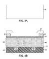
- FIGS. 3A-3Bare pictorial representations (through a top-down and cross sectional view, respectively) illustrating the structure of FIGS. 2A-2B after applying a first block copolymer on the structure.
- FIGS. 4A-4Bare pictorial representations (through a top-down and cross sectional view, respectively) illustrating the structure of FIGS. 3A-3B after annealing the first block copolymer forming an ordered pattern containing repeating structural units within the patterned hard mask.
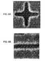
- FIGS. 5A-5Bare scanning electron micrographic (SEM) images of a pattern formed by annealing a block copolymer in accordance with one aspect of the present invention.
- FIGS. 6A-6Bare SEM images illustrating an array of component B polymer blocks of an A-B block copolymer inside a pre-patterned hard mask.
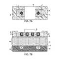
- FIGS. 7A-7Bare pictorial representations (through a top-down and cross sectional view, respectively) illustrating the structure of FIGS. 4A-4B after applying a patterned mask on some of the component B blocks of an annealed A-B block copolymer.
- FIGS. 8A-8Bare pictorial representations (through a top-down and cross sectional view, respectively) illustrating the structure of FIGS. 7A-7B after selectively removing the exposed component B blocks relative to the component A blocks of an annealed A-B block copolymer forming sub-lithographic via openings in the block copolymer.
- FIGS. 9A-9Bare pictorial representations (through a top-down and cross sectional view, respectively) illustrating the structure of FIGS. 8A-8B after transferring the sub-lithographic via openings into the dielectric material.
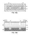
- FIGS. 10A-10Bare pictorial representations (through a top-down and cross sectional view, respectively) illustrating the structure of FIGS. 9A-9B after removing the remaining block copolymer from said structure.
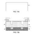
- FIGS. 11A-11Bare pictorial representations (through a top-down and cross sectional view, respectively) illustrating the structure of FIGS. 10A-10B after applying a second block copolymer to said structure.
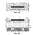
- FIGS. 12A-12Bare pictorial representations (through a top-down and cross sectional view, respectively) illustrating the structure of FIGS. 11A-11B after annealing the second block copolymer forming a second ordered pattern containing repeating structural units within the patterned hard mask.
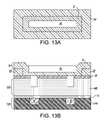
- FIGS. 13A-13Bare pictorial representations (through a top-down and cross sectional view, respectively) illustrating the structure of FIGS. 12A-12B after selectively removing the component B blocks relative to the component A blocks of the second annealed A-B block copolymer forming sub-lithographic line openings in the second block copolymer.
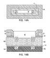
- FIGS. 14A-14Bare pictorial representations (through a top-down and cross sectional view, respectively) illustrating the structure of FIGS. 13A-13B after transferring the sub-lithographic line openings into the dielectric material.
- FIGS. 15A-15Bare pictorial representations (through a top-down and cross sectional view, respectively) illustrating the structure of FIGS. 14A-14B after removing the remaining second block copolymer from said structure.
- FIGS. 16A-16Bare pictorial representations (through a top-down and cross sectional view, respectively) illustrating the structure of FIGS. 15A-15B after removing the patterned hard mask from said structure.
- FIGS. 17A-17Bare pictorial representations (through a top-down and cross sectional view, respectively) illustrating the structure of FIGS. 16A-16B after extending both the sub-lithographic via and line openings into said dielectric material.
- FIGS. 18A-18Bare pictorial representations (through a top-down and cross sectional view, respectively) illustrating the structure of FIGS. 17A-17B after filling said extended sub-lithographic line and via openings with a conductive material.
- the present inventionwhich provides an interconnect structure including nano-scale, e.g., sub-lithographic, lines and vias and a method of fabricating the same, will now be described in greater detail by referring to the following description and drawings that accompany the present application. It is noted that the drawings of the present invention are provided for illustrative purposes and, as such, they are not drawn to scale.
- the present inventionprovides a method to form interconnect structures including nano-scale, e.g., sub-lithographic, lines and vias for future generation of semiconductor technology using self-assembly block copolymers that can be placed at a specific location using a pre-fabricated hard mask pattern.
- Thisprovides an interconnect structure in which the line is self-aligned to the via.
- the method of the present inventionbegins by first providing the structure 10 shown in FIGS. 1A (top down view) and 1 B (cross sectional view).
- the structure 10includes a first interconnect level 12 A which includes a first dielectric material 14 A having at least one conductive feature 16 formed therein and a second interconnect level 12 B which includes a second dielectric material 14 B which are separated by a dielectric cap 15 .
- the structure 10also includes a material stack 18 comprising an etch stop layer 20 located on an upper surface of the second dielectric material 14 B and a hard mask 22 located on an upper surface of the etch stop layer 20 .
- a patterned photoresist 24having at least one lithographically defined opening 26 is shown atop the hard mask 22 .
- the structure 10 shown in FIGS. 1A and 1Bis formed utilizing standard interconnect processing which is well known to those skilled in the art.
- the structure 10can be formed by applying the first dielectric material 14 A to a surface of a substrate (not shown).
- the substratewhich is not shown, may comprise a semiconducting material, an insulating material, a conductive material or any combination thereof.
- the first dielectric material 14 A of the lower interconnect level 12 Amay comprise any interlevel or intralevel dielectric including inorganic dielectrics or organic dielectrics.
- the first dielectric material 14 Amay be porous or non-porous.
- suitable dielectricsthat can be used as the first dielectric material 14 A include, but are not limited to: SiO 2 , silsesquioxanes, C doped oxides (i.e., organosilicates) that include atoms of Si, C, O and H, thermosetting polyarylene ethers, or multilayers thereof
- polyaryleneis used in this application to denote aryl moieties or inertly substituted aryl moieties which are linked together by bonds, fused rings, or inert linking groups such as, for example, oxygen, sulfur, sulfone, sulfoxide, carbonyl and the like.
- the first dielectric material 14 Atypically has a dielectric constant that is about 4.0 or less, with a dielectric constant of about 2.8 or less being even more typical. These dielectrics generally have a lower parasitic crosstalk as compared with dielectric materials that have a higher dielectric constant than 4.0.
- the thickness of the first dielectric material 14 Amay vary depending upon the dielectric material used as well as the exact number of dielectrics within the lower interconnect level 12 A. Typically, and for normal interconnect structures, the first dielectric material 14 A has a thickness from about 200 to about 450 nm.
- the lower interconnect level 12 Aalso has at least one conductive feature 16 that is embedded in (i.e., located within) the first dielectric material 14 A.
- the conductive feature 16is separated from the first dielectric material 14 A by a barrier layer (not specifically shown).
- the conductive feature 16is formed by lithography (i.e., applying a photoresist to the surface of the first dielectric material 14 A, exposing the photoresist to a desired pattern of radiation, and developing the exposed resist utilizing a conventional resist developer), etching (dry etching or wet etching) an opening in the first dielectric material 14 A and filling the etched region with the barrier layer and then with a conductive material forming the conductive feature 16 .
- the barrier layerwhich may comprise Ta, TaN, Ti, TiN, Ru, RuN, W, WN or any other material that can serve as a barrier to prevent conductive material from diffusing there through, is formed by a deposition process such as, for example, atomic layer deposition (ALD), chemical vapor deposition (CVD), plasma enhanced chemical vapor deposition (PECVD), physical vapor deposition (PVD), sputtering, chemical solution deposition, or plating.
- ALDatomic layer deposition
- CVDchemical vapor deposition
- PECVDplasma enhanced chemical vapor deposition
- PVDphysical vapor deposition
- sputteringchemical solution deposition, or plating.
- the thickness of the barrier layermay vary depending on the exact means of the deposition process as well as the material employed.
- the barrier layerhas a thickness from about 4 to about 40 nm, with a thickness from about 7 to about 20 nm being more typical.
- the conductive material used in forming the conductive feature 16includes, for example, polySi, a conductive metal, an alloy comprising at least one conductive metal, a conductive metal silicide or combinations thereof.
- the conductive material that is used in forming the conductive feature 16is a conductive metal such as Cu, W or Al, with Cu or a Cu alloy (such as AlCu) being highly preferred in the present invention.
- the conductive materialis filled into the remaining opening in the first dielectric material 14 A utilizing a conventional deposition process including, but not limited to: CVD, PECVD, sputtering, chemical solution deposition or plating.
- a conventional planarization processsuch as, for example, chemical mechanical polishing (CMP) can be used to provide a structure in which the barrier layer and the conductive feature 16 each have an upper surface that is substantially coplanar with the upper surface of the first dielectric material 14 A.
- CMPchemical mechanical polishing
- the dielectric cap 15is formed on an upper surface of the lower interconnect level 12 A utilizing a conventional deposition process such as, for example, CVD, PECVD, chemical solution deposition, or evaporation.
- the dielectric cap 15comprises any suitable dielectric capping material such as, for example, SiC, Si 4 NH 3 , SiO 2 , a carbon doped oxide, a nitrogen and hydrogen doped silicon carbide SiC(N,H) or multilayers thereof
- the thickness of the dielectric cap 15may vary depending on the technique used to form the same as well as the material make-up of the layer. Typically, the dielectric cap 15 has a thickness from about 15 to about 55 nm, with a thickness from about 25 to about 45 nm being more typical.
- the upper interconnect level 12 Bis formed by applying the second dielectric material 14 B to the upper exposed surface of the dielectric cap 15 .
- the second dielectric material 14 Bmay comprise the same or different, preferably the same, dielectric material as that of the first dielectric material 14 A of the lower interconnect level 12 A.
- the processing techniques and thickness ranges for the first dielectric material 14 Aare also applicable here for the second dielectric material 14 B.
- the material stack 18is then formed on an upper surface of the second dielectric material 14 B.
- the material stack 18comprises an etch stop layer 20 , typically an oxide such as silicon dioxide, and a hard mask 22 , typically a nitride such as silicon nitride.
- the material stack 18is formed utilizing conventional techniques well known to those skilled in the art. For example, a thermal oxidation process can be used in forming the etch stop layer 20 , while a thermal nitridation process can be used in forming the hard mask 22 .
- the etch stop layer 20 and the hard mask 22can each be formed by a conventional deposition process such as, for example, CVD or PECVD. Even further, the etch stop layer 20 and the hard mask 22 may be formed utilizing a combination of thermal and deposition techniques.
- a blanket layer of photoresist material(organic, inorganic or hybrid-type) is then formed atop the upper surface of the material stack 18 .
- the blanket layer of photoresist materialis formed by a conventional deposition process such as, for example, CVD, PECVD, evaporation, or spin-on coating.
- the photoresist materialis subjected to lithography to form patterned photoresist 24 having at least one opening 26 which exposes an upper surface of the hard mask 22 .
- the lithographic stepincludes exposing the photoresist material to radiation and developing the exposed resist utilizing a conventional resist developer.
- the width of the “lithographically defined” opening 26is typically from about 60 to about 120 nm.
- FIGS. 2A (top-down view) and 2 B (cross sectional view)illustrate the structure 10 after transferring the pattern from the patterned photoresist 24 to the hard mask 22 , stopping on the upper surface of the etch stop layer 20 , and stripping of the patterned photoresist 24 .
- reference numeral 26 ′denotes the lithographically defined mask opening in the now patterned hard mask 22 ′ which exposes the upper surface of the etch stop layer 20 .
- the lithographically defined mask opening 26 ′has a width (W) that is limited by the minimum printing critical dimension (CD) of conventional lithography and cannot be further reduced by lithography. It is further noted that the lithographically defined mask opening 26 ′ has a width from about 60 to about 120 nm.
- an etching stepthat selectively removes the exposed portions of the hard mask 22 , not protected by the patterned photoresist 24 , is employed to transfer the pattern to the hard mask 22 .
- the etching steptypically comprises a reactive-ion etching (RIE) in which CHF 3 , CH 2 F 2 , CH 3 F, O 2 and other etchants are used as the etchant.
- RIEreactive-ion etching
- the width (W) of the lithographically defined mask opening 26 ′ in hard mask 22is limited by the minimum printing critical dimension (CD) of conventional lithography and cannot be further reduced using the conventional lithographic techniques alone.
- the present inventiontherefore employs self-assembling block copolymers to form sub-lithographic features (line and via openings) in the lithographically defined mask opening 26 ′.
- each self-assembling block copolymer systemtypically contains two or more different polymeric block components that are immiscible with one another. Under suitable conditions, the two or more immiscible polymeric block components separate into two or more different phases on a nanometer scale and thereby form ordered patterns of isolated nano-sized structural units.
- Such ordered patterns of isolated nano-sized structural units formed by the self-assembling block copolymerscan be used for fabricating nano-scale structural units in semiconductor, optical, and magnetic devices. Specifically, dimensions of the structural units so formed are typically in the range of 10 to 40 nm, which are sub-lithographic (i.e., below the resolutions of the lithographic tools). Further, the self-assembling block copolymers are compatible with conventional semiconductor, optical, and magnetic processes. Therefore, the ordered patterns of nano-sized structural units formed by such block copolymers have been integrated into semiconductor, optical, and magnetic devices where a large, ordered array of repeating structural units are required.
- CMOS technologyrequires precise placement or registration of individual structural units for formation of metal lines and vias in the wiring levels. Therefore, the large, ordered array of repeating structural units formed by self-assembling block copolymers could not be used in CMOS devices, because of lack of alignment or registration of the position of individual structure unit.
- the present inventionprovides a method that combines a conventional lithographic technology with the self-assembling block copolymer technology to form sub-lithographic features in interconnect structure as described above.
- a thin layer of a first self-assembling block copolymer(having a thickness typically ranging from about 20 nm to about 100 nm) is first applied over the structure shown in FIGS. 2A-2B and then annealed to form an ordered pattern containing repeating structural units inside the already formed lithographically defined mask opening 26 ′.
- FIGS. 3A-3Bshow the structure after applying the thin self-assembly block copolymer 28 to the structure shown in FIGS. 2A-2B
- FIGS. 4A-4Bshow the structure after annealing which forms an annealed block copolymer 28 ′.
- the width (W) of the lithographically defined mask opening 26 ′is carefully adjusted so that only a single unit polymer block can be formed therein from the self-assembling block copolymer.
- the single unit polymer blockis embedded in a polymeric matrix that is in turn located inside the lithographically defined mask opening 26 ′, and it has a width that is less than the diameter of the lithographically defined mask opening 26 ′.
- the single unit polymer blockcan be selectively removed relative to the polymeric matrix, thereby leaving a single opening of the smaller width in the polymeric matrix inside the lithographically defined mask opening 26 ′.
- the single opening of the smaller widthcan then be used for sub-lithographic patterning of the dielectric material 14 B.
- block copolymersthere are many different types of block copolymers that can be used for practicing the present invention. As long as a block copolymer contains two or more different polymeric block components that are not immiscible with one another, such two or more different polymeric block components are capable of separating into two or more different phases on a nanometer scale and thereby form patterns of isolated nano-sized structural units under suitable conditions.
- the block copolymerconsists essentially of first and second polymeric block components A and B that are immiscible with each other.
- the block copolymermay contain any numbers of the polymeric block components A and B arranged in any manner.
- the block copolymercan have either a linear or a branched structure.
- such a block polymeris a linear diblock copolymer having the formula of A-B.
- suitable block copolymersmay include, but are not limited to: polystyrene-block-polymethylmethacrylate (PS-b-PMMA), polystyrene-block-polyisoprene (PS-b-PI), polystyrene-block-polybutadiene (PS-b-PBD), polystyrene-block-polyvinylpyridine (PS-b-PVP), polystyrene-block-polyethyleneoxide (PS-b-PEO), polystyrene-block-polyethylene (PS-b-PE), polystyrene-b-polyorganosilicate (PS-b-POS), polystyrene-block-polyferrocenyldimethylsilane (PS-b-PFS), polyethyleneoxide-block-polyisoprene (PEO-b-PI), polyethyleneoxide-block-polybutadiene
- PS-b-PMMApolystyrene-block
- the specific structural units formed by the block copolymerare determined by the molecular weight ratio between the first and second polymeric block components A and B. For example, when the ratio of the molecular weight of the first polymeric block component A over the molecular weight of the second polymeric block component B is greater than about 80:20, the block copolymer will form an ordered array of spheres composed of the second polymeric block component B in a matrix composed of the first polymeric block component A.
- the block copolymerWhen the ratio of the molecular weight of the first polymeric block component A over the molecular weight of the second polymeric block component B is less than about 80:20 but greater than about 60:40, the block copolymer will form an ordered array of cylinders composed of the second polymeric block component B in a matrix composed of the first polymeric block component A. When the ratio of the molecular weight of the first polymeric block component A over the molecular weight of the second polymeric block component B is less than about 60:40 but is greater than about 40:60, the block copolymer will form alternating lamellae composed of the first and second polymeric block components A and B. Therefore, the molecular weight ratio between the first and second polymeric block components A and B can be readily adjusted in the block copolymer of the present invention, in order to form desired structural units.
- the ratio of the molecular weight of the first polymeric block component A over the molecular weight of the second polymeric block component Branges from about 60:40 to about 80:20, so that the block copolymer of the present invention will form alternating layers of the first polymeric block component A and the second polymeric block component B.
- one of the components A and Bcan be selectively removable relative to the other, thereby resulting in either orderly arranged structural units composed of the un-removed component.
- the second polymeric block component Bis selectively removable relative to the first polymeric block component A, orderly arranged trenches can be formed.
- the block copolymer used for forming the self-assembled periodic patterns of the present inventionis PS-b-PMMA with a PS:PMMA molecular weight ratio ranging from about 20:80 to about 80:20.
- ⁇ Nthe degree of polymerization.
- ⁇ Nthe higher the repulsion between the different blocks in the block copolymer, and the more likely the phase separation therebetween.
- ⁇ N>10which is hereinafter referred to as the strong segregation limit
- ⁇can be calculated as approximately 0.028+3.9/T, where T is the absolute temperature. Therefore, ⁇ is approximately 0.0362 at 473K ( ⁇ 200° C.).
- M nmolecular weight of the PS-b-PMMA diblock copolymer
- PS:PMMAmolecular weight ratio
- the mutual compulsion between the different polymeric block components in the block copolymer of the present inventioncan be readily controlled to effectuate desired phase separation between the different block components.
- the phase separationin turn leads to formation of self-assembled periodic patterns containing ordered arrays of repeating structural units (i.e., spheres, cylinders, or lamellae), as described hereinabove.
- the block copolymeris first dissolved in a suitable solvent system to form a block copolymer solution, which is then applied onto a surface to form a thin block copolymer layer, followed by annealing of the thin block copolymer layer, thereby effectuating phase separation between different polymeric block components contained in the block copolymer.
- the solvent system used for dissolving the block copolymer and forming the block copolymer solutionmay comprise any suitable solvent, including, but not limited to: toluene, propylene glycol monomethyl ether acetate (PGMEA), propylene glycol monomethyl ether (PGME), and acetone.
- the block copolymer solutionpreferably contains the block copolymer at a concentration ranging from about 0.1% to about 2% by total weight of the solution. More preferably, the block copolymer solution contains the block copolymer at a concentration ranging from about 0.5 wt % to about 1.5 wt %.
- the block copolymer solutioncan be applied to the surface of an interconnect structure by any suitable techniques, including, but not limited to: spin casting, coating, spraying, ink coating, dip coating, etc.
- the block copolymer solutionis spin cast onto the surface of an interconnect structure to form a thin block copolymer layer thereon.
- the entire device structureis annealed to effectuate micro-phase segregation of the different block components contained by the block copolymer, thereby forming the periodic patterns with repeating structural units.
- Annealing of the block copolymer in the present inventioncan be achieved by various methods known in the art, including, but not limited to: thermal annealing (either in a vacuum or in an inert atmosphere containing nitrogen or argon), ultra-violet annealing, laser annealing, solvent vapor-assisted annealing (either at or above room temperature), and supercritical fluid-assisted annealing, which are not described in detail here in order to avoid obscuring the invention.
- a thermal annealing stepis carried out to anneal the block copolymer layer at an elevated annealing temperature that is above the glass transition temperature (T g ) of the block copolymer, but below the decomposition or degradation temperature (T d ) of the block copolymer. More preferably, the thermal annealing step is carried out an annealing temperature of about 200° C.-300° C. The thermal annealing may last from less than about 1 hour to about 100 hours, and more typically from about 1 hour to about 15 hours.
- the block copolymer layeris annealed by ultra-violet (UV) treatment.
- UVultra-violet
- the annealed block copolymer 28 ′can comprise first and second polymeric components A and B, in which the pattern is an ordered array of cylinders composed of the block component B in a polymeric matrix composed of the polymeric block component A.
- Such an annealed block copolymer in which the ordered array of cylinders is aligned vertical with a surface of the second dielectric material 14 Bis shown in FIGS. 4A-4B .
- the B blockscan be used to provide sub-lithographic via openings having a width from about 10 to about 40 nm into the second dielectric material 14 B. This is achieved by having the cylindrical shaped block aligned vertical to the surface of the second dielectric material 14 B.
- the cylindrical shaped blockis aligned parallel to the surface of the second dielectric material 14 B.
- the particular alignment of the cylindrical blockis determined by the surface wetting conditions as are described in greater detail below.
- FIG. 5Ais a top-down scanning electron microscopic (SEM) photographs of a pattern formed by an annealed block copolymer film that comprises first and second block copolymer components A and B, where the patterned contains an order array of vertically arranged cylinders composed of the polymeric block component B in a polymeric matrix composed of the polymeric block component A.
- SEMsscanning electron microscopic
- the dark spotsrepresent the B component.
- a hard mask layeris deposited and etched with an array of via patterns prior to the application of the block copolymer. Each dark spot (component B of an A-B copolymer) is located at the center of each via shaped hard mask opening.
- FIG. 5Bis a top-down SEM illustrating the details of component B polymer pattern inside the via-shaped hard mask as well as dimensions of the ordered array of cylinders shown in FIG. 5A .
- FIGS. 6A-6Bare top-down SEMs illustrating an array of component B polymer blocks inside the pre-patterned hard mask.
- the present inventionemploys lithographic features to limit formation and placement of the structural units formed by the self-assembling block copolymer materials. More specifically, the lithographic features as used by the present invention have dimensions that are adjusted so that only a single unit polymer block can be formed and placed inside each lithographic feature from the self-assembling block copolymer.
- the interior surfaces of the lithographically defined mask opening 26 ′are treated before application of a block copolymer layer.
- one or more surface layersare formed over the bottom surface and sidewall surfaces of the lithographically defined mask opening 26 ′, so as to provide the desired wetting properties for aligning the alternating layers of unit polymeric blocks to be formed with the lithographically defined mask opening 26 ′.
- the wetting properties as discussed hereinrefer to the surface affinities of a specific surface with respect to the different block components of the block copolymers. For example, if a surface has substantially the same surface affinity to both block components A and B of a block copolymer, such a surface is considered a neutral surface or a non-preferential surface, i.e., both block components A and B can wet or have affinities to such a surface. In contrast, if a surface has significantly different surface affinities for the block components A and B, such a surface is then considered a preferential surface, i.e., only one of block components A and B can wet such a surface, but the other cannot.
- alternating layers of polymeric blocks that are aligned perpendicular to the bottom surface of the lithographically defined mask opening 26 ′ from PS-b-PMMAit is desired to deposit a neutral or non-preferential monolayer (e.g., a substantially homogenous mixture of PS and PMMA components) over the bottom surface of the lithographically defined mask opening 26 ′, while the sidewall surfaces of the lithographically defined mask opening 26 ′ are either left untreated or are coated with a preferential wetting material (e.g., silicon native oxides, silicon oxides, and silicon nitrides).
- a preferential wetting materiale.g., silicon native oxides, silicon oxides, and silicon nitrides
- FIGS. 7A-7Billustrates the next processing steps of the present invention which are preformed after annealing the block copolymer 28 .
- FIGS. 7A-7Bshows the structure after a patterned photoresist mask 30 is formed atop portions of the annealed block copolymer 28 ′ so as to protect some portions of the annealed block copolymer 28 ′, particularly some of the vertically aligned cylinders B, that are not to be etched.
- the patterned mask 30is formed by conventional processes well known in the art, e.g., deposition and lithography.
- FIGS. 8A-8Bshow the structure after etching the exposed second polymeric block copolymer component B therefrom.
- the resultant structurenow includes sub-lithographic via openings 32 having a width from about 10 to about 40 nm in the annealed block copolymer 28 ′.
- the sub-lithographic via openings 32are formed by selectively etching (via a dry etching or wetting etching process) the exposed second polymeric block copolymer component B relative to the first polymeric block copolymer component A utilizing patterned mask 30 as an etch mask.
- FIGS. 9A-9Bshow the structure after extending the sub-lithographic via openings 32 through portions of the underlying etch stop layer 20 and second dielectric material 14 B.
- the extending of the sub-lithographic via openings 32is performed utilizing an etching process such as, for example, reactive-ion etching.
- FIGS. 10A-10Billustrate the structure after the patterned mask 30 and the remaining portions of the annealed block copolymer 28 ′ have been removed.
- a single polymer stripping step, or multiple polymer stripping steps,can be employed in the present invention.
- a second thin self-assembly block copolymer layer 34is applied to the structure as is shown in FIGS. 11A-11B .
- the second block copolymer 34may comprise the same or different block copolymer, the only difference being that the surface wetting conditions are chosen such that the ordered array of cylindrical blocks of the annealed block copolymer is aligned in a different direction than that of the first.
- the second block copolymerhas wetting conditions such that the ordered array of cylindrical blocks of the annealed polymer is aligned parallel with the surface of the interconnect structure thus allowing for forming a sub-lithographic line opening patterns having a width from about 10 to about 40 nm.
- FIGS. 12A-12Billustrate the structure after the second block copolymer has been annealed (using the conditions described above) to form an annealed block copolymer 34 ′ comprising first and second polymeric components A′ and B′, in which the pattern is an ordered array of cylinders composed of the block component B′ in a polymeric matrix composed of the polymeric block component A′.
- the B block copolymeris aligned parallel with the surface of the interconnect structure.
- FIGS. 13A-13Billustrate the structure after removing the ordered array of cylinders composed of the block component B′ that are aligned parallel to the surface of the substrate selective to block component A′. This removal process is performed utilizing a selective etching process including dry etching or wet etching. It is noted that in FIGS. 13A-13B , reference numeral 36 represents a sub-lithographic line opening having a width from about 10 to about 40 nm.
- FIGS. 14A-14Billustrate the structure after extending the sub-lithographic line opening 36 into the underlying portions of the etch stop layer 20 and the second dielectric material 14 B.
- a reactive-ion etching processis typically used to extend the sub-lithographic line opening into the structure.
- FIGS. 15A-15Billustrate the structure after removing the block component A′ utilizing a conventional stripping process that selectively removes a polymeric material relative to a dielectric material.
- FIGS. 16A-16Billustrate the structure after a planarizing step (such as chemical mechanical polishing) has been performed which removes the remaining patterned hard mask 22 ′ from the structure exposing the upper surface of the etch stop layer 20 .
- a planarizing stepsuch as chemical mechanical polishing
- FIGS. 17A-17Billustrate the structure after an etching process such as reactive-ion etching (RIE) is performed which extends both the sub-lithographic line opening 36 and the sub-lithographic via opening 32 into the second dielectric material 14 B. Since the sub-lithographic via opening 32 has a smaller width than the sub-lithographic line opening 36 , it etches at a faster rate than the line opening 36 .
- RIEreactive-ion etching
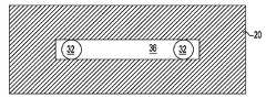
- FIGS. 18A-18Billustrate the structure after conductive material 38 has been formed into the sub-lithographic via and line openings.
- the conductive material 38 used in filling the sub-lithographically defined openingsincludes, for example, polySi, a conductive metal, an alloy comprising at least one conductive metal, a conductive metal silicide or combinations thereof.
- the conductive material 38is a conductive metal such as Cu, W or Al, with Cu or a Cu alloy (such as AlCu) being highly preferred in the present invention.
- the conductive material 38is filled into the sub-lithographically defined via and line openings utilizing a conventional deposition process including, but not limited to: CVD, PECVD, sputtering, chemical solution deposition or plating.
- a conventional planarization processsuch as, for example, chemical mechanical polishing (CMP) can be used to provide a planarized structure as is shown in FIGS. 18-18B . It is emphasized that the sub-lithographic conductively filled line is self-aligned to that of the underlining sub-lithographically filled via.
- CMPchemical mechanical polishing
Landscapes
- Engineering & Computer Science (AREA)
- Physics & Mathematics (AREA)
- Condensed Matter Physics & Semiconductors (AREA)
- General Physics & Mathematics (AREA)
- Microelectronics & Electronic Packaging (AREA)
- Manufacturing & Machinery (AREA)
- Computer Hardware Design (AREA)
- Power Engineering (AREA)
- Chemical & Material Sciences (AREA)
- Inorganic Chemistry (AREA)
- Nanotechnology (AREA)
- Analytical Chemistry (AREA)
- Composite Materials (AREA)
- Materials Engineering (AREA)
- Crystallography & Structural Chemistry (AREA)
- Internal Circuitry In Semiconductor Integrated Circuit Devices (AREA)
Abstract
Description
- The present invention relates to a semiconductor structure and a method of fabricating the same. More particularly, the present invention relates to an interconnect structure including nano-scale conductively filled openings and a method of fabricating the same.
- Generally, semiconductor devices include a plurality of circuits which form an integrated circuit fabricated on a semiconductor substrate. A complex network of signal paths will normally be routed to connect the circuit elements distributed on the surface of the substrate. Efficient routing of these signals across the device requires formation of multilayered schemes. These interconnect structures typically include copper, Cu, since Cu based interconnects provide higher speed signal transmission between large numbers of transistors on a complex semiconductor chip as compared to aluminum-based interconnects.
- Within a typical interconnect structure, metal vias run perpendicular to the semiconductor substrate and metal lines run parallel to the semiconductor substrate. Further enhancement of the signal speed and reduction of signals in adjacent metal lines are achieved in today's integrated circuit product chips by embedding the metal lines and vias in a dielectric material having a dielectric constant of less than silicon dioxide.
- In the prior art, interconnect structures are typically fabricated utilizing lithography and etching to define the dimensions of the lines and vias. Photoresists and hard masks are typically used as a means to transfer a desired line and/or via pattern into an underlying dielectric material. As such, the dimensions of the line and/or via openings are limited to the resolution of the lithographic tool. Typically, the currently available 0.93 numerical aperture (NA) lithographic tool can only resolve lithographic patterns with openings of not less than 100 nm in diameter. Future generation of 1.2 NA lithographic tools are expected to print lithographic patterns with openings of about 70 to about 80 nm. Such large opening diameters contribute to undesirable low device density of the integrated circuit.
- Moreover, as semiconductor device technology scales, interconnect wiring needs to scale accordingly. The current 45 nm node technology requires the M1-M4 (i.e., the first-fourth metal interconnect) lines to be 64 nm, and upcoming 32 nm node technology requires the same metal lines to be 45 nm, which is beyond the conventional lithographic capabilities as mentioned above.
- Therefore, there is a need for reducing the diameters of the openings of the interconnect wiring structures to below the resolutions of the lithographic tools, i.e., there is a need for sub-lithographic feature patterning of interconnect structures for the 64 nm and 32 nm node generations.
- The present invention provides a method to form interconnect structures including nano-scale, e.g., sub-lithographic, lines and vias for future generation of semiconductor technology using self-assembly block copolymers that can be placed at a specific location using a pre-fabricated hard mask pattern. The inventive method provides an interconnect structure in which the line is self-aligned to the via. It is noted that the terms “nano-scale” and “sub-lithographic” are used interchangeably throughout the instant application to denote patterns or openings whose widths are below 60 nm.
- In general terms, the present invention provides a method for forming an interconnect structure which comprises:
- providing a structure including a patterned hard mask having a lithographically defined opening located above a dielectric material;
- forming at least one self-assembling block copolymer having a first polymeric component and a second polymeric component embedded within said at least one lithographically defined opening;
- selectively removing one of said first or second polymeric components relative to the other component to form sub-lithographic openings in said at least one self-assembling block copolymer;
- transferring said sub-lithographic openings into said dielectric material; and
- filling said sub-lithographic openings with a conductive material.
- In one aspect of the present invention, sub-lithographic lines and vias are formed by utilizing self-assembly block copolymers that have different wetting conditions. In such an aspect, the self-aligned block copolymers form an ordered array of cylinders that, depending on the surface wetting conditions, may be aligned vertical with a surface of the dielectric material or aligned parallel to the surface of the dielectric material. The vertical alignment of the ordered array of cylinders is used in forming sub-lithographic vias, while the parallel alignment of the ordered array of cylinders is used in forming sub-lithographic lines.
- More specifically, the method of the present invention comprises:
- providing a structure including a patterned hard mask located above a dielectric material, wherein said patterned hard mask includes at least one lithographically defined opening;
- providing a first block copolymer having a first single unit polymer block with a sub-lithographic width inside the at least one lithographically defined opening, wherein the first single unit polymer block comprises a second polymeric block component which is embedded in a polymeric matrix that comprises a first polymeric block component of said first block copolymer;
- selectively removing the second polymeric block component relative to the first polymeric block component to form a first sub-lithographic opening in the polymeric matrix inside the at least one lithographically defined opening;
- patterning the dielectric material using the first sub-lithographic opening;
- providing a second block copolymer having a second single unit polymer block with a sub-lithographic width inside the at least one lithographically defined opening, wherein the second single unit polymer block comprises a second polymeric block component which is embedded in a polymeric matrix that comprises a first polymeric block component of said second block copolymer;
- selectively removing the second polymeric block component of said second block copolymer relative to the first polymeric block of said second block copolymer to form a second sub-lithographic opening in the polymeric matrix inside the at least one lithographically defined opening;
- transferring said second sub-lithographic opening to said dielectric material; and
- filling the first and second sub-lithographic openings with a conductive material.
- In one highly preferred embodiment of the present invention, the first sub-lithographic opening is a sub-lithographic via opening having a width from about 10 to about 40 nm, while the second sub-lithographic opening is a sub-lithographic line opening having a width from about 10 to about 40 nm. In yet another embodiment, which is less preferred relative to the one mentioned above, the first sub-lithographic opening is a sub-lithographic line opening having a width from about 10 to about 40 nm, while the second sub-lithographic opening is a sub-lithographic via opening having a width from about 10 to about 40 nm.
- The block copolymers as mentioned hereinabove preferably comprise A:B block copolymers wherein A is a first polymeric component and B is a second polymeric component having a weight ratio of A:B from about 20:80 to about 80:20, and the single unit polymer block preferably comprises a cylinder that stands vertical or parallel to an upper surface of the dielectric material. The block copolymers can be readily selected from the group consisting of polystyrene-block-polymethylmethacrylate (PS-b-PMMA), polystyrene-block-polyisoprene (PS-b-PI), polystyrene-block-polybutadiene (PS-b-PBD), polystyrene-block-polyvinylpyridine (PS-b-PVP), polystyrene-block-polyethyleneoxide (PS-b-PEO), polystyrene-block-polyethylene (PS-b-PE), polystyrene-b-polyorganosilicate (PS-b-POS), polystyrene-block-polyferrocenyldimethylsilane (PS-b-PFS), polyethyleneoxide-block-polyisoprene (PEO-b-PI), polyethyleneoxide-block-polybutadiene (PEO-b-PBD), polyethyleneoxide-block-polymethylmethacrylate (PEO-b-PMMA), polyethyleneoxide-block-polyethylethylene (PEO-b-PEE), polybutadiene-block-polyvinylpyridine (PBD-b-PVP), and polyisoprene-block-polymethylmethacrylate (PI-b-PMMA). In a particularly preferred, but not necessary, embodiment of the present invention, the block copolymers comprise PS-b-PMMA having a PS:PMMA weight ratio ranging from about 20:80 to about 80:20.
- In another aspect of the present invention, an interconnect structure having sub-lithographic conductively filled lines and vias embedded with a dielectric material is provided. Specifically, the inventive structure comprises:
- a dielectric material having at least one conductively filled via having a width from about 10 to about 40 nm, and at least one conductively filled line having a width from about 10 to about 40 nm embedded therein, wherein said at least one conductively filled line is self-aligned to the at least one conductively filled via.
- The term “self-aligned” is used in the present application to denote that the via and line openings are formed using one lithographically defined hard mask and the alignment error between the via and line openings is smaller than that between two lithographic masks.
- Other aspects, features and advantages of the invention will be more fully apparent from the ensuing disclosure and appended claims.
FIGS. 1A-1B are pictorial representations (through a top-down and cross sectional view, respectively) illustrating an initial interconnect structure with a patterned photoresist having at least one lithographically defined opening located atop a hark mask that is disposed above a dielectric material.FIGS. 2A-2B are pictorial representations (through a top-down and cross sectional view, respectively) illustrating the structure ofFIGS. 1A-1B after transferring the lithographic defined opening into the hard mask.FIGS. 3A-3B are pictorial representations (through a top-down and cross sectional view, respectively) illustrating the structure ofFIGS. 2A-2B after applying a first block copolymer on the structure.FIGS. 4A-4B are pictorial representations (through a top-down and cross sectional view, respectively) illustrating the structure ofFIGS. 3A-3B after annealing the first block copolymer forming an ordered pattern containing repeating structural units within the patterned hard mask.FIGS. 5A-5B are scanning electron micrographic (SEM) images of a pattern formed by annealing a block copolymer in accordance with one aspect of the present invention.FIGS. 6A-6B are SEM images illustrating an array of component B polymer blocks of an A-B block copolymer inside a pre-patterned hard mask.FIGS. 7A-7B are pictorial representations (through a top-down and cross sectional view, respectively) illustrating the structure ofFIGS. 4A-4B after applying a patterned mask on some of the component B blocks of an annealed A-B block copolymer.FIGS. 8A-8B are pictorial representations (through a top-down and cross sectional view, respectively) illustrating the structure ofFIGS. 7A-7B after selectively removing the exposed component B blocks relative to the component A blocks of an annealed A-B block copolymer forming sub-lithographic via openings in the block copolymer.FIGS. 9A-9B are pictorial representations (through a top-down and cross sectional view, respectively) illustrating the structure ofFIGS. 8A-8B after transferring the sub-lithographic via openings into the dielectric material.FIGS. 10A-10B are pictorial representations (through a top-down and cross sectional view, respectively) illustrating the structure ofFIGS. 9A-9B after removing the remaining block copolymer from said structure.FIGS. 11A-11B are pictorial representations (through a top-down and cross sectional view, respectively) illustrating the structure ofFIGS. 10A-10B after applying a second block copolymer to said structure.FIGS. 12A-12B are pictorial representations (through a top-down and cross sectional view, respectively) illustrating the structure ofFIGS. 11A-11B after annealing the second block copolymer forming a second ordered pattern containing repeating structural units within the patterned hard mask.FIGS. 13A-13B are pictorial representations (through a top-down and cross sectional view, respectively) illustrating the structure ofFIGS. 12A-12B after selectively removing the component B blocks relative to the component A blocks of the second annealed A-B block copolymer forming sub-lithographic line openings in the second block copolymer.FIGS. 14A-14B are pictorial representations (through a top-down and cross sectional view, respectively) illustrating the structure ofFIGS. 13A-13B after transferring the sub-lithographic line openings into the dielectric material.FIGS. 15A-15B are pictorial representations (through a top-down and cross sectional view, respectively) illustrating the structure ofFIGS. 14A-14B after removing the remaining second block copolymer from said structure.FIGS. 16A-16B are pictorial representations (through a top-down and cross sectional view, respectively) illustrating the structure ofFIGS. 15A-15B after removing the patterned hard mask from said structure.FIGS. 17A-17B are pictorial representations (through a top-down and cross sectional view, respectively) illustrating the structure ofFIGS. 16A-16B after extending both the sub-lithographic via and line openings into said dielectric material.FIGS. 18A-18B are pictorial representations (through a top-down and cross sectional view, respectively) illustrating the structure ofFIGS. 17A-17B after filling said extended sub-lithographic line and via openings with a conductive material.- The present invention, which provides an interconnect structure including nano-scale, e.g., sub-lithographic, lines and vias and a method of fabricating the same, will now be described in greater detail by referring to the following description and drawings that accompany the present application. It is noted that the drawings of the present invention are provided for illustrative purposes and, as such, they are not drawn to scale.
- In the following description, numerous specific details are set forth, such as particular structures, components, materials, dimensions, processing steps and techniques, in order to provide a thorough understanding of the present invention. However, it will be appreciated by one of ordinary skill in the art that the invention may be practiced without these specific details. In other instances, well-known structures or processing steps have not been described in detail in order to avoid obscuring the invention.
- It will be understood that when an element as a layer, region or substrate is referred to as being “on” or “over” another element, it can be directly on the other element or intervening elements may also be present. In contrast, when an element is referred to as being “directly on” or “directly over” another element, there are no intervening elements present. It will also be understood that when an element is referred to as being “connected” or “coupled” to another element, it can be directly connected or coupled to the other element or intervening elements may be present. In contrast, when an element is referred to as being “directly connected” or “directly coupled” to another element, there are no intervening elements present.
- As stated above, the present invention provides a method to form interconnect structures including nano-scale, e.g., sub-lithographic, lines and vias for future generation of semiconductor technology using self-assembly block copolymers that can be placed at a specific location using a pre-fabricated hard mask pattern. This provides an interconnect structure in which the line is self-aligned to the via.
- The method of the present invention begins by first providing the
structure 10 shown inFIGS. 1A (top down view) and1B (cross sectional view). As is shown in the cross sectional view, thestructure 10 includes afirst interconnect level 12A which includes a firstdielectric material 14A having at least oneconductive feature 16 formed therein and asecond interconnect level 12B which includes a seconddielectric material 14B which are separated by adielectric cap 15. Thestructure 10 also includes amaterial stack 18 comprising anetch stop layer 20 located on an upper surface of the seconddielectric material 14B and ahard mask 22 located on an upper surface of theetch stop layer 20. A patternedphotoresist 24 having at least one lithographically definedopening 26 is shown atop thehard mask 22. - The
structure 10 shown inFIGS. 1A and 1B is formed utilizing standard interconnect processing which is well known to those skilled in the art. For example, thestructure 10 can be formed by applying the firstdielectric material 14A to a surface of a substrate (not shown). The substrate, which is not shown, may comprise a semiconducting material, an insulating material, a conductive material or any combination thereof. - The first
dielectric material 14A of thelower interconnect level 12A may comprise any interlevel or intralevel dielectric including inorganic dielectrics or organic dielectrics. The firstdielectric material 14A may be porous or non-porous. Some examples of suitable dielectrics that can be used as the firstdielectric material 14A include, but are not limited to: SiO2, silsesquioxanes, C doped oxides (i.e., organosilicates) that include atoms of Si, C, O and H, thermosetting polyarylene ethers, or multilayers thereof The term “polyarylene” is used in this application to denote aryl moieties or inertly substituted aryl moieties which are linked together by bonds, fused rings, or inert linking groups such as, for example, oxygen, sulfur, sulfone, sulfoxide, carbonyl and the like. - The first
dielectric material 14A typically has a dielectric constant that is about 4.0 or less, with a dielectric constant of about 2.8 or less being even more typical. These dielectrics generally have a lower parasitic crosstalk as compared with dielectric materials that have a higher dielectric constant than 4.0. The thickness of the firstdielectric material 14A may vary depending upon the dielectric material used as well as the exact number of dielectrics within thelower interconnect level 12A. Typically, and for normal interconnect structures, the firstdielectric material 14A has a thickness from about 200 to about 450 nm. - The
lower interconnect level 12A also has at least oneconductive feature 16 that is embedded in (i.e., located within) the firstdielectric material 14A. Theconductive feature 16 is separated from the firstdielectric material 14A by a barrier layer (not specifically shown). Theconductive feature 16 is formed by lithography (i.e., applying a photoresist to the surface of the firstdielectric material 14A, exposing the photoresist to a desired pattern of radiation, and developing the exposed resist utilizing a conventional resist developer), etching (dry etching or wet etching) an opening in the firstdielectric material 14A and filling the etched region with the barrier layer and then with a conductive material forming theconductive feature 16. - The barrier layer, which may comprise Ta, TaN, Ti, TiN, Ru, RuN, W, WN or any other material that can serve as a barrier to prevent conductive material from diffusing there through, is formed by a deposition process such as, for example, atomic layer deposition (ALD), chemical vapor deposition (CVD), plasma enhanced chemical vapor deposition (PECVD), physical vapor deposition (PVD), sputtering, chemical solution deposition, or plating. The thickness of the barrier layer may vary depending on the exact means of the deposition process as well as the material employed. Typically, the barrier layer has a thickness from about 4 to about 40 nm, with a thickness from about 7 to about 20 nm being more typical.
- Following the barrier layer formation, the remaining region of the opening within the first
dielectric material 14A is filled with a conductive material forming theconductive feature 16. The conductive material used in forming theconductive feature 16 includes, for example, polySi, a conductive metal, an alloy comprising at least one conductive metal, a conductive metal silicide or combinations thereof. Preferably, the conductive material that is used in forming theconductive feature 16 is a conductive metal such as Cu, W or Al, with Cu or a Cu alloy (such as AlCu) being highly preferred in the present invention. The conductive material is filled into the remaining opening in the firstdielectric material 14A utilizing a conventional deposition process including, but not limited to: CVD, PECVD, sputtering, chemical solution deposition or plating. After deposition, a conventional planarization process such as, for example, chemical mechanical polishing (CMP) can be used to provide a structure in which the barrier layer and theconductive feature 16 each have an upper surface that is substantially coplanar with the upper surface of the firstdielectric material 14A. - After forming the at least one
conductive feature 16, thedielectric cap 15 is formed on an upper surface of thelower interconnect level 12A utilizing a conventional deposition process such as, for example, CVD, PECVD, chemical solution deposition, or evaporation. Thedielectric cap 15 comprises any suitable dielectric capping material such as, for example, SiC, Si4NH3, SiO2, a carbon doped oxide, a nitrogen and hydrogen doped silicon carbide SiC(N,H) or multilayers thereof The thickness of thedielectric cap 15 may vary depending on the technique used to form the same as well as the material make-up of the layer. Typically, thedielectric cap 15 has a thickness from about 15 to about 55 nm, with a thickness from about 25 to about 45 nm being more typical. - Next, the
upper interconnect level 12B is formed by applying the seconddielectric material 14B to the upper exposed surface of thedielectric cap 15. The seconddielectric material 14B may comprise the same or different, preferably the same, dielectric material as that of the firstdielectric material 14A of thelower interconnect level 12A. The processing techniques and thickness ranges for the firstdielectric material 14A are also applicable here for the seconddielectric material 14B. - After forming the second
dielectric material 14B, thematerial stack 18 is then formed on an upper surface of the seconddielectric material 14B. In an aspect of the present invention, and as illustrated inFIG. 1B , thematerial stack 18 comprises anetch stop layer 20, typically an oxide such as silicon dioxide, and ahard mask 22, typically a nitride such as silicon nitride. Thematerial stack 18 is formed utilizing conventional techniques well known to those skilled in the art. For example, a thermal oxidation process can be used in forming theetch stop layer 20, while a thermal nitridation process can be used in forming thehard mask 22. Alternatively, theetch stop layer 20 and thehard mask 22 can each be formed by a conventional deposition process such as, for example, CVD or PECVD. Even further, theetch stop layer 20 and thehard mask 22 may be formed utilizing a combination of thermal and deposition techniques. - After forming the
material stack 18, a blanket layer of photoresist material (organic, inorganic or hybrid-type) is then formed atop the upper surface of thematerial stack 18. The blanket layer of photoresist material is formed by a conventional deposition process such as, for example, CVD, PECVD, evaporation, or spin-on coating. Following the application of the blanket layer of photoresist material, the photoresist material is subjected to lithography to form patternedphotoresist 24 having at least oneopening 26 which exposes an upper surface of thehard mask 22. The lithographic step includes exposing the photoresist material to radiation and developing the exposed resist utilizing a conventional resist developer. The width of the “lithographically defined”opening 26 is typically from about 60 to about 120 nm. FIGS. 2A (top-down view) and2B (cross sectional view) illustrate thestructure 10 after transferring the pattern from the patternedphotoresist 24 to thehard mask 22, stopping on the upper surface of theetch stop layer 20, and stripping of the patternedphotoresist 24. InFIG. 2B ,reference numeral 26′ denotes the lithographically defined mask opening in the now patternedhard mask 22′ which exposes the upper surface of theetch stop layer 20. It is noted that the lithographically defined mask opening26′ has a width (W) that is limited by the minimum printing critical dimension (CD) of conventional lithography and cannot be further reduced by lithography. It is further noted that the lithographically defined mask opening26′ has a width from about 60 to about 120 nm.- Next, an etching step that selectively removes the exposed portions of the
hard mask 22, not protected by the patternedphotoresist 24, is employed to transfer the pattern to thehard mask 22. The etching step typically comprises a reactive-ion etching (RIE) in which CHF3, CH2F2, CH3F, O2and other etchants are used as the etchant. After etching and pattern transfer, the patternedphotoresist 24 is stripped from the structure utilizing a conventional resist stripping process. - As stated above, the width (W) of the lithographically defined mask opening26′ in
hard mask 22 is limited by the minimum printing critical dimension (CD) of conventional lithography and cannot be further reduced using the conventional lithographic techniques alone. The present invention therefore employs self-assembling block copolymers to form sub-lithographic features (line and via openings) in the lithographically defined mask opening26′. - It has been known that certain materials are capable of spontaneous organization of materials into ordered patterns without the need for human interference, which is typically referred to as the self-assembly of materials. Examples of material self-assembly range from snowflakes to seashells to sand dunes, all of which form some type of regular or ordered patterns in response to the external conditions.
- Among various self-assembling materials, self-assembling block copolymers that are capable of self-organizing into nanometer-scale patterns are particularly promising for enabling future advances in the semiconductor technology. Each self-assembling block copolymer system typically contains two or more different polymeric block components that are immiscible with one another. Under suitable conditions, the two or more immiscible polymeric block components separate into two or more different phases on a nanometer scale and thereby form ordered patterns of isolated nano-sized structural units.
- Such ordered patterns of isolated nano-sized structural units formed by the self-assembling block copolymers can be used for fabricating nano-scale structural units in semiconductor, optical, and magnetic devices. Specifically, dimensions of the structural units so formed are typically in the range of 10 to 40 nm, which are sub-lithographic (i.e., below the resolutions of the lithographic tools). Further, the self-assembling block copolymers are compatible with conventional semiconductor, optical, and magnetic processes. Therefore, the ordered patterns of nano-sized structural units formed by such block copolymers have been integrated into semiconductor, optical, and magnetic devices where a large, ordered array of repeating structural units are required.
- However, the CMOS technology requires precise placement or registration of individual structural units for formation of metal lines and vias in the wiring levels. Therefore, the large, ordered array of repeating structural units formed by self-assembling block copolymers could not be used in CMOS devices, because of lack of alignment or registration of the position of individual structure unit.
- The present invention provides a method that combines a conventional lithographic technology with the self-assembling block copolymer technology to form sub-lithographic features in interconnect structure as described above.
- Specifically, a thin layer of a first self-assembling block copolymer (having a thickness typically ranging from about 20 nm to about 100 nm) is first applied over the structure shown in
FIGS. 2A-2B and then annealed to form an ordered pattern containing repeating structural units inside the already formed lithographically defined mask opening26′. FIGS. 3A-3B show the structure after applying the thin self-assembly block copolymer 28 to the structure shown inFIGS. 2A-2B , whileFIGS. 4A-4B show the structure after annealing which forms an annealedblock copolymer 28′.- It is noted that the width (W) of the lithographically defined mask opening26′ is carefully adjusted so that only a single unit polymer block can be formed therein from the self-assembling block copolymer. The single unit polymer block is embedded in a polymeric matrix that is in turn located inside the lithographically defined mask opening26′, and it has a width that is less than the diameter of the lithographically defined mask opening26′. The single unit polymer block can be selectively removed relative to the polymeric matrix, thereby leaving a single opening of the smaller width in the polymeric matrix inside the lithographically defined mask opening26′. The single opening of the smaller width can then be used for sub-lithographic patterning of the
dielectric material 14B. - There are many different types of block copolymers that can be used for practicing the present invention. As long as a block copolymer contains two or more different polymeric block components that are not immiscible with one another, such two or more different polymeric block components are capable of separating into two or more different phases on a nanometer scale and thereby form patterns of isolated nano-sized structural units under suitable conditions.
- In a preferred, but not necessary, embodiment of the present invention, the block copolymer consists essentially of first and second polymeric block components A and B that are immiscible with each other. The block copolymer may contain any numbers of the polymeric block components A and B arranged in any manner. The block copolymer can have either a linear or a branched structure. Preferably, such a block polymer is a linear diblock copolymer having the formula of A-B.
- Specific examples of suitable block copolymers that can be used for forming the structural units of the present invention may include, but are not limited to: polystyrene-block-polymethylmethacrylate (PS-b-PMMA), polystyrene-block-polyisoprene (PS-b-PI), polystyrene-block-polybutadiene (PS-b-PBD), polystyrene-block-polyvinylpyridine (PS-b-PVP), polystyrene-block-polyethyleneoxide (PS-b-PEO), polystyrene-block-polyethylene (PS-b-PE), polystyrene-b-polyorganosilicate (PS-b-POS), polystyrene-block-polyferrocenyldimethylsilane (PS-b-PFS), polyethyleneoxide-block-polyisoprene (PEO-b-PI), polyethyleneoxide-block-polybutadiene (PEO-b-PBD), polyethyleneoxide-block-polymethylmethacrylate (PEO-b-PMMA), polyethyleneoxide-block-polyethylethylene (PEO-b-PEE), polybutadiene-block-polyvinylpyridine (PBD-b-PVP), and polyisoprene-block-polymethylmethacrylate (PI-b-PMMA).
- The specific structural units formed by the block copolymer are determined by the molecular weight ratio between the first and second polymeric block components A and B. For example, when the ratio of the molecular weight of the first polymeric block component A over the molecular weight of the second polymeric block component B is greater than about 80:20, the block copolymer will form an ordered array of spheres composed of the second polymeric block component B in a matrix composed of the first polymeric block component A. When the ratio of the molecular weight of the first polymeric block component A over the molecular weight of the second polymeric block component B is less than about 80:20 but greater than about 60:40, the block copolymer will form an ordered array of cylinders composed of the second polymeric block component B in a matrix composed of the first polymeric block component A. When the ratio of the molecular weight of the first polymeric block component A over the molecular weight of the second polymeric block component B is less than about 60:40 but is greater than about 40:60, the block copolymer will form alternating lamellae composed of the first and second polymeric block components A and B. Therefore, the molecular weight ratio between the first and second polymeric block components A and B can be readily adjusted in the block copolymer of the present invention, in order to form desired structural units.
- In a preferred embodiment of the present invention, the ratio of the molecular weight of the first polymeric block component A over the molecular weight of the second polymeric block component B ranges from about 60:40 to about 80:20, so that the block copolymer of the present invention will form alternating layers of the first polymeric block component A and the second polymeric block component B.
- Preferably, one of the components A and B can be selectively removable relative to the other, thereby resulting in either orderly arranged structural units composed of the un-removed component. For example, when the second polymeric block component B is selectively removable relative to the first polymeric block component A, orderly arranged trenches can be formed.
- In a particularly preferred embodiment of the present invention, the block copolymer used for forming the self-assembled periodic patterns of the present invention is PS-b-PMMA with a PS:PMMA molecular weight ratio ranging from about 20:80 to about 80:20.
- Typically, mutual repulsion between different polymeric block components in a block copolymer is characterized by the termχN, whereχ is the Flory-Huggins interaction parameter and N is the degree of polymerization. The higherχN, the higher the repulsion between the different blocks in the block copolymer, and the more likely the phase separation therebetween. WhenχN>10 (which is hereinafter referred to as the strong segregation limit), there is a strong tendency for the phase separation to occur between different blocks in the block copolymer.
- For a PS-b-PMMA diblock copolymer,χ can be calculated as approximately 0.028+3.9/T, where T is the absolute temperature. Therefore,χ is approximately 0.0362 at 473K (≈200° C.). When the molecular weight (Mn) of the PS-b-PMMA diblock copolymer is approximately 64 Kg/mol, with a molecular weight ratio (PS:PMMA) of approximately 66:34, the degree of polymerization N is about 622.9, so102N is approximately 22.5 at 200° C.
- In this manner, by adjusting one or more parameters such as the composition, the total molecular weight, and the annealing temperature, the mutual compulsion between the different polymeric block components in the block copolymer of the present invention can be readily controlled to effectuate desired phase separation between the different block components. The phase separation in turn leads to formation of self-assembled periodic patterns containing ordered arrays of repeating structural units (i.e., spheres, cylinders, or lamellae), as described hereinabove.
- In order to form the self-assembled periodic patterns, the block copolymer is first dissolved in a suitable solvent system to form a block copolymer solution, which is then applied onto a surface to form a thin block copolymer layer, followed by annealing of the thin block copolymer layer, thereby effectuating phase separation between different polymeric block components contained in the block copolymer.
- The solvent system used for dissolving the block copolymer and forming the block copolymer solution may comprise any suitable solvent, including, but not limited to: toluene, propylene glycol monomethyl ether acetate (PGMEA), propylene glycol monomethyl ether (PGME), and acetone. The block copolymer solution preferably contains the block copolymer at a concentration ranging from about 0.1% to about 2% by total weight of the solution. More preferably, the block copolymer solution contains the block copolymer at a concentration ranging from about 0.5 wt % to about 1.5 wt %.
- The block copolymer solution can be applied to the surface of an interconnect structure by any suitable techniques, including, but not limited to: spin casting, coating, spraying, ink coating, dip coating, etc. Preferably, the block copolymer solution is spin cast onto the surface of an interconnect structure to form a thin block copolymer layer thereon.
- After application of the thin block copolymer layer onto the interconnect surface such as is shown, for example, in
FIG. 3A-3B , the entire device structure is annealed to effectuate micro-phase segregation of the different block components contained by the block copolymer, thereby forming the periodic patterns with repeating structural units. Annealing of the block copolymer in the present invention can be achieved by various methods known in the art, including, but not limited to: thermal annealing (either in a vacuum or in an inert atmosphere containing nitrogen or argon), ultra-violet annealing, laser annealing, solvent vapor-assisted annealing (either at or above room temperature), and supercritical fluid-assisted annealing, which are not described in detail here in order to avoid obscuring the invention. - In a particularly preferred embodiment of the present invention, a thermal annealing step is carried out to anneal the block copolymer layer at an elevated annealing temperature that is above the glass transition temperature (Tg) of the block copolymer, but below the decomposition or degradation temperature (Td) of the block copolymer. More preferably, the thermal annealing step is carried out an annealing temperature of about 200° C.-300° C. The thermal annealing may last from less than about 1 hour to about 100 hours, and more typically from about 1 hour to about 15 hours. In an alternative embodiment of the present invention, the block copolymer layer is annealed by ultra-violet (UV) treatment.
- It is noted that the annealed
block copolymer 28′ can comprise first and second polymeric components A and B, in which the pattern is an ordered array of cylinders composed of the block component B in a polymeric matrix composed of the polymeric block component A. Such an annealed block copolymer in which the ordered array of cylinders is aligned vertical with a surface of the seconddielectric material 14B is shown inFIGS. 4A-4B . It is noted in the embodiment illustrated the B blocks can be used to provide sub-lithographic via openings having a width from about 10 to about 40 nm into the seconddielectric material 14B. This is achieved by having the cylindrical shaped block aligned vertical to the surface of the seconddielectric material 14B. Although such an embodiment is shown, it is also possible to reverse the order such that a sub-lithographic line opening having a width from about 10 to about 40 nm can be formed. In this embodiment, the cylindrical shaped block is aligned parallel to the surface of the seconddielectric material 14B. The particular alignment of the cylindrical block is determined by the surface wetting conditions as are described in greater detail below. FIG. 5A is a top-down scanning electron microscopic (SEM) photographs of a pattern formed by an annealed block copolymer film that comprises first and second block copolymer components A and B, where the patterned contains an order array of vertically arranged cylinders composed of the polymeric block component B in a polymeric matrix composed of the polymeric block component A. In these SEMs, the dark spots represent the B component. A hard mask layer is deposited and etched with an array of via patterns prior to the application of the block copolymer. Each dark spot (component B of an A-B copolymer) is located at the center of each via shaped hard mask opening.FIG. 5B is a top-down SEM illustrating the details of component B polymer pattern inside the via-shaped hard mask as well as dimensions of the ordered array of cylinders shown inFIG. 5A .FIGS. 6A-6B are top-down SEMs illustrating an array of component B polymer blocks inside the pre-patterned hard mask.- The present invention employs lithographic features to limit formation and placement of the structural units formed by the self-assembling block copolymer materials. More specifically, the lithographic features as used by the present invention have dimensions that are adjusted so that only a single unit polymer block can be formed and placed inside each lithographic feature from the self-assembling block copolymer.
- Optionally, but not necessarily, the interior surfaces of the lithographically defined mask opening26′ are treated before application of a block copolymer layer. Specifically, one or more surface layers are formed over the bottom surface and sidewall surfaces of the lithographically defined mask opening26′, so as to provide the desired wetting properties for aligning the alternating layers of unit polymeric blocks to be formed with the lithographically defined mask opening26′.
- The wetting properties as discussed herein refer to the surface affinities of a specific surface with respect to the different block components of the block copolymers. For example, if a surface has substantially the same surface affinity to both block components A and B of a block copolymer, such a surface is considered a neutral surface or a non-preferential surface, i.e., both block components A and B can wet or have affinities to such a surface. In contrast, if a surface has significantly different surface affinities for the block components A and B, such a surface is then considered a preferential surface, i.e., only one of block components A and B can wet such a surface, but the other cannot.
- Surfaces comprising one of silicon native oxides, silicon oxides, and silicon nitrides are preferentially wetted by PMMA block components, but not by PS block components. Therefore, such surfaces can be used as preferential surfaces for PS-b-PMMA block copolymers. On the other hand, a monolayer comprising a substantially homogenous mixture of PS and PMMA components, such as a random PS-r-PMMA copolymer layer, provides a neutral surface or a non-preferential surface for PS-b-PMMA block copolymers.
- In order to form alternating layers of polymeric blocks that are aligned perpendicular to the bottom surface of the lithographically defined mask opening26′ from PS-b-PMMA, it is desired to deposit a neutral or non-preferential monolayer (e.g., a substantially homogenous mixture of PS and PMMA components) over the bottom surface of the lithographically defined mask opening26′, while the sidewall surfaces of the lithographically defined mask opening26′ are either left untreated or are coated with a preferential wetting material (e.g., silicon native oxides, silicon oxides, and silicon nitrides). In this manner, the alternating layers of polymeric blocks formed from PS-b-PMMA will stand perpendicular to the bottom surface of the
lithographic mask opening 26′. - Reference is now made to
FIGS. 7A-7B which illustrates the next processing steps of the present invention which are preformed after annealing theblock copolymer 28. In particular,FIGS. 7A-7B shows the structure after a patternedphotoresist mask 30 is formed atop portions of the annealedblock copolymer 28′ so as to protect some portions of the annealedblock copolymer 28′, particularly some of the vertically aligned cylinders B, that are not to be etched. The patternedmask 30 is formed by conventional processes well known in the art, e.g., deposition and lithography. FIGS. 8A-8B show the structure after etching the exposed second polymeric block copolymer component B therefrom. As shown, the resultant structure now includes sub-lithographic viaopenings 32 having a width from about 10 to about 40 nm in the annealedblock copolymer 28′. The sub-lithographic viaopenings 32 are formed by selectively etching (via a dry etching or wetting etching process) the exposed second polymeric block copolymer component B relative to the first polymeric block copolymer component A utilizing patternedmask 30 as an etch mask.FIGS. 9A-9B show the structure after extending the sub-lithographic viaopenings 32 through portions of the underlyingetch stop layer 20 and seconddielectric material 14B. The extending of the sub-lithographic viaopenings 32 is performed utilizing an etching process such as, for example, reactive-ion etching.FIGS. 10A-10B illustrate the structure after the patternedmask 30 and the remaining portions of the annealedblock copolymer 28′ have been removed. A single polymer stripping step, or multiple polymer stripping steps, can be employed in the present invention.- Following the formation of the structure shown in
FIGS. 10A-10B , a second thin self-assemblyblock copolymer layer 34 is applied to the structure as is shown inFIGS. 11A-11B . Thesecond block copolymer 34 may comprise the same or different block copolymer, the only difference being that the surface wetting conditions are chosen such that the ordered array of cylindrical blocks of the annealed block copolymer is aligned in a different direction than that of the first. For the case illustrated above, the second block copolymer has wetting conditions such that the ordered array of cylindrical blocks of the annealed polymer is aligned parallel with the surface of the interconnect structure thus allowing for forming a sub-lithographic line opening patterns having a width from about 10 to about 40 nm. FIGS. 12A-12B illustrate the structure after the second block copolymer has been annealed (using the conditions described above) to form an annealedblock copolymer 34′ comprising first and second polymeric components A′ and B′, in which the pattern is an ordered array of cylinders composed of the block component B′ in a polymeric matrix composed of the polymeric block component A′. In the embodiment illustrated, the B block copolymer is aligned parallel with the surface of the interconnect structure.FIGS. 13A-13B illustrate the structure after removing the ordered array of cylinders composed of the block component B′ that are aligned parallel to the surface of the substrate selective to block component A′. This removal process is performed utilizing a selective etching process including dry etching or wet etching. It is noted that inFIGS. 13A-13B ,reference numeral 36 represents a sub-lithographic line opening having a width from about 10 to about 40 nm.FIGS. 14A-14B illustrate the structure after extending the sub-lithographic line opening36 into the underlying portions of theetch stop layer 20 and the seconddielectric material 14B. A reactive-ion etching process is typically used to extend the sub-lithographic line opening into the structure.FIGS. 15A-15B illustrate the structure after removing the block component A′ utilizing a conventional stripping process that selectively removes a polymeric material relative to a dielectric material.FIGS. 16A-16B illustrate the structure after a planarizing step (such as chemical mechanical polishing) has been performed which removes the remaining patternedhard mask 22′ from the structure exposing the upper surface of theetch stop layer 20.FIGS. 17A-17B illustrate the structure after an etching process such as reactive-ion etching (RIE) is performed which extends both thesub-lithographic line opening 36 and the sub-lithographic via opening32 into the seconddielectric material 14B. Since the sub-lithographic via opening32 has a smaller width than thesub-lithographic line opening 36, it etches at a faster rate than theline opening 36.FIGS. 18A-18B illustrate the structure afterconductive material 38 has been formed into the sub-lithographic via and line openings. Theconductive material 38 used in filling the sub-lithographically defined openings includes, for example, polySi, a conductive metal, an alloy comprising at least one conductive metal, a conductive metal silicide or combinations thereof. Preferably, theconductive material 38 is a conductive metal such as Cu, W or Al, with Cu or a Cu alloy (such as AlCu) being highly preferred in the present invention. Theconductive material 38 is filled into the sub-lithographically defined via and line openings utilizing a conventional deposition process including, but not limited to: CVD, PECVD, sputtering, chemical solution deposition or plating. After deposition, a conventional planarization process such as, for example, chemical mechanical polishing (CMP) can be used to provide a planarized structure as is shown inFIGS. 18-18B . It is emphasized that the sub-lithographic conductively filled line is self-aligned to that of the underlining sub-lithographically filled via.- It is emphasized that the above describes an aspect of the present invention in which both sub-lithographic lines and vias are formed into a dielectric material. Although such an embodiment is described and illustrated, the present invention also works when only one type of sub-lithographic feature (line or via) is formed into the dielectric material. The above procedure may also be repeated in some embodiments to form a multilayered interconnect structure in which each level of interconnect includes at least one sub-lithographic feature located within a dielectric material.
- While the present invention has been particularly shown and described with respect to preferred embodiments thereof, it will be understood by those skilled in the art that the foregoing and other changes in forms and details may be made without departing from the spirit and scope of the present invention. It is therefore intended that the present invention not be limited to the exact forms and details described and illustrated, but fall within the scope of the appended claims.
Claims (20)
Priority Applications (2)
| Application Number | Priority Date | Filing Date | Title |
|---|---|---|---|
| US11/550,966US7553760B2 (en) | 2006-10-19 | 2006-10-19 | Sub-lithographic nano interconnect structures, and method for forming same |
| CN200710181170ACN100578752C (en) | 2006-10-19 | 2007-10-12 | Method of Forming Interconnect Structure |
Applications Claiming Priority (1)
| Application Number | Priority Date | Filing Date | Title |
|---|---|---|---|
| US11/550,966US7553760B2 (en) | 2006-10-19 | 2006-10-19 | Sub-lithographic nano interconnect structures, and method for forming same |
Publications (2)
| Publication Number | Publication Date |
|---|---|
| US20080093743A1true US20080093743A1 (en) | 2008-04-24 |
| US7553760B2 US7553760B2 (en) | 2009-06-30 |
Family
ID=39317145
Family Applications (1)
| Application Number | Title | Priority Date | Filing Date |
|---|---|---|---|
| US11/550,966Expired - Fee RelatedUS7553760B2 (en) | 2006-10-19 | 2006-10-19 | Sub-lithographic nano interconnect structures, and method for forming same |
Country Status (2)
| Country | Link |
|---|---|
| US (1) | US7553760B2 (en) |
| CN (1) | CN100578752C (en) |
Cited By (54)
| Publication number | Priority date | Publication date | Assignee | Title |
|---|---|---|---|---|
| US20050167838A1 (en)* | 2004-01-30 | 2005-08-04 | International Business Machines Corporation | Device and methodology for reducing effective dielectric constant in semiconductor devices |
| US20080257187A1 (en)* | 2007-04-18 | 2008-10-23 | Micron Technology, Inc. | Methods of forming a stamp, methods of patterning a substrate, and a stamp and a patterning system for same |
| US20080299773A1 (en)* | 2007-06-01 | 2008-12-04 | Shinya Watanabe | Semiconductor device manufacturing method |
| US20080318005A1 (en)* | 2007-06-19 | 2008-12-25 | Millward Dan B | Crosslinkable Graft Polymer Non-Preferentially Wetted by Polystyrene and Polyethylene Oxide |
| US20080315270A1 (en)* | 2007-06-21 | 2008-12-25 | Micron Technology, Inc. | Multilayer antireflection coatings, structures and devices including the same and methods of making the same |
| US20090001045A1 (en)* | 2007-06-27 | 2009-01-01 | International Business Machines Corporation | Methods of patterning self-assembly nano-structure and forming porous dielectric |
| US20090200646A1 (en)* | 2008-02-13 | 2009-08-13 | Millward Dan B | One-Dimensional Arrays of Block Copolymer Cylinders and Applications Thereof |
| US20090236309A1 (en)* | 2008-03-21 | 2009-09-24 | Millward Dan B | Thermal Anneal of Block Copolymer Films with Top Interface Constrained to Wet Both Blocks with Equal Preference |
| US20090263628A1 (en)* | 2008-04-21 | 2009-10-22 | Millward Dan B | Multi-Layer Method for Formation of Registered Arrays of Cylindrical Pores in Polymer Films |
| US20090274887A1 (en)* | 2008-05-02 | 2009-11-05 | Millward Dan B | Graphoepitaxial Self-Assembly of Arrays of Downward Facing Half-Cylinders |
| US20100102415A1 (en)* | 2008-10-28 | 2010-04-29 | Micron Technology, Inc. | Methods for selective permeation of self-assembled block copolymers with metal oxides, methods for forming metal oxide structures, and semiconductor structures including same |
| US20100124826A1 (en)* | 2008-11-17 | 2010-05-20 | Dan Millward | Methods Of Utilizing Block Copolymer To Form Patterns |
| US20100163180A1 (en)* | 2007-03-22 | 2010-07-01 | Millward Dan B | Sub-10 NM Line Features Via Rapid Graphoepitaxial Self-Assembly of Amphiphilic Monolayers |
| US20100187658A1 (en)* | 2007-03-21 | 2010-07-29 | Haiqing Wei | Multi-material hard mask or prepatterned layer for use with multi-patterning photolithography |
| US20100279062A1 (en)* | 2007-06-12 | 2010-11-04 | Millward Dan B | Alternating Self-Assembling Morphologies of Diblock Copolymers Controlled by Variations in Surfaces |
| US20100294740A1 (en)* | 2009-05-19 | 2010-11-25 | International Business Machines Corporation | Directed self-assembly of block copolymers using segmented prepatterns |
| US20100297847A1 (en)* | 2009-05-22 | 2010-11-25 | International Business Machines Corporation | Method of forming sub-lithographic features using directed self-assembly of polymers |
| US20110018138A1 (en)* | 2007-08-10 | 2011-01-27 | Agency For Science, Technology And Research | Nano-interconnects for atomic and molecular scale circuits |
| US20110100453A1 (en)* | 2009-10-30 | 2011-05-05 | Clevenger Lawrence A | Electrically contactable grids manufacture |
| US20110250715A1 (en)* | 2008-05-14 | 2011-10-13 | International Business Machines Corporation | Methods for forming anti-reflection structures for cmos image sensors |
| US8083953B2 (en) | 2007-03-06 | 2011-12-27 | Micron Technology, Inc. | Registered structure formation via the application of directed thermal energy to diblock copolymer films |
| KR101166619B1 (en) | 2007-04-20 | 2012-07-18 | 마이크론 테크놀로지, 인크. | Extensions of self-assembled structures to increased dimensions via a bootstrap self-templating method |
| US8394483B2 (en) | 2007-01-24 | 2013-03-12 | Micron Technology, Inc. | Two-dimensional arrays of holes with sub-lithographic diameters formed by block copolymer self-assembly |
| US8425982B2 (en) | 2008-03-21 | 2013-04-23 | Micron Technology, Inc. | Methods of improving long range order in self-assembly of block copolymer films with ionic liquids |
| US8450418B2 (en) | 2010-08-20 | 2013-05-28 | Micron Technology, Inc. | Methods of forming block copolymers, and block copolymer compositions |
| WO2013106502A1 (en)* | 2012-01-11 | 2013-07-18 | International Business Machines Corporation | Back-end electrically programmable fuse |
| WO2013120051A1 (en) | 2012-02-10 | 2013-08-15 | E. I. Du Pont De Nemours And Company | Preparation, purification and use of high-x diblock copolymers |
| WO2013120052A1 (en) | 2012-02-10 | 2013-08-15 | E. I. Du Pont De Nemours And Company | Preparation, purification and use of high-x diblock copolymers |
| WO2013120055A1 (en) | 2012-02-10 | 2013-08-15 | E. I. Du Pont De Nemours And Company | Preparation, purification and use of high-x diblock copolymers |
| JP2013251492A (en)* | 2012-06-04 | 2013-12-12 | Toshiba Corp | Pattern formation method, original plate, and data processing method |
| US20140091476A1 (en)* | 2012-09-28 | 2014-04-03 | Paul A. Nyhus | Directed self assembly of block copolymers to form vias aligned with interconnects |
| US8716771B2 (en) | 2008-05-14 | 2014-05-06 | International Business Machines Corporation | Anti-reflection structures for CMOS image sensors |
| US8785329B2 (en) | 2012-09-07 | 2014-07-22 | Kabushiki Kaisha Toshiba | Method for forming pattern and method for manufacturing semiconductor device |
| US8900963B2 (en) | 2011-11-02 | 2014-12-02 | Micron Technology, Inc. | Methods of forming semiconductor device structures, and related structures |
| US20150091137A1 (en)* | 2013-09-27 | 2015-04-02 | Micron Technology, Inc. | Methods of forming nanostructures including metal oxides and semiconductor structures including same |
| US8999492B2 (en) | 2008-02-05 | 2015-04-07 | Micron Technology, Inc. | Method to produce nanometer-sized features with directed assembly of block copolymers |
| JP2015517097A (en)* | 2012-03-22 | 2015-06-18 | コーニンクレッカ フィリップス エヌ ヴェ | Method of manufacturing a device for single molecule processing |
| US9086621B2 (en) | 2012-04-20 | 2015-07-21 | Asml Netherlands B.V. | Methods for providing spaced lithography features on a substrate by self-assembly of block copolymers |
| US9087699B2 (en) | 2012-10-05 | 2015-07-21 | Micron Technology, Inc. | Methods of forming an array of openings in a substrate, and related methods of forming a semiconductor device structure |
| US9229328B2 (en) | 2013-05-02 | 2016-01-05 | Micron Technology, Inc. | Methods of forming semiconductor device structures, and related semiconductor device structures |
| US9620454B2 (en)* | 2014-09-12 | 2017-04-11 | Qualcomm Incorporated | Middle-of-line (MOL) manufactured integrated circuits (ICs) employing local interconnects of metal lines using an elongated via, and related methods |
| US20170110361A1 (en)* | 2015-10-16 | 2017-04-20 | International Business Machines Corporation | Dielectric with air gaps for use in semiconductor devices |
| EP3050099A4 (en)* | 2013-09-27 | 2017-04-26 | Intel Corporation | Exposure activated chemically amplified directed self-assembly (dsa) for back end of line (beol) pattern cutting and plugging |
| US20170178953A1 (en)* | 2015-12-22 | 2017-06-22 | Globalfoundries Inc. | Methods and devices for back end of line via formation |
| JP2017523597A (en)* | 2014-05-26 | 2017-08-17 | コミサリヤ・ア・レネルジ・アトミク・エ・オ・エネルジ・アルテルナテイブ | Pattern formation method by self-assembly of block copolymer |
| US9768059B1 (en) | 2016-04-07 | 2017-09-19 | International Business Machines Corporation | High-chi block copolymers for interconnect structures by directed self-assembly |
| US9815947B2 (en) | 2015-10-30 | 2017-11-14 | E I Du Pont De Nemours And Company | Substantially symmetrical 3-arm star block copolymers |
| US9905455B2 (en) | 2014-10-22 | 2018-02-27 | Imec Vzw | Method for forming contact vias |
| US20180254242A1 (en)* | 2016-06-30 | 2018-09-06 | International Business Machines Corporation | Enhanced self-alignment of vias for a semiconductor device |
| CN108886019A (en)* | 2016-05-05 | 2018-11-23 | 英帆萨斯公司 | Nanoscale interconnect array for stacked die |
| WO2018236355A1 (en)* | 2017-06-20 | 2018-12-27 | Intel Corporation | PASSIVANT-BASED SILICURE-BASED APPROACHES FOR MANUFACTURING CONDUCTIVE INTERCONNECT HOLES AND STRUCTURES THUS OBTAINED |
| US20190115253A1 (en)* | 2015-12-30 | 2019-04-18 | Taiwan Semiconductor Manufacturing Co., Ltd. | Method of forming interconnection structure |
| US20220392769A1 (en)* | 2019-12-04 | 2022-12-08 | Jusung Engineering Co., Ltd. | Method for forming electrode |
| TWI813377B (en)* | 2021-11-22 | 2023-08-21 | 台灣積體電路製造股份有限公司 | Semiconductor device and manufacturing method thereof |
Families Citing this family (33)
| Publication number | Priority date | Publication date | Assignee | Title |
|---|---|---|---|---|
| US8852851B2 (en) | 2006-07-10 | 2014-10-07 | Micron Technology, Inc. | Pitch reduction technology using alternating spacer depositions during the formation of a semiconductor device and systems including same |
| US8083958B2 (en)* | 2007-12-05 | 2011-12-27 | International Business Machines Corporation | Patterning method using a combination of photolithography and copolymer self-assemblying lithography techniques |
| US7989307B2 (en) | 2008-05-05 | 2011-08-02 | Micron Technology, Inc. | Methods of forming isolated active areas, trenches, and conductive lines in semiconductor structures and semiconductor structures including the same |
| US10151981B2 (en)* | 2008-05-22 | 2018-12-11 | Micron Technology, Inc. | Methods of forming structures supported by semiconductor substrates |
| US8252659B2 (en)* | 2008-12-02 | 2012-08-28 | Imec | Method for producing interconnect structures for integrated circuits |
| US8273634B2 (en)* | 2008-12-04 | 2012-09-25 | Micron Technology, Inc. | Methods of fabricating substrates |
| US8796155B2 (en) | 2008-12-04 | 2014-08-05 | Micron Technology, Inc. | Methods of fabricating substrates |
| US8247302B2 (en) | 2008-12-04 | 2012-08-21 | Micron Technology, Inc. | Methods of fabricating substrates |
| US8268543B2 (en)* | 2009-03-23 | 2012-09-18 | Micron Technology, Inc. | Methods of forming patterns on substrates |
| US9330934B2 (en) | 2009-05-18 | 2016-05-03 | Micron Technology, Inc. | Methods of forming patterns on substrates |
| US8048795B2 (en)* | 2009-07-10 | 2011-11-01 | Taiwan Semiconductor Manufacturing Company, Ltd. | Self-assembly pattern for semiconductor integrated circuit |
| US8247904B2 (en)* | 2009-08-13 | 2012-08-21 | International Business Machines Corporation | Interconnection between sublithographic-pitched structures and lithographic-pitched structures |
| US20110129991A1 (en)* | 2009-12-02 | 2011-06-02 | Kyle Armstrong | Methods Of Patterning Materials, And Methods Of Forming Memory Cells |
| US8336003B2 (en)* | 2010-02-19 | 2012-12-18 | International Business Machines Corporation | Method for designing optical lithography masks for directed self-assembly |
| JP5300799B2 (en)* | 2010-07-28 | 2013-09-25 | 株式会社東芝 | Pattern forming method and polymer alloy base material |
| US8455341B2 (en) | 2010-09-02 | 2013-06-04 | Micron Technology, Inc. | Methods of forming features of integrated circuitry |
| US8575032B2 (en) | 2011-05-05 | 2013-11-05 | Micron Technology, Inc. | Methods of forming a pattern on a substrate |
| CN103094182B (en) | 2011-10-28 | 2015-06-17 | 中芯国际集成电路制造(北京)有限公司 | Manufacturing method for semiconductor device |
| US9177794B2 (en) | 2012-01-13 | 2015-11-03 | Micron Technology, Inc. | Methods of patterning substrates |
| JP2013183014A (en)* | 2012-03-01 | 2013-09-12 | Toshiba Corp | Pattern formation method |
| US8629048B1 (en) | 2012-07-06 | 2014-01-14 | Micron Technology, Inc. | Methods of forming a pattern on a substrate |
| CN103904017B (en)* | 2012-12-24 | 2017-11-10 | 中芯国际集成电路制造(上海)有限公司 | A kind of manufacture method of semiconductor devices |
| US8865600B2 (en)* | 2013-01-04 | 2014-10-21 | Taiwan Semiconductor Manufacturing Company Limited | Patterned line end space |
| US8993404B2 (en)* | 2013-01-23 | 2015-03-31 | Intel Corporation | Metal-insulator-metal capacitor formation techniques |
| FR3014888B1 (en)* | 2013-12-13 | 2017-05-26 | Arkema France | PROCESS FOR CREATING NANOMETRIC STRUCTURES BY SELF-ASSEMBLING BLOCK COPOLYMERS |
| US9281211B2 (en) | 2014-02-10 | 2016-03-08 | International Business Machines Corporation | Nanoscale interconnect structure |
| KR20150101875A (en) | 2014-02-27 | 2015-09-04 | 삼성전자주식회사 | Method of forming fine pattern using block copolymers |
| CN104181770B (en)* | 2014-09-10 | 2017-10-20 | 青岛理工大学 | Method for manufacturing micro-nano composite structure based on 4D printing and nanoimprint |
| JP6394798B2 (en)* | 2014-09-30 | 2018-09-26 | エルジー・ケム・リミテッド | Block copolymer |
| US9385129B2 (en)* | 2014-11-13 | 2016-07-05 | Tokyo Electron Limited | Method of forming a memory capacitor structure using a self-assembly pattern |
| US9514263B1 (en) | 2015-06-08 | 2016-12-06 | International Business Machines Corporation | Chemo epitaxy mask generation |
| KR102421731B1 (en) | 2015-07-31 | 2022-07-18 | 삼성전자주식회사 | Methods of manufacturing interconnects for semiconductor devices |
| US9691615B2 (en) | 2015-08-28 | 2017-06-27 | International Business Machines Corporation | Chemoepitaxy-based directed self assembly process with tone inversion for unidirectional wiring |
Citations (1)
| Publication number | Priority date | Publication date | Assignee | Title |
|---|---|---|---|---|
| US20040127001A1 (en)* | 2002-12-27 | 2004-07-01 | International Business Machines Corporation | Robust ultra-low k interconnect structures using bridge-then-metallization fabrication sequence |
- 2006
- 2006-10-19USUS11/550,966patent/US7553760B2/ennot_activeExpired - Fee Related
- 2007
- 2007-10-12CNCN200710181170Apatent/CN100578752C/ennot_activeExpired - Fee Related
Patent Citations (1)
| Publication number | Priority date | Publication date | Assignee | Title |
|---|---|---|---|---|
| US20040127001A1 (en)* | 2002-12-27 | 2004-07-01 | International Business Machines Corporation | Robust ultra-low k interconnect structures using bridge-then-metallization fabrication sequence |
Cited By (144)
| Publication number | Priority date | Publication date | Assignee | Title |
|---|---|---|---|---|
| US7592685B2 (en) | 2004-01-30 | 2009-09-22 | International Business Machines Corporation | Device and methodology for reducing effective dielectric constant in semiconductor devices |
| US20080038915A1 (en)* | 2004-01-30 | 2008-02-14 | International Business Machines Corporation | Device and methodology for reducing effective dielectric constant in semiconductor devices |
| US7405147B2 (en)* | 2004-01-30 | 2008-07-29 | International Business Machines Corporation | Device and methodology for reducing effective dielectric constant in semiconductor devices |
| US8129286B2 (en) | 2004-01-30 | 2012-03-06 | International Business Machines Corporation | Reducing effective dielectric constant in semiconductor devices |
| US20050167838A1 (en)* | 2004-01-30 | 2005-08-04 | International Business Machines Corporation | Device and methodology for reducing effective dielectric constant in semiconductor devices |
| US20110111590A1 (en)* | 2004-01-30 | 2011-05-12 | International Business Machines Corporation | Device and methodology for reducing effective dielectric constant in semiconductor devices |
| US8343868B2 (en) | 2004-01-30 | 2013-01-01 | International Business Machines Corporation | Device and methodology for reducing effective dielectric constant in semiconductor devices |
| US8394483B2 (en) | 2007-01-24 | 2013-03-12 | Micron Technology, Inc. | Two-dimensional arrays of holes with sub-lithographic diameters formed by block copolymer self-assembly |
| US8512846B2 (en) | 2007-01-24 | 2013-08-20 | Micron Technology, Inc. | Two-dimensional arrays of holes with sub-lithographic diameters formed by block copolymer self-assembly |
| US8409449B2 (en) | 2007-03-06 | 2013-04-02 | Micron Technology, Inc. | Registered structure formation via the application of directed thermal energy to diblock copolymer films |
| US8083953B2 (en) | 2007-03-06 | 2011-12-27 | Micron Technology, Inc. | Registered structure formation via the application of directed thermal energy to diblock copolymer films |
| US8753738B2 (en) | 2007-03-06 | 2014-06-17 | Micron Technology, Inc. | Registered structure formation via the application of directed thermal energy to diblock copolymer films |
| US8907456B2 (en)* | 2007-03-21 | 2014-12-09 | Olambda, Inc. | Multi-material hard mask or prepatterned layer for use with multi-patterning photolithography |
| US20100187658A1 (en)* | 2007-03-21 | 2010-07-29 | Haiqing Wei | Multi-material hard mask or prepatterned layer for use with multi-patterning photolithography |
| US8784974B2 (en) | 2007-03-22 | 2014-07-22 | Micron Technology, Inc. | Sub-10 NM line features via rapid graphoepitaxial self-assembly of amphiphilic monolayers |
| US8801894B2 (en)* | 2007-03-22 | 2014-08-12 | Micron Technology, Inc. | Sub-10 NM line features via rapid graphoepitaxial self-assembly of amphiphilic monolayers |
| US8557128B2 (en) | 2007-03-22 | 2013-10-15 | Micron Technology, Inc. | Sub-10 nm line features via rapid graphoepitaxial self-assembly of amphiphilic monolayers |
| US20100163180A1 (en)* | 2007-03-22 | 2010-07-01 | Millward Dan B | Sub-10 NM Line Features Via Rapid Graphoepitaxial Self-Assembly of Amphiphilic Monolayers |
| US7959975B2 (en) | 2007-04-18 | 2011-06-14 | Micron Technology, Inc. | Methods of patterning a substrate |
| US9768021B2 (en) | 2007-04-18 | 2017-09-19 | Micron Technology, Inc. | Methods of forming semiconductor device structures including metal oxide structures |
| US9276059B2 (en) | 2007-04-18 | 2016-03-01 | Micron Technology, Inc. | Semiconductor device structures including metal oxide structures |
| US8956713B2 (en) | 2007-04-18 | 2015-02-17 | Micron Technology, Inc. | Methods of forming a stamp and a stamp |
| US20080257187A1 (en)* | 2007-04-18 | 2008-10-23 | Micron Technology, Inc. | Methods of forming a stamp, methods of patterning a substrate, and a stamp and a patterning system for same |
| US9142420B2 (en) | 2007-04-20 | 2015-09-22 | Micron Technology, Inc. | Extensions of self-assembled structures to increased dimensions via a “bootstrap” self-templating method |
| US8372295B2 (en) | 2007-04-20 | 2013-02-12 | Micron Technology, Inc. | Extensions of self-assembled structures to increased dimensions via a “bootstrap” self-templating method |
| KR101166619B1 (en) | 2007-04-20 | 2012-07-18 | 마이크론 테크놀로지, 인크. | Extensions of self-assembled structures to increased dimensions via a bootstrap self-templating method |
| US8664120B2 (en) | 2007-06-01 | 2014-03-04 | Kabushiki Kaisha Toshiba | Semiconductor device manufacturing method |
| US8343874B2 (en) | 2007-06-01 | 2013-01-01 | Kabushiki Kaisha Toshiba | Semiconductor device manufacturing method |
| US9142419B2 (en) | 2007-06-01 | 2015-09-22 | Kabushiki Kaisha Toshiba | Semiconductor device manufacturing method |
| US9601343B2 (en) | 2007-06-01 | 2017-03-21 | Kabushiki Kaisha Toshiba | Semiconductor device manufacturing method |
| US20080299773A1 (en)* | 2007-06-01 | 2008-12-04 | Shinya Watanabe | Semiconductor device manufacturing method |
| US9257256B2 (en) | 2007-06-12 | 2016-02-09 | Micron Technology, Inc. | Templates including self-assembled block copolymer films |
| US20100279062A1 (en)* | 2007-06-12 | 2010-11-04 | Millward Dan B | Alternating Self-Assembling Morphologies of Diblock Copolymers Controlled by Variations in Surfaces |
| US8609221B2 (en) | 2007-06-12 | 2013-12-17 | Micron Technology, Inc. | Alternating self-assembling morphologies of diblock copolymers controlled by variations in surfaces |
| US8404124B2 (en) | 2007-06-12 | 2013-03-26 | Micron Technology, Inc. | Alternating self-assembling morphologies of diblock copolymers controlled by variations in surfaces |
| US8513359B2 (en) | 2007-06-19 | 2013-08-20 | Micron Technology, Inc. | Crosslinkable graft polymer non preferentially wetted by polystyrene and polyethylene oxide |
| US20080318005A1 (en)* | 2007-06-19 | 2008-12-25 | Millward Dan B | Crosslinkable Graft Polymer Non-Preferentially Wetted by Polystyrene and Polyethylene Oxide |
| US8080615B2 (en)* | 2007-06-19 | 2011-12-20 | Micron Technology, Inc. | Crosslinkable graft polymer non-preferentially wetted by polystyrene and polyethylene oxide |
| US8785559B2 (en) | 2007-06-19 | 2014-07-22 | Micron Technology, Inc. | Crosslinkable graft polymer non-preferentially wetted by polystyrene and polyethylene oxide |
| US8445592B2 (en) | 2007-06-19 | 2013-05-21 | Micron Technology, Inc. | Crosslinkable graft polymer non-preferentially wetted by polystyrene and polyethylene oxide |
| US8294139B2 (en) | 2007-06-21 | 2012-10-23 | Micron Technology, Inc. | Multilayer antireflection coatings, structures and devices including the same and methods of making the same |
| US8551808B2 (en) | 2007-06-21 | 2013-10-08 | Micron Technology, Inc. | Methods of patterning a substrate including multilayer antireflection coatings |
| US20080315270A1 (en)* | 2007-06-21 | 2008-12-25 | Micron Technology, Inc. | Multilayer antireflection coatings, structures and devices including the same and methods of making the same |
| US20090001045A1 (en)* | 2007-06-27 | 2009-01-01 | International Business Machines Corporation | Methods of patterning self-assembly nano-structure and forming porous dielectric |
| US20110018138A1 (en)* | 2007-08-10 | 2011-01-27 | Agency For Science, Technology And Research | Nano-interconnects for atomic and molecular scale circuits |
| US8420530B2 (en)* | 2007-08-10 | 2013-04-16 | Agency For Science, Technology And Research | Nano-interconnects for atomic and molecular scale circuits |
| US10005308B2 (en) | 2008-02-05 | 2018-06-26 | Micron Technology, Inc. | Stamps and methods of forming a pattern on a substrate |
| US11560009B2 (en) | 2008-02-05 | 2023-01-24 | Micron Technology, Inc. | Stamps including a self-assembled block copolymer material, and related methods |
| US10828924B2 (en) | 2008-02-05 | 2020-11-10 | Micron Technology, Inc. | Methods of forming a self-assembled block copolymer material |
| US8999492B2 (en) | 2008-02-05 | 2015-04-07 | Micron Technology, Inc. | Method to produce nanometer-sized features with directed assembly of block copolymers |
| US8101261B2 (en) | 2008-02-13 | 2012-01-24 | Micron Technology, Inc. | One-dimensional arrays of block copolymer cylinders and applications thereof |
| US8642157B2 (en) | 2008-02-13 | 2014-02-04 | Micron Technology, Inc. | One-dimensional arrays of block copolymer cylinders and applications thereof |
| US20090200646A1 (en)* | 2008-02-13 | 2009-08-13 | Millward Dan B | One-Dimensional Arrays of Block Copolymer Cylinders and Applications Thereof |
| US9682857B2 (en) | 2008-03-21 | 2017-06-20 | Micron Technology, Inc. | Methods of improving long range order in self-assembly of block copolymer films with ionic liquids and materials produced therefrom |
| US11282741B2 (en) | 2008-03-21 | 2022-03-22 | Micron Technology, Inc. | Methods of forming a semiconductor device using block copolymer materials |
| US8425982B2 (en) | 2008-03-21 | 2013-04-23 | Micron Technology, Inc. | Methods of improving long range order in self-assembly of block copolymer films with ionic liquids |
| US8641914B2 (en) | 2008-03-21 | 2014-02-04 | Micron Technology, Inc. | Methods of improving long range order in self-assembly of block copolymer films with ionic liquids |
| US10153200B2 (en) | 2008-03-21 | 2018-12-11 | Micron Technology, Inc. | Methods of forming a nanostructured polymer material including block copolymer materials |
| US20090236309A1 (en)* | 2008-03-21 | 2009-09-24 | Millward Dan B | Thermal Anneal of Block Copolymer Films with Top Interface Constrained to Wet Both Blocks with Equal Preference |
| US8426313B2 (en)* | 2008-03-21 | 2013-04-23 | Micron Technology, Inc. | Thermal anneal of block copolymer films with top interface constrained to wet both blocks with equal preference |
| US8633112B2 (en)* | 2008-03-21 | 2014-01-21 | Micron Technology, Inc. | Thermal anneal of block copolymer films with top interface constrained to wet both blocks with equal preference |
| US9315609B2 (en) | 2008-03-21 | 2016-04-19 | Micron Technology, Inc. | Thermal anneal of block copolymer films with top interface constrained to wet both blocks with equal preference |
| US20120223053A1 (en)* | 2008-03-21 | 2012-09-06 | Millward Dan B | Thermal Anneal of Block Copolymer Films with Top Interface Constrained to Wet Both Blocks with Equal Preference |
| US8455082B2 (en) | 2008-04-21 | 2013-06-04 | Micron Technology, Inc. | Polymer materials for formation of registered arrays of cylindrical pores |
| US8114300B2 (en) | 2008-04-21 | 2012-02-14 | Micron Technology, Inc. | Multi-layer method for formation of registered arrays of cylindrical pores in polymer films |
| US20090263628A1 (en)* | 2008-04-21 | 2009-10-22 | Millward Dan B | Multi-Layer Method for Formation of Registered Arrays of Cylindrical Pores in Polymer Films |
| US8993088B2 (en) | 2008-05-02 | 2015-03-31 | Micron Technology, Inc. | Polymeric materials in self-assembled arrays and semiconductor structures comprising polymeric materials |
| US8518275B2 (en) | 2008-05-02 | 2013-08-27 | Micron Technology, Inc. | Graphoepitaxial self-assembly of arrays of downward facing half-cylinders |
| US20090274887A1 (en)* | 2008-05-02 | 2009-11-05 | Millward Dan B | Graphoepitaxial Self-Assembly of Arrays of Downward Facing Half-Cylinders |
| US8114301B2 (en) | 2008-05-02 | 2012-02-14 | Micron Technology, Inc. | Graphoepitaxial self-assembly of arrays of downward facing half-cylinders |
| US8716771B2 (en) | 2008-05-14 | 2014-05-06 | International Business Machines Corporation | Anti-reflection structures for CMOS image sensors |
| US20110250715A1 (en)* | 2008-05-14 | 2011-10-13 | International Business Machines Corporation | Methods for forming anti-reflection structures for cmos image sensors |
| US8742560B2 (en) | 2008-05-14 | 2014-06-03 | International Business Machines Corporation | Anti-reflection structures for CMOS image sensors |
| US8409904B2 (en)* | 2008-05-14 | 2013-04-02 | International Business Machines Corporation | Methods for forming anti-reflection structures for CMOS image sensors |
| US8669645B2 (en) | 2008-10-28 | 2014-03-11 | Micron Technology, Inc. | Semiconductor structures including polymer material permeated with metal oxide |
| US8097175B2 (en) | 2008-10-28 | 2012-01-17 | Micron Technology, Inc. | Method for selectively permeating a self-assembled block copolymer, method for forming metal oxide structures, method for forming a metal oxide pattern, and method for patterning a semiconductor structure |
| US20100102415A1 (en)* | 2008-10-28 | 2010-04-29 | Micron Technology, Inc. | Methods for selective permeation of self-assembled block copolymers with metal oxides, methods for forming metal oxide structures, and semiconductor structures including same |
| US8173034B2 (en) | 2008-11-17 | 2012-05-08 | Micron Technology, Inc. | Methods of utilizing block copolymer to form patterns |
| US20100124826A1 (en)* | 2008-11-17 | 2010-05-20 | Dan Millward | Methods Of Utilizing Block Copolymer To Form Patterns |
| US20100294740A1 (en)* | 2009-05-19 | 2010-11-25 | International Business Machines Corporation | Directed self-assembly of block copolymers using segmented prepatterns |
| WO2010133422A3 (en)* | 2009-05-19 | 2011-05-12 | International Business Machines Corporation | Directed self-assembly of block copolymers using segmented prepatterns |
| US8398868B2 (en) | 2009-05-19 | 2013-03-19 | International Business Machines Corporation | Directed self-assembly of block copolymers using segmented prepatterns |
| US8114306B2 (en) | 2009-05-22 | 2012-02-14 | International Business Machines Corporation | Method of forming sub-lithographic features using directed self-assembly of polymers |
| JP2010269304A (en)* | 2009-05-22 | 2010-12-02 | Internatl Business Mach Corp <Ibm> | Method of forming sub-lithographic structure utilizing polymer directional self-organization |
| US20100297847A1 (en)* | 2009-05-22 | 2010-11-25 | International Business Machines Corporation | Method of forming sub-lithographic features using directed self-assembly of polymers |
| US20110100453A1 (en)* | 2009-10-30 | 2011-05-05 | Clevenger Lawrence A | Electrically contactable grids manufacture |
| US8574950B2 (en)* | 2009-10-30 | 2013-11-05 | International Business Machines Corporation | Electrically contactable grids manufacture |
| US8450418B2 (en) | 2010-08-20 | 2013-05-28 | Micron Technology, Inc. | Methods of forming block copolymers, and block copolymer compositions |
| US9431605B2 (en) | 2011-11-02 | 2016-08-30 | Micron Technology, Inc. | Methods of forming semiconductor device structures |
| US8900963B2 (en) | 2011-11-02 | 2014-12-02 | Micron Technology, Inc. | Methods of forming semiconductor device structures, and related structures |
| WO2013106502A1 (en)* | 2012-01-11 | 2013-07-18 | International Business Machines Corporation | Back-end electrically programmable fuse |
| US9685404B2 (en) | 2012-01-11 | 2017-06-20 | International Business Machines Corporation | Back-end electrically programmable fuse |
| GB2512009A (en)* | 2012-01-11 | 2014-09-17 | Ibm | Back-end electrically programmable fuse |
| GB2512009B (en)* | 2012-01-11 | 2015-02-25 | Ibm | Back-end electrically programmable fuse |
| US9893011B2 (en) | 2012-01-11 | 2018-02-13 | International Business Machines Corporation | Back-end electrically programmable fuse |
| WO2013120051A1 (en) | 2012-02-10 | 2013-08-15 | E. I. Du Pont De Nemours And Company | Preparation, purification and use of high-x diblock copolymers |
| US9169383B2 (en) | 2012-02-10 | 2015-10-27 | E I Du Pont De Nemours And Company | Preparation, purification and use of high-X diblock copolymers |
| WO2013120052A1 (en) | 2012-02-10 | 2013-08-15 | E. I. Du Pont De Nemours And Company | Preparation, purification and use of high-x diblock copolymers |
| WO2013120055A1 (en) | 2012-02-10 | 2013-08-15 | E. I. Du Pont De Nemours And Company | Preparation, purification and use of high-x diblock copolymers |
| JP2015517097A (en)* | 2012-03-22 | 2015-06-18 | コーニンクレッカ フィリップス エヌ ヴェ | Method of manufacturing a device for single molecule processing |
| US9086621B2 (en) | 2012-04-20 | 2015-07-21 | Asml Netherlands B.V. | Methods for providing spaced lithography features on a substrate by self-assembly of block copolymers |
| JP2013251492A (en)* | 2012-06-04 | 2013-12-12 | Toshiba Corp | Pattern formation method, original plate, and data processing method |
| US8785329B2 (en) | 2012-09-07 | 2014-07-22 | Kabushiki Kaisha Toshiba | Method for forming pattern and method for manufacturing semiconductor device |
| EP2901474A4 (en)* | 2012-09-28 | 2016-06-29 | Intel Corp | DIRECTED SELF-ASSEMBLY OF BLOCK COPOLYMERS TO FORM INTERCONNECT HOLES ALIGNED WITH INTERCONNECTIONS |
| US9530688B2 (en)* | 2012-09-28 | 2016-12-27 | Intel Corporation | Directed self assembly of block copolymers to form vias aligned with interconnects |
| US9153477B2 (en)* | 2012-09-28 | 2015-10-06 | Intel Corporation | Directed self assembly of block copolymers to form vias aligned with interconnects |
| US20140091476A1 (en)* | 2012-09-28 | 2014-04-03 | Paul A. Nyhus | Directed self assembly of block copolymers to form vias aligned with interconnects |
| KR101664755B1 (en)* | 2012-09-28 | 2016-10-12 | 인텔 코포레이션 | Directed self assembly of block copolymers to form vias aligned with interconnects |
| TWI550809B (en)* | 2012-09-28 | 2016-09-21 | 英特爾公司 | Directed self-assembly technique for block copolymers used to form vias aligned with interconnects |
| US20150348839A1 (en)* | 2012-09-28 | 2015-12-03 | Paul A. Nyhus | Directed self assembly of block copolymers to form vias aligned with interconnects |
| KR20150031337A (en)* | 2012-09-28 | 2015-03-23 | 인텔 코포레이션 | Directed self assembly of block copolymers to form vias aligned with interconnects |
| US9087699B2 (en) | 2012-10-05 | 2015-07-21 | Micron Technology, Inc. | Methods of forming an array of openings in a substrate, and related methods of forming a semiconductor device structure |
| US9229328B2 (en) | 2013-05-02 | 2016-01-05 | Micron Technology, Inc. | Methods of forming semiconductor device structures, and related semiconductor device structures |
| US11532477B2 (en) | 2013-09-27 | 2022-12-20 | Micron Technology, Inc. | Self-assembled nanostructures including metal oxides and semiconductor structures comprised thereof |
| EP3050099A4 (en)* | 2013-09-27 | 2017-04-26 | Intel Corporation | Exposure activated chemically amplified directed self-assembly (dsa) for back end of line (beol) pattern cutting and plugging |
| US12400856B2 (en) | 2013-09-27 | 2025-08-26 | Micron Technology, Inc. | Methods of forming nanostructures including metal oxides using block copolymer materials |
| US10459338B2 (en) | 2013-09-27 | 2019-10-29 | Intel Corporation | Exposure activated chemically amplified directed self-assembly (DSA) for back end of line (BEOL) pattern cutting and plugging |
| US9177795B2 (en)* | 2013-09-27 | 2015-11-03 | Micron Technology, Inc. | Methods of forming nanostructures including metal oxides |
| US20150091137A1 (en)* | 2013-09-27 | 2015-04-02 | Micron Technology, Inc. | Methods of forming nanostructures including metal oxides and semiconductor structures including same |
| US10049874B2 (en) | 2013-09-27 | 2018-08-14 | Micron Technology, Inc. | Self-assembled nanostructures including metal oxides and semiconductor structures comprised thereof |
| JP2017523597A (en)* | 2014-05-26 | 2017-08-17 | コミサリヤ・ア・レネルジ・アトミク・エ・オ・エネルジ・アルテルナテイブ | Pattern formation method by self-assembly of block copolymer |
| US9620454B2 (en)* | 2014-09-12 | 2017-04-11 | Qualcomm Incorporated | Middle-of-line (MOL) manufactured integrated circuits (ICs) employing local interconnects of metal lines using an elongated via, and related methods |
| US9905455B2 (en) | 2014-10-22 | 2018-02-27 | Imec Vzw | Method for forming contact vias |
| US10008563B2 (en)* | 2015-10-16 | 2018-06-26 | International Business Machines Corporation | Dielectric with air gaps for use in semiconductor devices |
| US20170110361A1 (en)* | 2015-10-16 | 2017-04-20 | International Business Machines Corporation | Dielectric with air gaps for use in semiconductor devices |
| US20170117357A1 (en)* | 2015-10-16 | 2017-04-27 | International Business Machines Corporation | Dielectric with air gaps for use in semiconductor devices |
| US9876075B2 (en)* | 2015-10-16 | 2018-01-23 | International Business Machines Corporation | Method of forming dielectric with air gaps for use in semiconductor devices |
| US9815947B2 (en) | 2015-10-30 | 2017-11-14 | E I Du Pont De Nemours And Company | Substantially symmetrical 3-arm star block copolymers |
| US9691654B1 (en)* | 2015-12-22 | 2017-06-27 | Globalfoundries Inc. | Methods and devices for back end of line via formation |
| US20170178953A1 (en)* | 2015-12-22 | 2017-06-22 | Globalfoundries Inc. | Methods and devices for back end of line via formation |
| US20190115253A1 (en)* | 2015-12-30 | 2019-04-18 | Taiwan Semiconductor Manufacturing Co., Ltd. | Method of forming interconnection structure |
| US10985055B2 (en) | 2015-12-30 | 2021-04-20 | Taiwan Semiconductor Manufacturing Co., Ltd. | Interconnection structure with anti-adhesion layer |
| US10998226B2 (en)* | 2015-12-30 | 2021-05-04 | Taiwan Semiconductor Manufacturing Co., Ltd. | Method of forming interconnection structure with anti-adhesion liner |
| US11948835B2 (en) | 2015-12-30 | 2024-04-02 | Taiwan Semiconductor Manufacturing Co., Ltd. | Interconnection structure with anti-adhesion layer |
| US9768059B1 (en) | 2016-04-07 | 2017-09-19 | International Business Machines Corporation | High-chi block copolymers for interconnect structures by directed self-assembly |
| CN108886019A (en)* | 2016-05-05 | 2018-11-23 | 英帆萨斯公司 | Nanoscale interconnect array for stacked die |
| US10211151B2 (en)* | 2016-06-30 | 2019-02-19 | International Business Machines Corporation | Enhanced self-alignment of vias for asemiconductor device |
| US10515894B2 (en)* | 2016-06-30 | 2019-12-24 | International Business Machines Corporation | Enhanced self-alignment of vias for a semiconductor device |
| US20180254242A1 (en)* | 2016-06-30 | 2018-09-06 | International Business Machines Corporation | Enhanced self-alignment of vias for a semiconductor device |
| WO2018236355A1 (en)* | 2017-06-20 | 2018-12-27 | Intel Corporation | PASSIVANT-BASED SILICURE-BASED APPROACHES FOR MANUFACTURING CONDUCTIVE INTERCONNECT HOLES AND STRUCTURES THUS OBTAINED |
| US11239112B2 (en) | 2017-06-20 | 2022-02-01 | Intel Corporation | Passivating silicide-based approaches for conductive via fabrication and structures resulting therefrom |
| US20220392769A1 (en)* | 2019-12-04 | 2022-12-08 | Jusung Engineering Co., Ltd. | Method for forming electrode |
| TWI813377B (en)* | 2021-11-22 | 2023-08-21 | 台灣積體電路製造股份有限公司 | Semiconductor device and manufacturing method thereof |
| US12224241B2 (en) | 2021-11-22 | 2025-02-11 | Taiwan Semiconductor Manufacturing Company, Ltd. | Semiconductor device and manufacturing method thereof including a conductive-material etching process to further adjust a via shape |
Also Published As
| Publication number | Publication date |
|---|---|
| CN100578752C (en) | 2010-01-06 |
| CN101165874A (en) | 2008-04-23 |
| US7553760B2 (en) | 2009-06-30 |
Similar Documents
| Publication | Publication Date | Title |
|---|---|---|
| US7553760B2 (en) | Sub-lithographic nano interconnect structures, and method for forming same | |
| US7993816B2 (en) | Method for fabricating self-aligned nanostructure using self-assembly block copolymers, and structures fabricated therefrom | |
| US7696085B2 (en) | Dual damascene metal interconnect structure having a self-aligned via | |
| US7605081B2 (en) | Sub-lithographic feature patterning using self-aligned self-assembly polymers | |
| US8491987B2 (en) | Selectively coated self-aligned mask | |
| US7592247B2 (en) | Sub-lithographic local interconnects, and methods for forming same | |
| US6995439B1 (en) | Method of fabricating low dielectric constant dielectric films | |
| US7947907B2 (en) | Electronics structures using a sacrificial multi-layer hardmask scheme | |
| US8901741B2 (en) | Interconnect structures with engineered dielectrics with nanocolumnar porosity | |
| US9281211B2 (en) | Nanoscale interconnect structure | |
| US7030495B2 (en) | Method for fabricating a self-aligned nanocolumnar airbridge and structure produced thereby | |
| JP4864307B2 (en) | Method for selectively forming an air gap and apparatus obtained by the method | |
| KR20040060734A (en) | Robust Ultra-Low K Interconnects Structures Using Bridge-Then-Metallization Fabrication Sequence | |
| TW200845235A (en) | Sub-lithographic interconnect patterning using self-assembling polymers | |
| US20120183743A1 (en) | Two-dimensional patterning employing self-assembled material | |
| US9691615B2 (en) | Chemoepitaxy-based directed self assembly process with tone inversion for unidirectional wiring | |
| US10748812B1 (en) | Air-gap containing metal interconnects | |
| US8358011B1 (en) | Interconnect structures with engineered dielectrics with nanocolumnar porosity | |
| US20220020638A1 (en) | Interconnect Structures with Selective Barrier for BEOL Applications | |
| KR20070019748A (en) | Method of manufacturing the interconnect structure | |
| KR20050122643A (en) | Method of forming a metal line in a semiconductor device |
Legal Events
| Date | Code | Title | Description |
|---|---|---|---|
| AS | Assignment | Owner name:INTERNATIONAL BUSINESS MACHINES CORPORATION, NEW Y Free format text:ASSIGNMENT OF ASSIGNORS INTEREST;ASSIGNORS:YANG, HAINING;LI, WAI-KIN;REEL/FRAME:018416/0472 Effective date:20061017 | |
| FEPP | Fee payment procedure | Free format text:PAYOR NUMBER ASSIGNED (ORIGINAL EVENT CODE: ASPN); ENTITY STATUS OF PATENT OWNER: LARGE ENTITY | |
| STCF | Information on status: patent grant | Free format text:PATENTED CASE | |
| REMI | Maintenance fee reminder mailed | ||
| FPAY | Fee payment | Year of fee payment:4 | |
| SULP | Surcharge for late payment | ||
| FPAY | Fee payment | Year of fee payment:8 | |
| AS | Assignment | Owner name:ELPIS TECHNOLOGIES INC., CANADA Free format text:ASSIGNMENT OF ASSIGNORS INTEREST;ASSIGNOR:INTERNATIONAL BUSINESS MACHINES CORPORATION;REEL/FRAME:054528/0023 Effective date:20200929 | |
| FEPP | Fee payment procedure | Free format text:MAINTENANCE FEE REMINDER MAILED (ORIGINAL EVENT CODE: REM.); ENTITY STATUS OF PATENT OWNER: LARGE ENTITY | |
| LAPS | Lapse for failure to pay maintenance fees | Free format text:PATENT EXPIRED FOR FAILURE TO PAY MAINTENANCE FEES (ORIGINAL EVENT CODE: EXP.); ENTITY STATUS OF PATENT OWNER: LARGE ENTITY | |
| STCH | Information on status: patent discontinuation | Free format text:PATENT EXPIRED DUE TO NONPAYMENT OF MAINTENANCE FEES UNDER 37 CFR 1.362 | |
| FP | Lapsed due to failure to pay maintenance fee | Effective date:20210630 |