US20080091981A1 - Process for improving design-limited yield by localizing potential faults from production test data - Google Patents
Process for improving design-limited yield by localizing potential faults from production test dataDownload PDFInfo
- Publication number
- US20080091981A1 US20080091981A1US11/682,314US68231407AUS2008091981A1US 20080091981 A1US20080091981 A1US 20080091981A1US 68231407 AUS68231407 AUS 68231407AUS 2008091981 A1US2008091981 A1US 2008091981A1
- Authority
- US
- United States
- Prior art keywords
- name
- component
- tracing
- trace
- port
- Prior art date
- Legal status (The legal status is an assumption and is not a legal conclusion. Google has not performed a legal analysis and makes no representation as to the accuracy of the status listed.)
- Granted
Links
Images


Classifications
- G—PHYSICS
- G01—MEASURING; TESTING
- G01R—MEASURING ELECTRIC VARIABLES; MEASURING MAGNETIC VARIABLES
- G01R31/00—Arrangements for testing electric properties; Arrangements for locating electric faults; Arrangements for electrical testing characterised by what is being tested not provided for elsewhere
- G01R31/28—Testing of electronic circuits, e.g. by signal tracer
- G01R31/317—Testing of digital circuits
- G01R31/3181—Functional testing
- G01R31/3185—Reconfiguring for testing, e.g. LSSD, partitioning
- G01R31/318533—Reconfiguring for testing, e.g. LSSD, partitioning using scanning techniques, e.g. LSSD, Boundary Scan, JTAG
Definitions
- a scan chain in test modeis configured to be a very long shift register. Patterns generated to operate with scan chains do not have any functional utility and purely observe or control potential electrical defects. But scan chain and bit have little relationship to geometrical location of the defects.
- Scan flip-flopsprovide two paths into each flip-flop: one for the mission of the design, and a second to facilitate test.
- MUXDThis scan flip-flop approach places a mux on the front end of the D-input.
- the selector to the muxknown as the scan enable, determines whether to use the mission mode input or the scan test input.
- LSSDAnalog to digital converter
- each flip-flopcan be preset or observed. This allows for test patterns to be constructed that will concentrate on finding faults in mini sub-circuits.
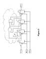
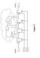
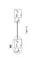
- the first illustration FIG. 1shows the circuit prior to scan insertion, and the second FIG. 2 shows the circuit after a MUXD scan insertion.
- each flip-flophas two input paths as controlled by a mux on the input.
- the scan enable “SE”When the scan enable “SE” is asserted, the scan chain operates as a shift register. This allows for each flip-flop to be set to a specific state. It also allows for the observation of each flip-flop state as the values are shifted out of the device onto the scan output “SO”.
- Each flip-flop, or scan cellis numbered for the purpose of referencing.
- the ‘and’ gatecan be tested by shifting data into scan cells 3 and 2 .
- the scan enableis de-asserted and a clock can be applied to capture the output of the combinational logic as observed at scan cell 1 .
- the scan enableis once more applied and the result data as captured at scan cell 1 is shifted through the scan chain until it arrives on the device output for the scan chain.
- testersapply a set of simulated stimulus, and validate that the response on the device outputs match the results expected from the simulation.
- Functional testersare designed to report in a go/no-go fashion that all of the outputs matched the expected results for all checked strobe points or not.
- Functional testersare not architected to understand design criteria of the device under test such as the scan structures. Thus, while functional testers can understand which output signals contained failures, each output signal can represent tens of thousands of internal scan cells.
- Another form of semiconductor testinguses optical scanning of wafers and comparison of the resultant images to identify variances from normal. These variances are reported as bounding boxes containing the geometric features that are found in some but not all wafer images. Yield management systems conduct pareto analysis to determine which defects have the greatest impact on yield and prioritize failure analysis. As processes approach and surpass 90 nanometer in feature size, optical scanning becomes less acute.
- the present inventionis a computer-implemented method to determine the physical die location of electrically failing circuit structures by combining ate fail output with layout information.
- the tangible useful result of this diagnostic processyields a list of circuit structure locations containing the faults causing a test pattern to fail. Due to the shrinking geometries and the process maturity, the diagnostic process does not stop here.
- the circuit structure locationsare further reduced to specific geometric coordinates on the die for understanding by failure analysis engineers.
- the present inventioncomprises some of the following processes: recording of automatic test equipment (ate) test failure information into a geometric database using novel and efficient compression steps which increase information, reduce storage requirements, and facilitate quicker retrieval; identifying failing scan cells in distinct name spaces used for test, logical design, and physical layout; reporting and displaying of an area on a wafer containing a fault. See FIG. 4
- FIG. 1Logic Circuit Prior to Scan Insertion
- FIG. 2Logic Circuit After Scan Insertion
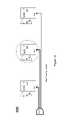
- FIG. 3Scan Chain Test
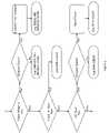
- FIG. 4Information Flowchart
- FIG. 5Flowchart for Classifying Failure Type
- FIG. 6Schematic showing an example circuit
- FIG. 7Schematic showing sample result of a FanIn Trace
- FIG. 8Schematic showing sample result of a FanOut Trace.
- FIG. 9Schematic showing result of a NetPrint Trace
- FIG. 10Schematic showing result of Tree-Trace
- FIG. 11Schematic showing result of Tree-Trace
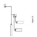
- FIG. 12Physical location of Fan-In Trace result
- Chain Integrity Testsvalidate that the scan chains are operational and can be used by the Stuck-At and AC-Scan Tests to check logic.
- Stuck-At Testsvalidate that all logic paths are operational and are not stuck to either a high or low state.
- the AC-Scan Testsvalidate that logic paths can be transitioned in suitable time to meet the mission of the device design.
- the flow chart in FIG. 5shows such an organization and categorizes the failures from these three outputs as UNRESOLVED BROKEN CHAIN, RAW STUCK, and RAW DELAY.
- the flow chartadds a decision after Chain Integrity Test failures: Analyze Chain? If this decision is true, the Blocked Chain Analysis process will be invoked to find the position in the scan chain where the block occurs. If the chain break position is found, the failures can be categorized as RESOLVED BROKEN CHAIN.
- the flow chartadds a decision after AC-Scan Test failures: Analyze Speed? If this decision is true, the SpeedScan process will be invoked to find path delay values. Once the failing paths are measured, the failures can be logged as PATH DELAY.
- the inventioncomprises a process to create a useful database consisting of the following computer implemented methods:
- a process technology for a chipmay have on or more LEF files.
- Informationsuch as MACRO size, port location, and port direction can be found in this file system.
- via descriptionscan also be found in the LEF files.
- the next step in enabling trace operations of a circuit from layout datais to convert the DEF files into a query-able format.
- the DEF filesmust be merged to together. For simplicity, each MACRO to DEF relationship defines a DEF module.
- the process of parsing the LEF and DEF filescomprises the methods following: Merging DEF Files, Concatenating Hierarchy, Recalculating XY Coordinates, Recalculating Orientation Facings, and Merging Nets.
- the process of merging DEF filesconsists of a recursive method which begins at the top DEF module. The process takes the learned list of DEF modules and compares the list against component MACRO names found in the DEF file. When a DEF module is encountered, the DEF module is then converted into a database format. This process continues recursively until there are no other DEF modules being instantiated at the leaf boundary. All DEF blocks and statements are stored in the database. Once the last leaf DEF module has been processed, the parent DEF module entries are then revised with the child DEF module expanded.
- the integration of the child module into its parent moduletakes place in the form of several processing steps. These steps include
- MACRO instance namesthat are found in the COMPONENTS section of the DEF are concatenated together.
- the resultant namecould be encoded to either shrink the size of the stored database or to provide a level of security against the interpretation of circuit intent (i.e., IP protection)
- the ultimate goal of XY coordinate recalculationis to understand an entity's placement with respect to the origin of the complete die boundary.
- the die boundaryis given in the top DEF module as the DIEAREA statement.
- the entities in a DEF file that have XY coordinatesare components, nets, specialnets, vias, and obstructions.
- the orientation conversion tableconsists of 64 possible index combinations where each index can be one of the following eight orientation facings:
- nets nameslive a double life.
- a net namecan be obfuscated like “W21” and on the other hand, the net name could be self-documenting such as “CLK2_net”.
- CLK2_netself-documenting
- the net name of the parentis used and the connection list of the child module is appended to the parent's connection list. The same is said of the XY coordinate list and via content of the route. If the port driving the net originates from within the child module, then the result of concatenating the hierarchical path to the child module and the net name of the child is used as the new net name. The new net name is stored in the parent modules database. The parent port connection list is concatenated with the child nets connection list and is associated with the new net name. Likewise, the XY net coordinate and via content in the original parent net entry are concatenated with the child net XY coordinates and via content. After the parent net information has been merged with the child net information, the original parent net entry in the parent database is deleted. The XY coordinate data of the child nets are recalculated during the merge operation.
- Each major syntax block(NETS, COMPONENTS, SPECIALNETS, MACRO, etc.) that is contained in any LEF file and/or any DEF file comprises specific block type entry statements. These statements are stored in a key-value context by using the item name as the key and the LEF or DEF description statement as the value.
- the keys that are storedcomprise:
- Values to the above keysare comprise one of a key to other database and a full content description of a DEF or LEF entry.
- At least one of the database files createdis a multi-dimensional database which enables an optimized multi-dimensional query of the LEF MACROs, PIN names, and I/O direction.
- the present embodiment of the inventionis creating query-able relationships across several database files. This manages the volume of information contained in the layout files.
- An embodiment of the storage architecturereduces and/or eliminate content duplication across the overall database structure.
- Scancell macroPI/PO, and blackbox
- ScanCell name matching and DEF component name to MACRO relationship mappingenables a third, much smaller database to be created (at compile time) which only contains scancell MACRO names. This creates a far faster lookup process than sifting through potentially hundreds of thousands of scancell names.
- the method of storing the full DEF or LEF description of major statement entries intact in particular database structuresoptimizes the assembly process of mini-DEF and mini-LEF for SPLAT representation.
- the method of storing the component names and their ports in a query-able formcomprises the steps of storing the full DEF or LEF description of major statement entries intact, manipulating the instance names of nets, ports, and components to use normalized hierarchy separators at compile time, caching macro names as a scancell, matching scancell names, and mapping DEF component names to MACRO names.
- Thisprovides the present invention a platform across multiple name spaces resolving the differences between files created for unique applications and enabling simplified access from failing scan cells identified in the test name space to the wires and components attached to them in the physical or fabrication name space.
- the Trace Engineis an optimized system for gathering circuit structures from a device design focused on electrical faults.
- the Trace Engineextracts design and layout information from STIL, LEF, and DEF files which are de jure and de facto industry standards.
- the Methods (Processes) used to gather pertinent circuit structuresare: Fan-In, Fan-Out, Net-Print, and Tree-Trace.
- the failing scancell for each blockagecan be fed into the Trace Engine using the Fan-Out Method starting at the Scan-Output from the failing scancell(s).
- the Trace Enginewill return only the circuit structures in layout format between this scancell and the next stage in the scan chain.
- the component and portcan be fed into the Trace Engine using the Net-Print Method starting at the component and port.
- the Trace Enginewill return only the circuit structures in layout format of the net associated with the component and port.
- Tree-Trace methodcan be used to localize some portion of the wide-fanin/fanout buffered tree-structures that connect to the clock, reset, or power-ground ports of the identified failing scancells.
- the Trace-Enginewill return only the circuit structures involved with the widely-distributed net that are between the failing scancell and the drive scancells, or that are common to the multiple identified failing scancells.
- Gathering of data for the purpose of yield analysismeans that data will be collected in a production environment. Any significant decrease in production throughput will reduce the benefits of potential yield improvement. Thus, a critical component of the invention is the focus on optimization.
- the size of the databasecan be limited to only the trace operations where failures have occurred while optimizing throughput to only perform each requested trace operation once.
- the Trace Engine outputidentifies a region of the die that contains many other circuit structures, such as other wire routes, vias, gates, etc.
- the Trace Engineis focused to only output the circuit structures that can be related to the fault.
- the result of the trace operationsmay be controlled by learning a trace control point list, defining filters or defining limit governors.
- the Fanin trace operationis a recursive process. Given an input port or inout port, a Fanin operation comprises the following steps:
- FIG. 7shows an example of a Fanin trace operation result. This figure shows the Fanin operation with respect to the D input of a flipflop. The trace stops at control points—scancells, blackboxes, and primary I/Os.
- FanOut trace operationalso is a recursive process. Given an output port or inout port, a FanOut operation comprises the following steps:
- FIG. 8shows an example of a FanOut trace operation result. This figure shows the FanOut with respect to the Q output of a flipflop. The trace operation stops at scancells, blackboxes, and primary I/Os.
- FIG. 9shows an example of a NetPrint trace operation result. The figure shows a net and the components connected to the net with respect to the D input of a flip-flop.
- FIGS. 10 and 11Tree Trace Process
- a methodcomprising the following steps:
- Trace ControlThe trace engine has methods to control the trace operation:
- the trace control pointis what could be called a first level control mechanism. Basically, any primary I/O, any macro that has been used as a scan cell, and any blackbox modules.
- the primary I/Ois learned from the PINS sections of the top level DEF file.
- the scan cells macrosare learned from interrogating the ScanChain descriptions from an Automatic Test Pattern Generation (ATPG) tool or other sources.
- ATPGAutomatic Test Pattern Generation
- Blackbox modulesin some cases, are inferred and in other cases require some form of user guidance either in the form of blackbox candidate specifications for LEF MACROS or by identifying either the blackbox instance name or the name of it's instantiated MACRO.
- Level 2controls set limits for the trace activity to stop. Examples of this are logic level depth, the number of ports accumulated during the trace operation, the number of nets, the number of components, and the list goes on.
- Level 3controls specifications to modify the result of the trace in some way. An example of this would be to list in sorted order the nets by the number of vias contained in the net. Or, report the trace results only if metal 7 layer is used in the net connections.
- the netlistis typically developed in a modular fashion.
- Basic circuit modulesare instantiated to create a bigger module. These modules are, in turn, used to create even bigger modules until the entire chip has defined.
- EDAelectronic design automation
- An test tool which operated on only the Verilog netlistmay describe the port to a flip flop as “ ⁇ top.core.reg1.A” and the layout tool for the same circuit may describe the same circuit location as “/top/core/reg1/A”.
- a second test toolmay describe the very same port location as “/core ⁇ .reg1.A”.
- the circuit representation that was used in the creation of the test patternmust be correlated to the component list description found in the DEF file(s). For this to occur, the hierarchical name representation must be normalized to use a common hierarchy delimiter symbol. Once the component names are in a common delimited format, then hierarchy matching methods can be applied to locate
- a computer-implemented processpicks apart the hierarchy name based on typical hierarchy delimiter symbol combinations and then re-assemble the hierarchy name with a default hierarchy delimiter symbol. Examples of a default hierarchy delimiter would be a period ‘.’ or a forward slash ‘/’.
- hierarchy names to a port or componentmay vary from one EDA tool to another.
- a hierarchy match processmust take place.
- a test toolhas referenced a scancell as “/Level0/Level1/Level2/d1”.
- the “d1”is actually a port name.
- the component name in a DEF file for that same circuitis represented like this “/Level1/Level2”.
- the present inventionis a method for determining an area on a wafer containing a fault.
- a test pattern failureobserved on automatic test equipment, creates a data log of failing output from the pattern.
- a series of transformation stepsconverts each failure to its corresponding test scan cell and thence to an instance of a physical component on a die on a wafer. Electrically, a number of wires and vias spanning multiple metal layers and components are implicated by the failing scan cell.
- the present inventioncomputes a bounding box containing these failing circuit structures suitable for analysis by yield management systems.
- FIG. 12shows bounding boxes localizing potential fault locations.
- the present inventionefficiently augments manufacturing test procedures to enable the economic analysis of electrical faults and organizes geometric information of components in a database appropriate to production test volumes and speeds. A substantial economic benefit may result from identifying causes for low yield in semiconductor manufacturing early in the product life cycle of a new process to reduce costs and improve profit.
Landscapes
- Engineering & Computer Science (AREA)
- General Engineering & Computer Science (AREA)
- Physics & Mathematics (AREA)
- General Physics & Mathematics (AREA)
- Design And Manufacture Of Integrated Circuits (AREA)
Abstract
Description
- The present application claims the benefit of priority under 35 USC .sctn. 119(e) from U.S. provisional patent application 60/829,317 filing date Oct. 13, 2006 first named inventor Dokken, titled: “A process for improving design limited quality by filtering production test data through a yield monitoring system to localize electrical faults on semiconductor wafers.”
- As manufacturing processes descend below 90 nm geometries, the well proven yield management system tools begin to lose effectiveness. In part, visibility of particulate defects is near the limit of optical inspection tools. Current yield management system tools discern correlations in areas of die which diverge from standard images. These tools cannot currently exploit understanding of the circuit functionality to geometrically locate divergences. There are also design-introduced electrical faults that are yield limiting at these tighter geometries which are detectable in the production test environment.
- To improve the testability of high density semiconductor devices, modern design practice inserts additional circuitry specific to test such as scan chains. A scan chain in test mode is configured to be a very long shift register. Patterns generated to operate with scan chains do not have any functional utility and purely observe or control potential electrical defects. But scan chain and bit have little relationship to geometrical location of the defects.
- Scan Basics
- To explain the new process, it is first necessary to provide some background on established techniques of SCAN in semiconductor test. The approach of scan methodology is to replace all flip-flops in a design with scan flip-flops. Scan flip-flops provide two paths into each flip-flop: one for the mission of the design, and a second to facilitate test.
- Scan Flip-Flops—There are two most common methods of implementation today:
- MUXD—This scan flip-flop approach places a mux on the front end of the D-input. The selector to the mux, known as the scan enable, determines whether to use the mission mode input or the scan test input.
- LSSD—Another common scan flip-flop approach is to use two clocks. One clock latches the mission path input into the flip-flop while the second clock latches the scan test input data into the flip-flop.
- Scan Chains—By stitching all of the scan flip-flops, or scan cells, together into one or more scan chains, each flip-flop can be preset or observed. This allows for test patterns to be constructed that will concentrate on finding faults in mini sub-circuits. The first illustration
FIG. 1 shows the circuit prior to scan insertion, and the secondFIG. 2 shows the circuit after a MUXD scan insertion. - In
FIG. 2 , notice that each flip-flop has two input paths as controlled by a mux on the input. When the scan enable “SE” is asserted, the scan chain operates as a shift register. This allows for each flip-flop to be set to a specific state. It also allows for the observation of each flip-flop state as the values are shifted out of the device onto the scan output “SO”. Each flip-flop, or scan cell is numbered for the purpose of referencing. - For this example, the ‘and’ gate can be tested by shifting data into
scan cells scan cell 1. The scan enable is once more applied and the result data as captured atscan cell 1 is shifted through the scan chain until it arrives on the device output for the scan chain. - Functional Tester Background
- Historically, testers apply a set of simulated stimulus, and validate that the response on the device outputs match the results expected from the simulation. Functional testers are designed to report in a go/no-go fashion that all of the outputs matched the expected results for all checked strobe points or not. Functional testers are not architected to understand design criteria of the device under test such as the scan structures. Thus, while functional testers can understand which output signals contained failures, each output signal can represent tens of thousands of internal scan cells.
- Another form of semiconductor testing uses optical scanning of wafers and comparison of the resultant images to identify variances from normal. These variances are reported as bounding boxes containing the geometric features that are found in some but not all wafer images. Yield management systems conduct pareto analysis to determine which defects have the greatest impact on yield and prioritize failure analysis. As processes approach and surpass 90 nanometer in feature size, optical scanning becomes less acute.
- Thus it can be appreciated that what is needed is a capability to translate a scan cell pattern production test failure to an area on a wafer containing a fault.
- The present invention is a computer-implemented method to determine the physical die location of electrically failing circuit structures by combining ate fail output with layout information. The tangible useful result of this diagnostic process yields a list of circuit structure locations containing the faults causing a test pattern to fail. Due to the shrinking geometries and the process maturity, the diagnostic process does not stop here. The circuit structure locations are further reduced to specific geometric coordinates on the die for understanding by failure analysis engineers.
- To report the geometric location of an electrically detected failure recorded on an automatic test equipment (ate) apparatus to a computer-implemented yield management utility software program product the invention has the following steps:
- reporting a failure type as measured by an automatic test equipment apparatus, wherein failure type, in an embodiment, comprises one of the group consisting of “unclassified”, “RAW STUCK”, “UNRESOLVED BROKEN CHAIN”, “RESOLVED BROKEN CHAIN”, “RAW DELAY”, “PATH DELAY”, and “other”;
- translating a failure location from scan chain-bit position to a logical design name for a scan cell;
- in one embodiment of the invention, tracing the components driven by the output of a scan cell;
- in a second embodiment of the invention, tracing the components driving the input of the scan cell;
- in a third embodiment of the invention, tracing the components and wires directly connected to a port on a component;
- reading a list of origins and dimensions of components and wires connecting said components; and
- computing a bounding box, wherein a bounding box comprises the maximum value and the minimum value of coordinates containing the origin and dimensions of a scan cell, at least one traced component and at least one wire connecting said traced component to the scan cell.
- The present invention comprises some of the following processes: recording of automatic test equipment (ate) test failure information into a geometric database using novel and efficient compression steps which increase information, reduce storage requirements, and facilitate quicker retrieval; identifying failing scan cells in distinct name spaces used for test, logical design, and physical layout; reporting and displaying of an area on a wafer containing a fault. See
FIG. 4 FIG. 1 . Logic Circuit Prior to Scan InsertionFIG. 2 . Logic Circuit After Scan InsertionFIG. 3 . Scan Chain TestFIG. 4 . Information FlowchartFIG. 5 . Flowchart for Classifying Failure TypeFIG. 6 . Schematic showing an example circuitFIG. 7 . Schematic showing sample result of a FanIn TraceFIG. 8 . Schematic showing sample result of a FanOut Trace.FIG. 9 . Schematic showing result of a NetPrint TraceFIG. 10 Schematic showing result of Tree-TraceFIG. 11 Schematic showing result of Tree-TraceFIG. 12 . Physical location of Fan-In Trace result- Failure Type Classification
- Semiconductor test programs are typically organized such that scan tests are divided into three areas: Chain Integrity Tests, Stuck-At Tests, and AC-Scan tests. Chain Integrity Tests validate that the scan chains are operational and can be used by the Stuck-At and AC-Scan Tests to check logic. The Stuck-At Tests validate that all logic paths are operational and are not stuck to either a high or low state. The AC-Scan Tests validate that logic paths can be transitioned in suitable time to meet the mission of the device design.
- The flow chart in
FIG. 5 shows such an organization and categorizes the failures from these three outputs as UNRESOLVED BROKEN CHAIN, RAW STUCK, and RAW DELAY. - The flow chart adds a decision after Chain Integrity Test failures: Analyze Chain? If this decision is true, the Blocked Chain Analysis process will be invoked to find the position in the scan chain where the block occurs. If the chain break position is found, the failures can be categorized as RESOLVED BROKEN CHAIN.
- The flow chart adds a decision after AC-Scan Test failures: Analyze Speed? If this decision is true, the SpeedScan process will be invoked to find path delay values. Once the failing paths are measured, the failures can be logged as PATH DELAY.
- Defect Location
- Since available data files do not identify the potential defect locations clearly, the invention comprises a process to create a useful database consisting of the following computer implemented methods:
- parsing at least one LEF file and parsing at least one DEF file, comprising the steps of
- 1. merging a plurality of DEF files;
- 2. concatenating hierarchy names;
- 3. recalculating XY coordinates;
- 4. recalculating orientation facings; and
- 5. merging nets;
and
- storing the component names of the design and their ports in a query-able form.
- parsing at least one LEF file and parsing at least one DEF file, comprising the steps of
- Multiple Name Space Resolution and Navigation
- In order to pinpoint the region on a die where a circuit structure exists, it is necessary to traverse the relationship between the implemented component list and the physical dimensions of the die. This relationship is found in the combination of DEF and LEF files. These file formats are defacto standards generally known and used by those skilled in the arts of semiconductor equipment manufacturing and electronic design automation software development. In practice this approach is too slow to be economically useful. An embodiment of the present invention uses a special built data structure.
- Parsing the LEF Files
- Tracing the layout efficiently becomes feasible by first converting the library information into a query-able format. A process technology for a chip may have on or more LEF files. Information such as MACRO size, port location, and port direction can be found in this file system. In addition, via descriptions can also be found in the LEF files.
- Parsing the DEF Files
- The next step in enabling trace operations of a circuit from layout data is to convert the DEF files into a query-able format. There may be one or more DEF files that describe the chip. If more than one DEF file is needed to describe the chip, a relationship must be identified between the MACRO name and the name of the DEF file that it is associated. The present DEF file syntax does not provide a way to communicate this relationship. Once the MACRO to DEF file relationships have been learned, the DEF files must be merged to together. For simplicity, each MACRO to DEF relationship defines a DEF module.
- The process of parsing the LEF and DEF files, comprises the methods following: Merging DEF Files, Concatenating Hierarchy, Recalculating XY Coordinates, Recalculating Orientation Facings, and Merging Nets.
- Merging DEF Files
- Several pieces of information must be managed when merging 2 or more DEF files together. The process of merging DEF files consists of a recursive method which begins at the top DEF module. The process takes the learned list of DEF modules and compares the list against component MACRO names found in the DEF file. When a DEF module is encountered, the DEF module is then converted into a database format. This process continues recursively until there are no other DEF modules being instantiated at the leaf boundary. All DEF blocks and statements are stored in the database. Once the last leaf DEF module has been processed, the parent DEF module entries are then revised with the child DEF module expanded.
- The integration of the child module into its parent module takes place in the form of several processing steps. These steps include
- concatenating component hierarchy names between parent and child module
- recalculating child component XY placement coordinate with respect to the parent modules origin
- recalculation of the child component orientation facing with respect to the target orientation facing of the parent module
- concatenating net route connection lists
- recalculation of child net route coordinates with respect to the parent module
- augmentation of the via description list with new via descriptions that were used in the net routing of the child module
- Concatenating Hierarchy
- In order to reflect the full netlist hierarchy as it was intended by the original Verilog or VHDL netlist, MACRO instance names that are found in the COMPONENTS section of the DEF are concatenated together. However, the resultant name could be encoded to either shrink the size of the stored database or to provide a level of security against the interpretation of circuit intent (i.e., IP protection)
- In addition to updating the instance name in the COMPONENTS section of the DEF, the instance names found in the connection lists of the NETS and SPECIALNETS sections must also be modified.
- Recalculating XY Coordinates
- The ultimate goal of XY coordinate recalculation is to understand an entity's placement with respect to the origin of the complete die boundary. The die boundary is given in the top DEF module as the DIEAREA statement. The entities in a DEF file that have XY coordinates are components, nets, specialnets, vias, and obstructions.
- In order to recalculate the XY coordinates associated with each of those entities, XY coordinate transform equations were developed. Inputs to these equations are
- Placement coordinate of the child module in the parent module
- Placement orientation facing of the child module in the parent module
- The DIEAREA of the child module
- XY coordinate of the child entity
Using combinations of these four inputs, XY coordinate transform equations were developed by targeting entity types. For example, a transform equation which targets COMPONENTS is not necessarily the same equation for NETS.
- Recalculating Orientation Facings
- In order to get the correct orientation facing, conversion tables use the current child component orientation and the child DEF module orientation target as lookup indexes with the conversion output being the orientation with respect to the parent module. Thus, the orientation conversion table consists of 64 possible index combinations where each index can be one of the following eight orientation facings:
- N North
- E East
- S South
- W West
- FN Flipped North
- FE Flipped East
- FS Flipped South
- FW Flipped West
- Merging Nets
- In general, nets names live a double life. On one hand, a net name can be obfuscated like “W21” and on the other hand, the net name could be self-documenting such as “CLK2_net”. When it comes to merging a child DEF module with a parent DEF module, an issue arises where two nets meet at a module boundary. To get around this issue, a merging process monitors the port directions on the net. The name of the net chosen depends on the origination of the port driving the net.
- If the port driving the net originates from the parent module, then the net name of the parent is used and the connection list of the child module is appended to the parent's connection list. The same is said of the XY coordinate list and via content of the route. If the port driving the net originates from within the child module, then the result of concatenating the hierarchical path to the child module and the net name of the child is used as the new net name. The new net name is stored in the parent modules database. The parent port connection list is concatenated with the child nets connection list and is associated with the new net name. Likewise, the XY net coordinate and via content in the original parent net entry are concatenated with the child net XY coordinates and via content. After the parent net information has been merged with the child net information, the original parent net entry in the parent database is deleted. The XY coordinate data of the child nets are recalculated during the merge operation.
- Content
- Each major syntax block (NETS, COMPONENTS, SPECIALNETS, MACRO, etc.) that is contained in any LEF file and/or any DEF file comprises specific block type entry statements. These statements are stored in a key-value context by using the item name as the key and the LEF or DEF description statement as the value.
- Various pieces of information about items at an instance name level are stored by the present invention. The keys that are stored comprise:
- Port instance name
- Net instance name
- Component instance name
- MACRO name (a.k.a., model name, module name, etc.)
- VIA name
- MACRO names that have been used as ScanCells
- Values to the above keys are comprise one of a key to other database and a full content description of a DEF or LEF entry.
- Store Process
- Various cross reference relationships are created throughout several associative arrays (key-value) database files. At least one of the database files created is a multi-dimensional database which enables an optimized multi-dimensional query of the LEF MACROs, PIN names, and I/O direction.
- Other storage architecture enhancements include content encryption and/or content compression.
- Optimizations of the Invention
- The present embodiment of the invention is creating query-able relationships across several database files. This manages the volume of information contained in the layout files. An embodiment of the storage architecture reduces and/or eliminate content duplication across the overall database structure.
- Automatic trace control (scancell macro, PI/PO, and blackbox) is controlled in-part by the method of caching macro names that have been used as a ScanCell. The combination of ScanCell name matching and DEF component name to MACRO relationship mapping enables a third, much smaller database to be created (at compile time) which only contains scancell MACRO names. This creates a far faster lookup process than sifting through potentially hundreds of thousands of scancell names.
- Since the instance names of nets, ports, and components are manipulated to use normalized hierarchy separators at compile time, this enables faster hierarchy dissection during trace operations.
- The method of storing the full DEF or LEF description of major statement entries intact in particular database structures optimizes the assembly process of mini-DEF and mini-LEF for SPLAT representation.
- The method of storing the component names and their ports in a query-able form comprises the steps of storing the full DEF or LEF description of major statement entries intact, manipulating the instance names of nets, ports, and components to use normalized hierarchy separators at compile time, caching macro names as a scancell, matching scancell names, and mapping DEF component names to MACRO names. This provides the present invention a platform across multiple name spaces resolving the differences between files created for unique applications and enabling simplified access from failing scan cells identified in the test name space to the wires and components attached to them in the physical or fabrication name space.
- The Trace Engine is an optimized system for gathering circuit structures from a device design focused on electrical faults. The Trace Engine extracts design and layout information from STIL, LEF, and DEF files which are de jure and de facto industry standards.
- The Methods (Processes) used to gather pertinent circuit structures are: Fan-In, Fan-Out, Net-Print, and Tree-Trace.
- Fan-In Objective
- When a scan test (stuck-at or ac) fails, the information reported at the tester is typically in pin and cycle-count. Once this pin and cycle-count data is converted into scan chain and bit position (scancell), the list of failing scancells can be fed into the Trace Engine using the Fan-In Method starting at the D-Input to the failing scancell(s). The Trace Engine will return only the circuit structures in layout format that lead into the failing scancell. The electrical fault likely exists within this small set of circuit structures.
- Fan-Out Objective
- When a scan chain is blocked, and if the test equipment can identify the scancell where the blockage occurs, the failing scancell for each blockage can be fed into the Trace Engine using the Fan-Out Method starting at the Scan-Output from the failing scancell(s). The Trace Engine will return only the circuit structures in layout format between this scancell and the next stage in the scan chain.
- Net-Print Objective
- When a diagnosis of failing scan data is performed and returns a fault candidate in the form of component and port, the component and port can be fed into the Trace Engine using the Net-Print Method starting at the component and port. The Trace Engine will return only the circuit structures in layout format of the net associated with the component and port.
- Tree-Trace Objective
- When an AC, scan-shift verification or delay-based scan test fails, and if the problem is identified to be related to the clock delivery, reset or the power system, then the Tree-Trace method can be used to localize some portion of the wide-fanin/fanout buffered tree-structures that connect to the clock, reset, or power-ground ports of the identified failing scancells. The Trace-Engine will return only the circuit structures involved with the widely-distributed net that are between the failing scancell and the drive scancells, or that are common to the multiple identified failing scancells.
- Gathering of data for the purpose of yield analysis means that data will be collected in a production environment. Any significant decrease in production throughput will reduce the benefits of potential yield improvement. Thus, a critical component of the invention is the focus on optimization.
- Buffer Level Limitation Optimization
- By allowing a user-definable buffer level limit for the Trace Engine, tradeoffs between circuit detail and throughput can be made
- On-Demand Execution Optimization
- Once a specific trace operation is performed for a design, that trace is remembered in a history. Thus, subsequently encountered failures that make a repeated trace request will not pay the penalty of the repeating the trace. So, the size of the database can be limited to only the trace operations where failures have occurred while optimizing throughput to only perform each requested trace operation once.
- Focus of Circuit Structure Optimization
- While the Trace Engine output identifies a region of the die that contains many other circuit structures, such as other wire routes, vias, gates, etc., the Trace Engine is focused to only output the circuit structures that can be related to the fault.
- All trace operations begin with a port name. Two ways to get the port name are.
- The port name is given explicitly as the port of a gate, register or primary input/output
- The component instance name is given and the port names are discovered from the LEF and DEF information gathered.
A port that is connected in the circuit has only one net connection. But, a net can have two or more port connections. Knowing this basic premise allows basic trace operations to occur.
- All trace operations can keep a running list of statistics about the trace result. Examples include but are not limited to:
- Port density
- Via density
- Logic Level depth
- Component density
- Via types used
- Net use types
- LEF Macros used
- Metal layers used
- Fanin Process
- The Fanin trace operation is a recursive process. Given an input port or inout port, a Fanin operation comprises the following steps:
- Discover the component name that the port belongs to and compare it to the components in the component trace cache. If a match is found, stop tracing this branch and continue tracing any unresolved branches. If no match found, add component name to the component trace cache.
- Find the net connected to the input port
- Look for output port(s) or inout port(s) connected to the net. If more than one output port exists, issue warnings because this is a potential bus contention mechanism which may cause a device to fail.
- Check to see if the component instance name associated with the output port found in
step 2 or the output port itself is part of a trace filter. If yes, perform filter dependent actions. If no, continue - Check to see if the component instance MACRO name is part of a trace control list. If yes, stop tracing this branch. If no, continue.
- Using the LEF database, discover the input ports on the component that belongs to the output port found on the net.
- For each input port found in step 5, repeat steps 1 through 4 until all trace control points have been identified and/or until filter actions have been performed.
FIG. 7 shows an example of a Fanin trace operation result. This figure shows the Fanin operation with respect to the D input of a flipflop. The trace stops at control points—scancells, blackboxes, and primary I/Os.- FanOut Process
- The FanOut trace operation also is a recursive process. Given an output port or inout port, a FanOut operation comprises the following steps:
- Discover the component name that the port belongs to and compare it to the components in the component trace cache. If a match is found, stop tracing this branch and continue tracing any unresolved branches. If no match found, add component name to the component trace cache.
- Find the net connected to the output port
- Look for input port(s) or inout port(s) connected to the net.
- For each input port found in
step 3, check to see if the component instance name associated with the input port or the input port itself is part of a trace filter. If yes, perform filter dependent actions. If no, continue - Check to see if the component instance MACRO name is part of a trace control list. If yes, stop tracing this branch. If no, continue.
- Using the LEF database, discover the output ports on the component that belongs to the input port that is being processed in step 4.
- For each output port found in step 6, repeat steps 1 through 5 until all trace control points have been identified and/or until filter actions have been performed.
FIG. 8 shows an example of a FanOut trace operation result. This figure shows the FanOut with respect to the Q output of a flipflop. The trace operation stops at scancells, blackboxes, and primary I/Os.- NetPrint Process
- This is a fundamental and essential operation. NetPrint looks up the port name and finds the name of the net attached to it. The net name is used as a lookup index in the database to retrieve the route XY coordinates, vias, and component port connection list.
FIG. 9 shows an example of a NetPrint trace operation result. The figure shows a net and the components connected to the net with respect to the D input of a flip-flop. - Tree Trace Process (
FIGS. 10 and 11 ) - A method comprising the following steps:
- Identifying a starting scancell,
- Tracing the clock input back to the output of the first buffer,
- Tracing the output of said buffer to all components touched by this output,
- Repeating for a user defined number of buffer levels, and
- Filtering the returned elements for commonality amongst failing scancells.
- Trace Control—The trace engine has methods to control the trace operation:
- setting limits for the trace activity,
- modifying the result of the trace,
- normalizing hierarchy symbols, and
- matching deviant hierarchy names.
- Trace Control Points
- The trace control point is what could be called a first level control mechanism. Basically, any primary I/O, any macro that has been used as a scan cell, and any blackbox modules. The primary I/O is learned from the PINS sections of the top level DEF file. The scan cells macros are learned from interrogating the ScanChain descriptions from an Automatic Test Pattern Generation (ATPG) tool or other sources.
- Blackbox modules, in some cases, are inferred and in other cases require some form of user guidance either in the form of blackbox candidate specifications for LEF MACROS or by identifying either the blackbox instance name or the name of it's instantiated MACRO.
- Trace Limit Governors
Level 2 controls set limits for the trace activity to stop. Examples of this are logic level depth, the number of ports accumulated during the trace operation, the number of nets, the number of components, and the list goes on.- Trace Control Filters
Level 3 controls specifications to modify the result of the trace in some way. An example of this would be to list in sorted order the nets by the number of vias contained in the net. Or, report the trace results only if metal 7 layer is used in the net connections.- Netlist Circuit Structure
- When a circuit is designed, the netlist is typically developed in a modular fashion. Basic circuit modules are instantiated to create a bigger module. These modules are, in turn, used to create even bigger modules until the entire chip has defined. To identify a port on a basic module, one would describe the absolute hierarchy path to the port. The problem with electronic design automation (EDA) tools is that they do not all use the same hierarchy delimiter symbols. An test tool which operated on only the Verilog netlist may describe the port to a flip flop as “\top.core.reg1.A” and the layout tool for the same circuit may describe the same circuit location as “/top/core/reg1/A”. Still, a second test tool may describe the very same port location as “/core\.reg1.A”.
- In order to correlate observation point failures of a test pattern to the physical space, the circuit representation that was used in the creation of the test pattern must be correlated to the component list description found in the DEF file(s). For this to occur, the hierarchical name representation must be normalized to use a common hierarchy delimiter symbol. Once the component names are in a common delimited format, then hierarchy matching methods can be applied to locate
- Normalizing Hierarchy Symbols
- To normalize the hierarchy symbols of the hierarchical reference to a component or a port name, a computer-implemented process picks apart the hierarchy name based on typical hierarchy delimiter symbol combinations and then re-assemble the hierarchy name with a default hierarchy delimiter symbol. Examples of a default hierarchy delimiter would be a period ‘.’ or a forward slash ‘/’.
- Matching Deviant Hierarchy Names
- As mentioned above, hierarchy names to a port or component may vary from one EDA tool to another. In order to compare circuit attributes from one EDA tool to the circuit attributes given by another tool, a hierarchy match process must take place. As an example, assume that a test tool has referenced a scancell as “/Level0/Level1/Level2/d1”. The “d1” is actually a port name. Now, assume that the component name in a DEF file for that same circuit is represented like this “/Level1/Level2”.
- The first observation of the example above is that a direct lookup of the scan cell name in the DEF database will yield no positive match. It is for this reason, the following computer-implemented method was developed.
- To find a name match, perform the following steps:
- 1. Converting all component names in the DEF database to use a normalized hierarchy delimiter symbol.
- 2. Converting all ScanCell name to use the same normalized hierarchy delimiter symbol that was chosen in
step 1. - 3. Dissecting the ScanCell name into it's hierarchy levels. The ScanCell name will consist of N levels. Level 0 of the is on the far left and Level N is on the far right.
- 4. Setting index j=0 and index K=N.
- 5. Computing if the ScanCell name matches any of the component names of the DEF database? If yes, a match has been found and the matching process is finished. If no, proceed to step 6.
- 6. Removing hierarchy Level K of the ScanCell name. If this action removes the hierarchy Level J, go to step 9. Else, go to step 7.
- 7. Computing if the ScanCell name match any of the component names of the DEF database? If yes, a match has been found and the matching process is finished. If no, proceed to step 8
- 8. Decrementing index K by 1. Go to step 6.
- 9. Removing Level J from the ScanCell name.
- 10. Incrementing index J by 1. Set index K=N.
- 11. If J<=N, then going to step 5. If J==N+1, then no match has been found and ending name matching process.
- The present invention is a method for determining an area on a wafer containing a fault. A test pattern failure, observed on automatic test equipment, creates a data log of failing output from the pattern. A series of transformation steps converts each failure to its corresponding test scan cell and thence to an instance of a physical component on a die on a wafer. Electrically, a number of wires and vias spanning multiple metal layers and components are implicated by the failing scan cell. The present invention computes a bounding box containing these failing circuit structures suitable for analysis by yield management systems.
FIG. 12 shows bounding boxes localizing potential fault locations. - As each scan cell may be tested tens of thousands of times, and fail a substantial number of them this process effects significant data reduction by computing one bounding box for each failing scan cell rather than each test failure.
- As manufacturing processes increase potential productivity, new processes are needed to address sources of faults which threaten to reduce yield. While visibility of particulate defects is near the limit of optical inspection tools, design-introduced electrical faults which are yield limiting at these tighter geometries begin to be significant. The present invention efficiently augments manufacturing test procedures to enable the economic analysis of electrical faults and organizes geometric information of components in a database appropriate to production test volumes and speeds. A substantial economic benefit may result from identifying causes for low yield in semiconductor manufacturing early in the product life cycle of a new process to reduce costs and improve profit.
- The scope of the invention should be determined by the appended claims and their legal equivalents, rather than the examples given to provide illustrations of presently preferred embodiments.
Claims (16)
Priority Applications (1)
| Application Number | Priority Date | Filing Date | Title |
|---|---|---|---|
| US11/682,314US8615691B2 (en) | 2006-10-13 | 2007-03-06 | Process for improving design-limited yield by localizing potential faults from production test data |
Applications Claiming Priority (2)
| Application Number | Priority Date | Filing Date | Title |
|---|---|---|---|
| US82931706P | 2006-10-13 | 2006-10-13 | |
| US11/682,314US8615691B2 (en) | 2006-10-13 | 2007-03-06 | Process for improving design-limited yield by localizing potential faults from production test data |
Publications (2)
| Publication Number | Publication Date |
|---|---|
| US20080091981A1true US20080091981A1 (en) | 2008-04-17 |
| US8615691B2 US8615691B2 (en) | 2013-12-24 |
Family
ID=39304412
Family Applications (1)
| Application Number | Title | Priority Date | Filing Date |
|---|---|---|---|
| US11/682,314Active2030-01-04US8615691B2 (en) | 2006-10-13 | 2007-03-06 | Process for improving design-limited yield by localizing potential faults from production test data |
Country Status (1)
| Country | Link |
|---|---|
| US (1) | US8615691B2 (en) |
Cited By (16)
| Publication number | Priority date | Publication date | Assignee | Title |
|---|---|---|---|---|
| US20090158225A1 (en)* | 2007-12-13 | 2009-06-18 | Jayashri Arsikere Basappa | Method and system for automatically accessing internal signals or ports in a design hierarchy |
| US20100332172A1 (en)* | 2006-03-31 | 2010-12-30 | Bruce Kaufman | Secure test-for-yield chip diagnostics management system and method |
| US20120079440A1 (en)* | 2010-09-27 | 2012-03-29 | Teseda Corporation | Suspect logical region synthesis and simulation using device design and test information |
| US8412991B2 (en) | 2011-09-02 | 2013-04-02 | Teseda Corporation | Scan chain fault diagnosis |
| US8589835B2 (en) | 2012-01-17 | 2013-11-19 | Atrenta, Inc. | System and method for inferring higher level descriptions from RTL topology based on naming similarities and dependency |
| US8656335B2 (en) | 2012-04-27 | 2014-02-18 | Atrenta, Inc. | System and methods for inferring higher level descriptions from RTL topology based on connectivity propagation |
| US8782587B2 (en) | 2012-07-30 | 2014-07-15 | Atrenta, Inc. | Systems and methods for generating a higher level description of a circuit design based on connectivity strengths |
| US8907697B2 (en) | 2011-08-31 | 2014-12-09 | Teseda Corporation | Electrical characterization for a semiconductor device pin |
| US9081932B2 (en) | 2013-02-01 | 2015-07-14 | Qualcomm Incorporated | System and method to design and test a yield sensitive circuit |
| US9355130B1 (en)* | 2012-07-26 | 2016-05-31 | Cadence Design Systems, Inc. | Method and system for component parameter management |
| US9939488B2 (en) | 2011-08-31 | 2018-04-10 | Teseda Corporation | Field triage of EOS failures in semiconductor devices |
| US10247777B1 (en) | 2016-11-10 | 2019-04-02 | Teseda Corporation | Detecting and locating shoot-through timing failures in a semiconductor integrated circuit |
| US10291413B2 (en) | 2017-02-17 | 2019-05-14 | Accenture Global Solutions Limited | Hardware blockchain corrective consensus operating procedure enforcement |
| US10298405B2 (en)* | 2017-02-17 | 2019-05-21 | Accenture Global Solutions Limited | Hardware blockchain consensus operating procedure enforcement |
| US10453549B2 (en) | 2016-12-08 | 2019-10-22 | Samsung Electronics Co., Ltd. | Memory device including virtual fail generator and memory cell repair method thereof |
| CN110968984A (en)* | 2018-09-28 | 2020-04-07 | 长鑫存储技术有限公司 | Integrated circuit process analysis system and method |
Families Citing this family (2)
| Publication number | Priority date | Publication date | Assignee | Title |
|---|---|---|---|---|
| US9922154B2 (en)* | 2016-05-20 | 2018-03-20 | International Business Machines Corporation | Enabling an incremental sign-off process using design data |
| US10622345B2 (en) | 2018-01-24 | 2020-04-14 | Honeywell International Inc. | Wafer trust via location locked circuit layout with measurable integrity |
Citations (30)
| Publication number | Priority date | Publication date | Assignee | Title |
|---|---|---|---|---|
| US3906200A (en)* | 1974-07-05 | 1975-09-16 | Sperry Rand Corp | Error logging in semiconductor storage units |
| US4839745A (en)* | 1984-06-25 | 1989-06-13 | Kirsch Technologies, Inc. | Computer memory back-up |
| US5444716A (en)* | 1993-08-30 | 1995-08-22 | At&T Corp. | Boundary-scan-based system and method for test and diagnosis |
| US5488615A (en)* | 1990-02-28 | 1996-01-30 | Ail Systems, Inc. | Universal digital signature bit device |
| US5570376A (en)* | 1994-10-05 | 1996-10-29 | Sun Microsystems, Inc. | Method and apparatus for identifying faults within a system |
| US5652754A (en)* | 1995-12-27 | 1997-07-29 | Hughes Electronics | Signature analysis usage for fault isolation |
| US5812561A (en)* | 1996-09-03 | 1998-09-22 | Motorola, Inc. | Scan based testing of an integrated circuit for compliance with timing specifications |
| US6381710B1 (en)* | 1995-04-07 | 2002-04-30 | Samsung Electronics Co., Ltd. | Error logging method utilizing temporary defect list |
| US20020073373A1 (en)* | 2000-12-13 | 2002-06-13 | Michinobu Nakao | Test method of semiconductor intergrated circuit and test pattern generator |
| US6470229B1 (en)* | 1999-12-08 | 2002-10-22 | Yield Dynamics, Inc. | Semiconductor yield management system and method |
| US20030182552A1 (en)* | 2002-03-22 | 2003-09-25 | Kouichi Tanimoto | Method of managing digital signature, apparatus for processing digital signature, and a computer readable medium for recording program of managing digital signature |
| US6629305B2 (en)* | 2000-10-03 | 2003-09-30 | Fujitsu Limited | Placement/net wiring processing system |
| US20040015803A1 (en)* | 2002-07-18 | 2004-01-22 | Huang Steve C. | Timing based scan chain implementation in an IC design |
| US20040049722A1 (en)* | 2002-09-09 | 2004-03-11 | Kabushiki Kaisha Toshiba | Failure analysis system, failure analysis method, a computer program product and a manufacturing method for a semiconductor device |
| US6748352B1 (en)* | 1999-12-30 | 2004-06-08 | Intel Corporation | Method and apparatus for scan design using a formal verification-based process |
| US20040199573A1 (en)* | 2002-10-31 | 2004-10-07 | Predictive Systems Engineering, Ltd. | System and method for remote diagnosis of distributed objects |
| US6830957B2 (en)* | 2002-09-19 | 2004-12-14 | Siliconware Precision Industries Co., Ltd. | Method of fabricating BGA packages |
| US6886140B2 (en)* | 2002-01-17 | 2005-04-26 | Micron Technology, Inc. | Fast algorithm to extract flat information from hierarchical netlists |
| US20050091621A1 (en)* | 2003-10-24 | 2005-04-28 | Goldberg David N. | Methods for designing a circuit |
| US20050229123A1 (en)* | 2001-03-30 | 2005-10-13 | Syntest Technologies, Inc. | Computer-aided design system to automate scan synthesis at register-transfer level |
| US20060066339A1 (en)* | 2004-09-06 | 2006-03-30 | Janusz Rajski | Determining and analyzing integrated circuit yield and quality |
| US20060104500A1 (en)* | 2004-11-17 | 2006-05-18 | Hitachi High-Technologies Corporation | Method and apparatus for reviewing defect of subject to be inspected |
| US7080283B1 (en)* | 2002-10-15 | 2006-07-18 | Tensilica, Inc. | Simultaneous real-time trace and debug for multiple processing core systems on a chip |
| US7146584B2 (en)* | 2001-10-30 | 2006-12-05 | Teradyne, Inc. | Scan diagnosis system and method |
| US20070038911A1 (en)* | 2005-08-01 | 2007-02-15 | Bernd Koenemann | Direct logic diagnostics with signature-based fault dictionaries |
| US7217579B2 (en)* | 2002-12-19 | 2007-05-15 | Applied Materials, Israel, Ltd. | Voltage contrast test structure |
| US20070179731A1 (en)* | 2006-01-31 | 2007-08-02 | Credence Systems Corporation | System and method for determining probing locations on ic |
| US20070220381A1 (en)* | 2006-02-17 | 2007-09-20 | Yu Huang | Enhanced diagnosis with limited failure cycles |
| US20080092003A1 (en)* | 2006-09-27 | 2008-04-17 | Ajay Khoche | Diagnostic Information Capture from Logic Devices with Built-in Self Test |
| US8453026B2 (en)* | 2006-10-13 | 2013-05-28 | Advantest (Singapore) Pte Ltd | Process for improving design limited yield by efficiently capturing and storing production test data for analysis using checksums, hash values, or digital fault signatures |
Family Cites Families (2)
| Publication number | Priority date | Publication date | Assignee | Title |
|---|---|---|---|---|
| JPH02309431A (en) | 1989-05-24 | 1990-12-25 | Nec Corp | Error output system for repeating processing |
| JP2000304820A (en)* | 1999-04-22 | 2000-11-02 | Mitsubishi Electric Corp | Failure diagnosis device, failure diagnosis method, and semiconductor integrated circuit |
- 2007
- 2007-03-06USUS11/682,314patent/US8615691B2/enactiveActive
Patent Citations (30)
| Publication number | Priority date | Publication date | Assignee | Title |
|---|---|---|---|---|
| US3906200A (en)* | 1974-07-05 | 1975-09-16 | Sperry Rand Corp | Error logging in semiconductor storage units |
| US4839745A (en)* | 1984-06-25 | 1989-06-13 | Kirsch Technologies, Inc. | Computer memory back-up |
| US5488615A (en)* | 1990-02-28 | 1996-01-30 | Ail Systems, Inc. | Universal digital signature bit device |
| US5444716A (en)* | 1993-08-30 | 1995-08-22 | At&T Corp. | Boundary-scan-based system and method for test and diagnosis |
| US5570376A (en)* | 1994-10-05 | 1996-10-29 | Sun Microsystems, Inc. | Method and apparatus for identifying faults within a system |
| US6381710B1 (en)* | 1995-04-07 | 2002-04-30 | Samsung Electronics Co., Ltd. | Error logging method utilizing temporary defect list |
| US5652754A (en)* | 1995-12-27 | 1997-07-29 | Hughes Electronics | Signature analysis usage for fault isolation |
| US5812561A (en)* | 1996-09-03 | 1998-09-22 | Motorola, Inc. | Scan based testing of an integrated circuit for compliance with timing specifications |
| US6470229B1 (en)* | 1999-12-08 | 2002-10-22 | Yield Dynamics, Inc. | Semiconductor yield management system and method |
| US6748352B1 (en)* | 1999-12-30 | 2004-06-08 | Intel Corporation | Method and apparatus for scan design using a formal verification-based process |
| US6629305B2 (en)* | 2000-10-03 | 2003-09-30 | Fujitsu Limited | Placement/net wiring processing system |
| US20020073373A1 (en)* | 2000-12-13 | 2002-06-13 | Michinobu Nakao | Test method of semiconductor intergrated circuit and test pattern generator |
| US20050229123A1 (en)* | 2001-03-30 | 2005-10-13 | Syntest Technologies, Inc. | Computer-aided design system to automate scan synthesis at register-transfer level |
| US7146584B2 (en)* | 2001-10-30 | 2006-12-05 | Teradyne, Inc. | Scan diagnosis system and method |
| US6886140B2 (en)* | 2002-01-17 | 2005-04-26 | Micron Technology, Inc. | Fast algorithm to extract flat information from hierarchical netlists |
| US20030182552A1 (en)* | 2002-03-22 | 2003-09-25 | Kouichi Tanimoto | Method of managing digital signature, apparatus for processing digital signature, and a computer readable medium for recording program of managing digital signature |
| US20040015803A1 (en)* | 2002-07-18 | 2004-01-22 | Huang Steve C. | Timing based scan chain implementation in an IC design |
| US20040049722A1 (en)* | 2002-09-09 | 2004-03-11 | Kabushiki Kaisha Toshiba | Failure analysis system, failure analysis method, a computer program product and a manufacturing method for a semiconductor device |
| US6830957B2 (en)* | 2002-09-19 | 2004-12-14 | Siliconware Precision Industries Co., Ltd. | Method of fabricating BGA packages |
| US7080283B1 (en)* | 2002-10-15 | 2006-07-18 | Tensilica, Inc. | Simultaneous real-time trace and debug for multiple processing core systems on a chip |
| US20040199573A1 (en)* | 2002-10-31 | 2004-10-07 | Predictive Systems Engineering, Ltd. | System and method for remote diagnosis of distributed objects |
| US7217579B2 (en)* | 2002-12-19 | 2007-05-15 | Applied Materials, Israel, Ltd. | Voltage contrast test structure |
| US20050091621A1 (en)* | 2003-10-24 | 2005-04-28 | Goldberg David N. | Methods for designing a circuit |
| US20060066339A1 (en)* | 2004-09-06 | 2006-03-30 | Janusz Rajski | Determining and analyzing integrated circuit yield and quality |
| US20060104500A1 (en)* | 2004-11-17 | 2006-05-18 | Hitachi High-Technologies Corporation | Method and apparatus for reviewing defect of subject to be inspected |
| US20070038911A1 (en)* | 2005-08-01 | 2007-02-15 | Bernd Koenemann | Direct logic diagnostics with signature-based fault dictionaries |
| US20070179731A1 (en)* | 2006-01-31 | 2007-08-02 | Credence Systems Corporation | System and method for determining probing locations on ic |
| US20070220381A1 (en)* | 2006-02-17 | 2007-09-20 | Yu Huang | Enhanced diagnosis with limited failure cycles |
| US20080092003A1 (en)* | 2006-09-27 | 2008-04-17 | Ajay Khoche | Diagnostic Information Capture from Logic Devices with Built-in Self Test |
| US8453026B2 (en)* | 2006-10-13 | 2013-05-28 | Advantest (Singapore) Pte Ltd | Process for improving design limited yield by efficiently capturing and storing production test data for analysis using checksums, hash values, or digital fault signatures |
Cited By (26)
| Publication number | Priority date | Publication date | Assignee | Title |
|---|---|---|---|---|
| US8626460B2 (en)* | 2006-03-31 | 2014-01-07 | Teseda Corporation | Secure test-for-yield chip diagnostics management system and method |
| US20100332172A1 (en)* | 2006-03-31 | 2010-12-30 | Bruce Kaufman | Secure test-for-yield chip diagnostics management system and method |
| US8001503B2 (en)* | 2007-12-13 | 2011-08-16 | International Business Machines Corporation | Method and system for automatically accessing internal signals or ports in a design hierarchy |
| US20090158225A1 (en)* | 2007-12-13 | 2009-06-18 | Jayashri Arsikere Basappa | Method and system for automatically accessing internal signals or ports in a design hierarchy |
| US20120079440A1 (en)* | 2010-09-27 | 2012-03-29 | Teseda Corporation | Suspect logical region synthesis and simulation using device design and test information |
| US20120079442A1 (en)* | 2010-09-27 | 2012-03-29 | Teseda Corporation | Correlation of device manufacturing defect data with device electrical test data |
| US9659136B2 (en) | 2010-09-27 | 2017-05-23 | Teseda Corporation | Suspect logical region synthesis from device design and test information |
| US8453088B2 (en)* | 2010-09-27 | 2013-05-28 | Teseda Corporation | Suspect logical region synthesis and simulation using device design and test information |
| US8539389B2 (en)* | 2010-09-27 | 2013-09-17 | Teseda Corporation | Correlation of device manufacturing defect data with device electrical test data |
| US8918753B2 (en) | 2010-09-27 | 2014-12-23 | Teseda Corporation | Correlation of device manufacturing defect data with device electrical test data |
| US9939488B2 (en) | 2011-08-31 | 2018-04-10 | Teseda Corporation | Field triage of EOS failures in semiconductor devices |
| US8907697B2 (en) | 2011-08-31 | 2014-12-09 | Teseda Corporation | Electrical characterization for a semiconductor device pin |
| US8892972B2 (en) | 2011-09-02 | 2014-11-18 | Teseda Corporation | Scan chain fault diagnosis |
| US8560904B2 (en) | 2011-09-02 | 2013-10-15 | Teseda Corporation | Scan chain fault diagnosis |
| US8412991B2 (en) | 2011-09-02 | 2013-04-02 | Teseda Corporation | Scan chain fault diagnosis |
| US8589835B2 (en) | 2012-01-17 | 2013-11-19 | Atrenta, Inc. | System and method for inferring higher level descriptions from RTL topology based on naming similarities and dependency |
| US8813003B2 (en) | 2012-01-17 | 2014-08-19 | Atrenta, Inc. | System and method for inferring higher level descriptions from RTL topology based on naming similarities and dependency |
| US8656335B2 (en) | 2012-04-27 | 2014-02-18 | Atrenta, Inc. | System and methods for inferring higher level descriptions from RTL topology based on connectivity propagation |
| US9355130B1 (en)* | 2012-07-26 | 2016-05-31 | Cadence Design Systems, Inc. | Method and system for component parameter management |
| US8782587B2 (en) | 2012-07-30 | 2014-07-15 | Atrenta, Inc. | Systems and methods for generating a higher level description of a circuit design based on connectivity strengths |
| US9081932B2 (en) | 2013-02-01 | 2015-07-14 | Qualcomm Incorporated | System and method to design and test a yield sensitive circuit |
| US10247777B1 (en) | 2016-11-10 | 2019-04-02 | Teseda Corporation | Detecting and locating shoot-through timing failures in a semiconductor integrated circuit |
| US10453549B2 (en) | 2016-12-08 | 2019-10-22 | Samsung Electronics Co., Ltd. | Memory device including virtual fail generator and memory cell repair method thereof |
| US10291413B2 (en) | 2017-02-17 | 2019-05-14 | Accenture Global Solutions Limited | Hardware blockchain corrective consensus operating procedure enforcement |
| US10298405B2 (en)* | 2017-02-17 | 2019-05-21 | Accenture Global Solutions Limited | Hardware blockchain consensus operating procedure enforcement |
| CN110968984A (en)* | 2018-09-28 | 2020-04-07 | 长鑫存储技术有限公司 | Integrated circuit process analysis system and method |
Also Published As
| Publication number | Publication date |
|---|---|
| US8615691B2 (en) | 2013-12-24 |
Similar Documents
| Publication | Publication Date | Title |
|---|---|---|
| US8615691B2 (en) | Process for improving design-limited yield by localizing potential faults from production test data | |
| JP5311818B2 (en) | Compactor-independent fault diagnosis | |
| JP4791954B2 (en) | Test response compression using compactors | |
| US7870519B2 (en) | Method for determining features associated with fails of integrated circuits | |
| US20040205681A1 (en) | Calculation system of fault coverage and calculation method of the same | |
| US7610568B2 (en) | Methods and apparatus for making placement sensitive logic modifications | |
| US8504968B2 (en) | Method to determine high level power distribution and interface problems in complex integrated circuits | |
| US10657207B1 (en) | Inter-cell bridge defect diagnosis | |
| CN1342318A (en) | IC test software system for mapping logical functional data of logic integrated circuits to physical representation | |
| US5796990A (en) | Hierarchical fault modeling system and method | |
| Gupta et al. | Integrating a boolean satisfiability checker and bdds for combinational equivalence checking | |
| US20030221173A1 (en) | Method and apparatus for detecting connectivity conditions in a netlist database | |
| US6449751B1 (en) | Method of analyzing static current test vectors with reduced file sizes for semiconductor integrated circuits | |
| Kokrady et al. | Fast, layout-aware validation of test-vectors for nanometer-related timing failures | |
| US10234502B1 (en) | Circuit defect diagnosis based on sink cell fault models | |
| Huang et al. | Non-adaptive pattern reordering to improve scan chain diagnostic resolution | |
| US11740284B1 (en) | Diagnosing multicycle faults and/or defects with single cycle ATPG test patterns | |
| Zou et al. | Speeding up effect-cause defect diagnosis using a small dictionary | |
| Agrawal et al. | Redundancy identification using transitive closure | |
| Urban et al. | Global Control Signal Defect Diagnosis in Volume Production Environment | |
| US20070204192A1 (en) | Method for detecting defects of a chip | |
| Chandrasekar et al. | Search State Compatibility based Incremental Learning Framework and output deviation based X-filling for diagnostic test generation | |
| Salinas et al. | A sweeping line approach to interconnect testing | |
| Narayanan et al. | A Fault Diagnosis Methodology for the UltraSPARC/sup TM/-I microprocessor | |
| US12007440B1 (en) | Systems and methods for scan chain stitching |
Legal Events
| Date | Code | Title | Description |
|---|---|---|---|
| AS | Assignment | Owner name:INOVYS CORPORATION, CALIFORNIA Free format text:ASSIGNMENT OF ASSIGNORS INTEREST;ASSIGNORS:DOKKEN, RICHARD C.;CHAN, GERALD S.;POTTER, JOHN C.;AND OTHERS;REEL/FRAME:021636/0185;SIGNING DATES FROM 20080820 TO 20080828 Owner name:INOVYS CORPORATION, CALIFORNIA Free format text:ASSIGNMENT OF ASSIGNORS INTEREST;ASSIGNORS:DOKKEN, RICHARD C.;CHAN, GERALD S.;POTTER, JOHN C.;AND OTHERS;SIGNING DATES FROM 20080820 TO 20080828;REEL/FRAME:021636/0185 | |
| AS | Assignment | Owner name:VERIGY (SINGAPORE) PTE. LTD., SINGAPORE Free format text:ASSIGNMENT OF ASSIGNORS INTEREST;ASSIGNOR:INOVYS CORPORATION;REEL/FRAME:023330/0760 Effective date:20091006 Owner name:VERIGY (SINGAPORE) PTE. LTD.,SINGAPORE Free format text:ASSIGNMENT OF ASSIGNORS INTEREST;ASSIGNOR:INOVYS CORPORATION;REEL/FRAME:023330/0760 Effective date:20091006 | |
| AS | Assignment | Owner name:ADVANTEST (SINGAPORE) PTE LTD, SINGAPORE Free format text:ASSIGNMENT OF ASSIGNORS INTEREST;ASSIGNOR:VERIGY (SINGAPORE) PTE LTD;REEL/FRAME:027896/0018 Effective date:20120302 | |
| STCF | Information on status: patent grant | Free format text:PATENTED CASE | |
| AS | Assignment | Owner name:ADVANTEST CORPORATION, JAPAN Free format text:ASSIGNMENT OF ASSIGNORS INTEREST;ASSIGNOR:ADVANTEST (SINGAPORE) PTE. LTD.;REEL/FRAME:035371/0265 Effective date:20150401 | |
| AS | Assignment | Owner name:ADVANTEST CORPORATION, JAPAN Free format text:CORRECTIVE ASSIGNMENT TO CORRECT THE ASSIGNEE ADDRESS PREVIOUSLY RECORDED AT REEL: 035371 FRAME: 0265. ASSIGNOR(S) HEREBY CONFIRMS THE ASSIGNMENT;ASSIGNOR:ADVANTEST (SINGAPORE) PTE. LTD.;REEL/FRAME:035425/0768 Effective date:20150401 | |
| FPAY | Fee payment | Year of fee payment:4 | |
| AS | Assignment | Owner name:ADVANTEST CORPORATION, JAPAN Free format text:CHANGE OF ADDRESS;ASSIGNOR:ADVANTEST CORPORATION;REEL/FRAME:047987/0626 Effective date:20181112 | |
| MAFP | Maintenance fee payment | Free format text:PAYMENT OF MAINTENANCE FEE, 8TH YEAR, LARGE ENTITY (ORIGINAL EVENT CODE: M1552); ENTITY STATUS OF PATENT OWNER: LARGE ENTITY Year of fee payment:8 | |
| MAFP | Maintenance fee payment | Free format text:PAYMENT OF MAINTENANCE FEE, 12TH YEAR, LARGE ENTITY (ORIGINAL EVENT CODE: M1553); ENTITY STATUS OF PATENT OWNER: LARGE ENTITY Year of fee payment:12 |