US20080088003A1 - Stacked Modules and Method - Google Patents
Stacked Modules and MethodDownload PDFInfo
- Publication number
- US20080088003A1 US20080088003A1US11/873,351US87335107AUS2008088003A1US 20080088003 A1US20080088003 A1US 20080088003A1US 87335107 AUS87335107 AUS 87335107AUS 2008088003 A1US2008088003 A1US 2008088003A1
- Authority
- US
- United States
- Prior art keywords
- csp
- flex
- contacts
- assembly
- circuit
- Prior art date
- Legal status (The legal status is an assumption and is not a legal conclusion. Google has not performed a legal analysis and makes no representation as to the accuracy of the status listed.)
- Granted
Links
Images


Classifications
- H—ELECTRICITY
- H01—ELECTRIC ELEMENTS
- H01L—SEMICONDUCTOR DEVICES NOT COVERED BY CLASS H10
- H01L25/00—Assemblies consisting of a plurality of semiconductor or other solid state devices
- H01L25/03—Assemblies consisting of a plurality of semiconductor or other solid state devices all the devices being of a type provided for in a single subclass of subclasses H10B, H10D, H10F, H10H, H10K or H10N, e.g. assemblies of rectifier diodes
- H01L25/10—Assemblies consisting of a plurality of semiconductor or other solid state devices all the devices being of a type provided for in a single subclass of subclasses H10B, H10D, H10F, H10H, H10K or H10N, e.g. assemblies of rectifier diodes the devices having separate containers
- H01L25/105—Assemblies consisting of a plurality of semiconductor or other solid state devices all the devices being of a type provided for in a single subclass of subclasses H10B, H10D, H10F, H10H, H10K or H10N, e.g. assemblies of rectifier diodes the devices having separate containers the devices being integrated devices of class H10
- H—ELECTRICITY
- H01—ELECTRIC ELEMENTS
- H01L—SEMICONDUCTOR DEVICES NOT COVERED BY CLASS H10
- H01L21/00—Processes or apparatus adapted for the manufacture or treatment of semiconductor or solid state devices or of parts thereof
- H01L21/02—Manufacture or treatment of semiconductor devices or of parts thereof
- H01L21/04—Manufacture or treatment of semiconductor devices or of parts thereof the devices having potential barriers, e.g. a PN junction, depletion layer or carrier concentration layer
- H01L21/48—Manufacture or treatment of parts, e.g. containers, prior to assembly of the devices, using processes not provided for in a single one of the groups H01L21/18 - H01L21/326 or H10D48/04 - H10D48/07
- H01L21/4814—Conductive parts
- H01L21/4871—Bases, plates or heatsinks
- H—ELECTRICITY
- H01—ELECTRIC ELEMENTS
- H01L—SEMICONDUCTOR DEVICES NOT COVERED BY CLASS H10
- H01L23/00—Details of semiconductor or other solid state devices
- H01L23/28—Encapsulations, e.g. encapsulating layers, coatings, e.g. for protection
- H01L23/31—Encapsulations, e.g. encapsulating layers, coatings, e.g. for protection characterised by the arrangement or shape
- H01L23/3107—Encapsulations, e.g. encapsulating layers, coatings, e.g. for protection characterised by the arrangement or shape the device being completely enclosed
- H01L23/3114—Encapsulations, e.g. encapsulating layers, coatings, e.g. for protection characterised by the arrangement or shape the device being completely enclosed the device being a chip scale package, e.g. CSP
- H—ELECTRICITY
- H01—ELECTRIC ELEMENTS
- H01L—SEMICONDUCTOR DEVICES NOT COVERED BY CLASS H10
- H01L23/00—Details of semiconductor or other solid state devices
- H01L23/48—Arrangements for conducting electric current to or from the solid state body in operation, e.g. leads, terminal arrangements ; Selection of materials therefor
- H01L23/488—Arrangements for conducting electric current to or from the solid state body in operation, e.g. leads, terminal arrangements ; Selection of materials therefor consisting of soldered or bonded constructions
- H01L23/498—Leads, i.e. metallisations or lead-frames on insulating substrates, e.g. chip carriers
- H01L23/49833—Leads, i.e. metallisations or lead-frames on insulating substrates, e.g. chip carriers the chip support structure consisting of a plurality of insulating substrates
- H—ELECTRICITY
- H01—ELECTRIC ELEMENTS
- H01L—SEMICONDUCTOR DEVICES NOT COVERED BY CLASS H10
- H01L23/00—Details of semiconductor or other solid state devices
- H01L23/48—Arrangements for conducting electric current to or from the solid state body in operation, e.g. leads, terminal arrangements ; Selection of materials therefor
- H01L23/488—Arrangements for conducting electric current to or from the solid state body in operation, e.g. leads, terminal arrangements ; Selection of materials therefor consisting of soldered or bonded constructions
- H01L23/498—Leads, i.e. metallisations or lead-frames on insulating substrates, e.g. chip carriers
- H01L23/4985—Flexible insulating substrates
- H—ELECTRICITY
- H01—ELECTRIC ELEMENTS
- H01L—SEMICONDUCTOR DEVICES NOT COVERED BY CLASS H10
- H01L23/00—Details of semiconductor or other solid state devices
- H01L23/52—Arrangements for conducting electric current within the device in operation from one component to another, i.e. interconnections, e.g. wires, lead frames
- H01L23/538—Arrangements for conducting electric current within the device in operation from one component to another, i.e. interconnections, e.g. wires, lead frames the interconnection structure between a plurality of semiconductor chips being formed on, or in, insulating substrates
- H01L23/5385—Assembly of a plurality of insulating substrates
- H—ELECTRICITY
- H01—ELECTRIC ELEMENTS
- H01L—SEMICONDUCTOR DEVICES NOT COVERED BY CLASS H10
- H01L2224/00—Indexing scheme for arrangements for connecting or disconnecting semiconductor or solid-state bodies and methods related thereto as covered by H01L24/00
- H01L2224/01—Means for bonding being attached to, or being formed on, the surface to be connected, e.g. chip-to-package, die-attach, "first-level" interconnects; Manufacturing methods related thereto
- H01L2224/10—Bump connectors; Manufacturing methods related thereto
- H01L2224/15—Structure, shape, material or disposition of the bump connectors after the connecting process
- H01L2224/16—Structure, shape, material or disposition of the bump connectors after the connecting process of an individual bump connector
- H01L2224/161—Disposition
- H01L2224/16151—Disposition the bump connector connecting between a semiconductor or solid-state body and an item not being a semiconductor or solid-state body, e.g. chip-to-substrate, chip-to-passive
- H01L2224/16221—Disposition the bump connector connecting between a semiconductor or solid-state body and an item not being a semiconductor or solid-state body, e.g. chip-to-substrate, chip-to-passive the body and the item being stacked
- H01L2224/16225—Disposition the bump connector connecting between a semiconductor or solid-state body and an item not being a semiconductor or solid-state body, e.g. chip-to-substrate, chip-to-passive the body and the item being stacked the item being non-metallic, e.g. insulating substrate with or without metallisation
- H—ELECTRICITY
- H01—ELECTRIC ELEMENTS
- H01L—SEMICONDUCTOR DEVICES NOT COVERED BY CLASS H10
- H01L2224/00—Indexing scheme for arrangements for connecting or disconnecting semiconductor or solid-state bodies and methods related thereto as covered by H01L24/00
- H01L2224/01—Means for bonding being attached to, or being formed on, the surface to be connected, e.g. chip-to-package, die-attach, "first-level" interconnects; Manufacturing methods related thereto
- H01L2224/26—Layer connectors, e.g. plate connectors, solder or adhesive layers; Manufacturing methods related thereto
- H01L2224/31—Structure, shape, material or disposition of the layer connectors after the connecting process
- H01L2224/32—Structure, shape, material or disposition of the layer connectors after the connecting process of an individual layer connector
- H01L2224/321—Disposition
- H01L2224/32151—Disposition the layer connector connecting between a semiconductor or solid-state body and an item not being a semiconductor or solid-state body, e.g. chip-to-substrate, chip-to-passive
- H01L2224/32221—Disposition the layer connector connecting between a semiconductor or solid-state body and an item not being a semiconductor or solid-state body, e.g. chip-to-substrate, chip-to-passive the body and the item being stacked
- H01L2224/32225—Disposition the layer connector connecting between a semiconductor or solid-state body and an item not being a semiconductor or solid-state body, e.g. chip-to-substrate, chip-to-passive the body and the item being stacked the item being non-metallic, e.g. insulating substrate with or without metallisation
- H—ELECTRICITY
- H01—ELECTRIC ELEMENTS
- H01L—SEMICONDUCTOR DEVICES NOT COVERED BY CLASS H10
- H01L2224/00—Indexing scheme for arrangements for connecting or disconnecting semiconductor or solid-state bodies and methods related thereto as covered by H01L24/00
- H01L2224/73—Means for bonding being of different types provided for in two or more of groups H01L2224/10, H01L2224/18, H01L2224/26, H01L2224/34, H01L2224/42, H01L2224/50, H01L2224/63, H01L2224/71
- H01L2224/732—Location after the connecting process
- H01L2224/73201—Location after the connecting process on the same surface
- H01L2224/73203—Bump and layer connectors
- H01L2224/73204—Bump and layer connectors the bump connector being embedded into the layer connector
- H—ELECTRICITY
- H01—ELECTRIC ELEMENTS
- H01L—SEMICONDUCTOR DEVICES NOT COVERED BY CLASS H10
- H01L2224/00—Indexing scheme for arrangements for connecting or disconnecting semiconductor or solid-state bodies and methods related thereto as covered by H01L24/00
- H01L2224/73—Means for bonding being of different types provided for in two or more of groups H01L2224/10, H01L2224/18, H01L2224/26, H01L2224/34, H01L2224/42, H01L2224/50, H01L2224/63, H01L2224/71
- H01L2224/732—Location after the connecting process
- H01L2224/73251—Location after the connecting process on different surfaces
- H01L2224/73253—Bump and layer connectors
- H—ELECTRICITY
- H01—ELECTRIC ELEMENTS
- H01L—SEMICONDUCTOR DEVICES NOT COVERED BY CLASS H10
- H01L2225/00—Details relating to assemblies covered by the group H01L25/00 but not provided for in its subgroups
- H01L2225/03—All the devices being of a type provided for in the same main group of the same subclass of class H10, e.g. assemblies of rectifier diodes
- H01L2225/04—All the devices being of a type provided for in the same main group of the same subclass of class H10, e.g. assemblies of rectifier diodes the devices not having separate containers
- H01L2225/065—All the devices being of a type provided for in the same main group of the same subclass of class H10
- H01L2225/06503—Stacked arrangements of devices
- H01L2225/06517—Bump or bump-like direct electrical connections from device to substrate
- H—ELECTRICITY
- H01—ELECTRIC ELEMENTS
- H01L—SEMICONDUCTOR DEVICES NOT COVERED BY CLASS H10
- H01L2225/00—Details relating to assemblies covered by the group H01L25/00 but not provided for in its subgroups
- H01L2225/03—All the devices being of a type provided for in the same main group of the same subclass of class H10, e.g. assemblies of rectifier diodes
- H01L2225/04—All the devices being of a type provided for in the same main group of the same subclass of class H10, e.g. assemblies of rectifier diodes the devices not having separate containers
- H01L2225/065—All the devices being of a type provided for in the same main group of the same subclass of class H10
- H01L2225/06503—Stacked arrangements of devices
- H01L2225/06541—Conductive via connections through the device, e.g. vertical interconnects, through silicon via [TSV]
- H—ELECTRICITY
- H01—ELECTRIC ELEMENTS
- H01L—SEMICONDUCTOR DEVICES NOT COVERED BY CLASS H10
- H01L2225/00—Details relating to assemblies covered by the group H01L25/00 but not provided for in its subgroups
- H01L2225/03—All the devices being of a type provided for in the same main group of the same subclass of class H10, e.g. assemblies of rectifier diodes
- H01L2225/04—All the devices being of a type provided for in the same main group of the same subclass of class H10, e.g. assemblies of rectifier diodes the devices not having separate containers
- H01L2225/065—All the devices being of a type provided for in the same main group of the same subclass of class H10
- H01L2225/06503—Stacked arrangements of devices
- H01L2225/06579—TAB carriers; beam leads
- H—ELECTRICITY
- H01—ELECTRIC ELEMENTS
- H01L—SEMICONDUCTOR DEVICES NOT COVERED BY CLASS H10
- H01L2225/00—Details relating to assemblies covered by the group H01L25/00 but not provided for in its subgroups
- H01L2225/03—All the devices being of a type provided for in the same main group of the same subclass of class H10, e.g. assemblies of rectifier diodes
- H01L2225/04—All the devices being of a type provided for in the same main group of the same subclass of class H10, e.g. assemblies of rectifier diodes the devices not having separate containers
- H01L2225/065—All the devices being of a type provided for in the same main group of the same subclass of class H10
- H01L2225/06503—Stacked arrangements of devices
- H01L2225/06582—Housing for the assembly, e.g. chip scale package [CSP]
- H01L2225/06586—Housing with external bump or bump-like connectors
- H—ELECTRICITY
- H01—ELECTRIC ELEMENTS
- H01L—SEMICONDUCTOR DEVICES NOT COVERED BY CLASS H10
- H01L2225/00—Details relating to assemblies covered by the group H01L25/00 but not provided for in its subgroups
- H01L2225/03—All the devices being of a type provided for in the same main group of the same subclass of class H10, e.g. assemblies of rectifier diodes
- H01L2225/10—All the devices being of a type provided for in the same main group of the same subclass of class H10, e.g. assemblies of rectifier diodes the devices having separate containers
- H01L2225/1005—All the devices being of a type provided for in the same main group of the same subclass of class H10, e.g. assemblies of rectifier diodes the devices having separate containers the devices being integrated devices of class H10
- H01L2225/1011—All the devices being of a type provided for in the same main group of the same subclass of class H10, e.g. assemblies of rectifier diodes the devices having separate containers the devices being integrated devices of class H10 the containers being in a stacked arrangement
- H01L2225/1047—Details of electrical connections between containers
- H01L2225/107—Indirect electrical connections, e.g. via an interposer, a flexible substrate, using TAB
- H—ELECTRICITY
- H01—ELECTRIC ELEMENTS
- H01L—SEMICONDUCTOR DEVICES NOT COVERED BY CLASS H10
- H01L23/00—Details of semiconductor or other solid state devices
- H01L23/48—Arrangements for conducting electric current to or from the solid state body in operation, e.g. leads, terminal arrangements ; Selection of materials therefor
- H01L23/488—Arrangements for conducting electric current to or from the solid state body in operation, e.g. leads, terminal arrangements ; Selection of materials therefor consisting of soldered or bonded constructions
- H01L23/498—Leads, i.e. metallisations or lead-frames on insulating substrates, e.g. chip carriers
- H01L23/49838—Geometry or layout
- H—ELECTRICITY
- H01—ELECTRIC ELEMENTS
- H01L—SEMICONDUCTOR DEVICES NOT COVERED BY CLASS H10
- H01L23/00—Details of semiconductor or other solid state devices
- H01L23/52—Arrangements for conducting electric current within the device in operation from one component to another, i.e. interconnections, e.g. wires, lead frames
- H01L23/538—Arrangements for conducting electric current within the device in operation from one component to another, i.e. interconnections, e.g. wires, lead frames the interconnection structure between a plurality of semiconductor chips being formed on, or in, insulating substrates
- H01L23/5387—Flexible insulating substrates
- H—ELECTRICITY
- H01—ELECTRIC ELEMENTS
- H01L—SEMICONDUCTOR DEVICES NOT COVERED BY CLASS H10
- H01L24/00—Arrangements for connecting or disconnecting semiconductor or solid-state bodies; Methods or apparatus related thereto
- H01L24/01—Means for bonding being attached to, or being formed on, the surface to be connected, e.g. chip-to-package, die-attach, "first-level" interconnects; Manufacturing methods related thereto
- H01L24/10—Bump connectors ; Manufacturing methods related thereto
- H01L24/15—Structure, shape, material or disposition of the bump connectors after the connecting process
- H01L24/16—Structure, shape, material or disposition of the bump connectors after the connecting process of an individual bump connector
- H—ELECTRICITY
- H01—ELECTRIC ELEMENTS
- H01L—SEMICONDUCTOR DEVICES NOT COVERED BY CLASS H10
- H01L2924/00—Indexing scheme for arrangements or methods for connecting or disconnecting semiconductor or solid-state bodies as covered by H01L24/00
- H01L2924/0001—Technical content checked by a classifier
- H01L2924/00011—Not relevant to the scope of the group, the symbol of which is combined with the symbol of this group
- H—ELECTRICITY
- H01—ELECTRIC ELEMENTS
- H01L—SEMICONDUCTOR DEVICES NOT COVERED BY CLASS H10
- H01L2924/00—Indexing scheme for arrangements or methods for connecting or disconnecting semiconductor or solid-state bodies as covered by H01L24/00
- H01L2924/0001—Technical content checked by a classifier
- H01L2924/00014—Technical content checked by a classifier the subject-matter covered by the group, the symbol of which is combined with the symbol of this group, being disclosed without further technical details
- H—ELECTRICITY
- H01—ELECTRIC ELEMENTS
- H01L—SEMICONDUCTOR DEVICES NOT COVERED BY CLASS H10
- H01L2924/00—Indexing scheme for arrangements or methods for connecting or disconnecting semiconductor or solid-state bodies as covered by H01L24/00
- H01L2924/10—Details of semiconductor or other solid state devices to be connected
- H01L2924/11—Device type
- H01L2924/14—Integrated circuits
- H—ELECTRICITY
- H01—ELECTRIC ELEMENTS
- H01L—SEMICONDUCTOR DEVICES NOT COVERED BY CLASS H10
- H01L2924/00—Indexing scheme for arrangements or methods for connecting or disconnecting semiconductor or solid-state bodies as covered by H01L24/00
- H01L2924/30—Technical effects
- H01L2924/35—Mechanical effects
- H01L2924/351—Thermal stress
- H01L2924/3511—Warping
- Y—GENERAL TAGGING OF NEW TECHNOLOGICAL DEVELOPMENTS; GENERAL TAGGING OF CROSS-SECTIONAL TECHNOLOGIES SPANNING OVER SEVERAL SECTIONS OF THE IPC; TECHNICAL SUBJECTS COVERED BY FORMER USPC CROSS-REFERENCE ART COLLECTIONS [XRACs] AND DIGESTS
- Y10—TECHNICAL SUBJECTS COVERED BY FORMER USPC
- Y10T—TECHNICAL SUBJECTS COVERED BY FORMER US CLASSIFICATION
- Y10T29/00—Metal working
- Y10T29/49—Method of mechanical manufacture
- Y10T29/49002—Electrical device making
- Y10T29/49117—Conductor or circuit manufacturing
- Y10T29/49169—Assembling electrical component directly to terminal or elongated conductor
- Y—GENERAL TAGGING OF NEW TECHNOLOGICAL DEVELOPMENTS; GENERAL TAGGING OF CROSS-SECTIONAL TECHNOLOGIES SPANNING OVER SEVERAL SECTIONS OF THE IPC; TECHNICAL SUBJECTS COVERED BY FORMER USPC CROSS-REFERENCE ART COLLECTIONS [XRACs] AND DIGESTS
- Y10—TECHNICAL SUBJECTS COVERED BY FORMER USPC
- Y10T—TECHNICAL SUBJECTS COVERED BY FORMER US CLASSIFICATION
- Y10T29/00—Metal working
- Y10T29/53—Means to assemble or disassemble
- Y10T29/5313—Means to assemble electrical device
- Y10T29/532—Conductor
- Y10T29/53209—Terminal or connector
- Y—GENERAL TAGGING OF NEW TECHNOLOGICAL DEVELOPMENTS; GENERAL TAGGING OF CROSS-SECTIONAL TECHNOLOGIES SPANNING OVER SEVERAL SECTIONS OF THE IPC; TECHNICAL SUBJECTS COVERED BY FORMER USPC CROSS-REFERENCE ART COLLECTIONS [XRACs] AND DIGESTS
- Y10—TECHNICAL SUBJECTS COVERED BY FORMER USPC
- Y10T—TECHNICAL SUBJECTS COVERED BY FORMER US CLASSIFICATION
- Y10T29/00—Metal working
- Y10T29/53—Means to assemble or disassemble
- Y10T29/5313—Means to assemble electrical device
- Y10T29/5327—Means to fasten by deforming
Definitions
- the present inventionrelates to aggregating integrated circuits and, in particular, to stacking integrated circuits in chip-scale packages and methods for creating stacked modules of chip-scale packages.
- a variety of techniquesare used to stack packaged integrated circuits. Some methods require special packages, while other techniques stack packages configured to allow stand-alone deployment in an operating environment.
- Chip scale packagingrefers generally to packages that provide connection to an integrated circuit through a set of contacts (often embodied as “bumps” or “balls”) arrayed across a major surface of the package. Instead of leads emergent from a peripheral side of the package as in “leaded” packages, in a CSP, contacts are placed on a major surface and typically emerge from the planar bottom surface of the package. The absence of “leads” on package sides renders most stacking techniques devised for leaded packages inapplicable for CSP stacking.
- CSPhas enabled reductions in size and weight parameters for many applications.
- CSPis a broad category including a variety of packages from near chip scale to die-sized packages such as the die sized ball grid array (DSBGA).
- DSBGAdie sized ball grid array
- Staktek Group L.P.the assignee of the present invention, has developed a variety of stacked module designs that employ a form standard or mandrel that can provide thermal and/or construction advantages while providing a standard form that may allow use of a flexible circuit design with a variety of CSP types and body sizes.
- the mandrel or form standard stack designscome in a variety of shapes and sizes and materials.
- Some form standardsextend beyond the perimeter edge or the extent of the CSP body and thus provide a form about which the flex circuitry transits.
- Some other form standardsare substantially planar and have a lateral extent smaller than the lateral extent of an adjacent CSP.
- Stacked module design and assembly techniques and systemsthat provide a thermally efficient, reliable structure that perform well at higher frequencies but do not add excessive height to the stack that can be manufactured at reasonable cost with readily understood and managed materials and methods are provided.
- the present inventionallows chip scale-packaged integrated circuits (CSPs) that are configured to allow stand-alone deployment in an operating environment to instead be stacked into modules that conserve PWB or other board surface area.
- CSPschip scale-packaged integrated circuits
- the present inventioncan be used to advantage with CSP packages of a variety of sizes and configurations ranging from typical BGAs with footprints somewhat larger than the contained die to smaller packages such as, for example, die-sized packages such as DSBGA.
- the present inventionis applied most frequently to chip scale packages that contain one die, it may be employed with chip scale packages that include more than one integrated circuit die.
- two CSPsare stacked, with one CSP disposed above the other.
- the two CSPsare connected with a pair of flex circuits.
- Each of the pair of flex circuitsis partially wrapped about a respective opposite lateral edge of the lower CSP of the module.
- the flex circuit pairconnects the upper and lower CSPs and provides a thermal and electrical path connection path between the module and an application environment such as a printed wiring board (PWB).
- PWBprinted wiring board
- a precursor assembly for use as a component of a stacked circuit modulehaving a CSP and a flex circuit with one or more stiffeners attached to the flex circuit.
- the stiffenersare disposed along a major surface of the CSP and may be attached to the major surface of the CSP by adhesive.
- Exemplary stacked circuit modules devised in accordance with a preferred embodiment of the present inventioncomprise a second CSP disposed above the CSP of the precursor assembly, the second CSP being connected to the upper portions of the flex circuit.
- a tooling apparatus devised in accordance with a preferred embodiment of the present inventionmay be use to assemble precursor assemblies.
- Preferred embodiments of the tooling apparatusinclude a physical form used to impose a preselected distance between the edges of the flex circuit, which in various embodiments comprises a flex aligner that limits the lateral placement of the edges of the flex circuit along upper surface of the CSP.
- the present inventionmay be employed to advantage in numerous configurations and combinations of CSPs in modules provided for high-density memories, high capacity computing, and other applications.
- the present inventionalso provides methods for constructing stacked circuit modules and precursor assemblies with flexible circuitry. Using preferred methods of the present invention, a single set of flexible circuitry, whether articulated as one or two flex circuits, may be employed with CSP devices of a variety of configurations.
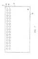
- FIG. 1is an elevation view of module 10 devised in accordance with a preferred embodiment of the present invention.
- FIG. 2is an elevation view of module 10 devised in accordance with a preferred embodiment of the present invention.
- FIG. 3depicts, in enlarged view, the area marked “A” in FIG. 2 .
- FIG. 4is an enlarged detail of an exemplar connection in a preferred embodiment of the present invention.
- FIG. 5is an enlarged depiction of an exemplar area around a lower flex contact in a preferred embodiment of the present invention.
- FIG. 6depicts a first outer surface layer of a flex circuit employed in a preferred embodiment of the present invention.
- FIG. 7depicts a first outer surface layer of a flex circuit employed in a preferred embodiment of the present invention.
- FIG. 8depicts a first conductive layer of a flex circuit employed in a preferred embodiment of the present invention.
- FIG. 9illustrates a first conductive layer of a flex circuit employed in a preferred embodiment of the present invention.
- FIG. 10depicts an intermediate layer of a flex circuit employed in a preferred embodiment of the present invention.
- FIG. 11depicts an intermediate layer of a right side flex circuit employed in a preferred embodiment of the present invention.
- FIG. 12depicts a second conductive layer of a flex circuit of a preferred embodiment of the present invention.
- FIG. 13depicts a second conductive layer of a flex circuit of a preferred embodiment of the present invention.
- FIG. 14depicts a second outer layer of a flex circuit employed in a preferred embodiment of the present invention.
- FIG. 15reflects a second outer layer of a flex circuit employed in a preferred embodiment of the present invention.
- FIG. 16depicts an alternative preferred embodiment of the present invention.
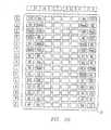
- FIG. 17illustrates a JEDEC pinout for DDR-II FBGA packages.
- FIG. 18illustrates the pinout of a module 10 in an alternative preferred embodiment of the invention.
- FIG. 19illustrates the pinout of a module 10 in an alternative embodiment of the invention.
- FIG. 20depicts the pinout of an exemplar CSP employed in a preferred embodiment of the invention.
- FIG. 21depicts a second conductive layer of a flex circuit employed in an alternative preferred embodiment of the present invention.
- FIG. 22depicts a second conductive layer of a flex circuit employed in an alternative preferred embodiment of the present invention.
- FIG. 23is an elevation view of a precursor assembly devised in accordance with a preferred embodiment of the present invention comprising stiffeners.
- FIG. 23Adepicts, in enlarged view, the area marked “ 23 A” in FIG. 23 .
- FIG. 24is a plan view of stiffener stock devised in accordance with a preferred embodiment of the present invention.
- FIG. 25depicts, in enlarged view, the area marked “ 25 ” in FIG. 24 .
- FIG. 26is a perspective view of a panel or strip comprising flex circuits devised in accordance with a preferred embodiment of the present invention with stiffener stock attached.
- FIG. 27is a plan view of a panel or strip comprising flex circuits devised in accordance with a preferred embodiment of the present invention with stiffener stock attached.
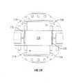
- FIG. 28depicts, in enlarged view, the area marked “ 28 ” in FIG. 24 .
- FIG. 29depicts a CSP placed on a flex circuit in accordance with a preferred embodiment of the present invention.
- FIG. 30presents another depiction of a CSP placed on a flex circuit in accordance with a preferred embodiment of the present invention.
- FIG. 31depicts two flex circuit edges in an arrangement according to a preferred embodiment of the present invention.
- FIG. 32depicts two flex edges in accordance with an alternative preferred embodiment of the present invention.
- FIG. 33is a plan view from below of a precursor assembly devised in accordance with a preferred embodiment of the present invention.
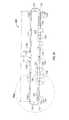
- FIG. 34is an elevation view of a stacked circuit module devised in accordance with a preferred embodiment of the present invention.
- FIG. 35is an elevation view of a stacked circuit module devised in accordance with another preferred embodiment of the present invention.
- FIG. 36is a perspective view from below of a stacked circuit module devised in accordance with a preferred embodiment of the present invention.
- FIG. 37is a perspective view from above of a stacked circuit module devised in accordance with a preferred embodiment of the present invention.
- FIG. 38is an elevation view of a stacked circuit module devised in accordance, with another preferred embodiment of the present invention.
- FIG. 39depicts a tooling apparatus devised in accordance with a preferred embodiment of the present invention.
- FIG. 40depicts an enlarged depiction of the area marked “ 40 ” in FIG. 39 .
- FIG. 41illustrates a tooling apparatus in accordance with a preferred embodiment of the present invention.
- FIG. 42illustrates another step in devising an assembly in accordance with a preferred embodiment of the present invention.
- FIG. 43depicts another step in devising an assembly in accordance with a preferred embodiment of the present invention.
- FIG. 44depicts a tooling apparatus devised in accordance with another preferred embodiment of the present invention, and illustrates a step in accordance with another preferred embodiment of the present invention.
- FIG. 45illustrates another step in devising an assembly in accordance with another preferred embodiment of the present invention.
- FIG. 46depicts another step in devising an assembly in accordance with another preferred embodiment of the present invention.
- FIG. 47illustrates another step in devising an assembly in accordance with another preferred embodiment of the present invention.
- FIG. 48depicts another step in devising an assembly in accordance with another preferred embodiment of the present invention.
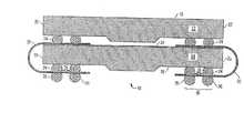
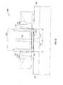
- FIG. 1is an elevation view of module 10 devised in accordance with a preferred embodiment of the present invention.
- Module 10is comprised of upper CSP 12 and lower CSP 14 .
- Each of CSPs 12 and 14have an upper surface 16 and a lower surface 18 and opposite lateral sides 20 and 22 .
- CSPschip scale packaged integrated circuits
- FIGS. 1 and 2are depicted with CSPs of a particular profile known to those in the art, but it should be understood that the figures are exemplary only.
- CSPssuch as, for example, ball-grid-array (“BGA”), micro-ball-grid array (“ ⁇ BGA”), and fine-pitch ball grid array (“FBGA”) packages have an array of connective contacts embodied, for example, as leads, bumps, solder balls, or balls that extend from lower surface 18 of a plastic casing in any of several patterns and pitches. An external portion of the connective contacts is often finished with a ball of solder. Shown in FIG. 1 are CSP contacts 24 along lower surfaces 18 of CSPs 12 and 14 . CSP contacts 24 provide connection to the integrated circuit within the respective packages. Collectively, CSP contacts 24 comprise CSP array 26 shown as to lower CSP 14 in the depicted particular package configuration as CSP arrays 26 1 and 26 2 which collectively comprise CSP array 26 .
- BGAball-grid-array
- ⁇ BGAmicro-ball-grid array
- FBGAfine-pitch ball grid array
- flex circuits(“flex”, “flex circuits” or “flexible circuit structures”) 30 and 32 are shown partially wrapped about lower CSP 14 with flex 30 partially wrapped over lateral side 20 of lower CSP 14 and flex 32 partially wrapped about lateral side 22 of lower CSP 14 .
- Lateral sides 20 and 22may be in the character of sides or may, if the CSP is especially thin, be in the character of an edge. Any flexible or conformable substrate with a multiple internal layer connectivity capability may be used as a flex circuit in the invention.
- the entire flex circuitmay be flexible or, as those of skill in the art will recognize, a PCB structure made flexible in certain areas to allow conformability around lower CSP 14 and rigid in other areas for planarity along CSP surfaces may be employed as an alternative flex circuit in the present invention.
- structures known as rigid-flexmay be employed.
- Portions of flex circuits 30 and 32are fixed to upper surface 16 of lower CSP 14 by adhesive 34 which is shown as a tape adhesive, but may be a liquid adhesive or may be placed in discrete locations across the package.
- adhesive 34is thermally conductive. Adhesives that include a flux are used to advantage in assembly of module 10 .
- Layer 34may also be a thermally conductive medium to encourage heat flow between the CSPs of module 10 .
- Flex circuits 30 and 32are multi-layer flexible circuit structures that have at least two conductive layers.
- the conductive layersare metal such as alloy 110 .
- the use of plural conductive layersprovides advantages as will be seen and the creation of a distributed capacitance across module 10 intended to reduce noise or bounce effects that can, particularly at higher frequencies, degrade signal integrity, as those of skill in the art will recognize.
- Module 10 of FIG. 1has module contacts 36 collectively identified as module array 38 .
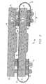
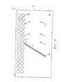
- FIG. 2shows a module 10 devised in accordance with a preferred embodiment of the invention.
- FIG. 2illustrates use of a conformal media 40 provided in a preferred embodiment to assist in creating conformality of structural areas of module 10 .
- Planarity of the moduleis improved by conformal media 40 .
- conformal media 40is thermally conductive.
- thermal spreaders or a thermal mediummay be placed as shown by reference 41 .
- Identified in FIG. 2are upper flex contacts 42 and lower flex contacts 44 that are at one of the conductive layers of flex circuits 30 and 32 .
- Upper flex contacts 42 and lower flex contacts 44are conductive material and, preferably, are solid metal.
- Lower flex contacts 44are collectively lower flex contact array 46 .
- Upper flex contacts 42are collectively upper flex contact array 48 . Only some of upper flex contacts 42 and lower flex contacts 44 are identified in FIG. 2 to preserve clarity of the view. It should be understood that each of flex circuits 30 and 32 have both upper flex contacts 42 and lower flex contacts 44 . Lower flex contacts 44 are employed with lower CSP 14 and upper flex contacts 42 are employed with upper CSP 12 .
- FIG. 2has an area marked “A” that is subsequently shown in enlarged depiction in FIG. 3 .
- FIG. 3depicts in enlarged view, the area marked “A” in FIG. 2 .
- FIG. 3illustrates the connection between example CSP contact 24 and module contact 36 through lower flex contact 44 to illustrate the solid metal path from lower CSP 14 to module contact 36 and, therefore, to an application PWB to which module is connectable. As those of skill in the art will understand, heat transference from module 10 is thereby encouraged.
- CSP contact 24 and module contact 36together offset module 10 from an application platform such as a PWB.
- the combined heights of CSP contact 24 and module contact 36provide a moment arm longer than the height of a single CSP contact 24 alone. This provides a longer moment arm through which temperature-gradient-over-time stresses (such as typified by temp cycle), can be distributed.
- Flex 30is shown in FIG. 3 to be comprised of multiple layers. Flex 30 has a first outer surface 50 and a second outer surface 52 . Flex circuit 30 has at least two conductive layers interior to first and second outer surfaces 50 and 52 . There may be more than two conductive layers in flex 30 and flex 32 . In the depicted preferred embodiment, first conductive layer 54 and second conductive layer 58 are interior to first and second outer surfaces 50 and 52 . Intermediate layer 56 lies between first conductive layer 54 and second conductive layer 58 . There may be more than one intermediate layer, but one intermediate layer of polyimide is preferred.
- lower flex contact 44is preferably comprised from metal at the level of second conductive layer 58 interior to second outer surface 52 .
- Lower flex contact 44is solid metal in a preferred embodiment and is comprised of metal alloy such as alloy 110 . This results in a solid metal pathway from lower CSP 14 to an application board thereby providing a significant thermal pathway for dissipation of heat generated in module 10 .
- FIG. 4is an enlarged detail of an exemplar connection between example CSP contact 24 and example module contact 36 through lower flex contact 44 to illustrate the solid metal path from lower CSP 14 to module contact 36 and, therefore, to an application PWB to which module 10 is connectable.
- lower flex contact 44is at second conductive layer 58 that is interior to first and second outer surface layers 50 and 52 respectively, of flex circuit 30 .
- FIG. 5is an enlarged depiction of an exemplar area around a lower flex contact 44 in a preferred embodiment.
- Windows 60 and 62are opened in first and second outer surface layers 50 and 52 respectively, to provide access to particular lower flex contacts 44 residing at the level of second conductive layer 58 in the flex.
- the upper flex contacts 42are contacted by CSP contacts 24 of upper CSP 12 .
- Lower flex contacts 44 and upper flex contacts 42are particular areas of conductive material (preferably metal such as alloy 110 ) at the level of second conductive layer 58 in the flex.
- Upper flex contacts 42 and lower flex contacts 44are demarked in second conductive layer 58 and, as will be shown in subsequent Figs., may be connected to or isolated from the conductive plane of second conductive layer 58 .
- Demarking a lower flex contact 44 from second conductive layer 58is represented in FIG. 5 by demarcation gap 63 shown at second conductive layer 58 .
- demarcation gapsdo not extend completely around the flex contact as shown, for example, by lower flex contacts 44 C in later FIG. 12 .
- CSP contacts 24 of lower CSP 14pass through a window 60 opened through first outer surface layer 50 , first conductive layer 54 , and intermediate layer 56 , to contact an appropriate lower flex contact 44 .
- Window 62is opened through second outer surface layer 52 through which module contacts 36 pass to contact the appropriate lower flex contact 44 .
- Respective ones of CSP contacts 24 of upper CSP 12 and lower CSP 14are connected at the second conductive layer 58 level in flex circuits 30 and 32 to interconnect appropriate signal and voltage contacts of the two CSPs.
- Respective CSP contacts 24 of upper CSP 12 and lower CSP 14 that convey ground (VSS) signalsare connected at the first conductive layer 54 level in flex circuits 30 and 32 by vias that pass through intermediate layer 56 to connect the levels as will subsequently be described in further detail.
- CSPs 12 and 14are connected. Consequently, when flex circuits 30 and 32 are in place about lower CSP 14 , respective CSP contacts 24 of each of upper and lower CSPs 12 and 14 are in contact with upper and lower flex contacts 42 and 44 , respectively. Selected ones of upper flex contacts 42 and lower flex contacts 44 are connected. Consequently, by being in contact with lower flex contacts 44 , module contacts 36 are in contact with both upper and lower CSPs 12 and 14 .
- module contacts 36pass through windows 62 opened in second outer layer 52 to contact lower flex contacts 44 .
- module 10will exhibit a module contact array 38 that has a greater number of contacts than do the constituent CSPs of module 10 .
- some of module contacts 36may contact lower flex contacts 44 that do not contact one of the CSP contacts 24 of lower CSP 14 but are connected to CSP contacts 24 of upper CSP 12 . This allows module 10 to express a wider datapath than that expressed by the constituent CSPs 12 or 14 .
- a module contact 36may also be in contact with a lower flex contact 44 to provide a location through which different levels of CSPs in the module may be enabled when no unused CSP contacts are available or convenient for that purpose.
- first conductive layer 54is employed as a ground plane, while second conductive layer 58 provides the functions of being a signal conduction layer and a voltage conduction layer.
- first and second conductive layersmay be reversed with attendant changes in windowing and use of commensurate interconnections.
- first and second conductive layers 54 and 58there is at least one intermediate layer 56 that, in a preferred embodiment, is a polyimide. Placement of such an intermediate layer between ground-conductive first conductive layer 54 and signal/voltage conductive second conductive layer 58 provides, in the combination, a distributed capacitance that assists in mitigation of ground bounce phenomena to improve high frequency performance of module 10 .
- FIG. 6depicts first outer surface layer 50 of flex 30 (i.e., left side of FIG. 1 ). The view is from above the flex looking down into flex 30 from the perspective of first conductive layer 54 . Throughout the Figs., the location reference “B” is to orient views of layers of flex 30 to those of flex 32 as well as across layers. Windows 60 are opened through first outer surface layer 50 , first conductive layer 54 , and intermediate layer 56 . CSP contacts 24 of lower CSP 14 pass through windows 60 of first outer surface layer 50 , first conductive layer 54 , and intermediate layer 56 to reach the level of second conductive layer 58 of flex 30 .
- selected CSP contacts 24 of lower CSP 14make contact with selected lower flex contacts 44 .
- Lower flex contacts 44provide several types of connection in a preferred embodiment as will be explained with reference to later FIG. 12 .
- a portion of flex 30will be wrapped about lateral side 20 of lower CSP 14 to place edge 62 above upper surface 16 of lower CSP 14 .
- FIG. 7depicts first outer surface layer 50 of flex 32 (i.e., right side of FIG. 1 ).
- the viewis from above the flex looking down into flex 32 from the perspective of first conductive layer 54 .
- the location reference “B”relatively orients the views of FIGS. 6 and 7 .
- the views of FIGS. 6 and 7may be understood together with the reference marks “B” of each view being placed nearer each other than to any other corner of the other view of the pair of views of the same layer.
- windows 60are opened through first outer surface layer 50 , first conductive layer 54 and intermediate layer 56 .
- CSP contacts 24 of lower CSP 14pass through windows 60 of first outer surface layer 50 , first conductive layer 54 , and intermediate layer 56 to reach the level of second conductive layer 58 of flex 30 .
- selected CSP contacts 24 of lower CSP 14make contact with lower flex contacts 44 .
- Lower flex contacts 44provide several types of connection in a preferred embodiment as will be explained with reference to later FIG. 12 .
- FIG. 8depicts first conductive layer 54 of flex 30 .
- Windows 60continue the opened orifice in flex 30 through which CSP contacts 24 of lower CSP 14 pass to reach second conductive layer 58 and, therefore, selected lower flex contacts 44 at the level of second conductive layer 58 .
- first conductive layer 54becomes, on the part of flex 30 disposed above upper surface 16 of lower CSP 14 , the lower most conductive layer of flex 30 from the perspective of upper CSP 12 .
- those CSP contacts 24 of upper CSP 12 that provide ground (VSS) connectionsare connected to the first conductive layer 54 .
- First conductive layer 54lies beneath, however, second conductive layer 58 in that part of flex 30 that is wrapped above lower CSP 14 . Consequently, some means must be provided for connection of the upper flex contact 42 to which ground-conveying CSP contacts 24 of upper CSP 12 are connected and first conductive layer 54 .
- those upper flex contacts 42 that are in contact with ground-conveying CSP contacts 24 of upper CSP 12have vias that route through intermediate layer 56 to reach first conductive layer 54 .
- the sites where those vias meet first conductive layer 54are identified in FIG. 8 as vias 66 .
- These viasmay be “on-pad” or coincident with the flex contact 42 to which they are connected.
- vias 66 in FIG. 8are one via.
- vias in the figuresare shown larger in diameter than in manufactured embodiments.
- connection between conductive layers provided by viasmay be provided any of several well-known techniques such as plated holes or solid lines or wires and need not literally be vias.
- Off-pad vias 74are disposed on first conductive layer 54 at locations near, but not coincident with selected ones of windows 60 . Unlike vias 66 that connect selected ones of upper flex contacts 42 to first conductive layer 54 , off-pad vias 74 connect selected ones of lower flex contacts 44 to first conductive layer 54 . In the vicinity of upper flex contacts 42 , second conductive layer 58 is between the CSP connected to module 10 by the upper flex contacts 42 (i.e., upper CSP 12 ) and first conductive layer 54 .
- first conductive layer 54is between the CSP connected to module 10 by the lower flex contacts 44 (i.e., lower CSP 14 ) and second conductive layer 58 . Consequently, vias between ground-conveying lower flex contacts 44 and first conductive layer 54 are offset from the selected lower flex contacts 44 by off-pad vias 74 shown in offset locations.
- FIG. 9illustrates first conductive layer 54 of flex 32 .
- the location reference marks “B”are employed to relatively orient FIGS. 8 and 9 .
- Windows 60 , vias 66 and off-pad vias 74are identified in FIG. 9 .
- Enable via 70is connected off-pad to a selected lower flex contact 44 that corresponds, in this preferred embodiment, to an unused CSP contact 24 of lower CSP 14 (i.e., a N/C).
- a module contact 36 at that siteconveys an enable signal (C/S) for upper CSP 12 through the selected lower flex contact 44 (which is at the level of second conductive layer 58 ) to off-pad enable via 70 that conveys the enable signal to first conductive layer 54 and thereby to enable trace 72 .
- Enable trace 72further conveys the enable signal to enable via 68 which extends through intermediate layer 56 to selected upper flex contact 42 at the level of second conductive layer 58 where contact is made with the C/S pin of upper CSP 12 .
- upper and lower CSPs 12 and 14may be independently enabled.
- FIG. 10depicts intermediate layer 56 of flex 30 .
- Windows 60are shown opened in intermediate surface 56 .
- CSP contacts 24 of lower CSP 14pass through windows 60 in intermediate layer 58 to reach lower flex contacts 44 at the level of second conductive layer 58 .
- windows 60narrow in diameter from their manifestation in first outer layer 50 .
- Vias 66 , off-pad vias 74 , and enable vias 68 and 70pass through intermediate layer 56 connecting selected conductive areas at the level of first and second conductive layers 54 and 58 , respectively.
- FIG. 11depicts intermediate layer 56 of flex 32 showing windows 60 , vias 66 , off-pad vias 74 , and enable vias 68 and 70 passing through intermediate layer 56 .
- FIG. 12depicts second conductive layer 58 of flex 30 of a preferred embodiment of the present invention. Depicted are various types of upper flex contacts 42 , various types of lower flex contacts 44 , signal traces 76 , and VDD plane 78 as well as previously described vias 66 and off-pad vias 74 . Throughout FIGS. 12 and 13 , only exemplars of particular features are identified to preserve clarity of the view. Flex contacts 44 A are connected to corresponding selected upper flex contacts 42 A with signal traces 76 . To enhance the clarity of the view, only exemplar individual flex contacts 44 A and 42 A are literally identified in FIG. 12 .
- signal traces 76exhibit path routes determined to provide substantially equal signal lengths between corresponding flex contacts 42 A and 44 A. As shown, traces 76 are separated from the larger surface area of second conductive layer 58 that is identified as VDD plane 78 . VDD plane 78 may be in one or more delineated sections but, preferably is one section. Lower flex contacts 44 C provide connection to VDD plane 78 . In a preferred embodiment, upper flex contacts 42 C and lower flex contacts 44 C connect upper CSP 12 and lower CSP 14 , respectively, to VDD plane 78 . Lower flex contacts 44 that are connected to first conductive layer 54 by off-pad vias 74 are identified as lower flex contacts 44 B. To enhance the clarity of the view, only exemplar individual lower flex contacts 44 B are literally identified in FIG. 12 . Upper flex contacts 42 that are connected to first conductive layer 54 by vias 66 are identified as upper flex contacts 42 B.
- FIG. 13depicts second conductive layer 58 of right side flex 32 of a preferred embodiment of the present invention. Depicted are various types of upper flex contacts 42 , various types of lower flex contacts 44 , signal traces 76 , and VDD plane 78 as well as previously described vias 66 , off-pad vias 74 , and enable vias 70 and 68 .
- FIG. 13illustrates upper flex contacts 42 A connected by traces 76 to lower flex contacts 44 A.
- VDD plane 78provides a voltage plane at the level of second conductive layer 58 .
- Lower flex contacts 44 C and upper flex contacts 42 Cconnect lower CSP 14 and upper CSP 12 , respectively, to VDD plane 78 .
- Lower flex contact 44 Dis shown with enable via 70 described earlier.
- Corresponding upper flex contact 42 Dis connected to lower flex contact 44 D through enable vias 70 and 68 that are connected to each other through earlier described enable trace 72 at the first conductive layer 54 level of flex 32 .
- FIG. 14depicts second outer layer 52 of flex 30 .
- Windows 62are identified. Those of skill will recognize that module contacts 36 pass through windows 62 to contact appropriate lower flex contacts 44 .
- flex 30is partially wrapped about lateral side 20 of lower CSP 14 , a portion of second outer layer 52 becomes the upper-most layer of flex 30 from the perspective of upper CSP 12 .
- CSP contacts 24 of upper CSP 12pass through windows 64 to reach second conductive layer 58 and make contact with appropriate ones of upper flex contacts 42 located at that level.
- FIG. 15reflects second outer layer 52 of flex 32 and exhibits windows 64 and 62 .
- Module contacts 36pass through windows 62 to contact appropriate lower flex contacts 44 .
- CSP contacts 24 of upper CSP 12pass through windows 64 to reach second conductive layer 58 and make contact with appropriate ones of upper flex contacts 42 located at that level.
- FIG. 16depicts an alternative preferred embodiment of the present invention showing module 10 .
- module contacts 36 Esupply a part of the datapath of module 10 and may provide a facility for differential enablement of the constituent CSPs.
- a module contact 36 E not employed in wide datapath provisionmay provide a contact point to supply an enable signal to differentially enable upper CSP 12 or lower CSP 14 .
- a wide datapath module 10the data paths of the constituent upper CSP 12 and lower CSP 14 are combined to provide a module 10 that expresses a module datapath that is twice the width of the datapaths of the constituent CSPs in a two-high module 10 .
- the preferred method of combinationis concatenation, but other combinations may be employed to combine the datapaths of CSPs 12 and 14 on the array of module contacts 36 and 36 E.
- FIGS. 17, 18 , and 19are provided to illustrate using added module contacts 36 E in alternative embodiments of the present invention to provide wider datapaths for module 10 than are present in constituent CSPs 12 and 14 .
- FIG. 17illustrates a JEDEC pinout for DDR-II FBGA packages.
- FIG. 18illustrates the pinout provided by module contacts 36 and 36 E of a module 10 expressing an 8-bit wide datapath.
- Module 10is devised in accordance with the present invention and is, in the exemplar embodiment, comprised of an upper CSP 12 and lower CSP 14 that are DDR-II-compliant in timing, but each of which are only 4 bits wide in datapath. As will be recognized, the module 10 mapped in FIG.
- FIG. 18expresses an 8-bit wide datapath.
- FIG. 18depicts DQ pins differentiated in source between upper CSP 12 (“top”) and lower CSP 14 (“bot”) to aggregate to 8-bits.
- FIG. 19illustrates the pinout provided by module contacts 36 and 36 E of module 10 expressing a 16-bit wide datapath.
- Module 10is devised in accordance with the present invention and is, in this exemplar embodiment, comprised of an upper CSP 12 and lower CSP 14 that are DDR-II-compliant in timing, but each of which are only 8-bits wide in datapath.
- the wide datapath embodimentmay be employed with any of a variety of CSPs available in the field and such CSPs need not be DDR compliant.
- FIG. 20illustrates a typical pinout of a memory circuit provided as a CSP and useable in the present invention. Individual array positions are identified by the JEDEC convention of numbered columns and alphabetic rows. The central area (e.g., A3-A6; B3-B6; etc.) is unpopulated. CSP contacts 24 are present at the locations that are identified by alpha-numeric identifiers such as, for example, A3, shown as an example CSP contact 24 .
- FIG. 21depicts second metal layer 58 of flex 30 in an alternative embodiment of the invention in which module 10 expresses a datapath wider than that expressed by either of the constituent CSPs 12 and 14 .
- Lower flex contacts 44 Eare not contacted by CSP contacts 24 of lower CSP 14 , but are contacted by module contacts 36 E to provide, with selected module contacts 36 , a datapath for module 10 that is 2n-bits in width where the datapaths of CSPs 12 and 14 have a width of n-bits.
- lower flex contacts 44 Eare connected to upper flex contacts 42 E.
- windows 62pass through second outer layer 52 .
- module contacts 36 and 36 Epass through windows 62 in second outer layer 52 of flex circuit 30 , to contact appropriate lower flex contacts 44 .
- FIG. 22illustrates second metal layer 58 of flex 32 in an alternative embodiment of the invention in which module 10 expresses a datapath wider than that expressed by either of the constituent CSPs 12 and 14 .
- Lower flex contacts 44 Eare not contacted by CSP contacts 24 of lower CSP 14 , but are contacted by module contacts 36 E to provide, with selected module contacts 36 , a datapath for module 10 that is 2n-bits in width where the datapaths of CSPs 12 and 14 have a width of n-bits.
- lower flex contacts 44 Eare connected to upper flex contacts 42 E.
- windows 62pass through second outer layer 52 .
- module contacts 36pass through windows 62 in second outer layer 52 of flex circuit 32 , to contact appropriate lower flex contacts 44 .
- module contacts 36 Econtact flex contacts 44 E and 44 EE.
- lower flex contacts 44 Eare, in the depicted embodiment, eight (8) in number and that there is another lower flex contacts identified by reference 44 EE shown on FIG. 21 .
- Lower flex contact 44 EEis contacted by one of the module contacts 36 E to provide differential enablement between upper and lower CSPs.
- lower flex contacts 44 Eare connected to corresponding upper flex contacts 42 E.
- CSP contacts 24 of upper CSP 12 that convey dataare in contact with upper flex contacts 42 E.
- module 10expresses a 16-bit datapath and CSP 12 and CSP 14 each express an 8-bit datapath.
- FIGS. 23-33depict aspects of alternative preferred embodiments of a precursor assembly for use as a component of a stacked circuit module.
- FIGS. 23-33depict aspects of stiffeners comprised in exemplary precursor assemblies and additional aspects of other components used in manufacturing such precursor assemblies.
- FIG. 23is an elevation view of an end of precursor assembly 105 comprising CSP 114 having an upper surface 116 , a lower surface 118 , and opposite lateral sides 120 and 122 .
- CSP 114Upon assembly of a stacked circuit module 110 using precursor assembly 105 of this embodiment, CSP 114 will become a lower CSP of a stacked circuit module 110 .
- CSPsthat are useful for CSP 114 are the types that include at least one integrated circuit or semiconductor chip surrounded by a package body 127 with a lateral extent L defined by the opposite lateral edges or sides 120 and 122 .
- the package body surrounding the integrated circuit(s) or semiconductor chip(s)need not be plastic, but a large majority of package bodies in CSP technologies are plastic.
- the package bodyneed not surround the integrated circuit(s) or semiconductor chip(s) completely, leaving one or more sides, edges, surfaces, or other regions of the integrated circuit(s) or semiconductor chip(s) exposed, but a large majority of package bodies in CSP technologies completely encase the integrated circuit(s) or semiconductor chip(s) or leave only the terminals on integrated circuit or semiconductor chip active face(s) exposed.
- the inventionmay also be used with those CSP-like packages that exhibit bare die connectives on one major surface.
- one of the constituent CSPs of an example stacked circuit module 110may be a typical CSP having lateral edges 120 and 122 that have an appreciable height to present a “side” while other constituent CSPs of the same stacked circuit module 110 may be devised in packages that have lateral edges 120 and 122 that are more in the character of an edge rather than a side having appreciable height. All devices such as those discussed above and similar devices are included within the meaning of the term CSP, which term should be broadly considered in the context of this application.
- the embodiment of a precursor assembly illustrated in FIG. 23uses substantially planar stiffeners 139 that are initially disposed on a flex circuit 130 and affixed thereto with adhesive 134 .
- stiffeners 139are disposed along a surface of CSP 114 even if literally separated from that surface, such as by adhesive 135 , for example.
- stiffeners 139are attached to CSP 114 with adhesive 135 .
- CSP contacts 124regardless of configuration, generally will define a mounting height for CSP, such as mounting height H depicted in FIG. 23A for CSP contacts comprising solder balls.
- thickness T of stiffeners 139is less than mounting height H, for example as depicted in FIG.
- stiffeners 139also are configured to provide lateral clearance for the CSP arrays 126 comprising various CSP contacts 124 .
- CSP contacts 124are at least partially disposed within the volume 140 between stiffeners 139 .
- Stiffeners 139may take several useful configurations, but in preferred embodiments herein, stiffeners 139 are substantially planar. A preferred embodiment is shown using stiffeners 139 disposed within the lateral extent L of CSP 114 . Other embodiments may have stiffeners 139 disposed at least partially outside lateral extent L of CSP 114 , one example of which is the embodiments further discussed below in connection with FIG. 38 .
- flex circuit 130has upper portions 130 U that terminate in edges 170 A and 170 B which are separated by gap G above the upper surface 116 of CSP 114 .
- gap Gis preselected and imposed when precursor assembly 105 is made.
- Upper portions 130 U of flex circuit 130are disposed along the upper surface 116 of CSP 114 even if literally separated from that surface, such as by adhesive 171 , for example. In such configurations, flex circuit 130 has a folded portion 131 .
- FIG. 23depicts precursor assembly 105 with module contacts 136 through which the precursor assembly 105 may connect to an application environment or to another precursor assembly 105 , for example, as shown in FIG. 34 .
- the module, contacts 136are deployed in a module contact array 138 , but other configurations of module contacts may be used.
- module contacts 136 in the form of the depicted solder ballsare not required to connect a stacked circuit module 110 to an application environment or to connect a precursor assembly 105 to another precursor assembly 105 , and that other connective strategies may be employed such as, for example, direct pad to pad connection schemes or connective structures other than solder balls.
- a preferred method for practicing the inventionproduces precursor assemblies 105 in batches of six.
- the stiffener(s) and flex circuit(s) for a particular precursor assemblyare provided in aggregation with other stiffeners and flex circuits, respectively, for other precursor assemblies.
- FIG. 24depicts an exemplar strip or panel of stiffener stock 237 that may be employed in some preferred embodiments of the present invention
- FIG. 25depicts an enlarged depiction of the area marked “ 25 ” in FIG. 24 .
- the illustrated strip of stiffener stock 237includes twelve stiffeners 139 retained by tabs 238 in configuration for deployment in six precursor assemblies 105 .
- the stiffener materialhas cutouts comprising tooling holes 239 and windows 240 .
- Windows 240are configured to accommodate CSP arrays 126 comprising CSP contacts 124 of CSP 114 .
- tabs 238 A and tooling holes 239 Aare disposed generally as half of a tab 238 and a tooling hole 239 as disposed between adjacent windows 240 .
- Stiffener stock 237 as depicted in the embodiment of FIG. 24comprises a polymer having thermal properties adequate for the various temperatures at which various solder reflow and other attachment operations may occur in the production of precursor assemblies 105 and stacked circuit modules 110 and in the deployment of stacked circuit modules 110 in an application environment.
- stiffener stock 237comprises a single layer or multiple laminated layers of polyimide film selected so that stiffeners 139 have mechanical properties compatible with the mechanical properties of flex circuit 130 , but other materials that are compatible with the assembly processes may be used such as resin polymer matrix composites, engineering ceramics or ceramic fibers, graphite composites, or filled and non-filled plastics known to those of skill in the art.
- stiffener stock 237also may take other configurations and compositions and may, for example, be devised in more than one piece and/or be devised of material that is thermally conductive.
- stiffener stock 237may comprise material of sufficient rigidity such as stainless steels, aluminum, copper, or other metals or metal alloys so that stiffeners 139 control the coplanarity of CSP 114 by inhibiting warping.
- FIGS. 26 and 27depict perspective and plan views, respectively, of stiffener stock 237 disposed on a panel or strip 230 comprising flex circuits 130 .
- six flex circuits 130are configured side-by-side, with a portion of each flex circuit 130 accessible through a respective window 240 of stiffener stock 237 .
- Strip 230further comprises lateral edges 231 and strip edge portions 232 .
- an adhesive 134(shown earlier) is used to attach stiffener stock 237 and its component stiffeners 139 and tabs 238 to strip or panel 230 and its component flex circuits 130 .
- Adhesive 134in a preferred embodiment comprises a dry film adhesive.
- adhesive 134may be selectively applied to selected portions of stiffener stock 237 or strip 230 , or both, and that other methods for attaching stiffeners 139 to flex circuits 130 may be employed in accordance with various embodiments of the present invention including, for example, laminate tape adhesive, liquid adhesive, and ultrasonic or thermal bonding.
- the adhesivewill be thermally conductive.
- tooling holes 239facilitate alignment of stiffener stock 237 and strip 230 , although alternative methods such as machine vision aided pick & place may be employed.
- FIG. 28depicts an enlarged depiction of the area marked “ 28 ” in FIG. 27 .
- the depiction of FIG. 28is centered on a site where a CSP 114 will be disposed.
- selected CSP contacts 124will be connected to respective ones of flex contacts disposed in flex contact arrays.
- the depiction of FIG. 28shows through window 240 only selected ones of flex contacts 144 of a selected flex contact array 146 .
- Components of stiffener stock 237 relevant to the illustrated siteinclude stiffeners 139 , tabs 238 , tooling holes 239 , and window 240 .
- the portion of strip 230 depicted in FIG. 28also illustrates various features of flex circuit 130 of a preferred embodiment.
- a singulation opening 233is disposed through strip 230 adjacent to each longitudinal end of each stiffener 139 .
- Additional singulation openings 234are disposed through strip 230 along strip edge portions 232 adjacent to each lateral edge 231 of strip 230 .
- Edges 170 A and 170 B of upper portions 130 U of flex circuit 130are disposed along singulation openings 234 , with each upper portion 130 U disposed between a respective singulation opening 234 and a respective stiffener 139 .
- Strip 230 and the flex circuits 130 disposed thereoncan be configured with conductive components in a wide variety of ways.
- strip 230 and the flex circuits 130 disposed thereoncan be multi-layer flexible circuit structures, such as the embodiment discussed above having a first conductive layer and a second conductive layer that are interior to first and second outer surfaces, with an intermediate layer disposed between the first conductive layer and the second conductive layer.
- a single conductive layer or three or more conductive layerscan also be used, and typically the choice will depend on the complexity of the circuit routing required.
- some embodimentsmay employ only one cover coat, such as those instances in which a ground plane is exposed.
- Circuit tracescan be disposed in one or more conductive layers, and selected conductive layers may contain only ground or voltage planes.
- conductive tracesare disposed at one conductive layer with a ground plane disposed an another conductive layer.
- a single outer surfaceis used leaving one of the conductive layers exposed. All contact pads on the exposed conductive layer are connected to the other conductive surface through vias, using no conductive traces on the exposed conductive layer. Connecting the contact pads directly through vias mitigates solder wicking and reduces costs and thickness of the flex circuitry.
- strip 230may employ various electroplating steps that use current supplied from sprocket rails engaging sprocket holes 235 .
- Current for electroplatingcan be routed along bussing through trim tabs 250 , which are severed from flex circuits 130 during singulation as discussed further below.
- Electroplating bus pathsalso can converge at various connection points of strip 230 , which bussing connections can be severed following electroplating by making de-bussing punches 251 as illustrated in FIG. 28 .
- other methodsmay be used to dispose conductive material within and/or on strip 230 .
- nonbussed portion 150 of flex circuit 130is disposed alongside tab 238 and between singulation openings 233 to provide additional clearance for circuitry of flex circuit 130 during singulation, as discussed further below.
- FIG. 28also depicts the various pattern recognition marks, or “fiducials,” used by automated assembly equipment during manufacture: of precursor assemblies 105 .
- fiducialsare metal defined, asymmetrically placed, and comprise a cross and a square where practical.
- the preferred embodiment depictedhas global fiducials 260 defined by circular metal regions on the surface of strip 230 and aligned with tooling holes 239 .
- Additional global fiducialsare defined by metal regions in the form of a square (fiducials 261 ) and a cross (fiducials 262 ).
- the global fiducialsare used as reference points during singulation of precursor assemblies 105 or stacked circuit modules 110 .
- local fiducialsdefined by metal regions in the form of a square (fiducials 161 ) and a cross (fiducials 162 ) defined in a conductive layer of the flex circuit, which local fiducials are used by automated equipment as a reference during the placement of CSP 114 on flex circuit 130 .
- FIG. 28Although the description of the embodiment illustrated in FIG. 28 is directed to features related to a single precursor assembly 105 to be made using stiffener stock 237 and strip 230 , those of skill will recognize that the described features can be replicated for other precursor assemblies 105 or that variations in the described features can be employed for other precursor assemblies 105 .
- adhesive 135Prior to placement of CSP 114 on flex circuit 130 , in the disclosed embodiment adhesive 135 is applied to the exposed upper surface of stiffener 139 .
- adhesive 135comprises a liquid adhesive.
- adhesive 135may be selectively applied to selected portions of stiffener 139 and that other methods for attaching stiffeners 139 to CSP 114 may be employed in various embodiments of the present invention including, for example, laminate tape adhesive and dry film adhesive.
- the adhesivewill be thermally conductive.
- Automated pick-and-place equipmentknow in the art is used to dispose CSP 114 on flex circuit 130 in a preferred embodiment.
- the pick-and-place equipmentdips CSP contacts 124 in flux prior to placement of CSP 114 on flex circuit 130 .
- heatis supplied during a first solder reflow operation to produce a solder connection between CSP contacts 124 and flex contacts 144 .
- the combination of adhesive 134 , stiffener 139 , and adhesive 135cooperate to maintain flex circuit 130 and CSP 114 in proper position during the first solder reflow operation.
- FIG. 29depicts the position of upper flex cuts 174 , and also shows the position of singulation cuts 175 made later during singulation of precursor assemblies 105 or stacked circuit modules 110 as discussed below.
- FIG. 30depicts the configuration of flex circuit 130 , stiffeners 139 , and CSP 114 following the making of upper flex cuts 174 as shown in FIG. 29 , with such depiction bounded to the left and right by the positions where singulation cuts 175 will be made later in the assembly process.
- adhesive 171is applied to the upper surface 116 of CSP 114 , to upper portions 130 U of flex circuit 130 , or to both upper surface 116 and upper portions 130 U.
- adhesive 171comprises a dry film adhesive.
- adhesive 171may be selectively applied to selected portions of upper surface 116 or upper portions 130 U, or both, and that other methods for attaching the upper surfaces 118 to flex circuits 130 may be employed in various embodiments of the present invention including, for example, laminate tape adhesive and liquid adhesive.
- the adhesivewill be thermally conductive.
- upper portions 130 U of flex circuit 130are disposed along the upper surface 116 of CSP 114 even if literally separated from that surface, such as by adhesive 171 , for example. Disposition of upper portions 130 U of flex circuit 130 along the upper surface 116 of CSP 114 can be accomplished using a tooling apparatus 180 devised in accordance with a preferred embodiment of the present invention, as depicted in FIGS. 39-43 and discussed below.
- FIG. 31depicts flex circuit edges 170 A and 170 B in a proximal arrangement according to a preferred embodiment of the present invention.
- flex circuit 130is configured for external electrical connection of lower CSP 114 .
- upper sides 133 of upper portions 130 U of flex circuit 130are depicted having upper flex contacts or pads 142 disposed in a first upper flex contact array 148 A and a second upper flex contract array 148 B.
- first upper flex contact array 148 A and second upper flex contract array 148 Bhave been abstracted to illustrate an exemplar set of upper flex contacts 142 when in practice, first upper flex contact array 148 A and second upper flex contract array 148 B may include a greater or lesser number of individual upper flex contacts or have flex contacts disposed in a different configuration, or both.
- first upper flex contact array 148 A and second upper flex contract array 148 Btogether define an array of upper flex contacts 142 configured for connection to CSP contacts 124 of upper CSP 112 .
- edges 170 A and 170 Bmay be devised to be jointly fittable with each other as shown in FIG. 32 to position first upper flex contact array 148 A and second upper flex contract array 148 B.
- Protrusion 176fits with receptive check 177 to both align laterally and transversely edges 170 A and 170 B.
- Other similar devicesmay be employed to laterally and/or transversely align edges 170 A and 170 B.
- first upper flex contact array 148 A and second upper flex contract array 148 Bare disposed in predetermined relation to each other by the jointly fittable configuration of edges 170 A and 170 B to mesh with each other. Consequently, in this depicted alternative embodiment, edges 170 A and 170 B are disposed in predetermined relation to each other by their jointly fittable configurations.
- Stacked circuit modules devised in accordance with the inventioncan comprise multiple precursor assemblies 105 as shown in FIG. 34 or a single precursor assembly 105 as shown in FIG. 35 .
- the precursor assemblies 105can be singulated at this stage with singulation cuts 175 , placed for example as depicted in FIG. 29 .
- module contacts 136are disposed along flex contacts or pads 149 on flex circuit 130 as exemplified in FIG. 33 , which depicts a plan view of an exemplar precursor assembly 105 from below.
- module contact arrays 138have been abstracted to illustrate an exemplar set of module contacts 136 when in practice, module contact arrays 138 may include a greater or lesser number of individual module contacts or module contacts disposed in a different configuration. Alternatively, in preferred embodiments singulation with singulation cuts 175 can be deferred until all precursor assemblies 105 and upper CSPs 112 have been assembled.
- FIG. 34depicts an exemplar stacked circuit module 110 in accordance with a preferred embodiment of the present invention that employs three precursor assemblies 105 .
- each flex circuit 130has folded portions 131 respective disposed adjacent to first and second lateral sides of the stack.
- stacked circuit modules 110also can be devised with one, two, three, four, or more precursor assemblies 105 , or with precursor assemblies using CSPs of different types.
- one or more lower CSPs 114may have a lateral extent L having a proportion such that folded portions 131 of one or more other precursor assemblies 110 may not be disposed outside such lateral extent.
- FIG. 35depicts an exemplar stacked circuit module 110 in accordance with a preferred embodiment of the present invention that employs a single precursor assembly 105 .
- flex circuit 130has folded portions 131 respective disposed adjacent to first and second lateral sides of the stack.
- upper CSP 112is attached to flex circuit 130 prior to singulation of stacked circuit modules 110 .
- Automated pick-and-place equipmentknow in the art is used to dispose upper CSP 112 on flex circuit 130 as shown in FIG. 35 .
- the pick-and-place equipmentdips CSP contacts 124 in flux prior to placement of CSP 112 on flex circuit 130 .
- the stacked circuit modules 110are clamped while heat is supplied during a second solder reflow operation to produce a solder connection between CSP contacts 124 and upper flex contacts 142 .
- the combination of adhesive 134 , stiffener 139 , adhesive 135 , and adhesive 171cooperate to maintain flex circuit 130 and CSP 114 in proper position during the second solder reflow operation.
- module contacts 136are disposed along flex contacts or pads 149 on flex circuit 130 in module contact arrays 138 .
- FIGS. 36 and 37depict, respectively, lower perspective and upper perspective views of an exemplar stacked circuit module 110 in accordance with a preferred embodiment of the present invention that employs a single precursor assembly 105 .
- Exemplar stacked circuit modules 110typically are connected to an application environment, such as a printed circuit board, in a third solder reflow operation.
- the combination of adhesive 134 , stiffener 139 , adhesive 135 , and adhesive 171cooperate to maintain flex circuit 130 , CSP 114 , and CSP 112 in proper position during the third solder reflow operation.
- FIG. 38depicts an exemplar stacked circuit module 110 in accordance with a preferred embodiment of the present invention that has stiffeners 139 disposed at least partially outside lateral extent L of CSP 114 .
- Embodiments as illustrated in FIG. 38may be devised when using a strip 230 and stiffener stock 237 devised for use with a CSPs having larger dimensions than CSP 114 depicted in FIG. 38 . Accordingly, in preferred embodiments, a single size of strip 230 and stiffener stock 237 can be used for a variety of CSP package sizes.
- the portions of stiffeners 139 outside lateral extent Lwill substantially control the size of gap G in many alternative methods of assembly.
- tabs 238need not be rectangular or completely trimmed away during singulation with singulation cuts 175 , but can also extend along some or all of the ends of precursor assembly 105 .
- Singulation openings 233 and upper flex cuts 174can take other shapes and be disposed in different positions, which for example provide a narrower portion of flex circuit 130 between stiffener 139 and upper surface 116 of CSP 114 to allow enhanced ventilation.
- a stabilizing fillmay be employed between flex circuit 130 and CSP 114 , for example as illustrated by conformal media 40 depicted in FIGS. 2 and 16 .
- a low profile for precursor assembly 105is provided.
- stiffener 139typically is about 0.13 mm thick
- adhesive 134is about 0.05 mm thick.
- Adhesive 135typically is about 0.07 mm thick, but can range across a variety of thicknesses. For example, in various preferred embodiments Adhesive 135 ranges from about 0.04 mm to about 0.10 mm thick. Adhesive 171 typically is about 0.08 mm thick.
- the various thicknesses used in embodiments devised in accordance with the inventionare subject to wide ranges of alternatives, as those of skill will recognize.
- FIG. 39depicts a tooling apparatus 180 devised in accordance with a preferred embodiment of the present invention illustrating the use of a physical form to set gap G between edges 170 A and 170 B of flex circuit 130 .
- Tooling apparatus 180includes a flex aligner 182 as shown in FIG. 39 used as a physical form to impose a preselected distance between the first and second edges.
- flex aligner 182When forming tool 184 disposes flex circuit 130 adjacent to upper surface 116 of CSP 114 in forming precursor assembly 105 , edges 170 A and 170 B of flex circuit 130 are limited in lateral placement along upper surface 116 of CSP 114 by flex aligner 182 .
- Gap “G”is, therefore, preselected and determined by the dimensions of flex aligner 182 when disposed between edges 170 A and 170 B. With gap G and edges 170 A and 170 B thus determined, first upper flex contact array 148 A and second upper flex contract array 148 B are positioned during assembly as exemplified in FIG. 31 .
- FIG. 40depicts an enlarged depiction of the area marked “ 40 ” in FIG. 39 .
- flex circuit 130is attached to stiffener 139 with adhesive 134 .
- precursor assembly 105comprising CSP 114 , stiffeners 139 , adhesives 134 and 135 , and flex circuit 130 is disposed in cavity 188 of jig 186 , flex circuit 130 is deflected in an upward direction as shown in FIG. 40 .
- FIG. 41illustrates a step in a method of devising an precursor assembly 105 in accordance with a preferred embodiment of the present invention.
- forming tools 184are moveable as indicated by the arrow 184 M to indicate with the “+” sign movement of forming tools 184 to dispose upper ends 130 U of flex circuit 130 over CSP 114 .
- the ends 170 A and 170 Bare set apart at distance “G” apart by flex aligner 182 .
- FIG. 42illustrates another step in a method for devising a precursor assembly 105 in accordance with a preferred embodiment of the present invention.
- Press tool 189is imposed on precursor assembly 105 after upper portions 130 U of flex circuit 130 have been disposed over the upper surface 116 of the CSP 114 and forming tools 184 are withdrawn as indicated by the arrow 184 M to indicate with the “ ⁇ ” sign movement of forming tools 184 .
- Press tool 189preferably may be heated.
- FIG. 43depicts another step in a method for devising a precursor assembly 105 in accordance with a preferred embodiment of the present invention.
- Press tool 189has moved up off of precursor assembly 105 as indicated by motion arrow 189 M.
- Flex aligner 182may now be withdrawn and precursor assembly 105 is ready for combination with either another precursor assembly 105 or a CSP 112 to form a module 110 .
- FIG. 44depicts a tooling apparatus 180 devised in accordance with another preferred embodiment of the present invention also using a physical form to set gap G between edges 170 A and 170 B of flex circuit 130 .
- jigs 186are placed in first configuration with jigs 186 set apart by a first width W 1 .
- precursor assembly 105comprising CSP 114 , stiffeners 139 , adhesives 134 and 135 , and flex circuit 130 is disposed in cavity 188 by flex aligner 182 ; and upper portions 130 U of flex circuit 130 are deflected in an upward direction in the configuration shown in FIG. 44 by preform tools 187 comprised in press tool 189 A.
- press tool 189 A used for the step depicted in FIG. 44is retracted and exchanged for press tool 189 B shown, which does not comprise preform tools 187 .
- precursor assembly 105raised above cavity 188
- jigs 186are moved in the direction indicated by motion arrows 186 M to a second configuration, in which jigs 186 are set apart by a second width W 2 .
- the flex preformed by the step depicted in FIG. 44relaxes, with upper portions 130 U of flex circuit 130 springing back to some extent from the position depicted in FIG. 44 .
- FIG. 46depicts another step in a preferred method for using the illustrated tooling apparatus 180 .
- precursor assembly 105is disposed in cavity 188 by flex aligner 182 , which causes upper portions 130 U of flex circuit 130 to be deflected in an inward direction in the configuration shown in FIG. 46 by interference with jigs 186 set apart at second width W 2 .
- FIG. 47depicts another step in a preferred method for using the illustrated tooling apparatus 180 .
- press tool 189 Bis imposed on precursor assembly 105 .
- Press tool 189 Bpreferably may be heated.
- the ends 170 A and 170 B of flex circuit 130are set apart at distance G by flex aligner 182 , and upper portions 130 U of flex circuit 130 are attached to top surface 116 of CSP 114 by adhesive 171 , for example as illustrated in FIG. 23 .
- FIG. 48depicts another step in a method for devising a precursor assembly 105 in accordance with a preferred embodiment of the present invention.
- Press tool 189 Bhas moved up off of precursor assembly 105 as indicated by motion arrow 189 M.
- Flex aligner 182may now be withdrawn and precursor assembly 105 is ready for combination with either another precursor assembly 105 or a CSP 112 to form a module 110 .
- FIGS. 44-48do not have or use forming tools 184 such as those depicted in FIGS. 39-43 , but forming tools 184 and other similar structures could be used in the methods and with the tooling apparatus depicted in FIGS. 44-48 instead of, or with, press tool 189 B.
Landscapes
- Engineering & Computer Science (AREA)
- Microelectronics & Electronic Packaging (AREA)
- Power Engineering (AREA)
- Physics & Mathematics (AREA)
- Condensed Matter Physics & Semiconductors (AREA)
- General Physics & Mathematics (AREA)
- Computer Hardware Design (AREA)
- Manufacturing & Machinery (AREA)
- Structure Of Printed Boards (AREA)
- Design And Manufacture Of Integrated Circuits (AREA)
Abstract
Description
- This application is a continuation of U.S. patent application Ser. No. 11/403,081, filed Apr. 12, 2006. This application is a continuation-in-part of U.S. patent application Ser. No. 11/317,425 filed Dec. 22, 2005, which is a continuation of U.S. patent application Ser. No. 10/400,309 filed Mar. 27, 2003, which is a continuation of U.S. patent application Ser. No. 10/005,581, filed Oct. 26, 2001, now issued as U.S. Pat. No. 6,576,992 B2.
- This application also is a continuation-in-part of U.S. patent application Ser. No. 11/258,438 filed Oct. 25, 2005, which is a continuation-in-part of U.S. patent application Ser. No. 11/015,521, filed Dec. 17, 2004, pending, which is a continuation-in-part of U.S. patent application Ser. No. 10/845,029, filed May 13, 2004, pending, which is a continuation-in-part of PCT Application No. PCT/US03/29000, filed Sep. 15, 2003, pending.
- This application also is a continuation-in-part of U.S. patent application Ser. No. 11/263,627, filed Oct. 31, 2005, pending, which is a continuation-in-part of U.S. patent application Ser. No. 10/958,584, filed Oct. 5, 2004, pending, which is a continuation of U.S. patent application Ser. No. 10/136,890, filed May 2, 2002, now U.S. Pat. No. 6,940,729 B2, issued Sep. 6, 2005. U.S. patent application Ser. No. 11/263,627 also is a continuation-in-part of U.S. patent application Ser. No. 10/873,847, filed Jun. 22, 2004, pending, which is a continuation of U.S. patent application Ser. No. 10/631,886, filed Jul. 11, 2003, pending, which is a continuation-in-part of U.S. patent application Ser. No. 10/453,398, filed Jun. 3, 2003, now U.S. Pat. No. 6,914,324 B2, issued Jul. 5, 2005, which is a continuation-in-part of U.S. patent application Ser. No. 10/005,581, filed Oct. 26, 2001, now U.S. Pat. No. 6,576,992 B2, issued Jun. 10, 2003. U.S. patent application Ser. No. 10/631,886 also is a continuation-in-part of U.S. patent application Ser. No. 10/457,608, filed Jun. 9, 2003, pending, which is a continuation-in-part of U.S. patent application Ser. No. 10/005,581, filed Oct. 26, 2001, now U.S. Pat. No. 6,576,992 B2, issued Jun. 10, 2003.
- U.S. patent application Ser. Nos. 10/005,581, 10/136,890, 10/400,309, 10/453,398, 10/457,608, 10/631,886, 10/845,029, 10/873,847, 10/958,584, 11/015,521, 11/258,438, 11/263,627, 11/317,425, and PCT Application No. PCT/US03/29000 are hereby incorporated by reference for all purposes.
- The present invention relates to aggregating integrated circuits and, in particular, to stacking integrated circuits in chip-scale packages and methods for creating stacked modules of chip-scale packages.
- A variety of techniques are used to stack packaged integrated circuits. Some methods require special packages, while other techniques stack packages configured to allow stand-alone deployment in an operating environment.
- “Chip scale packaging” or CSP refers generally to packages that provide connection to an integrated circuit through a set of contacts (often embodied as “bumps” or “balls”) arrayed across a major surface of the package. Instead of leads emergent from a peripheral side of the package as in “leaded” packages, in a CSP, contacts are placed on a major surface and typically emerge from the planar bottom surface of the package. The absence of “leads” on package sides renders most stacking techniques devised for leaded packages inapplicable for CSP stacking.
- CSP has enabled reductions in size and weight parameters for many applications. CSP is a broad category including a variety of packages from near chip scale to die-sized packages such as the die sized ball grid array (DSBGA). To meet the continuing demands for cost and form factor reductions concurrent with increasing capabilities and capacities, technologies that aggregate plural integrated circuit dies in a package been developed. The techniques and technology for stacking plural integrated circuit dies within a single package, however, are not generally applicable for stacking packages that are configured to allow stand-alone deployment in an operating environment.
- There are several known techniques for stacking integrated circuit packages articulated in chip scale technology. A variety of previous techniques for stacking CSPs typically present complex structural arrangements and thermal or high frequency performance issues. For example, thermal performance is a characteristic of importance in CSP stacks. With increasing operating frequencies of most systems, high frequency performance issues are also increasingly important. Further, many stacking techniques result in modules that exhibit profiles taller than may be preferred for particular applications.
- Staktek Group L.P., the assignee of the present invention, has developed a variety of stacked module designs that employ a form standard or mandrel that can provide thermal and/or construction advantages while providing a standard form that may allow use of a flexible circuit design with a variety of CSP types and body sizes. The mandrel or form standard stack designs come in a variety of shapes and sizes and materials. Some form standards extend beyond the perimeter edge or the extent of the CSP body and thus provide a form about which the flex circuitry transits. Some other form standards are substantially planar and have a lateral extent smaller than the lateral extent of an adjacent CSP. Although form standards provide numerous benefits in stacked module designs, the use of form standards may add various cost and complexity issues to the design and manufacturing issues inherent with stacked modules.
- Stacked module design and assembly techniques and systems that provide a thermally efficient, reliable structure that perform well at higher frequencies but do not add excessive height to the stack that can be manufactured at reasonable cost with readily understood and managed materials and methods are provided.
- The present invention allows chip scale-packaged integrated circuits (CSPs) that are configured to allow stand-alone deployment in an operating environment to instead be stacked into modules that conserve PWB or other board surface area. The present invention can be used to advantage with CSP packages of a variety of sizes and configurations ranging from typical BGAs with footprints somewhat larger than the contained die to smaller packages such as, for example, die-sized packages such as DSBGA. Although the present invention is applied most frequently to chip scale packages that contain one die, it may be employed with chip scale packages that include more than one integrated circuit die.
- In a two-high CSP stack or module devised in accordance with a preferred embodiment of the present invention, two CSPs are stacked, with one CSP disposed above the other. The two CSPs are connected with a pair of flex circuits. Each of the pair of flex circuits is partially wrapped about a respective opposite lateral edge of the lower CSP of the module. The flex circuit pair connects the upper and lower CSPs and provides a thermal and electrical path connection path between the module and an application environment such as a printed wiring board (PWB).
- In an alternate preferred embodiment of the present invention, a precursor assembly for use as a component of a stacked circuit module is devised having a CSP and a flex circuit with one or more stiffeners attached to the flex circuit. The stiffeners are disposed along a major surface of the CSP and may be attached to the major surface of the CSP by adhesive. Exemplary stacked circuit modules devised in accordance with a preferred embodiment of the present invention comprise a second CSP disposed above the CSP of the precursor assembly, the second CSP being connected to the upper portions of the flex circuit.
- A tooling apparatus devised in accordance with a preferred embodiment of the present invention may be use to assemble precursor assemblies. Preferred embodiments of the tooling apparatus include a physical form used to impose a preselected distance between the edges of the flex circuit, which in various embodiments comprises a flex aligner that limits the lateral placement of the edges of the flex circuit along upper surface of the CSP.
- The present invention may be employed to advantage in numerous configurations and combinations of CSPs in modules provided for high-density memories, high capacity computing, and other applications.
- The present invention also provides methods for constructing stacked circuit modules and precursor assemblies with flexible circuitry. Using preferred methods of the present invention, a single set of flexible circuitry, whether articulated as one or two flex circuits, may be employed with CSP devices of a variety of configurations.
FIG. 1 is an elevation view ofmodule 10 devised in accordance with a preferred embodiment of the present invention.FIG. 2 is an elevation view ofmodule 10 devised in accordance with a preferred embodiment of the present invention.FIG. 3 depicts, in enlarged view, the area marked “A” inFIG. 2 .FIG. 4 is an enlarged detail of an exemplar connection in a preferred embodiment of the present invention.FIG. 5 is an enlarged depiction of an exemplar area around a lower flex contact in a preferred embodiment of the present invention.FIG. 6 depicts a first outer surface layer of a flex circuit employed in a preferred embodiment of the present invention.FIG. 7 depicts a first outer surface layer of a flex circuit employed in a preferred embodiment of the present invention.FIG. 8 depicts a first conductive layer of a flex circuit employed in a preferred embodiment of the present invention.FIG. 9 illustrates a first conductive layer of a flex circuit employed in a preferred embodiment of the present invention.FIG. 10 depicts an intermediate layer of a flex circuit employed in a preferred embodiment of the present invention.FIG. 11 depicts an intermediate layer of a right side flex circuit employed in a preferred embodiment of the present invention.FIG. 12 depicts a second conductive layer of a flex circuit of a preferred embodiment of the present invention.FIG. 13 depicts a second conductive layer of a flex circuit of a preferred embodiment of the present invention.FIG. 14 depicts a second outer layer of a flex circuit employed in a preferred embodiment of the present invention.FIG. 15 reflects a second outer layer of a flex circuit employed in a preferred embodiment of the present invention.FIG. 16 depicts an alternative preferred embodiment of the present invention.FIG. 17 illustrates a JEDEC pinout for DDR-II FBGA packages.FIG. 18 illustrates the pinout of amodule 10 in an alternative preferred embodiment of the invention.FIG. 19 illustrates the pinout of amodule 10 in an alternative embodiment of the invention.FIG. 20 depicts the pinout of an exemplar CSP employed in a preferred embodiment of the invention.FIG. 21 depicts a second conductive layer of a flex circuit employed in an alternative preferred embodiment of the present invention.FIG. 22 depicts a second conductive layer of a flex circuit employed in an alternative preferred embodiment of the present invention.FIG. 23 is an elevation view of a precursor assembly devised in accordance with a preferred embodiment of the present invention comprising stiffeners.FIG. 23A depicts, in enlarged view, the area marked “23A” inFIG. 23 .FIG. 24 is a plan view of stiffener stock devised in accordance with a preferred embodiment of the present invention.FIG. 25 depicts, in enlarged view, the area marked “25” inFIG. 24 .FIG. 26 is a perspective view of a panel or strip comprising flex circuits devised in accordance with a preferred embodiment of the present invention with stiffener stock attached.FIG. 27 is a plan view of a panel or strip comprising flex circuits devised in accordance with a preferred embodiment of the present invention with stiffener stock attached.FIG. 28 depicts, in enlarged view, the area marked “28” inFIG. 24 .FIG. 29 depicts a CSP placed on a flex circuit in accordance with a preferred embodiment of the present invention.FIG. 30 presents another depiction of a CSP placed on a flex circuit in accordance with a preferred embodiment of the present invention.FIG. 31 depicts two flex circuit edges in an arrangement according to a preferred embodiment of the present invention.FIG. 32 depicts two flex edges in accordance with an alternative preferred embodiment of the present invention.FIG. 33 is a plan view from below of a precursor assembly devised in accordance with a preferred embodiment of the present invention.FIG. 34 is an elevation view of a stacked circuit module devised in accordance with a preferred embodiment of the present invention.FIG. 35 is an elevation view of a stacked circuit module devised in accordance with another preferred embodiment of the present invention.FIG. 36 is a perspective view from below of a stacked circuit module devised in accordance with a preferred embodiment of the present invention.FIG. 37 is a perspective view from above of a stacked circuit module devised in accordance with a preferred embodiment of the present invention.FIG. 38 is an elevation view of a stacked circuit module devised in accordance, with another preferred embodiment of the present invention.FIG. 39 depicts a tooling apparatus devised in accordance with a preferred embodiment of the present invention.FIG. 40 depicts an enlarged depiction of the area marked “40” inFIG. 39 .FIG. 41 illustrates a tooling apparatus in accordance with a preferred embodiment of the present invention.FIG. 42 illustrates another step in devising an assembly in accordance with a preferred embodiment of the present invention.FIG. 43 depicts another step in devising an assembly in accordance with a preferred embodiment of the present invention.FIG. 44 depicts a tooling apparatus devised in accordance with another preferred embodiment of the present invention, and illustrates a step in accordance with another preferred embodiment of the present invention.FIG. 45 illustrates another step in devising an assembly in accordance with another preferred embodiment of the present invention.FIG. 46 depicts another step in devising an assembly in accordance with another preferred embodiment of the present invention.FIG. 47 illustrates another step in devising an assembly in accordance with another preferred embodiment of the present invention.FIG. 48 depicts another step in devising an assembly in accordance with another preferred embodiment of the present invention.FIG. 1 is an elevation view ofmodule 10 devised in accordance with a preferred embodiment of the present invention.Module 10 is comprised ofupper CSP 12 andlower CSP 14. Each ofCSPs upper surface 16 and alower surface 18 and oppositelateral sides - The invention is used with CSP packages of a variety of types and configurations such as, for example, those that are die-sized, as well those that are near chip-scale as well as the variety of ball grid array packages known in the art. Collectively, these will be known herein as chip scale packaged integrated circuits (CSPs) and preferred embodiments will be described in terms of CSPs, but the particular configurations used in the explanatory figures are not, however, to be construed as limiting. For example, the elevation views of
FIGS. 1 and 2 are depicted with CSPs of a particular profile known to those in the art, but it should be understood that the figures are exemplary only. Later figures show embodiments of the invention that employ CSPs of other configurations as an example of one other of the many alternative CSP configurations with which the invention may be employed. The invention may be employed to advantage in the wide range of CSP configurations available in the art where an array of connective elements is available from at least one major surface. The invention is advantageously employed with CSPs that contain memory circuits but may be employed to advantage with logic, computing, and other types of circuits where added capacity without commensurate PWB or other board surface area consumption is desired. - Typical CSPs, such as, for example, ball-grid-array (“BGA”), micro-ball-grid array (“μBGA”), and fine-pitch ball grid array (“FBGA”) packages have an array of connective contacts embodied, for example, as leads, bumps, solder balls, or balls that extend from
lower surface 18 of a plastic casing in any of several patterns and pitches. An external portion of the connective contacts is often finished with a ball of solder. Shown inFIG. 1 areCSP contacts 24 alonglower surfaces 18 ofCSPs CSP contacts 24 provide connection to the integrated circuit within the respective packages. Collectively,CSP contacts 24 compriseCSP array 26 shown as to lowerCSP 14 in the depicted particular package configuration asCSP arrays CSP array 26. - In
FIG. 1 , flex circuits (“flex”, “flex circuits” or “flexible circuit structures”)30 and32 are shown partially wrapped aboutlower CSP 14 withflex 30 partially wrapped overlateral side 20 oflower CSP 14 and flex32 partially wrapped aboutlateral side 22 oflower CSP 14.Lateral sides lower CSP 14 and rigid in other areas for planarity along CSP surfaces may be employed as an alternative flex circuit in the present invention. For example, structures known as rigid-flex may be employed. - Portions of
flex circuits upper surface 16 oflower CSP 14 by adhesive34 which is shown as a tape adhesive, but may be a liquid adhesive or may be placed in discrete locations across the package. Preferably, adhesive34 is thermally conductive. Adhesives that include a flux are used to advantage in assembly ofmodule 10.Layer 34 may also be a thermally conductive medium to encourage heat flow between the CSPs ofmodule 10. Flex circuits alloy 110. The use of plural conductive layers provides advantages as will be seen and the creation of a distributed capacitance acrossmodule 10 intended to reduce noise or bounce effects that can, particularly at higher frequencies, degrade signal integrity, as those of skill in the art will recognize.Module 10 ofFIG. 1 hasmodule contacts 36 collectively identified asmodule array 38.FIG. 2 shows amodule 10 devised in accordance with a preferred embodiment of the invention.FIG. 2 illustrates use of aconformal media 40 provided in a preferred embodiment to assist in creating conformality of structural areas ofmodule 10. Planarity of the module is improved byconformal media 40. Preferably,conformal media 40 is thermally conductive. In alternative embodiments, thermal spreaders or a thermal medium may be placed as shown byreference 41. Identified inFIG. 2 areupper flex contacts 42 andlower flex contacts 44 that are at one of the conductive layers offlex circuits Upper flex contacts 42 andlower flex contacts 44 are conductive material and, preferably, are solid metal.Lower flex contacts 44 are collectively lowerflex contact array 46.Upper flex contacts 42 are collectively upper flex contact array48. Only some ofupper flex contacts 42 andlower flex contacts 44 are identified inFIG. 2 to preserve clarity of the view. It should be understood that each offlex circuits upper flex contacts 42 andlower flex contacts 44.Lower flex contacts 44 are employed withlower CSP 14 andupper flex contacts 42 are employed withupper CSP 12.FIG. 2 has an area marked “A” that is subsequently shown in enlarged depiction inFIG. 3 .FIG. 3 depicts in enlarged view, the area marked “A” inFIG. 2 .FIG. 3 illustrates the connection betweenexample CSP contact 24 andmodule contact 36 throughlower flex contact 44 to illustrate the solid metal path fromlower CSP 14 tomodule contact 36 and, therefore, to an application PWB to which module is connectable. As those of skill in the art will understand, heat transference frommodule 10 is thereby encouraged.- With continuing reference to
FIG. 3 ,CSP contact 24 andmodule contact 36 together offsetmodule 10 from an application platform such as a PWB. The combined heights ofCSP contact 24 andmodule contact 36 provide a moment arm longer than the height of asingle CSP contact 24 alone. This provides a longer moment arm through which temperature-gradient-over-time stresses (such as typified by temp cycle), can be distributed. Flex 30 is shown inFIG. 3 to be comprised of multiple layers.Flex 30 has a firstouter surface 50 and a secondouter surface 52.Flex circuit 30 has at least two conductive layers interior to first and secondouter surfaces flex 30 andflex 32. In the depicted preferred embodiment, firstconductive layer 54 and secondconductive layer 58 are interior to first and secondouter surfaces Intermediate layer 56 lies between firstconductive layer 54 and secondconductive layer 58. There may be more than one intermediate layer, but one intermediate layer of polyimide is preferred.- As depicted in
FIG. 3 and seen in more detail in later figures,lower flex contact 44 is preferably comprised from metal at the level of secondconductive layer 58 interior to secondouter surface 52.Lower flex contact 44 is solid metal in a preferred embodiment and is comprised of metal alloy such asalloy 110. This results in a solid metal pathway fromlower CSP 14 to an application board thereby providing a significant thermal pathway for dissipation of heat generated inmodule 10. FIG. 4 is an enlarged detail of an exemplar connection betweenexample CSP contact 24 andexample module contact 36 throughlower flex contact 44 to illustrate the solid metal path fromlower CSP 14 tomodule contact 36 and, therefore, to an application PWB to whichmodule 10 is connectable. As shown inFIG. 4 ,lower flex contact 44 is at secondconductive layer 58 that is interior to first and second outer surface layers50 and52 respectively, offlex circuit 30.FIG. 5 is an enlarged depiction of an exemplar area around alower flex contact 44 in a preferred embodiment.Windows lower flex contacts 44 residing at the level of secondconductive layer 58 in the flex. Theupper flex contacts 42 are contacted byCSP contacts 24 ofupper CSP 12.Lower flex contacts 44 andupper flex contacts 42 are particular areas of conductive material (preferably metal such as alloy110) at the level of secondconductive layer 58 in the flex.Upper flex contacts 42 andlower flex contacts 44 are demarked in secondconductive layer 58 and, as will be shown in subsequent Figs., may be connected to or isolated from the conductive plane of secondconductive layer 58. Demarking alower flex contact 44 from secondconductive layer 58 is represented inFIG. 5 by demarcation gap63 shown at secondconductive layer 58. Where an upper orlower flex contact conductive layer 58, demarcation gaps do not extend completely around the flex contact as shown, for example, bylower flex contacts 44C in laterFIG. 12 .CSP contacts 24 oflower CSP 14 pass through awindow 60 opened through firstouter surface layer 50, firstconductive layer 54, andintermediate layer 56, to contact an appropriatelower flex contact 44.Window 62 is opened through secondouter surface layer 52 through whichmodule contacts 36 pass to contact the appropriatelower flex contact 44.- Respective ones of
CSP contacts 24 ofupper CSP 12 andlower CSP 14 are connected at the secondconductive layer 58 level inflex circuits Respective CSP contacts 24 ofupper CSP 12 andlower CSP 14 that convey ground (VSS) signals are connected at the firstconductive layer 54 level inflex circuits intermediate layer 56 to connect the levels as will subsequently be described in further detail. Thereby,CSPs flex circuits lower CSP 14,respective CSP contacts 24 of each of upper andlower CSPs lower flex contacts upper flex contacts 42 andlower flex contacts 44 are connected. Consequently, by being in contact withlower flex contacts 44,module contacts 36 are in contact with both upper andlower CSPs - In a preferred embodiment,
module contacts 36 pass throughwindows 62 opened in secondouter layer 52 to contactlower flex contacts 44. In some embodiments, as will be later shown,module 10 will exhibit amodule contact array 38 that has a greater number of contacts than do the constituent CSPs ofmodule 10. In such embodiments, some ofmodule contacts 36 may contactlower flex contacts 44 that do not contact one of theCSP contacts 24 oflower CSP 14 but are connected toCSP contacts 24 ofupper CSP 12. This allowsmodule 10 to express a wider datapath than that expressed by theconstituent CSPs module contact 36 may also be in contact with alower flex contact 44 to provide a location through which different levels of CSPs in the module may be enabled when no unused CSP contacts are available or convenient for that purpose. - In a preferred embodiment, first
conductive layer 54 is employed as a ground plane, while secondconductive layer 58 provides the functions of being a signal conduction layer and a voltage conduction layer. Those of skill will note that roles of the first and second conductive layers may be reversed with attendant changes in windowing and use of commensurate interconnections. - As those of skill will recognize, interconnection of respective
voltage CSP contacts 24 of upper andlower CSPs module 10. Such flattening of the thermal gradient curve acrossmodule 10 is further encouraged by connection of commonground CSP contacts 24 of upper andlower CSPs conductive layer 54. Those of skill will notice that between first and secondconductive layers intermediate layer 56 that, in a preferred embodiment, is a polyimide. Placement of such an intermediate layer between ground-conductive firstconductive layer 54 and signal/voltage conductive secondconductive layer 58 provides, in the combination, a distributed capacitance that assists in mitigation of ground bounce phenomena to improve high frequency performance ofmodule 10. - In a preferred embodiment,
FIG. 6 depicts firstouter surface layer 50 of flex30 (i.e., left side ofFIG. 1 ). The view is from above the flex looking down intoflex 30 from the perspective of firstconductive layer 54. Throughout the Figs., the location reference “B” is to orient views of layers offlex 30 to those offlex 32 as well as across layers.Windows 60 are opened through firstouter surface layer 50, firstconductive layer 54, andintermediate layer 56.CSP contacts 24 oflower CSP 14 pass throughwindows 60 of firstouter surface layer 50, firstconductive layer 54, andintermediate layer 56 to reach the level of secondconductive layer 58 offlex 30. At secondconductive layer 58, selectedCSP contacts 24 oflower CSP 14 make contact with selectedlower flex contacts 44.Lower flex contacts 44 provide several types of connection in a preferred embodiment as will be explained with reference to laterFIG. 12 . Whenmodule 10 is assembled, a portion offlex 30 will be wrapped aboutlateral side 20 oflower CSP 14 to placeedge 62 aboveupper surface 16 oflower CSP 14. - In a preferred embodiment,
FIG. 7 depicts firstouter surface layer 50 of flex32 (i.e., right side ofFIG. 1 ). The view is from above the flex looking down intoflex 32 from the perspective of firstconductive layer 54. The location reference “B” relatively orients the views ofFIGS. 6 and 7 . The views ofFIGS. 6 and 7 may be understood together with the reference marks “B” of each view being placed nearer each other than to any other corner of the other view of the pair of views of the same layer. As shown inFIG. 7 ,windows 60 are opened through firstouter surface layer 50, firstconductive layer 54 andintermediate layer 56.CSP contacts 24 oflower CSP 14 pass throughwindows 60 of firstouter surface layer 50, firstconductive layer 54, andintermediate layer 56 to reach the level of secondconductive layer 58 offlex 30. At secondconductive layer 58, selectedCSP contacts 24 oflower CSP 14 make contact withlower flex contacts 44.Lower flex contacts 44 provide several types of connection in a preferred embodiment as will be explained with reference to laterFIG. 12 . Whenmodule 10 is assembled, a portion offlex 32 will be wrapped aboutlateral side 22 oflower CSP 14 to placeedge 64 aboveupper surface 16 oflower CSP 14. FIG. 8 depicts firstconductive layer 54 offlex 30.Windows 60 continue the opened orifice inflex 30 through whichCSP contacts 24 oflower CSP 14 pass to reach secondconductive layer 58 and, therefore, selectedlower flex contacts 44 at the level of secondconductive layer 58.- Those of skill will recognize that as
flex 30 is partially wrapped aboutlateral side 20 oflower CSP 14, firstconductive layer 54 becomes, on the part offlex 30 disposed aboveupper surface 16 oflower CSP 14, the lower most conductive layer offlex 30 from the perspective ofupper CSP 12. In the depicted embodiment, thoseCSP contacts 24 ofupper CSP 12 that provide ground (VSS) connections are connected to the firstconductive layer 54. Firstconductive layer 54 lies beneath, however, secondconductive layer 58 in that part offlex 30 that is wrapped abovelower CSP 14. Consequently, some means must be provided for connection of theupper flex contact 42 to which ground-conveyingCSP contacts 24 ofupper CSP 12 are connected and firstconductive layer 54. Consequently, in the depicted preferred embodiment, thoseupper flex contacts 42 that are in contact with ground-conveyingCSP contacts 24 ofupper CSP 12 have vias that route throughintermediate layer 56 to reach firstconductive layer 54. The sites where those vias meet firstconductive layer 54 are identified inFIG. 8 asvias 66. These vias may be “on-pad” or coincident with theflex contact 42 to which they are connected. Those of skill will note a match between the vias66 identified inFIG. 8 and vias66 identified in the later view of secondconductive layer 58 of the depicted preferred embodiment. In a preferred embodiment, vias66 in coincident locations from Fig. to Fig. are one via. For clarity of the view, depicted vias in the figures are shown larger in diameter than in manufactured embodiments. As those of skill will recognize, the connection between conductive layers provided by vias (on or off pad) may be provided any of several well-known techniques such as plated holes or solid lines or wires and need not literally be vias. - Also shown in
FIG. 8 are off-pad vias 74. Off-pad vias 74 are disposed on firstconductive layer 54 at locations near, but not coincident with selected ones ofwindows 60. Unlikevias 66 that connect selected ones ofupper flex contacts 42 to firstconductive layer 54, off-pad vias 74 connect selected ones oflower flex contacts 44 to firstconductive layer 54. In the vicinity ofupper flex contacts 42, secondconductive layer 58 is between the CSP connected tomodule 10 by the upper flex contacts42 (i.e., upper CSP12) and firstconductive layer 54. Consequently, vias between ground-conveyingupper flex contacts 42 and firstconductive layer 54 may be directly attached to the selectedupper flex contacts 42 through which ground signals are conveyed. In contrast, in the vicinity oflower flex contacts 44, firstconductive layer 54 is between the CSP connected tomodule 10 by the lower flex contacts44 (i.e., lower CSP14) and secondconductive layer 58. Consequently, vias between ground-conveyinglower flex contacts 44 and firstconductive layer 54 are offset from the selectedlower flex contacts 44 by off-pad vias 74 shown in offset locations. FIG. 9 illustrates firstconductive layer 54 offlex 32. The location reference marks “B” are employed to relatively orientFIGS. 8 and 9 .Windows 60, vias66 and off-pad vias 74 are identified inFIG. 9 . Also shown inFIG. 9 , are enablevias lower flex contact 44 that corresponds, in this preferred embodiment, to anunused CSP contact 24 of lower CSP14 (i.e., a N/C). Amodule contact 36 at that site conveys an enable signal (C/S) forupper CSP 12 through the selected lower flex contact44 (which is at the level of second conductive layer58) to off-pad enable via70 that conveys the enable signal to firstconductive layer 54 and thereby to enable trace72. Enable trace72 further conveys the enable signal to enable via68 which extends throughintermediate layer 56 to selectedupper flex contact 42 at the level of secondconductive layer 58 where contact is made with the C/S pin ofupper CSP 12. Thus, upper andlower CSPs FIG. 10 depictsintermediate layer 56 offlex 30.Windows 60 are shown opened inintermediate surface 56.CSP contacts 24 oflower CSP 14 pass throughwindows 60 inintermediate layer 58 to reachlower flex contacts 44 at the level of secondconductive layer 58. Those of skill will notice that, in the depicted preferred embodiment,windows 60 narrow in diameter from their manifestation in firstouter layer 50.Vias 66, off-pad vias 74, and enablevias intermediate layer 56 connecting selected conductive areas at the level of first and secondconductive layers FIG. 11 depictsintermediate layer 56 offlex 32 showingwindows 60, vias66, off-pad vias 74, and enablevias intermediate layer 56.FIG. 12 depicts secondconductive layer 58 offlex 30 of a preferred embodiment of the present invention. Depicted are various types ofupper flex contacts 42, various types oflower flex contacts 44, signal traces76, andVDD plane 78 as well as previously describedvias 66 and off-pad vias 74. ThroughoutFIGS. 12 and 13 , only exemplars of particular features are identified to preserve clarity of the view.Flex contacts 44A are connected to corresponding selectedupper flex contacts 42A with signal traces76. To enhance the clarity of the view, only exemplarindividual flex contacts FIG. 12 . As shown, in this preferred embodiment, signal traces76 exhibit path routes determined to provide substantially equal signal lengths betweencorresponding flex contacts conductive layer 58 that is identified asVDD plane 78.VDD plane 78 may be in one or more delineated sections but, preferably is one section.Lower flex contacts 44C provide connection toVDD plane 78. In a preferred embodiment,upper flex contacts 42C andlower flex contacts 44C connectupper CSP 12 andlower CSP 14, respectively, toVDD plane 78.Lower flex contacts 44 that are connected to firstconductive layer 54 by off-pad vias 74 are identified aslower flex contacts 44B. To enhance the clarity of the view, only exemplar individuallower flex contacts 44B are literally identified inFIG. 12 .Upper flex contacts 42 that are connected to firstconductive layer 54 byvias 66 are identified as upper flex contacts42B.FIG. 13 depicts secondconductive layer 58 ofright side flex 32 of a preferred embodiment of the present invention. Depicted are various types ofupper flex contacts 42, various types oflower flex contacts 44, signal traces76, andVDD plane 78 as well as previously describedvias 66, off-pad vias 74, and enablevias FIG. 13 illustratesupper flex contacts 42A connected bytraces 76 tolower flex contacts 44A.VDD plane 78 provides a voltage plane at the level of secondconductive layer 58.Lower flex contacts 44C andupper flex contacts 42C connectlower CSP 14 andupper CSP 12, respectively, toVDD plane 78. Lower flex contact44D is shown with enable via70 described earlier. Corresponding upper flex contact42D is connected to lower flex contact44D through enablevias conductive layer 54 level offlex 32.FIG. 14 depicts secondouter layer 52 offlex 30.Windows 62 are identified. Those of skill will recognize thatmodule contacts 36 pass throughwindows 62 to contact appropriatelower flex contacts 44. Whenflex 30 is partially wrapped aboutlateral side 20 oflower CSP 14, a portion of secondouter layer 52 becomes the upper-most layer offlex 30 from the perspective ofupper CSP 12.CSP contacts 24 ofupper CSP 12 pass throughwindows 64 to reach secondconductive layer 58 and make contact with appropriate ones ofupper flex contacts 42 located at that level.FIG. 15 reflects secondouter layer 52 offlex 32 andexhibits windows Module contacts 36 pass throughwindows 62 to contact appropriatelower flex contacts 44.CSP contacts 24 ofupper CSP 12 pass throughwindows 64 to reach secondconductive layer 58 and make contact with appropriate ones ofupper flex contacts 42 located at that level.FIG. 16 depicts an alternative preferred embodiment of the presentinvention showing module 10. Those of skill will recognize that the embodiment depicted inFIG. 16 differs from that inFIG. 2 by the presence ofmodule contacts 36E.Module contacts 36E supply a part of the datapath ofmodule 10 and may provide a facility for differential enablement of the constituent CSPs. Amodule contact 36E not employed in wide datapath provision may provide a contact point to supply an enable signal to differentially enableupper CSP 12 orlower CSP 14.- In a
wide datapath module 10, the data paths of the constituentupper CSP 12 andlower CSP 14 are combined to provide amodule 10 that expresses a module datapath that is twice the width of the datapaths of the constituent CSPs in a two-high module 10. The preferred method of combination is concatenation, but other combinations may be employed to combine the datapaths ofCSPs module contacts - As an example,
FIGS. 17, 18 , and19 are provided to illustrate using addedmodule contacts 36E in alternative embodiments of the present invention to provide wider datapaths formodule 10 than are present inconstituent CSPs FIG. 17 illustrates a JEDEC pinout for DDR-II FBGA packages.FIG. 18 illustrates the pinout provided bymodule contacts module 10 expressing an 8-bit wide datapath.Module 10 is devised in accordance with the present invention and is, in the exemplar embodiment, comprised of anupper CSP 12 andlower CSP 14 that are DDR-II-compliant in timing, but each of which are only 4 bits wide in datapath. As will be recognized, themodule 10 mapped inFIG. 18 expresses an 8-bit wide datapath. For example,FIG. 18 depicts DQ pins differentiated in source between upper CSP12 (“top”) and lower CSP14 (“bot”) to aggregate to 8-bits.FIG. 19 illustrates the pinout provided bymodule contacts module 10 expressing a 16-bit wide datapath.Module 10 is devised in accordance with the present invention and is, in this exemplar embodiment, comprised of anupper CSP 12 andlower CSP 14 that are DDR-II-compliant in timing, but each of which are only 8-bits wide in datapath. Those of skill in the art will recognize that the wide datapath embodiment may be employed with any of a variety of CSPs available in the field and such CSPs need not be DDR compliant. FIG. 20 illustrates a typical pinout of a memory circuit provided as a CSP and useable in the present invention. Individual array positions are identified by the JEDEC convention of numbered columns and alphabetic rows. The central area (e.g., A3-A6; B3-B6; etc.) is unpopulated.CSP contacts 24 are present at the locations that are identified by alpha-numeric identifiers such as, for example, A3, shown as anexample CSP contact 24.FIG. 21 depictssecond metal layer 58 offlex 30 in an alternative embodiment of the invention in whichmodule 10 expresses a datapath wider than that expressed by either of theconstituent CSPs Lower flex contacts 44E are not contacted byCSP contacts 24 oflower CSP 14, but are contacted bymodule contacts 36E to provide, with selectedmodule contacts 36, a datapath formodule 10 that is 2n-bits in width where the datapaths ofCSPs FIG. 21 ,lower flex contacts 44E are connected toupper flex contacts 42E. As shown in earlierFIG. 14 ,windows 62 pass through secondouter layer 52. In the alternative preferred embodiment for which secondconductive layer 58 is shown inFIG. 21 ,module contacts windows 62 in secondouter layer 52 offlex circuit 30, to contact appropriatelower flex contacts 44.FIG. 22 illustratessecond metal layer 58 offlex 32 in an alternative embodiment of the invention in whichmodule 10 expresses a datapath wider than that expressed by either of theconstituent CSPs Lower flex contacts 44E are not contacted byCSP contacts 24 oflower CSP 14, but are contacted bymodule contacts 36E to provide, with selectedmodule contacts 36, a datapath formodule 10 that is 2n-bits in width where the datapaths ofCSPs FIG. 22 ,lower flex contacts 44E are connected toupper flex contacts 42E. As shown in earlierFIG. 14 ,windows 62 pass through secondouter layer 52. In the alternative preferred embodiment for which secondconductive layer 58 is shown inFIG. 22 ,module contacts 36 pass throughwindows 62 in secondouter layer 52 offlex circuit 32, to contact appropriatelower flex contacts 44.- In particular, in the embodiment depicted in
FIGS. 21 and 22 ,module contacts 36Econtact flex contacts 44E and44EE. Those of skill will recognize thatlower flex contacts 44E are, in the depicted embodiment, eight (8) in number and that there is another lower flex contacts identified by reference44EE shown onFIG. 21 . Lower flex contact44EE is contacted by one of themodule contacts 36E to provide differential enablement between upper and lower CSPs. Those of skill will recognize thatlower flex contacts 44E are connected to correspondingupper flex contacts 42E.CSP contacts 24 ofupper CSP 12 that convey data are in contact withupper flex contacts 42E. Consequently, the datapaths of bothupper CSP 12 andlower CSP 14 are combined to provide a wide datapath onmodule 10. With the depicted connections ofFIGS. 21 and 22 ,lower flex contacts 44E offlex circuits module contacts 36E, the datapath ofupper CSP 12, while otherlower flex contacts 44 convey the datapath oflower CSP 14 tomodule contacts 36 to providemodule 10 with a module datapath that is the combination of the datapath ofupper CSP 12 andlower CSP 14. In the depicted particular embodiment ofFIGS. 21 and 22 ,module 10 expresses a 16-bit datapath andCSP 12 andCSP 14 each express an 8-bit datapath. FIGS. 23-33 depict aspects of alternative preferred embodiments of a precursor assembly for use as a component of a stacked circuit module.FIGS. 23-33 depict aspects of stiffeners comprised in exemplary precursor assemblies and additional aspects of other components used in manufacturing such precursor assemblies.FIG. 23 is an elevation view of an end ofprecursor assembly 105 comprisingCSP 114 having anupper surface 116, alower surface 118, and oppositelateral sides circuit module 110 usingprecursor assembly 105 of this embodiment,CSP 114 will become a lower CSP of a stackedcircuit module 110.- Among the various CSPs that are useful for
CSP 114 are the types that include at least one integrated circuit or semiconductor chip surrounded by apackage body 127 with a lateral extent L defined by the opposite lateral edges orsides - Those of skill will realize that various embodiments of the present invention may be devised to create modules and precursor assemblies with different size CSPs and that the constituent CSPs may be of different types within the same
stacked circuit module 110. The disclosed structures and methods allow a single set of flex circuitry, whether comprised of one or two flex circuits, to be employed with a variety of package body sizes of CSPs. For example, one of the constituent CSPs of an example stackedcircuit module 110 may be a typical CSP havinglateral edges stacked circuit module 110 may be devised in packages that havelateral edges - The embodiment of a precursor assembly illustrated in
FIG. 23 uses substantiallyplanar stiffeners 139 that are initially disposed on aflex circuit 130 and affixed thereto withadhesive 134. Whenprecursor assembly 105 is assembled,stiffeners 139 are disposed along a surface ofCSP 114 even if literally separated from that surface, such as by adhesive135, for example. In this embodiment,stiffeners 139 are attached toCSP 114 with adhesive135.CSP contacts 124, regardless of configuration, generally will define a mounting height for CSP, such as mounting height H depicted inFIG. 23A for CSP contacts comprising solder balls. Preferably, thickness T ofstiffeners 139 is less than mounting height H, for example as depicted inFIG. 23A , with the combined thickness ofstiffener 139 andadhesives flex circuit 130 approximately parallel to thelower surface 118 ofCSP 114. In preferred embodiments,stiffeners 139 also are configured to provide lateral clearance for theCSP arrays 126 comprisingvarious CSP contacts 124. In the exemplar depicted inFIG. 23 , for example,CSP contacts 124 are at least partially disposed within thevolume 140 betweenstiffeners 139. Stiffeners 139 may take several useful configurations, but in preferred embodiments herein,stiffeners 139 are substantially planar. A preferred embodiment is shown usingstiffeners 139 disposed within the lateral extent L ofCSP 114. Other embodiments may havestiffeners 139 disposed at least partially outside lateral extent L ofCSP 114, one example of which is the embodiments further discussed below in connection withFIG. 38 .- In preferred embodiments,
flex circuit 130 hasupper portions 130U that terminate inedges upper surface 116 ofCSP 114. In some embodiments, gap G is preselected and imposed whenprecursor assembly 105 is made.Upper portions 130U offlex circuit 130 are disposed along theupper surface 116 ofCSP 114 even if literally separated from that surface, such as by adhesive171, for example. In such configurations,flex circuit 130 has a foldedportion 131. FIG. 23 depictsprecursor assembly 105 withmodule contacts 136 through which theprecursor assembly 105 may connect to an application environment or to anotherprecursor assembly 105, for example, as shown inFIG. 34 . In the illustrated embodiment, the module,contacts 136 are deployed in amodule contact array 138, but other configurations of module contacts may be used. Those of skill will recognize thatmodule contacts 136 in the form of the depicted solder balls are not required to connect astacked circuit module 110 to an application environment or to connect aprecursor assembly 105 to anotherprecursor assembly 105, and that other connective strategies may be employed such as, for example, direct pad to pad connection schemes or connective structures other than solder balls.- A preferred method for practicing the invention produces
precursor assemblies 105 in batches of six. The stiffener(s) and flex circuit(s) for a particular precursor assembly are provided in aggregation with other stiffeners and flex circuits, respectively, for other precursor assemblies. Those of skill will recognize, however, that the inventive methods described herein can be used with other batch sizes or with continuous production techniques, for example those using known reel and tape formats.FIG. 24 depicts an exemplar strip or panel ofstiffener stock 237 that may be employed in some preferred embodiments of the present invention, andFIG. 25 depicts an enlarged depiction of the area marked “25” inFIG. 24 . The illustrated strip ofstiffener stock 237 includes twelvestiffeners 139 retained bytabs 238 in configuration for deployment in sixprecursor assemblies 105. The stiffener material has cutouts comprising tooling holes239 andwindows 240.Windows 240 are configured to accommodateCSP arrays 126 comprisingCSP contacts 124 ofCSP 114. At each longitudinal end of thestiffener stock 237 depicted,tabs 238A andtooling holes 239A are disposed generally as half of atab 238 and atooling hole 239 as disposed betweenadjacent windows 240. Stiffener stock 237 as depicted in the embodiment ofFIG. 24 comprises a polymer having thermal properties adequate for the various temperatures at which various solder reflow and other attachment operations may occur in the production ofprecursor assemblies 105 and stackedcircuit modules 110 and in the deployment of stackedcircuit modules 110 in an application environment. In a preferred embodiment,stiffener stock 237 comprises a single layer or multiple laminated layers of polyimide film selected so thatstiffeners 139 have mechanical properties compatible with the mechanical properties offlex circuit 130, but other materials that are compatible with the assembly processes may be used such as resin polymer matrix composites, engineering ceramics or ceramic fibers, graphite composites, or filled and non-filled plastics known to those of skill in the art. Preferably, compatibility of the mechanical properties ofstiffeners 139 andflex circuit 130 are selected to reduce to an acceptable extent any warping and other deformations ofprecursor assembly 105 caused by differential thermal expansion ofstiffeners 139 andflex circuit 130. As those of skill will recognize,stiffener stock 237 also may take other configurations and compositions and may, for example, be devised in more than one piece and/or be devised of material that is thermally conductive. In alternative embodiments,stiffener stock 237 may comprise material of sufficient rigidity such as stainless steels, aluminum, copper, or other metals or metal alloys so thatstiffeners 139 control the coplanarity ofCSP 114 by inhibiting warping.FIGS. 26 and 27 depict perspective and plan views, respectively, ofstiffener stock 237 disposed on a panel or strip230 comprisingflex circuits 130. In the depicted embodiment, sixflex circuits 130 are configured side-by-side, with a portion of eachflex circuit 130 accessible through arespective window 240 ofstiffener stock 237.Strip 230 further compriseslateral edges 231 andstrip edge portions 232. In a preferred embodiment, an adhesive134 (shown earlier) is used to attachstiffener stock 237 and itscomponent stiffeners 139 andtabs 238 to strip orpanel 230 and itscomponent flex circuits 130. Adhesive134 in a preferred embodiment comprises a dry film adhesive. Those of skill will recognize, however, that adhesive134 may be selectively applied to selected portions ofstiffener stock 237 orstrip 230, or both, and that other methods for attachingstiffeners 139 to flexcircuits 130 may be employed in accordance with various embodiments of the present invention including, for example, laminate tape adhesive, liquid adhesive, and ultrasonic or thermal bonding. Preferably, the adhesive will be thermally conductive. In a preferred embodiment, tooling holes239 facilitate alignment ofstiffener stock 237 andstrip 230, although alternative methods such as machine vision aided pick & place may be employed.FIG. 28 depicts an enlarged depiction of the area marked “28” inFIG. 27 . The depiction ofFIG. 28 is centered on a site where aCSP 114 will be disposed. When aCSP 114 is disposed, selectedCSP contacts 124 will be connected to respective ones of flex contacts disposed in flex contact arrays. For simplicity, the depiction ofFIG. 28 shows throughwindow 240 only selected ones offlex contacts 144 of a selectedflex contact array 146. Components ofstiffener stock 237 relevant to the illustrated site includestiffeners 139,tabs 238, tooling holes239, andwindow 240.- The portion of
strip 230 depicted inFIG. 28 also illustrates various features offlex circuit 130 of a preferred embodiment. In the illustrated embodiment, asingulation opening 233 is disposed throughstrip 230 adjacent to each longitudinal end of eachstiffener 139.Additional singulation openings 234 are disposed throughstrip 230 alongstrip edge portions 232 adjacent to eachlateral edge 231 ofstrip 230.Edges upper portions 130U offlex circuit 130 are disposed alongsingulation openings 234, with eachupper portion 130U disposed between arespective singulation opening 234 and arespective stiffener 139. Strip 230 and theflex circuits 130 disposed thereon can be configured with conductive components in a wide variety of ways. For example,strip 230 and theflex circuits 130 disposed thereon can be multi-layer flexible circuit structures, such as the embodiment discussed above having a first conductive layer and a second conductive layer that are interior to first and second outer surfaces, with an intermediate layer disposed between the first conductive layer and the second conductive layer. As those of skill in the art will recognize, a single conductive layer or three or more conductive layers can also be used, and typically the choice will depend on the complexity of the circuit routing required. Further, some embodiments may employ only one cover coat, such as those instances in which a ground plane is exposed. Circuit traces can be disposed in one or more conductive layers, and selected conductive layers may contain only ground or voltage planes.- In one exemplar preferred embodiment useful for stacking memory CSPs, conductive traces are disposed at one conductive layer with a ground plane disposed an another conductive layer. In that embodiment, a single outer surface is used leaving one of the conductive layers exposed. All contact pads on the exposed conductive layer are connected to the other conductive surface through vias, using no conductive traces on the exposed conductive layer. Connecting the contact pads directly through vias mitigates solder wicking and reduces costs and thickness of the flex circuitry.
- The manufacture of
strip 230 may employ various electroplating steps that use current supplied from sprocket rails engaging sprocket holes235. Current for electroplating can be routed along bussing throughtrim tabs 250, which are severed fromflex circuits 130 during singulation as discussed further below. Electroplating bus paths also can converge at various connection points ofstrip 230, which bussing connections can be severed following electroplating by makingde-bussing punches 251 as illustrated inFIG. 28 . As those of skill in the art will recognize, however, other methods may be used to dispose conductive material within and/or onstrip 230. At each longitudinal end offlex circuit 130 in a preferred embodiment,nonbussed portion 150 offlex circuit 130 is disposed alongsidetab 238 and betweensingulation openings 233 to provide additional clearance for circuitry offlex circuit 130 during singulation, as discussed further below. FIG. 28 also depicts the various pattern recognition marks, or “fiducials,” used by automated assembly equipment during manufacture: ofprecursor assemblies 105. Preferably, fiducials are metal defined, asymmetrically placed, and comprise a cross and a square where practical. The preferred embodiment depicted hasglobal fiducials 260 defined by circular metal regions on the surface ofstrip 230 and aligned with tooling holes239. Additional global fiducials are defined by metal regions in the form of a square (fiducials261) and a cross (fiducials262). The global fiducials are used as reference points during singulation ofprecursor assemblies 105 or stackedcircuit modules 110. Also depicted are local fiducials defined by metal regions in the form of a square (fiducials161) and a cross (fiducials162) defined in a conductive layer of the flex circuit, which local fiducials are used by automated equipment as a reference during the placement ofCSP 114 onflex circuit 130.- Although the description of the embodiment illustrated in
FIG. 28 is directed to features related to asingle precursor assembly 105 to be made usingstiffener stock 237 andstrip 230, those of skill will recognize that the described features can be replicated forother precursor assemblies 105 or that variations in the described features can be employed forother precursor assemblies 105. - Prior to placement of
CSP 114 onflex circuit 130, in the disclosed embodiment adhesive135 is applied to the exposed upper surface ofstiffener 139. In a preferred embodiment, adhesive135 comprises a liquid adhesive. Those of skill will recognize, however, that adhesive135 may be selectively applied to selected portions ofstiffener 139 and that other methods for attachingstiffeners 139 toCSP 114 may be employed in various embodiments of the present invention including, for example, laminate tape adhesive and dry film adhesive. Preferably, the adhesive will be thermally conductive. - Automated pick-and-place equipment know in the art is used to dispose
CSP 114 onflex circuit 130 in a preferred embodiment. The pick-and-place equipment dipsCSP contacts 124 in flux prior to placement ofCSP 114 onflex circuit 130. After placement ofCSP 114 onflex circuit 130, heat is supplied during a first solder reflow operation to produce a solder connection betweenCSP contacts 124 and flexcontacts 144. The combination of adhesive134,stiffener 139, and adhesive135 cooperate to maintainflex circuit 130 andCSP 114 in proper position during the first solder reflow operation. - After
CSP 114 is soldered to flexcircuit 130,upper portions 130U offlex circuits 130 are separated fromstrip 230 by upper flex cuts174.FIG. 29 depicts the position of upper flex cuts174, and also shows the position ofsingulation cuts 175 made later during singulation ofprecursor assemblies 105 or stackedcircuit modules 110 as discussed below.FIG. 30 depicts the configuration offlex circuit 130,stiffeners 139, andCSP 114 following the making of upper flex cuts174 as shown inFIG. 29 , with such depiction bounded to the left and right by the positions where singulation cuts175 will be made later in the assembly process. - In the depicted embodiments, adhesive171 is applied to the
upper surface 116 ofCSP 114, toupper portions 130U offlex circuit 130, or to bothupper surface 116 andupper portions 130U. In a preferred embodiment, adhesive171 comprises a dry film adhesive. Those of skill will recognize, however, that adhesive171 may be selectively applied to selected portions ofupper surface 116 orupper portions 130U, or both, and that other methods for attaching theupper surfaces 118 to flexcircuits 130 may be employed in various embodiments of the present invention including, for example, laminate tape adhesive and liquid adhesive. Preferably, the adhesive will be thermally conductive. - As shown in
FIGS. 23 and 31 , in the disclosed embodiments,upper portions 130U offlex circuit 130 are disposed along theupper surface 116 ofCSP 114 even if literally separated from that surface, such as by adhesive171, for example. Disposition ofupper portions 130U offlex circuit 130 along theupper surface 116 ofCSP 114 can be accomplished using atooling apparatus 180 devised in accordance with a preferred embodiment of the present invention, as depicted inFIGS. 39-43 and discussed below.FIG. 31 depicts flex circuit edges170A and170B in a proximal arrangement according to a preferred embodiment of the present invention. - As exemplified by the embodiment illustrated in
FIG. 31 ,flex circuit 130 is configured for external electrical connection oflower CSP 114. Referring toFIG. 31 ,upper sides 133 ofupper portions 130U offlex circuit 130 are depicted having upper flex contacts orpads 142 disposed in a first upperflex contact array 148A and a second upper flex contract array148B. As those of skill will recognize, first upperflex contact array 148A and second upper flex contract array148B have been abstracted to illustrate an exemplar set ofupper flex contacts 142 when in practice, first upperflex contact array 148A and second upper flex contract array148B may include a greater or lesser number of individual upper flex contacts or have flex contacts disposed in a different configuration, or both. - The depiction of
FIG. 31 showsflex edges upper portions 130U offlex circuit 130. Whether one or two distinct flex circuits are employed, gap G betweenedges precursor assembly 105 and first upperflex contact array 148A and second upper flex contract array148B will, therefore, be localized or fixed in relative position. In the exemplary embodiments, first upperflex contact array 148A and second upper flex contract array148B together define an array ofupper flex contacts 142 configured for connection toCSP contacts 124 ofupper CSP 112. - Other means may be employed to position or set
edges flex contact array 148A and second upper flex contract array148B. For example, flex edges170A and170B may be devised to be jointly fittable with each other as shown inFIG. 32 to position first upperflex contact array 148A and second upper flex contract array148B.Protrusion 176 fits with receptive check177 to both align laterally andtransversely edges edges flex contact array 148A and second upper flex contract array148B are disposed in predetermined relation to each other by the jointly fittable configuration ofedges - Stacked circuit modules devised in accordance with the invention can comprise
multiple precursor assemblies 105 as shown inFIG. 34 or asingle precursor assembly 105 as shown inFIG. 35 . When assemblingprecursor assemblies 105 for use in stacked circuit modules comprisingmultiple precursor assemblies 105, theprecursor assemblies 105 can be singulated at this stage withsingulation cuts 175, placed for example as depicted inFIG. 29 . In such embodiments,module contacts 136 are disposed along flex contacts orpads 149 onflex circuit 130 as exemplified inFIG. 33 , which depicts a plan view of anexemplar precursor assembly 105 from below. As those of skill will recognize,module contact arrays 138 have been abstracted to illustrate an exemplar set ofmodule contacts 136 when in practice,module contact arrays 138 may include a greater or lesser number of individual module contacts or module contacts disposed in a different configuration. Alternatively, in preferred embodiments singulation withsingulation cuts 175 can be deferred until allprecursor assemblies 105 andupper CSPs 112 have been assembled. FIG. 34 depicts an exemplar stackedcircuit module 110 in accordance with a preferred embodiment of the present invention that employs threeprecursor assemblies 105. In this embodiment, eachflex circuit 130 has foldedportions 131 respective disposed adjacent to first and second lateral sides of the stack. As those of skill in the art will recognize, however, stackedcircuit modules 110 also can be devised with one, two, three, four, ormore precursor assemblies 105, or with precursor assemblies using CSPs of different types. In some configurations, one or morelower CSPs 114 may have a lateral extent L having a proportion such that foldedportions 131 of one or moreother precursor assemblies 110 may not be disposed outside such lateral extent.FIG. 35 depicts an exemplar stackedcircuit module 110 in accordance with a preferred embodiment of the present invention that employs asingle precursor assembly 105. In this embodiment,flex circuit 130 has foldedportions 131 respective disposed adjacent to first and second lateral sides of the stack. For stackedcircuit modules 110 comprising onelower CSP 114, in a preferred embodimentupper CSP 112 is attached to flexcircuit 130 prior to singulation of stackedcircuit modules 110. Automated pick-and-place equipment know in the art is used to disposeupper CSP 112 onflex circuit 130 as shown inFIG. 35 . The pick-and-place equipment dipsCSP contacts 124 in flux prior to placement ofCSP 112 onflex circuit 130. After placement ofCSP 112 onflex circuit 130, the stackedcircuit modules 110 are clamped while heat is supplied during a second solder reflow operation to produce a solder connection betweenCSP contacts 124 andupper flex contacts 142. The combination of adhesive134,stiffener 139, adhesive135, and adhesive171 cooperate to maintainflex circuit 130 andCSP 114 in proper position during the second solder reflow operation.- In a preferred embodiment,
module contacts 136 are disposed along flex contacts orpads 149 onflex circuit 130 inmodule contact arrays 138.FIGS. 36 and 37 depict, respectively, lower perspective and upper perspective views of an exemplar stackedcircuit module 110 in accordance with a preferred embodiment of the present invention that employs asingle precursor assembly 105. Exemplar stackedcircuit modules 110 typically are connected to an application environment, such as a printed circuit board, in a third solder reflow operation. The combination of adhesive134,stiffener 139, adhesive135, and adhesive171 cooperate to maintainflex circuit 130,CSP 114, andCSP 112 in proper position during the third solder reflow operation. FIG. 38 depicts an exemplar stackedcircuit module 110 in accordance with a preferred embodiment of the present invention that hasstiffeners 139 disposed at least partially outside lateral extent L ofCSP 114. Embodiments as illustrated inFIG. 38 may be devised when using astrip 230 andstiffener stock 237 devised for use with a CSPs having larger dimensions thanCSP 114 depicted inFIG. 38 . Accordingly, in preferred embodiments, a single size ofstrip 230 andstiffener stock 237 can be used for a variety of CSP package sizes. In various embodiments ofprecursor assembly 105 in which stiffeners139 are disposed at least partially outside lateral extent L ofCSP 114, the portions ofstiffeners 139 outside lateral extent L will substantially control the size of gap G in many alternative methods of assembly.- A wide variety of other variations in the configuration and materials of
precursor assemblies 105 and stackedcircuit modules 110 will be apparent to those skilled in the art. For example,tabs 238 need not be rectangular or completely trimmed away during singulation withsingulation cuts 175, but can also extend along some or all of the ends ofprecursor assembly 105.Singulation openings 233 and upper flex cuts174 can take other shapes and be disposed in different positions, which for example provide a narrower portion offlex circuit 130 betweenstiffener 139 andupper surface 116 ofCSP 114 to allow enhanced ventilation. In alternative embodiments, a stabilizing fill may be employed betweenflex circuit 130 andCSP 114, for example as illustrated byconformal media 40 depicted inFIGS. 2 and 16 . - In preferred embodiments, a low profile for
precursor assembly 105 is provided. In such embodiments,stiffener 139 typically is about 0.13 mm thick, and adhesive134 is about 0.05 mm thick. Adhesive135 typically is about 0.07 mm thick, but can range across a variety of thicknesses. For example, in various preferred embodiments Adhesive135 ranges from about 0.04 mm to about 0.10 mm thick. Adhesive171 typically is about 0.08 mm thick. The various thicknesses used in embodiments devised in accordance with the invention are subject to wide ranges of alternatives, as those of skill will recognize. FIG. 39 depicts atooling apparatus 180 devised in accordance with a preferred embodiment of the present invention illustrating the use of a physical form to set gap G betweenedges flex circuit 130.Tooling apparatus 180 includes aflex aligner 182 as shown inFIG. 39 used as a physical form to impose a preselected distance between the first and second edges. When formingtool 184 disposesflex circuit 130 adjacent toupper surface 116 ofCSP 114 in formingprecursor assembly 105,edges flex circuit 130 are limited in lateral placement alongupper surface 116 ofCSP 114 byflex aligner 182. Gap “G” is, therefore, preselected and determined by the dimensions offlex aligner 182 when disposed betweenedges flex contact array 148A and second upper flex contract array148B are positioned during assembly as exemplified inFIG. 31 .FIG. 40 depicts an enlarged depiction of the area marked “40” inFIG. 39 . As shown in the construction of theexample precursor assembly 105,flex circuit 130 is attached to stiffener139 with adhesive134. Whenprecursor assembly 105 comprisingCSP 114,stiffeners 139,adhesives flex circuit 130 is disposed incavity 188 ofjig 186,flex circuit 130 is deflected in an upward direction as shown inFIG. 40 .FIG. 41 illustrates a step in a method of devising anprecursor assembly 105 in accordance with a preferred embodiment of the present invention. As indicated, formingtools 184 are moveable as indicated by thearrow 184M to indicate with the “+” sign movement of formingtools 184 to disposeupper ends 130U offlex circuit 130 overCSP 114. The ends170A and170B are set apart at distance “G” apart byflex aligner 182.FIG. 42 illustrates another step in a method for devising aprecursor assembly 105 in accordance with a preferred embodiment of the present invention.Press tool 189 is imposed onprecursor assembly 105 afterupper portions 130U offlex circuit 130 have been disposed over theupper surface 116 of theCSP 114 and formingtools 184 are withdrawn as indicated by thearrow 184M to indicate with the “−” sign movement of formingtools 184.Press tool 189 preferably may be heated.FIG. 43 depicts another step in a method for devising aprecursor assembly 105 in accordance with a preferred embodiment of the present invention.Press tool 189 has moved up off ofprecursor assembly 105 as indicated bymotion arrow 189M.Flex aligner 182 may now be withdrawn andprecursor assembly 105 is ready for combination with either anotherprecursor assembly 105 or aCSP 112 to form amodule 110.FIG. 44 depicts atooling apparatus 180 devised in accordance with another preferred embodiment of the present invention also using a physical form to set gap G betweenedges flex circuit 130. In a step of a preferred method for using thetooling apparatus 180 depicted inFIG. 44 ,jigs 186 are placed in first configuration withjigs 186 set apart by a first width W1. In this embodiment,precursor assembly 105, comprisingCSP 114,stiffeners 139,adhesives flex circuit 130 is disposed incavity 188 byflex aligner 182; andupper portions 130U offlex circuit 130 are deflected in an upward direction in the configuration shown inFIG. 44 bypreform tools 187 comprised in press tool189A.- In the embodiment depicted in
FIG. 45 , press tool189A used for the step depicted inFIG. 44 is retracted and exchanged for press tool189B shown, which does not comprisepreform tools 187. Withprecursor assembly 105 raised abovecavity 188,jigs 186 are moved in the direction indicated bymotion arrows 186M to a second configuration, in which jigs186 are set apart by a second width W2. In the configuration depicted inFIG. 45 ., the flex preformed by the step depicted inFIG. 44 relaxes, withupper portions 130U offlex circuit 130 springing back to some extent from the position depicted inFIG. 44 . FIG. 46 depicts another step in a preferred method for using the illustratedtooling apparatus 180. Withjigs 186 set apart by second width W2,precursor assembly 105 is disposed incavity 188 byflex aligner 182, which causesupper portions 130U offlex circuit 130 to be deflected in an inward direction in the configuration shown inFIG. 46 by interference withjigs 186 set apart at second width W2.FIG. 47 depicts another step in a preferred method for using the illustratedtooling apparatus 180. Withupper portions 130U offlex circuit 130 disposed aboveCSP 114, such as depicted inFIG. 46 , press tool189B is imposed onprecursor assembly 105. Press tool189B preferably may be heated. In this configuration, theends flex circuit 130 are set apart at distance G byflex aligner 182, andupper portions 130U offlex circuit 130 are attached totop surface 116 ofCSP 114 by adhesive171, for example as illustrated inFIG. 23 .FIG. 48 depicts another step in a method for devising aprecursor assembly 105 in accordance with a preferred embodiment of the present invention. Press tool189B has moved up off ofprecursor assembly 105 as indicated bymotion arrow 189M.Flex aligner 182 may now be withdrawn andprecursor assembly 105 is ready for combination with either anotherprecursor assembly 105 or aCSP 112 to form amodule 110.- The tooling apparatus and methods depicted in
FIGS. 44-48 do not have or use formingtools 184 such as those depicted inFIGS. 39-43 , but formingtools 184 and other similar structures could be used in the methods and with the tooling apparatus depicted inFIGS. 44-48 instead of, or with, press tool189B. - Although the present invention has been described in detail, it will be apparent to those skilled in the art that the invention may be embodied in a variety of specific forms and that various changes, substitutions and alterations can be made without departing from the spirit and scope of the invention. The described embodiments are only illustrative and not restrictive, and therefore the scope of the invention is indicated by the following claims.
Claims (24)
Priority Applications (1)
| Application Number | Priority Date | Filing Date | Title |
|---|---|---|---|
| US11/873,351US7719098B2 (en) | 2001-10-26 | 2007-10-16 | Stacked modules and method |
Applications Claiming Priority (16)
| Application Number | Priority Date | Filing Date | Title |
|---|---|---|---|
| US10/005,581US6576992B1 (en) | 2001-10-26 | 2001-10-26 | Chip scale stacking system and method |
| US10/136,890US6940729B2 (en) | 2001-10-26 | 2002-05-02 | Integrated circuit stacking system and method |
| US10/400,309US20030137048A1 (en) | 2001-10-26 | 2003-03-27 | Stacking system and method |
| US10/453,398US6914324B2 (en) | 2001-10-26 | 2003-06-03 | Memory expansion and chip scale stacking system and method |
| US10/457,608US20030234443A1 (en) | 2001-10-26 | 2003-06-09 | Low profile stacking system and method |
| US10/631,886US7026708B2 (en) | 2001-10-26 | 2003-07-14 | Low profile chip scale stacking system and method |
| PCT/US2003/029000WO2004109802A1 (en) | 2003-06-03 | 2003-09-15 | Memory expansion and integrated circuit stacking system and method |
| US10/845,029US20050056921A1 (en) | 2003-09-15 | 2004-05-13 | Stacked module systems and methods |
| US10/873,847US7094632B2 (en) | 2001-10-26 | 2004-06-22 | Low profile chip scale stacking system and method |
| US10/958,584US7606048B2 (en) | 2001-10-26 | 2004-10-05 | Integrated circuit stacking system |
| US11/015,521US20050098873A1 (en) | 2003-09-15 | 2004-12-17 | Stacked module systems and methods |
| US11/258,438US7310458B2 (en) | 2001-10-26 | 2005-10-25 | Stacked module systems and methods |
| US11/263,627US7656678B2 (en) | 2001-10-26 | 2005-10-31 | Stacked module systems |
| US11/317,425US20060131716A1 (en) | 2001-10-26 | 2005-12-22 | Stacking system and method |
| US11/403,081US20060255446A1 (en) | 2001-10-26 | 2006-04-12 | Stacked modules and method |
| US11/873,351US7719098B2 (en) | 2001-10-26 | 2007-10-16 | Stacked modules and method |
Related Parent Applications (4)
| Application Number | Title | Priority Date | Filing Date |
|---|---|---|---|
| US11/258,438Continuation-In-PartUS7310458B2 (en) | 2001-10-26 | 2005-10-25 | Stacked module systems and methods |
| US11/263,627Continuation-In-PartUS7656678B2 (en) | 2001-10-26 | 2005-10-31 | Stacked module systems |
| US11/317,425Continuation-In-PartUS20060131716A1 (en) | 2001-10-26 | 2005-12-22 | Stacking system and method |
| US11/403,081ContinuationUS20060255446A1 (en) | 2001-10-26 | 2006-04-12 | Stacked modules and method |
Related Child Applications (2)
| Application Number | Title | Priority Date | Filing Date |
|---|---|---|---|
| US10/400,309ContinuationUS20030137048A1 (en) | 2001-10-26 | 2003-03-27 | Stacking system and method |
| US10/845,029Continuation-In-PartUS20050056921A1 (en) | 2001-10-26 | 2004-05-13 | Stacked module systems and methods |
Publications (2)
| Publication Number | Publication Date |
|---|---|
| US20080088003A1true US20080088003A1 (en) | 2008-04-17 |
| US7719098B2 US7719098B2 (en) | 2010-05-18 |
Family
ID=37968096
Family Applications (5)
| Application Number | Title | Priority Date | Filing Date |
|---|---|---|---|
| US11/403,081AbandonedUS20060255446A1 (en) | 2001-10-26 | 2006-04-12 | Stacked modules and method |
| US11/873,355AbandonedUS20080120831A1 (en) | 2001-10-26 | 2007-10-16 | Stacked Modules and Method |
| US11/873,351Expired - LifetimeUS7719098B2 (en) | 2001-10-26 | 2007-10-16 | Stacked modules and method |
| US11/874,775AbandonedUS20080090329A1 (en) | 2001-10-26 | 2007-10-18 | Stacked Modules and Method |
| US11/874,795AbandonedUS20080088032A1 (en) | 2001-10-26 | 2007-10-18 | Stacked Modules and Method |
Family Applications Before (2)
| Application Number | Title | Priority Date | Filing Date |
|---|---|---|---|
| US11/403,081AbandonedUS20060255446A1 (en) | 2001-10-26 | 2006-04-12 | Stacked modules and method |
| US11/873,355AbandonedUS20080120831A1 (en) | 2001-10-26 | 2007-10-16 | Stacked Modules and Method |
Family Applications After (2)
| Application Number | Title | Priority Date | Filing Date |
|---|---|---|---|
| US11/874,775AbandonedUS20080090329A1 (en) | 2001-10-26 | 2007-10-18 | Stacked Modules and Method |
| US11/874,795AbandonedUS20080088032A1 (en) | 2001-10-26 | 2007-10-18 | Stacked Modules and Method |
Country Status (2)
| Country | Link |
|---|---|
| US (5) | US20060255446A1 (en) |
| WO (1) | WO2007050120A1 (en) |
Cited By (2)
| Publication number | Priority date | Publication date | Assignee | Title |
|---|---|---|---|---|
| US20110084375A1 (en)* | 2009-10-13 | 2011-04-14 | Freescale Semiconductor, Inc | Semiconductor device package with integrated stand-off |
| US20110204516A1 (en)* | 2010-02-24 | 2011-08-25 | Inpaq Technology Co., Ltd. | Single chip semiconductor coating structure and manufacturing method thereof |
Families Citing this family (17)
| Publication number | Priority date | Publication date | Assignee | Title |
|---|---|---|---|---|
| US7514773B2 (en)* | 2006-08-31 | 2009-04-07 | Intel Corporation | Systems and arrangements for interconnecting integrated circuit dies |
| US7772708B2 (en)* | 2006-08-31 | 2010-08-10 | Intel Corporation | Stacking integrated circuit dies |
| US7692946B2 (en)* | 2007-06-29 | 2010-04-06 | Intel Corporation | Memory array on more than one die |
| SG155096A1 (en) | 2008-03-03 | 2009-09-30 | Micron Technology Inc | Board-on-chip type substrates with conductive traces in multiple planes, semiconductor device packages including such substrates, and associated methods |
| JP5115269B2 (en)* | 2008-03-26 | 2013-01-09 | 日本電気株式会社 | Semiconductor device mounting structure and electronic device using the mounting structure |
| JP5012612B2 (en)* | 2008-03-26 | 2012-08-29 | 日本電気株式会社 | Semiconductor device mounting structure and electronic device using the mounting structure |
| KR100956688B1 (en)* | 2008-05-13 | 2010-05-10 | 삼성전기주식회사 | Printed circuit board and manufacturing method thereof |
| KR101485582B1 (en)* | 2008-08-13 | 2015-01-23 | 삼성전자주식회사 | Semiconductor package and manufacturing method thereof |
| US7859094B2 (en)* | 2008-09-25 | 2010-12-28 | Stats Chippac Ltd. | Integrated circuit package system for stackable devices |
| US9070851B2 (en) | 2010-09-24 | 2015-06-30 | Seoul Semiconductor Co., Ltd. | Wafer-level light emitting diode package and method of fabricating the same |
| KR101796116B1 (en) | 2010-10-20 | 2017-11-10 | 삼성전자 주식회사 | Semiconductor device, memory module and memory system having the same and operating method thereof |
| US9131634B2 (en) | 2011-11-15 | 2015-09-08 | Qualcomm Incorporated | Radio frequency package on package circuit |
| US8798675B2 (en) | 2012-09-03 | 2014-08-05 | iBlaidZ, Inc. | System of stacked devices |
| EP2757583A1 (en)* | 2013-01-17 | 2014-07-23 | Funai Electric Co., Ltd. | Chip on film, and method of manufacture thereof |
| US9703321B2 (en) | 2013-07-09 | 2017-07-11 | I-Blades, Inc. | Snap on wearable module |
| US9769920B2 (en) | 2014-03-26 | 2017-09-19 | Apple Inc. | Flexible printed circuits with bend retention structures |
| CN205944139U (en) | 2016-03-30 | 2017-02-08 | 首尔伟傲世有限公司 | Ultraviolet ray light -emitting diode spare and contain this emitting diode module |
Citations (97)
| Publication number | Priority date | Publication date | Assignee | Title |
|---|---|---|---|---|
| US536265A (en)* | 1895-03-26 | Window-scaffold | ||
| US3436604A (en)* | 1966-04-25 | 1969-04-01 | Texas Instruments Inc | Complex integrated circuit array and method for fabricating same |
| US3654394A (en)* | 1969-07-08 | 1972-04-04 | Gordon Eng Co | Field effect transistor switch, particularly for multiplexing |
| US3806767A (en)* | 1973-03-15 | 1974-04-23 | Tek Wave Inc | Interboard connector |
| US4079511A (en)* | 1976-07-30 | 1978-03-21 | Amp Incorporated | Method for packaging hermetically sealed integrated circuit chips on lead frames |
| US4381421A (en)* | 1980-07-01 | 1983-04-26 | Tektronix, Inc. | Electromagnetic shield for electronic equipment |
| US4437235A (en)* | 1980-12-29 | 1984-03-20 | Honeywell Information Systems Inc. | Integrated circuit package |
| US4513368A (en)* | 1981-05-22 | 1985-04-23 | Data General Corporation | Digital data processing system having object-based logical memory addressing and self-structuring modular memory |
| US4645944A (en)* | 1983-09-05 | 1987-02-24 | Matsushita Electric Industrial Co., Ltd. | MOS register for selecting among various data inputs |
| US4722691A (en)* | 1986-02-03 | 1988-02-02 | General Motors Corporation | Header assembly for a printed circuit board |
| US4733461A (en)* | 1984-12-28 | 1988-03-29 | Micro Co., Ltd. | Method of stacking printed circuit boards |
| US4821007A (en)* | 1987-02-06 | 1989-04-11 | Tektronix, Inc. | Strip line circuit component and method of manufacture |
| US4823234A (en)* | 1985-08-16 | 1989-04-18 | Dai-Ichi Seiko Co., Ltd. | Semiconductor device and its manufacture |
| US4891789A (en)* | 1988-03-03 | 1990-01-02 | Bull Hn Information Systems, Inc. | Surface mounted multilayer memory printed circuit board |
| US4903169A (en)* | 1986-04-03 | 1990-02-20 | Matsushita Electric Industrial Co., Ltd. | Shielded high frequency apparatus having partitioned shield case, and method of manufacture thereof |
| US4911643A (en)* | 1988-10-11 | 1990-03-27 | Beta Phase, Inc. | High density and high signal integrity connector |
| US4983533A (en)* | 1987-10-28 | 1991-01-08 | Irvine Sensors Corporation | High-density electronic modules - process and product |
| US4985703A (en)* | 1988-02-03 | 1991-01-15 | Nec Corporation | Analog multiplexer |
| US5012323A (en)* | 1989-11-20 | 1991-04-30 | Micron Technology, Inc. | Double-die semiconductor package having a back-bonded die and a face-bonded die interconnected on a single leadframe |
| US5081067A (en)* | 1989-02-10 | 1992-01-14 | Fujitsu Limited | Ceramic package type semiconductor device and method of assembling the same |
| US5099393A (en)* | 1991-03-25 | 1992-03-24 | International Business Machines Corporation | Electronic package for high density applications |
| US5104820A (en)* | 1989-07-07 | 1992-04-14 | Irvine Sensors Corporation | Method of fabricating electronic circuitry unit containing stacked IC layers having lead rerouting |
| US5198888A (en)* | 1987-12-28 | 1993-03-30 | Hitachi, Ltd. | Semiconductor stacked device |
| US5198965A (en)* | 1991-12-18 | 1993-03-30 | International Business Machines Corporation | Free form packaging of specific functions within a computer system |
| US5276418A (en)* | 1988-11-16 | 1994-01-04 | Motorola, Inc. | Flexible substrate electronic assembly |
| US5281852A (en)* | 1991-12-10 | 1994-01-25 | Normington Peter J C | Semiconductor device including stacked die |
| US5289062A (en)* | 1991-03-18 | 1994-02-22 | Quality Semiconductor, Inc. | Fast transmission gate switch |
| US5289346A (en)* | 1991-02-26 | 1994-02-22 | Microelectronics And Computer Technology Corporation | Peripheral to area adapter with protective bumper for an integrated circuit chip |
| US5384690A (en)* | 1993-07-27 | 1995-01-24 | International Business Machines Corporation | Flex laminate package for a parallel processor |
| US5386341A (en)* | 1993-11-01 | 1995-01-31 | Motorola, Inc. | Flexible substrate folded in a U-shape with a rigidizer plate located in the notch of the U-shape |
| US5394303A (en)* | 1992-09-11 | 1995-02-28 | Kabushiki Kaisha Toshiba | Semiconductor device |
| US5396573A (en)* | 1993-08-03 | 1995-03-07 | International Business Machines Corporation | Pluggable connectors for connecting large numbers of electrical and/or optical cables to a module through a seal |
| US5397916A (en)* | 1991-12-10 | 1995-03-14 | Normington; Peter J. C. | Semiconductor device including stacked die |
| US5484959A (en)* | 1992-12-11 | 1996-01-16 | Staktek Corporation | High density lead-on-package fabrication method and apparatus |
| US5502333A (en)* | 1994-03-30 | 1996-03-26 | International Business Machines Corporation | Semiconductor stack structures and fabrication/sparing methods utilizing programmable spare circuit |
| US5509197A (en)* | 1994-06-10 | 1996-04-23 | Xetel Corporation | Method of making substrate edge connector |
| US5594275A (en)* | 1993-11-18 | 1997-01-14 | Samsung Electronics Co., Ltd. | J-leaded semiconductor package having a plurality of stacked ball grid array packages |
| US5610833A (en)* | 1992-06-02 | 1997-03-11 | Hewlett-Packard Company | Computer-aided design methods and apparatus for multilevel interconnect technologies |
| US5612570A (en)* | 1995-04-13 | 1997-03-18 | Dense-Pac Microsystems, Inc. | Chip stack and method of making same |
| US5717556A (en)* | 1995-04-26 | 1998-02-10 | Nec Corporation | Printed-wiring board having plural parallel-connected interconnections |
| US5729894A (en)* | 1992-07-21 | 1998-03-24 | Lsi Logic Corporation | Method of assembling ball bump grid array semiconductor packages |
| US5744827A (en)* | 1995-11-28 | 1998-04-28 | Samsung Electronics Co., Ltd. | Three dimensional stack package device having exposed coupling lead portions and vertical interconnection elements |
| US5869353A (en)* | 1997-11-17 | 1999-02-09 | Dense-Pac Microsystems, Inc. | Modular panel stacking process |
| US5895969A (en)* | 1992-05-25 | 1999-04-20 | Hitachi, Ltd. And Hitachi Vlsi Engineering Corp. | Thin type semiconductor device, module structure using the device and method of mounting the device on board |
| US5895970A (en)* | 1997-05-02 | 1999-04-20 | Nec Corporation | Semiconductor package having semiconductor element, mounting structure of semiconductor package mounted on circuit board, and method of assembling semiconductor package |
| US6013948A (en)* | 1995-11-27 | 2000-01-11 | Micron Technology, Inc. | Stackable chip scale semiconductor package with mating contacts on opposed surfaces |
| US6014316A (en)* | 1997-06-13 | 2000-01-11 | Irvine Sensors Corporation | IC stack utilizing BGA contacts |
| US6028365A (en)* | 1998-03-30 | 2000-02-22 | Micron Technology, Inc. | Integrated circuit package and method of fabrication |
| US6028352A (en)* | 1997-06-13 | 2000-02-22 | Irvine Sensors Corporation | IC stack utilizing secondary leadframes |
| US6034878A (en)* | 1996-12-16 | 2000-03-07 | Hitachi, Ltd. | Source-clock-synchronized memory system and memory unit |
| US6040624A (en)* | 1997-10-02 | 2000-03-21 | Motorola, Inc. | Semiconductor device package and method |
| US6172874B1 (en)* | 1998-04-06 | 2001-01-09 | Silicon Graphics, Inc. | System for stacking of integrated circuit packages |
| US6178093B1 (en)* | 1996-06-28 | 2001-01-23 | International Business Machines Corporation | Information handling system with circuit assembly having holes filled with filler material |
| US6186106B1 (en)* | 1997-12-29 | 2001-02-13 | Visteon Global Technologies, Inc. | Apparatus for routing electrical signals in an engine |
| US6187652B1 (en)* | 1998-09-14 | 2001-02-13 | Fujitsu Limited | Method of fabrication of multiple-layer high density substrate |
| US6205654B1 (en)* | 1992-12-11 | 2001-03-27 | Staktek Group L.P. | Method of manufacturing a surface mount package |
| US6208521B1 (en)* | 1997-05-19 | 2001-03-27 | Nitto Denko Corporation | Film carrier and laminate type mounting structure using same |
| US6218731B1 (en)* | 1999-05-21 | 2001-04-17 | Siliconware Precision Industries Co., Ltd. | Tiny ball grid array package |
| US6222737B1 (en)* | 1999-04-23 | 2001-04-24 | Dense-Pac Microsystems, Inc. | Universal package and method of forming the same |
| US6336262B1 (en)* | 1996-10-31 | 2002-01-08 | International Business Machines Corporation | Process of forming a capacitor with multi-level interconnection technology |
| US20020006032A1 (en)* | 2000-05-23 | 2002-01-17 | Chris Karabatsos | Low-profile registered DIMM |
| US6351029B1 (en)* | 1999-05-05 | 2002-02-26 | Harlan R. Isaak | Stackable flex circuit chip package and method of making same |
| US6358836B1 (en)* | 2000-06-16 | 2002-03-19 | Industrial Technology Research Institute | Wafer level package incorporating elastomeric pads in dummy plugs |
| US6360935B1 (en)* | 1999-01-26 | 2002-03-26 | Board Of Regents Of The University Of Texas System | Apparatus and method for assessing solderability |
| US6368896B2 (en)* | 1997-10-31 | 2002-04-09 | Micron Technology, Inc. | Method of wafer level chip scale packaging |
| US20020044423A1 (en)* | 1999-05-14 | 2002-04-18 | Primavera Anthony A. | Method and apparatus for mounting and packaging electronic components |
| US6504104B2 (en)* | 1997-12-10 | 2003-01-07 | Siemens Aktiengesellschaft | Flexible wiring for the transformation of a substrate with edge contacts into a ball grid array |
| US6509639B1 (en)* | 2001-07-27 | 2003-01-21 | Charles W. C. Lin | Three-dimensional stacked semiconductor package |
| US6514793B2 (en)* | 1999-05-05 | 2003-02-04 | Dpac Technologies Corp. | Stackable flex circuit IC package and method of making same |
| US6522018B1 (en)* | 2000-05-16 | 2003-02-18 | Micron Technology, Inc. | Ball grid array chip packages having improved testing and stacking characteristics |
| US6521530B2 (en)* | 1998-11-13 | 2003-02-18 | Fujitsu Limited | Composite interposer and method for producing a composite interposer |
| US6528870B2 (en)* | 2000-01-28 | 2003-03-04 | Kabushiki Kaisha Toshiba | Semiconductor device having a plurality of stacked wiring boards |
| US6532162B2 (en)* | 2001-05-26 | 2003-03-11 | Intel Corporation | Reference plane of integrated circuit packages |
| US6538895B2 (en)* | 1999-07-15 | 2003-03-25 | Infineon Technologies Ag | TSOP memory chip housing configuration |
| US6673651B2 (en)* | 1999-07-01 | 2004-01-06 | Oki Electric Industry Co., Ltd. | Method of manufacturing semiconductor device including semiconductor elements mounted on base plate |
| US20040004281A1 (en)* | 2002-07-03 | 2004-01-08 | Jin-Chuan Bai | Semiconductor package with heat sink |
| US6677670B2 (en)* | 2000-04-25 | 2004-01-13 | Seiko Epson Corporation | Semiconductor device |
| US6683377B1 (en)* | 2000-05-30 | 2004-01-27 | Amkor Technology, Inc. | Multi-stacked memory package |
| US6690584B2 (en)* | 2000-08-14 | 2004-02-10 | Fujitsu Limited | Information-processing device having a crossbar-board connected to back panels on different sides |
| US6689634B1 (en)* | 1999-09-22 | 2004-02-10 | Texas Instruments Incorporated | Modeling technique for selectively depopulating electrical contacts from a foot print of a grid array (BGA or LGA) package to increase device reliability |
| US6699730B2 (en)* | 1996-12-13 | 2004-03-02 | Tessers, Inc. | Stacked microelectronic assembly and method therefor |
| US6707148B1 (en)* | 2002-05-21 | 2004-03-16 | National Semiconductor Corporation | Bumped integrated circuits for optical applications |
| US6707684B1 (en)* | 2001-04-02 | 2004-03-16 | Advanced Micro Devices, Inc. | Method and apparatus for direct connection between two integrated circuits via a connector |
| US6710437B2 (en)* | 1996-12-03 | 2004-03-23 | Oki Electric Industry Co., Ltd. | Semiconductor device having a chip-size package |
| US6709893B2 (en)* | 1998-05-11 | 2004-03-23 | Micron Technology, Inc. | Interconnections for a semiconductor device and method for forming same |
| US6838761B2 (en)* | 2002-09-17 | 2005-01-04 | Chippac, Inc. | Semiconductor multi-package module having wire bond interconnect between stacked packages and having electrical shield |
| US6841855B2 (en)* | 2003-04-28 | 2005-01-11 | Intel Corporation | Electronic package having a flexible substrate with ends connected to one another |
| US20050018495A1 (en)* | 2004-01-29 | 2005-01-27 | Netlist, Inc. | Arrangement of integrated circuits in a memory module |
| US6849949B1 (en)* | 1999-09-27 | 2005-02-01 | Samsung Electronics Co., Ltd. | Thin stacked package |
| US20050035440A1 (en)* | 2001-08-22 | 2005-02-17 | Tessera, Inc. | Stacked chip assembly with stiffening layer |
| US6858910B2 (en)* | 2000-01-26 | 2005-02-22 | Texas Instruments Incorporated | Method of fabricating a molded package for micromechanical devices |
| US20050040508A1 (en)* | 2003-08-22 | 2005-02-24 | Jong-Joo Lee | Area array type package stack and manufacturing method thereof |
| US20050047250A1 (en)* | 2003-08-29 | 2005-03-03 | Hermann Ruckerbauer | Semiconductor memory module |
| US6867496B1 (en)* | 1999-10-01 | 2005-03-15 | Seiko Epson Corporation | Interconnect substrate, semiconductor device, methods of fabricating, inspecting, and mounting the semiconductor device, circuit board, and electronic instrument |
| US6869825B2 (en)* | 2002-12-31 | 2005-03-22 | Intel Corporation | Folded BGA package design with shortened communication paths and more electrical routing flexibility |
| US6873039B2 (en)* | 2002-06-27 | 2005-03-29 | Tessera, Inc. | Methods of making microelectronic packages including electrically and/or thermally conductive element |
| US6998704B2 (en)* | 2002-08-30 | 2006-02-14 | Nec Corporation | Semiconductor device and method for manufacturing the same, circuit board, electronic apparatus, and semiconductor device manufacturing apparatus |
Family Cites Families (252)
| Publication number | Priority date | Publication date | Assignee | Title |
|---|---|---|---|---|
| US3372310A (en)* | 1965-04-30 | 1968-03-05 | Radiation Inc | Universal modular packages for integrated circuits |
| US3411122A (en) | 1966-01-13 | 1968-11-12 | Ibm | Electrical resistance element and method of fabricating |
| US3772776A (en) | 1969-12-03 | 1973-11-20 | Thomas & Betts Corp | Method of interconnecting memory plane boards |
| US3727064A (en)* | 1971-03-17 | 1973-04-10 | Monsanto Co | Opto-isolator devices and method for the fabrication thereof |
| US3746934A (en) | 1971-05-06 | 1973-07-17 | Siemens Ag | Stack arrangement of semiconductor chips |
| US3766439A (en) | 1972-01-12 | 1973-10-16 | Gen Electric | Electronic module using flexible printed circuit board with heat sink means |
| US3718842A (en)* | 1972-04-21 | 1973-02-27 | Texas Instruments Inc | Liquid crystal display mounting structure |
| US3983547A (en) | 1974-06-27 | 1976-09-28 | International Business Machines - Ibm | Three-dimensional bubble device |
| US4079611A (en)* | 1976-10-26 | 1978-03-21 | Fedders Corporation | Strip tension control system for the protection of fin tubing |
| US4288841A (en) | 1979-09-20 | 1981-09-08 | Bell Telephone Laboratories, Incorporated | Double cavity semiconductor chip carrier |
| US4429349A (en)* | 1980-09-30 | 1984-01-31 | Burroughs Corporation | Coil connector |
| JPS57181146A (en) | 1981-04-30 | 1982-11-08 | Hitachi Ltd | Resin-sealed semiconductor device |
| US4406508A (en) | 1981-07-02 | 1983-09-27 | Thomas & Betts Corporation | Dual-in-line package assembly |
| US4420794A (en) | 1981-09-10 | 1983-12-13 | Research, Incorporated | Integrated circuit switch |
| US4567543A (en)* | 1983-02-15 | 1986-01-28 | Motorola, Inc. | Double-sided flexible electronic circuit module |
| US4727513A (en)* | 1983-09-02 | 1988-02-23 | Wang Laboratories, Inc. | Signal in-line memory module |
| US4712129A (en) | 1983-12-12 | 1987-12-08 | Texas Instruments Incorporated | Integrated circuit device with textured bar cover |
| KR890004820B1 (en) | 1984-03-28 | 1989-11-27 | 인터내셔널 비지네스 머신즈 코포레이션 | Memory module and board with double storage density and method of forming the same |
| US4587596A (en) | 1984-04-09 | 1986-05-06 | Amp Incorporated | High density mother/daughter circuit board connector |
| US4724611A (en)* | 1985-08-23 | 1988-02-16 | Nec Corporation | Method for producing semiconductor module |
| US4696525A (en) | 1985-12-13 | 1987-09-29 | Amp Incorporated | Socket for stacking integrated circuit packages |
| US4763188A (en) | 1986-08-08 | 1988-08-09 | Thomas Johnson | Packaging system for multiple semiconductor devices |
| US4839717A (en) | 1986-12-19 | 1989-06-13 | Fairchild Semiconductor Corporation | Ceramic package for high frequency semiconductor devices |
| US5159535A (en) | 1987-03-11 | 1992-10-27 | International Business Machines Corporation | Method and apparatus for mounting a flexible film semiconductor chip carrier on a circuitized substrate |
| US4862249A (en) | 1987-04-17 | 1989-08-29 | Xoc Devices, Inc. | Packaging system for stacking integrated circuits |
| KR970003915B1 (en)* | 1987-06-24 | 1997-03-22 | 미다 가쓰시게 | Semiconductor memory device and semiconductor memory module using same |
| IT1214254B (en) | 1987-09-23 | 1990-01-10 | Sgs Microelettonica S P A | SEMICONDUCTOR DEVICE IN PLASTIC OR CERAMIC CONTAINER WITH "CHIPS" FIXED ON BOTH SIDES OF THE CENTRAL ISLAND OF THE "FRAME". |
| US5016138A (en) | 1987-10-27 | 1991-05-14 | Woodman John K | Three dimensional integrated circuit package |
| US4833568A (en) | 1988-01-29 | 1989-05-23 | Berhold G Mark | Three-dimensional circuit component assembly and method corresponding thereto |
| US4992850A (en)* | 1989-02-15 | 1991-02-12 | Micron Technology, Inc. | Directly bonded simm module |
| US5138434A (en) | 1991-01-22 | 1992-08-11 | Micron Technology, Inc. | Packaging for semiconductor logic devices |
| US4956694A (en) | 1988-11-04 | 1990-09-11 | Dense-Pac Microsystems, Inc. | Integrated circuit chip stacking |
| US4992849A (en)* | 1989-02-15 | 1991-02-12 | Micron Technology, Inc. | Directly bonded board multiple integrated circuit module |
| DE69006609T2 (en) | 1989-03-15 | 1994-06-30 | Ngk Insulators Ltd | Ceramic lid for closing a semiconductor element and method for closing a semiconductor element in a ceramic package. |
| JP2647194B2 (en) | 1989-04-17 | 1997-08-27 | 住友電気工業株式会社 | Semiconductor package sealing method |
| US4953060A (en) | 1989-05-05 | 1990-08-28 | Ncr Corporation | Stackable integrated circuit chip package with improved heat removal |
| US5057903A (en) | 1989-07-17 | 1991-10-15 | Microelectronics And Computer Technology Corporation | Thermal heat sink encapsulated integrated circuit |
| US5200362A (en) | 1989-09-06 | 1993-04-06 | Motorola, Inc. | Method of attaching conductive traces to an encapsulated semiconductor die using a removable transfer film |
| US5068708A (en) | 1989-10-02 | 1991-11-26 | Advanced Micro Devices, Inc. | Ground plane for plastic encapsulated integrated circuit die packages |
| US5229641A (en) | 1989-11-25 | 1993-07-20 | Hitachi Maxell, Ltd. | Semiconductor card and manufacturing method therefor |
| US5041902A (en) | 1989-12-14 | 1991-08-20 | Motorola, Inc. | Molded electronic package with compression structures |
| US5191404A (en)* | 1989-12-20 | 1993-03-02 | Digital Equipment Corporation | High density memory array packaging |
| JPH03227541A (en) | 1990-02-01 | 1991-10-08 | Hitachi Ltd | Semiconductor device |
| US5083697A (en) | 1990-02-14 | 1992-01-28 | Difrancesco Louis | Particle-enhanced joining of metal surfaces |
| US5041015A (en) | 1990-03-30 | 1991-08-20 | Cal Flex, Inc. | Electrical jumper assembly |
| US5345205A (en) | 1990-04-05 | 1994-09-06 | General Electric Company | Compact high density interconnected microwave system |
| US5261068A (en) | 1990-05-25 | 1993-11-09 | Dell Usa L.P. | Dual path memory retrieval system for an interleaved dynamic RAM memory unit |
| US5050039A (en) | 1990-06-26 | 1991-09-17 | Digital Equipment Corporation | Multiple circuit chip mounting and cooling arrangement |
| EP0509065A1 (en)* | 1990-08-01 | 1992-10-21 | Staktek Corporation | Ultra high density integrated circuit packages, method and apparatus |
| US5852326A (en) | 1990-09-24 | 1998-12-22 | Tessera, Inc. | Face-up semiconductor chip assembly |
| US5148265A (en) | 1990-09-24 | 1992-09-15 | Ist Associates, Inc. | Semiconductor chip assemblies with fan-in leads |
| JP3242101B2 (en) | 1990-10-05 | 2001-12-25 | 三菱電機株式会社 | Semiconductor integrated circuit |
| JPH04162556A (en) | 1990-10-25 | 1992-06-08 | Mitsubishi Electric Corp | Lead frame and its manufacturing method |
| US5117282A (en) | 1990-10-29 | 1992-05-26 | Harris Corporation | Stacked configuration for integrated circuit devices |
| JPH04284661A (en)* | 1991-03-13 | 1992-10-09 | Toshiba Corp | Semiconductor device |
| US5219794A (en) | 1991-03-14 | 1993-06-15 | Hitachi, Ltd. | Semiconductor integrated circuit device and method of fabricating same |
| US5158912A (en) | 1991-04-09 | 1992-10-27 | Digital Equipment Corporation | Integral heatsink semiconductor package |
| US5138430A (en) | 1991-06-06 | 1992-08-11 | International Business Machines Corporation | High performance versatile thermally enhanced IC chip mounting |
| US5214307A (en) | 1991-07-08 | 1993-05-25 | Micron Technology, Inc. | Lead frame for semiconductor devices having improved adhesive bond line control |
| US5252857A (en) | 1991-08-05 | 1993-10-12 | International Business Machines Corporation | Stacked DCA memory chips |
| US5448450A (en) | 1991-08-15 | 1995-09-05 | Staktek Corporation | Lead-on-chip integrated circuit apparatus |
| JP2967621B2 (en) | 1991-08-27 | 1999-10-25 | 日本電気株式会社 | Method of manufacturing package for semiconductor device |
| US5168926A (en) | 1991-09-25 | 1992-12-08 | Intel Corporation | Heat sink design integrating interface material |
| IT1252136B (en) | 1991-11-29 | 1995-06-05 | St Microelectronics Srl | SEMICONDUCTOR DEVICE STRUCTURE WITH METALLIC DISSIPATOR AND PLASTIC BODY, WITH MEANS FOR AN ELECTRICAL CONNECTION TO THE HIGH RELIABILITY DISSIPATOR |
| US5919231A (en) | 1992-01-10 | 1999-07-06 | Hansa Medical Products, Inc. | Delivery system for voice prosthesis |
| US5241454A (en) | 1992-01-22 | 1993-08-31 | International Business Machines Corporation | Mutlilayered flexible circuit package |
| US5262927A (en) | 1992-02-07 | 1993-11-16 | Lsi Logic Corporation | Partially-molded, PCB chip carrier package |
| US5224023A (en) | 1992-02-10 | 1993-06-29 | Smith Gary W | Foldable electronic assembly module |
| US5243133A (en) | 1992-02-18 | 1993-09-07 | International Business Machines, Inc. | Ceramic chip carrier with lead frame or edge clip |
| US5222014A (en) | 1992-03-02 | 1993-06-22 | Motorola, Inc. | Three-dimensional multi-chip pad array carrier |
| US5229916A (en) | 1992-03-04 | 1993-07-20 | International Business Machines Corporation | Chip edge interconnect overlay element |
| US5259770A (en) | 1992-03-19 | 1993-11-09 | Amp Incorporated | Impedance controlled elastomeric connector |
| US5438224A (en) | 1992-04-23 | 1995-08-01 | Motorola, Inc. | Integrated circuit package having a face-to-face IC chip arrangement |
| US5361228A (en) | 1992-04-30 | 1994-11-01 | Fuji Photo Film Co., Ltd. | IC memory card system having a common data and address bus |
| US5247423A (en) | 1992-05-26 | 1993-09-21 | Motorola, Inc. | Stacking three dimensional leadless multi-chip module and method for making the same |
| US5343366A (en) | 1992-06-24 | 1994-08-30 | International Business Machines Corporation | Packages for stacked integrated circuit chip cubes |
| US5804870A (en) | 1992-06-26 | 1998-09-08 | Staktek Corporation | Hermetically sealed integrated circuit lead-on package configuration |
| US5702985A (en) | 1992-06-26 | 1997-12-30 | Staktek Corporation | Hermetically sealed ceramic integrated circuit heat dissipating package fabrication method |
| US5854534A (en) | 1992-08-05 | 1998-12-29 | Fujitsu Limited | Controlled impedence interposer substrate |
| US5266912A (en)* | 1992-08-19 | 1993-11-30 | Micron Technology, Inc. | Inherently impedance matched multiple integrated circuit module |
| JPH0679990A (en)* | 1992-09-04 | 1994-03-22 | Mitsubishi Electric Corp | Ic memory card |
| US5432630A (en) | 1992-09-11 | 1995-07-11 | Motorola, Inc. | Optical bus with optical transceiver modules and method of manufacture |
| US5731633A (en) | 1992-09-16 | 1998-03-24 | Gary W. Hamilton | Thin multichip module |
| US5402006A (en)* | 1992-11-10 | 1995-03-28 | Texas Instruments Incorporated | Semiconductor device with enhanced adhesion between heat spreader and leads and plastic mold compound |
| US5313097A (en) | 1992-11-16 | 1994-05-17 | International Business Machines, Corp. | High density memory module |
| US5375041A (en) | 1992-12-02 | 1994-12-20 | Intel Corporation | Ra-tab array bump tab tape based I.C. package |
| US5347428A (en) | 1992-12-03 | 1994-09-13 | Irvine Sensors Corporation | Module comprising IC memory stack dedicated to and structurally combined with an IC microprocessor chip |
| US5428190A (en) | 1993-07-02 | 1995-06-27 | Sheldahl, Inc. | Rigid-flex board with anisotropic interconnect and method of manufacture |
| US5337388A (en) | 1993-08-03 | 1994-08-09 | International Business Machines Corporation | Matrix of pluggable connectors for connecting large numbers of clustered electrical and/or opticcal cables to a module |
| US5523619A (en) | 1993-11-03 | 1996-06-04 | International Business Machines Corporation | High density memory structure |
| FI935180A0 (en)* | 1993-11-22 | 1993-11-22 | Rautaruukki Oy | Construction of calibrating devices, calibration devices |
| US5477082A (en) | 1994-01-11 | 1995-12-19 | Exponential Technology, Inc. | Bi-planar multi-chip module |
| JPH088389A (en) | 1994-04-20 | 1996-01-12 | Fujitsu Ltd | Semiconductor device and semiconductor device unit |
| JPH07312469A (en) | 1994-05-16 | 1995-11-28 | Nippon Mektron Ltd | Structure of bent part of multilayer flexible circuit board |
| US5448511A (en) | 1994-06-01 | 1995-09-05 | Storage Technology Corporation | Memory stack with an integrated interconnect and mounting structure |
| US5644839A (en) | 1994-06-10 | 1997-07-08 | Xetel Corporation | Surface mountable substrate edge terminal |
| US5523695A (en) | 1994-08-26 | 1996-06-04 | Vlsi Technology, Inc. | Universal test socket for exposing the active surface of an integrated circuit in a die-down package |
| KR970005644B1 (en) | 1994-09-03 | 1997-04-18 | 삼성전자 주식회사 | Multi-block erase and verify device and method of non-volatile semiconductor memory device |
| JP2570628B2 (en) | 1994-09-21 | 1997-01-08 | 日本電気株式会社 | Semiconductor package and manufacturing method thereof |
| KR0147259B1 (en) | 1994-10-27 | 1998-08-01 | 김광호 | Stack type semiconductor package and method for manufacturing the same |
| US5588205A (en) | 1995-01-24 | 1996-12-31 | Staktek Corporation | Method of manufacturing a high density integrated circuit module having complex electrical interconnect rails |
| US5491612A (en)* | 1995-02-21 | 1996-02-13 | Fairchild Space And Defense Corporation | Three-dimensional modular assembly of integrated circuits |
| US5514907A (en) | 1995-03-21 | 1996-05-07 | Simple Technology Incorporated | Apparatus for stacking semiconductor chips |
| US5657537A (en) | 1995-05-30 | 1997-08-19 | General Electric Company | Method for fabricating a stack of two dimensional circuit modules |
| US5922061A (en) | 1995-10-20 | 1999-07-13 | Iq Systems | Methods and apparatus for implementing high speed data communications |
| US6002167A (en) | 1995-09-22 | 1999-12-14 | Hitachi Cable, Ltd. | Semiconductor device having lead on chip structure |
| SG45122A1 (en) | 1995-10-28 | 1998-01-16 | Inst Of Microelectronics | Low cost and highly reliable chip-sized package |
| JPH09139559A (en) | 1995-11-13 | 1997-05-27 | Minolta Co Ltd | Connection structure of circuit board |
| US5719440A (en) | 1995-12-19 | 1998-02-17 | Micron Technology, Inc. | Flip chip adaptor package for bare die |
| US5646446A (en) | 1995-12-22 | 1997-07-08 | Fairchild Space And Defense Corporation | Three-dimensional flexible assembly of integrated circuits |
| JPH09260568A (en) | 1996-03-27 | 1997-10-03 | Mitsubishi Electric Corp | Semiconductor device and manufacturing method thereof |
| US5789815A (en) | 1996-04-23 | 1998-08-04 | Motorola, Inc. | Three dimensional semiconductor package having flexible appendages |
| JP2810647B2 (en) | 1996-04-30 | 1998-10-15 | 山一電機株式会社 | IC package |
| US5778522A (en) | 1996-05-20 | 1998-07-14 | Staktek Corporation | Method of manufacturing a high density integrated circuit module with complex electrical interconnect rails having electrical interconnect strain relief |
| DE19626126C2 (en)* | 1996-06-28 | 1998-04-16 | Fraunhofer Ges Forschung | Method for forming a spatial chip arrangement and spatial chip arrangement |
| US6247228B1 (en) | 1996-08-12 | 2001-06-19 | Tessera, Inc. | Electrical connection with inwardly deformable contacts |
| US5729896A (en) | 1996-10-31 | 1998-03-24 | International Business Machines Corporation | Method for attaching a flip chip on flexible circuit carrier using chip with metallic cap on solder |
| US7149095B2 (en) | 1996-12-13 | 2006-12-12 | Tessera, Inc. | Stacked microelectronic assemblies |
| US6121676A (en) | 1996-12-13 | 2000-09-19 | Tessera, Inc. | Stacked microelectronic assembly and method therefor |
| US5959839A (en) | 1997-01-02 | 1999-09-28 | At&T Corp | Apparatus for heat removal using a flexible backplane |
| US5933712A (en) | 1997-03-19 | 1999-08-03 | The Regents Of The University Of California | Attachment method for stacked integrated circuit (IC) chips |
| US6084778A (en) | 1997-04-29 | 2000-07-04 | Texas Instruments Incorporated | Three dimensional assembly using flexible wiring board |
| US5913687A (en)* | 1997-05-06 | 1999-06-22 | Gryphics, Inc. | Replacement chip module |
| DE69807463T2 (en)* | 1997-05-06 | 2003-05-15 | Gryphics, Inc. | CONNECTORS WITH MULTI-MODE ADAPTATION AND USE THEREOF WITH A REPLACEABLE CHIP MODULE |
| JPH1135893A (en)* | 1997-05-22 | 1999-02-09 | Toray Dow Corning Silicone Co Ltd | Sheet-shaped hot melt adhesive and semiconductor device |
| US6114763A (en) | 1997-05-30 | 2000-09-05 | Tessera, Inc. | Semiconductor package with translator for connection to an external substrate |
| US5917709A (en) | 1997-06-16 | 1999-06-29 | Eastman Kodak Company | Multiple circuit board assembly having an interconnect mechanism that includes a flex connector |
| US5986209A (en) | 1997-07-09 | 1999-11-16 | Micron Technology, Inc. | Package stack via bottom leaded plastic (BLP) packaging |
| US6234820B1 (en) | 1997-07-21 | 2001-05-22 | Rambus Inc. | Method and apparatus for joining printed circuit boards |
| US6002589A (en) | 1997-07-21 | 1999-12-14 | Rambus Inc. | Integrated circuit package for coupling to a printed circuit board |
| JPH1197619A (en) | 1997-07-25 | 1999-04-09 | Oki Electric Ind Co Ltd | Semiconductor device, manufacture thereof and mounting thereof |
| JP3294785B2 (en) | 1997-09-01 | 2002-06-24 | シャープ株式会社 | Heat dissipation structure of circuit element |
| US6313402B1 (en) | 1997-10-29 | 2001-11-06 | Packard Hughes Interconnect Company | Stress relief bend useful in an integrated circuit redistribution patch |
| US5899705A (en) | 1997-11-20 | 1999-05-04 | Akram; Salman | Stacked leads-over chip multi-chip module |
| US6266252B1 (en) | 1997-12-01 | 2001-07-24 | Chris Karabatsos | Apparatus and method for terminating a computer memory bus |
| US5953215A (en) | 1997-12-01 | 1999-09-14 | Karabatsos; Chris | Apparatus and method for improving computer memory speed and capacity |
| US5949657A (en) | 1997-12-01 | 1999-09-07 | Karabatsos; Chris | Bottom or top jumpered foldable electronic assembly |
| US5963427A (en) | 1997-12-11 | 1999-10-05 | Sun Microsystems, Inc. | Multi-chip module with flexible circuit board |
| DE19758197C2 (en) | 1997-12-30 | 2002-11-07 | Infineon Technologies Ag | Stack arrangement for two semiconductor memory chips and printed circuit board, which is equipped with a plurality of such stack arrangements |
| JP3097644B2 (en) | 1998-01-06 | 2000-10-10 | 日本電気株式会社 | Semiconductor device connection structure and connection method |
| US5926369A (en) | 1998-01-22 | 1999-07-20 | International Business Machines Corporation | Vertically integrated multi-chip circuit package with heat-sink support |
| US6233650B1 (en) | 1998-04-01 | 2001-05-15 | Intel Corporation | Using FET switches for large memory arrays |
| US6226862B1 (en) | 1998-04-30 | 2001-05-08 | Sheldahl, Inc. | Method for manufacturing printed circuit board assembly |
| JP3055619B2 (en) | 1998-04-30 | 2000-06-26 | 日本電気株式会社 | Semiconductor device and manufacturing method thereof |
| US6072233A (en) | 1998-05-04 | 2000-06-06 | Micron Technology, Inc. | Stackable ball grid array package |
| KR100285664B1 (en) | 1998-05-15 | 2001-06-01 | 박종섭 | Stack Package and Manufacturing Method |
| US6329705B1 (en) | 1998-05-20 | 2001-12-11 | Micron Technology, Inc. | Leadframes including offsets extending from a major plane thereof, packaged semiconductor devices including same, and method of designing and fabricating such leadframes |
| US6300679B1 (en) | 1998-06-01 | 2001-10-09 | Semiconductor Components Industries, Llc | Flexible substrate for packaging a semiconductor component |
| US6300687B1 (en) | 1998-06-26 | 2001-10-09 | International Business Machines Corporation | Micro-flex technology in semiconductor packages |
| US6272741B1 (en) | 1998-07-24 | 2001-08-14 | Autosplice, Inc. | Hybrid solder ball and pin grid array circuit board interconnect system and method |
| JP3842444B2 (en) | 1998-07-24 | 2006-11-08 | 富士通株式会社 | Manufacturing method of semiconductor device |
| JP2000068444A (en) | 1998-08-26 | 2000-03-03 | Mitsubishi Electric Corp | Semiconductor device |
| WO2000014802A1 (en) | 1998-09-09 | 2000-03-16 | Seiko Epson Corporation | Semiconductor device, method of manufacture thereof, circuit board, and electronic device |
| US6310392B1 (en) | 1998-12-28 | 2001-10-30 | Staktek Group, L.P. | Stacked micro ball grid array packages |
| GB9900396D0 (en) | 1999-01-08 | 1999-02-24 | Danionics As | Arrangements of electrochemical cells |
| US6369595B1 (en)* | 1999-01-21 | 2002-04-09 | Micron Technology, Inc. | CSP BGA test socket with insert and method |
| US6965166B2 (en) | 1999-02-24 | 2005-11-15 | Rohm Co., Ltd. | Semiconductor device of chip-on-chip structure |
| US6130477A (en) | 1999-03-17 | 2000-10-10 | Chen; Tsung-Chieh | Thin enhanced TAB BGA package having improved heat dissipation |
| JP4149110B2 (en)* | 1999-03-19 | 2008-09-10 | 富士フイルム株式会社 | Scattering removal grid |
| US6313998B1 (en) | 1999-04-02 | 2001-11-06 | Legacy Electronics, Inc. | Circuit board assembly having a three dimensional array of integrated circuit packages |
| JP3602000B2 (en) | 1999-04-26 | 2004-12-15 | 沖電気工業株式会社 | Semiconductor device and semiconductor module |
| US6446158B1 (en) | 1999-05-17 | 2002-09-03 | Chris Karabatsos | Memory system using FET switches to select memory banks |
| US6376769B1 (en) | 1999-05-18 | 2002-04-23 | Amerasia International Technology, Inc. | High-density electronic package, and method for making same |
| DE19923523B4 (en) | 1999-05-21 | 2004-09-30 | Infineon Technologies Ag | Semiconductor module with semiconductor chips arranged one above the other and connected to one another |
| US6830460B1 (en)* | 1999-08-02 | 2004-12-14 | Gryphics, Inc. | Controlled compliance fine pitch interconnect |
| JP2001053243A (en) | 1999-08-06 | 2001-02-23 | Hitachi Ltd | Semiconductor storage device and memory module |
| US6675469B1 (en) | 1999-08-11 | 2004-01-13 | Tessera, Inc. | Vapor phase connection techniques |
| US6670700B1 (en) | 1999-08-19 | 2003-12-30 | Seiko Epson Corporation | Interconnect substrate and semiconductor device electronic instrument |
| US6111761A (en) | 1999-08-23 | 2000-08-29 | Motorola, Inc. | Electronic assembly |
| US6303981B1 (en) | 1999-09-01 | 2001-10-16 | Micron Technology, Inc. | Semiconductor package having stacked dice and leadframes and method of fabrication |
| US6285560B1 (en) | 1999-09-20 | 2001-09-04 | Texas Instruments Incorporated | Method for increasing device reliability by selectively depopulating solder balls from a foot print of a ball grid array (BGA) package, and device so modified |
| US6572387B2 (en) | 1999-09-24 | 2003-06-03 | Staktek Group, L.P. | Flexible circuit connector for stacked chip module |
| JP3633559B2 (en) | 1999-10-01 | 2005-03-30 | セイコーエプソン株式会社 | Semiconductor device and manufacturing method thereof, circuit board, and electronic apparatus |
| US6441476B1 (en) | 2000-10-18 | 2002-08-27 | Seiko Epson Corporation | Flexible tape carrier with external terminals formed on interposers |
| DE19954888C2 (en) | 1999-11-15 | 2002-01-10 | Infineon Technologies Ag | Packaging for a semiconductor chip |
| JP2001177051A (en) | 1999-12-20 | 2001-06-29 | Toshiba Corp | Semiconductor device and system device |
| TW434664B (en) | 1999-12-29 | 2001-05-16 | Advanced Semiconductor Eng | Lead-bond type chip package and method for making the same |
| US6262895B1 (en) | 2000-01-13 | 2001-07-17 | John A. Forthun | Stackable chip package with flex carrier |
| JP2001203319A (en) | 2000-01-18 | 2001-07-27 | Sony Corp | Laminated semiconductor device |
| US6939143B2 (en)* | 2000-01-20 | 2005-09-06 | Gryphics, Inc. | Flexible compliant interconnect assembly |
| JP2001217388A (en) | 2000-02-01 | 2001-08-10 | Sony Corp | Electronic device and method for manufacturing the same |
| US6444921B1 (en) | 2000-02-03 | 2002-09-03 | Fujitsu Limited | Reduced stress and zero stress interposers for integrated-circuit chips, multichip substrates, and the like |
| US6487078B2 (en) | 2000-03-13 | 2002-11-26 | Legacy Electronics, Inc. | Electronic module having a three dimensional array of carrier-mounted integrated circuit packages |
| US6437990B1 (en) | 2000-03-20 | 2002-08-20 | Agere Systems Guardian Corp. | Multi-chip ball grid array IC packages |
| US6320137B1 (en) | 2000-04-11 | 2001-11-20 | 3M Innovative Properties Company | Flexible circuit with coverplate layer and overlapping protective layer |
| US6833984B1 (en) | 2000-05-03 | 2004-12-21 | Rambus, Inc. | Semiconductor module with serial bus connection to multiple dies |
| US6449159B1 (en) | 2000-05-03 | 2002-09-10 | Rambus Inc. | Semiconductor module with imbedded heat spreader |
| US6624507B1 (en) | 2000-05-09 | 2003-09-23 | National Semiconductor Corporation | Miniature semiconductor package for opto-electronic devices |
| US6778404B1 (en) | 2000-06-02 | 2004-08-17 | Micron Technology Inc | Stackable ball grid array |
| US6236565B1 (en) | 2000-06-15 | 2001-05-22 | Mark G. Gordon | Chip stack with active cooling system |
| US6660561B2 (en) | 2000-06-15 | 2003-12-09 | Dpac Technologies Corp. | Method of assembling a stackable integrated circuit chip |
| US6552910B1 (en) | 2000-06-28 | 2003-04-22 | Micron Technology, Inc. | Stacked-die assemblies with a plurality of microelectronic devices and methods of manufacture |
| US6560117B2 (en)* | 2000-06-28 | 2003-05-06 | Micron Technology, Inc. | Packaged microelectronic die assemblies and methods of manufacture |
| US7104804B2 (en) | 2000-07-03 | 2006-09-12 | Advanced Interconnect Solutions | Method and apparatus for memory module circuit interconnection |
| JP3390412B2 (en)* | 2000-08-07 | 2003-03-24 | 株式会社キャットアイ | head lamp |
| US6717241B1 (en) | 2000-08-31 | 2004-04-06 | Micron Technology, Inc. | Magnetic shielding for integrated circuits |
| US6462423B1 (en) | 2000-08-31 | 2002-10-08 | Micron Technology, Inc. | Flip-chip with matched lines and ground plane |
| US6608763B1 (en) | 2000-09-15 | 2003-08-19 | Staktek Group L.P. | Stacking system and method |
| US6782746B1 (en)* | 2000-10-24 | 2004-08-31 | Sandia National Laboratories | Mobile monolithic polymer elements for flow control in microfluidic devices |
| KR100340285B1 (en) | 2000-10-24 | 2002-06-15 | 윤종용 | Memory module having series-connected printed circuit boards |
| KR100402391B1 (en) | 2000-10-26 | 2003-10-22 | 삼성전자주식회사 | Memory card system |
| US6392162B1 (en) | 2000-11-10 | 2002-05-21 | Chris Karabatsos | Double-sided flexible jumper assembly and method of manufacture |
| US6414384B1 (en) | 2000-12-22 | 2002-07-02 | Silicon Precision Industries Co., Ltd. | Package structure stacking chips on front surface and back surface of substrate |
| EP1306900A3 (en) | 2000-12-28 | 2005-07-06 | Texas Instruments Incorporated | Chip-scale packages stacked on folded interconnector for vertical assembly on substrates |
| KR100355032B1 (en) | 2001-01-08 | 2002-10-05 | 삼성전자 주식회사 | High density package memory device, memory module using this device, and control method of this module |
| US6737891B2 (en) | 2001-02-01 | 2004-05-18 | Chris Karabatsos | Tri-directional, high-speed bus switch |
| WO2002069374A2 (en) | 2001-02-27 | 2002-09-06 | Chippac, Inc. | Tape ball grid array semiconductor package structure and assembly process |
| US6410857B1 (en) | 2001-03-01 | 2002-06-25 | Lockheed Martin Corporation | Signal cross-over interconnect for a double-sided circuit card assembly |
| US20020126951A1 (en) | 2001-03-12 | 2002-09-12 | Sutherland Robert A. | Optical converter flex assemblies |
| US6884653B2 (en) | 2001-03-21 | 2005-04-26 | Micron Technology, Inc. | Folded interposer |
| US6462408B1 (en) | 2001-03-27 | 2002-10-08 | Staktek Group, L.P. | Contact member stacking system and method |
| US6910268B2 (en) | 2001-03-27 | 2005-06-28 | Formfactor, Inc. | Method for fabricating an IC interconnect system including an in-street integrated circuit wafer via |
| SG108245A1 (en) | 2001-03-30 | 2005-01-28 | Micron Technology Inc | Ball grid array interposer, packages and methods |
| US6588095B2 (en) | 2001-04-27 | 2003-07-08 | Hewlett-Packard Development Company, Lp. | Method of processing a device by electrophoresis coating |
| US7115986B2 (en) | 2001-05-02 | 2006-10-03 | Micron Technology, Inc. | Flexible ball grid array chip scale packages |
| KR100415279B1 (en) | 2001-06-26 | 2004-01-16 | 삼성전자주식회사 | Chip stack package and manufacturing method thereof |
| JP2003031885A (en)* | 2001-07-19 | 2003-01-31 | Toshiba Corp | Semiconductor laser device |
| US6627984B2 (en) | 2001-07-24 | 2003-09-30 | Dense-Pac Microsystems, Inc. | Chip stack with differing chip package types |
| US6927471B2 (en)* | 2001-09-07 | 2005-08-09 | Peter C. Salmon | Electronic system modules and method of fabrication |
| KR100429878B1 (en) | 2001-09-10 | 2004-05-03 | 삼성전자주식회사 | Memory module and printed circuit board for the same |
| US6977440B2 (en)* | 2001-10-09 | 2005-12-20 | Tessera, Inc. | Stacked packages |
| WO2003032370A2 (en) | 2001-10-09 | 2003-04-17 | Tessera, Inc. | Stacked packages |
| KR20030029743A (en) | 2001-10-10 | 2003-04-16 | 삼성전자주식회사 | Stack package using flexible double wiring substrate |
| US6620651B2 (en) | 2001-10-23 | 2003-09-16 | National Starch And Chemical Investment Holding Corporation | Adhesive wafers for die attach application |
| US6576992B1 (en) | 2001-10-26 | 2003-06-10 | Staktek Group L.P. | Chip scale stacking system and method |
| US6914324B2 (en)* | 2001-10-26 | 2005-07-05 | Staktek Group L.P. | Memory expansion and chip scale stacking system and method |
| US6940729B2 (en) | 2001-10-26 | 2005-09-06 | Staktek Group L.P. | Integrated circuit stacking system and method |
| US6657134B2 (en) | 2001-11-30 | 2003-12-02 | Honeywell International Inc. | Stacked ball grid array |
| US7081373B2 (en) | 2001-12-14 | 2006-07-25 | Staktek Group, L.P. | CSP chip stack with flex circuit |
| US20030113998A1 (en) | 2001-12-17 | 2003-06-19 | Ross Andrew C. | Flex tab for use in stacking packaged integrated circuit chips |
| US6891276B1 (en) | 2002-01-09 | 2005-05-10 | Bridge Semiconductor Corporation | Semiconductor package device |
| US6762769B2 (en) | 2002-01-23 | 2004-07-13 | Microsoft Corporation | System and method for real-time texture synthesis using patch-based sampling |
| SG121707A1 (en) | 2002-03-04 | 2006-05-26 | Micron Technology Inc | Method and apparatus for flip-chip packaging providing testing capability |
| US6590282B1 (en) | 2002-04-12 | 2003-07-08 | Industrial Technology Research Institute | Stacked semiconductor package formed on a substrate and method for fabrication |
| US6600222B1 (en) | 2002-07-17 | 2003-07-29 | Intel Corporation | Stacked microelectronic packages |
| US6765288B2 (en) | 2002-08-05 | 2004-07-20 | Tessera, Inc. | Microelectronic adaptors, assemblies and methods |
| WO2004017399A1 (en) | 2002-08-16 | 2004-02-26 | Tessera, Inc. | Microelectronic packages with self-aligning features |
| US7246431B2 (en) | 2002-09-06 | 2007-07-24 | Tessera, Inc. | Methods of making microelectronic packages including folded substrates |
| US6821029B1 (en) | 2002-09-10 | 2004-11-23 | Xilinx, Inc. | High speed serial I/O technology using an optical link |
| US7071547B2 (en) | 2002-09-11 | 2006-07-04 | Tessera, Inc. | Assemblies having stacked semiconductor chips and methods of making same |
| US6737742B2 (en) | 2002-09-11 | 2004-05-18 | International Business Machines Corporation | Stacked package for integrated circuits |
| KR100616435B1 (en) | 2002-11-28 | 2006-08-29 | 삼성전자주식회사 | Semiconductor Package and Laminated Package |
| TWI236077B (en) | 2002-12-31 | 2005-07-11 | Unisemicon Co Ltd | Stack package and fabricating method thereof |
| US6762495B1 (en) | 2003-01-30 | 2004-07-13 | Qualcomm Incorporated | Area array package with non-electrically connected solder balls |
| US6879047B1 (en) | 2003-02-19 | 2005-04-12 | Amkor Technology, Inc. | Stacking structure for semiconductor devices using a folded over flexible substrate and method therefor |
| US20040217471A1 (en) | 2003-02-27 | 2004-11-04 | Tessera, Inc. | Component and assemblies with ends offset downwardly |
| DE10319984B4 (en) | 2003-05-05 | 2009-09-03 | Qimonda Ag | Device for cooling memory modules |
| US20040245617A1 (en) | 2003-05-06 | 2004-12-09 | Tessera, Inc. | Dense multichip module |
| US6940158B2 (en) | 2003-05-30 | 2005-09-06 | Tessera, Inc. | Assemblies having stacked semiconductor chips and methods of making same |
| US7269481B2 (en) | 2003-06-25 | 2007-09-11 | Intel Corporation | Method and apparatus for memory bandwidth thermal budgetting |
| KR100535181B1 (en) | 2003-11-18 | 2005-12-09 | 삼성전자주식회사 | Semiconductor chip package having decoupling capacitor and manufacturing method thereof |
| KR100575590B1 (en) | 2003-12-17 | 2006-05-03 | 삼성전자주식회사 | Heat-Resistant Stacking Packages and Modules with They |
- 2006
- 2006-04-12USUS11/403,081patent/US20060255446A1/ennot_activeAbandoned
- 2006-05-04WOPCT/US2006/017015patent/WO2007050120A1/enactiveApplication Filing
- 2007
- 2007-10-16USUS11/873,355patent/US20080120831A1/ennot_activeAbandoned
- 2007-10-16USUS11/873,351patent/US7719098B2/ennot_activeExpired - Lifetime
- 2007-10-18USUS11/874,775patent/US20080090329A1/ennot_activeAbandoned
- 2007-10-18USUS11/874,795patent/US20080088032A1/ennot_activeAbandoned
Patent Citations (99)
| Publication number | Priority date | Publication date | Assignee | Title |
|---|---|---|---|---|
| US536265A (en)* | 1895-03-26 | Window-scaffold | ||
| US3436604A (en)* | 1966-04-25 | 1969-04-01 | Texas Instruments Inc | Complex integrated circuit array and method for fabricating same |
| US3654394A (en)* | 1969-07-08 | 1972-04-04 | Gordon Eng Co | Field effect transistor switch, particularly for multiplexing |
| US3806767A (en)* | 1973-03-15 | 1974-04-23 | Tek Wave Inc | Interboard connector |
| US4079511A (en)* | 1976-07-30 | 1978-03-21 | Amp Incorporated | Method for packaging hermetically sealed integrated circuit chips on lead frames |
| US4381421A (en)* | 1980-07-01 | 1983-04-26 | Tektronix, Inc. | Electromagnetic shield for electronic equipment |
| US4437235A (en)* | 1980-12-29 | 1984-03-20 | Honeywell Information Systems Inc. | Integrated circuit package |
| US4513368A (en)* | 1981-05-22 | 1985-04-23 | Data General Corporation | Digital data processing system having object-based logical memory addressing and self-structuring modular memory |
| US4645944A (en)* | 1983-09-05 | 1987-02-24 | Matsushita Electric Industrial Co., Ltd. | MOS register for selecting among various data inputs |
| US4733461A (en)* | 1984-12-28 | 1988-03-29 | Micro Co., Ltd. | Method of stacking printed circuit boards |
| US4823234A (en)* | 1985-08-16 | 1989-04-18 | Dai-Ichi Seiko Co., Ltd. | Semiconductor device and its manufacture |
| US4722691A (en)* | 1986-02-03 | 1988-02-02 | General Motors Corporation | Header assembly for a printed circuit board |
| US4903169A (en)* | 1986-04-03 | 1990-02-20 | Matsushita Electric Industrial Co., Ltd. | Shielded high frequency apparatus having partitioned shield case, and method of manufacture thereof |
| US4821007A (en)* | 1987-02-06 | 1989-04-11 | Tektronix, Inc. | Strip line circuit component and method of manufacture |
| US4983533A (en)* | 1987-10-28 | 1991-01-08 | Irvine Sensors Corporation | High-density electronic modules - process and product |
| US5198888A (en)* | 1987-12-28 | 1993-03-30 | Hitachi, Ltd. | Semiconductor stacked device |
| US4985703A (en)* | 1988-02-03 | 1991-01-15 | Nec Corporation | Analog multiplexer |
| US4891789A (en)* | 1988-03-03 | 1990-01-02 | Bull Hn Information Systems, Inc. | Surface mounted multilayer memory printed circuit board |
| US4911643A (en)* | 1988-10-11 | 1990-03-27 | Beta Phase, Inc. | High density and high signal integrity connector |
| US5276418A (en)* | 1988-11-16 | 1994-01-04 | Motorola, Inc. | Flexible substrate electronic assembly |
| US5081067A (en)* | 1989-02-10 | 1992-01-14 | Fujitsu Limited | Ceramic package type semiconductor device and method of assembling the same |
| US5104820A (en)* | 1989-07-07 | 1992-04-14 | Irvine Sensors Corporation | Method of fabricating electronic circuitry unit containing stacked IC layers having lead rerouting |
| US5012323A (en)* | 1989-11-20 | 1991-04-30 | Micron Technology, Inc. | Double-die semiconductor package having a back-bonded die and a face-bonded die interconnected on a single leadframe |
| US5289346A (en)* | 1991-02-26 | 1994-02-22 | Microelectronics And Computer Technology Corporation | Peripheral to area adapter with protective bumper for an integrated circuit chip |
| US5289062A (en)* | 1991-03-18 | 1994-02-22 | Quality Semiconductor, Inc. | Fast transmission gate switch |
| US5099393A (en)* | 1991-03-25 | 1992-03-24 | International Business Machines Corporation | Electronic package for high density applications |
| US5397916A (en)* | 1991-12-10 | 1995-03-14 | Normington; Peter J. C. | Semiconductor device including stacked die |
| US5281852A (en)* | 1991-12-10 | 1994-01-25 | Normington Peter J C | Semiconductor device including stacked die |
| US5198965A (en)* | 1991-12-18 | 1993-03-30 | International Business Machines Corporation | Free form packaging of specific functions within a computer system |
| US5895969A (en)* | 1992-05-25 | 1999-04-20 | Hitachi, Ltd. And Hitachi Vlsi Engineering Corp. | Thin type semiconductor device, module structure using the device and method of mounting the device on board |
| US5610833A (en)* | 1992-06-02 | 1997-03-11 | Hewlett-Packard Company | Computer-aided design methods and apparatus for multilevel interconnect technologies |
| US5729894A (en)* | 1992-07-21 | 1998-03-24 | Lsi Logic Corporation | Method of assembling ball bump grid array semiconductor packages |
| US5394303A (en)* | 1992-09-11 | 1995-02-28 | Kabushiki Kaisha Toshiba | Semiconductor device |
| US6205654B1 (en)* | 1992-12-11 | 2001-03-27 | Staktek Group L.P. | Method of manufacturing a surface mount package |
| US5484959A (en)* | 1992-12-11 | 1996-01-16 | Staktek Corporation | High density lead-on-package fabrication method and apparatus |
| US5620782A (en)* | 1993-07-27 | 1997-04-15 | International Business Machines Corporation | Method of fabricating a flex laminate package |
| US5384690A (en)* | 1993-07-27 | 1995-01-24 | International Business Machines Corporation | Flex laminate package for a parallel processor |
| US5396573A (en)* | 1993-08-03 | 1995-03-07 | International Business Machines Corporation | Pluggable connectors for connecting large numbers of electrical and/or optical cables to a module through a seal |
| US5386341A (en)* | 1993-11-01 | 1995-01-31 | Motorola, Inc. | Flexible substrate folded in a U-shape with a rigidizer plate located in the notch of the U-shape |
| US5594275A (en)* | 1993-11-18 | 1997-01-14 | Samsung Electronics Co., Ltd. | J-leaded semiconductor package having a plurality of stacked ball grid array packages |
| US5502333A (en)* | 1994-03-30 | 1996-03-26 | International Business Machines Corporation | Semiconductor stack structures and fabrication/sparing methods utilizing programmable spare circuit |
| US5509197A (en)* | 1994-06-10 | 1996-04-23 | Xetel Corporation | Method of making substrate edge connector |
| US5612570A (en)* | 1995-04-13 | 1997-03-18 | Dense-Pac Microsystems, Inc. | Chip stack and method of making same |
| US5717556A (en)* | 1995-04-26 | 1998-02-10 | Nec Corporation | Printed-wiring board having plural parallel-connected interconnections |
| US6013948A (en)* | 1995-11-27 | 2000-01-11 | Micron Technology, Inc. | Stackable chip scale semiconductor package with mating contacts on opposed surfaces |
| US5744827A (en)* | 1995-11-28 | 1998-04-28 | Samsung Electronics Co., Ltd. | Three dimensional stack package device having exposed coupling lead portions and vertical interconnection elements |
| US6178093B1 (en)* | 1996-06-28 | 2001-01-23 | International Business Machines Corporation | Information handling system with circuit assembly having holes filled with filler material |
| US6336262B1 (en)* | 1996-10-31 | 2002-01-08 | International Business Machines Corporation | Process of forming a capacitor with multi-level interconnection technology |
| US6710437B2 (en)* | 1996-12-03 | 2004-03-23 | Oki Electric Industry Co., Ltd. | Semiconductor device having a chip-size package |
| US6699730B2 (en)* | 1996-12-13 | 2004-03-02 | Tessers, Inc. | Stacked microelectronic assembly and method therefor |
| US6034878A (en)* | 1996-12-16 | 2000-03-07 | Hitachi, Ltd. | Source-clock-synchronized memory system and memory unit |
| US5895970A (en)* | 1997-05-02 | 1999-04-20 | Nec Corporation | Semiconductor package having semiconductor element, mounting structure of semiconductor package mounted on circuit board, and method of assembling semiconductor package |
| US6208521B1 (en)* | 1997-05-19 | 2001-03-27 | Nitto Denko Corporation | Film carrier and laminate type mounting structure using same |
| US6028352A (en)* | 1997-06-13 | 2000-02-22 | Irvine Sensors Corporation | IC stack utilizing secondary leadframes |
| US6014316A (en)* | 1997-06-13 | 2000-01-11 | Irvine Sensors Corporation | IC stack utilizing BGA contacts |
| US6040624A (en)* | 1997-10-02 | 2000-03-21 | Motorola, Inc. | Semiconductor device package and method |
| US6368896B2 (en)* | 1997-10-31 | 2002-04-09 | Micron Technology, Inc. | Method of wafer level chip scale packaging |
| US5869353A (en)* | 1997-11-17 | 1999-02-09 | Dense-Pac Microsystems, Inc. | Modular panel stacking process |
| US6504104B2 (en)* | 1997-12-10 | 2003-01-07 | Siemens Aktiengesellschaft | Flexible wiring for the transformation of a substrate with edge contacts into a ball grid array |
| US6186106B1 (en)* | 1997-12-29 | 2001-02-13 | Visteon Global Technologies, Inc. | Apparatus for routing electrical signals in an engine |
| US6028365A (en)* | 1998-03-30 | 2000-02-22 | Micron Technology, Inc. | Integrated circuit package and method of fabrication |
| US6172874B1 (en)* | 1998-04-06 | 2001-01-09 | Silicon Graphics, Inc. | System for stacking of integrated circuit packages |
| US6709893B2 (en)* | 1998-05-11 | 2004-03-23 | Micron Technology, Inc. | Interconnections for a semiconductor device and method for forming same |
| US6187652B1 (en)* | 1998-09-14 | 2001-02-13 | Fujitsu Limited | Method of fabrication of multiple-layer high density substrate |
| US6521530B2 (en)* | 1998-11-13 | 2003-02-18 | Fujitsu Limited | Composite interposer and method for producing a composite interposer |
| US6360935B1 (en)* | 1999-01-26 | 2002-03-26 | Board Of Regents Of The University Of Texas System | Apparatus and method for assessing solderability |
| US6222737B1 (en)* | 1999-04-23 | 2001-04-24 | Dense-Pac Microsystems, Inc. | Universal package and method of forming the same |
| US6360433B1 (en)* | 1999-04-23 | 2002-03-26 | Andrew C. Ross | Universal package and method of forming the same |
| US6351029B1 (en)* | 1999-05-05 | 2002-02-26 | Harlan R. Isaak | Stackable flex circuit chip package and method of making same |
| US6514793B2 (en)* | 1999-05-05 | 2003-02-04 | Dpac Technologies Corp. | Stackable flex circuit IC package and method of making same |
| US20020044423A1 (en)* | 1999-05-14 | 2002-04-18 | Primavera Anthony A. | Method and apparatus for mounting and packaging electronic components |
| US6218731B1 (en)* | 1999-05-21 | 2001-04-17 | Siliconware Precision Industries Co., Ltd. | Tiny ball grid array package |
| US6673651B2 (en)* | 1999-07-01 | 2004-01-06 | Oki Electric Industry Co., Ltd. | Method of manufacturing semiconductor device including semiconductor elements mounted on base plate |
| US6538895B2 (en)* | 1999-07-15 | 2003-03-25 | Infineon Technologies Ag | TSOP memory chip housing configuration |
| US6689634B1 (en)* | 1999-09-22 | 2004-02-10 | Texas Instruments Incorporated | Modeling technique for selectively depopulating electrical contacts from a foot print of a grid array (BGA or LGA) package to increase device reliability |
| US6849949B1 (en)* | 1999-09-27 | 2005-02-01 | Samsung Electronics Co., Ltd. | Thin stacked package |
| US6867496B1 (en)* | 1999-10-01 | 2005-03-15 | Seiko Epson Corporation | Interconnect substrate, semiconductor device, methods of fabricating, inspecting, and mounting the semiconductor device, circuit board, and electronic instrument |
| US6858910B2 (en)* | 2000-01-26 | 2005-02-22 | Texas Instruments Incorporated | Method of fabricating a molded package for micromechanical devices |
| US6528870B2 (en)* | 2000-01-28 | 2003-03-04 | Kabushiki Kaisha Toshiba | Semiconductor device having a plurality of stacked wiring boards |
| US6677670B2 (en)* | 2000-04-25 | 2004-01-13 | Seiko Epson Corporation | Semiconductor device |
| US6522018B1 (en)* | 2000-05-16 | 2003-02-18 | Micron Technology, Inc. | Ball grid array chip packages having improved testing and stacking characteristics |
| US20020006032A1 (en)* | 2000-05-23 | 2002-01-17 | Chris Karabatsos | Low-profile registered DIMM |
| US6683377B1 (en)* | 2000-05-30 | 2004-01-27 | Amkor Technology, Inc. | Multi-stacked memory package |
| US6358836B1 (en)* | 2000-06-16 | 2002-03-19 | Industrial Technology Research Institute | Wafer level package incorporating elastomeric pads in dummy plugs |
| US6690584B2 (en)* | 2000-08-14 | 2004-02-10 | Fujitsu Limited | Information-processing device having a crossbar-board connected to back panels on different sides |
| US6707684B1 (en)* | 2001-04-02 | 2004-03-16 | Advanced Micro Devices, Inc. | Method and apparatus for direct connection between two integrated circuits via a connector |
| US6532162B2 (en)* | 2001-05-26 | 2003-03-11 | Intel Corporation | Reference plane of integrated circuit packages |
| US6509639B1 (en)* | 2001-07-27 | 2003-01-21 | Charles W. C. Lin | Three-dimensional stacked semiconductor package |
| US20050035440A1 (en)* | 2001-08-22 | 2005-02-17 | Tessera, Inc. | Stacked chip assembly with stiffening layer |
| US6707148B1 (en)* | 2002-05-21 | 2004-03-16 | National Semiconductor Corporation | Bumped integrated circuits for optical applications |
| US6873039B2 (en)* | 2002-06-27 | 2005-03-29 | Tessera, Inc. | Methods of making microelectronic packages including electrically and/or thermally conductive element |
| US20040004281A1 (en)* | 2002-07-03 | 2004-01-08 | Jin-Chuan Bai | Semiconductor package with heat sink |
| US6998704B2 (en)* | 2002-08-30 | 2006-02-14 | Nec Corporation | Semiconductor device and method for manufacturing the same, circuit board, electronic apparatus, and semiconductor device manufacturing apparatus |
| US6838761B2 (en)* | 2002-09-17 | 2005-01-04 | Chippac, Inc. | Semiconductor multi-package module having wire bond interconnect between stacked packages and having electrical shield |
| US6869825B2 (en)* | 2002-12-31 | 2005-03-22 | Intel Corporation | Folded BGA package design with shortened communication paths and more electrical routing flexibility |
| US6841855B2 (en)* | 2003-04-28 | 2005-01-11 | Intel Corporation | Electronic package having a flexible substrate with ends connected to one another |
| US20050040508A1 (en)* | 2003-08-22 | 2005-02-24 | Jong-Joo Lee | Area array type package stack and manufacturing method thereof |
| US20050047250A1 (en)* | 2003-08-29 | 2005-03-03 | Hermann Ruckerbauer | Semiconductor memory module |
| US20050018495A1 (en)* | 2004-01-29 | 2005-01-27 | Netlist, Inc. | Arrangement of integrated circuits in a memory module |
Cited By (3)
| Publication number | Priority date | Publication date | Assignee | Title |
|---|---|---|---|---|
| US20110084375A1 (en)* | 2009-10-13 | 2011-04-14 | Freescale Semiconductor, Inc | Semiconductor device package with integrated stand-off |
| US20110204516A1 (en)* | 2010-02-24 | 2011-08-25 | Inpaq Technology Co., Ltd. | Single chip semiconductor coating structure and manufacturing method thereof |
| US8278756B2 (en)* | 2010-02-24 | 2012-10-02 | Inpaq Technology Co., Ltd. | Single chip semiconductor coating structure and manufacturing method thereof |
Also Published As
| Publication number | Publication date |
|---|---|
| US20080090329A1 (en) | 2008-04-17 |
| WO2007050120A1 (en) | 2007-05-03 |
| US20080120831A1 (en) | 2008-05-29 |
| US7719098B2 (en) | 2010-05-18 |
| US20080088032A1 (en) | 2008-04-17 |
| US20060255446A1 (en) | 2006-11-16 |
Similar Documents
| Publication | Publication Date | Title |
|---|---|---|
| US7719098B2 (en) | Stacked modules and method | |
| US6576992B1 (en) | Chip scale stacking system and method | |
| US7495334B2 (en) | Stacking system and method | |
| US6940729B2 (en) | Integrated circuit stacking system and method | |
| US6890798B2 (en) | Stacked chip packaging | |
| US7071547B2 (en) | Assemblies having stacked semiconductor chips and methods of making same | |
| US5065227A (en) | Integrated circuit packaging using flexible substrate | |
| US7915718B2 (en) | Apparatus for flip-chip packaging providing testing capability | |
| US7476963B2 (en) | Three-dimensional stack manufacture for integrated circuit devices and method of manufacture | |
| US20010026441A1 (en) | Printed wiring board having heat radiating means and method of manufacturing the same | |
| US5636104A (en) | Printed circuit board having solder ball mounting groove pads and a ball grid array package using such a board | |
| US8830689B2 (en) | Interposer-embedded printed circuit board | |
| US20050112798A1 (en) | Electronics circuit manufacture | |
| US20090140415A1 (en) | Combination substrate | |
| US6013953A (en) | Semiconductor device with improved connection reliability | |
| JPH0613541A (en) | Three-dimensional multichip semiconductor device which can be laminated and manufacture thereof | |
| CN2512114Y (en) | Duplicated piled reversing welding-ball matrix package body | |
| KR20140123577A (en) | Three dimensional passive multi-component structures | |
| US20190037707A1 (en) | Printed circuit board with edge soldering for high-density packages and assemblies | |
| US6038135A (en) | Wiring board and semiconductor device | |
| JP3685347B2 (en) | Semiconductor device | |
| US7202555B2 (en) | Pitch change and chip scale stacking system and method | |
| US20060244114A1 (en) | Systems, methods, and apparatus for connecting a set of contacts on an integrated circuit to a flex circuit via a contact beam | |
| JPH036036A (en) | Manufacture of printed wiring board; flexible printed wiring board used for manufacture thereof | |
| JPH07297501A (en) | Printed wiring board |
Legal Events
| Date | Code | Title | Description |
|---|---|---|---|
| AS | Assignment | Owner name:STAKTEK GROUP L.P., TEXAS Free format text:ASSIGNMENT OF ASSIGNORS INTEREST;ASSIGNOR:WEHRLY, JAMES DOUGLAS;REEL/FRAME:020499/0145 Effective date:20060412 Owner name:STAKTEK GROUP L.P.,TEXAS Free format text:ASSIGNMENT OF ASSIGNORS INTEREST;ASSIGNOR:WEHRLY, JAMES DOUGLAS;REEL/FRAME:020499/0145 Effective date:20060412 | |
| STCF | Information on status: patent grant | Free format text:PATENTED CASE | |
| AS | Assignment | Owner name:ENTORIAN GP LLC, TEXAS Free format text:MERGER;ASSIGNOR:ENTORIAN TECHNOLOGIES L.P.;REEL/FRAME:029195/0048 Effective date:20100714 Owner name:ENTORIAN TECHNOLOGIES INC., TEXAS Free format text:MERGER;ASSIGNOR:ENTORIAN GP LLC;REEL/FRAME:029195/0114 Effective date:20100714 | |
| AS | Assignment | Owner name:OVID DATA CO. LLC, DELAWARE Free format text:ASSIGNMENT OF ASSIGNORS INTEREST;ASSIGNOR:ENTORIAN TECHNOLOGIES INC.;REEL/FRAME:029389/0672 Effective date:20121031 | |
| FPAY | Fee payment | Year of fee payment:4 | |
| AS | Assignment | Owner name:TAMIRAS PER PTE. LTD., LLC, DELAWARE Free format text:MERGER;ASSIGNOR:OVID DATA CO. LLC;REEL/FRAME:037373/0481 Effective date:20150903 | |
| MAFP | Maintenance fee payment | Free format text:PAYMENT OF MAINTENANCE FEE, 8TH YEAR, LARGE ENTITY (ORIGINAL EVENT CODE: M1552) Year of fee payment:8 | |
| MAFP | Maintenance fee payment | Free format text:PAYMENT OF MAINTENANCE FEE, 12TH YEAR, LARGE ENTITY (ORIGINAL EVENT CODE: M1553); ENTITY STATUS OF PATENT OWNER: LARGE ENTITY Year of fee payment:12 |