US20080087890A1 - Methods to form dielectric structures in semiconductor devices and resulting devices - Google Patents
Methods to form dielectric structures in semiconductor devices and resulting devicesDownload PDFInfo
- Publication number
- US20080087890A1 US20080087890A1US11/581,675US58167506AUS2008087890A1US 20080087890 A1US20080087890 A1US 20080087890A1US 58167506 AUS58167506 AUS 58167506AUS 2008087890 A1US2008087890 A1US 2008087890A1
- Authority
- US
- United States
- Prior art keywords
- layer
- oxide
- dielectric
- forming
- hafnium
- Prior art date
- Legal status (The legal status is an assumption and is not a legal conclusion. Google has not performed a legal analysis and makes no representation as to the accuracy of the status listed.)
- Abandoned
Links
Images


Classifications
- H—ELECTRICITY
- H01—ELECTRIC ELEMENTS
- H01L—SEMICONDUCTOR DEVICES NOT COVERED BY CLASS H10
- H01L21/00—Processes or apparatus adapted for the manufacture or treatment of semiconductor or solid state devices or of parts thereof
- H01L21/02—Manufacture or treatment of semiconductor devices or of parts thereof
- H01L21/02104—Forming layers
- H01L21/02107—Forming insulating materials on a substrate
- H01L21/02109—Forming insulating materials on a substrate characterised by the type of layer, e.g. type of material, porous/non-porous, pre-cursors, mixtures or laminates
- H01L21/02112—Forming insulating materials on a substrate characterised by the type of layer, e.g. type of material, porous/non-porous, pre-cursors, mixtures or laminates characterised by the material of the layer
- H01L21/02172—Forming insulating materials on a substrate characterised by the type of layer, e.g. type of material, porous/non-porous, pre-cursors, mixtures or laminates characterised by the material of the layer the material containing at least one metal element, e.g. metal oxides, metal nitrides, metal oxynitrides or metal carbides
- H01L21/02175—Forming insulating materials on a substrate characterised by the type of layer, e.g. type of material, porous/non-porous, pre-cursors, mixtures or laminates characterised by the material of the layer the material containing at least one metal element, e.g. metal oxides, metal nitrides, metal oxynitrides or metal carbides characterised by the metal
- C—CHEMISTRY; METALLURGY
- C23—COATING METALLIC MATERIAL; COATING MATERIAL WITH METALLIC MATERIAL; CHEMICAL SURFACE TREATMENT; DIFFUSION TREATMENT OF METALLIC MATERIAL; COATING BY VACUUM EVAPORATION, BY SPUTTERING, BY ION IMPLANTATION OR BY CHEMICAL VAPOUR DEPOSITION, IN GENERAL; INHIBITING CORROSION OF METALLIC MATERIAL OR INCRUSTATION IN GENERAL
- C23C—COATING METALLIC MATERIAL; COATING MATERIAL WITH METALLIC MATERIAL; SURFACE TREATMENT OF METALLIC MATERIAL BY DIFFUSION INTO THE SURFACE, BY CHEMICAL CONVERSION OR SUBSTITUTION; COATING BY VACUUM EVAPORATION, BY SPUTTERING, BY ION IMPLANTATION OR BY CHEMICAL VAPOUR DEPOSITION, IN GENERAL
- C23C16/00—Chemical coating by decomposition of gaseous compounds, without leaving reaction products of surface material in the coating, i.e. chemical vapour deposition [CVD] processes
- C23C16/22—Chemical coating by decomposition of gaseous compounds, without leaving reaction products of surface material in the coating, i.e. chemical vapour deposition [CVD] processes characterised by the deposition of inorganic material, other than metallic material
- C23C16/30—Deposition of compounds, mixtures or solid solutions, e.g. borides, carbides, nitrides
- C23C16/40—Oxides
- C23C16/405—Oxides of refractory metals or yttrium
- C—CHEMISTRY; METALLURGY
- C23—COATING METALLIC MATERIAL; COATING MATERIAL WITH METALLIC MATERIAL; CHEMICAL SURFACE TREATMENT; DIFFUSION TREATMENT OF METALLIC MATERIAL; COATING BY VACUUM EVAPORATION, BY SPUTTERING, BY ION IMPLANTATION OR BY CHEMICAL VAPOUR DEPOSITION, IN GENERAL; INHIBITING CORROSION OF METALLIC MATERIAL OR INCRUSTATION IN GENERAL
- C23C—COATING METALLIC MATERIAL; COATING MATERIAL WITH METALLIC MATERIAL; SURFACE TREATMENT OF METALLIC MATERIAL BY DIFFUSION INTO THE SURFACE, BY CHEMICAL CONVERSION OR SUBSTITUTION; COATING BY VACUUM EVAPORATION, BY SPUTTERING, BY ION IMPLANTATION OR BY CHEMICAL VAPOUR DEPOSITION, IN GENERAL
- C23C16/00—Chemical coating by decomposition of gaseous compounds, without leaving reaction products of surface material in the coating, i.e. chemical vapour deposition [CVD] processes
- C23C16/44—Chemical coating by decomposition of gaseous compounds, without leaving reaction products of surface material in the coating, i.e. chemical vapour deposition [CVD] processes characterised by the method of coating
- C23C16/455—Chemical coating by decomposition of gaseous compounds, without leaving reaction products of surface material in the coating, i.e. chemical vapour deposition [CVD] processes characterised by the method of coating characterised by the method used for introducing gases into reaction chamber or for modifying gas flows in reaction chamber
- C23C16/45523—Pulsed gas flow or change of composition over time
- C23C16/45525—Atomic layer deposition [ALD]
- C23C16/45527—Atomic layer deposition [ALD] characterized by the ALD cycle, e.g. different flows or temperatures during half-reactions, unusual pulsing sequence, use of precursor mixtures or auxiliary reactants or activations
- C23C16/45529—Atomic layer deposition [ALD] characterized by the ALD cycle, e.g. different flows or temperatures during half-reactions, unusual pulsing sequence, use of precursor mixtures or auxiliary reactants or activations specially adapted for making a layer stack of alternating different compositions or gradient compositions
- C—CHEMISTRY; METALLURGY
- C23—COATING METALLIC MATERIAL; COATING MATERIAL WITH METALLIC MATERIAL; CHEMICAL SURFACE TREATMENT; DIFFUSION TREATMENT OF METALLIC MATERIAL; COATING BY VACUUM EVAPORATION, BY SPUTTERING, BY ION IMPLANTATION OR BY CHEMICAL VAPOUR DEPOSITION, IN GENERAL; INHIBITING CORROSION OF METALLIC MATERIAL OR INCRUSTATION IN GENERAL
- C23C—COATING METALLIC MATERIAL; COATING MATERIAL WITH METALLIC MATERIAL; SURFACE TREATMENT OF METALLIC MATERIAL BY DIFFUSION INTO THE SURFACE, BY CHEMICAL CONVERSION OR SUBSTITUTION; COATING BY VACUUM EVAPORATION, BY SPUTTERING, BY ION IMPLANTATION OR BY CHEMICAL VAPOUR DEPOSITION, IN GENERAL
- C23C16/00—Chemical coating by decomposition of gaseous compounds, without leaving reaction products of surface material in the coating, i.e. chemical vapour deposition [CVD] processes
- C23C16/44—Chemical coating by decomposition of gaseous compounds, without leaving reaction products of surface material in the coating, i.e. chemical vapour deposition [CVD] processes characterised by the method of coating
- C23C16/455—Chemical coating by decomposition of gaseous compounds, without leaving reaction products of surface material in the coating, i.e. chemical vapour deposition [CVD] processes characterised by the method of coating characterised by the method used for introducing gases into reaction chamber or for modifying gas flows in reaction chamber
- C23C16/45523—Pulsed gas flow or change of composition over time
- C23C16/45525—Atomic layer deposition [ALD]
- C23C16/45527—Atomic layer deposition [ALD] characterized by the ALD cycle, e.g. different flows or temperatures during half-reactions, unusual pulsing sequence, use of precursor mixtures or auxiliary reactants or activations
- C23C16/45531—Atomic layer deposition [ALD] characterized by the ALD cycle, e.g. different flows or temperatures during half-reactions, unusual pulsing sequence, use of precursor mixtures or auxiliary reactants or activations specially adapted for making ternary or higher compositions
- H—ELECTRICITY
- H01—ELECTRIC ELEMENTS
- H01L—SEMICONDUCTOR DEVICES NOT COVERED BY CLASS H10
- H01L21/00—Processes or apparatus adapted for the manufacture or treatment of semiconductor or solid state devices or of parts thereof
- H01L21/02—Manufacture or treatment of semiconductor devices or of parts thereof
- H01L21/02104—Forming layers
- H01L21/02107—Forming insulating materials on a substrate
- H01L21/02109—Forming insulating materials on a substrate characterised by the type of layer, e.g. type of material, porous/non-porous, pre-cursors, mixtures or laminates
- H01L21/02112—Forming insulating materials on a substrate characterised by the type of layer, e.g. type of material, porous/non-porous, pre-cursors, mixtures or laminates characterised by the material of the layer
- H01L21/02172—Forming insulating materials on a substrate characterised by the type of layer, e.g. type of material, porous/non-porous, pre-cursors, mixtures or laminates characterised by the material of the layer the material containing at least one metal element, e.g. metal oxides, metal nitrides, metal oxynitrides or metal carbides
- H01L21/02175—Forming insulating materials on a substrate characterised by the type of layer, e.g. type of material, porous/non-porous, pre-cursors, mixtures or laminates characterised by the material of the layer the material containing at least one metal element, e.g. metal oxides, metal nitrides, metal oxynitrides or metal carbides characterised by the metal
- H01L21/02186—Forming insulating materials on a substrate characterised by the type of layer, e.g. type of material, porous/non-porous, pre-cursors, mixtures or laminates characterised by the material of the layer the material containing at least one metal element, e.g. metal oxides, metal nitrides, metal oxynitrides or metal carbides characterised by the metal the material containing titanium, e.g. TiO2
- H—ELECTRICITY
- H01—ELECTRIC ELEMENTS
- H01L—SEMICONDUCTOR DEVICES NOT COVERED BY CLASS H10
- H01L21/00—Processes or apparatus adapted for the manufacture or treatment of semiconductor or solid state devices or of parts thereof
- H01L21/02—Manufacture or treatment of semiconductor devices or of parts thereof
- H01L21/02104—Forming layers
- H01L21/02107—Forming insulating materials on a substrate
- H01L21/02109—Forming insulating materials on a substrate characterised by the type of layer, e.g. type of material, porous/non-porous, pre-cursors, mixtures or laminates
- H01L21/02112—Forming insulating materials on a substrate characterised by the type of layer, e.g. type of material, porous/non-porous, pre-cursors, mixtures or laminates characterised by the material of the layer
- H01L21/02172—Forming insulating materials on a substrate characterised by the type of layer, e.g. type of material, porous/non-porous, pre-cursors, mixtures or laminates characterised by the material of the layer the material containing at least one metal element, e.g. metal oxides, metal nitrides, metal oxynitrides or metal carbides
- H01L21/02175—Forming insulating materials on a substrate characterised by the type of layer, e.g. type of material, porous/non-porous, pre-cursors, mixtures or laminates characterised by the material of the layer the material containing at least one metal element, e.g. metal oxides, metal nitrides, metal oxynitrides or metal carbides characterised by the metal
- H01L21/02194—Forming insulating materials on a substrate characterised by the type of layer, e.g. type of material, porous/non-porous, pre-cursors, mixtures or laminates characterised by the material of the layer the material containing at least one metal element, e.g. metal oxides, metal nitrides, metal oxynitrides or metal carbides characterised by the metal the material containing more than one metal element
- H—ELECTRICITY
- H01—ELECTRIC ELEMENTS
- H01L—SEMICONDUCTOR DEVICES NOT COVERED BY CLASS H10
- H01L21/00—Processes or apparatus adapted for the manufacture or treatment of semiconductor or solid state devices or of parts thereof
- H01L21/02—Manufacture or treatment of semiconductor devices or of parts thereof
- H01L21/02104—Forming layers
- H01L21/02107—Forming insulating materials on a substrate
- H01L21/02109—Forming insulating materials on a substrate characterised by the type of layer, e.g. type of material, porous/non-porous, pre-cursors, mixtures or laminates
- H01L21/022—Forming insulating materials on a substrate characterised by the type of layer, e.g. type of material, porous/non-porous, pre-cursors, mixtures or laminates the layer being a laminate, i.e. composed of sublayers, e.g. stacks of alternating high-k metal oxides
- H—ELECTRICITY
- H01—ELECTRIC ELEMENTS
- H01L—SEMICONDUCTOR DEVICES NOT COVERED BY CLASS H10
- H01L21/00—Processes or apparatus adapted for the manufacture or treatment of semiconductor or solid state devices or of parts thereof
- H01L21/02—Manufacture or treatment of semiconductor devices or of parts thereof
- H01L21/02104—Forming layers
- H01L21/02107—Forming insulating materials on a substrate
- H01L21/02225—Forming insulating materials on a substrate characterised by the process for the formation of the insulating layer
- H01L21/0226—Forming insulating materials on a substrate characterised by the process for the formation of the insulating layer formation by a deposition process
- H01L21/02263—Forming insulating materials on a substrate characterised by the process for the formation of the insulating layer formation by a deposition process deposition from the gas or vapour phase
- H01L21/02271—Forming insulating materials on a substrate characterised by the process for the formation of the insulating layer formation by a deposition process deposition from the gas or vapour phase deposition by decomposition or reaction of gaseous or vapour phase compounds, i.e. chemical vapour deposition
- H01L21/0228—Forming insulating materials on a substrate characterised by the process for the formation of the insulating layer formation by a deposition process deposition from the gas or vapour phase deposition by decomposition or reaction of gaseous or vapour phase compounds, i.e. chemical vapour deposition deposition by cyclic CVD, e.g. ALD, ALE, pulsed CVD
- H—ELECTRICITY
- H10—SEMICONDUCTOR DEVICES; ELECTRIC SOLID-STATE DEVICES NOT OTHERWISE PROVIDED FOR
- H10D—INORGANIC ELECTRIC SEMICONDUCTOR DEVICES
- H10D64/00—Electrodes of devices having potential barriers
- H10D64/60—Electrodes characterised by their materials
- H10D64/66—Electrodes having a conductor capacitively coupled to a semiconductor by an insulator, e.g. MIS electrodes
- H10D64/68—Electrodes having a conductor capacitively coupled to a semiconductor by an insulator, e.g. MIS electrodes characterised by the insulator, e.g. by the gate insulator
- H10D64/689—Electrodes having a conductor capacitively coupled to a semiconductor by an insulator, e.g. MIS electrodes characterised by the insulator, e.g. by the gate insulator having ferroelectric layers
Definitions
- This applicationin a number of embodiments, relates generally to semiconductor devices and device fabrication, including dielectric structures and their method of fabrication.
- Smaller electronic devicestypically reduce transistor size to obtain improved performance, which may entail reducing the thickness of the gate dielectric (typically silicon dioxide, SiO 2 ) in proportion to the shrinkage of the gate length.
- the gate dielectrictypically silicon dioxide, SiO 2
- MOSFETmetal-oxide-semiconductor field effect transistor
- ICsintegrated circuits
- DRAMsdynamic random access memories
- Another method of improving IC devicesmay include the use of what may be known as “ferroelectric devices” for non-volatile memory devices, and the use of ferro-magnetic semiconductors in forming what may be known as “spintronic devices”.
- Conventional electronic devicesmay rely upon the transport of electrons over conductors to form signals.
- Spintronic devicesmay exploit the spin of the electrons to form smaller, more robust and more versatile devices that may be more resistant to outside interference than other electronic devices.
- Electronsmay have a property known as “spin”, which refers to the direction of the spin axis of the particle, which may be either spin-up or spin-down.
- the electron spins within a group of electrons in a conductorare all aligned (i.e., either essentially all spin-up or all spin-down), they may create a large scale net magnetic moment.
- the aligned electron spinsmay create an analog to the situation found in a conventional magnetic material, such as the ferromagnetic elements iron and cobalt, wherein an application of a strong external magnet field can cause all of the spins of the iron or cobalt atoms to align and form a permanent magnet.
- spintronic devicesSince about 1988, spintronic devices have been known following the discovery of the principle of giant magneto-resistance (GMR), which causes relatively large changes in electrical resistance in ultrathin magnetized layers under an applied external magnetic field. This discovery resulted in the design of magnetic memory devices with small magnetic regions that are sensitive to small magnetic fields, and magnetic disks that could hold up to twenty times the amount of data as previous magnetic disks.
- GMRgiant magneto-resistance
- spintronic devicesBy flipping the impressed magnetization of the ultra-thin layers, spintronic devices may also be operated as switches that may be used to form random access memory (RAM) devices similar to semiconductor memories such as DRAMs, but with the advantage of being non-volatile.
- RAMrandom access memory
- Such magnetic RAMsmay be called “MRAMs”, which may be smaller, faster, and cheaper, use less power and be more resistant to high temperatures and high radiation levels than other memories.
- Spintronic devicesmay also be used as tunnel diodes having electrons that tunnel from a magnetic layer through an ultra thin insulating metal oxide layer to another magnetic layer.
- the electronstunnel only when the magnetization alignments of the two magnetic layers are in the same direction.
- the amount of relative tunneling currentmay depend upon the width of what is known as the “bandgap” of the metal oxide layer, as well as upon the physical thickness of the metal oxide layer.
- Such layersmay include cobalt doped rutile crystals.
- Device scalingmay include scaling the gate dielectric, which has primarily been fabricated of silicon dioxide.
- a thermally grown amorphous SiO 2 layermay provide an electrically and thermodynamically stable material, where the interface of the SiO 2 layer with the underlying silicon may have a high quality charge state and good electrical isolation properties.
- increased scaling in microelectronic deviceshas demonstrated the potential benefits of using other dielectric materials as gate dielectrics, in particular dielectrics with higher dielectric constants to replace the use of various combinations of silicon dioxide SiO 2 , silicon nitride Si 3 N 4 and silicon oxynitride SiON.
- High k filmsmay be metal oxide unary materials such as Al 2 O 3 , CeO 2 , TiO 2 , HfO 2 and ZrO 2 , which have a single component, or they may be binary systems such as (Y 2 O 3 ) x (ZrO 2 ) 1-X , LaAlO 3 , and (HfO 2 )(Al 2 O 3 ), which have two components, or they may be ternary systems having three components such as (HfO 2 ) (ZrO 2 ) (SnO 2 ), and so on.
- High k filmsmay be single layers, or they may be formed of multiple layers of different materials that act as a composite material.
- a high k dielectricmay be amorphous to maintain surface smoothness and prevent electric field concentration at sharp projections (asperities), and to minimize leakage current along crystal boundaries.
- FIG. 1depicts an atomic layer deposition system for forming a layer of zirconium oxide, hafnium oxide, and titanium oxide layers, according to various embodiments;
- FIG. 2illustrates a flow diagram of a method to form a layer by atomic layer deposition according to various embodiments
- FIG. 3illustrates a transistor containing a layer deposited according to various embodiments
- FIG. 4illustrates a capacitor containing a dielectric layer deposited according to various embodiments
- FIG. 5is a simplified diagram of a controller coupled to an electronic device, according to various embodiments.
- FIG. 6illustrates a diagram of an electronic system having at least some devices with a dielectric film formed according to various embodiments.
- a gate dielectric in a transistormay have both a physical gate dielectric thickness and an equivalent oxide thickness (EOT or t eq ).
- the equivalent oxide thickness (EOT)quantifies the electrical properties, such as capacitance, of the high k gate dielectric in terms of a representative physical thickness of a silicon dioxide gate dielectric.
- the term t eqmay be defined as the thickness of a theoretical SiO 2 layer that may have the same capacitance density as a given dielectric.
- a SiO 2 layer deposited on a Si surface as a gate dielectricmay have a t eq larger than its physical thickness, t. This t eq results from the capacitance in the surface channel upon which the SiO 2 is deposited, due to the formation of a depletion/inversion region. The depletion/inversion region may result in t eq being from 3 to 6 Angstroms ( ⁇ ) larger than the physical SiO 2 thickness, t. With the semiconductor industry moving to scale the gate dielectric equivalent oxide thickness to less than 10 ⁇ , the physical thickness for a SiO 2 layer used for a gate dielectric may be approximately 4 to 7 ⁇ .
- Additional features for a SiO 2 gate dielectric layermay depend upon the properties of the gate electrode used in conjunction with the SiO 2 gate dielectric.
- Using a conventional polysilicon gatemay result in an additional increase in t eq for the SiO 2 layer.
- the additional t eq valuemay be reduced by using a metal gate electrode, although metal gates are not typically used in typical complementary metal-oxide-semiconductor (CMOS) field effect transistor technology.
- CMOScomplementary metal-oxide-semiconductor
- future devicesmay have a physical SiO 2 gate dielectric layer of about 5 ⁇ or less. Such a thin SiO 2 oxide layer may create current leakage issues across the thin oxide.
- Silicon dioxidemay be commonly used as a gate dielectric, in part, due to its electrical isolation properties in a SiO 2 —Si based structure. This electrical isolation may be due to the relatively large bandgap of SiO 2 (8.9 eV) resulting in a relatively good electrical insulator. Significant reductions in bandgap value below SiO 2 reduce the utility of a material for use as a gate dielectric. However, as the thickness of a SiO 2 layer decreases, the number of atomic layers, or monolayers of the material in the layer typically decreases. At some thickness, the number of monolayers may be so small that the SiO 2 layer may not have as complete an arrangement of atoms as found in a thicker, or bulk, layer.
- a thin SiO 2 layer of only one or two monolayersmay fail to form a full band gap.
- the lack of a full bandgap in a SiO 2 gate dielectricmay cause an effective short between an underlying conductive silicon channel and an overlying conductive gate. This undesirable property tends to limit the minimum physical thickness to which a SiO 2 layer may be scaled, and it is thought to be about 7-8 ⁇ . Therefore, for future devices to have a t eq less than about 10 ⁇ , dielectrics other than SiO 2 may be considered for use as a gate dielectric.
- materials with a dielectric constant greater than that of SiO 2may have a physical thickness considerably larger than a desired t eq , while providing the desired equivalent oxide thickness.
- an illustrative dielectric material with a dielectric constant of 10such as aluminum oxide Al 2 O 3 , may have a thickness of 25.6 ⁇ to provide a t eq of 10 ⁇ .
- a reduced equivalent oxide thickness for transistorsmay be realized by using dielectric materials with higher dielectric constants than SiO 2 .
- an equivalent oxide thickness for lower transistor operating voltages and smaller transistor dimensionsmay be realized by using materials having a higher dielectric constant.
- additional fabricating issuesmay make determining a suitable replacement for SiO 2 difficult. If the use of silicon-based devices continues, then potentially significant constraints on the substitute dielectric material may occur.
- the electrical resultmay comprise a dielectric layer having two sub-layers connected to each other and to the silicon layer on which the dielectric is formed. In such a case, the resulting capacitance would be that of two dielectrics in series.
- the t eq of the dielectric layermay be considered as the sum of the SiO 2 thickness and a multiplicative factor of the thickness t of the dielectric being formed, written as
- a useful property of a high k dielectricmay be an oxygen barrier to prevent a layer of SiO 2 from forming on the silicon surface.
- the layer directly in contact with the silicon layermay provide a high quality interface for high channel carrier mobility and low surface charge density.
- One of the advantages of using SiO 2 as a gate dielectricmay be that the formation of the SiO 2 layer may result in an amorphous gate dielectric.
- An amorphous structure for a gate dielectricmay provide reduced leakage current problems associated with grain boundaries in polycrystalline gate dielectrics, sometimes implicated in high current leakage paths. Crystal grain size and orientation changes throughout a polycrystalline gate dielectric may cause variations in the film's dielectric constant, along with uniformity and surface topography issues. Materials having a high dielectric constant relative to SiO 2 may also have the disadvantages of a crystalline form, and they may have a lower bandgap width.
- Another consideration for selecting the material and method for forming a dielectric film for use in electronic and spintronic devicesmay be the roughness of the dielectric film on a substrate. Surface roughness may have a significant effect on the electrical properties of the gate oxide and on the resulting operating characteristics of the transistor.
- the leakage current through a physical 1.0 nm gate dielectricmay increase by a factor of 10 for every 0.1 increase in the root-mean-square (RMS) roughness of the dielectric layer.
- RMSroot-mean-square
- Atomic layer depositionmay provide a dielectric layer with superior surface uniformity and thickness control than other deposition methods.
- ALDmay result in a dielectric layer grown on silicon having surface smoothness of about 0.20 nm root mean square (RMS) value on a 20 nm thick layer, which may result in less electric field concentration at insulator corners and projections, and lower leakage currents.
- RMSroot mean square
- Titanium oxidehas a dielectric constant of 30-35, an electronic bandgap of about 5.0 eV and an optical bandgap of about 3.10 in a crystal form.
- Zirconium oxidehas a dielectric constant of 18-23, a bandgap of about 6.0 eV, and an optical bandgap of about 3.16 eV in a 50% combination with titanium oxide crystals.
- Hafnium oxidehas a dielectric constant of 17-22, a bandgap of about 5.6 eV, and an optical bandgap of about 3.28 eV in a 50% combination with titanium oxide crystals.
- hafnium and zirconium in doped titanium oxidemay allow an optical bandgap as high as 3.30 eV, although the crystalline nature of the titanium oxide may suffer at doping levels of zirconium above 35%, or of hafnium above 25%.
- a maximum realistic optical bandgap of about 3.26 eVmay be found at a zirconium doping level of 10% and a hafnium doping level of 18%, which may then have a total zirconium level of 72% in the crystal. It may be useful to provide spintronic devices having crystalline films with an adjustable optical band gap that may be controllably varied from 3.15 to 3.26 eV.
- hafnium oxidemay have a conduction band/valence band offset versus that of silicon of 2.0 eV/2.5 eV, which may be useful in reducing leakage currents.
- hafnium oxidemay lose its amorphous nature at temperatures of about 500° C., which is a temperature below that found in typical MOS processes that may follow the gate dielectric deposition.
- oxygenmay diffuse through the hafnium oxide during subsequent furnace operations, which may form a SiO 2 layer underneath the hafnium oxide at the silicon interface. This may result in reduced capacitive coupling between the gate electrode and the semiconductor.
- Zirconium oxide containing layersmay have improved thermal stability as compared to hafnium oxide alone, and zirconium oxide containing layers may have superior silicon interface properties since the atomic size of zirconium may match hafnium atoms better than titanium.
- the resulting three part structure of titanium, hafnium, and zirconium oxidesmay remain amorphous through the thermal cycles of typical semiconductor processing up to 900 to 1,000° C., due to the zirconium content, and the dielectric constant may still be higher than 25 due to the high k of the titanium oxide portion of the layer.
- ALD depositionmay have composition control superior to other deposition methods and may more uniformly select and control the material band gap, which may be useful in spintronic devices, for example by doping titanium oxide layers with hafnium and zirconium to obtain a ferromagnetic crystalline material.
- ALD deposited dielectric filmsmay have an engineered transition with a substrate surface, or they may be formed of many thin layers of different dielectric materials to enable selection of the dielectric constant to a value that is between the values obtainable from pure dielectric compounds.
- ALDis a modification of chemical vapor deposition (CVD) and may also be called “alternatively pulsed-CVD”.
- chemical precursorsmay be introduced one at a time to the substrate surface mounted within a reaction chamber (or reactor). This introduction of chemical precursors may take the form of pulses of each precursor. The precursor is made to flow into a specific area or region for a short period of time. Between the pulses, the reaction chamber may be purged with a gas, which may be an inert gas, and/or the chamber may be evacuated. ALD may occur at atmospheric pressure or in relatively high vacuum levels.
- the first precursormay saturate and may be chemisorbed (or adsorbed) onto the substrate surface during the first pulsing phase. Subsequent pulsing with a purging gas may remove non-chemisorbed precursor from the reaction chamber.
- a second pulsing phasemay introduce a second precursor (which may be referred to as a “reactant”) to the substrate where the growth reaction of the desired film may take place, with a reaction thickness that may depend upon the amount of chemisorbed first precursor. Subsequent to the film growth reaction, reaction byproducts and precursor excess may be purged or evacuated from the reaction chamber.
- a precursor chemistryhaving precursors that adsorb and aggressively react with each other on the substrate, may enable one ALD cycle to be performed in less than one second in a flow type reaction chamber. Precursor pulse times may range from about 0.3 sec to 3 seconds.
- ALDALD processes
- the saturation of all the reaction and purging phasesmay make the film growth self-limiting.
- Self-limiting growthmay result in large area uniformity and conformality, having applications in such cases as planar substrates, filling deep trenches, and in the processing of porous silicon and high surface area silica and alumina powders.
- ALDmay operate to control film thickness in a straightforward manner by controlling the number of growth cycles.
- Precursors used in an ALD processmay be gaseous, liquid or solid, however, liquid or solid precursors may be volatile with a vapor pressure high enough for effective mass transportation. Solid precursors and liquid precursors may work better when heated and introduced through heated tubes to the substrates. An adequate vapor pressure may be reached at a temperature that is below the substrate temperature to minimize condensation of the precursors on the substrate.
- the self-limiting growth mechanisms of ALDmay allow relatively low vapor pressure solid precursors to be used, though evaporation rates may vary during processing because of changes in solid surface area.
- the precursors used in ALDmay be thermally stable at the substrate temperature since precursor decomposition may destroy surface control and the advantages of the ALD method, which may rely upon the reaction of the precursor at the substrate surface. A slight decomposition, if slow compared to the ALD growth rate, may be tolerated.
- the precursorsmay chemisorb on, or react with, the surface.
- the molecules at the substrate surfacemay react aggressively with the second precursor, which may be called a reactant, to form the solid film.
- Precursorsshould not react substantially with the formed film to cause etching, and precursors should not dissolve substantially in the film.
- the ability to use highly reactive precursors in ALDmay contrast with the selection of precursors for conventional CVD type reactions.
- the by-products in the reactionmay be gaseous in order to allow their removal from the reaction chamber during a purge stage. Further, it may be useful if the by-products do not react or adsorb on the surface.
- the self-limiting process sequencemay involve sequential surface chemical reactions.
- ALDmay rely upon chemistry between a reactive surface and one or more reactive molecular precursors, which may be pulsed into the ALD reaction chamber separately.
- the metal precursor reaction at the substratemay be followed by an inert gas pulse (or purge) to remove a precursor and by-products from the reaction chamber prior to an input pulse of the next precursor of the fabrication sequence.
- filmsmay be layered in substantially equal metered sequences that may be substantially the same with respect to chemical kinetics, deposition per cycle, composition, and thickness.
- ALD sequencesgenerally deposit less than a full layer per cycle. Typically, a deposition or growth rate of about 0.25 to about 2.00 ⁇ per cycle may be realized.
- ALD depositions over other depositionsmay include superior continuity at an interface avoiding poorly defined nucleating regions typically found in thin chemical vapor deposition ( ⁇ 20 ⁇ ) and physical vapor deposition ( ⁇ 50 ⁇ ) processes, superior conformality over a variety of substrate topologies due to its layer-by-layer deposition technique, use of low temperature and mildly oxidizing processes, lack of dependence on the reaction chamber, growth thickness that may depend solely on the number of cycles performed, and ability to engineer multilayer laminate films with resolution of one to two monolayers.
- ALD processesmay permit deposition control on the order of single monolayers and the ability to deposit amorphous films.
- a cycle of an ALD deposition sequencemay include a first precursor material pulse, a purging gas pulse, a second reactant precursor pulse, and the reactant's purging gas pulse, resulting in a deposition thickness that may be a function of the amount of the first precursor that absorbs onto, and saturates, the surface.
- This ALD cyclemay be repeated until the desired thickness is achieved in a single material dielectric layer, or it may be alternated with pulsing a third precursor material, pulsing a purging gas for the third precursor, pulsing a fourth reactant precursor, and pulsing the reactant's purging gas.
- a nanolaminatemay include a composite film of ultra-thin layers of two or more different materials in a layered stack, where the layers are alternating layers of different materials having a thickness on the order of a nanometer.
- the nanolayersmay not be limited to alternating single layers of each material, but they may include several layers of one material alternating with a single layer of the other material, to obtain a ratio of the two or more materials. Such an arrangement may obtain a dielectric constant that is between the values of the two materials taken singly, or an adjustable band gap that is different from any of the individual layers.
- the final layermay be made of single layers of the two or more materials deposited individually, whether dielectric, conductive or semiconductive, but it may be considered a single film formed of an alloy between the individual films. This may depend upon the particular materials being used, their physical and chemical properties relative to one another, and any thermal cycling. Miscible materials may result in a single layer or alloy.
- the composition of the depositiondetermines if the final material is conductive (a gate electrode in a MOS transistor), or ferromagnetic (a spintronic device, magnetic memory or a driving electrode in a micromechanical device), or a dielectric (an insulator in a transistor or capacitor).
- the zirconium, titanium and hafnium oxidesmay be amorphous dielectrics having an engineered dielectric constant and used as a gate oxide in a high speed transistor. Under different conditions the result may be crystalline and used in a spintronic device.
- the zirconium oxide, hafnium oxide and titanium oxidemay be formed as a single layer formed in a single reaction, and may have a formula of Ti 1-X-Y Zr X Hf Y O 2 . Alternatively, they may be formed in separate layers in separate reactions, to obtain a desired semiconductor interface work function.
- the values of X and Ymay be selected to obtain a film having a dielectric constant of greater than 20 for high k gate dielectric devices like transistors that operate faster and with lower power, or they may be selected to obtain a film having an optical band gap value of about 3.2, for spintronic devices.
- the values of X and Ymay be selected to obtain a ferro-magnetic film having a Curie temperature value of greater than 130° C., and used in magnetic memory devices such as MRAMs.
- the Ti 1-X-Y Zr X Hf Y O 2 layermay be produced in various ways, but the uniformity of the layer thickness and the smoothness of the surfaces may be important in spintronic applications, where the tunneling may be sensitive to layer thickness, and in electronic applications, where the leakage current through a gate dielectric may be sensitive to thickness, smoothness and asperities.
- an ALD deposition of zirconium oxide, hafnium oxide and titanium oxidemay be formed on a substrate mounted in a reaction chamber in a repetitive sequence using precursor gases individually pulsed into the reaction chamber.
- An embodimentmay include forming a zirconium oxide layer using a metal alkoxy complex precursor gas, such as a tetrakis dialkyl amino zirconium, such as tetrakis dimethlyamine, having a chemical formula of Zr[N(CH 3 ) 2 ]4, or tetrakis ethylmethlyamine, having a chemical formula of Zr[N(CH 3 ) (C 2 H 5 )], or tetrakis diethlyamine, having a chemical formula of Zr[N(C 2 H 5 ) 2 ] 4 , referred as TDEAZ, or other organometallic compounds.
- a metal alkoxy complex precursor gassuch as a tetrakis dialkyl amino zirconium, such as tetra
- the TDEAZmay be pulsed for about 5 seconds at 350° C., followed by a purge of argon gas for about 5 seconds. Then oxygen may be pulsed for about 5 seconds followed by another argon purge of about 5 seconds, resulting in a zirconium oxide layer of about 0.5 nm per cycle and a surface smoothness of better than 0.5%. Similar results may be found using metal alkoxy complex precursors of hafnium and titanium, and other reactants.
- An embodimentmay include forming the ZrO 2 layer using ALD with the organometallic compound zirconium tertiary-butoxide as the precursor, having a formula of Zr(OC 4 H 9 ) 4 , and referred to as “ZTB”.
- the depositionmay be preformed at 350° C. with water vapor as an oxidizing reactant.
- the ZTBmay be pulsed for 10 seconds, followed by a purge of nitrogen gas for 10 seconds, and water vapor pulsed for 60 seconds, followed by another 10-second inert gas purge, resulting in a 0.05 nm layer of zirconium oxide.
- a precursor of zirconium tertiary-methoxide having a formula of Zr(O(CH 3 ) 3 ) 4may be used at a temperature of approximately 250° C. with water vapor as a reactant.
- Other reactantsmay include ozone, oxygen, nitrous oxide and alcohol.
- Another embodimentmay include forming a ZrO 2 layer using ALD with zirconium tetrachloride, having a formula of ZrCl 4 as the precursor.
- the depositionmay be performed at 400 to 425° C. with water vapor as the oxidizing reactant.
- a 0.5 second pulse of ZrCl 4may be followed by a 0.5 second purge with an inert gas, such as nitrogen, and a 0.5 second pulse of water vapor, resulting in a layer of zirconium oxide having a thickness of about 0.15 nm.
- Another embodimentincludes deposition at 200° C. and may result in a thicker layer of zirconium oxide of 0.33 nm thickness.
- a similar embodimentmay include using a precursor of zirconium tetraiodide having a formula of ZrI 4 at 300° C. with water vapor, resulting in about a 0.45 nm thickness per cycle.
- Another embodimentmay include forming a ZrO 2 layer using ALD with a precursor comprising zirconium tetraisopropoxide, having a formula of Zr(O-i-Pr) 4 , which may be more thermally stable than other potential precursors.
- the depositionmay be preformed at 425° C. with water vapor as the oxidizing reactant.
- Another embodimentmay include forming a ZrO 2 layer using ALD with a precursor comprising zirconium nitrate, having a formula of Zr(NO 3 ) 4 , which may be known as an anhydrous nitrate, with a reactant of water vapor at a temperature of from 160 to 180° C.
- a precursor comprising zirconium nitratehaving a formula of Zr(NO 3 ) 4 , which may be known as an anhydrous nitrate
- a reactant of water vaporat a temperature of from 160 to 180° C.
- the use of an anhydrous nitrate precursormay reduce the amount of carbon trapped in the film while depositing at a relatively low temperature.
- hafnium oxidemay include hafnium tetra chloride, hafnium tetra iodide, hafnium tetraisopropoxide, hafnium tertiary-butoxide, hafnium tertiary-methoxide, anhydrous hafnium nitrate or tetrakis dialkyl amino hafnium as the ALD precursor, and water vapor as the reactant material as discussed above for the zirconium depositions.
- hafnium nitride, Hf(NO 3 ) 4as the precursor at 300° C.
- Hafnium oxide filmsmay be formed at temperatures as low as 150° C. using a tetrakismethylethylamino hafnium precursor and may result in a slow controlled film growth of 0.09 nm per cycle.
- titanium oxidemay include titanium tetra chloride, titanium tetra iodide, titanium tetraisopropoxide, titanium tertiary-butoxide, titanium tertiary-methoxide, titanium nitrate or tetrakis dialkyl amino titanium as the ALD precursor, and water vapor as the reactant material, as discussed above for the zirconium and hafnium depositions. Titanium, zirconium and hafnium are chemically similar elements that occupy column IVA of the periodic table of elements.
- solid or liquid precursorsmay be used in an appropriately designed reaction chamber (known as a reactor) for any of the above materials.
- the use of such precursors in an ALD reaction chambermay result in lower deposition temperatures in the range of 180° C. to 400° C., and the ability to use mildly oxidizing reactant materials such as water (H 2 O), hydrogen peroxide (H 2 O 2 ), various alcohol vapors, nitrous oxide (N 2 O) or other oxides of nitrogen, ozone (O 3 ) or oxygen.
- Purge gasesmay include hydrogen, nitrogen, helium, argon, krypton or neon.
- reactantmay mean a precursor material that is added to the ALD reactor to react with the previously introduced precursor material, to form a layer of the product material. It should be noted that there may be no difference between a precursor material and a reactant material other than the order in which they enter the reactor. The terms are used to facilitate understanding the principles of the disclosed arrangements, and they are not intended to be used in a limiting sense.
- FIG. 1depicts an atomic layer deposition system 100 suitable for forming a layer of zirconium oxide, hafnium oxide, and titanium oxide.
- the layermay contain titanium oxide (either in a crystalline form such as rutile, or in an amorphous form) having an approximate formula of ZrO 2 , zirconium oxide having an approximate formula of ZrO 2 , and hafnium oxide having an approximate formula of HfO 2 , according to various embodiments.
- the elements depictedpermit discussion of the described embodiments such that those skilled in the art may practice these embodiments without undue experimentation.
- a substrate 108 on a heating element/wafer holder 106may be located inside a reaction chamber 102 of ALD system 100 .
- the heating element 106may be thermally coupled to substrate 108 to control the substrate temperature.
- a gas-distribution fixture 110may introduce precursor, reactant and purge gases to the region of the surface of substrate 108 in a substantially uniform fashion.
- the gases introduced by the gas distribution fixture 110may react with the substrate 108 , and excess precursor gases and reaction products may be removed from the chamber 102 by a vacuum pump 104 through a control valve 105 .
- the system 100may operate at any desired deposition pressure by controlling the volume of gas entering the chamber 102 as compared to the volume of gaseous reaction product and excess gases removed from the chamber 102 via control of the pumping rate of vacuum pump 104 and the valve 105 .
- ALD systemsmay operate at normal atmospheric pressures, at above normal atmospheric pressure or may operate under vacuum conditions.
- ALD layersmay be formed at a reduced pressure of 10 ⁇ 5 Torr pressure with an oxygen gas plasma with a 100 Watt radio-frequency (RF) generator (not shown) providing the oxidation reactant.
- RFradio-frequency
- Such an arrangementmay result in a less contaminated final film, especially with respect to possible carbon contamination from excess carbon in some of the precursors discussed above, such as tetrakis diethlyamine, Zr[N(C 2 H 5 ) 2 ] 4 , or other organometallic compounds.
- Each precursor, reactant or purge materialmay originate from individual material sources 114 , 118 , 122 , 126 , 130 , and 134 , with a flow rate and time controlled by mass-flow controllers 116 , 120 , 124 , 128 , 132 and 136 , respectively.
- the sources 118 , 122 and 126provide the three necessary precursor materials, either by storing the precursor as a gas or by evaporating a solid or liquid material to form the selected precursor flow by evaporation, sublimation or entrainment in a gas stream.
- a single purging gas source 114is also included, although the invention is not so limited, and numerous different purge gases, such as nitrogen, argon, helium, neon, hydrogen and krypton may be provided, and used either individually, in combination, simultaneously or sequentially.
- the purge gas source 114is coupled to mass-flow controller 116 .
- Two reactant material sources, 130 and 134are connected through mass-flow controllers 132 and 136 .
- the precursor, reactant and purge gas sourcesmay be coupled by their associated mass-flow controllers to a common gas line or conduit 112 , which may be coupled to the gas-distribution fixture 110 inside the reaction chamber 102 .
- Gas conduit 112may also be coupled to another vacuum pump, or exhaust pump, not shown, to remove excess precursor gases, purging gases, and by-product gases at the end of a purge cycle from the gas conduit 112 .
- the vacuum pump, or exhaust pump, 104may be coupled to chamber 102 by control valve 105 , which may comprise a mass-flow valve, to remove excess precursor gases, purging gases, and by-product gases from reaction chamber 102 at the end of a purging sequence.
- control valve 105may comprise a mass-flow valve, to remove excess precursor gases, purging gases, and by-product gases from reaction chamber 102 at the end of a purging sequence.
- control displays, mounting apparatus, temperature-sensing devices, substrate-maneuvering apparatus, and electrical connections, known to those skilled in the artare not shown in FIG. 1 .
- FIG. 1the ALD system 100 shown in FIG. 1 is well suited for practicing the present illustrative embodiments, other commercially available ALD systems may also be used.
- reaction chambersfor deposition of films are understood by those of ordinary skill in the art of semiconductor fabrication.
- the embodiments, as disclosed herein, as well as others,may be practiced on a variety of such reaction chambers without undue experimentation.
- One of ordinary skill in the artwill comprehend the detection, measurement, and control techniques used in the art of semiconductor fabrication that are not specifically disclosed herein, and those skilled in the art will also appreciate that the individual elements such as pressure control, temperature control, and gas flow within ALD system 100 can be under computer control, upon reading the disclosure.
- the elements of ALD system 100may be controlled by a computer.
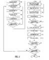
- FIG. 2illustrates a flow diagram of a method to form a layer by atomic layer deposition according to various embodiments.
- the resulting laminate layermay act as a single layer having a general formula of the form Ti 1-X-Y Zr X Hf Y O 2 , where the individual layers forming the final layer may be stoichiometric pure films, such as TiO 2 , or may be close to the stoichiometric ratio, or may be non-stoichiometric, as the final film may also have any ratio of component parts.
- the individual layersmay be crystalline or amorphous, depending upon the deposition parameters and any subsequent heat processing, such as may be found in typical MOS device processing.
- the individual layersmay be dielectric, conductive or semiconductive in nature.
- a substratemay be prepared to react immediately with, and chemisorb the first precursor gas.
- This preparationmay serve to remove contaminants such as thin organic films, dirt, and native oxide from the surface of the substrate, and it may include a hydrofluoric acid rinse, a hydrogen termination process to provide a activated surface, or a sputter etch.
- a first precursor materialmay enter the reaction chamber for a predetermined length of time, in an embodiment Hf(NO 3 ) 4 , for example from 0.5-2.0 seconds, but other hafnium-containing gases, liquids and sublimating solids may also be used as discussed previously.
- Hf(NO 3 ) 4is that the final film may be free of carbon, hydrogen or halogen contamination.
- the first precursor materialmay be chemically adsorbed onto the surface of the substrate, the amount depending at least in part upon the temperature of the substrate, which in one embodiment is 300° C., and at least in part on the presence of sufficient flow of precursor material.
- the initial filmdoes not have to be hafnium oxide, and it may equally well be titanium or zirconium.
- a first purge gasmay enter the reaction chamber for a predetermined length of time sufficient to remove substantially all of the non-chemisorbed first precursor material. Typical times may be 0.4-2.0 seconds, with the purge gas comprising nitrogen, argon, neon, hydrogen and combinations thereof.
- a first reactant gasmay enter the chamber for a predetermined length of time sufficient to provide enough of the reactant material to chemically combine with substantially all of the chemisorbed first precursor material on the surface of the substrate.
- the reactant material for the first precursorcomprises water vapor (i.e., H 2 O) for a pulse length of about 0.60 seconds.
- Suitable reactant materialsmay include mildly oxidizing materials, including, but not limited to, water vapor, hydrogen peroxide, nitrogen oxides such as nitrous oxide, ozone, oxygen gas, plasmas of the same, and combinations thereof.
- a second purge gaswhich may be the same or different from the first purge gas, may enter the chamber for a predetermined length of time, sufficient to remove substantially all non-reacted materials and reaction byproducts from the chamber. At this point, it may be said that a single ALD cycle has been completed.
- a decisionmay be made as to whether the thickness of the first material in the illustrative laminate layer has reached the desired thickness, or whether another deposition cycle should be performed.
- the thickness of the HfO 2 layer obtained from a single ALD cyclemay be 0.33 nm. If another deposition cycle is used to reach the desired thickness, then the operation may return to block 204 and repeat the deposition process until the desired first dielectric layer is completed. If the thickness of the first dielectric material is at or above the desired thickness, the process may move to the deposition of the second material at block 214 .
- a second precursor material for the second materialmay enter the reaction chamber for a predetermined length of time, typically 0.5-2.0 seconds.
- the precursor materialmay include tetrakisdiethylamino zirconium, TDEAZ, but other zirconium-containing materials, in gas, liquid or sublimating solid form may also be used.
- the second precursor materialmay be chemically adsorbed onto the surface of the substrate, in this case being the top surface of the first material.
- the absorption levelmay depend upon the temperature of the substrate, in one embodiment 300° C., and the presence of sufficient flow of the precursor material.
- the pulsing of the precursormay use a pulsing period that provides uniform coverage of an absorbed monolayer on the substrate surface, or it may use a pulsing period that provides partial formation of a monolayer on the substrate surface.
- the first purge gasis shown as entering the chamber, but the invention is not so limited.
- the purge gas used in the second dielectric material depositionmay be the same or different from either of the two previously noted purge gases, and FIG. 1 may be shown as having more than the one purge gas source shown.
- the purge cyclecontinues for a predetermined length of time sufficient to remove substantially all the non-chemisorbed second precursor.
- a second reactant gaswhich may the same or different from the first reactant gas, may enter the chamber for a predetermined length of time, sufficient to provide enough of the reactant to chemically combine with the chemisorbed second precursor material on the surface of the substrate.
- the reactant used with the TDEAZ precursorcomprises water vapor with a pulse time of about 2.0 seconds, resulting in a 0.10 nm layer of ZrO 2 .
- another purge gasenters the chamber, which may be the same or different from any of the three previously discussed purge gases, for a predetermined length of time, sufficient to remove non-reacted materials and any reaction byproducts from the chamber.
- a decisionmay be made as to whether the thickness of the second dielectric material in the laminate dielectric structure has reached a predetermined thickness, or whether another deposition cycle is desired. If another deposition cycle is needed, then the operation may return to 214 , until the second layer is completed.
- the thicknesses of the first and second materials in the laminatemay not be the same, and there may be more deposition cycles for one material than for the other.
- the processmay move to block 224 , where a third precursor enters the reactor.
- the third precursoris a titanium tetrachloride pulse lasting about 0.20 seconds at approximately 300° C. Again, the third precursor chemisorbs onto the surface, at this point the second film, ZrO 2 .
- the illustrative embodimenthas a particular order of precursors; however the invention is not so limited, and any of the three precursors may be used in any order, in accordance with the final film characteristics.
- another purgeoccurs to remove non-chemisorbed portions of the third precursor, and at block 228 the third reactant is pulsed into the reactor.
- the third reactantmay be the same as the previous reactants, or the third reactant may be a different material, and in an embodiment it is water vapor pulsed for about 0.20 seconds.
- another purgeoccurs.
- the desired thicknesses of the first, second and third materials in the laminate structuremay not be the same thickness, and there may be more deposition cycles for one material as compared to the others. If the third material has reached the desired thickness, the operation may move to block 234 , where it is determined if the first, second and third materials have reached the desired number of layers for the finished film. If more than a single layer of each material is desired, then the process may move back to another deposition of the first material at block 204 .
- the depositionmay end at block 236 .
- the present embodimentdiscusses and illustrates the layers as distinct from each other, the individual layers may be very thin and may act effectively as a single alloy layer, or subsequent heat cycles may anneal or alloy the individual layers into a single material layer.
- the present embodimentillustrates the hafnium oxide layer as being deposited first, but the invention is not so limited. The embodiment may not be limited to the described three material layers. Altering the deposition temperature and relative proportions of the precursors may result in a crystalline semiconductor layer of titanium zirconium hafnium oxide having ferromagnetic properties, rather than a dielectric.
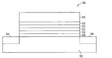
- FIG. 3illustrates a transistor 300 containing a structure deposited according to various embodiments.
- the first layermay contain a titanium oxide alternating with a hafnium oxide layer and with a zirconium oxide layer forming a deposited zirconium oxide/hafnium oxide/titanium oxide gate insulator layer.
- a substrate 302may be prepared for deposition, typically a silicon or silicon-containing material; however, other semiconductor materials such as germanium, gallium arsenide, and silicon-on-sapphire may also be used. This preparation process may include cleaning substrate 302 and forming various layers and regions of the substrate, such as drain diffusion 304 and source diffusion 306 of an illustrative metal oxide semiconductor (MOS) transistor 300 , prior to forming a gate dielectric.
- MOSmetal oxide semiconductor
- the substrate 302is typically cleaned to provide an initial substrate depleted of its native oxide, since the presence of a thin layer of SiO 2 may result in decreased capacitive coupling.
- the substratemay also be cleaned to provide a hydrogen-terminated surface, which may be known as an activated surface, to improve the rate of chemisorption.
- a silicon substratemay undergo a final hydrofluoric (HF) acid rinse prior to ALD processing to provide the silicon substrate with a hydrogen-terminated surface having no native silicon oxide layer. Cleaning preceding atomic layer deposition may aid in reducing the presence of silicon oxide at an interface between the silicon-based substrate and the dielectric formed using the atomic layer deposition process.
- the sequencing of the formation of the regions of the transistor being processedmay follow typical sequencing that is generally performed in the fabrication of a MOS transistor, as is well known to those of ordinary skill in the art.
- the dielectric covering the area on the substrate 302 between the source and drain diffused regions 304 and 306is deposited by ALD in this illustrative embodiment, and it comprises titanium oxide layers 308 and 314 , having interleaved zirconium oxide layers, 310 and 316 , and a single hafnium oxide layer 312 in the middle.
- the single shown layer 312 of hafnium oxideis not intended to be limiting, and the number of different layers may depend upon the desired final composition, which may affect the oxygen barrier properties and dielectric constant.
- This alloy dielectric structuremay be referred to as the gate oxide.
- the titanium oxide layer 308is shown as being the first layer and in direct contact with the substrate 302 ; however, the invention is not so limited.
- the embodimentmay also include having the first dielectric layer be zirconium oxide, since this may affect the level of surface states and the work function of the dielectric layer.
- the embodimentalso shows the different dielectric layers having the same thickness; however the desired properties of the film, such as dielectric constant, may be best achieved by adjusting the ratio of the thickness of the dielectric materials to different values.
- the gate oxide(all the layers 308 to 316 ) in total may appear to be a single alloyed dielectric layer having a formula of Ti 1-X-Y Zr X Hf Y O 2 .
- the transistor 300has a conductive material forming a single gate electrode 318 in this embodiment, but the dielectric may also be used in a floating gate device such as flash memory.
- gate dielectric(comprising layers 308 , 310 , 312 , 314 , 316 ) may form a tunnel gate insulator and a floating gate dielectric in a flash memory device.
- dielectric layers containing laminated ALD dielectric layers for a gate dielectric and/or floating gate dielectric in which the dielectric layer contacts a conductive layeris not limited to silicon-based substrates, but it may be used with other semiconductor substrates.
- FIG. 4illustrates a capacitor 400 containing a dielectric structure deposited according to various disclosed embodiments.
- Embodiments of methods for forming ALD deposited structures contacting a conductive layermay also be applied to forming spintronic devices such as tunnel devices and non-volatile memory devices, as well as capacitors in various integrated circuits, memory devices, and electronic systems.
- a methodmay include forming a first conductive layer 402 , a second conductive layer 404 , and a dielectric having interleaved layers 406 , 408 , 410 , 412 , 414 and 416 of at least three different dielectric materials, formed between the two conductive layers.
- the conductive layers 402 , 404may comprise metals, doped polysilicon, silicided metals, polycides, or conductive organic compounds, without affecting the teaching of this embodiment.
- the sequencing of the layersmay depend upon the application, or it may be less important in the case of an alloyed single layer, such as the described embodiment of an effectively single dielectric structure having layers 406 and 412 formed of HfO 2 , layers 408 and 414 formed of ZrO 2 , and layers 410 and 416 formed of titanium oxide, but the invention does not require that there be an even number of layers, or that the layers be deposited in any particular order, or that the order be repeated.
- the effective dielectric constant associated with a laminate structuremay be attributable to N capacitors in series, where each capacitor has a thickness defined by the thickness of the corresponding layer.
- a laminated structurecan be engineered to have a predetermined dielectric constant.
- Structures such as laminate structure shown in FIGS. 3 and 4may be used in non-volatile flash memory devices as well as other integrated circuits.
- Transistorse.g., a bipolar transistor, a MOS transistor
- capacitors, and other devices having dielectric filmsmay be implemented into memory devices, logic devices, mixed signal devices, displays, set top boxes and electronic systems including information-handling devices. Embodiments of these information-handling devices may include wireless systems, telecommunication systems, computers, portions of vehicles and integrated circuits.
- FIG. 5is a simplified diagram of a controller coupled to an electronic device according to various embodiments.
- An embodimentincludes an illustrative electronic system 500 having one or more devices including a dielectric structure containing an atomic layer deposited oxide layer formed according to various embodiments of the present invention.
- the electronic system 500may include a controller 502 , a bus 504 , and an electronic device 506 , where bus 504 provides electrical conductivity between controller 502 and electronic device 506 .
- the controller 502 and/or electronic device 506may include a dielectric structure containing an ALD deposited oxide layer as previously discussed herein.
- System 500may include information-handling, wireless, telecommunication, fiber optic, automotive, electro-optic, and computer systems.
- FIG. 6illustrates a diagram of an electronic system 600 having at least some devices with a dielectric film formed according to various disclosed embodiments.
- An embodiment of an electronic system 600may include a controller 602 and a memory 606 .
- Controller 602 and/or memory 606may include a dielectric layer having an ALD dielectric layer.
- the system 600also may include an electronic apparatus 608 , and a bus 604 , where the bus 604 may provide electrical conductivity and data transmission between controller 602 and electronic apparatus 608 , and between controller 602 and memory 606 .
- the bus 604may include an address, a data bus, and a control bus, each independently configured.
- the bus 604may use common conductive lines for providing address, data, and/or control, the use of which may be regulated by the controller 602 .
- the electronic apparatus 608may include additional memory devices configured similarly to the memory 606 . Some embodiments may include one or more additional peripheral devices 610 coupled to the bus 604 .
- the controller 602comprises a processor. Any of the controller 602 , the memory 606 , the bus 604 , the electronic apparatus 608 , and peripheral devices 610 may include a dielectric structure having an ALD deposited oxide layer in accordance with the disclosed embodiments.
- System 600may include, but is not limited to, information-handling devices, telecommunication systems, personal communication systems, personal computing systems such as laptop computers and personal digital assistants (PDAs) and computers.
- Peripheral devices 610may include displays, additional storage memory, or other control devices that may operate in conjunction with controller 602 and/or memory 606 . It will be understood that embodiments are equally applicable to any size and type of memory circuit and are not intended to be limited to a particular type of memory device.
- Memory typesinclude a DRAM (Dynamic Random Access Memory), SRAM (Static Random Access Memory) or Flash memories.
- the DRAMmay comprise a synchronous DRAM commonly referred to as SGRAM (Synchronous Graphics Random Access Memory), SDRAM (Synchronous Dynamic Random Access Memory), SDRAM II, and DDR SDRAM (Double Data Rate SDRAM), as well as Synchlink or Rambus DRAMs and other emerging DRAM technologies.
- SGRAMSynchronous Graphics Random Access Memory
- SDRAMSynchronous Dynamic Random Access Memory
- SDRAM IISynchronous Dynamic Random Access Memory
- DDR SDRAMDouble Data Rate SDRAM
- wafer and substrateas used in this description may include any structure having an exposed surface with which to form an integrated circuit (IC) structure.
- substrateis understood to include semiconductor wafers.
- substrateis also used to refer to semiconductor structures during processing, and it may include other layers that have been fabricated thereupon. Both “wafer” and “substrate” may include doped and undoped semiconductors, epitaxial semiconductor layers supported by a base semiconductor or insulator, as well as other semiconductor structures well known to one skilled in the art.
- conductoris understood to generally include n-type and p-type semiconductors, and the term “insulator” or “dielectric” is defined to include any material that is less electrically conductive than the materials referred to as conductors or as semiconductors.
- horizontalas used in this application is defined as a plane parallel to the conventional plane or surface of a wafer or substrate, regardless of the orientation of the wafer or substrate.
- verticalrefers to a direction perpendicular to the horizontal as defined above. Prepositions, such as “on”, “side” (as in “sidewall”), “higher”, “lower”, “over” and “under” are defined with respect to the conventional plane or surface being on the top surface of the wafer or substrate, regardless of the orientation of the wafer or substrate.
- An embodiment of a method for forming an electronic or a spintronic devicemay include forming a metal oxide layer by an atomic layer deposition (ALD) to form a laminated or layered structure having layers of zirconium oxide (ZrO 2 ), hafnium oxide (HfO 2 ) and titanium oxide (TiO 2 ).
- the structuremay act as a single dielectric layer or a single magnetic layer, and it may be formed by depositing the various metal oxides by atomic layer deposition onto a substrate surface using precursor chemicals containing zirconium, followed by a purge and deposition of an oxidizing material such as ozone, hydrogen peroxide or water vapor to form a thin (often a single molecular layer) film of ZrO 2 .
- Formationmay continue with ALD depositing hafnium oxide using precursor chemicals containing hafnium, followed by a purge and deposition of an oxidizing material such as ozone or water vapor to form a thin film of HfO 2 , followed by ALD deposition of a titanium oxide layer using precursor chemicals containing titanium, followed by a purge and deposition of an oxidizing material such as ozone or water vapor to form a thin film of TiO 2 .
- the above three film formationsmay be repeated as often as necessary to form a thin laminate dielectric structure of the desired thickness.
- the order of forming the three filmsis not limited to the discussed order, but it may be varied to obtain any desired combination, and the final film may be high temperature processed to anneal, or alloy, the three layers to act as a single uniform layer rather than as three separate films.
- a dielectric structure formed of zirconium oxide, hafnium oxide and titanium oxidemay be beneficially used in electronic devices because the high dielectric constant (high k) of the film may provide the functionality of a thinner silicon dioxide film with fewer reliability issues.
- a ferromagnetic layer formed in a similar fashion, but under different conditions, which may include forming the TiO 2 under conditions appropriate for crystalline formation,may provide a useful layer for spintronic devices.
- Another embodimentmay include forming the dielectric or ferromagnetic structure as a single film having a formula of Ti 1-X-Y Zr X Hf Y O 2 .
- the filmmay be formed by atomic layer deposition by using a mixed precursor.
- An example of a process to form a single filmmay include the mixing of selected volumes of HfCl 4 , TiCl 4 , and ZrCl 4 , the introduction of the mixture into a reactor at 250° C. for a time sufficient to allow the mixed precursors to chemisorb onto the surface, for example 5 seconds.
- An argon purge flowmay follow the precursor flow for about 5 seconds, followed by a reactant flow of water vapor for about 5 seconds.
- the ALD cyclemay be completed by another argon purge flow for about 5 seconds, resulting in a thin substantially uniform layer having an approximate formula of Ti 1-X-Y Zr X Hf Y O 2 .
- the values of X and Ymay depend upon the chemisorption of the individual precursors, the volume of the individual precursors and the temperature.
- the precursors usedmay not have similar chemical structures as used in the present illustrative example, and any combination of different chemical types may be used.
- zirconium oxideto produce a controlled compositional spread of hafnium and titanium oxides may provide a more stable silicon insulator interface, may have a larger bandgap and thus better insulation properties, and may provide the ability to adjust the dielectric constant k, and the film microstructure to the particular electronic device application.
- the titanium oxidemay be grown in a crystalline form, either in a substantially pure form, or with a doping of hafnium and/or zirconium.
- the crystalline form of the Ti 1-X-Y Zr X Hf Y O 2 materialmay be used as a ferromagnetic material in spintronic devices.
- Embodimentsmay include structures for capacitors, transistors, memory devices, and electronic systems with dielectric structures containing an atomic layer deposited zirconium oxide, hafnium oxide and titanium oxide layers, having various individual layer thickness, layer order and number of layers of each individual material, and methods for forming such structures.
- Other embodimentsmay include the use of the crystalline form and include optoelectronic devices, spintronic devices and tunnel diodes.
- An embodiment of a methodmay include forming a dielectric structure including at least zirconium oxide, hafnium oxide and titanium oxide on a surface of a substrate, and forming a conductive layer on the dielectric layer.
- the conductive layermay be a gate electrode in a MOS transistor, a ferromagnetic layer in a spintronic device, or a driving electrode in a micromechanical device.
- the zirconium oxidemay have a formula ZrO 2
- the hafnium oxidemay have a formula of HfO 2
- the titanium oxidemay have a formula of TiO 2 .
- the zirconium, titanium and hafnium oxidesmay be amorphous, for example in a gate oxide, or may be crystalline, as in a spintronic layer.
- the zirconium oxide, hafnium oxide and titanium oxidemay be formed as a single layer formed in a single reaction, as well as in individual layers, and may have a formula of Ti 1-X-Y Zr X Hf Y O 2 .
- the values of X and Ymay be selected to obtain a film having a dielectric constant of greater than 20 for high k gate dielectric devices, or they may be selected to obtain a film having an optical band gap value of about 3.2, for spintronic devices.
- the values of X and Ymay be selected to obtain a ferro-magnetic film having a Curie temperature value of greater than 130° C., if the single layer has a crystal structure that may be either anatase titanium oxide, or rutile titanium oxide, both of which may be used as spintronic device layers.
- the filmwhether formed as a single layer, or as a series of layers that are annealed to form a single layer, may have X in a range of from 0.05 to 0.35, and Y in a range of from 0.05 to 0.25, and still maintain its crystalline nature and spintronic effect.
- a particular set of values, where X may be 0.10, and Y may be 0.18,may result in a spintronic layer having a high optical bandgap of about 3.26, which may be useful in spintronic and optoelectronic devices.
- the Ti 1-X-Y Zr X Hf Y O 2 layermay be produced in various ways, but the uniformity of the layer thickness and the smoothness of the surfaces may be important in both spintronic applications, where the tunneling may be sensitive to layer thickness, and in electronic applications, where the leakage current through a gate dielectric may be sensitive to thickness and asperities.
- a deposition method that may address these possible issuesmay include forming the zirconium oxide, hafnium oxide and titanium oxide by atomic layer deposition.
- Hafnium oxide/zirconium/titanium oxide layers formed by ALDmay be processed at relatively low temperatures, such as 300° C., and may be amorphous and possess smooth surfaces. Such oxide films may provide enhanced electrical properties as compared to those formed by physical deposition methods, such as sputtering, or typical chemical layer depositions, due to their smoother surface and reduced damage, which may result in reduced leakage current. The use of such oxide films or layers may increase the dielectric constant and electrical insulation properties of the final film.
- Such dielectric layersmay have adjustable dielectric constants that are higher than the commonly used silicon dioxide and silicon nitride based dielectrics, and they may provide a significantly thicker physical thickness than a silicon oxide layer having the same equivalent oxide thickness, where the increased thickness may reduce leakage current and reduce oxide shorts due to pinholes and other reduced thickness areas. These properties may allow application as dielectric layers in numerous electronic devices and systems.
- Capacitors, transistors, higher level ICs or devices including memory devices, and electronic systemsmay be constructed utilizing the described ALD process for forming a dielectric film having a thin equivalent oxide thickness, t eq .
- Gate dielectric layers or films containing atomic layer deposited metal oxideshave a dielectric constant (k) substantially higher than that of silicon dioxide, such that these dielectric films are capable of a t eq thinner than SiO 2 gate dielectrics of the same physical thickness.
- the high dielectric constant relative to silicon dioxidemay enable the use of a greater physical thickness of these high k dielectric materials for the same t eq of SiO 2 .
- These described dielectric structuresmay be portions of various other devices, such as cameras, phones, wireless communication devices, displays, chip sets, set top boxes, games or vehicles.
- Spintronic devices and optoelectronic devicesmay use the described crystalline films in diluted magnetic semiconductor (DMS) devices and transparent ferromagnetic devices, such as magneto-optical devices with Currie temperatures well above room temperature, as high as 400° K., or 130° C.
- Spintronic devicesmay include tunnel diodes and non-volatile memory devices.
- the filmmay be a crystalline wide bandgap semiconductor oxide, and it may have the specific crystal structure known as rutile, or the crystal structure known as anatase. It will be understood by one of ordinary skill in the art that specific amounts described herein, such as times, pressures, dimensions, quantities, and the like are approximate and may be suitably adjusted.
Landscapes
- Chemical & Material Sciences (AREA)
- Engineering & Computer Science (AREA)
- Mechanical Engineering (AREA)
- General Chemical & Material Sciences (AREA)
- Organic Chemistry (AREA)
- Metallurgy (AREA)
- Materials Engineering (AREA)
- Chemical Kinetics & Catalysis (AREA)
- Microelectronics & Electronic Packaging (AREA)
- Condensed Matter Physics & Semiconductors (AREA)
- Power Engineering (AREA)
- General Physics & Mathematics (AREA)
- Physics & Mathematics (AREA)
- Computer Hardware Design (AREA)
- Manufacturing & Machinery (AREA)
- Inorganic Chemistry (AREA)
- Insulated Gate Type Field-Effect Transistor (AREA)
- Formation Of Insulating Films (AREA)
Abstract
Description
- This application, in a number of embodiments, relates generally to semiconductor devices and device fabrication, including dielectric structures and their method of fabrication.
- A market-driven need exists to continue to reduce the size of electronic devices containing semiconductor devices in order to obtain lower power consumption, lower operating voltages and higher performance. Smaller electronic devices typically reduce transistor size to obtain improved performance, which may entail reducing the thickness of the gate dielectric (typically silicon dioxide, SiO2) in proportion to the shrinkage of the gate length. For example, a metal-oxide-semiconductor field effect transistor (MOSFET) might have a 1.5 nm thick SiO2gate dielectric for a gate length of 70 nm. Smaller, more reliable integrated circuits (ICs) may be used in products such as processor chips, mobile telephones, games, displays and memory devices, such as dynamic random access memories (DRAMs).
- Another method of improving IC devices may include the use of what may be known as “ferroelectric devices” for non-volatile memory devices, and the use of ferro-magnetic semiconductors in forming what may be known as “spintronic devices”. Conventional electronic devices may rely upon the transport of electrons over conductors to form signals. Spintronic devices may exploit the spin of the electrons to form smaller, more robust and more versatile devices that may be more resistant to outside interference than other electronic devices. Electrons may have a property known as “spin”, which refers to the direction of the spin axis of the particle, which may be either spin-up or spin-down. When the electron spins within a group of electrons in a conductor are all aligned (i.e., either essentially all spin-up or all spin-down), they may create a large scale net magnetic moment. The aligned electron spins may create an analog to the situation found in a conventional magnetic material, such as the ferromagnetic elements iron and cobalt, wherein an application of a strong external magnet field can cause all of the spins of the iron or cobalt atoms to align and form a permanent magnet.
- Since about 1988, spintronic devices have been known following the discovery of the principle of giant magneto-resistance (GMR), which causes relatively large changes in electrical resistance in ultrathin magnetized layers under an applied external magnetic field. This discovery resulted in the design of magnetic memory devices with small magnetic regions that are sensitive to small magnetic fields, and magnetic disks that could hold up to twenty times the amount of data as previous magnetic disks. By flipping the impressed magnetization of the ultra-thin layers, spintronic devices may also be operated as switches that may be used to form random access memory (RAM) devices similar to semiconductor memories such as DRAMs, but with the advantage of being non-volatile. Such magnetic RAMs may be called “MRAMs”, which may be smaller, faster, and cheaper, use less power and be more resistant to high temperatures and high radiation levels than other memories.
- Spintronic devices may also be used as tunnel diodes having electrons that tunnel from a magnetic layer through an ultra thin insulating metal oxide layer to another magnetic layer. The electrons tunnel only when the magnetization alignments of the two magnetic layers are in the same direction. The amount of relative tunneling current may depend upon the width of what is known as the “bandgap” of the metal oxide layer, as well as upon the physical thickness of the metal oxide layer. Such layers may include cobalt doped rutile crystals.
- The semiconductor industry has relied upon reducing the dimensions of basic devices, for example the silicon based MOSFET, by a process that may be known as “scaling”. Device scaling may include scaling the gate dielectric, which has primarily been fabricated of silicon dioxide. A thermally grown amorphous SiO2layer may provide an electrically and thermodynamically stable material, where the interface of the SiO2layer with the underlying silicon may have a high quality charge state and good electrical isolation properties. However, increased scaling in microelectronic devices has demonstrated the potential benefits of using other dielectric materials as gate dielectrics, in particular dielectrics with higher dielectric constants to replace the use of various combinations of silicon dioxide SiO2, silicon nitride Si3N4and silicon oxynitride SiON. For higher dielectric constant materials (high “k”) to be practical, they may have the properties of high permittivity, thermal stability, high film and surface quality and smoothness, low hysteresis, low leakage current density, and long-term reliability. High k films may be metal oxide unary materials such as Al2O3, CeO2, TiO2, HfO2and ZrO2, which have a single component, or they may be binary systems such as (Y2O3)x(ZrO2)1-X, LaAlO3, and (HfO2)(Al2O3), which have two components, or they may be ternary systems having three components such as (HfO2) (ZrO2) (SnO2), and so on. High k films may be single layers, or they may be formed of multiple layers of different materials that act as a composite material. A high k dielectric may be amorphous to maintain surface smoothness and prevent electric field concentration at sharp projections (asperities), and to minimize leakage current along crystal boundaries.
FIG. 1 depicts an atomic layer deposition system for forming a layer of zirconium oxide, hafnium oxide, and titanium oxide layers, according to various embodiments;FIG. 2 illustrates a flow diagram of a method to form a layer by atomic layer deposition according to various embodiments;FIG. 3 illustrates a transistor containing a layer deposited according to various embodiments;FIG. 4 illustrates a capacitor containing a dielectric layer deposited according to various embodiments;FIG. 5 is a simplified diagram of a controller coupled to an electronic device, according to various embodiments; andFIG. 6 illustrates a diagram of an electronic system having at least some devices with a dielectric film formed according to various embodiments.- A gate dielectric in a transistor may have both a physical gate dielectric thickness and an equivalent oxide thickness (EOT or teq). The equivalent oxide thickness (EOT) quantifies the electrical properties, such as capacitance, of the high k gate dielectric in terms of a representative physical thickness of a silicon dioxide gate dielectric. The term teqmay be defined as the thickness of a theoretical SiO2layer that may have the same capacitance density as a given dielectric.
- A SiO2layer deposited on a Si surface as a gate dielectric may have a teqlarger than its physical thickness, t. This teqresults from the capacitance in the surface channel upon which the SiO2is deposited, due to the formation of a depletion/inversion region. The depletion/inversion region may result in teqbeing from 3 to 6 Angstroms (Å) larger than the physical SiO2thickness, t. With the semiconductor industry moving to scale the gate dielectric equivalent oxide thickness to less than 10 Å, the physical thickness for a SiO2layer used for a gate dielectric may be approximately 4 to 7 Å.
- Additional features for a SiO2gate dielectric layer may depend upon the properties of the gate electrode used in conjunction with the SiO2gate dielectric. Using a conventional polysilicon gate may result in an additional increase in teqfor the SiO2layer. The additional teqvalue may be reduced by using a metal gate electrode, although metal gates are not typically used in typical complementary metal-oxide-semiconductor (CMOS) field effect transistor technology. Thus, future devices may have a physical SiO2gate dielectric layer of about 5 Å or less. Such a thin SiO2oxide layer may create current leakage issues across the thin oxide.
- Silicon dioxide may be commonly used as a gate dielectric, in part, due to its electrical isolation properties in a SiO2—Si based structure. This electrical isolation may be due to the relatively large bandgap of SiO2(8.9 eV) resulting in a relatively good electrical insulator. Significant reductions in bandgap value below SiO2reduce the utility of a material for use as a gate dielectric. However, as the thickness of a SiO2layer decreases, the number of atomic layers, or monolayers of the material in the layer typically decreases. At some thickness, the number of monolayers may be so small that the SiO2layer may not have as complete an arrangement of atoms as found in a thicker, or bulk, layer. As a result of incomplete formation relative to a bulk structure, a thin SiO2layer of only one or two monolayers may fail to form a full band gap. The lack of a full bandgap in a SiO2gate dielectric may cause an effective short between an underlying conductive silicon channel and an overlying conductive gate. This undesirable property tends to limit the minimum physical thickness to which a SiO2layer may be scaled, and it is thought to be about 7-8 Å. Therefore, for future devices to have a teqless than about 10 Å, dielectrics other than SiO2may be considered for use as a gate dielectric.
- For a dielectric layer used as a gate dielectric, the capacitance may be determined as in a parallel plate capacitance: C=kε0A/t, where k is the dielectric constant, ε0is the permittivity of free space, A is the area of the capacitor, and t is the thickness of the dielectric. The thickness, t, of a material may be related to its teqfor a given capacitance, with SiO2having a dielectric constant kox=3.9, as
t=(k/kox)teq=(k/3.9)teq.- Thus, materials with a dielectric constant greater than that of SiO2(typically about 3.9) may have a physical thickness considerably larger than a desired teq, while providing the desired equivalent oxide thickness. For example, an illustrative dielectric material with a dielectric constant of 10, such as aluminum oxide Al2O3, may have a thickness of 25.6 Å to provide a teqof 10 Å. Thus, a reduced equivalent oxide thickness for transistors may be realized by using dielectric materials with higher dielectric constants than SiO2.
- As noted above, an equivalent oxide thickness for lower transistor operating voltages and smaller transistor dimensions may be realized by using materials having a higher dielectric constant. However, additional fabricating issues may make determining a suitable replacement for SiO2difficult. If the use of silicon-based devices continues, then potentially significant constraints on the substitute dielectric material may occur. During the formation of the dielectric on the silicon layer, there exists the possibility that a small layer of SiO2may be formed in addition to the desired dielectric. The electrical result may comprise a dielectric layer having two sub-layers connected to each other and to the silicon layer on which the dielectric is formed. In such a case, the resulting capacitance would be that of two dielectrics in series. Thus, the teqof the dielectric layer may be considered as the sum of the SiO2thickness and a multiplicative factor of the thickness t of the dielectric being formed, written as
teq=tSiO2+(kox/k)t.- If a SiO2layer is formed in the process of forming the high k dielectric, the teqmay again be limited by the SiO2layer. Thus, a useful property of a high k dielectric may be an oxygen barrier to prevent a layer of SiO2from forming on the silicon surface. The layer directly in contact with the silicon layer may provide a high quality interface for high channel carrier mobility and low surface charge density.
- One of the advantages of using SiO2as a gate dielectric may be that the formation of the SiO2layer may result in an amorphous gate dielectric. An amorphous structure for a gate dielectric may provide reduced leakage current problems associated with grain boundaries in polycrystalline gate dielectrics, sometimes implicated in high current leakage paths. Crystal grain size and orientation changes throughout a polycrystalline gate dielectric may cause variations in the film's dielectric constant, along with uniformity and surface topography issues. Materials having a high dielectric constant relative to SiO2may also have the disadvantages of a crystalline form, and they may have a lower bandgap width.
- Another consideration for selecting the material and method for forming a dielectric film for use in electronic and spintronic devices may be the roughness of the dielectric film on a substrate. Surface roughness may have a significant effect on the electrical properties of the gate oxide and on the resulting operating characteristics of the transistor. The leakage current through a physical 1.0 nm gate dielectric may increase by a factor of 10 for every 0.1 increase in the root-mean-square (RMS) roughness of the dielectric layer. Such surface damage may occur during a conventional sputtering deposition process, when particles of the material to be deposited may bombard the surface at a high energy. When a sputtered particle hits the surface, some particles may adhere, and other particles may cause surface damage by knocking out a portion of the surface layer creating pits. The surface of such a deposited dielectric layer may have a rough contour due to the rough interface at the body region, and thus the electrical properties of a thin film may not be as good as the values in a bulk sample of the same material. Thus the method used to form the thin film dielectric may have a substantial impact on the usefulness of the material in electronic devices. Atomic layer deposition (ALD) may provide a dielectric layer with superior surface uniformity and thickness control than other deposition methods. The use of ALD may result in a dielectric layer grown on silicon having surface smoothness of about 0.20 nm root mean square (RMS) value on a 20 nm thick layer, which may result in less electric field concentration at insulator corners and projections, and lower leakage currents.
- Titanium oxide has a dielectric constant of 30-35, an electronic bandgap of about 5.0 eV and an optical bandgap of about 3.10 in a crystal form. Zirconium oxide has a dielectric constant of 18-23, a bandgap of about 6.0 eV, and an optical bandgap of about 3.16 eV in a 50% combination with titanium oxide crystals. Hafnium oxide has a dielectric constant of 17-22, a bandgap of about 5.6 eV, and an optical bandgap of about 3.28 eV in a 50% combination with titanium oxide crystals. Mixing hafnium and zirconium in doped titanium oxide may allow an optical bandgap as high as 3.30 eV, although the crystalline nature of the titanium oxide may suffer at doping levels of zirconium above 35%, or of hafnium above 25%. A maximum realistic optical bandgap of about 3.26 eV may be found at a zirconium doping level of 10% and a hafnium doping level of 18%, which may then have a total zirconium level of 72% in the crystal. It may be useful to provide spintronic devices having crystalline films with an adjustable optical band gap that may be controllably varied from 3.15 to 3.26 eV.
- In high k dielectrics for transistor gate dielectrics, which as noted above may be beneficially amorphous, hafnium oxide may have a conduction band/valence band offset versus that of silicon of 2.0 eV/2.5 eV, which may be useful in reducing leakage currents. However, hafnium oxide may lose its amorphous nature at temperatures of about 500° C., which is a temperature below that found in typical MOS processes that may follow the gate dielectric deposition. Another issue with layers containing hafnium oxide is that oxygen may diffuse through the hafnium oxide during subsequent furnace operations, which may form a SiO2layer underneath the hafnium oxide at the silicon interface. This may result in reduced capacitive coupling between the gate electrode and the semiconductor. Zirconium oxide containing layers may have improved thermal stability as compared to hafnium oxide alone, and zirconium oxide containing layers may have superior silicon interface properties since the atomic size of zirconium may match hafnium atoms better than titanium. The resulting three part structure of titanium, hafnium, and zirconium oxides may remain amorphous through the thermal cycles of typical semiconductor processing up to 900 to 1,000° C., due to the zirconium content, and the dielectric constant may still be higher than 25 due to the high k of the titanium oxide portion of the layer. Current leakage across the dielectric may range between 10−7A/cm2to 10×10−9A/cm2, depending upon the composition, and it may form useful dielectric layers for semiconductor device gate insulators. The optical band gap may be varied from the low of titanium oxide crystals, to the high of zirconium oxide doped crystals by varying the composition, and thus the ternary oxide may be useful in spintronic devices. ALD deposition may have composition control superior to other deposition methods and may more uniformly select and control the material band gap, which may be useful in spintronic devices, for example by doping titanium oxide layers with hafnium and zirconium to obtain a ferromagnetic crystalline material.
- Forming such films using atomic layer deposition can enable controlling transitions between different material layers. As a result of such control, ALD deposited dielectric films may have an engineered transition with a substrate surface, or they may be formed of many thin layers of different dielectric materials to enable selection of the dielectric constant to a value that is between the values obtainable from pure dielectric compounds.
- ALD is a modification of chemical vapor deposition (CVD) and may also be called “alternatively pulsed-CVD”. In ALD, chemical precursors may be introduced one at a time to the substrate surface mounted within a reaction chamber (or reactor). This introduction of chemical precursors may take the form of pulses of each precursor. The precursor is made to flow into a specific area or region for a short period of time. Between the pulses, the reaction chamber may be purged with a gas, which may be an inert gas, and/or the chamber may be evacuated. ALD may occur at atmospheric pressure or in relatively high vacuum levels.
- In the first reaction of the ALD process, the first precursor may saturate and may be chemisorbed (or adsorbed) onto the substrate surface during the first pulsing phase. Subsequent pulsing with a purging gas may remove non-chemisorbed precursor from the reaction chamber.
- A second pulsing phase may introduce a second precursor (which may be referred to as a “reactant”) to the substrate where the growth reaction of the desired film may take place, with a reaction thickness that may depend upon the amount of chemisorbed first precursor. Subsequent to the film growth reaction, reaction byproducts and precursor excess may be purged or evacuated from the reaction chamber. A precursor chemistry, having precursors that adsorb and aggressively react with each other on the substrate, may enable one ALD cycle to be performed in less than one second in a flow type reaction chamber. Precursor pulse times may range from about 0.3 sec to 3 seconds.
- In ALD processes, the saturation of all the reaction and purging phases may make the film growth self-limiting. Self-limiting growth may result in large area uniformity and conformality, having applications in such cases as planar substrates, filling deep trenches, and in the processing of porous silicon and high surface area silica and alumina powders. ALD may operate to control film thickness in a straightforward manner by controlling the number of growth cycles.
- Precursors used in an ALD process may be gaseous, liquid or solid, however, liquid or solid precursors may be volatile with a vapor pressure high enough for effective mass transportation. Solid precursors and liquid precursors may work better when heated and introduced through heated tubes to the substrates. An adequate vapor pressure may be reached at a temperature that is below the substrate temperature to minimize condensation of the precursors on the substrate. The self-limiting growth mechanisms of ALD may allow relatively low vapor pressure solid precursors to be used, though evaporation rates may vary during processing because of changes in solid surface area.
- The precursors used in ALD may be thermally stable at the substrate temperature since precursor decomposition may destroy surface control and the advantages of the ALD method, which may rely upon the reaction of the precursor at the substrate surface. A slight decomposition, if slow compared to the ALD growth rate, may be tolerated. The precursors may chemisorb on, or react with, the surface. The molecules at the substrate surface may react aggressively with the second precursor, which may be called a reactant, to form the solid film. Precursors should not react substantially with the formed film to cause etching, and precursors should not dissolve substantially in the film. The ability to use highly reactive precursors in ALD may contrast with the selection of precursors for conventional CVD type reactions. The by-products in the reaction may be gaseous in order to allow their removal from the reaction chamber during a purge stage. Further, it may be useful if the by-products do not react or adsorb on the surface.
- In an ALD process, the self-limiting process sequence may involve sequential surface chemical reactions. ALD may rely upon chemistry between a reactive surface and one or more reactive molecular precursors, which may be pulsed into the ALD reaction chamber separately. The metal precursor reaction at the substrate may be followed by an inert gas pulse (or purge) to remove a precursor and by-products from the reaction chamber prior to an input pulse of the next precursor of the fabrication sequence. By the use of ALD processes, films may be layered in substantially equal metered sequences that may be substantially the same with respect to chemical kinetics, deposition per cycle, composition, and thickness. ALD sequences generally deposit less than a full layer per cycle. Typically, a deposition or growth rate of about 0.25 to about 2.00 Å per cycle may be realized.
- Advantages of ALD depositions over other depositions such as CVD may include superior continuity at an interface avoiding poorly defined nucleating regions typically found in thin chemical vapor deposition (<20 Å) and physical vapor deposition (<50 Å) processes, superior conformality over a variety of substrate topologies due to its layer-by-layer deposition technique, use of low temperature and mildly oxidizing processes, lack of dependence on the reaction chamber, growth thickness that may depend solely on the number of cycles performed, and ability to engineer multilayer laminate films with resolution of one to two monolayers. ALD processes may permit deposition control on the order of single monolayers and the ability to deposit amorphous films.
- A cycle of an ALD deposition sequence may include a first precursor material pulse, a purging gas pulse, a second reactant precursor pulse, and the reactant's purging gas pulse, resulting in a deposition thickness that may be a function of the amount of the first precursor that absorbs onto, and saturates, the surface. This ALD cycle may be repeated until the desired thickness is achieved in a single material dielectric layer, or it may be alternated with pulsing a third precursor material, pulsing a purging gas for the third precursor, pulsing a fourth reactant precursor, and pulsing the reactant's purging gas. The resulting thin layers of different dielectric materials, which may be only a few molecular layers thick, may be known as a laminated film, or a “nanolaminate”. A nanolaminate may include a composite film of ultra-thin layers of two or more different materials in a layered stack, where the layers are alternating layers of different materials having a thickness on the order of a nanometer. The nanolayers may not be limited to alternating single layers of each material, but they may include several layers of one material alternating with a single layer of the other material, to obtain a ratio of the two or more materials. Such an arrangement may obtain a dielectric constant that is between the values of the two materials taken singly, or an adjustable band gap that is different from any of the individual layers. The final layer may be made of single layers of the two or more materials deposited individually, whether dielectric, conductive or semiconductive, but it may be considered a single film formed of an alloy between the individual films. This may depend upon the particular materials being used, their physical and chemical properties relative to one another, and any thermal cycling. Miscible materials may result in a single layer or alloy.
- In general, the composition of the deposition determines if the final material is conductive (a gate electrode in a MOS transistor), or ferromagnetic (a spintronic device, magnetic memory or a driving electrode in a micromechanical device), or a dielectric (an insulator in a transistor or capacitor). Depending upon the deposition parameters, the zirconium, titanium and hafnium oxides may be amorphous dielectrics having an engineered dielectric constant and used as a gate oxide in a high speed transistor. Under different conditions the result may be crystalline and used in a spintronic device. The zirconium oxide, hafnium oxide and titanium oxide may be formed as a single layer formed in a single reaction, and may have a formula of Ti1-X-YZrXHfYO2. Alternatively, they may be formed in separate layers in separate reactions, to obtain a desired semiconductor interface work function. The values of X and Y may be selected to obtain a film having a dielectric constant of greater than 20 for high k gate dielectric devices like transistors that operate faster and with lower power, or they may be selected to obtain a film having an optical band gap value of about 3.2, for spintronic devices. The values of X and Y may be selected to obtain a ferro-magnetic film having a Curie temperature value of greater than 130° C., and used in magnetic memory devices such as MRAMs. The Ti1-X-YZrXHfYO2layer may be produced in various ways, but the uniformity of the layer thickness and the smoothness of the surfaces may be important in spintronic applications, where the tunneling may be sensitive to layer thickness, and in electronic applications, where the leakage current through a gate dielectric may be sensitive to thickness, smoothness and asperities.
- In an embodiment, an ALD deposition of zirconium oxide, hafnium oxide and titanium oxide may be formed on a substrate mounted in a reaction chamber in a repetitive sequence using precursor gases individually pulsed into the reaction chamber. An embodiment may include forming a zirconium oxide layer using a metal alkoxy complex precursor gas, such as a tetrakis dialkyl amino zirconium, such as tetrakis dimethlyamine, having a chemical formula of Zr[N(CH3)2]4, or tetrakis ethylmethlyamine, having a chemical formula of Zr[N(CH3) (C2H5)], or tetrakis diethlyamine, having a chemical formula of Zr[N(C2H5)2]4, referred as TDEAZ, or other organometallic compounds. The TDEAZ may be pulsed for about 5 seconds at 350° C., followed by a purge of argon gas for about 5 seconds. Then oxygen may be pulsed for about 5 seconds followed by another argon purge of about 5 seconds, resulting in a zirconium oxide layer of about 0.5 nm per cycle and a surface smoothness of better than 0.5%. Similar results may be found using metal alkoxy complex precursors of hafnium and titanium, and other reactants.
- An embodiment may include forming the ZrO2layer using ALD with the organometallic compound zirconium tertiary-butoxide as the precursor, having a formula of Zr(OC4H9)4, and referred to as “ZTB”. The deposition may be preformed at 350° C. with water vapor as an oxidizing reactant. The ZTB may be pulsed for 10 seconds, followed by a purge of nitrogen gas for 10 seconds, and water vapor pulsed for 60 seconds, followed by another 10-second inert gas purge, resulting in a 0.05 nm layer of zirconium oxide. A precursor of zirconium tertiary-methoxide having a formula of Zr(O(CH3)3)4may be used at a temperature of approximately 250° C. with water vapor as a reactant. Other reactants may include ozone, oxygen, nitrous oxide and alcohol.
- Another embodiment may include forming a ZrO2layer using ALD with zirconium tetrachloride, having a formula of ZrCl4as the precursor. The deposition may be performed at 400 to 425° C. with water vapor as the oxidizing reactant. A 0.5 second pulse of ZrCl4may be followed by a 0.5 second purge with an inert gas, such as nitrogen, and a 0.5 second pulse of water vapor, resulting in a layer of zirconium oxide having a thickness of about 0.15 nm. Another embodiment includes deposition at 200° C. and may result in a thicker layer of zirconium oxide of 0.33 nm thickness. A similar embodiment may include using a precursor of zirconium tetraiodide having a formula of ZrI4at 300° C. with water vapor, resulting in about a 0.45 nm thickness per cycle.
- Another embodiment may include forming a ZrO2layer using ALD with a precursor comprising zirconium tetraisopropoxide, having a formula of Zr(O-i-Pr)4, which may be more thermally stable than other potential precursors. The deposition may be preformed at 425° C. with water vapor as the oxidizing reactant.
- Another embodiment may include forming a ZrO2layer using ALD with a precursor comprising zirconium nitrate, having a formula of Zr(NO3)4, which may be known as an anhydrous nitrate, with a reactant of water vapor at a temperature of from 160 to 180° C. The use of an anhydrous nitrate precursor may reduce the amount of carbon trapped in the film while depositing at a relatively low temperature.
- Various embodiments for forming hafnium oxide may include hafnium tetra chloride, hafnium tetra iodide, hafnium tetraisopropoxide, hafnium tertiary-butoxide, hafnium tertiary-methoxide, anhydrous hafnium nitrate or tetrakis dialkyl amino hafnium as the ALD precursor, and water vapor as the reactant material as discussed above for the zirconium depositions. Another embodiment may include hafnium nitride, Hf(NO3)4as the precursor at 300° C. with pulse times of 0.6 seconds, with a reactant of water vapor, resulting in about a 0.36 nm film per cycle. Hafnium oxide films may be formed at temperatures as low as 150° C. using a tetrakismethylethylamino hafnium precursor and may result in a slow controlled film growth of 0.09 nm per cycle.
- Various embodiments for forming titanium oxide may include titanium tetra chloride, titanium tetra iodide, titanium tetraisopropoxide, titanium tertiary-butoxide, titanium tertiary-methoxide, titanium nitrate or tetrakis dialkyl amino titanium as the ALD precursor, and water vapor as the reactant material, as discussed above for the zirconium and hafnium depositions. Titanium, zirconium and hafnium are chemically similar elements that occupy column IVA of the periodic table of elements.
- Other solid or liquid precursors may be used in an appropriately designed reaction chamber (known as a reactor) for any of the above materials. The use of such precursors in an ALD reaction chamber may result in lower deposition temperatures in the range of 180° C. to 400° C., and the ability to use mildly oxidizing reactant materials such as water (H2O), hydrogen peroxide (H2O2), various alcohol vapors, nitrous oxide (N2O) or other oxides of nitrogen, ozone (O3) or oxygen. Purge gases may include hydrogen, nitrogen, helium, argon, krypton or neon. It should be noted that the use of the term reactant may mean a precursor material that is added to the ALD reactor to react with the previously introduced precursor material, to form a layer of the product material. It should be noted that there may be no difference between a precursor material and a reactant material other than the order in which they enter the reactor. The terms are used to facilitate understanding the principles of the disclosed arrangements, and they are not intended to be used in a limiting sense.
- It should be noted that the above-mentioned embodiments are not intended to be limited to a single deposition cycle of each of the materials, but rather they may have multiple layers of one material deposited prior to the other materials being deposited, in order to obtain the desired final composition.
FIG. 1 depicts an atomiclayer deposition system 100 suitable for forming a layer of zirconium oxide, hafnium oxide, and titanium oxide. In an embodiment the layer may contain titanium oxide (either in a crystalline form such as rutile, or in an amorphous form) having an approximate formula of ZrO2, zirconium oxide having an approximate formula of ZrO2, and hafnium oxide having an approximate formula of HfO2, according to various embodiments. The elements depicted permit discussion of the described embodiments such that those skilled in the art may practice these embodiments without undue experimentation. InFIG. 1 , asubstrate 108 on a heating element/wafer holder 106 may be located inside areaction chamber 102 ofALD system 100. Theheating element 106 may be thermally coupled tosubstrate 108 to control the substrate temperature. A gas-distribution fixture 110 may introduce precursor, reactant and purge gases to the region of the surface ofsubstrate 108 in a substantially uniform fashion. The gases introduced by thegas distribution fixture 110, sometimes referred to as a showerhead, may react with thesubstrate 108, and excess precursor gases and reaction products may be removed from thechamber 102 by avacuum pump 104 through acontrol valve 105. Thesystem 100 may operate at any desired deposition pressure by controlling the volume of gas entering thechamber 102 as compared to the volume of gaseous reaction product and excess gases removed from thechamber 102 via control of the pumping rate ofvacuum pump 104 and thevalve 105. ALD systems may operate at normal atmospheric pressures, at above normal atmospheric pressure or may operate under vacuum conditions. In some embodiments, ALD layers may be formed at a reduced pressure of 10−5Torr pressure with an oxygen gas plasma with a 100 Watt radio-frequency (RF) generator (not shown) providing the oxidation reactant. Such an arrangement may result in a less contaminated final film, especially with respect to possible carbon contamination from excess carbon in some of the precursors discussed above, such as tetrakis diethlyamine, Zr[N(C2H5)2]4, or other organometallic compounds.- Each precursor, reactant or purge material may originate from
individual material sources flow controllers sources - Also included is a single
purging gas source 114, although the invention is not so limited, and numerous different purge gases, such as nitrogen, argon, helium, neon, hydrogen and krypton may be provided, and used either individually, in combination, simultaneously or sequentially. Thepurge gas source 114 is coupled to mass-flow controller 116. Two reactant material sources,130 and134, are connected through mass-flow controllers conduit 112, which may be coupled to the gas-distribution fixture 110 inside thereaction chamber 102.Gas conduit 112 may also be coupled to another vacuum pump, or exhaust pump, not shown, to remove excess precursor gases, purging gases, and by-product gases at the end of a purge cycle from thegas conduit 112. - The vacuum pump, or exhaust pump,104 may be coupled to
chamber 102 bycontrol valve 105, which may comprise a mass-flow valve, to remove excess precursor gases, purging gases, and by-product gases fromreaction chamber 102 at the end of a purging sequence. For convenience, control displays, mounting apparatus, temperature-sensing devices, substrate-maneuvering apparatus, and electrical connections, known to those skilled in the art are not shown inFIG. 1 . Though theALD system 100 shown inFIG. 1 is well suited for practicing the present illustrative embodiments, other commercially available ALD systems may also be used. - The use, construction and fundamental operation of reaction chambers for deposition of films are understood by those of ordinary skill in the art of semiconductor fabrication. The embodiments, as disclosed herein, as well as others, may be practiced on a variety of such reaction chambers without undue experimentation. One of ordinary skill in the art will comprehend the detection, measurement, and control techniques used in the art of semiconductor fabrication that are not specifically disclosed herein, and those skilled in the art will also appreciate that the individual elements such as pressure control, temperature control, and gas flow within
ALD system 100 can be under computer control, upon reading the disclosure. The elements ofALD system 100 may be controlled by a computer. FIG. 2 illustrates a flow diagram of a method to form a layer by atomic layer deposition according to various embodiments. Note that the resulting laminate layer may act as a single layer having a general formula of the form Ti1-X-YZrXHfYO2, where the individual layers forming the final layer may be stoichiometric pure films, such as TiO2, or may be close to the stoichiometric ratio, or may be non-stoichiometric, as the final film may also have any ratio of component parts. The individual layers may be crystalline or amorphous, depending upon the deposition parameters and any subsequent heat processing, such as may be found in typical MOS device processing. The individual layers may be dielectric, conductive or semiconductive in nature.- At
block 202, a substrate may be prepared to react immediately with, and chemisorb the first precursor gas. This preparation may serve to remove contaminants such as thin organic films, dirt, and native oxide from the surface of the substrate, and it may include a hydrofluoric acid rinse, a hydrogen termination process to provide a activated surface, or a sputter etch. - At block204 a first precursor material may enter the reaction chamber for a predetermined length of time, in an embodiment Hf(NO3)4, for example from 0.5-2.0 seconds, but other hafnium-containing gases, liquids and sublimating solids may also be used as discussed previously. One advantage of the use of Hf(NO3)4is that the final film may be free of carbon, hydrogen or halogen contamination. The first precursor material may be chemically adsorbed onto the surface of the substrate, the amount depending at least in part upon the temperature of the substrate, which in one embodiment is 300° C., and at least in part on the presence of sufficient flow of precursor material. The initial film does not have to be hafnium oxide, and it may equally well be titanium or zirconium.
- At block206 a first purge gas may enter the reaction chamber for a predetermined length of time sufficient to remove substantially all of the non-chemisorbed first precursor material. Typical times may be 0.4-2.0 seconds, with the purge gas comprising nitrogen, argon, neon, hydrogen and combinations thereof.
- At block208 a first reactant gas may enter the chamber for a predetermined length of time sufficient to provide enough of the reactant material to chemically combine with substantially all of the chemisorbed first precursor material on the surface of the substrate. In an embodiment, the reactant material for the first precursor comprises water vapor (i.e., H2O) for a pulse length of about 0.60 seconds. Suitable reactant materials may include mildly oxidizing materials, including, but not limited to, water vapor, hydrogen peroxide, nitrogen oxides such as nitrous oxide, ozone, oxygen gas, plasmas of the same, and combinations thereof.
- At block210 a second purge gas, which may be the same or different from the first purge gas, may enter the chamber for a predetermined length of time, sufficient to remove substantially all non-reacted materials and reaction byproducts from the chamber. At this point, it may be said that a single ALD cycle has been completed.
- At block212 a decision may be made as to whether the thickness of the first material in the illustrative laminate layer has reached the desired thickness, or whether another deposition cycle should be performed. In an embodiment, the thickness of the HfO2layer obtained from a single ALD cycle may be 0.33 nm. If another deposition cycle is used to reach the desired thickness, then the operation may return to block204 and repeat the deposition process until the desired first dielectric layer is completed. If the thickness of the first dielectric material is at or above the desired thickness, the process may move to the deposition of the second material at
block 214. - At block214 a second precursor material for the second material may enter the reaction chamber for a predetermined length of time, typically 0.5-2.0 seconds. In an embodiment the precursor material may include tetrakisdiethylamino zirconium, TDEAZ, but other zirconium-containing materials, in gas, liquid or sublimating solid form may also be used. The second precursor material may be chemically adsorbed onto the surface of the substrate, in this case being the top surface of the first material. The absorption level may depend upon the temperature of the substrate, in one
embodiment 300° C., and the presence of sufficient flow of the precursor material. In addition, the pulsing of the precursor may use a pulsing period that provides uniform coverage of an absorbed monolayer on the substrate surface, or it may use a pulsing period that provides partial formation of a monolayer on the substrate surface. - At
block 216 the first purge gas is shown as entering the chamber, but the invention is not so limited. The purge gas used in the second dielectric material deposition may be the same or different from either of the two previously noted purge gases, andFIG. 1 may be shown as having more than the one purge gas source shown. The purge cycle continues for a predetermined length of time sufficient to remove substantially all the non-chemisorbed second precursor. - At block218 a second reactant gas, which may the same or different from the first reactant gas, may enter the chamber for a predetermined length of time, sufficient to provide enough of the reactant to chemically combine with the chemisorbed second precursor material on the surface of the substrate. In an embodiment the reactant used with the TDEAZ precursor comprises water vapor with a pulse time of about 2.0 seconds, resulting in a 0.10 nm layer of ZrO2.
- At
block 220 another purge gas enters the chamber, which may be the same or different from any of the three previously discussed purge gases, for a predetermined length of time, sufficient to remove non-reacted materials and any reaction byproducts from the chamber. - At block222 a decision may be made as to whether the thickness of the second dielectric material in the laminate dielectric structure has reached a predetermined thickness, or whether another deposition cycle is desired. If another deposition cycle is needed, then the operation may return to214, until the second layer is completed. The thicknesses of the first and second materials in the laminate may not be the same, and there may be more deposition cycles for one material than for the other.
- If the second layer has reached the desired thickness, the process may move to block224, where a third precursor enters the reactor. In an embodiment the third precursor is a titanium tetrachloride pulse lasting about 0.20 seconds at approximately 300° C. Again, the third precursor chemisorbs onto the surface, at this point the second film, ZrO2. The illustrative embodiment has a particular order of precursors; however the invention is not so limited, and any of the three precursors may be used in any order, in accordance with the final film characteristics.
- At
block 226 another purge occurs to remove non-chemisorbed portions of the third precursor, and atblock 228 the third reactant is pulsed into the reactor. The third reactant may be the same as the previous reactants, or the third reactant may be a different material, and in an embodiment it is water vapor pulsed for about 0.20 seconds. Atblock 230 another purge occurs. - At block232 a decision is made as to whether or not the third material has reached the predetermined thickness. If another deposition cycle is needed, then the operation may return to block224, until the desired second dielectric layer is completed. The desired thicknesses of the first, second and third materials in the laminate structure may not be the same thickness, and there may be more deposition cycles for one material as compared to the others. If the third material has reached the desired thickness, the operation may move to block234, where it is determined if the first, second and third materials have reached the desired number of layers for the finished film. If more than a single layer of each material is desired, then the process may move back to another deposition of the first material at
block 204. After the number of interleaved layers of the first, second and third materials has reached the desired value, the deposition may end atblock 236. Although the present embodiment discusses and illustrates the layers as distinct from each other, the individual layers may be very thin and may act effectively as a single alloy layer, or subsequent heat cycles may anneal or alloy the individual layers into a single material layer. The present embodiment illustrates the hafnium oxide layer as being deposited first, but the invention is not so limited. The embodiment may not be limited to the described three material layers. Altering the deposition temperature and relative proportions of the precursors may result in a crystalline semiconductor layer of titanium zirconium hafnium oxide having ferromagnetic properties, rather than a dielectric. FIG. 3 illustrates atransistor 300 containing a structure deposited according to various embodiments. The first layer may contain a titanium oxide alternating with a hafnium oxide layer and with a zirconium oxide layer forming a deposited zirconium oxide/hafnium oxide/titanium oxide gate insulator layer. Asubstrate 302 may be prepared for deposition, typically a silicon or silicon-containing material; however, other semiconductor materials such as germanium, gallium arsenide, and silicon-on-sapphire may also be used. This preparation process may include cleaningsubstrate 302 and forming various layers and regions of the substrate, such asdrain diffusion 304 andsource diffusion 306 of an illustrative metal oxide semiconductor (MOS)transistor 300, prior to forming a gate dielectric. Thesubstrate 302 is typically cleaned to provide an initial substrate depleted of its native oxide, since the presence of a thin layer of SiO2may result in decreased capacitive coupling. The substrate may also be cleaned to provide a hydrogen-terminated surface, which may be known as an activated surface, to improve the rate of chemisorption. In an embodiment, a silicon substrate may undergo a final hydrofluoric (HF) acid rinse prior to ALD processing to provide the silicon substrate with a hydrogen-terminated surface having no native silicon oxide layer. Cleaning preceding atomic layer deposition may aid in reducing the presence of silicon oxide at an interface between the silicon-based substrate and the dielectric formed using the atomic layer deposition process. The sequencing of the formation of the regions of the transistor being processed may follow typical sequencing that is generally performed in the fabrication of a MOS transistor, as is well known to those of ordinary skill in the art.- The dielectric covering the area on the
substrate 302 between the source and drain diffusedregions titanium oxide layers hafnium oxide layer 312 in the middle. The single shownlayer 312 of hafnium oxide is not intended to be limiting, and the number of different layers may depend upon the desired final composition, which may affect the oxygen barrier properties and dielectric constant. - This alloy dielectric structure may be referred to as the gate oxide. In this embodiment the
titanium oxide layer 308 is shown as being the first layer and in direct contact with thesubstrate 302; however, the invention is not so limited. There may be a diffusion barrier layer inserted between thefirst dielectric layer 308 and thesubstrate 302 to prevent metal contamination from affecting the electrical properties of the device. The embodiment may also include having the first dielectric layer be zirconium oxide, since this may affect the level of surface states and the work function of the dielectric layer. The embodiment also shows the different dielectric layers having the same thickness; however the desired properties of the film, such as dielectric constant, may be best achieved by adjusting the ratio of the thickness of the dielectric materials to different values. Even though the illustrative embodiment shows the various oxide layers as being distinct from each other, the gate oxide (all thelayers 308 to316) in total may appear to be a single alloyed dielectric layer having a formula of Ti1-X-YZrXHfYO2. Thetransistor 300 has a conductive material forming asingle gate electrode 318 in this embodiment, but the dielectric may also be used in a floating gate device such as flash memory. - In an embodiment, gate dielectric (comprising
layers FIG. 4 illustrates acapacitor 400 containing a dielectric structure deposited according to various disclosed embodiments. Embodiments of methods for forming ALD deposited structures contacting a conductive layer may also be applied to forming spintronic devices such as tunnel devices and non-volatile memory devices, as well as capacitors in various integrated circuits, memory devices, and electronic systems. In an embodiment for forming acapacitor 400, a method may include forming a firstconductive layer 402, a secondconductive layer 404, and a dielectric having interleavedlayers conductive layers structure having layers FIGS. 3 and 4 may be used in non-volatile flash memory devices as well as other integrated circuits. Transistors (e.g., a bipolar transistor, a MOS transistor), capacitors, and other devices having dielectric films may be implemented into memory devices, logic devices, mixed signal devices, displays, set top boxes and electronic systems including information-handling devices. Embodiments of these information-handling devices may include wireless systems, telecommunication systems, computers, portions of vehicles and integrated circuits.FIG. 5 is a simplified diagram of a controller coupled to an electronic device according to various embodiments. An embodiment includes an illustrativeelectronic system 500 having one or more devices including a dielectric structure containing an atomic layer deposited oxide layer formed according to various embodiments of the present invention. Theelectronic system 500 may include acontroller 502, abus 504, and anelectronic device 506, wherebus 504 provides electrical conductivity betweencontroller 502 andelectronic device 506. In various embodiments, thecontroller 502 and/orelectronic device 506 may include a dielectric structure containing an ALD deposited oxide layer as previously discussed herein.System 500 may include information-handling, wireless, telecommunication, fiber optic, automotive, electro-optic, and computer systems.FIG. 6 illustrates a diagram of anelectronic system 600 having at least some devices with a dielectric film formed according to various disclosed embodiments. An embodiment of anelectronic system 600 may include acontroller 602 and amemory 606.Controller 602 and/ormemory 606 may include a dielectric layer having an ALD dielectric layer. Thesystem 600 also may include anelectronic apparatus 608, and abus 604, where thebus 604 may provide electrical conductivity and data transmission betweencontroller 602 andelectronic apparatus 608, and betweencontroller 602 andmemory 606. Thebus 604 may include an address, a data bus, and a control bus, each independently configured. Thebus 604 may use common conductive lines for providing address, data, and/or control, the use of which may be regulated by thecontroller 602. In some embodiments, theelectronic apparatus 608 may include additional memory devices configured similarly to thememory 606. Some embodiments may include one or more additionalperipheral devices 610 coupled to thebus 604. In an embodiment, thecontroller 602 comprises a processor. Any of thecontroller 602, thememory 606, thebus 604, theelectronic apparatus 608, andperipheral devices 610 may include a dielectric structure having an ALD deposited oxide layer in accordance with the disclosed embodiments.System 600 may include, but is not limited to, information-handling devices, telecommunication systems, personal communication systems, personal computing systems such as laptop computers and personal digital assistants (PDAs) and computers.Peripheral devices 610 may include displays, additional storage memory, or other control devices that may operate in conjunction withcontroller 602 and/ormemory 606. It will be understood that embodiments are equally applicable to any size and type of memory circuit and are not intended to be limited to a particular type of memory device. Memory types include a DRAM (Dynamic Random Access Memory), SRAM (Static Random Access Memory) or Flash memories. Additionally, the DRAM may comprise a synchronous DRAM commonly referred to as SGRAM (Synchronous Graphics Random Access Memory), SDRAM (Synchronous Dynamic Random Access Memory), SDRAM II, and DDR SDRAM (Double Data Rate SDRAM), as well as Synchlink or Rambus DRAMs and other emerging DRAM technologies.- The detailed description refers to the accompanying drawings that show, by way of illustration, specific aspects and embodiments in which the present disclosed embodiments may be practiced. These embodiments are described in sufficient detail to enable those skilled in the art to practice aspects of the present invention. Other embodiments may be utilized, and structural, logical, and electrical changes may be made without departing from the scope of the disclosed embodiments. The various embodiments are not necessarily mutually exclusive, as some embodiments can be combined with one or more other embodiments to form new embodiments.
- The terms “wafer” and “substrate” as used in this description may include any structure having an exposed surface with which to form an integrated circuit (IC) structure. The term “substrate” is understood to include semiconductor wafers. The term “substrate” is also used to refer to semiconductor structures during processing, and it may include other layers that have been fabricated thereupon. Both “wafer” and “substrate” may include doped and undoped semiconductors, epitaxial semiconductor layers supported by a base semiconductor or insulator, as well as other semiconductor structures well known to one skilled in the art. The term “conductor” is understood to generally include n-type and p-type semiconductors, and the term “insulator” or “dielectric” is defined to include any material that is less electrically conductive than the materials referred to as conductors or as semiconductors.
- The term “horizontal” as used in this application is defined as a plane parallel to the conventional plane or surface of a wafer or substrate, regardless of the orientation of the wafer or substrate. The term “vertical” refers to a direction perpendicular to the horizontal as defined above. Prepositions, such as “on”, “side” (as in “sidewall”), “higher”, “lower”, “over” and “under” are defined with respect to the conventional plane or surface being on the top surface of the wafer or substrate, regardless of the orientation of the wafer or substrate. This detailed description is, therefore, not to be taken in a limiting sense, and the scope of the present invention is defined only by the appended claims, along with the full scope of equivalents to which such claims are entitled.
- It should be noted that the methods described herein do not have to be executed in the order described, or in any particular order. Moreover, various activities described with respect to the methods identified herein can be executed in serial or parallel fashion. It will be understood that although an “End” block is shown in
FIG. 2 , the method may be performed continuously. - An embodiment of a method for forming an electronic or a spintronic device may include forming a metal oxide layer by an atomic layer deposition (ALD) to form a laminated or layered structure having layers of zirconium oxide (ZrO2), hafnium oxide (HfO2) and titanium oxide (TiO2). The structure may act as a single dielectric layer or a single magnetic layer, and it may be formed by depositing the various metal oxides by atomic layer deposition onto a substrate surface using precursor chemicals containing zirconium, followed by a purge and deposition of an oxidizing material such as ozone, hydrogen peroxide or water vapor to form a thin (often a single molecular layer) film of ZrO2. Formation may continue with ALD depositing hafnium oxide using precursor chemicals containing hafnium, followed by a purge and deposition of an oxidizing material such as ozone or water vapor to form a thin film of HfO2, followed by ALD deposition of a titanium oxide layer using precursor chemicals containing titanium, followed by a purge and deposition of an oxidizing material such as ozone or water vapor to form a thin film of TiO2. The above three film formations may be repeated as often as necessary to form a thin laminate dielectric structure of the desired thickness. The order of forming the three films is not limited to the discussed order, but it may be varied to obtain any desired combination, and the final film may be high temperature processed to anneal, or alloy, the three layers to act as a single uniform layer rather than as three separate films. A dielectric structure formed of zirconium oxide, hafnium oxide and titanium oxide may be beneficially used in electronic devices because the high dielectric constant (high k) of the film may provide the functionality of a thinner silicon dioxide film with fewer reliability issues. A ferromagnetic layer formed in a similar fashion, but under different conditions, which may include forming the TiO2under conditions appropriate for crystalline formation, may provide a useful layer for spintronic devices.
- Another embodiment may include forming the dielectric or ferromagnetic structure as a single film having a formula of Ti1-X-YZrXHfYO2. The film may be formed by atomic layer deposition by using a mixed precursor. An example of a process to form a single film may include the mixing of selected volumes of HfCl4, TiCl4, and ZrCl4, the introduction of the mixture into a reactor at 250° C. for a time sufficient to allow the mixed precursors to chemisorb onto the surface, for example 5 seconds. An argon purge flow may follow the precursor flow for about 5 seconds, followed by a reactant flow of water vapor for about 5 seconds. The ALD cycle may be completed by another argon purge flow for about 5 seconds, resulting in a thin substantially uniform layer having an approximate formula of Ti1-X-YZrXHfYO2. The values of X and Y may depend upon the chemisorption of the individual precursors, the volume of the individual precursors and the temperature. The precursors used may not have similar chemical structures as used in the present illustrative example, and any combination of different chemical types may be used.
- The addition of zirconium oxide to produce a controlled compositional spread of hafnium and titanium oxides may provide a more stable silicon insulator interface, may have a larger bandgap and thus better insulation properties, and may provide the ability to adjust the dielectric constant k, and the film microstructure to the particular electronic device application. The titanium oxide may be grown in a crystalline form, either in a substantially pure form, or with a doping of hafnium and/or zirconium. The crystalline form of the Ti1-X-YZrXHfYO2material may be used as a ferromagnetic material in spintronic devices.
- Embodiments may include structures for capacitors, transistors, memory devices, and electronic systems with dielectric structures containing an atomic layer deposited zirconium oxide, hafnium oxide and titanium oxide layers, having various individual layer thickness, layer order and number of layers of each individual material, and methods for forming such structures. Other embodiments may include the use of the crystalline form and include optoelectronic devices, spintronic devices and tunnel diodes.
- An embodiment of a method may include forming a dielectric structure including at least zirconium oxide, hafnium oxide and titanium oxide on a surface of a substrate, and forming a conductive layer on the dielectric layer. The conductive layer may be a gate electrode in a MOS transistor, a ferromagnetic layer in a spintronic device, or a driving electrode in a micromechanical device. The zirconium oxide may have a formula ZrO2, the hafnium oxide may have a formula of HfO2, and the titanium oxide may have a formula of TiO2. The zirconium, titanium and hafnium oxides may be amorphous, for example in a gate oxide, or may be crystalline, as in a spintronic layer. The zirconium oxide, hafnium oxide and titanium oxide may be formed as a single layer formed in a single reaction, as well as in individual layers, and may have a formula of Ti1-X-YZrXHfYO2. The values of X and Y may be selected to obtain a film having a dielectric constant of greater than 20 for high k gate dielectric devices, or they may be selected to obtain a film having an optical band gap value of about 3.2, for spintronic devices. The values of X and Y may be selected to obtain a ferro-magnetic film having a Curie temperature value of greater than 130° C., if the single layer has a crystal structure that may be either anatase titanium oxide, or rutile titanium oxide, both of which may be used as spintronic device layers. The film, whether formed as a single layer, or as a series of layers that are annealed to form a single layer, may have X in a range of from 0.05 to 0.35, and Y in a range of from 0.05 to 0.25, and still maintain its crystalline nature and spintronic effect. A particular set of values, where X may be 0.10, and Y may be 0.18, may result in a spintronic layer having a high optical bandgap of about 3.26, which may be useful in spintronic and optoelectronic devices. The Ti1-X-YZrXHfYO2layer may be produced in various ways, but the uniformity of the layer thickness and the smoothness of the surfaces may be important in both spintronic applications, where the tunneling may be sensitive to layer thickness, and in electronic applications, where the leakage current through a gate dielectric may be sensitive to thickness and asperities. A deposition method that may address these possible issues may include forming the zirconium oxide, hafnium oxide and titanium oxide by atomic layer deposition.
- Hafnium oxide/zirconium/titanium oxide layers formed by ALD may be processed at relatively low temperatures, such as 300° C., and may be amorphous and possess smooth surfaces. Such oxide films may provide enhanced electrical properties as compared to those formed by physical deposition methods, such as sputtering, or typical chemical layer depositions, due to their smoother surface and reduced damage, which may result in reduced leakage current. The use of such oxide films or layers may increase the dielectric constant and electrical insulation properties of the final film. Such dielectric layers may have adjustable dielectric constants that are higher than the commonly used silicon dioxide and silicon nitride based dielectrics, and they may provide a significantly thicker physical thickness than a silicon oxide layer having the same equivalent oxide thickness, where the increased thickness may reduce leakage current and reduce oxide shorts due to pinholes and other reduced thickness areas. These properties may allow application as dielectric layers in numerous electronic devices and systems.
- Capacitors, transistors, higher level ICs or devices including memory devices, and electronic systems may be constructed utilizing the described ALD process for forming a dielectric film having a thin equivalent oxide thickness, teq. Gate dielectric layers or films containing atomic layer deposited metal oxides have a dielectric constant (k) substantially higher than that of silicon dioxide, such that these dielectric films are capable of a teqthinner than SiO2gate dielectrics of the same physical thickness. Alternatively, the high dielectric constant relative to silicon dioxide may enable the use of a greater physical thickness of these high k dielectric materials for the same teqof SiO2. These described dielectric structures may be portions of various other devices, such as cameras, phones, wireless communication devices, displays, chip sets, set top boxes, games or vehicles. Spintronic devices and optoelectronic devices may use the described crystalline films in diluted magnetic semiconductor (DMS) devices and transparent ferromagnetic devices, such as magneto-optical devices with Currie temperatures well above room temperature, as high as 400° K., or 130° C. Spintronic devices may include tunnel diodes and non-volatile memory devices. For the described films to be useful in spintronic devices, the film may be a crystalline wide bandgap semiconductor oxide, and it may have the specific crystal structure known as rutile, or the crystal structure known as anatase. It will be understood by one of ordinary skill in the art that specific amounts described herein, such as times, pressures, dimensions, quantities, and the like are approximate and may be suitably adjusted.
- Although specific embodiments have been illustrated and described herein, it will be appreciated by those of ordinary skill in the art that any arrangement that is calculated to achieve the same purpose may be substituted for the specific embodiments shown. This application is intended to cover any adaptations or variations of embodiments of the present invention. It is to be understood that the above description is intended to be illustrative, and not restrictive, and that the phraseology or terminology employed herein is for the purpose of description and not of limitation. Combinations of the above embodiments and other embodiments will be apparent to those of skill in the art upon studying the above description. The scope of the present disclosed embodiments includes any other applications in which embodiments of the above structures and fabrication methods are used. The scope of the embodiments should be determined with reference to the appended claims, along with the full scope of equivalents to which such claims are entitled.
Claims (46)
1. A method comprising:
forming a dielectric structure including at least zirconium oxide, hafnium oxide and titanium oxide on a surface of a substrate; and
forming a conductive layer on the dielectric layer.
2. The method ofclaim 1 , wherein forming the zirconium oxide includes forming an oxide layer having a formula of ZrO2, wherein forming the hafnium oxide includes forming an oxide layer having a formula of HfO2, and wherein forming the titanium oxide includes forming an oxide layer having a formula of TiO2.
3. The method ofclaim 2 , further comprising forming the zirconium oxide and hafnium oxide in amorphous form.
4. The method ofclaim 1 , further comprising forming the zirconium oxide, hafnium oxide and titanium oxide as a single layer in a single reaction.
5. The method ofclaim 1 , further comprising forming the zirconium oxide, hafnium oxide and titanium oxide as a single layer having a formula of Ti1-X-YZrXHfYO2.
6. The method ofclaim 5 , further comprising selecting the values of X and Y to obtain a film having a dielectric constant greater than 20.
7. The method ofclaim 5 , further comprising selecting the values of X and Y to obtain a film having an optical band gap value of about 3.2 eV.
8. The method ofclaim 5 , further comprising selecting the values of X and Y to obtain a ferro-magnetic film having a Curie temperature value greater than 130° C.
9. The method ofclaim 5 , further comprising forming the single layer to exhibit a crystal structure.
10. The method ofclaim 9 , further comprising forming the crystal structure to be one of anatase and rutile.
11. The method ofclaim 10 , wherein X is selected to have a range of from 0.05 to 0.35, and wherein Y has a range of from 0.05 to 0.25.
12. The method ofclaim 10 , wherein X is selected to be 0.10 and Y is selected to be 0.18.
13. The method ofclaim 1 , wherein the method includes forming the zirconium oxide, hafnium oxide and titanium oxide by atomic layer deposition.
14. The method ofclaim 1 , wherein the zirconium oxide layer is formed by including a zirconium precursor selected from zirconium anhydrous nitrate, zirconium tetrachloride, zirconium tetraiodide, zirconium tetrakisdiaklyamine, zirconium tetraisopropoxide, zirconium tertiary-methoxide and zirconium tertiary-butoxide;
wherein the hafnium oxide layer is formed by including a hafnium precursor selected from hafnium anhydrous nitrate, hafnium tetrachloride, hafnium tetraiodide, hafnium tetrakisdiaklyamine, hafnium tetraisopropoxide, hafnium tertiary-methoxide and hafnium tertiary-butoxide;
wherein the titanium oxide layer is formed by including a titanium precursor selected from titanium anhydrous nitrate, titanium tetrachloride, titanium tetraiodide, titanium tetrakisdiaklyamine, titanium tetraisopropoxide, titanium tertiary-methoxide and titanium tertiary-butoxide; and
wherein the forming includes at least one of water vapor, oxygen, ozone, hydrogen peroxide, nitrous oxide, helium, neon, argon, nitrogen and hydrogen.
15. A method of forming a dielectric structure on a surface of a substrate by atomic layer deposition, comprising:
forming a zirconium oxide layer having a first thickness by a flow of a first precursor selected from tetrakisdiethylamino zirconium, zirconium tetrachloride, zirconium tetraiodide, zirconium tertiary-butoxide, zirconium tertiary-methoxide, zirconium tetraisopropoxide and anhydrous zirconium nitrate, by a flow of a purge gas selected from argon, neon, helium, nitrogen and hydrogen, by a flow of a reactant selected from water vapor, oxygen, ozone, hydrogen peroxide, nitrous oxide and alcohol vapor, and by a flow of a purge gas at a substrate temperature of between 300 to 400° C.;
forming a hafnium oxide layer having a second thickness by a flow of a second precursor selected from tetrakisdiethylamino hafnium, hafnium tetrachloride, hafnium tetraiodide, hafnium tertiary-butoxide, hafnium tertiary-methoxide, hafnium tetraisopropoxide and anhydrous hafnium nitrate, by a flow of a purge gas selected from argon, neon, helium, nitrogen and hydrogen, by a flow of a reactant selected from water vapor, oxygen, ozone, hydrogen peroxide, nitrous oxide and alcohol vapor, and by a flow of a purge gas at a substrate temperature of between 300 to 400° C.;
forming a titanium oxide layer having a third thickness by a flow of a third precursor selected from a list including tetrakisdiethylamino titanium, titanium tetra chloride, titanium tetra iodide, titanium tertiary-butoxide, titanium tertiary-methoxide, titanium tetraisopropoxide and anhydrous titanium nitrate, by a flow of a purge gas selected from argon, neon, helium, nitrogen and hydrogen, by a flow of a reactant selected from water vapor, oxygen, ozone, hydrogen peroxide, nitrous oxide and alcohol vapor, and by a flow of a purge gas at a substrate temperature of between 300 to 400° C.; and
forming additional titanium oxide, hafnium oxide, zirconium oxide layers in a preselected order until a preselected thickness is obtained.
16. The method ofclaim 15 , wherein the titanium oxide, hafnium oxide, and zirconium oxide layers are annealed at a temperature of about 500° C. to form an essentially homogenous single layer of Ti1-X-YZrXHfYO2.
17. The method ofclaim 16 , wherein the essentially homogeneous single layer is formed to have a crystalline nature, wherein X is selected to range from 0.05 to 0.35, and wherein Y is selected to range from 0.05 to 0.25.
18. The method ofclaim 17 , wherein X is about 0.1, wherein Y is about 0.18, and wherein the layer has a bandgap of about 3.26 eV.
19. The method ofclaim 17 , wherein the homogenous single layer has X and Y values selected to form a ferromagnetic layer.
20. The method ofclaim 16 , wherein the homogenous single layer has X and Y values selected to form an amorphous dielectric layer, having a dielectric constant from 20-30.
21. The method ofclaim 20 , wherein the method includes a substrate formed of a semiconductor material including at least two diffused regions having a first conductivity type separated by a region of a second conductivity type disposed below the dielectric layer.
22. The method ofclaim 21 , wherein the substrate comprises a silicon crystal having a <100> crystal orientation at the surface, and wherein the dielectric layer has X and Y values selected to form a dielectric structure having an equivalent oxide thickness of less than 1.0 nm.
23. The method ofclaim 22 , wherein the X and Y values are selected to form a dielectric layer to form a transistor device.
24. The method ofclaim 20 , wherein the X and Y values are selected to form a dielectric layer having a root mean square surface roughness that is less than one percent of the dielectric layer thickness.
25. A method of forming a wide band gap semiconductor oxide structure on a surface of a substrate by atomic layer deposition, comprising:
forming a titanium zirconium hafnium oxide layer having an approximate formula of Ti1-X-YZrXHfYO2by;
introducing a mixture of titanium tetrachloride having a first flow volume, zirconium tetrachloride having a second flow volume and hafnium tetrachloride having a third flow volume into a vacuum chamber including the substrate at a temperature of from 480 to 540° C. for approximately 0.4 seconds;
introducing a purge gas selected from argon, helium, neon, krypton and nitrogen into the vacuum chamber for approximately 0.5 seconds;
introducing a reactant gas selected from water vapor, oxygen, ozone, nitrous oxide and hydrogen peroxide into the vacuum chamber for 0.5 seconds;
introducing a second purge gas selected from argon, helium, neon and nitrogen into the vacuum chamber for approximately 0.5 seconds; and
repeating until a preselected wide band gap semiconductor oxide layer thickness is obtained.
26. The method ofclaim 25 , wherein the X and Y values are selected to form a wide band gap semiconductor oxide layer having a crystalline nature selected from anatase and rutile, wherein X is selected to range from 0.05 to 0.35, and wherein Y is selected to range from 0.05 to 0.25.
27. The method ofclaim 25 , wherein X is selected to be about 0.1, wherein Y is selected to be about 0.18, and wherein the structure has a bandgap of about 3.26 eV.
28. A method comprising:
forming a dielectric structure including at least zirconium oxide, hafnium oxide and titanium oxide on a surface of a substrate by atomic layer deposition; and
forming a metal layer on the dielectric structure;
wherein the dielectric structure is formed by:
forming a first portion of the dielectric structure, including exposing the substrate surface at a preselected temperature to a first precursor material for a preselected first time period and at a preselected flow volume of the first precursor material to chemically saturate the substrate surface with the first precursor material, forming an absorbed portion of the first precursor material on the substrate surface;
exposing the substrate surface to a preselected volume of a first purge material for a preselected second time period to remove substantially all of a non-absorbed portion of the first precursor material from the substrate surface;
exposing the substrate surface to a preselected volume of a first reactant material for a preselected third time period to react with the absorbed portion of the first precursor material on the substrate surface to form a first dielectric material having a first thickness;
exposing the substrate surface to a preselected volume of a second purge material for a preselected fourth time period to remove substantially all of a non-reacted portion of the first reactant material and a first plurality of gaseous reaction byproducts from the substrate surface;
repeating forming the first portion until a first portion thickness reaches a predetermined first intermediate value;
forming a second portion of the dielectric structure, including exposing the substrate surface to a second precursor material for a preselected fifth time period and at a preselected flow volume of the second precursor material to chemically saturate the substrate surface with the second precursor material, forming an absorbed portion of the second precursor material on the substrate surface;
exposing the substrate surface to a preselected volume of a third purge material for a preselected sixth time period to remove substantially all of a non-absorbed portion of the second precursor material from the substrate surface;
exposing the substrate surface to a preselected volume of a second reactant material for a preselected seventh time period to react with the absorbed portion of the second precursor material on the substrate surface to form a second dielectric material having a second thickness;
exposing the substrate surface to a preselected volume of a fourth purge material for a preselected eighth time period to remove substantially all of a non-reacted portion of the second reactant material and a second plurality of gaseous reaction byproducts from the substrate surface;
repeating forming the second portion until a second portion thickness reaches a predetermined second intermediate value;
forming a third portion of the dielectric structure, including exposing the substrate surface to a third precursor material for a preselected ninth time period and at a preselected flow volume of the third precursor material to chemically saturate the substrate surface with the third precursor material, forming an absorbed portion of the third precursor material on the substrate surface;
exposing the substrate surface to a preselected volume of a fifth purge material for a preselected tenth time period to remove substantially all of a non-absorbed portion of the third precursor material from the substrate surface;
exposing the substrate surface to a preselected volume of a third reactant material for a preselected eleventh time period to react with the absorbed portion of the third precursor material on the substrate surface to form a third dielectric material having a third thickness;
exposing the substrate surface to a preselected volume of a sixth purge material for a preselected twelfth time period to remove substantially all of a non-reacted portion of the third reactant material and a third plurality of gaseous reaction byproducts from the substrate surface;
repeating forming the third portion until a third portion thickness reaches a predetermined third intermediate value; and
repeating the first, second and third forming until a preselected final dielectric layer thickness is obtained.
29. The method ofclaim 28 , wherein the first, second and third portions of the dielectric structure are each selected to have a thickness that is low enough to closely intermingle the portions to effectively form a single layer film having physical properties determined by the ratios of the first, second and third portions of the dielectric layer.
30. The method ofclaim 28 , wherein the dielectric layers are annealed at a temperature greater than 450° C. for a time period sufficient to form a single composite layer having a formula of Ti1-X-YZrXHfYO2, an amorphous nature and a dielectric constant greater than 25.
31. A method, comprising:
forming a memory array in a substrate including:
forming at least one dielectric structure by atomic layer deposition containing at least zirconium oxide, hafnium oxide and titanium oxide;
depositing a conductive layer contacting the dielectric layer; and
forming an address decoder in the substrate, the address decoder coupled to the memory array.
32. The method ofclaim 31 , wherein the dielectric structure is formed to have a dielectric constant above 25, and wherein the dielectric layer is formed to have an approximate formula of Ti1-X-YZrXHfYO2, wherein X is selected to range from 0.05 to 0.35, and wherein Y is selected to range from 0.05 to 0.25.
33. An electronic device comprising:
an amorphous dielectric structure containing at least one atomic layer deposited dielectric layer including zirconium oxide, hafnium oxide and titanium oxide layers in an integrated circuit; and
a conductive layer contacting the dielectric structure.
34. The electronic device ofclaim 33 , wherein each layer has a surface thickness uniformity that is greater than 0.5% of the layer thickness.
35. The electronic device ofclaim 33 , wherein each layer has a root mean square surface roughness that is less than one percent of the individual layer thickness
36. The electronic device ofclaim 33 , wherein the dielectric structure has a formula of Ti1-X-YZrXHfYO2.
37. The electronic device ofclaim 36 , wherein X ranges from 0.05 to 0.35, and wherein Y ranges from 0.05 to 0.25.
38. The electronic device ofclaim 36 , wherein the dielectric structure has a dielectric constant of 25.
39. A system comprising:
a controller;
an electronic device coupled to the controller, wherein the electronic device includes a dielectric structure comprising an atomic layer deposited dielectric layer including at least one of zirconium oxide, hafnium oxide and titanium oxide in an integrated circuit.
40. The system ofclaim 39 , wherein the electronic device includes a memory.
41. A spintronic device comprising:
a crystalline ferromagnetic semiconductor oxide structure containing at least one atomic layer deposited layer of at least one of zirconium oxide, hafnium oxide and titanium oxide; and
a conductive layer contacting the dielectric structure.
42. The spintronic device ofclaim 41 , wherein the crystalline ferromagnetic semiconductor oxide structure has a wide bandgap and is transparent to visible light.
43. The spintronic device ofclaim 41 , wherein each atomic layer deposited layer has a surface thickness uniformity that is greater than 0.5% of the layer thickness root mean square and a surface roughness that is less than one percent of the layer thickness.
44. The spintronic device ofclaim 41 , wherein the crystalline ferromagnetic semiconductor oxide structure has a formula of Ti1-X-YZrXHfYO2.
45. The spintronic device ofclaim 44 , wherein X ranges from 0.05 to 0.35, and wherein Y ranges from 0.05 to 0.25.
46. The spintronic device ofclaim 44 , wherein X is 0.1, and wherein Y is 0.18.
Priority Applications (1)
| Application Number | Priority Date | Filing Date | Title |
|---|---|---|---|
| US11/581,675US20080087890A1 (en) | 2006-10-16 | 2006-10-16 | Methods to form dielectric structures in semiconductor devices and resulting devices |
Applications Claiming Priority (1)
| Application Number | Priority Date | Filing Date | Title |
|---|---|---|---|
| US11/581,675US20080087890A1 (en) | 2006-10-16 | 2006-10-16 | Methods to form dielectric structures in semiconductor devices and resulting devices |
Publications (1)
| Publication Number | Publication Date |
|---|---|
| US20080087890A1true US20080087890A1 (en) | 2008-04-17 |
Family
ID=39302333
Family Applications (1)
| Application Number | Title | Priority Date | Filing Date |
|---|---|---|---|
| US11/581,675AbandonedUS20080087890A1 (en) | 2006-10-16 | 2006-10-16 | Methods to form dielectric structures in semiconductor devices and resulting devices |
Country Status (1)
| Country | Link |
|---|---|
| US (1) | US20080087890A1 (en) |
Cited By (349)
| Publication number | Priority date | Publication date | Assignee | Title |
|---|---|---|---|---|
| US20050164521A1 (en)* | 2002-12-04 | 2005-07-28 | Micron Technology, Inc. | Zr-Sn-Ti-O films |
| US20070087563A1 (en)* | 2004-08-02 | 2007-04-19 | Micron Technology, Inc. | Zirconium-doped tantalum oxide films |
| US20070099366A1 (en)* | 2004-08-31 | 2007-05-03 | Micron Technology, Inc. | Lanthanum aluminum oxide dielectric layer |
| US20070158765A1 (en)* | 2006-01-10 | 2007-07-12 | Micron Technology, Inc. | Gallium lanthanide oxide films |
| US20080224240A1 (en)* | 2005-08-29 | 2008-09-18 | Micron Technology, Inc. | ATOMIC LAYER DEPOSITION OF Zrx Hfy Sn1-x-y O2 FILMS AS HIGH k GATE DIELECTRICS |
| US7560793B2 (en) | 2002-05-02 | 2009-07-14 | Micron Technology, Inc. | Atomic layer deposition and conversion |
| US20090272965A1 (en)* | 2008-04-30 | 2009-11-05 | Willy Rachmady | Selective High-K dielectric film deposition for semiconductor device |
| WO2009143458A1 (en)* | 2008-05-23 | 2009-11-26 | Sigma-Aldrich Co. | High-k dielectric films and methods of producing using titanium-based precursors |
| US7625794B2 (en) | 2003-03-31 | 2009-12-01 | Micron Technology, Inc. | Methods of forming zirconium aluminum oxide |
| US20090294967A1 (en)* | 2008-05-28 | 2009-12-03 | Sandhu Gurtej S | Diodes, And Methods Of Forming Diodes |
| US7662729B2 (en) | 2005-04-28 | 2010-02-16 | Micron Technology, Inc. | Atomic layer deposition of a ruthenium layer to a lanthanide oxide dielectric layer |
| US7670646B2 (en) | 2002-05-02 | 2010-03-02 | Micron Technology, Inc. | Methods for atomic-layer deposition |
| US7687409B2 (en) | 2005-03-29 | 2010-03-30 | Micron Technology, Inc. | Atomic layer deposited titanium silicon oxide films |
| US20100099264A1 (en)* | 2008-10-20 | 2010-04-22 | Asm America, Inc. | Etching high-k materials |
| US20100155722A1 (en)* | 2008-12-19 | 2010-06-24 | Unity Semiconductor Corporation | Memory device with band gap control |
| US7754618B2 (en) | 2005-02-10 | 2010-07-13 | Micron Technology, Inc. | Method of forming an apparatus having a dielectric containing cerium oxide and aluminum oxide |
| US20100255652A1 (en)* | 2009-04-01 | 2010-10-07 | Elpida Memory, Inc. | Method of manufacturing capacitive insulating film for capacitor |
| US20100315760A1 (en)* | 2009-06-12 | 2010-12-16 | Rishikesh Krishnan | Capacitors Having Dielectric Regions That Include Multiple Metal Oxide-Comprising Materials |
| US20100316793A1 (en)* | 2009-06-12 | 2010-12-16 | Rishikesh Krishnan | Methods Of Forming Capacitors Having Dielectric Regions That Include Multiple Metal Oxide-Comprising Materials |
| US7915174B2 (en) | 2004-12-13 | 2011-03-29 | Micron Technology, Inc. | Dielectric stack containing lanthanum and hafnium |
| US7927948B2 (en) | 2005-07-20 | 2011-04-19 | Micron Technology, Inc. | Devices with nanocrystals and methods of formation |
| US20110207283A1 (en)* | 2010-02-22 | 2011-08-25 | Suvi Haukka | High temperature atomic layer deposition of dielectric oxides |
| US20110203085A1 (en)* | 2009-06-30 | 2011-08-25 | Intermolecular, Inc. | Titanium-based high-k dielectric films |
| US8084808B2 (en) | 2005-04-28 | 2011-12-27 | Micron Technology, Inc. | Zirconium silicon oxide films |
| CN102299155A (en)* | 2010-06-22 | 2011-12-28 | 中国科学院微电子研究所 | Semiconductor device and manufacturing method thereof |
| US8125038B2 (en) | 2002-07-30 | 2012-02-28 | Micron Technology, Inc. | Nanolaminates of hafnium oxide and zirconium oxide |
| US20120126300A1 (en)* | 2010-11-23 | 2012-05-24 | Kiyeon Park | Capacitors, semiconductor devices including the same and methods of manufacturing the semiconductor devices |
| US20120202356A1 (en)* | 2011-02-07 | 2012-08-09 | Micron Technology, Inc. | Methods of forming rutile titanium dioxide and associated methods of forming semiconductor structures |
| US8278225B2 (en) | 2005-01-05 | 2012-10-02 | Micron Technology, Inc. | Hafnium tantalum oxide dielectrics |
| US20120276721A1 (en)* | 2011-04-28 | 2012-11-01 | Samsung Electronics Co., Ltd. | Method of forming an oxide layer and method of manufacturing semiconductor device including the oxide layer |
| US20130001809A1 (en)* | 2009-09-29 | 2013-01-03 | Kolpak Alexie M | Ferroelectric Devices including a Layer having Two or More Stable Configurations |
| KR101386847B1 (en) | 2012-11-20 | 2014-04-17 | 인텔 코오퍼레이션 | Methods and apparatus for modeling and simulating spintronic integrated circuits |
| US8748283B2 (en) | 2011-02-07 | 2014-06-10 | Micron Technology, Inc. | Methods of forming capacitors and semiconductor devices including a rutile titanium dioxide material |
| CN104022039A (en)* | 2013-03-01 | 2014-09-03 | 中芯国际集成电路制造(上海)有限公司 | Method for manufacturing semiconductor device |
| WO2014160460A1 (en)* | 2013-03-13 | 2014-10-02 | Intermolecular, Inc. | Atomic layer deposition of reduced-leakage post-transition metal oxide films |
| US20150243883A1 (en)* | 2014-02-21 | 2015-08-27 | Lam Research Corporation | Plasma assisted atomic layer deposition titanium oxide for conformal encapsulation and gapfill applications |
| US9190266B1 (en)* | 2014-08-27 | 2015-11-17 | The Regents Of The University Of California | High capacitance density gate dielectrics for III-V semiconductor channels using a pre-disposition surface treatment involving plasma and TI precursor exposure |
| US9214334B2 (en) | 2014-02-18 | 2015-12-15 | Lam Research Corporation | High growth rate process for conformal aluminum nitride |
| US20150380641A1 (en)* | 2013-09-25 | 2015-12-31 | Kabushiki Kaisha Toshiba | Semiconductor device and dielectric film |
| US20160056037A1 (en)* | 2014-08-20 | 2016-02-25 | Lam Research Corporation | Method to tune tiox stoichiometry using atomic layer deposited ti film to minimize contact resistance for tiox/ti based mis contact scheme for cmos |
| CN105390370A (en)* | 2014-08-20 | 2016-03-09 | 朗姆研究公司 | method and apparatus to deposit pure titanium thin film at low temperature using titanium tetraiodide precursor |
| US9287113B2 (en) | 2012-11-08 | 2016-03-15 | Novellus Systems, Inc. | Methods for depositing films on sensitive substrates |
| US9355839B2 (en) | 2012-10-23 | 2016-05-31 | Lam Research Corporation | Sub-saturated atomic layer deposition and conformal film deposition |
| US9390909B2 (en) | 2013-11-07 | 2016-07-12 | Novellus Systems, Inc. | Soft landing nanolaminates for advanced patterning |
| US9496355B2 (en) | 2005-08-04 | 2016-11-15 | Micron Technology, Inc. | Conductive nanoparticles |
| US9502238B2 (en) | 2015-04-03 | 2016-11-22 | Lam Research Corporation | Deposition of conformal films by atomic layer deposition and atomic layer etch |
| US9564312B2 (en) | 2014-11-24 | 2017-02-07 | Lam Research Corporation | Selective inhibition in atomic layer deposition of silicon-containing films |
| US9570274B2 (en) | 2010-04-15 | 2017-02-14 | Novellus Systems, Inc. | Plasma activated conformal dielectric film deposition |
| US9611544B2 (en) | 2010-04-15 | 2017-04-04 | Novellus Systems, Inc. | Plasma activated conformal dielectric film deposition |
| US9685320B2 (en) | 2010-09-23 | 2017-06-20 | Lam Research Corporation | Methods for depositing silicon oxide |
| US20170212280A1 (en)* | 2014-07-07 | 2017-07-27 | Scint-X Ab | Production of a thin film reflector |
| US20170243967A1 (en)* | 2014-10-17 | 2017-08-24 | Industry-University Cooperation Foundation Hanyang University Erica Campus | Electronic device including two-dimensional electron gas and method of fabricating the same |
| US9773643B1 (en) | 2016-06-30 | 2017-09-26 | Lam Research Corporation | Apparatus and method for deposition and etch in gap fill |
| US9779996B2 (en) | 2015-07-30 | 2017-10-03 | Samsung Electronics Co., Ltd. | Integrated circuit devices and methods of manufacturing the same |
| US9793110B2 (en) | 2010-04-15 | 2017-10-17 | Lam Research Corporation | Gapfill of variable aspect ratio features with a composite PEALD and PECVD method |
| US20170309488A1 (en)* | 2016-04-22 | 2017-10-26 | National Institute Of Advanced Industrial Science And Technology | Method of making semiconductor ferroelectric memory element, and semiconductor ferroelectric memory transistor |
| US9892917B2 (en) | 2010-04-15 | 2018-02-13 | Lam Research Corporation | Plasma assisted atomic layer deposition of multi-layer films for patterning applications |
| US9997357B2 (en) | 2010-04-15 | 2018-06-12 | Lam Research Corporation | Capped ALD films for doping fin-shaped channel regions of 3-D IC transistors |
| US10037884B2 (en) | 2016-08-31 | 2018-07-31 | Lam Research Corporation | Selective atomic layer deposition for gapfill using sacrificial underlayer |
| US10062563B2 (en) | 2016-07-01 | 2018-08-28 | Lam Research Corporation | Selective atomic layer deposition with post-dose treatment |
| CN108962725A (en)* | 2018-07-30 | 2018-12-07 | 美国麦可松科技有限公司 | A kind of dielectric film and preparation method thereof of people's structure high dielectric constant |
| US10269559B2 (en) | 2017-09-13 | 2019-04-23 | Lam Research Corporation | Dielectric gapfill of high aspect ratio features utilizing a sacrificial etch cap layer |
| US20190164767A1 (en)* | 2017-11-30 | 2019-05-30 | Taiwan Semiconductor Manufacturing Co., Ltd. | Semiconductor device and manufacturing method thereof |
| US10526701B2 (en) | 2015-07-09 | 2020-01-07 | Lam Research Corporation | Multi-cycle ALD process for film uniformity and thickness profile modulation |
| KR20210021115A (en)* | 2018-07-19 | 2021-02-24 | 어플라이드 머티어리얼스, 인코포레이티드 | Low temperature high quality dielectric films |
| CN112470257A (en)* | 2018-07-26 | 2021-03-09 | 东京毅力科创株式会社 | Method of forming crystallographically stable ferroelectric hafnium zirconium based films for semiconductor devices |
| US11004977B2 (en) | 2017-07-19 | 2021-05-11 | Asm Ip Holding B.V. | Method for depositing a group IV semiconductor and related semiconductor device structures |
| US11001925B2 (en) | 2016-12-19 | 2021-05-11 | Asm Ip Holding B.V. | Substrate processing apparatus |
| US11015245B2 (en) | 2014-03-19 | 2021-05-25 | Asm Ip Holding B.V. | Gas-phase reactor and system having exhaust plenum and components thereof |
| US11018002B2 (en) | 2017-07-19 | 2021-05-25 | Asm Ip Holding B.V. | Method for selectively depositing a Group IV semiconductor and related semiconductor device structures |
| US11022879B2 (en) | 2017-11-24 | 2021-06-01 | Asm Ip Holding B.V. | Method of forming an enhanced unexposed photoresist layer |
| US11031242B2 (en) | 2018-11-07 | 2021-06-08 | Asm Ip Holding B.V. | Methods for depositing a boron doped silicon germanium film |
| USD922229S1 (en) | 2019-06-05 | 2021-06-15 | Asm Ip Holding B.V. | Device for controlling a temperature of a gas supply unit |
| US11049751B2 (en) | 2018-09-14 | 2021-06-29 | Asm Ip Holding B.V. | Cassette supply system to store and handle cassettes and processing apparatus equipped therewith |
| US11056344B2 (en) | 2017-08-30 | 2021-07-06 | Asm Ip Holding B.V. | Layer forming method |
| US11053591B2 (en) | 2018-08-06 | 2021-07-06 | Asm Ip Holding B.V. | Multi-port gas injection system and reactor system including same |
| US11069510B2 (en) | 2017-08-30 | 2021-07-20 | Asm Ip Holding B.V. | Substrate processing apparatus |
| US11081345B2 (en) | 2018-02-06 | 2021-08-03 | Asm Ip Holding B.V. | Method of post-deposition treatment for silicon oxide film |
| US11088002B2 (en) | 2018-03-29 | 2021-08-10 | Asm Ip Holding B.V. | Substrate rack and a substrate processing system and method |
| US11087997B2 (en) | 2018-10-31 | 2021-08-10 | Asm Ip Holding B.V. | Substrate processing apparatus for processing substrates |
| US11094582B2 (en) | 2016-07-08 | 2021-08-17 | Asm Ip Holding B.V. | Selective deposition method to form air gaps |
| US11094546B2 (en) | 2017-10-05 | 2021-08-17 | Asm Ip Holding B.V. | Method for selectively depositing a metallic film on a substrate |
| US11101370B2 (en) | 2016-05-02 | 2021-08-24 | Asm Ip Holding B.V. | Method of forming a germanium oxynitride film |
| US11107676B2 (en) | 2016-07-28 | 2021-08-31 | Asm Ip Holding B.V. | Method and apparatus for filling a gap |
| US11114283B2 (en) | 2018-03-16 | 2021-09-07 | Asm Ip Holding B.V. | Reactor, system including the reactor, and methods of manufacturing and using same |
| US11114294B2 (en) | 2019-03-08 | 2021-09-07 | Asm Ip Holding B.V. | Structure including SiOC layer and method of forming same |
| USD930782S1 (en) | 2019-08-22 | 2021-09-14 | Asm Ip Holding B.V. | Gas distributor |
| US11127617B2 (en) | 2017-11-27 | 2021-09-21 | Asm Ip Holding B.V. | Storage device for storing wafer cassettes for use with a batch furnace |
| US11127589B2 (en) | 2019-02-01 | 2021-09-21 | Asm Ip Holding B.V. | Method of topology-selective film formation of silicon oxide |
| USD931978S1 (en) | 2019-06-27 | 2021-09-28 | Asm Ip Holding B.V. | Showerhead vacuum transport |
| US11139191B2 (en) | 2017-08-09 | 2021-10-05 | Asm Ip Holding B.V. | Storage apparatus for storing cassettes for substrates and processing apparatus equipped therewith |
| US11139308B2 (en) | 2015-12-29 | 2021-10-05 | Asm Ip Holding B.V. | Atomic layer deposition of III-V compounds to form V-NAND devices |
| US11158513B2 (en)* | 2018-12-13 | 2021-10-26 | Asm Ip Holding B.V. | Methods for forming a rhenium-containing film on a substrate by a cyclical deposition process and related semiconductor device structures |
| US11164955B2 (en) | 2017-07-18 | 2021-11-02 | Asm Ip Holding B.V. | Methods for forming a semiconductor device structure and related semiconductor device structures |
| USD935572S1 (en) | 2019-05-24 | 2021-11-09 | Asm Ip Holding B.V. | Gas channel plate |
| US11168395B2 (en) | 2018-06-29 | 2021-11-09 | Asm Ip Holding B.V. | Temperature-controlled flange and reactor system including same |
| US11171025B2 (en) | 2019-01-22 | 2021-11-09 | Asm Ip Holding B.V. | Substrate processing device |
| US11205585B2 (en) | 2016-07-28 | 2021-12-21 | Asm Ip Holding B.V. | Substrate processing apparatus and method of operating the same |
| US11217444B2 (en) | 2018-11-30 | 2022-01-04 | Asm Ip Holding B.V. | Method for forming an ultraviolet radiation responsive metal oxide-containing film |
| US11222772B2 (en) | 2016-12-14 | 2022-01-11 | Asm Ip Holding B.V. | Substrate processing apparatus |
| USD940837S1 (en) | 2019-08-22 | 2022-01-11 | Asm Ip Holding B.V. | Electrode |
| US11227782B2 (en) | 2019-07-31 | 2022-01-18 | Asm Ip Holding B.V. | Vertical batch furnace assembly |
| US11227789B2 (en) | 2019-02-20 | 2022-01-18 | Asm Ip Holding B.V. | Method and apparatus for filling a recess formed within a substrate surface |
| US20220020862A1 (en)* | 2020-07-16 | 2022-01-20 | Entegris, Inc. | Carbon-free laminated hafnium oxide/zirconium oxide films for ferroelectric memories |
| US11230766B2 (en) | 2018-03-29 | 2022-01-25 | Asm Ip Holding B.V. | Substrate processing apparatus and method |
| US11233133B2 (en) | 2015-10-21 | 2022-01-25 | Asm Ip Holding B.V. | NbMC layers |
| US11232963B2 (en) | 2018-10-03 | 2022-01-25 | Asm Ip Holding B.V. | Substrate processing apparatus and method |
| US11244825B2 (en) | 2018-11-16 | 2022-02-08 | Asm Ip Holding B.V. | Methods for depositing a transition metal chalcogenide film on a substrate by a cyclical deposition process |
| US11242598B2 (en) | 2015-06-26 | 2022-02-08 | Asm Ip Holding B.V. | Structures including metal carbide material, devices including the structures, and methods of forming same |
| US11251068B2 (en) | 2018-10-19 | 2022-02-15 | Asm Ip Holding B.V. | Substrate processing apparatus and substrate processing method |
| US11251040B2 (en) | 2019-02-20 | 2022-02-15 | Asm Ip Holding B.V. | Cyclical deposition method including treatment step and apparatus for same |
| US11251035B2 (en) | 2016-12-22 | 2022-02-15 | Asm Ip Holding B.V. | Method of forming a structure on a substrate |
| USD944946S1 (en) | 2019-06-14 | 2022-03-01 | Asm Ip Holding B.V. | Shower plate |
| US11270899B2 (en) | 2018-06-04 | 2022-03-08 | Asm Ip Holding B.V. | Wafer handling chamber with moisture reduction |
| US11274369B2 (en) | 2018-09-11 | 2022-03-15 | Asm Ip Holding B.V. | Thin film deposition method |
| US11282698B2 (en) | 2019-07-19 | 2022-03-22 | Asm Ip Holding B.V. | Method of forming topology-controlled amorphous carbon polymer film |
| US11286558B2 (en) | 2019-08-23 | 2022-03-29 | Asm Ip Holding B.V. | Methods for depositing a molybdenum nitride film on a surface of a substrate by a cyclical deposition process and related semiconductor device structures including a molybdenum nitride film |
| US11286562B2 (en) | 2018-06-08 | 2022-03-29 | Asm Ip Holding B.V. | Gas-phase chemical reactor and method of using same |
| US11289326B2 (en) | 2019-05-07 | 2022-03-29 | Asm Ip Holding B.V. | Method for reforming amorphous carbon polymer film |
| USD947913S1 (en) | 2019-05-17 | 2022-04-05 | Asm Ip Holding B.V. | Susceptor shaft |
| US11295980B2 (en) | 2017-08-30 | 2022-04-05 | Asm Ip Holding B.V. | Methods for depositing a molybdenum metal film over a dielectric surface of a substrate by a cyclical deposition process and related semiconductor device structures |
| US11296189B2 (en) | 2018-06-21 | 2022-04-05 | Asm Ip Holding B.V. | Method for depositing a phosphorus doped silicon arsenide film and related semiconductor device structures |
| USD948463S1 (en) | 2018-10-24 | 2022-04-12 | Asm Ip Holding B.V. | Susceptor for semiconductor substrate supporting apparatus |
| USD949319S1 (en) | 2019-08-22 | 2022-04-19 | Asm Ip Holding B.V. | Exhaust duct |
| US11306395B2 (en) | 2017-06-28 | 2022-04-19 | Asm Ip Holding B.V. | Methods for depositing a transition metal nitride film on a substrate by atomic layer deposition and related deposition apparatus |
| US11315794B2 (en) | 2019-10-21 | 2022-04-26 | Asm Ip Holding B.V. | Apparatus and methods for selectively etching films |
| US11342216B2 (en) | 2019-02-20 | 2022-05-24 | Asm Ip Holding B.V. | Cyclical deposition method and apparatus for filling a recess formed within a substrate surface |
| US11339476B2 (en) | 2019-10-08 | 2022-05-24 | Asm Ip Holding B.V. | Substrate processing device having connection plates, substrate processing method |
| US11345999B2 (en) | 2019-06-06 | 2022-05-31 | Asm Ip Holding B.V. | Method of using a gas-phase reactor system including analyzing exhausted gas |
| US11355338B2 (en) | 2019-05-10 | 2022-06-07 | Asm Ip Holding B.V. | Method of depositing material onto a surface and structure formed according to the method |
| US11355511B2 (en)* | 2020-03-19 | 2022-06-07 | Kioxia Corporation | Semiconductor memory device |
| US11361990B2 (en) | 2018-05-28 | 2022-06-14 | Asm Ip Holding B.V. | Substrate processing method and device manufactured by using the same |
| US11374112B2 (en) | 2017-07-19 | 2022-06-28 | Asm Ip Holding B.V. | Method for depositing a group IV semiconductor and related semiconductor device structures |
| US11378337B2 (en) | 2019-03-28 | 2022-07-05 | Asm Ip Holding B.V. | Door opener and substrate processing apparatus provided therewith |
| US11387120B2 (en) | 2017-09-28 | 2022-07-12 | Asm Ip Holding B.V. | Chemical dispensing apparatus and methods for dispensing a chemical to a reaction chamber |
| US11387106B2 (en) | 2018-02-14 | 2022-07-12 | Asm Ip Holding B.V. | Method for depositing a ruthenium-containing film on a substrate by a cyclical deposition process |
| US20220223608A1 (en)* | 2020-08-10 | 2022-07-14 | Tokyo Electron Limited | Bilayer dielectric stack for a ferroelectric tunnel junction and method of forming |
| US11393690B2 (en) | 2018-01-19 | 2022-07-19 | Asm Ip Holding B.V. | Deposition method |
| US11390946B2 (en) | 2019-01-17 | 2022-07-19 | Asm Ip Holding B.V. | Methods of forming a transition metal containing film on a substrate by a cyclical deposition process |
| US11390945B2 (en) | 2019-07-03 | 2022-07-19 | Asm Ip Holding B.V. | Temperature control assembly for substrate processing apparatus and method of using same |
| US11390950B2 (en) | 2017-01-10 | 2022-07-19 | Asm Ip Holding B.V. | Reactor system and method to reduce residue buildup during a film deposition process |
| US11396702B2 (en) | 2016-11-15 | 2022-07-26 | Asm Ip Holding B.V. | Gas supply unit and substrate processing apparatus including the gas supply unit |
| US11398382B2 (en) | 2018-03-27 | 2022-07-26 | Asm Ip Holding B.V. | Method of forming an electrode on a substrate and a semiconductor device structure including an electrode |
| US11401605B2 (en) | 2019-11-26 | 2022-08-02 | Asm Ip Holding B.V. | Substrate processing apparatus |
| US11411088B2 (en) | 2018-11-16 | 2022-08-09 | Asm Ip Holding B.V. | Methods for forming a metal silicate film on a substrate in a reaction chamber and related semiconductor device structures |
| US11410851B2 (en) | 2017-02-15 | 2022-08-09 | Asm Ip Holding B.V. | Methods for forming a metallic film on a substrate by cyclical deposition and related semiconductor device structures |
| US11414760B2 (en) | 2018-10-08 | 2022-08-16 | Asm Ip Holding B.V. | Substrate support unit, thin film deposition apparatus including the same, and substrate processing apparatus including the same |
| US11417545B2 (en) | 2017-08-08 | 2022-08-16 | Asm Ip Holding B.V. | Radiation shield |
| US11424119B2 (en) | 2019-03-08 | 2022-08-23 | Asm Ip Holding B.V. | Method for selective deposition of silicon nitride layer and structure including selectively-deposited silicon nitride layer |
| US11430674B2 (en) | 2018-08-22 | 2022-08-30 | Asm Ip Holding B.V. | Sensor array, apparatus for dispensing a vapor phase reactant to a reaction chamber and related methods |
| US11430640B2 (en) | 2019-07-30 | 2022-08-30 | Asm Ip Holding B.V. | Substrate processing apparatus |
| US11437241B2 (en) | 2020-04-08 | 2022-09-06 | Asm Ip Holding B.V. | Apparatus and methods for selectively etching silicon oxide films |
| US11443926B2 (en) | 2019-07-30 | 2022-09-13 | Asm Ip Holding B.V. | Substrate processing apparatus |
| US11447861B2 (en) | 2016-12-15 | 2022-09-20 | Asm Ip Holding B.V. | Sequential infiltration synthesis apparatus and a method of forming a patterned structure |
| US11447864B2 (en) | 2019-04-19 | 2022-09-20 | Asm Ip Holding B.V. | Layer forming method and apparatus |
| USD965044S1 (en) | 2019-08-19 | 2022-09-27 | Asm Ip Holding B.V. | Susceptor shaft |
| US11453943B2 (en) | 2016-05-25 | 2022-09-27 | Asm Ip Holding B.V. | Method for forming carbon-containing silicon/metal oxide or nitride film by ALD using silicon precursor and hydrocarbon precursor |
| USD965524S1 (en) | 2019-08-19 | 2022-10-04 | Asm Ip Holding B.V. | Susceptor support |
| US11469098B2 (en) | 2018-05-08 | 2022-10-11 | Asm Ip Holding B.V. | Methods for depositing an oxide film on a substrate by a cyclical deposition process and related device structures |
| US11476109B2 (en) | 2019-06-11 | 2022-10-18 | Asm Ip Holding B.V. | Method of forming an electronic structure using reforming gas, system for performing the method, and structure formed using the method |
| US11473195B2 (en) | 2018-03-01 | 2022-10-18 | Asm Ip Holding B.V. | Semiconductor processing apparatus and a method for processing a substrate |
| US11482412B2 (en) | 2018-01-19 | 2022-10-25 | Asm Ip Holding B.V. | Method for depositing a gap-fill layer by plasma-assisted deposition |
| US11482418B2 (en) | 2018-02-20 | 2022-10-25 | Asm Ip Holding B.V. | Substrate processing method and apparatus |
| US11482533B2 (en) | 2019-02-20 | 2022-10-25 | Asm Ip Holding B.V. | Apparatus and methods for plug fill deposition in 3-D NAND applications |
| US11488819B2 (en) | 2018-12-04 | 2022-11-01 | Asm Ip Holding B.V. | Method of cleaning substrate processing apparatus |
| US11488854B2 (en) | 2020-03-11 | 2022-11-01 | Asm Ip Holding B.V. | Substrate handling device with adjustable joints |
| US11495459B2 (en) | 2019-09-04 | 2022-11-08 | Asm Ip Holding B.V. | Methods for selective deposition using a sacrificial capping layer |
| US11492703B2 (en) | 2018-06-27 | 2022-11-08 | Asm Ip Holding B.V. | Cyclic deposition methods for forming metal-containing material and films and structures including the metal-containing material |
| US11501968B2 (en) | 2019-11-15 | 2022-11-15 | Asm Ip Holding B.V. | Method for providing a semiconductor device with silicon filled gaps |
| US11499222B2 (en) | 2018-06-27 | 2022-11-15 | Asm Ip Holding B.V. | Cyclic deposition methods for forming metal-containing material and films and structures including the metal-containing material |
| US11499226B2 (en) | 2018-11-02 | 2022-11-15 | Asm Ip Holding B.V. | Substrate supporting unit and a substrate processing device including the same |
| US11501956B2 (en) | 2012-10-12 | 2022-11-15 | Asm Ip Holding B.V. | Semiconductor reaction chamber showerhead |
| US11501973B2 (en) | 2018-01-16 | 2022-11-15 | Asm Ip Holding B.V. | Method for depositing a material film on a substrate within a reaction chamber by a cyclical deposition process and related device structures |
| US11515187B2 (en) | 2020-05-01 | 2022-11-29 | Asm Ip Holding B.V. | Fast FOUP swapping with a FOUP handler |
| US11515188B2 (en) | 2019-05-16 | 2022-11-29 | Asm Ip Holding B.V. | Wafer boat handling device, vertical batch furnace and method |
| US11521851B2 (en) | 2020-02-03 | 2022-12-06 | Asm Ip Holding B.V. | Method of forming structures including a vanadium or indium layer |
| US11527403B2 (en) | 2019-12-19 | 2022-12-13 | Asm Ip Holding B.V. | Methods for filling a gap feature on a substrate surface and related semiconductor structures |
| US11527400B2 (en) | 2019-08-23 | 2022-12-13 | Asm Ip Holding B.V. | Method for depositing silicon oxide film having improved quality by peald using bis(diethylamino)silane |
| US11530876B2 (en) | 2020-04-24 | 2022-12-20 | Asm Ip Holding B.V. | Vertical batch furnace assembly comprising a cooling gas supply |
| US11532757B2 (en) | 2016-10-27 | 2022-12-20 | Asm Ip Holding B.V. | Deposition of charge trapping layers |
| US11530483B2 (en) | 2018-06-21 | 2022-12-20 | Asm Ip Holding B.V. | Substrate processing system |
| US11551912B2 (en) | 2020-01-20 | 2023-01-10 | Asm Ip Holding B.V. | Method of forming thin film and method of modifying surface of thin film |
| US11551925B2 (en) | 2019-04-01 | 2023-01-10 | Asm Ip Holding B.V. | Method for manufacturing a semiconductor device |
| US11557474B2 (en) | 2019-07-29 | 2023-01-17 | Asm Ip Holding B.V. | Methods for selective deposition utilizing n-type dopants and/or alternative dopants to achieve high dopant incorporation |
| USD975665S1 (en) | 2019-05-17 | 2023-01-17 | Asm Ip Holding B.V. | Susceptor shaft |
| US11562901B2 (en) | 2019-09-25 | 2023-01-24 | Asm Ip Holding B.V. | Substrate processing method |
| US11572620B2 (en) | 2018-11-06 | 2023-02-07 | Asm Ip Holding B.V. | Methods for selectively depositing an amorphous silicon film on a substrate |
| US11581186B2 (en) | 2016-12-15 | 2023-02-14 | Asm Ip Holding B.V. | Sequential infiltration synthesis apparatus |
| US11587821B2 (en) | 2017-08-08 | 2023-02-21 | Asm Ip Holding B.V. | Substrate lift mechanism and reactor including same |
| US11587815B2 (en) | 2019-07-31 | 2023-02-21 | Asm Ip Holding B.V. | Vertical batch furnace assembly |
| US11587814B2 (en) | 2019-07-31 | 2023-02-21 | Asm Ip Holding B.V. | Vertical batch furnace assembly |
| US11594450B2 (en) | 2019-08-22 | 2023-02-28 | Asm Ip Holding B.V. | Method for forming a structure with a hole |
| USD979506S1 (en) | 2019-08-22 | 2023-02-28 | Asm Ip Holding B.V. | Insulator |
| US11594600B2 (en) | 2019-11-05 | 2023-02-28 | Asm Ip Holding B.V. | Structures with doped semiconductor layers and methods and systems for forming same |
| USD980813S1 (en) | 2021-05-11 | 2023-03-14 | Asm Ip Holding B.V. | Gas flow control plate for substrate processing apparatus |
| US11605528B2 (en) | 2019-07-09 | 2023-03-14 | Asm Ip Holding B.V. | Plasma device using coaxial waveguide, and substrate treatment method |
| USD980814S1 (en) | 2021-05-11 | 2023-03-14 | Asm Ip Holding B.V. | Gas distributor for substrate processing apparatus |
| US11610775B2 (en) | 2016-07-28 | 2023-03-21 | Asm Ip Holding B.V. | Method and apparatus for filling a gap |
| US11610774B2 (en) | 2019-10-02 | 2023-03-21 | Asm Ip Holding B.V. | Methods for forming a topographically selective silicon oxide film by a cyclical plasma-enhanced deposition process |
| JP2023042575A (en)* | 2021-09-14 | 2023-03-27 | 三星電子株式会社 | Capacitor and electronic device including the same |
| USD981973S1 (en) | 2021-05-11 | 2023-03-28 | Asm Ip Holding B.V. | Reactor wall for substrate processing apparatus |
| US11615970B2 (en) | 2019-07-17 | 2023-03-28 | Asm Ip Holding B.V. | Radical assist ignition plasma system and method |
| KR20230043273A (en)* | 2021-09-23 | 2023-03-31 | 성균관대학교산학협력단 | Method for forming hafnium oxide-based ferroelectric film using solution combustion method and negative capacitance semiconductor device including same |
| US11626308B2 (en) | 2020-05-13 | 2023-04-11 | Asm Ip Holding B.V. | Laser alignment fixture for a reactor system |
| US11626316B2 (en) | 2019-11-20 | 2023-04-11 | Asm Ip Holding B.V. | Method of depositing carbon-containing material on a surface of a substrate, structure formed using the method, and system for forming the structure |
| US11629406B2 (en) | 2018-03-09 | 2023-04-18 | Asm Ip Holding B.V. | Semiconductor processing apparatus comprising one or more pyrometers for measuring a temperature of a substrate during transfer of the substrate |
| US11629407B2 (en) | 2019-02-22 | 2023-04-18 | Asm Ip Holding B.V. | Substrate processing apparatus and method for processing substrates |
| US11637014B2 (en) | 2019-10-17 | 2023-04-25 | Asm Ip Holding B.V. | Methods for selective deposition of doped semiconductor material |
| US11637011B2 (en) | 2019-10-16 | 2023-04-25 | Asm Ip Holding B.V. | Method of topology-selective film formation of silicon oxide |
| US11639548B2 (en) | 2019-08-21 | 2023-05-02 | Asm Ip Holding B.V. | Film-forming material mixed-gas forming device and film forming device |
| US11639811B2 (en) | 2017-11-27 | 2023-05-02 | Asm Ip Holding B.V. | Apparatus including a clean mini environment |
| US11646184B2 (en) | 2019-11-29 | 2023-05-09 | Asm Ip Holding B.V. | Substrate processing apparatus |
| US11646204B2 (en) | 2020-06-24 | 2023-05-09 | Asm Ip Holding B.V. | Method for forming a layer provided with silicon |
| US11646198B2 (en) | 2015-03-20 | 2023-05-09 | Lam Research Corporation | Ultrathin atomic layer deposition film accuracy thickness control |
| US11646197B2 (en) | 2018-07-03 | 2023-05-09 | Asm Ip Holding B.V. | Method for depositing silicon-free carbon-containing film as gap-fill layer by pulse plasma-assisted deposition |
| US11646205B2 (en) | 2019-10-29 | 2023-05-09 | Asm Ip Holding B.V. | Methods of selectively forming n-type doped material on a surface, systems for selectively forming n-type doped material, and structures formed using same |
| US11643724B2 (en) | 2019-07-18 | 2023-05-09 | Asm Ip Holding B.V. | Method of forming structures using a neutral beam |
| US11644758B2 (en) | 2020-07-17 | 2023-05-09 | Asm Ip Holding B.V. | Structures and methods for use in photolithography |
| US11649546B2 (en) | 2016-07-08 | 2023-05-16 | Asm Ip Holding B.V. | Organic reactants for atomic layer deposition |
| US11658029B2 (en) | 2018-12-14 | 2023-05-23 | Asm Ip Holding B.V. | Method of forming a device structure using selective deposition of gallium nitride and system for same |
| US11658030B2 (en) | 2017-03-29 | 2023-05-23 | Asm Ip Holding B.V. | Method for forming doped metal oxide films on a substrate by cyclical deposition and related semiconductor device structures |
| US11658035B2 (en) | 2020-06-30 | 2023-05-23 | Asm Ip Holding B.V. | Substrate processing method |
| US11664199B2 (en) | 2018-10-19 | 2023-05-30 | Asm Ip Holding B.V. | Substrate processing apparatus and substrate processing method |
| US11664267B2 (en) | 2019-07-10 | 2023-05-30 | Asm Ip Holding B.V. | Substrate support assembly and substrate processing device including the same |
| US11664245B2 (en) | 2019-07-16 | 2023-05-30 | Asm Ip Holding B.V. | Substrate processing device |
| US11674220B2 (en) | 2020-07-20 | 2023-06-13 | Asm Ip Holding B.V. | Method for depositing molybdenum layers using an underlayer |
| US11676812B2 (en) | 2016-02-19 | 2023-06-13 | Asm Ip Holding B.V. | Method for forming silicon nitride film selectively on top/bottom portions |
| US11680839B2 (en) | 2019-08-05 | 2023-06-20 | Asm Ip Holding B.V. | Liquid level sensor for a chemical source vessel |
| US11685991B2 (en) | 2018-02-14 | 2023-06-27 | Asm Ip Holding B.V. | Method for depositing a ruthenium-containing film on a substrate by a cyclical deposition process |
| USD990534S1 (en) | 2020-09-11 | 2023-06-27 | Asm Ip Holding B.V. | Weighted lift pin |
| USD990441S1 (en) | 2021-09-07 | 2023-06-27 | Asm Ip Holding B.V. | Gas flow control plate |
| US11688603B2 (en) | 2019-07-17 | 2023-06-27 | Asm Ip Holding B.V. | Methods of forming silicon germanium structures |
| US11705333B2 (en) | 2020-05-21 | 2023-07-18 | Asm Ip Holding B.V. | Structures including multiple carbon layers and methods of forming and using same |
| WO2023146248A1 (en)* | 2022-01-27 | 2023-08-03 | 주성엔지니어링(주) | Thin film manufacturing method and thin film |
| US11718913B2 (en) | 2018-06-04 | 2023-08-08 | Asm Ip Holding B.V. | Gas distribution system and reactor system including same |
| US11725277B2 (en) | 2011-07-20 | 2023-08-15 | Asm Ip Holding B.V. | Pressure transmitter for a semiconductor processing environment |
| US11725280B2 (en) | 2020-08-26 | 2023-08-15 | Asm Ip Holding B.V. | Method for forming metal silicon oxide and metal silicon oxynitride layers |
| US11735422B2 (en) | 2019-10-10 | 2023-08-22 | Asm Ip Holding B.V. | Method of forming a photoresist underlayer and structure including same |
| US11742198B2 (en) | 2019-03-08 | 2023-08-29 | Asm Ip Holding B.V. | Structure including SiOCN layer and method of forming same |
| US11742189B2 (en) | 2015-03-12 | 2023-08-29 | Asm Ip Holding B.V. | Multi-zone reactor, system including the reactor, and method of using the same |
| US11767589B2 (en) | 2020-05-29 | 2023-09-26 | Asm Ip Holding B.V. | Substrate processing device |
| US11769682B2 (en) | 2017-08-09 | 2023-09-26 | Asm Ip Holding B.V. | Storage apparatus for storing cassettes for substrates and processing apparatus equipped therewith |
| US11776846B2 (en) | 2020-02-07 | 2023-10-03 | Asm Ip Holding B.V. | Methods for depositing gap filling fluids and related systems and devices |
| US11781221B2 (en) | 2019-05-07 | 2023-10-10 | Asm Ip Holding B.V. | Chemical source vessel with dip tube |
| US11781243B2 (en) | 2020-02-17 | 2023-10-10 | Asm Ip Holding B.V. | Method for depositing low temperature phosphorous-doped silicon |
| US11795545B2 (en) | 2014-10-07 | 2023-10-24 | Asm Ip Holding B.V. | Multiple temperature range susceptor, assembly, reactor and system including the susceptor, and methods of using the same |
| US11802338B2 (en) | 2017-07-26 | 2023-10-31 | Asm Ip Holding B.V. | Chemical treatment, deposition and/or infiltration apparatus and method for using the same |
| US11804364B2 (en) | 2020-05-19 | 2023-10-31 | Asm Ip Holding B.V. | Substrate processing apparatus |
| US11804388B2 (en) | 2018-09-11 | 2023-10-31 | Asm Ip Holding B.V. | Substrate processing apparatus and method |
| US11810788B2 (en) | 2016-11-01 | 2023-11-07 | Asm Ip Holding B.V. | Methods for forming a transition metal niobium nitride film on a substrate by atomic layer deposition and related semiconductor device structures |
| US11814747B2 (en) | 2019-04-24 | 2023-11-14 | Asm Ip Holding B.V. | Gas-phase reactor system-with a reaction chamber, a solid precursor source vessel, a gas distribution system, and a flange assembly |
| US11821078B2 (en) | 2020-04-15 | 2023-11-21 | Asm Ip Holding B.V. | Method for forming precoat film and method for forming silicon-containing film |
| US11823876B2 (en) | 2019-09-05 | 2023-11-21 | Asm Ip Holding B.V. | Substrate processing apparatus |
| US11823866B2 (en) | 2020-04-02 | 2023-11-21 | Asm Ip Holding B.V. | Thin film forming method |
| US11830730B2 (en) | 2017-08-29 | 2023-11-28 | Asm Ip Holding B.V. | Layer forming method and apparatus |
| US11828707B2 (en) | 2020-02-04 | 2023-11-28 | Asm Ip Holding B.V. | Method and apparatus for transmittance measurements of large articles |
| US11827981B2 (en) | 2020-10-14 | 2023-11-28 | Asm Ip Holding B.V. | Method of depositing material on stepped structure |
| US11830738B2 (en) | 2020-04-03 | 2023-11-28 | Asm Ip Holding B.V. | Method for forming barrier layer and method for manufacturing semiconductor device |
| US11840761B2 (en) | 2019-12-04 | 2023-12-12 | Asm Ip Holding B.V. | Substrate processing apparatus |
| US11848200B2 (en) | 2017-05-08 | 2023-12-19 | Asm Ip Holding B.V. | Methods for selectively forming a silicon nitride film on a substrate and related semiconductor device structures |
| US11873557B2 (en) | 2020-10-22 | 2024-01-16 | Asm Ip Holding B.V. | Method of depositing vanadium metal |
| US11876356B2 (en) | 2020-03-11 | 2024-01-16 | Asm Ip Holding B.V. | Lockout tagout assembly and system and method of using same |
| US11887857B2 (en) | 2020-04-24 | 2024-01-30 | Asm Ip Holding B.V. | Methods and systems for depositing a layer comprising vanadium, nitrogen, and a further element |
| US11885020B2 (en) | 2020-12-22 | 2024-01-30 | Asm Ip Holding B.V. | Transition metal deposition method |
| US11885023B2 (en) | 2018-10-01 | 2024-01-30 | Asm Ip Holding B.V. | Substrate retaining apparatus, system including the apparatus, and method of using same |
| USD1012873S1 (en) | 2020-09-24 | 2024-01-30 | Asm Ip Holding B.V. | Electrode for semiconductor processing apparatus |
| US11885013B2 (en) | 2019-12-17 | 2024-01-30 | Asm Ip Holding B.V. | Method of forming vanadium nitride layer and structure including the vanadium nitride layer |
| US11891696B2 (en) | 2020-11-30 | 2024-02-06 | Asm Ip Holding B.V. | Injector configured for arrangement within a reaction chamber of a substrate processing apparatus |
| US11901179B2 (en) | 2020-10-28 | 2024-02-13 | Asm Ip Holding B.V. | Method and device for depositing silicon onto substrates |
| US11898243B2 (en) | 2020-04-24 | 2024-02-13 | Asm Ip Holding B.V. | Method of forming vanadium nitride-containing layer |
| US11915929B2 (en) | 2019-11-26 | 2024-02-27 | Asm Ip Holding B.V. | Methods for selectively forming a target film on a substrate comprising a first dielectric surface and a second metallic surface |
| US11923190B2 (en) | 2018-07-03 | 2024-03-05 | Asm Ip Holding B.V. | Method for depositing silicon-free carbon-containing film as gap-fill layer by pulse plasma-assisted deposition |
| US11923181B2 (en) | 2019-11-29 | 2024-03-05 | Asm Ip Holding B.V. | Substrate processing apparatus for minimizing the effect of a filling gas during substrate processing |
| US11929251B2 (en) | 2019-12-02 | 2024-03-12 | Asm Ip Holding B.V. | Substrate processing apparatus having electrostatic chuck and substrate processing method |
| US11939673B2 (en) | 2018-02-23 | 2024-03-26 | Asm Ip Holding B.V. | Apparatus for detecting or monitoring for a chemical precursor in a high temperature environment |
| US11946137B2 (en) | 2020-12-16 | 2024-04-02 | Asm Ip Holding B.V. | Runout and wobble measurement fixtures |
| US11959168B2 (en) | 2020-04-29 | 2024-04-16 | Asm Ip Holding B.V. | Solid source precursor vessel |
| US11961741B2 (en) | 2020-03-12 | 2024-04-16 | Asm Ip Holding B.V. | Method for fabricating layer structure having target topological profile |
| USD1023959S1 (en) | 2021-05-11 | 2024-04-23 | Asm Ip Holding B.V. | Electrode for substrate processing apparatus |
| US11967488B2 (en) | 2013-02-01 | 2024-04-23 | Asm Ip Holding B.V. | Method for treatment of deposition reactor |
| US11976359B2 (en) | 2020-01-06 | 2024-05-07 | Asm Ip Holding B.V. | Gas supply assembly, components thereof, and reactor system including same |
| US11986868B2 (en) | 2020-02-28 | 2024-05-21 | Asm Ip Holding B.V. | System dedicated for parts cleaning |
| US11987881B2 (en) | 2020-05-22 | 2024-05-21 | Asm Ip Holding B.V. | Apparatus for depositing thin films using hydrogen peroxide |
| US11996292B2 (en) | 2019-10-25 | 2024-05-28 | Asm Ip Holding B.V. | Methods for filling a gap feature on a substrate surface and related semiconductor structures |
| US11996289B2 (en) | 2020-04-16 | 2024-05-28 | Asm Ip Holding B.V. | Methods of forming structures including silicon germanium and silicon layers, devices formed using the methods, and systems for performing the methods |
| US11993847B2 (en) | 2020-01-08 | 2024-05-28 | Asm Ip Holding B.V. | Injector |
| US11996309B2 (en) | 2019-05-16 | 2024-05-28 | Asm Ip Holding B.V. | Wafer boat handling device, vertical batch furnace and method |
| US12006572B2 (en) | 2019-10-08 | 2024-06-11 | Asm Ip Holding B.V. | Reactor system including a gas distribution assembly for use with activated species and method of using same |
| US12009224B2 (en) | 2020-09-29 | 2024-06-11 | Asm Ip Holding B.V. | Apparatus and method for etching metal nitrides |
| US12009241B2 (en) | 2019-10-14 | 2024-06-11 | Asm Ip Holding B.V. | Vertical batch furnace assembly with detector to detect cassette |
| US12020934B2 (en) | 2020-07-08 | 2024-06-25 | Asm Ip Holding B.V. | Substrate processing method |
| US12027365B2 (en) | 2020-11-24 | 2024-07-02 | Asm Ip Holding B.V. | Methods for filling a gap and related systems and devices |
| US12025484B2 (en) | 2018-05-08 | 2024-07-02 | Asm Ip Holding B.V. | Thin film forming method |
| US12033885B2 (en) | 2020-01-06 | 2024-07-09 | Asm Ip Holding B.V. | Channeled lift pin |
| US12040200B2 (en) | 2017-06-20 | 2024-07-16 | Asm Ip Holding B.V. | Semiconductor processing apparatus and methods for calibrating a semiconductor processing apparatus |
| US12040177B2 (en) | 2020-08-18 | 2024-07-16 | Asm Ip Holding B.V. | Methods for forming a laminate film by cyclical plasma-enhanced deposition processes |
| US12040199B2 (en) | 2018-11-28 | 2024-07-16 | Asm Ip Holding B.V. | Substrate processing apparatus for processing substrates |
| US12040184B2 (en) | 2017-10-30 | 2024-07-16 | Asm Ip Holding B.V. | Methods for forming a semiconductor structure and related semiconductor structures |
| US12040181B2 (en) | 2019-05-01 | 2024-07-16 | Lam Research Corporation | Modulated atomic layer deposition |
| US12051567B2 (en) | 2020-10-07 | 2024-07-30 | Asm Ip Holding B.V. | Gas supply unit and substrate processing apparatus including gas supply unit |
| US12051602B2 (en) | 2020-05-04 | 2024-07-30 | Asm Ip Holding B.V. | Substrate processing system for processing substrates with an electronics module located behind a door in a front wall of the substrate processing system |
| US12057314B2 (en) | 2020-05-15 | 2024-08-06 | Asm Ip Holding B.V. | Methods for silicon germanium uniformity control using multiple precursors |
| US12074022B2 (en) | 2020-08-27 | 2024-08-27 | Asm Ip Holding B.V. | Method and system for forming patterned structures using multiple patterning process |
| US12087586B2 (en) | 2020-04-15 | 2024-09-10 | Asm Ip Holding B.V. | Method of forming chromium nitride layer and structure including the chromium nitride layer |
| US12107005B2 (en) | 2020-10-06 | 2024-10-01 | Asm Ip Holding B.V. | Deposition method and an apparatus for depositing a silicon-containing material |
| US12106944B2 (en) | 2020-06-02 | 2024-10-01 | Asm Ip Holding B.V. | Rotating substrate support |
| US12108677B2 (en) | 2020-09-08 | 2024-10-01 | Industry-University Cooperation Foundation Hanyang University Erica Campus | Thermoelectric composite, preparation method therefor, and thermoelectric device and semiconductor device each comprising thermoelectric composite |
| US12112940B2 (en) | 2019-07-19 | 2024-10-08 | Asm Ip Holding B.V. | Method of forming topology-controlled amorphous carbon polymer film |
| US12125700B2 (en) | 2020-01-16 | 2024-10-22 | Asm Ip Holding B.V. | Method of forming high aspect ratio features |
| US12129545B2 (en) | 2020-12-22 | 2024-10-29 | Asm Ip Holding B.V. | Precursor capsule, a vessel and a method |
| US12131885B2 (en) | 2020-12-22 | 2024-10-29 | Asm Ip Holding B.V. | Plasma treatment device having matching box |
| US12148609B2 (en) | 2020-09-16 | 2024-11-19 | Asm Ip Holding B.V. | Silicon oxide deposition method |
| US12154824B2 (en) | 2020-08-14 | 2024-11-26 | Asm Ip Holding B.V. | Substrate processing method |
| US12159788B2 (en) | 2020-12-14 | 2024-12-03 | Asm Ip Holding B.V. | Method of forming structures for threshold voltage control |
| US12169361B2 (en) | 2019-07-30 | 2024-12-17 | Asm Ip Holding B.V. | Substrate processing apparatus and method |
| US12173402B2 (en) | 2018-02-15 | 2024-12-24 | Asm Ip Holding B.V. | Method of forming a transition metal containing film on a substrate by a cyclical deposition process, a method for supplying a transition metal halide compound to a reaction chamber, and related vapor deposition apparatus |
| US12173404B2 (en) | 2020-03-17 | 2024-12-24 | Asm Ip Holding B.V. | Method of depositing epitaxial material, structure formed using the method, and system for performing the method |
| US12195852B2 (en) | 2020-11-23 | 2025-01-14 | Asm Ip Holding B.V. | Substrate processing apparatus with an injector |
| US12211742B2 (en) | 2020-09-10 | 2025-01-28 | Asm Ip Holding B.V. | Methods for depositing gap filling fluid |
| US12209308B2 (en) | 2020-11-12 | 2025-01-28 | Asm Ip Holding B.V. | Reactor and related methods |
| US12218269B2 (en) | 2020-02-13 | 2025-02-04 | Asm Ip Holding B.V. | Substrate processing apparatus including light receiving device and calibration method of light receiving device |
| USD1060598S1 (en) | 2021-12-03 | 2025-02-04 | Asm Ip Holding B.V. | Split showerhead cover |
| US12217954B2 (en) | 2020-08-25 | 2025-02-04 | Asm Ip Holding B.V. | Method of cleaning a surface |
| US12217946B2 (en) | 2020-10-15 | 2025-02-04 | Asm Ip Holding B.V. | Method of manufacturing semiconductor device, and substrate treatment apparatus using ether-CAT |
| US12218000B2 (en) | 2020-09-25 | 2025-02-04 | Asm Ip Holding B.V. | Semiconductor processing method |
| US12221357B2 (en) | 2020-04-24 | 2025-02-11 | Asm Ip Holding B.V. | Methods and apparatus for stabilizing vanadium compounds |
| US12230531B2 (en) | 2018-04-09 | 2025-02-18 | Asm Ip Holding B.V. | Substrate supporting apparatus, substrate processing apparatus including the same, and substrate processing method |
| US12243757B2 (en) | 2020-05-21 | 2025-03-04 | Asm Ip Holding B.V. | Flange and apparatus for processing substrates |
| US12240760B2 (en) | 2016-03-18 | 2025-03-04 | Asm Ip Holding B.V. | Aligned carbon nanotubes |
| US12241158B2 (en) | 2020-07-20 | 2025-03-04 | Asm Ip Holding B.V. | Method for forming structures including transition metal layers |
| US12243747B2 (en) | 2020-04-24 | 2025-03-04 | Asm Ip Holding B.V. | Methods of forming structures including vanadium boride and vanadium phosphide layers |
| US12243742B2 (en) | 2020-04-21 | 2025-03-04 | Asm Ip Holding B.V. | Method for processing a substrate |
| US12247286B2 (en) | 2019-08-09 | 2025-03-11 | Asm Ip Holding B.V. | Heater assembly including cooling apparatus and method of using same |
| US12255053B2 (en) | 2020-12-10 | 2025-03-18 | Asm Ip Holding B.V. | Methods and systems for depositing a layer |
| US12252785B2 (en) | 2019-06-10 | 2025-03-18 | Asm Ip Holding B.V. | Method for cleaning quartz epitaxial chambers |
| US12266524B2 (en) | 2020-06-16 | 2025-04-01 | Asm Ip Holding B.V. | Method for depositing boron containing silicon germanium layers |
| US12272527B2 (en) | 2018-05-09 | 2025-04-08 | Asm Ip Holding B.V. | Apparatus for use with hydrogen radicals and method of using same |
| US12276023B2 (en) | 2017-08-04 | 2025-04-15 | Asm Ip Holding B.V. | Showerhead assembly for distributing a gas within a reaction chamber |
| US12278129B2 (en) | 2020-03-04 | 2025-04-15 | Asm Ip Holding B.V. | Alignment fixture for a reactor system |
| US12288710B2 (en) | 2020-12-18 | 2025-04-29 | Asm Ip Holding B.V. | Wafer processing apparatus with a rotatable table |
| US12322591B2 (en) | 2020-07-27 | 2025-06-03 | Asm Ip Holding B.V. | Thin film deposition process |
| US12378665B2 (en) | 2018-10-26 | 2025-08-05 | Asm Ip Holding B.V. | High temperature coatings for a preclean and etch apparatus and related methods |
| US12406846B2 (en) | 2020-05-26 | 2025-09-02 | Asm Ip Holding B.V. | Method for depositing boron and gallium containing silicon germanium layers |
| US12410515B2 (en) | 2020-01-29 | 2025-09-09 | Asm Ip Holding B.V. | Contaminant trap system for a reactor system |
| US12431349B2 (en) | 2019-06-07 | 2025-09-30 | Lam Research Corporation | In-situ control of film properties during atomic layer deposition |
| US12431334B2 (en) | 2020-02-13 | 2025-09-30 | Asm Ip Holding B.V. | Gas distribution assembly |
| US12431354B2 (en) | 2020-07-01 | 2025-09-30 | Asm Ip Holding B.V. | Silicon nitride and silicon oxide deposition methods using fluorine inhibitor |
| US12428726B2 (en) | 2019-10-08 | 2025-09-30 | Asm Ip Holding B.V. | Gas injection system and reactor system including same |
| US12444599B2 (en) | 2021-12-08 | 2025-10-14 | Asm Ip Holding B.V. | Method for forming an ultraviolet radiation responsive metal oxide-containing film |
Citations (55)
| Publication number | Priority date | Publication date | Assignee | Title |
|---|---|---|---|---|
| US6200893B1 (en)* | 1999-03-11 | 2001-03-13 | Genus, Inc | Radical-assisted sequential CVD |
| US6297539B1 (en)* | 1999-07-19 | 2001-10-02 | Sharp Laboratories Of America, Inc. | Doped zirconia, or zirconia-like, dielectric film transistor structure and deposition method for same |
| US6348386B1 (en)* | 2001-04-16 | 2002-02-19 | Motorola, Inc. | Method for making a hafnium-based insulating film |
| US6495436B2 (en)* | 2001-02-09 | 2002-12-17 | Micron Technology, Inc. | Formation of metal oxide gate dielectric |
| US20020192974A1 (en)* | 2001-06-13 | 2002-12-19 | Ahn Kie Y. | Dielectric layer forming method and devices formed therewith |
| US20020197881A1 (en)* | 2001-06-21 | 2002-12-26 | Motorola, Inc. | Method for fabricating a semiconductor structure including a metal oxide interface with silicon |
| US6514828B2 (en)* | 2001-04-20 | 2003-02-04 | Micron Technology, Inc. | Method of fabricating a highly reliable gate oxide |
| US20030043637A1 (en)* | 2001-08-30 | 2003-03-06 | Micron Technology, Inc | Flash memory with low tunnel barrier interpoly insulators |
| US20030045078A1 (en)* | 2001-08-30 | 2003-03-06 | Micron Technology, Inc. | Highly reliable amorphous high-K gate oxide ZrO2 |
| US6534420B2 (en)* | 2001-07-18 | 2003-03-18 | Micron Technology, Inc. | Methods for forming dielectric materials and methods for forming semiconductor devices |
| US20030185981A1 (en)* | 2002-04-02 | 2003-10-02 | Samsung Electronics Co., Ltd. | Chemical vapor deposition method using alcohol for forming metal oxide thin film |
| US20030207540A1 (en)* | 2002-05-02 | 2003-11-06 | Micron Technology, Inc. | Atomic layer-deposited laaio3 films for gate dielectrics |
| US20030207032A1 (en)* | 2002-05-02 | 2003-11-06 | Micron Technology, Inc. | Methods, systems, and apparatus for atomic-layer deposition of aluminum oxides in integrated circuits |
| US20030228747A1 (en)* | 2002-06-05 | 2003-12-11 | Micron Technology, Inc. | Pr2O3-based la-oxide gate dielectrics |
| US20030227033A1 (en)* | 2002-06-05 | 2003-12-11 | Micron Technology, Inc. | Atomic layer-deposited HfA1O3 films for gate dielectrics |
| US20030235961A1 (en)* | 2002-04-17 | 2003-12-25 | Applied Materials, Inc. | Cyclical sequential deposition of multicomponent films |
| US6696332B2 (en)* | 2001-12-26 | 2004-02-24 | Texas Instruments Incorporated | Bilayer deposition to avoid unwanted interfacial reactions during high K gate dielectric processing |
| US20040043569A1 (en)* | 2002-08-28 | 2004-03-04 | Ahn Kie Y. | Atomic layer deposited HfSiON dielectric films |
| US20040043541A1 (en)* | 2002-08-29 | 2004-03-04 | Ahn Kie Y. | Atomic layer deposited lanthanide doped TiOx dielectric films |
| US20040043557A1 (en)* | 2000-10-10 | 2004-03-04 | Haukka Suvi P. | Methods for making a dielectric stack in an integrated circuit |
| US20040110391A1 (en)* | 2002-12-04 | 2004-06-10 | Micron Technology, Inc. | Atomic layer deposited Zr-Sn-Ti-O films |
| US20040110348A1 (en)* | 2002-12-04 | 2004-06-10 | Micron Technology, Inc. | Atomic layer deposited Zr-Sn-Ti-O films using TiI4 |
| US6767795B2 (en)* | 2002-01-17 | 2004-07-27 | Micron Technology, Inc. | Highly reliable amorphous high-k gate dielectric ZrOXNY |
| US20040144980A1 (en)* | 2003-01-27 | 2004-07-29 | Ahn Kie Y. | Atomic layer deposition of metal oxynitride layers as gate dielectrics and semiconductor device structures utilizing metal oxynitride layers |
| US20040214399A1 (en)* | 2003-04-22 | 2004-10-28 | Micron Technology, Inc. | Atomic layer deposited ZrTiO4 films |
| US6831315B2 (en)* | 1999-12-03 | 2004-12-14 | Asm International N.V. | Conformal thin films over textured capacitor electrodes |
| US20040262700A1 (en)* | 2003-06-24 | 2004-12-30 | Micron Technology, Inc. | Lanthanide oxide / hafnium oxide dielectrics |
| US6844203B2 (en)* | 2001-08-30 | 2005-01-18 | Micron Technology, Inc. | Gate oxides, and methods of forming |
| US20050020017A1 (en)* | 2003-06-24 | 2005-01-27 | Micron Technology, Inc. | Lanthanide oxide / hafnium oxide dielectric layers |
| US20050054165A1 (en)* | 2003-03-31 | 2005-03-10 | Micron Technology, Inc. | Atomic layer deposited ZrAlxOy dielectric layers |
| US20050070126A1 (en)* | 2003-04-21 | 2005-03-31 | Yoshihide Senzaki | System and method for forming multi-component dielectric films |
| US20050081781A1 (en)* | 2003-10-17 | 2005-04-21 | Taiwan Semiconductor Manufacturing Co. | Fully dry, Si recess free process for removing high k dielectric layer |
| US6893984B2 (en)* | 2002-02-20 | 2005-05-17 | Micron Technology Inc. | Evaporated LaA1O3 films for gate dielectrics |
| US6900122B2 (en)* | 2001-12-20 | 2005-05-31 | Micron Technology, Inc. | Low-temperature grown high-quality ultra-thin praseodymium gate dielectrics |
| US6921702B2 (en)* | 2002-07-30 | 2005-07-26 | Micron Technology Inc. | Atomic layer deposited nanolaminates of HfO2/ZrO2 films as gate dielectrics |
| US20050170667A1 (en)* | 2003-02-27 | 2005-08-04 | Sharp Laboratories Of America, Inc. | Nanolaminate film atomic layer deposition method |
| US6953730B2 (en)* | 2001-12-20 | 2005-10-11 | Micron Technology, Inc. | Low-temperature grown high quality ultra-thin CoTiO3 gate dielectrics |
| US6960538B2 (en)* | 2002-08-21 | 2005-11-01 | Micron Technology, Inc. | Composite dielectric forming methods and composite dielectrics |
| US20050252449A1 (en)* | 2004-05-12 | 2005-11-17 | Nguyen Son T | Control of gas flow and delivery to suppress the formation of particles in an MOCVD/ALD system |
| US20050285225A1 (en)* | 2004-06-29 | 2005-12-29 | Ahn Kie Y | Semiconductor constructions comprising cerium oxide and titanium oxide |
| US20060008999A1 (en)* | 2004-01-21 | 2006-01-12 | Nima Mohklesi | Creating a dielectric layer using ALD to deposit multiple components |
| US6989573B2 (en)* | 2003-10-10 | 2006-01-24 | Micron Technology, Inc. | Lanthanide oxide/zirconium oxide atomic layer deposited nanolaminate gate dielectrics |
| US20060024975A1 (en)* | 2004-08-02 | 2006-02-02 | Micron Technology, Inc. | Atomic layer deposition of zirconium-doped tantalum oxide films |
| US7045205B1 (en)* | 2004-02-19 | 2006-05-16 | Nanosolar, Inc. | Device based on coated nanoporous structure |
| US7135361B2 (en)* | 2003-12-11 | 2006-11-14 | Texas Instruments Incorporated | Method for fabricating transistor gate structures and gate dielectrics thereof |
| US20060264066A1 (en)* | 2005-04-07 | 2006-11-23 | Aviza Technology, Inc. | Multilayer multicomponent high-k films and methods for depositing the same |
| US20070020394A1 (en)* | 2002-06-26 | 2007-01-25 | Micron Technology, Inc. | Methods and apparatus for vapor processing of micro-device workpieces |
| US20070049053A1 (en)* | 2005-08-26 | 2007-03-01 | Applied Materials, Inc. | Pretreatment processes within a batch ALD reactor |
| US20070134942A1 (en)* | 2005-12-08 | 2007-06-14 | Micron Technology, Inc. | Hafnium tantalum titanium oxide films |
| US20080012004A1 (en)* | 2006-03-17 | 2008-01-17 | Mears Technologies, Inc. | Spintronic devices with constrained spintronic dopant |
| US20080048225A1 (en)* | 2006-08-25 | 2008-02-28 | Micron Technology, Inc. | Atomic layer deposited barium strontium titanium oxide films |
| US20080057690A1 (en)* | 2006-08-31 | 2008-03-06 | Micron Technology, Inc. | Tantalum silicon oxynitride high-k dielectrics and metal gates |
| US7391664B2 (en)* | 2006-04-27 | 2008-06-24 | Ovonyx, Inc. | Page mode access for non-volatile memory arrays |
| US20080299782A9 (en)* | 2005-09-01 | 2008-12-04 | Nirmal Ramaswamy | Atomic layer deposition systems and methods including silicon-containing tantalum precursor compounds |
| US20090015971A1 (en)* | 2004-09-30 | 2009-01-15 | Intematix Corporation | Coherent spin valve and related devices |
- 2006
- 2006-10-16USUS11/581,675patent/US20080087890A1/ennot_activeAbandoned
Patent Citations (61)
| Publication number | Priority date | Publication date | Assignee | Title |
|---|---|---|---|---|
| US6200893B1 (en)* | 1999-03-11 | 2001-03-13 | Genus, Inc | Radical-assisted sequential CVD |
| US6297539B1 (en)* | 1999-07-19 | 2001-10-02 | Sharp Laboratories Of America, Inc. | Doped zirconia, or zirconia-like, dielectric film transistor structure and deposition method for same |
| US6831315B2 (en)* | 1999-12-03 | 2004-12-14 | Asm International N.V. | Conformal thin films over textured capacitor electrodes |
| US20040043557A1 (en)* | 2000-10-10 | 2004-03-04 | Haukka Suvi P. | Methods for making a dielectric stack in an integrated circuit |
| US6495436B2 (en)* | 2001-02-09 | 2002-12-17 | Micron Technology, Inc. | Formation of metal oxide gate dielectric |
| US6348386B1 (en)* | 2001-04-16 | 2002-02-19 | Motorola, Inc. | Method for making a hafnium-based insulating film |
| US6514828B2 (en)* | 2001-04-20 | 2003-02-04 | Micron Technology, Inc. | Method of fabricating a highly reliable gate oxide |
| US20020192974A1 (en)* | 2001-06-13 | 2002-12-19 | Ahn Kie Y. | Dielectric layer forming method and devices formed therewith |
| US20020197881A1 (en)* | 2001-06-21 | 2002-12-26 | Motorola, Inc. | Method for fabricating a semiconductor structure including a metal oxide interface with silicon |
| US6709989B2 (en)* | 2001-06-21 | 2004-03-23 | Motorola, Inc. | Method for fabricating a semiconductor structure including a metal oxide interface with silicon |
| US6534420B2 (en)* | 2001-07-18 | 2003-03-18 | Micron Technology, Inc. | Methods for forming dielectric materials and methods for forming semiconductor devices |
| US20030045078A1 (en)* | 2001-08-30 | 2003-03-06 | Micron Technology, Inc. | Highly reliable amorphous high-K gate oxide ZrO2 |
| US6844203B2 (en)* | 2001-08-30 | 2005-01-18 | Micron Technology, Inc. | Gate oxides, and methods of forming |
| US20030043637A1 (en)* | 2001-08-30 | 2003-03-06 | Micron Technology, Inc | Flash memory with low tunnel barrier interpoly insulators |
| US6900122B2 (en)* | 2001-12-20 | 2005-05-31 | Micron Technology, Inc. | Low-temperature grown high-quality ultra-thin praseodymium gate dielectrics |
| US6953730B2 (en)* | 2001-12-20 | 2005-10-11 | Micron Technology, Inc. | Low-temperature grown high quality ultra-thin CoTiO3 gate dielectrics |
| US6696332B2 (en)* | 2001-12-26 | 2004-02-24 | Texas Instruments Incorporated | Bilayer deposition to avoid unwanted interfacial reactions during high K gate dielectric processing |
| US6767795B2 (en)* | 2002-01-17 | 2004-07-27 | Micron Technology, Inc. | Highly reliable amorphous high-k gate dielectric ZrOXNY |
| US6893984B2 (en)* | 2002-02-20 | 2005-05-17 | Micron Technology Inc. | Evaporated LaA1O3 films for gate dielectrics |
| US20030185981A1 (en)* | 2002-04-02 | 2003-10-02 | Samsung Electronics Co., Ltd. | Chemical vapor deposition method using alcohol for forming metal oxide thin film |
| US20030235961A1 (en)* | 2002-04-17 | 2003-12-25 | Applied Materials, Inc. | Cyclical sequential deposition of multicomponent films |
| US20030207032A1 (en)* | 2002-05-02 | 2003-11-06 | Micron Technology, Inc. | Methods, systems, and apparatus for atomic-layer deposition of aluminum oxides in integrated circuits |
| US20030207540A1 (en)* | 2002-05-02 | 2003-11-06 | Micron Technology, Inc. | Atomic layer-deposited laaio3 films for gate dielectrics |
| US20030227033A1 (en)* | 2002-06-05 | 2003-12-11 | Micron Technology, Inc. | Atomic layer-deposited HfA1O3 films for gate dielectrics |
| US20030228747A1 (en)* | 2002-06-05 | 2003-12-11 | Micron Technology, Inc. | Pr2O3-based la-oxide gate dielectrics |
| US20070020394A1 (en)* | 2002-06-26 | 2007-01-25 | Micron Technology, Inc. | Methods and apparatus for vapor processing of micro-device workpieces |
| US6921702B2 (en)* | 2002-07-30 | 2005-07-26 | Micron Technology Inc. | Atomic layer deposited nanolaminates of HfO2/ZrO2 films as gate dielectrics |
| US6960538B2 (en)* | 2002-08-21 | 2005-11-01 | Micron Technology, Inc. | Composite dielectric forming methods and composite dielectrics |
| US20040043569A1 (en)* | 2002-08-28 | 2004-03-04 | Ahn Kie Y. | Atomic layer deposited HfSiON dielectric films |
| US20040043541A1 (en)* | 2002-08-29 | 2004-03-04 | Ahn Kie Y. | Atomic layer deposited lanthanide doped TiOx dielectric films |
| US7084078B2 (en)* | 2002-08-29 | 2006-08-01 | Micron Technology, Inc. | Atomic layer deposited lanthanide doped TiOx dielectric films |
| US20060237764A1 (en)* | 2002-08-29 | 2006-10-26 | Micron Technology, Inc. | LANTHANIDE DOPED TiOx DIELECTRIC FILMS |
| US20040110348A1 (en)* | 2002-12-04 | 2004-06-10 | Micron Technology, Inc. | Atomic layer deposited Zr-Sn-Ti-O films using TiI4 |
| US20040110391A1 (en)* | 2002-12-04 | 2004-06-10 | Micron Technology, Inc. | Atomic layer deposited Zr-Sn-Ti-O films |
| US6958302B2 (en)* | 2002-12-04 | 2005-10-25 | Micron Technology, Inc. | Atomic layer deposited Zr-Sn-Ti-O films using TiI4 |
| US20040144980A1 (en)* | 2003-01-27 | 2004-07-29 | Ahn Kie Y. | Atomic layer deposition of metal oxynitride layers as gate dielectrics and semiconductor device structures utilizing metal oxynitride layers |
| US20050170667A1 (en)* | 2003-02-27 | 2005-08-04 | Sharp Laboratories Of America, Inc. | Nanolaminate film atomic layer deposition method |
| US20050054165A1 (en)* | 2003-03-31 | 2005-03-10 | Micron Technology, Inc. | Atomic layer deposited ZrAlxOy dielectric layers |
| US20050070126A1 (en)* | 2003-04-21 | 2005-03-31 | Yoshihide Senzaki | System and method for forming multi-component dielectric films |
| US20040214399A1 (en)* | 2003-04-22 | 2004-10-28 | Micron Technology, Inc. | Atomic layer deposited ZrTiO4 films |
| US20040262700A1 (en)* | 2003-06-24 | 2004-12-30 | Micron Technology, Inc. | Lanthanide oxide / hafnium oxide dielectrics |
| US20050020017A1 (en)* | 2003-06-24 | 2005-01-27 | Micron Technology, Inc. | Lanthanide oxide / hafnium oxide dielectric layers |
| US6989573B2 (en)* | 2003-10-10 | 2006-01-24 | Micron Technology, Inc. | Lanthanide oxide/zirconium oxide atomic layer deposited nanolaminate gate dielectrics |
| US20050081781A1 (en)* | 2003-10-17 | 2005-04-21 | Taiwan Semiconductor Manufacturing Co. | Fully dry, Si recess free process for removing high k dielectric layer |
| US7135361B2 (en)* | 2003-12-11 | 2006-11-14 | Texas Instruments Incorporated | Method for fabricating transistor gate structures and gate dielectrics thereof |
| US20060008999A1 (en)* | 2004-01-21 | 2006-01-12 | Nima Mohklesi | Creating a dielectric layer using ALD to deposit multiple components |
| US7045205B1 (en)* | 2004-02-19 | 2006-05-16 | Nanosolar, Inc. | Device based on coated nanoporous structure |
| US20050252449A1 (en)* | 2004-05-12 | 2005-11-17 | Nguyen Son T | Control of gas flow and delivery to suppress the formation of particles in an MOCVD/ALD system |
| US20050271812A1 (en)* | 2004-05-12 | 2005-12-08 | Myo Nyi O | Apparatuses and methods for atomic layer deposition of hafnium-containing high-k dielectric materials |
| US20050271813A1 (en)* | 2004-05-12 | 2005-12-08 | Shreyas Kher | Apparatuses and methods for atomic layer deposition of hafnium-containing high-k dielectric materials |
| US20050285225A1 (en)* | 2004-06-29 | 2005-12-29 | Ahn Kie Y | Semiconductor constructions comprising cerium oxide and titanium oxide |
| US20060024975A1 (en)* | 2004-08-02 | 2006-02-02 | Micron Technology, Inc. | Atomic layer deposition of zirconium-doped tantalum oxide films |
| US20090015971A1 (en)* | 2004-09-30 | 2009-01-15 | Intematix Corporation | Coherent spin valve and related devices |
| US20060264066A1 (en)* | 2005-04-07 | 2006-11-23 | Aviza Technology, Inc. | Multilayer multicomponent high-k films and methods for depositing the same |
| US20070049053A1 (en)* | 2005-08-26 | 2007-03-01 | Applied Materials, Inc. | Pretreatment processes within a batch ALD reactor |
| US20080299782A9 (en)* | 2005-09-01 | 2008-12-04 | Nirmal Ramaswamy | Atomic layer deposition systems and methods including silicon-containing tantalum precursor compounds |
| US20070134942A1 (en)* | 2005-12-08 | 2007-06-14 | Micron Technology, Inc. | Hafnium tantalum titanium oxide films |
| US20080012004A1 (en)* | 2006-03-17 | 2008-01-17 | Mears Technologies, Inc. | Spintronic devices with constrained spintronic dopant |
| US7391664B2 (en)* | 2006-04-27 | 2008-06-24 | Ovonyx, Inc. | Page mode access for non-volatile memory arrays |
| US20080048225A1 (en)* | 2006-08-25 | 2008-02-28 | Micron Technology, Inc. | Atomic layer deposited barium strontium titanium oxide films |
| US20080057690A1 (en)* | 2006-08-31 | 2008-03-06 | Micron Technology, Inc. | Tantalum silicon oxynitride high-k dielectrics and metal gates |
Cited By (486)
| Publication number | Priority date | Publication date | Assignee | Title |
|---|---|---|---|---|
| US7560793B2 (en) | 2002-05-02 | 2009-07-14 | Micron Technology, Inc. | Atomic layer deposition and conversion |
| US7670646B2 (en) | 2002-05-02 | 2010-03-02 | Micron Technology, Inc. | Methods for atomic-layer deposition |
| US7589029B2 (en) | 2002-05-02 | 2009-09-15 | Micron Technology, Inc. | Atomic layer deposition and conversion |
| US8125038B2 (en) | 2002-07-30 | 2012-02-28 | Micron Technology, Inc. | Nanolaminates of hafnium oxide and zirconium oxide |
| US20050164521A1 (en)* | 2002-12-04 | 2005-07-28 | Micron Technology, Inc. | Zr-Sn-Ti-O films |
| US7611959B2 (en) | 2002-12-04 | 2009-11-03 | Micron Technology, Inc. | Zr-Sn-Ti-O films |
| US8445952B2 (en) | 2002-12-04 | 2013-05-21 | Micron Technology, Inc. | Zr-Sn-Ti-O films |
| US7625794B2 (en) | 2003-03-31 | 2009-12-01 | Micron Technology, Inc. | Methods of forming zirconium aluminum oxide |
| US7776762B2 (en) | 2004-08-02 | 2010-08-17 | Micron Technology, Inc. | Zirconium-doped tantalum oxide films |
| US8765616B2 (en) | 2004-08-02 | 2014-07-01 | Micron Technology, Inc. | Zirconium-doped tantalum oxide films |
| US8288809B2 (en) | 2004-08-02 | 2012-10-16 | Micron Technology, Inc. | Zirconium-doped tantalum oxide films |
| US20070087563A1 (en)* | 2004-08-02 | 2007-04-19 | Micron Technology, Inc. | Zirconium-doped tantalum oxide films |
| US7727905B2 (en) | 2004-08-02 | 2010-06-01 | Micron Technology, Inc. | Zirconium-doped tantalum oxide films |
| US8237216B2 (en) | 2004-08-31 | 2012-08-07 | Micron Technology, Inc. | Apparatus having a lanthanum-metal oxide semiconductor device |
| US7867919B2 (en) | 2004-08-31 | 2011-01-11 | Micron Technology, Inc. | Method of fabricating an apparatus having a lanthanum-metal oxide dielectric layer |
| US20070099366A1 (en)* | 2004-08-31 | 2007-05-03 | Micron Technology, Inc. | Lanthanum aluminum oxide dielectric layer |
| US7915174B2 (en) | 2004-12-13 | 2011-03-29 | Micron Technology, Inc. | Dielectric stack containing lanthanum and hafnium |
| US8524618B2 (en) | 2005-01-05 | 2013-09-03 | Micron Technology, Inc. | Hafnium tantalum oxide dielectrics |
| US8278225B2 (en) | 2005-01-05 | 2012-10-02 | Micron Technology, Inc. | Hafnium tantalum oxide dielectrics |
| US7754618B2 (en) | 2005-02-10 | 2010-07-13 | Micron Technology, Inc. | Method of forming an apparatus having a dielectric containing cerium oxide and aluminum oxide |
| US8076249B2 (en) | 2005-03-29 | 2011-12-13 | Micron Technology, Inc. | Structures containing titanium silicon oxide |
| US8399365B2 (en) | 2005-03-29 | 2013-03-19 | Micron Technology, Inc. | Methods of forming titanium silicon oxide |
| US7687409B2 (en) | 2005-03-29 | 2010-03-30 | Micron Technology, Inc. | Atomic layer deposited titanium silicon oxide films |
| US8084808B2 (en) | 2005-04-28 | 2011-12-27 | Micron Technology, Inc. | Zirconium silicon oxide films |
| US7662729B2 (en) | 2005-04-28 | 2010-02-16 | Micron Technology, Inc. | Atomic layer deposition of a ruthenium layer to a lanthanide oxide dielectric layer |
| US8501563B2 (en) | 2005-07-20 | 2013-08-06 | Micron Technology, Inc. | Devices with nanocrystals and methods of formation |
| US8288818B2 (en) | 2005-07-20 | 2012-10-16 | Micron Technology, Inc. | Devices with nanocrystals and methods of formation |
| US7927948B2 (en) | 2005-07-20 | 2011-04-19 | Micron Technology, Inc. | Devices with nanocrystals and methods of formation |
| US8921914B2 (en) | 2005-07-20 | 2014-12-30 | Micron Technology, Inc. | Devices with nanocrystals and methods of formation |
| US9496355B2 (en) | 2005-08-04 | 2016-11-15 | Micron Technology, Inc. | Conductive nanoparticles |
| US8497542B2 (en) | 2005-08-29 | 2013-07-30 | Micron Technology, Inc. | ZrXHfYSn1-X-YO2 films as high K gate dielectrics |
| US7875912B2 (en) | 2005-08-29 | 2011-01-25 | Micron Technology, Inc. | Zrx Hfy Sn1-x-y O2 films as high k gate dielectrics |
| US20080224240A1 (en)* | 2005-08-29 | 2008-09-18 | Micron Technology, Inc. | ATOMIC LAYER DEPOSITION OF Zrx Hfy Sn1-x-y O2 FILMS AS HIGH k GATE DIELECTRICS |
| US20110121378A1 (en)* | 2005-08-29 | 2011-05-26 | Ahn Kie Y | ZrXHfYSn1-X-YO2 FILMS AS HIGH K GATE DIELECTRICS |
| US7972974B2 (en) | 2006-01-10 | 2011-07-05 | Micron Technology, Inc. | Gallium lanthanide oxide films |
| US9583334B2 (en) | 2006-01-10 | 2017-02-28 | Micron Technology, Inc. | Gallium lanthanide oxide films |
| US20070158765A1 (en)* | 2006-01-10 | 2007-07-12 | Micron Technology, Inc. | Gallium lanthanide oxide films |
| US9129961B2 (en) | 2006-01-10 | 2015-09-08 | Micron Technology, Inc. | Gallium lathanide oxide films |
| US20090272965A1 (en)* | 2008-04-30 | 2009-11-05 | Willy Rachmady | Selective High-K dielectric film deposition for semiconductor device |
| US7670894B2 (en)* | 2008-04-30 | 2010-03-02 | Intel Corporation | Selective high-k dielectric film deposition for semiconductor device |
| US20100078684A1 (en)* | 2008-04-30 | 2010-04-01 | Willy Rachmady | Selective high-k dielectric film deposition for semiconductor device |
| US8106440B2 (en) | 2008-04-30 | 2012-01-31 | Intel Corporation | Selective high-k dielectric film deposition for semiconductor device |
| WO2009143458A1 (en)* | 2008-05-23 | 2009-11-26 | Sigma-Aldrich Co. | High-k dielectric films and methods of producing using titanium-based precursors |
| US8323995B2 (en) | 2008-05-28 | 2012-12-04 | Micron Technology, Inc. | Diodes, and methods of forming diodes |
| US20110201200A1 (en)* | 2008-05-28 | 2011-08-18 | Micron Technology, Inc. | Diodes, and Methods Of Forming Diodes |
| US20090294967A1 (en)* | 2008-05-28 | 2009-12-03 | Sandhu Gurtej S | Diodes, And Methods Of Forming Diodes |
| US7811840B2 (en) | 2008-05-28 | 2010-10-12 | Micron Technology, Inc. | Diodes, and methods of forming diodes |
| US7951619B2 (en) | 2008-05-28 | 2011-05-31 | Micron Technology, Inc. | Diodes, and methods of forming diodes |
| US20100330770A1 (en)* | 2008-05-28 | 2010-12-30 | Micron Technology, Inc. | Diodes, And Methods Of Forming Diodes |
| US8809195B2 (en)* | 2008-10-20 | 2014-08-19 | Asm America, Inc. | Etching high-k materials |
| US20100099264A1 (en)* | 2008-10-20 | 2010-04-22 | Asm America, Inc. | Etching high-k materials |
| US8264864B2 (en)* | 2008-12-19 | 2012-09-11 | Unity Semiconductor Corporation | Memory device with band gap control |
| US20100155722A1 (en)* | 2008-12-19 | 2010-06-24 | Unity Semiconductor Corporation | Memory device with band gap control |
| US20100255652A1 (en)* | 2009-04-01 | 2010-10-07 | Elpida Memory, Inc. | Method of manufacturing capacitive insulating film for capacitor |
| US8198168B2 (en)* | 2009-04-01 | 2012-06-12 | Elpida Memory, Inc. | Method of manufacturing capacitive insulating film for capacitor |
| US20120282754A1 (en)* | 2009-06-12 | 2012-11-08 | Micron Technology, Inc. | Methods of Forming Capacitors Having Dielectric Regions That Include Multiple Metal Oxide-Comprising Materials |
| US8310807B2 (en) | 2009-06-12 | 2012-11-13 | Micron Technology, Inc. | Capacitors having dielectric regions that include multiple metal oxide-comprising materials |
| US20100316793A1 (en)* | 2009-06-12 | 2010-12-16 | Rishikesh Krishnan | Methods Of Forming Capacitors Having Dielectric Regions That Include Multiple Metal Oxide-Comprising Materials |
| US8993044B2 (en)* | 2009-06-12 | 2015-03-31 | Micron Technology, Inc. | Methods of forming capacitors having dielectric regions that include multiple metal oxide-comprising materials |
| US8236372B2 (en)* | 2009-06-12 | 2012-08-07 | Micron Technology, Inc. | Methods of forming capacitors having dielectric regions that include multiple metal oxide-comprising materials |
| US8861179B2 (en) | 2009-06-12 | 2014-10-14 | Micron Technology, Inc. | Capacitors having dielectric regions that include multiple metal oxide-comprising materials |
| US20100315760A1 (en)* | 2009-06-12 | 2010-12-16 | Rishikesh Krishnan | Capacitors Having Dielectric Regions That Include Multiple Metal Oxide-Comprising Materials |
| US8551851B2 (en)* | 2009-06-30 | 2013-10-08 | Intermolecular, Inc. | Titanium-based high-K dielectric films |
| US20110203085A1 (en)* | 2009-06-30 | 2011-08-25 | Intermolecular, Inc. | Titanium-based high-k dielectric films |
| US20130001809A1 (en)* | 2009-09-29 | 2013-01-03 | Kolpak Alexie M | Ferroelectric Devices including a Layer having Two or More Stable Configurations |
| US8592294B2 (en)* | 2010-02-22 | 2013-11-26 | Asm International N.V. | High temperature atomic layer deposition of dielectric oxides |
| US20110207283A1 (en)* | 2010-02-22 | 2011-08-25 | Suvi Haukka | High temperature atomic layer deposition of dielectric oxides |
| US9570290B2 (en) | 2010-04-15 | 2017-02-14 | Lam Research Corporation | Plasma assisted atomic layer deposition titanium oxide for conformal encapsulation and gapfill applications |
| US9793110B2 (en) | 2010-04-15 | 2017-10-17 | Lam Research Corporation | Gapfill of variable aspect ratio features with a composite PEALD and PECVD method |
| US9611544B2 (en) | 2010-04-15 | 2017-04-04 | Novellus Systems, Inc. | Plasma activated conformal dielectric film deposition |
| US10559468B2 (en) | 2010-04-15 | 2020-02-11 | Lam Research Corporation | Capped ALD films for doping fin-shaped channel regions of 3-D IC transistors |
| US11133180B2 (en) | 2010-04-15 | 2021-09-28 | Lam Research Corporation | Gapfill of variable aspect ratio features with a composite PEALD and PECVD method |
| US9673041B2 (en) | 2010-04-15 | 2017-06-06 | Lam Research Corporation | Plasma assisted atomic layer deposition titanium oxide for patterning applications |
| US11011379B2 (en) | 2010-04-15 | 2021-05-18 | Lam Research Corporation | Capped ALD films for doping fin-shaped channel regions of 3-D IC transistors |
| US10043657B2 (en) | 2010-04-15 | 2018-08-07 | Lam Research Corporation | Plasma assisted atomic layer deposition metal oxide for patterning applications |
| US9892917B2 (en) | 2010-04-15 | 2018-02-13 | Lam Research Corporation | Plasma assisted atomic layer deposition of multi-layer films for patterning applications |
| US9997357B2 (en) | 2010-04-15 | 2018-06-12 | Lam Research Corporation | Capped ALD films for doping fin-shaped channel regions of 3-D IC transistors |
| US10361076B2 (en) | 2010-04-15 | 2019-07-23 | Lam Research Corporation | Gapfill of variable aspect ratio features with a composite PEALD and PECVD method |
| US12261038B2 (en) | 2010-04-15 | 2025-03-25 | Lam Research Corporation | Gapfill of variable aspect ratio features with a composite PEALD and PECVD method |
| US10043655B2 (en) | 2010-04-15 | 2018-08-07 | Novellus Systems, Inc. | Plasma activated conformal dielectric film deposition |
| US9570274B2 (en) | 2010-04-15 | 2017-02-14 | Novellus Systems, Inc. | Plasma activated conformal dielectric film deposition |
| CN102299155A (en)* | 2010-06-22 | 2011-12-28 | 中国科学院微电子研究所 | Semiconductor device and manufacturing method thereof |
| US9685320B2 (en) | 2010-09-23 | 2017-06-20 | Lam Research Corporation | Methods for depositing silicon oxide |
| US8698221B2 (en)* | 2010-11-23 | 2014-04-15 | Samsung Electronics Co., Ltd. | Capacitor that includes dielectric layer structure having plural metal oxides doped with different impurities |
| US20120126300A1 (en)* | 2010-11-23 | 2012-05-24 | Kiyeon Park | Capacitors, semiconductor devices including the same and methods of manufacturing the semiconductor devices |
| US9159731B2 (en) | 2011-02-07 | 2015-10-13 | Micron Technology, Inc. | Methods of forming capacitors and semiconductor devices including a rutile titanium dioxide material |
| US8609553B2 (en)* | 2011-02-07 | 2013-12-17 | Micron Technology, Inc. | Methods of forming rutile titanium dioxide and associated methods of forming semiconductor structures |
| US8936991B2 (en) | 2011-02-07 | 2015-01-20 | Micron Technology, Inc. | Methods of forming capacitors and semiconductor devices including a rutile titanium dioxide material |
| US8927441B2 (en) | 2011-02-07 | 2015-01-06 | Micron Technology, Inc. | Methods of forming rutile titanium dioxide |
| US8748283B2 (en) | 2011-02-07 | 2014-06-10 | Micron Technology, Inc. | Methods of forming capacitors and semiconductor devices including a rutile titanium dioxide material |
| US20120202356A1 (en)* | 2011-02-07 | 2012-08-09 | Micron Technology, Inc. | Methods of forming rutile titanium dioxide and associated methods of forming semiconductor structures |
| US20120276721A1 (en)* | 2011-04-28 | 2012-11-01 | Samsung Electronics Co., Ltd. | Method of forming an oxide layer and method of manufacturing semiconductor device including the oxide layer |
| US9076647B2 (en)* | 2011-04-28 | 2015-07-07 | Samsung Electronics Co., Ltd. | Method of forming an oxide layer and method of manufacturing semiconductor device including the oxide layer |
| US11725277B2 (en) | 2011-07-20 | 2023-08-15 | Asm Ip Holding B.V. | Pressure transmitter for a semiconductor processing environment |
| US11501956B2 (en) | 2012-10-12 | 2022-11-15 | Asm Ip Holding B.V. | Semiconductor reaction chamber showerhead |
| US9355839B2 (en) | 2012-10-23 | 2016-05-31 | Lam Research Corporation | Sub-saturated atomic layer deposition and conformal film deposition |
| US9786570B2 (en) | 2012-11-08 | 2017-10-10 | Novellus Systems, Inc. | Methods for depositing films on sensitive substrates |
| US10008428B2 (en) | 2012-11-08 | 2018-06-26 | Novellus Systems, Inc. | Methods for depositing films on sensitive substrates |
| US10741458B2 (en) | 2012-11-08 | 2020-08-11 | Novellus Systems, Inc. | Methods for depositing films on sensitive substrates |
| US9287113B2 (en) | 2012-11-08 | 2016-03-15 | Novellus Systems, Inc. | Methods for depositing films on sensitive substrates |
| KR101386847B1 (en) | 2012-11-20 | 2014-04-17 | 인텔 코오퍼레이션 | Methods and apparatus for modeling and simulating spintronic integrated circuits |
| US11967488B2 (en) | 2013-02-01 | 2024-04-23 | Asm Ip Holding B.V. | Method for treatment of deposition reactor |
| CN104022039A (en)* | 2013-03-01 | 2014-09-03 | 中芯国际集成电路制造(上海)有限公司 | Method for manufacturing semiconductor device |
| WO2014160460A1 (en)* | 2013-03-13 | 2014-10-02 | Intermolecular, Inc. | Atomic layer deposition of reduced-leakage post-transition metal oxide films |
| US20150380641A1 (en)* | 2013-09-25 | 2015-12-31 | Kabushiki Kaisha Toshiba | Semiconductor device and dielectric film |
| US9691973B2 (en)* | 2013-09-25 | 2017-06-27 | Kabushiki Kaisha Toshiba | Semiconductor device and dielectric film including a fluorite-type crystal |
| US10192742B2 (en) | 2013-11-07 | 2019-01-29 | Novellus Systems, Inc. | Soft landing nanolaminates for advanced patterning |
| US9390909B2 (en) | 2013-11-07 | 2016-07-12 | Novellus Systems, Inc. | Soft landing nanolaminates for advanced patterning |
| US9905423B2 (en) | 2013-11-07 | 2018-02-27 | Novellus Systems, Inc. | Soft landing nanolaminates for advanced patterning |
| US9214334B2 (en) | 2014-02-18 | 2015-12-15 | Lam Research Corporation | High growth rate process for conformal aluminum nitride |
| US9373500B2 (en)* | 2014-02-21 | 2016-06-21 | Lam Research Corporation | Plasma assisted atomic layer deposition titanium oxide for conformal encapsulation and gapfill applications |
| US20150243883A1 (en)* | 2014-02-21 | 2015-08-27 | Lam Research Corporation | Plasma assisted atomic layer deposition titanium oxide for conformal encapsulation and gapfill applications |
| US11015245B2 (en) | 2014-03-19 | 2021-05-25 | Asm Ip Holding B.V. | Gas-phase reactor and system having exhaust plenum and components thereof |
| US20170212280A1 (en)* | 2014-07-07 | 2017-07-27 | Scint-X Ab | Production of a thin film reflector |
| CN105390370A (en)* | 2014-08-20 | 2016-03-09 | 朗姆研究公司 | method and apparatus to deposit pure titanium thin film at low temperature using titanium tetraiodide precursor |
| US20160056037A1 (en)* | 2014-08-20 | 2016-02-25 | Lam Research Corporation | Method to tune tiox stoichiometry using atomic layer deposited ti film to minimize contact resistance for tiox/ti based mis contact scheme for cmos |
| US9478411B2 (en)* | 2014-08-20 | 2016-10-25 | Lam Research Corporation | Method to tune TiOx stoichiometry using atomic layer deposited Ti film to minimize contact resistance for TiOx/Ti based MIS contact scheme for CMOS |
| CN105390369A (en)* | 2014-08-20 | 2016-03-09 | 朗姆研究公司 | A Method for Tuning TiOx Stoichiometry Using Atomic Layer Deposited Ti Films |
| US9478438B2 (en)* | 2014-08-20 | 2016-10-25 | Lam Research Corporation | Method and apparatus to deposit pure titanium thin film at low temperature using titanium tetraiodide precursor |
| US9190266B1 (en)* | 2014-08-27 | 2015-11-17 | The Regents Of The University Of California | High capacitance density gate dielectrics for III-V semiconductor channels using a pre-disposition surface treatment involving plasma and TI precursor exposure |
| US11795545B2 (en) | 2014-10-07 | 2023-10-24 | Asm Ip Holding B.V. | Multiple temperature range susceptor, assembly, reactor and system including the susceptor, and methods of using the same |
| US20170243967A1 (en)* | 2014-10-17 | 2017-08-24 | Industry-University Cooperation Foundation Hanyang University Erica Campus | Electronic device including two-dimensional electron gas and method of fabricating the same |
| US11081577B2 (en)* | 2014-10-17 | 2021-08-03 | Industry-University Cooperation Foundation Hanyang University Erica Campus | Electronic device including two-dimensional electron gas and method of fabricating the same |
| US9564312B2 (en) | 2014-11-24 | 2017-02-07 | Lam Research Corporation | Selective inhibition in atomic layer deposition of silicon-containing films |
| US9875891B2 (en) | 2014-11-24 | 2018-01-23 | Lam Research Corporation | Selective inhibition in atomic layer deposition of silicon-containing films |
| US10804099B2 (en) | 2014-11-24 | 2020-10-13 | Lam Research Corporation | Selective inhibition in atomic layer deposition of silicon-containing films |
| US11742189B2 (en) | 2015-03-12 | 2023-08-29 | Asm Ip Holding B.V. | Multi-zone reactor, system including the reactor, and method of using the same |
| US11646198B2 (en) | 2015-03-20 | 2023-05-09 | Lam Research Corporation | Ultrathin atomic layer deposition film accuracy thickness control |
| US12354871B2 (en) | 2015-03-20 | 2025-07-08 | Lam Research Corporation | Ultrathin atomic layer deposition film accuracy thickness control |
| US9502238B2 (en) | 2015-04-03 | 2016-11-22 | Lam Research Corporation | Deposition of conformal films by atomic layer deposition and atomic layer etch |
| US11242598B2 (en) | 2015-06-26 | 2022-02-08 | Asm Ip Holding B.V. | Structures including metal carbide material, devices including the structures, and methods of forming same |
| US10526701B2 (en) | 2015-07-09 | 2020-01-07 | Lam Research Corporation | Multi-cycle ALD process for film uniformity and thickness profile modulation |
| US11479856B2 (en) | 2015-07-09 | 2022-10-25 | Lam Research Corporation | Multi-cycle ALD process for film uniformity and thickness profile modulation |
| US9922879B2 (en) | 2015-07-30 | 2018-03-20 | Samsung Electronics Co., Ltd. | Integrated circuit devices |
| US9779996B2 (en) | 2015-07-30 | 2017-10-03 | Samsung Electronics Co., Ltd. | Integrated circuit devices and methods of manufacturing the same |
| US11233133B2 (en) | 2015-10-21 | 2022-01-25 | Asm Ip Holding B.V. | NbMC layers |
| US11139308B2 (en) | 2015-12-29 | 2021-10-05 | Asm Ip Holding B.V. | Atomic layer deposition of III-V compounds to form V-NAND devices |
| US11956977B2 (en) | 2015-12-29 | 2024-04-09 | Asm Ip Holding B.V. | Atomic layer deposition of III-V compounds to form V-NAND devices |
| US11676812B2 (en) | 2016-02-19 | 2023-06-13 | Asm Ip Holding B.V. | Method for forming silicon nitride film selectively on top/bottom portions |
| US12240760B2 (en) | 2016-03-18 | 2025-03-04 | Asm Ip Holding B.V. | Aligned carbon nanotubes |
| US10686043B2 (en)* | 2016-04-22 | 2020-06-16 | National Institute Of Advanced Industrial Science And Technology | Method of making semiconductor ferroelectric memory element, and semiconductor ferroelectric memory transistor |
| US11335783B2 (en)* | 2016-04-22 | 2022-05-17 | National Institute Of Advanced Industrial Science And Technology | Method of making semiconductor ferroelectric memory element, and semiconductor ferroelectric memory transistor |
| US20170309488A1 (en)* | 2016-04-22 | 2017-10-26 | National Institute Of Advanced Industrial Science And Technology | Method of making semiconductor ferroelectric memory element, and semiconductor ferroelectric memory transistor |
| CN107452742A (en)* | 2016-04-22 | 2017-12-08 | 国立研究开发法人产业技术综合研究所 | The manufacture method and semiconductor strong dielectric memory transistor of semiconductor ferroelectric memory device |
| US11101370B2 (en) | 2016-05-02 | 2021-08-24 | Asm Ip Holding B.V. | Method of forming a germanium oxynitride film |
| US11453943B2 (en) | 2016-05-25 | 2022-09-27 | Asm Ip Holding B.V. | Method for forming carbon-containing silicon/metal oxide or nitride film by ALD using silicon precursor and hydrocarbon precursor |
| US9773643B1 (en) | 2016-06-30 | 2017-09-26 | Lam Research Corporation | Apparatus and method for deposition and etch in gap fill |
| US10957514B2 (en) | 2016-06-30 | 2021-03-23 | Lam Research Corporation | Apparatus and method for deposition and etch in gap fill |
| US10373806B2 (en) | 2016-06-30 | 2019-08-06 | Lam Research Corporation | Apparatus and method for deposition and etch in gap fill |
| US10062563B2 (en) | 2016-07-01 | 2018-08-28 | Lam Research Corporation | Selective atomic layer deposition with post-dose treatment |
| US10679848B2 (en) | 2016-07-01 | 2020-06-09 | Lam Research Corporation | Selective atomic layer deposition with post-dose treatment |
| US11094582B2 (en) | 2016-07-08 | 2021-08-17 | Asm Ip Holding B.V. | Selective deposition method to form air gaps |
| US11649546B2 (en) | 2016-07-08 | 2023-05-16 | Asm Ip Holding B.V. | Organic reactants for atomic layer deposition |
| US11749562B2 (en) | 2016-07-08 | 2023-09-05 | Asm Ip Holding B.V. | Selective deposition method to form air gaps |
| US11694892B2 (en) | 2016-07-28 | 2023-07-04 | Asm Ip Holding B.V. | Method and apparatus for filling a gap |
| US11610775B2 (en) | 2016-07-28 | 2023-03-21 | Asm Ip Holding B.V. | Method and apparatus for filling a gap |
| US11107676B2 (en) | 2016-07-28 | 2021-08-31 | Asm Ip Holding B.V. | Method and apparatus for filling a gap |
| US11205585B2 (en) | 2016-07-28 | 2021-12-21 | Asm Ip Holding B.V. | Substrate processing apparatus and method of operating the same |
| US10037884B2 (en) | 2016-08-31 | 2018-07-31 | Lam Research Corporation | Selective atomic layer deposition for gapfill using sacrificial underlayer |
| US11532757B2 (en) | 2016-10-27 | 2022-12-20 | Asm Ip Holding B.V. | Deposition of charge trapping layers |
| US11810788B2 (en) | 2016-11-01 | 2023-11-07 | Asm Ip Holding B.V. | Methods for forming a transition metal niobium nitride film on a substrate by atomic layer deposition and related semiconductor device structures |
| US11396702B2 (en) | 2016-11-15 | 2022-07-26 | Asm Ip Holding B.V. | Gas supply unit and substrate processing apparatus including the gas supply unit |
| US11222772B2 (en) | 2016-12-14 | 2022-01-11 | Asm Ip Holding B.V. | Substrate processing apparatus |
| US11447861B2 (en) | 2016-12-15 | 2022-09-20 | Asm Ip Holding B.V. | Sequential infiltration synthesis apparatus and a method of forming a patterned structure |
| US12000042B2 (en) | 2016-12-15 | 2024-06-04 | Asm Ip Holding B.V. | Sequential infiltration synthesis apparatus and a method of forming a patterned structure |
| US11581186B2 (en) | 2016-12-15 | 2023-02-14 | Asm Ip Holding B.V. | Sequential infiltration synthesis apparatus |
| US11970766B2 (en) | 2016-12-15 | 2024-04-30 | Asm Ip Holding B.V. | Sequential infiltration synthesis apparatus |
| US11851755B2 (en) | 2016-12-15 | 2023-12-26 | Asm Ip Holding B.V. | Sequential infiltration synthesis apparatus and a method of forming a patterned structure |
| US11001925B2 (en) | 2016-12-19 | 2021-05-11 | Asm Ip Holding B.V. | Substrate processing apparatus |
| US11251035B2 (en) | 2016-12-22 | 2022-02-15 | Asm Ip Holding B.V. | Method of forming a structure on a substrate |
| US11390950B2 (en) | 2017-01-10 | 2022-07-19 | Asm Ip Holding B.V. | Reactor system and method to reduce residue buildup during a film deposition process |
| US12043899B2 (en) | 2017-01-10 | 2024-07-23 | Asm Ip Holding B.V. | Reactor system and method to reduce residue buildup during a film deposition process |
| US12106965B2 (en) | 2017-02-15 | 2024-10-01 | Asm Ip Holding B.V. | Methods for forming a metallic film on a substrate by cyclical deposition and related semiconductor device structures |
| US11410851B2 (en) | 2017-02-15 | 2022-08-09 | Asm Ip Holding B.V. | Methods for forming a metallic film on a substrate by cyclical deposition and related semiconductor device structures |
| US11658030B2 (en) | 2017-03-29 | 2023-05-23 | Asm Ip Holding B.V. | Method for forming doped metal oxide films on a substrate by cyclical deposition and related semiconductor device structures |
| US11848200B2 (en) | 2017-05-08 | 2023-12-19 | Asm Ip Holding B.V. | Methods for selectively forming a silicon nitride film on a substrate and related semiconductor device structures |
| US12040200B2 (en) | 2017-06-20 | 2024-07-16 | Asm Ip Holding B.V. | Semiconductor processing apparatus and methods for calibrating a semiconductor processing apparatus |
| US11306395B2 (en) | 2017-06-28 | 2022-04-19 | Asm Ip Holding B.V. | Methods for depositing a transition metal nitride film on a substrate by atomic layer deposition and related deposition apparatus |
| US11976361B2 (en) | 2017-06-28 | 2024-05-07 | Asm Ip Holding B.V. | Methods for depositing a transition metal nitride film on a substrate by atomic layer deposition and related deposition apparatus |
| US11164955B2 (en) | 2017-07-18 | 2021-11-02 | Asm Ip Holding B.V. | Methods for forming a semiconductor device structure and related semiconductor device structures |
| US11695054B2 (en) | 2017-07-18 | 2023-07-04 | Asm Ip Holding B.V. | Methods for forming a semiconductor device structure and related semiconductor device structures |
| US11018002B2 (en) | 2017-07-19 | 2021-05-25 | Asm Ip Holding B.V. | Method for selectively depositing a Group IV semiconductor and related semiconductor device structures |
| US11004977B2 (en) | 2017-07-19 | 2021-05-11 | Asm Ip Holding B.V. | Method for depositing a group IV semiconductor and related semiconductor device structures |
| US12363960B2 (en) | 2017-07-19 | 2025-07-15 | Asm Ip Holding B.V. | Method for depositing a Group IV semiconductor and related semiconductor device structures |
| US11374112B2 (en) | 2017-07-19 | 2022-06-28 | Asm Ip Holding B.V. | Method for depositing a group IV semiconductor and related semiconductor device structures |
| US11802338B2 (en) | 2017-07-26 | 2023-10-31 | Asm Ip Holding B.V. | Chemical treatment, deposition and/or infiltration apparatus and method for using the same |
| US12276023B2 (en) | 2017-08-04 | 2025-04-15 | Asm Ip Holding B.V. | Showerhead assembly for distributing a gas within a reaction chamber |
| US11417545B2 (en) | 2017-08-08 | 2022-08-16 | Asm Ip Holding B.V. | Radiation shield |
| US11587821B2 (en) | 2017-08-08 | 2023-02-21 | Asm Ip Holding B.V. | Substrate lift mechanism and reactor including same |
| US11769682B2 (en) | 2017-08-09 | 2023-09-26 | Asm Ip Holding B.V. | Storage apparatus for storing cassettes for substrates and processing apparatus equipped therewith |
| US11139191B2 (en) | 2017-08-09 | 2021-10-05 | Asm Ip Holding B.V. | Storage apparatus for storing cassettes for substrates and processing apparatus equipped therewith |
| US11830730B2 (en) | 2017-08-29 | 2023-11-28 | Asm Ip Holding B.V. | Layer forming method and apparatus |
| US11581220B2 (en) | 2017-08-30 | 2023-02-14 | Asm Ip Holding B.V. | Methods for depositing a molybdenum metal film over a dielectric surface of a substrate by a cyclical deposition process and related semiconductor device structures |
| US11056344B2 (en) | 2017-08-30 | 2021-07-06 | Asm Ip Holding B.V. | Layer forming method |
| US11295980B2 (en) | 2017-08-30 | 2022-04-05 | Asm Ip Holding B.V. | Methods for depositing a molybdenum metal film over a dielectric surface of a substrate by a cyclical deposition process and related semiconductor device structures |
| US11069510B2 (en) | 2017-08-30 | 2021-07-20 | Asm Ip Holding B.V. | Substrate processing apparatus |
| US10269559B2 (en) | 2017-09-13 | 2019-04-23 | Lam Research Corporation | Dielectric gapfill of high aspect ratio features utilizing a sacrificial etch cap layer |
| US11387120B2 (en) | 2017-09-28 | 2022-07-12 | Asm Ip Holding B.V. | Chemical dispensing apparatus and methods for dispensing a chemical to a reaction chamber |
| US12033861B2 (en) | 2017-10-05 | 2024-07-09 | Asm Ip Holding B.V. | Method for selectively depositing a metallic film on a substrate |
| US11094546B2 (en) | 2017-10-05 | 2021-08-17 | Asm Ip Holding B.V. | Method for selectively depositing a metallic film on a substrate |
| US12040184B2 (en) | 2017-10-30 | 2024-07-16 | Asm Ip Holding B.V. | Methods for forming a semiconductor structure and related semiconductor structures |
| US11022879B2 (en) | 2017-11-24 | 2021-06-01 | Asm Ip Holding B.V. | Method of forming an enhanced unexposed photoresist layer |
| US11127617B2 (en) | 2017-11-27 | 2021-09-21 | Asm Ip Holding B.V. | Storage device for storing wafer cassettes for use with a batch furnace |
| US11639811B2 (en) | 2017-11-27 | 2023-05-02 | Asm Ip Holding B.V. | Apparatus including a clean mini environment |
| US11682572B2 (en) | 2017-11-27 | 2023-06-20 | Asm Ip Holdings B.V. | Storage device for storing wafer cassettes for use with a batch furnace |
| US11114301B2 (en) | 2017-11-30 | 2021-09-07 | Taiwan Semiconductor Manufacturing Co., Ltd. | Semiconductor device and manufacturing method thereof |
| US10748774B2 (en)* | 2017-11-30 | 2020-08-18 | Taiwan Semiconductor Manufacturing Co., Ltd. | Semiconductor device and manufacturing method thereof |
| US20190164767A1 (en)* | 2017-11-30 | 2019-05-30 | Taiwan Semiconductor Manufacturing Co., Ltd. | Semiconductor device and manufacturing method thereof |
| US11501973B2 (en) | 2018-01-16 | 2022-11-15 | Asm Ip Holding B.V. | Method for depositing a material film on a substrate within a reaction chamber by a cyclical deposition process and related device structures |
| US11393690B2 (en) | 2018-01-19 | 2022-07-19 | Asm Ip Holding B.V. | Deposition method |
| US12119228B2 (en) | 2018-01-19 | 2024-10-15 | Asm Ip Holding B.V. | Deposition method |
| US11482412B2 (en) | 2018-01-19 | 2022-10-25 | Asm Ip Holding B.V. | Method for depositing a gap-fill layer by plasma-assisted deposition |
| US11972944B2 (en) | 2018-01-19 | 2024-04-30 | Asm Ip Holding B.V. | Method for depositing a gap-fill layer by plasma-assisted deposition |
| US11735414B2 (en) | 2018-02-06 | 2023-08-22 | Asm Ip Holding B.V. | Method of post-deposition treatment for silicon oxide film |
| US11081345B2 (en) | 2018-02-06 | 2021-08-03 | Asm Ip Holding B.V. | Method of post-deposition treatment for silicon oxide film |
| US11685991B2 (en) | 2018-02-14 | 2023-06-27 | Asm Ip Holding B.V. | Method for depositing a ruthenium-containing film on a substrate by a cyclical deposition process |
| US11387106B2 (en) | 2018-02-14 | 2022-07-12 | Asm Ip Holding B.V. | Method for depositing a ruthenium-containing film on a substrate by a cyclical deposition process |
| US12173402B2 (en) | 2018-02-15 | 2024-12-24 | Asm Ip Holding B.V. | Method of forming a transition metal containing film on a substrate by a cyclical deposition process, a method for supplying a transition metal halide compound to a reaction chamber, and related vapor deposition apparatus |
| US11482418B2 (en) | 2018-02-20 | 2022-10-25 | Asm Ip Holding B.V. | Substrate processing method and apparatus |
| US11939673B2 (en) | 2018-02-23 | 2024-03-26 | Asm Ip Holding B.V. | Apparatus for detecting or monitoring for a chemical precursor in a high temperature environment |
| US11473195B2 (en) | 2018-03-01 | 2022-10-18 | Asm Ip Holding B.V. | Semiconductor processing apparatus and a method for processing a substrate |
| US11629406B2 (en) | 2018-03-09 | 2023-04-18 | Asm Ip Holding B.V. | Semiconductor processing apparatus comprising one or more pyrometers for measuring a temperature of a substrate during transfer of the substrate |
| US11114283B2 (en) | 2018-03-16 | 2021-09-07 | Asm Ip Holding B.V. | Reactor, system including the reactor, and methods of manufacturing and using same |
| US11398382B2 (en) | 2018-03-27 | 2022-07-26 | Asm Ip Holding B.V. | Method of forming an electrode on a substrate and a semiconductor device structure including an electrode |
| US12020938B2 (en) | 2018-03-27 | 2024-06-25 | Asm Ip Holding B.V. | Method of forming an electrode on a substrate and a semiconductor device structure including an electrode |
| US11088002B2 (en) | 2018-03-29 | 2021-08-10 | Asm Ip Holding B.V. | Substrate rack and a substrate processing system and method |
| US11230766B2 (en) | 2018-03-29 | 2022-01-25 | Asm Ip Holding B.V. | Substrate processing apparatus and method |
| US12230531B2 (en) | 2018-04-09 | 2025-02-18 | Asm Ip Holding B.V. | Substrate supporting apparatus, substrate processing apparatus including the same, and substrate processing method |
| US11469098B2 (en) | 2018-05-08 | 2022-10-11 | Asm Ip Holding B.V. | Methods for depositing an oxide film on a substrate by a cyclical deposition process and related device structures |
| US12025484B2 (en) | 2018-05-08 | 2024-07-02 | Asm Ip Holding B.V. | Thin film forming method |
| US12272527B2 (en) | 2018-05-09 | 2025-04-08 | Asm Ip Holding B.V. | Apparatus for use with hydrogen radicals and method of using same |
| US11361990B2 (en) | 2018-05-28 | 2022-06-14 | Asm Ip Holding B.V. | Substrate processing method and device manufactured by using the same |
| US11908733B2 (en) | 2018-05-28 | 2024-02-20 | Asm Ip Holding B.V. | Substrate processing method and device manufactured by using the same |
| US11837483B2 (en) | 2018-06-04 | 2023-12-05 | Asm Ip Holding B.V. | Wafer handling chamber with moisture reduction |
| US11718913B2 (en) | 2018-06-04 | 2023-08-08 | Asm Ip Holding B.V. | Gas distribution system and reactor system including same |
| US11270899B2 (en) | 2018-06-04 | 2022-03-08 | Asm Ip Holding B.V. | Wafer handling chamber with moisture reduction |
| US11286562B2 (en) | 2018-06-08 | 2022-03-29 | Asm Ip Holding B.V. | Gas-phase chemical reactor and method of using same |
| US11296189B2 (en) | 2018-06-21 | 2022-04-05 | Asm Ip Holding B.V. | Method for depositing a phosphorus doped silicon arsenide film and related semiconductor device structures |
| US11530483B2 (en) | 2018-06-21 | 2022-12-20 | Asm Ip Holding B.V. | Substrate processing system |
| US11814715B2 (en) | 2018-06-27 | 2023-11-14 | Asm Ip Holding B.V. | Cyclic deposition methods for forming metal-containing material and films and structures including the metal-containing material |
| US11952658B2 (en) | 2018-06-27 | 2024-04-09 | Asm Ip Holding B.V. | Cyclic deposition methods for forming metal-containing material and films and structures including the metal-containing material |
| US11492703B2 (en) | 2018-06-27 | 2022-11-08 | Asm Ip Holding B.V. | Cyclic deposition methods for forming metal-containing material and films and structures including the metal-containing material |
| US11499222B2 (en) | 2018-06-27 | 2022-11-15 | Asm Ip Holding B.V. | Cyclic deposition methods for forming metal-containing material and films and structures including the metal-containing material |
| US11168395B2 (en) | 2018-06-29 | 2021-11-09 | Asm Ip Holding B.V. | Temperature-controlled flange and reactor system including same |
| US11646197B2 (en) | 2018-07-03 | 2023-05-09 | Asm Ip Holding B.V. | Method for depositing silicon-free carbon-containing film as gap-fill layer by pulse plasma-assisted deposition |
| US11923190B2 (en) | 2018-07-03 | 2024-03-05 | Asm Ip Holding B.V. | Method for depositing silicon-free carbon-containing film as gap-fill layer by pulse plasma-assisted deposition |
| KR102510966B1 (en) | 2018-07-19 | 2023-03-15 | 어플라이드 머티어리얼스, 인코포레이티드 | Low Temperature High Quality Dielectric Films |
| KR20210021115A (en)* | 2018-07-19 | 2021-02-24 | 어플라이드 머티어리얼스, 인코포레이티드 | Low temperature high quality dielectric films |
| CN112470257A (en)* | 2018-07-26 | 2021-03-09 | 东京毅力科创株式会社 | Method of forming crystallographically stable ferroelectric hafnium zirconium based films for semiconductor devices |
| CN108962725A (en)* | 2018-07-30 | 2018-12-07 | 美国麦可松科技有限公司 | A kind of dielectric film and preparation method thereof of people's structure high dielectric constant |
| US11053591B2 (en) | 2018-08-06 | 2021-07-06 | Asm Ip Holding B.V. | Multi-port gas injection system and reactor system including same |
| US11430674B2 (en) | 2018-08-22 | 2022-08-30 | Asm Ip Holding B.V. | Sensor array, apparatus for dispensing a vapor phase reactant to a reaction chamber and related methods |
| US11274369B2 (en) | 2018-09-11 | 2022-03-15 | Asm Ip Holding B.V. | Thin film deposition method |
| US11804388B2 (en) | 2018-09-11 | 2023-10-31 | Asm Ip Holding B.V. | Substrate processing apparatus and method |
| US11049751B2 (en) | 2018-09-14 | 2021-06-29 | Asm Ip Holding B.V. | Cassette supply system to store and handle cassettes and processing apparatus equipped therewith |
| US11885023B2 (en) | 2018-10-01 | 2024-01-30 | Asm Ip Holding B.V. | Substrate retaining apparatus, system including the apparatus, and method of using same |
| US11232963B2 (en) | 2018-10-03 | 2022-01-25 | Asm Ip Holding B.V. | Substrate processing apparatus and method |
| US11414760B2 (en) | 2018-10-08 | 2022-08-16 | Asm Ip Holding B.V. | Substrate support unit, thin film deposition apparatus including the same, and substrate processing apparatus including the same |
| US11251068B2 (en) | 2018-10-19 | 2022-02-15 | Asm Ip Holding B.V. | Substrate processing apparatus and substrate processing method |
| US11664199B2 (en) | 2018-10-19 | 2023-05-30 | Asm Ip Holding B.V. | Substrate processing apparatus and substrate processing method |
| USD948463S1 (en) | 2018-10-24 | 2022-04-12 | Asm Ip Holding B.V. | Susceptor for semiconductor substrate supporting apparatus |
| US12378665B2 (en) | 2018-10-26 | 2025-08-05 | Asm Ip Holding B.V. | High temperature coatings for a preclean and etch apparatus and related methods |
| US11087997B2 (en) | 2018-10-31 | 2021-08-10 | Asm Ip Holding B.V. | Substrate processing apparatus for processing substrates |
| US11735445B2 (en) | 2018-10-31 | 2023-08-22 | Asm Ip Holding B.V. | Substrate processing apparatus for processing substrates |
| US11499226B2 (en) | 2018-11-02 | 2022-11-15 | Asm Ip Holding B.V. | Substrate supporting unit and a substrate processing device including the same |
| US11866823B2 (en) | 2018-11-02 | 2024-01-09 | Asm Ip Holding B.V. | Substrate supporting unit and a substrate processing device including the same |
| US11572620B2 (en) | 2018-11-06 | 2023-02-07 | Asm Ip Holding B.V. | Methods for selectively depositing an amorphous silicon film on a substrate |
| US11031242B2 (en) | 2018-11-07 | 2021-06-08 | Asm Ip Holding B.V. | Methods for depositing a boron doped silicon germanium film |
| US11244825B2 (en) | 2018-11-16 | 2022-02-08 | Asm Ip Holding B.V. | Methods for depositing a transition metal chalcogenide film on a substrate by a cyclical deposition process |
| US11411088B2 (en) | 2018-11-16 | 2022-08-09 | Asm Ip Holding B.V. | Methods for forming a metal silicate film on a substrate in a reaction chamber and related semiconductor device structures |
| US11798999B2 (en) | 2018-11-16 | 2023-10-24 | Asm Ip Holding B.V. | Methods for forming a metal silicate film on a substrate in a reaction chamber and related semiconductor device structures |
| US12040199B2 (en) | 2018-11-28 | 2024-07-16 | Asm Ip Holding B.V. | Substrate processing apparatus for processing substrates |
| US11217444B2 (en) | 2018-11-30 | 2022-01-04 | Asm Ip Holding B.V. | Method for forming an ultraviolet radiation responsive metal oxide-containing film |
| US11488819B2 (en) | 2018-12-04 | 2022-11-01 | Asm Ip Holding B.V. | Method of cleaning substrate processing apparatus |
| US11158513B2 (en)* | 2018-12-13 | 2021-10-26 | Asm Ip Holding B.V. | Methods for forming a rhenium-containing film on a substrate by a cyclical deposition process and related semiconductor device structures |
| US11769670B2 (en) | 2018-12-13 | 2023-09-26 | Asm Ip Holding B.V. | Methods for forming a rhenium-containing film on a substrate by a cyclical deposition process and related semiconductor device structures |
| US11658029B2 (en) | 2018-12-14 | 2023-05-23 | Asm Ip Holding B.V. | Method of forming a device structure using selective deposition of gallium nitride and system for same |
| US11959171B2 (en) | 2019-01-17 | 2024-04-16 | Asm Ip Holding B.V. | Methods of forming a transition metal containing film on a substrate by a cyclical deposition process |
| US11390946B2 (en) | 2019-01-17 | 2022-07-19 | Asm Ip Holding B.V. | Methods of forming a transition metal containing film on a substrate by a cyclical deposition process |
| US11171025B2 (en) | 2019-01-22 | 2021-11-09 | Asm Ip Holding B.V. | Substrate processing device |
| US11127589B2 (en) | 2019-02-01 | 2021-09-21 | Asm Ip Holding B.V. | Method of topology-selective film formation of silicon oxide |
| US12176243B2 (en) | 2019-02-20 | 2024-12-24 | Asm Ip Holding B.V. | Method and apparatus for filling a recess formed within a substrate surface |
| US11342216B2 (en) | 2019-02-20 | 2022-05-24 | Asm Ip Holding B.V. | Cyclical deposition method and apparatus for filling a recess formed within a substrate surface |
| US11798834B2 (en) | 2019-02-20 | 2023-10-24 | Asm Ip Holding B.V. | Cyclical deposition method and apparatus for filling a recess formed within a substrate surface |
| US11227789B2 (en) | 2019-02-20 | 2022-01-18 | Asm Ip Holding B.V. | Method and apparatus for filling a recess formed within a substrate surface |
| US11482533B2 (en) | 2019-02-20 | 2022-10-25 | Asm Ip Holding B.V. | Apparatus and methods for plug fill deposition in 3-D NAND applications |
| US11251040B2 (en) | 2019-02-20 | 2022-02-15 | Asm Ip Holding B.V. | Cyclical deposition method including treatment step and apparatus for same |
| US11615980B2 (en) | 2019-02-20 | 2023-03-28 | Asm Ip Holding B.V. | Method and apparatus for filling a recess formed within a substrate surface |
| US11629407B2 (en) | 2019-02-22 | 2023-04-18 | Asm Ip Holding B.V. | Substrate processing apparatus and method for processing substrates |
| US12410522B2 (en) | 2019-02-22 | 2025-09-09 | Asm Ip Holding B.V. | Substrate processing apparatus and method for processing substrates |
| US11742198B2 (en) | 2019-03-08 | 2023-08-29 | Asm Ip Holding B.V. | Structure including SiOCN layer and method of forming same |
| US11424119B2 (en) | 2019-03-08 | 2022-08-23 | Asm Ip Holding B.V. | Method for selective deposition of silicon nitride layer and structure including selectively-deposited silicon nitride layer |
| US11901175B2 (en) | 2019-03-08 | 2024-02-13 | Asm Ip Holding B.V. | Method for selective deposition of silicon nitride layer and structure including selectively-deposited silicon nitride layer |
| US11114294B2 (en) | 2019-03-08 | 2021-09-07 | Asm Ip Holding B.V. | Structure including SiOC layer and method of forming same |
| US11378337B2 (en) | 2019-03-28 | 2022-07-05 | Asm Ip Holding B.V. | Door opener and substrate processing apparatus provided therewith |
| US11551925B2 (en) | 2019-04-01 | 2023-01-10 | Asm Ip Holding B.V. | Method for manufacturing a semiconductor device |
| US11447864B2 (en) | 2019-04-19 | 2022-09-20 | Asm Ip Holding B.V. | Layer forming method and apparatus |
| US11814747B2 (en) | 2019-04-24 | 2023-11-14 | Asm Ip Holding B.V. | Gas-phase reactor system-with a reaction chamber, a solid precursor source vessel, a gas distribution system, and a flange assembly |
| US12040181B2 (en) | 2019-05-01 | 2024-07-16 | Lam Research Corporation | Modulated atomic layer deposition |
| US11781221B2 (en) | 2019-05-07 | 2023-10-10 | Asm Ip Holding B.V. | Chemical source vessel with dip tube |
| US11289326B2 (en) | 2019-05-07 | 2022-03-29 | Asm Ip Holding B.V. | Method for reforming amorphous carbon polymer film |
| US11355338B2 (en) | 2019-05-10 | 2022-06-07 | Asm Ip Holding B.V. | Method of depositing material onto a surface and structure formed according to the method |
| US11515188B2 (en) | 2019-05-16 | 2022-11-29 | Asm Ip Holding B.V. | Wafer boat handling device, vertical batch furnace and method |
| US11996309B2 (en) | 2019-05-16 | 2024-05-28 | Asm Ip Holding B.V. | Wafer boat handling device, vertical batch furnace and method |
| USD975665S1 (en) | 2019-05-17 | 2023-01-17 | Asm Ip Holding B.V. | Susceptor shaft |
| USD947913S1 (en) | 2019-05-17 | 2022-04-05 | Asm Ip Holding B.V. | Susceptor shaft |
| USD935572S1 (en) | 2019-05-24 | 2021-11-09 | Asm Ip Holding B.V. | Gas channel plate |
| USD922229S1 (en) | 2019-06-05 | 2021-06-15 | Asm Ip Holding B.V. | Device for controlling a temperature of a gas supply unit |
| US11453946B2 (en) | 2019-06-06 | 2022-09-27 | Asm Ip Holding B.V. | Gas-phase reactor system including a gas detector |
| US12195855B2 (en) | 2019-06-06 | 2025-01-14 | Asm Ip Holding B.V. | Gas-phase reactor system including a gas detector |
| US11345999B2 (en) | 2019-06-06 | 2022-05-31 | Asm Ip Holding B.V. | Method of using a gas-phase reactor system including analyzing exhausted gas |
| US12431349B2 (en) | 2019-06-07 | 2025-09-30 | Lam Research Corporation | In-situ control of film properties during atomic layer deposition |
| US12252785B2 (en) | 2019-06-10 | 2025-03-18 | Asm Ip Holding B.V. | Method for cleaning quartz epitaxial chambers |
| US11908684B2 (en) | 2019-06-11 | 2024-02-20 | Asm Ip Holding B.V. | Method of forming an electronic structure using reforming gas, system for performing the method, and structure formed using the method |
| US11476109B2 (en) | 2019-06-11 | 2022-10-18 | Asm Ip Holding B.V. | Method of forming an electronic structure using reforming gas, system for performing the method, and structure formed using the method |
| USD944946S1 (en) | 2019-06-14 | 2022-03-01 | Asm Ip Holding B.V. | Shower plate |
| USD931978S1 (en) | 2019-06-27 | 2021-09-28 | Asm Ip Holding B.V. | Showerhead vacuum transport |
| US11746414B2 (en) | 2019-07-03 | 2023-09-05 | Asm Ip Holding B.V. | Temperature control assembly for substrate processing apparatus and method of using same |
| US11390945B2 (en) | 2019-07-03 | 2022-07-19 | Asm Ip Holding B.V. | Temperature control assembly for substrate processing apparatus and method of using same |
| US11605528B2 (en) | 2019-07-09 | 2023-03-14 | Asm Ip Holding B.V. | Plasma device using coaxial waveguide, and substrate treatment method |
| US11664267B2 (en) | 2019-07-10 | 2023-05-30 | Asm Ip Holding B.V. | Substrate support assembly and substrate processing device including the same |
| US12107000B2 (en) | 2019-07-10 | 2024-10-01 | Asm Ip Holding B.V. | Substrate support assembly and substrate processing device including the same |
| US11664245B2 (en) | 2019-07-16 | 2023-05-30 | Asm Ip Holding B.V. | Substrate processing device |
| US11996304B2 (en) | 2019-07-16 | 2024-05-28 | Asm Ip Holding B.V. | Substrate processing device |
| US11615970B2 (en) | 2019-07-17 | 2023-03-28 | Asm Ip Holding B.V. | Radical assist ignition plasma system and method |
| US11688603B2 (en) | 2019-07-17 | 2023-06-27 | Asm Ip Holding B.V. | Methods of forming silicon germanium structures |
| US11643724B2 (en) | 2019-07-18 | 2023-05-09 | Asm Ip Holding B.V. | Method of forming structures using a neutral beam |
| US12129548B2 (en) | 2019-07-18 | 2024-10-29 | Asm Ip Holding B.V. | Method of forming structures using a neutral beam |
| US12112940B2 (en) | 2019-07-19 | 2024-10-08 | Asm Ip Holding B.V. | Method of forming topology-controlled amorphous carbon polymer film |
| US11282698B2 (en) | 2019-07-19 | 2022-03-22 | Asm Ip Holding B.V. | Method of forming topology-controlled amorphous carbon polymer film |
| US11557474B2 (en) | 2019-07-29 | 2023-01-17 | Asm Ip Holding B.V. | Methods for selective deposition utilizing n-type dopants and/or alternative dopants to achieve high dopant incorporation |
| US12169361B2 (en) | 2019-07-30 | 2024-12-17 | Asm Ip Holding B.V. | Substrate processing apparatus and method |
| US11430640B2 (en) | 2019-07-30 | 2022-08-30 | Asm Ip Holding B.V. | Substrate processing apparatus |
| US11443926B2 (en) | 2019-07-30 | 2022-09-13 | Asm Ip Holding B.V. | Substrate processing apparatus |
| US11587815B2 (en) | 2019-07-31 | 2023-02-21 | Asm Ip Holding B.V. | Vertical batch furnace assembly |
| US11227782B2 (en) | 2019-07-31 | 2022-01-18 | Asm Ip Holding B.V. | Vertical batch furnace assembly |
| US11587814B2 (en) | 2019-07-31 | 2023-02-21 | Asm Ip Holding B.V. | Vertical batch furnace assembly |
| US11876008B2 (en) | 2019-07-31 | 2024-01-16 | Asm Ip Holding B.V. | Vertical batch furnace assembly |
| US11680839B2 (en) | 2019-08-05 | 2023-06-20 | Asm Ip Holding B.V. | Liquid level sensor for a chemical source vessel |
| US12247286B2 (en) | 2019-08-09 | 2025-03-11 | Asm Ip Holding B.V. | Heater assembly including cooling apparatus and method of using same |
| USD965524S1 (en) | 2019-08-19 | 2022-10-04 | Asm Ip Holding B.V. | Susceptor support |
| USD965044S1 (en) | 2019-08-19 | 2022-09-27 | Asm Ip Holding B.V. | Susceptor shaft |
| US11639548B2 (en) | 2019-08-21 | 2023-05-02 | Asm Ip Holding B.V. | Film-forming material mixed-gas forming device and film forming device |
| USD940837S1 (en) | 2019-08-22 | 2022-01-11 | Asm Ip Holding B.V. | Electrode |
| USD949319S1 (en) | 2019-08-22 | 2022-04-19 | Asm Ip Holding B.V. | Exhaust duct |
| US11594450B2 (en) | 2019-08-22 | 2023-02-28 | Asm Ip Holding B.V. | Method for forming a structure with a hole |
| USD979506S1 (en) | 2019-08-22 | 2023-02-28 | Asm Ip Holding B.V. | Insulator |
| US12040229B2 (en) | 2019-08-22 | 2024-07-16 | Asm Ip Holding B.V. | Method for forming a structure with a hole |
| USD930782S1 (en) | 2019-08-22 | 2021-09-14 | Asm Ip Holding B.V. | Gas distributor |
| US11527400B2 (en) | 2019-08-23 | 2022-12-13 | Asm Ip Holding B.V. | Method for depositing silicon oxide film having improved quality by peald using bis(diethylamino)silane |
| US11898242B2 (en) | 2019-08-23 | 2024-02-13 | Asm Ip Holding B.V. | Methods for forming a polycrystalline molybdenum film over a surface of a substrate and related structures including a polycrystalline molybdenum film |
| US11827978B2 (en) | 2019-08-23 | 2023-11-28 | Asm Ip Holding B.V. | Methods for depositing a molybdenum nitride film on a surface of a substrate by a cyclical deposition process and related semiconductor device structures including a molybdenum nitride film |
| US12033849B2 (en) | 2019-08-23 | 2024-07-09 | Asm Ip Holding B.V. | Method for depositing silicon oxide film having improved quality by PEALD using bis(diethylamino)silane |
| US11286558B2 (en) | 2019-08-23 | 2022-03-29 | Asm Ip Holding B.V. | Methods for depositing a molybdenum nitride film on a surface of a substrate by a cyclical deposition process and related semiconductor device structures including a molybdenum nitride film |
| US11495459B2 (en) | 2019-09-04 | 2022-11-08 | Asm Ip Holding B.V. | Methods for selective deposition using a sacrificial capping layer |
| US11823876B2 (en) | 2019-09-05 | 2023-11-21 | Asm Ip Holding B.V. | Substrate processing apparatus |
| US11562901B2 (en) | 2019-09-25 | 2023-01-24 | Asm Ip Holding B.V. | Substrate processing method |
| US12230497B2 (en) | 2019-10-02 | 2025-02-18 | Asm Ip Holding B.V. | Methods for forming a topographically selective silicon oxide film by a cyclical plasma-enhanced deposition process |
| US11610774B2 (en) | 2019-10-02 | 2023-03-21 | Asm Ip Holding B.V. | Methods for forming a topographically selective silicon oxide film by a cyclical plasma-enhanced deposition process |
| US12006572B2 (en) | 2019-10-08 | 2024-06-11 | Asm Ip Holding B.V. | Reactor system including a gas distribution assembly for use with activated species and method of using same |
| US11339476B2 (en) | 2019-10-08 | 2022-05-24 | Asm Ip Holding B.V. | Substrate processing device having connection plates, substrate processing method |
| US12428726B2 (en) | 2019-10-08 | 2025-09-30 | Asm Ip Holding B.V. | Gas injection system and reactor system including same |
| US11735422B2 (en) | 2019-10-10 | 2023-08-22 | Asm Ip Holding B.V. | Method of forming a photoresist underlayer and structure including same |
| US12009241B2 (en) | 2019-10-14 | 2024-06-11 | Asm Ip Holding B.V. | Vertical batch furnace assembly with detector to detect cassette |
| US11637011B2 (en) | 2019-10-16 | 2023-04-25 | Asm Ip Holding B.V. | Method of topology-selective film formation of silicon oxide |
| US11637014B2 (en) | 2019-10-17 | 2023-04-25 | Asm Ip Holding B.V. | Methods for selective deposition of doped semiconductor material |
| US11315794B2 (en) | 2019-10-21 | 2022-04-26 | Asm Ip Holding B.V. | Apparatus and methods for selectively etching films |
| US11996292B2 (en) | 2019-10-25 | 2024-05-28 | Asm Ip Holding B.V. | Methods for filling a gap feature on a substrate surface and related semiconductor structures |
| US11646205B2 (en) | 2019-10-29 | 2023-05-09 | Asm Ip Holding B.V. | Methods of selectively forming n-type doped material on a surface, systems for selectively forming n-type doped material, and structures formed using same |
| US11594600B2 (en) | 2019-11-05 | 2023-02-28 | Asm Ip Holding B.V. | Structures with doped semiconductor layers and methods and systems for forming same |
| US12266695B2 (en) | 2019-11-05 | 2025-04-01 | Asm Ip Holding B.V. | Structures with doped semiconductor layers and methods and systems for forming same |
| US11501968B2 (en) | 2019-11-15 | 2022-11-15 | Asm Ip Holding B.V. | Method for providing a semiconductor device with silicon filled gaps |
| US11626316B2 (en) | 2019-11-20 | 2023-04-11 | Asm Ip Holding B.V. | Method of depositing carbon-containing material on a surface of a substrate, structure formed using the method, and system for forming the structure |
| US11401605B2 (en) | 2019-11-26 | 2022-08-02 | Asm Ip Holding B.V. | Substrate processing apparatus |
| US11915929B2 (en) | 2019-11-26 | 2024-02-27 | Asm Ip Holding B.V. | Methods for selectively forming a target film on a substrate comprising a first dielectric surface and a second metallic surface |
| US11646184B2 (en) | 2019-11-29 | 2023-05-09 | Asm Ip Holding B.V. | Substrate processing apparatus |
| US11923181B2 (en) | 2019-11-29 | 2024-03-05 | Asm Ip Holding B.V. | Substrate processing apparatus for minimizing the effect of a filling gas during substrate processing |
| US11929251B2 (en) | 2019-12-02 | 2024-03-12 | Asm Ip Holding B.V. | Substrate processing apparatus having electrostatic chuck and substrate processing method |
| US11840761B2 (en) | 2019-12-04 | 2023-12-12 | Asm Ip Holding B.V. | Substrate processing apparatus |
| US11885013B2 (en) | 2019-12-17 | 2024-01-30 | Asm Ip Holding B.V. | Method of forming vanadium nitride layer and structure including the vanadium nitride layer |
| US11527403B2 (en) | 2019-12-19 | 2022-12-13 | Asm Ip Holding B.V. | Methods for filling a gap feature on a substrate surface and related semiconductor structures |
| US12119220B2 (en) | 2019-12-19 | 2024-10-15 | Asm Ip Holding B.V. | Methods for filling a gap feature on a substrate surface and related semiconductor structures |
| US11976359B2 (en) | 2020-01-06 | 2024-05-07 | Asm Ip Holding B.V. | Gas supply assembly, components thereof, and reactor system including same |
| US12033885B2 (en) | 2020-01-06 | 2024-07-09 | Asm Ip Holding B.V. | Channeled lift pin |
| US11993847B2 (en) | 2020-01-08 | 2024-05-28 | Asm Ip Holding B.V. | Injector |
| US12125700B2 (en) | 2020-01-16 | 2024-10-22 | Asm Ip Holding B.V. | Method of forming high aspect ratio features |
| US11551912B2 (en) | 2020-01-20 | 2023-01-10 | Asm Ip Holding B.V. | Method of forming thin film and method of modifying surface of thin film |
| US12410515B2 (en) | 2020-01-29 | 2025-09-09 | Asm Ip Holding B.V. | Contaminant trap system for a reactor system |
| US11521851B2 (en) | 2020-02-03 | 2022-12-06 | Asm Ip Holding B.V. | Method of forming structures including a vanadium or indium layer |
| US11828707B2 (en) | 2020-02-04 | 2023-11-28 | Asm Ip Holding B.V. | Method and apparatus for transmittance measurements of large articles |
| US11776846B2 (en) | 2020-02-07 | 2023-10-03 | Asm Ip Holding B.V. | Methods for depositing gap filling fluids and related systems and devices |
| US12431334B2 (en) | 2020-02-13 | 2025-09-30 | Asm Ip Holding B.V. | Gas distribution assembly |
| US12218269B2 (en) | 2020-02-13 | 2025-02-04 | Asm Ip Holding B.V. | Substrate processing apparatus including light receiving device and calibration method of light receiving device |
| US11781243B2 (en) | 2020-02-17 | 2023-10-10 | Asm Ip Holding B.V. | Method for depositing low temperature phosphorous-doped silicon |
| US11986868B2 (en) | 2020-02-28 | 2024-05-21 | Asm Ip Holding B.V. | System dedicated for parts cleaning |
| US12278129B2 (en) | 2020-03-04 | 2025-04-15 | Asm Ip Holding B.V. | Alignment fixture for a reactor system |
| US11876356B2 (en) | 2020-03-11 | 2024-01-16 | Asm Ip Holding B.V. | Lockout tagout assembly and system and method of using same |
| US11488854B2 (en) | 2020-03-11 | 2022-11-01 | Asm Ip Holding B.V. | Substrate handling device with adjustable joints |
| US11837494B2 (en) | 2020-03-11 | 2023-12-05 | Asm Ip Holding B.V. | Substrate handling device with adjustable joints |
| US11961741B2 (en) | 2020-03-12 | 2024-04-16 | Asm Ip Holding B.V. | Method for fabricating layer structure having target topological profile |
| US12173404B2 (en) | 2020-03-17 | 2024-12-24 | Asm Ip Holding B.V. | Method of depositing epitaxial material, structure formed using the method, and system for performing the method |
| US11355511B2 (en)* | 2020-03-19 | 2022-06-07 | Kioxia Corporation | Semiconductor memory device |
| US11823866B2 (en) | 2020-04-02 | 2023-11-21 | Asm Ip Holding B.V. | Thin film forming method |
| US11830738B2 (en) | 2020-04-03 | 2023-11-28 | Asm Ip Holding B.V. | Method for forming barrier layer and method for manufacturing semiconductor device |
| US11437241B2 (en) | 2020-04-08 | 2022-09-06 | Asm Ip Holding B.V. | Apparatus and methods for selectively etching silicon oxide films |
| US11821078B2 (en) | 2020-04-15 | 2023-11-21 | Asm Ip Holding B.V. | Method for forming precoat film and method for forming silicon-containing film |
| US12087586B2 (en) | 2020-04-15 | 2024-09-10 | Asm Ip Holding B.V. | Method of forming chromium nitride layer and structure including the chromium nitride layer |
| US11996289B2 (en) | 2020-04-16 | 2024-05-28 | Asm Ip Holding B.V. | Methods of forming structures including silicon germanium and silicon layers, devices formed using the methods, and systems for performing the methods |
| US12243742B2 (en) | 2020-04-21 | 2025-03-04 | Asm Ip Holding B.V. | Method for processing a substrate |
| US11530876B2 (en) | 2020-04-24 | 2022-12-20 | Asm Ip Holding B.V. | Vertical batch furnace assembly comprising a cooling gas supply |
| US12243747B2 (en) | 2020-04-24 | 2025-03-04 | Asm Ip Holding B.V. | Methods of forming structures including vanadium boride and vanadium phosphide layers |
| US11887857B2 (en) | 2020-04-24 | 2024-01-30 | Asm Ip Holding B.V. | Methods and systems for depositing a layer comprising vanadium, nitrogen, and a further element |
| US11898243B2 (en) | 2020-04-24 | 2024-02-13 | Asm Ip Holding B.V. | Method of forming vanadium nitride-containing layer |
| US12221357B2 (en) | 2020-04-24 | 2025-02-11 | Asm Ip Holding B.V. | Methods and apparatus for stabilizing vanadium compounds |
| US12130084B2 (en) | 2020-04-24 | 2024-10-29 | Asm Ip Holding B.V. | Vertical batch furnace assembly comprising a cooling gas supply |
| US11959168B2 (en) | 2020-04-29 | 2024-04-16 | Asm Ip Holding B.V. | Solid source precursor vessel |
| US11515187B2 (en) | 2020-05-01 | 2022-11-29 | Asm Ip Holding B.V. | Fast FOUP swapping with a FOUP handler |
| US11798830B2 (en) | 2020-05-01 | 2023-10-24 | Asm Ip Holding B.V. | Fast FOUP swapping with a FOUP handler |
| US12051602B2 (en) | 2020-05-04 | 2024-07-30 | Asm Ip Holding B.V. | Substrate processing system for processing substrates with an electronics module located behind a door in a front wall of the substrate processing system |
| US11626308B2 (en) | 2020-05-13 | 2023-04-11 | Asm Ip Holding B.V. | Laser alignment fixture for a reactor system |
| US12057314B2 (en) | 2020-05-15 | 2024-08-06 | Asm Ip Holding B.V. | Methods for silicon germanium uniformity control using multiple precursors |
| US11804364B2 (en) | 2020-05-19 | 2023-10-31 | Asm Ip Holding B.V. | Substrate processing apparatus |
| US11705333B2 (en) | 2020-05-21 | 2023-07-18 | Asm Ip Holding B.V. | Structures including multiple carbon layers and methods of forming and using same |
| US12243757B2 (en) | 2020-05-21 | 2025-03-04 | Asm Ip Holding B.V. | Flange and apparatus for processing substrates |
| US11987881B2 (en) | 2020-05-22 | 2024-05-21 | Asm Ip Holding B.V. | Apparatus for depositing thin films using hydrogen peroxide |
| US12406846B2 (en) | 2020-05-26 | 2025-09-02 | Asm Ip Holding B.V. | Method for depositing boron and gallium containing silicon germanium layers |
| US11767589B2 (en) | 2020-05-29 | 2023-09-26 | Asm Ip Holding B.V. | Substrate processing device |
| US12106944B2 (en) | 2020-06-02 | 2024-10-01 | Asm Ip Holding B.V. | Rotating substrate support |
| US12266524B2 (en) | 2020-06-16 | 2025-04-01 | Asm Ip Holding B.V. | Method for depositing boron containing silicon germanium layers |
| US11646204B2 (en) | 2020-06-24 | 2023-05-09 | Asm Ip Holding B.V. | Method for forming a layer provided with silicon |
| US11658035B2 (en) | 2020-06-30 | 2023-05-23 | Asm Ip Holding B.V. | Substrate processing method |
| US12431354B2 (en) | 2020-07-01 | 2025-09-30 | Asm Ip Holding B.V. | Silicon nitride and silicon oxide deposition methods using fluorine inhibitor |
| US12020934B2 (en) | 2020-07-08 | 2024-06-25 | Asm Ip Holding B.V. | Substrate processing method |
| JP2023534936A (en)* | 2020-07-16 | 2023-08-15 | インテグリス・インコーポレーテッド | Carbon-Free Stacked Hafnium Oxide/Zirconium Oxide Films for Ferroelectric Memories |
| US20220020862A1 (en)* | 2020-07-16 | 2022-01-20 | Entegris, Inc. | Carbon-free laminated hafnium oxide/zirconium oxide films for ferroelectric memories |
| KR102831287B1 (en) | 2020-07-16 | 2025-07-08 | 엔테그리스, 아이엔씨. | Carbon-free laminated hafnium oxide/zirconium oxide films for ferroelectric memory |
| JP7665009B2 (en) | 2020-07-16 | 2025-04-18 | インテグリス・インコーポレーテッド | Carbon-free stacked hafnium oxide/zirconium oxide films for ferroelectric memories |
| KR20230038542A (en)* | 2020-07-16 | 2023-03-20 | 엔테그리스, 아이엔씨. | Carbon-free laminated hafnium oxide/zirconium oxide films for ferroelectric memory |
| US12055863B2 (en) | 2020-07-17 | 2024-08-06 | Asm Ip Holding B.V. | Structures and methods for use in photolithography |
| US11644758B2 (en) | 2020-07-17 | 2023-05-09 | Asm Ip Holding B.V. | Structures and methods for use in photolithography |
| US11674220B2 (en) | 2020-07-20 | 2023-06-13 | Asm Ip Holding B.V. | Method for depositing molybdenum layers using an underlayer |
| US12241158B2 (en) | 2020-07-20 | 2025-03-04 | Asm Ip Holding B.V. | Method for forming structures including transition metal layers |
| US12322591B2 (en) | 2020-07-27 | 2025-06-03 | Asm Ip Holding B.V. | Thin film deposition process |
| US20220223608A1 (en)* | 2020-08-10 | 2022-07-14 | Tokyo Electron Limited | Bilayer dielectric stack for a ferroelectric tunnel junction and method of forming |
| US12154824B2 (en) | 2020-08-14 | 2024-11-26 | Asm Ip Holding B.V. | Substrate processing method |
| US12040177B2 (en) | 2020-08-18 | 2024-07-16 | Asm Ip Holding B.V. | Methods for forming a laminate film by cyclical plasma-enhanced deposition processes |
| US12217954B2 (en) | 2020-08-25 | 2025-02-04 | Asm Ip Holding B.V. | Method of cleaning a surface |
| US11725280B2 (en) | 2020-08-26 | 2023-08-15 | Asm Ip Holding B.V. | Method for forming metal silicon oxide and metal silicon oxynitride layers |
| US12074022B2 (en) | 2020-08-27 | 2024-08-27 | Asm Ip Holding B.V. | Method and system for forming patterned structures using multiple patterning process |
| US12108677B2 (en) | 2020-09-08 | 2024-10-01 | Industry-University Cooperation Foundation Hanyang University Erica Campus | Thermoelectric composite, preparation method therefor, and thermoelectric device and semiconductor device each comprising thermoelectric composite |
| US12211742B2 (en) | 2020-09-10 | 2025-01-28 | Asm Ip Holding B.V. | Methods for depositing gap filling fluid |
| USD990534S1 (en) | 2020-09-11 | 2023-06-27 | Asm Ip Holding B.V. | Weighted lift pin |
| US12148609B2 (en) | 2020-09-16 | 2024-11-19 | Asm Ip Holding B.V. | Silicon oxide deposition method |
| USD1012873S1 (en) | 2020-09-24 | 2024-01-30 | Asm Ip Holding B.V. | Electrode for semiconductor processing apparatus |
| US12218000B2 (en) | 2020-09-25 | 2025-02-04 | Asm Ip Holding B.V. | Semiconductor processing method |
| US12009224B2 (en) | 2020-09-29 | 2024-06-11 | Asm Ip Holding B.V. | Apparatus and method for etching metal nitrides |
| US12107005B2 (en) | 2020-10-06 | 2024-10-01 | Asm Ip Holding B.V. | Deposition method and an apparatus for depositing a silicon-containing material |
| US12051567B2 (en) | 2020-10-07 | 2024-07-30 | Asm Ip Holding B.V. | Gas supply unit and substrate processing apparatus including gas supply unit |
| US11827981B2 (en) | 2020-10-14 | 2023-11-28 | Asm Ip Holding B.V. | Method of depositing material on stepped structure |
| US12217946B2 (en) | 2020-10-15 | 2025-02-04 | Asm Ip Holding B.V. | Method of manufacturing semiconductor device, and substrate treatment apparatus using ether-CAT |
| US11873557B2 (en) | 2020-10-22 | 2024-01-16 | Asm Ip Holding B.V. | Method of depositing vanadium metal |
| US11901179B2 (en) | 2020-10-28 | 2024-02-13 | Asm Ip Holding B.V. | Method and device for depositing silicon onto substrates |
| US12209308B2 (en) | 2020-11-12 | 2025-01-28 | Asm Ip Holding B.V. | Reactor and related methods |
| US12195852B2 (en) | 2020-11-23 | 2025-01-14 | Asm Ip Holding B.V. | Substrate processing apparatus with an injector |
| US12027365B2 (en) | 2020-11-24 | 2024-07-02 | Asm Ip Holding B.V. | Methods for filling a gap and related systems and devices |
| US11891696B2 (en) | 2020-11-30 | 2024-02-06 | Asm Ip Holding B.V. | Injector configured for arrangement within a reaction chamber of a substrate processing apparatus |
| US12255053B2 (en) | 2020-12-10 | 2025-03-18 | Asm Ip Holding B.V. | Methods and systems for depositing a layer |
| US12159788B2 (en) | 2020-12-14 | 2024-12-03 | Asm Ip Holding B.V. | Method of forming structures for threshold voltage control |
| US11946137B2 (en) | 2020-12-16 | 2024-04-02 | Asm Ip Holding B.V. | Runout and wobble measurement fixtures |
| US12288710B2 (en) | 2020-12-18 | 2025-04-29 | Asm Ip Holding B.V. | Wafer processing apparatus with a rotatable table |
| US11885020B2 (en) | 2020-12-22 | 2024-01-30 | Asm Ip Holding B.V. | Transition metal deposition method |
| US12131885B2 (en) | 2020-12-22 | 2024-10-29 | Asm Ip Holding B.V. | Plasma treatment device having matching box |
| US12129545B2 (en) | 2020-12-22 | 2024-10-29 | Asm Ip Holding B.V. | Precursor capsule, a vessel and a method |
| US12442082B2 (en) | 2021-05-04 | 2025-10-14 | Asm Ip Holding B.V. | Reactor system comprising a tuning circuit |
| USD981973S1 (en) | 2021-05-11 | 2023-03-28 | Asm Ip Holding B.V. | Reactor wall for substrate processing apparatus |
| USD1023959S1 (en) | 2021-05-11 | 2024-04-23 | Asm Ip Holding B.V. | Electrode for substrate processing apparatus |
| USD980814S1 (en) | 2021-05-11 | 2023-03-14 | Asm Ip Holding B.V. | Gas distributor for substrate processing apparatus |
| USD980813S1 (en) | 2021-05-11 | 2023-03-14 | Asm Ip Holding B.V. | Gas flow control plate for substrate processing apparatus |
| USD990441S1 (en) | 2021-09-07 | 2023-06-27 | Asm Ip Holding B.V. | Gas flow control plate |
| JP2023042575A (en)* | 2021-09-14 | 2023-03-27 | 三星電子株式会社 | Capacitor and electronic device including the same |
| JP7497896B2 (en) | 2021-09-14 | 2024-06-11 | 三星電子株式会社 | Capacitor and electronic device including same |
| KR20230043273A (en)* | 2021-09-23 | 2023-03-31 | 성균관대학교산학협력단 | Method for forming hafnium oxide-based ferroelectric film using solution combustion method and negative capacitance semiconductor device including same |
| KR102735414B1 (en)* | 2021-09-23 | 2024-11-28 | 성균관대학교산학협력단 | Method for forming hafnium oxide-based ferroelectric film using solution combustion method and negative capacitance semiconductor device including same |
| USD1060598S1 (en) | 2021-12-03 | 2025-02-04 | Asm Ip Holding B.V. | Split showerhead cover |
| US12444599B2 (en) | 2021-12-08 | 2025-10-14 | Asm Ip Holding B.V. | Method for forming an ultraviolet radiation responsive metal oxide-containing film |
| WO2023146248A1 (en)* | 2022-01-27 | 2023-08-03 | 주성엔지니어링(주) | Thin film manufacturing method and thin film |
Similar Documents
| Publication | Publication Date | Title |
|---|---|---|
| US20080087890A1 (en) | Methods to form dielectric structures in semiconductor devices and resulting devices | |
| US7393736B2 (en) | Atomic layer deposition of Zrx Hfy Sn1-x-y O2 films as high k gate dielectrics | |
| US9502256B2 (en) | ZrAION films | |
| US8933449B2 (en) | Apparatus having a dielectric containing scandium and gadolinium | |
| US7365027B2 (en) | ALD of amorphous lanthanide doped TiOx films | |
| US7687409B2 (en) | Atomic layer deposited titanium silicon oxide films | |
| US7374964B2 (en) | Atomic layer deposition of CeO2/Al2O3 films as gate dielectrics | |
| US7390756B2 (en) | Atomic layer deposited zirconium silicon oxide films | |
| US7572695B2 (en) | Hafnium titanium oxide films | |
| US7985995B2 (en) | Zr-substituted BaTiO3 films | |
| US20060183272A1 (en) | Atomic layer deposition of Zr3N4/ZrO2 films as gate dielectrics | |
| US20070087563A1 (en) | Zirconium-doped tantalum oxide films |
Legal Events
| Date | Code | Title | Description |
|---|---|---|---|
| AS | Assignment | Owner name:MICRON TECHNOLOGY, INC., IDAHO Free format text:ASSIGNMENT OF ASSIGNORS INTEREST;ASSIGNORS:AHN, KIE Y.;FORBES, LEONARD;REEL/FRAME:018429/0275;SIGNING DATES FROM 20060921 TO 20061002 | |
| STCB | Information on status: application discontinuation | Free format text:ABANDONED -- FAILURE TO RESPOND TO AN OFFICE ACTION |