US20080085587A1 - Epitaxial silicon growth - Google Patents
Epitaxial silicon growthDownload PDFInfo
- Publication number
- US20080085587A1 US20080085587A1US11/543,560US54356006AUS2008085587A1US 20080085587 A1US20080085587 A1US 20080085587A1US 54356006 AUS54356006 AUS 54356006AUS 2008085587 A1US2008085587 A1US 2008085587A1
- Authority
- US
- United States
- Prior art keywords
- silicon
- trench
- fins
- walls
- epi
- Prior art date
- Legal status (The legal status is an assumption and is not a legal conclusion. Google has not performed a legal analysis and makes no representation as to the accuracy of the status listed.)
- Granted
Links
Images


Classifications
- H—ELECTRICITY
- H01—ELECTRIC ELEMENTS
- H01L—SEMICONDUCTOR DEVICES NOT COVERED BY CLASS H10
- H01L21/00—Processes or apparatus adapted for the manufacture or treatment of semiconductor or solid state devices or of parts thereof
- H01L21/02—Manufacture or treatment of semiconductor devices or of parts thereof
- H01L21/02104—Forming layers
- H01L21/02365—Forming inorganic semiconducting materials on a substrate
- H01L21/02367—Substrates
- H01L21/0237—Materials
- H01L21/02373—Group 14 semiconducting materials
- H01L21/02381—Silicon, silicon germanium, germanium
- H—ELECTRICITY
- H10—SEMICONDUCTOR DEVICES; ELECTRIC SOLID-STATE DEVICES NOT OTHERWISE PROVIDED FOR
- H10D—INORGANIC ELECTRIC SEMICONDUCTOR DEVICES
- H10D30/00—Field-effect transistors [FET]
- H10D30/60—Insulated-gate field-effect transistors [IGFET]
- H10D30/68—Floating-gate IGFETs
- H—ELECTRICITY
- H01—ELECTRIC ELEMENTS
- H01L—SEMICONDUCTOR DEVICES NOT COVERED BY CLASS H10
- H01L21/00—Processes or apparatus adapted for the manufacture or treatment of semiconductor or solid state devices or of parts thereof
- H01L21/02—Manufacture or treatment of semiconductor devices or of parts thereof
- H01L21/02104—Forming layers
- H01L21/02365—Forming inorganic semiconducting materials on a substrate
- H01L21/02518—Deposited layers
- H01L21/02521—Materials
- H01L21/02524—Group 14 semiconducting materials
- H01L21/02532—Silicon, silicon germanium, germanium
- H—ELECTRICITY
- H01—ELECTRIC ELEMENTS
- H01L—SEMICONDUCTOR DEVICES NOT COVERED BY CLASS H10
- H01L21/00—Processes or apparatus adapted for the manufacture or treatment of semiconductor or solid state devices or of parts thereof
- H01L21/02—Manufacture or treatment of semiconductor devices or of parts thereof
- H01L21/02104—Forming layers
- H01L21/02365—Forming inorganic semiconducting materials on a substrate
- H01L21/02612—Formation types
- H01L21/02617—Deposition types
- H01L21/02636—Selective deposition, e.g. simultaneous growth of mono- and non-monocrystalline semiconductor materials
- H01L21/02639—Preparation of substrate for selective deposition
- H—ELECTRICITY
- H10—SEMICONDUCTOR DEVICES; ELECTRIC SOLID-STATE DEVICES NOT OTHERWISE PROVIDED FOR
- H10B—ELECTRONIC MEMORY DEVICES
- H10B12/00—Dynamic random access memory [DRAM] devices
- H10B12/01—Manufacture or treatment
- H10B12/02—Manufacture or treatment for one transistor one-capacitor [1T-1C] memory cells
- H10B12/05—Making the transistor
- H10B12/053—Making the transistor the transistor being at least partially in a trench in the substrate
- H—ELECTRICITY
- H10—SEMICONDUCTOR DEVICES; ELECTRIC SOLID-STATE DEVICES NOT OTHERWISE PROVIDED FOR
- H10B—ELECTRONIC MEMORY DEVICES
- H10B12/00—Dynamic random access memory [DRAM] devices
- H10B12/01—Manufacture or treatment
- H10B12/02—Manufacture or treatment for one transistor one-capacitor [1T-1C] memory cells
- H10B12/05—Making the transistor
- H10B12/056—Making the transistor the transistor being a FinFET
- H—ELECTRICITY
- H10—SEMICONDUCTOR DEVICES; ELECTRIC SOLID-STATE DEVICES NOT OTHERWISE PROVIDED FOR
- H10B—ELECTRONIC MEMORY DEVICES
- H10B41/00—Electrically erasable-and-programmable ROM [EEPROM] devices comprising floating gates
- H10B41/30—Electrically erasable-and-programmable ROM [EEPROM] devices comprising floating gates characterised by the memory core region
- H10B41/35—Electrically erasable-and-programmable ROM [EEPROM] devices comprising floating gates characterised by the memory core region with a cell select transistor, e.g. NAND
- H—ELECTRICITY
- H10—SEMICONDUCTOR DEVICES; ELECTRIC SOLID-STATE DEVICES NOT OTHERWISE PROVIDED FOR
- H10B—ELECTRONIC MEMORY DEVICES
- H10B69/00—Erasable-and-programmable ROM [EPROM] devices not provided for in groups H10B41/00 - H10B63/00, e.g. ultraviolet erasable-and-programmable ROM [UVEPROM] devices
- H—ELECTRICITY
- H10—SEMICONDUCTOR DEVICES; ELECTRIC SOLID-STATE DEVICES NOT OTHERWISE PROVIDED FOR
- H10D—INORGANIC ELECTRIC SEMICONDUCTOR DEVICES
- H10D62/00—Semiconductor bodies, or regions thereof, of devices having potential barriers
- H10D62/40—Crystalline structures
- H10D62/405—Orientations of crystalline planes
- H—ELECTRICITY
- H01—ELECTRIC ELEMENTS
- H01L—SEMICONDUCTOR DEVICES NOT COVERED BY CLASS H10
- H01L21/00—Processes or apparatus adapted for the manufacture or treatment of semiconductor or solid state devices or of parts thereof
- H01L21/02—Manufacture or treatment of semiconductor devices or of parts thereof
- H01L21/02104—Forming layers
- H01L21/02365—Forming inorganic semiconducting materials on a substrate
- H01L21/02367—Substrates
- H01L21/02433—Crystal orientation
- H—ELECTRICITY
- H10—SEMICONDUCTOR DEVICES; ELECTRIC SOLID-STATE DEVICES NOT OTHERWISE PROVIDED FOR
- H10D—INORGANIC ELECTRIC SEMICONDUCTOR DEVICES
- H10D30/00—Field-effect transistors [FET]
- H10D30/01—Manufacture or treatment
- H10D30/021—Manufacture or treatment of FETs having insulated gates [IGFET]
- H10D30/024—Manufacture or treatment of FETs having insulated gates [IGFET] of fin field-effect transistors [FinFET]
- H—ELECTRICITY
- H10—SEMICONDUCTOR DEVICES; ELECTRIC SOLID-STATE DEVICES NOT OTHERWISE PROVIDED FOR
- H10D—INORGANIC ELECTRIC SEMICONDUCTOR DEVICES
- H10D30/00—Field-effect transistors [FET]
- H10D30/60—Insulated-gate field-effect transistors [IGFET]
- H10D30/62—Fin field-effect transistors [FinFET]
- H10D30/6211—Fin field-effect transistors [FinFET] having fin-shaped semiconductor bodies integral with the bulk semiconductor substrates
Definitions
- the present disclosurerelates generally to semiconductor devices and, more particularly, to semiconductor devices formed from epitaxial silicon growth.
- Integrated circuit (IC) processing/fabricationis used to produce transistors having various structures including recessed access device (RAD), Fin field effect transistor (FinFET), pseudo silicon on insulator (PSOI), and nanowire, etc., for use in dynamic random access memory (DRAM), NOR and NAND Flash memory, and floating body memory, among other semiconductor devices.
- RADrecessed access device
- FinFETFin field effect transistor
- PSOIpseudo silicon on insulator
- nanowireetc.
- DRAMdynamic random access memory
- NOR and NAND Flash memoryfloating body memory
- IC processing for memory and other semiconductor devicesare currently performed on silicon wafers having a top surface of (100) crystal plane.
- This surface structureswas chosen over the previously used (111) crystal plane because of its comparatively low surface state density on thermally oxidized surfaces.
- the (111) planeis more densely packed than the (100) plane, and thus etch rates of ⁇ 111 ⁇ orientated surfaces are expected to be lower than those with ⁇ 100 ⁇ orientation.
- Bonding orientation of the different planesalso contributes to etchant selectivity to exposed planes.
- One etchant that exhibits such orientation dependent etching propertiesconsists of a mixture of KOH and isopropyl alcohol. For example, such a mixture may etch about one hundred times faster along (100) planes than along (111) planes.
- both single crystal and polycrystalline siliconmay be wet etched in mixtures of nitric acid (HNO3) and hydrofluoric acid (HF). With use of such etchants, the etching may be isotropic. The reaction is initiated by the HNO3, which forms a layer of silicon dioxide on the silicon, and the HF dissolves the silicon oxide away. In some cases, water is used to dilute the etchant, with acetic acid (CH3COOH) used as a buffering agent.
- HNO3nitric acid
- HFhydrofluoric acid
- Wafers having the top surface of ⁇ 100 ⁇ crystal planeare currently provided with a registration mark in the orthogonal ⁇ 110> direction. IC processing of the wafer is then performed using this ⁇ 110> registration mark. Hence, masks are aligned along the ⁇ 110> direction.
- Integrated circuitrycan be fabricated relative to one or both of bulk semiconductor substrates, such as silicon wafers, and semiconductor on insulator (SOI) substrates.
- SOIforms a semiconductor layer, e.g., silicon, onto an insulator, e.g., silicon dioxide.
- One method of forming SOI circuitryincludes epitaxially growing single crystalline silicon electively from a single crystalline surface. Unfortunately in some instances epitaxially grown silicon tends to form crystalline defects, known as dislocations and stacking faults, which can result in undesired leakage within or between the resulting fabricated devices.
- FIG. 1illustrates an example silicon comprising semiconductor wafer.
- FIG. 2is a three dimensional cross sectional view illustrating cuts oriented along different crystalline direction of the silicon comprising material.
- FIGS. 3A-1 through 3 K- 2illustrate a NAND Flash process embodiment according to the present disclosure.
- FIGS. 4A-1 through 4 F- 2illustrate a dynamic random access memory (DRAM) process embodiment according to the present disclosure.
- DRAMdynamic random access memory
- FIGS. 5A-1 through 5 J- 3illustrates a pseudo silicon on insulator (PSOI) involving epitaxially grown single crystalline silicon process embodiment involving epitaxially grown single crystalline silicon according to the present disclosure.
- PSOIpseudo silicon on insulator
- FIG. 6illustrates an example of an embodiment of an electronic system which includes structures formed in epitaxially grown silicon according to the embodiments of the present disclosure.
- FIG. 7is a functional block diagram of a memory module having at least one memory device having structures formed in epitaxially grown silicon according to the embodiments of the present disclosure.
- Methods, devices, and arrayswhich include semiconductor devices formed from epitaxially grown silicon.
- Various embodimentsreduce dislocations and/or defects in the epitaxial (“epi”) silicon and resulting devices, arrays, etc.
- One method embodimentincludes providing a silicon layer on a substrate, the silicon having a top surface with a (100) crystal plane.
- a dielectric layeris provided on the silicon layer.
- providing a dielectric layercan include performing a high density plasma (HDP) oxide deposition on the silicon layer.
- a trenchis formed in the dielectric layer to expose the silicon layer, the trench having trench walls in the ⁇ 100> direction.
- the methodincludes epitaxially growing silicon between trench walls formed in the dielectric layer.
- the silicon layeris provided on a wafer having a registration mark in the ⁇ 110> direction and the wafer is rotated such that the trench walls will be formed in the ⁇ 100> direction, e.g., the wafer is rotated forty five degrees so that a mask is aligned in the ⁇ 100> direction.
- the registration markcan be provided in the orthogonal ⁇ 010> direction.
- a pre-cleanwhich includes exposing the silicon layer and the trench walls to a solution including a fluoride component, an oxidizing agent, and an inorganic acid, is performed prior to epitaxially growing silicon between the trench walls.
- wafer and substratemay include a number of semiconductor-based structures that have an exposed semiconductor surface.
- Structurecan be understood to include silicon, silicon-on-insulator (SOI), silicon-on sapphire (SOS), doped, and undoped semiconductors.
- SOIsilicon-on-insulator
- SOSsilicon-on sapphire
- structurecan be understood to include epitaxial layers of silicon supported by a base semiconductor foundation.
- the base semiconductor foundationis typically the lowest layer of silicon material on a wafer or a silicon layer deposited on another material.
- the semiconductorneed not be silicon-based.
- the semiconductorcan be silicon-germanium, germanium, or gallium-arsenide.
- waferand “substrate” in the following description, previous process steps may have been utilized to form regions or junctions in or on the semiconductor structure and/or foundation.
- substrate assemblyvarious process steps may have been previously used to fomm or define regions, junctions, various structures or features, and openings such as capacitor plates or barriers for capacitors.
- layercan refer to a layer formed on a substrate using a deposition process, e.g., plasma and/or chemical vapor deposition (CVD) process.
- a deposition processe.g., plasma and/or chemical vapor deposition (CVD) process.
- layeris meant to include layers specific to the semiconductor industry, such as “barrier layer”, “dielectric layer”, and “conductive layer”.
- layeris also meant to include layers found in technology outside of semiconductor technology, such as coatings on glass.
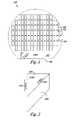
- FIG. 1an example silicon comprising semiconductor wafer 100 .
- the waferincludes a number of unsingulated die 102 for undergoing integrated circuit fabrication and processing thereupon.
- such wafers 100are provided with a registration mark, shown in this example as wafer edge 103 , which is used to orient the integrated circuit fabrication and processing steps in the ⁇ 110> direction.
- such wafers 100are also provided with a top surface 101 exposing the (100) crystalline plane of the silicon thereon.
- Embodiments of the present disclosureinvolve rotating the wafer 100 such that integrated circuit fabrication and processing are instead oriented along the ⁇ 100> direction of the silicon crystalline structure provided on the wafer 100 .
- FIG. 2is a three dimensional cross sectional view illustrating cuts oriented along different crystalline direction of the silicon comprising material.
- the three dimensional view of FIG. 2illustrate a top surface 202 having a (100) silicon crystal plane.
- FIG. 2illustrates a three dimensional cut 210 as could be made into the silicon comprising material of the wafer in the ⁇ 110> direction of silicon crystalline structure.
- FIG. 2additionally illustrates a three dimensional cut 220 as is made into the silicon comprising material of the wafer along the ⁇ 100> direction such that the walls, e.g., the surface 204 , also run along the ⁇ 100> direction and have a (100) silicon crystal plane.
- the wafere.g., wafer 100 shown in FIG. 1
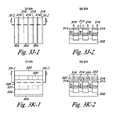
- FIGS. 3A-1 through 3 K- 2illustrate a NAND Flash process embodiment according to the present disclosure.
- FIG. 3A-1illustrates a top view of a portion of a memory die, e.g., as can be formed on a semiconductor wafer as shown in FIG. 1 .
- the illustrated portionis intended to represent that portion of a memory die whereupon a memory cell array is to be formed.
- the illustrated portioninclude a top surface 302 of single crystalline silicon having a (100) crystal plane.
- the illustrated surface 302can be etched to open the memory cell array while creating periphery shallow trench isolation (STI) on the die, as will be appreciated by one of ordinary skill in the art.
- FIG. 3A-2illustrates a side view cross section taken along-cut line 3 A- 2 reflecting the recessed single crystalline silicon 302 in the memory cell array portion of the die.
- STIperiphery shallow trench isolation
- FIG. 3B-1illustrates a top view of the portion of the die after a next sequence of processing steps.
- a fill of dielectric material 304is provided to the opened portions of the memory die.
- the dielectric fillis an STI oxide fill, e.g., using a dielectric such as TEOS.
- the fillhas been performed for the periphery of the array along with a subsequent planarization, e.g. chemical mechanical planarization (CMP).
- CMPchemical mechanical planarization
- FIG. 3B-2provides the cross-sectional side view taken along cut line 3 B- 2 showing the oxide layer 304 formed above the single crystalline silicon 302 .
- a hardmask 308is formed over the oxide layer 306 on the wafer, e.g., using photolithographic techniques.
- the hardmask 308is patterned to form lines oriented in the ⁇ 100> direction of the underlying single crystalline silicon. In various embodiments this can involve rotating a supporting wafer which has an original registration mark intended to orient processing steps in the ⁇ 110> direction such that the process sequence will instead orient the hardmask 308 along the ⁇ 100> direction of the underlying single crystalline silicon.
- FIG. 3C-2provides the cross-sectional side view taken along cut line 3 C- 2 .
- 3C-1 and 3 C- 2illustrate an optional additional dielectric layer, e.g., TiN layer, 306 which can be provided, e.g., using a chemical vapor deposition (CVD), to afford added smoothness and/or a sacrificial layer for removal later in the process flow.
- FIG. 3C-2thus illustrates a side view of the hardmask 308 patterned in the ⁇ 100> direction on the oxide layer 304 and an additional dielectric layer 306 .
- FIGS. 3D-1 and 3 D- 2illustrate a top view and a side view of the portion of the die after a next sequence of processing steps.
- the hardmask and oxide layer 306have been etched, e.g., using a wet etch, plasma etch, or other suitable technique, etc., to expose the single crystalline silicon 302 with lines for the NAND array patterned in the ⁇ 100> direction.
- what is shown in top view of FIG. 3D-1are lines of the sacrificial dielectric layer 306 and lines of the exposed single crystalline silicon 302 oriented along the ⁇ 100> direction of exposed single crystalline silicon 302 .
- 3D-2is the cross section taken along cut line 3 D- 2 illustrating the remaining sacrificial dielectric layer 306 on columns of oxide 304 and the exposed single crystalline silicon 302 underneath.
- the embodiments described hereinhave thus formed a number of trenches in the oxide dielectric material 304 having trench walls 305 in the ⁇ 100> direction relative to the exposed the single crystalline silicon 302 underneath.
- FIG. 3E-1the hardmask 308 and sacrificial dielectric layer 306 have been removed, e.g., using a selective etch, etc.
- the exposed surfacesare pre-cleaned before next epitaxially growing single crystalline silicon between trench walls 305 formed in the oxide dielectric layer 304 .
- FIG. 3E-2is a cross sectional view showing the trench walls 305 formed in the oxide dielectric layer 304 with the exposed single crystalline silicon 302 below and therebetween.
- the pre-cleanincludes exposing the single crystalline silicon 302 to a solution including a fluoride component, an oxidizing agent, and an inorganic acid.
- FIGS. 3F-1 and 3 F- 2illustrate a top view and a side view of the portion of the die after a next sequence of processing steps.
- single crystalline silicon 312has been epitaxially grown from the exposed single crystalline silicon 302 in the channels formed by the walls of the trenches 305 in the oxide dielectric material 304 .
- a pad oxide 310can then be grown, e.g., O 2 or H 2 O diffusion, and planarized or etched back to provide the structure shown in FIGS. 3F-1 and 3 F- 2 .
- the epitaxially grown single crystalline silicon 312is substantially free of dislocations.
- the low defectsenables STI scaling of NAND Flash stripes down as far as oxide may be patterned without the complication of spin on dielectric (SOD) or high density plasma (HDP) fill and densification at STI.
- FIGS. 3G-1 and 3 G- 2illustrate a top view and a side view of the portion of the die after a next sequence of processing steps.
- FIGS. 3G-1 and 3 G- 2implants to the cell array and array periphery work have been completed.
- Cell tunnel oxide 314is grown from the pad oxide 310 .
- the floating gate 316e.g., polysilicon, can next be deposited, e.g., by CVD, etc., and a dielectric layer, sacrificial oxide 318 applied thereover, e.g., by SOD.
- the structurecan then be planarized, e.g., by CMP, down to the original STI oxide level, e.g., top surface level of the oxide dielectric layer 304 , or optional sacrificial dielectric layer 306 , e.g., nitride cap, if one was applied.
- CMPCMP
- FIGS. 3I-1 and 3 I- 2the floating gate polysilicon 316 in the cell array can be recessed.
- the cell array structureis now appears in the top view illustration of FIG. 3I-1 and in the side view of FIG. 3I-2 taken along cut line 3 I- 2 .
- FIGS. 3J-1 and 3 J- 2the resulting structure is illustrated after the sacrificial oxide 318 has been removed and the oxide dielectric layer 304 has been leveled to beneath a top surface of the floating gates 316 .
- the cell array structureis now as appears in the top view illustration of FIG. 3J-1 and in the side view of FIG. 3J-2 taken along cut line 3 J- 2 .
- FIGS. 3K-1 and 3 K- 2the resulting NAND cell array structure is illustrated after a high vacuum oxide 320 is applied and a control gate material 322 is applied which can be patterned.
- the cell array structureis now appears in the top view illustration of FIG. 3K-1 and in the side view of FIG. 3K-2 taken along cut line 3 J- 2 .
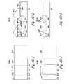
- FIGS. 4A-1 through 4 F- 2illustrates a dynamic random access memory (DRAM) process embodiment according to the present disclosure.
- FIG. 4A-1illustrates a top view of a portion of a memory die, e.g., as can be formed on a semiconductor wafer as shown in FIG. 1 . The illustrated portion is intended to represent that portion of a memory die whereupon a DRAM memory cell array is to be formed.
- a top surface of the wafercan be processed to include a top surface of single crystalline silicon having a (100) crystal plane.
- FIG. 4Ashows an embodiment in which strips of “Fins” 401 have been pattered into the silicon.
- One of ordinary skill in the artwill appreciate the manner in which the wafer can be masked, patterned, and etched to create strips of silicon Fins on the wafer. In previous approaches a wafer would undergo DRAM processing using a registration intended to orient the processing steps in the ⁇ 110> direction as shown in FIG. 1 .
- the waferis rotated relative to the original ⁇ 110> direction registration mark such that the wafer is oriented in the ⁇ 100> direction as shown by arrow 400 .
- the strips of single crystalline silicon Fins shown in FIGS. 4 A- 4 F- 2are oriented along the ⁇ 100> direction of the underlying single crystalline silicon.
- FIG. 4A-2provides the cross-sectional side view taken along cut line 4 A- 2 .
- FIG. 4A-2illustrates that a pad oxide layer 406 and a silicon-nitride layer 404 masking material are used and patterned before etching to form the strips of single crystalline silicon Fins 401 on the wafer.
- the pad oxide 406 and nitride layer 404can be deposited, for example, using CVD.
- a photolithographic etch processcan be employed as used for the STI formation.
- a light wet nitride etchcan be employed to reduce the nitride 404 critical dimension, e.g., from approximately 1.0 photolithographic feature (IF), above the single crystalline silicon Fins 401 and expose the single crystalline silicon along the nitride 404 .
- the example embodiment of FIG. 4A-1illustrates the single crystalline Fins 404 having a IF dimension with a 6F dimension between the single crystalline silicon Fins 401 .
- the patterncan be modified to achieve various single crystalline silicon channel dimensions as tied to the substrate of the wafer.
- FIGS. 4B-1 and 4 B- 2illustrate a top view and a side view of the portion of the die after a next sequence of processing steps.
- the structure of FIGS. 4A-1 and 4 A- 2has been patterned for the addition of a buried oxide (BOX) 408 which has been filled into the space between the single crystalline silicon Fins 401 and planarized, e.g., using CMP, as part of the STI formation process.
- the side view of FIG. 4B-2thus illustrates a cross sectional view of the structure taken along cut line 4 A- 2 in FIG. 4A-1 .
- FIG. 4A-2illustrates the BOX 408 between the single crystalline silicon Fins 401 formed in the single crystalline silicon surface 402 of the wafer.
- FIG. 4A-2illustrates the pad oxide 406 and the nitride 408 remaining on the top of the single crystalline silicon Fins 401 oriented in strips along the ⁇ 100> direction as well as on the top of the periphery to the DRAM memory cell array.
- the BOX 408 between the single crystalline silicon Fins 401 formed in the single crystalline silicon surface 402 of the wafereffectively provides isolation trenches.
- the BOX 408 embodiment in FIGS. 4B-1 and 4 B- 2is illustrated without the inclusion of a nitride liner thereto.
- FIGS. 4C-1 and 4 C- 2illustrate a top view and a side view of the portion of the die after a next sequence of processing steps.
- the BOX 408has been recessed to below a top surface 409 , as shown in FIG. 4D-2 , of the single crystalline silicon Fins 401 .
- the exposed single crystalline silicon surfacesare pre-cleaned before next epitaxially growing single crystalline silicon 410 between trench walls 412 formed from recessing the BOX 408 .
- the pre-cleanincludes exposing the single crystalline silicon of the trench walls 412 to the Fins 401 to a solution including a fluoride component, an oxidizing agent, and an inorganic acid.
- a solution including a fluoride component, an oxidizing agent, and an inorganic acidis provided in a copending, commonly assigned U.S. patent application entitled, “Wet Etch Suitable for Creating Square Cuts in Si and Resulting Structures”, Ser. No. 11/445,718, filed Jun. 2, 2006, which is incorporated in full herein.
- FIG. 4C-2illustrates a side view of the portion of the die after epitaxially growing the single crystalline silicon 410 from the trench walls 412 .
- the epitaxially grown single crystalline silicon 410is substantially free of dislocations. That is, due to the process of epitaxially growing the single crystalline silicon 410 between dielectric walls, e.g., the nitride 404 , oriented in the ⁇ 100> direction relative to the exposed single crystalline silicon 402 any dislocations are pinned at the semiconductor/dielectric interface, e.g., along nitride walls 404 .
- the low defectsenable DRAM access transistors to be formed, as described further below, in the epitaxial single crystalline silicon 410 .
- thisachieves reduced stress in the active area of small geometry DRAM material to enable low defect retrograde access fins or recessed access devices (RADs) and Fin field effect transistor (FinFET) structures.
- the epitaxial single crystalline silicon 410 materialcan be cut across the trenches 412 by patterning and etching to enable isolation of DRAM or NOR devices using, for example, STI techniques in one direction of isolation.
- FIG. 4C-1illustrates the epitaxially grown single crystalline silicon 410 formed only between trench walls 412 of the single crystalline silicon Fins 410 .
- the cross sectional view of FIG. 4C-2illustrates that embodiments are not so limited and that the epitaxially grown single crystalline silicon may be grown to connect and form overtop the nitride 404 .
- FIGS. 4D-1 and 4 D- 2illustrate a top view and a side view embodiment of the portion of the die after a next sequence of processing steps.
- the epitaxially grown single crystalline silicon 410is planarized, e.g., by CMP, to the nitride 404 .
- the exposed nitride 404 and pad oxide 406can next be removed, e.g., by using a wet strip, etc., to reveal the structure shown in the cross sectional view of FIG. 4D-2 .
- an STI flow processcan next be followed to continue with forming DRAM cells.
- FIGS. 4E-1 and 4 E- 2illustrate the structure after a next sequence of processing steps. As represented by the top view and side view embodiment of FIGS. 4E-1 and 4 E- 2 another pad oxide layer and another nitride layer can be deposited and patterned for the formation of additional trench isolation 412 and to define cell array active areas 414 and peripheral active areas 402 .
- FIG. 4E-2is a cross sectional view illustrating the same taken along 4 E- 2 . A selective wet etch can be performed to remove the nitride and an HF clean can be performed to remove the pad oxide.
- FIGS. 4E-1 and 4 E- 2illustrate both the exposed single crystalline silicon epitaxial regions 412 and the single crystalline silicon layer 402 of the wafer.
- FIGS. 4F-1 and 4 F- 2illustrate the structure after a next sequence of processing steps.
- Embodiments for integrated circuitry in fabrication of DRAM cell array and peripheral gateis represented by the top view and side view embodiment of FIGS. 4F-1 and 4 F- 2 .
- the cross sectional view shown in FIG. 4F-2illustrates a number of gate structures 415 - 1 , 415 - 2 , 415 - 3 , . . . , 415 -N for the cell array and the peripheral gate 415 -P.
- each of the gate structures 415includes a gate dielectric layer 416 , a conductively doped polysilicon region 417 , conductive metal or metal silicide region 418 , and insulative caps 420 . Electrically insulative sidewall spacers (not shown) are received about the respective gate structures. Electrically insulative material is illustrated at 408 (trench isolation BOX) and 412 (STI oxide for isolating adjacent devices) as the same have been described above.
- the epitaxially grown single crystalline silicon 410is illustrated as forming a source region 421 and a channel region 422 .
- the shared drain region 423is illustrated as formed from the single crystalline silicon 402 of the wafer.
- the cell array structureis now as appears in the top view illustration of FIG. 4F-1 and in the side view of FIG. 4F-2 taken along cut line 4 F- 2 .
- electrically conductive contactscan be formed to connect with the source and drain regions, respectively, and the DRAM fabrication process continued and completed as suitable for particular implementations. As such more detail is not provided hereafter.
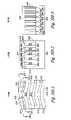
- FIGS. 5A-1 through 5 K- 3 - 2illustrates a pseudo silicon on insulator (PSOI) involving epitaxially grown single crystalline silicon process embodiment involving epitaxially grown single crystalline silicon according to the present disclosure.
- FIG. 5A-1illustrates a top view of a portion of a memory die, e.g., as can be formed on a semiconductor wafer as shown in FIG. 1 . The illustrated portion is intended to represent that portion of a memory die whereupon a DRAM memory cell array is to be formed.
- a top surface of the wafercan be processed to include a top surface of single crystalline silicon having a (100) crystal plane.
- FIG. 5Ashows an embodiment in which photo resist lines orthogonal to planned epitaxially single crystal silicon overgrowth in the ⁇ 100> direction is planned.
- One of ordinary skill in the artwill appreciate the manner in which the wafer can be masked and patterned. In previous approaches a wafer would undergo DRAM processing using a registration intended to orient the processing steps in the ⁇ 110> direction as shown in FIG. 1 .
- the waferis rotated relative to the original ⁇ 110> direction registration mark such that the wafer is oriented in the ⁇ 100> direction as shown by arrow 500 .
- FIG. 5A-2provides the cross-sectional side view taken along cut line 5 A- 2 .
- FIG. 5A-2illustrates that a silicon-nitride 504 hardmask layer has been applied beneath the patterned strips of photo resist lines 506 in the ⁇ 100> direction and over the underlying substrate 502 of the wafer.
- the substrate 502 portion showncan include bulk semiconductive silicon comprising material and may include a layer of single crystalline silicon.
- FIGS. 5B-1 and 5 B- 2illustrate a top view and a side view of the portion of the die after a next sequence of processing steps.
- the structure of FIGS. 5A-1 and 5 A- 2has undergone an anisotropic etch to etch into the nitride hardmask 504 and the single crystalline silicon 502 .
- the cross sectional view of FIG. 5B-2illustrates the trench walls 505 formed in the ⁇ 100> direction in the single crystalline silicon 502 from the etch process above.
- the trenchescan be formed to a depth in the range of 500 to 3000 Angstroms. Embodiments, however, are not limited to this example.
- a width to the trenchescan be patterned to provide a particular dimension to the trenches.
- photolithography techniqueseach have a minimum pitch below which a particular photolithographic technique cannot reliably form features.
- Pitchis defined as the distance between an identical point in two neighboring features. These features are typically defined by openings in, and spaced from each other by, a material, such as an insulator or conductor. As a result, pitch can be viewed as the sum of the width of a feature and of the width of the space separating that feature from a neighboring feature.
- pitch doublingis one method for extending the capabilities of photolithographic techniques beyond their minimum pitch and can be used in forming the trenches shown in various embodiments.
- One example method for the sameis described in U.S. Pat. No. 5,328,810, issued to Lowrey et al., the entire disclosure of which is incorporated herein by reference.
- pitch “doubling”the reduction in pitch
- pitch “multiplication”the reduction in pitch
- pitch “multiplication” of pitch by a certain factoractually involves reducing the pitch by that factor.
- This terminologyis retained herein. Note that by forming spacers upon spacers, the definable feature size can be further decreased.
- pitch multiplicationrefers to the process generally, regardless of the number of times the spacer formation process is employed.
- the exposed surfacesare pre-cleaned before next epitaxially growing single crystalline silicon from the exposed portions of single crystalline silicon on the trench walls 505 .
- the pre-cleanincludes exposing the single crystalline silicon 502 to a solution including a fluoride component, an oxidizing agent, and an inorganic acid.
- exposing the single crystalline silicon 502 to a solution including a fluoride component, an oxidizing agent, and an inorganic acidis provided in a copending, commonly assigned U.S. patent application entitled, “Wet Etch Suitable for Creating Square Cuts in Si and Resulting Structures”, Ser. No. 11/445,718, filed Jun. 2, 2006, which is incorporated in full herein.
- FIGS. 5D-1 and 5 D- 2illustrate a top view and a side view of the portion of the die after a next sequence of processing steps.
- single crystalline siliconhas been epitaxially grown from the exposed single crystalline silicon 502 with merging fronts 510 .
- an optional polysilicon layer 512is applied over the top, e.g., via CVD.
- the epitaxial overgrowth 510 above the dielectric fins, e.g., nitride spacers 508is substantially free of dislocations.
- the dielectric(here, nitride spacers 508 ) can be recessed to allow epitaxial silicon growth 510 over the gaps 509 which will merge (100) single crystalline silicon planes.
- this embodimentallows PSOI DRAM devices without using two (2) CMPs.
- FIGS. 5G-1illustrates a top view of the portion of the die after the next sequence of processing steps.
- FIGS. 5G-2 and 5 G- 3illustrate cross sectional views taken along cut lines 5 G- 2 and 5 G- 3 , respectively, shown in FIG. 5G-1 .
- the nitride 514 and epitaxially grown single crystalline silicon 510have been etched using a plasma dry etch, e.g., using a Br, Ar base gas recipe, to define islands 511 as shown by contrasting cross sectional views of FIG. 5G-2 and 5 G- 3 along those respective cut lines from 5 G- 1 as well as undercut source/drain regions 509 .
- the nitride spacers 508 shown in FIG. 5G-3can optionally be removed by a dry etch or a wet etch.
- FIGS. 5H-1illustrates a top view of the portion of the die after the next sequence of processing steps.
- FIGS. 5H-2 and 5 H- 3illustrate cross sectional views taken along cut lines 5 H- 2 and 5 H- 3 , respectively, shown in FIG. 5H-1 .
- a spin on dielectric (SOD) oxide deposition 518 and planarization, e.g. via CMP,have been performed to complete the STI sequence.
- SODspin on dielectric
- the structureis now as appears in FIGS. 5H-1 , 5 H- 2 , and 5 H- 3 showing oxide 518 in the undercut source/drain regions in the view of 5 H- 2 and in isolation regions outside of the active regions of the devices to be formed in the view of 5 H- 3 .
- FIGS. 5I-1illustrates a top view of the portion of the die after the next sequence of processing steps.
- FIGS. 5I-2 and 5 I- 3illustrate cross sectional views taken along cut lines 5 I- 2 and 5 I- 3 , respectively, shown in FIG. 5I-1 .
- the nitride 514 from FIGS. 5H-1 , 5 H- 2 , and 5 H- 3has been removed, e.g., using a nitride wet etch or other suitable technique.
- FIGS. 5J-1illustrates a top view of the portion of the die after the next sequence of processing steps.
- FIGS. 5J-2 and 5 J- 3illustrate cross sectional views taken along cut lines 5 J- 2 and 5 J- 3 , respectively, shown in FIG. 5J-1 .
- the structureillustrates a DRAM device array having gates 519 over the silicon island body ties 511 .
- the gates 519 and source/drain regionscan be formed, for example, according to the process embodiment described above in connection with FIGS. 4F-1 and 4 F- 2 .
- each of the gates 519can be formed to include a gate dielectric layer 520 , a conductively doped polysilicon region 521 , conductive metal or metal silicide region 522 , and insulative caps 523 .
- the gates 519are thus formed over the epitaxially grown single crystalline silicon 510 which serves as a channel region connected to island 511 body ties as shown in cross sectional view 5 J- 2 and pass over the oxide isolation material 518 outside of the active areas of the DRAM cells as shown in the cross sectional view of 5 J- 3 .
- the source/drain regionsare thus formed in the epitaxially grown single crystalline silicon 510 undercut by the oxide isolation material 518 as shown in the cross sectional view of FIG. 5J-2 .
- Electronic system 600includes an external processor 620 , e.g., a memory controller or host processor, electrically connected to memory device 602 for memory accessing.
- the memory device 602receives control signals from the processor 620 over a control link 622 .
- the memory cellsare used to store data that are accessed via a data (DQ) link 624 .
- Address signalsare received via an address link 626 that are decoded at address decoder 606 to access the memory array 604 .
- Address buffer circuit 616latches the address signals.
- the memory cellsare accessed in response to the control signals and the address signals.
- FIG. 7is a functional block diagram of a memory module 700 having at least one memory device having structures formed in epitaxially grown silicon according to the embodiments of the present disclosure.
- Memory module 700is illustrated as a memory card, although the concepts discussed with reference to memory module 700 are applicable to other types of removable or portable memory (e.g., USB flash drives) and are intended to be within the scope of “memory module” as used herein.
- memory modulee.g., USB flash drives
- FIG. 7one example form factor is depicted in FIG. 7 , these concepts are applicable to other form factors as well.
- memory module 700will include a housing 705 to enclose one or more memory devices 710 , though such a housing is not essential to all devices or device applications.
- the housing 705includes one or more contacts 715 for communication with a host device. Examples of host devices include digital cameras, digital recording and playback devices, PDAs, personal computers, memory card readers, interface hubs and the like.
- the contacts 715are in the form of a standardized interface. For example, with a USB flash drive, the contacts 715 might be in the form of a USB Type-A male connector.
- the contacts 715are in the form of a semi-proprietary interface, such as might be found on CompactFlashTM memory cards licensed by SanDisk Corporation, Memory StickTM memory cards licensed by Sony Corporation, SD Secure DigitalTM memory cards licensed by Toshiba Corporation and the like. In general, however, contacts 715 provide an interface for passing control, address and/or data signals between the memory module 700 and a host having compatible receptors for the contacts 715 .
- the memory module 700may optionally include additional circuitry 720 , which may be one or more integrated circuits and/or discrete components.
- the additional circuitry 720may include a memory controller for controlling access across multiple memory devices 710 and/or for providing a translation layer between an external host and a memory device 710 .
- a memory controllercould selectively couple an I/O connection (not shown in FIG. 7 ) of a memory device 710 to receive the appropriate signal at the appropriate I/O connection at the appropriate time or to provide the appropriate signal at the appropriate contact 715 at the appropriate time.
- the communication protocol between a host and the memory module 700may be different than what is required for access of a memory device 710 .
- a memory controllercould then translate the command sequences received from a host into the appropriate command sequences to achieve the desired access to the memory device 710 .
- Such translationmay further include changes in signal voltage levels in addition to command sequences.
- the additional circuitry 720may further include functionality unrelated to control of a memory device 710 such as logic functions as might be performed by an ASIC. Also, the additional circuitry 720 may include circuitry to restrict read or write access to the memory module 700 , such as password protection, biometrics or the like. The additional circuitry 720 may include circuitry to indicate a status of the memory module 700 . For example, the additional circuitry 720 may include functionality to determine whether power is being supplied to the memory module 700 and whether the memory module 700 is currently being accessed, and to display an indication of its status, such as a solid light while powered and a flashing light while being accessed. The additional circuitry 720 may further include passive devices, such as decoupling capacitors to help regulate power requirements within the memory module 700 .
- Memory cell structuresincluding PSOIs, NANDs, NORs, FinFETs, etc., and methods of fabrication have been described that include a method of epitaxial silicon growth.
- the methodincludes providing a silicon layer on a substrate.
- a dielectric layeris provided on the silicon layer.
- a trenchis formed in the dielectric layer to expose the silicon layer, the trench having trench walls in the ⁇ 100> direction.
- the methodincludes epitaxially growing silicon between trench walls formed in the dielectric layer.
- the single crystalline siliconis grown substantially free of dislocations.
- the various techniques described hereinprovide a process of epitaxially growing the single crystalline silicon oriented in the ⁇ 100> direction relative to the underlying silicon crystalline structures such that any defects are pinned at semiconductor/dielectric interfaces, e.g., along trench walls.
- such epitaxially grown single crystalline siliconcan be grown substantially free of dislocations at multiple elevations and then overgrowth methods used to create defect free silicon over silicon (SOS), hence stacking devices, e.g., transistors at multiple levels.
- SOSdefect free silicon over silicon
- Other devicessuch as pass gates or local amplifiers atop contacts which contact lower level gate and source/drain regions could similarly be constructed using the embodiments described herein.
- building micro electro mechanical (MEM) structures or optical electrical devices out of silicon on (100) crystal planesmay be enabled by the ability to put down substantially defect free epitaxially grown single crystalline silicon as described herein.
Landscapes
- Engineering & Computer Science (AREA)
- Manufacturing & Machinery (AREA)
- Physics & Mathematics (AREA)
- Condensed Matter Physics & Semiconductors (AREA)
- General Physics & Mathematics (AREA)
- Computer Hardware Design (AREA)
- Microelectronics & Electronic Packaging (AREA)
- Power Engineering (AREA)
- Chemical & Material Sciences (AREA)
- Materials Engineering (AREA)
- Semiconductor Memories (AREA)
- Non-Volatile Memory (AREA)
Abstract
Description
- The present disclosure relates generally to semiconductor devices and, more particularly, to semiconductor devices formed from epitaxial silicon growth.
- Higher performance, lower cost, increased miniaturization of semiconductor components, and greater packing density of integrated circuit are ongoing goals of the semiconductor industry. Integrated circuit (IC) processing/fabrication is used to produce transistors having various structures including recessed access device (RAD), Fin field effect transistor (FinFET), pseudo silicon on insulator (PSOI), and nanowire, etc., for use in dynamic random access memory (DRAM), NOR and NAND Flash memory, and floating body memory, among other semiconductor devices.
- IC processing for memory and other semiconductor devices are currently performed on silicon wafers having a top surface of (100) crystal plane. This surface structures was chosen over the previously used (111) crystal plane because of its comparatively low surface state density on thermally oxidized surfaces. For example, in the diamond lattice of silicon the (111) plane is more densely packed than the (100) plane, and thus etch rates of {111} orientated surfaces are expected to be lower than those with {100} orientation. Bonding orientation of the different planes also contributes to etchant selectivity to exposed planes. One etchant that exhibits such orientation dependent etching properties consists of a mixture of KOH and isopropyl alcohol. For example, such a mixture may etch about one hundred times faster along (100) planes than along (111) planes.
- Various chemistries have been used to etch silicon. For example, both single crystal and polycrystalline silicon may be wet etched in mixtures of nitric acid (HNO3) and hydrofluoric acid (HF). With use of such etchants, the etching may be isotropic. The reaction is initiated by the HNO3, which forms a layer of silicon dioxide on the silicon, and the HF dissolves the silicon oxide away. In some cases, water is used to dilute the etchant, with acetic acid (CH3COOH) used as a buffering agent.
- Wafers having the top surface of {100} crystal plane are currently provided with a registration mark in the orthogonal <110> direction. IC processing of the wafer is then performed using this <110> registration mark. Hence, masks are aligned along the <110> direction.
- Integrated circuitry can be fabricated relative to one or both of bulk semiconductor substrates, such as silicon wafers, and semiconductor on insulator (SOI) substrates. SOI forms a semiconductor layer, e.g., silicon, onto an insulator, e.g., silicon dioxide. One method of forming SOI circuitry, at least in part, includes epitaxially growing single crystalline silicon electively from a single crystalline surface. Unfortunately in some instances epitaxially grown silicon tends to form crystalline defects, known as dislocations and stacking faults, which can result in undesired leakage within or between the resulting fabricated devices.
FIG. 1 illustrates an example silicon comprising semiconductor wafer.FIG. 2 is a three dimensional cross sectional view illustrating cuts oriented along different crystalline direction of the silicon comprising material.FIGS. 3A-1 through3K-2 illustrate a NAND Flash process embodiment according to the present disclosure.FIGS. 4A-1 through4F-2 illustrate a dynamic random access memory (DRAM) process embodiment according to the present disclosure.FIGS. 5A-1 through5J-3 illustrates a pseudo silicon on insulator (PSOI) involving epitaxially grown single crystalline silicon process embodiment involving epitaxially grown single crystalline silicon according to the present disclosure.FIG. 6 illustrates an example of an embodiment of an electronic system which includes structures formed in epitaxially grown silicon according to the embodiments of the present disclosure.FIG. 7 is a functional block diagram of a memory module having at least one memory device having structures formed in epitaxially grown silicon according to the embodiments of the present disclosure.- Methods, devices, and arrays are described which include semiconductor devices formed from epitaxially grown silicon. Various embodiments reduce dislocations and/or defects in the epitaxial (“epi”) silicon and resulting devices, arrays, etc.
- One method embodiment includes providing a silicon layer on a substrate, the silicon having a top surface with a (100) crystal plane. A dielectric layer is provided on the silicon layer. As one example, providing a dielectric layer can include performing a high density plasma (HDP) oxide deposition on the silicon layer. A trench is formed in the dielectric layer to expose the silicon layer, the trench having trench walls in the <100> direction. The method includes epitaxially growing silicon between trench walls formed in the dielectric layer.
- In some embodiments, the silicon layer is provided on a wafer having a registration mark in the <110> direction and the wafer is rotated such that the trench walls will be formed in the <100> direction, e.g., the wafer is rotated forty five degrees so that a mask is aligned in the <100> direction. Alternatively, the registration mark can be provided in the orthogonal <010> direction. In some embodiments, a pre-clean which includes exposing the silicon layer and the trench walls to a solution including a fluoride component, an oxidizing agent, and an inorganic acid, is performed prior to epitaxially growing silicon between the trench walls.
- As used herein the terms “wafer” and “substrate” may include a number of semiconductor-based structures that have an exposed semiconductor surface. Structure can be understood to include silicon, silicon-on-insulator (SOI), silicon-on sapphire (SOS), doped, and undoped semiconductors. In addition, structure can be understood to include epitaxial layers of silicon supported by a base semiconductor foundation. The base semiconductor foundation is typically the lowest layer of silicon material on a wafer or a silicon layer deposited on another material.
- The semiconductor need not be silicon-based. For example, the semiconductor can be silicon-germanium, germanium, or gallium-arsenide. When reference is made to “wafer” and “substrate” in the following description, previous process steps may have been utilized to form regions or junctions in or on the semiconductor structure and/or foundation. When reference is made to a substrate assembly, various process steps may have been previously used to fomm or define regions, junctions, various structures or features, and openings such as capacitor plates or barriers for capacitors.
- As used herein, “layer” can refer to a layer formed on a substrate using a deposition process, e.g., plasma and/or chemical vapor deposition (CVD) process. The term “layer” is meant to include layers specific to the semiconductor industry, such as “barrier layer”, “dielectric layer”, and “conductive layer”. The term “layer” is also meant to include layers found in technology outside of semiconductor technology, such as coatings on glass.
- In the Figures, the first digit of a reference number refers to the Figure in which it is used, while the remaining two digits of the reference number refer to the same or equivalent parts of embodiment(s) of the present disclosure used throughout the several figures of the drawing. The scaling of the figures does not represent precise dimensions and/or dimensional ratios of the various elements illustrated herein.
FIG. 1 an example silicon comprisingsemiconductor wafer 100. The wafer includes a number of unsingulated die102 for undergoing integrated circuit fabrication and processing thereupon. As shown inFIG. 1 ,such wafers 100 are provided with a registration mark, shown in this example aswafer edge 103, which is used to orient the integrated circuit fabrication and processing steps in the <110> direction. As shown,such wafers 100 are also provided with atop surface 101 exposing the (100) crystalline plane of the silicon thereon. Embodiments of the present disclosure, which are discussed more below, involve rotating thewafer 100 such that integrated circuit fabrication and processing are instead oriented along the <100> direction of the silicon crystalline structure provided on thewafer 100.FIG. 2 is a three dimensional cross sectional view illustrating cuts oriented along different crystalline direction of the silicon comprising material. The three dimensional view ofFIG. 2 illustrate atop surface 202 having a (100) silicon crystal plane.FIG. 2 illustrates a threedimensional cut 210 as could be made into the silicon comprising material of the wafer in the <110> direction of silicon crystalline structure.FIG. 2 additionally illustrates a threedimensional cut 220 as is made into the silicon comprising material of the wafer along the <100> direction such that the walls, e.g., thesurface 204, also run along the <100> direction and have a (100) silicon crystal plane. According to the embodiments described below, the wafer, e.g.,wafer 100 shown inFIG. 1 , is oriented such that integrated circuit fabrication and processing is performed with cuts being made into the silicon comprising material of the wafer to form walls in the <100> crystal direction versus the <110> crystal direction.FIGS. 3A-1 through3K-2 illustrate a NAND Flash process embodiment according to the present disclosure.FIG. 3A-1 illustrates a top view of a portion of a memory die, e.g., as can be formed on a semiconductor wafer as shown inFIG. 1 . The illustrated portion is intended to represent that portion of a memory die whereupon a memory cell array is to be formed. The illustrated portion include atop surface 302 of single crystalline silicon having a (100) crystal plane. In the embodiment ofFIG. 3A-1 the illustratedsurface 302 can be etched to open the memory cell array while creating periphery shallow trench isolation (STI) on the die, as will be appreciated by one of ordinary skill in the art. Hence,FIG. 3A-2 illustrates a side view cross section taken along-cut line 3A-2 reflecting the recessed singlecrystalline silicon 302 in the memory cell array portion of the die.FIG. 3B-1 illustrates a top view of the portion of the die after a next sequence of processing steps. InFIG. 3B-1 a fill ofdielectric material 304 is provided to the opened portions of the memory die. In various embodiments the dielectric fill is an STI oxide fill, e.g., using a dielectric such as TEOS. InFIGS. 3B-1 and3B-2 the fill has been performed for the periphery of the array along with a subsequent planarization, e.g. chemical mechanical planarization (CMP). In the process that portion of the memory die whereupon a memory cell array is to be formed can also be concurrently filled withoxide 304 and planarized.FIG. 3B-2 provides the cross-sectional side view taken alongcut line 3B-2 showing theoxide layer 304 formed above the singlecrystalline silicon 302.- In
FIG. 3C-1 ahardmask 308 is formed over theoxide layer 306 on the wafer, e.g., using photolithographic techniques. According to embodiments of the present disclosure, thehardmask 308 is patterned to form lines oriented in the <100> direction of the underlying single crystalline silicon. In various embodiments this can involve rotating a supporting wafer which has an original registration mark intended to orient processing steps in the <110> direction such that the process sequence will instead orient thehardmask 308 along the <100> direction of the underlying single crystalline silicon.FIG. 3C-2 provides the cross-sectional side view taken alongcut line 3C-2.FIGS. 3C-1 and3C-2 illustrate an optional additional dielectric layer, e.g., TiN layer,306 which can be provided, e.g., using a chemical vapor deposition (CVD), to afford added smoothness and/or a sacrificial layer for removal later in the process flow.FIG. 3C-2 thus illustrates a side view of thehardmask 308 patterned in the <100> direction on theoxide layer 304 and an additionaldielectric layer 306. FIGS. 3D-1 and3D-2 illustrate a top view and a side view of the portion of the die after a next sequence of processing steps. InFIGS. 3D-1 and3D-2 the hardmask andoxide layer 306 have been etched, e.g., using a wet etch, plasma etch, or other suitable technique, etc., to expose the singlecrystalline silicon 302 with lines for the NAND array patterned in the <100> direction. Hence, what is shown in top view ofFIG. 3D-1 are lines of thesacrificial dielectric layer 306 and lines of the exposed singlecrystalline silicon 302 oriented along the <100> direction of exposed singlecrystalline silicon 302.FIG. 3D-2 is the cross section taken alongcut line 3D-2 illustrating the remainingsacrificial dielectric layer 306 on columns ofoxide 304 and the exposed singlecrystalline silicon 302 underneath. The embodiments described herein have thus formed a number of trenches in theoxide dielectric material 304 havingtrench walls 305 in the <100> direction relative to the exposed the singlecrystalline silicon 302 underneath.- In
FIG. 3E-1 thehardmask 308 andsacrificial dielectric layer 306 have been removed, e.g., using a selective etch, etc. According to various embodiments the exposed surfaces are pre-cleaned before next epitaxially growing single crystalline silicon betweentrench walls 305 formed in theoxide dielectric layer 304.FIG. 3E-2 is a cross sectional view showing thetrench walls 305 formed in theoxide dielectric layer 304 with the exposed singlecrystalline silicon 302 below and therebetween. In various embodiments the pre-clean includes exposing the singlecrystalline silicon 302 to a solution including a fluoride component, an oxidizing agent, and an inorganic acid. One example of exposing the singlecrystalline silicon 302 to a solution including a fluoride component, an oxidizing agent, and an inorganic acid is provided in a copending, commonly assigned U.S. patent application entitled, “Wet Etch Suitable for Creating Square Cuts in Si and Resulting Structures”, Ser. No. 11/445,718, filed Jun. 2, 2006, which is incorporated in full herein. FIGS. 3F-1 and3F-2 illustrate a top view and a side view of the portion of the die after a next sequence of processing steps. InFIGS. 3F-1 and3F-2 singlecrystalline silicon 312 has been epitaxially grown from the exposed singlecrystalline silicon 302 in the channels formed by the walls of thetrenches 305 in theoxide dielectric material 304. Apad oxide 310 can then be grown, e.g., O2or H2O diffusion, and planarized or etched back to provide the structure shown inFIGS. 3F-1 and3F-2. According to the process embodiments described herein the epitaxially grown singlecrystalline silicon 312 is substantially free of dislocations. That is, due to the process of epitaxially growing the singlecrystalline silicon 312 betweendielectric walls 304 oriented in the <100> direction relative to the exposed singlecrystalline silicon 302 any dislocations are pinned at the semiconductor/dielectric interface, e.g., alongtrench walls 305. Thus, according to this example embodiment, the low defects enables STI scaling of NAND Flash stripes down as far as oxide may be patterned without the complication of spin on dielectric (SOD) or high density plasma (HDP) fill and densification at STI. Theoxide fins 304 created here can be approximately 20 nanometers (nm) wide which will allow STI scaling down to a feature size of 20 nm (F=20 nm).- In contrast, other process flows have tackled epitaxially growing single crystalline silicon over geometric features in silicon (Si) or silicon/germanium (Si/Ge) but these works have all directed their attention to dislocations being pinned at interfaces of the semiconductors. One example of this is provided in a copending, commonly assigned U.S. patent application entitled, “Integrated Circuits and Methods of Forming a Field Effect Transistor”, application Ser. No. 11/076,774, filed Mar. 10, 2005, and which is incorporated in full herein.
FIGS. 3G-1 and3G-2 illustrate a top view and a side view of the portion of the die after a next sequence of processing steps. InFIGS. 3G-1 and3G-2 implants to the cell array and array periphery work have been completed.Cell tunnel oxide 314 is grown from thepad oxide 310. The floatinggate 316, e.g., polysilicon, can next be deposited, e.g., by CVD, etc., and a dielectric layer,sacrificial oxide 318 applied thereover, e.g., by SOD.- As shown in
FIGS. 3H-1 and3H-2, the structure can then be planarized, e.g., by CMP, down to the original STI oxide level, e.g., top surface level of theoxide dielectric layer 304, or optional sacrificialdielectric layer 306, e.g., nitride cap, if one was applied. - In
FIGS. 3I-1 and3I-2, the floatinggate polysilicon 316 in the cell array can be recessed. The cell array structure is now appears in the top view illustration ofFIG. 3I-1 and in the side view ofFIG. 3I-2 taken along cut line3I-2. - In
FIGS. 3J-1 and3J-2, the resulting structure is illustrated after thesacrificial oxide 318 has been removed and theoxide dielectric layer 304 has been leveled to beneath a top surface of the floatinggates 316. The cell array structure is now as appears in the top view illustration ofFIG. 3J-1 and in the side view ofFIG. 3J-2 taken alongcut line 3J-2. - In
FIGS. 3K-1 and3K-2, the resulting NAND cell array structure is illustrated after ahigh vacuum oxide 320 is applied and acontrol gate material 322 is applied which can be patterned. The cell array structure is now appears in the top view illustration ofFIG. 3K-1 and in the side view ofFIG. 3K-2 taken alongcut line 3J-2. FIGS. 4A-1 through4F-2 illustrates a dynamic random access memory (DRAM) process embodiment according to the present disclosure.FIG. 4A-1 illustrates a top view of a portion of a memory die, e.g., as can be formed on a semiconductor wafer as shown inFIG. 1 . The illustrated portion is intended to represent that portion of a memory die whereupon a DRAM memory cell array is to be formed. As part of the processing a top surface of the wafer can be processed to include a top surface of single crystalline silicon having a (100) crystal plane.- The top view illustrated in
FIG. 4A shows an embodiment in which strips of “Fins”401 have been pattered into the silicon. One of ordinary skill in the art will appreciate the manner in which the wafer can be masked, patterned, and etched to create strips of silicon Fins on the wafer. In previous approaches a wafer would undergo DRAM processing using a registration intended to orient the processing steps in the <110> direction as shown inFIG. 1 . - According to embodiments of the present disclosure, however, the wafer is rotated relative to the original <110> direction registration mark such that the wafer is oriented in the <100> direction as shown by
arrow 400. In the embodiments described herein, it is while the wafer is oriented in the <100> direction that the top surface of the wafer is masked, patterned, and etched to create the strips ofsilicon Fins 401 on the wafer. As such, the strips of single crystalline silicon Fins shown in FIGS.4A-4F-2 are oriented along the <100> direction of the underlying single crystalline silicon. FIG. 4A-2 provides the cross-sectional side view taken along cut line4A-2.FIG. 4A-2 illustrates that apad oxide layer 406 and a silicon-nitride layer 404 masking material are used and patterned before etching to form the strips of singlecrystalline silicon Fins 401 on the wafer. Thepad oxide 406 andnitride layer 404 can be deposited, for example, using CVD. A photolithographic etch process can be employed as used for the STI formation. In various embodiments a light wet nitride etch can be employed to reduce thenitride 404 critical dimension, e.g., from approximately 1.0 photolithographic feature (IF), above the singlecrystalline silicon Fins 401 and expose the single crystalline silicon along thenitride 404. The example embodiment ofFIG. 4A-1 illustrates the singlecrystalline Fins 404 having a IF dimension with a 6F dimension between the singlecrystalline silicon Fins 401. However, as the reader will appreciate the pattern can be modified to achieve various single crystalline silicon channel dimensions as tied to the substrate of the wafer.FIGS. 4B-1 and4B-2 illustrate a top view and a side view of the portion of the die after a next sequence of processing steps. As shown inFIGS. 4B-1 and4B-2 the structure ofFIGS. 4A-1 and4A-2 has been patterned for the addition of a buried oxide (BOX)408 which has been filled into the space between the singlecrystalline silicon Fins 401 and planarized, e.g., using CMP, as part of the STI formation process. The side view ofFIG. 4B-2 thus illustrates a cross sectional view of the structure taken along cut line4A-2 inFIG. 4A-1 .FIG. 4A-2 illustrates theBOX 408 between the singlecrystalline silicon Fins 401 formed in the singlecrystalline silicon surface 402 of the wafer.FIG. 4A-2 illustrates thepad oxide 406 and thenitride 408 remaining on the top of the singlecrystalline silicon Fins 401 oriented in strips along the <100> direction as well as on the top of the periphery to the DRAM memory cell array. TheBOX 408 between the singlecrystalline silicon Fins 401 formed in the singlecrystalline silicon surface 402 of the wafer effectively provides isolation trenches. TheBOX 408 embodiment inFIGS. 4B-1 and4B-2 is illustrated without the inclusion of a nitride liner thereto.FIGS. 4C-1 and4C-2 illustrate a top view and a side view of the portion of the die after a next sequence of processing steps. InFIGS. 4C-1 and4C-2 theBOX 408 has been recessed to below atop surface 409, as shown inFIG. 4D-2 , of the singlecrystalline silicon Fins 401. According to various embodiments of the present disclosure, the exposed single crystalline silicon surfaces are pre-cleaned before next epitaxially growing singlecrystalline silicon 410 betweentrench walls 412 formed from recessing theBOX 408. In various embodiments the pre-clean includes exposing the single crystalline silicon of thetrench walls 412 to theFins 401 to a solution including a fluoride component, an oxidizing agent, and an inorganic acid. One example of exposing the single crystalline silicon of thetrench walls 412 to a solution including a fluoride component, an oxidizing agent, and an inorganic acid is provided in a copending, commonly assigned U.S. patent application entitled, “Wet Etch Suitable for Creating Square Cuts in Si and Resulting Structures”, Ser. No. 11/445,718, filed Jun. 2, 2006, which is incorporated in full herein.FIG. 4C-2 illustrates a side view of the portion of the die after epitaxially growing the singlecrystalline silicon 410 from thetrench walls 412. According to the process embodiments described herein the epitaxially grown singlecrystalline silicon 410 is substantially free of dislocations. That is, due to the process of epitaxially growing the singlecrystalline silicon 410 between dielectric walls, e.g., thenitride 404, oriented in the <100> direction relative to the exposed singlecrystalline silicon 402 any dislocations are pinned at the semiconductor/dielectric interface, e.g., alongnitride walls 404. Thus, according to this example embodiment, the low defects enable DRAM access transistors to be formed, as described further below, in the epitaxial singlecrystalline silicon 410. In various embodiments, this achieves reduced stress in the active area of small geometry DRAM material to enable low defect retrograde access fins or recessed access devices (RADs) and Fin field effect transistor (FinFET) structures. As the reader will appreciate, the epitaxial singlecrystalline silicon 410 material can be cut across thetrenches 412 by patterning and etching to enable isolation of DRAM or NOR devices using, for example, STI techniques in one direction of isolation.- In contrast, other process flows have tackled epitaxially growing single crystalline silicon over geometric features in silicon (Si) or silicon/germanium (Si/Ge) but these works have all directed their attention to dislocations being pinned at interfaces of the semiconductors. One example of this is provided in a copending, commonly assigned U.S. patent application entitled, “Integrated Circuits and Methods of Forming a Field Effect Transistor”, application Ser. No. 11/076,774, filed Mar. 10, 2005, and which is incorporated in full herein.
- The top view of
FIG. 4C-1 illustrates the epitaxially grown singlecrystalline silicon 410 formed only betweentrench walls 412 of the singlecrystalline silicon Fins 410. However, the cross sectional view ofFIG. 4C-2 illustrates that embodiments are not so limited and that the epitaxially grown single crystalline silicon may be grown to connect and form overtop thenitride 404. FIGS. 4D-1 and4D-2 illustrate a top view and a side view embodiment of the portion of the die after a next sequence of processing steps. InFIGS. 4D-1 and4D-2 the epitaxially grown singlecrystalline silicon 410 is planarized, e.g., by CMP, to thenitride 404. The exposednitride 404 andpad oxide 406 can next be removed, e.g., by using a wet strip, etc., to reveal the structure shown in the cross sectional view ofFIG. 4D-2 . As the reader will appreciate, an STI flow process can next be followed to continue with forming DRAM cells.FIGS. 4E-1 and4E-2 illustrate the structure after a next sequence of processing steps. As represented by the top view and side view embodiment ofFIGS. 4E-1 and4E-2 another pad oxide layer and another nitride layer can be deposited and patterned for the formation ofadditional trench isolation 412 and to define cell arrayactive areas 414 and peripheralactive areas 402.FIG. 4E-2 is a cross sectional view illustrating the same taken along4E-2. A selective wet etch can be performed to remove the nitride and an HF clean can be performed to remove the pad oxide.FIGS. 4E-1 and4E-2 illustrate both the exposed single crystalline siliconepitaxial regions 412 and the singlecrystalline silicon layer 402 of the wafer.FIGS. 4F-1 and4F-2 illustrate the structure after a next sequence of processing steps. Embodiments for integrated circuitry in fabrication of DRAM cell array and peripheral gate is represented by the top view and side view embodiment ofFIGS. 4F-1 and4F-2. In particular the cross sectional view shown inFIG. 4F-2 illustrates a number of gate structures415-1,415-2,415-3, . . . ,415-N for the cell array and the peripheral gate415-P. In various embodiments, each of thegate structures 415 includes agate dielectric layer 416, a conductively dopedpolysilicon region 417, conductive metal ormetal silicide region 418, and insulative caps420. Electrically insulative sidewall spacers (not shown) are received about the respective gate structures. Electrically insulative material is illustrated at408 (trench isolation BOX) and412 (STI oxide for isolating adjacent devices) as the same have been described above.- In the cross sectional embodiment of
FIG. 4F-2 the epitaxially grown singlecrystalline silicon 410 is illustrated as forming asource region 421 and achannel region 422. In this embodiment, the shareddrain region 423 is illustrated as formed from the singlecrystalline silicon 402 of the wafer. The cell array structure is now as appears in the top view illustration ofFIG. 4F-1 and in the side view ofFIG. 4F-2 taken alongcut line 4F-2. One of ordinary skill in the art will appreciate the manner in which electrically conductive contacts can be formed to connect with the source and drain regions, respectively, and the DRAM fabrication process continued and completed as suitable for particular implementations. As such more detail is not provided hereafter. FIGS. 5A-1 through5K-3-2 illustrates a pseudo silicon on insulator (PSOI) involving epitaxially grown single crystalline silicon process embodiment involving epitaxially grown single crystalline silicon according to the present disclosure.FIG. 5A-1 illustrates a top view of a portion of a memory die, e.g., as can be formed on a semiconductor wafer as shown inFIG. 1 . The illustrated portion is intended to represent that portion of a memory die whereupon a DRAM memory cell array is to be formed. As part of the processing a top surface of the wafer can be processed to include a top surface of single crystalline silicon having a (100) crystal plane.- The top view illustrated in
FIG. 5A shows an embodiment in which photo resist lines orthogonal to planned epitaxially single crystal silicon overgrowth in the <100> direction is planned. One of ordinary skill in the art will appreciate the manner in which the wafer can be masked and patterned. In previous approaches a wafer would undergo DRAM processing using a registration intended to orient the processing steps in the <110> direction as shown inFIG. 1 . - According to embodiments of the present disclosure, however, the wafer is rotated relative to the original <110> direction registration mark such that the wafer is oriented in the <100> direction as shown by
arrow 500. In the embodiments described herein, it is while the wafer is oriented in the <100> direction that the top surface of the wafer is masked and patterned to create the strips of photo resistlines 506 on the wafer. FIG. 5A-2 provides the cross-sectional side view taken alongcut line 5A-2.FIG. 5A-2 illustrates that a silicon-nitride 504 hardmask layer has been applied beneath the patterned strips of photo resistlines 506 in the <100> direction and over theunderlying substrate 502 of the wafer. One of ordinary skill in the art will appreciate that thesubstrate 502 portion shown can include bulk semiconductive silicon comprising material and may include a layer of single crystalline silicon.FIGS. 5B-1 and5B-2 illustrate a top view and a side view of the portion of the die after a next sequence of processing steps. As shown in embodiment ofFIGS. 5B-1 and5B-2 the structure ofFIGS. 5A-1 and5A-2 has undergone an anisotropic etch to etch into thenitride hardmask 504 and the singlecrystalline silicon 502. In particular the cross sectional view ofFIG. 5B-2 illustrates thetrench walls 505 formed in the <100> direction in the singlecrystalline silicon 502 from the etch process above. In various embodiments, the trenches can be formed to a depth in the range of 500 to 3000 Angstroms. Embodiments, however, are not limited to this example.- Additionally, using various photolithographic techniques, a width to the trenches can be patterned to provide a particular dimension to the trenches. However, due to factors such as optics and light or radiation wavelength, photolithography techniques each have a minimum pitch below which a particular photolithographic technique cannot reliably form features. Pitch is defined as the distance between an identical point in two neighboring features. These features are typically defined by openings in, and spaced from each other by, a material, such as an insulator or conductor. As a result, pitch can be viewed as the sum of the width of a feature and of the width of the space separating that feature from a neighboring feature.
- As one of ordinary skill in the art will appreciate “pitch doubling” is one method for extending the capabilities of photolithographic techniques beyond their minimum pitch and can be used in forming the trenches shown in various embodiments. One example method for the same is described in U.S. Pat. No. 5,328,810, issued to Lowrey et al., the entire disclosure of which is incorporated herein by reference. As a result, the smallest feature size possible with a photolithographic technique is effectively decreased. It will be appreciated that while the pitch is actually reduced by such techniques this reduction in pitch can be referred to as pitch “doubling” or more generally, pitch “multiplication”. That is, “multiplication” of pitch by a certain factor actually involves reducing the pitch by that factor. This terminology is retained herein. Note that by forming spacers upon spacers, the definable feature size can be further decreased. Thus, pitch multiplication refers to the process generally, regardless of the number of times the spacer formation process is employed.
FIGS. 5C-1 and5C-2 illustrate a top view and a side view of the portion of the die after a next sequence of processing steps. As shown in embodiment ofFIGS. 5C-1 and5C-2 an optional silicon nitride (Si3N4) liner and spacer etch can be performed to createnitride spacers 508 alongtrench walls 505 of the singlecrystalline silicon 502. The structure is now as appears inFIGS. 5C-1 and5C-2.- According to various embodiments the exposed surfaces are pre-cleaned before next epitaxially growing single crystalline silicon from the exposed portions of single crystalline silicon on the
trench walls 505. In various embodiments the pre-clean includes exposing the singlecrystalline silicon 502 to a solution including a fluoride component, an oxidizing agent, and an inorganic acid. One example of exposing the singlecrystalline silicon 502 to a solution including a fluoride component, an oxidizing agent, and an inorganic acid is provided in a copending, commonly assigned U.S. patent application entitled, “Wet Etch Suitable for Creating Square Cuts in Si and Resulting Structures”, Ser. No. 11/445,718, filed Jun. 2, 2006, which is incorporated in full herein. FIGS. 5D-1 and5D-2 illustrate a top view and a side view of the portion of the die after a next sequence of processing steps. InFIGS. 5D-1 and5D-2 single crystalline silicon has been epitaxially grown from the exposed singlecrystalline silicon 502 with mergingfronts 510. In various embodiments anoptional polysilicon layer 512 is applied over the top, e.g., via CVD. According to the embodiments described herein, theepitaxial overgrowth 510 above the dielectric fins, e.g.,nitride spacers 508 is substantially free of dislocations. That is, due to the process of epitaxially overgrowing the singlecrystalline silicon 510 as would be the portion in between the dielectric508, as described in connection withFIGS. 3 and 4 , hence enabling a PSOI DRAM access transistor to be formed as described further below.- According to various embodiments, the dielectric (here, nitride spacers508) can be recessed to allow
epitaxial silicon growth 510 over thegaps 509 which will merge (100) single crystalline silicon planes. As the reader will appreciate this embodiment allows PSOI DRAM devices without using two (2) CMPs. FIGS. 5E-1 and5E-2 illustrate a top view and a side view of the portion of the die after a next sequence of processing steps. InFIGS. 5E-1 and5E-2 an optional silicon buff polish can be performed to planarize. As the reader will appreciate the top surface may be planarized and pattered to open some of the dielectric wall, e.g.,nitride spacers 508, to enable recessed access device (RAD) construction. Also, dielectric wall height oriented in the <100> direction can be set be recessing the dielectric in some places and not others prior to opening the single crystalline silicon for epitaxial single crystalline silicon growth.FIGS. 5F-1 and5F-2 illustrate a top view and a side view of the portion of the die after a next sequence of processing steps. As shown inFIGS. 5F-1 and5F-2 a nitride hardmask is deposited, e.g., via CVD, and can be patterned using various photolithographic techniques to create apatterned nitride 514 over the epitaxially grown singlecrystalline silicon 510 as will be used to define islands in STI oxide.FIGS. 5G-1 illustrates a top view of the portion of the die after the next sequence of processing steps.FIGS. 5G-2 and5G-3 illustrate cross sectional views taken alongcut lines 5G-2 and5G-3, respectively, shown inFIG. 5G-1 . InFIGS. 5G-1 ,5G-2, and5G-3 thenitride 514 and epitaxially grown singlecrystalline silicon 510 have been etched using a plasma dry etch, e.g., using a Br, Ar base gas recipe, to defineislands 511 as shown by contrasting cross sectional views ofFIG. 5G-2 and5G-3 along those respective cut lines from5G-1 as well as undercut source/drain regions 509. Thenitride spacers 508 shown inFIG. 5G-3 can optionally be removed by a dry etch or a wet etch.FIGS. 5H-1 illustrates a top view of the portion of the die after the next sequence of processing steps.FIGS. 5H-2 and5H-3 illustrate cross sectional views taken alongcut lines 5H-2 and5H-3, respectively, shown inFIG. 5H-1 . InFIGS. 5H-1 ,5H-2, and5H-3 a spin on dielectric (SOD)oxide deposition 518 and planarization, e.g. via CMP, have been performed to complete the STI sequence. The structure is now as appears inFIGS. 5H-1 ,5H-2, and5H-3showing oxide 518 in the undercut source/drain regions in the view of5H-2 and in isolation regions outside of the active regions of the devices to be formed in the view of5H-3.FIGS. 5I-1 illustrates a top view of the portion of the die after the next sequence of processing steps.FIGS. 5I-2 and5I-3 illustrate cross sectional views taken along cut lines5I-2 and5I-3, respectively, shown inFIG. 5I-1 . InFIGS. 5I-1 ,5I-2, and5I-3 thenitride 514 fromFIGS. 5H-1 ,5H-2, and5H-3 has been removed, e.g., using a nitride wet etch or other suitable technique.FIGS. 5J-1 illustrates a top view of the portion of the die after the next sequence of processing steps.FIGS. 5J-2 and5J-3 illustrate cross sectional views taken alongcut lines 5J-2 and5J-3, respectively, shown inFIG. 5J-1 . InFIGS. 5J-1 ,5J-2, and5J-3 the structure illustrates a DRAM devicearray having gates 519 over the silicon island body ties511. Thegates 519 and source/drain regions (not enumerated) can be formed, for example, according to the process embodiment described above in connection withFIGS. 4F-1 and4F-2. That is each of thegates 519 can be formed to include agate dielectric layer 520, a conductively dopedpolysilicon region 521, conductive metal ormetal silicide region 522, and insulative caps523. Thegates 519 are thus formed over the epitaxially grown singlecrystalline silicon 510 which serves as a channel region connected toisland 511 body ties as shown in crosssectional view 5J-2 and pass over theoxide isolation material 518 outside of the active areas of the DRAM cells as shown in the cross sectional view of5J-3. The source/drain regions are thus formed in the epitaxially grown singlecrystalline silicon 510 undercut by theoxide isolation material 518 as shown in the cross sectional view ofFIG. 5J-2 . One of ordinary skill in the art will appreciate the manner in which electrically conductive contacts can be formed to connect with the source and drain regions, respectively, and the DRAM fabrication process continued and completed for the PSOI DRAM devices according to these embodiments as suitable for particular implementations. As such more detail is not provided hereafter.FIG. 6 illustrates an example of an embodiment of anelectronic system 600 which includes structures formed in epitaxially grown silicon according to the embodiments of the present disclosure. Thesystem 600 illustrated in the embodiment ofFIG. 6 includes amemory device 602 that includes an array ofmemory cells 604 formed according to the embodiments described herein, anaddress decoder 606,row access circuitry 608,column access circuitry 610,control circuitry 612, Input/Output (I/O)circuitry 614, and anaddress buffer 616.Electronic system 600 includes anexternal processor 620, e.g., a memory controller or host processor, electrically connected tomemory device 602 for memory accessing. Thememory device 602 receives control signals from theprocessor 620 over acontrol link 622. The memory cells are used to store data that are accessed via a data (DQ)link 624. Address signals are received via anaddress link 626 that are decoded ataddress decoder 606 to access thememory array 604.Address buffer circuit 616 latches the address signals. The memory cells are accessed in response to the control signals and the address signals.FIG. 7 is a functional block diagram of amemory module 700 having at least one memory device having structures formed in epitaxially grown silicon according to the embodiments of the present disclosure.Memory module 700 is illustrated as a memory card, although the concepts discussed with reference tomemory module 700 are applicable to other types of removable or portable memory (e.g., USB flash drives) and are intended to be within the scope of “memory module” as used herein. In addition, although one example form factor is depicted inFIG. 7 , these concepts are applicable to other form factors as well.- In some embodiments,
memory module 700 will include ahousing 705 to enclose one ormore memory devices 710, though such a housing is not essential to all devices or device applications. Thehousing 705 includes one ormore contacts 715 for communication with a host device. Examples of host devices include digital cameras, digital recording and playback devices, PDAs, personal computers, memory card readers, interface hubs and the like. For some embodiments, thecontacts 715 are in the form of a standardized interface. For example, with a USB flash drive, thecontacts 715 might be in the form of a USB Type-A male connector. For some embodiments, thecontacts 715 are in the form of a semi-proprietary interface, such as might be found on CompactFlash™ memory cards licensed by SanDisk Corporation, Memory Stick™ memory cards licensed by Sony Corporation, SD Secure Digital™ memory cards licensed by Toshiba Corporation and the like. In general, however,contacts 715 provide an interface for passing control, address and/or data signals between thememory module 700 and a host having compatible receptors for thecontacts 715. - The
memory module 700 may optionally includeadditional circuitry 720, which may be one or more integrated circuits and/or discrete components. For some embodiments, theadditional circuitry 720 may include a memory controller for controlling access acrossmultiple memory devices 710 and/or for providing a translation layer between an external host and amemory device 710. For example, there may not be a one-to-one correspondence between the number ofcontacts 715 and a number of connections to the one ormore memory devices 710. Thus, a memory controller could selectively couple an I/O connection (not shown inFIG. 7 ) of amemory device 710 to receive the appropriate signal at the appropriate I/O connection at the appropriate time or to provide the appropriate signal at theappropriate contact 715 at the appropriate time. Similarly, the communication protocol between a host and thememory module 700 may be different than what is required for access of amemory device 710. A memory controller could then translate the command sequences received from a host into the appropriate command sequences to achieve the desired access to thememory device 710. Such translation may further include changes in signal voltage levels in addition to command sequences. - The
additional circuitry 720 may further include functionality unrelated to control of amemory device 710 such as logic functions as might be performed by an ASIC. Also, theadditional circuitry 720 may include circuitry to restrict read or write access to thememory module 700, such as password protection, biometrics or the like. Theadditional circuitry 720 may include circuitry to indicate a status of thememory module 700. For example, theadditional circuitry 720 may include functionality to determine whether power is being supplied to thememory module 700 and whether thememory module 700 is currently being accessed, and to display an indication of its status, such as a solid light while powered and a flashing light while being accessed. Theadditional circuitry 720 may further include passive devices, such as decoupling capacitors to help regulate power requirements within thememory module 700. - Memory cell structures, including PSOIs, NANDs, NORs, FinFETs, etc., and methods of fabrication have been described that include a method of epitaxial silicon growth. The method includes providing a silicon layer on a substrate. A dielectric layer is provided on the silicon layer. A trench is formed in the dielectric layer to expose the silicon layer, the trench having trench walls in the <100> direction. The method includes epitaxially growing silicon between trench walls formed in the dielectric layer. The single crystalline silicon is grown substantially free of dislocations. That is, the various techniques described herein provide a process of epitaxially growing the single crystalline silicon oriented in the <100> direction relative to the underlying silicon crystalline structures such that any defects are pinned at semiconductor/dielectric interfaces, e.g., along trench walls.
- In various embodiments, such epitaxially grown single crystalline silicon can be grown substantially free of dislocations at multiple elevations and then overgrowth methods used to create defect free silicon over silicon (SOS), hence stacking devices, e.g., transistors at multiple levels. Other devices such as pass gates or local amplifiers atop contacts which contact lower level gate and source/drain regions could similarly be constructed using the embodiments described herein. Additionally building micro electro mechanical (MEM) structures or optical electrical devices out of silicon on (100) crystal planes may be enabled by the ability to put down substantially defect free epitaxially grown single crystalline silicon as described herein.
- Although specific embodiments have been illustrated and described herein, those of ordinary skill in the art will appreciate that an arrangement calculated to achieve the same results can be substituted for the specific embodiments shown. This disclosure is intended to cover adaptations or variations of various embodiments of the present disclosure. It is to be understood that the above description has been made in an illustrative fashion, and not a restrictive one. Combination of the above embodiments, and other embodiments not specifically described herein will be apparent to those of skill in the art upon reviewing the above description. The scope of the various embodiments of the present disclosure includes other applications in which the above structures and methods are used. Therefore, the scope of various embodiments of the present disclosure should be determined with reference to the appended claims, along with the full range of equivalents to which such claims are entitled.
- In the foregoing Detailed Description, various features are grouped together in a single embodiment for the purpose of streamlining the disclosure. This method of disclosure is not to be interpreted as reflecting an intention that the disclosed embodiments of the present disclosure have to use more features than are expressly recited in each claim. Rather, as the following claims reflect, inventive subject matter lies in less than all features of a single disclosed embodiment. Thus, the following claims are hereby incorporated into the Detailed Description, with each claim standing on its own as a separate embodiment.
Claims (34)
Priority Applications (4)
| Application Number | Priority Date | Filing Date | Title |
|---|---|---|---|
| US11/543,560US7498265B2 (en) | 2006-10-04 | 2006-10-04 | Epitaxial silicon growth |
| US12/337,292US7906830B2 (en) | 2006-10-04 | 2008-12-17 | Epitaxial silicon growth |
| US13/048,670US8445387B2 (en) | 2006-10-04 | 2011-03-15 | Epitaxial silicon growth |
| US13/898,957US8759944B2 (en) | 2006-10-04 | 2013-05-21 | Epitaxial silicon growth |
Applications Claiming Priority (1)
| Application Number | Priority Date | Filing Date | Title |
|---|---|---|---|
| US11/543,560US7498265B2 (en) | 2006-10-04 | 2006-10-04 | Epitaxial silicon growth |
Related Child Applications (1)
| Application Number | Title | Priority Date | Filing Date |
|---|---|---|---|
| US12/337,292ContinuationUS7906830B2 (en) | 2006-10-04 | 2008-12-17 | Epitaxial silicon growth |
Publications (2)
| Publication Number | Publication Date |
|---|---|
| US20080085587A1true US20080085587A1 (en) | 2008-04-10 |
| US7498265B2 US7498265B2 (en) | 2009-03-03 |
Family
ID=39275267
Family Applications (4)
| Application Number | Title | Priority Date | Filing Date |
|---|---|---|---|
| US11/543,560Active2026-11-25US7498265B2 (en) | 2006-10-04 | 2006-10-04 | Epitaxial silicon growth |
| US12/337,292Active2027-02-20US7906830B2 (en) | 2006-10-04 | 2008-12-17 | Epitaxial silicon growth |
| US13/048,670ActiveUS8445387B2 (en) | 2006-10-04 | 2011-03-15 | Epitaxial silicon growth |
| US13/898,957ActiveUS8759944B2 (en) | 2006-10-04 | 2013-05-21 | Epitaxial silicon growth |
Family Applications After (3)
| Application Number | Title | Priority Date | Filing Date |
|---|---|---|---|
| US12/337,292Active2027-02-20US7906830B2 (en) | 2006-10-04 | 2008-12-17 | Epitaxial silicon growth |
| US13/048,670ActiveUS8445387B2 (en) | 2006-10-04 | 2011-03-15 | Epitaxial silicon growth |
| US13/898,957ActiveUS8759944B2 (en) | 2006-10-04 | 2013-05-21 | Epitaxial silicon growth |
Country Status (1)
| Country | Link |
|---|---|
| US (4) | US7498265B2 (en) |
Cited By (25)
| Publication number | Priority date | Publication date | Assignee | Title |
|---|---|---|---|---|
| US20080044979A1 (en)* | 2006-08-18 | 2008-02-21 | Micron Technology, Inc. | Integrated circuitry, electromagnetic radiation interaction components, transistor devices and semiconductor construction; and methods of forming integrated circuitry, electromagnetic radiation interaction components, transistor devices and semiconductor constructions |
| US20080188019A1 (en)* | 2007-02-07 | 2008-08-07 | Wells David H | Methods of forming electromagnetic radiation emitters and conduits, methods of forming imager systems, methods of forming nanofluidic channels, fluorimetry methods |
| US20100267223A1 (en)* | 2009-04-16 | 2010-10-21 | Atomic Energy Council-Institute Of Nuclear Energy Research | Method of Fabricating Thin Film Interface for Internal Light Reflection and Impurities Isolation |
| US20110133162A1 (en)* | 2009-12-04 | 2011-06-09 | International Business Machines Corporation | Gate-All-Around Nanowire Field Effect Transistors |
| US20110133167A1 (en)* | 2009-12-04 | 2011-06-09 | International Business Machines Corporation | Planar and nanowire field effect transistors |
| US20110168982A1 (en)* | 2010-01-08 | 2011-07-14 | International Business Machines Corporation | Nanowire pin tunnel field effect devices |
| CN102214684A (en)* | 2011-06-03 | 2011-10-12 | 清华大学 | Semiconductor structure with suspended sources and drains as well as formation method thereof |
| CN102214683A (en)* | 2011-06-03 | 2011-10-12 | 清华大学 | Semiconductor structure having suspended source and suspended drain, and formation method of semiconductor structure |
| US20110284967A1 (en)* | 2010-05-24 | 2011-11-24 | International Business Machines Corporation | Stressed Fin-FET Devices with Low Contact Resistance |
| WO2012036879A1 (en)* | 2010-09-17 | 2012-03-22 | International Business Machines Corp. | Nanowire field effect transistors |
| US8324940B2 (en) | 2010-04-13 | 2012-12-04 | International Business Machines Corporation | Nanowire circuits in matched devices |
| US8324030B2 (en) | 2010-05-12 | 2012-12-04 | International Business Machines Corporation | Nanowire tunnel field effect transistors |
| US8361907B2 (en) | 2010-05-10 | 2013-01-29 | International Business Machines Corporation | Directionally etched nanowire field effect transistors |
| US8507892B2 (en) | 2009-12-04 | 2013-08-13 | International Business Machines Corporation | Omega shaped nanowire tunnel field effect transistors |
| US8586966B2 (en) | 2010-08-16 | 2013-11-19 | International Business Machines Corporation | Contacts for nanowire field effect transistors |
| US8680589B2 (en) | 2009-12-04 | 2014-03-25 | International Business Machines Corporation | Omega shaped nanowire field effect transistors |
| US8697536B1 (en)* | 2012-11-27 | 2014-04-15 | International Business Machines Corporation | Locally isolated protected bulk finfet semiconductor device |
| US20140145248A1 (en)* | 2012-11-26 | 2014-05-29 | International Business Machines Corporation | Dummy fin formation by gas cluster ion beam |
| US20140175554A1 (en)* | 2012-12-21 | 2014-06-26 | Stmicroelectronics , Inc. | Fully substrate-isolated finfet transistor |
| US20140256117A1 (en)* | 2013-03-11 | 2014-09-11 | Samsung Electronics Co., Ltd. | Methods of forming epitaxial layers |
| US10319586B1 (en) | 2018-01-02 | 2019-06-11 | Micron Technology, Inc. | Methods comprising an atomic layer deposition sequence |
| US20190206870A1 (en)* | 2017-12-28 | 2019-07-04 | Micron Technology, Inc. | Recessed Access Devices And DRAM Constructions |
| US10431695B2 (en) | 2017-12-20 | 2019-10-01 | Micron Technology, Inc. | Transistors comprising at lease one of GaP, GaN, and GaAs |
| US10734527B2 (en) | 2018-02-06 | 2020-08-04 | Micron Technology, Inc. | Transistors comprising a pair of source/drain regions having a channel there-between |
| US11569353B2 (en) | 2021-02-02 | 2023-01-31 | Micron Technology, Inc. | Apparatuses including passing word lines comprising a band offset material, and related methods and systems |
Families Citing this family (18)
| Publication number | Priority date | Publication date | Assignee | Title |
|---|---|---|---|---|
| US7498265B2 (en) | 2006-10-04 | 2009-03-03 | Micron Technology, Inc. | Epitaxial silicon growth |
| JP2011103340A (en)* | 2009-11-10 | 2011-05-26 | Elpida Memory Inc | Semiconductor device, semiconductor chip, and method of manufacturing semiconductor device |
| US8227304B2 (en)* | 2010-02-23 | 2012-07-24 | International Business Machines Corporation | Semiconductor-on-insulator (SOI) structure and method of forming the SOI structure using a bulk semiconductor starting wafer |
| US20120280354A1 (en)* | 2011-05-05 | 2012-11-08 | Synopsys, Inc. | Methods for fabricating high-density integrated circuit devices |
| US8648414B2 (en) | 2011-07-01 | 2014-02-11 | Micron Technology, Inc. | Semiconductor structures including bodies of semiconductor material, devices including such structures and related methods |
| JP5646416B2 (en)* | 2011-09-01 | 2014-12-24 | 株式会社東芝 | Manufacturing method of semiconductor device |
| US8946033B2 (en) | 2012-07-30 | 2015-02-03 | International Business Machines Corporation | Merged fin finFET with (100) sidewall surfaces and method of making same |
| CN104143496B (en)* | 2013-05-08 | 2016-12-28 | 中国科学院上海高等研究院 | A kind of preparation method of polycrystal silicon film based on layer transfer |
| US9184191B2 (en) | 2013-10-17 | 2015-11-10 | Micron Technology, Inc. | Method providing an epitaxial photonic device having a reduction in defects and resulting structure |
| US9099309B2 (en) | 2013-10-17 | 2015-08-04 | Micron Technology, Inc. | Method providing an epitaxial growth having a reduction in defects and resulting structure |
| KR102178831B1 (en) | 2014-03-13 | 2020-11-13 | 삼성전자 주식회사 | Method of forming semiconductor device having stressor and related device |
| US9293375B2 (en) | 2014-04-24 | 2016-03-22 | International Business Machines Corporation | Selectively grown self-aligned fins for deep isolation integration |
| US9455250B1 (en)* | 2015-06-30 | 2016-09-27 | International Business Machines Corporation | Distributed decoupling capacitor |
| US9472664B1 (en) | 2015-07-19 | 2016-10-18 | Inotera Memories, Inc. | Semiconductor device and manufacturing method thereof |
| KR102323943B1 (en) | 2015-10-21 | 2021-11-08 | 삼성전자주식회사 | Method of manufacturing semiconductor device |
| WO2017111873A1 (en)* | 2015-12-26 | 2017-06-29 | Intel Corporation | A method to achieve a uniform group iv material layer in an aspect ratio trapping trench |
| US11139402B2 (en)* | 2018-05-14 | 2021-10-05 | Synopsys, Inc. | Crystal orientation engineering to achieve consistent nanowire shapes |
| KR102662765B1 (en) | 2018-08-02 | 2024-05-02 | 삼성전자주식회사 | Substrate, integrated circuit device including substrate, and method of manufacturing integrated circuit device |
Citations (10)
| Publication number | Priority date | Publication date | Assignee | Title |
|---|---|---|---|---|
| US5789306A (en)* | 1996-04-18 | 1998-08-04 | Micron Technology, Inc. | Dual-masked field isolation |
| US5792685A (en)* | 1996-02-22 | 1998-08-11 | Siemens Aktiengesellschaft | Three-dimensional device layout having a trench capacitor |
| US6245615B1 (en)* | 1999-08-31 | 2001-06-12 | Micron Technology, Inc. | Method and apparatus on (110) surfaces of silicon structures with conduction in the <110> direction |
| US6682873B2 (en)* | 1998-08-28 | 2004-01-27 | Micron Technology, Inc. | Semiconductive substrate processing methods and methods of processing a semiconductive substrate |
| US6867460B1 (en)* | 2003-11-05 | 2005-03-15 | International Business Machines Corporation | FinFET SRAM cell with chevron FinFET logic |
| US7208803B2 (en)* | 2004-05-05 | 2007-04-24 | Taiwan Semiconductor Manufacturing Company, Ltd. | Method of forming a raised source/drain and a semiconductor device employing the same |
| US20070228425A1 (en)* | 2006-04-04 | 2007-10-04 | Miller Gayle W | Method and manufacturing low leakage MOSFETs and FinFETs |
| US20070281493A1 (en)* | 2006-06-02 | 2007-12-06 | Janos Fucsko | Methods of shaping vertical single crystal silicon walls and resulting structures |
| US7323374B2 (en)* | 2005-09-19 | 2008-01-29 | International Business Machines Corporation | Dense chevron finFET and method of manufacturing same |
| US20080099785A1 (en)* | 2006-09-07 | 2008-05-01 | Amberwave Systems Coporation | Defect Reduction Using Aspect Ratio Trapping |
Family Cites Families (5)
| Publication number | Priority date | Publication date | Assignee | Title |
|---|---|---|---|---|
| JPH0613627A (en)* | 1991-10-08 | 1994-01-21 | Semiconductor Energy Lab Co Ltd | Semiconductor device and manufacturing method thereof |
| EP0562530A1 (en)* | 1992-03-24 | 1993-09-29 | Lonza Ag | 1,3-Cyclobutanedione bis-ketals, process for their preparation and their use |
| DE10124332A1 (en)* | 2001-05-18 | 2002-11-21 | Basf Ag | Cosmetic or pharmaceutical preparations containing enaminotriazines as light stabilizers and new enaminotriazines |
| US7323274B1 (en) | 2004-05-12 | 2008-01-29 | Garrin Samii | Shutdown separators with improved properties |
| US7498265B2 (en)* | 2006-10-04 | 2009-03-03 | Micron Technology, Inc. | Epitaxial silicon growth |
- 2006
- 2006-10-04USUS11/543,560patent/US7498265B2/enactiveActive
- 2008
- 2008-12-17USUS12/337,292patent/US7906830B2/enactiveActive
- 2011
- 2011-03-15USUS13/048,670patent/US8445387B2/enactiveActive
- 2013
- 2013-05-21USUS13/898,957patent/US8759944B2/enactiveActive
Patent Citations (11)
| Publication number | Priority date | Publication date | Assignee | Title |
|---|---|---|---|---|
| US5792685A (en)* | 1996-02-22 | 1998-08-11 | Siemens Aktiengesellschaft | Three-dimensional device layout having a trench capacitor |
| US5789306A (en)* | 1996-04-18 | 1998-08-04 | Micron Technology, Inc. | Dual-masked field isolation |
| US6682873B2 (en)* | 1998-08-28 | 2004-01-27 | Micron Technology, Inc. | Semiconductive substrate processing methods and methods of processing a semiconductive substrate |
| US6245615B1 (en)* | 1999-08-31 | 2001-06-12 | Micron Technology, Inc. | Method and apparatus on (110) surfaces of silicon structures with conduction in the <110> direction |
| US7045880B2 (en)* | 1999-08-31 | 2006-05-16 | Micron Technology, Inc. | Method and apparatus on (110) surfaces of silicon structures with conduction in the <110> direction |
| US6867460B1 (en)* | 2003-11-05 | 2005-03-15 | International Business Machines Corporation | FinFET SRAM cell with chevron FinFET logic |
| US7208803B2 (en)* | 2004-05-05 | 2007-04-24 | Taiwan Semiconductor Manufacturing Company, Ltd. | Method of forming a raised source/drain and a semiconductor device employing the same |
| US7323374B2 (en)* | 2005-09-19 | 2008-01-29 | International Business Machines Corporation | Dense chevron finFET and method of manufacturing same |
| US20070228425A1 (en)* | 2006-04-04 | 2007-10-04 | Miller Gayle W | Method and manufacturing low leakage MOSFETs and FinFETs |
| US20070281493A1 (en)* | 2006-06-02 | 2007-12-06 | Janos Fucsko | Methods of shaping vertical single crystal silicon walls and resulting structures |
| US20080099785A1 (en)* | 2006-09-07 | 2008-05-01 | Amberwave Systems Coporation | Defect Reduction Using Aspect Ratio Trapping |
Cited By (77)
| Publication number | Priority date | Publication date | Assignee | Title |
|---|---|---|---|---|
| US7956416B2 (en) | 2006-08-18 | 2011-06-07 | Micron Technology, Inc. | Integrated circuitry |
| US20080044979A1 (en)* | 2006-08-18 | 2008-02-21 | Micron Technology, Inc. | Integrated circuitry, electromagnetic radiation interaction components, transistor devices and semiconductor construction; and methods of forming integrated circuitry, electromagnetic radiation interaction components, transistor devices and semiconductor constructions |
| US8426919B2 (en) | 2006-08-18 | 2013-04-23 | Micron Technology, Inc. | Integrated circuitry |
| US20110210400A1 (en)* | 2006-08-18 | 2011-09-01 | Micron Technology, Inc. | Integrated Circuitry |
| US7557002B2 (en) | 2006-08-18 | 2009-07-07 | Micron Technology, Inc. | Methods of forming transistor devices |
| US20090236666A1 (en)* | 2006-08-18 | 2009-09-24 | Micron Technology, Inc. | Integrated Circuitry |
| US8039357B2 (en) | 2007-02-07 | 2011-10-18 | Micron Technology, Inc. | Integrated circuitry and methods of forming a semiconductor-on-insulator substrate |
| US10438839B2 (en) | 2007-02-07 | 2019-10-08 | Micron Technology, Inc. | Methods of forming electromagnetic radiation conduits |
| US20100171176A1 (en)* | 2007-02-07 | 2010-07-08 | Micron Technology, Inc. | Integrated Circuitry And Methods Of Forming A Semiconductor-On-Insulator Substrate |
| US8617966B2 (en) | 2007-02-07 | 2013-12-31 | Micron Technology, Inc. | Methods of forming a span comprising silicon dioxide |
| US7709327B2 (en) | 2007-02-07 | 2010-05-04 | Micron Technology, Inc. | Methods of forming semiconductor-on-insulator substrates, and integrated circuitry |
| US20080188019A1 (en)* | 2007-02-07 | 2008-08-07 | Wells David H | Methods of forming electromagnetic radiation emitters and conduits, methods of forming imager systems, methods of forming nanofluidic channels, fluorimetry methods |
| US9922869B2 (en) | 2007-02-07 | 2018-03-20 | Micron Technology, Inc. | Electromagnetic radiation emitters and conduit structures |
| US9023714B2 (en) | 2007-02-07 | 2015-05-05 | Micron Technology, Inc. | Methods of forming a plurality of covered voids in a semiconductor substrate |
| US7989322B2 (en) | 2007-02-07 | 2011-08-02 | Micron Technology, Inc. | Methods of forming transistors |
| US8004055B2 (en) | 2007-02-07 | 2011-08-23 | Micron Technology, Inc. | Electromagnetic radiation conduits |
| US20080187463A1 (en)* | 2007-02-07 | 2008-08-07 | Wells David H | Electromagnetic radiation interaction components, fluorimetry systems, semiconductor constructions, and electromagnetic radiation emitter and conduit construction |
| US20110233734A1 (en)* | 2007-02-07 | 2011-09-29 | Micron Technology, Inc. | Methods of Forming One or More Covered Voids in a Semiconductor Substrate, Methods of Forming Field Effect Transistors, Methods of Forming Semiconductor-On-Insulator Substrates, Methods of Forming a Span Comprising Silicon Dioxide, Methods of Cooling Semiconductor Devices, Methods of Forming Electromagnetic Radiation Emitters and Conduits, Methods of Forming Imager Systems, Methods of Forming Nanofluidic Channels, Fluorimetry Methods, and Integrated Circuitry |
| US10998222B2 (en) | 2007-02-07 | 2021-05-04 | Micron Technology, Inc. | Methods of forming electromagnetic radiation emitters and conduits |
| US10727109B2 (en) | 2007-02-07 | 2020-07-28 | Micron Technology, Inc. | Fluorimetry methods |
| US9786548B2 (en) | 2007-02-07 | 2017-10-10 | Micron Technology, Inc. | Methods of forming one or more covered voids in a semiconductor substrate |
| US9059078B2 (en) | 2007-02-07 | 2015-06-16 | Micron Technology, Inc. | Covered void within a semiconductor substrate and method of forming a covered void within a semiconductor substrate |
| US10504773B2 (en) | 2007-02-07 | 2019-12-10 | Micron Technology, Inc. | Fluorimetry systems |
| US7749786B2 (en) | 2007-02-07 | 2010-07-06 | Micron Technology, Inc. | Methods of forming imager systems |
| US10026643B2 (en) | 2007-02-07 | 2018-07-17 | Micron Technology, Inc. | Methods of forming nanofluidic channels |
| US10438840B2 (en) | 2007-02-07 | 2019-10-08 | Micron Technology, Inc. | Semiconductor devices and systems containing nanofluidic channels |
| US9117744B2 (en) | 2007-02-07 | 2015-08-25 | Micron Technology, Inc. | Methods of forming a span comprising silicon dioxide |
| US20080188073A1 (en)* | 2007-02-07 | 2008-08-07 | Micron Technology, Inc. | Methods of forming a span comprising silicon dioxide |
| US8273650B2 (en)* | 2009-04-16 | 2012-09-25 | Atomic Energy Council—Institute of Nuclear Energy Research | Method of fabricating thin film interface for internal light reflection and impurities isolation |
| US20100267223A1 (en)* | 2009-04-16 | 2010-10-21 | Atomic Energy Council-Institute Of Nuclear Energy Research | Method of Fabricating Thin Film Interface for Internal Light Reflection and Impurities Isolation |
| US9184301B2 (en) | 2009-12-04 | 2015-11-10 | Globalfoundries Inc. | Planar and nanowire field effect transistors |
| US8384065B2 (en) | 2009-12-04 | 2013-02-26 | International Business Machines Corporation | Gate-all-around nanowire field effect transistors |
| US8680589B2 (en) | 2009-12-04 | 2014-03-25 | International Business Machines Corporation | Omega shaped nanowire field effect transistors |
| US8455334B2 (en) | 2009-12-04 | 2013-06-04 | International Business Machines Corporation | Planar and nanowire field effect transistors |
| US8507892B2 (en) | 2009-12-04 | 2013-08-13 | International Business Machines Corporation | Omega shaped nanowire tunnel field effect transistors |
| US20110133167A1 (en)* | 2009-12-04 | 2011-06-09 | International Business Machines Corporation | Planar and nanowire field effect transistors |
| US20110133162A1 (en)* | 2009-12-04 | 2011-06-09 | International Business Machines Corporation | Gate-All-Around Nanowire Field Effect Transistors |
| US8722492B2 (en) | 2010-01-08 | 2014-05-13 | International Business Machines Corporation | Nanowire pin tunnel field effect devices |
| US9105482B2 (en) | 2010-01-08 | 2015-08-11 | International Business Machines Corporation | Nanowire PIN tunnel field effect devices |
| US20110168982A1 (en)* | 2010-01-08 | 2011-07-14 | International Business Machines Corporation | Nanowire pin tunnel field effect devices |
| US8520430B2 (en) | 2010-04-13 | 2013-08-27 | International Business Machines Corporation | Nanowire circuits in matched devices |
| US8324940B2 (en) | 2010-04-13 | 2012-12-04 | International Business Machines Corporation | Nanowire circuits in matched devices |
| US8361907B2 (en) | 2010-05-10 | 2013-01-29 | International Business Machines Corporation | Directionally etched nanowire field effect transistors |
| US8772755B2 (en) | 2010-05-10 | 2014-07-08 | International Business Machines Corporation | Directionally etched nanowire field effect transistors |
| US8723162B2 (en) | 2010-05-12 | 2014-05-13 | International Business Machines Corporation | Nanowire tunnel field effect transistors |
| US8324030B2 (en) | 2010-05-12 | 2012-12-04 | International Business Machines Corporation | Nanowire tunnel field effect transistors |
| US8399938B2 (en) | 2010-05-24 | 2013-03-19 | International Business Machines Corporation | Stressed Fin-FET devices with low contact resistance |
| US8207038B2 (en)* | 2010-05-24 | 2012-06-26 | International Business Machines Corporation | Stressed Fin-FET devices with low contact resistance |
| US20110284967A1 (en)* | 2010-05-24 | 2011-11-24 | International Business Machines Corporation | Stressed Fin-FET Devices with Low Contact Resistance |
| US8586966B2 (en) | 2010-08-16 | 2013-11-19 | International Business Machines Corporation | Contacts for nanowire field effect transistors |
| US8835231B2 (en) | 2010-08-16 | 2014-09-16 | International Business Machines Corporation | Methods of forming contacts for nanowire field effect transistors |
| GB2497258A (en)* | 2010-09-17 | 2013-06-05 | Ibm | Nanowire field effect transistors |
| US8536563B2 (en)* | 2010-09-17 | 2013-09-17 | International Business Machines Corporation | Nanowire field effect transistors |
| GB2497258B (en)* | 2010-09-17 | 2014-02-26 | Ibm | Nanowire field effect transistors |
| US8513068B2 (en)* | 2010-09-17 | 2013-08-20 | International Business Machines Corporation | Nanowire field effect transistors |
| WO2012036879A1 (en)* | 2010-09-17 | 2012-03-22 | International Business Machines Corp. | Nanowire field effect transistors |
| US20120068150A1 (en)* | 2010-09-17 | 2012-03-22 | International Business Machines Corporation | Nanowire Field Effect Transistors |
| CN102214683A (en)* | 2011-06-03 | 2011-10-12 | 清华大学 | Semiconductor structure having suspended source and suspended drain, and formation method of semiconductor structure |
| CN102214684A (en)* | 2011-06-03 | 2011-10-12 | 清华大学 | Semiconductor structure with suspended sources and drains as well as formation method thereof |
| US20140145248A1 (en)* | 2012-11-26 | 2014-05-29 | International Business Machines Corporation | Dummy fin formation by gas cluster ion beam |
| US8946792B2 (en)* | 2012-11-26 | 2015-02-03 | International Business Machines Corporation | Dummy fin formation by gas cluster ion beam |
| US8697536B1 (en)* | 2012-11-27 | 2014-04-15 | International Business Machines Corporation | Locally isolated protected bulk finfet semiconductor device |
| US9299617B2 (en) | 2012-11-27 | 2016-03-29 | Globalfoundries Inc. | Locally isolated protected bulk FinFET semiconductor device |
| US8975675B2 (en) | 2012-11-27 | 2015-03-10 | International Business Machines Corporation | Locally isolated protected bulk FinFET semiconductor device |
| US9893147B2 (en) | 2012-12-21 | 2018-02-13 | Stmicroelectronics, Inc. | Fully substrate-isolated FinFET transistor |
| US10170546B2 (en) | 2012-12-21 | 2019-01-01 | Stmicroelectronics, Inc. | Fully substrate-isolated FinFET transistor |
| US9520393B2 (en) | 2012-12-21 | 2016-12-13 | Stmicroelectronics, Inc. | Fully substrate-isolated FinFET transistor |
| US20140175554A1 (en)* | 2012-12-21 | 2014-06-26 | Stmicroelectronics , Inc. | Fully substrate-isolated finfet transistor |
| US8956942B2 (en)* | 2012-12-21 | 2015-02-17 | Stmicroelectronics, Inc. | Method of forming a fully substrate-isolated FinFET transistor |
| US20140256117A1 (en)* | 2013-03-11 | 2014-09-11 | Samsung Electronics Co., Ltd. | Methods of forming epitaxial layers |
| US8993420B2 (en)* | 2013-03-11 | 2015-03-31 | Samsung Electronics Co., Ltd. | Methods of forming epitaxial layers |
| US10431695B2 (en) | 2017-12-20 | 2019-10-01 | Micron Technology, Inc. | Transistors comprising at lease one of GaP, GaN, and GaAs |
| US20190206870A1 (en)* | 2017-12-28 | 2019-07-04 | Micron Technology, Inc. | Recessed Access Devices And DRAM Constructions |
| US10825816B2 (en)* | 2017-12-28 | 2020-11-03 | Micron Technology, Inc. | Recessed access devices and DRAM constructions |
| US10319586B1 (en) | 2018-01-02 | 2019-06-11 | Micron Technology, Inc. | Methods comprising an atomic layer deposition sequence |
| US10734527B2 (en) | 2018-02-06 | 2020-08-04 | Micron Technology, Inc. | Transistors comprising a pair of source/drain regions having a channel there-between |
| US11569353B2 (en) | 2021-02-02 | 2023-01-31 | Micron Technology, Inc. | Apparatuses including passing word lines comprising a band offset material, and related methods and systems |
Also Published As
| Publication number | Publication date |
|---|---|
| US7498265B2 (en) | 2009-03-03 |
| US20090095997A1 (en) | 2009-04-16 |
| US20130248943A1 (en) | 2013-09-26 |
| US7906830B2 (en) | 2011-03-15 |
| US8759944B2 (en) | 2014-06-24 |
| US20110163354A1 (en) | 2011-07-07 |
| US8445387B2 (en) | 2013-05-21 |
Similar Documents
| Publication | Publication Date | Title |
|---|---|---|
| US7498265B2 (en) | Epitaxial silicon growth | |
| US11211490B2 (en) | FinFETs having step sided contact plugs and methods of manufacturing the same | |
| CN110858594B (en) | Method for forming an array of vertically extending strings of memory cells | |
| US9559112B2 (en) | Semiconductor devices and methods of fabricating the same | |
| US7452766B2 (en) | Finned memory cells and the fabrication thereof | |
| US7696032B2 (en) | Semiconductor device including a crystal semiconductor layer, its fabrication and its operation | |
| US12087815B2 (en) | Crossing multi-stack nanosheet structure and method of manufacturing the same | |
| US8791506B2 (en) | Semiconductor devices, assemblies and constructions | |
| US7179717B2 (en) | Methods of forming integrated circuit devices | |
| US12412855B2 (en) | Vertical memory devices | |
| US20190157092A1 (en) | Apparatuses including memory cells with gaps comprising low dielectric constant materials | |
| US20200381427A1 (en) | Integrated circuit devices | |
| CN101057323A (en) | Trench capacitor with hybrid surface orientation substrate | |
| CN102790055A (en) | DRAM structure and manufacturing method thereof, and IC structure and manufacturing method thereof | |
| US9543407B2 (en) | Low-K spacer for RMG finFET formation | |
| US20210125873A1 (en) | Semiconductor device and fabrication method thereof | |
| CN108630691A (en) | Three-dimensional storage and its manufacturing method | |
| US20100187660A1 (en) | Method To Create SOI Layer For 3D-Stacking Memory Array | |
| TW200828515A (en) | Transistor surround gate structure with silicon-on-insulator isolation for memory cells, memory arrays, memory devices and systems and methods of forming same | |
| CN100394586C (en) | Split gate flash device and method for manufacturing the same | |
| CN1213172A (en) | memory cell for dynamic random access memory | |
| US20210057547A1 (en) | Heterogeneous semiconductor device substrates with high quality epitaxy | |
| US20240203986A1 (en) | Semiconductor device and fabrication method thereof | |
| CN100463144C (en) | Non-volatile memory and manufacturing method thereof | |
| CN120164847A (en) | Semiconductor device and method for manufacturing the same |
Legal Events
| Date | Code | Title | Description |
|---|---|---|---|
| AS | Assignment | Owner name:MICRON TECHNOLOGY, INC., IDAHO Free format text:ASSIGNMENT OF ASSIGNORS INTEREST;ASSIGNORS:WELLS, DAVID H.;LI, DU;REEL/FRAME:018392/0265 Effective date:20060929 | |
| FEPP | Fee payment procedure | Free format text:PAYOR NUMBER ASSIGNED (ORIGINAL EVENT CODE: ASPN); ENTITY STATUS OF PATENT OWNER: LARGE ENTITY | |
| STCF | Information on status: patent grant | Free format text:PATENTED CASE | |
| FPAY | Fee payment | Year of fee payment:4 | |
| AS | Assignment | Owner name:U.S. BANK NATIONAL ASSOCIATION, AS COLLATERAL AGENT, CALIFORNIA Free format text:SECURITY INTEREST;ASSIGNOR:MICRON TECHNOLOGY, INC.;REEL/FRAME:038669/0001 Effective date:20160426 Owner name:U.S. BANK NATIONAL ASSOCIATION, AS COLLATERAL AGEN Free format text:SECURITY INTEREST;ASSIGNOR:MICRON TECHNOLOGY, INC.;REEL/FRAME:038669/0001 Effective date:20160426 | |
| AS | Assignment | Owner name:MORGAN STANLEY SENIOR FUNDING, INC., AS COLLATERAL AGENT, MARYLAND Free format text:PATENT SECURITY AGREEMENT;ASSIGNOR:MICRON TECHNOLOGY, INC.;REEL/FRAME:038954/0001 Effective date:20160426 Owner name:MORGAN STANLEY SENIOR FUNDING, INC., AS COLLATERAL Free format text:PATENT SECURITY AGREEMENT;ASSIGNOR:MICRON TECHNOLOGY, INC.;REEL/FRAME:038954/0001 Effective date:20160426 | |
| FPAY | Fee payment | Year of fee payment:8 | |
| AS | Assignment | Owner name:U.S. BANK NATIONAL ASSOCIATION, AS COLLATERAL AGENT, CALIFORNIA Free format text:CORRECTIVE ASSIGNMENT TO CORRECT THE REPLACE ERRONEOUSLY FILED PATENT #7358718 WITH THE CORRECT PATENT #7358178 PREVIOUSLY RECORDED ON REEL 038669 FRAME 0001. ASSIGNOR(S) HEREBY CONFIRMS THE SECURITY INTEREST;ASSIGNOR:MICRON TECHNOLOGY, INC.;REEL/FRAME:043079/0001 Effective date:20160426 Owner name:U.S. BANK NATIONAL ASSOCIATION, AS COLLATERAL AGEN Free format text:CORRECTIVE ASSIGNMENT TO CORRECT THE REPLACE ERRONEOUSLY FILED PATENT #7358718 WITH THE CORRECT PATENT #7358178 PREVIOUSLY RECORDED ON REEL 038669 FRAME 0001. ASSIGNOR(S) HEREBY CONFIRMS THE SECURITY INTEREST;ASSIGNOR:MICRON TECHNOLOGY, INC.;REEL/FRAME:043079/0001 Effective date:20160426 | |
| AS | Assignment | Owner name:JPMORGAN CHASE BANK, N.A., AS COLLATERAL AGENT, ILLINOIS Free format text:SECURITY INTEREST;ASSIGNORS:MICRON TECHNOLOGY, INC.;MICRON SEMICONDUCTOR PRODUCTS, INC.;REEL/FRAME:047540/0001 Effective date:20180703 Owner name:JPMORGAN CHASE BANK, N.A., AS COLLATERAL AGENT, IL Free format text:SECURITY INTEREST;ASSIGNORS:MICRON TECHNOLOGY, INC.;MICRON SEMICONDUCTOR PRODUCTS, INC.;REEL/FRAME:047540/0001 Effective date:20180703 | |
| AS | Assignment | Owner name:MICRON TECHNOLOGY, INC., IDAHO Free format text:RELEASE BY SECURED PARTY;ASSIGNOR:U.S. BANK NATIONAL ASSOCIATION, AS COLLATERAL AGENT;REEL/FRAME:047243/0001 Effective date:20180629 | |
| AS | Assignment | Owner name:MICRON TECHNOLOGY, INC., IDAHO Free format text:RELEASE BY SECURED PARTY;ASSIGNOR:MORGAN STANLEY SENIOR FUNDING, INC., AS COLLATERAL AGENT;REEL/FRAME:050937/0001 Effective date:20190731 | |
| AS | Assignment | Owner name:MICRON SEMICONDUCTOR PRODUCTS, INC., IDAHO Free format text:RELEASE BY SECURED PARTY;ASSIGNOR:JPMORGAN CHASE BANK, N.A., AS COLLATERAL AGENT;REEL/FRAME:051028/0001 Effective date:20190731 Owner name:MICRON TECHNOLOGY, INC., IDAHO Free format text:RELEASE BY SECURED PARTY;ASSIGNOR:JPMORGAN CHASE BANK, N.A., AS COLLATERAL AGENT;REEL/FRAME:051028/0001 Effective date:20190731 | |
| MAFP | Maintenance fee payment | Free format text:PAYMENT OF MAINTENANCE FEE, 12TH YEAR, LARGE ENTITY (ORIGINAL EVENT CODE: M1553); ENTITY STATUS OF PATENT OWNER: LARGE ENTITY Year of fee payment:12 |