US20080075562A1 - Processing system with increased cassette storage capacity - Google Patents
Processing system with increased cassette storage capacityDownload PDFInfo
- Publication number
- US20080075562A1 US20080075562A1US11/525,724US52572406AUS2008075562A1US 20080075562 A1US20080075562 A1US 20080075562A1US 52572406 AUS52572406 AUS 52572406AUS 2008075562 A1US2008075562 A1US 2008075562A1
- Authority
- US
- United States
- Prior art keywords
- cassette
- cassettes
- output port
- housing
- input
- Prior art date
- Legal status (The legal status is an assumption and is not a legal conclusion. Google has not performed a legal analysis and makes no representation as to the accuracy of the status listed.)
- Granted
Links
- 238000012545processingMethods0.000titleclaimsabstractdescription67
- 239000000758substrateSubstances0.000claimsabstractdescription66
- 239000004065semiconductorSubstances0.000claimsabstractdescription40
- 230000004308accommodationEffects0.000claimsabstract3
- 238000012546transferMethods0.000claimsdescription59
- 238000005192partitionMethods0.000claimsdescription27
- 238000000034methodMethods0.000claimsdescription20
- 238000004519manufacturing processMethods0.000claimsdescription17
- 230000008569processEffects0.000claimsdescription5
- 230000013011matingEffects0.000claims1
- 235000012431wafersNutrition0.000description50
- 230000007246mechanismEffects0.000description6
- 239000012636effectorSubstances0.000description5
- 239000000969carrierSubstances0.000description4
- 238000003780insertionMethods0.000description3
- 230000037431insertionEffects0.000description3
- 230000008901benefitEffects0.000description2
- 230000007423decreaseEffects0.000description2
- 238000009434installationMethods0.000description2
- 230000003993interactionEffects0.000description2
- 238000012986modificationMethods0.000description2
- 230000004048modificationEffects0.000description2
- 238000007792additionMethods0.000description1
- 238000004891communicationMethods0.000description1
- 230000000593degrading effectEffects0.000description1
- 230000009977dual effectEffects0.000description1
- 238000012423maintenanceMethods0.000description1
Images


Classifications
- H—ELECTRICITY
- H01—ELECTRIC ELEMENTS
- H01L—SEMICONDUCTOR DEVICES NOT COVERED BY CLASS H10
- H01L21/00—Processes or apparatus adapted for the manufacture or treatment of semiconductor or solid state devices or of parts thereof
- H01L21/67—Apparatus specially adapted for handling semiconductor or electric solid state devices during manufacture or treatment thereof; Apparatus specially adapted for handling wafers during manufacture or treatment of semiconductor or electric solid state devices or components ; Apparatus not specifically provided for elsewhere
- H01L21/677—Apparatus specially adapted for handling semiconductor or electric solid state devices during manufacture or treatment thereof; Apparatus specially adapted for handling wafers during manufacture or treatment of semiconductor or electric solid state devices or components ; Apparatus not specifically provided for elsewhere for conveying, e.g. between different workstations
- H01L21/67763—Apparatus specially adapted for handling semiconductor or electric solid state devices during manufacture or treatment thereof; Apparatus specially adapted for handling wafers during manufacture or treatment of semiconductor or electric solid state devices or components ; Apparatus not specifically provided for elsewhere for conveying, e.g. between different workstations the wafers being stored in a carrier, involving loading and unloading
- H01L21/67769—Storage means
- Y—GENERAL TAGGING OF NEW TECHNOLOGICAL DEVELOPMENTS; GENERAL TAGGING OF CROSS-SECTIONAL TECHNOLOGIES SPANNING OVER SEVERAL SECTIONS OF THE IPC; TECHNICAL SUBJECTS COVERED BY FORMER USPC CROSS-REFERENCE ART COLLECTIONS [XRACs] AND DIGESTS
- Y10—TECHNICAL SUBJECTS COVERED BY FORMER USPC
- Y10S—TECHNICAL SUBJECTS COVERED BY FORMER USPC CROSS-REFERENCE ART COLLECTIONS [XRACs] AND DIGESTS
- Y10S414/00—Material or article handling
- Y10S414/135—Associated with semiconductor wafer handling
- Y10S414/14—Wafer cassette transporting
Definitions
- the inventionrelates to semiconductor substrate processing and, more particularly, to storage of substrate carriers in a processing system.
- a semiconductor fabrication systemcan include various stations and pieces of equipment housed in a clean room.
- a systemcan include reactors, robots for handling semiconductor substrates and cassettes which hold the substrates, input/output ports in system front-ends for bringing substrates into and sending substrates out of the system, storage units, metrology tools, etc.
- Each station or piece of equipmenthas the potential to cause a bottleneck to the flow of substrates through the system, thereby degrading the throughput of the system as a whole.
- a semiconductor substrate processing systemcomprising a housing for separating the system from a surrounding clean room.
- a reactoris provided within the housing and a front-end for loading substrate cassettes into the housing.
- the front endis disposed adjacent to and in front of the housing.
- the front-endcomprises at least one lower input/output port allowing cassettes access from the clean room into the housing; at least one upper input/output port disposed above the at least one lower input/output port and allowing cassettes access from the clean room into the housing; and at least one cassette storage position disposed at a vertical level between the at least one lower input/output port and the at least one upper input/output port.
- the storage positionis configured to receive cassettes transported out of the housing and configured to allow cassette transport into the housing.
- a loading station for a batch semiconductor fabrication systemcomprises a lower input/output port for holding a substrate cassette and which is configured to allow cassette access into a housing of the semiconductor fabrication system.
- the loading stationalso includes an upper input/output port for holding a substrate cassette.
- the upper input/output portis disposed above the lower input/output port and is configured to allow cassette access into the housing.
- the loading stationalso includes at least one storage position for holding a substrate cassette. The at least one storage position is disposed vertically between the lower input/output port and the upper input/output port.
- a method for semiconductor fabricationcomprises providing a semiconductor fabrication system having a loading station for loading cassettes into a housing of the system.
- a first cassetteis held at a first vertical level at the loading station.
- a second cassetteis held at a second vertical level at the loading station.
- the methodalso includes holding a third cassette at a third vertical level at the loading station.
- FIG. 1is a perspective view of a semiconductor fabrication system, constructed in accordance with the prior art
- FIG. 2is a schematic top plan view of the system of FIG. 1 ;
- FIG. 3is a schematic side view of a system in accordance with preferred embodiments of the invention.
- FIG. 4is a schematic top plan view of the system of FIG. 3 , in accordance with preferred embodiments of the invention.
- FIGS. 5A-5Eare further schematic top plan, side and front views of a system in accordance with preferred embodiments of the invention.
- substrates to be processed in semiconductor processing or fabrication systemsare delivered to the systems in cassettes.
- the cassettescan be loaded into the housing of the processing system via the front-end of the system, which can include two input/output ports in some systems.
- substratessuch as semiconductor wafers
- the supply of substrates to the reactorsdepends partly upon the supply of cassettes to the system front-end.
- Preferred embodiments of the inventionincrease throughput and minimize bottlenecks caused by shortages of unprocessed substrates by increasing the number of cassettes available to a system.
- the front-end of the systemis provided with input/output (I/O) ports on at least two different vertical levels.
- Storage positions for substrate carriers, such as cassettescan be provided on another vertical level.
- the storage positionsare provided on a vertical in between the levels of those input/output ports.
- two levels of storage positions, each level preferably having two storage positions,are provided.
- each level of input/output portspreferably comprises two positions, the second position either being an additional input/output port or a storage position.
- each of the input/output ports and the storage positionscan be accessed by the same substrate carrier handler within the system, thereby facilitating loading and unloading of carriers into and out of the system.
- the top level of input/output portsis set at the maximum height allowed under SEMI standards.
- substrateswill typically need to be unloaded from the cassettes for processing and then loaded back into the cassettes after processing.
- the time required to supply cassettes with unprocessed wafers to the substrate transfer station and to remove cassettes with processed wafers from the substrate transfer station,can create a bottleneck.
- additional storage positionscan be provided inside the processing system, adjacent a station for transferring substrates into or out of cassettes, to minimize the time required to transport cassettes to and from the substrate transfer station.
- the preferred embodimentsallow for an increase in the number of cassettes immediately available at the front-end of a processing system, thereby removing a potential bottleneck at the front-end of the processing system. Also, by vertically distributing additional input/output ports and storage positions over existing input/output ports, the footprint of the processing system is unchanged, thereby preserving valuable floor space in a fabrication facility. Moreover, compliance with SEMI standards allows compatibility with other existing ancillary systems to be maintained. In addition, the additional storage positions inside the processing system can further increase the number of cassettes available to the processing system, thereby further reducing any bottlenecks.
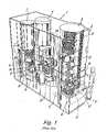
- FIGS. 1 and 2a wafer processing system according to the prior art is described.
- the subsequent figures and corresponding text belowillustrate how the preferred embodiment is adapted to this particular wafer processing system.
- the skilled artisanwill readily appreciate, however, that the principles and advantages of the I/O ports and storage positions described herein can be readily adapted to other processing systems where substrates are supplied to the system in holders such as cassettes.
- FIG. 1shows, diagrammatically and partially exposed, a perspective view and FIG. 2 shows a plan view of a wafer processing system for processing, e.g., 300-mm wafers supplied in 300-mm FOUP cassettes, according to the prior art.
- the wafer processing systemis indicated in its entirety by reference numeral 1 .
- This system 1comprises a housing 2 and is generally installed in a so-called “clean room.”
- partitions 3 , 4 and 5are also present.
- the housing 2delimits, with the partition 3 , a processing area or chamber 21 .
- the processing area 21comprises vertical furnaces 6 , 7 .
- the housing 2 and the partitions 3 and 4define a wafer handling chamber or station 22 .
- a cassette transfer chamber 23is defined within the housing 2 between partitions 4 and 5 .
- An input/output station 40 for transferring cassettes 10 into and out of the system 1is disposed adjacent to and in front of the cassette transfer chamber 23 .
- the input/output station 40can also be referred to as a front end, as it is located at a front, or entrance to, the processing system 1 .
- the input/output station 40includes two input/output ports 41 , each port comprising a platform to support a cassette and a closeable opening 42 which allow cassettes 10 access into the interior of the housing 2 .
- the cassettescan be, e.g., a 300-mm FOUP cassette, for holding 300-mm substrates, or a 200-mm open cassette, for holding 200-mm substrates.
- the system 1is preferably provided with a tool set which allows it to interface with either 300-mm FOUP cassettes or 200-mm open cassettes.
- a tool setis described in U.S. Pat. No. 6,632,068, the entire disclosure of which is incorporated herein by reference.
- Wafers 13are supplied in cassettes 10 , which are placed on the input/output station, or system front-end, 40 from the clean room side.
- the cassettesare placed coplanar, the side from which the wafers can be removed being substantially parallel with the partition 5 and facing the closeable openings 42 .
- the cassettesare rotated so that the side from which the wafers can be removed is oriented perpendicular to a radial extension direction of the cassette handling device 31 .
- FIGS. 1 and 2the cassette on the right input/output position is shown in such a rotated orientation and the cassette on the left input/output position is shown in a coplanar orientation.
- the cassette handling device 31 within the cassette transfer chamber 23grips and transfers the cassettes 10 from the input/output station 40 through the closable opening 42 into a cassette store 8 located in the cassette transfer chamber 23 .
- the cassette store 8is provided with a number of rotary platforms 27 above one another, on which the cassettes 10 are stored.
- the cassette handling device 31is movable in a vertical direction by means of an elevator 35 so that the different platforms 27 can be reached.
- the cassette handling device 31is provided with a cassette end effector 32 , which has dimensions a little smaller than those of a series of cut-outs 26 in the rotary platforms 27 .
- the end effector 32can be lowered through one of the cut-outs 26 in one of the platforms 27 to place the cassette 10 on the platform 27 . Subsequently, the cassette handler 31 can be retracted from cassette store 8 .
- the cassette handling device 31is mounted such that it is able to transfer cassettes between the input/output station 40 and the store 8 .
- the device 31is also capable of transferring cassettes between the store 8 and a rotatable cassette transfer platform 30 , or between the input/output station 40 and the rotatable cassette transfer platform 30 .
- the rotatable cassette transfer platform 30is constructed such that, on rotation, the cassette 10 is placed against the partition 4 between the cassette transfer chamber 23 and the wafer handling chamber 22 .
- the partition 4is provided with an openable closure and a closure mechanism, together forming an interface schematically indicated by reference numeral 37 .
- the interface 37is preferably configured for 300-mm FOUP cassettes. After placing the cassette 10 against the interface 37 in the partition 4 , the closure mechanism grips and unlocks the closure of the FOUP cassette 10 and simultaneously opens the closure in the partition 4 and the closure of the FOUP cassette 10 , thereby allowing a wafer handling device 24 within the wafer handling chamber 22 to access substrates in the FOUP cassette 10 .
- the wafer handling device 24transfers wafers between a cassette 10 and a wafer boat 12 .
- a boat transfer arm 16moves the wafer boat 12 through a closable opening in partition 3 from the wafer handling chamber 22 into the processing chamber 21 .
- the processing chamber 21is provided with a rotary boat transfer platform 11 , supporting the wafer boat 12 .
- Two reactors, which in this case comprise furnaces 6 , 7are arranged in the processing chamber 21 .
- the furnaces 6 , 7are positioned vertically and wafer boats, indicated by 12 , filled with wafers 13 , are introduced into the furnaces 6 , 7 in the vertical direction from below.
- each furnace 6 , 7has an insertion arm 14 , which is movable in the vertical direction. Only one insertion arm 14 is illustrated in FIG. 1 .
- the treatment of a large number of waferscan be carried out as follows:
- the operatorshown diagrammatically in FIG. 1 , loads the store 8 by introducing a number of cassettes 10 on the input/output station 40 and carrying out control operations on a control panel 36 .
- the illustrated input/output station 40has two input/output ports 41 , each input/output port provided with a closeable opening 42 , through which a cassette 10 can be received into the cassette transfer chamber 23 .
- Each of the cassettes 10is transferred from the input/output station 40 , through a closeable opening, with the aid of the cassette handling device 31 into the storage compartments 9 made for these cassettes 10 in the store 8 , specifically on the stacked rotary platforms 27 .
- By rotation of the store 8 and use of the elevator 35it is possible to fill various compartments with the cassettes 10 . After filling the store 8 , no further human interaction is required with this automated installation.
- the cassettes 10 concernedare then removed from the store 8 by the cassette handling device 31 and placed on the cassette transfer platform 30 .
- the cassette transfer platform 30comprises two levels, schematically indicated in FIG. 1 , each level capable of receiving a FOUP cassette 10 , where the two levels can be rotated independently of one another.
- the cassettes 10are placed against partition 4 .
- the wafersare removed by the wafer handler 24 and placed in a wafer boat 12 .
- the closure 19 in partition 3is opened and the wafer boat 12 is placed on the rotary boat transfer platform 11 by the boat transfer arm 16 .
- the boat transfer platform 11then moves the wafer boat 12 within the process chamber 21 to a position below the reactor to be loaded.
- the insertion mechanism or elevator 14moves the boat into the reactor 6 or 7 .
- Treated wafersexecute a movement which is the reverse of the movement described above.
- FIGS. 3-5Eshow a system 100 according preferred embodiments, which have features of FIGS. 1 and 2 . Illustrated features corresponding to those of the previously described system are referenced by similar reference numerals.
- FIGS. 3 , 4 and 5illustrate schematic side, top plan and front views, respectively, of the system 100 .
- the system 100is provided within a clean room 101 .
- the system 100has a front-end 102 for receiving and storing cassettes 10 , which can be, e.g., 300-mm FOUP cassettes and/or 200-mm cassettes.
- the front-end 102is provided with input/output ports 41 a , 41 b which allow cassettes 10 access into the housing 103 across the front-end partition 104 .
- Partitions 104 and 4along with the housing 103 , define the cassette transfer chamber 23 .
- Farther away from the front-end 102 , partitions 4 and 3 , along with the housing 103define the wafer handling chamber or station 22 .
- the partition 3with the housing 103 , then delimits the processing area or chamber 21 .
- the processing area 21comprises two vertical furnaces 6 , 7 ( FIG. 4 ).
- the front-end 102includes one or more lower input/output ports 41 a , and one or more upper input/output ports 41 b , the lower and upper input/output ports 41 a , 41 b disposed on two different vertical levels.
- at least one storage position 43is provided. In the illustrated embodiment, two vertical levels of storage positions 43 are provided. The storage positions 43 are preferably disposed on a vertical level between upper input/output port 41 b and lower input/output port 41 a .
- the lower input/output port 41 ais preferably positioned at a height specified by SEMI standards (SEMI E15.1, incorporated herein by reference) and the upper input/output port 41 b is preferably positioned at the maximum height allowed under SEMI E15.1, thereby advantageously accommodating the two vertical levels of storage positions 43 while still maintaining compatibility with other equipment in existing processing system installations, particularly standard overhead hoist vehicle (OHV) systems.
- SEMI E15.1SEMI E15.1
- OOVoverhead hoist vehicle
- the bottom of the lower input/output port 41 ais 900 mm ⁇ about 10 mm above the clean room floor, and the upper input/output port 41 b is positioned so that the top of a cassette at the upper input/output port 41 b is about 2600 mm above the clean room floor.
- the input/output ports 41 a , 41 bcan be coplanar, to receive a cassette from the clean room side such that the cassette side from which the wafers can be removed is disposed parallel to partition 102 and to openable closures 42 in partition 104 .
- the cassetteis rotated so that the cassette side from which the wafers can be removed is oriented perpendicular to a radial extension direction of the cassette handling device 31 to facilitate gripping by cassette handling device 31 .
- This rotationcan be performed by a rotatable platform supporting the cassettes at the input/output ports 41 a , 41 b .
- the rotationcan be performed by providing the end effector 32 of the cassette handling device 31 with a rotatable connection to the extendable arm and rotating the end effector.
- the storage positions 43are shown in a coplanar orientation relative to partition 102 for ease of illustration.
- the storage positions 43are oriented slightly rotated in a horizontal plane relative to the orientation illustrated in FIG. 3 so that the side from which the wafers can be removed is oriented perpendicular to a radial extension direction of the cassette handling device 31 (see FIG. 5B ).
- the storage positions 43are fixed, and not provided with a rotation mechanism.
- the input/output ports 41 a , 41 b and the storage positions 43have fixed vertical positions relative to one another, such that cassettes 10 held at the input/output ports 41 a , 41 b and the storage positions 43 are also in a fixed vertical position relative to one another.
- the input/output ports 41 a , 41 b and the storage positions 43can include platforms, as shown, or other devices for mechanically supporting the cassettes 10 .
- FIG. 5Ais a top plan view of the front end 102 showing upper input/output positions 41 b
- FIG. 5Bis a section along B-B and showing storage positions 43
- FIG. 5Cis a section along C-C showing lower input/output positions 41 a
- FIG. 5Dis a side view and indicates the levels of the cross-sections B-B and C-C.
- the cassettesare placed by an operator, AGV or OHS in a coplanar orientation and can be rotated by a rotatable platform.
- FIG. 5Eis a schematic front view. The cassettes on the storage positions 43 and the cassette on the lower left input/output position 41 a are shown in a rotated orientation.
- the front-end 102can include two columns of input/output ports 41 a , 41 b and the storage positions 43 . It will be appreciated that on some vertical levels both input/output ports and storage positions can be provided. In addition, it will be appreciated that each of the input/output ports 41 a , 41 b can also function as storage positions, as cassettes 10 can also be temporarily stored at those ports 41 a , 41 b.
- one single lower input/output port 41 acan be provided, along with a storage position at the same vertical level.
- two upper input/output ports 41 bcan be provided, with two pairs of storage positions 43 provided at two vertical levels between the upper input/output ports 41 b and the lower input/output port 41 a .
- the upper input/output ports 41 bcan be utilized for loading of cassettes 10 into the housing 103 during normal operation of the processing system 100
- the lower input/output port 41 ais advantageously at a height accessible to human operators and can be used as input/output station during maintenance operations and as storage position during normal processing.
- an additional storage position 43is preferably provided at the same vertical level as the lower input/output port 41 a.
- storage positions 43are separated from the clean room by a housing 120 , and are preferably only accessed by cassette handling device 31 through an opening in partition 104 .
- Lower input/output ports 41 aare provided with closable openings 142 in partition 104 , which is closed during placement or removal of the cassette by the operator and opens to allow gripping of the cassette by cassette handler device 31 .
- Cassettes 10are transferred inside the housing 103 using a cassette handler 31 , which is preferably a computer-controlled robot.
- the cassette handler 31is disposed inside the housing 103 and moves the cassettes 10 inward, relative to the exterior of the housing.
- the cassette handler 31is preferably a random access handler which can access cassettes 10 at any of the input/output ports 41 a , 41 b . It will be appreciated that cassettes 10 at pure storage positions 43 may need to be moved to an open input/output port 41 a , 41 b to allow transfer of those cassettes 10 out of the housing 103 . Movement of cassettes outside of the housing 103 can be performed, e.g., using a robot (not shown) external to the housing 103 , or by a human operator.
- the cassette transfer region 23houses a cassette transfer mechanism.
- the cassette transfer mechanismincludes the cassette handler 31 and the cassette transfer platform 30 .
- the cassette handler 31includes an elevator 35 which allows access to the multiple rotary platforms 27 of the cassette store 8 , and serves to transfer cassettes among the input/output ports 41 a , 41 b , the cassette store 8 and the cassette transfer platform 30 .
- the cassette transfer platform 30places cassettes into active communication with the interface 37 between the cassette transfer chamber 23 and the wafer handling chamber 22 , through which the wafer handling robot 24 can remove or replace substrates, such as semiconductor wafers.
- the cassette transfer platform 30can include two independently operable levels for independently moving two cassettes 10 to interface with two openings in the interface 37 ( FIG. 3 ). It will be appreciated that the wafer handling robot 24 can move substrates between the cassettes 10 and wafer boats for holding the substrates during processing in furnaces 6 , 7 ( FIG. 4 ). In the illustrated embodiment, the cassette handler 31 transfers cassettes 10 onto store 8 with the side from which the wafers can be removed facing out, thus facilitating efficient storage on the round store 8 with narrow cassette ends facing the center of the rotary platforms 27 . Similarly, cassette handler 31 transfers cassettes 10 onto transfer platform 30 with the side from which the wafers can be removed facing the cassette handler elevator 35 . The cassette transfer platform 30 is therefore configured to turn cassettes received from the cassette handler 31 until the side from which the wafers can be removed faces the interface 37 .
- Movements within the cassette transfer regionare controlled by a cassette handling controller, including a central processing unit (CPU) and program therefor.
- the cassette handling controllerinstructs all movement of the cassette handler 31 , rotation of the rotary platforms within the cassette store 8 , rotation of the cassette transfer platform 30 and rotation of cassettes 10 at the input/output station 40 .
- Sensorsare also connected to this controller to monitor the status of the cassette transfer process.
- At least one additional interior storage position 44can be provided in the cassette transfer region 23 in some preferred embodiments.
- the interior storage positions 44are disposed above, and particularly directly above, the cassette transfer platform 30 .
- the interior storage positions 44are disposed directly above the position occupied by a cassette after first loading the cassette onto the platform 30 using the cassette handler 31 ( FIG. 4 ).
- the interior storage positions 44are also accessible by the cassette handler 31 , which can be used to transfer cassettes to and from those positions 44 .
- the interior storage positions 44can include platforms, such as shelves, or other devices for supporting the cassettes 10 . In some embodiments, up to four interior storage positions 44 can be provided above the cassette transfer platform 30 .
- the interior storage positions 44can be used to store some cassettes 10 in lieu of storage in the cassette store 8 , or the interior storage positions 44 can be used as an intermediary storage position for cassettes 10 being transferred between the cassette store 8 and the cassette transfer platform 30 .
- the interior storage positions 44can be accessed by the same cassette handler 31 used to access cassettes 10 at the input/output ports 41 a , 41 b.
- the storage positions 44allow efficient use of the interior volume of the housing by providing additional cassette storage capabilities in an otherwise empty volume. Moreover, the proximity of the storage positions 44 to the cassette transfer platform 30 can decrease the transfer time of cassettes 10 to the cassette transfer platform, thereby increasing the overall rate at which substrates can be loaded onto a wafer boat for processing in furnaces 6 , 7 . In some other embodiments, one or more of the storage positions can be employed as a position for a metrology tool (not shown), accessible from wafer handling chamber 22 .
Landscapes
- Engineering & Computer Science (AREA)
- Physics & Mathematics (AREA)
- Condensed Matter Physics & Semiconductors (AREA)
- General Physics & Mathematics (AREA)
- Manufacturing & Machinery (AREA)
- Computer Hardware Design (AREA)
- Microelectronics & Electronic Packaging (AREA)
- Power Engineering (AREA)
- Container, Conveyance, Adherence, Positioning, Of Wafer (AREA)
Abstract
Description
- The invention relates to semiconductor substrate processing and, more particularly, to storage of substrate carriers in a processing system.
- Semiconductor fabrication systems are under constant pressure to increase throughput. This pressure is due to many factors, including the expense associated with operating semiconductor fabrication equipment and the desire to maximize the yield of substrates processed in the equipment.
- A semiconductor fabrication system can include various stations and pieces of equipment housed in a clean room. For example, such a system can include reactors, robots for handling semiconductor substrates and cassettes which hold the substrates, input/output ports in system front-ends for bringing substrates into and sending substrates out of the system, storage units, metrology tools, etc. Each station or piece of equipment has the potential to cause a bottleneck to the flow of substrates through the system, thereby degrading the throughput of the system as a whole.
- Accordingly, a need exists for apparatus and methods that minimize bottle-necks in a semiconductor fabrication system.
- According to one aspect of the invention, a semiconductor substrate processing system is provided. The system comprises a housing for separating the system from a surrounding clean room. A reactor is provided within the housing and a front-end for loading substrate cassettes into the housing. The front end is disposed adjacent to and in front of the housing. The front-end comprises at least one lower input/output port allowing cassettes access from the clean room into the housing; at least one upper input/output port disposed above the at least one lower input/output port and allowing cassettes access from the clean room into the housing; and at least one cassette storage position disposed at a vertical level between the at least one lower input/output port and the at least one upper input/output port. The storage position is configured to receive cassettes transported out of the housing and configured to allow cassette transport into the housing.
- According to another aspect of the invention, a loading station for a batch semiconductor fabrication system is provided. The loading station comprises a lower input/output port for holding a substrate cassette and which is configured to allow cassette access into a housing of the semiconductor fabrication system. The loading station also includes an upper input/output port for holding a substrate cassette. The upper input/output port is disposed above the lower input/output port and is configured to allow cassette access into the housing. The loading station also includes at least one storage position for holding a substrate cassette. The at least one storage position is disposed vertically between the lower input/output port and the upper input/output port.
- According to yet another aspect of the invention, a method for semiconductor fabrication is provided. The method comprises providing a semiconductor fabrication system having a loading station for loading cassettes into a housing of the system. A first cassette is held at a first vertical level at the loading station. A second cassette is held at a second vertical level at the loading station. The method also includes holding a third cassette at a third vertical level at the loading station.
- The invention will be better understood from the Detailed Description of the Preferred Embodiments and from the appended drawings, which are meant to illustrate and not to limit the invention, and wherein:
FIG. 1 is a perspective view of a semiconductor fabrication system, constructed in accordance with the prior art;FIG. 2 is a schematic top plan view of the system ofFIG. 1 ;FIG. 3 is a schematic side view of a system in accordance with preferred embodiments of the invention;FIG. 4 is a schematic top plan view of the system ofFIG. 3 , in accordance with preferred embodiments of the invention; andFIGS. 5A-5E are further schematic top plan, side and front views of a system in accordance with preferred embodiments of the invention.- Typically, substrates to be processed in semiconductor processing or fabrication systems are delivered to the systems in cassettes. The cassettes can be loaded into the housing of the processing system via the front-end of the system, which can include two input/output ports in some systems. Once inside the housing, substrates, such as semiconductor wafers, can be taken out of the cassettes and loaded into a reactor for processing in the reactor. Thus, the supply of substrates to the reactors depends partly upon the supply of cassettes to the system front-end.
- It has been found that processing systems that process substrates quickly, such as dual reactor systems, can process substrates more quickly than unprocessed substrates can be delivered to and supplied through access ports of the front-end. As a result, the reactors can remain idle while unprocessed substrates are provided to the reactors. Thus, the ability to supply cassettes with unprocessed substrates to the processing system can be a bottleneck which decreases the throughput of the system. Semiconductor fabrication systems containing two reactors within a common housing are disclosed in U.S. Pat. Nos. 6,607,602 and 6,632,068. The entire disclosures of each of these patents are incorporated herein by reference.
- Preferred embodiments of the invention increase throughput and minimize bottlenecks caused by shortages of unprocessed substrates by increasing the number of cassettes available to a system. The front-end of the system is provided with input/output (I/O) ports on at least two different vertical levels. Storage positions for substrate carriers, such as cassettes, can be provided on another vertical level. Preferably, the storage positions are provided on a vertical in between the levels of those input/output ports. Preferably, two levels of storage positions, each level preferably having two storage positions, are provided. In addition, each level of input/output ports preferably comprises two positions, the second position either being an additional input/output port or a storage position. Thus, a total of eight positions accommodating a total of eight substrate carriers can be provided at the front-end. In some embodiments, each of the input/output ports and the storage positions can be accessed by the same substrate carrier handler within the system, thereby facilitating loading and unloading of carriers into and out of the system. Preferably, the top level of input/output ports is set at the maximum height allowed under SEMI standards.
- In addition, it will be appreciated that in processing systems in which cassettes are taken into the interior of the processing system, substrates will typically need to be unloaded from the cassettes for processing and then loaded back into the cassettes after processing. The time required to supply cassettes with unprocessed wafers to the substrate transfer station and to remove cassettes with processed wafers from the substrate transfer station, can create a bottleneck. In some embodiments, additional storage positions can be provided inside the processing system, adjacent a station for transferring substrates into or out of cassettes, to minimize the time required to transport cassettes to and from the substrate transfer station.
- Advantageously, the preferred embodiments allow for an increase in the number of cassettes immediately available at the front-end of a processing system, thereby removing a potential bottleneck at the front-end of the processing system. Also, by vertically distributing additional input/output ports and storage positions over existing input/output ports, the footprint of the processing system is unchanged, thereby preserving valuable floor space in a fabrication facility. Moreover, compliance with SEMI standards allows compatibility with other existing ancillary systems to be maintained. In addition, the additional storage positions inside the processing system can further increase the number of cassettes available to the processing system, thereby further reducing any bottlenecks.
- Reference will now be made to the Figures, in which like numerals refer to like parts throughout.
- With reference to
FIGS. 1 and 2 , a wafer processing system according to the prior art is described. The subsequent figures and corresponding text below illustrate how the preferred embodiment is adapted to this particular wafer processing system. The skilled artisan will readily appreciate, however, that the principles and advantages of the I/O ports and storage positions described herein can be readily adapted to other processing systems where substrates are supplied to the system in holders such as cassettes. FIG. 1 shows, diagrammatically and partially exposed, a perspective view andFIG. 2 shows a plan view of a wafer processing system for processing, e.g., 300-mm wafers supplied in 300-mm FOUP cassettes, according to the prior art. The wafer processing system is indicated in its entirety by reference numeral1. This system1 comprises a housing2 and is generally installed in a so-called “clean room.” In addition to the housing2,partitions partition 3, a processing area orchamber 21. In this example, theprocessing area 21 comprisesvertical furnaces partitions station 22. Acassette transfer chamber 23 is defined within the housing2 betweenpartitions 4 and5.- An input/
output station 40 for transferringcassettes 10 into and out of the system1, is disposed adjacent to and in front of thecassette transfer chamber 23. The input/output station 40 can also be referred to as a front end, as it is located at a front, or entrance to, the processing system1. The input/output station 40 includes two input/output ports 41, each port comprising a platform to support a cassette and acloseable opening 42 which allowcassettes 10 access into the interior of the housing2. The cassettes can be, e.g., a 300-mm FOUP cassette, for holding 300-mm substrates, or a 200-mm open cassette, for holding 200-mm substrates. The system1 is preferably provided with a tool set which allows it to interface with either 300-mm FOUP cassettes or 200-mm open cassettes. Such a tool set is described in U.S. Pat. No. 6,632,068, the entire disclosure of which is incorporated herein by reference. - Wafers13 are supplied in
cassettes 10, which are placed on the input/output station, or system front-end,40 from the clean room side. The cassettes are placed coplanar, the side from which the wafers can be removed being substantially parallel with the partition5 and facing thecloseable openings 42. Then the cassettes are rotated so that the side from which the wafers can be removed is oriented perpendicular to a radial extension direction of thecassette handling device 31. InFIGS. 1 and 2 the cassette on the right input/output position is shown in such a rotated orientation and the cassette on the left input/output position is shown in a coplanar orientation. Then thecassette handling device 31 within thecassette transfer chamber 23 grips and transfers thecassettes 10 from the input/output station 40 through theclosable opening 42 into acassette store 8 located in thecassette transfer chamber 23. Thecassette store 8 is provided with a number ofrotary platforms 27 above one another, on which thecassettes 10 are stored. Thecassette handling device 31 is movable in a vertical direction by means of anelevator 35 so that thedifferent platforms 27 can be reached. Thecassette handling device 31 is provided with acassette end effector 32, which has dimensions a little smaller than those of a series of cut-outs 26 in therotary platforms 27. After thecassette handling device 31 has transferred acassette 10 into thestore 8, theend effector 32 can be lowered through one of the cut-outs 26 in one of theplatforms 27 to place thecassette 10 on theplatform 27. Subsequently, thecassette handler 31 can be retracted fromcassette store 8. Thecassette handling device 31 is mounted such that it is able to transfer cassettes between the input/output station 40 and thestore 8. Thedevice 31 is also capable of transferring cassettes between thestore 8 and a rotatablecassette transfer platform 30, or between the input/output station 40 and the rotatablecassette transfer platform 30. - The rotatable
cassette transfer platform 30 is constructed such that, on rotation, thecassette 10 is placed against thepartition 4 between thecassette transfer chamber 23 and thewafer handling chamber 22. Thepartition 4 is provided with an openable closure and a closure mechanism, together forming an interface schematically indicated byreference numeral 37. Theinterface 37 is preferably configured for 300-mm FOUP cassettes. After placing thecassette 10 against theinterface 37 in thepartition 4, the closure mechanism grips and unlocks the closure of theFOUP cassette 10 and simultaneously opens the closure in thepartition 4 and the closure of theFOUP cassette 10, thereby allowing awafer handling device 24 within thewafer handling chamber 22 to access substrates in theFOUP cassette 10. - The
wafer handling device 24 transfers wafers between acassette 10 and a wafer boat12. After completion of the loading of wafers into the wafer boat12, aboat transfer arm 16 moves the wafer boat12 through a closable opening inpartition 3 from thewafer handling chamber 22 into theprocessing chamber 21. Theprocessing chamber 21 is provided with a rotaryboat transfer platform 11, supporting the wafer boat12. Two reactors, which in this case comprisefurnaces processing chamber 21. Thefurnaces furnaces furnace insertion arm 14, which is movable in the vertical direction. Only oneinsertion arm 14 is illustrated inFIG. 1 . - The treatment of a large number of wafers can be carried out as follows: The operator, shown diagrammatically in
FIG. 1 , loads thestore 8 by introducing a number ofcassettes 10 on the input/output station 40 and carrying out control operations on acontrol panel 36. The illustrated input/output station 40 has two input/output ports 41, each input/output port provided with acloseable opening 42, through which acassette 10 can be received into thecassette transfer chamber 23. Each of thecassettes 10 is transferred from the input/output station 40, through a closeable opening, with the aid of thecassette handling device 31 into thestorage compartments 9 made for thesecassettes 10 in thestore 8, specifically on thestacked rotary platforms 27. By rotation of thestore 8 and use of theelevator 35, it is possible to fill various compartments with thecassettes 10. After filling thestore 8, no further human interaction is required with this automated installation. - The
cassettes 10 concerned are then removed from thestore 8 by thecassette handling device 31 and placed on thecassette transfer platform 30. Thecassette transfer platform 30 comprises two levels, schematically indicated inFIG. 1 , each level capable of receiving aFOUP cassette 10, where the two levels can be rotated independently of one another. Upon rotation of thecassette transfer platform 30, thecassettes 10 are placed againstpartition 4. After opening of the closure of theFOUP cassette 10, together with theclosure 37 inpartition 4, the wafers are removed by thewafer handler 24 and placed in a wafer boat12. After the wafer boat12 has been filled, and becomes available for one of thereactors closure 19 inpartition 3 is opened and the wafer boat12 is placed on the rotaryboat transfer platform 11 by theboat transfer arm 16. Theboat transfer platform 11 then moves the wafer boat12 within theprocess chamber 21 to a position below the reactor to be loaded. Then the insertion mechanism orelevator 14 moves the boat into thereactor - This system is described in further detail in published PCT application WO 99/38199 and U.S. Pat. No. 6,663,332, the entire disclosures of which are incorporated herein by reference. Although an operator is described as introducing the
cassette 10 on the input/output station 40, the system is designed such that thecassettes 10 can alternatively be introduced on the input/output station by means of an automatic guided vehicle (AGV) or by an overhead hoist system, which are known in the art. In such cases, the control system of the wafer processing system can be connected to a host computer system that carries out the control functions. In such arrangements, no human interaction at the wafer processing system is required. FIGS. 3-5E show asystem 100 according preferred embodiments, which have features ofFIGS. 1 and 2 . Illustrated features corresponding to those of the previously described system are referenced by similar reference numerals.FIGS. 3 ,4 and5 illustrate schematic side, top plan and front views, respectively, of thesystem 100.- With reference to
FIGS. 3 and 4 , thesystem 100 is provided within aclean room 101. Thesystem 100 has a front-end 102 for receiving and storingcassettes 10, which can be, e.g., 300-mm FOUP cassettes and/or 200-mm cassettes. The front-end 102 is provided with input/output ports cassettes 10 access into thehousing 103 across the front-end partition 104.Partitions housing 103, define thecassette transfer chamber 23. Farther away from the front-end 102,partitions housing 103, define the wafer handling chamber orstation 22. Thepartition 3, with thehousing 103, then delimits the processing area orchamber 21. In the illustrated embodiment, theprocessing area 21 comprises twovertical furnaces 6,7 (FIG. 4 ). - The front-
end 102 includes one or more lower input/output ports 41a, and one or more upper input/output ports 41b, the lower and upper input/output ports storage position 43 is provided. In the illustrated embodiment, two vertical levels ofstorage positions 43 are provided. The storage positions43 are preferably disposed on a vertical level between upper input/output port 41band lower input/output port 41a. The lower input/output port 41ais preferably positioned at a height specified by SEMI standards (SEMI E15.1, incorporated herein by reference) and the upper input/output port 41bis preferably positioned at the maximum height allowed under SEMI E15.1, thereby advantageously accommodating the two vertical levels ofstorage positions 43 while still maintaining compatibility with other equipment in existing processing system installations, particularly standard overhead hoist vehicle (OHV) systems. Preferably, in accordance with SEMI E15.1, the bottom of the lower input/output port 41ais 900 mm±about 10 mm above the clean room floor, and the upper input/output port 41bis positioned so that the top of a cassette at the upper input/output port 41bis about 2600 mm above the clean room floor. - As illustrated, the input/
output ports openable closures 42 inpartition 104. After receipt, the cassette is rotated so that the cassette side from which the wafers can be removed is oriented perpendicular to a radial extension direction of thecassette handling device 31 to facilitate gripping bycassette handling device 31. This rotation can be performed by a rotatable platform supporting the cassettes at the input/output ports end effector 32 of thecassette handling device 31 with a rotatable connection to the extendable arm and rotating the end effector. InFIG. 3 , the storage positions43 are shown in a coplanar orientation relative to partition102 for ease of illustration. Preferably, the storage positions43 are oriented slightly rotated in a horizontal plane relative to the orientation illustrated inFIG. 3 so that the side from which the wafers can be removed is oriented perpendicular to a radial extension direction of the cassette handling device31 (seeFIG. 5B ). Preferably, the storage positions43 are fixed, and not provided with a rotation mechanism. Preferably, the input/output ports cassettes 10 held at the input/output ports output ports cassettes 10. FIG. 5A is a top plan view of thefront end 102 showing upper input/output positions 41b,FIG. 5B is a section along B-B and showingstorage positions 43,FIG. 5C is a section along C-C showing lower input/output positions 41a.FIG. 5D is a side view and indicates the levels of the cross-sections B-B and C-C. On input/output positions cassette handling device 31. As the cassettes may be placed and removed on the storage positions by thecassette handling device 31, there is no need or advantage in rotating the cassettes in a coplanar orientation. Therefore, a rotatable platform on the storage positions43 or arotatable end effector 32 oncassette handling device 31 may be omitted.FIG. 5E is a schematic front view. The cassettes on the storage positions43 and the cassette on the lower left input/output position 41aare shown in a rotated orientation.- With continued reference to
FIG. 5E , the front-end 102 can include two columns of input/output ports output ports cassettes 10 can also be temporarily stored at thoseports - For example, in some preferred embodiments, one single lower input/
output port 41acan be provided, along with a storage position at the same vertical level. In the same preferred embodiments, two upper input/output ports 41bcan be provided, with two pairs ofstorage positions 43 provided at two vertical levels between the upper input/output ports 41band the lower input/output port 41a. During processing, the upper input/output ports 41bcan be utilized for loading ofcassettes 10 into thehousing 103 during normal operation of theprocessing system 100, while the lower input/output port 41ais advantageously at a height accessible to human operators and can be used as input/output station during maintenance operations and as storage position during normal processing. To minimize system complexity and associated costs, anadditional storage position 43, rather than a more complex second lower input/output port 41a, is preferably provided at the same vertical level as the lower input/output port 41a. - As operators need to be protected against interference with moving parts such as
cassette handling device 31, storage positions43 are separated from the clean room by ahousing 120, and are preferably only accessed bycassette handling device 31 through an opening inpartition 104. Lower input/output ports 41aare provided with closable openings142 inpartition 104, which is closed during placement or removal of the cassette by the operator and opens to allow gripping of the cassette bycassette handler device 31. Cassettes 10 are transferred inside thehousing 103 using acassette handler 31, which is preferably a computer-controlled robot. Thecassette handler 31 is disposed inside thehousing 103 and moves thecassettes 10 inward, relative to the exterior of the housing. Thecassette handler 31 is preferably a random access handler which can accesscassettes 10 at any of the input/output ports cassettes 10 atpure storage positions 43 may need to be moved to an open input/output port cassettes 10 out of thehousing 103. Movement of cassettes outside of thehousing 103 can be performed, e.g., using a robot (not shown) external to thehousing 103, or by a human operator.- Movement of a
cassette 10 inside thehousing 103 transfers thecassette 10 into thecassette transfer region 23. Thecassette transfer region 23 houses a cassette transfer mechanism. In the illustrated embodiment, the cassette transfer mechanism includes thecassette handler 31 and thecassette transfer platform 30. Thecassette handler 31 includes anelevator 35 which allows access to the multiplerotary platforms 27 of thecassette store 8, and serves to transfer cassettes among the input/output ports cassette store 8 and thecassette transfer platform 30. Thecassette transfer platform 30, in turn, places cassettes into active communication with theinterface 37 between thecassette transfer chamber 23 and thewafer handling chamber 22, through which thewafer handling robot 24 can remove or replace substrates, such as semiconductor wafers. Thecassette transfer platform 30 can include two independently operable levels for independently moving twocassettes 10 to interface with two openings in the interface37 (FIG. 3 ). It will be appreciated that thewafer handling robot 24 can move substrates between thecassettes 10 and wafer boats for holding the substrates during processing infurnaces 6,7 (FIG. 4 ). In the illustrated embodiment, thecassette handler 31transfers cassettes 10 ontostore 8 with the side from which the wafers can be removed facing out, thus facilitating efficient storage on theround store 8 with narrow cassette ends facing the center of therotary platforms 27. Similarly,cassette handler 31transfers cassettes 10 ontotransfer platform 30 with the side from which the wafers can be removed facing thecassette handler elevator 35. Thecassette transfer platform 30 is therefore configured to turn cassettes received from thecassette handler 31 until the side from which the wafers can be removed faces theinterface 37. - Movements within the cassette transfer region are controlled by a cassette handling controller, including a central processing unit (CPU) and program therefor. In particular, the cassette handling controller instructs all movement of the
cassette handler 31, rotation of the rotary platforms within thecassette store 8, rotation of thecassette transfer platform 30 and rotation ofcassettes 10 at the input/output station 40. Sensors are also connected to this controller to monitor the status of the cassette transfer process. - With continued reference to
FIGS. 3 and 4 , at least one additionalinterior storage position 44 can be provided in thecassette transfer region 23 in some preferred embodiments. Preferably, the interior storage positions44 are disposed above, and particularly directly above, thecassette transfer platform 30. In some embodiments, the interior storage positions44 are disposed directly above the position occupied by a cassette after first loading the cassette onto theplatform 30 using the cassette handler31 (FIG. 4 ). Advantageously, the interior storage positions44 are also accessible by thecassette handler 31, which can be used to transfer cassettes to and from thosepositions 44. The interior storage positions44 can include platforms, such as shelves, or other devices for supporting thecassettes 10. In some embodiments, up to four interior storage positions44 can be provided above thecassette transfer platform 30. It will be appreciated that the interior storage positions44 can be used to store somecassettes 10 in lieu of storage in thecassette store 8, or the interior storage positions44 can be used as an intermediary storage position forcassettes 10 being transferred between thecassette store 8 and thecassette transfer platform 30. Preferably, the interior storage positions44 can be accessed by thesame cassette handler 31 used to accesscassettes 10 at the input/output ports - Advantageously, the storage positions44 allow efficient use of the interior volume of the housing by providing additional cassette storage capabilities in an otherwise empty volume. Moreover, the proximity of the storage positions44 to the
cassette transfer platform 30 can decrease the transfer time ofcassettes 10 to the cassette transfer platform, thereby increasing the overall rate at which substrates can be loaded onto a wafer boat for processing infurnaces wafer handling chamber 22. - It will be appreciated by those skilled in the art that various omissions, additions and modifications may be made to the methods and apparatus described above without departing from the scope of the invention. All such modifications and changes are intended to fall within the scope of the invention, as defined by the appended claims.
Claims (36)
Priority Applications (2)
| Application Number | Priority Date | Filing Date | Title |
|---|---|---|---|
| US11/525,724US7740437B2 (en) | 2006-09-22 | 2006-09-22 | Processing system with increased cassette storage capacity |
| JP2007147988AJP2008078616A (en) | 2006-09-22 | 2007-06-04 | Treatment device increased in cassette storage capacity |
Applications Claiming Priority (1)
| Application Number | Priority Date | Filing Date | Title |
|---|---|---|---|
| US11/525,724US7740437B2 (en) | 2006-09-22 | 2006-09-22 | Processing system with increased cassette storage capacity |
Publications (2)
| Publication Number | Publication Date |
|---|---|
| US20080075562A1true US20080075562A1 (en) | 2008-03-27 |
| US7740437B2 US7740437B2 (en) | 2010-06-22 |
Family
ID=39225141
Family Applications (1)
| Application Number | Title | Priority Date | Filing Date |
|---|---|---|---|
| US11/525,724Active2028-10-24US7740437B2 (en) | 2006-09-22 | 2006-09-22 | Processing system with increased cassette storage capacity |
Country Status (2)
| Country | Link |
|---|---|
| US (1) | US7740437B2 (en) |
| JP (1) | JP2008078616A (en) |
Cited By (356)
| Publication number | Priority date | Publication date | Assignee | Title |
|---|---|---|---|---|
| US20130085593A1 (en)* | 2011-09-29 | 2013-04-04 | Theodorus G.M. Oosterlaken | Modular semiconductor processing system |
| WO2018178771A1 (en)* | 2017-03-31 | 2018-10-04 | Asm Ip Holding B.V. | Apparatus and method for manufacturing a semiconductor device |
| US10229833B2 (en) | 2016-11-01 | 2019-03-12 | Asm Ip Holding B.V. | Methods for forming a transition metal nitride film on a substrate by atomic layer deposition and related semiconductor device structures |
| US10249577B2 (en) | 2016-05-17 | 2019-04-02 | Asm Ip Holding B.V. | Method of forming metal interconnection and method of fabricating semiconductor apparatus using the method |
| US10249524B2 (en) | 2017-08-09 | 2019-04-02 | Asm Ip Holding B.V. | Cassette holder assembly for a substrate cassette and holding member for use in such assembly |
| US10262859B2 (en) | 2016-03-24 | 2019-04-16 | Asm Ip Holding B.V. | Process for forming a film on a substrate using multi-port injection assemblies |
| US10269558B2 (en) | 2016-12-22 | 2019-04-23 | Asm Ip Holding B.V. | Method of forming a structure on a substrate |
| US10276355B2 (en) | 2015-03-12 | 2019-04-30 | Asm Ip Holding B.V. | Multi-zone reactor, system including the reactor, and method of using the same |
| US10283353B2 (en) | 2017-03-29 | 2019-05-07 | Asm Ip Holding B.V. | Method of reforming insulating film deposited on substrate with recess pattern |
| US10290508B1 (en) | 2017-12-05 | 2019-05-14 | Asm Ip Holding B.V. | Method for forming vertical spacers for spacer-defined patterning |
| US10312129B2 (en) | 2015-09-29 | 2019-06-04 | Asm Ip Holding B.V. | Variable adjustment for precise matching of multiple chamber cavity housings |
| US10312055B2 (en) | 2017-07-26 | 2019-06-04 | Asm Ip Holding B.V. | Method of depositing film by PEALD using negative bias |
| US10319588B2 (en) | 2017-10-10 | 2019-06-11 | Asm Ip Holding B.V. | Method for depositing a metal chalcogenide on a substrate by cyclical deposition |
| US10322384B2 (en) | 2015-11-09 | 2019-06-18 | Asm Ip Holding B.V. | Counter flow mixer for process chamber |
| US10340135B2 (en) | 2016-11-28 | 2019-07-02 | Asm Ip Holding B.V. | Method of topologically restricted plasma-enhanced cyclic deposition of silicon or metal nitride |
| US10340125B2 (en) | 2013-03-08 | 2019-07-02 | Asm Ip Holding B.V. | Pulsed remote plasma method and system |
| US10343920B2 (en) | 2016-03-18 | 2019-07-09 | Asm Ip Holding B.V. | Aligned carbon nanotubes |
| US10361201B2 (en) | 2013-09-27 | 2019-07-23 | Asm Ip Holding B.V. | Semiconductor structure and device formed using selective epitaxial process |
| US10364496B2 (en) | 2011-06-27 | 2019-07-30 | Asm Ip Holding B.V. | Dual section module having shared and unshared mass flow controllers |
| US10367080B2 (en) | 2016-05-02 | 2019-07-30 | Asm Ip Holding B.V. | Method of forming a germanium oxynitride film |
| US10364493B2 (en) | 2016-08-25 | 2019-07-30 | Asm Ip Holding B.V. | Exhaust apparatus and substrate processing apparatus having an exhaust line with a first ring having at least one hole on a lateral side thereof placed in the exhaust line |
| US10366864B2 (en) | 2013-03-08 | 2019-07-30 | Asm Ip Holding B.V. | Method and system for in-situ formation of intermediate reactive species |
| US10378106B2 (en) | 2008-11-14 | 2019-08-13 | Asm Ip Holding B.V. | Method of forming insulation film by modified PEALD |
| US10381219B1 (en) | 2018-10-25 | 2019-08-13 | Asm Ip Holding B.V. | Methods for forming a silicon nitride film |
| US10381226B2 (en) | 2016-07-27 | 2019-08-13 | Asm Ip Holding B.V. | Method of processing substrate |
| US10388513B1 (en) | 2018-07-03 | 2019-08-20 | Asm Ip Holding B.V. | Method for depositing silicon-free carbon-containing film as gap-fill layer by pulse plasma-assisted deposition |
| US10388509B2 (en) | 2016-06-28 | 2019-08-20 | Asm Ip Holding B.V. | Formation of epitaxial layers via dislocation filtering |
| US10395919B2 (en) | 2016-07-28 | 2019-08-27 | Asm Ip Holding B.V. | Method and apparatus for filling a gap |
| US10403504B2 (en) | 2017-10-05 | 2019-09-03 | Asm Ip Holding B.V. | Method for selectively depositing a metallic film on a substrate |
| US10410943B2 (en) | 2016-10-13 | 2019-09-10 | Asm Ip Holding B.V. | Method for passivating a surface of a semiconductor and related systems |
| US10438965B2 (en) | 2014-12-22 | 2019-10-08 | Asm Ip Holding B.V. | Semiconductor device and manufacturing method thereof |
| US10435790B2 (en) | 2016-11-01 | 2019-10-08 | Asm Ip Holding B.V. | Method of subatmospheric plasma-enhanced ALD using capacitively coupled electrodes with narrow gap |
| US10446393B2 (en) | 2017-05-08 | 2019-10-15 | Asm Ip Holding B.V. | Methods for forming silicon-containing epitaxial layers and related semiconductor device structures |
| US10458018B2 (en) | 2015-06-26 | 2019-10-29 | Asm Ip Holding B.V. | Structures including metal carbide material, devices including the structures, and methods of forming same |
| US10468251B2 (en) | 2016-02-19 | 2019-11-05 | Asm Ip Holding B.V. | Method for forming spacers using silicon nitride film for spacer-defined multiple patterning |
| US10468262B2 (en) | 2017-02-15 | 2019-11-05 | Asm Ip Holding B.V. | Methods for forming a metallic film on a substrate by a cyclical deposition and related semiconductor device structures |
| US10480072B2 (en) | 2009-04-06 | 2019-11-19 | Asm Ip Holding B.V. | Semiconductor processing reactor and components thereof |
| US10483099B1 (en) | 2018-07-26 | 2019-11-19 | Asm Ip Holding B.V. | Method for forming thermally stable organosilicon polymer film |
| US10504742B2 (en) | 2017-05-31 | 2019-12-10 | Asm Ip Holding B.V. | Method of atomic layer etching using hydrogen plasma |
| US10501866B2 (en) | 2016-03-09 | 2019-12-10 | Asm Ip Holding B.V. | Gas distribution apparatus for improved film uniformity in an epitaxial system |
| US10510536B2 (en) | 2018-03-29 | 2019-12-17 | Asm Ip Holding B.V. | Method of depositing a co-doped polysilicon film on a surface of a substrate within a reaction chamber |
| US10529563B2 (en) | 2017-03-29 | 2020-01-07 | Asm Ip Holdings B.V. | Method for forming doped metal oxide films on a substrate by cyclical deposition and related semiconductor device structures |
| US10529542B2 (en) | 2015-03-11 | 2020-01-07 | Asm Ip Holdings B.V. | Cross-flow reactor and method |
| US10529554B2 (en) | 2016-02-19 | 2020-01-07 | Asm Ip Holding B.V. | Method for forming silicon nitride film selectively on sidewalls or flat surfaces of trenches |
| US10535516B2 (en) | 2018-02-01 | 2020-01-14 | Asm Ip Holdings B.V. | Method for depositing a semiconductor structure on a surface of a substrate and related semiconductor structures |
| US10541173B2 (en) | 2016-07-08 | 2020-01-21 | Asm Ip Holding B.V. | Selective deposition method to form air gaps |
| US10541333B2 (en) | 2017-07-19 | 2020-01-21 | Asm Ip Holding B.V. | Method for depositing a group IV semiconductor and related semiconductor device structures |
| US10559458B1 (en) | 2018-11-26 | 2020-02-11 | Asm Ip Holding B.V. | Method of forming oxynitride film |
| US10566223B2 (en) | 2012-08-28 | 2020-02-18 | Asm Ip Holdings B.V. | Systems and methods for dynamic semiconductor process scheduling |
| US10561975B2 (en) | 2014-10-07 | 2020-02-18 | Asm Ip Holdings B.V. | Variable conductance gas distribution apparatus and method |
| US10590535B2 (en) | 2017-07-26 | 2020-03-17 | Asm Ip Holdings B.V. | Chemical treatment, deposition and/or infiltration apparatus and method for using the same |
| US10600673B2 (en) | 2015-07-07 | 2020-03-24 | Asm Ip Holding B.V. | Magnetic susceptor to baseplate seal |
| US10607895B2 (en) | 2017-09-18 | 2020-03-31 | Asm Ip Holdings B.V. | Method for forming a semiconductor device structure comprising a gate fill metal |
| US10604847B2 (en) | 2014-03-18 | 2020-03-31 | Asm Ip Holding B.V. | Gas distribution system, reactor including the system, and methods of using the same |
| US10605530B2 (en) | 2017-07-26 | 2020-03-31 | Asm Ip Holding B.V. | Assembly of a liner and a flange for a vertical furnace as well as the liner and the vertical furnace |
| USD880437S1 (en) | 2018-02-01 | 2020-04-07 | Asm Ip Holding B.V. | Gas supply plate for semiconductor manufacturing apparatus |
| US10612137B2 (en) | 2016-07-08 | 2020-04-07 | Asm Ip Holdings B.V. | Organic reactants for atomic layer deposition |
| US10612136B2 (en) | 2018-06-29 | 2020-04-07 | ASM IP Holding, B.V. | Temperature-controlled flange and reactor system including same |
| US10622375B2 (en) | 2016-11-07 | 2020-04-14 | Asm Ip Holding B.V. | Method of processing a substrate and a device manufactured by using the method |
| US10643826B2 (en) | 2016-10-26 | 2020-05-05 | Asm Ip Holdings B.V. | Methods for thermally calibrating reaction chambers |
| US10643904B2 (en) | 2016-11-01 | 2020-05-05 | Asm Ip Holdings B.V. | Methods for forming a semiconductor device and related semiconductor device structures |
| US10658205B2 (en) | 2017-09-28 | 2020-05-19 | Asm Ip Holdings B.V. | Chemical dispensing apparatus and methods for dispensing a chemical to a reaction chamber |
| US10655221B2 (en) | 2017-02-09 | 2020-05-19 | Asm Ip Holding B.V. | Method for depositing oxide film by thermal ALD and PEALD |
| US10658181B2 (en) | 2018-02-20 | 2020-05-19 | Asm Ip Holding B.V. | Method of spacer-defined direct patterning in semiconductor fabrication |
| US10665452B2 (en) | 2016-05-02 | 2020-05-26 | Asm Ip Holdings B.V. | Source/drain performance through conformal solid state doping |
| US10683571B2 (en) | 2014-02-25 | 2020-06-16 | Asm Ip Holding B.V. | Gas supply manifold and method of supplying gases to chamber using same |
| US10685834B2 (en) | 2017-07-05 | 2020-06-16 | Asm Ip Holdings B.V. | Methods for forming a silicon germanium tin layer and related semiconductor device structures |
| US10692741B2 (en) | 2017-08-08 | 2020-06-23 | Asm Ip Holdings B.V. | Radiation shield |
| US10707106B2 (en) | 2011-06-06 | 2020-07-07 | Asm Ip Holding B.V. | High-throughput semiconductor-processing apparatus equipped with multiple dual-chamber modules |
| US10714350B2 (en) | 2016-11-01 | 2020-07-14 | ASM IP Holdings, B.V. | Methods for forming a transition metal niobium nitride film on a substrate by atomic layer deposition and related semiconductor device structures |
| US10714335B2 (en) | 2017-04-25 | 2020-07-14 | Asm Ip Holding B.V. | Method of depositing thin film and method of manufacturing semiconductor device |
| US10714315B2 (en) | 2012-10-12 | 2020-07-14 | Asm Ip Holdings B.V. | Semiconductor reaction chamber showerhead |
| US10714385B2 (en) | 2016-07-19 | 2020-07-14 | Asm Ip Holding B.V. | Selective deposition of tungsten |
| US10734244B2 (en) | 2017-11-16 | 2020-08-04 | Asm Ip Holding B.V. | Method of processing a substrate and a device manufactured by the same |
| US10734497B2 (en) | 2017-07-18 | 2020-08-04 | Asm Ip Holding B.V. | Methods for forming a semiconductor device structure and related semiconductor device structures |
| US10731249B2 (en) | 2018-02-15 | 2020-08-04 | Asm Ip Holding B.V. | Method of forming a transition metal containing film on a substrate by a cyclical deposition process, a method for supplying a transition metal halide compound to a reaction chamber, and related vapor deposition apparatus |
| US10741385B2 (en) | 2016-07-28 | 2020-08-11 | Asm Ip Holding B.V. | Method and apparatus for filling a gap |
| US10755922B2 (en) | 2018-07-03 | 2020-08-25 | Asm Ip Holding B.V. | Method for depositing silicon-free carbon-containing film as gap-fill layer by pulse plasma-assisted deposition |
| US10767789B2 (en) | 2018-07-16 | 2020-09-08 | Asm Ip Holding B.V. | Diaphragm valves, valve components, and methods for forming valve components |
| US10770286B2 (en) | 2017-05-08 | 2020-09-08 | Asm Ip Holdings B.V. | Methods for selectively forming a silicon nitride film on a substrate and related semiconductor device structures |
| US10770336B2 (en) | 2017-08-08 | 2020-09-08 | Asm Ip Holding B.V. | Substrate lift mechanism and reactor including same |
| US10787741B2 (en) | 2014-08-21 | 2020-09-29 | Asm Ip Holding B.V. | Method and system for in situ formation of gas-phase compounds |
| US10797133B2 (en) | 2018-06-21 | 2020-10-06 | Asm Ip Holding B.V. | Method for depositing a phosphorus doped silicon arsenide film and related semiconductor device structures |
| US10804098B2 (en) | 2009-08-14 | 2020-10-13 | Asm Ip Holding B.V. | Systems and methods for thin-film deposition of metal oxides using excited nitrogen-oxygen species |
| US10811256B2 (en) | 2018-10-16 | 2020-10-20 | Asm Ip Holding B.V. | Method for etching a carbon-containing feature |
| US10818758B2 (en) | 2018-11-16 | 2020-10-27 | Asm Ip Holding B.V. | Methods for forming a metal silicate film on a substrate in a reaction chamber and related semiconductor device structures |
| USD900036S1 (en) | 2017-08-24 | 2020-10-27 | Asm Ip Holding B.V. | Heater electrical connector and adapter |
| US10829852B2 (en) | 2018-08-16 | 2020-11-10 | Asm Ip Holding B.V. | Gas distribution device for a wafer processing apparatus |
| US10832903B2 (en) | 2011-10-28 | 2020-11-10 | Asm Ip Holding B.V. | Process feed management for semiconductor substrate processing |
| CN111952228A (en)* | 2019-05-16 | 2020-11-17 | Asm Ip控股有限公司 | Wafer boat handling device, vertical batch furnace and method |
| US10847365B2 (en) | 2018-10-11 | 2020-11-24 | Asm Ip Holding B.V. | Method of forming conformal silicon carbide film by cyclic CVD |
| US10847371B2 (en) | 2018-03-27 | 2020-11-24 | Asm Ip Holding B.V. | Method of forming an electrode on a substrate and a semiconductor device structure including an electrode |
| US10844484B2 (en) | 2017-09-22 | 2020-11-24 | Asm Ip Holding B.V. | Apparatus for dispensing a vapor phase reactant to a reaction chamber and related methods |
| US10847366B2 (en) | 2018-11-16 | 2020-11-24 | Asm Ip Holding B.V. | Methods for depositing a transition metal chalcogenide film on a substrate by a cyclical deposition process |
| US10851456B2 (en) | 2016-04-21 | 2020-12-01 | Asm Ip Holding B.V. | Deposition of metal borides |
| US10854498B2 (en) | 2011-07-15 | 2020-12-01 | Asm Ip Holding B.V. | Wafer-supporting device and method for producing same |
| USD903477S1 (en) | 2018-01-24 | 2020-12-01 | Asm Ip Holdings B.V. | Metal clamp |
| US10858737B2 (en) | 2014-07-28 | 2020-12-08 | Asm Ip Holding B.V. | Showerhead assembly and components thereof |
| US10867786B2 (en) | 2018-03-30 | 2020-12-15 | Asm Ip Holding B.V. | Substrate processing method |
| US10867788B2 (en) | 2016-12-28 | 2020-12-15 | Asm Ip Holding B.V. | Method of forming a structure on a substrate |
| US10865475B2 (en) | 2016-04-21 | 2020-12-15 | Asm Ip Holding B.V. | Deposition of metal borides and silicides |
| US10872771B2 (en) | 2018-01-16 | 2020-12-22 | Asm Ip Holding B. V. | Method for depositing a material film on a substrate within a reaction chamber by a cyclical deposition process and related device structures |
| US10883175B2 (en) | 2018-08-09 | 2021-01-05 | Asm Ip Holding B.V. | Vertical furnace for processing substrates and a liner for use therein |
| US10886123B2 (en) | 2017-06-02 | 2021-01-05 | Asm Ip Holding B.V. | Methods for forming low temperature semiconductor layers and related semiconductor device structures |
| US10892156B2 (en) | 2017-05-08 | 2021-01-12 | Asm Ip Holding B.V. | Methods for forming a silicon nitride film on a substrate and related semiconductor device structures |
| US10896820B2 (en) | 2018-02-14 | 2021-01-19 | Asm Ip Holding B.V. | Method for depositing a ruthenium-containing film on a substrate by a cyclical deposition process |
| US10910262B2 (en) | 2017-11-16 | 2021-02-02 | Asm Ip Holding B.V. | Method of selectively depositing a capping layer structure on a semiconductor device structure |
| US10914004B2 (en) | 2018-06-29 | 2021-02-09 | Asm Ip Holding B.V. | Thin-film deposition method and manufacturing method of semiconductor device |
| US10923344B2 (en) | 2017-10-30 | 2021-02-16 | Asm Ip Holding B.V. | Methods for forming a semiconductor structure and related semiconductor structures |
| US10928731B2 (en) | 2017-09-21 | 2021-02-23 | Asm Ip Holding B.V. | Method of sequential infiltration synthesis treatment of infiltrateable material and structures and devices formed using same |
| US10934619B2 (en) | 2016-11-15 | 2021-03-02 | Asm Ip Holding B.V. | Gas supply unit and substrate processing apparatus including the gas supply unit |
| US10941490B2 (en) | 2014-10-07 | 2021-03-09 | Asm Ip Holding B.V. | Multiple temperature range susceptor, assembly, reactor and system including the susceptor, and methods of using the same |
| US10975470B2 (en) | 2018-02-23 | 2021-04-13 | Asm Ip Holding B.V. | Apparatus for detecting or monitoring for a chemical precursor in a high temperature environment |
| US11001925B2 (en) | 2016-12-19 | 2021-05-11 | Asm Ip Holding B.V. | Substrate processing apparatus |
| US11015245B2 (en) | 2014-03-19 | 2021-05-25 | Asm Ip Holding B.V. | Gas-phase reactor and system having exhaust plenum and components thereof |
| US11018047B2 (en) | 2018-01-25 | 2021-05-25 | Asm Ip Holding B.V. | Hybrid lift pin |
| US11018002B2 (en) | 2017-07-19 | 2021-05-25 | Asm Ip Holding B.V. | Method for selectively depositing a Group IV semiconductor and related semiconductor device structures |
| US11022879B2 (en) | 2017-11-24 | 2021-06-01 | Asm Ip Holding B.V. | Method of forming an enhanced unexposed photoresist layer |
| US11024523B2 (en) | 2018-09-11 | 2021-06-01 | Asm Ip Holding B.V. | Substrate processing apparatus and method |
| US11031242B2 (en) | 2018-11-07 | 2021-06-08 | Asm Ip Holding B.V. | Methods for depositing a boron doped silicon germanium film |
| USD922229S1 (en) | 2019-06-05 | 2021-06-15 | Asm Ip Holding B.V. | Device for controlling a temperature of a gas supply unit |
| US11049751B2 (en) | 2018-09-14 | 2021-06-29 | Asm Ip Holding B.V. | Cassette supply system to store and handle cassettes and processing apparatus equipped therewith |
| US11056344B2 (en) | 2017-08-30 | 2021-07-06 | Asm Ip Holding B.V. | Layer forming method |
| US11053591B2 (en) | 2018-08-06 | 2021-07-06 | Asm Ip Holding B.V. | Multi-port gas injection system and reactor system including same |
| US11056567B2 (en) | 2018-05-11 | 2021-07-06 | Asm Ip Holding B.V. | Method of forming a doped metal carbide film on a substrate and related semiconductor device structures |
| US11069510B2 (en) | 2017-08-30 | 2021-07-20 | Asm Ip Holding B.V. | Substrate processing apparatus |
| US11081345B2 (en) | 2018-02-06 | 2021-08-03 | Asm Ip Holding B.V. | Method of post-deposition treatment for silicon oxide film |
| US11088002B2 (en) | 2018-03-29 | 2021-08-10 | Asm Ip Holding B.V. | Substrate rack and a substrate processing system and method |
| US11087997B2 (en) | 2018-10-31 | 2021-08-10 | Asm Ip Holding B.V. | Substrate processing apparatus for processing substrates |
| US11114294B2 (en) | 2019-03-08 | 2021-09-07 | Asm Ip Holding B.V. | Structure including SiOC layer and method of forming same |
| US11114283B2 (en) | 2018-03-16 | 2021-09-07 | Asm Ip Holding B.V. | Reactor, system including the reactor, and methods of manufacturing and using same |
| USD930782S1 (en) | 2019-08-22 | 2021-09-14 | Asm Ip Holding B.V. | Gas distributor |
| US11127589B2 (en) | 2019-02-01 | 2021-09-21 | Asm Ip Holding B.V. | Method of topology-selective film formation of silicon oxide |
| US11127617B2 (en) | 2017-11-27 | 2021-09-21 | Asm Ip Holding B.V. | Storage device for storing wafer cassettes for use with a batch furnace |
| USD931978S1 (en) | 2019-06-27 | 2021-09-28 | Asm Ip Holding B.V. | Showerhead vacuum transport |
| US11139191B2 (en) | 2017-08-09 | 2021-10-05 | Asm Ip Holding B.V. | Storage apparatus for storing cassettes for substrates and processing apparatus equipped therewith |
| US11139308B2 (en) | 2015-12-29 | 2021-10-05 | Asm Ip Holding B.V. | Atomic layer deposition of III-V compounds to form V-NAND devices |
| US11158513B2 (en) | 2018-12-13 | 2021-10-26 | Asm Ip Holding B.V. | Methods for forming a rhenium-containing film on a substrate by a cyclical deposition process and related semiconductor device structures |
| US11171025B2 (en) | 2019-01-22 | 2021-11-09 | Asm Ip Holding B.V. | Substrate processing device |
| USD935572S1 (en) | 2019-05-24 | 2021-11-09 | Asm Ip Holding B.V. | Gas channel plate |
| US11205585B2 (en) | 2016-07-28 | 2021-12-21 | Asm Ip Holding B.V. | Substrate processing apparatus and method of operating the same |
| US11217444B2 (en) | 2018-11-30 | 2022-01-04 | Asm Ip Holding B.V. | Method for forming an ultraviolet radiation responsive metal oxide-containing film |
| USD940837S1 (en) | 2019-08-22 | 2022-01-11 | Asm Ip Holding B.V. | Electrode |
| US11222772B2 (en) | 2016-12-14 | 2022-01-11 | Asm Ip Holding B.V. | Substrate processing apparatus |
| US11227789B2 (en) | 2019-02-20 | 2022-01-18 | Asm Ip Holding B.V. | Method and apparatus for filling a recess formed within a substrate surface |
| US11227782B2 (en) | 2019-07-31 | 2022-01-18 | Asm Ip Holding B.V. | Vertical batch furnace assembly |
| US11230766B2 (en) | 2018-03-29 | 2022-01-25 | Asm Ip Holding B.V. | Substrate processing apparatus and method |
| US11232963B2 (en) | 2018-10-03 | 2022-01-25 | Asm Ip Holding B.V. | Substrate processing apparatus and method |
| US11233133B2 (en) | 2015-10-21 | 2022-01-25 | Asm Ip Holding B.V. | NbMC layers |
| US11251068B2 (en) | 2018-10-19 | 2022-02-15 | Asm Ip Holding B.V. | Substrate processing apparatus and substrate processing method |
| US11251040B2 (en) | 2019-02-20 | 2022-02-15 | Asm Ip Holding B.V. | Cyclical deposition method including treatment step and apparatus for same |
| USD944946S1 (en) | 2019-06-14 | 2022-03-01 | Asm Ip Holding B.V. | Shower plate |
| US11270899B2 (en) | 2018-06-04 | 2022-03-08 | Asm Ip Holding B.V. | Wafer handling chamber with moisture reduction |
| US11274369B2 (en) | 2018-09-11 | 2022-03-15 | Asm Ip Holding B.V. | Thin film deposition method |
| US11282698B2 (en) | 2019-07-19 | 2022-03-22 | Asm Ip Holding B.V. | Method of forming topology-controlled amorphous carbon polymer film |
| US11286558B2 (en) | 2019-08-23 | 2022-03-29 | Asm Ip Holding B.V. | Methods for depositing a molybdenum nitride film on a surface of a substrate by a cyclical deposition process and related semiconductor device structures including a molybdenum nitride film |
| US11286562B2 (en) | 2018-06-08 | 2022-03-29 | Asm Ip Holding B.V. | Gas-phase chemical reactor and method of using same |
| US11289326B2 (en) | 2019-05-07 | 2022-03-29 | Asm Ip Holding B.V. | Method for reforming amorphous carbon polymer film |
| US11295980B2 (en) | 2017-08-30 | 2022-04-05 | Asm Ip Holding B.V. | Methods for depositing a molybdenum metal film over a dielectric surface of a substrate by a cyclical deposition process and related semiconductor device structures |
| USD947913S1 (en) | 2019-05-17 | 2022-04-05 | Asm Ip Holding B.V. | Susceptor shaft |
| USD948463S1 (en) | 2018-10-24 | 2022-04-12 | Asm Ip Holding B.V. | Susceptor for semiconductor substrate supporting apparatus |
| US11306395B2 (en) | 2017-06-28 | 2022-04-19 | Asm Ip Holding B.V. | Methods for depositing a transition metal nitride film on a substrate by atomic layer deposition and related deposition apparatus |
| USD949319S1 (en) | 2019-08-22 | 2022-04-19 | Asm Ip Holding B.V. | Exhaust duct |
| US11315794B2 (en) | 2019-10-21 | 2022-04-26 | Asm Ip Holding B.V. | Apparatus and methods for selectively etching films |
| US11339476B2 (en) | 2019-10-08 | 2022-05-24 | Asm Ip Holding B.V. | Substrate processing device having connection plates, substrate processing method |
| US11342216B2 (en) | 2019-02-20 | 2022-05-24 | Asm Ip Holding B.V. | Cyclical deposition method and apparatus for filling a recess formed within a substrate surface |
| US11345999B2 (en) | 2019-06-06 | 2022-05-31 | Asm Ip Holding B.V. | Method of using a gas-phase reactor system including analyzing exhausted gas |
| US11355338B2 (en) | 2019-05-10 | 2022-06-07 | Asm Ip Holding B.V. | Method of depositing material onto a surface and structure formed according to the method |
| US11361990B2 (en) | 2018-05-28 | 2022-06-14 | Asm Ip Holding B.V. | Substrate processing method and device manufactured by using the same |
| US11374112B2 (en) | 2017-07-19 | 2022-06-28 | Asm Ip Holding B.V. | Method for depositing a group IV semiconductor and related semiconductor device structures |
| US11378337B2 (en) | 2019-03-28 | 2022-07-05 | Asm Ip Holding B.V. | Door opener and substrate processing apparatus provided therewith |
| US11387129B2 (en)* | 2018-10-05 | 2022-07-12 | Tokyo Electron Limited | Substrate warehouse, substrate processing system, and substrate inspection method |
| US11390946B2 (en) | 2019-01-17 | 2022-07-19 | Asm Ip Holding B.V. | Methods of forming a transition metal containing film on a substrate by a cyclical deposition process |
| US11390945B2 (en) | 2019-07-03 | 2022-07-19 | Asm Ip Holding B.V. | Temperature control assembly for substrate processing apparatus and method of using same |
| US11390950B2 (en) | 2017-01-10 | 2022-07-19 | Asm Ip Holding B.V. | Reactor system and method to reduce residue buildup during a film deposition process |
| US11393690B2 (en) | 2018-01-19 | 2022-07-19 | Asm Ip Holding B.V. | Deposition method |
| US11401605B2 (en) | 2019-11-26 | 2022-08-02 | Asm Ip Holding B.V. | Substrate processing apparatus |
| US11414760B2 (en) | 2018-10-08 | 2022-08-16 | Asm Ip Holding B.V. | Substrate support unit, thin film deposition apparatus including the same, and substrate processing apparatus including the same |
| US11424119B2 (en) | 2019-03-08 | 2022-08-23 | Asm Ip Holding B.V. | Method for selective deposition of silicon nitride layer and structure including selectively-deposited silicon nitride layer |
| US11430640B2 (en) | 2019-07-30 | 2022-08-30 | Asm Ip Holding B.V. | Substrate processing apparatus |
| US11430674B2 (en) | 2018-08-22 | 2022-08-30 | Asm Ip Holding B.V. | Sensor array, apparatus for dispensing a vapor phase reactant to a reaction chamber and related methods |
| US11437241B2 (en) | 2020-04-08 | 2022-09-06 | Asm Ip Holding B.V. | Apparatus and methods for selectively etching silicon oxide films |
| US11443926B2 (en) | 2019-07-30 | 2022-09-13 | Asm Ip Holding B.V. | Substrate processing apparatus |
| US11447861B2 (en) | 2016-12-15 | 2022-09-20 | Asm Ip Holding B.V. | Sequential infiltration synthesis apparatus and a method of forming a patterned structure |
| US11447864B2 (en) | 2019-04-19 | 2022-09-20 | Asm Ip Holding B.V. | Layer forming method and apparatus |
| USD965044S1 (en) | 2019-08-19 | 2022-09-27 | Asm Ip Holding B.V. | Susceptor shaft |
| US11453943B2 (en) | 2016-05-25 | 2022-09-27 | Asm Ip Holding B.V. | Method for forming carbon-containing silicon/metal oxide or nitride film by ALD using silicon precursor and hydrocarbon precursor |
| USD965524S1 (en) | 2019-08-19 | 2022-10-04 | Asm Ip Holding B.V. | Susceptor support |
| US11469098B2 (en) | 2018-05-08 | 2022-10-11 | Asm Ip Holding B.V. | Methods for depositing an oxide film on a substrate by a cyclical deposition process and related device structures |
| US11473195B2 (en) | 2018-03-01 | 2022-10-18 | Asm Ip Holding B.V. | Semiconductor processing apparatus and a method for processing a substrate |
| US11476109B2 (en) | 2019-06-11 | 2022-10-18 | Asm Ip Holding B.V. | Method of forming an electronic structure using reforming gas, system for performing the method, and structure formed using the method |
| US11482412B2 (en) | 2018-01-19 | 2022-10-25 | Asm Ip Holding B.V. | Method for depositing a gap-fill layer by plasma-assisted deposition |
| US11482533B2 (en) | 2019-02-20 | 2022-10-25 | Asm Ip Holding B.V. | Apparatus and methods for plug fill deposition in 3-D NAND applications |
| US11482418B2 (en) | 2018-02-20 | 2022-10-25 | Asm Ip Holding B.V. | Substrate processing method and apparatus |
| US11488819B2 (en) | 2018-12-04 | 2022-11-01 | Asm Ip Holding B.V. | Method of cleaning substrate processing apparatus |
| US11488854B2 (en) | 2020-03-11 | 2022-11-01 | Asm Ip Holding B.V. | Substrate handling device with adjustable joints |
| US11495459B2 (en) | 2019-09-04 | 2022-11-08 | Asm Ip Holding B.V. | Methods for selective deposition using a sacrificial capping layer |
| US11492703B2 (en) | 2018-06-27 | 2022-11-08 | Asm Ip Holding B.V. | Cyclic deposition methods for forming metal-containing material and films and structures including the metal-containing material |
| US11499226B2 (en) | 2018-11-02 | 2022-11-15 | Asm Ip Holding B.V. | Substrate supporting unit and a substrate processing device including the same |
| US11499222B2 (en) | 2018-06-27 | 2022-11-15 | Asm Ip Holding B.V. | Cyclic deposition methods for forming metal-containing material and films and structures including the metal-containing material |
| US11501968B2 (en) | 2019-11-15 | 2022-11-15 | Asm Ip Holding B.V. | Method for providing a semiconductor device with silicon filled gaps |
| US11515187B2 (en) | 2020-05-01 | 2022-11-29 | Asm Ip Holding B.V. | Fast FOUP swapping with a FOUP handler |
| US11521851B2 (en) | 2020-02-03 | 2022-12-06 | Asm Ip Holding B.V. | Method of forming structures including a vanadium or indium layer |
| US11527403B2 (en) | 2019-12-19 | 2022-12-13 | Asm Ip Holding B.V. | Methods for filling a gap feature on a substrate surface and related semiconductor structures |
| US11527400B2 (en) | 2019-08-23 | 2022-12-13 | Asm Ip Holding B.V. | Method for depositing silicon oxide film having improved quality by peald using bis(diethylamino)silane |
| US11530876B2 (en) | 2020-04-24 | 2022-12-20 | Asm Ip Holding B.V. | Vertical batch furnace assembly comprising a cooling gas supply |
| US11532757B2 (en) | 2016-10-27 | 2022-12-20 | Asm Ip Holding B.V. | Deposition of charge trapping layers |
| US11530483B2 (en) | 2018-06-21 | 2022-12-20 | Asm Ip Holding B.V. | Substrate processing system |
| US11551912B2 (en) | 2020-01-20 | 2023-01-10 | Asm Ip Holding B.V. | Method of forming thin film and method of modifying surface of thin film |
| US11551925B2 (en) | 2019-04-01 | 2023-01-10 | Asm Ip Holding B.V. | Method for manufacturing a semiconductor device |
| USD975665S1 (en) | 2019-05-17 | 2023-01-17 | Asm Ip Holding B.V. | Susceptor shaft |
| US11557474B2 (en) | 2019-07-29 | 2023-01-17 | Asm Ip Holding B.V. | Methods for selective deposition utilizing n-type dopants and/or alternative dopants to achieve high dopant incorporation |
| US11562901B2 (en) | 2019-09-25 | 2023-01-24 | Asm Ip Holding B.V. | Substrate processing method |
| US11572620B2 (en) | 2018-11-06 | 2023-02-07 | Asm Ip Holding B.V. | Methods for selectively depositing an amorphous silicon film on a substrate |
| US11581186B2 (en) | 2016-12-15 | 2023-02-14 | Asm Ip Holding B.V. | Sequential infiltration synthesis apparatus |
| US11587815B2 (en) | 2019-07-31 | 2023-02-21 | Asm Ip Holding B.V. | Vertical batch furnace assembly |
| US11587814B2 (en) | 2019-07-31 | 2023-02-21 | Asm Ip Holding B.V. | Vertical batch furnace assembly |
| US11594450B2 (en) | 2019-08-22 | 2023-02-28 | Asm Ip Holding B.V. | Method for forming a structure with a hole |
| USD979506S1 (en) | 2019-08-22 | 2023-02-28 | Asm Ip Holding B.V. | Insulator |
| US11594600B2 (en) | 2019-11-05 | 2023-02-28 | Asm Ip Holding B.V. | Structures with doped semiconductor layers and methods and systems for forming same |
| US20230064709A1 (en)* | 2021-08-30 | 2023-03-02 | Rorze Systems Corporation | Transportation system of a cassette and method of auto teaching a position of a cassette |
| USD980813S1 (en) | 2021-05-11 | 2023-03-14 | Asm Ip Holding B.V. | Gas flow control plate for substrate processing apparatus |
| USD980814S1 (en) | 2021-05-11 | 2023-03-14 | Asm Ip Holding B.V. | Gas distributor for substrate processing apparatus |
| US11605528B2 (en) | 2019-07-09 | 2023-03-14 | Asm Ip Holding B.V. | Plasma device using coaxial waveguide, and substrate treatment method |
| US11610774B2 (en) | 2019-10-02 | 2023-03-21 | Asm Ip Holding B.V. | Methods for forming a topographically selective silicon oxide film by a cyclical plasma-enhanced deposition process |
| US11610775B2 (en) | 2016-07-28 | 2023-03-21 | Asm Ip Holding B.V. | Method and apparatus for filling a gap |
| USD981973S1 (en) | 2021-05-11 | 2023-03-28 | Asm Ip Holding B.V. | Reactor wall for substrate processing apparatus |
| US11615970B2 (en) | 2019-07-17 | 2023-03-28 | Asm Ip Holding B.V. | Radical assist ignition plasma system and method |
| US11626316B2 (en) | 2019-11-20 | 2023-04-11 | Asm Ip Holding B.V. | Method of depositing carbon-containing material on a surface of a substrate, structure formed using the method, and system for forming the structure |
| US11626308B2 (en) | 2020-05-13 | 2023-04-11 | Asm Ip Holding B.V. | Laser alignment fixture for a reactor system |
| US11629406B2 (en) | 2018-03-09 | 2023-04-18 | Asm Ip Holding B.V. | Semiconductor processing apparatus comprising one or more pyrometers for measuring a temperature of a substrate during transfer of the substrate |
| US11629407B2 (en) | 2019-02-22 | 2023-04-18 | Asm Ip Holding B.V. | Substrate processing apparatus and method for processing substrates |
| US11637011B2 (en) | 2019-10-16 | 2023-04-25 | Asm Ip Holding B.V. | Method of topology-selective film formation of silicon oxide |
| US11637014B2 (en) | 2019-10-17 | 2023-04-25 | Asm Ip Holding B.V. | Methods for selective deposition of doped semiconductor material |
| US11639548B2 (en) | 2019-08-21 | 2023-05-02 | Asm Ip Holding B.V. | Film-forming material mixed-gas forming device and film forming device |
| US11639811B2 (en) | 2017-11-27 | 2023-05-02 | Asm Ip Holding B.V. | Apparatus including a clean mini environment |
| US11646205B2 (en) | 2019-10-29 | 2023-05-09 | Asm Ip Holding B.V. | Methods of selectively forming n-type doped material on a surface, systems for selectively forming n-type doped material, and structures formed using same |
| US11646204B2 (en) | 2020-06-24 | 2023-05-09 | Asm Ip Holding B.V. | Method for forming a layer provided with silicon |
| US11643724B2 (en) | 2019-07-18 | 2023-05-09 | Asm Ip Holding B.V. | Method of forming structures using a neutral beam |
| US11644758B2 (en) | 2020-07-17 | 2023-05-09 | Asm Ip Holding B.V. | Structures and methods for use in photolithography |
| US11646184B2 (en) | 2019-11-29 | 2023-05-09 | Asm Ip Holding B.V. | Substrate processing apparatus |
| US11658035B2 (en) | 2020-06-30 | 2023-05-23 | Asm Ip Holding B.V. | Substrate processing method |
| US11658029B2 (en) | 2018-12-14 | 2023-05-23 | Asm Ip Holding B.V. | Method of forming a device structure using selective deposition of gallium nitride and system for same |
| US11664245B2 (en) | 2019-07-16 | 2023-05-30 | Asm Ip Holding B.V. | Substrate processing device |
| US11664199B2 (en) | 2018-10-19 | 2023-05-30 | Asm Ip Holding B.V. | Substrate processing apparatus and substrate processing method |
| US11664267B2 (en) | 2019-07-10 | 2023-05-30 | Asm Ip Holding B.V. | Substrate support assembly and substrate processing device including the same |
| US11674220B2 (en) | 2020-07-20 | 2023-06-13 | Asm Ip Holding B.V. | Method for depositing molybdenum layers using an underlayer |
| US11680839B2 (en) | 2019-08-05 | 2023-06-20 | Asm Ip Holding B.V. | Liquid level sensor for a chemical source vessel |
| US11685991B2 (en) | 2018-02-14 | 2023-06-27 | Asm Ip Holding B.V. | Method for depositing a ruthenium-containing film on a substrate by a cyclical deposition process |
| USD990534S1 (en) | 2020-09-11 | 2023-06-27 | Asm Ip Holding B.V. | Weighted lift pin |
| US11688603B2 (en) | 2019-07-17 | 2023-06-27 | Asm Ip Holding B.V. | Methods of forming silicon germanium structures |
| USD990441S1 (en) | 2021-09-07 | 2023-06-27 | Asm Ip Holding B.V. | Gas flow control plate |
| US11705333B2 (en) | 2020-05-21 | 2023-07-18 | Asm Ip Holding B.V. | Structures including multiple carbon layers and methods of forming and using same |
| US11718913B2 (en) | 2018-06-04 | 2023-08-08 | Asm Ip Holding B.V. | Gas distribution system and reactor system including same |
| US11725277B2 (en) | 2011-07-20 | 2023-08-15 | Asm Ip Holding B.V. | Pressure transmitter for a semiconductor processing environment |
| US11725280B2 (en) | 2020-08-26 | 2023-08-15 | Asm Ip Holding B.V. | Method for forming metal silicon oxide and metal silicon oxynitride layers |
| US11735422B2 (en) | 2019-10-10 | 2023-08-22 | Asm Ip Holding B.V. | Method of forming a photoresist underlayer and structure including same |
| US11742198B2 (en) | 2019-03-08 | 2023-08-29 | Asm Ip Holding B.V. | Structure including SiOCN layer and method of forming same |
| US11769682B2 (en) | 2017-08-09 | 2023-09-26 | Asm Ip Holding B.V. | Storage apparatus for storing cassettes for substrates and processing apparatus equipped therewith |
| US11767589B2 (en) | 2020-05-29 | 2023-09-26 | Asm Ip Holding B.V. | Substrate processing device |
| US11776846B2 (en) | 2020-02-07 | 2023-10-03 | Asm Ip Holding B.V. | Methods for depositing gap filling fluids and related systems and devices |
| US11781221B2 (en) | 2019-05-07 | 2023-10-10 | Asm Ip Holding B.V. | Chemical source vessel with dip tube |
| US11781243B2 (en) | 2020-02-17 | 2023-10-10 | Asm Ip Holding B.V. | Method for depositing low temperature phosphorous-doped silicon |
| US11804364B2 (en) | 2020-05-19 | 2023-10-31 | Asm Ip Holding B.V. | Substrate processing apparatus |
| US11814747B2 (en) | 2019-04-24 | 2023-11-14 | Asm Ip Holding B.V. | Gas-phase reactor system-with a reaction chamber, a solid precursor source vessel, a gas distribution system, and a flange assembly |
| US11823866B2 (en) | 2020-04-02 | 2023-11-21 | Asm Ip Holding B.V. | Thin film forming method |
| US11821078B2 (en) | 2020-04-15 | 2023-11-21 | Asm Ip Holding B.V. | Method for forming precoat film and method for forming silicon-containing film |
| US11823876B2 (en) | 2019-09-05 | 2023-11-21 | Asm Ip Holding B.V. | Substrate processing apparatus |
| US11830730B2 (en) | 2017-08-29 | 2023-11-28 | Asm Ip Holding B.V. | Layer forming method and apparatus |
| US11827981B2 (en) | 2020-10-14 | 2023-11-28 | Asm Ip Holding B.V. | Method of depositing material on stepped structure |
| US11828707B2 (en) | 2020-02-04 | 2023-11-28 | Asm Ip Holding B.V. | Method and apparatus for transmittance measurements of large articles |
| US11830738B2 (en) | 2020-04-03 | 2023-11-28 | Asm Ip Holding B.V. | Method for forming barrier layer and method for manufacturing semiconductor device |
| US11840761B2 (en) | 2019-12-04 | 2023-12-12 | Asm Ip Holding B.V. | Substrate processing apparatus |
| US11873557B2 (en) | 2020-10-22 | 2024-01-16 | Asm Ip Holding B.V. | Method of depositing vanadium metal |
| US11876356B2 (en) | 2020-03-11 | 2024-01-16 | Asm Ip Holding B.V. | Lockout tagout assembly and system and method of using same |
| USD1012873S1 (en) | 2020-09-24 | 2024-01-30 | Asm Ip Holding B.V. | Electrode for semiconductor processing apparatus |
| US11887857B2 (en) | 2020-04-24 | 2024-01-30 | Asm Ip Holding B.V. | Methods and systems for depositing a layer comprising vanadium, nitrogen, and a further element |
| US11885013B2 (en) | 2019-12-17 | 2024-01-30 | Asm Ip Holding B.V. | Method of forming vanadium nitride layer and structure including the vanadium nitride layer |
| US11885023B2 (en) | 2018-10-01 | 2024-01-30 | Asm Ip Holding B.V. | Substrate retaining apparatus, system including the apparatus, and method of using same |
| US11885020B2 (en) | 2020-12-22 | 2024-01-30 | Asm Ip Holding B.V. | Transition metal deposition method |
| US11891696B2 (en) | 2020-11-30 | 2024-02-06 | Asm Ip Holding B.V. | Injector configured for arrangement within a reaction chamber of a substrate processing apparatus |
| US11901179B2 (en) | 2020-10-28 | 2024-02-13 | Asm Ip Holding B.V. | Method and device for depositing silicon onto substrates |
| US11898243B2 (en) | 2020-04-24 | 2024-02-13 | Asm Ip Holding B.V. | Method of forming vanadium nitride-containing layer |
| US11915929B2 (en) | 2019-11-26 | 2024-02-27 | Asm Ip Holding B.V. | Methods for selectively forming a target film on a substrate comprising a first dielectric surface and a second metallic surface |
| US11923181B2 (en) | 2019-11-29 | 2024-03-05 | Asm Ip Holding B.V. | Substrate processing apparatus for minimizing the effect of a filling gas during substrate processing |
| US11929251B2 (en) | 2019-12-02 | 2024-03-12 | Asm Ip Holding B.V. | Substrate processing apparatus having electrostatic chuck and substrate processing method |
| US11946137B2 (en) | 2020-12-16 | 2024-04-02 | Asm Ip Holding B.V. | Runout and wobble measurement fixtures |
| US11959168B2 (en) | 2020-04-29 | 2024-04-16 | Asm Ip Holding B.V. | Solid source precursor vessel |
| US11961741B2 (en) | 2020-03-12 | 2024-04-16 | Asm Ip Holding B.V. | Method for fabricating layer structure having target topological profile |
| US11967488B2 (en) | 2013-02-01 | 2024-04-23 | Asm Ip Holding B.V. | Method for treatment of deposition reactor |
| USD1023959S1 (en) | 2021-05-11 | 2024-04-23 | Asm Ip Holding B.V. | Electrode for substrate processing apparatus |
| US11976359B2 (en) | 2020-01-06 | 2024-05-07 | Asm Ip Holding B.V. | Gas supply assembly, components thereof, and reactor system including same |
| US11986868B2 (en) | 2020-02-28 | 2024-05-21 | Asm Ip Holding B.V. | System dedicated for parts cleaning |
| US11987881B2 (en) | 2020-05-22 | 2024-05-21 | Asm Ip Holding B.V. | Apparatus for depositing thin films using hydrogen peroxide |
| US11996289B2 (en) | 2020-04-16 | 2024-05-28 | Asm Ip Holding B.V. | Methods of forming structures including silicon germanium and silicon layers, devices formed using the methods, and systems for performing the methods |
| US11996292B2 (en) | 2019-10-25 | 2024-05-28 | Asm Ip Holding B.V. | Methods for filling a gap feature on a substrate surface and related semiconductor structures |
| US11993847B2 (en) | 2020-01-08 | 2024-05-28 | Asm Ip Holding B.V. | Injector |
| US11993843B2 (en) | 2017-08-31 | 2024-05-28 | Asm Ip Holding B.V. | Substrate processing apparatus |
| US11996309B2 (en) | 2019-05-16 | 2024-05-28 | Asm Ip Holding B.V. | Wafer boat handling device, vertical batch furnace and method |
| US12009224B2 (en) | 2020-09-29 | 2024-06-11 | Asm Ip Holding B.V. | Apparatus and method for etching metal nitrides |
| US12009241B2 (en) | 2019-10-14 | 2024-06-11 | Asm Ip Holding B.V. | Vertical batch furnace assembly with detector to detect cassette |
| US12006572B2 (en) | 2019-10-08 | 2024-06-11 | Asm Ip Holding B.V. | Reactor system including a gas distribution assembly for use with activated species and method of using same |
| US12020934B2 (en) | 2020-07-08 | 2024-06-25 | Asm Ip Holding B.V. | Substrate processing method |
| US12027365B2 (en) | 2020-11-24 | 2024-07-02 | Asm Ip Holding B.V. | Methods for filling a gap and related systems and devices |
| US12025484B2 (en) | 2018-05-08 | 2024-07-02 | Asm Ip Holding B.V. | Thin film forming method |
| US12033885B2 (en) | 2020-01-06 | 2024-07-09 | Asm Ip Holding B.V. | Channeled lift pin |
| US12040177B2 (en) | 2020-08-18 | 2024-07-16 | Asm Ip Holding B.V. | Methods for forming a laminate film by cyclical plasma-enhanced deposition processes |
| US12040200B2 (en) | 2017-06-20 | 2024-07-16 | Asm Ip Holding B.V. | Semiconductor processing apparatus and methods for calibrating a semiconductor processing apparatus |
| US12040199B2 (en) | 2018-11-28 | 2024-07-16 | Asm Ip Holding B.V. | Substrate processing apparatus for processing substrates |
| US12051602B2 (en) | 2020-05-04 | 2024-07-30 | Asm Ip Holding B.V. | Substrate processing system for processing substrates with an electronics module located behind a door in a front wall of the substrate processing system |
| US12051567B2 (en) | 2020-10-07 | 2024-07-30 | Asm Ip Holding B.V. | Gas supply unit and substrate processing apparatus including gas supply unit |
| US12057314B2 (en) | 2020-05-15 | 2024-08-06 | Asm Ip Holding B.V. | Methods for silicon germanium uniformity control using multiple precursors |
| US12074022B2 (en) | 2020-08-27 | 2024-08-27 | Asm Ip Holding B.V. | Method and system for forming patterned structures using multiple patterning process |
| US12087586B2 (en) | 2020-04-15 | 2024-09-10 | Asm Ip Holding B.V. | Method of forming chromium nitride layer and structure including the chromium nitride layer |
| US12106944B2 (en) | 2020-06-02 | 2024-10-01 | Asm Ip Holding B.V. | Rotating substrate support |
| US12107005B2 (en) | 2020-10-06 | 2024-10-01 | Asm Ip Holding B.V. | Deposition method and an apparatus for depositing a silicon-containing material |
| US12112940B2 (en) | 2019-07-19 | 2024-10-08 | Asm Ip Holding B.V. | Method of forming topology-controlled amorphous carbon polymer film |
| US12125700B2 (en) | 2020-01-16 | 2024-10-22 | Asm Ip Holding B.V. | Method of forming high aspect ratio features |
| US12131885B2 (en) | 2020-12-22 | 2024-10-29 | Asm Ip Holding B.V. | Plasma treatment device having matching box |
| US12129545B2 (en) | 2020-12-22 | 2024-10-29 | Asm Ip Holding B.V. | Precursor capsule, a vessel and a method |
| US12148609B2 (en) | 2020-09-16 | 2024-11-19 | Asm Ip Holding B.V. | Silicon oxide deposition method |
| US12154824B2 (en) | 2020-08-14 | 2024-11-26 | Asm Ip Holding B.V. | Substrate processing method |
| US12159788B2 (en) | 2020-12-14 | 2024-12-03 | Asm Ip Holding B.V. | Method of forming structures for threshold voltage control |
| TWI866008B (en)* | 2022-10-14 | 2024-12-11 | 大陸商西安奕斯偉材料科技股份有限公司 | Wafer carrier management system and method |
| US12169361B2 (en) | 2019-07-30 | 2024-12-17 | Asm Ip Holding B.V. | Substrate processing apparatus and method |
| US12173404B2 (en) | 2020-03-17 | 2024-12-24 | Asm Ip Holding B.V. | Method of depositing epitaxial material, structure formed using the method, and system for performing the method |
| US12195852B2 (en) | 2020-11-23 | 2025-01-14 | Asm Ip Holding B.V. | Substrate processing apparatus with an injector |
| US12211742B2 (en) | 2020-09-10 | 2025-01-28 | Asm Ip Holding B.V. | Methods for depositing gap filling fluid |
| US12209308B2 (en) | 2020-11-12 | 2025-01-28 | Asm Ip Holding B.V. | Reactor and related methods |
| US12218269B2 (en) | 2020-02-13 | 2025-02-04 | Asm Ip Holding B.V. | Substrate processing apparatus including light receiving device and calibration method of light receiving device |
| US12218000B2 (en) | 2020-09-25 | 2025-02-04 | Asm Ip Holding B.V. | Semiconductor processing method |
| US12217946B2 (en) | 2020-10-15 | 2025-02-04 | Asm Ip Holding B.V. | Method of manufacturing semiconductor device, and substrate treatment apparatus using ether-CAT |
| US12217954B2 (en) | 2020-08-25 | 2025-02-04 | Asm Ip Holding B.V. | Method of cleaning a surface |
| USD1060598S1 (en) | 2021-12-03 | 2025-02-04 | Asm Ip Holding B.V. | Split showerhead cover |
| US12221357B2 (en) | 2020-04-24 | 2025-02-11 | Asm Ip Holding B.V. | Methods and apparatus for stabilizing vanadium compounds |
| US12230531B2 (en) | 2018-04-09 | 2025-02-18 | Asm Ip Holding B.V. | Substrate supporting apparatus, substrate processing apparatus including the same, and substrate processing method |
| US12243757B2 (en) | 2020-05-21 | 2025-03-04 | Asm Ip Holding B.V. | Flange and apparatus for processing substrates |
| US12243742B2 (en) | 2020-04-21 | 2025-03-04 | Asm Ip Holding B.V. | Method for processing a substrate |
| US12241158B2 (en) | 2020-07-20 | 2025-03-04 | Asm Ip Holding B.V. | Method for forming structures including transition metal layers |
| US12243747B2 (en) | 2020-04-24 | 2025-03-04 | Asm Ip Holding B.V. | Methods of forming structures including vanadium boride and vanadium phosphide layers |
| US12247286B2 (en) | 2019-08-09 | 2025-03-11 | Asm Ip Holding B.V. | Heater assembly including cooling apparatus and method of using same |
| US12252785B2 (en) | 2019-06-10 | 2025-03-18 | Asm Ip Holding B.V. | Method for cleaning quartz epitaxial chambers |
| US12255053B2 (en) | 2020-12-10 | 2025-03-18 | Asm Ip Holding B.V. | Methods and systems for depositing a layer |
| US12266524B2 (en) | 2020-06-16 | 2025-04-01 | Asm Ip Holding B.V. | Method for depositing boron containing silicon germanium layers |
| US12272527B2 (en) | 2018-05-09 | 2025-04-08 | Asm Ip Holding B.V. | Apparatus for use with hydrogen radicals and method of using same |
| US12276023B2 (en) | 2017-08-04 | 2025-04-15 | Asm Ip Holding B.V. | Showerhead assembly for distributing a gas within a reaction chamber |
| US12278129B2 (en) | 2020-03-04 | 2025-04-15 | Asm Ip Holding B.V. | Alignment fixture for a reactor system |
| US12288710B2 (en) | 2020-12-18 | 2025-04-29 | Asm Ip Holding B.V. | Wafer processing apparatus with a rotatable table |
| US12322591B2 (en) | 2020-07-27 | 2025-06-03 | Asm Ip Holding B.V. | Thin film deposition process |
| US12378665B2 (en) | 2018-10-26 | 2025-08-05 | Asm Ip Holding B.V. | High temperature coatings for a preclean and etch apparatus and related methods |
| US12406846B2 (en) | 2020-05-26 | 2025-09-02 | Asm Ip Holding B.V. | Method for depositing boron and gallium containing silicon germanium layers |
| US12410515B2 (en) | 2020-01-29 | 2025-09-09 | Asm Ip Holding B.V. | Contaminant trap system for a reactor system |
| US12428726B2 (en) | 2019-10-08 | 2025-09-30 | Asm Ip Holding B.V. | Gas injection system and reactor system including same |
| US12431354B2 (en) | 2020-07-01 | 2025-09-30 | Asm Ip Holding B.V. | Silicon nitride and silicon oxide deposition methods using fluorine inhibitor |
| US12431334B2 (en) | 2020-02-13 | 2025-09-30 | Asm Ip Holding B.V. | Gas distribution assembly |
| US12442082B2 (en) | 2021-05-04 | 2025-10-14 | Asm Ip Holding B.V. | Reactor system comprising a tuning circuit |
Families Citing this family (13)
| Publication number | Priority date | Publication date | Assignee | Title |
|---|---|---|---|---|
| JP4266197B2 (en)* | 2004-10-19 | 2009-05-20 | 東京エレクトロン株式会社 | Vertical heat treatment equipment |
| JP4464993B2 (en)* | 2007-06-29 | 2010-05-19 | 東京エレクトロン株式会社 | Substrate processing system |
| JP2009135232A (en)* | 2007-11-29 | 2009-06-18 | Sinfonia Technology Co Ltd | Load port |
| KR101077566B1 (en)* | 2008-08-20 | 2011-10-28 | 세메스 주식회사 | Substrate processing apparatus and method for transferring substrate of the same |
| JP5212165B2 (en)* | 2009-02-20 | 2013-06-19 | 東京エレクトロン株式会社 | Substrate processing equipment |
| US8882433B2 (en)* | 2009-05-18 | 2014-11-11 | Brooks Automation, Inc. | Integrated systems for interfacing with substrate container storage systems |
| KR101716524B1 (en)* | 2009-05-18 | 2017-03-14 | 크로씽 오토메이션, 인코포레이티드 | Substrate Container Storage System |
| JP2012004536A (en)* | 2010-05-20 | 2012-01-05 | Hitachi Kokusai Electric Inc | Substrate treatment apparatus and substrate treatment method |
| US8641350B2 (en)* | 2011-02-18 | 2014-02-04 | Asm International N.V. | Wafer boat assembly, loading apparatus comprising such a wafer boat assembly and method for loading a vertical furnace |
| WO2017037785A1 (en)* | 2015-08-28 | 2017-03-09 | 株式会社日立国際電気 | Substrate processing apparatus and semiconductor device manufacturing method |
| US9502275B1 (en)* | 2015-10-20 | 2016-11-22 | Lam Research Corporation | Service tunnel for use on capital equipment in semiconductor manufacturing and research fabs |
| US11929273B2 (en)* | 2019-08-30 | 2024-03-12 | Taiwan Semiconductor Manufacturing Company Limited | Semiconductor fabrication system and method |
| US20240186166A1 (en)* | 2022-12-01 | 2024-06-06 | Applied Materials, Inc. | Passive separation cassette and carrier |
Citations (52)
| Publication number | Priority date | Publication date | Assignee | Title |
|---|---|---|---|---|
| US4590103A (en)* | 1981-02-27 | 1986-05-20 | Siemens Aktiengesellschaft | Method for the preparation of thin polyimide film |
| US4676637A (en)* | 1984-10-24 | 1987-06-30 | Hitachi, Ltd. | Exposure apparatus with foreign particle detector |
| US4719125A (en)* | 1985-10-11 | 1988-01-12 | Allied Corporation | Cyclosilazane polymers as dielectric films in integrated circuit fabrication technology |
| US4775281A (en)* | 1986-12-02 | 1988-10-04 | Teradyne, Inc. | Apparatus and method for loading and unloading wafers |
| US4836905A (en)* | 1987-07-16 | 1989-06-06 | Texas Instruments Incorporated | Processing apparatus |
| US4886975A (en)* | 1986-02-14 | 1989-12-12 | Canon Kabushiki Kaisha | Surface examining apparatus for detecting the presence of foreign particles on two or more surfaces |
| US4886412A (en)* | 1986-10-28 | 1989-12-12 | Tetron, Inc. | Method and system for loading wafers |
| US5003062A (en)* | 1990-04-19 | 1991-03-26 | Taiwan Semiconductor Manufacturing Co. | Semiconductor planarization process for submicron devices |
| US5024570A (en)* | 1988-09-14 | 1991-06-18 | Fujitsu Limited | Continuous semiconductor substrate processing system |
| US5178639A (en)* | 1990-06-28 | 1993-01-12 | Tokyo Electron Sagami Limited | Vertical heat-treating apparatus |
| US5180273A (en)* | 1989-10-09 | 1993-01-19 | Kabushiki Kaisha Toshiba | Apparatus for transferring semiconductor wafers |
| US5321634A (en)* | 1991-11-28 | 1994-06-14 | Mitsubishi Denki Kabushiki Kaisha | Automatic thin-film measuring apparatus |
| US5359407A (en)* | 1990-12-28 | 1994-10-25 | Canon Kabushiki Kaisha | Optical scanning apparatus, surface-state inspection apparatus and exposure apparatus |
| US5407449A (en)* | 1992-03-10 | 1995-04-18 | Asm International N.V. | Device for treating micro-circuit wafers |
| US5463459A (en)* | 1991-04-02 | 1995-10-31 | Hitachi, Ltd. | Method and apparatus for analyzing the state of generation of foreign particles in semiconductor fabrication process |
| US5464313A (en)* | 1993-02-08 | 1995-11-07 | Tokyo Electron Kabushiki Kaisha | Heat treating apparatus |
| US5539514A (en)* | 1991-06-26 | 1996-07-23 | Hitachi, Ltd. | Foreign particle inspection apparatus and method with front and back illumination |
| US5539459A (en)* | 1995-05-18 | 1996-07-23 | Polaroid Corporation | Optimal tone scale mapping in electronic cameras |
| US5625170A (en)* | 1994-01-18 | 1997-04-29 | Nanometrics Incorporated | Precision weighing to monitor the thickness and uniformity of deposited or etched thin film |
| US5855681A (en)* | 1996-11-18 | 1999-01-05 | Applied Materials, Inc. | Ultra high throughput wafer vacuum processing system |
| US5872632A (en)* | 1996-02-02 | 1999-02-16 | Moore Epitaxial, Inc. | Cluster tool layer thickness measurement apparatus |
| US5897710A (en)* | 1992-03-27 | 1999-04-27 | Kabushiki Kaisha Toshiba | Substrate processing apparatus and substrate processing method |
| US5909276A (en)* | 1997-03-31 | 1999-06-01 | Microtherm, Llc | Optical inspection module and method for detecting particles and defects on substrates in integrated process tools |
| US5940175A (en)* | 1996-11-01 | 1999-08-17 | Msp Corporation | Method and apparatus for surface inspection in a chamber |
| US5943130A (en)* | 1996-10-21 | 1999-08-24 | Insitec, Inc. | In situ sensor for near wafer particle monitoring in semiconductor device manufacturing equipment |
| US5957648A (en)* | 1996-12-11 | 1999-09-28 | Applied Materials, Inc. | Factory automation apparatus and method for handling, moving and storing semiconductor wafer carriers |
| US5963315A (en)* | 1997-08-18 | 1999-10-05 | Motorola, Inc. | Method and apparatus for processing a semiconductor wafer on a robotic track having access to in situ wafer backside particle detection |
| US5965679A (en)* | 1996-09-10 | 1999-10-12 | The Dow Chemical Company | Polyphenylene oligomers and polymers |
| US6042324A (en)* | 1999-03-26 | 2000-03-28 | Asm America, Inc. | Multi-stage single-drive FOUP door system |
| US6079927A (en)* | 1998-04-22 | 2000-06-27 | Varian Semiconductor Equipment Associates, Inc. | Automated wafer buffer for use with wafer processing equipment |
| US6084664A (en)* | 1992-11-30 | 2000-07-04 | Hitachi, Ltd. | Method of and apparatus for inspecting reticle for defects |
| US6102647A (en)* | 1998-06-26 | 2000-08-15 | Intel Corporation | Cart for transferring objects |
| US6166801A (en)* | 1998-07-14 | 2000-12-26 | Nova Measuring Instruments, Ltd. | Monitoring apparatus and method particularly useful in photolithographically processing substrates |
| US6169935B1 (en)* | 1997-08-08 | 2001-01-02 | Mitsubishi Denki Kabushiki Kaisha | Control method of stocker entry task and stocker exit task in semiconductor wafer cassette transportation apparatus |
| US6194234B1 (en)* | 1999-06-04 | 2001-02-27 | Taiwan Semiconductor Manufacturing Company | Method to evaluate hemisperical grain (HSG) polysilicon surface |
| US6204917B1 (en)* | 1998-09-22 | 2001-03-20 | Kla-Tencor Corporation | Backside contamination inspection device |
| US6284986B1 (en)* | 1999-03-15 | 2001-09-04 | Seh America, Inc. | Method of determining the thickness of a layer on a silicon substrate |
| US6286685B1 (en)* | 1999-03-15 | 2001-09-11 | Seh America, Inc. | System and method for wafer thickness sorting |
| US6291252B1 (en)* | 1999-06-30 | 2001-09-18 | Advanced Micro Devices, Inc. | Automatic method to eliminate first-wafer effect |
| US6309831B1 (en)* | 1998-02-06 | 2001-10-30 | Affymetrix, Inc. | Method of manufacturing biological chips |
| US6439822B1 (en)* | 1998-09-22 | 2002-08-27 | Tokyo Electron Limited | Substrate processing apparatus and substrate processing method |
| US6447232B1 (en)* | 1994-04-28 | 2002-09-10 | Semitool, Inc. | Semiconductor wafer processing apparatus having improved wafer input/output handling system |
| US6540466B2 (en)* | 1996-12-11 | 2003-04-01 | Applied Materials, Inc. | Compact apparatus and method for storing and loading semiconductor wafer carriers |
| US6544338B1 (en)* | 2000-02-10 | 2003-04-08 | Novellus Systems, Inc. | Inverted hot plate cure module |
| US6582174B1 (en)* | 1999-01-26 | 2003-06-24 | Kokusai Electric Co., Ltd. | Substrate processing apparatus and substrate processing method |
| US6607602B1 (en)* | 1997-01-27 | 2003-08-19 | Asm International N.V. | Device for processing semiconductor wafers |
| US6632068B2 (en)* | 2000-09-27 | 2003-10-14 | Asm International N.V. | Wafer handling system |
| US20030194297A1 (en)* | 2002-02-19 | 2003-10-16 | Sackett James G. | Local store for a wafer processing station |
| US6663332B1 (en)* | 1998-01-27 | 2003-12-16 | Asm International N.V. | System for the treatment of wafers |
| US20030235486A1 (en)* | 2002-06-19 | 2003-12-25 | Doherty Brian J. | Automated material handling system for semiconductor manufacturing based on a combination of vertical carousels and overhead hoists |
| US6902647B2 (en)* | 2002-08-29 | 2005-06-07 | Asm International N.V. | Method of processing substrates with integrated weighing steps |
| US7591624B2 (en)* | 2006-01-09 | 2009-09-22 | International Business Machines Corporation | Reticle storage pod (RSP) transport system utilizing FOUP adapter plate |
Family Cites Families (44)
| Publication number | Priority date | Publication date | Assignee | Title |
|---|---|---|---|---|
| US3260381A (en) | 1964-04-29 | 1966-07-12 | Robert N Wagner | Apparatus and method for transferring objects into a conditioned atmosphere |
| BE795542A (en) | 1972-02-18 | 1973-06-18 | Dynamit Nobel Ag | METHOD AND DEVICE FOR CHECKING THE LEAKAGE OF THE WELDING CORDS OF PLASTIC STRIPS IN A VACUUM |
| US4815912A (en) | 1984-12-24 | 1989-03-28 | Asyst Technologies, Inc. | Box door actuated retainer |
| JPS63102225A (en) | 1986-10-20 | 1988-05-07 | Deisuko Haitetsuku:Kk | Wafer boat for vertical type semiconductor thermal treatment equipment |
| JPS63143105A (en) | 1986-12-05 | 1988-06-15 | Nippon Yusoki Co Ltd | Rotary rack device |
| DE3776118D1 (en) | 1986-12-22 | 1992-02-27 | Siemens Ag | TRANSPORT CONTAINER WITH INTERCHANGEABLE, TWO-PIECE INTERNAL CONTAINER. |
| US4995430A (en) | 1989-05-19 | 1991-02-26 | Asyst Technologies, Inc. | Sealable transportable container having improved latch mechanism |
| JP2644912B2 (en) | 1990-08-29 | 1997-08-25 | 株式会社日立製作所 | Vacuum processing apparatus and operating method thereof |
| US5169272A (en) | 1990-11-01 | 1992-12-08 | Asyst Technologies, Inc. | Method and apparatus for transferring articles between two controlled environments |
| JPH0547896A (en) | 1991-08-12 | 1993-02-26 | Mitsubishi Electric Corp | Wafer cassette stocker |
| US5570987A (en) | 1993-12-14 | 1996-11-05 | W. L. Gore & Associates, Inc. | Semiconductor wafer transport container |
| US5934856A (en) | 1994-05-23 | 1999-08-10 | Tokyo Electron Limited | Multi-chamber treatment system |
| US5653565A (en) | 1995-07-05 | 1997-08-05 | Asyst Technologies, Inc. | SMIF port interface adaptor |
| US5740845A (en) | 1995-07-07 | 1998-04-21 | Asyst Technologies | Sealable, transportable container having a breather assembly |
| US5944940A (en) | 1996-07-09 | 1999-08-31 | Gamma Precision Technology, Inc. | Wafer transfer system and method of using the same |
| TW331550B (en) | 1996-08-14 | 1998-05-11 | Tokyo Electron Co Ltd | The cassette receiving room |
| US6053688A (en) | 1997-08-25 | 2000-04-25 | Cheng; David | Method and apparatus for loading and unloading wafers from a wafer carrier |
| JPH11274282A (en) | 1998-03-23 | 1999-10-08 | Toshiba Corp | Substrate storage container, substrate storage container cleaning apparatus, substrate storage container cleaning method, and substrate processing apparatus |
| JPH11288991A (en) | 1998-04-03 | 1999-10-19 | Shinko Electric Co Ltd | Load port |
| US6244812B1 (en) | 1998-07-10 | 2001-06-12 | H-Square Corporation | Low profile automated pod door removal system |
| US6501070B1 (en) | 1998-07-13 | 2002-12-31 | Newport Corporation | Pod load interface equipment adapted for implementation in a fims system |
| US6261044B1 (en) | 1998-08-06 | 2001-07-17 | Asyst Technologies, Inc. | Pod to port door retention and evacuation system |
| US6267853B1 (en) | 1999-07-09 | 2001-07-31 | Applied Materials, Inc. | Electro-chemical deposition system |
| JP3556519B2 (en) | 1999-04-30 | 2004-08-18 | 信越ポリマー株式会社 | Substrate storage container identification structure and substrate storage container identification method |
| US6420864B1 (en) | 2000-04-13 | 2002-07-16 | Nanophotonics Ag | Modular substrate measurement system |
| JP2004524673A (en) | 2000-07-07 | 2004-08-12 | セミトゥール・インコーポレイテッド | Automatic processing system |
| TW512478B (en) | 2000-09-14 | 2002-12-01 | Olympus Optical Co | Alignment apparatus |
| JP4342745B2 (en) | 2000-09-27 | 2009-10-14 | 株式会社日立国際電気 | Substrate processing method and semiconductor device manufacturing method |
| US6732883B2 (en) | 2000-10-27 | 2004-05-11 | Wastequip Manufacturing Company | Waste container with displaceable panel closure |
| DE10103253A1 (en) | 2001-01-25 | 2002-08-01 | Leica Microsystems | Method and arrangement for transporting and inspecting semiconductor substrates |
| US6519502B2 (en) | 2001-03-28 | 2003-02-11 | Taiwan Semiconductor Manufacturing Co., Ltd | Apparatus and method for positioning a cassette pod onto a loadport by an overhead hoist transport system |
| JP2002353082A (en) | 2001-05-28 | 2002-12-06 | Shin Etsu Handotai Co Ltd | Method of manufacturing laminated wafer |
| US6592318B2 (en) | 2001-07-13 | 2003-07-15 | Asm America, Inc. | Docking cart with integrated load port |
| JP2005520321A (en) | 2001-07-16 | 2005-07-07 | アシスト テクノロジーズ インコーポレイテッド | Integrated system for tool front-end workpiece processing |
| US6678583B2 (en) | 2001-08-06 | 2004-01-13 | Seminet, Inc. | Robotic storage buffer system for substrate carrier pods |
| KR20050044434A (en) | 2001-11-13 | 2005-05-12 | 에프 에스 아이 인터내셔날,인코포레이티드 | Reduced footprlnt tool for automated processing of microelectronic substrates |
| JP2003170384A (en) | 2001-12-04 | 2003-06-17 | Rorze Corp | SCARA robot for transporting flat objects and processing system for flat objects |
| CN1474233A (en) | 2002-03-01 | 2004-02-11 | Asml荷兰有限公司 | Method and apparatus for transferring masks or substrates in storage box and manufacturing method thereof |
| US7244088B2 (en) | 2002-12-13 | 2007-07-17 | RECIF Société Anonyme | FOUP door transfer system |
| US6748293B1 (en) | 2003-03-24 | 2004-06-08 | Varian Semiconductor Equipment Associates, Inc. | Methods and apparatus for high speed object handling |
| US7246985B2 (en) | 2004-04-16 | 2007-07-24 | Axcelis Technologies, Inc. | Work-piece processing system |
| US7578650B2 (en) | 2004-07-29 | 2009-08-25 | Kla-Tencor Technologies Corporation | Quick swap load port |
| US20060045663A1 (en) | 2004-08-05 | 2006-03-02 | Ravinder Aggarwal | Load port with manual FOUP door opening mechanism |
| US8668422B2 (en) | 2004-08-17 | 2014-03-11 | Mattson Technology, Inc. | Low cost high throughput processing platform |
- 2006
- 2006-09-22USUS11/525,724patent/US7740437B2/enactiveActive
- 2007
- 2007-06-04JPJP2007147988Apatent/JP2008078616A/enactivePending
Patent Citations (52)
| Publication number | Priority date | Publication date | Assignee | Title |
|---|---|---|---|---|
| US4590103A (en)* | 1981-02-27 | 1986-05-20 | Siemens Aktiengesellschaft | Method for the preparation of thin polyimide film |
| US4676637A (en)* | 1984-10-24 | 1987-06-30 | Hitachi, Ltd. | Exposure apparatus with foreign particle detector |
| US4719125A (en)* | 1985-10-11 | 1988-01-12 | Allied Corporation | Cyclosilazane polymers as dielectric films in integrated circuit fabrication technology |
| US4886975A (en)* | 1986-02-14 | 1989-12-12 | Canon Kabushiki Kaisha | Surface examining apparatus for detecting the presence of foreign particles on two or more surfaces |
| US4886412A (en)* | 1986-10-28 | 1989-12-12 | Tetron, Inc. | Method and system for loading wafers |
| US4775281A (en)* | 1986-12-02 | 1988-10-04 | Teradyne, Inc. | Apparatus and method for loading and unloading wafers |
| US4836905A (en)* | 1987-07-16 | 1989-06-06 | Texas Instruments Incorporated | Processing apparatus |
| US5024570A (en)* | 1988-09-14 | 1991-06-18 | Fujitsu Limited | Continuous semiconductor substrate processing system |
| US5180273A (en)* | 1989-10-09 | 1993-01-19 | Kabushiki Kaisha Toshiba | Apparatus for transferring semiconductor wafers |
| US5003062A (en)* | 1990-04-19 | 1991-03-26 | Taiwan Semiconductor Manufacturing Co. | Semiconductor planarization process for submicron devices |
| US5178639A (en)* | 1990-06-28 | 1993-01-12 | Tokyo Electron Sagami Limited | Vertical heat-treating apparatus |
| US5359407A (en)* | 1990-12-28 | 1994-10-25 | Canon Kabushiki Kaisha | Optical scanning apparatus, surface-state inspection apparatus and exposure apparatus |
| US5463459A (en)* | 1991-04-02 | 1995-10-31 | Hitachi, Ltd. | Method and apparatus for analyzing the state of generation of foreign particles in semiconductor fabrication process |
| US5539514A (en)* | 1991-06-26 | 1996-07-23 | Hitachi, Ltd. | Foreign particle inspection apparatus and method with front and back illumination |
| US5321634A (en)* | 1991-11-28 | 1994-06-14 | Mitsubishi Denki Kabushiki Kaisha | Automatic thin-film measuring apparatus |
| US5407449A (en)* | 1992-03-10 | 1995-04-18 | Asm International N.V. | Device for treating micro-circuit wafers |
| US5897710A (en)* | 1992-03-27 | 1999-04-27 | Kabushiki Kaisha Toshiba | Substrate processing apparatus and substrate processing method |
| US6084664A (en)* | 1992-11-30 | 2000-07-04 | Hitachi, Ltd. | Method of and apparatus for inspecting reticle for defects |
| US5464313A (en)* | 1993-02-08 | 1995-11-07 | Tokyo Electron Kabushiki Kaisha | Heat treating apparatus |
| US5625170A (en)* | 1994-01-18 | 1997-04-29 | Nanometrics Incorporated | Precision weighing to monitor the thickness and uniformity of deposited or etched thin film |
| US6447232B1 (en)* | 1994-04-28 | 2002-09-10 | Semitool, Inc. | Semiconductor wafer processing apparatus having improved wafer input/output handling system |
| US5539459A (en)* | 1995-05-18 | 1996-07-23 | Polaroid Corporation | Optimal tone scale mapping in electronic cameras |
| US5872632A (en)* | 1996-02-02 | 1999-02-16 | Moore Epitaxial, Inc. | Cluster tool layer thickness measurement apparatus |
| US5965679A (en)* | 1996-09-10 | 1999-10-12 | The Dow Chemical Company | Polyphenylene oligomers and polymers |
| US5943130A (en)* | 1996-10-21 | 1999-08-24 | Insitec, Inc. | In situ sensor for near wafer particle monitoring in semiconductor device manufacturing equipment |
| US5940175A (en)* | 1996-11-01 | 1999-08-17 | Msp Corporation | Method and apparatus for surface inspection in a chamber |
| US5855681A (en)* | 1996-11-18 | 1999-01-05 | Applied Materials, Inc. | Ultra high throughput wafer vacuum processing system |
| US5957648A (en)* | 1996-12-11 | 1999-09-28 | Applied Materials, Inc. | Factory automation apparatus and method for handling, moving and storing semiconductor wafer carriers |
| US6540466B2 (en)* | 1996-12-11 | 2003-04-01 | Applied Materials, Inc. | Compact apparatus and method for storing and loading semiconductor wafer carriers |
| US6607602B1 (en)* | 1997-01-27 | 2003-08-19 | Asm International N.V. | Device for processing semiconductor wafers |
| US5909276A (en)* | 1997-03-31 | 1999-06-01 | Microtherm, Llc | Optical inspection module and method for detecting particles and defects on substrates in integrated process tools |
| US6169935B1 (en)* | 1997-08-08 | 2001-01-02 | Mitsubishi Denki Kabushiki Kaisha | Control method of stocker entry task and stocker exit task in semiconductor wafer cassette transportation apparatus |
| US5963315A (en)* | 1997-08-18 | 1999-10-05 | Motorola, Inc. | Method and apparatus for processing a semiconductor wafer on a robotic track having access to in situ wafer backside particle detection |
| US6663332B1 (en)* | 1998-01-27 | 2003-12-16 | Asm International N.V. | System for the treatment of wafers |
| US6309831B1 (en)* | 1998-02-06 | 2001-10-30 | Affymetrix, Inc. | Method of manufacturing biological chips |
| US6079927A (en)* | 1998-04-22 | 2000-06-27 | Varian Semiconductor Equipment Associates, Inc. | Automated wafer buffer for use with wafer processing equipment |
| US6102647A (en)* | 1998-06-26 | 2000-08-15 | Intel Corporation | Cart for transferring objects |
| US6166801A (en)* | 1998-07-14 | 2000-12-26 | Nova Measuring Instruments, Ltd. | Monitoring apparatus and method particularly useful in photolithographically processing substrates |
| US6439822B1 (en)* | 1998-09-22 | 2002-08-27 | Tokyo Electron Limited | Substrate processing apparatus and substrate processing method |
| US6204917B1 (en)* | 1998-09-22 | 2001-03-20 | Kla-Tencor Corporation | Backside contamination inspection device |
| US6582174B1 (en)* | 1999-01-26 | 2003-06-24 | Kokusai Electric Co., Ltd. | Substrate processing apparatus and substrate processing method |
| US6286685B1 (en)* | 1999-03-15 | 2001-09-11 | Seh America, Inc. | System and method for wafer thickness sorting |
| US6284986B1 (en)* | 1999-03-15 | 2001-09-04 | Seh America, Inc. | Method of determining the thickness of a layer on a silicon substrate |
| US6042324A (en)* | 1999-03-26 | 2000-03-28 | Asm America, Inc. | Multi-stage single-drive FOUP door system |
| US6194234B1 (en)* | 1999-06-04 | 2001-02-27 | Taiwan Semiconductor Manufacturing Company | Method to evaluate hemisperical grain (HSG) polysilicon surface |
| US6291252B1 (en)* | 1999-06-30 | 2001-09-18 | Advanced Micro Devices, Inc. | Automatic method to eliminate first-wafer effect |
| US6544338B1 (en)* | 2000-02-10 | 2003-04-08 | Novellus Systems, Inc. | Inverted hot plate cure module |
| US6632068B2 (en)* | 2000-09-27 | 2003-10-14 | Asm International N.V. | Wafer handling system |
| US20030194297A1 (en)* | 2002-02-19 | 2003-10-16 | Sackett James G. | Local store for a wafer processing station |
| US20030235486A1 (en)* | 2002-06-19 | 2003-12-25 | Doherty Brian J. | Automated material handling system for semiconductor manufacturing based on a combination of vertical carousels and overhead hoists |
| US6902647B2 (en)* | 2002-08-29 | 2005-06-07 | Asm International N.V. | Method of processing substrates with integrated weighing steps |
| US7591624B2 (en)* | 2006-01-09 | 2009-09-22 | International Business Machines Corporation | Reticle storage pod (RSP) transport system utilizing FOUP adapter plate |
Cited By (460)
| Publication number | Priority date | Publication date | Assignee | Title |
|---|---|---|---|---|
| US10378106B2 (en) | 2008-11-14 | 2019-08-13 | Asm Ip Holding B.V. | Method of forming insulation film by modified PEALD |
| US10844486B2 (en) | 2009-04-06 | 2020-11-24 | Asm Ip Holding B.V. | Semiconductor processing reactor and components thereof |
| US10480072B2 (en) | 2009-04-06 | 2019-11-19 | Asm Ip Holding B.V. | Semiconductor processing reactor and components thereof |
| US10804098B2 (en) | 2009-08-14 | 2020-10-13 | Asm Ip Holding B.V. | Systems and methods for thin-film deposition of metal oxides using excited nitrogen-oxygen species |
| US10707106B2 (en) | 2011-06-06 | 2020-07-07 | Asm Ip Holding B.V. | High-throughput semiconductor-processing apparatus equipped with multiple dual-chamber modules |
| US10364496B2 (en) | 2011-06-27 | 2019-07-30 | Asm Ip Holding B.V. | Dual section module having shared and unshared mass flow controllers |
| US10854498B2 (en) | 2011-07-15 | 2020-12-01 | Asm Ip Holding B.V. | Wafer-supporting device and method for producing same |
| US11725277B2 (en) | 2011-07-20 | 2023-08-15 | Asm Ip Holding B.V. | Pressure transmitter for a semiconductor processing environment |
| US20130085593A1 (en)* | 2011-09-29 | 2013-04-04 | Theodorus G.M. Oosterlaken | Modular semiconductor processing system |
| US9048271B2 (en)* | 2011-09-29 | 2015-06-02 | Asm International N.V. | Modular semiconductor processing system |
| US10832903B2 (en) | 2011-10-28 | 2020-11-10 | Asm Ip Holding B.V. | Process feed management for semiconductor substrate processing |
| US10566223B2 (en) | 2012-08-28 | 2020-02-18 | Asm Ip Holdings B.V. | Systems and methods for dynamic semiconductor process scheduling |
| US10714315B2 (en) | 2012-10-12 | 2020-07-14 | Asm Ip Holdings B.V. | Semiconductor reaction chamber showerhead |
| US11501956B2 (en) | 2012-10-12 | 2022-11-15 | Asm Ip Holding B.V. | Semiconductor reaction chamber showerhead |
| US11967488B2 (en) | 2013-02-01 | 2024-04-23 | Asm Ip Holding B.V. | Method for treatment of deposition reactor |
| US10366864B2 (en) | 2013-03-08 | 2019-07-30 | Asm Ip Holding B.V. | Method and system for in-situ formation of intermediate reactive species |
| US10340125B2 (en) | 2013-03-08 | 2019-07-02 | Asm Ip Holding B.V. | Pulsed remote plasma method and system |
| US10361201B2 (en) | 2013-09-27 | 2019-07-23 | Asm Ip Holding B.V. | Semiconductor structure and device formed using selective epitaxial process |
| US10683571B2 (en) | 2014-02-25 | 2020-06-16 | Asm Ip Holding B.V. | Gas supply manifold and method of supplying gases to chamber using same |
| US10604847B2 (en) | 2014-03-18 | 2020-03-31 | Asm Ip Holding B.V. | Gas distribution system, reactor including the system, and methods of using the same |
| US11015245B2 (en) | 2014-03-19 | 2021-05-25 | Asm Ip Holding B.V. | Gas-phase reactor and system having exhaust plenum and components thereof |
| US10858737B2 (en) | 2014-07-28 | 2020-12-08 | Asm Ip Holding B.V. | Showerhead assembly and components thereof |
| US10787741B2 (en) | 2014-08-21 | 2020-09-29 | Asm Ip Holding B.V. | Method and system for in situ formation of gas-phase compounds |
| US10941490B2 (en) | 2014-10-07 | 2021-03-09 | Asm Ip Holding B.V. | Multiple temperature range susceptor, assembly, reactor and system including the susceptor, and methods of using the same |
| US11795545B2 (en) | 2014-10-07 | 2023-10-24 | Asm Ip Holding B.V. | Multiple temperature range susceptor, assembly, reactor and system including the susceptor, and methods of using the same |
| US10561975B2 (en) | 2014-10-07 | 2020-02-18 | Asm Ip Holdings B.V. | Variable conductance gas distribution apparatus and method |
| US10438965B2 (en) | 2014-12-22 | 2019-10-08 | Asm Ip Holding B.V. | Semiconductor device and manufacturing method thereof |
| US10529542B2 (en) | 2015-03-11 | 2020-01-07 | Asm Ip Holdings B.V. | Cross-flow reactor and method |
| US11742189B2 (en) | 2015-03-12 | 2023-08-29 | Asm Ip Holding B.V. | Multi-zone reactor, system including the reactor, and method of using the same |
| US10276355B2 (en) | 2015-03-12 | 2019-04-30 | Asm Ip Holding B.V. | Multi-zone reactor, system including the reactor, and method of using the same |
| US11242598B2 (en) | 2015-06-26 | 2022-02-08 | Asm Ip Holding B.V. | Structures including metal carbide material, devices including the structures, and methods of forming same |
| US10458018B2 (en) | 2015-06-26 | 2019-10-29 | Asm Ip Holding B.V. | Structures including metal carbide material, devices including the structures, and methods of forming same |
| US10600673B2 (en) | 2015-07-07 | 2020-03-24 | Asm Ip Holding B.V. | Magnetic susceptor to baseplate seal |
| US10312129B2 (en) | 2015-09-29 | 2019-06-04 | Asm Ip Holding B.V. | Variable adjustment for precise matching of multiple chamber cavity housings |
| US11233133B2 (en) | 2015-10-21 | 2022-01-25 | Asm Ip Holding B.V. | NbMC layers |
| US10322384B2 (en) | 2015-11-09 | 2019-06-18 | Asm Ip Holding B.V. | Counter flow mixer for process chamber |
| US11956977B2 (en) | 2015-12-29 | 2024-04-09 | Asm Ip Holding B.V. | Atomic layer deposition of III-V compounds to form V-NAND devices |
| US11139308B2 (en) | 2015-12-29 | 2021-10-05 | Asm Ip Holding B.V. | Atomic layer deposition of III-V compounds to form V-NAND devices |
| US11676812B2 (en) | 2016-02-19 | 2023-06-13 | Asm Ip Holding B.V. | Method for forming silicon nitride film selectively on top/bottom portions |
| US10720322B2 (en) | 2016-02-19 | 2020-07-21 | Asm Ip Holding B.V. | Method for forming silicon nitride film selectively on top surface |
| US10468251B2 (en) | 2016-02-19 | 2019-11-05 | Asm Ip Holding B.V. | Method for forming spacers using silicon nitride film for spacer-defined multiple patterning |
| US10529554B2 (en) | 2016-02-19 | 2020-01-07 | Asm Ip Holding B.V. | Method for forming silicon nitride film selectively on sidewalls or flat surfaces of trenches |
| US10501866B2 (en) | 2016-03-09 | 2019-12-10 | Asm Ip Holding B.V. | Gas distribution apparatus for improved film uniformity in an epitaxial system |
| US10343920B2 (en) | 2016-03-18 | 2019-07-09 | Asm Ip Holding B.V. | Aligned carbon nanotubes |
| US12240760B2 (en) | 2016-03-18 | 2025-03-04 | Asm Ip Holding B.V. | Aligned carbon nanotubes |
| US10262859B2 (en) | 2016-03-24 | 2019-04-16 | Asm Ip Holding B.V. | Process for forming a film on a substrate using multi-port injection assemblies |
| US10851456B2 (en) | 2016-04-21 | 2020-12-01 | Asm Ip Holding B.V. | Deposition of metal borides |
| US10865475B2 (en) | 2016-04-21 | 2020-12-15 | Asm Ip Holding B.V. | Deposition of metal borides and silicides |
| US10665452B2 (en) | 2016-05-02 | 2020-05-26 | Asm Ip Holdings B.V. | Source/drain performance through conformal solid state doping |
| US11101370B2 (en) | 2016-05-02 | 2021-08-24 | Asm Ip Holding B.V. | Method of forming a germanium oxynitride film |
| US10367080B2 (en) | 2016-05-02 | 2019-07-30 | Asm Ip Holding B.V. | Method of forming a germanium oxynitride film |
| US10249577B2 (en) | 2016-05-17 | 2019-04-02 | Asm Ip Holding B.V. | Method of forming metal interconnection and method of fabricating semiconductor apparatus using the method |
| US11453943B2 (en) | 2016-05-25 | 2022-09-27 | Asm Ip Holding B.V. | Method for forming carbon-containing silicon/metal oxide or nitride film by ALD using silicon precursor and hydrocarbon precursor |
| US10388509B2 (en) | 2016-06-28 | 2019-08-20 | Asm Ip Holding B.V. | Formation of epitaxial layers via dislocation filtering |
| US11649546B2 (en) | 2016-07-08 | 2023-05-16 | Asm Ip Holding B.V. | Organic reactants for atomic layer deposition |
| US10541173B2 (en) | 2016-07-08 | 2020-01-21 | Asm Ip Holding B.V. | Selective deposition method to form air gaps |
| US11749562B2 (en) | 2016-07-08 | 2023-09-05 | Asm Ip Holding B.V. | Selective deposition method to form air gaps |
| US10612137B2 (en) | 2016-07-08 | 2020-04-07 | Asm Ip Holdings B.V. | Organic reactants for atomic layer deposition |
| US11094582B2 (en) | 2016-07-08 | 2021-08-17 | Asm Ip Holding B.V. | Selective deposition method to form air gaps |
| US10714385B2 (en) | 2016-07-19 | 2020-07-14 | Asm Ip Holding B.V. | Selective deposition of tungsten |
| US10381226B2 (en) | 2016-07-27 | 2019-08-13 | Asm Ip Holding B.V. | Method of processing substrate |
| US11694892B2 (en) | 2016-07-28 | 2023-07-04 | Asm Ip Holding B.V. | Method and apparatus for filling a gap |
| US10741385B2 (en) | 2016-07-28 | 2020-08-11 | Asm Ip Holding B.V. | Method and apparatus for filling a gap |
| US11205585B2 (en) | 2016-07-28 | 2021-12-21 | Asm Ip Holding B.V. | Substrate processing apparatus and method of operating the same |
| US11610775B2 (en) | 2016-07-28 | 2023-03-21 | Asm Ip Holding B.V. | Method and apparatus for filling a gap |
| US11107676B2 (en) | 2016-07-28 | 2021-08-31 | Asm Ip Holding B.V. | Method and apparatus for filling a gap |
| US10395919B2 (en) | 2016-07-28 | 2019-08-27 | Asm Ip Holding B.V. | Method and apparatus for filling a gap |
| US10364493B2 (en) | 2016-08-25 | 2019-07-30 | Asm Ip Holding B.V. | Exhaust apparatus and substrate processing apparatus having an exhaust line with a first ring having at least one hole on a lateral side thereof placed in the exhaust line |
| US10410943B2 (en) | 2016-10-13 | 2019-09-10 | Asm Ip Holding B.V. | Method for passivating a surface of a semiconductor and related systems |
| US10643826B2 (en) | 2016-10-26 | 2020-05-05 | Asm Ip Holdings B.V. | Methods for thermally calibrating reaction chambers |
| US10943771B2 (en) | 2016-10-26 | 2021-03-09 | Asm Ip Holding B.V. | Methods for thermally calibrating reaction chambers |
| US11532757B2 (en) | 2016-10-27 | 2022-12-20 | Asm Ip Holding B.V. | Deposition of charge trapping layers |
| US10714350B2 (en) | 2016-11-01 | 2020-07-14 | ASM IP Holdings, B.V. | Methods for forming a transition metal niobium nitride film on a substrate by atomic layer deposition and related semiconductor device structures |
| US11810788B2 (en) | 2016-11-01 | 2023-11-07 | Asm Ip Holding B.V. | Methods for forming a transition metal niobium nitride film on a substrate by atomic layer deposition and related semiconductor device structures |
| US10435790B2 (en) | 2016-11-01 | 2019-10-08 | Asm Ip Holding B.V. | Method of subatmospheric plasma-enhanced ALD using capacitively coupled electrodes with narrow gap |
| US10720331B2 (en) | 2016-11-01 | 2020-07-21 | ASM IP Holdings, B.V. | Methods for forming a transition metal nitride film on a substrate by atomic layer deposition and related semiconductor device structures |
| US10229833B2 (en) | 2016-11-01 | 2019-03-12 | Asm Ip Holding B.V. | Methods for forming a transition metal nitride film on a substrate by atomic layer deposition and related semiconductor device structures |
| US10643904B2 (en) | 2016-11-01 | 2020-05-05 | Asm Ip Holdings B.V. | Methods for forming a semiconductor device and related semiconductor device structures |
| US10622375B2 (en) | 2016-11-07 | 2020-04-14 | Asm Ip Holding B.V. | Method of processing a substrate and a device manufactured by using the method |
| US10644025B2 (en) | 2016-11-07 | 2020-05-05 | Asm Ip Holding B.V. | Method of processing a substrate and a device manufactured by using the method |
| US11396702B2 (en) | 2016-11-15 | 2022-07-26 | Asm Ip Holding B.V. | Gas supply unit and substrate processing apparatus including the gas supply unit |
| US10934619B2 (en) | 2016-11-15 | 2021-03-02 | Asm Ip Holding B.V. | Gas supply unit and substrate processing apparatus including the gas supply unit |
| US10340135B2 (en) | 2016-11-28 | 2019-07-02 | Asm Ip Holding B.V. | Method of topologically restricted plasma-enhanced cyclic deposition of silicon or metal nitride |
| US11222772B2 (en) | 2016-12-14 | 2022-01-11 | Asm Ip Holding B.V. | Substrate processing apparatus |
| US11970766B2 (en) | 2016-12-15 | 2024-04-30 | Asm Ip Holding B.V. | Sequential infiltration synthesis apparatus |
| US12000042B2 (en) | 2016-12-15 | 2024-06-04 | Asm Ip Holding B.V. | Sequential infiltration synthesis apparatus and a method of forming a patterned structure |
| US11447861B2 (en) | 2016-12-15 | 2022-09-20 | Asm Ip Holding B.V. | Sequential infiltration synthesis apparatus and a method of forming a patterned structure |
| US11851755B2 (en) | 2016-12-15 | 2023-12-26 | Asm Ip Holding B.V. | Sequential infiltration synthesis apparatus and a method of forming a patterned structure |
| US11581186B2 (en) | 2016-12-15 | 2023-02-14 | Asm Ip Holding B.V. | Sequential infiltration synthesis apparatus |
| US11001925B2 (en) | 2016-12-19 | 2021-05-11 | Asm Ip Holding B.V. | Substrate processing apparatus |
| US10784102B2 (en) | 2016-12-22 | 2020-09-22 | Asm Ip Holding B.V. | Method of forming a structure on a substrate |
| US10269558B2 (en) | 2016-12-22 | 2019-04-23 | Asm Ip Holding B.V. | Method of forming a structure on a substrate |
| US11251035B2 (en) | 2016-12-22 | 2022-02-15 | Asm Ip Holding B.V. | Method of forming a structure on a substrate |
| US10867788B2 (en) | 2016-12-28 | 2020-12-15 | Asm Ip Holding B.V. | Method of forming a structure on a substrate |
| US12043899B2 (en) | 2017-01-10 | 2024-07-23 | Asm Ip Holding B.V. | Reactor system and method to reduce residue buildup during a film deposition process |
| US11390950B2 (en) | 2017-01-10 | 2022-07-19 | Asm Ip Holding B.V. | Reactor system and method to reduce residue buildup during a film deposition process |
| US10655221B2 (en) | 2017-02-09 | 2020-05-19 | Asm Ip Holding B.V. | Method for depositing oxide film by thermal ALD and PEALD |
| US10468261B2 (en) | 2017-02-15 | 2019-11-05 | Asm Ip Holding B.V. | Methods for forming a metallic film on a substrate by cyclical deposition and related semiconductor device structures |
| US12106965B2 (en) | 2017-02-15 | 2024-10-01 | Asm Ip Holding B.V. | Methods for forming a metallic film on a substrate by cyclical deposition and related semiconductor device structures |
| US10468262B2 (en) | 2017-02-15 | 2019-11-05 | Asm Ip Holding B.V. | Methods for forming a metallic film on a substrate by a cyclical deposition and related semiconductor device structures |
| US11410851B2 (en) | 2017-02-15 | 2022-08-09 | Asm Ip Holding B.V. | Methods for forming a metallic film on a substrate by cyclical deposition and related semiconductor device structures |
| US10283353B2 (en) | 2017-03-29 | 2019-05-07 | Asm Ip Holding B.V. | Method of reforming insulating film deposited on substrate with recess pattern |
| US11658030B2 (en) | 2017-03-29 | 2023-05-23 | Asm Ip Holding B.V. | Method for forming doped metal oxide films on a substrate by cyclical deposition and related semiconductor device structures |
| US10529563B2 (en) | 2017-03-29 | 2020-01-07 | Asm Ip Holdings B.V. | Method for forming doped metal oxide films on a substrate by cyclical deposition and related semiconductor device structures |
| WO2018178771A1 (en)* | 2017-03-31 | 2018-10-04 | Asm Ip Holding B.V. | Apparatus and method for manufacturing a semiconductor device |
| US10950432B2 (en) | 2017-04-25 | 2021-03-16 | Asm Ip Holding B.V. | Method of depositing thin film and method of manufacturing semiconductor device |
| US10714335B2 (en) | 2017-04-25 | 2020-07-14 | Asm Ip Holding B.V. | Method of depositing thin film and method of manufacturing semiconductor device |
| US10770286B2 (en) | 2017-05-08 | 2020-09-08 | Asm Ip Holdings B.V. | Methods for selectively forming a silicon nitride film on a substrate and related semiconductor device structures |
| US11848200B2 (en) | 2017-05-08 | 2023-12-19 | Asm Ip Holding B.V. | Methods for selectively forming a silicon nitride film on a substrate and related semiconductor device structures |
| US10446393B2 (en) | 2017-05-08 | 2019-10-15 | Asm Ip Holding B.V. | Methods for forming silicon-containing epitaxial layers and related semiconductor device structures |
| US10892156B2 (en) | 2017-05-08 | 2021-01-12 | Asm Ip Holding B.V. | Methods for forming a silicon nitride film on a substrate and related semiconductor device structures |
| US10504742B2 (en) | 2017-05-31 | 2019-12-10 | Asm Ip Holding B.V. | Method of atomic layer etching using hydrogen plasma |
| US10886123B2 (en) | 2017-06-02 | 2021-01-05 | Asm Ip Holding B.V. | Methods for forming low temperature semiconductor layers and related semiconductor device structures |
| US12040200B2 (en) | 2017-06-20 | 2024-07-16 | Asm Ip Holding B.V. | Semiconductor processing apparatus and methods for calibrating a semiconductor processing apparatus |
| US11306395B2 (en) | 2017-06-28 | 2022-04-19 | Asm Ip Holding B.V. | Methods for depositing a transition metal nitride film on a substrate by atomic layer deposition and related deposition apparatus |
| US11976361B2 (en) | 2017-06-28 | 2024-05-07 | Asm Ip Holding B.V. | Methods for depositing a transition metal nitride film on a substrate by atomic layer deposition and related deposition apparatus |
| US10685834B2 (en) | 2017-07-05 | 2020-06-16 | Asm Ip Holdings B.V. | Methods for forming a silicon germanium tin layer and related semiconductor device structures |
| US10734497B2 (en) | 2017-07-18 | 2020-08-04 | Asm Ip Holding B.V. | Methods for forming a semiconductor device structure and related semiconductor device structures |
| US11695054B2 (en) | 2017-07-18 | 2023-07-04 | Asm Ip Holding B.V. | Methods for forming a semiconductor device structure and related semiconductor device structures |
| US11164955B2 (en) | 2017-07-18 | 2021-11-02 | Asm Ip Holding B.V. | Methods for forming a semiconductor device structure and related semiconductor device structures |
| US10541333B2 (en) | 2017-07-19 | 2020-01-21 | Asm Ip Holding B.V. | Method for depositing a group IV semiconductor and related semiconductor device structures |
| US11018002B2 (en) | 2017-07-19 | 2021-05-25 | Asm Ip Holding B.V. | Method for selectively depositing a Group IV semiconductor and related semiconductor device structures |
| US12363960B2 (en) | 2017-07-19 | 2025-07-15 | Asm Ip Holding B.V. | Method for depositing a Group IV semiconductor and related semiconductor device structures |
| US11374112B2 (en) | 2017-07-19 | 2022-06-28 | Asm Ip Holding B.V. | Method for depositing a group IV semiconductor and related semiconductor device structures |
| US11004977B2 (en) | 2017-07-19 | 2021-05-11 | Asm Ip Holding B.V. | Method for depositing a group IV semiconductor and related semiconductor device structures |
| US10605530B2 (en) | 2017-07-26 | 2020-03-31 | Asm Ip Holding B.V. | Assembly of a liner and a flange for a vertical furnace as well as the liner and the vertical furnace |
| US10590535B2 (en) | 2017-07-26 | 2020-03-17 | Asm Ip Holdings B.V. | Chemical treatment, deposition and/or infiltration apparatus and method for using the same |
| US11802338B2 (en) | 2017-07-26 | 2023-10-31 | Asm Ip Holding B.V. | Chemical treatment, deposition and/or infiltration apparatus and method for using the same |
| US10312055B2 (en) | 2017-07-26 | 2019-06-04 | Asm Ip Holding B.V. | Method of depositing film by PEALD using negative bias |
| US12276023B2 (en) | 2017-08-04 | 2025-04-15 | Asm Ip Holding B.V. | Showerhead assembly for distributing a gas within a reaction chamber |
| US10770336B2 (en) | 2017-08-08 | 2020-09-08 | Asm Ip Holding B.V. | Substrate lift mechanism and reactor including same |
| US11587821B2 (en) | 2017-08-08 | 2023-02-21 | Asm Ip Holding B.V. | Substrate lift mechanism and reactor including same |
| US11417545B2 (en) | 2017-08-08 | 2022-08-16 | Asm Ip Holding B.V. | Radiation shield |
| US10692741B2 (en) | 2017-08-08 | 2020-06-23 | Asm Ip Holdings B.V. | Radiation shield |
| US11769682B2 (en) | 2017-08-09 | 2023-09-26 | Asm Ip Holding B.V. | Storage apparatus for storing cassettes for substrates and processing apparatus equipped therewith |
| US11139191B2 (en) | 2017-08-09 | 2021-10-05 | Asm Ip Holding B.V. | Storage apparatus for storing cassettes for substrates and processing apparatus equipped therewith |
| US10672636B2 (en) | 2017-08-09 | 2020-06-02 | Asm Ip Holding B.V. | Cassette holder assembly for a substrate cassette and holding member for use in such assembly |
| US10249524B2 (en) | 2017-08-09 | 2019-04-02 | Asm Ip Holding B.V. | Cassette holder assembly for a substrate cassette and holding member for use in such assembly |
| USD900036S1 (en) | 2017-08-24 | 2020-10-27 | Asm Ip Holding B.V. | Heater electrical connector and adapter |
| US11830730B2 (en) | 2017-08-29 | 2023-11-28 | Asm Ip Holding B.V. | Layer forming method and apparatus |
| US11056344B2 (en) | 2017-08-30 | 2021-07-06 | Asm Ip Holding B.V. | Layer forming method |
| US11295980B2 (en) | 2017-08-30 | 2022-04-05 | Asm Ip Holding B.V. | Methods for depositing a molybdenum metal film over a dielectric surface of a substrate by a cyclical deposition process and related semiconductor device structures |
| US11581220B2 (en) | 2017-08-30 | 2023-02-14 | Asm Ip Holding B.V. | Methods for depositing a molybdenum metal film over a dielectric surface of a substrate by a cyclical deposition process and related semiconductor device structures |
| US11069510B2 (en) | 2017-08-30 | 2021-07-20 | Asm Ip Holding B.V. | Substrate processing apparatus |
| US11993843B2 (en) | 2017-08-31 | 2024-05-28 | Asm Ip Holding B.V. | Substrate processing apparatus |
| US10607895B2 (en) | 2017-09-18 | 2020-03-31 | Asm Ip Holdings B.V. | Method for forming a semiconductor device structure comprising a gate fill metal |
| US10928731B2 (en) | 2017-09-21 | 2021-02-23 | Asm Ip Holding B.V. | Method of sequential infiltration synthesis treatment of infiltrateable material and structures and devices formed using same |
| US10844484B2 (en) | 2017-09-22 | 2020-11-24 | Asm Ip Holding B.V. | Apparatus for dispensing a vapor phase reactant to a reaction chamber and related methods |
| US10658205B2 (en) | 2017-09-28 | 2020-05-19 | Asm Ip Holdings B.V. | Chemical dispensing apparatus and methods for dispensing a chemical to a reaction chamber |
| US11387120B2 (en) | 2017-09-28 | 2022-07-12 | Asm Ip Holding B.V. | Chemical dispensing apparatus and methods for dispensing a chemical to a reaction chamber |
| US10403504B2 (en) | 2017-10-05 | 2019-09-03 | Asm Ip Holding B.V. | Method for selectively depositing a metallic film on a substrate |
| US11094546B2 (en) | 2017-10-05 | 2021-08-17 | Asm Ip Holding B.V. | Method for selectively depositing a metallic film on a substrate |
| US12033861B2 (en) | 2017-10-05 | 2024-07-09 | Asm Ip Holding B.V. | Method for selectively depositing a metallic film on a substrate |
| US10319588B2 (en) | 2017-10-10 | 2019-06-11 | Asm Ip Holding B.V. | Method for depositing a metal chalcogenide on a substrate by cyclical deposition |
| US10734223B2 (en) | 2017-10-10 | 2020-08-04 | Asm Ip Holding B.V. | Method for depositing a metal chalcogenide on a substrate by cyclical deposition |
| US12040184B2 (en) | 2017-10-30 | 2024-07-16 | Asm Ip Holding B.V. | Methods for forming a semiconductor structure and related semiconductor structures |
| US10923344B2 (en) | 2017-10-30 | 2021-02-16 | Asm Ip Holding B.V. | Methods for forming a semiconductor structure and related semiconductor structures |
| US10910262B2 (en) | 2017-11-16 | 2021-02-02 | Asm Ip Holding B.V. | Method of selectively depositing a capping layer structure on a semiconductor device structure |
| US10734244B2 (en) | 2017-11-16 | 2020-08-04 | Asm Ip Holding B.V. | Method of processing a substrate and a device manufactured by the same |
| US11022879B2 (en) | 2017-11-24 | 2021-06-01 | Asm Ip Holding B.V. | Method of forming an enhanced unexposed photoresist layer |
| US11127617B2 (en) | 2017-11-27 | 2021-09-21 | Asm Ip Holding B.V. | Storage device for storing wafer cassettes for use with a batch furnace |
| US11639811B2 (en) | 2017-11-27 | 2023-05-02 | Asm Ip Holding B.V. | Apparatus including a clean mini environment |
| US11682572B2 (en) | 2017-11-27 | 2023-06-20 | Asm Ip Holdings B.V. | Storage device for storing wafer cassettes for use with a batch furnace |
| US10290508B1 (en) | 2017-12-05 | 2019-05-14 | Asm Ip Holding B.V. | Method for forming vertical spacers for spacer-defined patterning |
| US11501973B2 (en) | 2018-01-16 | 2022-11-15 | Asm Ip Holding B.V. | Method for depositing a material film on a substrate within a reaction chamber by a cyclical deposition process and related device structures |
| US10872771B2 (en) | 2018-01-16 | 2020-12-22 | Asm Ip Holding B. V. | Method for depositing a material film on a substrate within a reaction chamber by a cyclical deposition process and related device structures |
| US11482412B2 (en) | 2018-01-19 | 2022-10-25 | Asm Ip Holding B.V. | Method for depositing a gap-fill layer by plasma-assisted deposition |
| US12119228B2 (en) | 2018-01-19 | 2024-10-15 | Asm Ip Holding B.V. | Deposition method |
| US11393690B2 (en) | 2018-01-19 | 2022-07-19 | Asm Ip Holding B.V. | Deposition method |
| US11972944B2 (en) | 2018-01-19 | 2024-04-30 | Asm Ip Holding B.V. | Method for depositing a gap-fill layer by plasma-assisted deposition |
| USD903477S1 (en) | 2018-01-24 | 2020-12-01 | Asm Ip Holdings B.V. | Metal clamp |
| US11018047B2 (en) | 2018-01-25 | 2021-05-25 | Asm Ip Holding B.V. | Hybrid lift pin |
| USD913980S1 (en) | 2018-02-01 | 2021-03-23 | Asm Ip Holding B.V. | Gas supply plate for semiconductor manufacturing apparatus |
| US10535516B2 (en) | 2018-02-01 | 2020-01-14 | Asm Ip Holdings B.V. | Method for depositing a semiconductor structure on a surface of a substrate and related semiconductor structures |
| USD880437S1 (en) | 2018-02-01 | 2020-04-07 | Asm Ip Holding B.V. | Gas supply plate for semiconductor manufacturing apparatus |
| US11081345B2 (en) | 2018-02-06 | 2021-08-03 | Asm Ip Holding B.V. | Method of post-deposition treatment for silicon oxide film |
| US11735414B2 (en) | 2018-02-06 | 2023-08-22 | Asm Ip Holding B.V. | Method of post-deposition treatment for silicon oxide film |
| US10896820B2 (en) | 2018-02-14 | 2021-01-19 | Asm Ip Holding B.V. | Method for depositing a ruthenium-containing film on a substrate by a cyclical deposition process |
| US11685991B2 (en) | 2018-02-14 | 2023-06-27 | Asm Ip Holding B.V. | Method for depositing a ruthenium-containing film on a substrate by a cyclical deposition process |
| US11387106B2 (en) | 2018-02-14 | 2022-07-12 | Asm Ip Holding B.V. | Method for depositing a ruthenium-containing film on a substrate by a cyclical deposition process |
| US10731249B2 (en) | 2018-02-15 | 2020-08-04 | Asm Ip Holding B.V. | Method of forming a transition metal containing film on a substrate by a cyclical deposition process, a method for supplying a transition metal halide compound to a reaction chamber, and related vapor deposition apparatus |
| US12173402B2 (en) | 2018-02-15 | 2024-12-24 | Asm Ip Holding B.V. | Method of forming a transition metal containing film on a substrate by a cyclical deposition process, a method for supplying a transition metal halide compound to a reaction chamber, and related vapor deposition apparatus |
| US11482418B2 (en) | 2018-02-20 | 2022-10-25 | Asm Ip Holding B.V. | Substrate processing method and apparatus |
| US10658181B2 (en) | 2018-02-20 | 2020-05-19 | Asm Ip Holding B.V. | Method of spacer-defined direct patterning in semiconductor fabrication |
| US11939673B2 (en) | 2018-02-23 | 2024-03-26 | Asm Ip Holding B.V. | Apparatus for detecting or monitoring for a chemical precursor in a high temperature environment |
| US10975470B2 (en) | 2018-02-23 | 2021-04-13 | Asm Ip Holding B.V. | Apparatus for detecting or monitoring for a chemical precursor in a high temperature environment |
| US11473195B2 (en) | 2018-03-01 | 2022-10-18 | Asm Ip Holding B.V. | Semiconductor processing apparatus and a method for processing a substrate |
| US11629406B2 (en) | 2018-03-09 | 2023-04-18 | Asm Ip Holding B.V. | Semiconductor processing apparatus comprising one or more pyrometers for measuring a temperature of a substrate during transfer of the substrate |
| US11114283B2 (en) | 2018-03-16 | 2021-09-07 | Asm Ip Holding B.V. | Reactor, system including the reactor, and methods of manufacturing and using same |
| US11398382B2 (en) | 2018-03-27 | 2022-07-26 | Asm Ip Holding B.V. | Method of forming an electrode on a substrate and a semiconductor device structure including an electrode |
| US10847371B2 (en) | 2018-03-27 | 2020-11-24 | Asm Ip Holding B.V. | Method of forming an electrode on a substrate and a semiconductor device structure including an electrode |
| US12020938B2 (en) | 2018-03-27 | 2024-06-25 | Asm Ip Holding B.V. | Method of forming an electrode on a substrate and a semiconductor device structure including an electrode |
| US11088002B2 (en) | 2018-03-29 | 2021-08-10 | Asm Ip Holding B.V. | Substrate rack and a substrate processing system and method |
| US11230766B2 (en) | 2018-03-29 | 2022-01-25 | Asm Ip Holding B.V. | Substrate processing apparatus and method |
| US10510536B2 (en) | 2018-03-29 | 2019-12-17 | Asm Ip Holding B.V. | Method of depositing a co-doped polysilicon film on a surface of a substrate within a reaction chamber |
| US10867786B2 (en) | 2018-03-30 | 2020-12-15 | Asm Ip Holding B.V. | Substrate processing method |
| US12230531B2 (en) | 2018-04-09 | 2025-02-18 | Asm Ip Holding B.V. | Substrate supporting apparatus, substrate processing apparatus including the same, and substrate processing method |
| US12025484B2 (en) | 2018-05-08 | 2024-07-02 | Asm Ip Holding B.V. | Thin film forming method |
| US11469098B2 (en) | 2018-05-08 | 2022-10-11 | Asm Ip Holding B.V. | Methods for depositing an oxide film on a substrate by a cyclical deposition process and related device structures |
| US12272527B2 (en) | 2018-05-09 | 2025-04-08 | Asm Ip Holding B.V. | Apparatus for use with hydrogen radicals and method of using same |
| US11056567B2 (en) | 2018-05-11 | 2021-07-06 | Asm Ip Holding B.V. | Method of forming a doped metal carbide film on a substrate and related semiconductor device structures |
| US11908733B2 (en) | 2018-05-28 | 2024-02-20 | Asm Ip Holding B.V. | Substrate processing method and device manufactured by using the same |
| US11361990B2 (en) | 2018-05-28 | 2022-06-14 | Asm Ip Holding B.V. | Substrate processing method and device manufactured by using the same |
| US11270899B2 (en) | 2018-06-04 | 2022-03-08 | Asm Ip Holding B.V. | Wafer handling chamber with moisture reduction |
| US11718913B2 (en) | 2018-06-04 | 2023-08-08 | Asm Ip Holding B.V. | Gas distribution system and reactor system including same |
| US11837483B2 (en) | 2018-06-04 | 2023-12-05 | Asm Ip Holding B.V. | Wafer handling chamber with moisture reduction |
| US11286562B2 (en) | 2018-06-08 | 2022-03-29 | Asm Ip Holding B.V. | Gas-phase chemical reactor and method of using same |
| US10797133B2 (en) | 2018-06-21 | 2020-10-06 | Asm Ip Holding B.V. | Method for depositing a phosphorus doped silicon arsenide film and related semiconductor device structures |
| US11296189B2 (en) | 2018-06-21 | 2022-04-05 | Asm Ip Holding B.V. | Method for depositing a phosphorus doped silicon arsenide film and related semiconductor device structures |
| US11530483B2 (en) | 2018-06-21 | 2022-12-20 | Asm Ip Holding B.V. | Substrate processing system |
| US11492703B2 (en) | 2018-06-27 | 2022-11-08 | Asm Ip Holding B.V. | Cyclic deposition methods for forming metal-containing material and films and structures including the metal-containing material |
| US11499222B2 (en) | 2018-06-27 | 2022-11-15 | Asm Ip Holding B.V. | Cyclic deposition methods for forming metal-containing material and films and structures including the metal-containing material |
| US11814715B2 (en) | 2018-06-27 | 2023-11-14 | Asm Ip Holding B.V. | Cyclic deposition methods for forming metal-containing material and films and structures including the metal-containing material |
| US11952658B2 (en) | 2018-06-27 | 2024-04-09 | Asm Ip Holding B.V. | Cyclic deposition methods for forming metal-containing material and films and structures including the metal-containing material |
| US10612136B2 (en) | 2018-06-29 | 2020-04-07 | ASM IP Holding, B.V. | Temperature-controlled flange and reactor system including same |
| US11168395B2 (en) | 2018-06-29 | 2021-11-09 | Asm Ip Holding B.V. | Temperature-controlled flange and reactor system including same |
| US10914004B2 (en) | 2018-06-29 | 2021-02-09 | Asm Ip Holding B.V. | Thin-film deposition method and manufacturing method of semiconductor device |
| US11923190B2 (en) | 2018-07-03 | 2024-03-05 | Asm Ip Holding B.V. | Method for depositing silicon-free carbon-containing film as gap-fill layer by pulse plasma-assisted deposition |
| US10388513B1 (en) | 2018-07-03 | 2019-08-20 | Asm Ip Holding B.V. | Method for depositing silicon-free carbon-containing film as gap-fill layer by pulse plasma-assisted deposition |
| US11646197B2 (en) | 2018-07-03 | 2023-05-09 | Asm Ip Holding B.V. | Method for depositing silicon-free carbon-containing film as gap-fill layer by pulse plasma-assisted deposition |
| US10755922B2 (en) | 2018-07-03 | 2020-08-25 | Asm Ip Holding B.V. | Method for depositing silicon-free carbon-containing film as gap-fill layer by pulse plasma-assisted deposition |
| US10755923B2 (en) | 2018-07-03 | 2020-08-25 | Asm Ip Holding B.V. | Method for depositing silicon-free carbon-containing film as gap-fill layer by pulse plasma-assisted deposition |
| US10767789B2 (en) | 2018-07-16 | 2020-09-08 | Asm Ip Holding B.V. | Diaphragm valves, valve components, and methods for forming valve components |
| US10483099B1 (en) | 2018-07-26 | 2019-11-19 | Asm Ip Holding B.V. | Method for forming thermally stable organosilicon polymer film |
| US11053591B2 (en) | 2018-08-06 | 2021-07-06 | Asm Ip Holding B.V. | Multi-port gas injection system and reactor system including same |
| US10883175B2 (en) | 2018-08-09 | 2021-01-05 | Asm Ip Holding B.V. | Vertical furnace for processing substrates and a liner for use therein |
| US10829852B2 (en) | 2018-08-16 | 2020-11-10 | Asm Ip Holding B.V. | Gas distribution device for a wafer processing apparatus |
| US11430674B2 (en) | 2018-08-22 | 2022-08-30 | Asm Ip Holding B.V. | Sensor array, apparatus for dispensing a vapor phase reactant to a reaction chamber and related methods |
| US11274369B2 (en) | 2018-09-11 | 2022-03-15 | Asm Ip Holding B.V. | Thin film deposition method |
| US11804388B2 (en) | 2018-09-11 | 2023-10-31 | Asm Ip Holding B.V. | Substrate processing apparatus and method |
| US11024523B2 (en) | 2018-09-11 | 2021-06-01 | Asm Ip Holding B.V. | Substrate processing apparatus and method |
| US11049751B2 (en) | 2018-09-14 | 2021-06-29 | Asm Ip Holding B.V. | Cassette supply system to store and handle cassettes and processing apparatus equipped therewith |
| US11885023B2 (en) | 2018-10-01 | 2024-01-30 | Asm Ip Holding B.V. | Substrate retaining apparatus, system including the apparatus, and method of using same |
| US11232963B2 (en) | 2018-10-03 | 2022-01-25 | Asm Ip Holding B.V. | Substrate processing apparatus and method |
| US11387129B2 (en)* | 2018-10-05 | 2022-07-12 | Tokyo Electron Limited | Substrate warehouse, substrate processing system, and substrate inspection method |
| US11414760B2 (en) | 2018-10-08 | 2022-08-16 | Asm Ip Holding B.V. | Substrate support unit, thin film deposition apparatus including the same, and substrate processing apparatus including the same |
| US10847365B2 (en) | 2018-10-11 | 2020-11-24 | Asm Ip Holding B.V. | Method of forming conformal silicon carbide film by cyclic CVD |
| US10811256B2 (en) | 2018-10-16 | 2020-10-20 | Asm Ip Holding B.V. | Method for etching a carbon-containing feature |
| US11251068B2 (en) | 2018-10-19 | 2022-02-15 | Asm Ip Holding B.V. | Substrate processing apparatus and substrate processing method |
| US11664199B2 (en) | 2018-10-19 | 2023-05-30 | Asm Ip Holding B.V. | Substrate processing apparatus and substrate processing method |
| USD948463S1 (en) | 2018-10-24 | 2022-04-12 | Asm Ip Holding B.V. | Susceptor for semiconductor substrate supporting apparatus |
| US10381219B1 (en) | 2018-10-25 | 2019-08-13 | Asm Ip Holding B.V. | Methods for forming a silicon nitride film |
| US12378665B2 (en) | 2018-10-26 | 2025-08-05 | Asm Ip Holding B.V. | High temperature coatings for a preclean and etch apparatus and related methods |
| US11735445B2 (en) | 2018-10-31 | 2023-08-22 | Asm Ip Holding B.V. | Substrate processing apparatus for processing substrates |
| US11087997B2 (en) | 2018-10-31 | 2021-08-10 | Asm Ip Holding B.V. | Substrate processing apparatus for processing substrates |
| US11866823B2 (en) | 2018-11-02 | 2024-01-09 | Asm Ip Holding B.V. | Substrate supporting unit and a substrate processing device including the same |
| US11499226B2 (en) | 2018-11-02 | 2022-11-15 | Asm Ip Holding B.V. | Substrate supporting unit and a substrate processing device including the same |
| US11572620B2 (en) | 2018-11-06 | 2023-02-07 | Asm Ip Holding B.V. | Methods for selectively depositing an amorphous silicon film on a substrate |
| US11031242B2 (en) | 2018-11-07 | 2021-06-08 | Asm Ip Holding B.V. | Methods for depositing a boron doped silicon germanium film |
| US10847366B2 (en) | 2018-11-16 | 2020-11-24 | Asm Ip Holding B.V. | Methods for depositing a transition metal chalcogenide film on a substrate by a cyclical deposition process |
| US11244825B2 (en) | 2018-11-16 | 2022-02-08 | Asm Ip Holding B.V. | Methods for depositing a transition metal chalcogenide film on a substrate by a cyclical deposition process |
| US11411088B2 (en) | 2018-11-16 | 2022-08-09 | Asm Ip Holding B.V. | Methods for forming a metal silicate film on a substrate in a reaction chamber and related semiconductor device structures |
| US11798999B2 (en) | 2018-11-16 | 2023-10-24 | Asm Ip Holding B.V. | Methods for forming a metal silicate film on a substrate in a reaction chamber and related semiconductor device structures |
| US10818758B2 (en) | 2018-11-16 | 2020-10-27 | Asm Ip Holding B.V. | Methods for forming a metal silicate film on a substrate in a reaction chamber and related semiconductor device structures |
| US10559458B1 (en) | 2018-11-26 | 2020-02-11 | Asm Ip Holding B.V. | Method of forming oxynitride film |
| US12040199B2 (en) | 2018-11-28 | 2024-07-16 | Asm Ip Holding B.V. | Substrate processing apparatus for processing substrates |
| US11217444B2 (en) | 2018-11-30 | 2022-01-04 | Asm Ip Holding B.V. | Method for forming an ultraviolet radiation responsive metal oxide-containing film |
| US11488819B2 (en) | 2018-12-04 | 2022-11-01 | Asm Ip Holding B.V. | Method of cleaning substrate processing apparatus |
| US11769670B2 (en) | 2018-12-13 | 2023-09-26 | Asm Ip Holding B.V. | Methods for forming a rhenium-containing film on a substrate by a cyclical deposition process and related semiconductor device structures |
| US11158513B2 (en) | 2018-12-13 | 2021-10-26 | Asm Ip Holding B.V. | Methods for forming a rhenium-containing film on a substrate by a cyclical deposition process and related semiconductor device structures |
| US11658029B2 (en) | 2018-12-14 | 2023-05-23 | Asm Ip Holding B.V. | Method of forming a device structure using selective deposition of gallium nitride and system for same |
| US11390946B2 (en) | 2019-01-17 | 2022-07-19 | Asm Ip Holding B.V. | Methods of forming a transition metal containing film on a substrate by a cyclical deposition process |
| US11959171B2 (en) | 2019-01-17 | 2024-04-16 | Asm Ip Holding B.V. | Methods of forming a transition metal containing film on a substrate by a cyclical deposition process |
| US11171025B2 (en) | 2019-01-22 | 2021-11-09 | Asm Ip Holding B.V. | Substrate processing device |
| US11127589B2 (en) | 2019-02-01 | 2021-09-21 | Asm Ip Holding B.V. | Method of topology-selective film formation of silicon oxide |
| US11227789B2 (en) | 2019-02-20 | 2022-01-18 | Asm Ip Holding B.V. | Method and apparatus for filling a recess formed within a substrate surface |
| US11342216B2 (en) | 2019-02-20 | 2022-05-24 | Asm Ip Holding B.V. | Cyclical deposition method and apparatus for filling a recess formed within a substrate surface |
| US11798834B2 (en) | 2019-02-20 | 2023-10-24 | Asm Ip Holding B.V. | Cyclical deposition method and apparatus for filling a recess formed within a substrate surface |
| US11482533B2 (en) | 2019-02-20 | 2022-10-25 | Asm Ip Holding B.V. | Apparatus and methods for plug fill deposition in 3-D NAND applications |
| US11251040B2 (en) | 2019-02-20 | 2022-02-15 | Asm Ip Holding B.V. | Cyclical deposition method including treatment step and apparatus for same |
| US11615980B2 (en) | 2019-02-20 | 2023-03-28 | Asm Ip Holding B.V. | Method and apparatus for filling a recess formed within a substrate surface |
| US12176243B2 (en) | 2019-02-20 | 2024-12-24 | Asm Ip Holding B.V. | Method and apparatus for filling a recess formed within a substrate surface |
| US11629407B2 (en) | 2019-02-22 | 2023-04-18 | Asm Ip Holding B.V. | Substrate processing apparatus and method for processing substrates |
| US12410522B2 (en) | 2019-02-22 | 2025-09-09 | Asm Ip Holding B.V. | Substrate processing apparatus and method for processing substrates |
| US11742198B2 (en) | 2019-03-08 | 2023-08-29 | Asm Ip Holding B.V. | Structure including SiOCN layer and method of forming same |
| US11901175B2 (en) | 2019-03-08 | 2024-02-13 | Asm Ip Holding B.V. | Method for selective deposition of silicon nitride layer and structure including selectively-deposited silicon nitride layer |
| US11424119B2 (en) | 2019-03-08 | 2022-08-23 | Asm Ip Holding B.V. | Method for selective deposition of silicon nitride layer and structure including selectively-deposited silicon nitride layer |
| US11114294B2 (en) | 2019-03-08 | 2021-09-07 | Asm Ip Holding B.V. | Structure including SiOC layer and method of forming same |
| US11378337B2 (en) | 2019-03-28 | 2022-07-05 | Asm Ip Holding B.V. | Door opener and substrate processing apparatus provided therewith |
| US11551925B2 (en) | 2019-04-01 | 2023-01-10 | Asm Ip Holding B.V. | Method for manufacturing a semiconductor device |
| US11447864B2 (en) | 2019-04-19 | 2022-09-20 | Asm Ip Holding B.V. | Layer forming method and apparatus |
| US11814747B2 (en) | 2019-04-24 | 2023-11-14 | Asm Ip Holding B.V. | Gas-phase reactor system-with a reaction chamber, a solid precursor source vessel, a gas distribution system, and a flange assembly |
| US11289326B2 (en) | 2019-05-07 | 2022-03-29 | Asm Ip Holding B.V. | Method for reforming amorphous carbon polymer film |
| US11781221B2 (en) | 2019-05-07 | 2023-10-10 | Asm Ip Holding B.V. | Chemical source vessel with dip tube |
| US11355338B2 (en) | 2019-05-10 | 2022-06-07 | Asm Ip Holding B.V. | Method of depositing material onto a surface and structure formed according to the method |
| US11996309B2 (en) | 2019-05-16 | 2024-05-28 | Asm Ip Holding B.V. | Wafer boat handling device, vertical batch furnace and method |
| CN111952228A (en)* | 2019-05-16 | 2020-11-17 | Asm Ip控股有限公司 | Wafer boat handling device, vertical batch furnace and method |
| US11515188B2 (en) | 2019-05-16 | 2022-11-29 | Asm Ip Holding B.V. | Wafer boat handling device, vertical batch furnace and method |
| TWI862579B (en)* | 2019-05-16 | 2024-11-21 | 荷蘭商Asm Ip私人控股有限公司 | Wafer boat handling device, vertical batch furnace and method |
| USD947913S1 (en) | 2019-05-17 | 2022-04-05 | Asm Ip Holding B.V. | Susceptor shaft |
| USD975665S1 (en) | 2019-05-17 | 2023-01-17 | Asm Ip Holding B.V. | Susceptor shaft |
| USD935572S1 (en) | 2019-05-24 | 2021-11-09 | Asm Ip Holding B.V. | Gas channel plate |
| USD922229S1 (en) | 2019-06-05 | 2021-06-15 | Asm Ip Holding B.V. | Device for controlling a temperature of a gas supply unit |
| US12195855B2 (en) | 2019-06-06 | 2025-01-14 | Asm Ip Holding B.V. | Gas-phase reactor system including a gas detector |
| US11453946B2 (en) | 2019-06-06 | 2022-09-27 | Asm Ip Holding B.V. | Gas-phase reactor system including a gas detector |
| US11345999B2 (en) | 2019-06-06 | 2022-05-31 | Asm Ip Holding B.V. | Method of using a gas-phase reactor system including analyzing exhausted gas |
| US12252785B2 (en) | 2019-06-10 | 2025-03-18 | Asm Ip Holding B.V. | Method for cleaning quartz epitaxial chambers |
| US11908684B2 (en) | 2019-06-11 | 2024-02-20 | Asm Ip Holding B.V. | Method of forming an electronic structure using reforming gas, system for performing the method, and structure formed using the method |
| US11476109B2 (en) | 2019-06-11 | 2022-10-18 | Asm Ip Holding B.V. | Method of forming an electronic structure using reforming gas, system for performing the method, and structure formed using the method |
| USD944946S1 (en) | 2019-06-14 | 2022-03-01 | Asm Ip Holding B.V. | Shower plate |
| USD931978S1 (en) | 2019-06-27 | 2021-09-28 | Asm Ip Holding B.V. | Showerhead vacuum transport |
| US11746414B2 (en) | 2019-07-03 | 2023-09-05 | Asm Ip Holding B.V. | Temperature control assembly for substrate processing apparatus and method of using same |
| US11390945B2 (en) | 2019-07-03 | 2022-07-19 | Asm Ip Holding B.V. | Temperature control assembly for substrate processing apparatus and method of using same |
| US11605528B2 (en) | 2019-07-09 | 2023-03-14 | Asm Ip Holding B.V. | Plasma device using coaxial waveguide, and substrate treatment method |
| US11664267B2 (en) | 2019-07-10 | 2023-05-30 | Asm Ip Holding B.V. | Substrate support assembly and substrate processing device including the same |
| US12107000B2 (en) | 2019-07-10 | 2024-10-01 | Asm Ip Holding B.V. | Substrate support assembly and substrate processing device including the same |
| US11996304B2 (en) | 2019-07-16 | 2024-05-28 | Asm Ip Holding B.V. | Substrate processing device |
| US11664245B2 (en) | 2019-07-16 | 2023-05-30 | Asm Ip Holding B.V. | Substrate processing device |
| US11615970B2 (en) | 2019-07-17 | 2023-03-28 | Asm Ip Holding B.V. | Radical assist ignition plasma system and method |
| US11688603B2 (en) | 2019-07-17 | 2023-06-27 | Asm Ip Holding B.V. | Methods of forming silicon germanium structures |
| US11643724B2 (en) | 2019-07-18 | 2023-05-09 | Asm Ip Holding B.V. | Method of forming structures using a neutral beam |
| US12129548B2 (en) | 2019-07-18 | 2024-10-29 | Asm Ip Holding B.V. | Method of forming structures using a neutral beam |
| US12112940B2 (en) | 2019-07-19 | 2024-10-08 | Asm Ip Holding B.V. | Method of forming topology-controlled amorphous carbon polymer film |
| US11282698B2 (en) | 2019-07-19 | 2022-03-22 | Asm Ip Holding B.V. | Method of forming topology-controlled amorphous carbon polymer film |
| US11557474B2 (en) | 2019-07-29 | 2023-01-17 | Asm Ip Holding B.V. | Methods for selective deposition utilizing n-type dopants and/or alternative dopants to achieve high dopant incorporation |
| US12169361B2 (en) | 2019-07-30 | 2024-12-17 | Asm Ip Holding B.V. | Substrate processing apparatus and method |
| US11430640B2 (en) | 2019-07-30 | 2022-08-30 | Asm Ip Holding B.V. | Substrate processing apparatus |
| US11443926B2 (en) | 2019-07-30 | 2022-09-13 | Asm Ip Holding B.V. | Substrate processing apparatus |
| US11876008B2 (en) | 2019-07-31 | 2024-01-16 | Asm Ip Holding B.V. | Vertical batch furnace assembly |
| US11587815B2 (en) | 2019-07-31 | 2023-02-21 | Asm Ip Holding B.V. | Vertical batch furnace assembly |
| US11227782B2 (en) | 2019-07-31 | 2022-01-18 | Asm Ip Holding B.V. | Vertical batch furnace assembly |
| US11587814B2 (en) | 2019-07-31 | 2023-02-21 | Asm Ip Holding B.V. | Vertical batch furnace assembly |
| US11680839B2 (en) | 2019-08-05 | 2023-06-20 | Asm Ip Holding B.V. | Liquid level sensor for a chemical source vessel |
| US12247286B2 (en) | 2019-08-09 | 2025-03-11 | Asm Ip Holding B.V. | Heater assembly including cooling apparatus and method of using same |
| USD965044S1 (en) | 2019-08-19 | 2022-09-27 | Asm Ip Holding B.V. | Susceptor shaft |
| USD965524S1 (en) | 2019-08-19 | 2022-10-04 | Asm Ip Holding B.V. | Susceptor support |
| US11639548B2 (en) | 2019-08-21 | 2023-05-02 | Asm Ip Holding B.V. | Film-forming material mixed-gas forming device and film forming device |
| USD930782S1 (en) | 2019-08-22 | 2021-09-14 | Asm Ip Holding B.V. | Gas distributor |
| USD940837S1 (en) | 2019-08-22 | 2022-01-11 | Asm Ip Holding B.V. | Electrode |
| US11594450B2 (en) | 2019-08-22 | 2023-02-28 | Asm Ip Holding B.V. | Method for forming a structure with a hole |
| USD979506S1 (en) | 2019-08-22 | 2023-02-28 | Asm Ip Holding B.V. | Insulator |
| US12040229B2 (en) | 2019-08-22 | 2024-07-16 | Asm Ip Holding B.V. | Method for forming a structure with a hole |
| USD949319S1 (en) | 2019-08-22 | 2022-04-19 | Asm Ip Holding B.V. | Exhaust duct |
| US11527400B2 (en) | 2019-08-23 | 2022-12-13 | Asm Ip Holding B.V. | Method for depositing silicon oxide film having improved quality by peald using bis(diethylamino)silane |
| US11898242B2 (en) | 2019-08-23 | 2024-02-13 | Asm Ip Holding B.V. | Methods for forming a polycrystalline molybdenum film over a surface of a substrate and related structures including a polycrystalline molybdenum film |
| US11286558B2 (en) | 2019-08-23 | 2022-03-29 | Asm Ip Holding B.V. | Methods for depositing a molybdenum nitride film on a surface of a substrate by a cyclical deposition process and related semiconductor device structures including a molybdenum nitride film |
| US11827978B2 (en) | 2019-08-23 | 2023-11-28 | Asm Ip Holding B.V. | Methods for depositing a molybdenum nitride film on a surface of a substrate by a cyclical deposition process and related semiconductor device structures including a molybdenum nitride film |
| US12033849B2 (en) | 2019-08-23 | 2024-07-09 | Asm Ip Holding B.V. | Method for depositing silicon oxide film having improved quality by PEALD using bis(diethylamino)silane |
| US11495459B2 (en) | 2019-09-04 | 2022-11-08 | Asm Ip Holding B.V. | Methods for selective deposition using a sacrificial capping layer |
| US11823876B2 (en) | 2019-09-05 | 2023-11-21 | Asm Ip Holding B.V. | Substrate processing apparatus |
| US11562901B2 (en) | 2019-09-25 | 2023-01-24 | Asm Ip Holding B.V. | Substrate processing method |
| US12230497B2 (en) | 2019-10-02 | 2025-02-18 | Asm Ip Holding B.V. | Methods for forming a topographically selective silicon oxide film by a cyclical plasma-enhanced deposition process |
| US11610774B2 (en) | 2019-10-02 | 2023-03-21 | Asm Ip Holding B.V. | Methods for forming a topographically selective silicon oxide film by a cyclical plasma-enhanced deposition process |
| US11339476B2 (en) | 2019-10-08 | 2022-05-24 | Asm Ip Holding B.V. | Substrate processing device having connection plates, substrate processing method |
| US12006572B2 (en) | 2019-10-08 | 2024-06-11 | Asm Ip Holding B.V. | Reactor system including a gas distribution assembly for use with activated species and method of using same |
| US12428726B2 (en) | 2019-10-08 | 2025-09-30 | Asm Ip Holding B.V. | Gas injection system and reactor system including same |
| US11735422B2 (en) | 2019-10-10 | 2023-08-22 | Asm Ip Holding B.V. | Method of forming a photoresist underlayer and structure including same |
| US12009241B2 (en) | 2019-10-14 | 2024-06-11 | Asm Ip Holding B.V. | Vertical batch furnace assembly with detector to detect cassette |
| US11637011B2 (en) | 2019-10-16 | 2023-04-25 | Asm Ip Holding B.V. | Method of topology-selective film formation of silicon oxide |
| US11637014B2 (en) | 2019-10-17 | 2023-04-25 | Asm Ip Holding B.V. | Methods for selective deposition of doped semiconductor material |
| US11315794B2 (en) | 2019-10-21 | 2022-04-26 | Asm Ip Holding B.V. | Apparatus and methods for selectively etching films |
| US11996292B2 (en) | 2019-10-25 | 2024-05-28 | Asm Ip Holding B.V. | Methods for filling a gap feature on a substrate surface and related semiconductor structures |
| US11646205B2 (en) | 2019-10-29 | 2023-05-09 | Asm Ip Holding B.V. | Methods of selectively forming n-type doped material on a surface, systems for selectively forming n-type doped material, and structures formed using same |
| US11594600B2 (en) | 2019-11-05 | 2023-02-28 | Asm Ip Holding B.V. | Structures with doped semiconductor layers and methods and systems for forming same |
| US12266695B2 (en) | 2019-11-05 | 2025-04-01 | Asm Ip Holding B.V. | Structures with doped semiconductor layers and methods and systems for forming same |
| US11501968B2 (en) | 2019-11-15 | 2022-11-15 | Asm Ip Holding B.V. | Method for providing a semiconductor device with silicon filled gaps |
| US11626316B2 (en) | 2019-11-20 | 2023-04-11 | Asm Ip Holding B.V. | Method of depositing carbon-containing material on a surface of a substrate, structure formed using the method, and system for forming the structure |
| US11401605B2 (en) | 2019-11-26 | 2022-08-02 | Asm Ip Holding B.V. | Substrate processing apparatus |
| US11915929B2 (en) | 2019-11-26 | 2024-02-27 | Asm Ip Holding B.V. | Methods for selectively forming a target film on a substrate comprising a first dielectric surface and a second metallic surface |
| US11646184B2 (en) | 2019-11-29 | 2023-05-09 | Asm Ip Holding B.V. | Substrate processing apparatus |
| US11923181B2 (en) | 2019-11-29 | 2024-03-05 | Asm Ip Holding B.V. | Substrate processing apparatus for minimizing the effect of a filling gas during substrate processing |
| US11929251B2 (en) | 2019-12-02 | 2024-03-12 | Asm Ip Holding B.V. | Substrate processing apparatus having electrostatic chuck and substrate processing method |
| US11840761B2 (en) | 2019-12-04 | 2023-12-12 | Asm Ip Holding B.V. | Substrate processing apparatus |
| US11885013B2 (en) | 2019-12-17 | 2024-01-30 | Asm Ip Holding B.V. | Method of forming vanadium nitride layer and structure including the vanadium nitride layer |
| US12119220B2 (en) | 2019-12-19 | 2024-10-15 | Asm Ip Holding B.V. | Methods for filling a gap feature on a substrate surface and related semiconductor structures |
| US11527403B2 (en) | 2019-12-19 | 2022-12-13 | Asm Ip Holding B.V. | Methods for filling a gap feature on a substrate surface and related semiconductor structures |
| US12033885B2 (en) | 2020-01-06 | 2024-07-09 | Asm Ip Holding B.V. | Channeled lift pin |
| US11976359B2 (en) | 2020-01-06 | 2024-05-07 | Asm Ip Holding B.V. | Gas supply assembly, components thereof, and reactor system including same |
| US11993847B2 (en) | 2020-01-08 | 2024-05-28 | Asm Ip Holding B.V. | Injector |
| US12125700B2 (en) | 2020-01-16 | 2024-10-22 | Asm Ip Holding B.V. | Method of forming high aspect ratio features |
| US11551912B2 (en) | 2020-01-20 | 2023-01-10 | Asm Ip Holding B.V. | Method of forming thin film and method of modifying surface of thin film |
| US12410515B2 (en) | 2020-01-29 | 2025-09-09 | Asm Ip Holding B.V. | Contaminant trap system for a reactor system |
| US11521851B2 (en) | 2020-02-03 | 2022-12-06 | Asm Ip Holding B.V. | Method of forming structures including a vanadium or indium layer |
| US11828707B2 (en) | 2020-02-04 | 2023-11-28 | Asm Ip Holding B.V. | Method and apparatus for transmittance measurements of large articles |
| US11776846B2 (en) | 2020-02-07 | 2023-10-03 | Asm Ip Holding B.V. | Methods for depositing gap filling fluids and related systems and devices |
| US12431334B2 (en) | 2020-02-13 | 2025-09-30 | Asm Ip Holding B.V. | Gas distribution assembly |
| US12218269B2 (en) | 2020-02-13 | 2025-02-04 | Asm Ip Holding B.V. | Substrate processing apparatus including light receiving device and calibration method of light receiving device |
| US11781243B2 (en) | 2020-02-17 | 2023-10-10 | Asm Ip Holding B.V. | Method for depositing low temperature phosphorous-doped silicon |
| US11986868B2 (en) | 2020-02-28 | 2024-05-21 | Asm Ip Holding B.V. | System dedicated for parts cleaning |
| US12278129B2 (en) | 2020-03-04 | 2025-04-15 | Asm Ip Holding B.V. | Alignment fixture for a reactor system |
| US11876356B2 (en) | 2020-03-11 | 2024-01-16 | Asm Ip Holding B.V. | Lockout tagout assembly and system and method of using same |
| US11837494B2 (en) | 2020-03-11 | 2023-12-05 | Asm Ip Holding B.V. | Substrate handling device with adjustable joints |
| US11488854B2 (en) | 2020-03-11 | 2022-11-01 | Asm Ip Holding B.V. | Substrate handling device with adjustable joints |
| US11961741B2 (en) | 2020-03-12 | 2024-04-16 | Asm Ip Holding B.V. | Method for fabricating layer structure having target topological profile |
| US12173404B2 (en) | 2020-03-17 | 2024-12-24 | Asm Ip Holding B.V. | Method of depositing epitaxial material, structure formed using the method, and system for performing the method |
| US11823866B2 (en) | 2020-04-02 | 2023-11-21 | Asm Ip Holding B.V. | Thin film forming method |
| US11830738B2 (en) | 2020-04-03 | 2023-11-28 | Asm Ip Holding B.V. | Method for forming barrier layer and method for manufacturing semiconductor device |
| US11437241B2 (en) | 2020-04-08 | 2022-09-06 | Asm Ip Holding B.V. | Apparatus and methods for selectively etching silicon oxide films |
| US11821078B2 (en) | 2020-04-15 | 2023-11-21 | Asm Ip Holding B.V. | Method for forming precoat film and method for forming silicon-containing film |
| US12087586B2 (en) | 2020-04-15 | 2024-09-10 | Asm Ip Holding B.V. | Method of forming chromium nitride layer and structure including the chromium nitride layer |
| US11996289B2 (en) | 2020-04-16 | 2024-05-28 | Asm Ip Holding B.V. | Methods of forming structures including silicon germanium and silicon layers, devices formed using the methods, and systems for performing the methods |
| US12243742B2 (en) | 2020-04-21 | 2025-03-04 | Asm Ip Holding B.V. | Method for processing a substrate |
| US11898243B2 (en) | 2020-04-24 | 2024-02-13 | Asm Ip Holding B.V. | Method of forming vanadium nitride-containing layer |
| US12221357B2 (en) | 2020-04-24 | 2025-02-11 | Asm Ip Holding B.V. | Methods and apparatus for stabilizing vanadium compounds |
| US11530876B2 (en) | 2020-04-24 | 2022-12-20 | Asm Ip Holding B.V. | Vertical batch furnace assembly comprising a cooling gas supply |
| US11887857B2 (en) | 2020-04-24 | 2024-01-30 | Asm Ip Holding B.V. | Methods and systems for depositing a layer comprising vanadium, nitrogen, and a further element |
| US12130084B2 (en) | 2020-04-24 | 2024-10-29 | Asm Ip Holding B.V. | Vertical batch furnace assembly comprising a cooling gas supply |
| US12243747B2 (en) | 2020-04-24 | 2025-03-04 | Asm Ip Holding B.V. | Methods of forming structures including vanadium boride and vanadium phosphide layers |
| US11959168B2 (en) | 2020-04-29 | 2024-04-16 | Asm Ip Holding B.V. | Solid source precursor vessel |
| US11515187B2 (en) | 2020-05-01 | 2022-11-29 | Asm Ip Holding B.V. | Fast FOUP swapping with a FOUP handler |
| US11798830B2 (en) | 2020-05-01 | 2023-10-24 | Asm Ip Holding B.V. | Fast FOUP swapping with a FOUP handler |
| US12051602B2 (en) | 2020-05-04 | 2024-07-30 | Asm Ip Holding B.V. | Substrate processing system for processing substrates with an electronics module located behind a door in a front wall of the substrate processing system |
| US11626308B2 (en) | 2020-05-13 | 2023-04-11 | Asm Ip Holding B.V. | Laser alignment fixture for a reactor system |
| US12057314B2 (en) | 2020-05-15 | 2024-08-06 | Asm Ip Holding B.V. | Methods for silicon germanium uniformity control using multiple precursors |
| US11804364B2 (en) | 2020-05-19 | 2023-10-31 | Asm Ip Holding B.V. | Substrate processing apparatus |
| US11705333B2 (en) | 2020-05-21 | 2023-07-18 | Asm Ip Holding B.V. | Structures including multiple carbon layers and methods of forming and using same |
| US12243757B2 (en) | 2020-05-21 | 2025-03-04 | Asm Ip Holding B.V. | Flange and apparatus for processing substrates |
| US11987881B2 (en) | 2020-05-22 | 2024-05-21 | Asm Ip Holding B.V. | Apparatus for depositing thin films using hydrogen peroxide |
| US12406846B2 (en) | 2020-05-26 | 2025-09-02 | Asm Ip Holding B.V. | Method for depositing boron and gallium containing silicon germanium layers |
| US11767589B2 (en) | 2020-05-29 | 2023-09-26 | Asm Ip Holding B.V. | Substrate processing device |
| US12106944B2 (en) | 2020-06-02 | 2024-10-01 | Asm Ip Holding B.V. | Rotating substrate support |
| US12266524B2 (en) | 2020-06-16 | 2025-04-01 | Asm Ip Holding B.V. | Method for depositing boron containing silicon germanium layers |
| US11646204B2 (en) | 2020-06-24 | 2023-05-09 | Asm Ip Holding B.V. | Method for forming a layer provided with silicon |
| US11658035B2 (en) | 2020-06-30 | 2023-05-23 | Asm Ip Holding B.V. | Substrate processing method |
| US12431354B2 (en) | 2020-07-01 | 2025-09-30 | Asm Ip Holding B.V. | Silicon nitride and silicon oxide deposition methods using fluorine inhibitor |
| US12020934B2 (en) | 2020-07-08 | 2024-06-25 | Asm Ip Holding B.V. | Substrate processing method |
| US11644758B2 (en) | 2020-07-17 | 2023-05-09 | Asm Ip Holding B.V. | Structures and methods for use in photolithography |
| US12055863B2 (en) | 2020-07-17 | 2024-08-06 | Asm Ip Holding B.V. | Structures and methods for use in photolithography |
| US11674220B2 (en) | 2020-07-20 | 2023-06-13 | Asm Ip Holding B.V. | Method for depositing molybdenum layers using an underlayer |
| US12241158B2 (en) | 2020-07-20 | 2025-03-04 | Asm Ip Holding B.V. | Method for forming structures including transition metal layers |
| US12322591B2 (en) | 2020-07-27 | 2025-06-03 | Asm Ip Holding B.V. | Thin film deposition process |
| US12154824B2 (en) | 2020-08-14 | 2024-11-26 | Asm Ip Holding B.V. | Substrate processing method |
| US12040177B2 (en) | 2020-08-18 | 2024-07-16 | Asm Ip Holding B.V. | Methods for forming a laminate film by cyclical plasma-enhanced deposition processes |
| US12217954B2 (en) | 2020-08-25 | 2025-02-04 | Asm Ip Holding B.V. | Method of cleaning a surface |
| US11725280B2 (en) | 2020-08-26 | 2023-08-15 | Asm Ip Holding B.V. | Method for forming metal silicon oxide and metal silicon oxynitride layers |
| US12074022B2 (en) | 2020-08-27 | 2024-08-27 | Asm Ip Holding B.V. | Method and system for forming patterned structures using multiple patterning process |
| US12211742B2 (en) | 2020-09-10 | 2025-01-28 | Asm Ip Holding B.V. | Methods for depositing gap filling fluid |
| USD990534S1 (en) | 2020-09-11 | 2023-06-27 | Asm Ip Holding B.V. | Weighted lift pin |
| US12148609B2 (en) | 2020-09-16 | 2024-11-19 | Asm Ip Holding B.V. | Silicon oxide deposition method |
| USD1012873S1 (en) | 2020-09-24 | 2024-01-30 | Asm Ip Holding B.V. | Electrode for semiconductor processing apparatus |
| US12218000B2 (en) | 2020-09-25 | 2025-02-04 | Asm Ip Holding B.V. | Semiconductor processing method |
| US12009224B2 (en) | 2020-09-29 | 2024-06-11 | Asm Ip Holding B.V. | Apparatus and method for etching metal nitrides |
| US12107005B2 (en) | 2020-10-06 | 2024-10-01 | Asm Ip Holding B.V. | Deposition method and an apparatus for depositing a silicon-containing material |
| US12051567B2 (en) | 2020-10-07 | 2024-07-30 | Asm Ip Holding B.V. | Gas supply unit and substrate processing apparatus including gas supply unit |
| US11827981B2 (en) | 2020-10-14 | 2023-11-28 | Asm Ip Holding B.V. | Method of depositing material on stepped structure |
| US12217946B2 (en) | 2020-10-15 | 2025-02-04 | Asm Ip Holding B.V. | Method of manufacturing semiconductor device, and substrate treatment apparatus using ether-CAT |
| US11873557B2 (en) | 2020-10-22 | 2024-01-16 | Asm Ip Holding B.V. | Method of depositing vanadium metal |
| US11901179B2 (en) | 2020-10-28 | 2024-02-13 | Asm Ip Holding B.V. | Method and device for depositing silicon onto substrates |
| US12209308B2 (en) | 2020-11-12 | 2025-01-28 | Asm Ip Holding B.V. | Reactor and related methods |
| US12195852B2 (en) | 2020-11-23 | 2025-01-14 | Asm Ip Holding B.V. | Substrate processing apparatus with an injector |
| US12027365B2 (en) | 2020-11-24 | 2024-07-02 | Asm Ip Holding B.V. | Methods for filling a gap and related systems and devices |
| US11891696B2 (en) | 2020-11-30 | 2024-02-06 | Asm Ip Holding B.V. | Injector configured for arrangement within a reaction chamber of a substrate processing apparatus |
| US12255053B2 (en) | 2020-12-10 | 2025-03-18 | Asm Ip Holding B.V. | Methods and systems for depositing a layer |
| US12159788B2 (en) | 2020-12-14 | 2024-12-03 | Asm Ip Holding B.V. | Method of forming structures for threshold voltage control |
| US11946137B2 (en) | 2020-12-16 | 2024-04-02 | Asm Ip Holding B.V. | Runout and wobble measurement fixtures |
| US12288710B2 (en) | 2020-12-18 | 2025-04-29 | Asm Ip Holding B.V. | Wafer processing apparatus with a rotatable table |
| US12131885B2 (en) | 2020-12-22 | 2024-10-29 | Asm Ip Holding B.V. | Plasma treatment device having matching box |
| US12129545B2 (en) | 2020-12-22 | 2024-10-29 | Asm Ip Holding B.V. | Precursor capsule, a vessel and a method |
| US11885020B2 (en) | 2020-12-22 | 2024-01-30 | Asm Ip Holding B.V. | Transition metal deposition method |
| US12442082B2 (en) | 2021-05-04 | 2025-10-14 | Asm Ip Holding B.V. | Reactor system comprising a tuning circuit |
| USD980814S1 (en) | 2021-05-11 | 2023-03-14 | Asm Ip Holding B.V. | Gas distributor for substrate processing apparatus |
| USD980813S1 (en) | 2021-05-11 | 2023-03-14 | Asm Ip Holding B.V. | Gas flow control plate for substrate processing apparatus |
| USD1023959S1 (en) | 2021-05-11 | 2024-04-23 | Asm Ip Holding B.V. | Electrode for substrate processing apparatus |
| USD981973S1 (en) | 2021-05-11 | 2023-03-28 | Asm Ip Holding B.V. | Reactor wall for substrate processing apparatus |
| US12183614B2 (en)* | 2021-08-30 | 2024-12-31 | Rorze Systems Corporation | Transportation system of a cassette and method of auto teaching a position of a cassette |
| US20230064709A1 (en)* | 2021-08-30 | 2023-03-02 | Rorze Systems Corporation | Transportation system of a cassette and method of auto teaching a position of a cassette |
| USD990441S1 (en) | 2021-09-07 | 2023-06-27 | Asm Ip Holding B.V. | Gas flow control plate |
| USD1060598S1 (en) | 2021-12-03 | 2025-02-04 | Asm Ip Holding B.V. | Split showerhead cover |
| US12444599B2 (en) | 2021-12-08 | 2025-10-14 | Asm Ip Holding B.V. | Method for forming an ultraviolet radiation responsive metal oxide-containing film |
| TWI866008B (en)* | 2022-10-14 | 2024-12-11 | 大陸商西安奕斯偉材料科技股份有限公司 | Wafer carrier management system and method |
Also Published As
| Publication number | Publication date |
|---|---|
| US7740437B2 (en) | 2010-06-22 |
| JP2008078616A (en) | 2008-04-03 |
Similar Documents
| Publication | Publication Date | Title |
|---|---|---|
| US7740437B2 (en) | Processing system with increased cassette storage capacity | |
| JP3399464B2 (en) | Wafer processing system | |
| TWI416651B (en) | Substrate processing apparatus | |
| US6632068B2 (en) | Wafer handling system | |
| US6079927A (en) | Automated wafer buffer for use with wafer processing equipment | |
| EP1134641B1 (en) | Apparatus for storing and moving a cassette | |
| JP3519687B2 (en) | Wafer transfer method and apparatus | |
| US6607602B1 (en) | Device for processing semiconductor wafers | |
| JP2021034728A (en) | Equipment and methods for processing wafers | |
| CN101625963B (en) | Substrate processing apparatus and method for transferring substrate of the same | |
| KR20030074486A (en) | Method and apparatus for batch processing of wafers in a furnace | |
| US6991710B2 (en) | Apparatus for manually and automatically processing microelectronic workpieces | |
| KR101799217B1 (en) | Substrate processing device, manufacturing method for semiconductor device, and recording medium | |
| JP5610009B2 (en) | Substrate processing equipment | |
| JPH10256346A (en) | Cassette transferring mechanism and semiconductor manufacturing apparatus | |
| TWI453810B (en) | Substrate treating apparatus | |
| KR20120022598A (en) | Substrate processing apparatus and method of manufacturing a semiconductor device | |
| KR100961583B1 (en) | Vertical heat treatment device and its operation method | |
| KR101058597B1 (en) | Method and apparatus for feeding substrate to processing tool | |
| JP2000332093A (en) | Substrate processing equipment |
Legal Events
| Date | Code | Title | Description |
|---|---|---|---|
| AS | Assignment | Owner name:ASM INTERNATIONAL N.V., NETHERLANDS Free format text:ASSIGNMENT OF ASSIGNORS INTEREST;ASSIGNORS:DE RIDDER, CHRISTIANUS GERARDUS MARIA;DEN HARTOG, EDWIN;REEL/FRAME:018341/0998 Effective date:20060920 Owner name:ASM INTERNATIONAL N.V.,NETHERLANDS Free format text:ASSIGNMENT OF ASSIGNORS INTEREST;ASSIGNORS:DE RIDDER, CHRISTIANUS GERARDUS MARIA;DEN HARTOG, EDWIN;REEL/FRAME:018341/0998 Effective date:20060920 | |
| STCF | Information on status: patent grant | Free format text:PATENTED CASE | |
| FEPP | Fee payment procedure | Free format text:PAYOR NUMBER ASSIGNED (ORIGINAL EVENT CODE: ASPN); ENTITY STATUS OF PATENT OWNER: LARGE ENTITY | |
| FPAY | Fee payment | Year of fee payment:4 | |
| MAFP | Maintenance fee payment | Free format text:PAYMENT OF MAINTENANCE FEE, 8TH YEAR, LARGE ENTITY (ORIGINAL EVENT CODE: M1552) Year of fee payment:8 | |
| AS | Assignment | Owner name:ASM IP HOLDING B.V., NETHERLANDS Free format text:ASSIGNMENT OF ASSIGNORS INTEREST;ASSIGNORS:ASM INTERNATIONAL N.V.;ASM NETHERLANDS HOLDING B.V.;REEL/FRAME:048886/0070 Effective date:20190415 | |
| MAFP | Maintenance fee payment | Free format text:PAYMENT OF MAINTENANCE FEE, 12TH YEAR, LARGE ENTITY (ORIGINAL EVENT CODE: M1553); ENTITY STATUS OF PATENT OWNER: LARGE ENTITY Year of fee payment:12 |