US20080067572A1 - Array of Non-Volatile Memory Cells With Floating Gates Formed of Spacers in Substrate Trenches - Google Patents
Array of Non-Volatile Memory Cells With Floating Gates Formed of Spacers in Substrate TrenchesDownload PDFInfo
- Publication number
- US20080067572A1 US20080067572A1US11/533,313US53331306AUS2008067572A1US 20080067572 A1US20080067572 A1US 20080067572A1US 53331306 AUS53331306 AUS 53331306AUS 2008067572 A1US2008067572 A1US 2008067572A1
- Authority
- US
- United States
- Prior art keywords
- trenches
- substrate
- gates
- memory
- charge storage
- Prior art date
- Legal status (The legal status is an assumption and is not a legal conclusion. Google has not performed a legal analysis and makes no representation as to the accuracy of the status listed.)
- Granted
Links
Images


Classifications
- H—ELECTRICITY
- H10—SEMICONDUCTOR DEVICES; ELECTRIC SOLID-STATE DEVICES NOT OTHERWISE PROVIDED FOR
- H10B—ELECTRONIC MEMORY DEVICES
- H10B69/00—Erasable-and-programmable ROM [EPROM] devices not provided for in groups H10B41/00 - H10B63/00, e.g. ultraviolet erasable-and-programmable ROM [UVEPROM] devices
- H—ELECTRICITY
- H10—SEMICONDUCTOR DEVICES; ELECTRIC SOLID-STATE DEVICES NOT OTHERWISE PROVIDED FOR
- H10B—ELECTRONIC MEMORY DEVICES
- H10B41/00—Electrically erasable-and-programmable ROM [EEPROM] devices comprising floating gates
- H10B41/30—Electrically erasable-and-programmable ROM [EEPROM] devices comprising floating gates characterised by the memory core region
- H—ELECTRICITY
- H10—SEMICONDUCTOR DEVICES; ELECTRIC SOLID-STATE DEVICES NOT OTHERWISE PROVIDED FOR
- H10D—INORGANIC ELECTRIC SEMICONDUCTOR DEVICES
- H10D30/00—Field-effect transistors [FET]
- H10D30/01—Manufacture or treatment
- H10D30/021—Manufacture or treatment of FETs having insulated gates [IGFET]
- H10D30/0411—Manufacture or treatment of FETs having insulated gates [IGFET] of FETs having floating gates
- H—ELECTRICITY
- H10—SEMICONDUCTOR DEVICES; ELECTRIC SOLID-STATE DEVICES NOT OTHERWISE PROVIDED FOR
- H10D—INORGANIC ELECTRIC SEMICONDUCTOR DEVICES
- H10D30/00—Field-effect transistors [FET]
- H10D30/60—Insulated-gate field-effect transistors [IGFET]
- H10D30/68—Floating-gate IGFETs
- H10D30/681—Floating-gate IGFETs having only two programming levels
- H—ELECTRICITY
- H10—SEMICONDUCTOR DEVICES; ELECTRIC SOLID-STATE DEVICES NOT OTHERWISE PROVIDED FOR
- H10D—INORGANIC ELECTRIC SEMICONDUCTOR DEVICES
- H10D30/00—Field-effect transistors [FET]
- H10D30/60—Insulated-gate field-effect transistors [IGFET]
- H10D30/68—Floating-gate IGFETs
- H10D30/6891—Floating-gate IGFETs characterised by the shapes, relative sizes or dispositions of the floating gate electrode
- H10D30/6894—Floating-gate IGFETs characterised by the shapes, relative sizes or dispositions of the floating gate electrode having one gate at least partly in a trench
Definitions
- This inventionrelates generally to non-volatile flash memory systems, and, more specifically, to a structure and process of forming arrays of memory cells that utilize substrate trenches to reduce the overall size of the arrays.
- Non-volatile memory productsare used today, particularly in the form of small form factor cards, which use an array of flash EEPROM (Electrically Erasable and Programmable Read Only Memory) cells.
- Arrays with either a NOR or a NAND architectureare commonly used.
- One or more integrated circuit chips containing a memory cell arrayare commonly combined with a controller chip to form a complete memory system. Alternatively, part or all of the controller function may be implemented on the same chip that contains all or part of the memory cell array.
- each memory cellhas a “split-channel” between source and drain diffusions.
- the floating gate of the cellis positioned over one portion of the channel and the word line (also referred to as a control gate) is positioned over the other channel portion as well as over the floating gate.
- the word lineextends over a row of floating gates. Examples of such cells, their uses in memory systems and methods of manufacturing them are given in U.S. Pat. Nos. 5,070,032, 5,095,344, 5,315,541, 5,343,063, and 5,661,053, and 6,281,075.
- a modification of this split-channel flash EEPROM celladds a steering gate positioned between the floating gate and the word line.
- Each steering gate of an arrayextends over one column of floating gates, perpendicular to the word lines. The effect is to relieve the word line from having to perform two functions at the same time when reading or programming a selected cell. Those two functions are (1) to serve as a gate of a select transistor, thus requiring a proper voltage to turn the select transistor on and off, and (2) to drive the voltage of the floating gate to a desired level through an electric field (capacitive) coupling between the word line and the floating gate. It is often difficult to perform both of these functions in an optimum manner with a single voltage.
- two floating gatesare included, each of which may be operated in binary (one bit per floating gate) or with multiple programming states (more than one bit per floating gate).
- the two floating gatesare positioned over the substrate channel between source and drain diffusions with a select transistor in between them.
- a steering gateis included along each column of floating gates and a word line is provided thereover along each row of floating gates.
- the NAND arrayutilizes series strings of more than two memory cells, such as 16 or 32 , connected along with one or more select transistors between individual bit lines and a reference potential to form columns of cells.
- Word linesextend across cells in a row direction, across a large number of these columns.
- An individual cell within a columnis read and verified during programming by causing the remaining cells in the string to be turned on hard so that the current flowing through a string is dependent upon the level of charge stored in the addressed cell. Examples of NAND architecture arrays and their operation as part of a memory system are found in U.S. Pat. Nos. 5,570,315, 5,774,397, 6,046,935, 6,522,580, 6,888,755 and 6,925,007.
- Source side injectioncontrols the substrate surface electrical potential along the length of the memory cell channel in a manner to create conditions for electron injection in a region of the channel away from the drain.
- Source side injectionis also described in an article by Kamiya et al., “EPROM Cell with High Gate Injection Efficiency,” IEDM Technical Digest, 1982, pages 741-744, and in U.S. Pat. Nos. 4,622,656 and 5,313,421.
- Ballistic injectionhigh fields are generated within a short channel to accelerate electrons directly onto the charge storage element, as described by Ogura et al., “Low Voltage, Low Current, High Speed Program Step Split Gate Cell with Ballistic Direct Injection for EEPROM/Flash”, IEDM 1998, pages 987-990.”
- One of two techniques for removing charge from floating gate charge storage elements to erase memory cellsare primarily used in both of the two types of memory cell arrays described above.
- Oneis to erase to the substrate by applying appropriate voltages to the source, drain, substrate and other gate(s) that cause electrons to tunnel through a portion of a dielectric layer between the floating gate and the substrate.
- the other erase techniquetransfers electrons from the floating gate to another gate through a tunnel dielectric layer positioned between them.
- a third gateis provided for that purpose.
- the floating gateis erased to the word line, without the necessity to add a fourth gate.
- each groupcontains enough cells to hold several thousand bytes of user data, equal to 8, 16 or more host sectors' worth of data that are individually programmable and readable. Examples of operating such a large block memory are given in U.S. Pat. No. 6,968,421.
- some flash memoriesutilize a non-conductive dielectric material that traps electrons.
- an individual memory cellincludes one or more charge storage elements. Examples of the use of dielectric are described in aforementioned U.S. Pat. No. 6,925,007 and documents referenced therein.
- two or more charge storage elementsmay be formed as two or more regions of a single continuous layer of dielectric that are spaced apart thereacross.
- a suitable charge storage dielectric materialis a three-layer oxide-nitride-oxide (ONO) composite.
- ONOoxide-nitride-oxide
- Another exampleis a single layer of silicon rich silicon dioxide material.
- An array of floating gate charge storage element memory cellsis formed with the use of trenches or cavities in which the floating gates are positioned along sidewalls thereof, having a gate dielectric therebetween, and without overlying the substrate surface adjacent the trenches. That is, the floating gates remain within the area of the trenches in plan view. This is preferably accomplished by utilizing spacers as the floating gates, wherein a layer of floating gate material, such as conductively doped polysilicon, is isotropically deposited over the array and into the trenches, followed by anisotropically etching away all of the deposited floating gate material except for spacers that remain along the trench sidewalls. Conductive control gates can then be formed in the trenches between the floating gate spacers, and/or select transistors can be positioned in substrate surface areas adjacent the trenches, depending upon the exact configuration desired for the memory cells.
- a layer of floating gate materialsuch as conductively doped polysilicon
- An overall advantage of this structureis its efficient use of substrate surface area. A significant portion of the length of the memory cell channel is vertically oriented along the trench walls, thus reducing the amount of substrate surface area required for each memory cell.
- Source and drain regionsmay be implanted into the bottoms of the trenches between the floating gates therein.
- This floating gate structure and method of forming floating gatesmay be used in a wide variety of types of flash memory arrays. If used to form a NOR array of dual floating gate memory cells, for example, each such cell is formed from two floating gates along sidewalls of adjacent trenches and a select transistor formed therebetween in the substrate surface. If used to form a NAND array, the series strings of memory cell transistors are formed along the trench sidewalls with connecting diffusions in the bottoms of the trenches between the floating gates therein and along the substrate surface between adjacent trenches.
- the floating gatesmay be programmed by ballistic injection with increased efficiency. That is, electrons may be accelerated along the lengths of the substrate channels between trenches and parallel to the substrate surface onto the floating gates in a direct line path, impinging at a normal or near normal angle to an interface between the substrate trench sidewall and the tunnel dielectric sandwiched between the floating gate and the sidewall. Therefore, it is not necessary that the electrons be redirected by a scattering mechanism, which scattering occurs during use of the more usual source side injection and hot-electron injection programming mechanisms.
- a dielectric charge trapping materialmay be substituted.
- the middle nitride layer of ONOfor example, can be deposited by use of the same spacer techniques. Uniform thickness layers of oxide are formed in a manner to be on either side of the nitride spacer to provide the ONO structure.
- spacers of silicon rich silicon dioxidecan be formed in the same manner as the conductive floating gates, and the dielectric layers provided on either side of the floating gates need not be formed on such dielectric spacers.
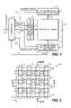
- FIG. 1illustrates in block diagram form a flash EEPROM system in which the various aspects of the present invention may be implemented
- FIG. 2is a plan view of a partially constructed dual floating gate memory cell array
- FIGS. 3A and 3Bare sectional views of one embodiment of the structure of FIG. 2 , taken at sections A-A and B-B thereof, respectively;
- FIG. 4is an equivalent circuit diagram of a dual floating gate memory cell of the array of FIGS. 2 , 3 A and 3 B;
- FIG. 5is a sectional view of another embodiment of the structure of FIG. 2 , taken at section A-A thereof;
- FIGS. 6 and 7are also sectional views of the structure of FIG. 2 , taken at section A-A thereof, which show modifications of the embodiment of FIG. 5 ;
- FIG. 8is a sectional view of another embodiment taken along a string of memory cells in a NAND array.
- FIG. 9is an equivalent circuit of the NAND string of FIG. 8 .
- FIG. 1An example memory system incorporating the various aspects of the present invention is generally illustrated in the block diagram of FIG. 1 .
- a large number of individually addressable memory cells 11are arranged in a regular array of rows and columns, although other physical arrangements of cells are certainly possible.
- Bit linesdesignated herein to extend along columns of the array 11 of cells, are electrically connected with a bit line decoder and driver circuit 13 through lines 15 .
- Word lineswhich are designated in this description to extend along rows of the array 11 of cells, are electrically connected through lines 17 to a word line decoder and driver circuit 19 .
- Steering gateswhich extend along columns of memory cells in the array 11 , are electrically connected to a steering gate decoder and driver circuit 21 through lines 23 .
- Each of the decoders 13 , 19 and 21receives memory cell addresses over a bus 25 from a memory controller 27 .
- the decoder and driving circuitsare also connected to the controller 27 over respective control and status signal lines 29 , 31 and 33 . Voltages applied to the steering gates and bit lines are coordinated through a bus 22 that interconnects the decoder and driver circuits 13 and 21 .
- the controller 27is connectable through lines 35 to a host device (not shown).
- the hostmay be a personal computer, notebook computer, digital camera, audio player, various other hand held electronic devices, and the like.
- the memory system of FIG. 1will commonly be implemented in a card according to one of several existing physical and electrical standards, such as one from the PCMCIA, the CompactFlashTM Association, the MMCTM Association, The SD Group and others.
- the lines 35terminate in a connector on the card which interfaces with a complementary connector of the host device.
- the electrical interface of many cardsfollows the ATA standard, wherein the memory system appears to the host as if it was a magnetic disk drive. Other memory card interface standards also exist.
- memory systems of the type shown in FIG. 1are permanently embedded in the host device.
- the decoder and driver circuits 13 , 19 and 21generate appropriate voltages in their respective lines of the array 11 , as addressed over the bus 25 , according to control signals in respective control and status lines 29 , 31 and 33 , to execute programming, reading and erasing functions. Any status signals, including voltage levels and other array parameters, are provided by the array 11 to the controller 27 over the same control and status lines 29 , 31 and 33 .
- a plurality of sense amplifiers within the circuit 13receive current or voltage levels that are indicative of the states of addressed memory cells within the array 11 , and provides the controller 27 with information about those states over lines 41 during a read operation.
- a large number of sense amplifiersare usually used in order to be able to read the states of a large number of memory cells in parallel.
- one row of cellsis typically addressed at a time through the circuits 19 for accessing a number of cells in the addressed row that are selected by the circuits 13 and 21 .
- all cells in each of many rowsare typically addressed together as a block for simultaneous erasure.
- the bit line decoder and driver circuit 13is connected through lines 15 with global bit lines, which are in turn selectively connected with the source and drain regions of the array.
- the sources and drains of columns of individual memory cellsare connected to proper programming voltages for either reading or programming in response to addresses supplied over the bus 25 and control signals over the lines 19 .
- the steering line decoder and driver circuit 21connects though lines 23 to the steering gates and is able to individually select steering lines and control their voltages in response to addresses provided on the bus 25 , control signals in the lines 33 , and data from the drivers and sense amplifiers 13 .
- the select gate decoder and driver circuit 19is connected with the word lines in order to individually select one row of the cell array. Individual cells within a selected row are then enabled for reading or writing by the bit line and steering gate decoder and driver circuits 13 and 21 .
- FIGS. 2 , 3 A and 3 BThe structure of an example NOR memory array formed on a single integrated circuit chip with the floating gates formed by a spacer technique is illustrated in FIGS. 2 , 3 A and 3 B, and an equivalent circuit of the resulting memory cell is given in FIG. 4 .
- a two-dimensional array of trenches 51 - 66are formed in a surface 49 of a semiconductor substrate 50 , preferably by initially etching long parallel trenches and then defining the shortened trenches 51 - 66 within them.
- trenchesare crossed by two sets of electrically conductive control gate lines, word lines 69 - 72 having lengths extending in the x-direction and steering gate lines 75 - 78 having lengths extending in the orthogonally oriented y-direction.
- an array of conductive shields 81 - 92are formed in recesses in the surface 49 of the substrate 50 between neighboring ones of the trenches 51 - 66 in the y-direction. Each shield is electrically connected with one of the steering lines 75 - 78 passing over it.
- These conductive shields and surrounding dielectricare periodically placed along initially formed elongated trenches to form the defined length trenches 51 - 66 in which the floating gates are positioned.
- FIGS. 3A and 3Bare cut-away views of FIG. 2 taken along orthogonally oriented sections A-A and B-B thereof, respectively.
- Each of the trenches 51 - 66includes memory cell floating gates, a select gate and layers of dielectric.
- a layer 101 of dielectric materialcovers the walls and bottom surface of the trench.
- the layer 101is preferably made of silicon dioxide (SiO 2 for example).
- Two conductive floating gates 103 and 105are formed as spacers along opposite sidewalls of the trench in the x-direction.
- the dielectric layer 107is preferably made of three layers, two layers of silicon dioxide on opposite sides of a layer of silicon nitride (Si 3 N 4 for example), in a structure commonly referred to as “ONO”. It will be noted that the ONO layer is confined to regions between the floating and steering gates, and avoids the channel areas. This improves the endurance of the memory cell and reduces noise and disturb phenomena that can be caused by its nitride layer trapping charge over time.
- the gates 103 , 105 and 109 , the dielectric layer 101 along the sidewalls and the intermediate dielectric layer 107together fill the trench 61 in the x-direction.
- a buried N+ diffusion 110is elongated in the y-direction and positioned under trenches 53 , 57 , 61 and 65 , providing source and drain regions for the memory cells of which they are a part.
- the remaining trenchesinclude the same structure and form.
- the neighboring trench 60includes floating gates 111 and 113 , a steering gate 115 and dielectric layers positioned in the same manner as in the trench 61 .
- a buried diffusion 117exists under the trench 60 and other trenches in the same column.
- the floating gatesare preferably formed by depositing polysilicon material over the entire memory cell array being formed including within the trenches, and then anisotropically etching that layer until the spacers, such as floating gate spacers 103 and 105 , remain within the trenches.
- a chemical-mechanical-polishing (CMP) stepmay be performed to remove any portion of the floating gate spacer material that may remain on the substrate surface 49 .
- the resulting floating gatesare positioned entirely within their respective trenches, below the substrate surface 49 .
- the steering gates 109 and 115are also conveniently positioned entirely within their trenches below the substrate surface 49 .
- Conductive control gate linesare positioned across the trenches, over the substrate surface 49 .
- the steering gate lines 75 - 78extend across the trenches in the y-direction, making contact with the steering gates in the trenches and conductive shields between the trenches.
- the line 77extends across and electrically contacts the steering gate 109 and the other steering gates in that column, as well as contacting the intermediate conductive shields 83 , 87 and 91 .
- An isolating layer of dielectric(not shown) will be positioned between the steering gate lines and any portions of the substrate surface 49 that are crossed by those lines. Dielectric material surrounds the steering gate lines.
- the line 77for example, has two dielectric layers 121 and 123 positioned on its top surface and coextensive with that surface.
- the layer 121is preferably made of silicon dioxide and the layer 123 of silicon nitride. Spacers 125 and 127 are formed along the sidewalls in the x-direction of the conductive line 77 and dielectric strips 121 and 123 on top of the line 77 .
- the word lines 69 - 72are positioned across the dielectric enclosed steering gate lines, perpendicular thereto. Because of the thicknesses of the intermediate dielectric, there is little or no coupling between the word and steering gate lines.
- the word linesare further separated from the substrate surface between the trenches in the x-direction by a layer 129 of gate dielectric, preferably silicon dioxide. Regions of the word lines adjacent the gate dielectric 129 form select gates of the memory cells. Channel regions of select transistors exist in the substrate surface 49 on opposite sides of the gate dielectric layers 129 between trenches.
- the shieldsare surrounded by dielectric, such as layers 131 and 132 along sidewalls of the shield 91 that separate it from edges of the floating gates on either side in the y-direction and a layer 133 between a bottom surface of the shield 91 and the substrate surface 49 .
- the bottom layer 133is made relatively thick to minimize coupling between the shield 91 and the substrate surface 49 .
- the side layers 131 and 132are made relatively thin to maximize coupling between the shield 91 and edges of the floating gates on either side of the shield. Since the shield 91 is electrically connected with the steering gate line 77 , this provides an increased area of coupling between each steering gate and the floating gates in the same column as the steering gate.
- Memory cells with an increased coupling ratiocouple a larger percentage of the voltage placed on a steering gate to a floating gate with which it is capacitively coupled.
- coupling between the floating gates and the buried bit line diffusionscan be kept small, as can be seen from FIG. 3A , because of the thin floating gates in the x-direction.
- One specific example configuration for array of FIGS. 2 , 3 A and 3 Bincludes continuous trenches formed in the substrate in both the x- and y-directions, thus crossing each other.
- the floating and steering gatesare positioned in the trenches elongated in the y-direction between the x-direction trenches.
- the shielding elementsare positioned in the trenches elongated in the x-direction where they intersect with the y-direction trenches.
- a suitable field dielectric materialthen fills the x-direction trenches between the shielding elements.
- the example structure of FIGS. 2 , 3 A and 3 Butilizes doped polysilicon or other suitable conductive material formed from five separate depositions of material at different points in the process.
- the floating gatesare formed from one, the steering gates from the second, the shielding elements from the third, the steering gate lines from the fourth and the word lines from the fifth deposition of conductive material.
- the polysiliconmay be doped while being deposited, or, alternatively, may be deposited without doping and then ions implanted after the deposition.
- the last layer of polysilicon from which the word lines are formedmay be silicided in order to reduce the resulting word line resistance, or have metal bonded to its top surface for this purpose. Alternatively, the word lines may be formed entirely from a metal as the fifth layer.
- FIG. 4is an equivalent circuit of one memory cell of FIGS. 3A and 3B , the same reference numbers being used with a prime (′) added.
- Three transistorsare connected in series between the buried bit line diffusions 110 ′ and 117 ′.
- a storage transistor on the leftincludes the floating gate 113 ′ and the storage transistor on the right contains the floating gate 103 ′. In between these storage transistors is a select transistor having a control gate 71 ′.
- the array of memory cells illustrated heremay be operated in essentially the same manner as the dual floating gate memory cell array of the aforementioned U.S. Pat. No. 6,151,248.
- the substrate channel of this one memory cellis divided into three segments.
- One segment (T 1 -left)is along a vertical sidewall of the trench 60 adjacent to the floating gate 113 , between the diffusion 117 and the substrate surface 49 . This is part of the left storage transistor of the memory cell being described.
- the next segment (T 2 )is along the substrate surface 49 between walls of neighboring trenches 60 and 61 .
- the third segment (T 1 -right)is along a vertical sidewall of the trench 61 .
- the trenchesmay be formed as small in x- and y-dimensions across the substrate surface as the processing allows. The result is a very compact array of memory cells in the x-direction across the substrate surface.
- the amount of integrated circuit area per memory cellis thus made very small.
- the density of memory cellsis potentially doubled from the case where the floating gates are positioned across the substrate surface, given the same processing scale.
- the select gate channel length (T 1 distance)may be increased slightly and the floating gate channel length (T 1 ) may be significantly increased.
- the preferred programming mechanism for the memory cells shown in FIGS. 3A and 3Bis ballistic programming. That is, electrons are accelerated within the T 2 region of the channel in a direction substantially parallel to the substrate surface 49 by appropriate voltages being applied to the word lines, select gate lines, the buried bit line diffusions and the substrate.
- the path of the high velocity electronsstrikes one of the floating gates 103 or 113 substantially perpendicularly to its broad planar surface, depending upon which floating gate is being programmed.
- the programming efficiencyis potentially orders of magnitude higher than the more standard source side injection. It is preferable that no part of the floating gate overlaps the substrate surface 49 in the T 2 region, thereby freeing the T 2 region of field effects that can interfere with this direct high energy electron path.
- the sidewalls of the trenches as shown in FIG. 3Aare preferably vertical (perpendicular to the substrate surface 49 ), as shown, for the most efficient ballistic programming, but may alternatively be sloped somewhat if that is more convenient for other reasons.
- a high erase voltageis placed on the word line for this.
- a floating gatemay be erased to its vertical channel portion through the floating dielectric layer along a vertical face of the trench. For this, a voltage in the range of zero to ⁇ 0.5 volts is applied to the bit line (alternatively the bit line can be allowed to float to prevent the possibility of also erasing to the bit line), zero volts is applied to the substrate and up to ⁇ 20 volts is applied on the steering gate.
- Another possibilityis to erase between the bottom of a floating gate and a buried diffusion bit line under the bottom of the trench, through the floating gate dielectric layer on the bottom of the trench.
- Example voltagesinclude 5 volts on the bit line, 0 volts on the substrate and up to ⁇ 15 volts on the steering gate. This last alternative has an advantage of not erasing through either of the floating gate or select gate dielectric layers, thus avoiding trapping charge in these layers over time from many erase operations that will usually affect programming and reading.
- the memory cell array of FIGS. 2 , 3 A and 3 Bprovides shielding between neighboring floating gates in both the x- and y-directions. Since the steering gates extend between floating gates in the same trench to the bottom of the trench, the steering gates provide shielding in the x-direction. In the y-direction, the shielding elements 81 - 92 provide such isolation. The field coupling of charge on one floating gate to a neighboring floating gate, which can be a source of read errors, is thereby significantly reduced.
- An early stepis the implantation of ions, such as of boron, into a blank substrate from the surface upon which the array is to be formed.
- ionssuch as of boron
- Several implants of various energies and dosesallow control of the doping level along the resulting vertical channel portions T 1 .
- the vertical orientation of the floating gate portions of the channelallows such selective doping along the channel length to be accomplished with relative ease and reliable results. It may be desirable, for example, to provide the highest ion concentration at a depth that coincides with the midway point along the floating gate channel length T 1 .
- a negative ion gradient with increasing depthmay be installed near the substrate surface, which is beneficial for enhancing generation of hot electrons used during programming. Further, control of the doping level at the corners of the channels, where gaps exist between the select gates and the floating gates, can result in the gaps not dominating behavior of the memory cell.
- a thin silicon oxide layeris grown over the region of the surface of the substrate where the array is being formed. This serves as a buffer for a layer of silicon nitride that is next deposited over the oxide layer.
- the nitride layeris then masked and etched into a pattern of strips having lengths extending in the y-direction, preferably with a minimum width and spacing between them in the x-direction as is possible with the lithography and other aspects of the particular process being used. Areas of the substrate surface and thin oxide layer between the nitride strips are then anisotropically etched away with the nitride strips serving as a mask.
- Trenches with substantially vertical wallsare formed in the substrate by this etching step to a depth slightly greater than the desired floating gate vertical channel length T 1 .
- Each column of the trenches 51 - 66 ( FIG. 2 )is eventually formed in one of these trenches.
- a thick layer of oxideis then isotropically deposited over the entire region of the array over the nitride strips and into the trenches.
- This oxide layeris then anisotropically etched to leave oxide spacers along the common sidewalls of the trenches and nitride strips.
- the thickness of the deposited oxide layer and the etchingare chosen to leave a narrow space between the spacers in the x-direction.
- These spacers and nitride stripsate then used as an implant mask. Buried N+ implants, using arsenic for example, of various energies are made into the bottoms of the trenches through this mask between the spacers.
- bit line diffusionsare thus formed as strips extending along the bottoms of the trenches in the y-direction.
- the implanted ionslater diffuse outward in the x-direction as a result of further processing steps at elevated temperatures, forming the bit line diffusions 110 , 117 et al. shown in FIGS. 3A and 3B .
- a first polysilicon layer(Poly 1 ) is then isotropically deposited over the array area to a thickness of from 10 nm to 20 nm. This layer is then anisotropically etched back to leave spacer strips that extend continuously along the trench sidewalls in the y-direction and are spaced apart in the x-direction within the trenches. Portions of the lengths of these polysilicon strips are later removed to leave the spacer floating gates of the array.
- An ONO layeris then formed over the array area, the portions over the polysilicon spacer strips that remain as floating gates forming the inter-poly dielectric layer 107 of FIGS. 3A and 3B .
- a 5-6 nm thick oxide layeris first deposited, grown or both.
- a 5-7 nm nitride layeris then deposited over the oxide layer.
- a final 5-6 nm thick oxide layeris then grown, deposited or both over the nitride layer.
- a high temperature oxide densification stepmay be performed after forming each of the oxide layers. Alternatively, this may be omitted if later high temperature annealing steps are included in the process as they also perform the densification task.
- a second layer of polysilicon(Poly 2 ) is isotropically deposed over the array area to a thickness sufficient to completely fill the trenches between the ONO coated strips of Poly 1 .
- a CMP stepis then performed to remove all material down to the substrate surface. This leaves strips of Poly 2 extending in the y-direction, which, when later separated, form the steering gates 109 , 115 et al. of FIGS. 3A and 3B .
- the next several stepsform a nitride mask and use that mask to etch the Poly 1 and Poly 2 strips, the dielectric layers surrounding them and the substrate in strips having lengths extending in the x-direction.
- the depth of the resulting x-direction trenchesis preferably the same as the earlier floating gate trenches etch.
- a non-preferential etchis preferred so that each of Poly 1 , Poly 2 , oxide layer, ONO layer and silicon substrate are etched at about the same rate. It is in these trenches that the shielding elements 51 - 66 ( FIG. 2 ) are later formed. This etch separates the Poly 1 and Poly 2 strips as shown in FIGS. 3A and 3B .
- the steering gate lines 75 - 78FIGS. 2 , 3 A and 3 B are later formed to connect them together in columns.
- a dielectric layeris formed over the array area, such as by both growing an oxide layer and isotropically depositing oxide to result in the dielectric layers 131 , 132 and 133 ( FIG. 3B ) of unequal thicknesses within the x-direction trenches.
- a third layer of polysilicon(Poly 3 ) is then deposited over this oxide, into the x-direction trenches.
- the areais then again subjected to CMP to remove the polysilicon and oxide down to the substrate surface. Remaining are strips of Poly 3 extending in the x-direction, wholly within the x-direction trenches, and the oxide that separates the Poly 3 strips from the substrate trench walls. These Poly 3 strips are later separated to leave the shields 81 - 92 .
- the lengths of the resulting shields in the x-directionbe greater than the widths of the adjacent trenches 51 - 66 , as is the case in the plan view of FIG. 2 , although they could alternatively be made the same size.
- an etch maskis first formed over the array area with openings according to the process line width aligned over the regions of the Poly 3 strips to be removed. Spacers are then formed along at least the edges of these openings in the y-direction to narrow the opening. Portions of the Poly 3 strips exposed through these restricted openings are then removed by an anisotropic etching step, thereby leaving the individual shields 81 - 92 .
- a next series of stepsforms the steering gate lines 75 - 78 .
- a fourth layer of polysilicon(Poly 4 ) is deposited over the area of the array.
- An etch maskis then formed over the Poly 4 layer in the form of strips extending in the y-direction to cover portions of the layer that are to remain and become lines 75 - 78 . Since this mask is not aligned with other elements previously formed, it is desirable to make the widths of the remaining Poly 4 strips narrower than the line width of the process. Some degree of misalignment in the x-direction can then be tolerated.
- These narrow mask openingsmay be obtained by first forming an oxide mask over the Poly 4 layer with strips having widths and spaces between them in the x-direction equal to the minimum line width of the process being used. Spacers of oxide material are then formed along the edges of the openings to narrow them. A nitride layer is then deposited over the oxide material and onto the Poly 4 layer through the narrowed openings between the oxide spacers. This structure is then subjected to CMP down to the oxide material, thereby leaving nitride strips extending in the y-direction with widths of the desired steering gate lines. The oxide material between the nitride strips is then removed by a selective etch. The Poly 4 layer is then anisotropically etched through the resulting nitride mask to remove material from the Poly 4 layer except where the nitride strips exist. The result is the steering gate lines 75 - 78 .
- the nitride masking stripsare preferably left in place on the Poly 4 strips, as shown in FIGS. 3A and 3B .
- Oxide spacersare then formed along sides of the stack of Poly 4 and nitride strips in order to provide sufficient isolation between the Poly 4 strips (steering gate lines) and the word lines to be formed over them.
- the added height to the stack provided by the nitride layerresults in the spacers ( 125 , 127 et al. of FIG. 3A ) to reach a sufficient thickness in the region of the Poly 4 strip (steering gate line 77 et al. of FIG. 3A ).
- a layer of oxideis grown, deposited or both, in order to form the select gate dielectric layer 129 ( FIG. 3A ) on the exposed surface of the substrate.
- a fifth layer of polysilicon(Poly 5 ) is then deposited over the array area from which the word lines 69 - 72 are formed.
- the Poly 5 layermay be separated into word lines narrower than the minimum line width of the processing being used in the same manner as described above for forming the narrow steering gate lines 75 - 78 from the Poly 4 layer.
- This maskis, of course, oriented with its strips extending in the x-direction. This process of narrowing the widths of the resulting polysilicon strips then allows some misalignment of the resulting Poly 5 lines in the y-direction.
- Further stepsinclude forming a first set of metal lines separated by dielectric layers that are periodically connected to the polysilicon steering gate lines 75 - 78 along their lengths, and a second set of metal lines connected along the lengths of the word lines 69 - 72 , according to standard processing technology.
- FIG. 5is a cross-sectional view corresponding to that of FIG. 3A for the embodiment described above. Elements of the structure shown in FIG. 5 that are the same or essentially the same are identified by the same reference numbers as in FIG. 3A , and different elements with the same reference number as their counterparts but with a double prime (′′) added.
- a primary advantage of the embodiment of FIG. 5is that the lengths of the substrate channel portions T 1 -left and T 1 -right opposite the floating gates of the memory cell are reduced without reducing the coupling area between the floating gates and the steering gate if these gates remain the same size.
- Thisdesirably increases the cell's floating gate to steering gate coupling ratio, since the amounts of capacitive coupling between each of the floating gates and the substrate are in the denominator of that ratio and the level of coupling between the floating and steering gates is in the numerator.
- the select transistor channel length T 2need not be affected.
- FIG. 5 structureAnother advantage of the FIG. 5 structure is the increased overlap between each of the floating gates and the word line. More area of the floating gate 113 , for example, lies opposite the word line 71 ′′. This makes it possible to increase the coupling between the floating gates and the word lines, depending upon the nature and thickness of the dielectric therebetween. This allows the word lines to be used to couple voltages to the floating gates during erase either to the buried bit line diffusion or to the substrate channel, thereby enhancing erase. The word lines may then also be used to assist in controlling the voltage of the floating gates during programming, such as by providing a minimum floating gate voltage required to initiate programming of the floating gates in the row of a word line.
- the steering gate linessuch as the line 76
- the steering gate linesextend across the array in the y-direction, in electrical contact with the steering gates and intermediate shielding elements it crosses, such as the steering gate 115 and the shielding elements 86 and 90 ( FIG. 2 ) on either side of the trench 60 ( 60 ′′ in FIG. 5 ) that contains the steering gate 115 .
- the shielding elementsare formed with top surfaces at or below the substrate surface 49 (see FIG. 3B )
- the raised gate structure of FIG. 5causes the steering gate lines 76 etc. to rise up over the steering gates 115 etc. and then down on both sides of the steering gates in the y-direction to electrically contact the shielding elements 90 etc.
- the modified array of FIG. 5may be made by the process described above for the array of FIGS. 2 , 3 A and 3 B, with certain modifications.
- the nitride mask formed in an early step on the substrate surfaceis left in place as the first polysilicon layer (Poly 1 ) is deposited.
- This nitride maskis used to etch trenches into the silicon surface, which in this modification are not made as deep as before.
- the thicknesses of the nitride mask strips, which extend in the y-direction and cover the select gate regions of the memory cells,are controlled to be equal to a dimension h, the desired distance between the top of the floating/steering gate structure and the substrate surface 49 .
- Poly 1is then deposited over the nitride mask strips and into the substrate trenches and their vertical extension formed by the nitride strips.
- the floating gate spacers that result from the anisotropic etch of the Poly 1 layerthen extend to the top of the nitride strips, above the substrate surface by the distance h.
- the nitride mask stripsare then later removed.
- the buried bit line diffusionsmay be implanted at this time, using the nitride strips and floating gates as an implant mask. Since the floating gates narrow the width of the trenches through which ions are implanted, the oxide spacers formed in the above description of the FIGS. 3A and 3B process before the Poly 1 is deposited are not necessary. The added steps required to form and remove those oxide spacers can then be omitted.
- FIG. 5If it is desired to have the steering to floating gate coupling ratio increased but maintain a word line (select gate) to floating gate coupling ratio low, the word line and its select gate structure shown in FIG. 5 may be changed. Three different examples of select gate structures that reduce the coupling area with the floating gates are shown in FIGS. 6 and 7 , wherein elements that are the same or essentially the same as those shown in FIG. 5 are identified by the same reference numbers. While reducing coupling with the floating gates, the select gate channel length T 2 need not be reduced.
- select gatessuch as gates 135 and 137 , are individually formed of a conductive material such as doped polysilicon. These select gates are then later connected together by a horizontal word line conductor 139 extending in the x-direction along a row of memory cells and downward extending conductors 141 and 143 that contact the individual select gates.
- the area of coupling with the floating gates, along vertical edges of the select gates,can be kept small since thin select gates can be formed.
- the vertical portions 141 , 143 et al.can also be made of doped polysilicon while the horizontal portion 139 is made of a metal.
- all of the word line portions 139 , 141 , 143 et al.can be made of metal.
- FIG. 7shows a further modification wherein thin select gates 147 and 149 are formed, as in FIG. 6 , followed by separately forming second layers 151 and 153 having a triangular shape in this cross-section.
- the triangular portionsare oriented with surfaces adjacent the upper narrow edges of the floating gates, with a thin layer of dielectric between them, which facilitates erasing the floating gates to the select gates. But at the same time the coupling between the select and floating gates is minimized.
- the individual select gate structuresare then connected by conductive word lines, such as the word line 155 , which is preferably a metal, including portions descending downward to contact the select gate structures.
- FIGS. 2-7are described as utilizing dual-gate memory cells connected in a NOR architecture, as specific examples, it will be understood that the trench gate structures described may also be utilized in other memory cell array configurations.
- FIG. 8a cross-section through a portion of a NAND string of series connected memory cells. Formed in a surface 159 of a semiconductor substrate 161 are a series of trenches 163 , 165 , 167 and 169 . Two floating gates are formed in each trench of spacers of doped polysilicon material (from Poly 1 ), in the manner described above, after a dielectric layer is formed on the sidewalls and bottom of the trench. Eight such floating gates 171 - 178 are included in the illustration of FIG. 8 . After formation of the spacer floating gates, source and drain diffusions 181 - 189 are formed by ion implantation. Alternatively, the ion implantation may take place before the floating gates are deposited but after the trenches are formed.
- word line control gatesare formed to extend across the array in a direction perpendicular to that of the memory cell string. Indeed, the array is made up of a large number of such strings in parallel columns with the word lines extending across the strings along rows of memory cells. Since there is a separate word line crossing each floating gate, two such word lines need to be formed in each of the trenches 163 , 165 , 167 and 169 , rather than the single steering gate of the earlier described embodiments.
- the word linesare formed from two layers of polysilicon that are deposited and etched in sequence.
- a first word line layer of polysilicon(Poly 2 ) covers the entire array including extending into the trenches between the floating gates.
- a mask formed over the Poly 2 layerallows its removal in a pattern that leaves a first set of word lines 191 - 194 , every other word line along the memory cell string.
- the next layer of polysilicon(Poly 3 ) is deposited over the array including into the remaining space of the trenches.
- the Poly 3 layeris then masked and etched to leave a second set of word lines 197 - 201 that are the remaining word lines of the array.
- the size of the trenches in a direction along the stringmay in some cases need to be larger than the smallest resolution element of the process being used.
- FIG. 9An electrical equivalent circuit of the NAND memory cell string of FIG. 8 is given as FIG. 9 , wherein corresponding elements are given the same reference number with a prime (′) added.
- corresponding elementsare given the same reference number with a prime (′) added.
- At the ends of each stringare typically switching transistors 205 and 207 to selectively connect the string to its global bit line and a reference potential such as ground.
Landscapes
- Non-Volatile Memory (AREA)
- Semiconductor Memories (AREA)
Abstract
Description
- This application is related to an application being filed concurrently herewith by Nima Mokhlesi, entitled “Method of Making an Array of Non-Volatile Memory Cells With Floating Gates Formed of Spacers in Substrate Trenches” which application is incorporated herein in its entirety by this reference.
- This invention relates generally to non-volatile flash memory systems, and, more specifically, to a structure and process of forming arrays of memory cells that utilize substrate trenches to reduce the overall size of the arrays.
- There are many commercially successful non-volatile memory products being used today, particularly in the form of small form factor cards, which use an array of flash EEPROM (Electrically Erasable and Programmable Read Only Memory) cells. Arrays with either a NOR or a NAND architecture are commonly used. One or more integrated circuit chips containing a memory cell array are commonly combined with a controller chip to form a complete memory system. Alternatively, part or all of the controller function may be implemented on the same chip that contains all or part of the memory cell array.
- In one type of NOR array, each memory cell has a “split-channel” between source and drain diffusions. The floating gate of the cell is positioned over one portion of the channel and the word line (also referred to as a control gate) is positioned over the other channel portion as well as over the floating gate. This effectively forms a cell with two transistors in series, one (the memory transistor) with a combination of the amount of charge on the floating gate and the voltage on the word line controlling the amount of current that can flow through its portion of the channel, and the other (the select transistor) having the word line alone serving as its gate. The word line extends over a row of floating gates. Examples of such cells, their uses in memory systems and methods of manufacturing them are given in U.S. Pat. Nos. 5,070,032, 5,095,344, 5,315,541, 5,343,063, and 5,661,053, and 6,281,075.
- A modification of this split-channel flash EEPROM cell adds a steering gate positioned between the floating gate and the word line. Each steering gate of an array extends over one column of floating gates, perpendicular to the word lines. The effect is to relieve the word line from having to perform two functions at the same time when reading or programming a selected cell. Those two functions are (1) to serve as a gate of a select transistor, thus requiring a proper voltage to turn the select transistor on and off, and (2) to drive the voltage of the floating gate to a desired level through an electric field (capacitive) coupling between the word line and the floating gate. It is often difficult to perform both of these functions in an optimum manner with a single voltage. With the addition of the steering gate, the word line need only perform function (1), while the added steering gate performs function (2). The use of steering gates in a flash EEPROM array is described, for example, in U.S. Pat. Nos. 5,313,421 and 6,222,762.
- In one specific type of memory cell that efficiently utilizes integrated circuit area, two floating gates are included, each of which may be operated in binary (one bit per floating gate) or with multiple programming states (more than one bit per floating gate). The two floating gates are positioned over the substrate channel between source and drain diffusions with a select transistor in between them. A steering gate is included along each column of floating gates and a word line is provided thereover along each row of floating gates. When accessing a given floating gate for reading or programming, the steering gate over the other floating gate of the cell containing the floating gate of interest is raised sufficiently high to turn on the channel under the other floating gate no matter what charge level exists on it. This effectively eliminates the other floating gate as a factor in reading or programming the floating gate of interest in the same memory cell. For example, the amount of current flowing through the cell, which can be used to read its state, is then a function of the amount of charge on the floating gate of interest but not of the other floating gate in the same cell.
- Examples of an array with dual floating gate memory cells, and operating techniques therefore, are described in U.S. Pat. Nos. 5,712,180, 6,103,573 and 6,151,248. The dual floating gate memory cell arrays are usually formed entirely on a surface of a semiconductor substrate. However, U.S. Pat. No. 6,151,248 additionally describes, primarily with respect to
FIGS. 6 and 7 thereof, memory cells formed in a trench in the substrate surface and along surface areas of the substrate adjacent to the trench. U.S. Pat. No. 6,936,887 also describes an array of memory cells partially formed in substrate trenches. - The NAND array utilizes series strings of more than two memory cells, such as16 or32, connected along with one or more select transistors between individual bit lines and a reference potential to form columns of cells. Word lines extend across cells in a row direction, across a large number of these columns. An individual cell within a column is read and verified during programming by causing the remaining cells in the string to be turned on hard so that the current flowing through a string is dependent upon the level of charge stored in the addressed cell. Examples of NAND architecture arrays and their operation as part of a memory system are found in U.S. Pat. Nos. 5,570,315, 5,774,397, 6,046,935, 6,522,580, 6,888,755 and 6,925,007.
- There are various programming techniques for causing electrons to travel through the gate dielectric from the substrate onto the floating gate. The most common programming mechanisms are described in a book edited by Brown and Brewer, “Nonvolatile Semiconductor Memory Technology,” IEEE Press, section 1.2, pages 9-25 (1998). One technique, termed “Fowler-Nordheim tunneling” (section 1.2.1), causes electrons to tunnel through the floating gate dielectric under the influence of a high field that is established thereacross by a voltage difference between the control gate and the substrate channel. Another technique, channel hot electron injection in the drain region, commonly referred to as “hot-electron injection” (section 1.2.3), injects electrons from the cell's channel into a region of the floating gate adjacent the cell's drain. Yet another technique, termed “source side injection” (section 1.2.4), controls the substrate surface electrical potential along the length of the memory cell channel in a manner to create conditions for electron injection in a region of the channel away from the drain. Source side injection is also described in an article by Kamiya et al., “EPROM Cell with High Gate Injection Efficiency,” IEDM Technical Digest, 1982, pages 741-744, and in U.S. Pat. Nos. 4,622,656 and 5,313,421. In a farther programming technique, termed “ballistic injection” high fields are generated within a short channel to accelerate electrons directly onto the charge storage element, as described by Ogura et al., “Low Voltage, Low Current, High Speed Program Step Split Gate Cell with Ballistic Direct Injection for EEPROM/Flash”, IEDM 1998, pages 987-990.”
- One of two techniques for removing charge from floating gate charge storage elements to erase memory cells are primarily used in both of the two types of memory cell arrays described above. One is to erase to the substrate by applying appropriate voltages to the source, drain, substrate and other gate(s) that cause electrons to tunnel through a portion of a dielectric layer between the floating gate and the substrate.
- The other erase technique transfers electrons from the floating gate to another gate through a tunnel dielectric layer positioned between them. In the first type of cell described above, a third gate is provided for that purpose. In the second type of cell described above, which already has three gates because of the use of a steering gate, the floating gate is erased to the word line, without the necessity to add a fourth gate. Although this later technique adds back a second function to be performed by the word line, these functions are performed at different times, thus avoiding the necessity of making compromises to accommodate the two functions. When either of these erase techniques is utilized, a large number of memory cells are grouped together into blocks of a minimum number of cells that are simultaneously erased, in a “flash.” In one approach, the individual blocks include enough memory cells to store the amount of user data stored in a disk sector, namely 512 bytes, plus some overhead data. Erasure of a number of blocks at once, defect management and other flash EEPROM system features are described in U.S. Pat. No. 5,297,148. In another approach, each group contains enough cells to hold several thousand bytes of user data, equal to 8, 16 or more host sectors' worth of data that are individually programmable and readable. Examples of operating such a large block memory are given in U.S. Pat. No. 6,968,421.
- In place of electrically conductive floating gates, some flash memories utilize a non-conductive dielectric material that traps electrons. In either case, an individual memory cell includes one or more charge storage elements. Examples of the use of dielectric are described in aforementioned U.S. Pat. No. 6,925,007 and documents referenced therein. In the case of a dielectric trapped charge memory cell, two or more charge storage elements may be formed as two or more regions of a single continuous layer of dielectric that are spaced apart thereacross. One example of a suitable charge storage dielectric material is a three-layer oxide-nitride-oxide (ONO) composite. Another example is a single layer of silicon rich silicon dioxide material. As in almost all integrated circuit applications, the pressure to shrink the silicon substrate area required to implement some integrated circuit function also exists with flash EEPROM systems. It is continually desired to increase the amount of digital data that can be stored in a given area of a silicon substrate, in order to increase the storage capacity of a given size memory card and other types of packages, or to both increase capacity and decrease size. Another way to increase the storage density of data is to store more than one bit of data per memory cell. This is accomplished by dividing a window of a memory cell threshold voltage range into more than two states. The use of four such states allows each charge storage element to store two bits of data, eight states stores three bits of data per charge storage element, and so on. A multiple state flash EEPROM structure and operation is described in U.S. Pat. Nos. 5,043,940 and 5,172,338, as examples.
- An array of floating gate charge storage element memory cells is formed with the use of trenches or cavities in which the floating gates are positioned along sidewalls thereof, having a gate dielectric therebetween, and without overlying the substrate surface adjacent the trenches. That is, the floating gates remain within the area of the trenches in plan view. This is preferably accomplished by utilizing spacers as the floating gates, wherein a layer of floating gate material, such as conductively doped polysilicon, is isotropically deposited over the array and into the trenches, followed by anisotropically etching away all of the deposited floating gate material except for spacers that remain along the trench sidewalls. Conductive control gates can then be formed in the trenches between the floating gate spacers, and/or select transistors can be positioned in substrate surface areas adjacent the trenches, depending upon the exact configuration desired for the memory cells.
- An overall advantage of this structure is its efficient use of substrate surface area. A significant portion of the length of the memory cell channel is vertically oriented along the trench walls, thus reducing the amount of substrate surface area required for each memory cell. Source and drain regions may be implanted into the bottoms of the trenches between the floating gates therein. This floating gate structure and method of forming floating gates may be used in a wide variety of types of flash memory arrays. If used to form a NOR array of dual floating gate memory cells, for example, each such cell is formed from two floating gates along sidewalls of adjacent trenches and a select transistor formed therebetween in the substrate surface. If used to form a NAND array, the series strings of memory cell transistors are formed along the trench sidewalls with connecting diffusions in the bottoms of the trenches between the floating gates therein and along the substrate surface between adjacent trenches.
- One specific advantage of this positioning of floating gates along the walls of substrate trenches is that, in memory architectures where appropriate, the floating gates may be programmed by ballistic injection with increased efficiency. That is, electrons may be accelerated along the lengths of the substrate channels between trenches and parallel to the substrate surface onto the floating gates in a direct line path, impinging at a normal or near normal angle to an interface between the substrate trench sidewall and the tunnel dielectric sandwiched between the floating gate and the sidewall. Therefore, it is not necessary that the electrons be redirected by a scattering mechanism, which scattering occurs during use of the more usual source side injection and hot-electron injection programming mechanisms. By avoiding wrapping the floating gates out of the trenches and along the substrate surface, and by applying a voltage to the select gate that is slightly higher than the select gate's VT, a high lateral electric field is created which accelerates the channel electrons to kinetic energies sufficient to overcome the tunnel oxide barrier. Many of these hot electrons will impinge on the tunnel oxide without having to be first scattered in order to re-direct their momentum. The high voltage on the floating gate may also help accelerate the electrons along a path to the floating gate as they traverse the channel region. The walls of the trenches along which the floating gates are formed may be perpendicular to the substrate surface, which is optimum for efficient programming by ballistic injection and allows the size of the memory cell to be minimized, but this is not a requirement. Substrate trenches with perpendicular sidewalls are conveniently formed by anisotropically etching into the substrate surface.
- Rather than forming floating gates as the memory cell charge storage elements, a dielectric charge trapping material may be substituted. The middle nitride layer of ONO, for example, can be deposited by use of the same spacer techniques. Uniform thickness layers of oxide are formed in a manner to be on either side of the nitride spacer to provide the ONO structure. Alternatively, spacers of silicon rich silicon dioxide can be formed in the same manner as the conductive floating gates, and the dielectric layers provided on either side of the floating gates need not be formed on such dielectric spacers.
- Additional aspects, advantages, embodiments and features of the present invention are included in the following description of exemplary examples thereof, whose description should be taken in conjunction with the accompanying drawings.
- All patents, patent applications, articles, book portion, other publications, documents and things referenced herein are hereby incorporated herein by this reference in their entirety for all purposes. To the extent of any inconsistency or conflict in the definition or use of terms between any of the incorporated publications, documents or things and the present application text, those of the present application text shall prevail.
FIG. 1 illustrates in block diagram form a flash EEPROM system in which the various aspects of the present invention may be implemented;FIG. 2 is a plan view of a partially constructed dual floating gate memory cell array;FIGS. 3A and 3B are sectional views of one embodiment of the structure ofFIG. 2 , taken at sections A-A and B-B thereof, respectively;FIG. 4 is an equivalent circuit diagram of a dual floating gate memory cell of the array ofFIGS. 2 ,3A and3B;FIG. 5 is a sectional view of another embodiment of the structure ofFIG. 2 , taken at section A-A thereof;FIGS. 6 and 7 are also sectional views of the structure ofFIG. 2 , taken at section A-A thereof, which show modifications of the embodiment ofFIG. 5 ;FIG. 8 is a sectional view of another embodiment taken along a string of memory cells in a NAND array; andFIG. 9 is an equivalent circuit of the NAND string ofFIG. 8 .- An example memory system incorporating the various aspects of the present invention is generally illustrated in the block diagram of
FIG. 1 . A large number of individuallyaddressable memory cells 11 are arranged in a regular array of rows and columns, although other physical arrangements of cells are certainly possible. Bit lines, designated herein to extend along columns of thearray 11 of cells, are electrically connected with a bit line decoder anddriver circuit 13 throughlines 15. Word lines, which are designated in this description to extend along rows of thearray 11 of cells, are electrically connected throughlines 17 to a word line decoder anddriver circuit 19. Steering gates, which extend along columns of memory cells in thearray 11, are electrically connected to a steering gate decoder anddriver circuit 21 throughlines 23. Each of thedecoders bus 25 from amemory controller 27. The decoder and driving circuits are also connected to thecontroller 27 over respective control andstatus signal lines bus 22 that interconnects the decoder anddriver circuits - The
controller 27 is connectable throughlines 35 to a host device (not shown). The host may be a personal computer, notebook computer, digital camera, audio player, various other hand held electronic devices, and the like. The memory system ofFIG. 1 will commonly be implemented in a card according to one of several existing physical and electrical standards, such as one from the PCMCIA, the CompactFlash™ Association, the MMC™ Association, The SD Group and others. When in a card format, thelines 35 terminate in a connector on the card which interfaces with a complementary connector of the host device. The electrical interface of many cards follows the ATA standard, wherein the memory system appears to the host as if it was a magnetic disk drive. Other memory card interface standards also exist. Alternatively to the card format, memory systems of the type shown inFIG. 1 are permanently embedded in the host device. - The decoder and
driver circuits array 11, as addressed over thebus 25, according to control signals in respective control andstatus lines array 11 to thecontroller 27 over the same control andstatus lines circuit 13 receive current or voltage levels that are indicative of the states of addressed memory cells within thearray 11, and provides thecontroller 27 with information about those states overlines 41 during a read operation. A large number of sense amplifiers are usually used in order to be able to read the states of a large number of memory cells in parallel. During reading and program operations, one row of cells is typically addressed at a time through thecircuits 19 for accessing a number of cells in the addressed row that are selected by thecircuits - The bit line decoder and
driver circuit 13 is connected throughlines 15 with global bit lines, which are in turn selectively connected with the source and drain regions of the array. The sources and drains of columns of individual memory cells are connected to proper programming voltages for either reading or programming in response to addresses supplied over thebus 25 and control signals over thelines 19. - The steering line decoder and
driver circuit 21 connects thoughlines 23 to the steering gates and is able to individually select steering lines and control their voltages in response to addresses provided on thebus 25, control signals in thelines 33, and data from the drivers andsense amplifiers 13. - The select gate decoder and
driver circuit 19 is connected with the word lines in order to individually select one row of the cell array. Individual cells within a selected row are then enabled for reading or writing by the bit line and steering gate decoder anddriver circuits - Operation of a memory system such as illustrated in
FIG. 1 is further described in patents identified in the Background section above, and in other patents assigned to SanDisk Corporation, assignee of the present application. In addition, U.S. Pat. No. 6,738,289 describes an example data programming method. - The structure of an example NOR memory array formed on a single integrated circuit chip with the floating gates formed by a spacer technique is illustrated in
FIGS. 2 ,3A and3B, and an equivalent circuit of the resulting memory cell is given inFIG. 4 . Referring primarily to the plan view ofFIG. 2 , a two-dimensional array of trenches51-66 are formed in asurface 49 of asemiconductor substrate 50, preferably by initially etching long parallel trenches and then defining the shortened trenches51-66 within them. These trenches are crossed by two sets of electrically conductive control gate lines, word lines69-72 having lengths extending in the x-direction and steering gate lines75-78 having lengths extending in the orthogonally oriented y-direction. Optionally but preferably, an array of conductive shields81-92 are formed in recesses in thesurface 49 of thesubstrate 50 between neighboring ones of the trenches51-66 in the y-direction. Each shield is electrically connected with one of the steering lines75-78 passing over it. These conductive shields and surrounding dielectric are periodically placed along initially formed elongated trenches to form the defined length trenches51-66 in which the floating gates are positioned. - The components formed in the trenches51-66 are illustrated in
FIGS. 3A and 3B , which are cut-away views ofFIG. 2 taken along orthogonally oriented sections A-A and B-B thereof, respectively. Each of the trenches51-66 includes memory cell floating gates, a select gate and layers of dielectric. Taking thetrench 61 as typical, alayer 101 of dielectric material covers the walls and bottom surface of the trench. Thelayer 101 is preferably made of silicon dioxide (SiO2for example). Two conductive floatinggates layer 107 of dielectric and asteering gate 109 that fills this space. Thedielectric layer 107 is preferably made of three layers, two layers of silicon dioxide on opposite sides of a layer of silicon nitride (Si3N4for example), in a structure commonly referred to as “ONO”. It will be noted that the ONO layer is confined to regions between the floating and steering gates, and avoids the channel areas. This improves the endurance of the memory cell and reduces noise and disturb phenomena that can be caused by its nitride layer trapping charge over time. - The
gates dielectric layer 101 along the sidewalls and theintermediate dielectric layer 107 together fill thetrench 61 in the x-direction. A buriedN+ diffusion 110 is elongated in the y-direction and positioned undertrenches trench 60 includes floatinggates steering gate 115 and dielectric layers positioned in the same manner as in thetrench 61. A burieddiffusion 117 exists under thetrench 60 and other trenches in the same column. - The floating gates are preferably formed by depositing polysilicon material over the entire memory cell array being formed including within the trenches, and then anisotropically etching that layer until the spacers, such as floating
gate spacers substrate surface 49. In this embodiment, the resulting floating gates are positioned entirely within their respective trenches, below thesubstrate surface 49. Thesteering gates substrate surface 49. - Conductive control gate lines are positioned across the trenches, over the
substrate surface 49. The steering gate lines75-78 extend across the trenches in the y-direction, making contact with the steering gates in the trenches and conductive shields between the trenches. Theline 77, for example, extends across and electrically contacts thesteering gate 109 and the other steering gates in that column, as well as contacting the intermediateconductive shields substrate surface 49 that are crossed by those lines. Dielectric material surrounds the steering gate lines. Theline 77, for example, has twodielectric layers layer 121 is preferably made of silicon dioxide and thelayer 123 of silicon nitride.Spacers conductive line 77 anddielectric strips line 77. - The word lines69-72 are positioned across the dielectric enclosed steering gate lines, perpendicular thereto. Because of the thicknesses of the intermediate dielectric, there is little or no coupling between the word and steering gate lines. The word lines are further separated from the substrate surface between the trenches in the x-direction by a
layer 129 of gate dielectric, preferably silicon dioxide. Regions of the word lines adjacent thegate dielectric 129 form select gates of the memory cells. Channel regions of select transistors exist in thesubstrate surface 49 on opposite sides of the gatedielectric layers 129 between trenches. - The shields are surrounded by dielectric, such as
layers 131 and132 along sidewalls of theshield 91 that separate it from edges of the floating gates on either side in the y-direction and a layer133 between a bottom surface of theshield 91 and thesubstrate surface 49. The bottom layer133 is made relatively thick to minimize coupling between theshield 91 and thesubstrate surface 49. The side layers131 and132, on the other hand, are made relatively thin to maximize coupling between theshield 91 and edges of the floating gates on either side of the shield. Since theshield 91 is electrically connected with thesteering gate line 77, this provides an increased area of coupling between each steering gate and the floating gates in the same column as the steering gate. Memory cells with an increased coupling ratio couple a larger percentage of the voltage placed on a steering gate to a floating gate with which it is capacitively coupled. At the same time, coupling between the floating gates and the buried bit line diffusions can be kept small, as can be seen fromFIG. 3A , because of the thin floating gates in the x-direction. - One specific example configuration for array of
FIGS. 2 ,3A and3B includes continuous trenches formed in the substrate in both the x- and y-directions, thus crossing each other. The floating and steering gates are positioned in the trenches elongated in the y-direction between the x-direction trenches. The shielding elements are positioned in the trenches elongated in the x-direction where they intersect with the y-direction trenches. A suitable field dielectric material then fills the x-direction trenches between the shielding elements. - The example structure of
FIGS. 2 ,3A and3B utilizes doped polysilicon or other suitable conductive material formed from five separate depositions of material at different points in the process. In the process embodiment described below, the floating gates are formed from one, the steering gates from the second, the shielding elements from the third, the steering gate lines from the fourth and the word lines from the fifth deposition of conductive material. The polysilicon may be doped while being deposited, or, alternatively, may be deposited without doping and then ions implanted after the deposition. The last layer of polysilicon from which the word lines are formed may be silicided in order to reduce the resulting word line resistance, or have metal bonded to its top surface for this purpose. Alternatively, the word lines may be formed entirely from a metal as the fifth layer. FIG. 4 is an equivalent circuit of one memory cell ofFIGS. 3A and 3B , the same reference numbers being used with a prime (′) added. Three transistors are connected in series between the buried bit line diffusions110′ and117′. A storage transistor on the left includes the floatinggate 113′ and the storage transistor on the right contains the floatinggate 103′. In between these storage transistors is a select transistor having acontrol gate 71′. The array of memory cells illustrated here may be operated in essentially the same manner as the dual floating gate memory cell array of the aforementioned U.S. Pat. No. 6,151,248.- As indicated in
FIG. 3A , the substrate channel of this one memory cell is divided into three segments. One segment (T1-left) is along a vertical sidewall of thetrench 60 adjacent to the floatinggate 113, between thediffusion 117 and thesubstrate surface 49. This is part of the left storage transistor of the memory cell being described. The next segment (T2) is along thesubstrate surface 49 between walls of neighboringtrenches trench 61. The trenches may be formed as small in x- and y-dimensions across the substrate surface as the processing allows. The result is a very compact array of memory cells in the x-direction across the substrate surface. The amount of integrated circuit area per memory cell is thus made very small. The density of memory cells is potentially doubled from the case where the floating gates are positioned across the substrate surface, given the same processing scale. At the same time, the select gate channel length (T1 distance) may be increased slightly and the floating gate channel length (T1) may be significantly increased. - The preferred programming mechanism for the memory cells shown in
FIGS. 3A and 3B is ballistic programming. That is, electrons are accelerated within the T2 region of the channel in a direction substantially parallel to thesubstrate surface 49 by appropriate voltages being applied to the word lines, select gate lines, the buried bit line diffusions and the substrate. The path of the high velocity electrons strikes one of the floatinggates substrate surface 49 in the T2 region, thereby freeing the T2 region of field effects that can interfere with this direct high energy electron path. The sidewalls of the trenches as shown inFIG. 3A are preferably vertical (perpendicular to the substrate surface49), as shown, for the most efficient ballistic programming, but may alternatively be sloped somewhat if that is more convenient for other reasons. - There are several possibilities for removing charge from the floating gates to erase the memory cells, three of which are mentioned here. One is to cause electrons to tunnel through the select gate dielectric129 from the relatively sharp top edge of the floating gate to the
adjacent word line 71. A high erase voltage is placed on the word line for this. Alternatively, a floating gate may be erased to its vertical channel portion through the floating dielectric layer along a vertical face of the trench. For this, a voltage in the range of zero to −0.5 volts is applied to the bit line (alternatively the bit line can be allowed to float to prevent the possibility of also erasing to the bit line), zero volts is applied to the substrate and up to −20 volts is applied on the steering gate. Another possibility is to erase between the bottom of a floating gate and a buried diffusion bit line under the bottom of the trench, through the floating gate dielectric layer on the bottom of the trench. Example voltages include 5 volts on the bit line, 0 volts on the substrate and up to −15 volts on the steering gate. This last alternative has an advantage of not erasing through either of the floating gate or select gate dielectric layers, thus avoiding trapping charge in these layers over time from many erase operations that will usually affect programming and reading. - It will be noted that the memory cell array of
FIGS. 2 ,3A and3B provides shielding between neighboring floating gates in both the x- and y-directions. Since the steering gates extend between floating gates in the same trench to the bottom of the trench, the steering gates provide shielding in the x-direction. In the y-direction, the shielding elements81-92 provide such isolation. The field coupling of charge on one floating gate to a neighboring floating gate, which can be a source of read errors, is thereby significantly reduced. - One set of process steps (recipe) for making the memory cell array of
FIGS. 2 ,3A and3B will now be described. An early step is the implantation of ions, such as of boron, into a blank substrate from the surface upon which the array is to be formed. Several implants of various energies and doses allow control of the doping level along the resulting vertical channel portions T1. The vertical orientation of the floating gate portions of the channel allows such selective doping along the channel length to be accomplished with relative ease and reliable results. It may be desirable, for example, to provide the highest ion concentration at a depth that coincides with the midway point along the floating gate channel length T1. This would make the threshold voltage VTthe highest at the mid-point compared to any other point along the channel length T1, forming a bottleneck point that is more strongly controlled by the floating gate rather than by the buried bit line diffusions or the select gates. To the extent that the bottleneck point governs behavior of the memory cell, placing it at the mid-point of T1 keeps it away from both the upper region where ballistic electron injection occurs and the lower region where tunneling to the buried bit line diffusion may be chosen for erase. - A negative ion gradient with increasing depth may be installed near the substrate surface, which is beneficial for enhancing generation of hot electrons used during programming. Further, control of the doping level at the corners of the channels, where gaps exist between the select gates and the floating gates, can result in the gaps not dominating behavior of the memory cell.
- After the implants, a thin silicon oxide layer is grown over the region of the surface of the substrate where the array is being formed. This serves as a buffer for a layer of silicon nitride that is next deposited over the oxide layer. The nitride layer is then masked and etched into a pattern of strips having lengths extending in the y-direction, preferably with a minimum width and spacing between them in the x-direction as is possible with the lithography and other aspects of the particular process being used. Areas of the substrate surface and thin oxide layer between the nitride strips are then anisotropically etched away with the nitride strips serving as a mask. Trenches with substantially vertical walls are formed in the substrate by this etching step to a depth slightly greater than the desired floating gate vertical channel length T1. Each column of the trenches51-66 (
FIG. 2 ) is eventually formed in one of these trenches. - A thick layer of oxide is then isotropically deposited over the entire region of the array over the nitride strips and into the trenches. This oxide layer is then anisotropically etched to leave oxide spacers along the common sidewalls of the trenches and nitride strips. The thickness of the deposited oxide layer and the etching are chosen to leave a narrow space between the spacers in the x-direction. These spacers and nitride strips ate then used as an implant mask. Buried N+ implants, using arsenic for example, of various energies are made into the bottoms of the trenches through this mask between the spacers. The bit line diffusions are thus formed as strips extending along the bottoms of the trenches in the y-direction. The implanted ions later diffuse outward in the x-direction as a result of further processing steps at elevated temperatures, forming the
bit line diffusions FIGS. 3A and 3B . - The oxide spacers, nitride strips and oxide under them are then all etched away. An oxide layer is then grown over the entire memory array area to a thickness of 8 nm to 10 nm, following the stepped contour of the substrate surface. The portions of this layer within the trenches eventually become the
oxide layer 101 ofFIGS. 3A and 3B . A first polysilicon layer (Poly1) is then isotropically deposited over the array area to a thickness of from 10 nm to 20 nm. This layer is then anisotropically etched back to leave spacer strips that extend continuously along the trench sidewalls in the y-direction and are spaced apart in the x-direction within the trenches. Portions of the lengths of these polysilicon strips are later removed to leave the spacer floating gates of the array. - An ONO layer is then formed over the array area, the portions over the polysilicon spacer strips that remain as floating gates forming the inter-poly
dielectric layer 107 ofFIGS. 3A and 3B . To form the ONO layer, a 5-6 nm thick oxide layer is first deposited, grown or both. A 5-7 nm nitride layer is then deposited over the oxide layer. A final 5-6 nm thick oxide layer is then grown, deposited or both over the nitride layer. A high temperature oxide densification step may be performed after forming each of the oxide layers. Alternatively, this may be omitted if later high temperature annealing steps are included in the process as they also perform the densification task. - A second layer of polysilicon (Poly2) is isotropically deposed over the array area to a thickness sufficient to completely fill the trenches between the ONO coated strips of Poly1. A CMP step is then performed to remove all material down to the substrate surface. This leaves strips of Poly2 extending in the y-direction, which, when later separated, form the
steering gates FIGS. 3A and 3B . - The next several steps form a nitride mask and use that mask to etch the
Poly 1 and Poly2 strips, the dielectric layers surrounding them and the substrate in strips having lengths extending in the x-direction. The depth of the resulting x-direction trenches is preferably the same as the earlier floating gate trenches etch. A non-preferential etch is preferred so that each of Poly1, Poly2, oxide layer, ONO layer and silicon substrate are etched at about the same rate. It is in these trenches that the shielding elements51-66 (FIG. 2 ) are later formed. This etch separates the Poly1 and Poly2 strips as shown inFIGS. 3A and 3B . And because the resulting steering gates are isolated from each other in the y-direction, the steering gate lines75-78 (FIGS. 2 ,3A and3B) are later formed to connect them together in columns. - Next, a dielectric layer is formed over the array area, such as by both growing an oxide layer and isotropically depositing oxide to result in the
dielectric layers 131,132 and133 (FIG. 3B ) of unequal thicknesses within the x-direction trenches. A third layer of polysilicon (Poly3) is then deposited over this oxide, into the x-direction trenches. The area is then again subjected to CMP to remove the polysilicon and oxide down to the substrate surface. Remaining are strips of Poly3 extending in the x-direction, wholly within the x-direction trenches, and the oxide that separates the Poly3 strips from the substrate trench walls. These Poly3 strips are later separated to leave the shields81-92. - Indeed, a next series of steps performs this separation. It is preferable that the lengths of the resulting shields in the x-direction be greater than the widths of the adjacent trenches51-66, as is the case in the plan view of
FIG. 2 , although they could alternatively be made the same size. To do so means that segments of the Poly3 strips need to be removed that are smaller than the line width of the process being used. Therefore, an etch mask is first formed over the array area with openings according to the process line width aligned over the regions of the Poly3 strips to be removed. Spacers are then formed along at least the edges of these openings in the y-direction to narrow the opening. Portions of the Poly3 strips exposed through these restricted openings are then removed by an anisotropic etching step, thereby leaving the individual shields81-92. - A next series of steps forms the steering gate lines75-78. A fourth layer of polysilicon (Poly4) is deposited over the area of the array. An etch mask is then formed over the Poly4 layer in the form of strips extending in the y-direction to cover portions of the layer that are to remain and become lines75-78. Since this mask is not aligned with other elements previously formed, it is desirable to make the widths of the remaining Poly4 strips narrower than the line width of the process. Some degree of misalignment in the x-direction can then be tolerated.
- These narrow mask openings may be obtained by first forming an oxide mask over the Poly4 layer with strips having widths and spaces between them in the x-direction equal to the minimum line width of the process being used. Spacers of oxide material are then formed along the edges of the openings to narrow them. A nitride layer is then deposited over the oxide material and onto the Poly4 layer through the narrowed openings between the oxide spacers. This structure is then subjected to CMP down to the oxide material, thereby leaving nitride strips extending in the y-direction with widths of the desired steering gate lines. The oxide material between the nitride strips is then removed by a selective etch. The Poly4 layer is then anisotropically etched through the resulting nitride mask to remove material from the Poly4 layer except where the nitride strips exist. The result is the steering gate lines75-78.
- The nitride masking strips are preferably left in place on the Poly4 strips, as shown in
FIGS. 3A and 3B . Oxide spacers are then formed along sides of the stack of Poly4 and nitride strips in order to provide sufficient isolation between the Poly4 strips (steering gate lines) and the word lines to be formed over them. The added height to the stack provided by the nitride layer results in the spacers (125,127 et al. ofFIG. 3A ) to reach a sufficient thickness in the region of the Poly4 strip (steeringgate line 77 et al. ofFIG. 3A ). - Next, a layer of oxide is grown, deposited or both, in order to form the select gate dielectric layer129 (
FIG. 3A ) on the exposed surface of the substrate. A fifth layer of polysilicon (Poly5) is then deposited over the array area from which the word lines69-72 are formed. The Poly5 layer may be separated into word lines narrower than the minimum line width of the processing being used in the same manner as described above for forming the narrow steering gate lines75-78 from the Poly4 layer. This mask is, of course, oriented with its strips extending in the x-direction. This process of narrowing the widths of the resulting polysilicon strips then allows some misalignment of the resulting Poly5 lines in the y-direction. - Further steps (not shown) include forming a first set of metal lines separated by dielectric layers that are periodically connected to the polysilicon steering gate lines75-78 along their lengths, and a second set of metal lines connected along the lengths of the word lines69-72, according to standard processing technology.
- There are many modifications that may be made to the architecture and process described above that retain their advantages and provide others. One modification is to make the trenches in the substrate shallower than shown in
FIGS. 3A and 3B , and then extend the floating and steering gate structures out of the trenches a distance above the substrate surface and any control gate dielectric material formed on the substrate surface. Such a memory cell array is shown inFIG. 5 , which is a cross-sectional view corresponding to that ofFIG. 3A for the embodiment described above. Elements of the structure shown inFIG. 5 that are the same or essentially the same are identified by the same reference numbers as inFIG. 3A , and different elements with the same reference number as their counterparts but with a double prime (″) added. - A primary advantage of the embodiment of
FIG. 5 is that the lengths of the substrate channel portions T1-left and T1-right opposite the floating gates of the memory cell are reduced without reducing the coupling area between the floating gates and the steering gate if these gates remain the same size. This desirably increases the cell's floating gate to steering gate coupling ratio, since the amounts of capacitive coupling between each of the floating gates and the substrate are in the denominator of that ratio and the level of coupling between the floating and steering gates is in the numerator. The select transistor channel length T2 need not be affected. - Another advantage of the
FIG. 5 structure is the increased overlap between each of the floating gates and the word line. More area of the floatinggate 113, for example, lies opposite theword line 71″. This makes it possible to increase the coupling between the floating gates and the word lines, depending upon the nature and thickness of the dielectric therebetween. This allows the word lines to be used to couple voltages to the floating gates during erase either to the buried bit line diffusion or to the substrate channel, thereby enhancing erase. The word lines may then also be used to assist in controlling the voltage of the floating gates during programming, such as by providing a minimum floating gate voltage required to initiate programming of the floating gates in the row of a word line. - Further, increased coupling between the word line and the floating gates in its row allows the word line to be driven with an alternating current (AC) signal during read and verify operations of in its row in order to reduce noise. This technique is described in U.S. Pat. No. 6,850,441.
- It will be noted from
FIG. 5 , similar to the embodiment ofFIGS. 3A and 3B , that the steering gate lines, such as theline 76, extend across the array in the y-direction, in electrical contact with the steering gates and intermediate shielding elements it crosses, such as thesteering gate 115 and theshielding elements 86 and90 (FIG. 2 ) on either side of the trench60 (60″ inFIG. 5 ) that contains thesteering gate 115. Since the shielding elements are formed with top surfaces at or below the substrate surface49 (seeFIG. 3B ), the raised gate structure ofFIG. 5 causes thesteering gate lines 76 etc. to rise up over the steeringgates 115 etc. and then down on both sides of the steering gates in the y-direction to electrically contact the shieldingelements 90 etc. - The modified array of
FIG. 5 may be made by the process described above for the array ofFIGS. 2 ,3A and3B, with certain modifications. In order to result in the floating and steering gates extend above the substrate surface, the nitride mask formed in an early step on the substrate surface is left in place as the first polysilicon layer (Poly1) is deposited. This nitride mask is used to etch trenches into the silicon surface, which in this modification are not made as deep as before. The thicknesses of the nitride mask strips, which extend in the y-direction and cover the select gate regions of the memory cells, are controlled to be equal to a dimension h, the desired distance between the top of the floating/steering gate structure and thesubstrate surface 49. Poly1 is then deposited over the nitride mask strips and into the substrate trenches and their vertical extension formed by the nitride strips. The floating gate spacers that result from the anisotropic etch of the Poly1 layer then extend to the top of the nitride strips, above the substrate surface by the distance h. The nitride mask strips are then later removed. - Since the nitride mask strips remain after the floating gate spacers are formed, the buried bit line diffusions may be implanted at this time, using the nitride strips and floating gates as an implant mask. Since the floating gates narrow the width of the trenches through which ions are implanted, the oxide spacers formed in the above description of the
FIGS. 3A and 3B process before the Poly1 is deposited are not necessary. The added steps required to form and remove those oxide spacers can then be omitted. - If it is desired to have the steering to floating gate coupling ratio increased but maintain a word line (select gate) to floating gate coupling ratio low, the word line and its select gate structure shown in
FIG. 5 may be changed. Three different examples of select gate structures that reduce the coupling area with the floating gates are shown inFIGS. 6 and 7 , wherein elements that are the same or essentially the same as those shown inFIG. 5 are identified by the same reference numbers. While reducing coupling with the floating gates, the select gate channel length T2 need not be reduced. - Referring first to
FIG. 6 , select gates, such asgates word line conductor 139 extending in the x-direction along a row of memory cells and downward extendingconductors vertical portions horizontal portion 139 is made of a metal. Alternatively, all of theword line portions FIG. 7 shows a further modification wherein thinselect gates FIG. 6 , followed by separately formingsecond layers word line 155, which is preferably a metal, including portions descending downward to contact the select gate structures.- Although the embodiments of
FIGS. 2-7 are described as utilizing dual-gate memory cells connected in a NOR architecture, as specific examples, it will be understood that the trench gate structures described may also be utilized in other memory cell array configurations. - The use of the above-described spacer techniques to form floating gates in trenches can also be used to form arrays of memory cells with a NAND architecture. One NAND embodiment is shown in
FIG. 8 , a cross-section through a portion of a NAND string of series connected memory cells. Formed in asurface 159 of asemiconductor substrate 161 are a series oftrenches FIG. 8 . After formation of the spacer floating gates, source and drain diffusions181-189 are formed by ion implantation. Alternatively, the ion implantation may take place before the floating gates are deposited but after the trenches are formed. - After dielectric layers are formed on exposed surfaces of the floating gates171-178 and on the substrate surfaces159 between trenches, word line control gates are formed to extend across the array in a direction perpendicular to that of the memory cell string. Indeed, the array is made up of a large number of such strings in parallel columns with the word lines extending across the strings along rows of memory cells. Since there is a separate word line crossing each floating gate, two such word lines need to be formed in each of the
trenches - Therefore, the word lines are formed from two layers of polysilicon that are deposited and etched in sequence. A first word line layer of polysilicon (Poly2) covers the entire array including extending into the trenches between the floating gates. A mask formed over the Poly2 layer allows its removal in a pattern that leaves a first set of word lines191-194, every other word line along the memory cell string. After exposed surfaces of these word lines are covered with a dielectric, the next layer of polysilicon (Poly3) is deposited over the array including into the remaining space of the trenches. The Poly3 layer is then masked and etched to leave a second set of word lines197-201 that are the remaining word lines of the array. Because the word lines are not self-aligned with other components of the strings and the trenches each contain four layers of polysilicon and five layers of dielectric, the size of the trenches in a direction along the string may in some cases need to be larger than the smallest resolution element of the process being used.
- An electrical equivalent circuit of the NAND memory cell string of
FIG. 8 is given asFIG. 9 , wherein corresponding elements are given the same reference number with a prime (′) added. At the ends of each string are typically switchingtransistors - Although the various aspects of the present invention have been described with respect to exemplary embodiments thereof, it will be understood that the present invention is entitled to protection within the fall scope of the appended claims.
Claims (24)
Priority Applications (7)
| Application Number | Priority Date | Filing Date | Title |
|---|---|---|---|
| US11/533,313US7646054B2 (en) | 2006-09-19 | 2006-09-19 | Array of non-volatile memory cells with floating gates formed of spacers in substrate trenches |
| KR1020097006107AKR101427362B1 (en) | 2006-09-19 | 2007-09-13 | Array of non-volatile memory cells with floating gates formed of spacers in substrate trenches |
| JP2009529310AJP4903873B2 (en) | 2006-09-19 | 2007-09-13 | Nonvolatile memory cell array having floating gate formed from spacers in substrate trench and method for manufacturing the same |
| PCT/US2007/078420WO2008036552A2 (en) | 2006-09-19 | 2007-09-13 | Array of non-volatile memory cells with floating gates formed of spacers in substrate trenches |
| CN2007800343669ACN101517707B (en) | 2006-09-19 | 2007-09-13 | Non-volatile memory and method for forming non-volatile memory unit array |
| EP07842450AEP2064733A2 (en) | 2006-09-19 | 2007-09-13 | Array of non-volatile memory cells with floating gates formed of spacers in substrate trenches |
| TW096134923ATWI375331B (en) | 2006-09-19 | 2007-09-19 | Array of non-volatile memory cells with floating gates formed of spacers in substrate trenches |
Applications Claiming Priority (1)
| Application Number | Priority Date | Filing Date | Title |
|---|---|---|---|
| US11/533,313US7646054B2 (en) | 2006-09-19 | 2006-09-19 | Array of non-volatile memory cells with floating gates formed of spacers in substrate trenches |
Publications (2)
| Publication Number | Publication Date |
|---|---|
| US20080067572A1true US20080067572A1 (en) | 2008-03-20 |
| US7646054B2 US7646054B2 (en) | 2010-01-12 |
Family
ID=39187675
Family Applications (1)
| Application Number | Title | Priority Date | Filing Date |
|---|---|---|---|
| US11/533,313ActiveUS7646054B2 (en) | 2006-09-19 | 2006-09-19 | Array of non-volatile memory cells with floating gates formed of spacers in substrate trenches |
Country Status (2)
| Country | Link |
|---|---|
| US (1) | US7646054B2 (en) |
| CN (1) | CN101517707B (en) |
Cited By (12)
| Publication number | Priority date | Publication date | Assignee | Title |
|---|---|---|---|---|
| US20080142875A1 (en)* | 2006-02-04 | 2008-06-19 | Chungho Lee | Memory cells having split charge storage nodes and methods for fabricating memory cells having split charge storage nodes |
| US20080149996A1 (en)* | 2006-12-21 | 2008-06-26 | Nima Mokhlesi | Flash NAND Memory Cell Array With Charge Storage Elements Positioned in Trenches |
| US20080153226A1 (en)* | 2006-12-21 | 2008-06-26 | Nima Mokhlesi | Method of Forming a Flash NAND Memory Cell Array With Charge Storage Elements Positioned in Trenches |
| US7696044B2 (en) | 2006-09-19 | 2010-04-13 | Sandisk Corporation | Method of making an array of non-volatile memory cells with floating gates formed of spacers in substrate trenches |
| US20120211823A1 (en)* | 2011-02-17 | 2012-08-23 | Hynix Semiconductor Inc. | Semiconductor memory device and method of manufacturing the same |
| CN105762150A (en)* | 2014-12-03 | 2016-07-13 | 力晶科技股份有限公司 | Flash memory and manufacturing method thereof |
| CN105990359A (en)* | 2015-02-04 | 2016-10-05 | 中芯国际集成电路制造(上海)有限公司 | Separating gate type flash memory device and preparation method thereof |
| US9595588B1 (en)* | 2016-01-27 | 2017-03-14 | United Microelectronics Corp. | Semiconductor device with embedded cell and method of manufacturing the same |
| KR101833120B1 (en) | 2015-11-05 | 2018-02-27 | 타이완 세미콘덕터 매뉴팩쳐링 컴퍼니 리미티드 | Nitride-free spacer or oxide spacer for embedded flash memory |
| US20190123059A1 (en)* | 2017-10-19 | 2019-04-25 | Globalfoundries Singapore Pte. Ltd. | Integrated circuits with memory cells and method for producing the same |
| US20200075614A1 (en)* | 2018-08-29 | 2020-03-05 | Taiwan Semiconductor Manufacturing Co., Ltd. | Flash memory structure with enhanced floating gate |
| CN112968000A (en)* | 2021-01-22 | 2021-06-15 | 上海华虹宏力半导体制造有限公司 | Preparation method of split-gate flash memory |
Families Citing this family (6)
| Publication number | Priority date | Publication date | Assignee | Title |
|---|---|---|---|---|
| US7838920B2 (en)* | 2006-12-04 | 2010-11-23 | Micron Technology, Inc. | Trench memory structures and operation |
| US8101492B2 (en)* | 2009-09-23 | 2012-01-24 | Infineon Technologies Ag | Method for making semiconductor device |
| CN101702327B (en)* | 2009-10-28 | 2012-11-14 | 上海宏力半导体制造有限公司 | Memory array |
| US8254173B2 (en)* | 2010-08-31 | 2012-08-28 | Micron Technology, Inc. | NAND memory constructions |
| US10042755B2 (en)* | 2016-09-28 | 2018-08-07 | Micron Technology, Inc. | 3D vertical NAND memory device including multiple select lines and control lines having different vertical spacing |
| US9935114B1 (en)* | 2017-01-10 | 2018-04-03 | Micron Technology, Inc. | Methods of forming an array comprising pairs of vertically opposed capacitors and arrays comprising pairs of vertically opposed capacitors |
Citations (65)
| Publication number | Priority date | Publication date | Assignee | Title |
|---|---|---|---|---|
| US4622656A (en)* | 1982-12-16 | 1986-11-11 | Seiko Instruments & Electronics Ltd. | Non-volatile semiconductor memory |
| US5043940A (en)* | 1988-06-08 | 1991-08-27 | Eliyahou Harari | Flash EEPROM memory systems having multistate storage cells |
| US5070032A (en)* | 1989-03-15 | 1991-12-03 | Sundisk Corporation | Method of making dense flash eeprom semiconductor memory structures |
| US5095344A (en)* | 1988-06-08 | 1992-03-10 | Eliyahou Harari | Highly compact eprom and flash eeprom devices |
| US5172338A (en)* | 1989-04-13 | 1992-12-15 | Sundisk Corporation | Multi-state EEprom read and write circuits and techniques |
| US5297148A (en)* | 1989-04-13 | 1994-03-22 | Sundisk Corporation | Flash eeprom system |
| US5313421A (en)* | 1992-01-14 | 1994-05-17 | Sundisk Corporation | EEPROM with split gate source side injection |
| US5315541A (en)* | 1992-07-24 | 1994-05-24 | Sundisk Corporation | Segmented column memory array |
| US5331189A (en)* | 1992-06-19 | 1994-07-19 | International Business Machines Corporation | Asymmetric multilayered dielectric material and a flash EEPROM using the same |
| US5343063A (en)* | 1990-12-18 | 1994-08-30 | Sundisk Corporation | Dense vertical programmable read only memory cell structure and processes for making them |
| US5371704A (en)* | 1992-11-26 | 1994-12-06 | Nec Corporation | Nonvolatile memory device with compensation for over-erasing operation |
| US5570315A (en)* | 1993-09-21 | 1996-10-29 | Kabushiki Kaisha Toshiba | Multi-state EEPROM having write-verify control circuit |
| US5656544A (en)* | 1992-03-12 | 1997-08-12 | International Business Machines Corporation | Process for forming a polysilicon electrode in a trench |
| US5661053A (en)* | 1994-05-25 | 1997-08-26 | Sandisk Corporation | Method of making dense flash EEPROM cell array and peripheral supporting circuits formed in deposited field oxide with the use of spacers |
| US5705415A (en)* | 1994-10-04 | 1998-01-06 | Motorola, Inc. | Process for forming an electrically programmable read-only memory cell |
| US5712180A (en)* | 1992-01-14 | 1998-01-27 | Sundisk Corporation | EEPROM with split gate source side injection |
| US5774397A (en)* | 1993-06-29 | 1998-06-30 | Kabushiki Kaisha Toshiba | Non-volatile semiconductor memory device and method of programming a non-volatile memory cell to a predetermined state |
| US5786612A (en)* | 1995-10-25 | 1998-07-28 | Mitsubishi Denki Kabushiki Kaisha | Semiconductor device comprising trench EEPROM |
| US5874760A (en)* | 1997-01-22 | 1999-02-23 | International Business Machines Corporation | 4F-square memory cell having vertical floating-gate transistors with self-aligned shallow trench isolation |
| US5887145A (en)* | 1993-09-01 | 1999-03-23 | Sandisk Corporation | Removable mother/daughter peripheral card |
| US5973356A (en)* | 1997-07-08 | 1999-10-26 | Micron Technology, Inc. | Ultra high density flash memory |
| US5998261A (en)* | 1995-07-05 | 1999-12-07 | Siemens Aktiengesellschaft | Method of producing a read-only storage cell arrangement |
| US6046935A (en)* | 1996-03-18 | 2000-04-04 | Kabushiki Kaisha Toshiba | Semiconductor device and memory system |
| US6103573A (en)* | 1999-06-30 | 2000-08-15 | Sandisk Corporation | Processing techniques for making a dual floating gate EEPROM cell array |
| US6118147A (en)* | 1998-07-07 | 2000-09-12 | Advanced Micro Devices, Inc. | Double density non-volatile memory cells |
| US6124608A (en)* | 1997-12-18 | 2000-09-26 | Advanced Micro Devices, Inc. | Non-volatile trench semiconductor device having a shallow drain region |
| US6133098A (en)* | 1999-05-17 | 2000-10-17 | Halo Lsi Design & Device Technology, Inc. | Process for making and programming and operating a dual-bit multi-level ballistic flash memory |
| US6151248A (en)* | 1999-06-30 | 2000-11-21 | Sandisk Corporation | Dual floating gate EEPROM cell array with steering gates shared by adjacent cells |
| US6222762B1 (en)* | 1992-01-14 | 2001-04-24 | Sandisk Corporation | Multi-state memory |
| US6248633B1 (en)* | 1999-10-25 | 2001-06-19 | Halo Lsi Design & Device Technology, Inc. | Process for making and programming and operating a dual-bit multi-level ballistic MONOS memory |
| US6255689B1 (en)* | 1999-12-20 | 2001-07-03 | United Microelectronics Corp. | Flash memory structure and method of manufacture |
| US6281075B1 (en)* | 1999-01-27 | 2001-08-28 | Sandisk Corporation | Method of controlling of floating gate oxide growth by use of an oxygen barrier |
| US6512263B1 (en)* | 2000-09-22 | 2003-01-28 | Sandisk Corporation | Non-volatile memory cell array having discontinuous source and drain diffusions contacted by continuous bit line conductors and methods of forming |
| US6522580B2 (en)* | 2001-06-27 | 2003-02-18 | Sandisk Corporation | Operating techniques for reducing effects of coupling between storage elements of a non-volatile memory operated in multiple data states |
| US20030109093A1 (en)* | 2001-10-31 | 2003-06-12 | Eliyahou Harari | Multi-state non-volatile integrated circuit memory systems that employ dielectric storage elements |
| US6738289B2 (en)* | 2001-02-26 | 2004-05-18 | Sandisk Corporation | Non-volatile memory with improved programming and method therefor |
| US6815758B1 (en)* | 2003-08-22 | 2004-11-09 | Powerchip Semiconductor Corp. | Flash memory cell |
| US6820148B1 (en)* | 2000-08-17 | 2004-11-16 | Sandisk Corporation | Multiple removable non-volatile memory cards serially communicating with a host |
| US6850441B2 (en)* | 2002-01-18 | 2005-02-01 | Sandisk Corporation | Noise reduction technique for transistors and small devices utilizing an episodic agitation |
| US20050072999A1 (en)* | 2003-10-06 | 2005-04-07 | George Matamis | Bitline direction shielding to avoid cross coupling between adjacent cells for NAND flash memory |
| US20050085040A1 (en)* | 2002-06-21 | 2005-04-21 | Micron Technology, Inc. | Nor flash memory cell with high storage density |
| US6888755B2 (en)* | 2002-10-28 | 2005-05-03 | Sandisk Corporation | Flash memory cell arrays having dual control gates per memory cell charge storage element |
| US20050151185A1 (en)* | 2003-12-31 | 2005-07-14 | Jung Jin H. | Semiconductor device and fabricating method thereof |
| US6936887B2 (en)* | 2001-05-18 | 2005-08-30 | Sandisk Corporation | Non-volatile memory cells utilizing substrate trenches |
| US6952034B2 (en)* | 2002-04-05 | 2005-10-04 | Silicon Storage Technology, Inc. | Semiconductor memory array of floating gate memory cells with buried source line and floating gate |
| US20050230484A1 (en)* | 2004-04-16 | 2005-10-20 | Cuellar Edwin J | Memory cards having two standard sets of contacts |
| US20050230483A1 (en)* | 2004-04-16 | 2005-10-20 | Miller Robert C | Memory card with two standard sets of contacts and a contact covering mechanism |
| US20050250335A1 (en)* | 2004-05-07 | 2005-11-10 | Min-San Huang | [method of fabricating flash memory cell] |
| US20050255647A1 (en)* | 2002-06-21 | 2005-11-17 | Micron Technology, Inc. | Vertical NROM having a storage density of 1 bit per 1F2 |
| US6968421B2 (en)* | 2001-01-19 | 2005-11-22 | Sandisk Corporation | Partial block data programming and reading operations in a non-volatile memory |
| US20050259467A1 (en)* | 2004-05-18 | 2005-11-24 | Micron Technology, Inc. | Split gate flash memory cell with ballistic injection |
| US20050269626A1 (en)* | 2003-12-17 | 2005-12-08 | Micron Technology, Inc. | Vertical NAND flash memory device |
| US7049652B2 (en)* | 2003-12-10 | 2006-05-23 | Sandisk Corporation | Pillar cell flash memory technology |
| US20060163644A1 (en)* | 2005-01-27 | 2006-07-27 | Micron Technology, Inc. | Scalable high density non-volatile memory cells in a contactless memory array |
| US20060171209A1 (en)* | 2005-02-03 | 2006-08-03 | Seoul National University Industry Foundation | Charge trap memory cell with multi-doped layers, flash memory array using the memory cell and operating method of the same |
| US7114659B2 (en)* | 2002-11-13 | 2006-10-03 | Sandisk Corporation | Universal non-volatile memory card used with various different standard cards containing a memory controller |
| US20060220093A1 (en)* | 2002-12-19 | 2006-10-05 | Koninklijke Philips Electronics N.V. | Non-volatile memory cell and method of fabrication |
| US20060245245A1 (en)* | 2004-01-21 | 2006-11-02 | Nima Mokhlesi | Non-volatile memory cell using high-k material and inter-gate programming |
| US20070032025A1 (en)* | 2004-03-08 | 2007-02-08 | Interuniversitair Microelektronica Centrum (Imec) | Method for forming germanides and devices obtained thereof |
| US20070034963A1 (en)* | 2005-08-10 | 2007-02-15 | Toshiba America Electronic Components, Inc. | Semiconductor device with close stress liner film and method of manufacturing the same |
| US20070141780A1 (en)* | 2005-12-21 | 2007-06-21 | Masaaki Higashitani | Methods of forming flash devices with shared word lines |
| US7250340B2 (en)* | 2005-07-25 | 2007-07-31 | Freescale Semiconductor, Inc. | Method of fabricating programmable structure including discontinuous storage elements and spacer control gates in a trench |
| US20080149996A1 (en)* | 2006-12-21 | 2008-06-26 | Nima Mokhlesi | Flash NAND Memory Cell Array With Charge Storage Elements Positioned in Trenches |
| US20080153226A1 (en)* | 2006-12-21 | 2008-06-26 | Nima Mokhlesi | Method of Forming a Flash NAND Memory Cell Array With Charge Storage Elements Positioned in Trenches |
| US20080197402A1 (en)* | 2007-02-16 | 2008-08-21 | Samsung Electronics Co., Ltd. | Methods of Forming Nonvolatile Memory Devices and Memory Devices Formed Thereby |
Family Cites Families (5)
| Publication number | Priority date | Publication date | Assignee | Title |
|---|---|---|---|---|
| KR100442090B1 (en) | 2002-03-28 | 2004-07-27 | 삼성전자주식회사 | Non-volatile memory cells having a split gate structure and methods of fabricating the same |
| US6906379B2 (en) | 2003-08-28 | 2005-06-14 | Silicon Storage Technology, Inc. | Semiconductor memory array of floating gate memory cells with buried floating gate |
| KR100591147B1 (en) | 2003-10-23 | 2006-06-19 | 동부일렉트로닉스 주식회사 | Flash memory and manufacturing method thereof |
| US7388251B2 (en) | 2004-08-11 | 2008-06-17 | Micron Technology, Inc. | Non-planar flash memory array with shielded floating gates on silicon mesas |
| US7696044B2 (en) | 2006-09-19 | 2010-04-13 | Sandisk Corporation | Method of making an array of non-volatile memory cells with floating gates formed of spacers in substrate trenches |
- 2006
- 2006-09-19USUS11/533,313patent/US7646054B2/enactiveActive
- 2007
- 2007-09-13CNCN2007800343669Apatent/CN101517707B/enactiveActive
Patent Citations (70)
| Publication number | Priority date | Publication date | Assignee | Title |
|---|---|---|---|---|
| US4622656A (en)* | 1982-12-16 | 1986-11-11 | Seiko Instruments & Electronics Ltd. | Non-volatile semiconductor memory |
| US5043940A (en)* | 1988-06-08 | 1991-08-27 | Eliyahou Harari | Flash EEPROM memory systems having multistate storage cells |
| US5095344A (en)* | 1988-06-08 | 1992-03-10 | Eliyahou Harari | Highly compact eprom and flash eeprom devices |
| US5070032A (en)* | 1989-03-15 | 1991-12-03 | Sundisk Corporation | Method of making dense flash eeprom semiconductor memory structures |
| US5172338B1 (en)* | 1989-04-13 | 1997-07-08 | Sandisk Corp | Multi-state eeprom read and write circuits and techniques |
| US5172338A (en)* | 1989-04-13 | 1992-12-15 | Sundisk Corporation | Multi-state EEprom read and write circuits and techniques |
| US5297148A (en)* | 1989-04-13 | 1994-03-22 | Sundisk Corporation | Flash eeprom system |
| US5343063A (en)* | 1990-12-18 | 1994-08-30 | Sundisk Corporation | Dense vertical programmable read only memory cell structure and processes for making them |
| US5313421A (en)* | 1992-01-14 | 1994-05-17 | Sundisk Corporation | EEPROM with split gate source side injection |
| US6222762B1 (en)* | 1992-01-14 | 2001-04-24 | Sandisk Corporation | Multi-state memory |
| US5712180A (en)* | 1992-01-14 | 1998-01-27 | Sundisk Corporation | EEPROM with split gate source side injection |
| US5656544A (en)* | 1992-03-12 | 1997-08-12 | International Business Machines Corporation | Process for forming a polysilicon electrode in a trench |
| US5331189A (en)* | 1992-06-19 | 1994-07-19 | International Business Machines Corporation | Asymmetric multilayered dielectric material and a flash EEPROM using the same |
| US5315541A (en)* | 1992-07-24 | 1994-05-24 | Sundisk Corporation | Segmented column memory array |
| US5371704A (en)* | 1992-11-26 | 1994-12-06 | Nec Corporation | Nonvolatile memory device with compensation for over-erasing operation |
| US5774397A (en)* | 1993-06-29 | 1998-06-30 | Kabushiki Kaisha Toshiba | Non-volatile semiconductor memory device and method of programming a non-volatile memory cell to a predetermined state |
| US5887145A (en)* | 1993-09-01 | 1999-03-23 | Sandisk Corporation | Removable mother/daughter peripheral card |
| US5570315A (en)* | 1993-09-21 | 1996-10-29 | Kabushiki Kaisha Toshiba | Multi-state EEPROM having write-verify control circuit |
| US5661053A (en)* | 1994-05-25 | 1997-08-26 | Sandisk Corporation | Method of making dense flash EEPROM cell array and peripheral supporting circuits formed in deposited field oxide with the use of spacers |
| US5705415A (en)* | 1994-10-04 | 1998-01-06 | Motorola, Inc. | Process for forming an electrically programmable read-only memory cell |
| US5998261A (en)* | 1995-07-05 | 1999-12-07 | Siemens Aktiengesellschaft | Method of producing a read-only storage cell arrangement |
| US5786612A (en)* | 1995-10-25 | 1998-07-28 | Mitsubishi Denki Kabushiki Kaisha | Semiconductor device comprising trench EEPROM |
| US6046935A (en)* | 1996-03-18 | 2000-04-04 | Kabushiki Kaisha Toshiba | Semiconductor device and memory system |
| US5874760A (en)* | 1997-01-22 | 1999-02-23 | International Business Machines Corporation | 4F-square memory cell having vertical floating-gate transistors with self-aligned shallow trench isolation |
| US5973356A (en)* | 1997-07-08 | 1999-10-26 | Micron Technology, Inc. | Ultra high density flash memory |
| US6124608A (en)* | 1997-12-18 | 2000-09-26 | Advanced Micro Devices, Inc. | Non-volatile trench semiconductor device having a shallow drain region |
| US6118147A (en)* | 1998-07-07 | 2000-09-12 | Advanced Micro Devices, Inc. | Double density non-volatile memory cells |
| US6232632B1 (en)* | 1998-07-07 | 2001-05-15 | Advanced Micro Devices, Inc. | Double density non-volatile memory cells |
| US6281075B1 (en)* | 1999-01-27 | 2001-08-28 | Sandisk Corporation | Method of controlling of floating gate oxide growth by use of an oxygen barrier |
| US6133098A (en)* | 1999-05-17 | 2000-10-17 | Halo Lsi Design & Device Technology, Inc. | Process for making and programming and operating a dual-bit multi-level ballistic flash memory |
| US6103573A (en)* | 1999-06-30 | 2000-08-15 | Sandisk Corporation | Processing techniques for making a dual floating gate EEPROM cell array |
| US6151248A (en)* | 1999-06-30 | 2000-11-21 | Sandisk Corporation | Dual floating gate EEPROM cell array with steering gates shared by adjacent cells |
| US6248633B1 (en)* | 1999-10-25 | 2001-06-19 | Halo Lsi Design & Device Technology, Inc. | Process for making and programming and operating a dual-bit multi-level ballistic MONOS memory |
| US6255689B1 (en)* | 1999-12-20 | 2001-07-03 | United Microelectronics Corp. | Flash memory structure and method of manufacture |
| US6820148B1 (en)* | 2000-08-17 | 2004-11-16 | Sandisk Corporation | Multiple removable non-volatile memory cards serially communicating with a host |
| US6512263B1 (en)* | 2000-09-22 | 2003-01-28 | Sandisk Corporation | Non-volatile memory cell array having discontinuous source and drain diffusions contacted by continuous bit line conductors and methods of forming |
| US6968421B2 (en)* | 2001-01-19 | 2005-11-22 | Sandisk Corporation | Partial block data programming and reading operations in a non-volatile memory |
| US6738289B2 (en)* | 2001-02-26 | 2004-05-18 | Sandisk Corporation | Non-volatile memory with improved programming and method therefor |
| US6936887B2 (en)* | 2001-05-18 | 2005-08-30 | Sandisk Corporation | Non-volatile memory cells utilizing substrate trenches |
| US6522580B2 (en)* | 2001-06-27 | 2003-02-18 | Sandisk Corporation | Operating techniques for reducing effects of coupling between storage elements of a non-volatile memory operated in multiple data states |
| US6925007B2 (en)* | 2001-10-31 | 2005-08-02 | Sandisk Corporation | Multi-state non-volatile integrated circuit memory systems that employ dielectric storage elements |
| US20030109093A1 (en)* | 2001-10-31 | 2003-06-12 | Eliyahou Harari | Multi-state non-volatile integrated circuit memory systems that employ dielectric storage elements |
| US6850441B2 (en)* | 2002-01-18 | 2005-02-01 | Sandisk Corporation | Noise reduction technique for transistors and small devices utilizing an episodic agitation |
| US6952034B2 (en)* | 2002-04-05 | 2005-10-04 | Silicon Storage Technology, Inc. | Semiconductor memory array of floating gate memory cells with buried source line and floating gate |
| US20050085040A1 (en)* | 2002-06-21 | 2005-04-21 | Micron Technology, Inc. | Nor flash memory cell with high storage density |
| US20050255647A1 (en)* | 2002-06-21 | 2005-11-17 | Micron Technology, Inc. | Vertical NROM having a storage density of 1 bit per 1F2 |
| US6888755B2 (en)* | 2002-10-28 | 2005-05-03 | Sandisk Corporation | Flash memory cell arrays having dual control gates per memory cell charge storage element |
| US7075823B2 (en)* | 2002-10-28 | 2006-07-11 | Sandisk Corporation | Flash memory cell arrays having dual control gates per memory cell charge storage element |
| US7114659B2 (en)* | 2002-11-13 | 2006-10-03 | Sandisk Corporation | Universal non-volatile memory card used with various different standard cards containing a memory controller |
| US20060220093A1 (en)* | 2002-12-19 | 2006-10-05 | Koninklijke Philips Electronics N.V. | Non-volatile memory cell and method of fabrication |
| US6815758B1 (en)* | 2003-08-22 | 2004-11-09 | Powerchip Semiconductor Corp. | Flash memory cell |
| US20050072999A1 (en)* | 2003-10-06 | 2005-04-07 | George Matamis | Bitline direction shielding to avoid cross coupling between adjacent cells for NAND flash memory |
| US7049652B2 (en)* | 2003-12-10 | 2006-05-23 | Sandisk Corporation | Pillar cell flash memory technology |
| US20050269626A1 (en)* | 2003-12-17 | 2005-12-08 | Micron Technology, Inc. | Vertical NAND flash memory device |
| US20050151185A1 (en)* | 2003-12-31 | 2005-07-14 | Jung Jin H. | Semiconductor device and fabricating method thereof |
| US20060245245A1 (en)* | 2004-01-21 | 2006-11-02 | Nima Mokhlesi | Non-volatile memory cell using high-k material and inter-gate programming |
| US20070032025A1 (en)* | 2004-03-08 | 2007-02-08 | Interuniversitair Microelektronica Centrum (Imec) | Method for forming germanides and devices obtained thereof |
| US7152801B2 (en)* | 2004-04-16 | 2006-12-26 | Sandisk Corporation | Memory cards having two standard sets of contacts |
| US20050230484A1 (en)* | 2004-04-16 | 2005-10-20 | Cuellar Edwin J | Memory cards having two standard sets of contacts |
| US20050230483A1 (en)* | 2004-04-16 | 2005-10-20 | Miller Robert C | Memory card with two standard sets of contacts and a contact covering mechanism |
| US20050250335A1 (en)* | 2004-05-07 | 2005-11-10 | Min-San Huang | [method of fabricating flash memory cell] |
| US20050259467A1 (en)* | 2004-05-18 | 2005-11-24 | Micron Technology, Inc. | Split gate flash memory cell with ballistic injection |
| US20060163644A1 (en)* | 2005-01-27 | 2006-07-27 | Micron Technology, Inc. | Scalable high density non-volatile memory cells in a contactless memory array |
| US20060171209A1 (en)* | 2005-02-03 | 2006-08-03 | Seoul National University Industry Foundation | Charge trap memory cell with multi-doped layers, flash memory array using the memory cell and operating method of the same |
| US7250340B2 (en)* | 2005-07-25 | 2007-07-31 | Freescale Semiconductor, Inc. | Method of fabricating programmable structure including discontinuous storage elements and spacer control gates in a trench |
| US20070034963A1 (en)* | 2005-08-10 | 2007-02-15 | Toshiba America Electronic Components, Inc. | Semiconductor device with close stress liner film and method of manufacturing the same |
| US20070141780A1 (en)* | 2005-12-21 | 2007-06-21 | Masaaki Higashitani | Methods of forming flash devices with shared word lines |
| US20080149996A1 (en)* | 2006-12-21 | 2008-06-26 | Nima Mokhlesi | Flash NAND Memory Cell Array With Charge Storage Elements Positioned in Trenches |
| US20080153226A1 (en)* | 2006-12-21 | 2008-06-26 | Nima Mokhlesi | Method of Forming a Flash NAND Memory Cell Array With Charge Storage Elements Positioned in Trenches |
| US20080197402A1 (en)* | 2007-02-16 | 2008-08-21 | Samsung Electronics Co., Ltd. | Methods of Forming Nonvolatile Memory Devices and Memory Devices Formed Thereby |
Cited By (25)
| Publication number | Priority date | Publication date | Assignee | Title |
|---|---|---|---|---|
| US20080142875A1 (en)* | 2006-02-04 | 2008-06-19 | Chungho Lee | Memory cells having split charge storage nodes and methods for fabricating memory cells having split charge storage nodes |
| US9159568B2 (en)* | 2006-02-04 | 2015-10-13 | Cypress Semiconductor Corporation | Method for fabricating memory cells having split charge storage nodes |
| US7696044B2 (en) | 2006-09-19 | 2010-04-13 | Sandisk Corporation | Method of making an array of non-volatile memory cells with floating gates formed of spacers in substrate trenches |
| US20080149996A1 (en)* | 2006-12-21 | 2008-06-26 | Nima Mokhlesi | Flash NAND Memory Cell Array With Charge Storage Elements Positioned in Trenches |
| US20080153226A1 (en)* | 2006-12-21 | 2008-06-26 | Nima Mokhlesi | Method of Forming a Flash NAND Memory Cell Array With Charge Storage Elements Positioned in Trenches |
| US7642160B2 (en) | 2006-12-21 | 2010-01-05 | Sandisk Corporation | Method of forming a flash NAND memory cell array with charge storage elements positioned in trenches |
| US7800161B2 (en) | 2006-12-21 | 2010-09-21 | Sandisk Corporation | Flash NAND memory cell array with charge storage elements positioned in trenches |
| US20120211823A1 (en)* | 2011-02-17 | 2012-08-23 | Hynix Semiconductor Inc. | Semiconductor memory device and method of manufacturing the same |
| US8735967B2 (en)* | 2011-02-17 | 2014-05-27 | SK Hynix Inc. | Semiconductor memory device and method of manufacturing the same |
| CN105762150A (en)* | 2014-12-03 | 2016-07-13 | 力晶科技股份有限公司 | Flash memory and manufacturing method thereof |
| CN105990359A (en)* | 2015-02-04 | 2016-10-05 | 中芯国际集成电路制造(上海)有限公司 | Separating gate type flash memory device and preparation method thereof |
| KR101833120B1 (en) | 2015-11-05 | 2018-02-27 | 타이완 세미콘덕터 매뉴팩쳐링 컴퍼니 리미티드 | Nitride-free spacer or oxide spacer for embedded flash memory |
| US10847530B2 (en) | 2015-11-05 | 2020-11-24 | Taiwan Semiconductor Manufacturing Co., Ltd. | Nitride-free spacer or oxide spacer for embedded flash memory |
| US9960176B2 (en) | 2015-11-05 | 2018-05-01 | Taiwan Semiconductor Manufacturing Co., Ltd. | Nitride-free spacer or oxide spacer for embedded flash memory |
| US10347649B2 (en) | 2015-11-05 | 2019-07-09 | Taiwan Semiconductor Manufacturing Co., Ltd. | Nitride-free spacer or oxide spacer for embedded flash memory |
| US10475805B2 (en) | 2015-11-05 | 2019-11-12 | Taiwan Semiconductor Manufacturing Co., Ltd. | Nitride-free spacer or oxide spacer for embedded flash memory |
| US11264400B2 (en) | 2015-11-05 | 2022-03-01 | Taiwan Semiconductor Manufacturing Company, Ltd. | Nitride-free spacer or oxide spacer for embedded flash memory |
| US9595588B1 (en)* | 2016-01-27 | 2017-03-14 | United Microelectronics Corp. | Semiconductor device with embedded cell and method of manufacturing the same |
| US20190123059A1 (en)* | 2017-10-19 | 2019-04-25 | Globalfoundries Singapore Pte. Ltd. | Integrated circuits with memory cells and method for producing the same |
| US10411027B2 (en)* | 2017-10-19 | 2019-09-10 | Globalfoundries Singapore Pte. Ltd. | Integrated circuits with memory cells and method for producing the same |
| US20200075614A1 (en)* | 2018-08-29 | 2020-03-05 | Taiwan Semiconductor Manufacturing Co., Ltd. | Flash memory structure with enhanced floating gate |
| US11107825B2 (en) | 2018-08-29 | 2021-08-31 | Taiwan Semiconductor Manufacturing Company, Ltd. | Flash memory structure with enhanced floating gate |
| US10734398B2 (en)* | 2018-08-29 | 2020-08-04 | Taiwan Semiconductor Manufacturing Co., Ltd. | Flash memory structure with enhanced floating gate |
| US12022651B2 (en) | 2018-08-29 | 2024-06-25 | Taiwan Semiconductor Manufacturing Company, Ltd. | Flash memory structure with enhanced floating gate |
| CN112968000A (en)* | 2021-01-22 | 2021-06-15 | 上海华虹宏力半导体制造有限公司 | Preparation method of split-gate flash memory |
Also Published As
| Publication number | Publication date |
|---|---|
| CN101517707A (en) | 2009-08-26 |
| CN101517707B (en) | 2011-05-11 |
| US7646054B2 (en) | 2010-01-12 |
Similar Documents
| Publication | Publication Date | Title |
|---|---|---|
| US7646054B2 (en) | Array of non-volatile memory cells with floating gates formed of spacers in substrate trenches | |
| US7696044B2 (en) | Method of making an array of non-volatile memory cells with floating gates formed of spacers in substrate trenches | |
| US7087951B2 (en) | Non-volatile memory cells utilizing substrate trenches | |
| US6512263B1 (en) | Non-volatile memory cell array having discontinuous source and drain diffusions contacted by continuous bit line conductors and methods of forming | |
| KR101124259B1 (en) | Multi-state non-volatile integrated circuit memory systems that employ dielectric storage elements | |
| US6420231B1 (en) | Processing techniques for making a dual floating gate EEPROM cell array | |
| US7655536B2 (en) | Methods of forming flash devices with shared word lines | |
| US7436019B2 (en) | Non-volatile memory cells shaped to increase coupling to word lines | |
| US7495294B2 (en) | Flash devices with shared word lines | |
| US7800161B2 (en) | Flash NAND memory cell array with charge storage elements positioned in trenches | |
| US7642160B2 (en) | Method of forming a flash NAND memory cell array with charge storage elements positioned in trenches | |
| EP1777750A2 (en) | Multi-state non-volatile integrated circuit memory systems that employ dielectric storage elements | |
| US20050003616A1 (en) | Self aligned non-volatile memory cell and process for fabrication | |
| US20040070021A1 (en) | Flash memory array with increased coupling between floating and control gates | |
| KR101427362B1 (en) | Array of non-volatile memory cells with floating gates formed of spacers in substrate trenches | |
| US20030209751A1 (en) | Floating gate memory cells utilizing substrate trenches to scale down their size | |
| KR100977592B1 (en) | Multistate Nonvolatile Integrated Circuit Memory System Using Dielectric Storage Elements |
Legal Events
| Date | Code | Title | Description |
|---|---|---|---|
| AS | Assignment | Owner name:SANDISK CORPORATION, CALIFORNIA Free format text:ASSIGNMENT OF ASSIGNORS INTEREST;ASSIGNOR:MOKHLESI, NIMA;REEL/FRAME:018443/0034 Effective date:20060913 | |
| STCF | Information on status: patent grant | Free format text:PATENTED CASE | |
| AS | Assignment | Owner name:SANDISK TECHNOLOGIES INC., TEXAS Free format text:ASSIGNMENT OF ASSIGNORS INTEREST;ASSIGNOR:SANDISK CORPORATION;REEL/FRAME:026327/0205 Effective date:20110404 | |
| FPAY | Fee payment | Year of fee payment:4 | |
| AS | Assignment | Owner name:SANDISK TECHNOLOGIES LLC, TEXAS Free format text:CHANGE OF NAME;ASSIGNOR:SANDISK TECHNOLOGIES INC;REEL/FRAME:038809/0472 Effective date:20160516 | |
| FPAY | Fee payment | Year of fee payment:8 | |
| MAFP | Maintenance fee payment | Free format text:PAYMENT OF MAINTENANCE FEE, 12TH YEAR, LARGE ENTITY (ORIGINAL EVENT CODE: M1553); ENTITY STATUS OF PATENT OWNER: LARGE ENTITY Year of fee payment:12 | |
| AS | Assignment | Owner name:SANDISK TECHNOLOGIES, INC., CALIFORNIA Free format text:ASSIGNMENT OF ASSIGNORS INTEREST;ASSIGNOR:SANDISK TECHNOLOGIES LLC;REEL/FRAME:069796/0423 Effective date:20241227 | |
| AS | Assignment | Owner name:SANDISK TECHNOLOGIES, INC., CALIFORNIA Free format text:PARTIAL RELEASE OF SECURITY INTERESTS;ASSIGNOR:JPMORGAN CHASE BANK, N.A., AS AGENT;REEL/FRAME:071382/0001 Effective date:20250424 Owner name:JPMORGAN CHASE BANK, N.A., AS COLLATERAL AGENT, ILLINOIS Free format text:SECURITY AGREEMENT;ASSIGNOR:SANDISK TECHNOLOGIES, INC.;REEL/FRAME:071050/0001 Effective date:20250424 |