US20080066778A1 - Method of cleaning uv irradiation chamber - Google Patents
Method of cleaning uv irradiation chamberDownload PDFInfo
- Publication number
- US20080066778A1 US20080066778A1US11/857,639US85763907AUS2008066778A1US 20080066778 A1US20080066778 A1US 20080066778A1US 85763907 AUS85763907 AUS 85763907AUS 2008066778 A1US2008066778 A1US 2008066778A1
- Authority
- US
- United States
- Prior art keywords
- cleaning
- irradiation
- gas
- irradiation chamber
- window
- Prior art date
- Legal status (The legal status is an assumption and is not a legal conclusion. Google has not performed a legal analysis and makes no representation as to the accuracy of the status listed.)
- Granted
Links
- 238000009281ultraviolet germicidal irradiationMethods0.000titleclaimsabstractdescription65
- 238000004140cleaningMethods0.000titleclaimsabstractdescription60
- 238000000034methodMethods0.000titleclaimsabstractdescription43
- 230000003287optical effectEffects0.000claimsabstractdescription38
- 150000003254radicalsChemical class0.000claimsabstractdescription26
- 239000000758substrateSubstances0.000claimsabstractdescription25
- 230000001678irradiating effectEffects0.000claimsabstractdescription11
- 239000007789gasSubstances0.000claimsdescription52
- 238000012545processingMethods0.000claimsdescription27
- 239000011737fluorineSubstances0.000claimsdescription22
- 229910052731fluorineInorganic materials0.000claimsdescription22
- VYPSYNLAJGMNEJ-UHFFFAOYSA-Nsilicon dioxideInorganic materialsO=[Si]=OVYPSYNLAJGMNEJ-UHFFFAOYSA-N0.000claimsdescription16
- WUKWITHWXAAZEY-UHFFFAOYSA-Lcalcium difluorideChemical compound[F-].[F-].[Ca+2]WUKWITHWXAAZEY-UHFFFAOYSA-L0.000claimsdescription15
- 229910001634calcium fluorideInorganic materials0.000claimsdescription15
- PNEYBMLMFCGWSK-UHFFFAOYSA-Naluminium oxideInorganic materials[O-2].[O-2].[O-2].[Al+3].[Al+3]PNEYBMLMFCGWSK-UHFFFAOYSA-N0.000claimsdescription8
- 229910001632barium fluorideInorganic materials0.000claimsdescription8
- 229910052593corundumInorganic materials0.000claimsdescription8
- 229910001635magnesium fluorideInorganic materials0.000claimsdescription8
- 229910001845yogo sapphireInorganic materials0.000claimsdescription8
- MYMOFIZGZYHOMD-UHFFFAOYSA-NDioxygenChemical compoundO=OMYMOFIZGZYHOMD-UHFFFAOYSA-N0.000claimsdescription7
- 229910001882dioxygenInorganic materials0.000claimsdescription7
- 239000010453quartzSubstances0.000claimsdescription7
- 239000004065semiconductorSubstances0.000claimsdescription7
- 239000013078crystalSubstances0.000claimsdescription4
- 229910052710siliconInorganic materials0.000claimsdescription3
- XUIMIQQOPSSXEZ-UHFFFAOYSA-NSiliconChemical compound[Si]XUIMIQQOPSSXEZ-UHFFFAOYSA-N0.000claimsdescription2
- 239000010703siliconSubstances0.000claimsdescription2
- PXGOKWXKJXAPGV-UHFFFAOYSA-NFluorineChemical compoundFFPXGOKWXKJXAPGV-UHFFFAOYSA-N0.000claims2
- YCKRFDGAMUMZLT-UHFFFAOYSA-NFluorine atomChemical compound[F]YCKRFDGAMUMZLT-UHFFFAOYSA-N0.000description17
- 230000005540biological transmissionEffects0.000description15
- 239000010408filmSubstances0.000description15
- CBENFWSGALASAD-UHFFFAOYSA-NOzoneChemical compound[O-][O+]=OCBENFWSGALASAD-UHFFFAOYSA-N0.000description13
- 230000008569processEffects0.000description13
- 239000000463materialSubstances0.000description10
- 238000010586diagramMethods0.000description9
- 230000008901benefitEffects0.000description8
- 239000011521glassSubstances0.000description8
- 239000000356contaminantSubstances0.000description7
- 239000005357flat glassSubstances0.000description6
- 229910052760oxygenInorganic materials0.000description5
- QVGXLLKOCUKJST-UHFFFAOYSA-Natomic oxygenChemical compound[O]QVGXLLKOCUKJST-UHFFFAOYSA-N0.000description4
- 238000006243chemical reactionMethods0.000description4
- 239000001301oxygenSubstances0.000description4
- 239000010409thin filmSubstances0.000description4
- 229910052681coesiteInorganic materials0.000description3
- 229910052906cristobaliteInorganic materials0.000description3
- 230000000694effectsEffects0.000description3
- 238000002474experimental methodMethods0.000description3
- -1fluorine radicalsChemical class0.000description3
- 238000004519manufacturing processMethods0.000description3
- 238000005259measurementMethods0.000description3
- 239000000377silicon dioxideSubstances0.000description3
- 229910052682stishoviteInorganic materials0.000description3
- 239000000126substanceSubstances0.000description3
- 229910052905tridymiteInorganic materials0.000description3
- 238000013036cure processMethods0.000description2
- 230000003628erosive effectEffects0.000description2
- 239000011261inert gasSubstances0.000description2
- 239000011229interlayerSubstances0.000description2
- 238000012986modificationMethods0.000description2
- 230000004048modificationEffects0.000description2
- 238000006552photochemical reactionMethods0.000description2
- 238000000623plasma-assisted chemical vapour depositionMethods0.000description2
- 230000005855radiationEffects0.000description2
- 238000007788rougheningMethods0.000description2
- 230000002087whitening effectEffects0.000description2
- 239000004215Carbon black (E152)Substances0.000description1
- LFQSCWFLJHTTHZ-UHFFFAOYSA-NEthanolChemical compoundCCOLFQSCWFLJHTTHZ-UHFFFAOYSA-N0.000description1
- 230000004913activationEffects0.000description1
- 239000000654additiveSubstances0.000description1
- 230000000996additive effectEffects0.000description1
- 230000002411adverseEffects0.000description1
- 229910052799carbonInorganic materials0.000description1
- 238000000354decomposition reactionMethods0.000description1
- 230000003247decreasing effectEffects0.000description1
- 238000011086high cleaningMethods0.000description1
- 229930195733hydrocarbonNatural products0.000description1
- 150000002430hydrocarbonsChemical class0.000description1
- 229910052739hydrogenInorganic materials0.000description1
- 230000006872improvementEffects0.000description1
- 230000010354integrationEffects0.000description1
- 239000010410layerSubstances0.000description1
- 238000012423maintenanceMethods0.000description1
- QSHDDOUJBYECFT-UHFFFAOYSA-NmercuryChemical compound[Hg]QSHDDOUJBYECFT-UHFFFAOYSA-N0.000description1
- 229910052753mercuryInorganic materials0.000description1
- 150000002926oxygenChemical class0.000description1
- 238000006385ozonation reactionMethods0.000description1
- 238000004806packaging method and processMethods0.000description1
- 239000002245particleSubstances0.000description1
- 238000010926purgeMethods0.000description1
- 229910052814silicon oxideInorganic materials0.000description1
- 238000002230thermal chemical vapour depositionMethods0.000description1
Images


Classifications
- C—CHEMISTRY; METALLURGY
- C23—COATING METALLIC MATERIAL; COATING MATERIAL WITH METALLIC MATERIAL; CHEMICAL SURFACE TREATMENT; DIFFUSION TREATMENT OF METALLIC MATERIAL; COATING BY VACUUM EVAPORATION, BY SPUTTERING, BY ION IMPLANTATION OR BY CHEMICAL VAPOUR DEPOSITION, IN GENERAL; INHIBITING CORROSION OF METALLIC MATERIAL OR INCRUSTATION IN GENERAL
- C23C—COATING METALLIC MATERIAL; COATING MATERIAL WITH METALLIC MATERIAL; SURFACE TREATMENT OF METALLIC MATERIAL BY DIFFUSION INTO THE SURFACE, BY CHEMICAL CONVERSION OR SUBSTITUTION; COATING BY VACUUM EVAPORATION, BY SPUTTERING, BY ION IMPLANTATION OR BY CHEMICAL VAPOUR DEPOSITION, IN GENERAL
- C23C16/00—Chemical coating by decomposition of gaseous compounds, without leaving reaction products of surface material in the coating, i.e. chemical vapour deposition [CVD] processes
- C23C16/44—Chemical coating by decomposition of gaseous compounds, without leaving reaction products of surface material in the coating, i.e. chemical vapour deposition [CVD] processes characterised by the method of coating
- C23C16/48—Chemical coating by decomposition of gaseous compounds, without leaving reaction products of surface material in the coating, i.e. chemical vapour deposition [CVD] processes characterised by the method of coating by irradiation, e.g. photolysis, radiolysis, particle radiation
- C23C16/482—Chemical coating by decomposition of gaseous compounds, without leaving reaction products of surface material in the coating, i.e. chemical vapour deposition [CVD] processes characterised by the method of coating by irradiation, e.g. photolysis, radiolysis, particle radiation using incoherent light, UV to IR, e.g. lamps
- B—PERFORMING OPERATIONS; TRANSPORTING
- B08—CLEANING
- B08B—CLEANING IN GENERAL; PREVENTION OF FOULING IN GENERAL
- B08B7/00—Cleaning by methods not provided for in a single other subclass or a single group in this subclass
- B08B7/0035—Cleaning by methods not provided for in a single other subclass or a single group in this subclass by radiant energy, e.g. UV, laser, light beam or the like
- B08B7/0057—Cleaning by methods not provided for in a single other subclass or a single group in this subclass by radiant energy, e.g. UV, laser, light beam or the like by ultraviolet radiation
- C—CHEMISTRY; METALLURGY
- C23—COATING METALLIC MATERIAL; COATING MATERIAL WITH METALLIC MATERIAL; CHEMICAL SURFACE TREATMENT; DIFFUSION TREATMENT OF METALLIC MATERIAL; COATING BY VACUUM EVAPORATION, BY SPUTTERING, BY ION IMPLANTATION OR BY CHEMICAL VAPOUR DEPOSITION, IN GENERAL; INHIBITING CORROSION OF METALLIC MATERIAL OR INCRUSTATION IN GENERAL
- C23C—COATING METALLIC MATERIAL; COATING MATERIAL WITH METALLIC MATERIAL; SURFACE TREATMENT OF METALLIC MATERIAL BY DIFFUSION INTO THE SURFACE, BY CHEMICAL CONVERSION OR SUBSTITUTION; COATING BY VACUUM EVAPORATION, BY SPUTTERING, BY ION IMPLANTATION OR BY CHEMICAL VAPOUR DEPOSITION, IN GENERAL
- C23C16/00—Chemical coating by decomposition of gaseous compounds, without leaving reaction products of surface material in the coating, i.e. chemical vapour deposition [CVD] processes
- C23C16/44—Chemical coating by decomposition of gaseous compounds, without leaving reaction products of surface material in the coating, i.e. chemical vapour deposition [CVD] processes characterised by the method of coating
- C23C16/4401—Means for minimising impurities, e.g. dust, moisture or residual gas, in the reaction chamber
- C23C16/4405—Cleaning of reactor or parts inside the reactor by using reactive gases
- C—CHEMISTRY; METALLURGY
- C23—COATING METALLIC MATERIAL; COATING MATERIAL WITH METALLIC MATERIAL; CHEMICAL SURFACE TREATMENT; DIFFUSION TREATMENT OF METALLIC MATERIAL; COATING BY VACUUM EVAPORATION, BY SPUTTERING, BY ION IMPLANTATION OR BY CHEMICAL VAPOUR DEPOSITION, IN GENERAL; INHIBITING CORROSION OF METALLIC MATERIAL OR INCRUSTATION IN GENERAL
- C23C—COATING METALLIC MATERIAL; COATING MATERIAL WITH METALLIC MATERIAL; SURFACE TREATMENT OF METALLIC MATERIAL BY DIFFUSION INTO THE SURFACE, BY CHEMICAL CONVERSION OR SUBSTITUTION; COATING BY VACUUM EVAPORATION, BY SPUTTERING, BY ION IMPLANTATION OR BY CHEMICAL VAPOUR DEPOSITION, IN GENERAL
- C23C16/00—Chemical coating by decomposition of gaseous compounds, without leaving reaction products of surface material in the coating, i.e. chemical vapour deposition [CVD] processes
- C23C16/44—Chemical coating by decomposition of gaseous compounds, without leaving reaction products of surface material in the coating, i.e. chemical vapour deposition [CVD] processes characterised by the method of coating
- C23C16/448—Chemical coating by decomposition of gaseous compounds, without leaving reaction products of surface material in the coating, i.e. chemical vapour deposition [CVD] processes characterised by the method of coating characterised by the method used for generating reactive gas streams, e.g. by evaporation or sublimation of precursor materials
- C23C16/452—Chemical coating by decomposition of gaseous compounds, without leaving reaction products of surface material in the coating, i.e. chemical vapour deposition [CVD] processes characterised by the method of coating characterised by the method used for generating reactive gas streams, e.g. by evaporation or sublimation of precursor materials by activating reactive gas streams before their introduction into the reaction chamber, e.g. by ionisation or addition of reactive species
- Y—GENERAL TAGGING OF NEW TECHNOLOGICAL DEVELOPMENTS; GENERAL TAGGING OF CROSS-SECTIONAL TECHNOLOGIES SPANNING OVER SEVERAL SECTIONS OF THE IPC; TECHNICAL SUBJECTS COVERED BY FORMER USPC CROSS-REFERENCE ART COLLECTIONS [XRACs] AND DIGESTS
- Y10—TECHNICAL SUBJECTS COVERED BY FORMER USPC
- Y10S—TECHNICAL SUBJECTS COVERED BY FORMER USPC CROSS-REFERENCE ART COLLECTIONS [XRACs] AND DIGESTS
- Y10S134/00—Cleaning and liquid contact with solids
- Y10S134/902—Semiconductor wafer
Definitions
- the present inventiongenerally relates to semiconductor-processing by ultraviolet (UV) radiation and cleaning of a ultraviolet (UV) radiation chamber for semiconductor-processing, particularly cleaning of an optical transmitted window provided in a UV irradiation chamber.
- UVultraviolet
- UV processing apparatuseshave been used in general in the property modification of various processing targets by means of UV light as well as in the production of substances that utilize photochemical reaction.
- wiring designsare becoming finer and multi-layer wiring structures are being adopted, which in turn is making it necessary to reduce inter-layer volumes in devices to achieve higher processing speeds and lower power consumptions.
- Low-k (low dielectric constant film) materialsare used to reduce inter-layer volumes in devices. As the dielectric constant drops, however, mechanical strength (elastic modulus, or EM) also drops and the low-k material thus becomes less resistant to stress received in the subsequent processes such as CMP, wire bonding and packaging.
- UV irradiationcauses the low-k material to contract and harden, resulting in an improvement of mechanical strength by 50 to 200%.
- irradiating optical energy onto the processing target or reaction space by any of the aforementioned methodsrequires the UV lamp to be separated from the reaction space because: (1) the pressure in the reaction space must be controlled along with the ambient gas, (2) the generated gas can contaminate the UV lamp, and (3) the generated gas must be discharged safely.
- As a division plate used for this purposenormally optical transmitted window made of synthetic quartz, a material that transmits optical energy, has been traditionally employed.
- UV light that generates high energytends to cause a drop in transmission factor depending on the material of the transmitted window and also due to deposits accumulating on the window material, and therefore the maintenance cycle (number of processings and processing time required before the transmitted window is cleaned or replaced) must be set very short in the cure process where a large amount of outgas (cracked gas generated by the irradiated film) generates.
- O 2is activated by a remote plasma unit or ozone generator and then the activated O 2 is introduced to the chamber to implement cleaning.
- the aforementioned activated oxygenis irradiated with a UV lamp to accelerate activation for effective cleaning.
- either of the aforementioned cleaning methodsmay be combined with the traditional ozone cleaning method using O 2 and UV light.
- a more efficient cleaning methodis implemented whereby, instead of O 2 used in the aforementioned methods or as an additive gas, a cleaning gas containing fluorine is activated by a remote plasma unit and then introduced into the chamber.
- a material offering a high transmission factoris selected for the transmitted window to prevent the window from corroding as a result of fluorine. Examples of such material include a crystal of CaF 2 , MgF 2 , BaF 2 or Al 2 O 3 , or a synthetic quartz coated with CaF 2 , MgF 2 , BaF 2 or Al 2 O 3 .
- FIG. 1is a schematic diagram showing a UV irradiation apparatus useable in an embodiment of the present invention.
- FIG. 2( a )is a schematic diagram showing a UV irradiation chamber usable in an embodiment of the present invention.
- FIG. 2( b )is a schematic diagram showing a top view of the UV irradiation chamber shown in FIG. 2( a ).
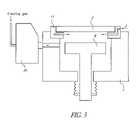
- FIG. 3is a schematic diagram showing a UV irradiation chamber where a remote plasma unit is attached usable in an embodiment of the present invention.
- FIG. 4is a schematic diagram showing a UV irradiation chamber usable in an embodiment of the present invention.
- FIG. 5is a graph showing relationships between UV transmission factor (%) and wavelength (nm) in examples.
- the present inventionprovides a method of cleaning a UV irradiation chamber comprising steps of: (i) after completion of irradiating a substrate with UV light transmitted through an optical transmitted window provided in the UV irradiation chamber, generating radical species of a cleaning gas outside the UV irradiation chamber; and (ii) introducing the radical species from the outside of the UV irradiation chamber into the UV irradiation chamber, thereby cleaning the optical transmitted window.
- the UV irradiation processcan be any suitable processes including those disclosed in U.S. Pat. No. 6,759,098 and U.S. Pat. No. 6,296,909, the disclosure of which is incorporated herein by reference in their entirety.
- the processmay comprise processing a substrate (e.g., a semiconductor substrate) placed on a susceptor provided in a UV irradiation chamber, by irradiating the substrate with UV light through an optical transmitted window provided in the UV chamber between a UV light source and the susceptor.
- a film constituted by Si, C, H, O, and optionally Ncan be formed on the substrate by e.g., PECVD, PEALD, PVD, etc.
- the UV irradiation processis a curing process of the film.
- the UV irradiation processneed not be limited to the curing process, and in an embodiment, the UV irradiation process is a light-CVD process.
- the filmincludes, but is not limited to, a low dielectric film or a silicon carboxide film.
- a significant amount of outgasis generated from the film as a result of decomposition of the chemical structures in the UV irradiation chamber.
- the outgasmay be composed of hydrocarbon species.
- the outgasaccumulates on a surface of the inner wall of the UV irradiation chamber including the optical transmitted window. The deposit of the accumulated outgas interferes with UV light transmission through the optical transmitted window, thereby decreasing efficiency of curing. Thus, particularly, the optical transmitted window needs to be cleaned frequently.
- radical species of a cleaning gasis generated by a method other than UV irradiation outside the UV irradiation chamber.
- UV irradiationradical species of a cleaning gas can be generated, but it is difficult to obtain a sufficient amount of radical species, although it depends on the wavelength of light and the intensity of light.
- a high-pressure mercury lampmay generate ozone from oxygen on the order of several to several tens ppm.
- An Xe excimer lasermay convert several percents of oxygen to ozone.
- the radical speciesare generated in a remote plasma unit. If the cleaning gas is oxygen, an ozonizer or ozone generator may be used in place of the remote plasma unit. The externally excited species have higher energy and can more efficiently clean the optical transmitted window than the conventional UV irradiation.
- the radical speciesare introduced from the outside of the UV irradiation chamber into the UV irradiation chamber, thereby cleaning the optical transmitted window.
- the cleaning gasmay be an oxygen gas.
- as high percent of oxygen as about 80%can be converted to ozone.
- a life of ozonemay be short and some of the radicals may not be maintained until the radicals reach the UV irradiation chamber.
- the radical speciesare further excited by irradiating the radical species with the UV light through the optical transmitted window.
- the cleaning processcan be controlled.
- the pressuremay be 10 Torr or less (e.g., 1-7 Torr)
- a flow rate of oxygen gasmay be 0.1-10 slm (e.g., 0.3-1 slm)
- a flow rate of inert gassuch as Ar, He, Kr, or Xe may be 0.5-15 slm (e.g., 1-5 slm; greater than that of oxygen gas)
- a cleaning timemay be 5-1000 sec (e.g., 10-600 sec, 50-200 sec).
- UV irradiationis combined where UV light has an intensity of 1 mW/cm2-500 mW/cm2 (e.g., 100 mW/cm2-400 mW/cm2) and a wavelength of 100-1000 nm (e.g., 200-400 nm).
- the cleaning gasmay be a gas containing fluorine in a molecule such as NF 3 , C2F6, and C3F8.
- the gas containing fluorinehas high energy and can efficiently clean the optical transmitted window.
- the gas containing fluorinemay damage the optical transmitted window by corroding its surface.
- the optical transmitted windowis made of synthetic glass (silicon oxide), and the synthetic glass is apt to be etched by fluorine-containing gas.
- the optical transmitted windowmay be constituted by a material which is resistant to fluorine-containing gas.
- the optical transmitted windowmay be constituted by a crystal of CaF 2 , MgF 2 , BaF 2 , or Al 2 O 3 .
- the optical transmitted windowmay be constituted by a synthetic quartz coated with CaF 2 , MgF 2 , BaF 2 , or Al 2 O 3 .
- CaF 2for example, has a higher optical transmission factor than SiO 2 and thus is preferred.
- the cleaning conditionsmay as follows:
- the pressuremay be 10 Torr or less (e.g., 1-7 Torr)
- a flow rate of fluorine-containing gase.g., NF 3
- a flow rate of inert gassuch as Ar, He, Kr, or Xe
- a cleaning timemay be 5-1000 sec (e.g., 10-600 sec, 50-200 sec).
- cleaning gasoxygen gas and fluorine-containing gas can be used in combination.
- the optical transmitted windowmay have a diameter of 110% to 150% of that of a substrate (e.g., 120% to 130%) (e.g., 360 mm to 380 mm for a substrate having a diameter of 300 mm), and have a thickness of 10 mm to 30 mm (e.g., about 20 mm) which is sufficient to be used in a vacuum.
- a distance between the optical transmitted window and the substratemay be 5 mm to 30 mm (e.g., 10 mm to 20 mm).
- the present inventionprovides a method of semiconductor-processing by UV irradiation and cleaning a UV irradiation chamber for semiconductor-processing, comprising the steps of: (i) processing a semiconductor substrate placed on a susceptor provided in a UV irradiation chamber, by irradiating the substrate with UV light through an optical transmitted window provided in the UV chamber between a UV light source and the susceptor; and (ii) after completion of the processing step, introducing radical species of a cleaning gas from the outside of the UV irradiation chamber into a space defined between the optical transmitted window and the susceptor, thereby cleaning the optical transmitted window.
- the UV lightmay have a wavelength of 200 nm to 500 nm (e.g., 100 nm to 400 nm).
- FIG. 1is a schematic diagram showing a UV irradiation apparatus useable in an embodiment of the present invention.
- This apparatuscomprises a chamber that can be controlled to a range of pressure conditions from vacuum to near atmospheric pressure, and a UV irradiation unit installed above the chamber.
- this apparatuscomprises a UV lamp 4 , an irradiation window 2 , a gas introduction port 3 , a UV irradiation chamber 1 , a heater table 8 , an exhaust port 5 connected to a vacuum pump, and a load lock chamber 7 having a LL arm 6 and connected to the UV irradiation chamber.
- the apparatusneed not conform to this figure as long as UV irradiation can be implemented.
- This UV irradiation apparatushas the UV emitter 4 that emits UV light continuously or in pulses, the heater 8 installed in parallel with and facing the aforementioned emitter, and the irradiation window glass 2 installed in parallel with and facing the UV emitter 4 and heater 8 at a position between the two.
- the irradiation window 2is used to achieve uniform UV irradiation by shielding the reactor from atmosphere while transmitting UV light.
- the UV emitter 4 in the UV irradiation unitmultiple tubular emitters may be placed in parallel with one another, with the layout of these emitters arranged properly so as to achieve uniform illuminance, as shown in FIG. 1 .
- a reflector 9is provided to cause the UV light from each UV emitter to properly reflect onto the thin film (the reflector resembles an umbrella placed over the UV lamp), and the angle of the reflector 9 is made adjustable to achieve uniform illuminance.
- this apparatushas a flange 11 in which the irradiation window glass 2 is set, so as to separate the substrate processing part in the chamber 1 that can be controlled to a range of pressure conditions from vacuum to near atmospheric pressure, from the UV emission part that stores the UV emitters 4 emitting UV light continuously or in pulses.
- This flange 11is connected to the gas introduction port 3 and multiple gas discharge ports are provided in circumferential direction at specified intervals so that gas is discharged uniformly from points along the circumference toward the interior.
- gasis introduced through the flange 11 and the multiple gas introduction ports are arranged symmetrically to create a uniform processing ambience.
- the UV emitter 4is structured in such a way that it can be easily removed and replaced.
- the pressure in the substrate processing partis adjusted by a pressure control valve 21 provided at the exhaust port 5 .
- the UV Osion partis also a sealed space, it has an introduction port and discharge port (not illustrated) for purge gas (constantly purged by atmosphere, N 2 , etc.).
- a gas selected from Ar, CO, CO 2 , C 2 H 4 , CH 4 , H 2 , He, Kr, Ne, N 2 , O 2 , Xe, alcohol gases and organic gasesis introduced to the chamber 1 to create an ambience with a pressure between approx. 0.1 Torr and near atmosphere (including 1 Torr, 10 Torr, 50 Torr, 100 Torr, 1,000 Torr and any values between the foregoing numbers), and next a semiconductor substrate, which is the processing target, is transferred from the load lock chamber 7 via the gate valve and placed on the heater 8 that has been set to a temperature between approx. 0° C.
- UV light with a wavelength between approx. 100 nm and approx. 400 nmincluding 150 nm, 200 nm, 250 nm, 300 nm, 350 nm and any values between the foregoing numbers, but preferably approx. 200 nm
- outputbetween 1 mW/cm 2 and approx.
- 1,000 mW/cm 2(including 10 mW/cm 2 , 50 mW/cm 2 , 100 mW/cm 2 , 200 mW/cm 2 , 500 mW/cm 2 , 800 mW/cm 2 and any values between the foregoing numbers) is irradiated at an appropriate distance (gap) (between 1 cm and 100 cm) from the UV emitters 4 , onto the thin film on the semiconductor substrate either continuously or in pulses at a frequency between approx. 1 Hz and approx. 1,000 Hz (including 10 Hz, 100 Hz, 200 Hz, 500 Hz and any values between the foregoing numbers).
- the irradiation timeis between approx. 1 sec and approx. 20 min (including 5 sec, 10 sec, 20 sec, 50 sec, 100 sec, 200 sec, 500 sec, 1,000 sec and any values between the foregoing numbers).
- the gas in the chamber 1is discharged from the exhaust port 5 .
- This semiconductor manufacturing apparatuscarries out the above series of processing steps according to an automatic sequence, where the processing steps implemented include introduction of gas, irradiation of UV light, stopping of irradiation, and stopping of gas.
- FIG. 3shows a schematic diagram of a condition where a remote plasma unit 31 is connected to the UV chamber 1 . Cleaning gas is introduced to the remote plasma unit 31 , where it is excited and subsequently introduced to the UV chamber 1 .
- NF 3can be used as the cleaning gas in an embodiment of the present invention.
- NF 3is introduced to the remote plasma unit (refer to FIG. 3 ) where it is broken down to generate fluorine radicals, after which the generated fluorine radicals are introduced to the chamber to break down and remove the contaminants on the irradiation window and interior chamber walls.
- FIG. 5shows the result of measurement using a spectrophotometer, showing how much of light of which wavelength is transmitted by the irradiation window glass (thickness: 20 mm). Measurement was performed with a synthetic quartz (SiO 2 ) glass and a CaF 2 glass. In FIG. 5 , first the UV transmission factor (%) of the irradiation glass was measured, and then a substrate (300 mm) on which a low-k film (SiCOH film) had been formed was transferred into the UV chamber and cured under the following conditions:
- the UV transmission factor (%) of the irradiation window glasswas measured again. (Was UV irradiation performed only once or multiple times?)
- the cleaning conditionswere as follows:
- Remote plasma unitASTRONTM, Cleaning gas: NF 3 , Chamber pressure: 1 to 10 Torr, Flow rate of cleaning gas: 0.5 to 2 slm, Flow rate of Ar gas: 2 to 5 slm, Cleaning time: 1 min.
- the UV transmission factor (%) of the irradiation window glasswas measured again.
- the experiment carried out using a CaF 2 glass window in a manner similar to the SiO 2 experimentrevealed that, when the irradiation window was made of CaF 2 resistant to fluorine, fluorine erosion was prevented and the effect of radical cleaning using NF 3 improved, as shown in FIG. 5 .
- CaF 2was used in light of its resistance to fluorine.
- CaF 2is also favored in that its overall transmission factor is higher than that of SiO 2 .
- the transmission factorwas between 92% and 94% in the initial condition, which then dropped by approx. 1% after the curing of the low-k film.
- the cleaning speed of the UV chambercan be increased dramatically by cleaning the UV irradiation window using a remote plasma unit, or by using an irradiation window resistant to fluorine and then cleaning the window using a fluorine cleaning gas offering high cleaning performance.
Landscapes
- Chemical & Material Sciences (AREA)
- Materials Engineering (AREA)
- General Chemical & Material Sciences (AREA)
- Chemical Kinetics & Catalysis (AREA)
- Engineering & Computer Science (AREA)
- Mechanical Engineering (AREA)
- Metallurgy (AREA)
- Organic Chemistry (AREA)
- Toxicology (AREA)
- Health & Medical Sciences (AREA)
- Physics & Mathematics (AREA)
- Optics & Photonics (AREA)
- Drying Of Semiconductors (AREA)
- Cleaning Or Drying Semiconductors (AREA)
Abstract
Description
- This application claims the benefit of U.S. Provisional Application No. 60/845,732, filed Sep. 19, 2006, the disclosure of which is herein incorporated by reference in its entirety.
- 1. Field of the Invention
- The present invention generally relates to semiconductor-processing by ultraviolet (UV) radiation and cleaning of a ultraviolet (UV) radiation chamber for semiconductor-processing, particularly cleaning of an optical transmitted window provided in a UV irradiation chamber.
- 2. Description of the Related Art
- Traditionally, UV processing apparatuses have been used in general in the property modification of various processing targets by means of UV light as well as in the production of substances that utilize photochemical reaction. With the trend for higher integration of devices in recent years, wiring designs are becoming finer and multi-layer wiring structures are being adopted, which in turn is making it necessary to reduce inter-layer volumes in devices to achieve higher processing speeds and lower power consumptions. Low-k (low dielectric constant film) materials are used to reduce inter-layer volumes in devices. As the dielectric constant drops, however, mechanical strength (elastic modulus, or EM) also drops and the low-k material thus becomes less resistant to stress received in the subsequent processes such as CMP, wire bonding and packaging. One method to address the aforementioned problem is to cure the low-k material through UV irradiation to improve its mechanical strength (refer to U.S. Pat. No. 6,759,098 and U.S. Pat. No. 6,296,909 for examples). UV irradiation causes the low-k material to contract and harden, resulting in an improvement of mechanical strength by 50 to 200%.
- Another requirement resulting from the recent trend of high-integration devices is to obtain various thin films using thermal CVD or PECVD in a condition free from heat or plasma damage. To meet this requirement, photo-CVD that utilizes photochemical reaction has been studied.
- However, irradiating optical energy onto the processing target or reaction space by any of the aforementioned methods requires the UV lamp to be separated from the reaction space because: (1) the pressure in the reaction space must be controlled along with the ambient gas, (2) the generated gas can contaminate the UV lamp, and (3) the generated gas must be discharged safely. As a division plate used for this purpose, normally optical transmitted window made of synthetic quartz, a material that transmits optical energy, has been traditionally employed.
- However, UV light that generates high energy tends to cause a drop in transmission factor depending on the material of the transmitted window and also due to deposits accumulating on the window material, and therefore the maintenance cycle (number of processings and processing time required before the transmitted window is cleaned or replaced) must be set very short in the cure process where a large amount of outgas (cracked gas generated by the irradiated film) generates.
- Traditionally, the method of introducing O2to the reaction space and irradiating UV to generate ozone, thereby removing the deposits by means of the generated ozone, has been used in general. However, other methods offering higher efficiency are being sought in light of the longer cleaning time required in the cure process where a large amount of outgas generates.
- In an embodiment of the present invention, O2is activated by a remote plasma unit or ozone generator and then the activated O2is introduced to the chamber to implement cleaning. In an embodiment, the aforementioned activated oxygen is irradiated with a UV lamp to accelerate activation for effective cleaning. In an embodiment, either of the aforementioned cleaning methods may be combined with the traditional ozone cleaning method using O2and UV light.
- In another embodiment of the present invention, a more efficient cleaning method is implemented whereby, instead of O2used in the aforementioned methods or as an additive gas, a cleaning gas containing fluorine is activated by a remote plasma unit and then introduced into the chamber. In this case, in an embodiment a material offering a high transmission factor is selected for the transmitted window to prevent the window from corroding as a result of fluorine. Examples of such material include a crystal of CaF2, MgF2, BaF2or Al2O3, or a synthetic quartz coated with CaF2, MgF2, BaF2or Al2O3.
- For purposes of summarizing the invention and the advantages achieved over the related art, certain objects and advantages of the invention are described in this disclosure. Of course, it is to be understood that not necessarily all such objects or advantages may be achieved in accordance with any particular embodiment of the invention. Thus, for example, those skilled in the art will recognize that the invention may be embodied or carried out in a manner that achieves or optimizes one advantage or group of advantages as taught herein without necessarily achieving other objects or advantages as may be taught or suggested herein.
- Further aspects, features and advantages of this invention will become apparent from the detailed description of the preferred embodiments which follow.
- These and other features of this invention will now be described with reference to the drawings of preferred embodiments which are intended to illustrate and not to limit the invention. The drawings are oversimplified for illustrative purposes and not to scale.
FIG. 1 is a schematic diagram showing a UV irradiation apparatus useable in an embodiment of the present invention.FIG. 2( a) is a schematic diagram showing a UV irradiation chamber usable in an embodiment of the present invention.FIG. 2( b) is a schematic diagram showing a top view of the UV irradiation chamber shown inFIG. 2( a).FIG. 3 is a schematic diagram showing a UV irradiation chamber where a remote plasma unit is attached usable in an embodiment of the present invention.FIG. 4 is a schematic diagram showing a UV irradiation chamber usable in an embodiment of the present invention.FIG. 5 is a graph showing relationships between UV transmission factor (%) and wavelength (nm) in examples.- The invention will be explained further with reference to specific embodiments, but the specific embodiments are not intended to limit the present invention.
- In an embodiment, the present invention provides a method of cleaning a UV irradiation chamber comprising steps of: (i) after completion of irradiating a substrate with UV light transmitted through an optical transmitted window provided in the UV irradiation chamber, generating radical species of a cleaning gas outside the UV irradiation chamber; and (ii) introducing the radical species from the outside of the UV irradiation chamber into the UV irradiation chamber, thereby cleaning the optical transmitted window.
- The UV irradiation process can be any suitable processes including those disclosed in U.S. Pat. No. 6,759,098 and U.S. Pat. No. 6,296,909, the disclosure of which is incorporated herein by reference in their entirety. Typically, the process may comprise processing a substrate (e.g., a semiconductor substrate) placed on a susceptor provided in a UV irradiation chamber, by irradiating the substrate with UV light through an optical transmitted window provided in the UV chamber between a UV light source and the susceptor.
- In an embodiment, prior to the UV irradiation process, a film constituted by Si, C, H, O, and optionally N can be formed on the substrate by e.g., PECVD, PEALD, PVD, etc. In the above, the UV irradiation process is a curing process of the film. The UV irradiation process need not be limited to the curing process, and in an embodiment, the UV irradiation process is a light-CVD process.
- The film includes, but is not limited to, a low dielectric film or a silicon carboxide film. When the film formed on the substrate is cured in the UV irradiation chamber, a significant amount of outgas is generated from the film as a result of decomposition of the chemical structures in the UV irradiation chamber. The outgas may be composed of hydrocarbon species. The outgas accumulates on a surface of the inner wall of the UV irradiation chamber including the optical transmitted window. The deposit of the accumulated outgas interferes with UV light transmission through the optical transmitted window, thereby decreasing efficiency of curing. Thus, particularly, the optical transmitted window needs to be cleaned frequently.
- In an embodiment, radical species of a cleaning gas is generated by a method other than UV irradiation outside the UV irradiation chamber. By UV irradiation, radical species of a cleaning gas can be generated, but it is difficult to obtain a sufficient amount of radical species, although it depends on the wavelength of light and the intensity of light. For example, a high-pressure mercury lamp may generate ozone from oxygen on the order of several to several tens ppm. An Xe excimer laser may convert several percents of oxygen to ozone. In an embodiment, the radical species are generated in a remote plasma unit. If the cleaning gas is oxygen, an ozonizer or ozone generator may be used in place of the remote plasma unit. The externally excited species have higher energy and can more efficiently clean the optical transmitted window than the conventional UV irradiation.
- In an embodiment, the radical species are introduced from the outside of the UV irradiation chamber into the UV irradiation chamber, thereby cleaning the optical transmitted window. The cleaning gas may be an oxygen gas. In an embodiment, by a remote plasma unit, as high percent of oxygen as about 80% can be converted to ozone. However, a life of ozone may be short and some of the radicals may not be maintained until the radicals reach the UV irradiation chamber. Thus, in a preferred embodiment, the radical species are further excited by irradiating the radical species with the UV light through the optical transmitted window.
- When a remote plasma unit (e.g., ASTRON™ manufactured by MKS) is used for exciting an oxygen gas, by controlling the pressure and flow in the UV irradiation chamber, the cleaning process can be controlled. In an embodiment, the pressure may be 10 Torr or less (e.g., 1-7 Torr), a flow rate of oxygen gas may be 0.1-10 slm (e.g., 0.3-1 slm), a flow rate of inert gas such as Ar, He, Kr, or Xe may be 0.5-15 slm (e.g., 1-5 slm; greater than that of oxygen gas), and a cleaning time may be 5-1000 sec (e.g., 10-600 sec, 50-200 sec). Preferably, in the above, UV irradiation is combined where UV light has an intensity of 1 mW/cm2-500 mW/cm2 (e.g., 100 mW/cm2-400 mW/cm2) and a wavelength of 100-1000 nm (e.g., 200-400 nm).
- In an embodiment, the cleaning gas may be a gas containing fluorine in a molecule such as NF3, C2F6, and C3F8. The gas containing fluorine has high energy and can efficiently clean the optical transmitted window. However, on the other hand, the gas containing fluorine may damage the optical transmitted window by corroding its surface. Normally, the optical transmitted window is made of synthetic glass (silicon oxide), and the synthetic glass is apt to be etched by fluorine-containing gas. In a preferred embodiment, the optical transmitted window may be constituted by a material which is resistant to fluorine-containing gas. In an embodiment, the optical transmitted window may be constituted by a crystal of CaF2, MgF2, BaF2, or Al2O3. In another embodiment, the optical transmitted window may be constituted by a synthetic quartz coated with CaF2, MgF2, BaF2, or Al2O3. CaF2, for example, has a higher optical transmission factor than SiO2and thus is preferred.
- When a fluorine-containing gas is used as the cleaning gas, although additional UV irradiation can be performed but need not be performed in the UV irradiation chamber in an embodiment. In an embodiment, the cleaning conditions may as follows: The pressure may be 10 Torr or less (e.g., 1-7 Torr), a flow rate of fluorine-containing gas (e.g., NF3) may be 0.1-5 slm (e.g., 0.5-1.5 slm), a flow rate of inert gas such as Ar, He, Kr, or Xe may be 1-15 slm (e.g., 1-5 slmgreater than that of fluorine-containing gas), and a cleaning time may be 5-1000 sec (e.g., 10-600 sec, 50-200 sec).
- In the above, as the cleaning gas, oxygen gas and fluorine-containing gas can be used in combination.
- In an embodiment, the optical transmitted window may have a diameter of 110% to 150% of that of a substrate (e.g., 120% to 130%) (e.g., 360 mm to 380 mm for a substrate having a diameter of 300 mm), and have a thickness of 10 mm to 30 mm (e.g., about 20 mm) which is sufficient to be used in a vacuum. In an embodiment, a distance between the optical transmitted window and the substrate may be 5 mm to 30 mm (e.g., 10 mm to 20 mm).
- In an embodiment, the present invention provides a method of semiconductor-processing by UV irradiation and cleaning a UV irradiation chamber for semiconductor-processing, comprising the steps of: (i) processing a semiconductor substrate placed on a susceptor provided in a UV irradiation chamber, by irradiating the substrate with UV light through an optical transmitted window provided in the UV chamber between a UV light source and the susceptor; and (ii) after completion of the processing step, introducing radical species of a cleaning gas from the outside of the UV irradiation chamber into a space defined between the optical transmitted window and the susceptor, thereby cleaning the optical transmitted window. In the processing step, the UV light may have a wavelength of 200 nm to 500 nm (e.g., 100 nm to 400 nm).
- The present invention will be explained with reference to drawings and preferred embodiments which are not intended to limit the present invention.
- In the present disclosure where conditions and/or structures are not specified, the skilled artisan in the art can readily provide such conditions and/or structures, in view of the present disclosure, as a matter of routine experimentation.
FIG. 1 is a schematic diagram showing a UV irradiation apparatus useable in an embodiment of the present invention. This apparatus comprises a chamber that can be controlled to a range of pressure conditions from vacuum to near atmospheric pressure, and a UV irradiation unit installed above the chamber. To be specific, this apparatus comprises a UV lamp4, anirradiation window 2, agas introduction port 3, aUV irradiation chamber 1, a heater table8, anexhaust port 5 connected to a vacuum pump, and a load lock chamber7 having a LL arm6 and connected to the UV irradiation chamber. It should be noted, however, that the apparatus need not conform to this figure as long as UV irradiation can be implemented.- This UV irradiation apparatus has the UV emitter4 that emits UV light continuously or in pulses, the
heater 8 installed in parallel with and facing the aforementioned emitter, and theirradiation window glass 2 installed in parallel with and facing the UV emitter4 andheater 8 at a position between the two. Theirradiation window 2 is used to achieve uniform UV irradiation by shielding the reactor from atmosphere while transmitting UV light. As for the UV emitter4 in the UV irradiation unit, multiple tubular emitters may be placed in parallel with one another, with the layout of these emitters arranged properly so as to achieve uniform illuminance, as shown inFIG. 1 . Areflector 9 is provided to cause the UV light from each UV emitter to properly reflect onto the thin film (the reflector resembles an umbrella placed over the UV lamp), and the angle of thereflector 9 is made adjustable to achieve uniform illuminance. - As shown in the schematic diagrams in
FIGS. 2( a) and2(b), this apparatus has aflange 11 in which theirradiation window glass 2 is set, so as to separate the substrate processing part in thechamber 1 that can be controlled to a range of pressure conditions from vacuum to near atmospheric pressure, from the UV emission part that stores the UV emitters4 emitting UV light continuously or in pulses. Thisflange 11 is connected to thegas introduction port 3 and multiple gas discharge ports are provided in circumferential direction at specified intervals so that gas is discharged uniformly from points along the circumference toward the interior. To be specific, gas is introduced through theflange 11 and the multiple gas introduction ports are arranged symmetrically to create a uniform processing ambience. The UV emitter4 is structured in such a way that it can be easily removed and replaced. - As shown in the schematic diagram in
FIG. 4 , the pressure in the substrate processing part is adjusted by apressure control valve 21 provided at theexhaust port 5. While the UV Osion part is also a sealed space, it has an introduction port and discharge port (not illustrated) for purge gas (constantly purged by atmosphere, N2, etc.). - Examples of the UV irradiation process are shown below. It should be noted, however, that the present invention is not at all limited to these embodiments. First, a gas selected from Ar, CO, CO2, C2H4, CH4, H2, He, Kr, Ne, N2, O2, Xe, alcohol gases and organic gases is introduced to the
chamber 1 to create an ambience with a pressure between approx. 0.1 Torr and near atmosphere (including 1 Torr, 10 Torr, 50 Torr, 100 Torr, 1,000 Torr and any values between the foregoing numbers), and next a semiconductor substrate, which is the processing target, is transferred from the load lock chamber7 via the gate valve and placed on theheater 8 that has been set to a temperature between approx. 0° C. and approx. 650° C. (including 10° C., 500° C., 100° C., 200° C., 300° C., 400° C., 500° C., 600° C. and any values between the foregoing numbers, but preferably between 300° C. and 450° C.), after which UV light with a wavelength between approx. 100 nm and approx. 400 nm (including 150 nm, 200 nm, 250 nm, 300 nm, 350 nm and any values between the foregoing numbers, but preferably approx. 200 nm) and output between 1 mW/cm2and approx. 1,000 mW/cm2(including 10 mW/cm2, 50 mW/cm2, 100 mW/cm2, 200 mW/cm2, 500 mW/cm2, 800 mW/cm2and any values between the foregoing numbers) is irradiated at an appropriate distance (gap) (between 1 cm and 100 cm) from the UV emitters4, onto the thin film on the semiconductor substrate either continuously or in pulses at a frequency between approx. 1 Hz and approx. 1,000 Hz (including 10 Hz, 100 Hz, 200 Hz, 500 Hz and any values between the foregoing numbers). The irradiation time is between approx. 1 sec and approx. 20 min (including 5 sec, 10 sec, 20 sec, 50 sec, 100 sec, 200 sec, 500 sec, 1,000 sec and any values between the foregoing numbers). The gas in thechamber 1 is discharged from theexhaust port 5. - This semiconductor manufacturing apparatus carries out the above series of processing steps according to an automatic sequence, where the processing steps implemented include introduction of gas, irradiation of UV light, stopping of irradiation, and stopping of gas.
- When outgas is generated from the thin film on the semiconductor substrate as a result of UV irradiation, substances constituting the outgas deposit on the irradiation window glass made of synthetic quartz or the like, and also on the interior walls of the chamber. The contaminants deposited on the irradiation window absorb UV light and decrease the cure efficiency. The contaminants deposited on the interior walls of the chamber can produce particles as they are separated from the walls.
- Cleaning is performed to remove these contaminants. For example, cleaning is implemented by causing ozonization of O2using UV light and removing the contaminants by causing them to react with ozone. Since the percentage of O2ozonized by UV light is very low, in an embodiment of the present invention O2is converted to radicals using a remote plasma unit before being introduced to the chamber, and the resulting O2radicals are then ozonized by UV light to increase the ozone production efficiency.
FIG. 3 shows a schematic diagram of a condition where aremote plasma unit 31 is connected to theUV chamber 1. Cleaning gas is introduced to theremote plasma unit 31, where it is excited and subsequently introduced to theUV chamber 1. - On the other hand, in cases where using ozone alone may not achieve sufficient cleaning when the film to be cured generates deposits that cannot be broken down by ozone or a large amount of deposits, NF3can be used as the cleaning gas in an embodiment of the present invention. To be specific, NF3is introduced to the remote plasma unit (refer to
FIG. 3 ) where it is broken down to generate fluorine radicals, after which the generated fluorine radicals are introduced to the chamber to break down and remove the contaminants on the irradiation window and interior chamber walls. - However, these fluorine radicals, although having the effect of breaking down and removing the contaminants in the reactor, also cause the adverse effect of eroding the surface of the irradiation window made of synthetic quartz and thereby reducing the UV transmission factor.
FIG. 5 shows the result of measurement using a spectrophotometer, showing how much of light of which wavelength is transmitted by the irradiation window glass (thickness: 20 mm). Measurement was performed with a synthetic quartz (SiO2) glass and a CaF2glass. InFIG. 5 , first the UV transmission factor (%) of the irradiation glass was measured, and then a substrate (300 mm) on which a low-k film (SiCOH film) had been formed was transferred into the UV chamber and cured under the following conditions:- Pressure: 1 to 100 Torr, Introduced gas: N2, Temperature: 300 to 450° C., Distance between substrate and irradiation window: 0.1 to 10 cm, UV wavelength: 100 to 400 nm, Output: 5 to 400 mW/cm2, Irradiation time: 60 to 600 sec.
- After the low-k film was cured by UV light under the above conditions, the UV transmission factor (%) of the irradiation window glass was measured again. (Was UV irradiation performed only once or multiple times?)
- Next, the interior of the UV chamber was cleaned. The cleaning conditions were as follows:
- Remote plasma unit: ASTRON™, Cleaning gas: NF3, Chamber pressure: 1 to 10 Torr, Flow rate of cleaning gas: 0.5 to 2 slm, Flow rate of Ar gas: 2 to 5 slm, Cleaning time: 1 min.
- After the cleaning, the UV transmission factor (%) of the irradiation window glass was measured again.
- As a result, it was found that, although synthetic quartz (SiO2) transmitted 90% or more of UV light with a wavelength of 200 nm or more in the initial condition, once the low-k film was cured by UV light the transmission factor dropped by approx. 1 to 2% for light with a wavelength of 300 nm or less, as shown in
FIG. 5 . After NF3cleaning was carried out for 1 minute using the remote plasma unit, the transmission factor dropped considerably and the extent of drop was as much as 10% with light with a wavelength of 200 nm. Whitening and roughening of the glass surface was also visually observed. - On the other hand, the experiment carried out using a CaF2glass window in a manner similar to the SiO2experiment revealed that, when the irradiation window was made of CaF2resistant to fluorine, fluorine erosion was prevented and the effect of radical cleaning using NF3improved, as shown in
FIG. 5 . In this experiment, CaF2was used in light of its resistance to fluorine. CaF2is also favored in that its overall transmission factor is higher than that of SiO2. To be specific, the transmission factor was between 92% and 94% in the initial condition, which then dropped by approx. 1% after the curing of the low-k film. After1 minute of NF3cleaning using the remote plasma unit, however, the transmission factor recovered to the initial level (although the transmission factor measured after the cleaning was higher than the level in the initial condition, this is probably due to a measurement error or caused by the removal, by the cleaning, of contaminants that were already deposited in the initial condition). No whitening or roughening was visually observed. This confirms sufficient fluorine resistance of the CaF2glass. - As explained above, in an embodiment of the present invention the cleaning speed of the UV chamber can be increased dramatically by cleaning the UV irradiation window using a remote plasma unit, or by using an irradiation window resistant to fluorine and then cleaning the window using a fluorine cleaning gas offering high cleaning performance.
- It will be understood by those of skill in the art that numerous and various modifications can be made without departing from the spirit of the present invention. Therefore, it should be clearly understood that the forms of the present invention are illustrative only and are not intended to limit the scope of the present invention.
Claims (16)
1. A method of cleaning a UV irradiation chamber comprising steps of:
after completion of irradiating a substrate with UV light transmitted through an optical transmitted window provided in the UV irradiation chamber, generating radical species of a cleaning gas outside the UV irradiation chamber; and
introducing the radical species from the outside of the UV irradiation chamber into the UV irradiation chamber, thereby cleaning the optical transmitted window.
2. The method according toclaim 1 , wherein the cleaning gas is an oxygen gas.
3. The method according toclaim 2 , further comprising further exciting the radical species by irradiating the radical species with the UV light through the optical transmitted window.
4. The method according toclaim 1 , wherein the cleaning gas is a gas containing fluorine in a molecule.
5. The method according toclaim 4 , wherein the optical transmitted window is constituted by a crystal of CaF2, MgF2, BaF2, or Al2O3.
6. The method according toclaim 4 , wherein the optical transmitted window is constituted by a synthetic quartz coated with CaF2, MgF2, BaF2, or Al2O3.
7. The method according toclaim 1 , wherein the generation step comprises generating the radical species by a method other than UV irradiation.
8. The method according toclaim 7 , wherein the generation step comprises generating the radical species in a remote plasma unit.
9. A method of semiconductor-processing by UV irradiation and cleaning a UV irradiation chamber for semiconductor-processing, comprising the steps of:
processing a semiconductor substrate placed on a susceptor provided in a UV irradiation chamber, by irradiating the substrate with UV light through an optical transmitted window provided in the UV chamber between a UV light source and the susceptor; and
after completion of the processing step, introducing radical species of a cleaning gas from the outside of the UV irradiation chamber into a space defined between the optical transmitted window and the susceptor, thereby cleaning the optical transmitted window.
10. The method according toclaim 9 , wherein the UV light has a wavelength of 200 nm to 500 nm.
11. The method according toclaim 9 , wherein in the processing step, a low dielectric film or a silicon carboxide film is formed on the substrate.
12. The method according toclaim 9 , wherein the cleaning gas is an oxygen gas.
13. The method according toclaim 12 , further comprising further exciting the radical species by irradiating the radical species with the UV light through the optical transmitted window.
14. The method according toclaim 9 , wherein the cleaning gas is a gas containing fluorine in a molecule.
15. The method according toclaim 14 , wherein in the processing step, the substrate is irradiated through the optical transmitted window constituted by a crystal of CaF2, MgF2, BaF2, or Al2O3.
16. The method according toclaim 14 , wherein in the processing step, the substrate is irradiated through the optical transmitted window constituted by a synthetic quartz coated with CaF2, MgF2, BaF2, or Al2O3.
Priority Applications (1)
| Application Number | Priority Date | Filing Date | Title |
|---|---|---|---|
| US11/857,639US7789965B2 (en) | 2006-09-19 | 2007-09-19 | Method of cleaning UV irradiation chamber |
Applications Claiming Priority (2)
| Application Number | Priority Date | Filing Date | Title |
|---|---|---|---|
| US84573206P | 2006-09-19 | 2006-09-19 | |
| US11/857,639US7789965B2 (en) | 2006-09-19 | 2007-09-19 | Method of cleaning UV irradiation chamber |
Publications (2)
| Publication Number | Publication Date |
|---|---|
| US20080066778A1true US20080066778A1 (en) | 2008-03-20 |
| US7789965B2 US7789965B2 (en) | 2010-09-07 |
Family
ID=39187294
Family Applications (1)
| Application Number | Title | Priority Date | Filing Date |
|---|---|---|---|
| US11/857,639Active2028-08-04US7789965B2 (en) | 2006-09-19 | 2007-09-19 | Method of cleaning UV irradiation chamber |
Country Status (1)
| Country | Link |
|---|---|
| US (1) | US7789965B2 (en) |
Cited By (405)
| Publication number | Priority date | Publication date | Assignee | Title |
|---|---|---|---|---|
| US20080093709A1 (en)* | 2006-10-20 | 2008-04-24 | Renesas Technology Corp. | Manufacturing method of semiconductor device and semiconductor device |
| WO2009146744A1 (en)* | 2008-06-05 | 2009-12-10 | Osram Gesellschaft mit beschränkter Haftung | Method for treating surfaces, lamp for said method, and irradiation system having said lamp |
| US7789965B2 (en)* | 2006-09-19 | 2010-09-07 | Asm Japan K.K. | Method of cleaning UV irradiation chamber |
| US20110017231A1 (en)* | 2009-07-21 | 2011-01-27 | Mitake Tatsuhiro | Method of cleaning support plate |
| US20110097900A1 (en)* | 2009-10-28 | 2011-04-28 | Lam Research Corporation | Quartz window for a degas chamber |
| US20110159202A1 (en)* | 2009-12-29 | 2011-06-30 | Asm Japan K.K. | Method for Sealing Pores at Surface of Dielectric Layer by UV Light-Assisted CVD |
| US20110259862A1 (en)* | 2008-09-05 | 2011-10-27 | Mtt Technologies Limited | Additive Manufacturing Apparatus with a Chamber and a Removably-Mountable Optical Module; Method of Preparing a Laser Processing Apparatus with such Removably-Mountable Optical Module |
| WO2012054206A3 (en)* | 2010-10-19 | 2012-06-21 | Applied Materials, Inc. | Quartz showerhead for nanocure uv chamber |
| WO2012074816A3 (en)* | 2010-11-30 | 2012-10-04 | Applied Materials, Inc. | Method and apparatus for modulating wafer treatment profile in uv chamber |
| US8664627B1 (en)* | 2012-08-08 | 2014-03-04 | Asm Ip Holding B.V. | Method for supplying gas with flow rate gradient over substrate |
| US20140116335A1 (en)* | 2012-10-31 | 2014-05-01 | Asm Ip Holding B.V. | UV Irradiation Apparatus with Cleaning Mechanism and Method for Cleaning UV Irradiation Apparatus |
| CN104752264A (en)* | 2013-12-31 | 2015-07-01 | 北京北方微电子基地设备工艺研究中心有限责任公司 | Fixing structure of isolating window and cavity |
| JP2015529395A (en)* | 2012-08-23 | 2015-10-05 | アプライド マテリアルズ インコーポレイテッドApplied Materials,Incorporated | Method and hardware for cleaning a UV chamber |
| US9324811B2 (en) | 2012-09-26 | 2016-04-26 | Asm Ip Holding B.V. | Structures and devices including a tensile-stressed silicon arsenic layer and methods of forming same |
| US9384987B2 (en) | 2012-04-04 | 2016-07-05 | Asm Ip Holding B.V. | Metal oxide protective layer for a semiconductor device |
| US9394608B2 (en) | 2009-04-06 | 2016-07-19 | Asm America, Inc. | Semiconductor processing reactor and components thereof |
| US9404587B2 (en) | 2014-04-24 | 2016-08-02 | ASM IP Holding B.V | Lockout tagout for semiconductor vacuum valve |
| US9412564B2 (en) | 2013-07-22 | 2016-08-09 | Asm Ip Holding B.V. | Semiconductor reaction chamber with plasma capabilities |
| US9447498B2 (en) | 2014-03-18 | 2016-09-20 | Asm Ip Holding B.V. | Method for performing uniform processing in gas system-sharing multiple reaction chambers |
| US9455138B1 (en) | 2015-11-10 | 2016-09-27 | Asm Ip Holding B.V. | Method for forming dielectric film in trenches by PEALD using H-containing gas |
| US9478415B2 (en) | 2015-02-13 | 2016-10-25 | Asm Ip Holding B.V. | Method for forming film having low resistance and shallow junction depth |
| US9484191B2 (en) | 2013-03-08 | 2016-11-01 | Asm Ip Holding B.V. | Pulsed remote plasma method and system |
| US9543180B2 (en) | 2014-08-01 | 2017-01-10 | Asm Ip Holding B.V. | Apparatus and method for transporting wafers between wafer carrier and process tool under vacuum |
| US9556516B2 (en) | 2013-10-09 | 2017-01-31 | ASM IP Holding B.V | Method for forming Ti-containing film by PEALD using TDMAT or TDEAT |
| US9558931B2 (en) | 2012-07-27 | 2017-01-31 | Asm Ip Holding B.V. | System and method for gas-phase sulfur passivation of a semiconductor surface |
| US9589770B2 (en) | 2013-03-08 | 2017-03-07 | Asm Ip Holding B.V. | Method and systems for in-situ formation of intermediate reactive species |
| US9607837B1 (en) | 2015-12-21 | 2017-03-28 | Asm Ip Holding B.V. | Method for forming silicon oxide cap layer for solid state diffusion process |
| US9605342B2 (en) | 2012-09-12 | 2017-03-28 | Asm Ip Holding B.V. | Process gas management for an inductively-coupled plasma deposition reactor |
| US9627221B1 (en) | 2015-12-28 | 2017-04-18 | Asm Ip Holding B.V. | Continuous process incorporating atomic layer etching |
| US9640416B2 (en) | 2012-12-26 | 2017-05-02 | Asm Ip Holding B.V. | Single-and dual-chamber module-attachable wafer-handling chamber |
| US9647114B2 (en) | 2015-08-14 | 2017-05-09 | Asm Ip Holding B.V. | Methods of forming highly p-type doped germanium tin films and structures and devices including the films |
| US9657845B2 (en) | 2014-10-07 | 2017-05-23 | Asm Ip Holding B.V. | Variable conductance gas distribution apparatus and method |
| US9659799B2 (en) | 2012-08-28 | 2017-05-23 | Asm Ip Holding B.V. | Systems and methods for dynamic semiconductor process scheduling |
| US9711345B2 (en) | 2015-08-25 | 2017-07-18 | Asm Ip Holding B.V. | Method for forming aluminum nitride-based film by PEALD |
| US9735024B2 (en) | 2015-12-28 | 2017-08-15 | Asm Ip Holding B.V. | Method of atomic layer etching using functional group-containing fluorocarbon |
| US9754779B1 (en) | 2016-02-19 | 2017-09-05 | Asm Ip Holding B.V. | Method for forming silicon nitride film selectively on sidewalls or flat surfaces of trenches |
| US9793135B1 (en) | 2016-07-14 | 2017-10-17 | ASM IP Holding B.V | Method of cyclic dry etching using etchant film |
| US9790595B2 (en) | 2013-07-12 | 2017-10-17 | Asm Ip Holding B.V. | Method and system to reduce outgassing in a reaction chamber |
| US9793115B2 (en) | 2013-08-14 | 2017-10-17 | Asm Ip Holding B.V. | Structures and devices including germanium-tin films and methods of forming same |
| US9793148B2 (en) | 2011-06-22 | 2017-10-17 | Asm Japan K.K. | Method for positioning wafers in multiple wafer transport |
| US9812320B1 (en) | 2016-07-28 | 2017-11-07 | Asm Ip Holding B.V. | Method and apparatus for filling a gap |
| US9859151B1 (en) | 2016-07-08 | 2018-01-02 | Asm Ip Holding B.V. | Selective film deposition method to form air gaps |
| US9887082B1 (en) | 2016-07-28 | 2018-02-06 | Asm Ip Holding B.V. | Method and apparatus for filling a gap |
| US9890456B2 (en) | 2014-08-21 | 2018-02-13 | Asm Ip Holding B.V. | Method and system for in situ formation of gas-phase compounds |
| US9892908B2 (en) | 2011-10-28 | 2018-02-13 | Asm America, Inc. | Process feed management for semiconductor substrate processing |
| US9891521B2 (en) | 2014-11-19 | 2018-02-13 | Asm Ip Holding B.V. | Method for depositing thin film |
| US9899291B2 (en) | 2015-07-13 | 2018-02-20 | Asm Ip Holding B.V. | Method for protecting layer by forming hydrocarbon-based extremely thin film |
| US9899405B2 (en) | 2014-12-22 | 2018-02-20 | Asm Ip Holding B.V. | Semiconductor device and manufacturing method thereof |
| US9905420B2 (en) | 2015-12-01 | 2018-02-27 | Asm Ip Holding B.V. | Methods of forming silicon germanium tin films and structures and devices including the films |
| US9909214B2 (en) | 2015-10-15 | 2018-03-06 | Asm Ip Holding B.V. | Method for depositing dielectric film in trenches by PEALD |
| US9916980B1 (en) | 2016-12-15 | 2018-03-13 | Asm Ip Holding B.V. | Method of forming a structure on a substrate |
| US9960072B2 (en) | 2015-09-29 | 2018-05-01 | Asm Ip Holding B.V. | Variable adjustment for precise matching of multiple chamber cavity housings |
| US10032628B2 (en) | 2016-05-02 | 2018-07-24 | Asm Ip Holding B.V. | Source/drain performance through conformal solid state doping |
| US10043661B2 (en) | 2015-07-13 | 2018-08-07 | Asm Ip Holding B.V. | Method for protecting layer by forming hydrocarbon-based extremely thin film |
| US10083836B2 (en) | 2015-07-24 | 2018-09-25 | Asm Ip Holding B.V. | Formation of boron-doped titanium metal films with high work function |
| US10090316B2 (en) | 2016-09-01 | 2018-10-02 | Asm Ip Holding B.V. | 3D stacked multilayer semiconductor memory using doped select transistor channel |
| US10087525B2 (en) | 2015-08-04 | 2018-10-02 | Asm Ip Holding B.V. | Variable gap hard stop design |
| US10087522B2 (en) | 2016-04-21 | 2018-10-02 | Asm Ip Holding B.V. | Deposition of metal borides |
| USD830981S1 (en) | 2017-04-07 | 2018-10-16 | Asm Ip Holding B.V. | Susceptor for semiconductor substrate processing apparatus |
| US10103040B1 (en) | 2017-03-31 | 2018-10-16 | Asm Ip Holding B.V. | Apparatus and method for manufacturing a semiconductor device |
| US10134757B2 (en) | 2016-11-07 | 2018-11-20 | Asm Ip Holding B.V. | Method of processing a substrate and a device manufactured by using the method |
| US10167557B2 (en) | 2014-03-18 | 2019-01-01 | Asm Ip Holding B.V. | Gas distribution system, reactor including the system, and methods of using the same |
| US10177025B2 (en) | 2016-07-28 | 2019-01-08 | Asm Ip Holding B.V. | Method and apparatus for filling a gap |
| US10179947B2 (en) | 2013-11-26 | 2019-01-15 | Asm Ip Holding B.V. | Method for forming conformal nitrided, oxidized, or carbonized dielectric film by atomic layer deposition |
| US10190213B2 (en) | 2016-04-21 | 2019-01-29 | Asm Ip Holding B.V. | Deposition of metal borides |
| US10211308B2 (en) | 2015-10-21 | 2019-02-19 | Asm Ip Holding B.V. | NbMC layers |
| US10229833B2 (en) | 2016-11-01 | 2019-03-12 | Asm Ip Holding B.V. | Methods for forming a transition metal nitride film on a substrate by atomic layer deposition and related semiconductor device structures |
| US10236177B1 (en) | 2017-08-22 | 2019-03-19 | ASM IP Holding B.V.. | Methods for depositing a doped germanium tin semiconductor and related semiconductor device structures |
| US10249524B2 (en) | 2017-08-09 | 2019-04-02 | Asm Ip Holding B.V. | Cassette holder assembly for a substrate cassette and holding member for use in such assembly |
| US10249577B2 (en) | 2016-05-17 | 2019-04-02 | Asm Ip Holding B.V. | Method of forming metal interconnection and method of fabricating semiconductor apparatus using the method |
| US10262859B2 (en) | 2016-03-24 | 2019-04-16 | Asm Ip Holding B.V. | Process for forming a film on a substrate using multi-port injection assemblies |
| US10269558B2 (en) | 2016-12-22 | 2019-04-23 | Asm Ip Holding B.V. | Method of forming a structure on a substrate |
| US10276355B2 (en) | 2015-03-12 | 2019-04-30 | Asm Ip Holding B.V. | Multi-zone reactor, system including the reactor, and method of using the same |
| US10283353B2 (en) | 2017-03-29 | 2019-05-07 | Asm Ip Holding B.V. | Method of reforming insulating film deposited on substrate with recess pattern |
| US10290508B1 (en) | 2017-12-05 | 2019-05-14 | Asm Ip Holding B.V. | Method for forming vertical spacers for spacer-defined patterning |
| US10312055B2 (en) | 2017-07-26 | 2019-06-04 | Asm Ip Holding B.V. | Method of depositing film by PEALD using negative bias |
| US10319588B2 (en) | 2017-10-10 | 2019-06-11 | Asm Ip Holding B.V. | Method for depositing a metal chalcogenide on a substrate by cyclical deposition |
| US10322384B2 (en) | 2015-11-09 | 2019-06-18 | Asm Ip Holding B.V. | Counter flow mixer for process chamber |
| US10340135B2 (en) | 2016-11-28 | 2019-07-02 | Asm Ip Holding B.V. | Method of topologically restricted plasma-enhanced cyclic deposition of silicon or metal nitride |
| US10343920B2 (en) | 2016-03-18 | 2019-07-09 | Asm Ip Holding B.V. | Aligned carbon nanotubes |
| US10361201B2 (en) | 2013-09-27 | 2019-07-23 | Asm Ip Holding B.V. | Semiconductor structure and device formed using selective epitaxial process |
| US10364496B2 (en) | 2011-06-27 | 2019-07-30 | Asm Ip Holding B.V. | Dual section module having shared and unshared mass flow controllers |
| US10367080B2 (en) | 2016-05-02 | 2019-07-30 | Asm Ip Holding B.V. | Method of forming a germanium oxynitride film |
| US10378106B2 (en) | 2008-11-14 | 2019-08-13 | Asm Ip Holding B.V. | Method of forming insulation film by modified PEALD |
| US10381219B1 (en) | 2018-10-25 | 2019-08-13 | Asm Ip Holding B.V. | Methods for forming a silicon nitride film |
| US10381226B2 (en) | 2016-07-27 | 2019-08-13 | Asm Ip Holding B.V. | Method of processing substrate |
| US10388513B1 (en) | 2018-07-03 | 2019-08-20 | Asm Ip Holding B.V. | Method for depositing silicon-free carbon-containing film as gap-fill layer by pulse plasma-assisted deposition |
| US10388509B2 (en) | 2016-06-28 | 2019-08-20 | Asm Ip Holding B.V. | Formation of epitaxial layers via dislocation filtering |
| US10395919B2 (en) | 2016-07-28 | 2019-08-27 | Asm Ip Holding B.V. | Method and apparatus for filling a gap |
| US10403504B2 (en) | 2017-10-05 | 2019-09-03 | Asm Ip Holding B.V. | Method for selectively depositing a metallic film on a substrate |
| US10410943B2 (en) | 2016-10-13 | 2019-09-10 | Asm Ip Holding B.V. | Method for passivating a surface of a semiconductor and related systems |
| US10435790B2 (en) | 2016-11-01 | 2019-10-08 | Asm Ip Holding B.V. | Method of subatmospheric plasma-enhanced ALD using capacitively coupled electrodes with narrow gap |
| US10446393B2 (en) | 2017-05-08 | 2019-10-15 | Asm Ip Holding B.V. | Methods for forming silicon-containing epitaxial layers and related semiconductor device structures |
| US10458018B2 (en) | 2015-06-26 | 2019-10-29 | Asm Ip Holding B.V. | Structures including metal carbide material, devices including the structures, and methods of forming same |
| US10468262B2 (en) | 2017-02-15 | 2019-11-05 | Asm Ip Holding B.V. | Methods for forming a metallic film on a substrate by a cyclical deposition and related semiconductor device structures |
| US10468251B2 (en) | 2016-02-19 | 2019-11-05 | Asm Ip Holding B.V. | Method for forming spacers using silicon nitride film for spacer-defined multiple patterning |
| US10483099B1 (en) | 2018-07-26 | 2019-11-19 | Asm Ip Holding B.V. | Method for forming thermally stable organosilicon polymer film |
| US10504742B2 (en) | 2017-05-31 | 2019-12-10 | Asm Ip Holding B.V. | Method of atomic layer etching using hydrogen plasma |
| US10501866B2 (en) | 2016-03-09 | 2019-12-10 | Asm Ip Holding B.V. | Gas distribution apparatus for improved film uniformity in an epitaxial system |
| US10510536B2 (en) | 2018-03-29 | 2019-12-17 | Asm Ip Holding B.V. | Method of depositing a co-doped polysilicon film on a surface of a substrate within a reaction chamber |
| US10529563B2 (en) | 2017-03-29 | 2020-01-07 | Asm Ip Holdings B.V. | Method for forming doped metal oxide films on a substrate by cyclical deposition and related semiconductor device structures |
| US10529542B2 (en) | 2015-03-11 | 2020-01-07 | Asm Ip Holdings B.V. | Cross-flow reactor and method |
| US10529554B2 (en) | 2016-02-19 | 2020-01-07 | Asm Ip Holding B.V. | Method for forming silicon nitride film selectively on sidewalls or flat surfaces of trenches |
| US10535516B2 (en) | 2018-02-01 | 2020-01-14 | Asm Ip Holdings B.V. | Method for depositing a semiconductor structure on a surface of a substrate and related semiconductor structures |
| US10541333B2 (en) | 2017-07-19 | 2020-01-21 | Asm Ip Holding B.V. | Method for depositing a group IV semiconductor and related semiconductor device structures |
| US10559458B1 (en) | 2018-11-26 | 2020-02-11 | Asm Ip Holding B.V. | Method of forming oxynitride film |
| US10590535B2 (en) | 2017-07-26 | 2020-03-17 | Asm Ip Holdings B.V. | Chemical treatment, deposition and/or infiltration apparatus and method for using the same |
| US10600673B2 (en) | 2015-07-07 | 2020-03-24 | Asm Ip Holding B.V. | Magnetic susceptor to baseplate seal |
| US10605530B2 (en) | 2017-07-26 | 2020-03-31 | Asm Ip Holding B.V. | Assembly of a liner and a flange for a vertical furnace as well as the liner and the vertical furnace |
| US10607895B2 (en) | 2017-09-18 | 2020-03-31 | Asm Ip Holdings B.V. | Method for forming a semiconductor device structure comprising a gate fill metal |
| USD880437S1 (en) | 2018-02-01 | 2020-04-07 | Asm Ip Holding B.V. | Gas supply plate for semiconductor manufacturing apparatus |
| US10612136B2 (en) | 2018-06-29 | 2020-04-07 | ASM IP Holding, B.V. | Temperature-controlled flange and reactor system including same |
| US10612137B2 (en) | 2016-07-08 | 2020-04-07 | Asm Ip Holdings B.V. | Organic reactants for atomic layer deposition |
| US10643904B2 (en) | 2016-11-01 | 2020-05-05 | Asm Ip Holdings B.V. | Methods for forming a semiconductor device and related semiconductor device structures |
| US10643826B2 (en) | 2016-10-26 | 2020-05-05 | Asm Ip Holdings B.V. | Methods for thermally calibrating reaction chambers |
| US10655221B2 (en) | 2017-02-09 | 2020-05-19 | Asm Ip Holding B.V. | Method for depositing oxide film by thermal ALD and PEALD |
| US10658181B2 (en) | 2018-02-20 | 2020-05-19 | Asm Ip Holding B.V. | Method of spacer-defined direct patterning in semiconductor fabrication |
| US10658205B2 (en) | 2017-09-28 | 2020-05-19 | Asm Ip Holdings B.V. | Chemical dispensing apparatus and methods for dispensing a chemical to a reaction chamber |
| US10683571B2 (en) | 2014-02-25 | 2020-06-16 | Asm Ip Holding B.V. | Gas supply manifold and method of supplying gases to chamber using same |
| US10685834B2 (en) | 2017-07-05 | 2020-06-16 | Asm Ip Holdings B.V. | Methods for forming a silicon germanium tin layer and related semiconductor device structures |
| US10692741B2 (en) | 2017-08-08 | 2020-06-23 | Asm Ip Holdings B.V. | Radiation shield |
| US10707106B2 (en) | 2011-06-06 | 2020-07-07 | Asm Ip Holding B.V. | High-throughput semiconductor-processing apparatus equipped with multiple dual-chamber modules |
| US10714350B2 (en) | 2016-11-01 | 2020-07-14 | ASM IP Holdings, B.V. | Methods for forming a transition metal niobium nitride film on a substrate by atomic layer deposition and related semiconductor device structures |
| US10714335B2 (en) | 2017-04-25 | 2020-07-14 | Asm Ip Holding B.V. | Method of depositing thin film and method of manufacturing semiconductor device |
| US10714315B2 (en) | 2012-10-12 | 2020-07-14 | Asm Ip Holdings B.V. | Semiconductor reaction chamber showerhead |
| US10714385B2 (en) | 2016-07-19 | 2020-07-14 | Asm Ip Holding B.V. | Selective deposition of tungsten |
| US10731249B2 (en) | 2018-02-15 | 2020-08-04 | Asm Ip Holding B.V. | Method of forming a transition metal containing film on a substrate by a cyclical deposition process, a method for supplying a transition metal halide compound to a reaction chamber, and related vapor deposition apparatus |
| US10734244B2 (en) | 2017-11-16 | 2020-08-04 | Asm Ip Holding B.V. | Method of processing a substrate and a device manufactured by the same |
| US10734497B2 (en) | 2017-07-18 | 2020-08-04 | Asm Ip Holding B.V. | Methods for forming a semiconductor device structure and related semiconductor device structures |
| CN111501024A (en)* | 2020-05-08 | 2020-08-07 | Tcl华星光电技术有限公司 | Vapor deposition apparatus |
| US10755922B2 (en) | 2018-07-03 | 2020-08-25 | Asm Ip Holding B.V. | Method for depositing silicon-free carbon-containing film as gap-fill layer by pulse plasma-assisted deposition |
| US10770336B2 (en) | 2017-08-08 | 2020-09-08 | Asm Ip Holding B.V. | Substrate lift mechanism and reactor including same |
| US10770286B2 (en) | 2017-05-08 | 2020-09-08 | Asm Ip Holdings B.V. | Methods for selectively forming a silicon nitride film on a substrate and related semiconductor device structures |
| US10767789B2 (en) | 2018-07-16 | 2020-09-08 | Asm Ip Holding B.V. | Diaphragm valves, valve components, and methods for forming valve components |
| US10797133B2 (en) | 2018-06-21 | 2020-10-06 | Asm Ip Holding B.V. | Method for depositing a phosphorus doped silicon arsenide film and related semiconductor device structures |
| US10804098B2 (en) | 2009-08-14 | 2020-10-13 | Asm Ip Holding B.V. | Systems and methods for thin-film deposition of metal oxides using excited nitrogen-oxygen species |
| US10811256B2 (en) | 2018-10-16 | 2020-10-20 | Asm Ip Holding B.V. | Method for etching a carbon-containing feature |
| US10818758B2 (en) | 2018-11-16 | 2020-10-27 | Asm Ip Holding B.V. | Methods for forming a metal silicate film on a substrate in a reaction chamber and related semiconductor device structures |
| USD900036S1 (en) | 2017-08-24 | 2020-10-27 | Asm Ip Holding B.V. | Heater electrical connector and adapter |
| US10829852B2 (en) | 2018-08-16 | 2020-11-10 | Asm Ip Holding B.V. | Gas distribution device for a wafer processing apparatus |
| US10847365B2 (en) | 2018-10-11 | 2020-11-24 | Asm Ip Holding B.V. | Method of forming conformal silicon carbide film by cyclic CVD |
| US10844484B2 (en) | 2017-09-22 | 2020-11-24 | Asm Ip Holding B.V. | Apparatus for dispensing a vapor phase reactant to a reaction chamber and related methods |
| US10847366B2 (en) | 2018-11-16 | 2020-11-24 | Asm Ip Holding B.V. | Methods for depositing a transition metal chalcogenide film on a substrate by a cyclical deposition process |
| US10847371B2 (en) | 2018-03-27 | 2020-11-24 | Asm Ip Holding B.V. | Method of forming an electrode on a substrate and a semiconductor device structure including an electrode |
| US10854498B2 (en) | 2011-07-15 | 2020-12-01 | Asm Ip Holding B.V. | Wafer-supporting device and method for producing same |
| USD903477S1 (en) | 2018-01-24 | 2020-12-01 | Asm Ip Holdings B.V. | Metal clamp |
| US10858737B2 (en) | 2014-07-28 | 2020-12-08 | Asm Ip Holding B.V. | Showerhead assembly and components thereof |
| US10867786B2 (en) | 2018-03-30 | 2020-12-15 | Asm Ip Holding B.V. | Substrate processing method |
| US10865475B2 (en) | 2016-04-21 | 2020-12-15 | Asm Ip Holding B.V. | Deposition of metal borides and silicides |
| US10867788B2 (en) | 2016-12-28 | 2020-12-15 | Asm Ip Holding B.V. | Method of forming a structure on a substrate |
| US10872771B2 (en) | 2018-01-16 | 2020-12-22 | Asm Ip Holding B. V. | Method for depositing a material film on a substrate within a reaction chamber by a cyclical deposition process and related device structures |
| US10886123B2 (en) | 2017-06-02 | 2021-01-05 | Asm Ip Holding B.V. | Methods for forming low temperature semiconductor layers and related semiconductor device structures |
| US10883175B2 (en) | 2018-08-09 | 2021-01-05 | Asm Ip Holding B.V. | Vertical furnace for processing substrates and a liner for use therein |
| US10892156B2 (en) | 2017-05-08 | 2021-01-12 | Asm Ip Holding B.V. | Methods for forming a silicon nitride film on a substrate and related semiconductor device structures |
| US10896820B2 (en) | 2018-02-14 | 2021-01-19 | Asm Ip Holding B.V. | Method for depositing a ruthenium-containing film on a substrate by a cyclical deposition process |
| US10910262B2 (en) | 2017-11-16 | 2021-02-02 | Asm Ip Holding B.V. | Method of selectively depositing a capping layer structure on a semiconductor device structure |
| US10914004B2 (en) | 2018-06-29 | 2021-02-09 | Asm Ip Holding B.V. | Thin-film deposition method and manufacturing method of semiconductor device |
| US10923344B2 (en) | 2017-10-30 | 2021-02-16 | Asm Ip Holding B.V. | Methods for forming a semiconductor structure and related semiconductor structures |
| US10928731B2 (en) | 2017-09-21 | 2021-02-23 | Asm Ip Holding B.V. | Method of sequential infiltration synthesis treatment of infiltrateable material and structures and devices formed using same |
| CN112424389A (en)* | 2018-12-03 | 2021-02-26 | 株式会社爱发科 | Film forming apparatus and film forming method |
| US10934619B2 (en) | 2016-11-15 | 2021-03-02 | Asm Ip Holding B.V. | Gas supply unit and substrate processing apparatus including the gas supply unit |
| US10941490B2 (en) | 2014-10-07 | 2021-03-09 | Asm Ip Holding B.V. | Multiple temperature range susceptor, assembly, reactor and system including the susceptor, and methods of using the same |
| US10975470B2 (en) | 2018-02-23 | 2021-04-13 | Asm Ip Holding B.V. | Apparatus for detecting or monitoring for a chemical precursor in a high temperature environment |
| US11001925B2 (en) | 2016-12-19 | 2021-05-11 | Asm Ip Holding B.V. | Substrate processing apparatus |
| US11015245B2 (en) | 2014-03-19 | 2021-05-25 | Asm Ip Holding B.V. | Gas-phase reactor and system having exhaust plenum and components thereof |
| US11018002B2 (en) | 2017-07-19 | 2021-05-25 | Asm Ip Holding B.V. | Method for selectively depositing a Group IV semiconductor and related semiconductor device structures |
| US11018047B2 (en) | 2018-01-25 | 2021-05-25 | Asm Ip Holding B.V. | Hybrid lift pin |
| WO2021101914A1 (en)* | 2019-11-19 | 2021-05-27 | Kla Corporation | System and method for protecting optics from vacuum ultraviolet light |
| US11024523B2 (en) | 2018-09-11 | 2021-06-01 | Asm Ip Holding B.V. | Substrate processing apparatus and method |
| US11022879B2 (en) | 2017-11-24 | 2021-06-01 | Asm Ip Holding B.V. | Method of forming an enhanced unexposed photoresist layer |
| US11031242B2 (en) | 2018-11-07 | 2021-06-08 | Asm Ip Holding B.V. | Methods for depositing a boron doped silicon germanium film |
| USD922229S1 (en) | 2019-06-05 | 2021-06-15 | Asm Ip Holding B.V. | Device for controlling a temperature of a gas supply unit |
| US11049751B2 (en) | 2018-09-14 | 2021-06-29 | Asm Ip Holding B.V. | Cassette supply system to store and handle cassettes and processing apparatus equipped therewith |
| US11056567B2 (en) | 2018-05-11 | 2021-07-06 | Asm Ip Holding B.V. | Method of forming a doped metal carbide film on a substrate and related semiconductor device structures |
| US11056344B2 (en) | 2017-08-30 | 2021-07-06 | Asm Ip Holding B.V. | Layer forming method |
| US11053591B2 (en) | 2018-08-06 | 2021-07-06 | Asm Ip Holding B.V. | Multi-port gas injection system and reactor system including same |
| US11069510B2 (en) | 2017-08-30 | 2021-07-20 | Asm Ip Holding B.V. | Substrate processing apparatus |
| US11081345B2 (en) | 2018-02-06 | 2021-08-03 | Asm Ip Holding B.V. | Method of post-deposition treatment for silicon oxide film |
| US11088002B2 (en) | 2018-03-29 | 2021-08-10 | Asm Ip Holding B.V. | Substrate rack and a substrate processing system and method |
| US11087997B2 (en) | 2018-10-31 | 2021-08-10 | Asm Ip Holding B.V. | Substrate processing apparatus for processing substrates |
| US11114294B2 (en) | 2019-03-08 | 2021-09-07 | Asm Ip Holding B.V. | Structure including SiOC layer and method of forming same |
| US11114283B2 (en) | 2018-03-16 | 2021-09-07 | Asm Ip Holding B.V. | Reactor, system including the reactor, and methods of manufacturing and using same |
| USD930782S1 (en) | 2019-08-22 | 2021-09-14 | Asm Ip Holding B.V. | Gas distributor |
| US11127589B2 (en) | 2019-02-01 | 2021-09-21 | Asm Ip Holding B.V. | Method of topology-selective film formation of silicon oxide |
| US11127617B2 (en) | 2017-11-27 | 2021-09-21 | Asm Ip Holding B.V. | Storage device for storing wafer cassettes for use with a batch furnace |
| USD931978S1 (en) | 2019-06-27 | 2021-09-28 | Asm Ip Holding B.V. | Showerhead vacuum transport |
| US11139191B2 (en) | 2017-08-09 | 2021-10-05 | Asm Ip Holding B.V. | Storage apparatus for storing cassettes for substrates and processing apparatus equipped therewith |
| US11139308B2 (en) | 2015-12-29 | 2021-10-05 | Asm Ip Holding B.V. | Atomic layer deposition of III-V compounds to form V-NAND devices |
| US11158513B2 (en) | 2018-12-13 | 2021-10-26 | Asm Ip Holding B.V. | Methods for forming a rhenium-containing film on a substrate by a cyclical deposition process and related semiconductor device structures |
| US11171025B2 (en) | 2019-01-22 | 2021-11-09 | Asm Ip Holding B.V. | Substrate processing device |
| USD935572S1 (en) | 2019-05-24 | 2021-11-09 | Asm Ip Holding B.V. | Gas channel plate |
| US11205585B2 (en) | 2016-07-28 | 2021-12-21 | Asm Ip Holding B.V. | Substrate processing apparatus and method of operating the same |
| US11217444B2 (en) | 2018-11-30 | 2022-01-04 | Asm Ip Holding B.V. | Method for forming an ultraviolet radiation responsive metal oxide-containing film |
| USD940837S1 (en) | 2019-08-22 | 2022-01-11 | Asm Ip Holding B.V. | Electrode |
| US11222772B2 (en) | 2016-12-14 | 2022-01-11 | Asm Ip Holding B.V. | Substrate processing apparatus |
| US11227782B2 (en) | 2019-07-31 | 2022-01-18 | Asm Ip Holding B.V. | Vertical batch furnace assembly |
| US11227789B2 (en) | 2019-02-20 | 2022-01-18 | Asm Ip Holding B.V. | Method and apparatus for filling a recess formed within a substrate surface |
| US11232963B2 (en) | 2018-10-03 | 2022-01-25 | Asm Ip Holding B.V. | Substrate processing apparatus and method |
| US11230766B2 (en) | 2018-03-29 | 2022-01-25 | Asm Ip Holding B.V. | Substrate processing apparatus and method |
| US11251068B2 (en) | 2018-10-19 | 2022-02-15 | Asm Ip Holding B.V. | Substrate processing apparatus and substrate processing method |
| US11251040B2 (en) | 2019-02-20 | 2022-02-15 | Asm Ip Holding B.V. | Cyclical deposition method including treatment step and apparatus for same |
| USD944946S1 (en) | 2019-06-14 | 2022-03-01 | Asm Ip Holding B.V. | Shower plate |
| US11270899B2 (en) | 2018-06-04 | 2022-03-08 | Asm Ip Holding B.V. | Wafer handling chamber with moisture reduction |
| US11274369B2 (en) | 2018-09-11 | 2022-03-15 | Asm Ip Holding B.V. | Thin film deposition method |
| US11282698B2 (en) | 2019-07-19 | 2022-03-22 | Asm Ip Holding B.V. | Method of forming topology-controlled amorphous carbon polymer film |
| US11286558B2 (en) | 2019-08-23 | 2022-03-29 | Asm Ip Holding B.V. | Methods for depositing a molybdenum nitride film on a surface of a substrate by a cyclical deposition process and related semiconductor device structures including a molybdenum nitride film |
| US11286562B2 (en) | 2018-06-08 | 2022-03-29 | Asm Ip Holding B.V. | Gas-phase chemical reactor and method of using same |
| US11289326B2 (en) | 2019-05-07 | 2022-03-29 | Asm Ip Holding B.V. | Method for reforming amorphous carbon polymer film |
| USD947913S1 (en) | 2019-05-17 | 2022-04-05 | Asm Ip Holding B.V. | Susceptor shaft |
| US11295980B2 (en) | 2017-08-30 | 2022-04-05 | Asm Ip Holding B.V. | Methods for depositing a molybdenum metal film over a dielectric surface of a substrate by a cyclical deposition process and related semiconductor device structures |
| USD948463S1 (en) | 2018-10-24 | 2022-04-12 | Asm Ip Holding B.V. | Susceptor for semiconductor substrate supporting apparatus |
| USD949319S1 (en) | 2019-08-22 | 2022-04-19 | Asm Ip Holding B.V. | Exhaust duct |
| US11306395B2 (en) | 2017-06-28 | 2022-04-19 | Asm Ip Holding B.V. | Methods for depositing a transition metal nitride film on a substrate by atomic layer deposition and related deposition apparatus |
| US11315794B2 (en) | 2019-10-21 | 2022-04-26 | Asm Ip Holding B.V. | Apparatus and methods for selectively etching films |
| US11339476B2 (en) | 2019-10-08 | 2022-05-24 | Asm Ip Holding B.V. | Substrate processing device having connection plates, substrate processing method |
| US11342216B2 (en) | 2019-02-20 | 2022-05-24 | Asm Ip Holding B.V. | Cyclical deposition method and apparatus for filling a recess formed within a substrate surface |
| US11345999B2 (en) | 2019-06-06 | 2022-05-31 | Asm Ip Holding B.V. | Method of using a gas-phase reactor system including analyzing exhausted gas |
| US11355338B2 (en) | 2019-05-10 | 2022-06-07 | Asm Ip Holding B.V. | Method of depositing material onto a surface and structure formed according to the method |
| US11361990B2 (en) | 2018-05-28 | 2022-06-14 | Asm Ip Holding B.V. | Substrate processing method and device manufactured by using the same |
| US11374112B2 (en) | 2017-07-19 | 2022-06-28 | Asm Ip Holding B.V. | Method for depositing a group IV semiconductor and related semiconductor device structures |
| US11378337B2 (en) | 2019-03-28 | 2022-07-05 | Asm Ip Holding B.V. | Door opener and substrate processing apparatus provided therewith |
| US11390945B2 (en) | 2019-07-03 | 2022-07-19 | Asm Ip Holding B.V. | Temperature control assembly for substrate processing apparatus and method of using same |
| US11393690B2 (en) | 2018-01-19 | 2022-07-19 | Asm Ip Holding B.V. | Deposition method |
| US11390946B2 (en) | 2019-01-17 | 2022-07-19 | Asm Ip Holding B.V. | Methods of forming a transition metal containing film on a substrate by a cyclical deposition process |
| US11390950B2 (en) | 2017-01-10 | 2022-07-19 | Asm Ip Holding B.V. | Reactor system and method to reduce residue buildup during a film deposition process |
| US11401605B2 (en) | 2019-11-26 | 2022-08-02 | Asm Ip Holding B.V. | Substrate processing apparatus |
| US11414760B2 (en) | 2018-10-08 | 2022-08-16 | Asm Ip Holding B.V. | Substrate support unit, thin film deposition apparatus including the same, and substrate processing apparatus including the same |
| US11424119B2 (en) | 2019-03-08 | 2022-08-23 | Asm Ip Holding B.V. | Method for selective deposition of silicon nitride layer and structure including selectively-deposited silicon nitride layer |
| US11430640B2 (en) | 2019-07-30 | 2022-08-30 | Asm Ip Holding B.V. | Substrate processing apparatus |
| US11430674B2 (en) | 2018-08-22 | 2022-08-30 | Asm Ip Holding B.V. | Sensor array, apparatus for dispensing a vapor phase reactant to a reaction chamber and related methods |
| US11437241B2 (en) | 2020-04-08 | 2022-09-06 | Asm Ip Holding B.V. | Apparatus and methods for selectively etching silicon oxide films |
| US11443926B2 (en) | 2019-07-30 | 2022-09-13 | Asm Ip Holding B.V. | Substrate processing apparatus |
| US11447864B2 (en) | 2019-04-19 | 2022-09-20 | Asm Ip Holding B.V. | Layer forming method and apparatus |
| US11447861B2 (en) | 2016-12-15 | 2022-09-20 | Asm Ip Holding B.V. | Sequential infiltration synthesis apparatus and a method of forming a patterned structure |
| USD965044S1 (en) | 2019-08-19 | 2022-09-27 | Asm Ip Holding B.V. | Susceptor shaft |
| US11453943B2 (en) | 2016-05-25 | 2022-09-27 | Asm Ip Holding B.V. | Method for forming carbon-containing silicon/metal oxide or nitride film by ALD using silicon precursor and hydrocarbon precursor |
| USD965524S1 (en) | 2019-08-19 | 2022-10-04 | Asm Ip Holding B.V. | Susceptor support |
| US11469098B2 (en) | 2018-05-08 | 2022-10-11 | Asm Ip Holding B.V. | Methods for depositing an oxide film on a substrate by a cyclical deposition process and related device structures |
| US11473195B2 (en) | 2018-03-01 | 2022-10-18 | Asm Ip Holding B.V. | Semiconductor processing apparatus and a method for processing a substrate |
| US11476109B2 (en) | 2019-06-11 | 2022-10-18 | Asm Ip Holding B.V. | Method of forming an electronic structure using reforming gas, system for performing the method, and structure formed using the method |
| US11482412B2 (en) | 2018-01-19 | 2022-10-25 | Asm Ip Holding B.V. | Method for depositing a gap-fill layer by plasma-assisted deposition |
| US11482418B2 (en) | 2018-02-20 | 2022-10-25 | Asm Ip Holding B.V. | Substrate processing method and apparatus |
| US11482533B2 (en) | 2019-02-20 | 2022-10-25 | Asm Ip Holding B.V. | Apparatus and methods for plug fill deposition in 3-D NAND applications |
| US11488819B2 (en) | 2018-12-04 | 2022-11-01 | Asm Ip Holding B.V. | Method of cleaning substrate processing apparatus |
| US11488854B2 (en) | 2020-03-11 | 2022-11-01 | Asm Ip Holding B.V. | Substrate handling device with adjustable joints |
| US11492703B2 (en) | 2018-06-27 | 2022-11-08 | Asm Ip Holding B.V. | Cyclic deposition methods for forming metal-containing material and films and structures including the metal-containing material |
| US11495459B2 (en) | 2019-09-04 | 2022-11-08 | Asm Ip Holding B.V. | Methods for selective deposition using a sacrificial capping layer |
| US11499222B2 (en) | 2018-06-27 | 2022-11-15 | Asm Ip Holding B.V. | Cyclic deposition methods for forming metal-containing material and films and structures including the metal-containing material |
| US11501968B2 (en) | 2019-11-15 | 2022-11-15 | Asm Ip Holding B.V. | Method for providing a semiconductor device with silicon filled gaps |
| US11499226B2 (en) | 2018-11-02 | 2022-11-15 | Asm Ip Holding B.V. | Substrate supporting unit and a substrate processing device including the same |
| US11515187B2 (en) | 2020-05-01 | 2022-11-29 | Asm Ip Holding B.V. | Fast FOUP swapping with a FOUP handler |
| US11515188B2 (en) | 2019-05-16 | 2022-11-29 | Asm Ip Holding B.V. | Wafer boat handling device, vertical batch furnace and method |
| US11521851B2 (en) | 2020-02-03 | 2022-12-06 | Asm Ip Holding B.V. | Method of forming structures including a vanadium or indium layer |
| US11527400B2 (en) | 2019-08-23 | 2022-12-13 | Asm Ip Holding B.V. | Method for depositing silicon oxide film having improved quality by peald using bis(diethylamino)silane |
| US11527403B2 (en) | 2019-12-19 | 2022-12-13 | Asm Ip Holding B.V. | Methods for filling a gap feature on a substrate surface and related semiconductor structures |
| US11532757B2 (en) | 2016-10-27 | 2022-12-20 | Asm Ip Holding B.V. | Deposition of charge trapping layers |
| US11530876B2 (en) | 2020-04-24 | 2022-12-20 | Asm Ip Holding B.V. | Vertical batch furnace assembly comprising a cooling gas supply |
| US11530483B2 (en) | 2018-06-21 | 2022-12-20 | Asm Ip Holding B.V. | Substrate processing system |
| US11551925B2 (en) | 2019-04-01 | 2023-01-10 | Asm Ip Holding B.V. | Method for manufacturing a semiconductor device |
| US11551912B2 (en) | 2020-01-20 | 2023-01-10 | Asm Ip Holding B.V. | Method of forming thin film and method of modifying surface of thin film |
| US11557474B2 (en) | 2019-07-29 | 2023-01-17 | Asm Ip Holding B.V. | Methods for selective deposition utilizing n-type dopants and/or alternative dopants to achieve high dopant incorporation |
| USD975665S1 (en) | 2019-05-17 | 2023-01-17 | Asm Ip Holding B.V. | Susceptor shaft |
| US11562901B2 (en) | 2019-09-25 | 2023-01-24 | Asm Ip Holding B.V. | Substrate processing method |
| US11572620B2 (en) | 2018-11-06 | 2023-02-07 | Asm Ip Holding B.V. | Methods for selectively depositing an amorphous silicon film on a substrate |
| US11581186B2 (en) | 2016-12-15 | 2023-02-14 | Asm Ip Holding B.V. | Sequential infiltration synthesis apparatus |
| US11587814B2 (en) | 2019-07-31 | 2023-02-21 | Asm Ip Holding B.V. | Vertical batch furnace assembly |
| US11587815B2 (en) | 2019-07-31 | 2023-02-21 | Asm Ip Holding B.V. | Vertical batch furnace assembly |
| US11594450B2 (en) | 2019-08-22 | 2023-02-28 | Asm Ip Holding B.V. | Method for forming a structure with a hole |
| USD979506S1 (en) | 2019-08-22 | 2023-02-28 | Asm Ip Holding B.V. | Insulator |
| US11594600B2 (en) | 2019-11-05 | 2023-02-28 | Asm Ip Holding B.V. | Structures with doped semiconductor layers and methods and systems for forming same |
| USD980814S1 (en) | 2021-05-11 | 2023-03-14 | Asm Ip Holding B.V. | Gas distributor for substrate processing apparatus |
| US11605528B2 (en) | 2019-07-09 | 2023-03-14 | Asm Ip Holding B.V. | Plasma device using coaxial waveguide, and substrate treatment method |
| USD980813S1 (en) | 2021-05-11 | 2023-03-14 | Asm Ip Holding B.V. | Gas flow control plate for substrate processing apparatus |
| US11610774B2 (en) | 2019-10-02 | 2023-03-21 | Asm Ip Holding B.V. | Methods for forming a topographically selective silicon oxide film by a cyclical plasma-enhanced deposition process |
| US11615970B2 (en) | 2019-07-17 | 2023-03-28 | Asm Ip Holding B.V. | Radical assist ignition plasma system and method |
| USD981973S1 (en) | 2021-05-11 | 2023-03-28 | Asm Ip Holding B.V. | Reactor wall for substrate processing apparatus |
| US11626308B2 (en) | 2020-05-13 | 2023-04-11 | Asm Ip Holding B.V. | Laser alignment fixture for a reactor system |
| US11626316B2 (en) | 2019-11-20 | 2023-04-11 | Asm Ip Holding B.V. | Method of depositing carbon-containing material on a surface of a substrate, structure formed using the method, and system for forming the structure |
| US11629406B2 (en) | 2018-03-09 | 2023-04-18 | Asm Ip Holding B.V. | Semiconductor processing apparatus comprising one or more pyrometers for measuring a temperature of a substrate during transfer of the substrate |
| US11629407B2 (en) | 2019-02-22 | 2023-04-18 | Asm Ip Holding B.V. | Substrate processing apparatus and method for processing substrates |
| US11637014B2 (en) | 2019-10-17 | 2023-04-25 | Asm Ip Holding B.V. | Methods for selective deposition of doped semiconductor material |
| US11637011B2 (en) | 2019-10-16 | 2023-04-25 | Asm Ip Holding B.V. | Method of topology-selective film formation of silicon oxide |
| US11639811B2 (en) | 2017-11-27 | 2023-05-02 | Asm Ip Holding B.V. | Apparatus including a clean mini environment |
| US11639548B2 (en) | 2019-08-21 | 2023-05-02 | Asm Ip Holding B.V. | Film-forming material mixed-gas forming device and film forming device |
| US11646204B2 (en) | 2020-06-24 | 2023-05-09 | Asm Ip Holding B.V. | Method for forming a layer provided with silicon |
| US11646205B2 (en) | 2019-10-29 | 2023-05-09 | Asm Ip Holding B.V. | Methods of selectively forming n-type doped material on a surface, systems for selectively forming n-type doped material, and structures formed using same |
| US11643724B2 (en) | 2019-07-18 | 2023-05-09 | Asm Ip Holding B.V. | Method of forming structures using a neutral beam |
| US11646184B2 (en) | 2019-11-29 | 2023-05-09 | Asm Ip Holding B.V. | Substrate processing apparatus |
| US11644758B2 (en) | 2020-07-17 | 2023-05-09 | Asm Ip Holding B.V. | Structures and methods for use in photolithography |
| US11658035B2 (en) | 2020-06-30 | 2023-05-23 | Asm Ip Holding B.V. | Substrate processing method |
| US11658029B2 (en) | 2018-12-14 | 2023-05-23 | Asm Ip Holding B.V. | Method of forming a device structure using selective deposition of gallium nitride and system for same |
| US11664199B2 (en) | 2018-10-19 | 2023-05-30 | Asm Ip Holding B.V. | Substrate processing apparatus and substrate processing method |
| US11664245B2 (en) | 2019-07-16 | 2023-05-30 | Asm Ip Holding B.V. | Substrate processing device |
| US11664267B2 (en) | 2019-07-10 | 2023-05-30 | Asm Ip Holding B.V. | Substrate support assembly and substrate processing device including the same |
| US11674220B2 (en) | 2020-07-20 | 2023-06-13 | Asm Ip Holding B.V. | Method for depositing molybdenum layers using an underlayer |
| US11680839B2 (en) | 2019-08-05 | 2023-06-20 | Asm Ip Holding B.V. | Liquid level sensor for a chemical source vessel |
| US11685991B2 (en) | 2018-02-14 | 2023-06-27 | Asm Ip Holding B.V. | Method for depositing a ruthenium-containing film on a substrate by a cyclical deposition process |
| US11688603B2 (en) | 2019-07-17 | 2023-06-27 | Asm Ip Holding B.V. | Methods of forming silicon germanium structures |
| USD990441S1 (en) | 2021-09-07 | 2023-06-27 | Asm Ip Holding B.V. | Gas flow control plate |
| USD990534S1 (en) | 2020-09-11 | 2023-06-27 | Asm Ip Holding B.V. | Weighted lift pin |
| US11705333B2 (en) | 2020-05-21 | 2023-07-18 | Asm Ip Holding B.V. | Structures including multiple carbon layers and methods of forming and using same |
| US11718913B2 (en) | 2018-06-04 | 2023-08-08 | Asm Ip Holding B.V. | Gas distribution system and reactor system including same |
| US11725277B2 (en) | 2011-07-20 | 2023-08-15 | Asm Ip Holding B.V. | Pressure transmitter for a semiconductor processing environment |
| US11725280B2 (en) | 2020-08-26 | 2023-08-15 | Asm Ip Holding B.V. | Method for forming metal silicon oxide and metal silicon oxynitride layers |
| US11735422B2 (en) | 2019-10-10 | 2023-08-22 | Asm Ip Holding B.V. | Method of forming a photoresist underlayer and structure including same |
| US11742198B2 (en) | 2019-03-08 | 2023-08-29 | Asm Ip Holding B.V. | Structure including SiOCN layer and method of forming same |
| US11769682B2 (en) | 2017-08-09 | 2023-09-26 | Asm Ip Holding B.V. | Storage apparatus for storing cassettes for substrates and processing apparatus equipped therewith |
| US11767589B2 (en) | 2020-05-29 | 2023-09-26 | Asm Ip Holding B.V. | Substrate processing device |
| US11776846B2 (en) | 2020-02-07 | 2023-10-03 | Asm Ip Holding B.V. | Methods for depositing gap filling fluids and related systems and devices |
| US11781221B2 (en) | 2019-05-07 | 2023-10-10 | Asm Ip Holding B.V. | Chemical source vessel with dip tube |
| US11781243B2 (en) | 2020-02-17 | 2023-10-10 | Asm Ip Holding B.V. | Method for depositing low temperature phosphorous-doped silicon |
| US11804364B2 (en) | 2020-05-19 | 2023-10-31 | Asm Ip Holding B.V. | Substrate processing apparatus |
| US11814747B2 (en) | 2019-04-24 | 2023-11-14 | Asm Ip Holding B.V. | Gas-phase reactor system-with a reaction chamber, a solid precursor source vessel, a gas distribution system, and a flange assembly |
| US11823866B2 (en) | 2020-04-02 | 2023-11-21 | Asm Ip Holding B.V. | Thin film forming method |
| US11823876B2 (en) | 2019-09-05 | 2023-11-21 | Asm Ip Holding B.V. | Substrate processing apparatus |
| US11821078B2 (en) | 2020-04-15 | 2023-11-21 | Asm Ip Holding B.V. | Method for forming precoat film and method for forming silicon-containing film |
| US20230378006A1 (en)* | 2022-05-23 | 2023-11-23 | Applied Materials, Inc. | In-situ integrated wafer parameter detection system |
| US11827981B2 (en) | 2020-10-14 | 2023-11-28 | Asm Ip Holding B.V. | Method of depositing material on stepped structure |
| US11828707B2 (en) | 2020-02-04 | 2023-11-28 | Asm Ip Holding B.V. | Method and apparatus for transmittance measurements of large articles |
| US11830738B2 (en) | 2020-04-03 | 2023-11-28 | Asm Ip Holding B.V. | Method for forming barrier layer and method for manufacturing semiconductor device |
| US11830730B2 (en) | 2017-08-29 | 2023-11-28 | Asm Ip Holding B.V. | Layer forming method and apparatus |
| US11840761B2 (en) | 2019-12-04 | 2023-12-12 | Asm Ip Holding B.V. | Substrate processing apparatus |
| US11876356B2 (en) | 2020-03-11 | 2024-01-16 | Asm Ip Holding B.V. | Lockout tagout assembly and system and method of using same |
| US11873557B2 (en) | 2020-10-22 | 2024-01-16 | Asm Ip Holding B.V. | Method of depositing vanadium metal |
| US11887857B2 (en) | 2020-04-24 | 2024-01-30 | Asm Ip Holding B.V. | Methods and systems for depositing a layer comprising vanadium, nitrogen, and a further element |
| US11885020B2 (en) | 2020-12-22 | 2024-01-30 | Asm Ip Holding B.V. | Transition metal deposition method |
| US11885013B2 (en) | 2019-12-17 | 2024-01-30 | Asm Ip Holding B.V. | Method of forming vanadium nitride layer and structure including the vanadium nitride layer |
| US11885023B2 (en) | 2018-10-01 | 2024-01-30 | Asm Ip Holding B.V. | Substrate retaining apparatus, system including the apparatus, and method of using same |
| USD1012873S1 (en) | 2020-09-24 | 2024-01-30 | Asm Ip Holding B.V. | Electrode for semiconductor processing apparatus |
| US11891696B2 (en) | 2020-11-30 | 2024-02-06 | Asm Ip Holding B.V. | Injector configured for arrangement within a reaction chamber of a substrate processing apparatus |
| US11898243B2 (en) | 2020-04-24 | 2024-02-13 | Asm Ip Holding B.V. | Method of forming vanadium nitride-containing layer |
| US11901179B2 (en) | 2020-10-28 | 2024-02-13 | Asm Ip Holding B.V. | Method and device for depositing silicon onto substrates |
| US11915929B2 (en) | 2019-11-26 | 2024-02-27 | Asm Ip Holding B.V. | Methods for selectively forming a target film on a substrate comprising a first dielectric surface and a second metallic surface |
| US11923181B2 (en) | 2019-11-29 | 2024-03-05 | Asm Ip Holding B.V. | Substrate processing apparatus for minimizing the effect of a filling gas during substrate processing |
| US11929251B2 (en) | 2019-12-02 | 2024-03-12 | Asm Ip Holding B.V. | Substrate processing apparatus having electrostatic chuck and substrate processing method |
| US11946137B2 (en) | 2020-12-16 | 2024-04-02 | Asm Ip Holding B.V. | Runout and wobble measurement fixtures |
| US11961741B2 (en) | 2020-03-12 | 2024-04-16 | Asm Ip Holding B.V. | Method for fabricating layer structure having target topological profile |
| US11959168B2 (en) | 2020-04-29 | 2024-04-16 | Asm Ip Holding B.V. | Solid source precursor vessel |
| USD1023959S1 (en) | 2021-05-11 | 2024-04-23 | Asm Ip Holding B.V. | Electrode for substrate processing apparatus |
| US11967488B2 (en) | 2013-02-01 | 2024-04-23 | Asm Ip Holding B.V. | Method for treatment of deposition reactor |
| US11976359B2 (en) | 2020-01-06 | 2024-05-07 | Asm Ip Holding B.V. | Gas supply assembly, components thereof, and reactor system including same |
| US11987881B2 (en) | 2020-05-22 | 2024-05-21 | Asm Ip Holding B.V. | Apparatus for depositing thin films using hydrogen peroxide |
| US11986868B2 (en) | 2020-02-28 | 2024-05-21 | Asm Ip Holding B.V. | System dedicated for parts cleaning |
| US11996289B2 (en) | 2020-04-16 | 2024-05-28 | Asm Ip Holding B.V. | Methods of forming structures including silicon germanium and silicon layers, devices formed using the methods, and systems for performing the methods |
| US11993843B2 (en) | 2017-08-31 | 2024-05-28 | Asm Ip Holding B.V. | Substrate processing apparatus |
| US11996292B2 (en) | 2019-10-25 | 2024-05-28 | Asm Ip Holding B.V. | Methods for filling a gap feature on a substrate surface and related semiconductor structures |
| US11993847B2 (en) | 2020-01-08 | 2024-05-28 | Asm Ip Holding B.V. | Injector |
| US11996309B2 (en) | 2019-05-16 | 2024-05-28 | Asm Ip Holding B.V. | Wafer boat handling device, vertical batch furnace and method |
| US12006572B2 (en) | 2019-10-08 | 2024-06-11 | Asm Ip Holding B.V. | Reactor system including a gas distribution assembly for use with activated species and method of using same |
| US12009241B2 (en) | 2019-10-14 | 2024-06-11 | Asm Ip Holding B.V. | Vertical batch furnace assembly with detector to detect cassette |
| US12009224B2 (en) | 2020-09-29 | 2024-06-11 | Asm Ip Holding B.V. | Apparatus and method for etching metal nitrides |
| US12020934B2 (en) | 2020-07-08 | 2024-06-25 | Asm Ip Holding B.V. | Substrate processing method |
| US12027365B2 (en) | 2020-11-24 | 2024-07-02 | Asm Ip Holding B.V. | Methods for filling a gap and related systems and devices |
| US12025484B2 (en) | 2018-05-08 | 2024-07-02 | Asm Ip Holding B.V. | Thin film forming method |
| US12033885B2 (en) | 2020-01-06 | 2024-07-09 | Asm Ip Holding B.V. | Channeled lift pin |
| US12040177B2 (en) | 2020-08-18 | 2024-07-16 | Asm Ip Holding B.V. | Methods for forming a laminate film by cyclical plasma-enhanced deposition processes |
| US12040199B2 (en) | 2018-11-28 | 2024-07-16 | Asm Ip Holding B.V. | Substrate processing apparatus for processing substrates |
| US12040200B2 (en) | 2017-06-20 | 2024-07-16 | Asm Ip Holding B.V. | Semiconductor processing apparatus and methods for calibrating a semiconductor processing apparatus |
| US12051602B2 (en) | 2020-05-04 | 2024-07-30 | Asm Ip Holding B.V. | Substrate processing system for processing substrates with an electronics module located behind a door in a front wall of the substrate processing system |
| US12051567B2 (en) | 2020-10-07 | 2024-07-30 | Asm Ip Holding B.V. | Gas supply unit and substrate processing apparatus including gas supply unit |
| US12057314B2 (en) | 2020-05-15 | 2024-08-06 | Asm Ip Holding B.V. | Methods for silicon germanium uniformity control using multiple precursors |
| US12074022B2 (en) | 2020-08-27 | 2024-08-27 | Asm Ip Holding B.V. | Method and system for forming patterned structures using multiple patterning process |
| US12087586B2 (en) | 2020-04-15 | 2024-09-10 | Asm Ip Holding B.V. | Method of forming chromium nitride layer and structure including the chromium nitride layer |
| US12107005B2 (en) | 2020-10-06 | 2024-10-01 | Asm Ip Holding B.V. | Deposition method and an apparatus for depositing a silicon-containing material |
| US12106944B2 (en) | 2020-06-02 | 2024-10-01 | Asm Ip Holding B.V. | Rotating substrate support |
| US12112940B2 (en) | 2019-07-19 | 2024-10-08 | Asm Ip Holding B.V. | Method of forming topology-controlled amorphous carbon polymer film |
| US12125700B2 (en) | 2020-01-16 | 2024-10-22 | Asm Ip Holding B.V. | Method of forming high aspect ratio features |
| US12129545B2 (en) | 2020-12-22 | 2024-10-29 | Asm Ip Holding B.V. | Precursor capsule, a vessel and a method |
| US12131885B2 (en) | 2020-12-22 | 2024-10-29 | Asm Ip Holding B.V. | Plasma treatment device having matching box |
| US12148609B2 (en) | 2020-09-16 | 2024-11-19 | Asm Ip Holding B.V. | Silicon oxide deposition method |
| US12154824B2 (en) | 2020-08-14 | 2024-11-26 | Asm Ip Holding B.V. | Substrate processing method |
| US12159788B2 (en) | 2020-12-14 | 2024-12-03 | Asm Ip Holding B.V. | Method of forming structures for threshold voltage control |
| US12169361B2 (en) | 2019-07-30 | 2024-12-17 | Asm Ip Holding B.V. | Substrate processing apparatus and method |
| US12173404B2 (en) | 2020-03-17 | 2024-12-24 | Asm Ip Holding B.V. | Method of depositing epitaxial material, structure formed using the method, and system for performing the method |
| US12195852B2 (en) | 2020-11-23 | 2025-01-14 | Asm Ip Holding B.V. | Substrate processing apparatus with an injector |
| US12203166B2 (en) | 2020-05-07 | 2025-01-21 | Asm Ip Holding B.V. | Apparatus and methods for performing an in-situ etch of reaction chambers with fluorine-based radicals |
| US12211742B2 (en) | 2020-09-10 | 2025-01-28 | Asm Ip Holding B.V. | Methods for depositing gap filling fluid |
| US12209308B2 (en) | 2020-11-12 | 2025-01-28 | Asm Ip Holding B.V. | Reactor and related methods |
| US12217954B2 (en) | 2020-08-25 | 2025-02-04 | Asm Ip Holding B.V. | Method of cleaning a surface |
| US12218000B2 (en) | 2020-09-25 | 2025-02-04 | Asm Ip Holding B.V. | Semiconductor processing method |
| US12218269B2 (en) | 2020-02-13 | 2025-02-04 | Asm Ip Holding B.V. | Substrate processing apparatus including light receiving device and calibration method of light receiving device |
| USD1060598S1 (en) | 2021-12-03 | 2025-02-04 | Asm Ip Holding B.V. | Split showerhead cover |
| US12217946B2 (en) | 2020-10-15 | 2025-02-04 | Asm Ip Holding B.V. | Method of manufacturing semiconductor device, and substrate treatment apparatus using ether-CAT |
| US12221357B2 (en) | 2020-04-24 | 2025-02-11 | Asm Ip Holding B.V. | Methods and apparatus for stabilizing vanadium compounds |
| US12230531B2 (en) | 2018-04-09 | 2025-02-18 | Asm Ip Holding B.V. | Substrate supporting apparatus, substrate processing apparatus including the same, and substrate processing method |
| US12241158B2 (en) | 2020-07-20 | 2025-03-04 | Asm Ip Holding B.V. | Method for forming structures including transition metal layers |
| US12243742B2 (en) | 2020-04-21 | 2025-03-04 | Asm Ip Holding B.V. | Method for processing a substrate |
| US12243747B2 (en) | 2020-04-24 | 2025-03-04 | Asm Ip Holding B.V. | Methods of forming structures including vanadium boride and vanadium phosphide layers |
| US12243757B2 (en) | 2020-05-21 | 2025-03-04 | Asm Ip Holding B.V. | Flange and apparatus for processing substrates |
| US12247286B2 (en) | 2019-08-09 | 2025-03-11 | Asm Ip Holding B.V. | Heater assembly including cooling apparatus and method of using same |
| US12252785B2 (en) | 2019-06-10 | 2025-03-18 | Asm Ip Holding B.V. | Method for cleaning quartz epitaxial chambers |
| US12255053B2 (en) | 2020-12-10 | 2025-03-18 | Asm Ip Holding B.V. | Methods and systems for depositing a layer |
| US12266524B2 (en) | 2020-06-16 | 2025-04-01 | Asm Ip Holding B.V. | Method for depositing boron containing silicon germanium layers |
| US12272527B2 (en) | 2018-05-09 | 2025-04-08 | Asm Ip Holding B.V. | Apparatus for use with hydrogen radicals and method of using same |
| US12278129B2 (en) | 2020-03-04 | 2025-04-15 | Asm Ip Holding B.V. | Alignment fixture for a reactor system |
| US12276023B2 (en) | 2017-08-04 | 2025-04-15 | Asm Ip Holding B.V. | Showerhead assembly for distributing a gas within a reaction chamber |
| US12288710B2 (en) | 2020-12-18 | 2025-04-29 | Asm Ip Holding B.V. | Wafer processing apparatus with a rotatable table |
| US12322591B2 (en) | 2020-07-27 | 2025-06-03 | Asm Ip Holding B.V. | Thin film deposition process |
| US12378665B2 (en) | 2018-10-26 | 2025-08-05 | Asm Ip Holding B.V. | High temperature coatings for a preclean and etch apparatus and related methods |
| US12406846B2 (en) | 2020-05-26 | 2025-09-02 | Asm Ip Holding B.V. | Method for depositing boron and gallium containing silicon germanium layers |
| US12410515B2 (en) | 2020-01-29 | 2025-09-09 | Asm Ip Holding B.V. | Contaminant trap system for a reactor system |
| US12428726B2 (en) | 2019-10-08 | 2025-09-30 | Asm Ip Holding B.V. | Gas injection system and reactor system including same |
| US12431334B2 (en) | 2020-02-13 | 2025-09-30 | Asm Ip Holding B.V. | Gas distribution assembly |
| US12431354B2 (en) | 2020-07-01 | 2025-09-30 | Asm Ip Holding B.V. | Silicon nitride and silicon oxide deposition methods using fluorine inhibitor |
| US12444599B2 (en) | 2021-12-08 | 2025-10-14 | Asm Ip Holding B.V. | Method for forming an ultraviolet radiation responsive metal oxide-containing film |
Families Citing this family (8)
| Publication number | Priority date | Publication date | Assignee | Title |
|---|---|---|---|---|
| US6749582B2 (en) | 2002-04-30 | 2004-06-15 | The First Years Inc. | Pumping breast milk |
| US20150361557A1 (en)* | 2014-06-17 | 2015-12-17 | Asm Ip Holding B.V. | Substrate processing apparatus and substrate processing method |
| US8398584B2 (en) | 2009-01-16 | 2013-03-19 | Learning Curve Brands, Inc. | Breast pump and method of use |
| JP2011029598A (en)* | 2009-06-30 | 2011-02-10 | Hitachi Kokusai Electric Inc | Substrate processing method and substrate processing apparatus |
| US10953441B2 (en) | 2013-03-15 | 2021-03-23 | Kla Corporation | System and method for cleaning optical surfaces of an extreme ultraviolet optical system |
| JP6845058B2 (en)* | 2017-03-23 | 2021-03-17 | 株式会社Screenホールディングス | Exposure equipment, substrate processing equipment, substrate exposure method and substrate processing method |
| WO2019191310A1 (en)* | 2018-03-30 | 2019-10-03 | Applied Materials, Inc. | Low temperature in-situ cleaning method for epi-chamber |
| TWI867305B (en)* | 2021-06-15 | 2024-12-21 | 南韓商Lg化學股份有限公司 | Apparatus for collecting gas generated during photocuring |
Citations (95)
| Publication number | Priority date | Publication date | Assignee | Title |
|---|---|---|---|---|
| US3375145A (en)* | 1965-08-25 | 1968-03-26 | Int Standard Electric Corp | Method of making semiconductor devices |
| US3865072A (en)* | 1973-10-18 | 1975-02-11 | Hls Ind | Apparatus for chemically depositing epitaxial layers on semiconductor substrates |
| US4047496A (en)* | 1974-05-31 | 1977-09-13 | Applied Materials, Inc. | Epitaxial radiation heated reactor |
| US4210925A (en)* | 1978-02-07 | 1980-07-01 | Harris Corporation | I2 L Integrated circuit and process of fabrication |
| US4517223A (en)* | 1982-09-24 | 1985-05-14 | Sovonics Solar Systems | Method of making amorphous semiconductor alloys and devices using microwave energy |
| US4749440A (en)* | 1985-08-28 | 1988-06-07 | Fsi Corporation | Gaseous process and apparatus for removing films from substrates |
| US4820377A (en)* | 1987-07-16 | 1989-04-11 | Texas Instruments Incorporated | Method for cleanup processing chamber and vacuum process module |
| US4904621A (en)* | 1987-07-16 | 1990-02-27 | Texas Instruments Incorporated | Remote plasma generation process using a two-stage showerhead |
| US4913929A (en)* | 1987-04-21 | 1990-04-03 | The Board Of Trustees Of The Leland Stanford Junior University | Thermal/microwave remote plasma multiprocessing reactor and method of use |
| US4940505A (en)* | 1988-12-02 | 1990-07-10 | Eaton Corporation | Method for growing single crystalline silicon with intermediate bonding agent and combined thermal and photolytic activation |
| US5011789A (en)* | 1985-09-06 | 1991-04-30 | U.S. Philips Corporation | Method of manufacturing a semiconductor device |
| US5028973A (en)* | 1989-06-19 | 1991-07-02 | Harris Corporation | Bipolar transistor with high efficient emitter |
| US5120394A (en)* | 1988-11-11 | 1992-06-09 | Fujitsu Limited | Epitaxial growth process and growing apparatus |
| US5129958A (en)* | 1989-09-22 | 1992-07-14 | Applied Materials, Inc. | Cleaning method for semiconductor wafer processing apparatus |
| US5138973A (en)* | 1987-07-16 | 1992-08-18 | Texas Instruments Incorporated | Wafer processing apparatus having independently controllable energy sources |
| US5198634A (en)* | 1990-05-21 | 1993-03-30 | Mattson Brad S | Plasma contamination removal process |
| US5211796A (en)* | 1990-01-08 | 1993-05-18 | Lst Logic Corporation | Apparatus for performing in-situ etch of CVD chamber |
| US5217559A (en)* | 1990-12-10 | 1993-06-08 | Texas Instruments Incorporated | Apparatus and method for in-situ deep ultraviolet photon-assisted semiconductor wafer processing |
| US5228206A (en)* | 1992-01-15 | 1993-07-20 | Submicron Systems, Inc. | Cluster tool dry cleaning system |
| US5275687A (en)* | 1992-11-20 | 1994-01-04 | At&T Bell Laboratories | Process for removing surface contaminants from III-V semiconductors |
| US5285089A (en)* | 1992-12-02 | 1994-02-08 | Kobe Steel U.S.A., Inc. | Diamond and silicon carbide heterojunction bipolar transistor |
| US5306671A (en)* | 1990-07-09 | 1994-04-26 | Mitsubishi Denki Kabushiki Kaisha | Method of treating semiconductor substrate surface and method of manufacturing semiconductor device including such treating method |
| US5319220A (en)* | 1988-01-20 | 1994-06-07 | Sharp Kabushiki Kaisha | Silicon carbide semiconductor device |
| US5323032A (en)* | 1991-09-05 | 1994-06-21 | Nec Corporation | Dual layer epitaxtial base heterojunction bipolar transistor |
| US5326992A (en)* | 1992-07-29 | 1994-07-05 | The United States Of America As Represented By The Secretary Of The Navy | Silicon carbide and SiCAlN heterojunction bipolar transistor structures |
| US5378901A (en)* | 1991-12-24 | 1995-01-03 | Rohm, Co., Ltd. | Heterojunction bipolar transistor and method for producing the same |
| US5380370A (en)* | 1993-04-30 | 1995-01-10 | Tokyo Electron Limited | Method of cleaning reaction tube |
| US5403434A (en)* | 1994-01-06 | 1995-04-04 | Texas Instruments Incorporated | Low-temperature in-situ dry cleaning process for semiconductor wafer |
| US5421957A (en)* | 1993-07-30 | 1995-06-06 | Applied Materials, Inc. | Low temperature etching in cold-wall CVD systems |
| US5422502A (en)* | 1993-12-09 | 1995-06-06 | Northern Telecom Limited | Lateral bipolar transistor |
| US5425842A (en)* | 1992-06-09 | 1995-06-20 | U.S. Philips Corporation | Method of manufacturing a semiconductor device using a chemical vapour deposition process with plasma cleaning of the reactor chamber |
| US5496745A (en)* | 1994-12-19 | 1996-03-05 | Electronics And Telecommunications Research Institute | Method for making bipolar transistor having an enhanced trench isolation |
| US5508536A (en)* | 1993-04-07 | 1996-04-16 | Sharp Kabushiki Kaisha | Heterojunction bipolar transistor having low electron and hole concentrations in the emitter-base junction region |
| US5512772A (en)* | 1990-06-06 | 1996-04-30 | Kabushiki Kaisha Toshiba | Semiconductor device having bipolar transistor and MOS transistor |
| US5517943A (en)* | 1993-12-16 | 1996-05-21 | Mitsubishi Denki Kabushiki Kaisha | Vacuum CVD apparatus |
| US5521108A (en)* | 1993-09-15 | 1996-05-28 | Lsi Logic Corporation | Process for making a conductive germanium/silicon member with a roughened surface thereon suitable for use in an integrated circuit structure |
| US5609721A (en)* | 1994-03-11 | 1997-03-11 | Fujitsu Limited | Semiconductor device manufacturing apparatus and its cleaning method |
| US5620559A (en)* | 1994-03-18 | 1997-04-15 | Fujitsu Limited | Hydrogen radical processing |
| US5729033A (en)* | 1995-06-06 | 1998-03-17 | Hughes Electronics | Fully self-aligned submicron heterojunction bipolar transistor |
| US5759281A (en)* | 1997-06-30 | 1998-06-02 | Emcore Corporation | CVD reactor for uniform heating with radiant heating filaments |
| US5773100A (en)* | 1987-08-14 | 1998-06-30 | Applied Materials, Inc | PECVD of silicon nitride films |
| US5783495A (en)* | 1995-11-13 | 1998-07-21 | Micron Technology, Inc. | Method of wafer cleaning, and system and cleaning solution regarding same |
| US5788778A (en)* | 1996-09-16 | 1998-08-04 | Applied Komatsu Technology, Inc. | Deposition chamber cleaning technique using a high power remote excitation source |
| US5859447A (en)* | 1997-05-09 | 1999-01-12 | Yang; Edward S. | Heterojunction bipolar transistor having heterostructure ballasting emitter |
| US5871853A (en)* | 1992-10-23 | 1999-02-16 | Symetrix Corporation | UV radiation process for making electronic devices having low-leakage-current and low-polarization fatigue |
| US5899752A (en)* | 1993-07-30 | 1999-05-04 | Applied Materials, Inc. | Method for in-situ cleaning of native oxide from silicon surfaces |
| US5923966A (en)* | 1994-07-28 | 1999-07-13 | Semiconductor Energy Laboratory Co., Ltd. | Laser processing method |
| US5926743A (en)* | 1997-02-25 | 1999-07-20 | Applied Materials, Inc. | Process for chlorine trifluoride chamber cleaning |
| US6024045A (en)* | 1993-03-31 | 2000-02-15 | Fujitsu Limited | Apparatus for fabricating semiconductor device and method for fabricating semiconductor device |
| US6031255A (en)* | 1997-05-30 | 2000-02-29 | Thomson-Csf | Bipolar transistor stabilized with electrical insulating elements |
| US6043519A (en)* | 1996-09-12 | 2000-03-28 | Hughes Electronics Corporation | Junction high electron mobility transistor-heterojunction bipolar transistor (JHEMT-HBT) monolithic microwave integrated circuit (MMIC) and single growth method of fabrication |
| US6049098A (en)* | 1995-04-27 | 2000-04-11 | Nec Corporation | Bipolar transistor having an emitter region formed of silicon carbide |
| US6060397A (en)* | 1995-07-14 | 2000-05-09 | Applied Materials, Inc. | Gas chemistry for improved in-situ cleaning of residue for a CVD apparatus |
| US6058945A (en)* | 1996-05-28 | 2000-05-09 | Canon Kabushiki Kaisha | Cleaning methods of porous surface and semiconductor surface |
| US6063300A (en)* | 1997-03-19 | 2000-05-16 | Fujitsu Limited | Method of manufacturing semiconductor device including light etching |
| US6071823A (en)* | 1999-09-21 | 2000-06-06 | Promos Technology, Inc | Deep trench bottle-shaped etch in centura mark II NG |
| US6074478A (en)* | 1997-01-24 | 2000-06-13 | Nec Corporation | Method of facet free selective silicon epitaxy |
| US6079426A (en)* | 1997-07-02 | 2000-06-27 | Applied Materials, Inc. | Method and apparatus for determining the endpoint in a plasma cleaning process |
| US6100184A (en)* | 1997-08-20 | 2000-08-08 | Sematech, Inc. | Method of making a dual damascene interconnect structure using low dielectric constant material for an inter-level dielectric layer |
| US6107192A (en)* | 1997-12-30 | 2000-08-22 | Applied Materials, Inc. | Reactive preclean prior to metallization for sub-quarter micron application |
| US6110289A (en)* | 1997-02-25 | 2000-08-29 | Moore Epitaxial, Inc. | Rapid thermal processing barrel reactor for processing substrates |
| US6110836A (en)* | 1999-04-22 | 2000-08-29 | Applied Materials, Inc. | Reactive plasma etch cleaning of high aspect ratio openings |
| US6177364B1 (en)* | 1998-12-02 | 2001-01-23 | Advanced Micro Devices, Inc. | Integration of low-K SiOF for damascene structure |
| US6190453B1 (en)* | 1999-07-14 | 2001-02-20 | Seh America, Inc. | Growth of epitaxial semiconductor material with improved crystallographic properties |
| US6197694B1 (en)* | 1992-01-16 | 2001-03-06 | Applied Materials, Inc. | In situ method for cleaning silicon surface and forming layer thereon in same chamber |
| US6204120B1 (en)* | 1998-09-28 | 2001-03-20 | Ag Associates (Israel) Ltd. | Semiconductor wafer pretreatment utilizing ultraviolet activated chlorine |
| US6211092B1 (en)* | 1998-07-09 | 2001-04-03 | Applied Materials, Inc. | Counterbore dielectric plasma etch process particularly useful for dual damascene |
| US6221168B1 (en)* | 1998-06-16 | 2001-04-24 | Fsi International, Inc. | HF/IPA based process for removing undesired oxides form a substrate |
| US6272657B1 (en)* | 1999-10-19 | 2001-08-07 | Atmel Corporation | Apparatus and method for progammable parametric toggle testing of digital CMOS pads |
| US6339028B2 (en)* | 1999-04-27 | 2002-01-15 | Stmicroelectronics, Inc. | Vacuum loadlock ultra violet bake for plasma etch |
| US6346489B1 (en)* | 1999-09-02 | 2002-02-12 | Applied Materials, Inc. | Precleaning process for metal plug that minimizes damage to low-κ dielectric |
| US6348125B1 (en)* | 2000-01-17 | 2002-02-19 | Micron Technology, Inc. | Removal of copper oxides from integrated interconnects |
| US6347636B1 (en)* | 1996-11-13 | 2002-02-19 | Applied Materials, Inc. | Methods and apparatus for gettering fluorine from chamber material surfaces |
| US6362110B1 (en)* | 2000-03-30 | 2002-03-26 | Lam Research Corporation | Enhanced resist strip in a dielectric etcher using downstream plasma |
| US6374831B1 (en)* | 1999-02-04 | 2002-04-23 | Applied Materials, Inc. | Accelerated plasma clean |
| US6391796B1 (en)* | 1998-09-14 | 2002-05-21 | Shin-Etsu Handotai Co., Ltd. | Method for heat-treating silicon wafer and silicon wafer |
| US6395192B1 (en)* | 1998-05-26 | 2002-05-28 | Steag C.V.D. Systems Ltd. | Method and apparatus for removing native oxide layers from silicon wafers |
| US6503410B1 (en)* | 1998-01-22 | 2003-01-07 | Micron Technology, Inc. | Method of modifying an RF circuit of a plasma chamber to increase chamber life and process capabilities |
| US20030036268A1 (en)* | 2001-05-30 | 2003-02-20 | Brabant Paul D. | Low temperature load and bake |
| US6534412B1 (en)* | 2000-10-11 | 2003-03-18 | United Microelectronics Corp. | Method for removing native oxide |
| US20030060030A1 (en)* | 2001-09-25 | 2003-03-27 | Kwang-Myung Lee | Method for processing a wafer and apparatus for performing the same |
| US6566279B2 (en)* | 2001-02-01 | 2003-05-20 | Tohoku University | Method for fabricating a SiC film and a method for fabricating a SiC multi-layered film structure |
| US6593211B2 (en)* | 1998-09-04 | 2003-07-15 | Canon Kabushiki Kaisha | Semiconductor substrate and method for producing the same |
| US20040018319A1 (en)* | 2001-09-14 | 2004-01-29 | Carlo Waldfried | Ultraviolet curing processes for advanced low-k materials |
| US20040023513A1 (en)* | 2000-07-21 | 2004-02-05 | Shintaro Aoyama | Method for manufacturing semiconductor device, substrate treater, and substrate treatment system |
| US20040076767A1 (en)* | 2002-10-10 | 2004-04-22 | Asm Japan K.K. | Method of manufacturing silicon carbide film |
| US20040124420A1 (en)* | 2002-12-31 | 2004-07-01 | Lin Simon S.H. | Etch stop layer |
| US6759098B2 (en)* | 2000-03-20 | 2004-07-06 | Axcelis Technologies, Inc. | Plasma curing of MSQ-based porous low-k film materials |
| US20040161535A1 (en)* | 2003-02-13 | 2004-08-19 | Goundar Kamal Kishore | Method of forming silicon carbide films |
| US20050009320A1 (en)* | 2003-07-09 | 2005-01-13 | Goundar Kamal Kishore | Method of forming silicon carbide films |
| US20050023478A1 (en)* | 2003-07-31 | 2005-02-03 | Ruckman Mark W. | Method and apparatus for improved ultraviolet (UV) treatment of large three-dimensional (3D) objects |
| US6881683B2 (en)* | 1998-02-05 | 2005-04-19 | Asm Japan K.K. | Insulation film on semiconductor substrate and method for forming same |
| US20050085087A1 (en)* | 2003-08-25 | 2005-04-21 | Sanyo Electric Co., Ltd. | Plasma processing method, plasma etching method and manufacturing method of solid-state image sensor |
| US20060165904A1 (en)* | 2005-01-21 | 2006-07-27 | Asm Japan K.K. | Semiconductor-manufacturing apparatus provided with ultraviolet light-emitting mechanism and method of treating semiconductor substrate using ultraviolet light emission |
| US20090023229A1 (en)* | 2007-07-19 | 2009-01-22 | Asm Japan K.K. | Method for managing uv irradiation for curing semiconductor substrate |
Family Cites Families (60)
| Publication number | Priority date | Publication date | Assignee | Title |
|---|---|---|---|---|
| US3623712A (en) | 1969-10-15 | 1971-11-30 | Applied Materials Tech | Epitaxial radiation heated reactor and process |
| US4115163A (en) | 1976-01-08 | 1978-09-19 | Yulia Ivanovna Gorina | Method of growing epitaxial semiconductor films utilizing radiant heating |
| JPS601952B2 (en) | 1980-01-25 | 1985-01-18 | 三菱電機株式会社 | plasma etching equipment |
| US4361461A (en) | 1981-03-13 | 1982-11-30 | Bell Telephone Laboratories, Incorporated | Hydrogen etching of semiconductors and oxides |
| JPS5924846A (en) | 1982-07-26 | 1984-02-08 | エスヴィージー・リトグラフィー・システムズ・インコーポレイテッド | Dry development for photoresist |
| US4615905A (en) | 1982-09-24 | 1986-10-07 | Sovonics Solar Systems, Inc. | Method of depositing semiconductor films by free radical generation |
| US4539933A (en) | 1983-08-31 | 1985-09-10 | Anicon, Inc. | Chemical vapor deposition apparatus |
| US4699689A (en) | 1985-05-17 | 1987-10-13 | Emergent Technologies Corporation | Method and apparatus for dry processing of substrates |
| US5373806A (en) | 1985-05-20 | 1994-12-20 | Applied Materials, Inc. | Particulate-free epitaxial process |
| US4632057A (en) | 1985-08-05 | 1986-12-30 | Spectrum Cvd, Inc. | CVD plasma reactor |
| US4692343A (en) | 1985-08-05 | 1987-09-08 | Spectrum Cvd, Inc. | Plasma enhanced CVD |
| US5158644A (en) | 1986-12-19 | 1992-10-27 | Applied Materials, Inc. | Reactor chamber self-cleaning process |
| US5248636A (en) | 1987-07-16 | 1993-09-28 | Texas Instruments Incorporated | Processing method using both a remotely generated plasma and an in-situ plasma with UV irradiation |
| US4877757A (en) | 1987-07-16 | 1989-10-31 | Texas Instruments Incorporated | Method of sequential cleaning and passivating a GaAs substrate using remote oxygen plasma |
| US4870030A (en) | 1987-09-24 | 1989-09-26 | Research Triangle Institute, Inc. | Remote plasma enhanced CVD method for growing an epitaxial semiconductor layer |
| JPH0228322A (en) | 1988-04-28 | 1990-01-30 | Mitsubishi Electric Corp | Preliminary treatment of semiconductor substrate |
| US5156820A (en) | 1989-05-15 | 1992-10-20 | Rapro Technology, Inc. | Reaction chamber with controlled radiant energy heating and distributed reactant flow |
| US5246885A (en) | 1989-12-13 | 1993-09-21 | International Business Machines Corporation | Deposition method for high aspect ratio features using photoablation |
| KR930007190B1 (en) | 1990-08-21 | 1993-07-31 | 삼성전자 주식회사 | Compound semiconductor devices |
| US5252841A (en) | 1991-05-09 | 1993-10-12 | Hughes Aircraft Company | Heterojunction bipolar transistor structure having low base-collector capacitance, and method of fabricating the same |
| US5262354A (en) | 1992-02-26 | 1993-11-16 | International Business Machines Corporation | Refractory metal capped low resistivity metal conductor lines and vias |
| JP3292894B2 (en) | 1993-05-12 | 2002-06-17 | 日本電信電話株式会社 | Integrated light receiving circuit |
| JP2611640B2 (en) | 1993-12-20 | 1997-05-21 | 日本電気株式会社 | Heterojunction bipolar transistor |
| DE19503718A1 (en) | 1995-02-04 | 1996-08-08 | Leybold Ag | UV lamp |
| US5686748A (en) | 1995-02-27 | 1997-11-11 | Micron Technology, Inc. | Dielectric material and process to create same |
| JPH08236540A (en) | 1995-03-01 | 1996-09-13 | Mitsubishi Electric Corp | Semiconductor device manufacturing method and semiconductor device |
| DE19533313A1 (en) | 1995-09-08 | 1997-03-13 | Max Planck Gesellschaft | Semiconductor transistor device structure for e.g. CMOS FET |
| US5693147A (en) | 1995-11-03 | 1997-12-02 | Motorola, Inc. | Method for cleaning a process chamber |
| US5998305A (en) | 1996-03-29 | 1999-12-07 | Praxair Technology, Inc. | Removal of carbon from substrate surfaces |
| JP3400293B2 (en) | 1996-05-01 | 2003-04-28 | 株式会社東芝 | CVD apparatus and cleaning method thereof |
| US5992429A (en) | 1997-03-13 | 1999-11-30 | Itt Manufacturing Enterprises | Method for cleaning semiconductor wafers with an external heat source |
| JP3292101B2 (en) | 1997-07-18 | 2002-06-17 | 信越半導体株式会社 | Method for smoothing silicon single crystal substrate surface |
| US6165273A (en) | 1997-10-21 | 2000-12-26 | Fsi International Inc. | Equipment for UV wafer heating and photochemistry |
| US6140226A (en) | 1998-01-16 | 2000-10-31 | International Business Machines Corporation | Dual damascene processing for semiconductor chip interconnects |
| TW437017B (en) | 1998-02-05 | 2001-05-28 | Asm Japan Kk | Silicone polymer insulation film on semiconductor substrate and method for formation thereof |
| US6294466B1 (en) | 1998-05-01 | 2001-09-25 | Applied Materials, Inc. | HDP-CVD apparatus and process for depositing titanium films for semiconductor devices |
| US6284050B1 (en) | 1998-05-18 | 2001-09-04 | Novellus Systems, Inc. | UV exposure for improving properties and adhesion of dielectric polymer films formed by chemical vapor deposition |
| US6095085A (en) | 1998-08-20 | 2000-08-01 | Micron Technology, Inc. | Photo-assisted remote plasma apparatus and method |
| EP1043764A4 (en) | 1998-10-29 | 2004-05-26 | Shinetsu Handotai Kk | Semiconductor wafer and its manufacturing method |
| US6129954A (en) | 1998-12-22 | 2000-10-10 | General Electric Company | Method for thermally spraying crack-free mullite coatings on ceramic-based substrates |
| US6313042B1 (en) | 1999-09-03 | 2001-11-06 | Applied Materials, Inc. | Cleaning contact with successive fluorine and hydrogen plasmas |
| US6457478B1 (en) | 1999-11-12 | 2002-10-01 | Michael J. Danese | Method for treating an object using ultra-violet light |
| US6316795B1 (en) | 2000-04-03 | 2001-11-13 | Hrl Laboratories, Llc | Silicon-carbon emitter for silicon-germanium heterojunction bipolar transistors |
| US6329297B1 (en) | 2000-04-21 | 2001-12-11 | Applied Materials, Inc. | Dilute remote plasma clean |
| US6498107B1 (en) | 2000-05-01 | 2002-12-24 | Epion Corporation | Interface control for film deposition by gas-cluster ion-beam processing |
| US6319861B1 (en) | 2000-05-02 | 2001-11-20 | United Microelectronics Corp. | Method of improving deposition |
| US6372657B1 (en) | 2000-08-31 | 2002-04-16 | Micron Technology, Inc. | Method for selective etching of oxides |
| US6524936B2 (en) | 2000-12-22 | 2003-02-25 | Axcelis Technologies, Inc. | Process for removal of photoresist after post ion implantation |
| US20020124867A1 (en) | 2001-01-08 | 2002-09-12 | Apl Co., Ltd. | Apparatus and method for surface cleaning using plasma |
| JP3619157B2 (en)* | 2001-02-13 | 2005-02-09 | キヤノン株式会社 | Optical element, exposure apparatus having the optical element, cleaning apparatus, and optical element cleaning method |
| US6811615B2 (en)* | 2001-05-24 | 2004-11-02 | Applied Materials, Inc. | Photo-assisted chemical cleaning and laser ablation cleaning of process chamber |
| US6815332B2 (en) | 2002-10-30 | 2004-11-09 | Asm Japan K.K. | Method for forming integrated dielectric layers |
| US20050241670A1 (en)* | 2004-04-29 | 2005-11-03 | Dong Chun C | Method for cleaning a reactor using electron attachment |
| US20050241671A1 (en)* | 2004-04-29 | 2005-11-03 | Dong Chun C | Method for removing a substance from a substrate using electron attachment |
| US20050250346A1 (en) | 2004-05-06 | 2005-11-10 | Applied Materials, Inc. | Process and apparatus for post deposition treatment of low k dielectric materials |
| US20050274396A1 (en)* | 2004-06-09 | 2005-12-15 | Hong Shih | Methods for wet cleaning quartz surfaces of components for plasma processing chambers |
| US20060196525A1 (en)* | 2005-03-03 | 2006-09-07 | Vrtis Raymond N | Method for removing a residue from a chamber |
| US7534469B2 (en)* | 2005-03-31 | 2009-05-19 | Asm Japan K.K. | Semiconductor-processing apparatus provided with self-cleaning device |
| US7789965B2 (en)* | 2006-09-19 | 2010-09-07 | Asm Japan K.K. | Method of cleaning UV irradiation chamber |
| US20080289650A1 (en) | 2007-05-24 | 2008-11-27 | Asm America, Inc. | Low-temperature cleaning of native oxide |
- 2007
- 2007-09-19USUS11/857,639patent/US7789965B2/enactiveActive
Patent Citations (98)
| Publication number | Priority date | Publication date | Assignee | Title |
|---|---|---|---|---|
| US3375145A (en)* | 1965-08-25 | 1968-03-26 | Int Standard Electric Corp | Method of making semiconductor devices |
| US3865072A (en)* | 1973-10-18 | 1975-02-11 | Hls Ind | Apparatus for chemically depositing epitaxial layers on semiconductor substrates |
| US4047496A (en)* | 1974-05-31 | 1977-09-13 | Applied Materials, Inc. | Epitaxial radiation heated reactor |
| US4210925A (en)* | 1978-02-07 | 1980-07-01 | Harris Corporation | I2 L Integrated circuit and process of fabrication |
| US4517223A (en)* | 1982-09-24 | 1985-05-14 | Sovonics Solar Systems | Method of making amorphous semiconductor alloys and devices using microwave energy |
| US4749440A (en)* | 1985-08-28 | 1988-06-07 | Fsi Corporation | Gaseous process and apparatus for removing films from substrates |
| US5011789A (en)* | 1985-09-06 | 1991-04-30 | U.S. Philips Corporation | Method of manufacturing a semiconductor device |
| US4913929A (en)* | 1987-04-21 | 1990-04-03 | The Board Of Trustees Of The Leland Stanford Junior University | Thermal/microwave remote plasma multiprocessing reactor and method of use |
| US4904621A (en)* | 1987-07-16 | 1990-02-27 | Texas Instruments Incorporated | Remote plasma generation process using a two-stage showerhead |
| US5138973A (en)* | 1987-07-16 | 1992-08-18 | Texas Instruments Incorporated | Wafer processing apparatus having independently controllable energy sources |
| US4820377A (en)* | 1987-07-16 | 1989-04-11 | Texas Instruments Incorporated | Method for cleanup processing chamber and vacuum process module |
| US5773100A (en)* | 1987-08-14 | 1998-06-30 | Applied Materials, Inc | PECVD of silicon nitride films |
| US5319220A (en)* | 1988-01-20 | 1994-06-07 | Sharp Kabushiki Kaisha | Silicon carbide semiconductor device |
| US5120394A (en)* | 1988-11-11 | 1992-06-09 | Fujitsu Limited | Epitaxial growth process and growing apparatus |
| US4940505A (en)* | 1988-12-02 | 1990-07-10 | Eaton Corporation | Method for growing single crystalline silicon with intermediate bonding agent and combined thermal and photolytic activation |
| US5028973A (en)* | 1989-06-19 | 1991-07-02 | Harris Corporation | Bipolar transistor with high efficient emitter |
| US5129958A (en)* | 1989-09-22 | 1992-07-14 | Applied Materials, Inc. | Cleaning method for semiconductor wafer processing apparatus |
| US5211796A (en)* | 1990-01-08 | 1993-05-18 | Lst Logic Corporation | Apparatus for performing in-situ etch of CVD chamber |
| US5198634A (en)* | 1990-05-21 | 1993-03-30 | Mattson Brad S | Plasma contamination removal process |
| US5512772A (en)* | 1990-06-06 | 1996-04-30 | Kabushiki Kaisha Toshiba | Semiconductor device having bipolar transistor and MOS transistor |
| US5306671A (en)* | 1990-07-09 | 1994-04-26 | Mitsubishi Denki Kabushiki Kaisha | Method of treating semiconductor substrate surface and method of manufacturing semiconductor device including such treating method |
| US5217559A (en)* | 1990-12-10 | 1993-06-08 | Texas Instruments Incorporated | Apparatus and method for in-situ deep ultraviolet photon-assisted semiconductor wafer processing |
| US5323032A (en)* | 1991-09-05 | 1994-06-21 | Nec Corporation | Dual layer epitaxtial base heterojunction bipolar transistor |
| US5378901A (en)* | 1991-12-24 | 1995-01-03 | Rohm, Co., Ltd. | Heterojunction bipolar transistor and method for producing the same |
| US5228206A (en)* | 1992-01-15 | 1993-07-20 | Submicron Systems, Inc. | Cluster tool dry cleaning system |
| US6197694B1 (en)* | 1992-01-16 | 2001-03-06 | Applied Materials, Inc. | In situ method for cleaning silicon surface and forming layer thereon in same chamber |
| US5425842A (en)* | 1992-06-09 | 1995-06-20 | U.S. Philips Corporation | Method of manufacturing a semiconductor device using a chemical vapour deposition process with plasma cleaning of the reactor chamber |
| US5326992A (en)* | 1992-07-29 | 1994-07-05 | The United States Of America As Represented By The Secretary Of The Navy | Silicon carbide and SiCAlN heterojunction bipolar transistor structures |
| US5871853A (en)* | 1992-10-23 | 1999-02-16 | Symetrix Corporation | UV radiation process for making electronic devices having low-leakage-current and low-polarization fatigue |
| US5275687A (en)* | 1992-11-20 | 1994-01-04 | At&T Bell Laboratories | Process for removing surface contaminants from III-V semiconductors |
| US5285089A (en)* | 1992-12-02 | 1994-02-08 | Kobe Steel U.S.A., Inc. | Diamond and silicon carbide heterojunction bipolar transistor |
| US6024045A (en)* | 1993-03-31 | 2000-02-15 | Fujitsu Limited | Apparatus for fabricating semiconductor device and method for fabricating semiconductor device |
| US5508536A (en)* | 1993-04-07 | 1996-04-16 | Sharp Kabushiki Kaisha | Heterojunction bipolar transistor having low electron and hole concentrations in the emitter-base junction region |
| US5380370A (en)* | 1993-04-30 | 1995-01-10 | Tokyo Electron Limited | Method of cleaning reaction tube |
| US5899752A (en)* | 1993-07-30 | 1999-05-04 | Applied Materials, Inc. | Method for in-situ cleaning of native oxide from silicon surfaces |
| US5421957A (en)* | 1993-07-30 | 1995-06-06 | Applied Materials, Inc. | Low temperature etching in cold-wall CVD systems |
| US5521108A (en)* | 1993-09-15 | 1996-05-28 | Lsi Logic Corporation | Process for making a conductive germanium/silicon member with a roughened surface thereon suitable for use in an integrated circuit structure |
| US5422502A (en)* | 1993-12-09 | 1995-06-06 | Northern Telecom Limited | Lateral bipolar transistor |
| US5517943A (en)* | 1993-12-16 | 1996-05-21 | Mitsubishi Denki Kabushiki Kaisha | Vacuum CVD apparatus |
| US5403434A (en)* | 1994-01-06 | 1995-04-04 | Texas Instruments Incorporated | Low-temperature in-situ dry cleaning process for semiconductor wafer |
| US5609721A (en)* | 1994-03-11 | 1997-03-11 | Fujitsu Limited | Semiconductor device manufacturing apparatus and its cleaning method |
| US5620559A (en)* | 1994-03-18 | 1997-04-15 | Fujitsu Limited | Hydrogen radical processing |
| US5923966A (en)* | 1994-07-28 | 1999-07-13 | Semiconductor Energy Laboratory Co., Ltd. | Laser processing method |
| US5496745A (en)* | 1994-12-19 | 1996-03-05 | Electronics And Telecommunications Research Institute | Method for making bipolar transistor having an enhanced trench isolation |
| US6049098A (en)* | 1995-04-27 | 2000-04-11 | Nec Corporation | Bipolar transistor having an emitter region formed of silicon carbide |
| US5729033A (en)* | 1995-06-06 | 1998-03-17 | Hughes Electronics | Fully self-aligned submicron heterojunction bipolar transistor |
| US6060397A (en)* | 1995-07-14 | 2000-05-09 | Applied Materials, Inc. | Gas chemistry for improved in-situ cleaning of residue for a CVD apparatus |
| US5783495A (en)* | 1995-11-13 | 1998-07-21 | Micron Technology, Inc. | Method of wafer cleaning, and system and cleaning solution regarding same |
| US6058945A (en)* | 1996-05-28 | 2000-05-09 | Canon Kabushiki Kaisha | Cleaning methods of porous surface and semiconductor surface |
| US6043519A (en)* | 1996-09-12 | 2000-03-28 | Hughes Electronics Corporation | Junction high electron mobility transistor-heterojunction bipolar transistor (JHEMT-HBT) monolithic microwave integrated circuit (MMIC) and single growth method of fabrication |
| US5788778A (en)* | 1996-09-16 | 1998-08-04 | Applied Komatsu Technology, Inc. | Deposition chamber cleaning technique using a high power remote excitation source |
| US6347636B1 (en)* | 1996-11-13 | 2002-02-19 | Applied Materials, Inc. | Methods and apparatus for gettering fluorine from chamber material surfaces |
| US6074478A (en)* | 1997-01-24 | 2000-06-13 | Nec Corporation | Method of facet free selective silicon epitaxy |
| US5926743A (en)* | 1997-02-25 | 1999-07-20 | Applied Materials, Inc. | Process for chlorine trifluoride chamber cleaning |
| US6110289A (en)* | 1997-02-25 | 2000-08-29 | Moore Epitaxial, Inc. | Rapid thermal processing barrel reactor for processing substrates |
| US6063300A (en)* | 1997-03-19 | 2000-05-16 | Fujitsu Limited | Method of manufacturing semiconductor device including light etching |
| US5859447A (en)* | 1997-05-09 | 1999-01-12 | Yang; Edward S. | Heterojunction bipolar transistor having heterostructure ballasting emitter |
| US6031255A (en)* | 1997-05-30 | 2000-02-29 | Thomson-Csf | Bipolar transistor stabilized with electrical insulating elements |
| US5759281A (en)* | 1997-06-30 | 1998-06-02 | Emcore Corporation | CVD reactor for uniform heating with radiant heating filaments |
| US6079426A (en)* | 1997-07-02 | 2000-06-27 | Applied Materials, Inc. | Method and apparatus for determining the endpoint in a plasma cleaning process |
| US6100184A (en)* | 1997-08-20 | 2000-08-08 | Sematech, Inc. | Method of making a dual damascene interconnect structure using low dielectric constant material for an inter-level dielectric layer |
| US6107192A (en)* | 1997-12-30 | 2000-08-22 | Applied Materials, Inc. | Reactive preclean prior to metallization for sub-quarter micron application |
| US6503410B1 (en)* | 1998-01-22 | 2003-01-07 | Micron Technology, Inc. | Method of modifying an RF circuit of a plasma chamber to increase chamber life and process capabilities |
| US6881683B2 (en)* | 1998-02-05 | 2005-04-19 | Asm Japan K.K. | Insulation film on semiconductor substrate and method for forming same |
| US20020108930A1 (en)* | 1998-05-26 | 2002-08-15 | Steag Cvd Systems Ltd. | Apparatus for removing native oxide layers from silicon wafers |
| US6395192B1 (en)* | 1998-05-26 | 2002-05-28 | Steag C.V.D. Systems Ltd. | Method and apparatus for removing native oxide layers from silicon wafers |
| US6221168B1 (en)* | 1998-06-16 | 2001-04-24 | Fsi International, Inc. | HF/IPA based process for removing undesired oxides form a substrate |
| US6211092B1 (en)* | 1998-07-09 | 2001-04-03 | Applied Materials, Inc. | Counterbore dielectric plasma etch process particularly useful for dual damascene |
| US6593211B2 (en)* | 1998-09-04 | 2003-07-15 | Canon Kabushiki Kaisha | Semiconductor substrate and method for producing the same |
| US6391796B1 (en)* | 1998-09-14 | 2002-05-21 | Shin-Etsu Handotai Co., Ltd. | Method for heat-treating silicon wafer and silicon wafer |
| US6204120B1 (en)* | 1998-09-28 | 2001-03-20 | Ag Associates (Israel) Ltd. | Semiconductor wafer pretreatment utilizing ultraviolet activated chlorine |
| US6177364B1 (en)* | 1998-12-02 | 2001-01-23 | Advanced Micro Devices, Inc. | Integration of low-K SiOF for damascene structure |
| US6374831B1 (en)* | 1999-02-04 | 2002-04-23 | Applied Materials, Inc. | Accelerated plasma clean |
| US6110836A (en)* | 1999-04-22 | 2000-08-29 | Applied Materials, Inc. | Reactive plasma etch cleaning of high aspect ratio openings |
| US6339028B2 (en)* | 1999-04-27 | 2002-01-15 | Stmicroelectronics, Inc. | Vacuum loadlock ultra violet bake for plasma etch |
| US6190453B1 (en)* | 1999-07-14 | 2001-02-20 | Seh America, Inc. | Growth of epitaxial semiconductor material with improved crystallographic properties |
| US20020106908A1 (en)* | 1999-09-02 | 2002-08-08 | Applied Materials, Inc. | Precleaning process for metal plug that minimizes damage to low-kappa dielectric |
| US6346489B1 (en)* | 1999-09-02 | 2002-02-12 | Applied Materials, Inc. | Precleaning process for metal plug that minimizes damage to low-κ dielectric |
| US6071823A (en)* | 1999-09-21 | 2000-06-06 | Promos Technology, Inc | Deep trench bottle-shaped etch in centura mark II NG |
| US6272657B1 (en)* | 1999-10-19 | 2001-08-07 | Atmel Corporation | Apparatus and method for progammable parametric toggle testing of digital CMOS pads |
| US6348125B1 (en)* | 2000-01-17 | 2002-02-19 | Micron Technology, Inc. | Removal of copper oxides from integrated interconnects |
| US6759098B2 (en)* | 2000-03-20 | 2004-07-06 | Axcelis Technologies, Inc. | Plasma curing of MSQ-based porous low-k film materials |
| US6362110B1 (en)* | 2000-03-30 | 2002-03-26 | Lam Research Corporation | Enhanced resist strip in a dielectric etcher using downstream plasma |
| US20040023513A1 (en)* | 2000-07-21 | 2004-02-05 | Shintaro Aoyama | Method for manufacturing semiconductor device, substrate treater, and substrate treatment system |
| US6534412B1 (en)* | 2000-10-11 | 2003-03-18 | United Microelectronics Corp. | Method for removing native oxide |
| US6566279B2 (en)* | 2001-02-01 | 2003-05-20 | Tohoku University | Method for fabricating a SiC film and a method for fabricating a SiC multi-layered film structure |
| US20030036268A1 (en)* | 2001-05-30 | 2003-02-20 | Brabant Paul D. | Low temperature load and bake |
| US20040018319A1 (en)* | 2001-09-14 | 2004-01-29 | Carlo Waldfried | Ultraviolet curing processes for advanced low-k materials |
| US6756085B2 (en)* | 2001-09-14 | 2004-06-29 | Axcelis Technologies, Inc. | Ultraviolet curing processes for advanced low-k materials |
| US20030060030A1 (en)* | 2001-09-25 | 2003-03-27 | Kwang-Myung Lee | Method for processing a wafer and apparatus for performing the same |
| US20040076767A1 (en)* | 2002-10-10 | 2004-04-22 | Asm Japan K.K. | Method of manufacturing silicon carbide film |
| US20040124420A1 (en)* | 2002-12-31 | 2004-07-01 | Lin Simon S.H. | Etch stop layer |
| US20040161535A1 (en)* | 2003-02-13 | 2004-08-19 | Goundar Kamal Kishore | Method of forming silicon carbide films |
| US20050009320A1 (en)* | 2003-07-09 | 2005-01-13 | Goundar Kamal Kishore | Method of forming silicon carbide films |
| US20050023478A1 (en)* | 2003-07-31 | 2005-02-03 | Ruckman Mark W. | Method and apparatus for improved ultraviolet (UV) treatment of large three-dimensional (3D) objects |
| US20050085087A1 (en)* | 2003-08-25 | 2005-04-21 | Sanyo Electric Co., Ltd. | Plasma processing method, plasma etching method and manufacturing method of solid-state image sensor |
| US20060165904A1 (en)* | 2005-01-21 | 2006-07-27 | Asm Japan K.K. | Semiconductor-manufacturing apparatus provided with ultraviolet light-emitting mechanism and method of treating semiconductor substrate using ultraviolet light emission |
| US20090023229A1 (en)* | 2007-07-19 | 2009-01-22 | Asm Japan K.K. | Method for managing uv irradiation for curing semiconductor substrate |
Cited By (536)
| Publication number | Priority date | Publication date | Assignee | Title |
|---|---|---|---|---|
| US7789965B2 (en)* | 2006-09-19 | 2010-09-07 | Asm Japan K.K. | Method of cleaning UV irradiation chamber |
| US20080093709A1 (en)* | 2006-10-20 | 2008-04-24 | Renesas Technology Corp. | Manufacturing method of semiconductor device and semiconductor device |
| WO2009146744A1 (en)* | 2008-06-05 | 2009-12-10 | Osram Gesellschaft mit beschränkter Haftung | Method for treating surfaces, lamp for said method, and irradiation system having said lamp |
| US20110056513A1 (en)* | 2008-06-05 | 2011-03-10 | Axel Hombach | Method for treating surfaces, lamp for said method, and irradiation system having said lamp |
| US20110259862A1 (en)* | 2008-09-05 | 2011-10-27 | Mtt Technologies Limited | Additive Manufacturing Apparatus with a Chamber and a Removably-Mountable Optical Module; Method of Preparing a Laser Processing Apparatus with such Removably-Mountable Optical Module |
| US9114478B2 (en)* | 2008-09-05 | 2015-08-25 | Mtt Technologies Limited | Additive manufacturing apparatus with a chamber and a removably-mountable optical module; method of preparing a laser processing apparatus with such removably-mountable optical module |
| US10378106B2 (en) | 2008-11-14 | 2019-08-13 | Asm Ip Holding B.V. | Method of forming insulation film by modified PEALD |
| US9394608B2 (en) | 2009-04-06 | 2016-07-19 | Asm America, Inc. | Semiconductor processing reactor and components thereof |
| US10480072B2 (en) | 2009-04-06 | 2019-11-19 | Asm Ip Holding B.V. | Semiconductor processing reactor and components thereof |
| US10844486B2 (en) | 2009-04-06 | 2020-11-24 | Asm Ip Holding B.V. | Semiconductor processing reactor and components thereof |
| US8097087B2 (en)* | 2009-07-21 | 2012-01-17 | Tokyo Ohka Kogyo Co., Ltd. | Method of cleaning support plate |
| US20110017231A1 (en)* | 2009-07-21 | 2011-01-27 | Mitake Tatsuhiro | Method of cleaning support plate |
| US10804098B2 (en) | 2009-08-14 | 2020-10-13 | Asm Ip Holding B.V. | Systems and methods for thin-film deposition of metal oxides using excited nitrogen-oxygen species |
| CN102598210A (en)* | 2009-10-28 | 2012-07-18 | 朗姆研究公司 | Quartz window for a degas chamber |
| WO2011056194A3 (en)* | 2009-10-28 | 2011-07-21 | Lam Research Corporation | Quartz window for a degas chamber |
| US20110097900A1 (en)* | 2009-10-28 | 2011-04-28 | Lam Research Corporation | Quartz window for a degas chamber |
| US20110159202A1 (en)* | 2009-12-29 | 2011-06-30 | Asm Japan K.K. | Method for Sealing Pores at Surface of Dielectric Layer by UV Light-Assisted CVD |
| WO2012054206A3 (en)* | 2010-10-19 | 2012-06-21 | Applied Materials, Inc. | Quartz showerhead for nanocure uv chamber |
| US8911553B2 (en) | 2010-10-19 | 2014-12-16 | Applied Materials, Inc. | Quartz showerhead for nanocure UV chamber |
| WO2012074816A3 (en)* | 2010-11-30 | 2012-10-04 | Applied Materials, Inc. | Method and apparatus for modulating wafer treatment profile in uv chamber |
| KR101398043B1 (en) | 2010-11-30 | 2014-06-27 | 어플라이드 머티어리얼스, 인코포레이티드 | Method and apparatus for modulating wafer treatment profile in uv chamber |
| JP2014505996A (en)* | 2010-11-30 | 2014-03-06 | アプライド マテリアルズ インコーポレイテッド | Method and apparatus for adjusting a wafer processing profile in a UV chamber |
| US8455849B2 (en) | 2010-11-30 | 2013-06-04 | Applied Materials, Inc. | Method and apparatus for modulating wafer treatment profile in UV chamber |
| US10707106B2 (en) | 2011-06-06 | 2020-07-07 | Asm Ip Holding B.V. | High-throughput semiconductor-processing apparatus equipped with multiple dual-chamber modules |
| US9793148B2 (en) | 2011-06-22 | 2017-10-17 | Asm Japan K.K. | Method for positioning wafers in multiple wafer transport |
| US10364496B2 (en) | 2011-06-27 | 2019-07-30 | Asm Ip Holding B.V. | Dual section module having shared and unshared mass flow controllers |
| US10854498B2 (en) | 2011-07-15 | 2020-12-01 | Asm Ip Holding B.V. | Wafer-supporting device and method for producing same |
| US11725277B2 (en) | 2011-07-20 | 2023-08-15 | Asm Ip Holding B.V. | Pressure transmitter for a semiconductor processing environment |
| US10832903B2 (en) | 2011-10-28 | 2020-11-10 | Asm Ip Holding B.V. | Process feed management for semiconductor substrate processing |
| US9892908B2 (en) | 2011-10-28 | 2018-02-13 | Asm America, Inc. | Process feed management for semiconductor substrate processing |
| US9384987B2 (en) | 2012-04-04 | 2016-07-05 | Asm Ip Holding B.V. | Metal oxide protective layer for a semiconductor device |
| US9558931B2 (en) | 2012-07-27 | 2017-01-31 | Asm Ip Holding B.V. | System and method for gas-phase sulfur passivation of a semiconductor surface |
| US8664627B1 (en)* | 2012-08-08 | 2014-03-04 | Asm Ip Holding B.V. | Method for supplying gas with flow rate gradient over substrate |
| JP2015529395A (en)* | 2012-08-23 | 2015-10-05 | アプライド マテリアルズ インコーポレイテッドApplied Materials,Incorporated | Method and hardware for cleaning a UV chamber |
| US10566223B2 (en) | 2012-08-28 | 2020-02-18 | Asm Ip Holdings B.V. | Systems and methods for dynamic semiconductor process scheduling |
| US9659799B2 (en) | 2012-08-28 | 2017-05-23 | Asm Ip Holding B.V. | Systems and methods for dynamic semiconductor process scheduling |
| US9605342B2 (en) | 2012-09-12 | 2017-03-28 | Asm Ip Holding B.V. | Process gas management for an inductively-coupled plasma deposition reactor |
| US10023960B2 (en) | 2012-09-12 | 2018-07-17 | Asm Ip Holdings B.V. | Process gas management for an inductively-coupled plasma deposition reactor |
| US9324811B2 (en) | 2012-09-26 | 2016-04-26 | Asm Ip Holding B.V. | Structures and devices including a tensile-stressed silicon arsenic layer and methods of forming same |
| US11501956B2 (en) | 2012-10-12 | 2022-11-15 | Asm Ip Holding B.V. | Semiconductor reaction chamber showerhead |
| US10714315B2 (en) | 2012-10-12 | 2020-07-14 | Asm Ip Holdings B.V. | Semiconductor reaction chamber showerhead |
| US20140116335A1 (en)* | 2012-10-31 | 2014-05-01 | Asm Ip Holding B.V. | UV Irradiation Apparatus with Cleaning Mechanism and Method for Cleaning UV Irradiation Apparatus |
| US9640416B2 (en) | 2012-12-26 | 2017-05-02 | Asm Ip Holding B.V. | Single-and dual-chamber module-attachable wafer-handling chamber |
| US11967488B2 (en) | 2013-02-01 | 2024-04-23 | Asm Ip Holding B.V. | Method for treatment of deposition reactor |
| US9589770B2 (en) | 2013-03-08 | 2017-03-07 | Asm Ip Holding B.V. | Method and systems for in-situ formation of intermediate reactive species |
| US9484191B2 (en) | 2013-03-08 | 2016-11-01 | Asm Ip Holding B.V. | Pulsed remote plasma method and system |
| US10366864B2 (en) | 2013-03-08 | 2019-07-30 | Asm Ip Holding B.V. | Method and system for in-situ formation of intermediate reactive species |
| US10340125B2 (en) | 2013-03-08 | 2019-07-02 | Asm Ip Holding B.V. | Pulsed remote plasma method and system |
| US9790595B2 (en) | 2013-07-12 | 2017-10-17 | Asm Ip Holding B.V. | Method and system to reduce outgassing in a reaction chamber |
| US9412564B2 (en) | 2013-07-22 | 2016-08-09 | Asm Ip Holding B.V. | Semiconductor reaction chamber with plasma capabilities |
| US9793115B2 (en) | 2013-08-14 | 2017-10-17 | Asm Ip Holding B.V. | Structures and devices including germanium-tin films and methods of forming same |
| US10361201B2 (en) | 2013-09-27 | 2019-07-23 | Asm Ip Holding B.V. | Semiconductor structure and device formed using selective epitaxial process |
| US9556516B2 (en) | 2013-10-09 | 2017-01-31 | ASM IP Holding B.V | Method for forming Ti-containing film by PEALD using TDMAT or TDEAT |
| US10179947B2 (en) | 2013-11-26 | 2019-01-15 | Asm Ip Holding B.V. | Method for forming conformal nitrided, oxidized, or carbonized dielectric film by atomic layer deposition |
| CN104752264A (en)* | 2013-12-31 | 2015-07-01 | 北京北方微电子基地设备工艺研究中心有限责任公司 | Fixing structure of isolating window and cavity |
| US10683571B2 (en) | 2014-02-25 | 2020-06-16 | Asm Ip Holding B.V. | Gas supply manifold and method of supplying gases to chamber using same |
| US9447498B2 (en) | 2014-03-18 | 2016-09-20 | Asm Ip Holding B.V. | Method for performing uniform processing in gas system-sharing multiple reaction chambers |
| US10604847B2 (en) | 2014-03-18 | 2020-03-31 | Asm Ip Holding B.V. | Gas distribution system, reactor including the system, and methods of using the same |
| US10167557B2 (en) | 2014-03-18 | 2019-01-01 | Asm Ip Holding B.V. | Gas distribution system, reactor including the system, and methods of using the same |
| US11015245B2 (en) | 2014-03-19 | 2021-05-25 | Asm Ip Holding B.V. | Gas-phase reactor and system having exhaust plenum and components thereof |
| US9404587B2 (en) | 2014-04-24 | 2016-08-02 | ASM IP Holding B.V | Lockout tagout for semiconductor vacuum valve |
| US10858737B2 (en) | 2014-07-28 | 2020-12-08 | Asm Ip Holding B.V. | Showerhead assembly and components thereof |
| US9543180B2 (en) | 2014-08-01 | 2017-01-10 | Asm Ip Holding B.V. | Apparatus and method for transporting wafers between wafer carrier and process tool under vacuum |
| US10787741B2 (en) | 2014-08-21 | 2020-09-29 | Asm Ip Holding B.V. | Method and system for in situ formation of gas-phase compounds |
| US9890456B2 (en) | 2014-08-21 | 2018-02-13 | Asm Ip Holding B.V. | Method and system for in situ formation of gas-phase compounds |
| US11795545B2 (en) | 2014-10-07 | 2023-10-24 | Asm Ip Holding B.V. | Multiple temperature range susceptor, assembly, reactor and system including the susceptor, and methods of using the same |
| US9657845B2 (en) | 2014-10-07 | 2017-05-23 | Asm Ip Holding B.V. | Variable conductance gas distribution apparatus and method |
| US10561975B2 (en) | 2014-10-07 | 2020-02-18 | Asm Ip Holdings B.V. | Variable conductance gas distribution apparatus and method |
| US10941490B2 (en) | 2014-10-07 | 2021-03-09 | Asm Ip Holding B.V. | Multiple temperature range susceptor, assembly, reactor and system including the susceptor, and methods of using the same |
| US9891521B2 (en) | 2014-11-19 | 2018-02-13 | Asm Ip Holding B.V. | Method for depositing thin film |
| US9899405B2 (en) | 2014-12-22 | 2018-02-20 | Asm Ip Holding B.V. | Semiconductor device and manufacturing method thereof |
| US10438965B2 (en) | 2014-12-22 | 2019-10-08 | Asm Ip Holding B.V. | Semiconductor device and manufacturing method thereof |
| US9478415B2 (en) | 2015-02-13 | 2016-10-25 | Asm Ip Holding B.V. | Method for forming film having low resistance and shallow junction depth |
| US10529542B2 (en) | 2015-03-11 | 2020-01-07 | Asm Ip Holdings B.V. | Cross-flow reactor and method |
| US10276355B2 (en) | 2015-03-12 | 2019-04-30 | Asm Ip Holding B.V. | Multi-zone reactor, system including the reactor, and method of using the same |
| US11742189B2 (en) | 2015-03-12 | 2023-08-29 | Asm Ip Holding B.V. | Multi-zone reactor, system including the reactor, and method of using the same |
| US10458018B2 (en) | 2015-06-26 | 2019-10-29 | Asm Ip Holding B.V. | Structures including metal carbide material, devices including the structures, and methods of forming same |
| US11242598B2 (en) | 2015-06-26 | 2022-02-08 | Asm Ip Holding B.V. | Structures including metal carbide material, devices including the structures, and methods of forming same |
| US10600673B2 (en) | 2015-07-07 | 2020-03-24 | Asm Ip Holding B.V. | Magnetic susceptor to baseplate seal |
| US9899291B2 (en) | 2015-07-13 | 2018-02-20 | Asm Ip Holding B.V. | Method for protecting layer by forming hydrocarbon-based extremely thin film |
| US10043661B2 (en) | 2015-07-13 | 2018-08-07 | Asm Ip Holding B.V. | Method for protecting layer by forming hydrocarbon-based extremely thin film |
| US10083836B2 (en) | 2015-07-24 | 2018-09-25 | Asm Ip Holding B.V. | Formation of boron-doped titanium metal films with high work function |
| US10087525B2 (en) | 2015-08-04 | 2018-10-02 | Asm Ip Holding B.V. | Variable gap hard stop design |
| US9647114B2 (en) | 2015-08-14 | 2017-05-09 | Asm Ip Holding B.V. | Methods of forming highly p-type doped germanium tin films and structures and devices including the films |
| US9711345B2 (en) | 2015-08-25 | 2017-07-18 | Asm Ip Holding B.V. | Method for forming aluminum nitride-based film by PEALD |
| US10312129B2 (en) | 2015-09-29 | 2019-06-04 | Asm Ip Holding B.V. | Variable adjustment for precise matching of multiple chamber cavity housings |
| US9960072B2 (en) | 2015-09-29 | 2018-05-01 | Asm Ip Holding B.V. | Variable adjustment for precise matching of multiple chamber cavity housings |
| US9909214B2 (en) | 2015-10-15 | 2018-03-06 | Asm Ip Holding B.V. | Method for depositing dielectric film in trenches by PEALD |
| US10211308B2 (en) | 2015-10-21 | 2019-02-19 | Asm Ip Holding B.V. | NbMC layers |
| US11233133B2 (en) | 2015-10-21 | 2022-01-25 | Asm Ip Holding B.V. | NbMC layers |
| US10322384B2 (en) | 2015-11-09 | 2019-06-18 | Asm Ip Holding B.V. | Counter flow mixer for process chamber |
| US9455138B1 (en) | 2015-11-10 | 2016-09-27 | Asm Ip Holding B.V. | Method for forming dielectric film in trenches by PEALD using H-containing gas |
| US9905420B2 (en) | 2015-12-01 | 2018-02-27 | Asm Ip Holding B.V. | Methods of forming silicon germanium tin films and structures and devices including the films |
| US9607837B1 (en) | 2015-12-21 | 2017-03-28 | Asm Ip Holding B.V. | Method for forming silicon oxide cap layer for solid state diffusion process |
| US9627221B1 (en) | 2015-12-28 | 2017-04-18 | Asm Ip Holding B.V. | Continuous process incorporating atomic layer etching |
| US9735024B2 (en) | 2015-12-28 | 2017-08-15 | Asm Ip Holding B.V. | Method of atomic layer etching using functional group-containing fluorocarbon |
| US11956977B2 (en) | 2015-12-29 | 2024-04-09 | Asm Ip Holding B.V. | Atomic layer deposition of III-V compounds to form V-NAND devices |
| US11139308B2 (en) | 2015-12-29 | 2021-10-05 | Asm Ip Holding B.V. | Atomic layer deposition of III-V compounds to form V-NAND devices |
| US11676812B2 (en) | 2016-02-19 | 2023-06-13 | Asm Ip Holding B.V. | Method for forming silicon nitride film selectively on top/bottom portions |
| US9754779B1 (en) | 2016-02-19 | 2017-09-05 | Asm Ip Holding B.V. | Method for forming silicon nitride film selectively on sidewalls or flat surfaces of trenches |
| US10529554B2 (en) | 2016-02-19 | 2020-01-07 | Asm Ip Holding B.V. | Method for forming silicon nitride film selectively on sidewalls or flat surfaces of trenches |
| US10720322B2 (en) | 2016-02-19 | 2020-07-21 | Asm Ip Holding B.V. | Method for forming silicon nitride film selectively on top surface |
| US10468251B2 (en) | 2016-02-19 | 2019-11-05 | Asm Ip Holding B.V. | Method for forming spacers using silicon nitride film for spacer-defined multiple patterning |
| US10501866B2 (en) | 2016-03-09 | 2019-12-10 | Asm Ip Holding B.V. | Gas distribution apparatus for improved film uniformity in an epitaxial system |
| US12240760B2 (en) | 2016-03-18 | 2025-03-04 | Asm Ip Holding B.V. | Aligned carbon nanotubes |
| US10343920B2 (en) | 2016-03-18 | 2019-07-09 | Asm Ip Holding B.V. | Aligned carbon nanotubes |
| US10262859B2 (en) | 2016-03-24 | 2019-04-16 | Asm Ip Holding B.V. | Process for forming a film on a substrate using multi-port injection assemblies |
| US10851456B2 (en) | 2016-04-21 | 2020-12-01 | Asm Ip Holding B.V. | Deposition of metal borides |
| US10865475B2 (en) | 2016-04-21 | 2020-12-15 | Asm Ip Holding B.V. | Deposition of metal borides and silicides |
| US10190213B2 (en) | 2016-04-21 | 2019-01-29 | Asm Ip Holding B.V. | Deposition of metal borides |
| US10087522B2 (en) | 2016-04-21 | 2018-10-02 | Asm Ip Holding B.V. | Deposition of metal borides |
| US11101370B2 (en) | 2016-05-02 | 2021-08-24 | Asm Ip Holding B.V. | Method of forming a germanium oxynitride film |
| US10367080B2 (en) | 2016-05-02 | 2019-07-30 | Asm Ip Holding B.V. | Method of forming a germanium oxynitride film |
| US10665452B2 (en) | 2016-05-02 | 2020-05-26 | Asm Ip Holdings B.V. | Source/drain performance through conformal solid state doping |
| US10032628B2 (en) | 2016-05-02 | 2018-07-24 | Asm Ip Holding B.V. | Source/drain performance through conformal solid state doping |
| US10249577B2 (en) | 2016-05-17 | 2019-04-02 | Asm Ip Holding B.V. | Method of forming metal interconnection and method of fabricating semiconductor apparatus using the method |
| US11453943B2 (en) | 2016-05-25 | 2022-09-27 | Asm Ip Holding B.V. | Method for forming carbon-containing silicon/metal oxide or nitride film by ALD using silicon precursor and hydrocarbon precursor |
| US10388509B2 (en) | 2016-06-28 | 2019-08-20 | Asm Ip Holding B.V. | Formation of epitaxial layers via dislocation filtering |
| US11649546B2 (en) | 2016-07-08 | 2023-05-16 | Asm Ip Holding B.V. | Organic reactants for atomic layer deposition |
| US11094582B2 (en) | 2016-07-08 | 2021-08-17 | Asm Ip Holding B.V. | Selective deposition method to form air gaps |
| US10612137B2 (en) | 2016-07-08 | 2020-04-07 | Asm Ip Holdings B.V. | Organic reactants for atomic layer deposition |
| US10541173B2 (en) | 2016-07-08 | 2020-01-21 | Asm Ip Holding B.V. | Selective deposition method to form air gaps |
| US9859151B1 (en) | 2016-07-08 | 2018-01-02 | Asm Ip Holding B.V. | Selective film deposition method to form air gaps |
| US11749562B2 (en) | 2016-07-08 | 2023-09-05 | Asm Ip Holding B.V. | Selective deposition method to form air gaps |
| US9793135B1 (en) | 2016-07-14 | 2017-10-17 | ASM IP Holding B.V | Method of cyclic dry etching using etchant film |
| US10714385B2 (en) | 2016-07-19 | 2020-07-14 | Asm Ip Holding B.V. | Selective deposition of tungsten |
| US10381226B2 (en) | 2016-07-27 | 2019-08-13 | Asm Ip Holding B.V. | Method of processing substrate |
| US11205585B2 (en) | 2016-07-28 | 2021-12-21 | Asm Ip Holding B.V. | Substrate processing apparatus and method of operating the same |
| US10395919B2 (en) | 2016-07-28 | 2019-08-27 | Asm Ip Holding B.V. | Method and apparatus for filling a gap |
| US11107676B2 (en) | 2016-07-28 | 2021-08-31 | Asm Ip Holding B.V. | Method and apparatus for filling a gap |
| US9812320B1 (en) | 2016-07-28 | 2017-11-07 | Asm Ip Holding B.V. | Method and apparatus for filling a gap |
| US9887082B1 (en) | 2016-07-28 | 2018-02-06 | Asm Ip Holding B.V. | Method and apparatus for filling a gap |
| US11610775B2 (en) | 2016-07-28 | 2023-03-21 | Asm Ip Holding B.V. | Method and apparatus for filling a gap |
| US11694892B2 (en) | 2016-07-28 | 2023-07-04 | Asm Ip Holding B.V. | Method and apparatus for filling a gap |
| US10741385B2 (en) | 2016-07-28 | 2020-08-11 | Asm Ip Holding B.V. | Method and apparatus for filling a gap |
| US10177025B2 (en) | 2016-07-28 | 2019-01-08 | Asm Ip Holding B.V. | Method and apparatus for filling a gap |
| US10090316B2 (en) | 2016-09-01 | 2018-10-02 | Asm Ip Holding B.V. | 3D stacked multilayer semiconductor memory using doped select transistor channel |
| US10410943B2 (en) | 2016-10-13 | 2019-09-10 | Asm Ip Holding B.V. | Method for passivating a surface of a semiconductor and related systems |
| US10643826B2 (en) | 2016-10-26 | 2020-05-05 | Asm Ip Holdings B.V. | Methods for thermally calibrating reaction chambers |
| US10943771B2 (en) | 2016-10-26 | 2021-03-09 | Asm Ip Holding B.V. | Methods for thermally calibrating reaction chambers |
| US11532757B2 (en) | 2016-10-27 | 2022-12-20 | Asm Ip Holding B.V. | Deposition of charge trapping layers |
| US10229833B2 (en) | 2016-11-01 | 2019-03-12 | Asm Ip Holding B.V. | Methods for forming a transition metal nitride film on a substrate by atomic layer deposition and related semiconductor device structures |
| US10435790B2 (en) | 2016-11-01 | 2019-10-08 | Asm Ip Holding B.V. | Method of subatmospheric plasma-enhanced ALD using capacitively coupled electrodes with narrow gap |
| US10643904B2 (en) | 2016-11-01 | 2020-05-05 | Asm Ip Holdings B.V. | Methods for forming a semiconductor device and related semiconductor device structures |
| US11810788B2 (en) | 2016-11-01 | 2023-11-07 | Asm Ip Holding B.V. | Methods for forming a transition metal niobium nitride film on a substrate by atomic layer deposition and related semiconductor device structures |
| US10720331B2 (en) | 2016-11-01 | 2020-07-21 | ASM IP Holdings, B.V. | Methods for forming a transition metal nitride film on a substrate by atomic layer deposition and related semiconductor device structures |
| US10714350B2 (en) | 2016-11-01 | 2020-07-14 | ASM IP Holdings, B.V. | Methods for forming a transition metal niobium nitride film on a substrate by atomic layer deposition and related semiconductor device structures |
| US10622375B2 (en) | 2016-11-07 | 2020-04-14 | Asm Ip Holding B.V. | Method of processing a substrate and a device manufactured by using the method |
| US10644025B2 (en) | 2016-11-07 | 2020-05-05 | Asm Ip Holding B.V. | Method of processing a substrate and a device manufactured by using the method |
| US10134757B2 (en) | 2016-11-07 | 2018-11-20 | Asm Ip Holding B.V. | Method of processing a substrate and a device manufactured by using the method |
| US10934619B2 (en) | 2016-11-15 | 2021-03-02 | Asm Ip Holding B.V. | Gas supply unit and substrate processing apparatus including the gas supply unit |
| US11396702B2 (en) | 2016-11-15 | 2022-07-26 | Asm Ip Holding B.V. | Gas supply unit and substrate processing apparatus including the gas supply unit |
| US10340135B2 (en) | 2016-11-28 | 2019-07-02 | Asm Ip Holding B.V. | Method of topologically restricted plasma-enhanced cyclic deposition of silicon or metal nitride |
| US11222772B2 (en) | 2016-12-14 | 2022-01-11 | Asm Ip Holding B.V. | Substrate processing apparatus |
| US12000042B2 (en) | 2016-12-15 | 2024-06-04 | Asm Ip Holding B.V. | Sequential infiltration synthesis apparatus and a method of forming a patterned structure |
| US11581186B2 (en) | 2016-12-15 | 2023-02-14 | Asm Ip Holding B.V. | Sequential infiltration synthesis apparatus |
| US11851755B2 (en) | 2016-12-15 | 2023-12-26 | Asm Ip Holding B.V. | Sequential infiltration synthesis apparatus and a method of forming a patterned structure |
| US9916980B1 (en) | 2016-12-15 | 2018-03-13 | Asm Ip Holding B.V. | Method of forming a structure on a substrate |
| US11970766B2 (en) | 2016-12-15 | 2024-04-30 | Asm Ip Holding B.V. | Sequential infiltration synthesis apparatus |
| US11447861B2 (en) | 2016-12-15 | 2022-09-20 | Asm Ip Holding B.V. | Sequential infiltration synthesis apparatus and a method of forming a patterned structure |
| US11001925B2 (en) | 2016-12-19 | 2021-05-11 | Asm Ip Holding B.V. | Substrate processing apparatus |
| US10784102B2 (en) | 2016-12-22 | 2020-09-22 | Asm Ip Holding B.V. | Method of forming a structure on a substrate |
| US11251035B2 (en) | 2016-12-22 | 2022-02-15 | Asm Ip Holding B.V. | Method of forming a structure on a substrate |
| US10269558B2 (en) | 2016-12-22 | 2019-04-23 | Asm Ip Holding B.V. | Method of forming a structure on a substrate |
| US10867788B2 (en) | 2016-12-28 | 2020-12-15 | Asm Ip Holding B.V. | Method of forming a structure on a substrate |
| US12043899B2 (en) | 2017-01-10 | 2024-07-23 | Asm Ip Holding B.V. | Reactor system and method to reduce residue buildup during a film deposition process |
| US11390950B2 (en) | 2017-01-10 | 2022-07-19 | Asm Ip Holding B.V. | Reactor system and method to reduce residue buildup during a film deposition process |
| US10655221B2 (en) | 2017-02-09 | 2020-05-19 | Asm Ip Holding B.V. | Method for depositing oxide film by thermal ALD and PEALD |
| US10468261B2 (en) | 2017-02-15 | 2019-11-05 | Asm Ip Holding B.V. | Methods for forming a metallic film on a substrate by cyclical deposition and related semiconductor device structures |
| US10468262B2 (en) | 2017-02-15 | 2019-11-05 | Asm Ip Holding B.V. | Methods for forming a metallic film on a substrate by a cyclical deposition and related semiconductor device structures |
| US11410851B2 (en) | 2017-02-15 | 2022-08-09 | Asm Ip Holding B.V. | Methods for forming a metallic film on a substrate by cyclical deposition and related semiconductor device structures |
| US12106965B2 (en) | 2017-02-15 | 2024-10-01 | Asm Ip Holding B.V. | Methods for forming a metallic film on a substrate by cyclical deposition and related semiconductor device structures |
| US10283353B2 (en) | 2017-03-29 | 2019-05-07 | Asm Ip Holding B.V. | Method of reforming insulating film deposited on substrate with recess pattern |
| US10529563B2 (en) | 2017-03-29 | 2020-01-07 | Asm Ip Holdings B.V. | Method for forming doped metal oxide films on a substrate by cyclical deposition and related semiconductor device structures |
| US11658030B2 (en) | 2017-03-29 | 2023-05-23 | Asm Ip Holding B.V. | Method for forming doped metal oxide films on a substrate by cyclical deposition and related semiconductor device structures |
| US10103040B1 (en) | 2017-03-31 | 2018-10-16 | Asm Ip Holding B.V. | Apparatus and method for manufacturing a semiconductor device |
| USD830981S1 (en) | 2017-04-07 | 2018-10-16 | Asm Ip Holding B.V. | Susceptor for semiconductor substrate processing apparatus |
| US10714335B2 (en) | 2017-04-25 | 2020-07-14 | Asm Ip Holding B.V. | Method of depositing thin film and method of manufacturing semiconductor device |
| US10950432B2 (en) | 2017-04-25 | 2021-03-16 | Asm Ip Holding B.V. | Method of depositing thin film and method of manufacturing semiconductor device |
| US11848200B2 (en) | 2017-05-08 | 2023-12-19 | Asm Ip Holding B.V. | Methods for selectively forming a silicon nitride film on a substrate and related semiconductor device structures |
| US10446393B2 (en) | 2017-05-08 | 2019-10-15 | Asm Ip Holding B.V. | Methods for forming silicon-containing epitaxial layers and related semiconductor device structures |
| US10892156B2 (en) | 2017-05-08 | 2021-01-12 | Asm Ip Holding B.V. | Methods for forming a silicon nitride film on a substrate and related semiconductor device structures |
| US10770286B2 (en) | 2017-05-08 | 2020-09-08 | Asm Ip Holdings B.V. | Methods for selectively forming a silicon nitride film on a substrate and related semiconductor device structures |
| US10504742B2 (en) | 2017-05-31 | 2019-12-10 | Asm Ip Holding B.V. | Method of atomic layer etching using hydrogen plasma |
| US10886123B2 (en) | 2017-06-02 | 2021-01-05 | Asm Ip Holding B.V. | Methods for forming low temperature semiconductor layers and related semiconductor device structures |
| US12040200B2 (en) | 2017-06-20 | 2024-07-16 | Asm Ip Holding B.V. | Semiconductor processing apparatus and methods for calibrating a semiconductor processing apparatus |
| US11976361B2 (en) | 2017-06-28 | 2024-05-07 | Asm Ip Holding B.V. | Methods for depositing a transition metal nitride film on a substrate by atomic layer deposition and related deposition apparatus |
| US11306395B2 (en) | 2017-06-28 | 2022-04-19 | Asm Ip Holding B.V. | Methods for depositing a transition metal nitride film on a substrate by atomic layer deposition and related deposition apparatus |
| US10685834B2 (en) | 2017-07-05 | 2020-06-16 | Asm Ip Holdings B.V. | Methods for forming a silicon germanium tin layer and related semiconductor device structures |
| US10734497B2 (en) | 2017-07-18 | 2020-08-04 | Asm Ip Holding B.V. | Methods for forming a semiconductor device structure and related semiconductor device structures |
| US11164955B2 (en) | 2017-07-18 | 2021-11-02 | Asm Ip Holding B.V. | Methods for forming a semiconductor device structure and related semiconductor device structures |
| US11695054B2 (en) | 2017-07-18 | 2023-07-04 | Asm Ip Holding B.V. | Methods for forming a semiconductor device structure and related semiconductor device structures |
| US11018002B2 (en) | 2017-07-19 | 2021-05-25 | Asm Ip Holding B.V. | Method for selectively depositing a Group IV semiconductor and related semiconductor device structures |
| US12363960B2 (en) | 2017-07-19 | 2025-07-15 | Asm Ip Holding B.V. | Method for depositing a Group IV semiconductor and related semiconductor device structures |
| US11374112B2 (en) | 2017-07-19 | 2022-06-28 | Asm Ip Holding B.V. | Method for depositing a group IV semiconductor and related semiconductor device structures |
| US10541333B2 (en) | 2017-07-19 | 2020-01-21 | Asm Ip Holding B.V. | Method for depositing a group IV semiconductor and related semiconductor device structures |
| US11004977B2 (en) | 2017-07-19 | 2021-05-11 | Asm Ip Holding B.V. | Method for depositing a group IV semiconductor and related semiconductor device structures |
| US11802338B2 (en) | 2017-07-26 | 2023-10-31 | Asm Ip Holding B.V. | Chemical treatment, deposition and/or infiltration apparatus and method for using the same |
| US10590535B2 (en) | 2017-07-26 | 2020-03-17 | Asm Ip Holdings B.V. | Chemical treatment, deposition and/or infiltration apparatus and method for using the same |
| US10312055B2 (en) | 2017-07-26 | 2019-06-04 | Asm Ip Holding B.V. | Method of depositing film by PEALD using negative bias |
| US10605530B2 (en) | 2017-07-26 | 2020-03-31 | Asm Ip Holding B.V. | Assembly of a liner and a flange for a vertical furnace as well as the liner and the vertical furnace |
| US12276023B2 (en) | 2017-08-04 | 2025-04-15 | Asm Ip Holding B.V. | Showerhead assembly for distributing a gas within a reaction chamber |
| US11587821B2 (en) | 2017-08-08 | 2023-02-21 | Asm Ip Holding B.V. | Substrate lift mechanism and reactor including same |
| US11417545B2 (en) | 2017-08-08 | 2022-08-16 | Asm Ip Holding B.V. | Radiation shield |
| US10692741B2 (en) | 2017-08-08 | 2020-06-23 | Asm Ip Holdings B.V. | Radiation shield |
| US10770336B2 (en) | 2017-08-08 | 2020-09-08 | Asm Ip Holding B.V. | Substrate lift mechanism and reactor including same |
| US10672636B2 (en) | 2017-08-09 | 2020-06-02 | Asm Ip Holding B.V. | Cassette holder assembly for a substrate cassette and holding member for use in such assembly |
| US10249524B2 (en) | 2017-08-09 | 2019-04-02 | Asm Ip Holding B.V. | Cassette holder assembly for a substrate cassette and holding member for use in such assembly |
| US11139191B2 (en) | 2017-08-09 | 2021-10-05 | Asm Ip Holding B.V. | Storage apparatus for storing cassettes for substrates and processing apparatus equipped therewith |
| US11769682B2 (en) | 2017-08-09 | 2023-09-26 | Asm Ip Holding B.V. | Storage apparatus for storing cassettes for substrates and processing apparatus equipped therewith |
| US10236177B1 (en) | 2017-08-22 | 2019-03-19 | ASM IP Holding B.V.. | Methods for depositing a doped germanium tin semiconductor and related semiconductor device structures |
| USD900036S1 (en) | 2017-08-24 | 2020-10-27 | Asm Ip Holding B.V. | Heater electrical connector and adapter |
| US11830730B2 (en) | 2017-08-29 | 2023-11-28 | Asm Ip Holding B.V. | Layer forming method and apparatus |
| US11069510B2 (en) | 2017-08-30 | 2021-07-20 | Asm Ip Holding B.V. | Substrate processing apparatus |
| US11295980B2 (en) | 2017-08-30 | 2022-04-05 | Asm Ip Holding B.V. | Methods for depositing a molybdenum metal film over a dielectric surface of a substrate by a cyclical deposition process and related semiconductor device structures |
| US11581220B2 (en) | 2017-08-30 | 2023-02-14 | Asm Ip Holding B.V. | Methods for depositing a molybdenum metal film over a dielectric surface of a substrate by a cyclical deposition process and related semiconductor device structures |
| US11056344B2 (en) | 2017-08-30 | 2021-07-06 | Asm Ip Holding B.V. | Layer forming method |
| US11993843B2 (en) | 2017-08-31 | 2024-05-28 | Asm Ip Holding B.V. | Substrate processing apparatus |
| US10607895B2 (en) | 2017-09-18 | 2020-03-31 | Asm Ip Holdings B.V. | Method for forming a semiconductor device structure comprising a gate fill metal |
| US10928731B2 (en) | 2017-09-21 | 2021-02-23 | Asm Ip Holding B.V. | Method of sequential infiltration synthesis treatment of infiltrateable material and structures and devices formed using same |
| US10844484B2 (en) | 2017-09-22 | 2020-11-24 | Asm Ip Holding B.V. | Apparatus for dispensing a vapor phase reactant to a reaction chamber and related methods |
| US11387120B2 (en) | 2017-09-28 | 2022-07-12 | Asm Ip Holding B.V. | Chemical dispensing apparatus and methods for dispensing a chemical to a reaction chamber |
| US10658205B2 (en) | 2017-09-28 | 2020-05-19 | Asm Ip Holdings B.V. | Chemical dispensing apparatus and methods for dispensing a chemical to a reaction chamber |
| US11094546B2 (en) | 2017-10-05 | 2021-08-17 | Asm Ip Holding B.V. | Method for selectively depositing a metallic film on a substrate |
| US12033861B2 (en) | 2017-10-05 | 2024-07-09 | Asm Ip Holding B.V. | Method for selectively depositing a metallic film on a substrate |
| US10403504B2 (en) | 2017-10-05 | 2019-09-03 | Asm Ip Holding B.V. | Method for selectively depositing a metallic film on a substrate |
| US10319588B2 (en) | 2017-10-10 | 2019-06-11 | Asm Ip Holding B.V. | Method for depositing a metal chalcogenide on a substrate by cyclical deposition |
| US10734223B2 (en) | 2017-10-10 | 2020-08-04 | Asm Ip Holding B.V. | Method for depositing a metal chalcogenide on a substrate by cyclical deposition |
| US12040184B2 (en) | 2017-10-30 | 2024-07-16 | Asm Ip Holding B.V. | Methods for forming a semiconductor structure and related semiconductor structures |
| US10923344B2 (en) | 2017-10-30 | 2021-02-16 | Asm Ip Holding B.V. | Methods for forming a semiconductor structure and related semiconductor structures |
| US10910262B2 (en) | 2017-11-16 | 2021-02-02 | Asm Ip Holding B.V. | Method of selectively depositing a capping layer structure on a semiconductor device structure |
| US10734244B2 (en) | 2017-11-16 | 2020-08-04 | Asm Ip Holding B.V. | Method of processing a substrate and a device manufactured by the same |
| US11022879B2 (en) | 2017-11-24 | 2021-06-01 | Asm Ip Holding B.V. | Method of forming an enhanced unexposed photoresist layer |
| US11682572B2 (en) | 2017-11-27 | 2023-06-20 | Asm Ip Holdings B.V. | Storage device for storing wafer cassettes for use with a batch furnace |
| US11127617B2 (en) | 2017-11-27 | 2021-09-21 | Asm Ip Holding B.V. | Storage device for storing wafer cassettes for use with a batch furnace |
| US11639811B2 (en) | 2017-11-27 | 2023-05-02 | Asm Ip Holding B.V. | Apparatus including a clean mini environment |
| US10290508B1 (en) | 2017-12-05 | 2019-05-14 | Asm Ip Holding B.V. | Method for forming vertical spacers for spacer-defined patterning |
| US10872771B2 (en) | 2018-01-16 | 2020-12-22 | Asm Ip Holding B. V. | Method for depositing a material film on a substrate within a reaction chamber by a cyclical deposition process and related device structures |
| US11501973B2 (en) | 2018-01-16 | 2022-11-15 | Asm Ip Holding B.V. | Method for depositing a material film on a substrate within a reaction chamber by a cyclical deposition process and related device structures |
| US11482412B2 (en) | 2018-01-19 | 2022-10-25 | Asm Ip Holding B.V. | Method for depositing a gap-fill layer by plasma-assisted deposition |
| US11393690B2 (en) | 2018-01-19 | 2022-07-19 | Asm Ip Holding B.V. | Deposition method |
| US11972944B2 (en) | 2018-01-19 | 2024-04-30 | Asm Ip Holding B.V. | Method for depositing a gap-fill layer by plasma-assisted deposition |
| US12119228B2 (en) | 2018-01-19 | 2024-10-15 | Asm Ip Holding B.V. | Deposition method |
| USD903477S1 (en) | 2018-01-24 | 2020-12-01 | Asm Ip Holdings B.V. | Metal clamp |
| US11018047B2 (en) | 2018-01-25 | 2021-05-25 | Asm Ip Holding B.V. | Hybrid lift pin |
| USD880437S1 (en) | 2018-02-01 | 2020-04-07 | Asm Ip Holding B.V. | Gas supply plate for semiconductor manufacturing apparatus |
| USD913980S1 (en) | 2018-02-01 | 2021-03-23 | Asm Ip Holding B.V. | Gas supply plate for semiconductor manufacturing apparatus |
| US10535516B2 (en) | 2018-02-01 | 2020-01-14 | Asm Ip Holdings B.V. | Method for depositing a semiconductor structure on a surface of a substrate and related semiconductor structures |
| US11081345B2 (en) | 2018-02-06 | 2021-08-03 | Asm Ip Holding B.V. | Method of post-deposition treatment for silicon oxide film |
| US11735414B2 (en) | 2018-02-06 | 2023-08-22 | Asm Ip Holding B.V. | Method of post-deposition treatment for silicon oxide film |
| US10896820B2 (en) | 2018-02-14 | 2021-01-19 | Asm Ip Holding B.V. | Method for depositing a ruthenium-containing film on a substrate by a cyclical deposition process |
| US11387106B2 (en) | 2018-02-14 | 2022-07-12 | Asm Ip Holding B.V. | Method for depositing a ruthenium-containing film on a substrate by a cyclical deposition process |
| US11685991B2 (en) | 2018-02-14 | 2023-06-27 | Asm Ip Holding B.V. | Method for depositing a ruthenium-containing film on a substrate by a cyclical deposition process |
| US10731249B2 (en) | 2018-02-15 | 2020-08-04 | Asm Ip Holding B.V. | Method of forming a transition metal containing film on a substrate by a cyclical deposition process, a method for supplying a transition metal halide compound to a reaction chamber, and related vapor deposition apparatus |
| US12173402B2 (en) | 2018-02-15 | 2024-12-24 | Asm Ip Holding B.V. | Method of forming a transition metal containing film on a substrate by a cyclical deposition process, a method for supplying a transition metal halide compound to a reaction chamber, and related vapor deposition apparatus |
| US10658181B2 (en) | 2018-02-20 | 2020-05-19 | Asm Ip Holding B.V. | Method of spacer-defined direct patterning in semiconductor fabrication |
| US11482418B2 (en) | 2018-02-20 | 2022-10-25 | Asm Ip Holding B.V. | Substrate processing method and apparatus |
| US10975470B2 (en) | 2018-02-23 | 2021-04-13 | Asm Ip Holding B.V. | Apparatus for detecting or monitoring for a chemical precursor in a high temperature environment |
| US11939673B2 (en) | 2018-02-23 | 2024-03-26 | Asm Ip Holding B.V. | Apparatus for detecting or monitoring for a chemical precursor in a high temperature environment |
| US11473195B2 (en) | 2018-03-01 | 2022-10-18 | Asm Ip Holding B.V. | Semiconductor processing apparatus and a method for processing a substrate |
| US11629406B2 (en) | 2018-03-09 | 2023-04-18 | Asm Ip Holding B.V. | Semiconductor processing apparatus comprising one or more pyrometers for measuring a temperature of a substrate during transfer of the substrate |
| US11114283B2 (en) | 2018-03-16 | 2021-09-07 | Asm Ip Holding B.V. | Reactor, system including the reactor, and methods of manufacturing and using same |
| US11398382B2 (en) | 2018-03-27 | 2022-07-26 | Asm Ip Holding B.V. | Method of forming an electrode on a substrate and a semiconductor device structure including an electrode |
| US10847371B2 (en) | 2018-03-27 | 2020-11-24 | Asm Ip Holding B.V. | Method of forming an electrode on a substrate and a semiconductor device structure including an electrode |
| US12020938B2 (en) | 2018-03-27 | 2024-06-25 | Asm Ip Holding B.V. | Method of forming an electrode on a substrate and a semiconductor device structure including an electrode |
| US10510536B2 (en) | 2018-03-29 | 2019-12-17 | Asm Ip Holding B.V. | Method of depositing a co-doped polysilicon film on a surface of a substrate within a reaction chamber |
| US11088002B2 (en) | 2018-03-29 | 2021-08-10 | Asm Ip Holding B.V. | Substrate rack and a substrate processing system and method |
| US11230766B2 (en) | 2018-03-29 | 2022-01-25 | Asm Ip Holding B.V. | Substrate processing apparatus and method |
| US10867786B2 (en) | 2018-03-30 | 2020-12-15 | Asm Ip Holding B.V. | Substrate processing method |
| US12230531B2 (en) | 2018-04-09 | 2025-02-18 | Asm Ip Holding B.V. | Substrate supporting apparatus, substrate processing apparatus including the same, and substrate processing method |
| US11469098B2 (en) | 2018-05-08 | 2022-10-11 | Asm Ip Holding B.V. | Methods for depositing an oxide film on a substrate by a cyclical deposition process and related device structures |
| US12025484B2 (en) | 2018-05-08 | 2024-07-02 | Asm Ip Holding B.V. | Thin film forming method |
| US12272527B2 (en) | 2018-05-09 | 2025-04-08 | Asm Ip Holding B.V. | Apparatus for use with hydrogen radicals and method of using same |
| US11056567B2 (en) | 2018-05-11 | 2021-07-06 | Asm Ip Holding B.V. | Method of forming a doped metal carbide film on a substrate and related semiconductor device structures |
| US11361990B2 (en) | 2018-05-28 | 2022-06-14 | Asm Ip Holding B.V. | Substrate processing method and device manufactured by using the same |
| US11908733B2 (en) | 2018-05-28 | 2024-02-20 | Asm Ip Holding B.V. | Substrate processing method and device manufactured by using the same |
| US11718913B2 (en) | 2018-06-04 | 2023-08-08 | Asm Ip Holding B.V. | Gas distribution system and reactor system including same |
| US11837483B2 (en) | 2018-06-04 | 2023-12-05 | Asm Ip Holding B.V. | Wafer handling chamber with moisture reduction |
| US11270899B2 (en) | 2018-06-04 | 2022-03-08 | Asm Ip Holding B.V. | Wafer handling chamber with moisture reduction |
| US11286562B2 (en) | 2018-06-08 | 2022-03-29 | Asm Ip Holding B.V. | Gas-phase chemical reactor and method of using same |
| US11296189B2 (en) | 2018-06-21 | 2022-04-05 | Asm Ip Holding B.V. | Method for depositing a phosphorus doped silicon arsenide film and related semiconductor device structures |
| US11530483B2 (en) | 2018-06-21 | 2022-12-20 | Asm Ip Holding B.V. | Substrate processing system |
| US10797133B2 (en) | 2018-06-21 | 2020-10-06 | Asm Ip Holding B.V. | Method for depositing a phosphorus doped silicon arsenide film and related semiconductor device structures |
| US11492703B2 (en) | 2018-06-27 | 2022-11-08 | Asm Ip Holding B.V. | Cyclic deposition methods for forming metal-containing material and films and structures including the metal-containing material |
| US11499222B2 (en) | 2018-06-27 | 2022-11-15 | Asm Ip Holding B.V. | Cyclic deposition methods for forming metal-containing material and films and structures including the metal-containing material |
| US11814715B2 (en) | 2018-06-27 | 2023-11-14 | Asm Ip Holding B.V. | Cyclic deposition methods for forming metal-containing material and films and structures including the metal-containing material |
| US11952658B2 (en) | 2018-06-27 | 2024-04-09 | Asm Ip Holding B.V. | Cyclic deposition methods for forming metal-containing material and films and structures including the metal-containing material |
| US10612136B2 (en) | 2018-06-29 | 2020-04-07 | ASM IP Holding, B.V. | Temperature-controlled flange and reactor system including same |
| US10914004B2 (en) | 2018-06-29 | 2021-02-09 | Asm Ip Holding B.V. | Thin-film deposition method and manufacturing method of semiconductor device |
| US11168395B2 (en) | 2018-06-29 | 2021-11-09 | Asm Ip Holding B.V. | Temperature-controlled flange and reactor system including same |
| US10755923B2 (en) | 2018-07-03 | 2020-08-25 | Asm Ip Holding B.V. | Method for depositing silicon-free carbon-containing film as gap-fill layer by pulse plasma-assisted deposition |
| US10755922B2 (en) | 2018-07-03 | 2020-08-25 | Asm Ip Holding B.V. | Method for depositing silicon-free carbon-containing film as gap-fill layer by pulse plasma-assisted deposition |
| US10388513B1 (en) | 2018-07-03 | 2019-08-20 | Asm Ip Holding B.V. | Method for depositing silicon-free carbon-containing film as gap-fill layer by pulse plasma-assisted deposition |
| US11646197B2 (en) | 2018-07-03 | 2023-05-09 | Asm Ip Holding B.V. | Method for depositing silicon-free carbon-containing film as gap-fill layer by pulse plasma-assisted deposition |
| US11923190B2 (en) | 2018-07-03 | 2024-03-05 | Asm Ip Holding B.V. | Method for depositing silicon-free carbon-containing film as gap-fill layer by pulse plasma-assisted deposition |
| US10767789B2 (en) | 2018-07-16 | 2020-09-08 | Asm Ip Holding B.V. | Diaphragm valves, valve components, and methods for forming valve components |
| US10483099B1 (en) | 2018-07-26 | 2019-11-19 | Asm Ip Holding B.V. | Method for forming thermally stable organosilicon polymer film |
| US11053591B2 (en) | 2018-08-06 | 2021-07-06 | Asm Ip Holding B.V. | Multi-port gas injection system and reactor system including same |
| US10883175B2 (en) | 2018-08-09 | 2021-01-05 | Asm Ip Holding B.V. | Vertical furnace for processing substrates and a liner for use therein |
| US10829852B2 (en) | 2018-08-16 | 2020-11-10 | Asm Ip Holding B.V. | Gas distribution device for a wafer processing apparatus |
| US11430674B2 (en) | 2018-08-22 | 2022-08-30 | Asm Ip Holding B.V. | Sensor array, apparatus for dispensing a vapor phase reactant to a reaction chamber and related methods |
| US11804388B2 (en) | 2018-09-11 | 2023-10-31 | Asm Ip Holding B.V. | Substrate processing apparatus and method |
| US11274369B2 (en) | 2018-09-11 | 2022-03-15 | Asm Ip Holding B.V. | Thin film deposition method |
| US11024523B2 (en) | 2018-09-11 | 2021-06-01 | Asm Ip Holding B.V. | Substrate processing apparatus and method |
| US11049751B2 (en) | 2018-09-14 | 2021-06-29 | Asm Ip Holding B.V. | Cassette supply system to store and handle cassettes and processing apparatus equipped therewith |
| US11885023B2 (en) | 2018-10-01 | 2024-01-30 | Asm Ip Holding B.V. | Substrate retaining apparatus, system including the apparatus, and method of using same |
| US11232963B2 (en) | 2018-10-03 | 2022-01-25 | Asm Ip Holding B.V. | Substrate processing apparatus and method |
| US11414760B2 (en) | 2018-10-08 | 2022-08-16 | Asm Ip Holding B.V. | Substrate support unit, thin film deposition apparatus including the same, and substrate processing apparatus including the same |
| US10847365B2 (en) | 2018-10-11 | 2020-11-24 | Asm Ip Holding B.V. | Method of forming conformal silicon carbide film by cyclic CVD |
| US10811256B2 (en) | 2018-10-16 | 2020-10-20 | Asm Ip Holding B.V. | Method for etching a carbon-containing feature |
| US11251068B2 (en) | 2018-10-19 | 2022-02-15 | Asm Ip Holding B.V. | Substrate processing apparatus and substrate processing method |
| US11664199B2 (en) | 2018-10-19 | 2023-05-30 | Asm Ip Holding B.V. | Substrate processing apparatus and substrate processing method |
| USD948463S1 (en) | 2018-10-24 | 2022-04-12 | Asm Ip Holding B.V. | Susceptor for semiconductor substrate supporting apparatus |
| US10381219B1 (en) | 2018-10-25 | 2019-08-13 | Asm Ip Holding B.V. | Methods for forming a silicon nitride film |
| US12378665B2 (en) | 2018-10-26 | 2025-08-05 | Asm Ip Holding B.V. | High temperature coatings for a preclean and etch apparatus and related methods |
| US11735445B2 (en) | 2018-10-31 | 2023-08-22 | Asm Ip Holding B.V. | Substrate processing apparatus for processing substrates |
| US11087997B2 (en) | 2018-10-31 | 2021-08-10 | Asm Ip Holding B.V. | Substrate processing apparatus for processing substrates |
| US11499226B2 (en) | 2018-11-02 | 2022-11-15 | Asm Ip Holding B.V. | Substrate supporting unit and a substrate processing device including the same |
| US11866823B2 (en) | 2018-11-02 | 2024-01-09 | Asm Ip Holding B.V. | Substrate supporting unit and a substrate processing device including the same |
| US11572620B2 (en) | 2018-11-06 | 2023-02-07 | Asm Ip Holding B.V. | Methods for selectively depositing an amorphous silicon film on a substrate |
| US11031242B2 (en) | 2018-11-07 | 2021-06-08 | Asm Ip Holding B.V. | Methods for depositing a boron doped silicon germanium film |
| US11411088B2 (en) | 2018-11-16 | 2022-08-09 | Asm Ip Holding B.V. | Methods for forming a metal silicate film on a substrate in a reaction chamber and related semiconductor device structures |
| US10847366B2 (en) | 2018-11-16 | 2020-11-24 | Asm Ip Holding B.V. | Methods for depositing a transition metal chalcogenide film on a substrate by a cyclical deposition process |
| US10818758B2 (en) | 2018-11-16 | 2020-10-27 | Asm Ip Holding B.V. | Methods for forming a metal silicate film on a substrate in a reaction chamber and related semiconductor device structures |
| US11798999B2 (en) | 2018-11-16 | 2023-10-24 | Asm Ip Holding B.V. | Methods for forming a metal silicate film on a substrate in a reaction chamber and related semiconductor device structures |
| US11244825B2 (en) | 2018-11-16 | 2022-02-08 | Asm Ip Holding B.V. | Methods for depositing a transition metal chalcogenide film on a substrate by a cyclical deposition process |
| US10559458B1 (en) | 2018-11-26 | 2020-02-11 | Asm Ip Holding B.V. | Method of forming oxynitride film |
| US12040199B2 (en) | 2018-11-28 | 2024-07-16 | Asm Ip Holding B.V. | Substrate processing apparatus for processing substrates |
| US11217444B2 (en) | 2018-11-30 | 2022-01-04 | Asm Ip Holding B.V. | Method for forming an ultraviolet radiation responsive metal oxide-containing film |
| CN112424389A (en)* | 2018-12-03 | 2021-02-26 | 株式会社爱发科 | Film forming apparatus and film forming method |
| US11488819B2 (en) | 2018-12-04 | 2022-11-01 | Asm Ip Holding B.V. | Method of cleaning substrate processing apparatus |
| US11158513B2 (en) | 2018-12-13 | 2021-10-26 | Asm Ip Holding B.V. | Methods for forming a rhenium-containing film on a substrate by a cyclical deposition process and related semiconductor device structures |
| US11769670B2 (en) | 2018-12-13 | 2023-09-26 | Asm Ip Holding B.V. | Methods for forming a rhenium-containing film on a substrate by a cyclical deposition process and related semiconductor device structures |
| US11658029B2 (en) | 2018-12-14 | 2023-05-23 | Asm Ip Holding B.V. | Method of forming a device structure using selective deposition of gallium nitride and system for same |
| US11959171B2 (en) | 2019-01-17 | 2024-04-16 | Asm Ip Holding B.V. | Methods of forming a transition metal containing film on a substrate by a cyclical deposition process |
| US11390946B2 (en) | 2019-01-17 | 2022-07-19 | Asm Ip Holding B.V. | Methods of forming a transition metal containing film on a substrate by a cyclical deposition process |
| US11171025B2 (en) | 2019-01-22 | 2021-11-09 | Asm Ip Holding B.V. | Substrate processing device |
| US11127589B2 (en) | 2019-02-01 | 2021-09-21 | Asm Ip Holding B.V. | Method of topology-selective film formation of silicon oxide |
| US11251040B2 (en) | 2019-02-20 | 2022-02-15 | Asm Ip Holding B.V. | Cyclical deposition method including treatment step and apparatus for same |
| US11227789B2 (en) | 2019-02-20 | 2022-01-18 | Asm Ip Holding B.V. | Method and apparatus for filling a recess formed within a substrate surface |
| US11342216B2 (en) | 2019-02-20 | 2022-05-24 | Asm Ip Holding B.V. | Cyclical deposition method and apparatus for filling a recess formed within a substrate surface |
| US11615980B2 (en) | 2019-02-20 | 2023-03-28 | Asm Ip Holding B.V. | Method and apparatus for filling a recess formed within a substrate surface |
| US11482533B2 (en) | 2019-02-20 | 2022-10-25 | Asm Ip Holding B.V. | Apparatus and methods for plug fill deposition in 3-D NAND applications |
| US11798834B2 (en) | 2019-02-20 | 2023-10-24 | Asm Ip Holding B.V. | Cyclical deposition method and apparatus for filling a recess formed within a substrate surface |
| US12176243B2 (en) | 2019-02-20 | 2024-12-24 | Asm Ip Holding B.V. | Method and apparatus for filling a recess formed within a substrate surface |
| US11629407B2 (en) | 2019-02-22 | 2023-04-18 | Asm Ip Holding B.V. | Substrate processing apparatus and method for processing substrates |
| US12410522B2 (en) | 2019-02-22 | 2025-09-09 | Asm Ip Holding B.V. | Substrate processing apparatus and method for processing substrates |
| US11424119B2 (en) | 2019-03-08 | 2022-08-23 | Asm Ip Holding B.V. | Method for selective deposition of silicon nitride layer and structure including selectively-deposited silicon nitride layer |
| US11901175B2 (en) | 2019-03-08 | 2024-02-13 | Asm Ip Holding B.V. | Method for selective deposition of silicon nitride layer and structure including selectively-deposited silicon nitride layer |
| US11114294B2 (en) | 2019-03-08 | 2021-09-07 | Asm Ip Holding B.V. | Structure including SiOC layer and method of forming same |
| US11742198B2 (en) | 2019-03-08 | 2023-08-29 | Asm Ip Holding B.V. | Structure including SiOCN layer and method of forming same |
| US11378337B2 (en) | 2019-03-28 | 2022-07-05 | Asm Ip Holding B.V. | Door opener and substrate processing apparatus provided therewith |
| US11551925B2 (en) | 2019-04-01 | 2023-01-10 | Asm Ip Holding B.V. | Method for manufacturing a semiconductor device |
| US11447864B2 (en) | 2019-04-19 | 2022-09-20 | Asm Ip Holding B.V. | Layer forming method and apparatus |
| US11814747B2 (en) | 2019-04-24 | 2023-11-14 | Asm Ip Holding B.V. | Gas-phase reactor system-with a reaction chamber, a solid precursor source vessel, a gas distribution system, and a flange assembly |
| US11289326B2 (en) | 2019-05-07 | 2022-03-29 | Asm Ip Holding B.V. | Method for reforming amorphous carbon polymer film |
| US11781221B2 (en) | 2019-05-07 | 2023-10-10 | Asm Ip Holding B.V. | Chemical source vessel with dip tube |
| US11355338B2 (en) | 2019-05-10 | 2022-06-07 | Asm Ip Holding B.V. | Method of depositing material onto a surface and structure formed according to the method |
| US11996309B2 (en) | 2019-05-16 | 2024-05-28 | Asm Ip Holding B.V. | Wafer boat handling device, vertical batch furnace and method |
| US11515188B2 (en) | 2019-05-16 | 2022-11-29 | Asm Ip Holding B.V. | Wafer boat handling device, vertical batch furnace and method |
| USD975665S1 (en) | 2019-05-17 | 2023-01-17 | Asm Ip Holding B.V. | Susceptor shaft |
| USD947913S1 (en) | 2019-05-17 | 2022-04-05 | Asm Ip Holding B.V. | Susceptor shaft |
| USD935572S1 (en) | 2019-05-24 | 2021-11-09 | Asm Ip Holding B.V. | Gas channel plate |
| USD922229S1 (en) | 2019-06-05 | 2021-06-15 | Asm Ip Holding B.V. | Device for controlling a temperature of a gas supply unit |
| US12195855B2 (en) | 2019-06-06 | 2025-01-14 | Asm Ip Holding B.V. | Gas-phase reactor system including a gas detector |
| US11453946B2 (en) | 2019-06-06 | 2022-09-27 | Asm Ip Holding B.V. | Gas-phase reactor system including a gas detector |
| US11345999B2 (en) | 2019-06-06 | 2022-05-31 | Asm Ip Holding B.V. | Method of using a gas-phase reactor system including analyzing exhausted gas |
| US12252785B2 (en) | 2019-06-10 | 2025-03-18 | Asm Ip Holding B.V. | Method for cleaning quartz epitaxial chambers |
| US11908684B2 (en) | 2019-06-11 | 2024-02-20 | Asm Ip Holding B.V. | Method of forming an electronic structure using reforming gas, system for performing the method, and structure formed using the method |
| US11476109B2 (en) | 2019-06-11 | 2022-10-18 | Asm Ip Holding B.V. | Method of forming an electronic structure using reforming gas, system for performing the method, and structure formed using the method |
| USD944946S1 (en) | 2019-06-14 | 2022-03-01 | Asm Ip Holding B.V. | Shower plate |
| USD931978S1 (en) | 2019-06-27 | 2021-09-28 | Asm Ip Holding B.V. | Showerhead vacuum transport |
| US11746414B2 (en) | 2019-07-03 | 2023-09-05 | Asm Ip Holding B.V. | Temperature control assembly for substrate processing apparatus and method of using same |
| US11390945B2 (en) | 2019-07-03 | 2022-07-19 | Asm Ip Holding B.V. | Temperature control assembly for substrate processing apparatus and method of using same |
| US11605528B2 (en) | 2019-07-09 | 2023-03-14 | Asm Ip Holding B.V. | Plasma device using coaxial waveguide, and substrate treatment method |
| US11664267B2 (en) | 2019-07-10 | 2023-05-30 | Asm Ip Holding B.V. | Substrate support assembly and substrate processing device including the same |
| US12107000B2 (en) | 2019-07-10 | 2024-10-01 | Asm Ip Holding B.V. | Substrate support assembly and substrate processing device including the same |
| US11996304B2 (en) | 2019-07-16 | 2024-05-28 | Asm Ip Holding B.V. | Substrate processing device |
| US11664245B2 (en) | 2019-07-16 | 2023-05-30 | Asm Ip Holding B.V. | Substrate processing device |
| US11688603B2 (en) | 2019-07-17 | 2023-06-27 | Asm Ip Holding B.V. | Methods of forming silicon germanium structures |
| US11615970B2 (en) | 2019-07-17 | 2023-03-28 | Asm Ip Holding B.V. | Radical assist ignition plasma system and method |
| US12129548B2 (en) | 2019-07-18 | 2024-10-29 | Asm Ip Holding B.V. | Method of forming structures using a neutral beam |
| US11643724B2 (en) | 2019-07-18 | 2023-05-09 | Asm Ip Holding B.V. | Method of forming structures using a neutral beam |
| US11282698B2 (en) | 2019-07-19 | 2022-03-22 | Asm Ip Holding B.V. | Method of forming topology-controlled amorphous carbon polymer film |
| US12112940B2 (en) | 2019-07-19 | 2024-10-08 | Asm Ip Holding B.V. | Method of forming topology-controlled amorphous carbon polymer film |
| US11557474B2 (en) | 2019-07-29 | 2023-01-17 | Asm Ip Holding B.V. | Methods for selective deposition utilizing n-type dopants and/or alternative dopants to achieve high dopant incorporation |
| US11430640B2 (en) | 2019-07-30 | 2022-08-30 | Asm Ip Holding B.V. | Substrate processing apparatus |
| US11443926B2 (en) | 2019-07-30 | 2022-09-13 | Asm Ip Holding B.V. | Substrate processing apparatus |
| US12169361B2 (en) | 2019-07-30 | 2024-12-17 | Asm Ip Holding B.V. | Substrate processing apparatus and method |
| US11587815B2 (en) | 2019-07-31 | 2023-02-21 | Asm Ip Holding B.V. | Vertical batch furnace assembly |
| US11587814B2 (en) | 2019-07-31 | 2023-02-21 | Asm Ip Holding B.V. | Vertical batch furnace assembly |
| US11876008B2 (en) | 2019-07-31 | 2024-01-16 | Asm Ip Holding B.V. | Vertical batch furnace assembly |
| US11227782B2 (en) | 2019-07-31 | 2022-01-18 | Asm Ip Holding B.V. | Vertical batch furnace assembly |
| US11680839B2 (en) | 2019-08-05 | 2023-06-20 | Asm Ip Holding B.V. | Liquid level sensor for a chemical source vessel |
| US12247286B2 (en) | 2019-08-09 | 2025-03-11 | Asm Ip Holding B.V. | Heater assembly including cooling apparatus and method of using same |
| USD965044S1 (en) | 2019-08-19 | 2022-09-27 | Asm Ip Holding B.V. | Susceptor shaft |
| USD965524S1 (en) | 2019-08-19 | 2022-10-04 | Asm Ip Holding B.V. | Susceptor support |
| US11639548B2 (en) | 2019-08-21 | 2023-05-02 | Asm Ip Holding B.V. | Film-forming material mixed-gas forming device and film forming device |
| USD930782S1 (en) | 2019-08-22 | 2021-09-14 | Asm Ip Holding B.V. | Gas distributor |
| US12040229B2 (en) | 2019-08-22 | 2024-07-16 | Asm Ip Holding B.V. | Method for forming a structure with a hole |
| USD949319S1 (en) | 2019-08-22 | 2022-04-19 | Asm Ip Holding B.V. | Exhaust duct |
| USD940837S1 (en) | 2019-08-22 | 2022-01-11 | Asm Ip Holding B.V. | Electrode |
| USD979506S1 (en) | 2019-08-22 | 2023-02-28 | Asm Ip Holding B.V. | Insulator |
| US11594450B2 (en) | 2019-08-22 | 2023-02-28 | Asm Ip Holding B.V. | Method for forming a structure with a hole |
| US11898242B2 (en) | 2019-08-23 | 2024-02-13 | Asm Ip Holding B.V. | Methods for forming a polycrystalline molybdenum film over a surface of a substrate and related structures including a polycrystalline molybdenum film |
| US11286558B2 (en) | 2019-08-23 | 2022-03-29 | Asm Ip Holding B.V. | Methods for depositing a molybdenum nitride film on a surface of a substrate by a cyclical deposition process and related semiconductor device structures including a molybdenum nitride film |
| US11827978B2 (en) | 2019-08-23 | 2023-11-28 | Asm Ip Holding B.V. | Methods for depositing a molybdenum nitride film on a surface of a substrate by a cyclical deposition process and related semiconductor device structures including a molybdenum nitride film |
| US11527400B2 (en) | 2019-08-23 | 2022-12-13 | Asm Ip Holding B.V. | Method for depositing silicon oxide film having improved quality by peald using bis(diethylamino)silane |
| US12033849B2 (en) | 2019-08-23 | 2024-07-09 | Asm Ip Holding B.V. | Method for depositing silicon oxide film having improved quality by PEALD using bis(diethylamino)silane |
| US11495459B2 (en) | 2019-09-04 | 2022-11-08 | Asm Ip Holding B.V. | Methods for selective deposition using a sacrificial capping layer |
| US11823876B2 (en) | 2019-09-05 | 2023-11-21 | Asm Ip Holding B.V. | Substrate processing apparatus |
| US11562901B2 (en) | 2019-09-25 | 2023-01-24 | Asm Ip Holding B.V. | Substrate processing method |
| US11610774B2 (en) | 2019-10-02 | 2023-03-21 | Asm Ip Holding B.V. | Methods for forming a topographically selective silicon oxide film by a cyclical plasma-enhanced deposition process |
| US12230497B2 (en) | 2019-10-02 | 2025-02-18 | Asm Ip Holding B.V. | Methods for forming a topographically selective silicon oxide film by a cyclical plasma-enhanced deposition process |
| US11339476B2 (en) | 2019-10-08 | 2022-05-24 | Asm Ip Holding B.V. | Substrate processing device having connection plates, substrate processing method |
| US12428726B2 (en) | 2019-10-08 | 2025-09-30 | Asm Ip Holding B.V. | Gas injection system and reactor system including same |
| US12006572B2 (en) | 2019-10-08 | 2024-06-11 | Asm Ip Holding B.V. | Reactor system including a gas distribution assembly for use with activated species and method of using same |
| US11735422B2 (en) | 2019-10-10 | 2023-08-22 | Asm Ip Holding B.V. | Method of forming a photoresist underlayer and structure including same |
| US12009241B2 (en) | 2019-10-14 | 2024-06-11 | Asm Ip Holding B.V. | Vertical batch furnace assembly with detector to detect cassette |
| US11637011B2 (en) | 2019-10-16 | 2023-04-25 | Asm Ip Holding B.V. | Method of topology-selective film formation of silicon oxide |
| US11637014B2 (en) | 2019-10-17 | 2023-04-25 | Asm Ip Holding B.V. | Methods for selective deposition of doped semiconductor material |
| US11315794B2 (en) | 2019-10-21 | 2022-04-26 | Asm Ip Holding B.V. | Apparatus and methods for selectively etching films |
| US11996292B2 (en) | 2019-10-25 | 2024-05-28 | Asm Ip Holding B.V. | Methods for filling a gap feature on a substrate surface and related semiconductor structures |
| US11646205B2 (en) | 2019-10-29 | 2023-05-09 | Asm Ip Holding B.V. | Methods of selectively forming n-type doped material on a surface, systems for selectively forming n-type doped material, and structures formed using same |
| US11594600B2 (en) | 2019-11-05 | 2023-02-28 | Asm Ip Holding B.V. | Structures with doped semiconductor layers and methods and systems for forming same |
| US12266695B2 (en) | 2019-11-05 | 2025-04-01 | Asm Ip Holding B.V. | Structures with doped semiconductor layers and methods and systems for forming same |
| US11501968B2 (en) | 2019-11-15 | 2022-11-15 | Asm Ip Holding B.V. | Method for providing a semiconductor device with silicon filled gaps |
| KR102644772B1 (en) | 2019-11-19 | 2024-03-06 | 케이엘에이 코포레이션 | Systems and methods for protecting optical systems from vacuum ultraviolet rays |
| KR20220103139A (en)* | 2019-11-19 | 2022-07-21 | 케이엘에이 코포레이션 | Systems and methods for protecting optics from vacuum ultraviolet light |
| US11262664B2 (en) | 2019-11-19 | 2022-03-01 | Kla Corporation | System and method for protecting optics from vacuum ultraviolet light |
| CN114667473A (en)* | 2019-11-19 | 2022-06-24 | 科磊股份有限公司 | System and method for protecting optical devices from vacuum ultraviolet light |
| WO2021101914A1 (en)* | 2019-11-19 | 2021-05-27 | Kla Corporation | System and method for protecting optics from vacuum ultraviolet light |
| US11626316B2 (en) | 2019-11-20 | 2023-04-11 | Asm Ip Holding B.V. | Method of depositing carbon-containing material on a surface of a substrate, structure formed using the method, and system for forming the structure |
| US11401605B2 (en) | 2019-11-26 | 2022-08-02 | Asm Ip Holding B.V. | Substrate processing apparatus |
| US11915929B2 (en) | 2019-11-26 | 2024-02-27 | Asm Ip Holding B.V. | Methods for selectively forming a target film on a substrate comprising a first dielectric surface and a second metallic surface |
| US11923181B2 (en) | 2019-11-29 | 2024-03-05 | Asm Ip Holding B.V. | Substrate processing apparatus for minimizing the effect of a filling gas during substrate processing |
| US11646184B2 (en) | 2019-11-29 | 2023-05-09 | Asm Ip Holding B.V. | Substrate processing apparatus |
| US11929251B2 (en) | 2019-12-02 | 2024-03-12 | Asm Ip Holding B.V. | Substrate processing apparatus having electrostatic chuck and substrate processing method |
| US11840761B2 (en) | 2019-12-04 | 2023-12-12 | Asm Ip Holding B.V. | Substrate processing apparatus |
| US11885013B2 (en) | 2019-12-17 | 2024-01-30 | Asm Ip Holding B.V. | Method of forming vanadium nitride layer and structure including the vanadium nitride layer |
| US11527403B2 (en) | 2019-12-19 | 2022-12-13 | Asm Ip Holding B.V. | Methods for filling a gap feature on a substrate surface and related semiconductor structures |
| US12119220B2 (en) | 2019-12-19 | 2024-10-15 | Asm Ip Holding B.V. | Methods for filling a gap feature on a substrate surface and related semiconductor structures |
| US12033885B2 (en) | 2020-01-06 | 2024-07-09 | Asm Ip Holding B.V. | Channeled lift pin |
| US11976359B2 (en) | 2020-01-06 | 2024-05-07 | Asm Ip Holding B.V. | Gas supply assembly, components thereof, and reactor system including same |
| US11993847B2 (en) | 2020-01-08 | 2024-05-28 | Asm Ip Holding B.V. | Injector |
| US12125700B2 (en) | 2020-01-16 | 2024-10-22 | Asm Ip Holding B.V. | Method of forming high aspect ratio features |
| US11551912B2 (en) | 2020-01-20 | 2023-01-10 | Asm Ip Holding B.V. | Method of forming thin film and method of modifying surface of thin film |
| US12410515B2 (en) | 2020-01-29 | 2025-09-09 | Asm Ip Holding B.V. | Contaminant trap system for a reactor system |
| US11521851B2 (en) | 2020-02-03 | 2022-12-06 | Asm Ip Holding B.V. | Method of forming structures including a vanadium or indium layer |
| US11828707B2 (en) | 2020-02-04 | 2023-11-28 | Asm Ip Holding B.V. | Method and apparatus for transmittance measurements of large articles |
| US11776846B2 (en) | 2020-02-07 | 2023-10-03 | Asm Ip Holding B.V. | Methods for depositing gap filling fluids and related systems and devices |
| US12218269B2 (en) | 2020-02-13 | 2025-02-04 | Asm Ip Holding B.V. | Substrate processing apparatus including light receiving device and calibration method of light receiving device |
| US12431334B2 (en) | 2020-02-13 | 2025-09-30 | Asm Ip Holding B.V. | Gas distribution assembly |
| US11781243B2 (en) | 2020-02-17 | 2023-10-10 | Asm Ip Holding B.V. | Method for depositing low temperature phosphorous-doped silicon |
| US11986868B2 (en) | 2020-02-28 | 2024-05-21 | Asm Ip Holding B.V. | System dedicated for parts cleaning |
| US12278129B2 (en) | 2020-03-04 | 2025-04-15 | Asm Ip Holding B.V. | Alignment fixture for a reactor system |
| US11876356B2 (en) | 2020-03-11 | 2024-01-16 | Asm Ip Holding B.V. | Lockout tagout assembly and system and method of using same |
| US11837494B2 (en) | 2020-03-11 | 2023-12-05 | Asm Ip Holding B.V. | Substrate handling device with adjustable joints |
| US11488854B2 (en) | 2020-03-11 | 2022-11-01 | Asm Ip Holding B.V. | Substrate handling device with adjustable joints |
| US11961741B2 (en) | 2020-03-12 | 2024-04-16 | Asm Ip Holding B.V. | Method for fabricating layer structure having target topological profile |
| US12173404B2 (en) | 2020-03-17 | 2024-12-24 | Asm Ip Holding B.V. | Method of depositing epitaxial material, structure formed using the method, and system for performing the method |
| US11823866B2 (en) | 2020-04-02 | 2023-11-21 | Asm Ip Holding B.V. | Thin film forming method |
| US11830738B2 (en) | 2020-04-03 | 2023-11-28 | Asm Ip Holding B.V. | Method for forming barrier layer and method for manufacturing semiconductor device |
| US11437241B2 (en) | 2020-04-08 | 2022-09-06 | Asm Ip Holding B.V. | Apparatus and methods for selectively etching silicon oxide films |
| US11821078B2 (en) | 2020-04-15 | 2023-11-21 | Asm Ip Holding B.V. | Method for forming precoat film and method for forming silicon-containing film |
| US12087586B2 (en) | 2020-04-15 | 2024-09-10 | Asm Ip Holding B.V. | Method of forming chromium nitride layer and structure including the chromium nitride layer |
| US11996289B2 (en) | 2020-04-16 | 2024-05-28 | Asm Ip Holding B.V. | Methods of forming structures including silicon germanium and silicon layers, devices formed using the methods, and systems for performing the methods |
| US12243742B2 (en) | 2020-04-21 | 2025-03-04 | Asm Ip Holding B.V. | Method for processing a substrate |
| US12243747B2 (en) | 2020-04-24 | 2025-03-04 | Asm Ip Holding B.V. | Methods of forming structures including vanadium boride and vanadium phosphide layers |
| US11898243B2 (en) | 2020-04-24 | 2024-02-13 | Asm Ip Holding B.V. | Method of forming vanadium nitride-containing layer |
| US12221357B2 (en) | 2020-04-24 | 2025-02-11 | Asm Ip Holding B.V. | Methods and apparatus for stabilizing vanadium compounds |
| US11887857B2 (en) | 2020-04-24 | 2024-01-30 | Asm Ip Holding B.V. | Methods and systems for depositing a layer comprising vanadium, nitrogen, and a further element |
| US12130084B2 (en) | 2020-04-24 | 2024-10-29 | Asm Ip Holding B.V. | Vertical batch furnace assembly comprising a cooling gas supply |
| US11530876B2 (en) | 2020-04-24 | 2022-12-20 | Asm Ip Holding B.V. | Vertical batch furnace assembly comprising a cooling gas supply |
| US11959168B2 (en) | 2020-04-29 | 2024-04-16 | Asm Ip Holding B.V. | Solid source precursor vessel |
| US11798830B2 (en) | 2020-05-01 | 2023-10-24 | Asm Ip Holding B.V. | Fast FOUP swapping with a FOUP handler |
| US11515187B2 (en) | 2020-05-01 | 2022-11-29 | Asm Ip Holding B.V. | Fast FOUP swapping with a FOUP handler |
| US12051602B2 (en) | 2020-05-04 | 2024-07-30 | Asm Ip Holding B.V. | Substrate processing system for processing substrates with an electronics module located behind a door in a front wall of the substrate processing system |
| US12203166B2 (en) | 2020-05-07 | 2025-01-21 | Asm Ip Holding B.V. | Apparatus and methods for performing an in-situ etch of reaction chambers with fluorine-based radicals |
| CN111501024A (en)* | 2020-05-08 | 2020-08-07 | Tcl华星光电技术有限公司 | Vapor deposition apparatus |
| US11626308B2 (en) | 2020-05-13 | 2023-04-11 | Asm Ip Holding B.V. | Laser alignment fixture for a reactor system |
| US12057314B2 (en) | 2020-05-15 | 2024-08-06 | Asm Ip Holding B.V. | Methods for silicon germanium uniformity control using multiple precursors |
| US11804364B2 (en) | 2020-05-19 | 2023-10-31 | Asm Ip Holding B.V. | Substrate processing apparatus |
| US12243757B2 (en) | 2020-05-21 | 2025-03-04 | Asm Ip Holding B.V. | Flange and apparatus for processing substrates |
| US11705333B2 (en) | 2020-05-21 | 2023-07-18 | Asm Ip Holding B.V. | Structures including multiple carbon layers and methods of forming and using same |
| US11987881B2 (en) | 2020-05-22 | 2024-05-21 | Asm Ip Holding B.V. | Apparatus for depositing thin films using hydrogen peroxide |
| US12406846B2 (en) | 2020-05-26 | 2025-09-02 | Asm Ip Holding B.V. | Method for depositing boron and gallium containing silicon germanium layers |
| US11767589B2 (en) | 2020-05-29 | 2023-09-26 | Asm Ip Holding B.V. | Substrate processing device |
| US12106944B2 (en) | 2020-06-02 | 2024-10-01 | Asm Ip Holding B.V. | Rotating substrate support |
| US12266524B2 (en) | 2020-06-16 | 2025-04-01 | Asm Ip Holding B.V. | Method for depositing boron containing silicon germanium layers |
| US11646204B2 (en) | 2020-06-24 | 2023-05-09 | Asm Ip Holding B.V. | Method for forming a layer provided with silicon |
| US11658035B2 (en) | 2020-06-30 | 2023-05-23 | Asm Ip Holding B.V. | Substrate processing method |
| US12431354B2 (en) | 2020-07-01 | 2025-09-30 | Asm Ip Holding B.V. | Silicon nitride and silicon oxide deposition methods using fluorine inhibitor |
| US12020934B2 (en) | 2020-07-08 | 2024-06-25 | Asm Ip Holding B.V. | Substrate processing method |
| US11644758B2 (en) | 2020-07-17 | 2023-05-09 | Asm Ip Holding B.V. | Structures and methods for use in photolithography |
| US12055863B2 (en) | 2020-07-17 | 2024-08-06 | Asm Ip Holding B.V. | Structures and methods for use in photolithography |
| US11674220B2 (en) | 2020-07-20 | 2023-06-13 | Asm Ip Holding B.V. | Method for depositing molybdenum layers using an underlayer |
| US12241158B2 (en) | 2020-07-20 | 2025-03-04 | Asm Ip Holding B.V. | Method for forming structures including transition metal layers |
| US12322591B2 (en) | 2020-07-27 | 2025-06-03 | Asm Ip Holding B.V. | Thin film deposition process |
| US12154824B2 (en) | 2020-08-14 | 2024-11-26 | Asm Ip Holding B.V. | Substrate processing method |
| US12040177B2 (en) | 2020-08-18 | 2024-07-16 | Asm Ip Holding B.V. | Methods for forming a laminate film by cyclical plasma-enhanced deposition processes |
| US12217954B2 (en) | 2020-08-25 | 2025-02-04 | Asm Ip Holding B.V. | Method of cleaning a surface |
| US11725280B2 (en) | 2020-08-26 | 2023-08-15 | Asm Ip Holding B.V. | Method for forming metal silicon oxide and metal silicon oxynitride layers |
| US12074022B2 (en) | 2020-08-27 | 2024-08-27 | Asm Ip Holding B.V. | Method and system for forming patterned structures using multiple patterning process |
| US12211742B2 (en) | 2020-09-10 | 2025-01-28 | Asm Ip Holding B.V. | Methods for depositing gap filling fluid |
| USD990534S1 (en) | 2020-09-11 | 2023-06-27 | Asm Ip Holding B.V. | Weighted lift pin |
| US12148609B2 (en) | 2020-09-16 | 2024-11-19 | Asm Ip Holding B.V. | Silicon oxide deposition method |
| USD1012873S1 (en) | 2020-09-24 | 2024-01-30 | Asm Ip Holding B.V. | Electrode for semiconductor processing apparatus |
| US12218000B2 (en) | 2020-09-25 | 2025-02-04 | Asm Ip Holding B.V. | Semiconductor processing method |
| US12009224B2 (en) | 2020-09-29 | 2024-06-11 | Asm Ip Holding B.V. | Apparatus and method for etching metal nitrides |
| US12107005B2 (en) | 2020-10-06 | 2024-10-01 | Asm Ip Holding B.V. | Deposition method and an apparatus for depositing a silicon-containing material |
| US12051567B2 (en) | 2020-10-07 | 2024-07-30 | Asm Ip Holding B.V. | Gas supply unit and substrate processing apparatus including gas supply unit |
| US11827981B2 (en) | 2020-10-14 | 2023-11-28 | Asm Ip Holding B.V. | Method of depositing material on stepped structure |
| US12217946B2 (en) | 2020-10-15 | 2025-02-04 | Asm Ip Holding B.V. | Method of manufacturing semiconductor device, and substrate treatment apparatus using ether-CAT |
| US11873557B2 (en) | 2020-10-22 | 2024-01-16 | Asm Ip Holding B.V. | Method of depositing vanadium metal |
| US11901179B2 (en) | 2020-10-28 | 2024-02-13 | Asm Ip Holding B.V. | Method and device for depositing silicon onto substrates |
| US12209308B2 (en) | 2020-11-12 | 2025-01-28 | Asm Ip Holding B.V. | Reactor and related methods |
| US12195852B2 (en) | 2020-11-23 | 2025-01-14 | Asm Ip Holding B.V. | Substrate processing apparatus with an injector |
| US12027365B2 (en) | 2020-11-24 | 2024-07-02 | Asm Ip Holding B.V. | Methods for filling a gap and related systems and devices |
| US11891696B2 (en) | 2020-11-30 | 2024-02-06 | Asm Ip Holding B.V. | Injector configured for arrangement within a reaction chamber of a substrate processing apparatus |
| US12255053B2 (en) | 2020-12-10 | 2025-03-18 | Asm Ip Holding B.V. | Methods and systems for depositing a layer |
| US12159788B2 (en) | 2020-12-14 | 2024-12-03 | Asm Ip Holding B.V. | Method of forming structures for threshold voltage control |
| US11946137B2 (en) | 2020-12-16 | 2024-04-02 | Asm Ip Holding B.V. | Runout and wobble measurement fixtures |
| US12288710B2 (en) | 2020-12-18 | 2025-04-29 | Asm Ip Holding B.V. | Wafer processing apparatus with a rotatable table |
| US12129545B2 (en) | 2020-12-22 | 2024-10-29 | Asm Ip Holding B.V. | Precursor capsule, a vessel and a method |
| US12131885B2 (en) | 2020-12-22 | 2024-10-29 | Asm Ip Holding B.V. | Plasma treatment device having matching box |
| US11885020B2 (en) | 2020-12-22 | 2024-01-30 | Asm Ip Holding B.V. | Transition metal deposition method |
| US12442082B2 (en) | 2021-05-04 | 2025-10-14 | Asm Ip Holding B.V. | Reactor system comprising a tuning circuit |
| USD980814S1 (en) | 2021-05-11 | 2023-03-14 | Asm Ip Holding B.V. | Gas distributor for substrate processing apparatus |
| USD981973S1 (en) | 2021-05-11 | 2023-03-28 | Asm Ip Holding B.V. | Reactor wall for substrate processing apparatus |
| USD980813S1 (en) | 2021-05-11 | 2023-03-14 | Asm Ip Holding B.V. | Gas flow control plate for substrate processing apparatus |
| USD1023959S1 (en) | 2021-05-11 | 2024-04-23 | Asm Ip Holding B.V. | Electrode for substrate processing apparatus |
| USD990441S1 (en) | 2021-09-07 | 2023-06-27 | Asm Ip Holding B.V. | Gas flow control plate |
| USD1060598S1 (en) | 2021-12-03 | 2025-02-04 | Asm Ip Holding B.V. | Split showerhead cover |
| US12444599B2 (en) | 2021-12-08 | 2025-10-14 | Asm Ip Holding B.V. | Method for forming an ultraviolet radiation responsive metal oxide-containing film |
| US20230378006A1 (en)* | 2022-05-23 | 2023-11-23 | Applied Materials, Inc. | In-situ integrated wafer parameter detection system |
Also Published As
| Publication number | Publication date |
|---|---|
| US7789965B2 (en) | 2010-09-07 |
Similar Documents
| Publication | Publication Date | Title |
|---|---|---|
| US7789965B2 (en) | Method of cleaning UV irradiation chamber | |
| US20140116335A1 (en) | UV Irradiation Apparatus with Cleaning Mechanism and Method for Cleaning UV Irradiation Apparatus | |
| JP5258241B2 (en) | Method for cleaning a UV irradiation chamber | |
| JP4971262B2 (en) | Method for managing ultraviolet radiation to cure a semiconductor substrate | |
| CN101171367B (en) | Efficient UV cleaning of process chambers | |
| CN103109357B (en) | Quartzy sprinkler for UV nano cure chamber | |
| KR101018965B1 (en) | High efficiency wet cleaning of the processing chamber | |
| TWI388689B (en) | In situ cleaning of cvd system exhaust | |
| US20060144820A1 (en) | Remote chamber methods for removing surface deposits | |
| US8657961B2 (en) | Method for UV based silylation chamber clean | |
| US10373823B2 (en) | Deployment of light energy within specific spectral bands in specific sequences for deposition, treatment and removal of materials | |
| US20070028943A1 (en) | Method of using sulfur fluoride for removing surface deposits | |
| KR102085547B1 (en) | Uv-assisted photochemical vapor deposition for damaged low k films pore sealing | |
| WO2005090638A2 (en) | Remote chamber methods for removing surface deposits | |
| KR101631586B1 (en) | Superimposition of rapid periodic and extensive post multiple substrate uv-ozone clean sequences for high throughput and stable substrate to substrate performance | |
| JP3179778U (en) | UV irradiation chamber with protective member for light transmission window | |
| JP2005200680A (en) | Cvd system |
Legal Events
| Date | Code | Title | Description |
|---|---|---|---|
| AS | Assignment | Owner name:ASM JAPAN K.K., JAPAN Free format text:ASSIGNMENT OF ASSIGNORS INTEREST;ASSIGNORS:MATSUSHITA, KIYOHIRO;FUKUDA, HIDEAKI;KAGAMI, KENICHI;REEL/FRAME:019907/0770 Effective date:20070925 | |
| STCF | Information on status: patent grant | Free format text:PATENTED CASE | |
| FEPP | Fee payment procedure | Free format text:PAYOR NUMBER ASSIGNED (ORIGINAL EVENT CODE: ASPN); ENTITY STATUS OF PATENT OWNER: LARGE ENTITY | |
| FPAY | Fee payment | Year of fee payment:4 | |
| MAFP | Maintenance fee payment | Free format text:PAYMENT OF MAINTENANCE FEE, 8TH YEAR, LARGE ENTITY (ORIGINAL EVENT CODE: M1552) Year of fee payment:8 | |
| MAFP | Maintenance fee payment | Free format text:PAYMENT OF MAINTENANCE FEE, 12TH YEAR, LARGE ENTITY (ORIGINAL EVENT CODE: M1553); ENTITY STATUS OF PATENT OWNER: LARGE ENTITY Year of fee payment:12 |