US20080061423A1 - Method for producing a circuit module comprising at least one integrated circuit - Google Patents
Method for producing a circuit module comprising at least one integrated circuitDownload PDFInfo
- Publication number
- US20080061423A1 US20080061423A1US11/853,995US85399507AUS2008061423A1US 20080061423 A1US20080061423 A1US 20080061423A1US 85399507 AUS85399507 AUS 85399507AUS 2008061423 A1US2008061423 A1US 2008061423A1
- Authority
- US
- United States
- Prior art keywords
- pads
- carrier
- chip
- supply
- module
- Prior art date
- Legal status (The legal status is an assumption and is not a legal conclusion. Google has not performed a legal analysis and makes no representation as to the accuracy of the status listed.)
- Granted
Links
Images


Classifications
- H—ELECTRICITY
- H01—ELECTRIC ELEMENTS
- H01L—SEMICONDUCTOR DEVICES NOT COVERED BY CLASS H10
- H01L23/00—Details of semiconductor or other solid state devices
- H01L23/12—Mountings, e.g. non-detachable insulating substrates
- H01L23/13—Mountings, e.g. non-detachable insulating substrates characterised by the shape
- H—ELECTRICITY
- H01—ELECTRIC ELEMENTS
- H01L—SEMICONDUCTOR DEVICES NOT COVERED BY CLASS H10
- H01L25/00—Assemblies consisting of a plurality of semiconductor or other solid state devices
- H01L25/03—Assemblies consisting of a plurality of semiconductor or other solid state devices all the devices being of a type provided for in a single subclass of subclasses H10B, H10D, H10F, H10H, H10K or H10N, e.g. assemblies of rectifier diodes
- H01L25/04—Assemblies consisting of a plurality of semiconductor or other solid state devices all the devices being of a type provided for in a single subclass of subclasses H10B, H10D, H10F, H10H, H10K or H10N, e.g. assemblies of rectifier diodes the devices not having separate containers
- H01L25/065—Assemblies consisting of a plurality of semiconductor or other solid state devices all the devices being of a type provided for in a single subclass of subclasses H10B, H10D, H10F, H10H, H10K or H10N, e.g. assemblies of rectifier diodes the devices not having separate containers the devices being of a type provided for in group H10D89/00
- H01L25/0657—Stacked arrangements of devices
- H—ELECTRICITY
- H01—ELECTRIC ELEMENTS
- H01L—SEMICONDUCTOR DEVICES NOT COVERED BY CLASS H10
- H01L2224/00—Indexing scheme for arrangements for connecting or disconnecting semiconductor or solid-state bodies and methods related thereto as covered by H01L24/00
- H01L2224/01—Means for bonding being attached to, or being formed on, the surface to be connected, e.g. chip-to-package, die-attach, "first-level" interconnects; Manufacturing methods related thereto
- H01L2224/02—Bonding areas; Manufacturing methods related thereto
- H01L2224/04—Structure, shape, material or disposition of the bonding areas prior to the connecting process
- H01L2224/04042—Bonding areas specifically adapted for wire connectors, e.g. wirebond pads
- H—ELECTRICITY
- H01—ELECTRIC ELEMENTS
- H01L—SEMICONDUCTOR DEVICES NOT COVERED BY CLASS H10
- H01L2224/00—Indexing scheme for arrangements for connecting or disconnecting semiconductor or solid-state bodies and methods related thereto as covered by H01L24/00
- H01L2224/01—Means for bonding being attached to, or being formed on, the surface to be connected, e.g. chip-to-package, die-attach, "first-level" interconnects; Manufacturing methods related thereto
- H01L2224/26—Layer connectors, e.g. plate connectors, solder or adhesive layers; Manufacturing methods related thereto
- H01L2224/31—Structure, shape, material or disposition of the layer connectors after the connecting process
- H01L2224/32—Structure, shape, material or disposition of the layer connectors after the connecting process of an individual layer connector
- H01L2224/321—Disposition
- H01L2224/32135—Disposition the layer connector connecting between different semiconductor or solid-state bodies, i.e. chip-to-chip
- H01L2224/32145—Disposition the layer connector connecting between different semiconductor or solid-state bodies, i.e. chip-to-chip the bodies being stacked
- H—ELECTRICITY
- H01—ELECTRIC ELEMENTS
- H01L—SEMICONDUCTOR DEVICES NOT COVERED BY CLASS H10
- H01L2224/00—Indexing scheme for arrangements for connecting or disconnecting semiconductor or solid-state bodies and methods related thereto as covered by H01L24/00
- H01L2224/01—Means for bonding being attached to, or being formed on, the surface to be connected, e.g. chip-to-package, die-attach, "first-level" interconnects; Manufacturing methods related thereto
- H01L2224/26—Layer connectors, e.g. plate connectors, solder or adhesive layers; Manufacturing methods related thereto
- H01L2224/31—Structure, shape, material or disposition of the layer connectors after the connecting process
- H01L2224/32—Structure, shape, material or disposition of the layer connectors after the connecting process of an individual layer connector
- H01L2224/321—Disposition
- H01L2224/32151—Disposition the layer connector connecting between a semiconductor or solid-state body and an item not being a semiconductor or solid-state body, e.g. chip-to-substrate, chip-to-passive
- H01L2224/32221—Disposition the layer connector connecting between a semiconductor or solid-state body and an item not being a semiconductor or solid-state body, e.g. chip-to-substrate, chip-to-passive the body and the item being stacked
- H01L2224/32225—Disposition the layer connector connecting between a semiconductor or solid-state body and an item not being a semiconductor or solid-state body, e.g. chip-to-substrate, chip-to-passive the body and the item being stacked the item being non-metallic, e.g. insulating substrate with or without metallisation
- H—ELECTRICITY
- H01—ELECTRIC ELEMENTS
- H01L—SEMICONDUCTOR DEVICES NOT COVERED BY CLASS H10
- H01L2224/00—Indexing scheme for arrangements for connecting or disconnecting semiconductor or solid-state bodies and methods related thereto as covered by H01L24/00
- H01L2224/01—Means for bonding being attached to, or being formed on, the surface to be connected, e.g. chip-to-package, die-attach, "first-level" interconnects; Manufacturing methods related thereto
- H01L2224/42—Wire connectors; Manufacturing methods related thereto
- H01L2224/47—Structure, shape, material or disposition of the wire connectors after the connecting process
- H01L2224/48—Structure, shape, material or disposition of the wire connectors after the connecting process of an individual wire connector
- H01L2224/4805—Shape
- H01L2224/4809—Loop shape
- H01L2224/48091—Arched
- H—ELECTRICITY
- H01—ELECTRIC ELEMENTS
- H01L—SEMICONDUCTOR DEVICES NOT COVERED BY CLASS H10
- H01L2224/00—Indexing scheme for arrangements for connecting or disconnecting semiconductor or solid-state bodies and methods related thereto as covered by H01L24/00
- H01L2224/01—Means for bonding being attached to, or being formed on, the surface to be connected, e.g. chip-to-package, die-attach, "first-level" interconnects; Manufacturing methods related thereto
- H01L2224/42—Wire connectors; Manufacturing methods related thereto
- H01L2224/47—Structure, shape, material or disposition of the wire connectors after the connecting process
- H01L2224/48—Structure, shape, material or disposition of the wire connectors after the connecting process of an individual wire connector
- H01L2224/481—Disposition
- H01L2224/48151—Connecting between a semiconductor or solid-state body and an item not being a semiconductor or solid-state body, e.g. chip-to-substrate, chip-to-passive
- H01L2224/48221—Connecting between a semiconductor or solid-state body and an item not being a semiconductor or solid-state body, e.g. chip-to-substrate, chip-to-passive the body and the item being stacked
- H01L2224/48225—Connecting between a semiconductor or solid-state body and an item not being a semiconductor or solid-state body, e.g. chip-to-substrate, chip-to-passive the body and the item being stacked the item being non-metallic, e.g. insulating substrate with or without metallisation
- H01L2224/48227—Connecting between a semiconductor or solid-state body and an item not being a semiconductor or solid-state body, e.g. chip-to-substrate, chip-to-passive the body and the item being stacked the item being non-metallic, e.g. insulating substrate with or without metallisation connecting the wire to a bond pad of the item
- H—ELECTRICITY
- H01—ELECTRIC ELEMENTS
- H01L—SEMICONDUCTOR DEVICES NOT COVERED BY CLASS H10
- H01L2224/00—Indexing scheme for arrangements for connecting or disconnecting semiconductor or solid-state bodies and methods related thereto as covered by H01L24/00
- H01L2224/01—Means for bonding being attached to, or being formed on, the surface to be connected, e.g. chip-to-package, die-attach, "first-level" interconnects; Manufacturing methods related thereto
- H01L2224/42—Wire connectors; Manufacturing methods related thereto
- H01L2224/47—Structure, shape, material or disposition of the wire connectors after the connecting process
- H01L2224/48—Structure, shape, material or disposition of the wire connectors after the connecting process of an individual wire connector
- H01L2224/481—Disposition
- H01L2224/48151—Connecting between a semiconductor or solid-state body and an item not being a semiconductor or solid-state body, e.g. chip-to-substrate, chip-to-passive
- H01L2224/48221—Connecting between a semiconductor or solid-state body and an item not being a semiconductor or solid-state body, e.g. chip-to-substrate, chip-to-passive the body and the item being stacked
- H01L2224/48225—Connecting between a semiconductor or solid-state body and an item not being a semiconductor or solid-state body, e.g. chip-to-substrate, chip-to-passive the body and the item being stacked the item being non-metallic, e.g. insulating substrate with or without metallisation
- H01L2224/4824—Connecting between the body and an opposite side of the item with respect to the body
- H—ELECTRICITY
- H01—ELECTRIC ELEMENTS
- H01L—SEMICONDUCTOR DEVICES NOT COVERED BY CLASS H10
- H01L2224/00—Indexing scheme for arrangements for connecting or disconnecting semiconductor or solid-state bodies and methods related thereto as covered by H01L24/00
- H01L2224/73—Means for bonding being of different types provided for in two or more of groups H01L2224/10, H01L2224/18, H01L2224/26, H01L2224/34, H01L2224/42, H01L2224/50, H01L2224/63, H01L2224/71
- H01L2224/732—Location after the connecting process
- H01L2224/73201—Location after the connecting process on the same surface
- H01L2224/73215—Layer and wire connectors
- H—ELECTRICITY
- H01—ELECTRIC ELEMENTS
- H01L—SEMICONDUCTOR DEVICES NOT COVERED BY CLASS H10
- H01L2224/00—Indexing scheme for arrangements for connecting or disconnecting semiconductor or solid-state bodies and methods related thereto as covered by H01L24/00
- H01L2224/73—Means for bonding being of different types provided for in two or more of groups H01L2224/10, H01L2224/18, H01L2224/26, H01L2224/34, H01L2224/42, H01L2224/50, H01L2224/63, H01L2224/71
- H01L2224/732—Location after the connecting process
- H01L2224/73251—Location after the connecting process on different surfaces
- H01L2224/73265—Layer and wire connectors
- H—ELECTRICITY
- H01—ELECTRIC ELEMENTS
- H01L—SEMICONDUCTOR DEVICES NOT COVERED BY CLASS H10
- H01L2225/00—Details relating to assemblies covered by the group H01L25/00 but not provided for in its subgroups
- H01L2225/03—All the devices being of a type provided for in the same main group of the same subclass of class H10, e.g. assemblies of rectifier diodes
- H01L2225/04—All the devices being of a type provided for in the same main group of the same subclass of class H10, e.g. assemblies of rectifier diodes the devices not having separate containers
- H01L2225/065—All the devices being of a type provided for in the same main group of the same subclass of class H10
- H01L2225/06503—Stacked arrangements of devices
- H01L2225/0651—Wire or wire-like electrical connections from device to substrate
- H—ELECTRICITY
- H01—ELECTRIC ELEMENTS
- H01L—SEMICONDUCTOR DEVICES NOT COVERED BY CLASS H10
- H01L2225/00—Details relating to assemblies covered by the group H01L25/00 but not provided for in its subgroups
- H01L2225/03—All the devices being of a type provided for in the same main group of the same subclass of class H10, e.g. assemblies of rectifier diodes
- H01L2225/04—All the devices being of a type provided for in the same main group of the same subclass of class H10, e.g. assemblies of rectifier diodes the devices not having separate containers
- H01L2225/065—All the devices being of a type provided for in the same main group of the same subclass of class H10
- H01L2225/06503—Stacked arrangements of devices
- H01L2225/06527—Special adaptation of electrical connections, e.g. rewiring, engineering changes, pressure contacts, layout
- H—ELECTRICITY
- H01—ELECTRIC ELEMENTS
- H01L—SEMICONDUCTOR DEVICES NOT COVERED BY CLASS H10
- H01L2225/00—Details relating to assemblies covered by the group H01L25/00 but not provided for in its subgroups
- H01L2225/03—All the devices being of a type provided for in the same main group of the same subclass of class H10, e.g. assemblies of rectifier diodes
- H01L2225/04—All the devices being of a type provided for in the same main group of the same subclass of class H10, e.g. assemblies of rectifier diodes the devices not having separate containers
- H01L2225/065—All the devices being of a type provided for in the same main group of the same subclass of class H10
- H01L2225/06503—Stacked arrangements of devices
- H01L2225/06572—Auxiliary carrier between devices, the carrier having an electrical connection structure
- H—ELECTRICITY
- H01—ELECTRIC ELEMENTS
- H01L—SEMICONDUCTOR DEVICES NOT COVERED BY CLASS H10
- H01L2225/00—Details relating to assemblies covered by the group H01L25/00 but not provided for in its subgroups
- H01L2225/03—All the devices being of a type provided for in the same main group of the same subclass of class H10, e.g. assemblies of rectifier diodes
- H01L2225/04—All the devices being of a type provided for in the same main group of the same subclass of class H10, e.g. assemblies of rectifier diodes the devices not having separate containers
- H01L2225/065—All the devices being of a type provided for in the same main group of the same subclass of class H10
- H01L2225/06503—Stacked arrangements of devices
- H01L2225/06575—Auxiliary carrier between devices, the carrier having no electrical connection structure
- H—ELECTRICITY
- H01—ELECTRIC ELEMENTS
- H01L—SEMICONDUCTOR DEVICES NOT COVERED BY CLASS H10
- H01L23/00—Details of semiconductor or other solid state devices
- H01L23/48—Arrangements for conducting electric current to or from the solid state body in operation, e.g. leads, terminal arrangements ; Selection of materials therefor
- H01L23/488—Arrangements for conducting electric current to or from the solid state body in operation, e.g. leads, terminal arrangements ; Selection of materials therefor consisting of soldered or bonded constructions
- H01L23/498—Leads, i.e. metallisations or lead-frames on insulating substrates, e.g. chip carriers
- H01L23/49838—Geometry or layout
- H—ELECTRICITY
- H01—ELECTRIC ELEMENTS
- H01L—SEMICONDUCTOR DEVICES NOT COVERED BY CLASS H10
- H01L24/00—Arrangements for connecting or disconnecting semiconductor or solid-state bodies; Methods or apparatus related thereto
- H01L24/01—Means for bonding being attached to, or being formed on, the surface to be connected, e.g. chip-to-package, die-attach, "first-level" interconnects; Manufacturing methods related thereto
- H01L24/42—Wire connectors; Manufacturing methods related thereto
- H01L24/47—Structure, shape, material or disposition of the wire connectors after the connecting process
- H01L24/48—Structure, shape, material or disposition of the wire connectors after the connecting process of an individual wire connector
- H—ELECTRICITY
- H01—ELECTRIC ELEMENTS
- H01L—SEMICONDUCTOR DEVICES NOT COVERED BY CLASS H10
- H01L25/00—Assemblies consisting of a plurality of semiconductor or other solid state devices
- H01L25/50—Multistep manufacturing processes of assemblies consisting of devices, the devices being individual devices of subclass H10D or integrated devices of class H10
- H—ELECTRICITY
- H01—ELECTRIC ELEMENTS
- H01L—SEMICONDUCTOR DEVICES NOT COVERED BY CLASS H10
- H01L2924/00—Indexing scheme for arrangements or methods for connecting or disconnecting semiconductor or solid-state bodies as covered by H01L24/00
- H01L2924/0001—Technical content checked by a classifier
- H01L2924/00014—Technical content checked by a classifier the subject-matter covered by the group, the symbol of which is combined with the symbol of this group, being disclosed without further technical details
- H—ELECTRICITY
- H01—ELECTRIC ELEMENTS
- H01L—SEMICONDUCTOR DEVICES NOT COVERED BY CLASS H10
- H01L2924/00—Indexing scheme for arrangements or methods for connecting or disconnecting semiconductor or solid-state bodies as covered by H01L24/00
- H01L2924/01—Chemical elements
- H01L2924/01068—Erbium [Er]
- H—ELECTRICITY
- H01—ELECTRIC ELEMENTS
- H01L—SEMICONDUCTOR DEVICES NOT COVERED BY CLASS H10
- H01L2924/00—Indexing scheme for arrangements or methods for connecting or disconnecting semiconductor or solid-state bodies as covered by H01L24/00
- H01L2924/01—Chemical elements
- H01L2924/01078—Platinum [Pt]
- H—ELECTRICITY
- H01—ELECTRIC ELEMENTS
- H01L—SEMICONDUCTOR DEVICES NOT COVERED BY CLASS H10
- H01L2924/00—Indexing scheme for arrangements or methods for connecting or disconnecting semiconductor or solid-state bodies as covered by H01L24/00
- H01L2924/10—Details of semiconductor or other solid state devices to be connected
- H01L2924/11—Device type
- H01L2924/14—Integrated circuits
- H—ELECTRICITY
- H01—ELECTRIC ELEMENTS
- H01L—SEMICONDUCTOR DEVICES NOT COVERED BY CLASS H10
- H01L2924/00—Indexing scheme for arrangements or methods for connecting or disconnecting semiconductor or solid-state bodies as covered by H01L24/00
- H01L2924/15—Details of package parts other than the semiconductor or other solid state devices to be connected
- H01L2924/151—Die mounting substrate
- H01L2924/153—Connection portion
- H01L2924/1531—Connection portion the connection portion being formed only on the surface of the substrate opposite to the die mounting surface
- H01L2924/15311—Connection portion the connection portion being formed only on the surface of the substrate opposite to the die mounting surface being a ball array, e.g. BGA
- H—ELECTRICITY
- H01—ELECTRIC ELEMENTS
- H01L—SEMICONDUCTOR DEVICES NOT COVERED BY CLASS H10
- H01L2924/00—Indexing scheme for arrangements or methods for connecting or disconnecting semiconductor or solid-state bodies as covered by H01L24/00
- H01L2924/15—Details of package parts other than the semiconductor or other solid state devices to be connected
- H01L2924/181—Encapsulation
Definitions
- the inventionrelates to a method of producing a circuit module containing at least one chip containing an integrated circuit on a carrier.
- the inventionfurthermore relates to an integrated circuit module.
- Integrated circuitsare usually produced by means of a multiplicity of photolithographic steps on a semiconductor substrate, normally a large number of such circuits being formed simultaneously on a relatively large-area semiconductor slice, a so-called “wafer”. After completion of the integration, the wafer is diced in order to obtain the individual circuits in the form of small “chips”.
- Each integrated circuitcontains a plurality of contact areas, referred to hereinafter as “primary pads”, which are connected via individually assigned internal connection lines to other internal components of the circuit in order to transfer the electric currents and potentials required for operation.
- Said padsform the connection points for the external connections of the integrated circuit to the outside world. Since the external connections cannot be miniaturized to the same extent as the integrated internal components, the pads must be relatively large in order to offer enough engagement area for the attachment of wires or for soldering connections.
- a chip configured in the manner described aboveis positioned on the top side of a carrier, at which contact areas are situated, which are then electrically connected to the pads of the chip.
- said contact areasare connected to assigned contact pieces at the carrier, which contact pieces project at the underside of the carrier and can be formed as plug pins or as solder balls in order to fit or solder them together with corresponding mating contacts on a support.
- front sidethe side of the chip which is remote from the substrate and on which the primary pads are situated
- rear sidethe opposite side, where the substrate is situated
- the first optionis a so-called “face-up” orientation.
- the chipis placed with its rear side downward onto the top side of the carrier, such that the primary pads are accessible for attaching connecting wires, the other ends of which are attached to the assigned contact areas of the carrier.
- the carrier contact areasare arranged on edge regions of the carrier which project laterally beyond the chip.
- the second optionis a so-called “face-down” orientation.
- the chipis placed with its front side downward onto the top side of the carrier, the contact areas being arranged on the underside of the carrier in such a way that they can be connected to the pads of the chip via wires through an opening in the carrier.
- the decision as to which of the two possible orientations of a chip relative to the carrier in a circuit module to be chosendepends on various circumstances. Depending on the stipulations for the carrier, one orientation of the chip may be more favorable than the other in order to produce the conductive connections between the primary pads of the chip and the carrier. Another standpoint is whether the module contains only a single chip or a plurality of chips stacked one above another on the carrier. In the case of a single-chip module, face-down orientation may be preferable because conducting line paths that are as short as possible then result. In the case of a stacked module, however, face-up orientation may be more advantageous because it is simpler to wire the pads of all the chips with the carrier.
- a manufacturer of circuit modulesshould therefore be flexible in the choice of chip orientation with regard to the carrier.
- One embodimentprovides an integrated circuit module comprising a chip, the chip comprising a substrate with a first main area and a second main area, the first main area comprising two half-sets of pads, the chip further comprising an integrated circuit with components and two half-sets of connection lines, the connection lines connecting the components of the integrated circuit to the pads, the integrated circuit further comprising a changeover device, the changeover device having two switching states in order to interchange the electrical assignment between the half-sets of the connection lines and the half-sets of the pads.
- the integrated circuitfurther comprises a carrier, the carrier comprising contact pieces.
- the chipis arranged on the carrier with one of the two main areas of the chip facing the carrier and the contact pieces of the carrier are connected to the pads of the chip.
- One of the two switching states of the changeover deviceis selected, depending on which of the two main areas of the chip is the area facing the carrier.
- FIG. 1shows the schematic circuit diagram of a changeover device that is contained in the integrated circuit of a chip and serves for interchanging the assignment between internal connection lines and pads of the chip.
- FIG. 2shows the arrangement of the pads on the front side of a chip containing the changeover device according to FIG. 1 .
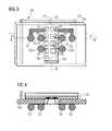
- FIG. 3shows a view of the underside of a module containing the chip according to FIG. 2 in a face-down orientation on a carrier.
- FIG. 4is a sectional view of the module according to FIG. 3 .
- FIG. 5shows a carrier for a face-up orientation of the chip.
- FIG. 6shows a first embodiment of a module with the carrier according to FIG. 5 and a chip arranged thereon in a face-up orientation.
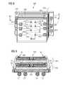
- FIG. 7illustrates in perspective representation the steps of assembling a stacked module containing two chips in a face-up arrangement on a carrier according to FIG. 5 .
- FIG. 8shows the stacked module assembled in accordance with FIG. 7 .
- FIG. 9is a sectional view of the stacked module according to FIG. 8 .
- FIG. 1shows, bordered by a dashed frame, the circuit diagram of a changeover device 21 , which is only one part of a much more extensive integrated circuit formed overall by a multilayered integration layer 20 on a semiconductor substrate 10 .
- Said circuitcan be any desired semiconductor circuit having a great multiplicity of semiconductor and metallization elements, for example a digital memory circuit.
- the circuithas a plurality of internal connection lines, which are indicated as short vertical lines in FIG. 1 , for transferring electric currents and potentials between components of the circuit and assigned contacts (not shown in FIG. 1 ) that are connected to the outside world during operation.
- connection lines L 1 : 4are provided for transferring signals.
- N4 internal connection lines L 1 : 4 are provided for transferring signals.
- N of signal connection linescan be much greater.
- Two further connection lines LDD and LSSare the “supply lines” for transferring the two potentials, VDD and VSS of the supply voltage to the components of the integrated circuit.
- a plurality of “primary” pads P 1 : 8are provided, which are formed as relatively large-area metallizations likewise on the top side of the integration layer 20 . Said pads are not shown in FIG. 1 for reasons of clarity; their spatial arrangement on the chip area is illustrated in FIG. 2 . As can be discerned in FIG. 2 , the pads P 1 : 8 form a pattern in two series which comprises two halves on both sides of a reference line Z 1 .
- the first halfcontains the odd-numbered pads P 1 , P 3 , P 5 , P 7 , and the other half contains the even-numbered pads P 2 , P 4 , P 6 , P 8 .
- the pads P 1 : 8are exposed through corresponding etched openings in an insulating cover layer 30 , which covers all the other parts of the integrated circuit of the chip.
- the supply line LSSis connected to the two pads P 5 and P 6
- the supply line LDDis connected to the two pads P 7 and P 8 .
- the changeover device 21 shown in FIG. 1forms an interface that can be changed over between the connection lines L 1 : 4 and the pads P 1 : 4 .
- the changeover device 21contains an input circuit E and a plurality of changeover switches M 1 : 4 , which are individually and fixedly-assigned to the pads P 1 : 4 . That is to say that precisely one changeover switch M is provided for each of said pads.
- the changeover switches Mare represented by the customary multiplexer symbols, with two branch connections on one side and a main connection on the other side. The two branch connections of each changeover switch M are designated by “0” and “1”.
- a further connection at each changeover switch Mis provided with an arrow in FIG. 1 and forms the control connection for applying a binary control signal.
- control signal at a changeover switch Mhas the one binary value “1”
- the changeover switchis conditioned such that its “1” branch connection is connected to its main connection. If the control signal has the other binary value, the changeover switch connects its “0” branch connection to the main connection.
- each changeover switch Mis connected to the pad P assigned thereto.
- the control connections of all the changeover switches M 1 : 4are connected to a common control line SL.
- the four internal signal connection lines L 1 : 4form two pairs, each of which is assigned to a pair of the changeover switches M 1 : 4 .
- the lines L 1 : 4are connected to the branch connections of the changeover switches M 1 : 4 in a scheme such that the changeover switches, if the control signal has the binary value “0”, connect each of the lines L 1 : 4 to the correspondingly numbered specimen of the pads P 1 : 4 .
- the changeover switches M 1 : 4then connect the odd-numbered lines L 1 , L 3 to the even-numbered pads P 2 , P 4 and the even-numbered lines L 2 , L 4 to the odd-numbered pads P 1 , P 3 . That is to say that the assignment between the half-sets of the pads P 1 : 4 , on the one hand, and two half-sets of the connection lines L 1 : 4 , on the other hand, can be reversed by means of the control signal.
- control line SLis connected to the output of the input circuit E, the input SE of which forms the control input of the entire changeover device 21 .
- Said control input SEis connected to an additional pad PM, which is formed in a similar manner to the other pads on the top side of the chip 110 , as is shown in FIG. 2 .
- the input circuit Ehas two supply potential connections, one of which is connected to the supply line LSS (or to the supply pad P 5 or P 6 ), and the other of which is connected to the supply line LDD (or to the supply pad P 7 or P 8 ).
- the input circuit Eis formed in such a way that it supplies the binary value “1” at its output precisely when the supply potential VDD (that is to say the “1” potential) is received at the control input SE. Otherwise, it supplies the binary value “0”.
- FIG. 3 and FIG. 4illustrate how the chip 110 shown in FIG. 2 can be combined in face-down orientation with a carrier 120 in order to form a module 100 , which can be placed onto a support for operation.
- FIG. 3shows the module 100 in a view from below, that is to say in a view of the underside of the carrier 120 .
- FIG. 4shows a cross section through the module 100 in accordance with the sectional plane 4 indicated in FIG. 3 , to be precise in a viewing direction indicated by arrows in FIG. 3 .
- the carrier 120composed of an insulating material, has an opening 121 , which permits access to the overlying pads P 1 : 8 of the chip 110 .
- Situated on the underside of the carrier 120are four contact pieces C 1 : 4 for signals, and two contact pieces CSS and CDD for the two supply potentials VSS and VDD.
- the contact piecesare formed as balls of soldering material. These solder balls are applied to assigned metallizations at the underside of the carrier 120 .
- the pattern of the contact pieces C 1 : 4likewise forms two half-sets on both sides of a reference line Z 2 .
- the contact pieces C 1 : 4are arranged on each side of the reference line Z 2 as pairs lying alongside one another, such that the area at the underside of the carrier 120 is utilized better in order that the contact pieces can be made significantly larger and be arranged at a larger mutual distance than the pads P 1 : 4 of the chip 110 .
- the connections between the contact pieces C 1 : 4 and the pads P 1 : 4are produced by wires that are led through the opening 121 .
- the contact piece CSSis arranged to the right of the opening 121 and connected via a wire to the nearest pad P 6 of the two pads P 6 , P 8 , which are connected to the internal connection line LSS for the supply potential VSS on the chip 110 .
- the contact piece CDDis arranged to the left of the opening 121 and connected via a wire to the nearest pad P 7 of the two pads P 5 , P 7 , which are connected to the internal connection line LDD for the supply potential VDD on the chip 110 .
- the wire connections shown in FIGS. 3 and 4are produced before the application of the solder balls, the wires being attached to the metallizations which are assigned to the contact pieces C 1 : 8 .
- the metallizations for the contact pieces C 1 , C 2 , C 5 , C 7which lie relatively far away from the opening 121 , are lengthened to close to the edge of the opening.
- each of the internal signal connection lines L 1 : 4is intended to be connected to the respectively identically numbered specimen of the contact pieces C 1 : 4 .
- the contact piece CDDis the one to which the supply potential VDD corresponding to the binary value “1” is intended to be applied during operation.
- the contact piece CSSserves for application of supply potential VSS corresponding to the binary value “0”.
- the pad P 7 and hence the internal line LDDare at VDD potential
- the pad P 6 , and hence the line LSSare at VSS potential.
- the additional pad PM connected to the control input SEhas no electrical connection to any contacts of the carrier 120 , such that the output of the control circuit E supplies the binary value “0”.
- control signal for the changeover switches M 1 : 4also goes to the binary value “0”, such that all the changeover switches connect their “0” branch connection to their main connection. Accordingly, the connection lines L 1 : 4 are connected to the contact pieces C 1 : 4 according to their numberings.
- connection lines L 1 : 4 and the contact pieces C 1 : 4are also intended to arise when the chip 110 is positioned in a face-up orientation on a carrier having, at its underside, the same pattern of contact pieces C 1 : 4 , CSS and CDD as is shown in FIG. 3 in connection with the face-down orientation.
- FIG. 5shows such a carrier 220 formed for the face-up orientation of the chip, in a view from above.
- the contact pieces C 1 : 4 , CSS and CDD situated at the underside of the carrier 220are depicted by dashed lines.
- Said contact pieceswhich are formed and arranged in exactly the same way as the contact pieces at the underside of the carrier 120 described above, are electrically connected via conductor tracks (likewise depicted by dashed lines) and metallic feedthroughs to assigned bonding pads B 1 : 4 , BSS and BDD situated as so-called “landing” pads on the top side of the carrier 220 in order to be able to attach connecting wires there.
- the total of six landing pads B 1 : 4 , BSS, BDDform two series, each having three pads on the two projecting lateral edge regions of the carrier 220 .
- One seriescomprises the odd-numbered landing pads B 1 , B 3 and the landing pad BDD.
- the other seriescomprises the even-numbered landing pads B 2 , B 4 and the landing pad BSS.
- connection pieces C 1 : 4 , CSS, CDD and the landing pads B 1 : 4 , BSS, BDDare placed such that the contact pieces of the left-hand half-set are connected to the landing pads at the left-hand edge, and that the contact pieces of the right-hand half-set are connected to the landing pads at the right-hand edge. Consequently, here as well, the connecting paths are short and do not cross one another.
- FIG. 6shows a module 200 containing the carrier 220 according to FIG. 5 and the chip 110 shown in FIG. 2 in a face-up orientation.
- the pattern of the pads P 1 : 8 of the chip 110appears mirror-inverted relative to the carrier contact pieces C 1 : 4 , CSS, CDD in comparison with a face-down orientation. That is to say that the odd-numbered pads P 1 , P 3 , P 5 , P 7 then lie on the same side of the reference line as the even-numbered contact pieces C 2 , C 4 and the contact piece CSS of the carrier and therefore also on the same side as the even-numbered landing pads B 2 , B 4 and the landing pad BSS of the carrier.
- the even-numbered pads P 2 , P 4 , P 6 , P 8lie on the same side as the odd-numbered contact pieces C 1 , C 3 and the contact piece CDD of the carrier and therefore also on the same side as the odd-numbered landing pads B 1 , B 3 and the landing pad BDD of the carrier.
- said padscan be connected to the landing pads B 1 : 4 , BSS, BDD in a crossover-free manner and in each case by a path with a very short distance, as shown by the wire connections 22 in FIG. 6 , without having to relinquish the desired assignment between the contact pieces C 1 : 4 , CSS, CDD of the carrier 220 and the internal connections L 1 : 4 , LSS, LDD of the integrated circuit of the chip 110 .
- connection lines L 1 : 4are connected to the contact pieces C 1 : 4 according to their numberings and that the connection line LSS is connected to the contact piece CSS, and that the connection line LDD is connected to the contact piece CDD.
- the desired assignmentis produced by connecting the pad P 5 to the landing pad BSS.
- the desired assignmentis produced by connecting the pad P 8 to the landing pad BDD.
- the desired assignment between L 1 : 4 and C 1 : 4can be achieved by ensuring that, during operation, the control signal on the control line SL for the changeover switches M 1 : 4 of the interface circuit 21 has the binary value “1”. For this purpose it suffices to connect the additional pad PM to the landing pad BDD, as is shown by the wire 23 in FIG. 6 . Consequently, the control input SE of the changeover device 21 receives the VDD potential, such that the output of the input circuit E and hence the control line SL go to “1”.
- the primary pads P 1 : 4 , P 5 , P 8 and the additional pad PMare likewise used as bonding pads in order to directly attach the bonding wires 22 , 23 there.
- a type of connectioncan pose certain problems if the primary pads and the additional pad are arranged in the central region of the chip area, as shown.
- a first problemis that the bonding wires in the case of such an arrangement are relatively long, and hence sensitive to mechanical effects that may occur during the bonding process by means of the bonding machine and during the encapsulation of the module.
- a second problemarises if a plurality of chips in a face-up orientation is intended to be stacked one above another in a module. This is because in the case of the wire routing shown in FIG. 6 , it is difficult to arrange the required spacer between the stacked chips without mechanically stressing the wires.
- the integration processis ended after the formation of the first metallization layer. If the front side of the finished chip is intended to exhibit the second pad position, the integration process is continued and ended only after the formation of the additional metallization layer. That positioning for which the demand is greater is advantageously chosen for the primary pads. This is economic because the average outlay for chip-making is then the least.
- FIG. 7One example of the formation of a circuit module containing chips having the additional metallization layer mentioned above is shown in FIG. 7 .
- the production of this moduleis begun with a construction that is like the face-down module 200 according to FIG. 6 , but with the difference that the chip 210 situated on the carrier 220 has an additional metallization layer 40 at the very top. Otherwise, the chip 210 is like the chip 110 shown in FIG. 2 , including the changeover device 21 shown in FIG. 1 .
- the additional metallization layer 40is situated above the cover layer 30 , in which the centrally positioned primary pads P 1 : 8 and the additional pad PM are exposed.
- the primary pads P 1 : 4are connected via feedthroughs and conductor tracks of the layer 40 to secondary pads A 1 : 4 , ASS, ADD which are positioned on the top side of the layer 40 near those two edges which are adjacent to the landing pads of the carrier 220 .
- the secondary pads A 1 : 4 , ASS, ADDare connected to the respectively adjacent landing pads B 1 : 4 , BSS, BDD of the carrier by means of wires, as shown in FIG. 7 .
- the arrangementis such that, by means of these short wires, the secondary pads and the conductor tracks of the layer 40 , the same connections between the landing pads B 1 : 4 , BSS, BDD of the carrier 220 and the primary pads P 1 : 4 , P 5 , P 8 of the chip 210 are produced as are created by the long bonding wires 22 in the module 200 according to FIG. 6 .
- the construction of the chip 210 with the carrier 220 as shown in FIG. 7functions in exactly the same way as has been described above for the module 200 according to FIG. 6 .
- This constructionhas the advantage of short wire connections by virtue of the position of the secondary pads A 1 : 4 , ASS, ADD near the edges.
- a further advantage of this pad positionis the stackability of a plurality of chips one above another.
- a relatively large-area spacer 230can be adhesively bonded onto the front side of the chip 210 wired with the carrier 220 , without disturbing the wire connections.
- a second chip 310 in face-up orientationcan then be adhesively bonded onto said spacer 230 , said second chip likewise having bonding pads at its front side, which are then connected via further bonding wires to landing pads at the carrier.
- said second chip 310is formed in exactly the same way as the chip 210 , and its secondary pads A 1 : 4 , ASS, ADD are connected to the landing pads B 1 : 4 , BSS, BDD of the carrier 220 according to the same scheme as in the case of the chip 210 .
- the two chips 210 and 310are thereby connected in parallel, in which case individual addressing can be effected by means of code words.
- Such an arrangementmay be expedient e.g. when memory chips are involved, which are often operated in parallel connection.
- the chips on the carriercan contain the same integrated circuit in each case or even to be connected in parallel. If other or additional electrical connections to the outside world are required for the second chip, the carrier can be provided with corresponding additional contact pieces and assigned landing pads. Furthermore, it should be mentioned that with the technique illustrated in FIG. 7 , it is also possible, of course, to stack more than two chips in face-up orientation one above another, in each case with interposition of a spacer. Moreover, in an embodiment where multiple chips are stacked in a face-up orientation, it is not necessary for the top-most chip to have the bonding positioned near the edges of the chip.
- FIG. 8shows in a perspective view, for the sake of clarity, the module 300 composed of the carrier 220 , the two chips 210 , 220 and the spacer 230 after completion of the wiring.
- FIG. 9is a sectional view of this module according to the sectional profile 9 depicted by dashed lines in FIG. 8 , and in a viewing direction indicated by the arrows. The position (which cannot be illustrated in FIG. 5 ) of the feedthroughs at the carrier 220 and also the ball-like shape of the contact pieces at the underside of the carrier 220 can be discerned in FIG. 9 .
- the moduleis encapsulated all around (with the exception of the underside) in the customary manner in order to form a robust housing.
- the embodiments described above with reference to the figuresare only examples, and the highly simplified representations in the drawings are merely intended to illustrate the principle of the invention.
- the various partsare not depicted to scale, particularly as far as the thickness of the various layers is concerned.
- the primary pads, the contact pieces at the carrier and also the bonding pads and the landing padsin each case form a pattern which is precisely mirror-symmetrical with respect to the relevant reference line Z 1 or Z 2 .
- Such a symmetryis advantageous, but not a necessary prerequisite.
- the reference lines Z 1 , Z 2need not be congruent with one another; they can also lie laterally offset with respect to one another or be angularly offset with respect to one another to a certain extent.
- the principle of the inventioncan also be applied in conjunction with chips in which primary pads are integrated at the edge regions on the chips.
- the primary pads in the face-up orientation of the moduleas bonding pads, such that no further metallization layer is required for forming secondary pads.
- the additional padshould also lie near the edge in order to be able to produce its electrical connection to the carrier via a short wire connection that keeps the central region of the chip area free. If the intention is to arrange a chip with primary pads near the edges in face-down orientation on a carrier having the structure of the carrier 120 according to FIGS. 3 and 4 , then the connection of the primary pads P 1 : 8 to the central feedthroughs situated in the carrier 120 can be effected by means of an additional metallization layer integrated on the chip.
- connection between the control line SL and that contact piece CDD of the carrier which is selected for the supply potential VDDis produced if the chips are arranged in face-up orientation.
- the control line SLremains without connection to CDD.
- a corresponding variant of the changeover deviceneed differ from the changeover device 21 according to FIG. 1 only in that the 0 connections and the 1 connections of the changeover switches M 1 : 4 are interchanged.
- the input circuit E of the changeover device 21can be any suitable circuit which supplies the binary value “1” if the control input SE receives the “1” potential VDD, and supplies the binary value “0” if the control input SE is potential-free.
- a very simple embodimentconsists in connecting the control input SE (or the additional pad PM) directly to the control line SL and connecting it to the supply line LSS in high-resistance fashion.
- the input circuit Ecan also be formed in such a way that it supplies the binary value “1” precisely when the control input SE receives the “1” potential VDD, and supplies the binary value “0” precisely when the control input SE receives the “0” potential VSS.
- the additional pad PMmust always be connected to a supply contact piece of the carrier, either to a VDD contact piece or to a VSS contact piece, depending on the desired switching state of the changeover device 21 .
- FIG. 3illustrates such a connection between PM and CSS by means of the wire connection depicted in a dashed manner.
- the carriers 120 , 220contain, for each of the two supply potentials VSS and VDD, in each case only one contact piece BSS and BDD, respectively. If desired, it is possible to provide for each of the supply potentials in each case two contact pieces which form a similar arrangement to the signal contact pieces C 1 : 4 , a VSS contact piece and a VDD contact piece in each case lying on each side of the reference line Z 2 .
- each of the two VSS contact piecesis connected to the respectively nearest pad of the pad pair P 5 , P 6
- each of the VDD contact piecesis connected to the respectively nearest pad of the pad pair P 7 , P 8 .
- corresponding additional supply landing padsare to be provided in order to be able to produce all of these connections.
- the support of the carrierwhich has the mating contacts with respect to the contact pieces of the carrier, can be directly a circuit board, which can also carry other modules as well.
- the supportcan also be a base which is itself part of the module and, for its part, is provided with external contacts for electrically connecting the module to a circuit board.
Landscapes
- Engineering & Computer Science (AREA)
- Power Engineering (AREA)
- Microelectronics & Electronic Packaging (AREA)
- Physics & Mathematics (AREA)
- Condensed Matter Physics & Semiconductors (AREA)
- General Physics & Mathematics (AREA)
- Computer Hardware Design (AREA)
- Semiconductor Integrated Circuits (AREA)
Abstract
Description
- This application claims foreign priority benefits under 35 U.S.C. §119 to co-pending German patent
application number DE 10 2006 042 775.0-33, filed 12 Sep. 2006. This related patent application is herein incorporated by reference in its entirety. - 1. Field of the Invention
- The invention relates to a method of producing a circuit module containing at least one chip containing an integrated circuit on a carrier. The invention furthermore relates to an integrated circuit module.
- 2. Description of the Related Art
- Integrated circuits are usually produced by means of a multiplicity of photolithographic steps on a semiconductor substrate, normally a large number of such circuits being formed simultaneously on a relatively large-area semiconductor slice, a so-called “wafer”. After completion of the integration, the wafer is diced in order to obtain the individual circuits in the form of small “chips”. Each integrated circuit contains a plurality of contact areas, referred to hereinafter as “primary pads”, which are connected via individually assigned internal connection lines to other internal components of the circuit in order to transfer the electric currents and potentials required for operation.
- Said pads form the connection points for the external connections of the integrated circuit to the outside world. Since the external connections cannot be miniaturized to the same extent as the integrated internal components, the pads must be relatively large in order to offer enough engagement area for the attachment of wires or for soldering connections.
- A chip configured in the manner described above is positioned on the top side of a carrier, at which contact areas are situated, which are then electrically connected to the pads of the chip. For their part, said contact areas are connected to assigned contact pieces at the carrier, which contact pieces project at the underside of the carrier and can be formed as plug pins or as solder balls in order to fit or solder them together with corresponding mating contacts on a support.
- There are two options for the relative orientation between chip and carrier when assembling these two parts. In order to describe the respective orientation, the side of the chip which is remote from the substrate and on which the primary pads are situated is referred to hereinafter as “front side”, while the opposite side, where the substrate is situated, is referred to as “rear side”.
- The first option is a so-called “face-up” orientation. In this case, the chip is placed with its rear side downward onto the top side of the carrier, such that the primary pads are accessible for attaching connecting wires, the other ends of which are attached to the assigned contact areas of the carrier. In order to enable this “bonding”, the carrier contact areas are arranged on edge regions of the carrier which project laterally beyond the chip.
- The second option is a so-called “face-down” orientation. In this case, the chip is placed with its front side downward onto the top side of the carrier, the contact areas being arranged on the underside of the carrier in such a way that they can be connected to the pads of the chip via wires through an opening in the carrier.
- The decision as to which of the two possible orientations of a chip relative to the carrier in a circuit module to be chosen depends on various circumstances. Depending on the stipulations for the carrier, one orientation of the chip may be more favorable than the other in order to produce the conductive connections between the primary pads of the chip and the carrier. Another standpoint is whether the module contains only a single chip or a plurality of chips stacked one above another on the carrier. In the case of a single-chip module, face-down orientation may be preferable because conducting line paths that are as short as possible then result. In the case of a stacked module, however, face-up orientation may be more advantageous because it is simpler to wire the pads of all the chips with the carrier.
- A manufacturer of circuit modules should therefore be flexible in the choice of chip orientation with regard to the carrier.
- One embodiment provides an integrated circuit module comprising a chip, the chip comprising a substrate with a first main area and a second main area, the first main area comprising two half-sets of pads, the chip further comprising an integrated circuit with components and two half-sets of connection lines, the connection lines connecting the components of the integrated circuit to the pads, the integrated circuit further comprising a changeover device, the changeover device having two switching states in order to interchange the electrical assignment between the half-sets of the connection lines and the half-sets of the pads. The integrated circuit further comprises a carrier, the carrier comprising contact pieces. The chip is arranged on the carrier with one of the two main areas of the chip facing the carrier and the contact pieces of the carrier are connected to the pads of the chip. One of the two switching states of the changeover device is selected, depending on which of the two main areas of the chip is the area facing the carrier.
- The features of embodiments will become clear from the following description, taking in conjunction with the accompanying drawings. It is to be noted, however, that the accompanying drawings illustrate only typical embodiments and are, therefore, not to be considered limiting of the scope of the invention. It may admit other equally effective embodiments.
FIG. 1 shows the schematic circuit diagram of a changeover device that is contained in the integrated circuit of a chip and serves for interchanging the assignment between internal connection lines and pads of the chip.FIG. 2 shows the arrangement of the pads on the front side of a chip containing the changeover device according toFIG. 1 .FIG. 3 shows a view of the underside of a module containing the chip according toFIG. 2 in a face-down orientation on a carrier.FIG. 4 is a sectional view of the module according toFIG. 3 .FIG. 5 shows a carrier for a face-up orientation of the chip.FIG. 6 shows a first embodiment of a module with the carrier according toFIG. 5 and a chip arranged thereon in a face-up orientation.FIG. 7 illustrates in perspective representation the steps of assembling a stacked module containing two chips in a face-up arrangement on a carrier according toFIG. 5 .FIG. 8 shows the stacked module assembled in accordance withFIG. 7 .FIG. 9 is a sectional view of the stacked module according toFIG. 8 .- In the figures, elements of identical type are designated by the same upper-case letters in each case, succeeded by a respective number for the purpose of closer identification. In the description below, a colon between two such numbers should be read as the word “to”. Thus, by way of example, “pads P1:8” should be read as “pads P1 to P8”.
FIG. 1 shows, bordered by a dashed frame, the circuit diagram of achangeover device 21, which is only one part of a much more extensive integrated circuit formed overall by amultilayered integration layer 20 on asemiconductor substrate 10. Said circuit can be any desired semiconductor circuit having a great multiplicity of semiconductor and metallization elements, for example a digital memory circuit. The circuit has a plurality of internal connection lines, which are indicated as short vertical lines inFIG. 1 , for transferring electric currents and potentials between components of the circuit and assigned contacts (not shown inFIG. 1 ) that are connected to the outside world during operation.- In order to retain clarity in the representation of the drawing, it is assumed below as an example that N=4 internal connection lines L1:4 are provided for transferring signals. In reality, the number N of signal connection lines can be much greater. Two further connection lines LDD and LSS are the “supply lines” for transferring the two potentials, VDD and VSS of the supply voltage to the components of the integrated circuit.
- In order to be able to connect the N=4 signal connection lines L1:4 and the supply connection lines LSS and LDD to the outside world, a plurality of “primary” pads P1:8 are provided, which are formed as relatively large-area metallizations likewise on the top side of the
integration layer 20. Said pads are not shown inFIG. 1 for reasons of clarity; their spatial arrangement on the chip area is illustrated inFIG. 2 . As can be discerned inFIG. 2 , the pads P1:8 form a pattern in two series which comprises two halves on both sides of a reference line Z1. The first half contains the odd-numbered pads P1, P3, P5, P7, and the other half contains the even-numbered pads P2, P4, P6, P8. The pads P1:8 are exposed through corresponding etched openings in an insulatingcover layer 30, which covers all the other parts of the integrated circuit of the chip. - In
FIG. 1 , the connections from thechangeover device 21 to the primary pads P1:8 are indicated by correspondingly designated arrows. Accordingly, the N=4 primary pads P1:4 are assigned to the N=4 signal connection lines L1:4. The supply line LSS is connected to the two pads P5 and P6, and the supply line LDD is connected to the two pads P7 and P8. - The
changeover device 21 shown inFIG. 1 forms an interface that can be changed over between the connection lines L1:4 and the pads P1:4. Thechangeover device 21 contains an input circuit E and a plurality of changeover switches M1:4, which are individually and fixedly-assigned to the pads P1:4. That is to say that precisely one changeover switch M is provided for each of said pads. InFIG. 1 the changeover switches M are represented by the customary multiplexer symbols, with two branch connections on one side and a main connection on the other side. The two branch connections of each changeover switch M are designated by “0” and “1”. A further connection at each changeover switch M is provided with an arrow inFIG. 1 and forms the control connection for applying a binary control signal. If the control signal at a changeover switch M has the one binary value “1”, then the changeover switch is conditioned such that its “1” branch connection is connected to its main connection. If the control signal has the other binary value, the changeover switch connects its “0” branch connection to the main connection. - As indicated by arrows in
FIG. 1 , the main connection of each changeover switch M is connected to the pad P assigned thereto. Within thechangeover device circuit 21, according toFIG. 1 , the control connections of all the changeover switches M1:4 are connected to a common control line SL. The four internal signal connection lines L1:4 form two pairs, each of which is assigned to a pair of the changeover switches M1:4. The lines L1:4 are connected to the branch connections of the changeover switches M1:4 in a scheme such that the changeover switches, if the control signal has the binary value “0”, connect each of the lines L1:4 to the correspondingly numbered specimen of the pads P1:4. If the control signal has the binary value “1”, then a mirror-inverted connecting pattern results: the changeover switches M1:4 then connect the odd-numbered lines L1, L3 to the even-numbered pads P2, P4 and the even-numbered lines L2, L4 to the odd-numbered pads P1, P3. That is to say that the assignment between the half-sets of the pads P1:4, on the one hand, and two half-sets of the connection lines L1:4, on the other hand, can be reversed by means of the control signal. - It should be assumed for the exemplary embodiments described here that the binary value “1” of the control signal corresponds to the supply potential VDD, and that the binary value “0” of the control signal corresponds to the supply potential VSS. In accordance with
FIG. 1 , the control line SL is connected to the output of the input circuit E, the input SE of which forms the control input of theentire changeover device 21. Said control input SE is connected to an additional pad PM, which is formed in a similar manner to the other pads on the top side of thechip 110, as is shown inFIG. 2 . The input circuit E has two supply potential connections, one of which is connected to the supply line LSS (or to the supply pad P5 or P6), and the other of which is connected to the supply line LDD (or to the supply pad P7 or P8). The input circuit E is formed in such a way that it supplies the binary value “1” at its output precisely when the supply potential VDD (that is to say the “1” potential) is received at the control input SE. Otherwise, it supplies the binary value “0”. FIG. 3 andFIG. 4 illustrate how thechip 110 shown inFIG. 2 can be combined in face-down orientation with acarrier 120 in order to form amodule 100, which can be placed onto a support for operation.FIG. 3 shows themodule 100 in a view from below, that is to say in a view of the underside of thecarrier 120.FIG. 4 shows a cross section through themodule 100 in accordance with thesectional plane 4 indicated inFIG. 3 , to be precise in a viewing direction indicated by arrows inFIG. 3 .- The
carrier 120, composed of an insulating material, has anopening 121, which permits access to the overlying pads P1:8 of thechip 110. Situated on the underside of thecarrier 120 are four contact pieces C1:4 for signals, and two contact pieces CSS and CDD for the two supply potentials VSS and VDD. In the case shown, the contact pieces are formed as balls of soldering material. These solder balls are applied to assigned metallizations at the underside of thecarrier 120. - The pattern of the contact pieces C1:4 likewise forms two half-sets on both sides of a reference line Z2. In the case shown, the contact pieces C1:4 are arranged on each side of the reference line Z2 as pairs lying alongside one another, such that the area at the underside of the
carrier 120 is utilized better in order that the contact pieces can be made significantly larger and be arranged at a larger mutual distance than the pads P1:4 of thechip 110. The connections between the contact pieces C1:4 and the pads P1:4 are produced by wires that are led through theopening 121. Said connections are placed such that the contact pieces C1, C3 of the left-hand half-set are connected to the pads P1, P3 of the left-hand half-set, and that the contact pieces C2, C4 of the right-hand half-set are connected to the pads P2, P4 of the right-hand half-set. This has the advantage that the connecting paths are as short as possible and do not cross one another. - The contact piece CSS is arranged to the right of the
opening 121 and connected via a wire to the nearest pad P6 of the two pads P6, P8, which are connected to the internal connection line LSS for the supply potential VSS on thechip 110. The contact piece CDD is arranged to the left of theopening 121 and connected via a wire to the nearest pad P7 of the two pads P5, P7, which are connected to the internal connection line LDD for the supply potential VDD on thechip 110. - The wire connections shown in
FIGS. 3 and 4 are produced before the application of the solder balls, the wires being attached to the metallizations which are assigned to the contact pieces C1:8. In order to keep all the wires as short as possible, the metallizations for the contact pieces C1, C2, C5, C7, which lie relatively far away from theopening 121, are lengthened to close to the edge of the opening. - During the operation of the module, each of the internal signal connection lines L1:4 is intended to be connected to the respectively identically numbered specimen of the contact pieces C1:4. The contact piece CDD is the one to which the supply potential VDD corresponding to the binary value “1” is intended to be applied during operation. The contact piece CSS serves for application of supply potential VSS corresponding to the binary value “0”. During operation, therefore, the pad P7 and hence the internal line LDD are at VDD potential, and the pad P6, and hence the line LSS, are at VSS potential. The additional pad PM connected to the control input SE has no electrical connection to any contacts of the
carrier 120, such that the output of the control circuit E supplies the binary value “0”. Consequently, the control signal for the changeover switches M1:4 also goes to the binary value “0”, such that all the changeover switches connect their “0” branch connection to their main connection. Accordingly, the connection lines L1:4 are connected to the contact pieces C1:4 according to their numberings. - The same assignment between the connection lines L1:4 and the contact pieces C1:4 is also intended to arise when the
chip 110 is positioned in a face-up orientation on a carrier having, at its underside, the same pattern of contact pieces C1:4, CSS and CDD as is shown inFIG. 3 in connection with the face-down orientation.FIG. 5 shows such acarrier 220 formed for the face-up orientation of the chip, in a view from above. The contact pieces C1:4, CSS and CDD situated at the underside of thecarrier 220 are depicted by dashed lines. Said contact pieces, which are formed and arranged in exactly the same way as the contact pieces at the underside of thecarrier 120 described above, are electrically connected via conductor tracks (likewise depicted by dashed lines) and metallic feedthroughs to assigned bonding pads B1:4, BSS and BDD situated as so-called “landing” pads on the top side of thecarrier 220 in order to be able to attach connecting wires there. - The total of six landing pads B1:4, BSS, BDD form two series, each having three pads on the two projecting lateral edge regions of the
carrier 220. One series comprises the odd-numbered landing pads B1, B3 and the landing pad BDD. The other series comprises the even-numbered landing pads B2, B4 and the landing pad BSS. - The connections between the contact pieces C1:4, CSS, CDD and the landing pads B1:4, BSS, BDD are placed such that the contact pieces of the left-hand half-set are connected to the landing pads at the left-hand edge, and that the contact pieces of the right-hand half-set are connected to the landing pads at the right-hand edge. Consequently, here as well, the connecting paths are short and do not cross one another.
FIG. 6 shows amodule 200 containing thecarrier 220 according toFIG. 5 and thechip 110 shown inFIG. 2 in a face-up orientation. In the case of a face-up orientation, the pattern of the pads P1:8 of thechip 110 appears mirror-inverted relative to the carrier contact pieces C1:4, CSS, CDD in comparison with a face-down orientation. That is to say that the odd-numbered pads P1, P3, P5, P7 then lie on the same side of the reference line as the even-numbered contact pieces C2, C4 and the contact piece CSS of the carrier and therefore also on the same side as the even-numbered landing pads B2, B4 and the landing pad BSS of the carrier. The even-numbered pads P2, P4, P6, P8 lie on the same side as the odd-numbered contact pieces C1, C3 and the contact piece CDD of the carrier and therefore also on the same side as the odd-numbered landing pads B1, B3 and the landing pad BDD of the carrier.- Despite the mirror-inverted alignment of the pads P1:8, said pads can be connected to the landing pads B1:4, BSS, BDD in a crossover-free manner and in each case by a path with a very short distance, as shown by the
wire connections 22 inFIG. 6 , without having to relinquish the desired assignment between the contact pieces C1:4, CSS, CDD of thecarrier 220 and the internal connections L1:4, LSS, LDD of the integrated circuit of thechip 110. As stated, the desired assignment consists in the fact that, during operation, the connection lines L1:4 are connected to the contact pieces C1:4 according to their numberings and that the connection line LSS is connected to the contact piece CSS, and that the connection line LDD is connected to the contact piece CDD. - For the line LSS, the desired assignment is produced by connecting the pad P5 to the landing pad BSS. For the line LDD, the desired assignment is produced by connecting the pad P8 to the landing pad BDD.
- The desired assignment between L1:4 and C1:4 can be achieved by ensuring that, during operation, the control signal on the control line SL for the changeover switches M1:4 of the
interface circuit 21 has the binary value “1”. For this purpose it suffices to connect the additional pad PM to the landing pad BDD, as is shown by thewire 23 inFIG. 6 . Consequently, the control input SE of thechangeover device 21 receives the VDD potential, such that the output of the input circuit E and hence the control line SL go to “1”. - During the production of the wire connections shown in
FIG. 6 , the primary pads P1:4, P5, P8 and the additional pad PM are likewise used as bonding pads in order to directly attach thebonding wires FIG. 6 , it is difficult to arrange the required spacer between the stacked chips without mechanically stressing the wires. - These problems can be eliminated by ensuring that the bonding pads of the chip are positioned near the edges of the chip. For a face-down arrangement, by contrast, a central position of pads is more advantageous. In order to be able to realize the one or the other of the two pad positions as required, it is advantageous to configure the integration process for the pads in such a way that, firstly, a metallization layer with primary pads in a first positioning is formed and, as required, there is integrated above said layer an additional metallization layer, on which are situated secondary pads as bonding pads in the second positioning and at which suitable feedthroughs and conductor tracks are provided in order to connect said secondary pads to the primary pads of the underlying first metallization layer.
- If the finished chip is intended to exhibit the first pad position on its front side, the integration process is ended after the formation of the first metallization layer. If the front side of the finished chip is intended to exhibit the second pad position, the integration process is continued and ended only after the formation of the additional metallization layer. That positioning for which the demand is greater is advantageously chosen for the primary pads. This is economic because the average outlay for chip-making is then the least.
- One example of the formation of a circuit module containing chips having the additional metallization layer mentioned above is shown in
FIG. 7 . The production of this module is begun with a construction that is like the face-down module 200 according toFIG. 6 , but with the difference that thechip 210 situated on thecarrier 220 has anadditional metallization layer 40 at the very top. Otherwise, thechip 210 is like thechip 110 shown inFIG. 2 , including thechangeover device 21 shown inFIG. 1 . Theadditional metallization layer 40 is situated above thecover layer 30, in which the centrally positioned primary pads P1:8 and the additional pad PM are exposed. The primary pads P1:4 are connected via feedthroughs and conductor tracks of thelayer 40 to secondary pads A1:4, ASS, ADD which are positioned on the top side of thelayer 40 near those two edges which are adjacent to the landing pads of thecarrier 220. - After the joining together of the
chip 210 with thecarrier 220, the secondary pads A1:4, ASS, ADD are connected to the respectively adjacent landing pads B1:4, BSS, BDD of the carrier by means of wires, as shown inFIG. 7 . The arrangement is such that, by means of these short wires, the secondary pads and the conductor tracks of thelayer 40, the same connections between the landing pads B1:4, BSS, BDD of thecarrier 220 and the primary pads P1:4, P5, P8 of thechip 210 are produced as are created by thelong bonding wires 22 in themodule 200 according toFIG. 6 . In the embodiment according toFIG. 7 , thewiring 23 shown inFIG. 6 between the additional pad PM and the landing pad BDD is replaced by an additional conductor track at themetallization layer 40, which connects the additional pad PM to the secondary pad ADD, which is wired with the landing pad BDD of thecarrier 220, which pad is at the supply potential VDD during operation. - Consequently, the construction of the
chip 210 with thecarrier 220 as shown inFIG. 7 functions in exactly the same way as has been described above for themodule 200 according toFIG. 6 . This construction has the advantage of short wire connections by virtue of the position of the secondary pads A1:4, ASS, ADD near the edges. A further advantage of this pad position is the stackability of a plurality of chips one above another. As likewise shown inFIG. 7 , a relatively large-area spacer 230 can be adhesively bonded onto the front side of thechip 210 wired with thecarrier 220, without disturbing the wire connections. Asecond chip 310 in face-up orientation can then be adhesively bonded onto saidspacer 230, said second chip likewise having bonding pads at its front side, which are then connected via further bonding wires to landing pads at the carrier. In the example shown, saidsecond chip 310 is formed in exactly the same way as thechip 210, and its secondary pads A1:4, ASS, ADD are connected to the landing pads B1:4, BSS, BDD of thecarrier 220 according to the same scheme as in the case of thechip 210. The twochips - It is not mandatory, however, for the chips on the carrier to contain the same integrated circuit in each case or even to be connected in parallel. If other or additional electrical connections to the outside world are required for the second chip, the carrier can be provided with corresponding additional contact pieces and assigned landing pads. Furthermore, it should be mentioned that with the technique illustrated in
FIG. 7 , it is also possible, of course, to stack more than two chips in face-up orientation one above another, in each case with interposition of a spacer. Moreover, in an embodiment where multiple chips are stacked in a face-up orientation, it is not necessary for the top-most chip to have the bonding positioned near the edges of the chip. FIG. 8 shows in a perspective view, for the sake of clarity, themodule 300 composed of thecarrier 220, the twochips spacer 230 after completion of the wiring.FIG. 9 is a sectional view of this module according to the sectional profile9 depicted by dashed lines inFIG. 8 , and in a viewing direction indicated by the arrows. The position (which cannot be illustrated inFIG. 5 ) of the feedthroughs at thecarrier 220 and also the ball-like shape of the contact pieces at the underside of thecarrier 220 can be discerned inFIG. 9 . After the assembly of the construction shown inFIGS. 8 and 9 , the module is encapsulated all around (with the exception of the underside) in the customary manner in order to form a robust housing.- The embodiments described above with reference to the figures are only examples, and the highly simplified representations in the drawings are merely intended to illustrate the principle of the invention. The various parts are not depicted to scale, particularly as far as the thickness of the various layers is concerned. In the examples shown, the primary pads, the contact pieces at the carrier and also the bonding pads and the landing pads in each case form a pattern which is precisely mirror-symmetrical with respect to the relevant reference line Z1 or Z2. Such a symmetry is advantageous, but not a necessary prerequisite. Moreover, it is not mandatory for the reference lines Z1 and Z2 to coincide precisely with the center line of the module, as is shown in the figures. Moreover, the reference lines Z1, Z2 need not be congruent with one another; they can also lie laterally offset with respect to one another or be angularly offset with respect to one another to a certain extent.
- The invention is not restricted to the embodiments described. For the realization of the invention, various other variants and also further configurations are possible, some of which are indicated below.
- The principle of the invention can also be applied in conjunction with chips in which primary pads are integrated at the edge regions on the chips. In this case, it is possible to use the primary pads in the face-up orientation of the module as bonding pads, such that no further metallization layer is required for forming secondary pads. In this case, the additional pad should also lie near the edge in order to be able to produce its electrical connection to the carrier via a short wire connection that keeps the central region of the chip area free. If the intention is to arrange a chip with primary pads near the edges in face-down orientation on a carrier having the structure of the
carrier 120 according toFIGS. 3 and 4 , then the connection of the primary pads P1:8 to the central feedthroughs situated in thecarrier 120 can be effected by means of an additional metallization layer integrated on the chip. - In the case of the embodiment described in FIGS.7 to9, the connection between the control line SL and that contact piece CDD of the carrier which is selected for the supply potential VDD is produced if the chips are arranged in face-up orientation. In the case of face-down orientation according to
FIGS. 3 and 4 , the control line SL remains without connection to CDD. As an alternative, it is also possible to form the changeover device between the primary signal pads P1:4 and the connection lines L1:4 in such a way as to result in the desired assignment between said lines and the contact pieces of the carrier if the connection between SL and CDD is produced in the case of face-down orientation and is lacking in the case of face-up orientation. A corresponding variant of the changeover device need differ from thechangeover device 21 according toFIG. 1 only in that the 0 connections and the 1 connections of the changeover switches M1:4 are interchanged. - The input circuit E of the
changeover device 21 can be any suitable circuit which supplies the binary value “1” if the control input SE receives the “1” potential VDD, and supplies the binary value “0” if the control input SE is potential-free. A very simple embodiment consists in connecting the control input SE (or the additional pad PM) directly to the control line SL and connecting it to the supply line LSS in high-resistance fashion. - However, the input circuit E can also be formed in such a way that it supplies the binary value “1” precisely when the control input SE receives the “1” potential VDD, and supplies the binary value “0” precisely when the control input SE receives the “0” potential VSS. In the case of such an embodiment (which can be realized in the simplest case by direct connection between SE and the control line SL), the additional pad PM must always be connected to a supply contact piece of the carrier, either to a VDD contact piece or to a VSS contact piece, depending on the desired switching state of the
changeover device 21.FIG. 3 illustrates such a connection between PM and CSS by means of the wire connection depicted in a dashed manner. - In the embodiments illustrated in the drawings, the
carriers - Finally, it should also be mentioned that the support of the carrier, which has the mating contacts with respect to the contact pieces of the carrier, can be directly a circuit board, which can also carry other modules as well. However, the support can also be a base which is itself part of the module and, for its part, is provided with external contacts for electrically connecting the module to a circuit board.
- While the foregoing is directed to embodiments of the present invention, other and further embodiments of the invention may be devised without departing from the basic scope thereof, and the scope thereof is determined by the claims that follow.
Claims (26)
Applications Claiming Priority (2)
| Application Number | Priority Date | Filing Date | Title |
|---|---|---|---|
| DE102006042775ADE102006042775B3 (en) | 2006-09-12 | 2006-09-12 | Circuit module and method for manufacturing a circuit module |
| DE102006042775.0-33 | 2006-09-12 |
Publications (2)
| Publication Number | Publication Date |
|---|---|
| US20080061423A1true US20080061423A1 (en) | 2008-03-13 |
| US7855463B2 US7855463B2 (en) | 2010-12-21 |
Family
ID=39105442
Family Applications (1)
| Application Number | Title | Priority Date | Filing Date |
|---|---|---|---|
| US11/853,995Expired - Fee RelatedUS7855463B2 (en) | 2006-09-12 | 2007-09-12 | Method for producing a circuit module comprising at least one integrated circuit |
Country Status (2)
| Country | Link |
|---|---|
| US (1) | US7855463B2 (en) |
| DE (1) | DE102006042775B3 (en) |
Cited By (23)
| Publication number | Priority date | Publication date | Assignee | Title |
|---|---|---|---|---|
| US8405207B1 (en)* | 2011-10-03 | 2013-03-26 | Invensas Corporation | Stub minimization for wirebond assemblies without windows |
| US8436457B2 (en) | 2011-10-03 | 2013-05-07 | Invensas Corporation | Stub minimization for multi-die wirebond assemblies with parallel windows |
| US8436477B2 (en) | 2011-10-03 | 2013-05-07 | Invensas Corporation | Stub minimization using duplicate sets of signal terminals in assemblies without wirebonds to package substrate |
| US8441111B2 (en) | 2011-10-03 | 2013-05-14 | Invensas Corporation | Stub minimization for multi-die wirebond assemblies with parallel windows |
| US8502390B2 (en) | 2011-07-12 | 2013-08-06 | Tessera, Inc. | De-skewed multi-die packages |
| US8513817B2 (en) | 2011-07-12 | 2013-08-20 | Invensas Corporation | Memory module in a package |
| US8513813B2 (en) | 2011-10-03 | 2013-08-20 | Invensas Corporation | Stub minimization using duplicate sets of terminals for wirebond assemblies without windows |
| US8525327B2 (en) | 2011-10-03 | 2013-09-03 | Invensas Corporation | Stub minimization for assemblies without wirebonds to package substrate |
| US8670261B2 (en) | 2011-10-03 | 2014-03-11 | Invensas Corporation | Stub minimization using duplicate sets of signal terminals |
| US8787034B2 (en) | 2012-08-27 | 2014-07-22 | Invensas Corporation | Co-support system and microelectronic assembly |
| US8823165B2 (en) | 2011-07-12 | 2014-09-02 | Invensas Corporation | Memory module in a package |
| US8848392B2 (en) | 2012-08-27 | 2014-09-30 | Invensas Corporation | Co-support module and microelectronic assembly |
| US8848391B2 (en) | 2012-08-27 | 2014-09-30 | Invensas Corporation | Co-support component and microelectronic assembly |
| US8917532B2 (en) | 2011-10-03 | 2014-12-23 | Invensas Corporation | Stub minimization with terminal grids offset from center of package |
| US8981547B2 (en) | 2011-10-03 | 2015-03-17 | Invensas Corporation | Stub minimization for multi-die wirebond assemblies with parallel windows |
| US9070423B2 (en) | 2013-06-11 | 2015-06-30 | Invensas Corporation | Single package dual channel memory with co-support |
| US9123555B2 (en) | 2013-10-25 | 2015-09-01 | Invensas Corporation | Co-support for XFD packaging |
| US9281296B2 (en) | 2014-07-31 | 2016-03-08 | Invensas Corporation | Die stacking techniques in BGA memory package for small footprint CPU and memory motherboard design |
| US9368477B2 (en) | 2012-08-27 | 2016-06-14 | Invensas Corporation | Co-support circuit panel and microelectronic packages |
| US9484080B1 (en) | 2015-11-09 | 2016-11-01 | Invensas Corporation | High-bandwidth memory application with controlled impedance loading |
| US9679613B1 (en) | 2016-05-06 | 2017-06-13 | Invensas Corporation | TFD I/O partition for high-speed, high-density applications |
| US9691437B2 (en) | 2014-09-25 | 2017-06-27 | Invensas Corporation | Compact microelectronic assembly having reduced spacing between controller and memory packages |
| KR101945334B1 (en) | 2011-10-03 | 2019-02-07 | 인벤사스 코포레이션 | Stub minimization for wirebond assemblies without windows |
Families Citing this family (5)
| Publication number | Priority date | Publication date | Assignee | Title |
|---|---|---|---|---|
| SG130066A1 (en)* | 2005-08-26 | 2007-03-20 | Micron Technology Inc | Microelectronic device packages, stacked microelectronic device packages, and methods for manufacturing microelectronic devices |
| KR100935854B1 (en)* | 2009-09-22 | 2010-01-08 | 테세라 리써치 엘엘씨 | Microelectronic assembly with impedance controlled wirebond and reference wirebond |
| KR100950511B1 (en) | 2009-09-22 | 2010-03-30 | 테세라 리써치 엘엘씨 | Microelectronic assembly with impedance controlled wirebond and conductive reference element |
| US8786083B2 (en) | 2010-09-16 | 2014-07-22 | Tessera, Inc. | Impedance controlled packages with metal sheet or 2-layer RDL |
| US9136197B2 (en) | 2010-09-16 | 2015-09-15 | Tessera, Inc. | Impedence controlled packages with metal sheet or 2-layer RDL |
Citations (6)
| Publication number | Priority date | Publication date | Assignee | Title |
|---|---|---|---|---|
| US4959704A (en)* | 1987-05-27 | 1990-09-25 | Hitachi, Ltd. | Semiconductor integrated circuit device |
| US6355980B1 (en)* | 1999-07-15 | 2002-03-12 | Nanoamp Solutions Inc. | Dual die memory |
| US20020041015A1 (en)* | 2000-09-08 | 2002-04-11 | Satoru Kodaira | Semiconductor chip, semiconductor device, methods of fabricating thereof, circuit board and electronic device |
| US6599764B1 (en)* | 2001-05-30 | 2003-07-29 | Altera Corporation | Isolation testing scheme for multi-die packages |
| US6617196B2 (en)* | 1999-05-06 | 2003-09-09 | Hitachi, Ltd. | Semiconductor device |
| US6667895B2 (en)* | 2001-12-06 | 2003-12-23 | Samsung Electronics Co., Ltd. | Integrated circuit device and module with integrated circuits |
- 2006
- 2006-09-12DEDE102006042775Apatent/DE102006042775B3/ennot_activeExpired - Fee Related
- 2007
- 2007-09-12USUS11/853,995patent/US7855463B2/ennot_activeExpired - Fee Related
Patent Citations (7)
| Publication number | Priority date | Publication date | Assignee | Title |
|---|---|---|---|---|
| US4959704A (en)* | 1987-05-27 | 1990-09-25 | Hitachi, Ltd. | Semiconductor integrated circuit device |
| US5103282A (en)* | 1987-05-27 | 1992-04-07 | Hitachi, Ltd. | Semiconductor integrated circuit device having a gate array with a ram and by-pass signal lines which interconnect a logic section and i/o unit circuit of the gate array |
| US6617196B2 (en)* | 1999-05-06 | 2003-09-09 | Hitachi, Ltd. | Semiconductor device |
| US6355980B1 (en)* | 1999-07-15 | 2002-03-12 | Nanoamp Solutions Inc. | Dual die memory |
| US20020041015A1 (en)* | 2000-09-08 | 2002-04-11 | Satoru Kodaira | Semiconductor chip, semiconductor device, methods of fabricating thereof, circuit board and electronic device |
| US6599764B1 (en)* | 2001-05-30 | 2003-07-29 | Altera Corporation | Isolation testing scheme for multi-die packages |
| US6667895B2 (en)* | 2001-12-06 | 2003-12-23 | Samsung Electronics Co., Ltd. | Integrated circuit device and module with integrated circuits |
Cited By (56)
| Publication number | Priority date | Publication date | Assignee | Title |
|---|---|---|---|---|
| US8502390B2 (en) | 2011-07-12 | 2013-08-06 | Tessera, Inc. | De-skewed multi-die packages |
| US8513817B2 (en) | 2011-07-12 | 2013-08-20 | Invensas Corporation | Memory module in a package |
| US8759982B2 (en) | 2011-07-12 | 2014-06-24 | Tessera, Inc. | Deskewed multi-die packages |
| US8823165B2 (en) | 2011-07-12 | 2014-09-02 | Invensas Corporation | Memory module in a package |
| US9508629B2 (en) | 2011-07-12 | 2016-11-29 | Invensas Corporation | Memory module in a package |
| US9287216B2 (en) | 2011-07-12 | 2016-03-15 | Invensas Corporation | Memory module in a package |
| US9224431B2 (en) | 2011-10-03 | 2015-12-29 | Invensas Corporation | Stub minimization using duplicate sets of signal terminals |
| US20170256519A1 (en)* | 2011-10-03 | 2017-09-07 | Invensas Corporation | Stub minimization for wirebond assemblies without windows |
| US8441111B2 (en) | 2011-10-03 | 2013-05-14 | Invensas Corporation | Stub minimization for multi-die wirebond assemblies with parallel windows |
| US8513813B2 (en) | 2011-10-03 | 2013-08-20 | Invensas Corporation | Stub minimization using duplicate sets of terminals for wirebond assemblies without windows |
| US8525327B2 (en) | 2011-10-03 | 2013-09-03 | Invensas Corporation | Stub minimization for assemblies without wirebonds to package substrate |
| US8610260B2 (en) | 2011-10-03 | 2013-12-17 | Invensas Corporation | Stub minimization for assemblies without wirebonds to package substrate |
| US8629545B2 (en) | 2011-10-03 | 2014-01-14 | Invensas Corporation | Stub minimization for assemblies without wirebonds to package substrate |
| US8653646B2 (en) | 2011-10-03 | 2014-02-18 | Invensas Corporation | Stub minimization using duplicate sets of terminals for wirebond assemblies without windows |
| US8659139B2 (en) | 2011-10-03 | 2014-02-25 | Invensas Corporation | Stub minimization using duplicate sets of signal terminals in assemblies without wirebonds to package substrate |
| US8659140B2 (en) | 2011-10-03 | 2014-02-25 | Invensas Corporation | Stub minimization using duplicate sets of signal terminals in assemblies without wirebonds to package substrate |
| US8659141B2 (en) | 2011-10-03 | 2014-02-25 | Invensas Corporation | Stub minimization using duplicate sets of terminals for wirebond assemblies without windows |
| US8659143B2 (en) | 2011-10-03 | 2014-02-25 | Invensas Corporation | Stub minimization for wirebond assemblies without windows |
| US8659142B2 (en) | 2011-10-03 | 2014-02-25 | Invensas Corporation | Stub minimization for wirebond assemblies without windows |
| US8670261B2 (en) | 2011-10-03 | 2014-03-11 | Invensas Corporation | Stub minimization using duplicate sets of signal terminals |
| US8917532B2 (en) | 2011-10-03 | 2014-12-23 | Invensas Corporation | Stub minimization with terminal grids offset from center of package |
| US10692842B2 (en) | 2011-10-03 | 2020-06-23 | Invensas Corporation | Microelectronic package including microelectronic elements having stub minimization for wirebond assemblies without windows |
| US10643977B2 (en) | 2011-10-03 | 2020-05-05 | Invensas Corporation | Microelectronic package having stub minimization using symmetrically-positioned duplicate sets of terminals for wirebond assemblies without windows |
| US8981547B2 (en) | 2011-10-03 | 2015-03-17 | Invensas Corporation | Stub minimization for multi-die wirebond assemblies with parallel windows |
| KR101945334B1 (en) | 2011-10-03 | 2019-02-07 | 인벤사스 코포레이션 | Stub minimization for wirebond assemblies without windows |
| US10090280B2 (en)* | 2011-10-03 | 2018-10-02 | Invensas Corporation | Microelectronic package including microelectronic elements having stub minimization for wirebond assemblies without windows |
| US10032752B2 (en) | 2011-10-03 | 2018-07-24 | Invensas Corporation | Microelectronic package having stub minimization using symmetrically-positioned duplicate sets of terminals for wirebond assemblies without windows |
| US9214455B2 (en) | 2011-10-03 | 2015-12-15 | Invensas Corporation | Stub minimization with terminal grids offset from center of package |
| US8436457B2 (en) | 2011-10-03 | 2013-05-07 | Invensas Corporation | Stub minimization for multi-die wirebond assemblies with parallel windows |
| US9281271B2 (en) | 2011-10-03 | 2016-03-08 | Invensas Corporation | Stub minimization using duplicate sets of signal terminals having modulo-x symmetry in assemblies without wirebonds to package substrate |
| US8436477B2 (en) | 2011-10-03 | 2013-05-07 | Invensas Corporation | Stub minimization using duplicate sets of signal terminals in assemblies without wirebonds to package substrate |
| US20130082398A1 (en)* | 2011-10-03 | 2013-04-04 | Invensas Corporation | Stub minimization for wirebond assemblies without windows |
| US9287195B2 (en) | 2011-10-03 | 2016-03-15 | Invensas Corporation | Stub minimization using duplicate sets of terminals having modulo-x symmetry for wirebond assemblies without windows |
| US9679876B2 (en) | 2011-10-03 | 2017-06-13 | Invensas Corporation | Microelectronic package having at least two microelectronic elements that are horizontally spaced apart from each other |
| US9679838B2 (en) | 2011-10-03 | 2017-06-13 | Invensas Corporation | Stub minimization for assemblies without wirebonds to package substrate |
| US9373565B2 (en) | 2011-10-03 | 2016-06-21 | Invensas Corporation | Stub minimization for assemblies without wirebonds to package substrate |
| US9377824B2 (en) | 2011-10-03 | 2016-06-28 | Invensas Corporation | Microelectronic assembly including memory packages connected to circuit panel, the memory packages having stub minimization for wirebond assemblies without windows |
| US9423824B2 (en) | 2011-10-03 | 2016-08-23 | Invensas Corporation | Stub minimization for multi-die wirebond assemblies with parallel windows |
| US9530458B2 (en) | 2011-10-03 | 2016-12-27 | Invensas Corporation | Stub minimization using duplicate sets of signal terminals |
| US9515053B2 (en) | 2011-10-03 | 2016-12-06 | Invensas Corporation | Microelectronic packaging without wirebonds to package substrate having terminals with signal assignments that mirror each other with respect to a central axis |
| US9496243B2 (en) | 2011-10-03 | 2016-11-15 | Invensas Corporation | Microelectronic assembly with opposing microelectronic packages each having terminals with signal assignments that mirror each other with respect to a central axis |
| US8405207B1 (en)* | 2011-10-03 | 2013-03-26 | Invensas Corporation | Stub minimization for wirebond assemblies without windows |
| US9368477B2 (en) | 2012-08-27 | 2016-06-14 | Invensas Corporation | Co-support circuit panel and microelectronic packages |
| US8787034B2 (en) | 2012-08-27 | 2014-07-22 | Invensas Corporation | Co-support system and microelectronic assembly |
| US8848392B2 (en) | 2012-08-27 | 2014-09-30 | Invensas Corporation | Co-support module and microelectronic assembly |
| US8848391B2 (en) | 2012-08-27 | 2014-09-30 | Invensas Corporation | Co-support component and microelectronic assembly |
| US9070423B2 (en) | 2013-06-11 | 2015-06-30 | Invensas Corporation | Single package dual channel memory with co-support |
| US9460758B2 (en) | 2013-06-11 | 2016-10-04 | Invensas Corporation | Single package dual channel memory with co-support |
| US9293444B2 (en) | 2013-10-25 | 2016-03-22 | Invensas Corporation | Co-support for XFD packaging |
| US9123555B2 (en) | 2013-10-25 | 2015-09-01 | Invensas Corporation | Co-support for XFD packaging |
| US9281296B2 (en) | 2014-07-31 | 2016-03-08 | Invensas Corporation | Die stacking techniques in BGA memory package for small footprint CPU and memory motherboard design |
| US9691437B2 (en) | 2014-09-25 | 2017-06-27 | Invensas Corporation | Compact microelectronic assembly having reduced spacing between controller and memory packages |
| US10026467B2 (en) | 2015-11-09 | 2018-07-17 | Invensas Corporation | High-bandwidth memory application with controlled impedance loading |
| US9484080B1 (en) | 2015-11-09 | 2016-11-01 | Invensas Corporation | High-bandwidth memory application with controlled impedance loading |
| US9928883B2 (en) | 2016-05-06 | 2018-03-27 | Invensas Corporation | TFD I/O partition for high-speed, high-density applications |
| US9679613B1 (en) | 2016-05-06 | 2017-06-13 | Invensas Corporation | TFD I/O partition for high-speed, high-density applications |
Also Published As
| Publication number | Publication date |
|---|---|
| DE102006042775B3 (en) | 2008-03-27 |
| US7855463B2 (en) | 2010-12-21 |
Similar Documents
| Publication | Publication Date | Title |
|---|---|---|
| US7855463B2 (en) | Method for producing a circuit module comprising at least one integrated circuit | |
| US5648679A (en) | Tape ball lead integrated circuit package | |
| KR101061531B1 (en) | Enhanced stacked microelectronic assemblies with central contacts and improved ground or power distribution | |
| TWI437685B (en) | Semiconductor device | |
| US20020016021A1 (en) | Face to face chip | |
| KR100690922B1 (en) | Semiconductor device package | |
| US5612575A (en) | Method of connecting the output pads on an integrated circuit chip, and multichip module thus obtained | |
| US6770980B2 (en) | Semiconductor device having semiconductor element packaged on interposer | |
| US5569955A (en) | High density integrated circuit assembly combining leadframe leads with conductive traces | |
| US5640308A (en) | Field programmable circuit module | |
| KR100336081B1 (en) | Semiconductor chip | |
| US20120038065A1 (en) | Method for Producing an Electrical Circuit and Electrical Circuit | |
| KR102810023B1 (en) | Package with electrical pathway | |
| US20050073050A1 (en) | BGA package and printed circuit board for supporting the package | |
| US8030765B2 (en) | Configuration terminal for integrated devices and method for configuring an integrated device | |
| JP2004221260A (en) | Semiconductor device | |
| US20080296748A1 (en) | Transmission line stacking | |
| JP5257722B2 (en) | High frequency module | |
| JP4229086B2 (en) | Semiconductor device | |
| KR101088353B1 (en) | Stacked microelectronic assemblies with central contacts and improved grounding or power distribution | |
| JP2001053217A (en) | Stack carrier for three-dimensional semiconductor device and three-dimensional semiconductor device | |
| KR20120068664A (en) | Enhanced stacked microelectronic assemblies with central contacts and improved ground or power distribution | |
| KR20150125960A (en) | Microelectronic package with consolidated chip structures | |
| JP2007165567A (en) | Semiconductor chip and control method thereof | |
| JPH01110784A (en) | Led array module |
Legal Events
| Date | Code | Title | Description |
|---|---|---|---|
| AS | Assignment | Owner name:QIMONDA AG, GERMANY Free format text:ASSIGNMENT OF ASSIGNORS INTEREST;ASSIGNORS:BROX, MARTIN;MUFF, SIMON;REEL/FRAME:020131/0414 Effective date:20071010 | |
| FEPP | Fee payment procedure | Free format text:PAYOR NUMBER ASSIGNED (ORIGINAL EVENT CODE: ASPN); ENTITY STATUS OF PATENT OWNER: LARGE ENTITY | |
| CC | Certificate of correction | ||
| FPAY | Fee payment | Year of fee payment:4 | |
| AS | Assignment | Owner name:INFINEON TECHNOLOGIES AG, GERMANY Free format text:ASSIGNMENT OF ASSIGNORS INTEREST;ASSIGNOR:QIMONDA AG;REEL/FRAME:035623/0001 Effective date:20141009 | |
| AS | Assignment | Owner name:POLARIS INNOVATIONS LIMITED, IRELAND Free format text:ASSIGNMENT OF ASSIGNORS INTEREST;ASSIGNOR:INFINEON TECHNOLOGIES AG;REEL/FRAME:037147/0487 Effective date:20150708 | |
| AS | Assignment | Owner name:POLARIS INNOVATIONS LIMITED, IRELAND Free format text:ASSIGNMENT OF ASSIGNORS INTEREST;ASSIGNOR:INFINEON TECHNOLOGIES AG;REEL/FRAME:037171/0719 Effective date:20150708 | |
| FEPP | Fee payment procedure | Free format text:MAINTENANCE FEE REMINDER MAILED (ORIGINAL EVENT CODE: REM.) | |
| LAPS | Lapse for failure to pay maintenance fees | Free format text:PATENT EXPIRED FOR FAILURE TO PAY MAINTENANCE FEES (ORIGINAL EVENT CODE: EXP.); ENTITY STATUS OF PATENT OWNER: LARGE ENTITY | |
| STCH | Information on status: patent discontinuation | Free format text:PATENT EXPIRED DUE TO NONPAYMENT OF MAINTENANCE FEES UNDER 37 CFR 1.362 | |
| FP | Lapsed due to failure to pay maintenance fee | Effective date:20181221 |