US20080057653A1 - Method and structure for improving device performance variation in dual stress liner technology - Google Patents
Method and structure for improving device performance variation in dual stress liner technologyDownload PDFInfo
- Publication number
- US20080057653A1 US20080057653A1US11/468,402US46840206AUS2008057653A1US 20080057653 A1US20080057653 A1US 20080057653A1US 46840206 AUS46840206 AUS 46840206AUS 2008057653 A1US2008057653 A1US 2008057653A1
- Authority
- US
- United States
- Prior art keywords
- gate region
- stress liner
- dummy gate
- atop
- semiconductor structure
- Prior art date
- Legal status (The legal status is an assumption and is not a legal conclusion. Google has not performed a legal analysis and makes no representation as to the accuracy of the status listed.)
- Granted
Links
Images


Classifications
- H—ELECTRICITY
- H10—SEMICONDUCTOR DEVICES; ELECTRIC SOLID-STATE DEVICES NOT OTHERWISE PROVIDED FOR
- H10D—INORGANIC ELECTRIC SEMICONDUCTOR DEVICES
- H10D30/00—Field-effect transistors [FET]
- H10D30/60—Insulated-gate field-effect transistors [IGFET]
- H10D30/791—Arrangements for exerting mechanical stress on the crystal lattice of the channel regions
- H10D30/792—Arrangements for exerting mechanical stress on the crystal lattice of the channel regions comprising applied insulating layers, e.g. stress liners
- H—ELECTRICITY
- H10—SEMICONDUCTOR DEVICES; ELECTRIC SOLID-STATE DEVICES NOT OTHERWISE PROVIDED FOR
- H10D—INORGANIC ELECTRIC SEMICONDUCTOR DEVICES
- H10D84/00—Integrated devices formed in or on semiconductor substrates that comprise only semiconducting layers, e.g. on Si wafers or on GaAs-on-Si wafers
- H10D84/01—Manufacture or treatment
- H10D84/0123—Integrating together multiple components covered by H10D12/00 or H10D30/00, e.g. integrating multiple IGBTs
- H10D84/0126—Integrating together multiple components covered by H10D12/00 or H10D30/00, e.g. integrating multiple IGBTs the components including insulated gates, e.g. IGFETs
- H10D84/0128—Manufacturing their channels
- H—ELECTRICITY
- H10—SEMICONDUCTOR DEVICES; ELECTRIC SOLID-STATE DEVICES NOT OTHERWISE PROVIDED FOR
- H10D—INORGANIC ELECTRIC SEMICONDUCTOR DEVICES
- H10D84/00—Integrated devices formed in or on semiconductor substrates that comprise only semiconducting layers, e.g. on Si wafers or on GaAs-on-Si wafers
- H10D84/01—Manufacture or treatment
- H10D84/0123—Integrating together multiple components covered by H10D12/00 or H10D30/00, e.g. integrating multiple IGBTs
- H10D84/0126—Integrating together multiple components covered by H10D12/00 or H10D30/00, e.g. integrating multiple IGBTs the components including insulated gates, e.g. IGFETs
- H10D84/0165—Integrating together multiple components covered by H10D12/00 or H10D30/00, e.g. integrating multiple IGBTs the components including insulated gates, e.g. IGFETs the components including complementary IGFETs, e.g. CMOS devices
- H10D84/0167—Manufacturing their channels
- H—ELECTRICITY
- H10—SEMICONDUCTOR DEVICES; ELECTRIC SOLID-STATE DEVICES NOT OTHERWISE PROVIDED FOR
- H10D—INORGANIC ELECTRIC SEMICONDUCTOR DEVICES
- H10D84/00—Integrated devices formed in or on semiconductor substrates that comprise only semiconducting layers, e.g. on Si wafers or on GaAs-on-Si wafers
- H10D84/01—Manufacture or treatment
- H10D84/02—Manufacture or treatment characterised by using material-based technologies
- H10D84/03—Manufacture or treatment characterised by using material-based technologies using Group IV technology, e.g. silicon technology or silicon-carbide [SiC] technology
- H10D84/038—Manufacture or treatment characterised by using material-based technologies using Group IV technology, e.g. silicon technology or silicon-carbide [SiC] technology using silicon technology, e.g. SiGe
- H—ELECTRICITY
- H10—SEMICONDUCTOR DEVICES; ELECTRIC SOLID-STATE DEVICES NOT OTHERWISE PROVIDED FOR
- H10D—INORGANIC ELECTRIC SEMICONDUCTOR DEVICES
- H10D84/00—Integrated devices formed in or on semiconductor substrates that comprise only semiconducting layers, e.g. on Si wafers or on GaAs-on-Si wafers
- H10D84/80—Integrated devices formed in or on semiconductor substrates that comprise only semiconducting layers, e.g. on Si wafers or on GaAs-on-Si wafers characterised by the integration of at least one component covered by groups H10D12/00 or H10D30/00, e.g. integration of IGFETs
- H10D84/82—Integrated devices formed in or on semiconductor substrates that comprise only semiconducting layers, e.g. on Si wafers or on GaAs-on-Si wafers characterised by the integration of at least one component covered by groups H10D12/00 or H10D30/00, e.g. integration of IGFETs of only field-effect components
- H10D84/83—Integrated devices formed in or on semiconductor substrates that comprise only semiconducting layers, e.g. on Si wafers or on GaAs-on-Si wafers characterised by the integration of at least one component covered by groups H10D12/00 or H10D30/00, e.g. integration of IGFETs of only field-effect components of only insulated-gate FETs [IGFET]
- H10D84/85—Complementary IGFETs, e.g. CMOS
- H—ELECTRICITY
- H01—ELECTRIC ELEMENTS
- H01L—SEMICONDUCTOR DEVICES NOT COVERED BY CLASS H10
- H01L2924/00—Indexing scheme for arrangements or methods for connecting or disconnecting semiconductor or solid-state bodies as covered by H01L24/00
- H01L2924/0001—Technical content checked by a classifier
- H01L2924/0002—Not covered by any one of groups H01L24/00, H01L24/00 and H01L2224/00
Definitions
- the present inventionrelates to a semiconductor structure and a method of fabricating the same. More particularly, the present invention relates to a complementary metal oxide semiconductor (CMOS) structure that has improved device performance, which is obtained by using a modified dual stress liner technology. The present invention also provides a method of fabricating such a CMOS structure using the modified dual stress liner technology.
- CMOScomplementary metal oxide semiconductor
- MOSFETssilicon metal oxide semiconductor field effect transistors
- the application of stresschanges the lattice dimensions of the semiconductor substrate. By changing the lattice dimensions, the electronic band structure of the material is changed as well. This results in changes in carrier transport properties such as carrier scattering rates and effective mass, which can be dramatic in certain cases.
- the application of physical stresstensile or compressive
- Compressive strain along the device channelincreases drive current in p-type field effect transistors (pFETs) and decreases drive current in n-type field effect transistors (nFETs).
- Tensile strain along the device channelincreases drive current in nFETs and decreases drive current in pFETs.
- Stresscan be introduced into a single crystal oriented substrate by several methods including, for example, forming a stress liner on top of the substrate and around the gate region.
- the stress lineris optimally under tensile stress (preferred for nFETs) or compressive stress (preferred for pFETs).
- nFETs and pFETsare integrated onto the same semiconductor substrate, dual stress liner technology is typically used in which a first stress liner under tensile stress is formed around each nFET, while a second stress liner under compressive stress is formed around each pFET.
- the order of forming the stress linersmay be variable.
- the compressive stress linermay be formed prior to the tensile stress liner or visa versa.
- DSLdual stress liner
- FIGS. 1A-1Dillustrates the DSL boundary influence in greater detail for the case in which the tensile stress liner is formed prior to the formation of the compressive stress liner; in this case the compressive stress liner overlaps a portion of the tensile stress liner.
- FIG. 1Aillustrates a portion of a non-stressed semiconductor substrate 100 that has a tensile stress liner 102 formed on a surface thereof. It is noted that no FET structures are shown in FIG. 1A since they lay to the periphery of the portion of the substrate 100 shown in FIG. 1A . The FETs are formed prior to disposing the tensile stress liner 102 on the substrate.
- FIG. 1Billustrates the structure of FIG. 1A after patterning the tensile stress liner 102 by lithography and etching. As shown, an edge force 106 is created on the substrate 100 . Moreover, the tensile stress liner 102 creates local stress in the substrate that decays with distance from the etched edge of the liner 102 .
- reference numeral 108denotes a region of the substrate 100 under compression
- reference numeral 110denotes a region of the substrate under tension.
- the dotted line(designated as 112 ) denotes a zero stress line.
- FIG. 1Cillustrates the structure of FIG. 1B after forming a compressive stress liner 114 thereon.
- the overlap region (i.e., boundary) 119 of the dual linersmagnifies the edge force 106 .
- the zero stress contourcan take the form of 112 , or either of the two other contours indicated by 112 ′.
- FIG. 1Dis an expanded view of FIG. 1C showing the presence of an FET 120 on a surface of the substrate 100 .
- the substrateis under the following stresses (i) compression (c) under the FET 120 (from left spacer outer edge to right spacer outer edge), (ii) tension (t) beneath the compressive liner 114 , and (iii) compression (c) under the tensile liner 102 .
- the dual stress liner boundary 119is in longitudinal proximity to the FET 120 which results in substantial degradation of the performance of the FET.
- the term “longitudinal proximity”is used in the present application to denote that the dual stress liner boundary 119 is located at a distance lengthwise from the FET that is about 5 microns or less. This degradation is observed for both nFETs and pFETs.
- the longitudinal stresswhich is related to the dual stress liner boundary 119 , reduces the stress in the FET channel.
- the present inventionprovides a method and semiconductor structure that overcomes the dual stress liner boundary problem, without significantly increasing the overall size of the integrated circuit.
- the dual stress liner boundary or gapis forced to land on a neighboring dummy gate region.
- the dummy gate regionmay be located within an active area of the FET or it may be present atop an isolation region such as a trench isolation region.
- an isolation regionsuch as a trench isolation region.
- the present inventionprovides, in a first embodiment, a semiconductor structure that includes:
- a semiconductor substratehaving at least one dummy gate region in proximity to at least one active gate region;
- a tensile stress liner and a compressive stress linerlocated on said substrate, wherein said tensile stress liner and said compressive stress liner are present at least in part over said at least one dummy gate region such that a boundary or gap that exits between the stress liners lands on top of said at least one dummy gate region.
- the at least one active gate regionmay comprise at least one pFET or at least one nFET. Combinations of nFETs and pFETs are also contemplated.
- the boundary or gap between the compressive stress liner and the tensile stress lineris such that it falls atop a dummy gate region that is in close proximity to each FET present on the substrate.
- the compressive stress liner and the tensile stress linermay overlap each other, perfectly abut each other, or a gap may be present between the two liners.
- the ‘boundary’is created by the overlap or perfect abutment of the two stress liners, while the ‘gap’ is created by an underlap of the two stress liners.
- the inventive structurecomprises:
- a semiconductor substratehaving at least one dummy gate region in proximity to at least one pFET;
- a tensile stress liner and a compressive stress linerlocated on said substrate, wherein said compressive stress liner covers the at least one pFET and is present at least in part over said at least one dummy gate region such that a boundary or gap exists between the stress liners that lands on top of said at least one dummy gate region.
- the inventive structurecomprises:
- a semiconductor substratehaving at least one dummy gate region in proximity to at least one nFET;
- a tensile stress liner and a compressive stress linerlocated on said substrate, wherein said tensile stress liner covers the at least one nFET and is present at least in part over said at least one dummy gate region such that a boundary or gap exists between the stress liners that lands on top of said at least one dummy gate region.
- the present inventionalso provides a method of fabricating the same.
- the method of the present inventionincludes:
- a tensile stress liner and a compressive stress lineron said substrate, wherein said tensile stress liner and said compressive stress liner are present at least in part over said at least one dummy gate region such that a boundary or gap between the stress liners lands on top of said at least one dummy gate region.
- the present applicationcan also be applied to a semiconductor structure in which a single stress liner is present.
- the etched edge of the single stress lineris forced to land atop the dummy gate region of the structure.
- FIGS. 1A-1Dare pictorial representations (through cross sectional views) depicting prior art dual stress liner technology.
- FIGS. 2A-2Care pictorial representations (through cross sectional views) depicting the modified dual stress liner technology provided by the present invention.
- FIG. 3is a pictorial representation (through a cross sectional view) depicting an alternative structure of the present application.
- FIG. 4is a pictorial representation (through a cross sectional view) depicting another alternative structure of the present application.
- FIG. 5is a pictorial representation (through a cross sectional view) depicting yet another alternative structure of the present application.
- the present inventionprovides a method and structure in which a modified dual stress liner process is employed.
- the modified dual stress liner process of the present inventionforces the dual stress liner boundary or gap to land on a dummy gate region that is in close proximity to an active gate region.
- dummy gate regionit is meant a non-active gate region that is typically not a functional transistor, and is typically formed to minimize the variability of nearby active gates.
- active gate regiondenotes a functional transistor gate.
- close proximityit is meant that the boundary between the dual stress liners is from about 5 microns or less from the active gate region.
- FIG. 2Aillustrates an initial structure 10 that is employed in the present invention.
- the initial structure 10includes a semiconductor substrate 12 having at least one dummy gate region 14 and at least one active gate region 16 in close proximity to each other.
- the dummy gate region 14may be located atop an active region of the substrate as is shown in this drawing, or alternatively, the dummy gate may be located atop an isolation region present within or on the substrate.
- the at least one active gate region 16may be an nFET or a pFET. Combinations of pFETs and nFETs are also contemplated in the present invention.
- Each dummy gate region 14 and each active gate 16 present on the substrate 12includes a gate dielectric 18 located on a surface of the substrate 12 and a gate electrode 20 located on the gate dielectric 20 .
- Each active gate region 16includes a channel region (not shown) located within the substrate 12 and beneath the gate dielectric/gate electrode stack. Source/drain regions (not shown) are located adjacent to the channel region in each of the active gate regions.
- Each dummy gate region 14 and active gate region 16may also include at least one sidewall spacer. In FIG. 1A , a pair of sidewall spacers including an inner L-shaped spacer 26 and an outer spacer 28 is shown. The at least one sidewall spacer is optional, and need not be used in all instances.
- the at least one dummy gate region 14 and the at least one active gate region 16are fabricated using conventional complementary metal oxide semiconductor processing techniques well known to those skilled in the art. For example, deposition of various material layers, lithography, etching, ion implantation and annealing can be used in forming the active gate regions. The same processing steps can be used in forming the at least one dummy gate region 14 . Each gate region (active and non-active) can also be formed utilizing a replacement gate process.
- the semiconductor substrate 12includes any semiconductor material including, for example, Si, SiC, SiGeC, Ge, SiGe, Ga, GaAs, InAs, InP as well as other III/V or II/VI compound semiconductors. Layered semiconductors such as, for example, Si/SiGe and semiconductor-on-insulators (SOIs) are also contemplated herein.
- the semiconductor substrate 12is a Si-containing semiconductor such as, for example, Si, SiC, SiGe, SiGeC, or a silicon-on-insulator.
- the substrate 12may be unstrained, strained or include regions of strain and unstrain therein.
- the substrate 12may be intrinsic or it may be doped with, for example, but not limited to: B, As or P.
- those substratesinclude top and bottom semiconductor, e.g., Si, layers that are separated at least in part by a buried insulating layer.
- the buried insulating layerincludes, for example, a crystalline or non-crystalline oxide, nitride or any combination thereof.
- the buried insulating layeris an oxide.
- the buried insulating layeris formed during initial stages of a layer transfer process or during an ion implantation and annealing process, such as, for example, SIMOX (separation by ion implantation of oxygen).
- the substrate 12may have a single crystal orientation or alternatively hybrid semiconductor substrates having surface regions of different crystal orientations can also be employed.
- the hybrid substrateallows for fabricating a FET upon a specific crystal orientation that enhances the performance of each FET formed.
- the hybrid substrateallows for providing a structure in which a pFET can be formed on a (110) crystal orientation, while the nFET can be formed on a (100) crystal orientation.
- a hybrid substratemay have SOI-like properties, bulk-like properties or a combination of SOI- and bulk-like properties.
- At least one isolation region(not shown) is formed into the substrate 12 .
- the at least one isolation regionmay include a trench isolation region, a field oxide isolation region or combinations thereof.
- the isolation regionsare formed utilizing processing techniques well known to those skilled in the art.
- the gate dielectric 18 present in each of the gate regionscan comprise the same or different insulating material.
- the gate dielectric 18can be comprised of an oxide, nitride, oxynitride, high k material (i.e., a dielectric material having a dielectric constant that is greater than silicon dioxide) or any combination thereof including multilayers.
- the gate dielectric 18is comprised of an oxide such as, for example, SiO 2 .
- the gate electrode 20 of each of the gate regionscan be comprised of the same or different conductive material, including, for example, polySi, SiGe, a metal, a metal alloy, a metal silicide, a metal nitride or combinations including multilayers thereof.
- a diffusion barrier(not shown), such as TiN or TaN, can be positioned between each of the conductive layers.
- a capping layer(also not shown), such as an oxide, or nitride, can be located atop the gate electrode of each of the gate regions the presence of the capping layer can be used to prevent subsequent formation of a silicide contact on said gate electrode.
- the silicide contact on said gate electrodeis typically formed when the gate electrode includes a Si-containing material and no capping layer is present.
- the gate electrode within each of the gate regionscomprises polySi or polySiGe.
- the at least one spacer that is optionally presentis typically comprised of an oxide, nitride or oxynitride including combinations and multilayers thereof. Although optional, typically one spacer is present in the inventive structure. In the illustrated example, a pair of spacers is shown. Typically, the inner L-shaped spacer 26 is comprised on an oxide, while the outer spacer 28 is comprised of a nitride.
- each active gate region 16also includes S/D regions which typically include extension regions and deep S/D diffusion regions.
- the source/drain regions together with the gate electrode 20define the length of the channel in the active gate region 16 .
- S/D extensions and S/D diffusion regionsare comprised of an upper portion of the semiconductor substrate 12 that has been doped with either n- or p-type dopants by ion implantation.
- the S/D extensionsare typically shallower in depth than the S/D diffusion regions.
- a first stress liner 30is formed on a portion of the substrate 12 as well as covering a portion of the dummy gate region 14 .
- the terms “first and second stress liner”are used throughout this application to denote stress inducing materials that have been deposited and patterned by lithography and etching.
- the first stress linermay be a tensile stress liner or a compressive stress liner.
- the first stress liner 30is a tensile stress liner. This configuration assumes that the active gate region 16 is a pFET. A compressive stress liner would be used for the first stress liner 30 when the active gate region 16 is an nFET.
- the lower case ‘t’denotes the tensile stress induced into the substrate by the presence of the tensile stress liner
- the lower case ‘c’denotes the compressive stress induced by the presence of the tensile stress liner on the substrate 12 .
- the dotted linesrepresent the zero stress lines present in the substrate. It is noted that when the first stress liner 30 is a compressive stress liner, the position of the lower case c and t would be reversed from that shown in FIG. 2B .
- the first stress liner 30is comprised of any stress inducing material such as a nitride or a high density plasma (HDP) oxide, or a combination thereof.
- the stress linercan formed by various chemical vapor deposition (CVD) processes such as low pressure CVD (LPCVD), plasma enhanced CVD (PECVD), rapid thermal CVD (RTCVD) or BTBAS-based (C 8 H 22 N 2 Si reacted with ammonia) CVD, where BTBAS is a modern metalorganic precursor for CVD application.
- the later processprovides a low temperature nitride film having high stress.
- lithography and etchingare used in forming the first stress liner 30 .
- the first stress liner 30comprises a nitride, such as Si 3 N 4 , wherein the process conditions of the deposition process are selected to provide an intrinsic tensile strain within the deposited layer.
- a nitridesuch as Si 3 N 4
- the process conditions of the deposition processare selected to provide an intrinsic tensile strain within the deposited layer.
- PECVDplasma enhanced chemical vapor deposition
- the stress state (tensile or compressive) of the stress liners deposited by PECVDcan be controlled by changing the deposition conditions to alter the reaction rate within the deposition chamber. More specifically, the stress state of a deposited nitride stress liner may be set by changing the deposition conditions such as: SiH 4 /N 2 /He gas flow rate, pressure, RF power, and electrode gap.
- rapid thermal chemical vapor depositioncan provide nitride tensile stress liners having an internal tensile strain.
- the magnitude of the internal tensile strain produced within the nitride tensile stress liner deposited by RTCVDcan be controlled by changing the deposition conditions. More specifically, the magnitude of the tensile strain within the nitride stress liner may be set by changing deposition conditions such as: precursor composition, precursor flow rate and temperature.
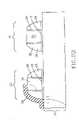
- FIG. 2Cillustrates the structure of FIG. 2B after a second stress liner 32 is formed thereon.
- the second stress liner 32covers a portion of the substrate 12 and the entire active gate region 16 as well as a portion of the dummy gate region 14 .
- the second stress liner 32extends atop a small segment of the patterned stress liner 30 such that an overlap 34 of the first and second stress liners is created atop the dummy gate region 14 .
- a compressive stress lineroverlaps a segment of the tensile stress liner atop the dummy gate region 14 .
- a tensile stress lineroverlaps a segment of a compressive stress liner. Additional embodiments have compressive stress liner and tensile stress liner in close proximity (within approximately 200 nm), but not directly overlapping.
- the dual stress liner boundary(surfaces of the stress liners that abut each other but do not overlap) is present atop the dummy gate region 14 as is shown in FIG. 2C .
- the large stress forces(represented by upper case ‘T’ for tensile, and by upper case “C” for compressive) generated by the dual stress liner boundary 36 are located within the dummy gate region 14 , not the substrate 12 as well the case with prior art dual stress liner technology.
- the dotted lines in the drawingagain refer to the zero stress lines.
- the second stress liner 32may be a tensile stress liner or a compressive stress liner with the proviso that it has opposite stress sign as compared to the first stress liner 30 .
- the second stress liner 32is a compressive stress liner. This configuration assumes that the active gate region 16 is pFET. A tensile stress liner would be used when the active device region 16 is an nFET.
- the presence of the second stress liner 32results in stress being introduced into the substrate 12 .
- the upper case ‘C’denotes the compressive stress induced by the presence of the second compressive stress liner on the substrate 12 .
- the dotted lines in the drawingagain refer to the zero stress lines.
- the second stress liner 32is formed utilizing the same basic processing steps as the first stress liner 30 . Hence, deposition, lithography and etching are used in forming the second stress liner 32 .
- the second stress lineris comprised of the same or different stress inducing materials as mentioned above for the first stress liner 30 .
- FIG. 3shows an alternative structure that can be formed by modifying the basic description provided above for FIGS. 2A-2C .
- the dummy gateis formed atop an isolation region 50 such as a trench isolation region.
- the isolation region 50is formed into the substrate 12 utilizing techniques that are well known to those skilled in the art.
- a trench isolation regioncan be formed by first providing a trench into the substrate by lithograpy and etching, the trench is then filled with a trench dielectric material, typically a trench oxide, and a planariziation process is then performed. It is noted that although this structure includes overlapped stress liners atop the dummy gate region, neither the invention nor this embodiment is limited to the same.
- the stress linersmay be perfectly abutted to each other over the dummy gate region (as shown in FIG. 4 ) or a gap 52 may be present between the stress liners atop the dummy gate region (as shown in FIG. 5 ).
- These alternative structurescan of course be used in conjugation with the embodiment depicted in FIGS. 2A-2C .
- the present inventionalso contemplates an embodiment wherein one of the stress liners is removed from the structure such that a single stress liner is present in which the single stress liner has an edge that lands atop the dummy gate region.
- a system in which a tensile stress liner is deposited but removed from a pFET; no compressive lineris used.
- the present inventionprovides a method and semiconductor structure that overcomes the dual stress liner boundary problem, without significantly increasing the overall size of the integrated circuit. This is achieved in the present invention by ensuring that the dual stress liner boundary between tensile and compressive stress liners is forced to land on a neighboring dummy gate region. By forcing the dual stress liner boundary to land on the dummy gate region, the large stresses associated with the dual stress liner boundary are transferred to the dummy gate region, not directly to the semiconductor substrate. Thus, the impact of the dual stress liner boundary on the nearest neighboring FET is reduced. Additionally, benefits of device variability and packing density are achieved utilizing the present invention.
Landscapes
- Metal-Oxide And Bipolar Metal-Oxide Semiconductor Integrated Circuits (AREA)
- Insulated Gate Type Field-Effect Transistor (AREA)
- Formation Of Insulating Films (AREA)
- Thin Film Transistor (AREA)
Abstract
Description
- The present invention relates to a semiconductor structure and a method of fabricating the same. More particularly, the present invention relates to a complementary metal oxide semiconductor (CMOS) structure that has improved device performance, which is obtained by using a modified dual stress liner technology. The present invention also provides a method of fabricating such a CMOS structure using the modified dual stress liner technology.
- For more than three decades, the continued miniaturization of silicon metal oxide semiconductor field effect transistors (MOSFETs) has driven the worldwide semiconductor industry. Various showstoppers to continued scaling have been predicated for decades, but a history of innovation has sustained Moore's Law in spite of many challenges. However, there are growing signs today that metal oxide semiconductor transistors are beginning to reach their traditional scaling limits.
- Since it has become increasingly difficult to improve MOSFETs and therefore CMOS performance through continued scaling, methods for improving performance without scaling have become critical. One approach for doing this is to increase carrier (electron and/or hole) mobilities. Increased carrier mobility can be obtained, for example, by introducing the appropriate stress/strain into the semiconductor lattice.
- The application of stress changes the lattice dimensions of the semiconductor substrate. By changing the lattice dimensions, the electronic band structure of the material is changed as well. This results in changes in carrier transport properties such as carrier scattering rates and effective mass, which can be dramatic in certain cases. The application of physical stress (tensile or compressive) can be further used to enhance the performance of devices fabricated on the semiconductor substrates.
- Compressive strain along the device channel increases drive current in p-type field effect transistors (pFETs) and decreases drive current in n-type field effect transistors (nFETs). Tensile strain along the device channel increases drive current in nFETs and decreases drive current in pFETs.
- Stress can be introduced into a single crystal oriented substrate by several methods including, for example, forming a stress liner on top of the substrate and around the gate region. Depending on the conductivity type of the FET (i.e., p or n), the stress liner is optimally under tensile stress (preferred for nFETs) or compressive stress (preferred for pFETs). When nFETs and pFETs are integrated onto the same semiconductor substrate, dual stress liner technology is typically used in which a first stress liner under tensile stress is formed around each nFET, while a second stress liner under compressive stress is formed around each pFET. It is noted that the order of forming the stress liners may be variable. For example, the compressive stress liner may be formed prior to the tensile stress liner or visa versa.
- However, the boundary between tensile and compressive stress liners in dual stress liner (DSL) technology also induces stress in the substrate, which can influence transistor performance as well. When the DSL boundary is in close proximity (with a lateral distance of about 5 microns or less) from an FET, and oriented parallel to the gate region, a degradation of the devices in proximity to the boundary has been observed. Degradation of 25% pFET and 18% nFET (saturation current at a fixed overdrive) have been demonstrated on recent CMOS structures, which is solely attributed to the DSL boundary influence mentioned above.
- Reference is now made to
FIGS. 1A-1D which illustrates the DSL boundary influence in greater detail for the case in which the tensile stress liner is formed prior to the formation of the compressive stress liner; in this case the compressive stress liner overlaps a portion of the tensile stress liner.FIG. 1A illustrates a portion of a non-stressedsemiconductor substrate 100 that has atensile stress liner 102 formed on a surface thereof. It is noted that no FET structures are shown inFIG. 1A since they lay to the periphery of the portion of thesubstrate 100 shown inFIG. 1A . The FETs are formed prior to disposing thetensile stress liner 102 on the substrate. FIG. 1B illustrates the structure ofFIG. 1A after patterning thetensile stress liner 102 by lithography and etching. As shown, anedge force 106 is created on thesubstrate 100. Moreover, thetensile stress liner 102 creates local stress in the substrate that decays with distance from the etched edge of theliner 102. InFIG. 1B ,reference numeral 108 denotes a region of thesubstrate 100 under compression, whilereference numeral 110 denotes a region of the substrate under tension. The dotted line (designated as112) denotes a zero stress line.FIG. 1C illustrates the structure ofFIG. 1B after forming acompressive stress liner 114 thereon. The overlap region (i.e., boundary)119 of the dual liners magnifies theedge force 106. Depending on the relative strengths of the tensile and compressive liners, the zero stress contour can take the form of112, or either of the two other contours indicated by112′.FIG. 1D is an expanded view ofFIG. 1C showing the presence of anFET 120 on a surface of thesubstrate 100. In this drawing, the substrate is under the following stresses (i) compression (c) under the FET120 (from left spacer outer edge to right spacer outer edge), (ii) tension (t) beneath thecompressive liner 114, and (iii) compression (c) under thetensile liner 102.- The problem with such a structure is that the dual
stress liner boundary 119 is in longitudinal proximity to theFET 120 which results in substantial degradation of the performance of the FET. The term “longitudinal proximity” is used in the present application to denote that the dualstress liner boundary 119 is located at a distance lengthwise from the FET that is about 5 microns or less. This degradation is observed for both nFETs and pFETs. In particular, it was been found that the longitudinal stress, which is related to the dualstress liner boundary 119, reduces the stress in the FET channel. - One solution to this dual stress liner boundary problem is to design an integrated circuit in which the longitudinal boundaries are placed far away (a longitudinal distance of greater than 5 microns) from the FET devices. Although such a solution is feasible, it does come with an area penalty that increases the overall size of the integrated circuit. Such an increase in size contradicts the current trend in shrinking integrated circuits.
- As such, a method is needed which overcomes the dual stress liner boundary problem without significantly increasing the overall size of the integrated circuit.
- The present invention provides a method and semiconductor structure that overcomes the dual stress liner boundary problem, without significantly increasing the overall size of the integrated circuit. In accordance with a first embodiment of the present invention, the dual stress liner boundary or gap is forced to land on a neighboring dummy gate region. By forcing the dual stress liner boundary or gap to land on the neighboring dummy gate region, the large stresses associated with the dual stress liner boundary are transferred to the dummy gate material, not the semiconductor substrate. The dummy gate region may be located within an active area of the FET or it may be present atop an isolation region such as a trench isolation region. Thus, the impact of the dual stress liner boundary on the nearest neighboring FET is reduced. Additionally, benefits of device variability and packing density are achieved utilizing the present invention.
- In general terms, the present invention provides, in a first embodiment, a semiconductor structure that includes:
- a semiconductor substrate having at least one dummy gate region in proximity to at least one active gate region; and
- a tensile stress liner and a compressive stress liner located on said substrate, wherein said tensile stress liner and said compressive stress liner are present at least in part over said at least one dummy gate region such that a boundary or gap that exits between the stress liners lands on top of said at least one dummy gate region.
- The at least one active gate region may comprise at least one pFET or at least one nFET. Combinations of nFETs and pFETs are also contemplated. In accordance with the presence invention, the boundary or gap between the compressive stress liner and the tensile stress liner is such that it falls atop a dummy gate region that is in close proximity to each FET present on the substrate.
- In accordance with the present invention, the compressive stress liner and the tensile stress liner may overlap each other, perfectly abut each other, or a gap may be present between the two liners. In accordance with the present invention the ‘boundary’ is created by the overlap or perfect abutment of the two stress liners, while the ‘gap’ is created by an underlap of the two stress liners.
- In one preferred embodiment of the present invention, the inventive structure comprises:
- a semiconductor substrate having at least one dummy gate region in proximity to at least one pFET; and
- a tensile stress liner and a compressive stress liner located on said substrate, wherein said compressive stress liner covers the at least one pFET and is present at least in part over said at least one dummy gate region such that a boundary or gap exists between the stress liners that lands on top of said at least one dummy gate region.
- In another preferred embodiment of the present invention, the inventive structure comprises:
- a semiconductor substrate having at least one dummy gate region in proximity to at least one nFET; and
- a tensile stress liner and a compressive stress liner located on said substrate, wherein said tensile stress liner covers the at least one nFET and is present at least in part over said at least one dummy gate region such that a boundary or gap exists between the stress liners that lands on top of said at least one dummy gate region.
- In addition to the semiconductor structure described above, the present invention also provides a method of fabricating the same. In general terms, the method of the present invention includes:
- providing a semiconductor substrate having at least one dummy gate region in proximity to at least one active gate region; and
- disposing, in any order, a tensile stress liner and a compressive stress liner on said substrate, wherein said tensile stress liner and said compressive stress liner are present at least in part over said at least one dummy gate region such that a boundary or gap between the stress liners lands on top of said at least one dummy gate region.
- In addition to using dual stress liners, the present application can also be applied to a semiconductor structure in which a single stress liner is present. In such an instance, the etched edge of the single stress liner is forced to land atop the dummy gate region of the structure.
FIGS. 1A-1D are pictorial representations (through cross sectional views) depicting prior art dual stress liner technology.FIGS. 2A-2C are pictorial representations (through cross sectional views) depicting the modified dual stress liner technology provided by the present invention.FIG. 3 is a pictorial representation (through a cross sectional view) depicting an alternative structure of the present application.FIG. 4 is a pictorial representation (through a cross sectional view) depicting another alternative structure of the present application.FIG. 5 is a pictorial representation (through a cross sectional view) depicting yet another alternative structure of the present application.- The present invention which provides a method and structure for improving device performance utilizing a variation in the conventional dual stress liner technology, will now be described in greater detail by referring to the following discussion and drawings that accompany the present application. It is noted that the drawings of the present application are provided for illustrative purposes and, as such, they are not drawn to scale.
- In the following description, numerous specific details are set forth, such as particular structures, components, materials, dimensions, processing steps and techniques, in order to provide a thorough understanding of the present invention. However, it will be appreciated by one of ordinary skill in the art that the invention may be practiced without these specific details. In other instances, well-known structures or processing steps have not been described in detail in order to avoid obscuring the invention.
- The present invention provides a method and structure in which a modified dual stress liner process is employed. The modified dual stress liner process of the present invention forces the dual stress liner boundary or gap to land on a dummy gate region that is in close proximity to an active gate region. By “dummy gate region”, it is meant a non-active gate region that is typically not a functional transistor, and is typically formed to minimize the variability of nearby active gates. The term “active gate region” denotes a functional transistor gate. By close proximity” it is meant that the boundary between the dual stress liners is from about 5 microns or less from the active gate region.
- Reference is first made to
FIG. 2A which illustrates aninitial structure 10 that is employed in the present invention. As shown, theinitial structure 10 includes asemiconductor substrate 12 having at least onedummy gate region 14 and at least oneactive gate region 16 in close proximity to each other. In accordance with the present invention, thedummy gate region 14 may be located atop an active region of the substrate as is shown in this drawing, or alternatively, the dummy gate may be located atop an isolation region present within or on the substrate. - The at least one
active gate region 16 may be an nFET or a pFET. Combinations of pFETs and nFETs are also contemplated in the present invention. - Each
dummy gate region 14 and eachactive gate 16 present on thesubstrate 12 includes agate dielectric 18 located on a surface of thesubstrate 12 and agate electrode 20 located on thegate dielectric 20. Eachactive gate region 16 includes a channel region (not shown) located within thesubstrate 12 and beneath the gate dielectric/gate electrode stack. Source/drain regions (not shown) are located adjacent to the channel region in each of the active gate regions. Eachdummy gate region 14 andactive gate region 16 may also include at least one sidewall spacer. InFIG. 1A , a pair of sidewall spacers including an inner L-shapedspacer 26 and anouter spacer 28 is shown. The at least one sidewall spacer is optional, and need not be used in all instances. - The at least one
dummy gate region 14 and the at least oneactive gate region 16 are fabricated using conventional complementary metal oxide semiconductor processing techniques well known to those skilled in the art. For example, deposition of various material layers, lithography, etching, ion implantation and annealing can be used in forming the active gate regions. The same processing steps can be used in forming the at least onedummy gate region 14. Each gate region (active and non-active) can also be formed utilizing a replacement gate process. - The
semiconductor substrate 12 includes any semiconductor material including, for example, Si, SiC, SiGeC, Ge, SiGe, Ga, GaAs, InAs, InP as well as other III/V or II/VI compound semiconductors. Layered semiconductors such as, for example, Si/SiGe and semiconductor-on-insulators (SOIs) are also contemplated herein. Typically, thesemiconductor substrate 12 is a Si-containing semiconductor such as, for example, Si, SiC, SiGe, SiGeC, or a silicon-on-insulator. Thesubstrate 12 may be unstrained, strained or include regions of strain and unstrain therein. Thesubstrate 12 may be intrinsic or it may be doped with, for example, but not limited to: B, As or P. - When SOI substrates are employed, those substrates include top and bottom semiconductor, e.g., Si, layers that are separated at least in part by a buried insulating layer. The buried insulating layer includes, for example, a crystalline or non-crystalline oxide, nitride or any combination thereof. Preferably, the buried insulating layer is an oxide. Typically, the buried insulating layer is formed during initial stages of a layer transfer process or during an ion implantation and annealing process, such as, for example, SIMOX (separation by ion implantation of oxygen).
- The
substrate 12 may have a single crystal orientation or alternatively hybrid semiconductor substrates having surface regions of different crystal orientations can also be employed. The hybrid substrate allows for fabricating a FET upon a specific crystal orientation that enhances the performance of each FET formed. For example, the hybrid substrate allows for providing a structure in which a pFET can be formed on a (110) crystal orientation, while the nFET can be formed on a (100) crystal orientation. When a hybrid substrate is used, it may have SOI-like properties, bulk-like properties or a combination of SOI- and bulk-like properties. - In some embodiments of the present invention, at least one isolation region (not shown) is formed into the
substrate 12. The at least one isolation region may include a trench isolation region, a field oxide isolation region or combinations thereof. The isolation regions are formed utilizing processing techniques well known to those skilled in the art. - The
gate dielectric 18 present in each of the gate regions can comprise the same or different insulating material. For example, thegate dielectric 18 can be comprised of an oxide, nitride, oxynitride, high k material (i.e., a dielectric material having a dielectric constant that is greater than silicon dioxide) or any combination thereof including multilayers. Preferably, thegate dielectric 18 is comprised of an oxide such as, for example, SiO2. - The
gate electrode 20 of each of the gate regions (active and dummy) can be comprised of the same or different conductive material, including, for example, polySi, SiGe, a metal, a metal alloy, a metal silicide, a metal nitride or combinations including multilayers thereof. When multilayers are present, a diffusion barrier (not shown), such as TiN or TaN, can be positioned between each of the conductive layers. A capping layer (also not shown), such as an oxide, or nitride, can be located atop the gate electrode of each of the gate regions the presence of the capping layer can be used to prevent subsequent formation of a silicide contact on said gate electrode. The silicide contact on said gate electrode is typically formed when the gate electrode includes a Si-containing material and no capping layer is present. Preferably, the gate electrode within each of the gate regions comprises polySi or polySiGe. - The at least one spacer that is optionally present is typically comprised of an oxide, nitride or oxynitride including combinations and multilayers thereof. Although optional, typically one spacer is present in the inventive structure. In the illustrated example, a pair of spacers is shown. Typically, the inner L-shaped
spacer 26 is comprised on an oxide, while theouter spacer 28 is comprised of a nitride. - As indicated above, each
active gate region 16 also includes S/D regions which typically include extension regions and deep S/D diffusion regions. The source/drain regions together with thegate electrode 20 define the length of the channel in theactive gate region 16. It is noted that S/D extensions and S/D diffusion regions are comprised of an upper portion of thesemiconductor substrate 12 that has been doped with either n- or p-type dopants by ion implantation. The S/D extensions are typically shallower in depth than the S/D diffusion regions. - Next, and as shown in
FIG. 2B , afirst stress liner 30 is formed on a portion of thesubstrate 12 as well as covering a portion of thedummy gate region 14. The terms “first and second stress liner” are used throughout this application to denote stress inducing materials that have been deposited and patterned by lithography and etching. In accordance with the method of the present invention, the first stress liner may be a tensile stress liner or a compressive stress liner. In a preferred embodiment, and for the drawings illustrated in the present application, thefirst stress liner 30 is a tensile stress liner. This configuration assumes that theactive gate region 16 is a pFET. A compressive stress liner would be used for thefirst stress liner 30 when theactive gate region 16 is an nFET. - The presence of the stress liner results in stresses being introduced into the
substrate 12. In the drawing, the lower case ‘t’ denotes the tensile stress induced into the substrate by the presence of the tensile stress liner, while the lower case ‘c’ denotes the compressive stress induced by the presence of the tensile stress liner on thesubstrate 12. The dotted lines represent the zero stress lines present in the substrate. It is noted that when thefirst stress liner 30 is a compressive stress liner, the position of the lower case c and t would be reversed from that shown inFIG. 2B . - The
first stress liner 30 is comprised of any stress inducing material such as a nitride or a high density plasma (HDP) oxide, or a combination thereof. The stress liner can formed by various chemical vapor deposition (CVD) processes such as low pressure CVD (LPCVD), plasma enhanced CVD (PECVD), rapid thermal CVD (RTCVD) or BTBAS-based (C8H22N2Si reacted with ammonia) CVD, where BTBAS is a modern metalorganic precursor for CVD application. The later process provides a low temperature nitride film having high stress. Following deposition of the stress liner material, lithography and etching are used in forming thefirst stress liner 30. - Preferably, the
first stress liner 30 comprises a nitride, such as Si3N4, wherein the process conditions of the deposition process are selected to provide an intrinsic tensile strain within the deposited layer. For example, plasma enhanced chemical vapor deposition (PECVD) can provide nitride stress liners having an intrinsic tensile strain. The stress state (tensile or compressive) of the stress liners deposited by PECVD can be controlled by changing the deposition conditions to alter the reaction rate within the deposition chamber. More specifically, the stress state of a deposited nitride stress liner may be set by changing the deposition conditions such as: SiH4/N2/He gas flow rate, pressure, RF power, and electrode gap. - In another example, rapid thermal chemical vapor deposition (RTCVD) can provide nitride tensile stress liners having an internal tensile strain. The magnitude of the internal tensile strain produced within the nitride tensile stress liner deposited by RTCVD can be controlled by changing the deposition conditions. More specifically, the magnitude of the tensile strain within the nitride stress liner may be set by changing deposition conditions such as: precursor composition, precursor flow rate and temperature.
FIG. 2C illustrates the structure ofFIG. 2B after asecond stress liner 32 is formed thereon. In accordance with the present invention, thesecond stress liner 32 covers a portion of thesubstrate 12 and the entireactive gate region 16 as well as a portion of thedummy gate region 14. As shown, thesecond stress liner 32 extends atop a small segment of the patternedstress liner 30 such that anoverlap 34 of the first and second stress liners is created atop thedummy gate region 14. In one embodiment, a compressive stress liner overlaps a segment of the tensile stress liner atop thedummy gate region 14. In another embodiment, a tensile stress liner overlaps a segment of a compressive stress liner. Additional embodiments have compressive stress liner and tensile stress liner in close proximity (within approximately 200 nm), but not directly overlapping.- Due to the location of the
overlap 34, the dual stress liner boundary (surfaces of the stress liners that abut each other but do not overlap) is present atop thedummy gate region 14 as is shown inFIG. 2C . The large stress forces (represented by upper case ‘T’ for tensile, and by upper case “C” for compressive) generated by the dualstress liner boundary 36 are located within thedummy gate region 14, not thesubstrate 12 as well the case with prior art dual stress liner technology. The dotted lines in the drawing again refer to the zero stress lines. - In accordance with the method of the present invention, the
second stress liner 32 may be a tensile stress liner or a compressive stress liner with the proviso that it has opposite stress sign as compared to thefirst stress liner 30. In a preferred embodiment, and for the drawings illustrated in the present application, thesecond stress liner 32 is a compressive stress liner. This configuration assumes that theactive gate region 16 is pFET. A tensile stress liner would be used when theactive device region 16 is an nFET. - The presence of the
second stress liner 32 results in stress being introduced into thesubstrate 12. In the drawing, the upper case ‘C’ denotes the compressive stress induced by the presence of the second compressive stress liner on thesubstrate 12. The dotted lines in the drawing again refer to the zero stress lines. - The
second stress liner 32 is formed utilizing the same basic processing steps as thefirst stress liner 30. Hence, deposition, lithography and etching are used in forming thesecond stress liner 32. The second stress liner is comprised of the same or different stress inducing materials as mentioned above for thefirst stress liner 30. FIG. 3 shows an alternative structure that can be formed by modifying the basic description provided above forFIGS. 2A-2C . In the structure illustrated inFIG. 3 the dummy gate is formed atop anisolation region 50 such as a trench isolation region. Theisolation region 50 is formed into thesubstrate 12 utilizing techniques that are well known to those skilled in the art. For example, a trench isolation region can be formed by first providing a trench into the substrate by lithograpy and etching, the trench is then filled with a trench dielectric material, typically a trench oxide, and a planariziation process is then performed. It is noted that although this structure includes overlapped stress liners atop the dummy gate region, neither the invention nor this embodiment is limited to the same. Instead, the stress liners may be perfectly abutted to each other over the dummy gate region (as shown inFIG. 4 ) or agap 52 may be present between the stress liners atop the dummy gate region (as shown inFIG. 5 ). These alternative structures can of course be used in conjugation with the embodiment depicted inFIGS. 2A-2C .- In addition to the above embodiments and alternative structures, the present invention also contemplates an embodiment wherein one of the stress liners is removed from the structure such that a single stress liner is present in which the single stress liner has an edge that lands atop the dummy gate region. For example, a system in which a tensile stress liner is deposited but removed from a pFET; no compressive liner is used.
- As indicated above, the present invention provides a method and semiconductor structure that overcomes the dual stress liner boundary problem, without significantly increasing the overall size of the integrated circuit. This is achieved in the present invention by ensuring that the dual stress liner boundary between tensile and compressive stress liners is forced to land on a neighboring dummy gate region. By forcing the dual stress liner boundary to land on the dummy gate region, the large stresses associated with the dual stress liner boundary are transferred to the dummy gate region, not directly to the semiconductor substrate. Thus, the impact of the dual stress liner boundary on the nearest neighboring FET is reduced. Additionally, benefits of device variability and packing density are achieved utilizing the present invention.
- While the present invention has been particularly shown and described with respect to preferred embodiments thereof, it will be understood by those skilled in the art that the foregoing and other changes in forms and details may be made without departing from the spirit and scope of the present invention. It is therefore intended that the present invention not be limited to the exact forms and details described and illustrated, but fall within the scope of the appended claims.
Claims (28)
Priority Applications (5)
| Application Number | Priority Date | Filing Date | Title |
|---|---|---|---|
| US11/468,402US7462522B2 (en) | 2006-08-30 | 2006-08-30 | Method and structure for improving device performance variation in dual stress liner technology |
| JP2009526029AJP5220749B2 (en) | 2006-08-30 | 2007-08-09 | Method and structure for improving device performance variability in dual stress liner technology |
| PCT/EP2007/058273WO2008025661A1 (en) | 2006-08-30 | 2007-08-09 | Method and structure for improving device performance variation in dual stress liner technology |
| TW096131630ATW200830552A (en) | 2006-08-30 | 2007-08-27 | Method and structure for improving device performance variation in dual stress liner technology |
| US12/328,358US7843024B2 (en) | 2006-08-30 | 2008-12-04 | Method and structure for improving device performance variation in dual stress liner technology |
Applications Claiming Priority (1)
| Application Number | Priority Date | Filing Date | Title |
|---|---|---|---|
| US11/468,402US7462522B2 (en) | 2006-08-30 | 2006-08-30 | Method and structure for improving device performance variation in dual stress liner technology |
Related Child Applications (1)
| Application Number | Title | Priority Date | Filing Date |
|---|---|---|---|
| US12/328,358ContinuationUS7843024B2 (en) | 2006-08-30 | 2008-12-04 | Method and structure for improving device performance variation in dual stress liner technology |
Publications (2)
| Publication Number | Publication Date |
|---|---|
| US20080057653A1true US20080057653A1 (en) | 2008-03-06 |
| US7462522B2 US7462522B2 (en) | 2008-12-09 |
Family
ID=38669778
Family Applications (2)
| Application Number | Title | Priority Date | Filing Date |
|---|---|---|---|
| US11/468,402Expired - Fee RelatedUS7462522B2 (en) | 2006-08-30 | 2006-08-30 | Method and structure for improving device performance variation in dual stress liner technology |
| US12/328,358Active2027-02-11US7843024B2 (en) | 2006-08-30 | 2008-12-04 | Method and structure for improving device performance variation in dual stress liner technology |
Family Applications After (1)
| Application Number | Title | Priority Date | Filing Date |
|---|---|---|---|
| US12/328,358Active2027-02-11US7843024B2 (en) | 2006-08-30 | 2008-12-04 | Method and structure for improving device performance variation in dual stress liner technology |
Country Status (4)
| Country | Link |
|---|---|
| US (2) | US7462522B2 (en) |
| JP (1) | JP5220749B2 (en) |
| TW (1) | TW200830552A (en) |
| WO (1) | WO2008025661A1 (en) |
Cited By (3)
| Publication number | Priority date | Publication date | Assignee | Title |
|---|---|---|---|---|
| US20070032009A1 (en)* | 2002-06-07 | 2007-02-08 | Amberwave Systems Corporation | Semiconductor devices having strained dual channel layers |
| US20100193870A1 (en)* | 2009-01-30 | 2010-08-05 | Xilinx, Inc. | Techniques for improving transistor-to-transistor stress uniformity |
| CN102891109A (en)* | 2011-07-18 | 2013-01-23 | 中芯国际集成电路制造(上海)有限公司 | Semiconductor device forming method |
Families Citing this family (15)
| Publication number | Priority date | Publication date | Assignee | Title |
|---|---|---|---|---|
| US7301180B2 (en) | 2001-06-18 | 2007-11-27 | Massachusetts Institute Of Technology | Structure and method for a high-speed semiconductor device having a Ge channel layer |
| US7462522B2 (en)* | 2006-08-30 | 2008-12-09 | International Business Machines Corporation | Method and structure for improving device performance variation in dual stress liner technology |
| US7601574B2 (en)* | 2006-10-25 | 2009-10-13 | Globalfoundries Inc. | Methods for fabricating a stress enhanced MOS transistor |
| KR100825809B1 (en)* | 2007-02-27 | 2008-04-29 | 삼성전자주식회사 | Structure of semiconductor device having strain layer and manufacturing method thereof |
| US7761838B2 (en)* | 2007-09-26 | 2010-07-20 | Globalfoundries Inc. | Method for fabricating a semiconductor device having an extended stress liner |
| US8039897B2 (en)* | 2008-12-19 | 2011-10-18 | Fairchild Semiconductor Corporation | Lateral MOSFET with substrate drain connection |
| US8638594B1 (en)* | 2009-12-02 | 2014-01-28 | Altera Corporation | Integrated circuits with asymmetric transistors |
| US8467233B2 (en)* | 2011-06-06 | 2013-06-18 | Texas Instruments Incorporated | Asymmetric static random access memory cell with dual stress liner |
| US8466513B2 (en) | 2011-06-13 | 2013-06-18 | Semiconductor Components Industries, Llc | Semiconductor device with enhanced mobility and method |
| US8779838B2 (en) | 2011-10-25 | 2014-07-15 | International Business Machines Corporation | Methodology and apparatus for tuning driving current of semiconductor transistors |
| US8492218B1 (en) | 2012-04-03 | 2013-07-23 | International Business Machines Corporation | Removal of an overlap of dual stress liners |
| US8778764B2 (en) | 2012-07-16 | 2014-07-15 | Semiconductor Components Industries, Llc | Method of making an insulated gate semiconductor device having a shield electrode structure and structure therefor |
| US9209174B2 (en)* | 2013-02-15 | 2015-12-08 | Globalfoundries Inc. | Circuit element including a layer of a stress-creating material providing a variable stress and method for the formation thereof |
| US9269779B2 (en) | 2014-07-21 | 2016-02-23 | Semiconductor Components Industries, Llc | Insulated gate semiconductor device having a shield electrode structure |
| KR102320820B1 (en) | 2015-02-24 | 2021-11-02 | 삼성전자주식회사 | Integrated circuit device and method of manufacturing the same |
Citations (79)
| Publication number | Priority date | Publication date | Assignee | Title |
|---|---|---|---|---|
| US3602841A (en)* | 1970-06-18 | 1971-08-31 | Ibm | High frequency bulk semiconductor amplifiers and oscillators |
| US4665415A (en)* | 1985-04-24 | 1987-05-12 | International Business Machines Corporation | Semiconductor device with hole conduction via strained lattice |
| US4853076A (en)* | 1983-12-29 | 1989-08-01 | Massachusetts Institute Of Technology | Semiconductor thin films |
| US4855245A (en)* | 1985-09-13 | 1989-08-08 | Siemens Aktiengesellschaft | Method of manufacturing integrated circuit containing bipolar and complementary MOS transistors on a common substrate |
| US4952524A (en)* | 1989-05-05 | 1990-08-28 | At&T Bell Laboratories | Semiconductor device manufacture including trench formation |
| US4958213A (en)* | 1987-12-07 | 1990-09-18 | Texas Instruments Incorporated | Method for forming a transistor base region under thick oxide |
| US5006913A (en)* | 1988-11-05 | 1991-04-09 | Mitsubishi Denki Kabushiki Kaisha | Stacked type semiconductor device |
| US5060030A (en)* | 1990-07-18 | 1991-10-22 | Raytheon Company | Pseudomorphic HEMT having strained compensation layer |
| US5081513A (en)* | 1991-02-28 | 1992-01-14 | Xerox Corporation | Electronic device with recovery layer proximate to active layer |
| US5108843A (en)* | 1988-11-30 | 1992-04-28 | Ricoh Company, Ltd. | Thin film semiconductor and process for producing the same |
| US5134085A (en)* | 1991-11-21 | 1992-07-28 | Micron Technology, Inc. | Reduced-mask, split-polysilicon CMOS process, incorporating stacked-capacitor cells, for fabricating multi-megabit dynamic random access memories |
| US5310446A (en)* | 1990-01-10 | 1994-05-10 | Ricoh Company, Ltd. | Method for producing semiconductor film |
| US5354695A (en)* | 1992-04-08 | 1994-10-11 | Leedy Glenn J | Membrane dielectric isolation IC fabrication |
| US5391510A (en)* | 1992-02-28 | 1995-02-21 | International Business Machines Corporation | Formation of self-aligned metal gate FETs using a benignant removable gate material during high temperature steps |
| US5459346A (en)* | 1988-06-28 | 1995-10-17 | Ricoh Co., Ltd. | Semiconductor substrate with electrical contact in groove |
| US5557122A (en)* | 1995-05-12 | 1996-09-17 | Alliance Semiconductors Corporation | Semiconductor electrode having improved grain structure and oxide growth properties |
| US5561302A (en)* | 1994-09-26 | 1996-10-01 | Motorola, Inc. | Enhanced mobility MOSFET device and method |
| US5670798A (en)* | 1995-03-29 | 1997-09-23 | North Carolina State University | Integrated heterostructures of Group III-V nitride semiconductor materials including epitaxial ohmic contact non-nitride buffer layer and methods of fabricating same |
| US5861651A (en)* | 1997-02-28 | 1999-01-19 | Lucent Technologies Inc. | Field effect devices and capacitors with improved thin film dielectrics and method for making same |
| US5880040A (en)* | 1996-04-15 | 1999-03-09 | Macronix International Co., Ltd. | Gate dielectric based on oxynitride grown in N2 O and annealed in NO |
| US5940736A (en)* | 1997-03-11 | 1999-08-17 | Lucent Technologies Inc. | Method for forming a high quality ultrathin gate oxide layer |
| US5940716A (en)* | 1996-03-15 | 1999-08-17 | Samsung Electronics Co., Ltd. | Methods of forming trench isolation regions using repatterned trench masks |
| US5960297A (en)* | 1997-07-02 | 1999-09-28 | Kabushiki Kaisha Toshiba | Shallow trench isolation structure and method of forming the same |
| US6025280A (en)* | 1997-04-28 | 2000-02-15 | Lucent Technologies Inc. | Use of SiD4 for deposition of ultra thin and controllable oxides |
| US6066545A (en)* | 1997-12-09 | 2000-05-23 | Texas Instruments Incorporated | Birdsbeak encroachment using combination of wet and dry etch for isolation nitride |
| US6090684A (en)* | 1998-07-31 | 2000-07-18 | Hitachi, Ltd. | Method for manufacturing semiconductor device |
| US6107143A (en)* | 1998-03-02 | 2000-08-22 | Samsung Electronics Co., Ltd. | Method for forming a trench isolation structure in an integrated circuit |
| US6117722A (en)* | 1999-02-18 | 2000-09-12 | Taiwan Semiconductor Manufacturing Company | SRAM layout for relaxing mechanical stress in shallow trench isolation technology and method of manufacture thereof |
| US6221735B1 (en)* | 2000-02-15 | 2001-04-24 | Philips Semiconductors, Inc. | Method for eliminating stress induced dislocations in CMOS devices |
| US6228694B1 (en)* | 1999-06-28 | 2001-05-08 | Intel Corporation | Method of increasing the mobility of MOS transistors by use of localized stress regions |
| US6255169B1 (en)* | 1999-02-22 | 2001-07-03 | Advanced Micro Devices, Inc. | Process for fabricating a high-endurance non-volatile memory device |
| US6261964B1 (en)* | 1997-03-14 | 2001-07-17 | Micron Technology, Inc. | Material removal method for forming a structure |
| US6265317B1 (en)* | 2001-01-09 | 2001-07-24 | Taiwan Semiconductor Manufacturing Company | Top corner rounding for shallow trench isolation |
| US20010009784A1 (en)* | 1998-01-09 | 2001-07-26 | Yanjun Ma | Structure and method of making a sub-micron MOS transistor |
| US6274444B1 (en)* | 1999-07-30 | 2001-08-14 | United Microelectronics Corp. | Method for forming mosfet |
| US6281532B1 (en)* | 1999-06-28 | 2001-08-28 | Intel Corporation | Technique to obtain increased channel mobilities in NMOS transistors by gate electrode engineering |
| US6284623B1 (en)* | 1999-10-25 | 2001-09-04 | Peng-Fei Zhang | Method of fabricating semiconductor devices using shallow trench isolation with reduced narrow channel effect |
| US6284626B1 (en)* | 1999-04-06 | 2001-09-04 | Vantis Corporation | Angled nitrogen ion implantation for minimizing mechanical stress on side walls of an isolation trench |
| US6361885B1 (en)* | 1998-04-10 | 2002-03-26 | Organic Display Technology | Organic electroluminescent materials and device made from such materials |
| US6362082B1 (en)* | 1999-06-28 | 2002-03-26 | Intel Corporation | Methodology for control of short channel effects in MOS transistors |
| US6368931B1 (en)* | 2000-03-27 | 2002-04-09 | Intel Corporation | Thin tensile layers in shallow trench isolation and method of making same |
| US20020063292A1 (en)* | 2000-11-29 | 2002-05-30 | Mark Armstrong | CMOS fabrication process utilizing special transistor orientation |
| US6403486B1 (en)* | 2001-04-30 | 2002-06-11 | Taiwan Semiconductor Manufacturing Company | Method for forming a shallow trench isolation |
| US6403975B1 (en)* | 1996-04-09 | 2002-06-11 | Max-Planck Gesellschaft Zur Forderung Der Wissenschafteneev | Semiconductor components, in particular photodetectors, light emitting diodes, optical modulators and waveguides with multilayer structures grown on silicon substrates |
| US6406973B1 (en)* | 1999-06-29 | 2002-06-18 | Hyundai Electronics Industries Co., Ltd. | Transistor in a semiconductor device and method of manufacturing the same |
| US20020086497A1 (en)* | 2000-12-30 | 2002-07-04 | Kwok Siang Ping | Beaker shape trench with nitride pull-back for STI |
| US20020086472A1 (en)* | 2000-12-29 | 2002-07-04 | Brian Roberds | Technique to obtain high mobility channels in MOS transistors by forming a strain layer on an underside of a channel |
| US20020090791A1 (en)* | 1999-06-28 | 2002-07-11 | Brian S. Doyle | Method for reduced capacitance interconnect system using gaseous implants into the ild |
| US6506652B2 (en)* | 1998-11-13 | 2003-01-14 | Intel Corporation | Method of recessing spacers to improved salicide resistance on polysilicon gates |
| US20030013259A1 (en)* | 2001-07-13 | 2003-01-16 | International Business Machines Corporation | Reduction of polysilicon stress in trench capacitors |
| US20030032261A1 (en)* | 2001-08-08 | 2003-02-13 | Ling-Yen Yeh | Method of preventing threshold voltage of MOS transistor from being decreased by shallow trench isolation formation |
| US20030040158A1 (en)* | 2001-08-21 | 2003-02-27 | Nec Corporation | Semiconductor device and method of fabricating the same |
| US6531369B1 (en)* | 2000-03-01 | 2003-03-11 | Applied Micro Circuits Corporation | Heterojunction bipolar transistor (HBT) fabrication using a selectively deposited silicon germanium (SiGe) |
| US6531740B2 (en)* | 2001-07-17 | 2003-03-11 | Motorola, Inc. | Integrated impedance matching and stability network |
| US20030057184A1 (en)* | 2001-09-22 | 2003-03-27 | Shiuh-Sheng Yu | Method for pull back SiN to increase rounding effect in a shallow trench isolation process |
| US20030067035A1 (en)* | 2001-09-28 | 2003-04-10 | Helmut Tews | Gate processing method with reduced gate oxide corner and edge thinning |
| US6621392B1 (en)* | 2002-04-25 | 2003-09-16 | International Business Machines Corporation | Micro electromechanical switch having self-aligned spacers |
| US20040029323A1 (en)* | 2000-11-22 | 2004-02-12 | Akihiro Shimizu | Semiconductor device and method for fabricating the same |
| US6717216B1 (en)* | 2002-12-12 | 2004-04-06 | International Business Machines Corporation | SOI based field effect transistor having a compressive film in undercut area under the channel and a method of making the device |
| US20040113174A1 (en)* | 2002-12-12 | 2004-06-17 | International Business Machines Corporation | Isolation structures for imposing stress patterns |
| US20040113217A1 (en)* | 2002-12-12 | 2004-06-17 | International Business Machines Corporation | Stress inducing spacers |
| US20050054148A1 (en)* | 2003-09-10 | 2005-03-10 | International Business Machines Corporation | METHOD AND STRUCTURE FOR IMPROVED MOSFETs USING POLY/SILICIDE GATE HEIGHT CONTROL |
| US20050059201A1 (en)* | 2003-09-12 | 2005-03-17 | International Business Machines Corporation | Mosfet performance improvement using deformation in soi structure |
| US6869866B1 (en)* | 2003-09-22 | 2005-03-22 | International Business Machines Corporation | Silicide proximity structures for CMOS device performance improvements |
| US20050064646A1 (en)* | 2003-09-23 | 2005-03-24 | Dureseti Chidambarrao | NFETs using gate induced stress modulation |
| US20050082616A1 (en)* | 2003-10-20 | 2005-04-21 | Huajie Chen | High performance stress-enhanced MOSFETs using Si:C and SiGe epitaxial source/drain and method of manufacture |
| US20050085022A1 (en)* | 2003-10-20 | 2005-04-21 | Dureseti Chidambarrao | Strained dislocation-free channels for CMOS and method of manufacture |
| US20050082634A1 (en)* | 2003-10-16 | 2005-04-21 | International Business Machines Corporation | High performance strained cmos devices |
| US20050093059A1 (en)* | 2003-10-30 | 2005-05-05 | Belyansky Michael P. | Structure and method to improve channel mobility by gate electrode stress modification |
| US20050093030A1 (en)* | 2003-10-30 | 2005-05-05 | Doris Bruce B. | Structure and method to enhance both nFET and pFET performance using different kinds of stressed layers |
| US20050098829A1 (en)* | 2003-11-06 | 2005-05-12 | Doris Bruce B. | High mobility CMOS circuits |
| US20050104131A1 (en)* | 2003-11-19 | 2005-05-19 | Dureseti Chidambarrao | Silicon device on Si:C-OI and SGOI and method of manufacture |
| US20050106799A1 (en)* | 2003-11-14 | 2005-05-19 | International Business Machines Corporation | Stressed semiconductor device structures having granular semiconductor material |
| US20050130358A1 (en)* | 2003-12-12 | 2005-06-16 | Dureseti Chidambarrao | Strained finFETs and method of manufacture |
| US20050145954A1 (en)* | 2004-01-05 | 2005-07-07 | International Business Machines Corporation | Structures and methods for making strained mosfets |
| US20050194699A1 (en)* | 2004-03-03 | 2005-09-08 | International Business Machines Corporation | Mobility enhanced cmos devices |
| US20060057787A1 (en)* | 2002-11-25 | 2006-03-16 | Doris Bruce B | Strained finfet cmos device structures |
| US20060060925A1 (en)* | 2004-09-17 | 2006-03-23 | International Business Machines Corporation | Semiconductor device structure with active regions having different surface directions and methods |
| US7052946B2 (en)* | 2004-03-10 | 2006-05-30 | Taiwan Semiconductor Manufacturing Co. Ltd. | Method for selectively stressing MOSFETs to improve charge carrier mobility |
Family Cites Families (33)
| Publication number | Priority date | Publication date | Assignee | Title |
|---|---|---|---|---|
| JPS6476755A (en) | 1987-09-18 | 1989-03-22 | Hitachi Ltd | Semiconductor device |
| US5371399A (en) | 1991-06-14 | 1994-12-06 | International Business Machines Corporation | Compound semiconductor having metallic inclusions and devices fabricated therefrom |
| US6008126A (en) | 1992-04-08 | 1999-12-28 | Elm Technology Corporation | Membrane dielectric isolation IC fabrication |
| US5679965A (en) | 1995-03-29 | 1997-10-21 | North Carolina State University | Integrated heterostructures of Group III-V nitride semiconductor materials including epitaxial ohmic contact, non-nitride buffer layer and methods of fabricating same |
| JP3139426B2 (en) | 1997-10-15 | 2001-02-26 | 日本電気株式会社 | Semiconductor device |
| US6165383A (en) | 1998-04-10 | 2000-12-26 | Organic Display Technology | Useful precursors for organic electroluminescent materials and devices made from such materials |
| US5989978A (en) | 1998-07-16 | 1999-11-23 | Chartered Semiconductor Manufacturing, Ltd. | Shallow trench isolation of MOSFETS with reduced corner parasitic currents |
| US6319794B1 (en) | 1998-10-14 | 2001-11-20 | International Business Machines Corporation | Structure and method for producing low leakage isolation devices |
| US6483171B1 (en) | 1999-08-13 | 2002-11-19 | Micron Technology, Inc. | Vertical sub-micron CMOS transistors on (110), (111), (311), (511), and higher order surfaces of bulk, SOI and thin film structures and method of forming same |
| JP3506645B2 (en) | 1999-12-13 | 2004-03-15 | Necエレクトロニクス株式会社 | Semiconductor device and manufacturing method thereof |
| US6476462B2 (en) | 1999-12-28 | 2002-11-05 | Texas Instruments Incorporated | MOS-type semiconductor device and method for making same |
| US6493497B1 (en) | 2000-09-26 | 2002-12-10 | Motorola, Inc. | Electro-optic structure and process for fabricating same |
| US6501121B1 (en) | 2000-11-15 | 2002-12-31 | Motorola, Inc. | Semiconductor structure |
| US6498358B1 (en) | 2001-07-20 | 2002-12-24 | Motorola, Inc. | Structure and method for fabricating an electro-optic system having an electrochromic diffraction grating |
| US6831292B2 (en) | 2001-09-21 | 2004-12-14 | Amberwave Systems Corporation | Semiconductor structures employing strained material layers with defined impurity gradients and methods for fabricating same |
| US6635506B2 (en) | 2001-11-07 | 2003-10-21 | International Business Machines Corporation | Method of fabricating micro-electromechanical switches on CMOS compatible substrates |
| US6461936B1 (en) | 2002-01-04 | 2002-10-08 | Infineon Technologies Ag | Double pullback method of filling an isolation trench |
| JP2004014954A (en)* | 2002-06-11 | 2004-01-15 | Hitachi Ltd | Semiconductor device |
| US6887798B2 (en) | 2003-05-30 | 2005-05-03 | International Business Machines Corporation | STI stress modification by nitrogen plasma treatment for improving performance in small width devices |
| US7279746B2 (en) | 2003-06-30 | 2007-10-09 | International Business Machines Corporation | High performance CMOS device structures and method of manufacture |
| US7504693B2 (en) | 2004-04-23 | 2009-03-17 | International Business Machines Corporation | Dislocation free stressed channels in bulk silicon and SOI CMOS devices by gate stress engineering |
| US7002209B2 (en) | 2004-05-21 | 2006-02-21 | International Business Machines Corporation | MOSFET structure with high mechanical stress in the channel |
| US7361973B2 (en) | 2004-05-21 | 2008-04-22 | International Business Machines Corporation | Embedded stressed nitride liners for CMOS performance improvement |
| US7223994B2 (en) | 2004-06-03 | 2007-05-29 | International Business Machines Corporation | Strained Si on multiple materials for bulk or SOI substrates |
| JP4994581B2 (en) | 2004-06-29 | 2012-08-08 | 富士通セミコンダクター株式会社 | Semiconductor device |
| DE102004042167B4 (en) | 2004-08-31 | 2009-04-02 | Advanced Micro Devices, Inc., Sunnyvale | A method of forming a semiconductor structure comprising transistor elements having differently strained channel regions, and corresponding semiconductor structure |
| DE102004052617B4 (en) | 2004-10-29 | 2010-08-05 | Advanced Micro Devices, Inc., Sunnyvale | A method of manufacturing a semiconductor device and semiconductor device having semiconductor regions having differently deformed channel regions |
| JP5002891B2 (en)* | 2004-12-17 | 2012-08-15 | 富士通セミコンダクター株式会社 | Manufacturing method of semiconductor device |
| JP4760414B2 (en)* | 2006-02-06 | 2011-08-31 | ソニー株式会社 | Manufacturing method of semiconductor device |
| US7592653B2 (en)* | 2006-04-24 | 2009-09-22 | Toshiba America Electronic Components, Inc. | Stress relaxation for top of transistor gate |
| US7521307B2 (en) | 2006-04-28 | 2009-04-21 | International Business Machines Corporation | CMOS structures and methods using self-aligned dual stressed layers |
| US7585720B2 (en)* | 2006-07-05 | 2009-09-08 | Toshiba America Electronic Components, Inc. | Dual stress liner device and method |
| US7462522B2 (en)* | 2006-08-30 | 2008-12-09 | International Business Machines Corporation | Method and structure for improving device performance variation in dual stress liner technology |
- 2006
- 2006-08-30USUS11/468,402patent/US7462522B2/ennot_activeExpired - Fee Related
- 2007
- 2007-08-09JPJP2009526029Apatent/JP5220749B2/ennot_activeExpired - Fee Related
- 2007-08-09WOPCT/EP2007/058273patent/WO2008025661A1/enactiveApplication Filing
- 2007-08-27TWTW096131630Apatent/TW200830552A/enunknown
- 2008
- 2008-12-04USUS12/328,358patent/US7843024B2/enactiveActive
Patent Citations (99)
| Publication number | Priority date | Publication date | Assignee | Title |
|---|---|---|---|---|
| US3602841A (en)* | 1970-06-18 | 1971-08-31 | Ibm | High frequency bulk semiconductor amplifiers and oscillators |
| US4853076A (en)* | 1983-12-29 | 1989-08-01 | Massachusetts Institute Of Technology | Semiconductor thin films |
| US4665415A (en)* | 1985-04-24 | 1987-05-12 | International Business Machines Corporation | Semiconductor device with hole conduction via strained lattice |
| US4855245A (en)* | 1985-09-13 | 1989-08-08 | Siemens Aktiengesellschaft | Method of manufacturing integrated circuit containing bipolar and complementary MOS transistors on a common substrate |
| US4958213A (en)* | 1987-12-07 | 1990-09-18 | Texas Instruments Incorporated | Method for forming a transistor base region under thick oxide |
| US5565697A (en)* | 1988-06-28 | 1996-10-15 | Ricoh Company, Ltd. | Semiconductor structure having island forming grooves |
| US5459346A (en)* | 1988-06-28 | 1995-10-17 | Ricoh Co., Ltd. | Semiconductor substrate with electrical contact in groove |
| US5006913A (en)* | 1988-11-05 | 1991-04-09 | Mitsubishi Denki Kabushiki Kaisha | Stacked type semiconductor device |
| US5108843A (en)* | 1988-11-30 | 1992-04-28 | Ricoh Company, Ltd. | Thin film semiconductor and process for producing the same |
| US4952524A (en)* | 1989-05-05 | 1990-08-28 | At&T Bell Laboratories | Semiconductor device manufacture including trench formation |
| US5310446A (en)* | 1990-01-10 | 1994-05-10 | Ricoh Company, Ltd. | Method for producing semiconductor film |
| US5060030A (en)* | 1990-07-18 | 1991-10-22 | Raytheon Company | Pseudomorphic HEMT having strained compensation layer |
| US5081513A (en)* | 1991-02-28 | 1992-01-14 | Xerox Corporation | Electronic device with recovery layer proximate to active layer |
| US5134085A (en)* | 1991-11-21 | 1992-07-28 | Micron Technology, Inc. | Reduced-mask, split-polysilicon CMOS process, incorporating stacked-capacitor cells, for fabricating multi-megabit dynamic random access memories |
| US5391510A (en)* | 1992-02-28 | 1995-02-21 | International Business Machines Corporation | Formation of self-aligned metal gate FETs using a benignant removable gate material during high temperature steps |
| US5354695A (en)* | 1992-04-08 | 1994-10-11 | Leedy Glenn J | Membrane dielectric isolation IC fabrication |
| US5946559A (en)* | 1992-04-08 | 1999-08-31 | Elm Technology Corporation | Membrane dielectric isolation IC fabrication |
| US5592018A (en)* | 1992-04-08 | 1997-01-07 | Leedy; Glenn J. | Membrane dielectric isolation IC fabrication |
| US5592007A (en)* | 1992-04-08 | 1997-01-07 | Leedy; Glenn J. | Membrane dielectric isolation transistor fabrication |
| US5561302A (en)* | 1994-09-26 | 1996-10-01 | Motorola, Inc. | Enhanced mobility MOSFET device and method |
| US5670798A (en)* | 1995-03-29 | 1997-09-23 | North Carolina State University | Integrated heterostructures of Group III-V nitride semiconductor materials including epitaxial ohmic contact non-nitride buffer layer and methods of fabricating same |
| US6046464A (en)* | 1995-03-29 | 2000-04-04 | North Carolina State University | Integrated heterostructures of group III-V nitride semiconductor materials including epitaxial ohmic contact comprising multiple quantum well |
| US5557122A (en)* | 1995-05-12 | 1996-09-17 | Alliance Semiconductors Corporation | Semiconductor electrode having improved grain structure and oxide growth properties |
| US5940716A (en)* | 1996-03-15 | 1999-08-17 | Samsung Electronics Co., Ltd. | Methods of forming trench isolation regions using repatterned trench masks |
| US6403975B1 (en)* | 1996-04-09 | 2002-06-11 | Max-Planck Gesellschaft Zur Forderung Der Wissenschafteneev | Semiconductor components, in particular photodetectors, light emitting diodes, optical modulators and waveguides with multilayer structures grown on silicon substrates |
| US5880040A (en)* | 1996-04-15 | 1999-03-09 | Macronix International Co., Ltd. | Gate dielectric based on oxynitride grown in N2 O and annealed in NO |
| US5861651A (en)* | 1997-02-28 | 1999-01-19 | Lucent Technologies Inc. | Field effect devices and capacitors with improved thin film dielectrics and method for making same |
| US5940736A (en)* | 1997-03-11 | 1999-08-17 | Lucent Technologies Inc. | Method for forming a high quality ultrathin gate oxide layer |
| US6246095B1 (en)* | 1997-03-11 | 2001-06-12 | Agere Systems Guardian Corp. | System and method for forming a uniform thin gate oxide layer |
| US6261964B1 (en)* | 1997-03-14 | 2001-07-17 | Micron Technology, Inc. | Material removal method for forming a structure |
| US6025280A (en)* | 1997-04-28 | 2000-02-15 | Lucent Technologies Inc. | Use of SiD4 for deposition of ultra thin and controllable oxides |
| US5960297A (en)* | 1997-07-02 | 1999-09-28 | Kabushiki Kaisha Toshiba | Shallow trench isolation structure and method of forming the same |
| US6066545A (en)* | 1997-12-09 | 2000-05-23 | Texas Instruments Incorporated | Birdsbeak encroachment using combination of wet and dry etch for isolation nitride |
| US20010009784A1 (en)* | 1998-01-09 | 2001-07-26 | Yanjun Ma | Structure and method of making a sub-micron MOS transistor |
| US6107143A (en)* | 1998-03-02 | 2000-08-22 | Samsung Electronics Co., Ltd. | Method for forming a trench isolation structure in an integrated circuit |
| US6361885B1 (en)* | 1998-04-10 | 2002-03-26 | Organic Display Technology | Organic electroluminescent materials and device made from such materials |
| US6090684A (en)* | 1998-07-31 | 2000-07-18 | Hitachi, Ltd. | Method for manufacturing semiconductor device |
| US6506652B2 (en)* | 1998-11-13 | 2003-01-14 | Intel Corporation | Method of recessing spacers to improved salicide resistance on polysilicon gates |
| US6521964B1 (en)* | 1998-11-13 | 2003-02-18 | Intel Corporation | Device having spacers for improved salicide resistance on polysilicon gates |
| US6509618B2 (en)* | 1998-11-13 | 2003-01-21 | Intel Corporation | Device having thin first spacers and partially recessed thick second spacers for improved salicide resistance on polysilicon gates |
| US6117722A (en)* | 1999-02-18 | 2000-09-12 | Taiwan Semiconductor Manufacturing Company | SRAM layout for relaxing mechanical stress in shallow trench isolation technology and method of manufacture thereof |
| US6255169B1 (en)* | 1999-02-22 | 2001-07-03 | Advanced Micro Devices, Inc. | Process for fabricating a high-endurance non-volatile memory device |
| US6284626B1 (en)* | 1999-04-06 | 2001-09-04 | Vantis Corporation | Angled nitrogen ion implantation for minimizing mechanical stress on side walls of an isolation trench |
| US6281532B1 (en)* | 1999-06-28 | 2001-08-28 | Intel Corporation | Technique to obtain increased channel mobilities in NMOS transistors by gate electrode engineering |
| US6362082B1 (en)* | 1999-06-28 | 2002-03-26 | Intel Corporation | Methodology for control of short channel effects in MOS transistors |
| US20020090791A1 (en)* | 1999-06-28 | 2002-07-11 | Brian S. Doyle | Method for reduced capacitance interconnect system using gaseous implants into the ild |
| US6228694B1 (en)* | 1999-06-28 | 2001-05-08 | Intel Corporation | Method of increasing the mobility of MOS transistors by use of localized stress regions |
| US20020074598A1 (en)* | 1999-06-28 | 2002-06-20 | Doyle Brian S. | Methodology for control of short channel effects in MOS transistors |
| US6406973B1 (en)* | 1999-06-29 | 2002-06-18 | Hyundai Electronics Industries Co., Ltd. | Transistor in a semiconductor device and method of manufacturing the same |
| US6274444B1 (en)* | 1999-07-30 | 2001-08-14 | United Microelectronics Corp. | Method for forming mosfet |
| US6284623B1 (en)* | 1999-10-25 | 2001-09-04 | Peng-Fei Zhang | Method of fabricating semiconductor devices using shallow trench isolation with reduced narrow channel effect |
| US6221735B1 (en)* | 2000-02-15 | 2001-04-24 | Philips Semiconductors, Inc. | Method for eliminating stress induced dislocations in CMOS devices |
| US6531369B1 (en)* | 2000-03-01 | 2003-03-11 | Applied Micro Circuits Corporation | Heterojunction bipolar transistor (HBT) fabrication using a selectively deposited silicon germanium (SiGe) |
| US6368931B1 (en)* | 2000-03-27 | 2002-04-09 | Intel Corporation | Thin tensile layers in shallow trench isolation and method of making same |
| US20040029323A1 (en)* | 2000-11-22 | 2004-02-12 | Akihiro Shimizu | Semiconductor device and method for fabricating the same |
| US20020063292A1 (en)* | 2000-11-29 | 2002-05-30 | Mark Armstrong | CMOS fabrication process utilizing special transistor orientation |
| US20020086472A1 (en)* | 2000-12-29 | 2002-07-04 | Brian Roberds | Technique to obtain high mobility channels in MOS transistors by forming a strain layer on an underside of a channel |
| US20020086497A1 (en)* | 2000-12-30 | 2002-07-04 | Kwok Siang Ping | Beaker shape trench with nitride pull-back for STI |
| US6265317B1 (en)* | 2001-01-09 | 2001-07-24 | Taiwan Semiconductor Manufacturing Company | Top corner rounding for shallow trench isolation |
| US6403486B1 (en)* | 2001-04-30 | 2002-06-11 | Taiwan Semiconductor Manufacturing Company | Method for forming a shallow trench isolation |
| US6872620B2 (en)* | 2001-07-13 | 2005-03-29 | International Business Machines Corporation | Trench capacitors with reduced polysilicon stress |
| US20030013259A1 (en)* | 2001-07-13 | 2003-01-16 | International Business Machines Corporation | Reduction of polysilicon stress in trench capacitors |
| US6531740B2 (en)* | 2001-07-17 | 2003-03-11 | Motorola, Inc. | Integrated impedance matching and stability network |
| US20030032261A1 (en)* | 2001-08-08 | 2003-02-13 | Ling-Yen Yeh | Method of preventing threshold voltage of MOS transistor from being decreased by shallow trench isolation formation |
| US20030040158A1 (en)* | 2001-08-21 | 2003-02-27 | Nec Corporation | Semiconductor device and method of fabricating the same |
| US20030057184A1 (en)* | 2001-09-22 | 2003-03-27 | Shiuh-Sheng Yu | Method for pull back SiN to increase rounding effect in a shallow trench isolation process |
| US20030067035A1 (en)* | 2001-09-28 | 2003-04-10 | Helmut Tews | Gate processing method with reduced gate oxide corner and edge thinning |
| US6621392B1 (en)* | 2002-04-25 | 2003-09-16 | International Business Machines Corporation | Micro electromechanical switch having self-aligned spacers |
| US20060057787A1 (en)* | 2002-11-25 | 2006-03-16 | Doris Bruce B | Strained finfet cmos device structures |
| US20050040460A1 (en)* | 2002-12-12 | 2005-02-24 | Dureseti Chidambarrao | Stress inducing spacers |
| US20040113174A1 (en)* | 2002-12-12 | 2004-06-17 | International Business Machines Corporation | Isolation structures for imposing stress patterns |
| US6717216B1 (en)* | 2002-12-12 | 2004-04-06 | International Business Machines Corporation | SOI based field effect transistor having a compressive film in undercut area under the channel and a method of making the device |
| US20040113217A1 (en)* | 2002-12-12 | 2004-06-17 | International Business Machines Corporation | Stress inducing spacers |
| US20050054148A1 (en)* | 2003-09-10 | 2005-03-10 | International Business Machines Corporation | METHOD AND STRUCTURE FOR IMPROVED MOSFETs USING POLY/SILICIDE GATE HEIGHT CONTROL |
| US20050145950A1 (en)* | 2003-09-10 | 2005-07-07 | Dureseti Chidambarrao | Method and structure for improved MOSFETs using poly/silicide gate height control |
| US6890808B2 (en)* | 2003-09-10 | 2005-05-10 | International Business Machines Corporation | Method and structure for improved MOSFETs using poly/silicide gate height control |
| US20050059201A1 (en)* | 2003-09-12 | 2005-03-17 | International Business Machines Corporation | Mosfet performance improvement using deformation in soi structure |
| US20050142788A1 (en)* | 2003-09-12 | 2005-06-30 | Dureseti Chidambarrao | MOSFET performance improvement using deformation in SOI structure |
| US6887751B2 (en)* | 2003-09-12 | 2005-05-03 | International Business Machines Corporation | MOSFET performance improvement using deformation in SOI structure |
| US6869866B1 (en)* | 2003-09-22 | 2005-03-22 | International Business Machines Corporation | Silicide proximity structures for CMOS device performance improvements |
| US20050064687A1 (en)* | 2003-09-22 | 2005-03-24 | International Business Machines Corporation | Silicide proximity structures for cmos device performance improvements |
| US20050064646A1 (en)* | 2003-09-23 | 2005-03-24 | Dureseti Chidambarrao | NFETs using gate induced stress modulation |
| US20050082634A1 (en)* | 2003-10-16 | 2005-04-21 | International Business Machines Corporation | High performance strained cmos devices |
| US20050148146A1 (en)* | 2003-10-16 | 2005-07-07 | Doris Bruce D. | High performance strained CMOS devices |
| US20050082616A1 (en)* | 2003-10-20 | 2005-04-21 | Huajie Chen | High performance stress-enhanced MOSFETs using Si:C and SiGe epitaxial source/drain and method of manufacture |
| US20050139930A1 (en)* | 2003-10-20 | 2005-06-30 | Dureseti Chidambarrao | Strained dislocation-free channels for CMOS and method of manufacture |
| US20050085022A1 (en)* | 2003-10-20 | 2005-04-21 | Dureseti Chidambarrao | Strained dislocation-free channels for CMOS and method of manufacture |
| US20050093059A1 (en)* | 2003-10-30 | 2005-05-05 | Belyansky Michael P. | Structure and method to improve channel mobility by gate electrode stress modification |
| US20050093030A1 (en)* | 2003-10-30 | 2005-05-05 | Doris Bruce B. | Structure and method to enhance both nFET and pFET performance using different kinds of stressed layers |
| US20050098829A1 (en)* | 2003-11-06 | 2005-05-12 | Doris Bruce B. | High mobility CMOS circuits |
| US20060027868A1 (en)* | 2003-11-06 | 2006-02-09 | Ibm Corporation | High mobility CMOS circuits |
| US7015082B2 (en)* | 2003-11-06 | 2006-03-21 | International Business Machines Corporation | High mobility CMOS circuits |
| US20050106799A1 (en)* | 2003-11-14 | 2005-05-19 | International Business Machines Corporation | Stressed semiconductor device structures having granular semiconductor material |
| US20050104131A1 (en)* | 2003-11-19 | 2005-05-19 | Dureseti Chidambarrao | Silicon device on Si:C-OI and SGOI and method of manufacture |
| US20050130358A1 (en)* | 2003-12-12 | 2005-06-16 | Dureseti Chidambarrao | Strained finFETs and method of manufacture |
| US20050145954A1 (en)* | 2004-01-05 | 2005-07-07 | International Business Machines Corporation | Structures and methods for making strained mosfets |
| US20050194699A1 (en)* | 2004-03-03 | 2005-09-08 | International Business Machines Corporation | Mobility enhanced cmos devices |
| US7052946B2 (en)* | 2004-03-10 | 2006-05-30 | Taiwan Semiconductor Manufacturing Co. Ltd. | Method for selectively stressing MOSFETs to improve charge carrier mobility |
| US20060060925A1 (en)* | 2004-09-17 | 2006-03-23 | International Business Machines Corporation | Semiconductor device structure with active regions having different surface directions and methods |
Cited By (5)
| Publication number | Priority date | Publication date | Assignee | Title |
|---|---|---|---|---|
| US20070032009A1 (en)* | 2002-06-07 | 2007-02-08 | Amberwave Systems Corporation | Semiconductor devices having strained dual channel layers |
| US7566606B2 (en)* | 2002-06-07 | 2009-07-28 | Amberwave Systems Corporation | Methods of fabricating semiconductor devices having strained dual channel layers |
| US20100193870A1 (en)* | 2009-01-30 | 2010-08-05 | Xilinx, Inc. | Techniques for improving transistor-to-transistor stress uniformity |
| US7932563B2 (en)* | 2009-01-30 | 2011-04-26 | Xilinx, Inc. | Techniques for improving transistor-to-transistor stress uniformity |
| CN102891109A (en)* | 2011-07-18 | 2013-01-23 | 中芯国际集成电路制造(上海)有限公司 | Semiconductor device forming method |
Also Published As
| Publication number | Publication date |
|---|---|
| US7462522B2 (en) | 2008-12-09 |
| TW200830552A (en) | 2008-07-16 |
| WO2008025661A1 (en) | 2008-03-06 |
| JP5220749B2 (en) | 2013-06-26 |
| US7843024B2 (en) | 2010-11-30 |
| US20090079011A1 (en) | 2009-03-26 |
| JP2010502026A (en) | 2010-01-21 |
Similar Documents
| Publication | Publication Date | Title |
|---|---|---|
| US7843024B2 (en) | Method and structure for improving device performance variation in dual stress liner technology | |
| US7405436B2 (en) | Stressed field effect transistors on hybrid orientation substrate | |
| US7791144B2 (en) | High performance stress-enhance MOSFET and method of manufacture | |
| US7271456B2 (en) | Semiconductor devices including stress inducing layers | |
| US7335929B2 (en) | Transistor with a strained region and method of manufacture | |
| US9711413B2 (en) | High performance CMOS device design | |
| US7675055B2 (en) | Strained complementary metal oxide semiconductor (CMOS) on rotated wafers and methods thereof | |
| US20080179636A1 (en) | N-fets with tensilely strained semiconductor channels, and method for fabricating same using buried pseudomorphic layers | |
| US20080157200A1 (en) | Stress liner surrounded facetless embedded stressor mosfet | |
| US7790540B2 (en) | Structure and method to use low k stress liner to reduce parasitic capacitance | |
| US7615418B2 (en) | High performance stress-enhance MOSFET and method of manufacture | |
| US7585773B2 (en) | Non-conformal stress liner for enhanced MOSFET performance | |
| US7675118B2 (en) | Semiconductor structure with enhanced performance using a simplified dual stress liner configuration | |
| US7518188B2 (en) | P-channel MOS transistor and fabrication process thereof | |
| US7268362B2 (en) | High performance transistors with SiGe strain | |
| US20120112284A1 (en) | Strained semiconductor devices and methods of fabricating strained semiconductor devices |
Legal Events
| Date | Code | Title | Description |
|---|---|---|---|
| AS | Assignment | Owner name:INTERNATIONAL BUSINESS MACHINES CORPORATION, NEW Y Free format text:ASSIGNMENT OF ASSIGNORS INTEREST;ASSIGNORS:CHIDAMBARRAO, DURESETI;GREENE, BRIAN J.;REEL/FRAME:018195/0895 Effective date:20060829 | |
| FEPP | Fee payment procedure | Free format text:PAYOR NUMBER ASSIGNED (ORIGINAL EVENT CODE: ASPN); ENTITY STATUS OF PATENT OWNER: LARGE ENTITY | |
| STCF | Information on status: patent grant | Free format text:PATENTED CASE | |
| REMI | Maintenance fee reminder mailed | ||
| FPAY | Fee payment | Year of fee payment:4 | |
| SULP | Surcharge for late payment | ||
| AS | Assignment | Owner name:GLOBALFOUNDRIES U.S. 2 LLC, NEW YORK Free format text:ASSIGNMENT OF ASSIGNORS INTEREST;ASSIGNOR:INTERNATIONAL BUSINESS MACHINES CORPORATION;REEL/FRAME:036550/0001 Effective date:20150629 | |
| AS | Assignment | Owner name:GLOBALFOUNDRIES INC., CAYMAN ISLANDS Free format text:ASSIGNMENT OF ASSIGNORS INTEREST;ASSIGNORS:GLOBALFOUNDRIES U.S. 2 LLC;GLOBALFOUNDRIES U.S. INC.;REEL/FRAME:036779/0001 Effective date:20150910 | |
| FPAY | Fee payment | Year of fee payment:8 | |
| AS | Assignment | Owner name:WILMINGTON TRUST, NATIONAL ASSOCIATION, DELAWARE Free format text:SECURITY AGREEMENT;ASSIGNOR:GLOBALFOUNDRIES INC.;REEL/FRAME:049490/0001 Effective date:20181127 | |
| FEPP | Fee payment procedure | Free format text:MAINTENANCE FEE REMINDER MAILED (ORIGINAL EVENT CODE: REM.); ENTITY STATUS OF PATENT OWNER: LARGE ENTITY | |
| AS | Assignment | Owner name:GLOBALFOUNDRIES INC., CAYMAN ISLANDS Free format text:RELEASE BY SECURED PARTY;ASSIGNOR:WILMINGTON TRUST, NATIONAL ASSOCIATION;REEL/FRAME:054636/0001 Effective date:20201117 | |
| LAPS | Lapse for failure to pay maintenance fees | Free format text:PATENT EXPIRED FOR FAILURE TO PAY MAINTENANCE FEES (ORIGINAL EVENT CODE: EXP.); ENTITY STATUS OF PATENT OWNER: LARGE ENTITY | |
| STCH | Information on status: patent discontinuation | Free format text:PATENT EXPIRED DUE TO NONPAYMENT OF MAINTENANCE FEES UNDER 37 CFR 1.362 | |
| FP | Lapsed due to failure to pay maintenance fee | Effective date:20201209 | |
| AS | Assignment | Owner name:GLOBALFOUNDRIES U.S. INC., NEW YORK Free format text:RELEASE BY SECURED PARTY;ASSIGNOR:WILMINGTON TRUST, NATIONAL ASSOCIATION;REEL/FRAME:056987/0001 Effective date:20201117 |