US20080054330A1 - Tantalum lanthanide oxynitride films - Google Patents
Tantalum lanthanide oxynitride filmsDownload PDFInfo
- Publication number
- US20080054330A1 US20080054330A1US11/514,545US51454506AUS2008054330A1US 20080054330 A1US20080054330 A1US 20080054330A1US 51454506 AUS51454506 AUS 51454506AUS 2008054330 A1US2008054330 A1US 2008054330A1
- Authority
- US
- United States
- Prior art keywords
- layer
- forming
- gate
- dielectric
- dielectric layer
- Prior art date
- Legal status (The legal status is an assumption and is not a legal conclusion. Google has not performed a legal analysis and makes no representation as to the accuracy of the status listed.)
- Granted
Links
Images


Classifications
- H—ELECTRICITY
- H01—ELECTRIC ELEMENTS
- H01L—SEMICONDUCTOR DEVICES NOT COVERED BY CLASS H10
- H01L21/00—Processes or apparatus adapted for the manufacture or treatment of semiconductor or solid state devices or of parts thereof
- H01L21/02—Manufacture or treatment of semiconductor devices or of parts thereof
- H01L21/02104—Forming layers
- H01L21/02107—Forming insulating materials on a substrate
- H01L21/02109—Forming insulating materials on a substrate characterised by the type of layer, e.g. type of material, porous/non-porous, pre-cursors, mixtures or laminates
- H01L21/02112—Forming insulating materials on a substrate characterised by the type of layer, e.g. type of material, porous/non-porous, pre-cursors, mixtures or laminates characterised by the material of the layer
- H01L21/02172—Forming insulating materials on a substrate characterised by the type of layer, e.g. type of material, porous/non-porous, pre-cursors, mixtures or laminates characterised by the material of the layer the material containing at least one metal element, e.g. metal oxides, metal nitrides, metal oxynitrides or metal carbides
- H01L21/02175—Forming insulating materials on a substrate characterised by the type of layer, e.g. type of material, porous/non-porous, pre-cursors, mixtures or laminates characterised by the material of the layer the material containing at least one metal element, e.g. metal oxides, metal nitrides, metal oxynitrides or metal carbides characterised by the metal
- H01L21/02194—Forming insulating materials on a substrate characterised by the type of layer, e.g. type of material, porous/non-porous, pre-cursors, mixtures or laminates characterised by the material of the layer the material containing at least one metal element, e.g. metal oxides, metal nitrides, metal oxynitrides or metal carbides characterised by the metal the material containing more than one metal element
- C—CHEMISTRY; METALLURGY
- C23—COATING METALLIC MATERIAL; COATING MATERIAL WITH METALLIC MATERIAL; CHEMICAL SURFACE TREATMENT; DIFFUSION TREATMENT OF METALLIC MATERIAL; COATING BY VACUUM EVAPORATION, BY SPUTTERING, BY ION IMPLANTATION OR BY CHEMICAL VAPOUR DEPOSITION, IN GENERAL; INHIBITING CORROSION OF METALLIC MATERIAL OR INCRUSTATION IN GENERAL
- C23C—COATING METALLIC MATERIAL; COATING MATERIAL WITH METALLIC MATERIAL; SURFACE TREATMENT OF METALLIC MATERIAL BY DIFFUSION INTO THE SURFACE, BY CHEMICAL CONVERSION OR SUBSTITUTION; COATING BY VACUUM EVAPORATION, BY SPUTTERING, BY ION IMPLANTATION OR BY CHEMICAL VAPOUR DEPOSITION, IN GENERAL
- C23C14/00—Coating by vacuum evaporation, by sputtering or by ion implantation of the coating forming material
- C23C14/06—Coating by vacuum evaporation, by sputtering or by ion implantation of the coating forming material characterised by the coating material
- C23C14/14—Metallic material, boron or silicon
- C23C14/20—Metallic material, boron or silicon on organic substrates
- C—CHEMISTRY; METALLURGY
- C23—COATING METALLIC MATERIAL; COATING MATERIAL WITH METALLIC MATERIAL; CHEMICAL SURFACE TREATMENT; DIFFUSION TREATMENT OF METALLIC MATERIAL; COATING BY VACUUM EVAPORATION, BY SPUTTERING, BY ION IMPLANTATION OR BY CHEMICAL VAPOUR DEPOSITION, IN GENERAL; INHIBITING CORROSION OF METALLIC MATERIAL OR INCRUSTATION IN GENERAL
- C23C—COATING METALLIC MATERIAL; COATING MATERIAL WITH METALLIC MATERIAL; SURFACE TREATMENT OF METALLIC MATERIAL BY DIFFUSION INTO THE SURFACE, BY CHEMICAL CONVERSION OR SUBSTITUTION; COATING BY VACUUM EVAPORATION, BY SPUTTERING, BY ION IMPLANTATION OR BY CHEMICAL VAPOUR DEPOSITION, IN GENERAL
- C23C16/00—Chemical coating by decomposition of gaseous compounds, without leaving reaction products of surface material in the coating, i.e. chemical vapour deposition [CVD] processes
- C23C16/22—Chemical coating by decomposition of gaseous compounds, without leaving reaction products of surface material in the coating, i.e. chemical vapour deposition [CVD] processes characterised by the deposition of inorganic material, other than metallic material
- C23C16/30—Deposition of compounds, mixtures or solid solutions, e.g. borides, carbides, nitrides
- C23C16/308—Oxynitrides
- C—CHEMISTRY; METALLURGY
- C23—COATING METALLIC MATERIAL; COATING MATERIAL WITH METALLIC MATERIAL; CHEMICAL SURFACE TREATMENT; DIFFUSION TREATMENT OF METALLIC MATERIAL; COATING BY VACUUM EVAPORATION, BY SPUTTERING, BY ION IMPLANTATION OR BY CHEMICAL VAPOUR DEPOSITION, IN GENERAL; INHIBITING CORROSION OF METALLIC MATERIAL OR INCRUSTATION IN GENERAL
- C23C—COATING METALLIC MATERIAL; COATING MATERIAL WITH METALLIC MATERIAL; SURFACE TREATMENT OF METALLIC MATERIAL BY DIFFUSION INTO THE SURFACE, BY CHEMICAL CONVERSION OR SUBSTITUTION; COATING BY VACUUM EVAPORATION, BY SPUTTERING, BY ION IMPLANTATION OR BY CHEMICAL VAPOUR DEPOSITION, IN GENERAL
- C23C16/00—Chemical coating by decomposition of gaseous compounds, without leaving reaction products of surface material in the coating, i.e. chemical vapour deposition [CVD] processes
- C23C16/22—Chemical coating by decomposition of gaseous compounds, without leaving reaction products of surface material in the coating, i.e. chemical vapour deposition [CVD] processes characterised by the deposition of inorganic material, other than metallic material
- C23C16/30—Deposition of compounds, mixtures or solid solutions, e.g. borides, carbides, nitrides
- C23C16/34—Nitrides
- C—CHEMISTRY; METALLURGY
- C23—COATING METALLIC MATERIAL; COATING MATERIAL WITH METALLIC MATERIAL; CHEMICAL SURFACE TREATMENT; DIFFUSION TREATMENT OF METALLIC MATERIAL; COATING BY VACUUM EVAPORATION, BY SPUTTERING, BY ION IMPLANTATION OR BY CHEMICAL VAPOUR DEPOSITION, IN GENERAL; INHIBITING CORROSION OF METALLIC MATERIAL OR INCRUSTATION IN GENERAL
- C23C—COATING METALLIC MATERIAL; COATING MATERIAL WITH METALLIC MATERIAL; SURFACE TREATMENT OF METALLIC MATERIAL BY DIFFUSION INTO THE SURFACE, BY CHEMICAL CONVERSION OR SUBSTITUTION; COATING BY VACUUM EVAPORATION, BY SPUTTERING, BY ION IMPLANTATION OR BY CHEMICAL VAPOUR DEPOSITION, IN GENERAL
- C23C16/00—Chemical coating by decomposition of gaseous compounds, without leaving reaction products of surface material in the coating, i.e. chemical vapour deposition [CVD] processes
- C23C16/22—Chemical coating by decomposition of gaseous compounds, without leaving reaction products of surface material in the coating, i.e. chemical vapour deposition [CVD] processes characterised by the deposition of inorganic material, other than metallic material
- C23C16/30—Deposition of compounds, mixtures or solid solutions, e.g. borides, carbides, nitrides
- C23C16/40—Oxides
- C23C16/405—Oxides of refractory metals or yttrium
- C—CHEMISTRY; METALLURGY
- C23—COATING METALLIC MATERIAL; COATING MATERIAL WITH METALLIC MATERIAL; CHEMICAL SURFACE TREATMENT; DIFFUSION TREATMENT OF METALLIC MATERIAL; COATING BY VACUUM EVAPORATION, BY SPUTTERING, BY ION IMPLANTATION OR BY CHEMICAL VAPOUR DEPOSITION, IN GENERAL; INHIBITING CORROSION OF METALLIC MATERIAL OR INCRUSTATION IN GENERAL
- C23C—COATING METALLIC MATERIAL; COATING MATERIAL WITH METALLIC MATERIAL; SURFACE TREATMENT OF METALLIC MATERIAL BY DIFFUSION INTO THE SURFACE, BY CHEMICAL CONVERSION OR SUBSTITUTION; COATING BY VACUUM EVAPORATION, BY SPUTTERING, BY ION IMPLANTATION OR BY CHEMICAL VAPOUR DEPOSITION, IN GENERAL
- C23C16/00—Chemical coating by decomposition of gaseous compounds, without leaving reaction products of surface material in the coating, i.e. chemical vapour deposition [CVD] processes
- C23C16/44—Chemical coating by decomposition of gaseous compounds, without leaving reaction products of surface material in the coating, i.e. chemical vapour deposition [CVD] processes characterised by the method of coating
- C23C16/455—Chemical coating by decomposition of gaseous compounds, without leaving reaction products of surface material in the coating, i.e. chemical vapour deposition [CVD] processes characterised by the method of coating characterised by the method used for introducing gases into reaction chamber or for modifying gas flows in reaction chamber
- C23C16/45523—Pulsed gas flow or change of composition over time
- C23C16/45525—Atomic layer deposition [ALD]
- C23C16/45527—Atomic layer deposition [ALD] characterized by the ALD cycle, e.g. different flows or temperatures during half-reactions, unusual pulsing sequence, use of precursor mixtures or auxiliary reactants or activations
- C23C16/45529—Atomic layer deposition [ALD] characterized by the ALD cycle, e.g. different flows or temperatures during half-reactions, unusual pulsing sequence, use of precursor mixtures or auxiliary reactants or activations specially adapted for making a layer stack of alternating different compositions or gradient compositions
- C—CHEMISTRY; METALLURGY
- C23—COATING METALLIC MATERIAL; COATING MATERIAL WITH METALLIC MATERIAL; CHEMICAL SURFACE TREATMENT; DIFFUSION TREATMENT OF METALLIC MATERIAL; COATING BY VACUUM EVAPORATION, BY SPUTTERING, BY ION IMPLANTATION OR BY CHEMICAL VAPOUR DEPOSITION, IN GENERAL; INHIBITING CORROSION OF METALLIC MATERIAL OR INCRUSTATION IN GENERAL
- C23C—COATING METALLIC MATERIAL; COATING MATERIAL WITH METALLIC MATERIAL; SURFACE TREATMENT OF METALLIC MATERIAL BY DIFFUSION INTO THE SURFACE, BY CHEMICAL CONVERSION OR SUBSTITUTION; COATING BY VACUUM EVAPORATION, BY SPUTTERING, BY ION IMPLANTATION OR BY CHEMICAL VAPOUR DEPOSITION, IN GENERAL
- C23C16/00—Chemical coating by decomposition of gaseous compounds, without leaving reaction products of surface material in the coating, i.e. chemical vapour deposition [CVD] processes
- C23C16/44—Chemical coating by decomposition of gaseous compounds, without leaving reaction products of surface material in the coating, i.e. chemical vapour deposition [CVD] processes characterised by the method of coating
- C23C16/455—Chemical coating by decomposition of gaseous compounds, without leaving reaction products of surface material in the coating, i.e. chemical vapour deposition [CVD] processes characterised by the method of coating characterised by the method used for introducing gases into reaction chamber or for modifying gas flows in reaction chamber
- C23C16/45523—Pulsed gas flow or change of composition over time
- C23C16/45525—Atomic layer deposition [ALD]
- C23C16/45527—Atomic layer deposition [ALD] characterized by the ALD cycle, e.g. different flows or temperatures during half-reactions, unusual pulsing sequence, use of precursor mixtures or auxiliary reactants or activations
- C23C16/45531—Atomic layer deposition [ALD] characterized by the ALD cycle, e.g. different flows or temperatures during half-reactions, unusual pulsing sequence, use of precursor mixtures or auxiliary reactants or activations specially adapted for making ternary or higher compositions
- H—ELECTRICITY
- H01—ELECTRIC ELEMENTS
- H01L—SEMICONDUCTOR DEVICES NOT COVERED BY CLASS H10
- H01L21/00—Processes or apparatus adapted for the manufacture or treatment of semiconductor or solid state devices or of parts thereof
- H01L21/02—Manufacture or treatment of semiconductor devices or of parts thereof
- H01L21/02104—Forming layers
- H01L21/02107—Forming insulating materials on a substrate
- H01L21/02109—Forming insulating materials on a substrate characterised by the type of layer, e.g. type of material, porous/non-porous, pre-cursors, mixtures or laminates
- H01L21/022—Forming insulating materials on a substrate characterised by the type of layer, e.g. type of material, porous/non-porous, pre-cursors, mixtures or laminates the layer being a laminate, i.e. composed of sublayers, e.g. stacks of alternating high-k metal oxides
- H—ELECTRICITY
- H01—ELECTRIC ELEMENTS
- H01L—SEMICONDUCTOR DEVICES NOT COVERED BY CLASS H10
- H01L21/00—Processes or apparatus adapted for the manufacture or treatment of semiconductor or solid state devices or of parts thereof
- H01L21/02—Manufacture or treatment of semiconductor devices or of parts thereof
- H01L21/02104—Forming layers
- H01L21/02107—Forming insulating materials on a substrate
- H01L21/02296—Forming insulating materials on a substrate characterised by the treatment performed before or after the formation of the layer
- H01L21/02318—Forming insulating materials on a substrate characterised by the treatment performed before or after the formation of the layer post-treatment
- H01L21/02321—Forming insulating materials on a substrate characterised by the treatment performed before or after the formation of the layer post-treatment introduction of substances into an already existing insulating layer
- H01L21/02323—Forming insulating materials on a substrate characterised by the treatment performed before or after the formation of the layer post-treatment introduction of substances into an already existing insulating layer introduction of oxygen
- H01L21/02326—Forming insulating materials on a substrate characterised by the treatment performed before or after the formation of the layer post-treatment introduction of substances into an already existing insulating layer introduction of oxygen into a nitride layer, e.g. changing SiN to SiON
- H—ELECTRICITY
- H01—ELECTRIC ELEMENTS
- H01L—SEMICONDUCTOR DEVICES NOT COVERED BY CLASS H10
- H01L21/00—Processes or apparatus adapted for the manufacture or treatment of semiconductor or solid state devices or of parts thereof
- H01L21/02—Manufacture or treatment of semiconductor devices or of parts thereof
- H01L21/02104—Forming layers
- H01L21/02107—Forming insulating materials on a substrate
- H01L21/02296—Forming insulating materials on a substrate characterised by the treatment performed before or after the formation of the layer
- H01L21/02318—Forming insulating materials on a substrate characterised by the treatment performed before or after the formation of the layer post-treatment
- H01L21/02321—Forming insulating materials on a substrate characterised by the treatment performed before or after the formation of the layer post-treatment introduction of substances into an already existing insulating layer
- H01L21/02329—Forming insulating materials on a substrate characterised by the treatment performed before or after the formation of the layer post-treatment introduction of substances into an already existing insulating layer introduction of nitrogen
- H01L21/02332—Forming insulating materials on a substrate characterised by the treatment performed before or after the formation of the layer post-treatment introduction of substances into an already existing insulating layer introduction of nitrogen into an oxide layer, e.g. changing SiO to SiON
- H—ELECTRICITY
- H01—ELECTRIC ELEMENTS
- H01L—SEMICONDUCTOR DEVICES NOT COVERED BY CLASS H10
- H01L21/00—Processes or apparatus adapted for the manufacture or treatment of semiconductor or solid state devices or of parts thereof
- H01L21/02—Manufacture or treatment of semiconductor devices or of parts thereof
- H01L21/02104—Forming layers
- H01L21/02107—Forming insulating materials on a substrate
- H01L21/02296—Forming insulating materials on a substrate characterised by the treatment performed before or after the formation of the layer
- H01L21/02318—Forming insulating materials on a substrate characterised by the treatment performed before or after the formation of the layer post-treatment
- H01L21/02337—Forming insulating materials on a substrate characterised by the treatment performed before or after the formation of the layer post-treatment treatment by exposure to a gas or vapour
- H01L21/0234—Forming insulating materials on a substrate characterised by the treatment performed before or after the formation of the layer post-treatment treatment by exposure to a gas or vapour treatment by exposure to a plasma
- H—ELECTRICITY
- H01—ELECTRIC ELEMENTS
- H01L—SEMICONDUCTOR DEVICES NOT COVERED BY CLASS H10
- H01L21/00—Processes or apparatus adapted for the manufacture or treatment of semiconductor or solid state devices or of parts thereof
- H01L21/02—Manufacture or treatment of semiconductor devices or of parts thereof
- H01L21/04—Manufacture or treatment of semiconductor devices or of parts thereof the devices having potential barriers, e.g. a PN junction, depletion layer or carrier concentration layer
- H01L21/18—Manufacture or treatment of semiconductor devices or of parts thereof the devices having potential barriers, e.g. a PN junction, depletion layer or carrier concentration layer the devices having semiconductor bodies comprising elements of Group IV of the Periodic Table or AIIIBV compounds with or without impurities, e.g. doping materials
- H01L21/28—Manufacture of electrodes on semiconductor bodies using processes or apparatus not provided for in groups H01L21/20 - H01L21/268
- H01L21/28008—Making conductor-insulator-semiconductor electrodes
- H01L21/28017—Making conductor-insulator-semiconductor electrodes the insulator being formed after the semiconductor body, the semiconductor being silicon
- H01L21/28158—Making the insulator
- H01L21/28167—Making the insulator on single crystalline silicon, e.g. using a liquid, i.e. chemical oxidation
- H01L21/28202—Making the insulator on single crystalline silicon, e.g. using a liquid, i.e. chemical oxidation in a nitrogen-containing ambient, e.g. nitride deposition, growth, oxynitridation, NH3 nitridation, N2O oxidation, thermal nitridation, RTN, plasma nitridation, RPN
- H—ELECTRICITY
- H10—SEMICONDUCTOR DEVICES; ELECTRIC SOLID-STATE DEVICES NOT OTHERWISE PROVIDED FOR
- H10D—INORGANIC ELECTRIC SEMICONDUCTOR DEVICES
- H10D64/00—Electrodes of devices having potential barriers
- H10D64/60—Electrodes characterised by their materials
- H10D64/66—Electrodes having a conductor capacitively coupled to a semiconductor by an insulator, e.g. MIS electrodes
- H10D64/68—Electrodes having a conductor capacitively coupled to a semiconductor by an insulator, e.g. MIS electrodes characterised by the insulator, e.g. by the gate insulator
- H10D64/693—Electrodes having a conductor capacitively coupled to a semiconductor by an insulator, e.g. MIS electrodes characterised by the insulator, e.g. by the gate insulator the insulator comprising nitrogen, e.g. nitrides, oxynitrides or nitrogen-doped materials
- H—ELECTRICITY
- H01—ELECTRIC ELEMENTS
- H01L—SEMICONDUCTOR DEVICES NOT COVERED BY CLASS H10
- H01L21/00—Processes or apparatus adapted for the manufacture or treatment of semiconductor or solid state devices or of parts thereof
- H01L21/02—Manufacture or treatment of semiconductor devices or of parts thereof
- H01L21/02104—Forming layers
- H01L21/02107—Forming insulating materials on a substrate
- H01L21/02225—Forming insulating materials on a substrate characterised by the process for the formation of the insulating layer
- H01L21/0226—Forming insulating materials on a substrate characterised by the process for the formation of the insulating layer formation by a deposition process
- H01L21/02263—Forming insulating materials on a substrate characterised by the process for the formation of the insulating layer formation by a deposition process deposition from the gas or vapour phase
- H01L21/02271—Forming insulating materials on a substrate characterised by the process for the formation of the insulating layer formation by a deposition process deposition from the gas or vapour phase deposition by decomposition or reaction of gaseous or vapour phase compounds, i.e. chemical vapour deposition
- H01L21/0228—Forming insulating materials on a substrate characterised by the process for the formation of the insulating layer formation by a deposition process deposition from the gas or vapour phase deposition by decomposition or reaction of gaseous or vapour phase compounds, i.e. chemical vapour deposition deposition by cyclic CVD, e.g. ALD, ALE, pulsed CVD
- H—ELECTRICITY
- H01—ELECTRIC ELEMENTS
- H01L—SEMICONDUCTOR DEVICES NOT COVERED BY CLASS H10
- H01L2924/00—Indexing scheme for arrangements or methods for connecting or disconnecting semiconductor or solid-state bodies as covered by H01L24/00
- H01L2924/0001—Technical content checked by a classifier
- H01L2924/0002—Not covered by any one of groups H01L24/00, H01L24/00 and H01L2224/00
Definitions
- This disclosurerelates generally to semiconductor devices and device fabrication.
- the semiconductor device industryhas a market driven need to reduce the size of devices used in products such as processor chips, mobile telephones, and memory devices such as dynamic random access memories (DRAMs).
- DRAMsdynamic random access memories
- This device scalingincludes scaling a dielectric layer in devices such as, for example, capacitors and silicon-based metal oxide semiconductor field effect transistors (MOSFETs), which have primarily been fabricated using silicon dioxide.
- MOSFETsmetal oxide semiconductor field effect transistors
- a thermally grown amorphous SiO 2provides an electrically and thermodynamically stable material, where the interface of the SiO 2 layer with underlying silicon provides a high quality interface as well as superior electrical isolation properties.
- increased scaling and other requirements in microelectronic deviceshave created the need to use other materials as dielectric regions in a variety of electronic structures.
- FIG. 1depicts an embodiment of an atomic layer deposition system for processing a tantalum lanthanide oxynitride film.
- FIG. 2Ashows a flow diagram of features of an embodiment for forming a tantalum lanthanide oxynitride film using atomic layer deposition and nitridization.
- FIG. 2Bshows a flow diagram of features of an embodiment for forming tantalum lanthanide oxide using atomic layer deposition for nitridization to a tantalum lanthanide oxynitride film.
- FIG. 3shows a flow diagram of features of an embodiment for forming a tantalum lanthanide oxynitride film using atomic layer deposition and oxidation.
- FIG. 4shows a flow diagram of features of an embodiment for forming tantalum lanthanide oxynitride film using atomic layer deposition and annealing.
- FIGS. 5A-5Eillustrate an embodiment of a process for forming a metal ted electrode.
- FIG. 6illustrates a flow diagram of features of an embodiment of a bstitution technique.
- FIGS. 7A-7Dillustrate an embodiment of a process for forming a self conductive layer.
- FIG. 8illustrates an embodiment of a method for forming a self aligned te on high-K gate dielectrics containing a tantalum lanthanide oxynitride film.
- FIG. 9illustrates a wafer containing integrated circuits having a lanthanide oxynitride film.
- FIG. 10shows an embodiment of a transistor having a dielectric layer g a tantalum lanthanide oxynitride film.
- FIG. 11shows an embodiment of a floating gate transistor having a c layer including a tantalum lanthanide oxynitride film.
- FIG. 12shows an embodiment of a capacitor having a dielectric layer g a tantalum lanthanide oxynitride film.
- FIG. 13depicts an embodiment of a dielectric layer having multiple cluding a tantalum lanthanide oxynitride layer.
- FIG. 14is a simplified diagram for an embodiment of a controller to an electronic device having a dielectric layer including a tantalum lanthanide de film.
- FIG. 15illustrates a diagram for an embodiment of an electronic system g devices with a dielectric film including a tantalum lanthanide oxynitride film.
- wafer and substratemay be used interchangeably to refer generally to any structure on which integrated circuits are formed and also to such structures during various stages of integrated circuit fabrication.
- substrateis understood to include a semiconductor wafer.
- substrateis also used to refer to semiconductor structures during processing and may include other layers that have been fabricated thereupon. Both wafer and substrate include doped and undoped semiconductors, epitaxial semiconductor layers supported by a base semiconductor or insulator, as well as other semiconductor structures well known to one skilled in the art.
- conductoris understood to generally include n-type and p-type semiconductors and the term insulator or dielectric is defined to include any material that is less electrically conductive than the materials referred to as conductors. The following detailed description is, therefore, not to be taken in a limiting sense.
- the dielectric regionshould have a reduced equivalent oxide thickness (t eq ).
- the equivalent oxide thicknessquantifies the electrical properties, such as capacitance, of a dielectric in terms of a representative physical thickness.
- t eqis defined as the thickness of a theoretical SiO 2 layer that would be required to have the same capacitance density as a given dielectric, ignoring leakage current and reliability considerations.
- Silicon dioxideis used as a dielectric layer in devices, in part, due to its electrical isolation properties in a SiO 2 —Si based structure. This electrical isolation is due to the relatively large band gap of SiO 2 (8.9 eV), making it a good insulator from electrical conduction. Significant reductions in its band gap may eliminate it as a material for a dielectric region in an electronic device. As the thickness of a SiO 2 layer decreases, the number of atomic layers or monolayers of the material decreases. At a certain thickness, the number of monolayers will be sufficiently small that the SiO 2 layer will not have a complete arrangement of atoms as in a larger or bulk layer.
- a thin SiO 2 layer of only one or two monolayersmay not form a full band gap.
- the lack of a full band gap in a SiO 2 dielectricmay cause an effective short between an underlying electrode and an overlying electrode.
- This undesirable propertysets a limit on the physical thickness to which a SiO 2 layer can be scaled.
- the minimum thickness due to this monolayer effectis thought to be about 7-8 ⁇ . Therefore, for future devices to have a t eq less than about 10 ⁇ , other dielectrics than SiO 2 need to be considered for use as a dielectric region in such future devices.
- materials with a dielectric constant greater than that of SiO 2 , 3 . 9will have a physical thickness that can be considerably larger than a desired t eq , while providing the desired equivalent oxide thickness.
- an alternative dielectric material with a dielectric constant of 10could have a thickness of about 25.6 ⁇ to provide a t eq of 10 ⁇ , not including any depletion/inversion layer effects.
- a reduced equivalent oxide thickness for transistorscan be realized by using dielectric materials with higher dielectric constants than SiO 2 .
- the t eqis again limited by a SiO 2 layer.
- the t eqwould be limited by the layer with the lowest dielectric constant.
- the layer interfacing with the silicon layershould provide a high quality interface.
- SiO 2 as a dielectric layer in a devicehas allowed the formation of a SiO 2 layer that results in an amorphous dielectric.
- Having an amorphous structure for a dielectricprovides for reducing problems of leakage current associated with grain boundaries in polycrystalline dielectrics that provide high leakage paths. Additionally, grain size and orientation changes throughout a polycrystalline dielectric can cause variations in the film's dielectric constant, along with uniformity and surface topography problems.
- Materials having a high dielectric constant relative to SiO 2may also have a crystalline form, at least in a bulk configuration.
- the best candidates for replacing SiO 2 as a dielectric in a deviceare those that can be fabricated as a thin layer with an amorphous form and that have high dielectric constants.
- Capacitor applicationshave used high- ⁇ dielectric materials, which are insulating materials having a dielectric constant greater than silicon dioxide.
- Such high- ⁇ dielectric materialsinclude silicon oxynitride (SiON, ⁇ ⁇ 6 ), alumina (A 2 O 3 , ⁇ ⁇ 9), and oxide/nitride composites (SiO 2 /Si 3 N 4 , ⁇ ⁇ 6).
- Other possible candidatesinclude metal oxides ( ⁇ ⁇ 8-80), nitrides ( ⁇ ⁇ 7-30), oxynitrides ( ⁇ ⁇ 6-25), silicates ( ⁇ ⁇ 6-20), carbides ( ⁇ ⁇ 6-15), and complex titanates ( ⁇ ⁇ >100).
- Factors for selecting appropriate materialsinclude physical, chemical and thermal stability as well as etch-ability and stoichiometric reproducibility. In field effect transistor (FET) applications, there are other factors to consider while addressing device scalability.
- the selected dielectricshould provide stable amorphous and adherent films in the thickness range of 1 nm to 100 nm at temperatures ranging from room temperature to 1000° C.
- a relatively defect-free compositionthat is uniform and reproducible with a fixed charge density and trap density of less than 10 11 cm ⁇ 2 in films of such composition is a factor.
- a factorincludes dielectric materials that provide a stable non-reactive interface with a silicon substrate such that the interface has an interface state density much less than 10 11 cm ⁇ 2 .
- Such interface state densitiesmay occur when silicon bonds at the interface are saturated with high strength covalent bonds with molecular elements of the dielectric material.
- Another factordeals with current transport through the dielectric that should be controlled by tunneling, which is independent of temperature, rather than by trap-assisted thermally dependent transport.
- the conductivity of the dielectricshould be equal to or lower than SiO 2 films when voltage is stressed to a field strength of 5 ⁇ 10 6 V/cm.
- a dielectric material having a bandgap greater than 5 eV and having an electron and hole barrier height greater than 2 eV at a silicon interfacemay be considered.
- An additional factor to consideris using dielectric materials with a destructive breakdown strength greater than 6 ⁇ 10 6 V/cm.
- processing characteristicsinclude compatibility with gate material, selective etch-ability, chemical inertness to contaminants, dopant and post processing environments (temperature, pressure, ambients), and intrinsic properties associated with annealing of defects/damages caused by post-processing such as ion-implantation, plasma-radiation, and gate/back-end processing.
- mixed metal oxynitridesare constructed as dielectric films in a variety of electronic devices and systems. Most oxynitrides are thermally stable and can integrate into semiconductor device processing. With nitrogen concentration in an oxynitride film at 30% or higher, such oxynitrides are chemically inert. With processing conditions controlled to provide appropriately low partial pressures of hydrogen and ON ions, oxynitride films with a wide range of nitrogen to oxygen ratio can be deposited over a silicon substrate with low fixed charge and interface states density. On the other hand, charge trapping and transport characteristics are dependent on relative ratio of nitrogen to oxygen content in the constructed film.
- a dielectric layerincludes an oxynitride film having approximately 30 atomic % oxygen and approximately 30-35 atomic % nitrogen. With high enough nitrogen content, oxygen-vacancy induced defects in films is negligible when compared with metal oxides.
- Silicon oxynitridehas been used as a gate dielectric and gate insulator for a non-volatile FET device.
- Aluminum oxynitride (AlON)is expected to have a bandgap greater than 5 eV with a ⁇ value similar to SiON.
- metal oxynitridessuch as ZrON, HfON, LaON, and TaON and other single metal oxynitrides are expected to have a lower bandgap.
- bandgapsinclude a bandgap of Si—Al—ON of greater than 7 eV, a bandgap of Si—Hf—ON of about 6.9 eV, a bandgap of Al—Hf—ON of about 6.8 eV, a bandgap of Si—Ta—ON of about 6 eV, a bandgap of Al—Ta—ON of about 6 eV.
- Bimetal oxynitrides Hf—Ta—ON, Hf—La—ON, Al—La—ON, Ta—La—ON, and Si—La—ONare estimated to exhibit significantly lower bandgaps.
- the K value for Si—Al—ONis estimated at approximately 7 to 8, while the K values for the other oxynitrides of this group are estimated to be in the range from about 15 to 25.
- a film of tantalum lanthanide oxynitridemay be used as a dielectric layer for application in a variety of electronic devices, replacing the use of silicon oxide to provide a higher dielectric constant.
- the tantalum lanthanide oxynitride filmmay be formed as a tantalum lanthanum oxynitride film.
- one of more lanthanidesmay be used to form a tantalum lanthanide oxynitride film.
- the lanthaniderepresented by the expression Ln, may include one or more elements from the lanthanide group consisting of lanthanum (La), cerium (Ce), praseodymium (Pr), neodymium (Nd), promethium (Pm), samarium (Sm), europium (Eu), gadolinium (Gd), terbium (Th), dysprosium (Dy), holmium (Ho), erbium (Er), thulium (Tm), ytterbium (Yb), and lutetium (Lu).
- Lalanthanum
- Cecerium
- Prpraseodymium
- Ndneodymium
- promethiumPm
- Smsamarium
- Eueuropium
- Gdgadolinium
- Thterbium
- Dydysprosium
- Hoholmium
- Ererbium
- Tmthulium
- Yby
- a dielectric layermay be constructed containing tantalum lanthanide oxynitride formed using atomic layer deposition with a metal electrode formed in contact with the dielectric layer.
- the metal electrodemay be formed by atomic layer deposition.
- the metal electrodemay be formed by substituting a desired metal material for a previously disposed substitutable material.
- the metal electrodemay be formed as a self aligned metal electrode on and contacting the dielectric layer.
- the metal electrodemay be formed on the dielectric layer using a previously disposed sacrificial carbon layer on the dielectric layer and sacrificial carbon sidewall spacers adjacent to the sacrificial carbon layer.
- tantalum lanthanide oxynitrideis used herein with respect to a composition that essentially consists of tantalum, lanthanide, oxygen, and nitrogen in a form that may be stoichiometric, non-stoichiometric, or a combination of stoichiometric and non-stoichiometric.
- the lanthanidemay be lanthanum.
- the lanthanidemay be one or more elements from the lanthanide group of elements.
- a tantalum lanthanide oxynitride filmmay also be referred to as a tantalum lanthanide oxygen nitrogen film.
- tantalum lanthanide oxynitridemay be formed substantially as a stoichiometric tantalum lanthanide oxynitride film.
- tantalum lanthanide oxynitridemay be formed substantially as a non-stoichiometric tantalum lanthanide oxynitride film.
- tantalum lanthanide oxynitridemay be formed substantially as a combination film of non-stoichiometric tantalum lanthanide oxynitride and stoichiometric tantalum lanthanide oxynitride.
- a tantalum lanthanide oxynitride compositionmay be expressed as TaLnON, TaLnON x , Ta x Ln y O z N r , or other equivalent form.
- a tantalum lanthanum oxynitride compositionmay be expressed as TaLaON, TaLaON r , Ta x La y O z N r , or other equivalent form.
- TaLnON or its equivalent formsmay be used to include TaLnON in a form that is stoichiometric, non-stoichiometric, or a combination of stoichiometric and non-stoichiometric tantalum lanthanide oxynitride.
- the expressions LnO, LnO z , or its equivalent formsmay be used to include lanthanide oxide in a form that is stoichiometric, non-stoichiometric, or a combination of stoichiometric and non-stoichiometric.
- a tantalum lanthanide oxynitride filmmay be doped with elements or compounds other than tantalum, lanthanide, oxygen, and nitrogen.
- a tantalum lanthanide oxynitride dielectric filmmay be formed using atomic layer deposition (ALD). Forming such structures using atomic layer deposition may allow control of transitions between material layers. As a result of such control, atomic layer deposited tantalum lanthanide oxynitride dielectric films can have an engineered transition with a surface on which it is formed.
- ALDatomic layer deposition
- ALDalso known as atomic layer epitaxy (ALE)
- ALEatomic layer epitaxy
- CVDchemical vapor deposition
- ALDalternatively pulsed-CVD
- gaseous precursorsare introduced one at a time to the substrate surface mounted within a reaction chamber (or reactor). This introduction of the gaseous precursors takes the form of pulses of each gaseous precursor.
- the precursor gasis made to flow into a specific area or region for a short period of time.
- the reaction chambermay be purged with a gas, where the purging gas may be an inert gas.
- the reaction chambermay be evacuated. Between the pulses, the reaction chamber may be purged with a gas and evacuated.
- CS-ALDchemisorption-saturated ALD
- the second pulsing phaseintroduces another precursor on the substrate where the growth reaction of the desired film takes place. Subsequent to the film growth reaction, reaction byproducts and precursor excess are purged from the reaction chamber. With favorable precursor chemistry where the precursors absorb and react with each other aggressively on the substrate, one ALD cycle can be performed in less than one second in properly designed flow type reaction chambers.
- precursor pulse timesrange from about 0.5 sec to about 2 to 3 seconds. Pulse times for purging gases may be significantly longer, for example, pulse times of about 5 to about 30 seconds.
- ALDALD
- the saturation of all the reaction and purging phasesmakes the growth self-limiting.
- This self-limiting growthresults in large area uniformity and conformality, which has important applications for such cases as planar substrates, deep trenches, and in the processing of porous silicon and high surface area silica and alumina powders.
- Atomic layer depositionprovides control of film thickness in a straightforward manner by controlling the number of growth cycles.
- the precursors used in an ALD processmay be gaseous, liquid or solid. However, liquid or solid precursors should be volatile. The vapor pressure should be high enough for effective mass transportation. Also, solid and some liquid precursors may need to be heated inside the atomic layer deposition system and introduced through heated tubes to the substrates. The necessary vapor pressure should be reached at a temperature below the substrate temperature to avoid the condensation of the precursors on the substrate. Due to the self-limiting growth mechanisms of ALD, relatively low vapor pressure solid precursors can be used, though evaporation rates may vary somewhat during the process because of changes in their surface area.
- precursors used in ALDthere are several other characteristics for precursors used in ALD.
- the precursorsshould be thermally stable at the substrate temperature, because their decomposition may destroy the surface control of the ALD method that relies on the reaction of the precursor at the substrate surface. A slight decomposition, if slow compared to the ALD growth, may be tolerated.
- the precursorsshould chemisorb on or react with the surface, though the interaction between the precursor and the surface as well as the mechanism for the adsorption is different for different precursors.
- the molecules at the substrate surfaceshould react aggressively with the second precursor to form the desired solid film. Additionally, precursors should not react with the film to cause etching, and precursors should not dissolve in the film. Using highly reactive precursors in ALD contrasts with the selection of precursors for conventional CVD.
- the by-products in the reactionshould be gaseous in order to allow their easy removal from the reaction chamber. Further, the by-products should not react or adsorb on the surface.
- RS-ALDreaction sequence ALD
- the self-limiting process sequenceinvolves sequential surface chemical reactions.
- RS-ALDrelies on chemistry between a reactive surface and a reactive molecular precursor.
- molecular precursorsare pulsed into the ALD reaction chamber separately.
- a metal precursor reaction at the substratemay be followed by an inert gas pulse to remove excess precursor and by-products from the reaction chamber prior to pulsing the next precursor of the fabrication sequence.
- RS-ALDfilms can be layered in equal metered sequences that may all be identical in chemical kinetics, deposition per cycle, composition, and thickness.
- RS-ALD sequencesgenerally deposit less than a full layer per cycle. Typically, a deposition or growth rate of about 0.25 to about 2.00 ⁇ per RS-ALD cycle may be realized.
- RS-ALDProcessing by RS-ALD provides continuity at an interface avoiding poorly defined nucleating regions that are typical for chemical vapor deposition ( ⁇ 20 ⁇ ) and physical vapor deposition ( ⁇ 50 ⁇ ), conformality over a variety of substrate topologies due to its layer-by-layer deposition technique, use of low temperature and mildly oxidizing processes, lack of dependence on the reaction chamber, growth thickness dependent solely on the number of cycles performed, and ability to engineer multilayer laminate films with a resolution of one to two monolayers.
- RS-ALD processesallow for deposition control on the order of monolayers and the ability to deposit monolayers of amorphous films.
- a sequencerefers to the ALD material formation based on an ALD reaction of a precursor with its reactant precursor.
- forming tantalum nitride from a TaCl 5 precursor and NH 3 , as its reactant precursorincludes a tantalum/nitrogen sequence.
- a reactant precursor that contains nitrogenis used to supply nitrogen.
- a precursor that contains nitrogen and that supplies nitrogen to be incorporated in the ALD composition formedwhich may be used in an ALD process with precursors supplying the other elements in the ALD composition, is referred to as a nitrogen reactant precursor.
- NH 3is a nitrogen reactant precursor.
- an ALD sequence for a metal oxidemay be referenced with respect to the metal and oxygen.
- an ALD sequence for tantalum oxidemay also be referred to as a tantalum/oxygen sequence.
- a reactant precursor that contains oxygenis used to supply the oxygen.
- a precursor that contains oxygen and that supplies oxygen to be incorporated in the ALD composition formedwhich may be used in an ALD process with precursors supplying the other elements in the ALD composition, is referred to as an oxygen reactant precursor.
- water vaporis an oxygen reactant precursor.
- An ALD cyclemay include pulsing a precursor, pulsing a purging gas for the precursor, pulsing a reactant precursor, and pulsing the reactant precursor's purging gas.
- An ALD cyclemay include pulsing a precursor, evacuating the reactant chamber, pulsing a reactant precursor, and evacuating the reactant chamber.
- An ALD cyclemay include pulsing a precursor, pulsing a purging gas for the precursor and evacuating the reactant chamber, pulsing a reactant precursor, and pulsing the reactant precursor's purging gas and evacuating the reactant chamber.
- an ALD sequencemay deal with pulsing a reactant precursor to the substrate surface on which a metal-containing species has been absorbed such that the reactant precursor reacts with the metal-containing species resulting in the deposited metal and a gaseous by-product that can be removed during the subsequent purging/evacuating process.
- an ALD sequencemay deal with reacting a precursor containing the metal species with a substrate surface.
- a cycle for such a metal forming sequencemay include pulsing a purging gas after pulsing the precursor containing the metal species to deposit the metal.
- deposition of a semiconductor materialmay be realized in a manner similar to forming a layer of a metal, given the appropriate precursors for the semiconductor material.
- a cyclemay include a number of sequences to provide the elements of the composition.
- a cycle for an ALD formation of an ABO x compositionmay include sequentially pulsing a first precursor/a purging gas for the first precursor/a first reactant precursor/the first reactant precursor's purging gas/a second precursor/a purging gas for the second precursor/a second reactant precursor/the second reactant precursor's purging gas, which may be viewed as a cycle having two sequences.
- a cyclemay include a number of sequences for element A and a different number of sequences for element B.
- ALD formation of an ABO x compositionuses one precursor that contains the elements A and B, such that pulsing the AB containing precursor followed by its reactant precursor onto a substrate may include a reaction that forms ABO x on the substrate to provide an AB/oxygen sequence.
- a cycle of an AB/oxygen sequencemay include pulsing a precursor containing A and B, pulsing a purging gas for the precursor, pulsing an oxygen reactant precursor to the A/B precursor, and pulsing a purging gas for the reactant precursor.
- a cyclemay be repeated a number of times to provide a desired thickness of the composition.
- a cycle for an ALD formation of the quaternary composition, tantalum lanthanide oxygen nitrogenmay include sequentially pulsing a first precursor/a purging gas for the first precursor/a first reactant precursor/the first reactant precursor's purging gas/a second precursor/a purging gas for the second precursor/a second reactant precursor/the second reactant precursor's purging gas/a third precursor/a purging gas for the third precursor/a third reactant precursor/the third reactant precursor's purging gas, which may be viewed as a cycle having three sequences.
- a layer substantially of a tantalum lanthanide oxynitride compositionis formed on a substrate mounted in a reaction chamber using ALD in repetitive lanthanide/oxygen and tantalum/nitrogen sequences using precursor gases individually pulsed into the reaction chamber.
- a layer substantially of a tantalum lanthanide oxynitride compositionis formed on a substrate mounted in a reaction chamber using ALD in repetitive lanthanide/nitrogen and tantalum/oxygen sequences using precursor gases individually pulsed into the reaction chamber.
- a substantially tantalum lanthanide oxynitride compositionis formed by ALD having approximately 30% nitrogen and 30% oxygen concentrations in the resultant TaLnON dielectric film.
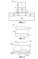
- FIG. 1shows an embodiment of an atomic layer deposition system 100 for processing a dielectric film containing a Ta x Ln y O z N r layer.
- the elements depictedare those elements necessary for discussion of various embodiments for forming TaLnON such that those skilled in the art may practice embodiments of the present invention without undue experimentation.
- a substrate 110is located inside a reaction chamber 120 of ALD system 100 .
- a heating element 130which is thermally coupled to substrate 110 to control the substrate temperature.
- a gas-distribution fixture 140introduces precursor gases to the substrate 110 . Each precursor gas originates from individual gas sources 150 - 155 whose flow is controlled by mass-flow controllers 156 - 161 , respectively.
- Gas sources 150 - 155provide a precursor gas either by storing the precursor as a gas or by providing a location and apparatus for evaporating a solid or liquid material to form the selected precursor gas. Furthermore, additional gas sources may be included, one for each metal precursor employed and one for each reactant precursor associated with each metal precursor.
- purging gas sources 163 , 164are also included in the ALD system.
- additional purging gas sourcesmay be constructed in ALD system 100 , one purging gas source for each precursor gas. For a process that uses the same purging gas for multiple precursor gases, less purging gas sources are required for ALD system 100 .
- Gas sources 150 - 155 and purging gas sources 163 - 164are coupled by their associated mass-flow controllers to a common gas line or conduit 170 , which is coupled to the gas-distribution fixture 140 inside reaction chamber 120 .
- Gas conduit 170is also coupled to vacuum pump, or exhaust pump, 181 by mass-flow controller 186 to remove excess precursor gases, purging gases, and by-product gases at the end of a purging sequence from gas conduit 170 .
- Vacuum pump, or exhaust pump, 182is coupled by mass-flow controller 187 to remove excess precursor gases, purging gases, and by-product gases at the end of a purging sequence from reaction chamber 120 .
- mass-flow controller 187to remove excess precursor gases, purging gases, and by-product gases at the end of a purging sequence from reaction chamber 120 .
- control displays, mounting apparatus, temperature sensing devices, substrate maneuvering apparatus, and necessary electrical connections as are known to those skilled in the artare not shown in FIG. 1 .
- the use, construction and fundamental operation of reaction chambers for deposition of filmsare understood by those of ordinary skill in the art of semiconductor fabrication. Embodiments of the present invention may be practiced on a variety of such reaction chambers without undue experimentation.
- one of ordinary skill in the artwill comprehend the necessary detection, measurement, and control techniques in the art of semiconductor fabrication upon reading the disclosure.
- a tantalum lanthanide oxynitride layermay be structured as one or more monolayers.
- a film of tantalum lanthanide oxynitride, structured as one or more monolayers,may have a thickness that ranges from a monolayer to thousands of angstroms or more.
- the filmmay be processed using atomic layer deposition.
- Embodiments of an atomic layer deposited tantalum lanthanide oxynitride layerhave a larger dielectric constant than silicon dioxide.
- Such dielectric layersprovide a significantly thinner equivalent oxide thickness compared with a silicon oxide layer having the same physical thickness.
- such dielectric layersprovide a significantly thicker physical thickness than a silicon oxide layer having the same equivalent oxide thickness. This increased physical thickness aids in reducing leakage current.
- the surface on which the tantalum lanthanide oxynitride film is to be depositedmay undergo a preparation stage.
- the surfacemay be the surface of a substrate for an integrated circuit.
- the substrate used for forming a transistormay include a silicon or silicon containing material.
- silicon germanium, germanium, gallium arsenide, silicon-on-sapphire substrates, or other suitable substratesmay be used.
- a preparation processmay include cleaning the substrate and forming layers and regions of the substrate, such as drains and sources, prior to forming a gate dielectric in the formation of a metal insulator semiconductor (MIS) transistor.
- MISmetal insulator semiconductor
- active regionsmay be formed after forming the dielectric layer, depending on the over-all fabrication process implemented.
- the substrateis cleaned to provide an initial substrate depleted of its native oxide.
- the initial substrateis cleaned also to provide a hydrogen-terminated surface.
- a silicon substrateundergoes a final hydrofluoric (HF) rinse prior to ALD processing to provide the silicon substrate with a hydrogen-terminated surface without a native silicon oxide layer.
- HFfinal hydrofluoric
- Cleaning immediately preceding atomic layer depositionaids in reducing an occurrence of silicon oxide as an interface between a silicon-based substrate and a tantalum lanthanide oxynitride dielectric formed using the atomic layer deposition process.
- the material composition of an interface layer and its propertiesare typically dependent on process conditions and the condition of the substrate before forming the dielectric layer. Though the existence of an interface layer may effectively reduce the dielectric constant associated with the dielectric layer and its substrate interface layer, a SiO 2 interface layer or other composition interface layer may improve the interface density, fixed charge density, and channel mobility of a device having this interface layer.
- the sequencing of the formation of the regions of an electronic device, such as a transistor, being processedmay follow typical sequencing that is generally performed in the fabrication of such devices as is well known to those skilled in the art. Included in the processing prior to forming a dielectric may be the masking of substrate regions to be protected during the dielectric formation, as is typically performed in semiconductor fabrication. In an embodiment, an unmasked region includes a body region of a transistor; however, one skilled in the art will recognize that other semiconductor device structures may utilize this process.
- a purging gasmay be pulsed into the ALD reaction chamber.
- the ALD reactor chambermay be evacuated using vacuum techniques as is known by those skilled in the art.
- a purging gasmay be pulsed into the ALD reaction chamber and the ALD reactor chamber may be evacuated.
- an ALD cycle for forming TaLnONincludes sequencing component-containing precursors in the order of lanthanide, oxygen, tantalum, and nitrogen with appropriate purging between the different component-containing precursors. Full coverage or partial coverage of a monolayer on a substrate surface may be attained for pulsing of a metal-containing precursor.
- an ALD cycle for forming TaLnONincludes sequencing the component-containing precursors in various permutations.
- an ALD cycle to form tantalum lanthanide oxynitrideincludes a number, x, of lanthanide/oxygen sequences and a number, y, of tantalum/nitrogen sequences.
- an ALD cycle to form tantalum lanthanide oxynitrideincludes a number, x, of lanthanide/nitrogen sequences and a number, y, of tantalum/oxygen sequences.
- the number of sequences x and yis selected to engineer the relative amounts of tantalum, lanthanide, oxygen, and nitrogen.
- the number of sequences x and yis selected to form a nitrogen-rich tantalum lanthanide oxynitride.
- the number of sequences x and yare selected to form an oxygen-rich tantalum lanthanide oxynitride.
- the tantalum lanthanide oxynitridemay be engineered as a lanthanide-rich dielectric relative to the amount of tantalum in the dielectric.
- the tantalum lanthanide oxynitridemay be engineered as a tantalum-rich dielectric relative to the amount of lanthanide in the dielectric.
- the pulsing of the individual component-containing precursorsmay be performed independently in a non-overlapping manner using the individual gas sources 150 - 155 and flow controllers 156 - 161 of ALD system 100 of FIG. 1 .
- Each precursormay be pulsed into the reaction chamber for a predetermined period, where the predetermined period can be set separately for each precursor. Additionally, for various ALD formations, each precursor may be pulsed into the reaction chamber under separate environmental conditions.
- the substratemay be maintained at a selected temperature and the reaction chamber maintained at a selected pressure independently for pulsing each precursor. Appropriate temperatures and pressures may be maintained, whether the precursor is a single precursor or a mixture of precursors.
- a number of precursors containing a lanthanidemay be used to provide the lanthanide to a substrate for an integrated circuit.
- a lanthanum-containing precursoris pulsed onto a substrate in an ALD reaction chamber.
- Meis an abbreviation for CH 3
- Etis an abbreviation for ethyl (CH 2 CH 3 )
- Cpis an abbreviation for a cyclopentadienyl ligand having the formula C 5 H 5 .
- H 2may be pulsed along with a La(EtCp) 3 precursor or a La(DPM) 3 precursor to reduce carbon contamination in the fabricated film.
- Other precursorsmay be used in embodiments in which the lanthanide is other than lanthanum.
- a reactant precursormay be pulsed into the reaction chamber.
- the reactant precursormay be an oxygen reactant precursor, for a lanthanum/oxygen sequence, that may include, but is not limited to, one or more of water, atomic oxygen, molecular oxygen, ozone, hydrogen peroxide, a water—hydrogen peroxide mixture, alcohol, or nitrous oxide.
- the reactant precursormay be a nitrogen reactant precursor, for a lanthanum/nitrogen sequence, that may include, but is not limited to, nitrogen, ammonia (NH 3 ), tert-butylamine (C 4 H 11 N), allylamine (C 3 H 7 N), 1,1-dimethylhydrazine ((CH 3 ) 2 NNH 2 ).
- the pulsing of the lanthanide precursormay use a pulsing period that provides uniform coverage of a monolayer on the surface or may use a pulsing period that provides partial coverage of a monolayer on the surface during a lanthanide sequence.
- a number of precursors containing tantalummay be used to provide the tantalum to a substrate for an integrated circuit.
- Precursors containing tantalummay include, but are not limited to, tantalum ethoxide [Ta(OC 2 H 5 ) 5 ] and tantalum halides, such as TaCl 5 , TaBr 5 , and TaF 5 .
- a reactant precursormay be pulsed into the reaction chamber.
- the reactant precursormay be an nitrogen reactant precursor, for a tantalum/nitrogen sequence, that may include, but is not limited to, one or more of nitrogen, ammonia (NH 3 ), tert-butylamine (C 4 H 11 N), allylamine (C 3 H 7 N), 1,1-dimethylhydrazine ((CH 3 ) 2 NNH 2 ).
- the reactant precursormay be an oxygen reactant precursor, for a tantalum/oxygen sequence, that may include, but is not limited to, one or more of water, atomic oxygen, molecular oxygen, ozone, hydrogen peroxide, a water—hydrogen peroxide mixture, alcohol, or nitrous oxide.
- the pulsing of the tantalum precursormay use a pulsing period that provides uniform coverage of a monolayer on the surface or may use a pulsing period that provides partial coverage of a monolayer on the surface during a tantalum sequence.
- nitrogenmay be used as a purging gas and a carrier gas for one or more of the sequences used in the ALD formation of tantalum lanthanide oxynitride.
- hydrogen, argon gas, or other inert gasesmay be used as the purging gas.
- Excess precursor gas and reaction by-productsmay be removed by the purge gas.
- Excess precursor gas and reaction by-productsmay be removed by evacuation of the reaction chamber using various vacuum techniques.
- Excess precursor gas and reaction by-productsmay be removed by the purge gas and by evacuation of the reaction chamber.
- the thickness of a tantalum lanthanide oxynitride layer formed by atomic layer depositionis determined by a fixed growth rate for the pulsing periods and precursors used, set at a value such as N nm/cycle, and the number of cycles conducted.
- the processis conducted in an ALD window, which is a range of temperatures in which the growth rate is substantially constant. In an embodiment, if such an ALD window is not available, the ALD process is conducted at the same set of temperatures for each ALD sequence in the process. For a desired tantalum lanthanide oxynitride layer thickness, t, in an application, the ALD process is repeated for t/N total cycles. Once the t/N cycles have completed, no further ALD processing for the tantalum lanthanide oxynitride layer is required. In an embodiment, a tantalum lanthanide oxynitride layer processed at relatively low temperatures associated with atomic layer deposition provides an amorphous layer.
- a TaLnON filmmay be grown to a desired thickness by repetition of a process including atomic layer deposition of layers of LnO and TaN and/or layers of TaO and LnN followed by annealing.
- a base thicknessmay be formed according to various embodiments such that forming a predetermined thickness of a TaLnON film may be conducted by forming a number of layers having the base thickness. As can be understood by one skilled in the art, determining the base thickness depends on the application and can be determined during initial processing without undue experimentation.
- Relative amounts of tantalum, lanthanide, oxygen, and nitrogen in a TaLnON filmmay be controlled by regulating the relative thicknesses of the individual layers of oxides and nitrides formed.
- relative amounts of tantalum, lanthanide, oxygen, and nitrogen in a TaLnON filmmay be controlled by forming a layer of TaLnON as multiple layers of different base thickness and by regulating the relative thicknesses of the individual layers of oxides and nitrides formed in each base layer prior to annealing.
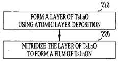
- FIG. 2Ashows a flow diagram of features of an embodiment for forming TaLnON using atomic layer deposition and nitridization.
- a layer of TaLnOis formed using atomic layer deposition.
- the layer of TaLnOis subjected to a nitridization to form a TaLnON film.
- the nitridizationmay be a high temperature nitridization.
- active nitrogenmay be introduced by microwave plasma.
- active nitrogenmay be introduced by a NH 3 anneal.
- a high temperature nitridizationis a nitridizing process that is performed at temperatures equal to or above 500° C.
- TaLnOmay be formed by atomic layer deposition using ALD cycles of lanthanide/oxygen sequences and tantalum/oxygen sequences.
- the ALD cyclecan be selected from a number of different permutations of lanthanide/oxygen sequences and tantalum/oxygen sequences.
- FIG. 2Bshows a flow diagram of features of an embodiment for forming TaLnO using atomic layer deposition for nitridization to a TaLnON film.
- a layer of lanthanide oxideis formed on a substrate by atomic layer deposition.
- a layer of tantalum oxideis formed by atomic layer deposition on the layer of lanthanide oxide.
- the layers of lanthanide oxide and tantalum oxideare annealed to form a layer of TaLnO.
- the order of forming LnO and TaOmay be interchanged.
- the layer of TaLnOmay be nitridized to form TaLnON.
- the layers of lanthanide oxide and tantalum oxidemay be nitridized during the annealing process.
- alternating layers of ALD lanthanide oxide and ALD tantalum oxidemay be formed to a desired thickness prior to nitridization.
- a layer of ALD lanthanide oxide and a layer of ALD tantalum oxidemay be formed, each to a desired thickness, the layers of ALD lanthanide oxide and ALD tantalum oxide nitridized to form a TaLnON layer.
- a layer of ALD lanthanide oxide and a layer of ALD tantalum oxidemay be formed on the TaLnON layer, the layers of ALD lanthanide oxide and ALD tantalum oxide nitridized to form a TaLnON layer on and contiguous with the previously formed TaLnON layer. This process may be continued until the desired thickness of TaLnON is formed.
- ALD LaOmay be formed using a number of precursors containing lanthanum to provide the lanthanum to a substrate for an integrated circuit.
- lanthanum-containing precursorsinclude, but are not limited to, La(thd) 3 , tris (2,2,6,6-tetramethyl-3,5-heptanedionato)lanthanum (III) tetraglyme adduct, La(EtCp) 3 , and La(DPM) 3 .
- the oxygen reactant precursormay include, but is not limited to, one or more of water, atomic oxygen, molecular oxygen, ozone, hydrogen peroxide, a water—hydrogen peroxide mixture, alcohol, or nitrous oxide.
- the reaction chambermay be purged of excess precursor and by-products.
- the pulsing of the precursorsmay use pulsing periods that provide uniform coverage of a monolayer on the surface or may use pulsing periods that provide partial coverage of a monolayer on the surface during a lanthanum/oxygen ALD cycle.
- ALD TaOmay be formed using a number of precursors containing tantalum to provide the tantalum to a substrate for an integrated circuit.
- tantalum-containing precursorsinclude, but are not limited to, Ta(OC 2 H 5 ) 5 and a tantalum halide, such as TaCl 4 and TaI 4 .
- an oxygen reactant precursormay be pulsed into the reaction chamber.
- the oxygen reactant precursormay include, but is not limited to, one or more of water, atomic oxygen, molecular oxygen, ozone, hydrogen peroxide, a water—hydrogen peroxide mixture, alcohol, or nitrous oxide.
- the pulsing of the precursorsmay use pulsing periods that provide uniform coverage of a monolayer on the surface or may use pulsing periods that provide partial coverage of a monolayer on the surface during an ALD cycle forming TaO.
- nitrogenmay be used as a purging gas and a carrier gas for one or more of the sequences.
- hydrogen, argon gas, or other inert gasesmay be used as the purging gas.
- Excess precursor gas and reaction by-productsmay be removed by the purge gas.
- Excess precursor gas and reaction by-productsmay be removed by evacuation of the reaction chamber using various vacuum techniques.
- Excess precursor gas and reaction by-productsmay be removed by the purge gas and by evacuation of the reaction chamber.
- FIG. 3shows a flow diagram of features of an embodiment for forming TaLnON using atomic layer deposition and oxidation.
- a layer of TaNis formed by atomic layer deposition.
- a layer of LnNis formed by atomic layer deposition on the layer of TaN.
- TaN and LnN filmsmay be alternately deposited in adjacent layers, in which either nitride layer may be deposited as the starting layer.
- the layers of LnN and TaNare annealed.
- the annealed layers of LnN and TaNare oxidized to form TaLnON. In an embodiment, the annealing and oxidation may be performed together.
- the layers of LnN and TaNmay be annealed and oxidized by rapid thermal oxidation to form TaLnON.
- ALD TaNmay be formed using a number of precursors containing tantalum to provide the tantalum to a substrate for an integrated circuit.
- a tantalum-containing precursoris pulsed onto a substrate in an ALD reaction chamber.
- a number of precursors containing tantalummay be used to provide the tantalum to a substrate for an integrated circuit.
- a number of precursors containing tantalummay be used to provide the tantalum to a substrate for an integrated circuit.
- Precursors containing tantalummay include, but are not limited to, tantalum ethoxide [Ta(OC 2 H 5 ) 5 ] and tantalum halides, uch as TaCl 5 , TaBr 5 , and TaF 5 .
- a nitrogen reactant precursormay be pulsed into the reaction chamber.
- the reactant precursor for a tantalum/nitrogen sequencemay include, but is not limited to, nitrogen, ammonia (NH 3 ), tert-butylamine (C 4 H 11 N), allylamine (C 3 H 7 N), 1,1-dimethylhydrazine ((CH 3 ) 2 NNH 2 ).
- Other nitrogen reactant precursors that may be usedinclude nitrogen-containing compositions that do not include oxygen.
- nitrogen reactant precursorsare not limited to nitrogen-containing compositions that do not include oxygen.
- forming tantalum nitride by atomic layer depositionis not limited to the abovementioned precursors.
- the pulsing of the tantalum precursormay use a pulsing period that provides uniform coverage of a monolayer on the surface or may use a pulsing period that provides partial coverage of a monolayer on the surface during a tantalum sequence.
- ALD LaNmay be formed using a number of precursors containing lanthanum to provide the lanthanum to a substrate for an integrated circuit.
- lanthanum-containing precursorsinclude, but are not limited to, La(thd) 3 , tris (2,2,6,6-tetramethyl-3,5-heptanedionato)lanthanum (III) tetraglyme adduct, La(EtCp) 3 , and La(DPM) 3 .
- the substratemay be maintained at a temperature ranging from 180° C. to about 425° C.
- H 2may be pulsed along with the La(EtCp) 3 precursor or the precursor to reduce carbon contamination in the deposited film.
- a reactant precursormay be pulsed into the reaction chamber.
- a nitrogen reactant precursoris pulsed.
- a number of precursors containing nitrogenmay be used to provide nitrogen.
- nitrogen-containing precursorsinclude, but are not limited to, nitrogen, ammonia (NH 3 ), tert-butylamine (C 4 H 11 N), allylamine (C 3 H 7 N), 1,1-dimethylhydrazine ((CH 3 ) 2 NNH 2 ).
- the substrateis maintained at a temperature ranging from about 400° C. to about 500° C. using tert-butylamine or allylamine as a nitrogen precursor.
- NH 3may be pulsed with the tert-butylamine and the allylamine. The addition of NH 3 may enhance the deposition rate at lower temperatures.
- use of the individual lanthanum-containing precursorsis not limited to the temperature ranges of the above example embodiments. Further, forming lanthanum nitride by atomic layer deposition is not limited to the abovementioned precursors.
- the pulsing of the lanthanum precursormay use a pulsing period that provides uniform coverage of a monolayer on the surface or may use a pulsing period that provides partial coverage of a monolayer on the surface during a lanthanum/nitrogen sequence.
- nitrogenmay be used as a purging gas and a carrier gas for one or more of the sequences.
- hydrogen, argon gas, or other inert gasesmay be used as the purging gas.
- Excess precursor gas and reaction by-productsmay be removed by the purge gas.
- Excess precursor gas and reaction by-productsmay be removed by evacuation of the reaction chamber using various vacuum techniques.
- Excess precursor gas and reaction by-productsmay be removed by the purge gas and by evacuation of the reaction chamber.
- FIG. 4shows a flow diagram of features of an embodiment for forming TaLnON using atomic layer deposition and annealing.
- a layer of TaONis formed using atomic layer deposition.
- a layer of LnONis formed using atomic layer deposition on the layer of TaON.
- the layers of TaON and LnONare annealed to form a layer of TaLnON.
- TaON and LnON filmsmay be alternately deposited in adjacent layers, in which either oxynitride layer may be deposited as the starting layer.
- ALD LaONmay be formed using a number of precursors containing lanthanum to provide the lanthanum to a substrate for an integrated circuit.
- lanthanum-containing precursorsinclude, but are not limited to, La(thd) 3 , tris (2,2,6,6-tetramethyl-3,5-heptanedionato)lanthanum (III) tetraglyme adduct, La(EtCp) 3 , and La(DPM) 3 .
- a number of precursors containing nitrogenmay be used to provide nitrogen.
- nitrogen-containing precursorsinclude, but are not limited to, nitrogen, ammonia (NH 3 ), tert-butylamine (C 4 H 11 N), allylamine (C 3 H 7 N), 1,1-dimethylhydrazine ((CH 3 ) 2 NNH 2 ).
- an oxygen reactant precursormay be pulsed into the reaction chamber.
- the oxygen reactant precursormay include, but is not limited to, one or more of water, atomic oxygen, molecular oxygen, ozone, hydrogen peroxide, a water—hydrogen peroxide mixture, alcohol, or nitrous oxide.
- the order of pulsing the precursorsmay vary. In various embodiments, forming lanthanum oxynitride by atomic layer deposition is not limited to the abovementioned precursors.
- the pulsing of the precursorsmay use pulsing periods that provide uniform coverage of a monolayer on the surface or may use pulsing periods that provide partial coverage of a monolayer on the surface during an ALD cycle forming LaON.
- ALD TaONmay be formed using a number of precursors containing tantalum to provide the tantalum to a substrate for an integrated circuit.
- tantalum-containing precursorsinclude, but are not limited to, Ta(OC 2 H 5 ) 5 and one or more tantalum halides.
- a nitrogen reactant precursormay be pulsed into the reaction chamber.
- the reactant precursormay include, but is not limited to, nitrogen, NH 3 , C 4 H 11 N, C 3 H 7 N, and (CH 3 ) 2 NNH 2 .
- nitrogen reactant precursorsthat may be used include nitrogen-containing compositions that do not include oxygen.
- the nitrogen-containing precursormay also include oxygen.
- an oxygen reactant precursormay be pulsed into the reaction chamber.
- the oxygen reactant precursormay include, but is not limited to, one or more of water, atomic oxygen, molecular oxygen, ozone, hydrogen peroxide, a water—hydrogen peroxide mixture, alcohol, or nitrous oxide.
- the order of pulsing the precursorsmay vary. Further, forming tantalum oxynitride by atomic layer deposition is not limited to the abovementioned precursors.
- the pulsing of the precursorsmay use pulsing periods that provide unifonm coverage of a monolayer on the surface or may use pulsing periods that provide partial coverage of a monolayer on the surface during an ALD cycle forming TaON.
- nitrogenmay be used as a purging gas and a carrier gas for one or more of the sequences.
- hydrogen, argon gas, or other inert gasesmay be used as the purging gas.
- Excess precursor gas and reaction by-productsmay be removed by the purge gas.
- Excess precursor gas and reaction by-productsmay be removed by evacuation of the reaction chamber using various vacuum techniques.
- Excess precursor gas and reaction by-productsmay be removed by the purge gas and by evacuation of the reaction chamber.
- a dielectric stack containing a TaLnON x filmincludes a silicon oxide layer.
- the dielectric layeris formed as a nanolaminate.
- An embodiment of a nanolaminateincludes a layer of a tantalum oxide and a TaLnON x film, a layer of tantalum oxynitride and a TaLnON x film, a layer of lanthanide oxide and a TaLnON x film, a layer of lanthanide oxynitride and a TaLnON x film, layers of tantalum oxide, lanthanide oxide, tantalum oxynitride, and lanthanide oxynitride along with a TaLnON x film, or various other combinations.
- a dielectric layeris formed substantially as the tantalum lanthanide oxynitride film.
- the structure of an interface between a dielectric layer and a substrate on which it is disposedis controlled to limit the inclusion of silicon oxide, since a silicon oxide layer would reduce the effective dielectric constant of the dielectric layer.
- the material composition and properties for an interface layerare dependent on process conditions and the condition of the substrate before forming the dielectric layer.
- the interface layersuch as a silicon oxide interface layer or other composition interface layer, may improve the interface density, fixed charge density, and channel mobility of a device having this interface layer.
- a tantalum lanthanide oxynitride layeris doped with other elements.
- the dopingmay be employed to enhance the leakage current characteristics of the dielectric layer containing the TaLnON x film by providing a disruption or perturbation of the tantalum lanthanide oxynitride structure.
- such dopingis realized by substituting a sequence of one of these elements for a tantalum sequence, a lanthanide sequence, or various combinations of sequences. The choice for substitution may depend on the form of the tantalum lanthanide oxynitride structure with respect to the relative amounts of tantalum atoms and lanthanide atoms desired in the oxide.
- the amount of dopants inserted into the oxynitrideare limited to a relatively small fraction of the total number of tantalum and lanthanide atoms.
- the other materialmay be formed upon the tantalum lanthanide oxynitride layer.
- the other materialis a conductive material.
- the conductive materialmay be used as an electrode. Such electrodes may be used as capacitor electrodes, control gates in transistors, or floating gates in floating gate transistors.
- the conductive materialis a metal or conductive metal nitride.
- the conductive materialis a conductive semiconductor material.
- the conductive materialis formed by ALD processes.
- the conductive materialis formed by a substitution process.
- the conductive materialis formed in a self-alignment process.
- a conductive layermay be deposited by atomic layer deposition on a layer of TaLnON or on a dielectric layer containing a layer of TaLnON.
- a metal layermay be deposited by atomic layer deposition in an ALD cycle having a halide precursor containing the metal to be deposited and a reactant precursor containing hydrogen.
- Metal layer formation by ALDis not limited to halide precursors and hydrogen reactant precursors.
- precursorsmay be selected to form ALD conductive layers such as aluminum (Al), tungsten (W), molybdenum (Mo), gold (Au), silver (Ag), gold alloy, silver alloy, copper (Cu), platinum (Pt), rhenium (Re), ruthenium (Ru), rhodium (Rh), nickel (Ni), osmium (Os), palladium (Pd), iridium (Ir), cobalt (Co), germanium (Ge), or metallic nitrides such as WN, TiN or TaN. Formation of ALD conductive layers is not limited to the abovementioned materials.
- a tantalum layermay be formed on a TaLnON film by atomic layer deposition using a tantalum-containing precursor.
- a tantalum halide precursormay be used with hydrogen as a reactant precursor.
- a TaCl 5 precursormay be used with an atomic hydrogen reactant precursor.
- the atomic hydrogen reactant precursormay be provided using a plasma.
- the substrate temperaturemay be held at a temperature ranging from about 250° C. to about 400° C. The hydrogen reactant precursor reacts at the substrate to remove the halogen, which forms the selected tantalum halide precursor, leaving tantalum on the substrate surface.
- the reaction chambermay be purged of excess precursor and/or by-products.
- use of the individual tantalum-containing precursorsis not limited to the temperature ranges of the above example embodiments.
- forming tantalum by atomic layer depositionis not limited to the abovementioned precursors.
- the pulsing of the tantalum precursormay use a pulsing period that provides uniform coverage of a monolayer on the surface or may use a pulsing period that provides partial coverage of a monolayer on the surface.
- the tantalum layermay be structured as one or more monolayers.
- the tantalum layermay have a thickness ranging from a monolayer to thousands of angstroms or more.
- a metal nitride layermay be deposited by atomic layer deposition using a precursor containing the metal to be deposited and a reactant precursor containing nitrogen in an ALD cycle.
- a titanium nitride layermay be formed with a TaLnON film by atomic layer deposition using a titanium-containing precursor.
- a nitrogen-containing precursormay be used as the reactant precursor for the titanium-containing precursor.
- the titanium-containing precursor and the nitrogen-containing precursormay be selected such that their use does not form a titanium oxide in the layer of titanium nitride being formed.
- the titanium-containing precursor and the nitrogen-containing precursormay be selected such that these precursors do not include oxygen as an elemental component.
- a titanium halide precursormay be used with NH 3 as a reactant precursor.
- a TiCl 4 precursormay be used with a NH 3 reactant precursor.
- the substrate temperaturemay be held at a temperature ranging from about 380° C. to about 500° C. In an embodiment, the substrate temperature may be held at a temperature less than 600° C. After pulsing a titanium-containing precursor and after pulsing its reactant precursor, the reaction chamber may be purged of excess precursor and/or by-products. In various embodiments, use of the individual titanium-containing precursors is not limited to the temperature ranges of the above example embodiments.
- titanium nitride by atomic layer depositionis not limited to the abovementioned precursors, but may include precursors containing oxygen.
- the pulsing of the titanium precursormay use a pulsing period that provides uniform coverage of a monolayer on the surface or may use a pulsing period that provides partial coverage of a monolayer on the surface.
- the titanium nitride layermay be structured as one or more monolayers.
- the titanium nitride layermay have a thickness ranging from a monolayer to thousands of angstroms or more.
- FIGS. 5A-5Eillustrate an embodiment of a process for forming a metal substituted electrode in place of a previously deposited material on a dielectric containing TaLnON. Though a transistor is discussed with reference to FIGS. 5A-5E , such a process may be used with respect to other embodiments of device configurations.
- FIG. 5Ashows a substrate 501 and shallow trench isolation (STI) regions 502 .
- the substrate 501can be a semiconductor wafer as well as structures having one or more insulative, semi-insulative, conductive, or semiconductive layers and materials.
- the substratecan include silicon-on-insulator, silicon-on-sapphire, and other structures upon which semiconductor devices are formed.
- FIG. 5Bfurther shows a gate dielectric layer 503 formed on the substrate 501 , and a gate substitutable layer 504 formed on the gate dielectric layer 503 .
- the gate dielectric layermay include a dielectric layer containing TaLnON in addition to other insulative material or a dielectric layer essentially of TaLnON. The use of such a high- ⁇ dielectric increases the capacitance, which is useful for nanoscale integrated circuits.
- the gate dielectricincludes stacked layers comprising one or more high- ⁇ dielectric materials.
- the material of the gate substitutable layer 504is selected with respect to the desired gate material to allow the gate material to replace the gate substitutable layer. This process forms a gate of the desired gate metal where the substitutable material was positioned on the gate dielectric.
- Source/drain regions 507are also formed. Source/drain regions 507 can be formed using conventional ion implantation and subsequent annealing. These annealing temperatures can pose problems for aluminum gates and other metal gates that have melting temperatures less than the anneal temperature for the source/drain regions.
- FIG. 5Dshows an insulative fill layer 508 provided to match the thickness of the gate stack.
- a planarization proceduresuch as chemical-mechanical polishing, can be used to provide an even surface across the fill layer 508 and the gate substitutable layer 504 .
- a metal layer 509formed of material intended to be the gate material, is deposited over the gate substitutable layer 504 and the fill layer 508 .
- the metal layer 509is also referred to herein as a layer of gate material.
- Various deposition processessuch as evaporation, sputtering, chemical vapor deposition, or atomic layer deposition, may be used to form the metal layer 509 .
- the volume of layer 509is significantly larger than the volume of the substitutable material left on the wafer.
- a metal-substitution reactionis induced.
- the reactioncan be provided by annealing the structure in a non-oxidizing atmosphere such as a nitrogen gas or a forming gas. The heating urges diffusion or dissolution of the intended gate material in metal layer 509 for the substitutable material 504 .
- the substitution processis bounded by the spacers 506 and the gate dielectric 503 .
- FIG. 5Eshows the resulting low-resistance gate structure.
- the illustrated structureincludes a metal substituted gate 510 formed by the substitution of the metal of layer 509 .
- the metal substituted gate 510may include a small amount of the gate substitutable material that did not diffuse above the planarization level 511 . Such small amounts of the gate substitutable material do not significantly affect the conductivity of the metal substituted gate 510 , and thus do not significantly affect the performance of the device.
- Drain and source contactscan be formed, as well as interconnects to other transistors or components, using conventional techniques. Another heat treatment may occur after packaging the integrated circuit in a protective housing in an attempt to reduce the resistivity of the metal gate contacts and other metal interconnections.
- the metal gate substitution techniquecan be applied to MOS devices, as generally illustrated in FIG. 5E , as well as to form metal floating gates and/or metal control gates in nonvolatile devices. Additionally, various high- ⁇ dielectrics having a TaLnON film can be used between the floating gate and the substrate, and between the control gate and the floating gate in these nonvolatile devices.
- FIG. 6illustrates a flow diagram of features of an embodiment of a metal substitution technique.
- a gate dielectricis formed on a substrate.
- the gate dielectricincludes a TaLnON film.
- a layer of gate substitutable materialis formed on the gate dielectric. Examples of gate substitutable material include polysilicon, germanium, silicon-germanium, and carbon.
- source/drain regionsare formed.
- a layer of gate materialis formed at 615 on the gate substitutable material. Examples of such metals include gold, silver, and aluminum. Other metals may be used.
- the gate materialis substituted for the layer of gate substitutable material.
- a metal substitution reactionsubstitutes or replaces the substitutable material (e.g. silicon, germanium, silicon-germanium, carbon) with a metal. After the substitution, the resulting gate structure includes substantially all of the desired metal. Small amounts of the substitutable material may remain in the gate structure.
- the substitution reactioncan be induced by heating the integrated circuit assembly to a desired temperature in a vacuum, nitrogen, argon, forming gas or other non-oxidizing atmosphere. Heating causes diffusion of the metal layer 609 into the substitutable layer.
- the annealing temperature for the substitutionis less than the eutectic (lowest melting) temperature of materials involved in the substitution for the reaction for substitution to occur.
- a metal layermay be formed from gold and annealed at approximately 300° C.
- a metal layermay be formed from silver and annealed at approximately 500-600° C. to substitute the silver for a silicon substitutable structure.
- a polysilicon and germanium substitutable materialmay be used, which reduces the anneal temperature.
- the gate substitutable material 504 shown in FIGS. 5A-5Eincludes polysilicon.
- the gate substitutable materialincludes germanium.
- Some embodimentsuse silicon-germanium with a percentage of silicon in the range from 0% to 100% as the gate substitutable material 504 .
- Some embodimentsuse carbon as the gate substitutable material 504 .
- a replacement metal for the substituted gatemay include aluminium, silver, gold, an alloy of silver, an alloy of gold as the replacement metal, or combinations thereof.
- a replacement metal for the substituted gatemay include gold, silver, an alloy of gold, an alloy of silver, copper, platinum, rhenium, ruthenium, rhodium, nickel, osmium, palladium, iridium, cobalt, germanium, or combinations thereof.
- Various embodimentsform an integrated circuit structure using two or more substitution reactions. Relatively higher temperature substitution processes can be performed before relatively lower temperature substitution processes.
- One application for multiple substitution reactionsis to independently adjust work functions of NMOS and PMOS transistors in CMOS integrated circuits. Multiple substitution reactions are not limited to this CMOS integrated circuit application. Additional information regarding metal substitution can be found in U.S. patent application Ser. No. 11/176,738 filed Jul. 7, 2005, entitled “METAL-SUBSTITUTED TRANSISTOR GATES,” which is herein incorporated by reference.
- FIGS. 7A-7Dillustrate an embodiment of a process for forming a self aligned conductive layer such as a metal gate for a transistor structure.
- FIG. 7Aillustrates a high- ⁇ gate dielectric 710 containing TaLnON formed on a substrate 701 .
- the substrate 701can be a semiconductor wafer as well as structures having one or more insulative, semi-insulative, conductive, or semiconductive layers and materials.
- the substratecan include silicon-on-insulator, silicon-on-sapphire, and other structures upon which semiconductor devices are formed.
- a sacrificial gate 703is formed of amorphous carbon on the high- ⁇ gate dielectric 710 .
- an etch barrier 708is formed over the sacrificial gate and the dielectric.
- the etch barrier 708includes silicon nitride or aluminium oxide, and can be formed using a deposition process, according to various embodiments.
- Sacrificial sidewall spacers 706are added adjacent the sacrificial gate 703 .
- the spacers 706are formed of amorphous carbon by deposition and conventional direct etch techniques.
- An ion implantation 730 and high temperature annealare used to form source/drain regions 702 in areas defined by the sacrificial sidewall spacers 706 . These annealing temperatures can pose problems for aluminum gates and other metal gates that have melting temperatures less than the anneal temperature for the source/drain regions.
- FIG. 7Bthe sacrificial sidewall spacers ( 706 in FIG. 7A ) have been removed.
- Various embodimentsuse a plasma oxidation process to remove the sacrificial sidewall spacers.
- the etch barrier ( 708 in FIG. 7A )has been removed.
- a light dose ion implantation 740is used to form source/drain extensions 742 in the substrate 701 .
- the extensions 742can be annealed at lower temperatures and in shorter times than the more heavily doped source/drain regions 702 .
- source/drain extensions for the transistormay be formed with doping the substrate to a depth of 30 nm or less.
- conventional or non-carbon sidewall spacers 756are formed and the whole structure is back filled with an oxide fill 758 , such as silicon dioxide, and planarized.
- oxide fill 758such as silicon dioxide
- the conventional sidewall spacersare formed with silicon nitride.
- the sacrificial gate( 703 in FIG. 7C ) is removed and replaced by the deposition of a metal layer 760 .
- the sacrificial gateis removed using a plasma oxidation process.
- Various deposition processessuch as evaporation, sputtering, chemical vapor deposition, or atomic layer deposition, may be used to form the metal layer 760 .
- the structureis planarized (not shown) using a planarization procedure, such as chemical-mechanical polishing, resulting in the self aligned metal gate over the high-K gate dielectric insulator 710 .
- Drain and source contacts(not shown) can be formed, as well as interconnects to other transistors or components, using conventional techniques. Another heat treatment may occur after packaging the integrated circuit in a protective housing in an attempt to reduce the resistivity of the metal gate contacts and other metal interconnections.
- FIGS. 7A-7Dillustrate two replacement processes for the formation of planar self aligned metal gate transistors, one for disposable sidewall spacers and the other for the gate material itself.
- the metal gate replacement techniqueas disclosed herein, can be applied to MOS devices, as generally illustrated in FIGS. 7A-7D , as well as to form metal floating gates and/or metal control gates in nonvolatile devices. Additionally, various high- ⁇ dielectrics can be used between the floating gate and the substrate, and between the control gate and the floating gate in these nonvolatile devices.
- FIG. 8illustrates an embodiment of a method 800 for forming a self aligned metal gate on high-K gate dielectrics containing TaLnON.
- a high-K gate dielectric containing TaLnONis formed on a substrate, at 802 .
- a sacrificial carbon gateis formed on the gate dielectric.
- sacrificial carbon sidewall spacersare formed adjacent to the sacrificial carbon gate.
- source/drain regions for the transistorare formed, using the sacrificial carbon sidewall spacers to define the source/drain regions.
- the sacrificial carbon sidewall spacersare replaced with non-carbon sidewall spacers at 810 .
- the sacrificial carbon gateis replaced with a desired metal gate material to provide the desired metal gate material on the gate dielectric.
- source/drain extensionsmay be formed after removing the carbon sidewall spacers and before replacing with non-carbon sidewall spacers.
- An etch barrieris used in various embodiments to separate the sacrificial carbon gate from the sacrificial carbon sidewall spacers.
- the carbon sacrificial gatemay be replaced with aluminum (Al), tungsten (W), molybdenum (Mo), gold (Au), silver (Ag), gold alloy, silver alloy, copper (Cu), platinum (Pt), rhenium (Re), ruthenium (Ru), rhodium (Rh), nickel (Ni), osmium (Os), palladium (Pd), iridium (Ir), cobalt (Co), germanium (Ge), or metallic nitrides such as WN, TiN or TaN covered by metals.
- the high- ⁇ gate dielectric formed at 802may be one of a number of high- ⁇ gate dielectrics containing TaLnON.
- construction of an integrated circuit structureincludes a dielectric containing TaLnON on which is disposed a self-aligned metal electrode. Additional information regarding a self-aligned metal electrode used as a transistor gate can be found in U.S. patent application Ser. No. 11/216,375, filed 31 Aug. 2005, entitled “SELF ALIGNED METAL GATES ON HIGH-K DIELECTRICS,” which is herein incorporated by reference.
- FIG. 9illustrates an embodiment of a wafer 940 containing integrated circuits having one or more dielectric layers that include a tantalum lanthanide oxynitride film.
- Conductive electrodesmay be disposed on such dielectrics in a number of configurations such as capacitors, transistors, or elements of a memory.
- the conductive electrodesmay be metal electrodes, conductive metal nitride electrodes, and/or conductive metal oxide electrodes.
- the conductive electrodesmay be atomic layer deposited electrodes.
- Metal electrodesmay be metal substituted electrodes and/or self aligned metal electrodes formed in accordance with the teachings of embodiments discussed herein.
- a common wafer sizeis 8 inches in diameter.
- wafersare capable of being fabricated in other sizes, and embodiments of wafers containing a tantalum lanthanide oxynitride film are not limited to a particular size.
- a number of diescan be formed on a wafer.
- a die 941is an individual pattern on a substrate that contains circuitry to perform a specific function.
- a semiconductor wafertypically contains a repeated pattern of such dies containing the same functionality.
- a dieis typically packaged in a protective casing (not shown) with leads extending therefrom (not shown) providing access to the circuitry of the die for communication and control.
- Applications containing electronic devices having dielectric layers containing tantalum lanthanide oxynitride filminclude electronic systems for use in memory modules, device drivers, power modules, communication modems, processor modules, and application-specific modules, which may include multilayer, multichip modules.
- Such dielectric layersmay be configured as multiple layers containing at least one layer of TaLnON or configured substantially as a TaLnON layer.
- such dielectric layersmay be configured in contact with a metal electrode.
- Such circuitrycan be a subcomponent of a variety of electronic systems, such as a clock, a television, a cell phone, a personal computer, an automobile, an industrial control system, an aircraft, and others.
- FIG. 10shows an embodiment of a transistor 1000 having a dielectric layer 1040 containing a TaLnONx film.
- transistor 1000includes a source region 1020 and a drain region 1030 in a silicon-based substrate 1010 where source and drain regions 1020 , 1030 are separated by a body region 1032 .
- Body region 1032defines a channel having a channel length 1034 .
- a gate dielectric 1040is disposed on substrate 1010 with gate dielectric 1040 formed as a dielectric layer containing TaLnON x .
- gate dielectric 1040is realized as a dielectric layer formed substantially of TaLnON x .
- gate dielectric 1040is constructed as multiple dielectric layers, that is, as a dielectric stack, containing at least one TaLnON x film and one or more layers of insulating material other than tantalum lanthanide oxynitride film.
- the TaLnON x filmis structured as one or more monolayers.
- An embodiment of a TaLnON x filmis formed using atomic layer deposition.
- gate dielectric 1040may be realized as a gate insulator in a silicon-based structure.
- a gate 1050is formed on and contacts gate dielectric 1040 .
- gate 1050includes conductive material.
- gate 1050includes a conductive material structured as one or more monolayers.
- the conductive material layeris an ALD conductive material layer.
- the conductive material layeris a substituted metal layer.
- the conductive material layeris a self-aligned metal layer.
- the thickness of the conductive layerranges from a monolayer to thousands of angstroms or more.
- An interfacial layermay form between body region 1032 and gate dielectric 1040 .
- an interfacial layeris limited to a relatively small thickness compared to gate dielectric 1040 , or to a thickness significantly less than gate dielectric 1040 as to be effectively eliminated.
- forming the substrate and the source and drain regionsis performed using processes known to those skilled in the art.
- the sequencing of the various elements of the process for forming a transistoris conducted with fabrication processes known to those skilled in the art.
- transistor 1000is a MOSFET transistor.
- transistor 1000is a germanium MOSFET structure.
- transistor 1000is a silicon MOSFET structure.
- transistor 1000is a silicon-germanium (SiGe) MOSFET structure. In an embodiment, transistor 1000 is a gallium arsenide MOSFET structure. In an embodiment, transistor 1000 is a NMOS transistor. In an embodiment, transistor 1000 is a PMOS transistor. Transistor 1000 is not limited to the arrangement illustrated in FIG. 10 . For example, transistor 1000 may be structured as a vertical transistor. In various embodiments, use of a gate dielectric containing tantalum lanthanide oxynitride is not limited to silicon-based substrates, but is used with a variety of semiconductor substrates.
- FIG. 11shows an embodiment of a floating gate transistor 1100 having a dielectric layer containing a TaLnON x film.
- the TaLnON x filmis structured as one or more monolayers.
- the TaLnON x filmis formed using atomic layer deposition techniques.
- transistor 1100includes a silicon-based substrate 1110 with a source 1120 and a drain 1130 separated by a body region 1132 . Body region 1132 between source 1120 and drain 1130 defines a channel region having a channel length 1134 .
- a stack 1155including a gate dielectric 1140 , a floating gate 1152 , a floating gate dielectric 1142 (integrate dielectric 1142 ), and a control gate 1150 .
- An interfacial layermay form between body region 1132 and gate dielectric 1140 . In an embodiment, such an interfacial layer is limited to a relatively small thickness compared to gate dielectric 1140 or to a thickness significantly less than gate dielectric 1140 as to be effectively eliminated.
- gate dielectric 1140includes a dielectric containing an atomic layer deposited TaLnON x film formed in embodiments similar to those described herein. In an embodiment, gate dielectric 1140 is realized as a dielectric layer formed substantially of TaLnON x . In an embodiment, gate dielectric 1140 is a dielectric stack containing at least one TaLnON x film and one or more layers of other insulating materials.
- floating gate 1152is formed on and contacts gate dielectric 1140 .
- floating gate 1152includes conductive material.
- floating gate 1152is structured as one or more monolayers.
- floating gate 1152is an ALD layer.
- floating gate 1152is a substituted metal layer.
- floating gate 1152is a self-aligned metal layer.
- the thickness of the floating gate layerranges from a monolayer to thousands of angstroms or more.
- floating gate dielectric 1142includes a dielectric containing a TaLnON x film.
- the TaLnON x filmis structured as one or more monolayers.
- the TaLnON xis formed using atomic layer deposition techniques.
- floating gate dielectric 1142is realized as a dielectric layer formed substantially of TaLnON x .
- floating gate dielectric 1142is a dielectric stack containing at least one TaLnON x film and one or more layers of other insulating materials.
- control gate 1150is formed on and contacts floating gate dielectric 1142 .
- control gate 1150includes conductive material.
- control gate 1150is structured as one or more monolayers.
- the control gate 1150is an ALD layer.
- control gate 1150is a substituted metal layer.
- control gate 1150is a self-aligned metal layer.
- the thickness of the control gate layer 1150ranges from a monolayer to thousands of angstroms or more.
- control gate 1150is structured as one or more monolayers.
- both gate dielectric 1140 and floating gate dielectric 1142are formed as dielectric layers containing a TaLnON x film structured as one or more monolayers.
- control gate 1150 and floating gate 1152are formed as conductive layers.
- the control gate 1150 and floating gate 1152are structured as one or more monolayers.
- control gate 1150 and floating gate 1152are ALD layers.
- control gate 1150 and floating gate 1152are substituted metal layers.
- control gate 1150 and floating gate 1152are self-aligned metal layers.
- gate dielectric 1140 , floating gate dielectric 1142 , control gate 1150 , and floating gate 1152are realized by embodiments similar to those described herein, with the remaining elements of the transistor 1100 formed using processes known to those skilled in the art.
- gate dielectric 1140forms a tunnel gate insulator and floating gate dielectric 1142 forms an inter-gate insulator in flash memory devices, where gate dielectric 1140 and floating gate dielectric 1142 may include a tantalum lanthanide oxynitride film structured as one or more monolayers.
- Floating gate transistor 1100is not limited to the arrangement illustrated in FIG. 11 .
- floating gate transistor 1100may be structured as a vertical transistor. Such structures are not limited to silicon-based substrates, but may be used with a variety of semiconductor substrates, such as for but not limited to germanium floating gate transistors, SiGe floating gate transistors, and gallium arsenide floating gate transistors.
- FIG. 12shows an embodiment of a capacitor 1200 having a dielectric layer containing a tantalum lanthanide oxynitride film 1220 and having an electrode 1230 .
- Embodiments of a tantalum lanthanum oxynitride film 1220 structured as one or more monolayersmay also be applied to capacitors in various integrated circuits, memory devices, and electronic systems.
- a methodincludes forming a first conductive layer 1210 , forming a dielectric layer 1220 containing a tantalum lanthanide oxynitride film structured as one or more monolayers on first conductive layer 1210 , and forming a second conductive layer 1230 on dielectric layer 1220 .
- second conductive layer 1230 , first conductive layer 1210 , or both second and first conductive layers 1230 , 1210are ALD conductive material layers, substituted metal layers, self-aligned metal layers, or a combination thereof.
- the thickness of the conductive layerranges from a monolayer to thousands of angstroms or more.
- dielectric layer 1220containing a TaLnON x film, and conductive layers 1210 , 1220 are formed using various embodiments described herein.
- dielectric layer 1220is realized as a dielectric layer formed substantially of TaLnON x .
- dielectric layer 1220is a dielectric stack containing at least one TaLnON x film and one or more layers of other insulating materials.
- Embodiments for a tantalum lanthanide oxynitride filmmay include, but are not limited to, a capacitor in a DRAM and capacitors in analog, radio frequency (RF), and mixed signal integrated circuits. Mixed signal integrated circuits are integrated circuits that may operate with digital and analog signals.
- RFradio frequency
- FIG. 13depicts an embodiment of a dielectric structure 1300 having multiple dielectric layers 1305 - 1 , 1305 - 2 . . . 1305 -N, in which at least one layer is a tantalum lanthanide oxynitride layer.
- layers 1310 and 1320provide means to contact dielectric layers 1305 - 1 , 1305 - 2 . . . 1305 -N.
- each layer 1310 , 1320 or both layersare conductive layers.
- layers 1310 and 1320are electrodes forming a capacitor.
- layer 1310is a body region of a transistor with layer 1320 being a gate.
- layer 1310is a floating gate electrode with layer 1320 being a control gate.
- dielectric structure 1300includes one or more layers 1305 - 1 , 1305 - 2 . . . 1305 -N as dielectric layers other than a TaLnON layer, where at least one layer is a TaLnON layer.
- dielectric layers 1305 - 1 , 1305 - 2 . . . 1305 -Ninclude a TaO layer, a LnO layer, a TaON layer, a LnON layer, or various combinations of these layers.
- dielectric layers 1305 - 1 , 1305 - 2 . . . 1305 -Ninclude an insulating metal oxide layer.
- . 1305 -Ninclude an insulating nitride layer.
- dielectric layers 1305 - 1 , 1305 - 2 . . . 1305 -Ninclude an insulating oxynitride layer.
- dielectric layers 1305 - 1 , 1305 - 2 . . . 1305 -Ninclude an insulating silicate layer.
- a dielectric layer containing a tantalum lanthanide oxynitride film structured as one or more monolayersmay provide for enhanced device performance by providing devices with reduced leakage current. Such improvements in leakage current characteristics may be attained by forming one or more layers of a tantalum lanthanide oxynitride in a nanolaminate structure with other metal oxides, non-metal-containing dielectrics, or combinations thereof. The transition from one layer of the nanolaminate to another layer of the nanolaminate provides disruption to a tendency for an ordered structure in the nanolaminate stack.
- nanolaminatemeans a composite film of ultra thin layers of two or more materials in a layered stack.
- each layer in a nanolaminatehas a thickness of an order of magnitude in the nanometer range.
- each individual material layer of the nanolaminatemay have a thickness as low as a monolayer of the material or as high as 20 nanometers.
- a TaO/TaLnON nanolaminatecontains alternating layers of a TaO and TaLnON.
- a TaON/TaLnON nanolaminatecontains alternating layers of a TaON and TaLnON.
- a LnON/TaLnON nanolaminatecontains alternating layers of LnON and TaLnON.
- a LnO/TaLnON nanolaminatecontains alternating layers of LnO and TaLnON.
- a TaO/LnON/LnO/TaON/TaLnON nanolaminatecontains various permutations of tantalum oxide layers, lanthanide oxynitride layers, lanthanide oxide layers, tantalum oxynitride layers, and tantalum lanthanide oxynitride layers.
- the sequencing of the layers in dielectric structure 1300 structured as a nanolaminatedepends on the application.
- the effective dielectric constant associated with nanolaminate structure 1300is that attributable to N capacitors in series, where each capacitor has a thickness defined by the thickness and composition of the corresponding layer.
- a nanolaminate structureis engineered to have a predetermined dielectric constant.
- Embodiments for structures such as nanolaminate structure 1300may be used as nanolaminate dielectrics in flash memory devices as well as other integrated circuits.
- a layer of the nanolaminate structure 1300is used to store charge in a flash memory device.
- the charge storage layer of a nanolaminate structure 1300 in a flash memory devicemay be a silicon oxide layer.
- transistors, capacitors, and other devicesinclude dielectric films containing a layer of a tantalum lanthanide oxynitride composition with an electrode.
- the tantalum lanthanide oxynitride layeris an atomic layer deposited tantalum lanthanide oxynitride layer.
- the electrodeis an atomic layer deposited electrode.
- the electrodeis a substituted metal layer.
- the electrodeis a self-aligned metal layer.
- dielectric films containing a tantalum lanthanide oxynitride layer with an electrodeare implemented into memory devices and electronic systems including information handling devices.
- information handling devicesinclude wireless systems, telecommunication systems, and computers. In various embodiments, such electronic devices and electronic apparatus are realized as integrated circuits.
- FIG. 14illustrates a block diagram for an electronic system 1400 with one or more devices having a dielectric structure including a TaLnON x film with an electrode.
- Electronic system 1400includes a controller 1405 , a bus 1415 , and an electronic device 1425 , where bus 1415 provides electrical conductivity between controller 1405 and electronic device 1425 .
- controller 1405includes an embodiment of a TaLnON x film with an electrode.
- electronic device 1425includes an embodiment of a TaLnON x film with an electrode.
- controller 1405 and electronic device 1425include embodiments of a TaLnON x film with an electrode.
- electronic system 1400includes, but is not limited to, fiber optic systems, electro-optic systems, and information handling systems such as wireless systems, telecommunication systems, and computers.
- FIG. 15depicts a diagram of an embodiment of a system 1500 having a controller 1505 and a memory 1525 .
- controller 1505includes a TaLnON film with an electrode.
- memory 1525includes a TaLnON film structured as one or more monolayers with an electrode.
- controller 1505 and memory 1525each include a TaLnON film with an electrode.
- system 1500also includes an electronic apparatus 1535 and a bus 1515 , where bus 1515 provides electrical conductivity between controller 1505 and electronic apparatus 1535 and between controller 1505 and memory 1525 .
- bus 1515includes an address bus, a data bus, and a control bus, each independently configured.
- bus 1515uses common conductive lines for providing one or more of address, data, or control, the use of which is regulated by controller 1505 .
- electronic apparatus 1535is additional memory configured in a manner similar to memory 1525 .
- additional peripheral device or devices 1545are coupled to bus 1515 .
- peripheral devices 1545include displays, additional storage memory, or other control devices that may operate in conjunction with controller 1505 .
- peripheral devices 1545may include displays, additional storage memory, or other control devices that may operate in conjunction with memory 1525 , or controller 1505 and memory 1525 .
- controller 1505is a processor.
- controller 1505includes an embodiment of a dielectric layer having a TaLnON film structured as one or more monolayers with an electrode.
- system 1500includes, but is not limited to, information handling devices, telecommunication systems, and computers.
- memory 1525is realized as a memory device containing a TaLnON film structured as one or more monolayers with an electrode.
- a TaLnON structure with a conductive layeris formed in a memory cell of a memory array.
- such a structureis formed in a capacitor in a memory cell of a memory array.
- such a structureis formed in a transistor in a memory cell of a memory array.
- Memory typesinclude a DRAM, SRAM (Static Random Access Memory) or Flash memories.
- the DRAMcould be a synchronous DRAM commonly referred to as SGRAM (Synchronous Graphics Random Access Memory), SDRAM (Synchronous Dynamic Random Access Memory), SDRAM II, and DDR SDRAM (Double Data Rate SDRAM), as well as other emerging DRAM technologies.
- SGRAMSynchronous Graphics Random Access Memory
- SDRAMSynchronous Dynamic Random Access Memory
- SDRAM IISynchronous Dynamic Random Access Memory
- DDR SDRAMDouble Data Rate SDRAM
Landscapes
- Chemical & Material Sciences (AREA)
- Engineering & Computer Science (AREA)
- Chemical Kinetics & Catalysis (AREA)
- Organic Chemistry (AREA)
- General Chemical & Material Sciences (AREA)
- Metallurgy (AREA)
- Mechanical Engineering (AREA)
- Materials Engineering (AREA)
- Physics & Mathematics (AREA)
- General Physics & Mathematics (AREA)
- Condensed Matter Physics & Semiconductors (AREA)
- Manufacturing & Machinery (AREA)
- Power Engineering (AREA)
- Microelectronics & Electronic Packaging (AREA)
- Computer Hardware Design (AREA)
- Inorganic Chemistry (AREA)
- Crystallography & Structural Chemistry (AREA)
- Plasma & Fusion (AREA)
- Semiconductor Memories (AREA)
- Formation Of Insulating Films (AREA)
- Chemical Vapour Deposition (AREA)
Abstract
Description
- This application is related to the co-pending and commonly assigned applications U.S. application Ser. No. 10/229,903, entitled “ATOMIC LAYER DEPOSITED HfSiON DIELECTRIC FILMS,” filed on 28 Aug. 2002, U.S. application Ser. No. 11/216,474, entitled “LANTHANUM ALUMINUM OXYNITRIDE DIELECTRIC FILMS,” filed on 31 Aug. 2005, U.S. application Ser. No. 11/355,490, entitled “CONDUCTIVE LAYERS FOR HAFNIUM SILICON OXYNITRIDE FILMS,” filed on 16 Feb. 2006, U.S. Application Ser. No. 11/010,529, entitled “ATOMIC LAYER DEPOSITED LANTHANUM HAFNIUM OXIDE DIELECTRICS,” filed on 13 Dec. 2004, and U.S. application Ser. No. 10/352,507, entitled “Atomic layer deposition of metal oxynitride layers as gate dielectrics and semiconductor device structures utilizing metal oxynitride layer,” filed on 27 Jan. 2003, which applications are incorporated herein by reference.
- This application is also related to U.S. Patent Applications filed herewith on the same date. These patent applications are U.S. application Ser. No. ______, entitled “ATOMIC LAYER DEPOSITED TANTALUM ALUMINUM OXYNITRIDE FILMS” (Attorney Docket No. 1303.177US1), U.S. application Ser. No. ______, entitled “SILICON LANTHANIDE OXYNITRIDE FILMS” (Attorney Docket No. 1303.179US1), U.S. application Ser. No. ______, entitled “HAFNIUM LANTHANIDE OXYNITRIDE FILMS” (Attorney Docket No. 1303.180US1), U.S. application Ser. No. ______, entitled “TANTALUM SILICON OXYNITRIDE HIGH-K DIELECTRICS AND METAL GATES” (Attorney Docket No. 1303.181US1), U.S. application Ser. No. ______, entitled “DEPOSITION OF ZrAlON FILMS” (Attorney Docket No. 1303.184US1), U.S. application Ser. No. ______, entitled “ATOMIC LAYER DEPOSITED HAFNIUM TANTALUM OXYNITRIDE FILMS” (Attorney Docket No. 1303.185US1), and U.S. application Ser. No. ______, entitled “ATOMIC LAYER DEPOSITED HAFNIUM ALUMINUM OXYNITRIDE FILMS” (Attorney Docket No. 1303.187US1), which patent applications are incorporated herein by reference.
- This disclosure relates generally to semiconductor devices and device fabrication.
- The semiconductor device industry has a market driven need to reduce the size of devices used in products such as processor chips, mobile telephones, and memory devices such as dynamic random access memories (DRAMs). Currently, the semiconductor industry relies on the ability to reduce or scale the dimensions of its basic devices. This device scaling includes scaling a dielectric layer in devices such as, for example, capacitors and silicon-based metal oxide semiconductor field effect transistors (MOSFETs), which have primarily been fabricated using silicon dioxide. A thermally grown amorphous SiO2provides an electrically and thermodynamically stable material, where the interface of the SiO2layer with underlying silicon provides a high quality interface as well as superior electrical isolation properties. However, increased scaling and other requirements in microelectronic devices have created the need to use other materials as dielectric regions in a variety of electronic structures.
FIG. 1 depicts an embodiment of an atomic layer deposition system for processing a tantalum lanthanide oxynitride film.FIG. 2A shows a flow diagram of features of an embodiment for forming a tantalum lanthanide oxynitride film using atomic layer deposition and nitridization.FIG. 2B shows a flow diagram of features of an embodiment for forming tantalum lanthanide oxide using atomic layer deposition for nitridization to a tantalum lanthanide oxynitride film.FIG. 3 shows a flow diagram of features of an embodiment for forming a tantalum lanthanide oxynitride film using atomic layer deposition and oxidation.FIG. 4 shows a flow diagram of features of an embodiment for forming tantalum lanthanide oxynitride film using atomic layer deposition and annealing.FIGS. 5A-5E illustrate an embodiment of a process for forming a metal ted electrode.FIG. 6 illustrates a flow diagram of features of an embodiment of a bstitution technique.FIGS. 7A-7D illustrate an embodiment of a process for forming a self conductive layer.FIG. 8 illustrates an embodiment of a method for forming a self aligned te on high-K gate dielectrics containing a tantalum lanthanide oxynitride film.FIG. 9 illustrates a wafer containing integrated circuits having a lanthanide oxynitride film.FIG. 10 shows an embodiment of a transistor having a dielectric layer g a tantalum lanthanide oxynitride film.FIG. 11 shows an embodiment of a floating gate transistor having a c layer including a tantalum lanthanide oxynitride film.FIG. 12 shows an embodiment of a capacitor having a dielectric layer g a tantalum lanthanide oxynitride film.FIG. 13 depicts an embodiment of a dielectric layer having multiple cluding a tantalum lanthanide oxynitride layer.FIG. 14 is a simplified diagram for an embodiment of a controller to an electronic device having a dielectric layer including a tantalum lanthanide de film.FIG. 15 illustrates a diagram for an embodiment of an electronic system g devices with a dielectric film including a tantalum lanthanide oxynitride film.- The following detailed description refers to the accompanying drawings w, by way of illustration, various embodiments of the present invention. These ents are described in sufficient detail to enable those skilled in the art to practice d other embodiments. Other embodiments may be utilized, and structural, and electrical changes may be made to these embodiments. The various ents are not necessarily mutually exclusive, as some embodiments can be combined with one or more other embodiments to form new embodiments. The following detailed description is, therefore, not to be taken in a limiting sense.
- In the following description, the terms wafer and substrate may be used interchangeably to refer generally to any structure on which integrated circuits are formed and also to such structures during various stages of integrated circuit fabrication. The term substrate is understood to include a semiconductor wafer. The term substrate is also used to refer to semiconductor structures during processing and may include other layers that have been fabricated thereupon. Both wafer and substrate include doped and undoped semiconductors, epitaxial semiconductor layers supported by a base semiconductor or insulator, as well as other semiconductor structures well known to one skilled in the art. The term conductor is understood to generally include n-type and p-type semiconductors and the term insulator or dielectric is defined to include any material that is less electrically conductive than the materials referred to as conductors. The following detailed description is, therefore, not to be taken in a limiting sense.
- To scale a dielectric region to reduce feature sizes to provide high density electronic devices, the dielectric region should have a reduced equivalent oxide thickness (teq). The equivalent oxide thickness quantifies the electrical properties, such as capacitance, of a dielectric in terms of a representative physical thickness. teqis defined as the thickness of a theoretical SiO2layer that would be required to have the same capacitance density as a given dielectric, ignoring leakage current and reliability considerations.
- A SiO2layer of thickness, t, deposited on a silicon surface will have a teqlarger than its thickness, t. This teqresults from the capacitance in the surface on which the SiO2is deposited due to the formation of a depletion/inversion region. This depletion/inversion region can result in teqbeing from 3 to 6 Angstroms (Å) larger than the SiO2thickness, t. Thus, with the semiconductor industry driving to someday scale a gate dielectric equivalent oxide thickness to less than 10 Å, the physical thickness requirement for a SiO2layer used for a gate dielectric may need to be approximately 4 to 7 Å. Additional requirements on a SiO2layer would depend on the electrode used in conjunction with the SiO2dielectric. Using a conventional polysilicon electrode may result in an additional increase in teqfor the SiO2layer. Thus, designs for future devices may be directed towards a physical SiO2dielectric layer of about 5 Å or less. Such a small thickness requirement for a SiO2oxide layer creates additional problems.
- Silicon dioxide is used as a dielectric layer in devices, in part, due to its electrical isolation properties in a SiO2—Si based structure. This electrical isolation is due to the relatively large band gap of SiO2(8.9 eV), making it a good insulator from electrical conduction. Significant reductions in its band gap may eliminate it as a material for a dielectric region in an electronic device. As the thickness of a SiO2layer decreases, the number of atomic layers or monolayers of the material decreases. At a certain thickness, the number of monolayers will be sufficiently small that the SiO2layer will not have a complete arrangement of atoms as in a larger or bulk layer. As a result of incomplete formation relative to a bulk structure, a thin SiO2layer of only one or two monolayers may not form a full band gap. The lack of a full band gap in a SiO2dielectric may cause an effective short between an underlying electrode and an overlying electrode. This undesirable property sets a limit on the physical thickness to which a SiO2layer can be scaled. The minimum thickness due to this monolayer effect is thought to be about 7-8 Å. Therefore, for future devices to have a teqless than about 10 Å, other dielectrics than SiO2need to be considered for use as a dielectric region in such future devices.
- In many cases, for a typical dielectric layer, the capacitance is determined as one for a parallel plate capacitance: C=κε0A/t, where κ is the dielectric constant, ε0is the permittivity of free space, A is the area of the capacitor, and t is the thickness of the dielectric. The thickness, t, of a material is related to its teqfor a given capacitance, with SiO2having a dielectric constant κox=3.9, as
t=(κ/κox)teq=(κ/3.9)teq.- Thus, materials with a dielectric constant greater than that of SiO2,3.9, will have a physical thickness that can be considerably larger than a desired teq, while providing the desired equivalent oxide thickness. For example, an alternative dielectric material with a dielectric constant of 10 could have a thickness of about 25.6 Å to provide a teqof 10 Å, not including any depletion/inversion layer effects. Thus, a reduced equivalent oxide thickness for transistors can be realized by using dielectric materials with higher dielectric constants than SiO2.
- The thinner equivalent oxide thickness required for lower device operating voltages and smaller device dimensions may be realized by a significant number of materials, but additional fabricating requirements make determining a suitable replacement for SiO2 difficult. The current view for the microelectronics industry is still for silicon-based devices. This may require that the dielectric material employed be grown on a silicon substrate or a silicon layer, which places significant constraints on the substitute dielectric material. During the formation of the dielectric on the silicon layer, there exists the possibility that a small layer of SiO2 could be formed in addition to the desired dielectric. The result would effectively be a dielectric layer consisting of two sublayers in parallel with each other and the silicon layer on which the dielectric is formed. In such a case, the resulting capacitance would be that of two dielectrics in series. As a result, the teqof the dielectric layer would be the sum of the SiO2 thickness and a multiplicative factor of the thickness, t, of the dielectric being formed, written as
teq=tSiO2 +(κox/κ)t.- Thus, if a SiO2layer is formed in the process, the teqis again limited by a SiO2layer. In the event that a barrier layer is formed between the silicon layer and the desired dielectric in which the barrier layer prevents the formation of a SiO2layer, the teqwould be limited by the layer with the lowest dielectric constant. However, whether a single dielectric layer with a high dielectric constant or a barrier layer with a higher dielectric constant than SiO2is employed, the layer interfacing with the silicon layer should provide a high quality interface.
- Using SiO2as a dielectric layer in a device has allowed the formation of a SiO2layer that results in an amorphous dielectric. Having an amorphous structure for a dielectric provides for reducing problems of leakage current associated with grain boundaries in polycrystalline dielectrics that provide high leakage paths. Additionally, grain size and orientation changes throughout a polycrystalline dielectric can cause variations in the film's dielectric constant, along with uniformity and surface topography problems. Materials having a high dielectric constant relative to SiO2may also have a crystalline form, at least in a bulk configuration. The best candidates for replacing SiO2as a dielectric in a device are those that can be fabricated as a thin layer with an amorphous form and that have high dielectric constants.
- Capacitor applications have used high-κ dielectric materials, which are insulating materials having a dielectric constant greater than silicon dioxide. Such high-κ dielectric materials include silicon oxynitride (SiON, κ˜6), alumina (A2O3, κ˜9), and oxide/nitride composites (SiO2/Si3N4, κ˜6). Other possible candidates include metal oxides (κ˜8-80), nitrides (κ˜7-30), oxynitrides (κ˜6-25), silicates (κ˜6-20), carbides (κ˜6-15), and complex titanates (κ˜>100). Factors for selecting appropriate materials include physical, chemical and thermal stability as well as etch-ability and stoichiometric reproducibility. In field effect transistor (FET) applications, there are other factors to consider while addressing device scalability. The selected dielectric should provide stable amorphous and adherent films in the thickness range of 1 nm to 100 nm at temperatures ranging from room temperature to 1000° C. A relatively defect-free composition that is uniform and reproducible with a fixed charge density and trap density of less than 1011cm−2in films of such composition is a factor. A factor includes dielectric materials that provide a stable non-reactive interface with a silicon substrate such that the interface has an interface state density much less than 1011cm−2. Such interface state densities may occur when silicon bonds at the interface are saturated with high strength covalent bonds with molecular elements of the dielectric material. Another factor deals with current transport through the dielectric that should be controlled by tunneling, which is independent of temperature, rather than by trap-assisted thermally dependent transport. The conductivity of the dielectric should be equal to or lower than SiO2films when voltage is stressed to a field strength of 5×10⁶V/cm. To address the current transport, a dielectric material having a bandgap greater than 5 eV and having an electron and hole barrier height greater than 2 eV at a silicon interface may be considered. An additional factor to consider is using dielectric materials with a destructive breakdown strength greater than 6×10⁶V/cm. Other factors for selecting a dielectric material for use in a variety of electronic devices, such as for the dielectric in FETs, relates to processing characteristics. Such processing characteristics include compatibility with gate material, selective etch-ability, chemical inertness to contaminants, dopant and post processing environments (temperature, pressure, ambients), and intrinsic properties associated with annealing of defects/damages caused by post-processing such as ion-implantation, plasma-radiation, and gate/back-end processing.
- In various embodiments, mixed metal oxynitrides (with silicon included as a metal) are constructed as dielectric films in a variety of electronic devices and systems. Most oxynitrides are thermally stable and can integrate into semiconductor device processing. With nitrogen concentration in an oxynitride film at 30% or higher, such oxynitrides are chemically inert. With processing conditions controlled to provide appropriately low partial pressures of hydrogen and ON ions, oxynitride films with a wide range of nitrogen to oxygen ratio can be deposited over a silicon substrate with low fixed charge and interface states density. On the other hand, charge trapping and transport characteristics are dependent on relative ratio of nitrogen to oxygen content in the constructed film. Films with nitrogen concentration twice that of oxygen (for example, approximately 40 atomic per cent nitrogen, approximately 20 atomic per cent oxygen, and approximately 40 atomic per cent metal or silicon) have a lower bandgap, higher trap density, and transport characteristics dominated by Frenkel-Poole conduction. Such materials may not be well suited for gate dielectric applications. However, such films exhibit higher κ values. With increasing oxygen concentration in oxynitride films, the bandgap is raised, current leakage is reduced, and the low frequency κ value is also somewhat reduced. In addition with increasing oxygen concentration, the trap density is reduced, the trap energy depth is increased, and the carrier transport ceases to be trap-assisted, exhibits tunneling conduction, and has a weak temperature dependence, if any. In various embodiments, a dielectric layer includes an oxynitride film having approximately 30 atomic % oxygen and approximately 30-35 atomic % nitrogen. With high enough nitrogen content, oxygen-vacancy induced defects in films is negligible when compared with metal oxides.
- Silicon oxynitride (SiON) has been used as a gate dielectric and gate insulator for a non-volatile FET device. Silicon oxynitride at a composition range of Si2ON2exhibits a dielectric constant of 6.5 and a bandgap of approximately 6.5 eV compared to a stoichiometric nitride of κ=7.5 and a bandgap of 5.1 eV. Aluminum oxynitride (AlON) is expected to have a bandgap greater than 5 eV with a κ value similar to SiON. Compared to SiON, metal oxynitrides such as ZrON, HfON, LaON, and TaON and other single metal oxynitrides are expected to have a lower bandgap.
- In various embodiments, bimetal (or metal/silicon) oxynitrides based on Si, Al, Hf, La, and Ta are used as dielectric films in a variety of electronic devices and systems. These bimetal oxynitrides may provide a bandgap range from 5 eV to greater than 7 eV. Estimates for bandgaps include a bandgap of Si—Al—ON of greater than 7 eV, a bandgap of Si—Hf—ON of about 6.9 eV, a bandgap of Al—Hf—ON of about 6.8 eV, a bandgap of Si—Ta—ON of about6 eV, a bandgap of Al—Ta—ON of about 6 eV. Bimetal oxynitrides Hf—Ta—ON, Hf—La—ON, Al—La—ON, Ta—La—ON, and Si—La—ON are estimated to exhibit significantly lower bandgaps. The K value for Si—Al—ON is estimated at approximately 7 to 8, while the K values for the other oxynitrides of this group are estimated to be in the range from about 15 to 25.
- In an embodiment, a film of tantalum lanthanide oxynitride may be used as a dielectric layer for application in a variety of electronic devices, replacing the use of silicon oxide to provide a higher dielectric constant. The tantalum lanthanide oxynitride film may be formed as a tantalum lanthanum oxynitride film. In other embodiments, one of more lanthanides may be used to form a tantalum lanthanide oxynitride film. The lanthanide, represented by the expression Ln, may include one or more elements from the lanthanide group consisting of lanthanum (La), cerium (Ce), praseodymium (Pr), neodymium (Nd), promethium (Pm), samarium (Sm), europium (Eu), gadolinium (Gd), terbium (Th), dysprosium (Dy), holmium (Ho), erbium (Er), thulium (Tm), ytterbium (Yb), and lutetium (Lu). In various embodiments, a dielectric layer may be constructed containing tantalum lanthanide oxynitride formed using atomic layer deposition with a metal electrode formed in contact with the dielectric layer. The metal electrode may be formed by atomic layer deposition. The metal electrode may be formed by substituting a desired metal material for a previously disposed substitutable material. The metal electrode may be formed as a self aligned metal electrode on and contacting the dielectric layer. The metal electrode may be formed on the dielectric layer using a previously disposed sacrificial carbon layer on the dielectric layer and sacrificial carbon sidewall spacers adjacent to the sacrificial carbon layer.
- The term tantalum lanthanide oxynitride is used herein with respect to a composition that essentially consists of tantalum, lanthanide, oxygen, and nitrogen in a form that may be stoichiometric, non-stoichiometric, or a combination of stoichiometric and non-stoichiometric. In an embodiment, the lanthanide may be lanthanum. Alternatively, the lanthanide may be one or more elements from the lanthanide group of elements. A tantalum lanthanide oxynitride film may also be referred to as a tantalum lanthanide oxygen nitrogen film. Other nomenclature for a composition that essentially consists of tantalum, lanthanide, oxygen, and nitrogen may be known to those skilled in the art. In an embodiment, tantalum lanthanide oxynitride may be formed substantially as a stoichiometric tantalum lanthanide oxynitride film. In an embodiment, tantalum lanthanide oxynitride may be formed substantially as a non-stoichiometric tantalum lanthanide oxynitride film. In an embodiment, tantalum lanthanide oxynitride may be formed substantially as a combination film of non-stoichiometric tantalum lanthanide oxynitride and stoichiometric tantalum lanthanide oxynitride. Herein, a tantalum lanthanide oxynitride composition may be expressed as TaLnON, TaLnONx, TaxLnyOzNr, or other equivalent form. Herein, a tantalum lanthanum oxynitride composition may be expressed as TaLaON, TaLaONr, TaxLayOzNr, or other equivalent form. The expression TaLnON or its equivalent forms may be used to include TaLnON in a form that is stoichiometric, non-stoichiometric, or a combination of stoichiometric and non-stoichiometric tantalum lanthanide oxynitride. The expressions LnO, LnOz, or its equivalent forms may be used to include lanthanide oxide in a form that is stoichiometric, non-stoichiometric, or a combination of stoichiometric and non-stoichiometric. With respect to forms that are stoichiometric, non-stoichiometric, or a combination of stoichiometric and non-stoichiometric, expressions such as LnN, LaO, LaN, TaON, LnON, LaON, LaOz, LaNr, TaOt, TaNs, TaONr, LnONr, LaONretc. may be used in a similar manner as LnOz. In various embodiments, a tantalum lanthanide oxynitride film may be doped with elements or compounds other than tantalum, lanthanide, oxygen, and nitrogen.
- In an embodiment, a tantalum lanthanide oxynitride dielectric film may be formed using atomic layer deposition (ALD). Forming such structures using atomic layer deposition may allow control of transitions between material layers. As a result of such control, atomic layer deposited tantalum lanthanide oxynitride dielectric films can have an engineered transition with a surface on which it is formed.
- ALD, also known as atomic layer epitaxy (ALE), is a modification of chemical vapor deposition (CVD) and is also called “alternatively pulsed-CVD.” In ALD, gaseous precursors are introduced one at a time to the substrate surface mounted within a reaction chamber (or reactor). This introduction of the gaseous precursors takes the form of pulses of each gaseous precursor. In a pulse of a precursor gas, the precursor gas is made to flow into a specific area or region for a short period of time. Between the pulses, the reaction chamber may be purged with a gas, where the purging gas may be an inert gas. Between the pulses, the reaction chamber may be evacuated. Between the pulses, the reaction chamber may be purged with a gas and evacuated.
- In a chemisorption-saturated ALD (CS-ALD) process, during the first pulsing phase, reaction with the substrate occurs with the precursor saturatively chemisorbed at the substrate surface. Subsequent pulsing with a purging gas removes precursor excess from the reaction chamber.
- The second pulsing phase introduces another precursor on the substrate where the growth reaction of the desired film takes place. Subsequent to the film growth reaction, reaction byproducts and precursor excess are purged from the reaction chamber. With favorable precursor chemistry where the precursors absorb and react with each other aggressively on the substrate, one ALD cycle can be performed in less than one second in properly designed flow type reaction chambers. Typically, precursor pulse times range from about 0.5 sec to about 2 to 3 seconds. Pulse times for purging gases may be significantly longer, for example, pulse times of about 5 to about 30 seconds.
- In ALD, the saturation of all the reaction and purging phases makes the growth self-limiting. This self-limiting growth results in large area uniformity and conformality, which has important applications for such cases as planar substrates, deep trenches, and in the processing of porous silicon and high surface area silica and alumina powders. Atomic layer deposition provides control of film thickness in a straightforward manner by controlling the number of growth cycles.
- The precursors used in an ALD process may be gaseous, liquid or solid. However, liquid or solid precursors should be volatile. The vapor pressure should be high enough for effective mass transportation. Also, solid and some liquid precursors may need to be heated inside the atomic layer deposition system and introduced through heated tubes to the substrates. The necessary vapor pressure should be reached at a temperature below the substrate temperature to avoid the condensation of the precursors on the substrate. Due to the self-limiting growth mechanisms of ALD, relatively low vapor pressure solid precursors can be used, though evaporation rates may vary somewhat during the process because of changes in their surface area.
- There are several other characteristics for precursors used in ALD. The precursors should be thermally stable at the substrate temperature, because their decomposition may destroy the surface control of the ALD method that relies on the reaction of the precursor at the substrate surface. A slight decomposition, if slow compared to the ALD growth, may be tolerated.
- The precursors should chemisorb on or react with the surface, though the interaction between the precursor and the surface as well as the mechanism for the adsorption is different for different precursors. The molecules at the substrate surface should react aggressively with the second precursor to form the desired solid film. Additionally, precursors should not react with the film to cause etching, and precursors should not dissolve in the film. Using highly reactive precursors in ALD contrasts with the selection of precursors for conventional CVD.
- The by-products in the reaction should be gaseous in order to allow their easy removal from the reaction chamber. Further, the by-products should not react or adsorb on the surface.
- In a reaction sequence ALD (RS-ALD) process, the self-limiting process sequence involves sequential surface chemical reactions. RS-ALD relies on chemistry between a reactive surface and a reactive molecular precursor. In an RS-ALD process, molecular precursors are pulsed into the ALD reaction chamber separately. A metal precursor reaction at the substrate may be followed by an inert gas pulse to remove excess precursor and by-products from the reaction chamber prior to pulsing the next precursor of the fabrication sequence.
- By RS-ALD, films can be layered in equal metered sequences that may all be identical in chemical kinetics, deposition per cycle, composition, and thickness. RS-ALD sequences generally deposit less than a full layer per cycle. Typically, a deposition or growth rate of about 0.25 to about 2.00 Å per RS-ALD cycle may be realized.
- Processing by RS-ALD provides continuity at an interface avoiding poorly defined nucleating regions that are typical for chemical vapor deposition (<20 Å) and physical vapor deposition (<50 Å), conformality over a variety of substrate topologies due to its layer-by-layer deposition technique, use of low temperature and mildly oxidizing processes, lack of dependence on the reaction chamber, growth thickness dependent solely on the number of cycles performed, and ability to engineer multilayer laminate films with a resolution of one to two monolayers. RS-ALD processes allow for deposition control on the order of monolayers and the ability to deposit monolayers of amorphous films.
- Herein, a sequence refers to the ALD material formation based on an ALD reaction of a precursor with its reactant precursor. For example, forming tantalum nitride from a TaCl5precursor and NH3, as its reactant precursor, includes a tantalum/nitrogen sequence. In various ALD processes that form a nitride or a composition that contains nitrogen, a reactant precursor that contains nitrogen is used to supply nitrogen. Herein, a precursor that contains nitrogen and that supplies nitrogen to be incorporated in the ALD composition formed, which may be used in an ALD process with precursors supplying the other elements in the ALD composition, is referred to as a nitrogen reactant precursor. In the above example, NH3is a nitrogen reactant precursor. Similarly, an ALD sequence for a metal oxide may be referenced with respect to the metal and oxygen. For example, an ALD sequence for tantalum oxide may also be referred to as a tantalum/oxygen sequence. In various ALD processes that form an oxide or a composition that contains oxygen, a reactant precursor that contains oxygen is used to supply the oxygen. Herein, a precursor that contains oxygen and that supplies oxygen to be incorporated in the ALD composition formed, which may be used in an ALD process with precursors supplying the other elements in the ALD composition, is referred to as an oxygen reactant precursor. With an ALD process using TaCl5and water vapor to form tantalum oxide, water vapor is an oxygen reactant precursor. An ALD cycle may include pulsing a precursor, pulsing a purging gas for the precursor, pulsing a reactant precursor, and pulsing the reactant precursor's purging gas. An ALD cycle may include pulsing a precursor, evacuating the reactant chamber, pulsing a reactant precursor, and evacuating the reactant chamber. An ALD cycle may include pulsing a precursor, pulsing a purging gas for the precursor and evacuating the reactant chamber, pulsing a reactant precursor, and pulsing the reactant precursor's purging gas and evacuating the reactant chamber.
- In forming a layer of a metal species, an ALD sequence may deal with pulsing a reactant precursor to the substrate surface on which a metal-containing species has been absorbed such that the reactant precursor reacts with the metal-containing species resulting in the deposited metal and a gaseous by-product that can be removed during the subsequent purging/evacuating process. Alternatively, in forming a layer of a metal species, an ALD sequence may deal with reacting a precursor containing the metal species with a substrate surface. A cycle for such a metal forming sequence may include pulsing a purging gas after pulsing the precursor containing the metal species to deposit the metal. Additionally, deposition of a semiconductor material may be realized in a manner similar to forming a layer of a metal, given the appropriate precursors for the semiconductor material.
- In an ALD formation of a composition having more than two elements, a cycle may include a number of sequences to provide the elements of the composition. For example, a cycle for an ALD formation of an ABOxcomposition may include sequentially pulsing a first precursor/a purging gas for the first precursor/a first reactant precursor/the first reactant precursor's purging gas/a second precursor/a purging gas for the second precursor/a second reactant precursor/the second reactant precursor's purging gas, which may be viewed as a cycle having two sequences. In an embodiment, a cycle may include a number of sequences for element A and a different number of sequences for element B. There may be cases in which ALD formation of an ABOxcomposition uses one precursor that contains the elements A and B, such that pulsing the AB containing precursor followed by its reactant precursor onto a substrate may include a reaction that forms ABOxon the substrate to provide an AB/oxygen sequence. A cycle of an AB/oxygen sequence may include pulsing a precursor containing A and B, pulsing a purging gas for the precursor, pulsing an oxygen reactant precursor to the A/B precursor, and pulsing a purging gas for the reactant precursor. A cycle may be repeated a number of times to provide a desired thickness of the composition. In an embodiment, a cycle for an ALD formation of the quaternary composition, tantalum lanthanide oxygen nitrogen, may include sequentially pulsing a first precursor/a purging gas for the first precursor/a first reactant precursor/the first reactant precursor's purging gas/a second precursor/a purging gas for the second precursor/a second reactant precursor/the second reactant precursor's purging gas/a third precursor/a purging gas for the third precursor/a third reactant precursor/the third reactant precursor's purging gas, which may be viewed as a cycle having three sequences. In an embodiment, a layer substantially of a tantalum lanthanide oxynitride composition is formed on a substrate mounted in a reaction chamber using ALD in repetitive lanthanide/oxygen and tantalum/nitrogen sequences using precursor gases individually pulsed into the reaction chamber. In an embodiment, a layer substantially of a tantalum lanthanide oxynitride composition is formed on a substrate mounted in a reaction chamber using ALD in repetitive lanthanide/nitrogen and tantalum/oxygen sequences using precursor gases individually pulsed into the reaction chamber. In an embodiment, a substantially tantalum lanthanide oxynitride composition is formed by ALD having approximately 30% nitrogen and 30% oxygen concentrations in the resultant TaLnON dielectric film.
FIG. 1 shows an embodiment of an atomiclayer deposition system 100 for processing a dielectric film containing a TaxLnyOzNrlayer. The elements depicted are those elements necessary for discussion of various embodiments for forming TaLnON such that those skilled in the art may practice embodiments of the present invention without undue experimentation. Asubstrate 110 is located inside areaction chamber 120 ofALD system 100. Also located withinreaction chamber 120 is a heating element130, which is thermally coupled tosubstrate 110 to control the substrate temperature. A gas-distribution fixture 140 introduces precursor gases to thesubstrate 110. Each precursor gas originates from individual gas sources150-155 whose flow is controlled by mass-flow controllers156-161, respectively. Gas sources150-155 provide a precursor gas either by storing the precursor as a gas or by providing a location and apparatus for evaporating a solid or liquid material to form the selected precursor gas. Furthermore, additional gas sources may be included, one for each metal precursor employed and one for each reactant precursor associated with each metal precursor.- Also included in the ALD system are purging
gas sources flow controllers ALD system 100, one purging gas source for each precursor gas. For a process that uses the same purging gas for multiple precursor gases, less purging gas sources are required forALD system 100. Gas sources150-155 and purging gas sources163-164 are coupled by their associated mass-flow controllers to a common gas line orconduit 170, which is coupled to the gas-distribution fixture 140 insidereaction chamber 120.Gas conduit 170 is also coupled to vacuum pump, or exhaust pump,181 by mass-flow controller 186 to remove excess precursor gases, purging gases, and by-product gases at the end of a purging sequence fromgas conduit 170. - Vacuum pump, or exhaust pump,182 is coupled by mass-
flow controller 187 to remove excess precursor gases, purging gases, and by-product gases at the end of a purging sequence fromreaction chamber 120. For convenience, control displays, mounting apparatus, temperature sensing devices, substrate maneuvering apparatus, and necessary electrical connections as are known to those skilled in the art are not shown inFIG. 1 . The use, construction and fundamental operation of reaction chambers for deposition of films are understood by those of ordinary skill in the art of semiconductor fabrication. Embodiments of the present invention may be practiced on a variety of such reaction chambers without undue experimentation. Furthermore, one of ordinary skill in the art will comprehend the necessary detection, measurement, and control techniques in the art of semiconductor fabrication upon reading the disclosure. - In an embodiment, a tantalum lanthanide oxynitride layer may be structured as one or more monolayers. A film of tantalum lanthanide oxynitride, structured as one or more monolayers, may have a thickness that ranges from a monolayer to thousands of angstroms or more. The film may be processed using atomic layer deposition. Embodiments of an atomic layer deposited tantalum lanthanide oxynitride layer have a larger dielectric constant than silicon dioxide. Such dielectric layers provide a significantly thinner equivalent oxide thickness compared with a silicon oxide layer having the same physical thickness. Alternatively, such dielectric layers provide a significantly thicker physical thickness than a silicon oxide layer having the same equivalent oxide thickness. This increased physical thickness aids in reducing leakage current.
- Prior to forming the tantalum lanthanide oxynitride film using ALD, the surface on which the tantalum lanthanide oxynitride film is to be deposited may undergo a preparation stage. The surface may be the surface of a substrate for an integrated circuit. In an embodiment, the substrate used for forming a transistor may include a silicon or silicon containing material. In other embodiments, silicon germanium, germanium, gallium arsenide, silicon-on-sapphire substrates, or other suitable substrates may be used. A preparation process may include cleaning the substrate and forming layers and regions of the substrate, such as drains and sources, prior to forming a gate dielectric in the formation of a metal insulator semiconductor (MIS) transistor. Alternatively, active regions may be formed after forming the dielectric layer, depending on the over-all fabrication process implemented. In an embodiment, the substrate is cleaned to provide an initial substrate depleted of its native oxide. In an embodiment, the initial substrate is cleaned also to provide a hydrogen-terminated surface. In an embodiment, a silicon substrate undergoes a final hydrofluoric (HF) rinse prior to ALD processing to provide the silicon substrate with a hydrogen-terminated surface without a native silicon oxide layer.
- Cleaning immediately preceding atomic layer deposition aids in reducing an occurrence of silicon oxide as an interface between a silicon-based substrate and a tantalum lanthanide oxynitride dielectric formed using the atomic layer deposition process. The material composition of an interface layer and its properties are typically dependent on process conditions and the condition of the substrate before forming the dielectric layer. Though the existence of an interface layer may effectively reduce the dielectric constant associated with the dielectric layer and its substrate interface layer, a SiO2interface layer or other composition interface layer may improve the interface density, fixed charge density, and channel mobility of a device having this interface layer.
- The sequencing of the formation of the regions of an electronic device, such as a transistor, being processed may follow typical sequencing that is generally performed in the fabrication of such devices as is well known to those skilled in the art. Included in the processing prior to forming a dielectric may be the masking of substrate regions to be protected during the dielectric formation, as is typically performed in semiconductor fabrication. In an embodiment, an unmasked region includes a body region of a transistor; however, one skilled in the art will recognize that other semiconductor device structures may utilize this process.
- In various embodiments, between each pulsing of a precursor used in an atomic layer deposition process, a purging gas may be pulsed into the ALD reaction chamber. Between each pulsing of a precursor, the ALD reactor chamber may be evacuated using vacuum techniques as is known by those skilled in the art. Between each pulsing of a precursor, a purging gas may be pulsed into the ALD reaction chamber and the ALD reactor chamber may be evacuated.
- In an embodiment, an ALD cycle for forming TaLnON includes sequencing component-containing precursors in the order of lanthanide, oxygen, tantalum, and nitrogen with appropriate purging between the different component-containing precursors. Full coverage or partial coverage of a monolayer on a substrate surface may be attained for pulsing of a metal-containing precursor. In an embodiment, an ALD cycle for forming TaLnON includes sequencing the component-containing precursors in various permutations. In an embodiment, an ALD cycle to form tantalum lanthanide oxynitride includes a number, x, of lanthanide/oxygen sequences and a number, y, of tantalum/nitrogen sequences. In an embodiment, an ALD cycle to form tantalum lanthanide oxynitride includes a number, x, of lanthanide/nitrogen sequences and a number, y, of tantalum/oxygen sequences. In an embodiment, the number of sequences x and y is selected to engineer the relative amounts of tantalum, lanthanide, oxygen, and nitrogen. In an embodiment, the number of sequences x and y is selected to form a nitrogen-rich tantalum lanthanide oxynitride. In an embodiment, the number of sequences x and y are selected to form an oxygen-rich tantalum lanthanide oxynitride. The tantalum lanthanide oxynitride may be engineered as a lanthanide-rich dielectric relative to the amount of tantalum in the dielectric. The tantalum lanthanide oxynitride may be engineered as a tantalum-rich dielectric relative to the amount of lanthanide in the dielectric. The pulsing of the individual component-containing precursors may be performed independently in a non-overlapping manner using the individual gas sources150-155 and flow controllers156-161 of
ALD system 100 ofFIG. 1 . - Each precursor may be pulsed into the reaction chamber for a predetermined period, where the predetermined period can be set separately for each precursor. Additionally, for various ALD formations, each precursor may be pulsed into the reaction chamber under separate environmental conditions. The substrate may be maintained at a selected temperature and the reaction chamber maintained at a selected pressure independently for pulsing each precursor. Appropriate temperatures and pressures may be maintained, whether the precursor is a single precursor or a mixture of precursors.
- A number of precursors containing a lanthanide may be used to provide the lanthanide to a substrate for an integrated circuit. In an embodiment, a precursor containing a lanthanide may include Ln(thd)3(thd=2,2,6,6-tetramethyl-3,5-heptanedione)=Ln(C11H19O2)3. In an embodiment, a lanthanum-containing precursor is pulsed onto a substrate in an ALD reaction chamber. A number of precursors containing lanthanum that may be used includes, but is not limited to, La(thd)3, La(N(SiMe3)2)3=C18H54N3LaSi6, tris (2,2,6,6-tetramethyl-3,5-heptanedionato)lanthanum (III) tetraglyme adduct=La(C11H19O2)3CH3(OCH2CH2)4OCH3, trisethylcyclopentadionatolanth (La(EtCp)3), and trisdipyvaloylmethanatolanthanum (La(DPM)3). Me is an abbreviation for CH3, Et is an abbreviation for ethyl (CH2CH3), and Cp is an abbreviation for a cyclopentadienyl ligand having the formula C5H5. In an embodiment, H2may be pulsed along with a La(EtCp)3precursor or a La(DPM)3precursor to reduce carbon contamination in the fabricated film. Other precursors may be used in embodiments in which the lanthanide is other than lanthanum.
- In various embodiments, after pulsing the lanthanide-containing precursor and purging the reaction chamber of excess precursor and by-products from pulsing the precursor, a reactant precursor may be pulsed into the reaction chamber. The reactant precursor may be an oxygen reactant precursor, for a lanthanum/oxygen sequence, that may include, but is not limited to, one or more of water, atomic oxygen, molecular oxygen, ozone, hydrogen peroxide, a water—hydrogen peroxide mixture, alcohol, or nitrous oxide. The reactant precursor may be a nitrogen reactant precursor, for a lanthanum/nitrogen sequence, that may include, but is not limited to, nitrogen, ammonia (NH3), tert-butylamine (C4H11N), allylamine (C3H7N), 1,1-dimethylhydrazine ((CH3)2NNH2). In addition, the pulsing of the lanthanide precursor may use a pulsing period that provides uniform coverage of a monolayer on the surface or may use a pulsing period that provides partial coverage of a monolayer on the surface during a lanthanide sequence.
- A number of precursors containing tantalum may be used to provide the tantalum to a substrate for an integrated circuit. Precursors containing tantalum may include, but are not limited to, tantalum ethoxide [Ta(OC2H5)5] and tantalum halides, such as TaCl5, TaBr5, and TaF5. In various embodiments, after pulsing the lanthanide-containing precursor and purging the reaction chamber of excess precursor and by-products from pulsing the precursor, a reactant precursor may be pulsed into the reaction chamber. The reactant precursor may be an nitrogen reactant precursor, for a tantalum/nitrogen sequence, that may include, but is not limited to, one or more of nitrogen, ammonia (NH3), tert-butylamine (C4H11N), allylamine (C3H7N), 1,1-dimethylhydrazine ((CH3)2NNH2). The reactant precursor may be an oxygen reactant precursor, for a tantalum/oxygen sequence, that may include, but is not limited to, one or more of water, atomic oxygen, molecular oxygen, ozone, hydrogen peroxide, a water—hydrogen peroxide mixture, alcohol, or nitrous oxide. In addition, the pulsing of the tantalum precursor may use a pulsing period that provides uniform coverage of a monolayer on the surface or may use a pulsing period that provides partial coverage of a monolayer on the surface during a tantalum sequence.
- In various embodiments, nitrogen may be used as a purging gas and a carrier gas for one or more of the sequences used in the ALD formation of tantalum lanthanide oxynitride. Alternatively, hydrogen, argon gas, or other inert gases may be used as the purging gas. Excess precursor gas and reaction by-products may be removed by the purge gas. Excess precursor gas and reaction by-products may be removed by evacuation of the reaction chamber using various vacuum techniques. Excess precursor gas and reaction by-products may be removed by the purge gas and by evacuation of the reaction chamber.
- In an embodiment, after repeating a selected number of ALD cycles, a determination is made as to whether the number of cycles equals a predetermined number to form the desired tantalum lanthanide oxynitride layer. If the total number of cycles to form the desired thickness has not been completed, a number of cycles is repeated. In an embodiment, the thickness of a tantalum lanthanide oxynitride layer formed by atomic layer deposition is determined by a fixed growth rate for the pulsing periods and precursors used, set at a value such as N nm/cycle, and the number of cycles conducted. In an embodiment, depending on the precursors used for ALD formation of a TaLnON film, the process is conducted in an ALD window, which is a range of temperatures in which the growth rate is substantially constant. In an embodiment, if such an ALD window is not available, the ALD process is conducted at the same set of temperatures for each ALD sequence in the process. For a desired tantalum lanthanide oxynitride layer thickness, t, in an application, the ALD process is repeated for t/N total cycles. Once the t/N cycles have completed, no further ALD processing for the tantalum lanthanide oxynitride layer is required. In an embodiment, a tantalum lanthanide oxynitride layer processed at relatively low temperatures associated with atomic layer deposition provides an amorphous layer.
- In an embodiment, a TaLnON film may be grown to a desired thickness by repetition of a process including atomic layer deposition of layers of LnO and TaN and/or layers of TaO and LnN followed by annealing. In an embodiment, a base thickness may be formed according to various embodiments such that forming a predetermined thickness of a TaLnON film may be conducted by forming a number of layers having the base thickness. As can be understood by one skilled in the art, determining the base thickness depends on the application and can be determined during initial processing without undue experimentation. Relative amounts of tantalum, lanthanide, oxygen, and nitrogen in a TaLnON film may be controlled by regulating the relative thicknesses of the individual layers of oxides and nitrides formed. In addition, relative amounts of tantalum, lanthanide, oxygen, and nitrogen in a TaLnON film may be controlled by forming a layer of TaLnON as multiple layers of different base thickness and by regulating the relative thicknesses of the individual layers of oxides and nitrides formed in each base layer prior to annealing. As can be understood by those skilled in the art, particular effective growth rates for the engineered tantalum lanthanide oxynitride film can be determined during normal initial testing of the ALD system used in processing a tantalum lanthanide oxynitride dielectric for a given application without undue experimentation.
FIG. 2A shows a flow diagram of features of an embodiment for forming TaLnON using atomic layer deposition and nitridization. At210, a layer of TaLnO is formed using atomic layer deposition. At220, the layer of TaLnO is subjected to a nitridization to form a TaLnON film. The nitridization may be a high temperature nitridization. In the nitridization process, active nitrogen may be introduced by microwave plasma. In the nitridization process, active nitrogen may be introduced by a NH3anneal. A high temperature nitridization is a nitridizing process that is performed at temperatures equal to or above 500° C. In various embodiments, TaLnO may be formed by atomic layer deposition using ALD cycles of lanthanide/oxygen sequences and tantalum/oxygen sequences. Depending on the amounts of lanthanide, tantalum, and oxygen to be provided in the TaLaO film, the ALD cycle can be selected from a number of different permutations of lanthanide/oxygen sequences and tantalum/oxygen sequences.FIG. 2B shows a flow diagram of features of an embodiment for forming TaLnO using atomic layer deposition for nitridization to a TaLnON film. At230, a layer of lanthanide oxide is formed on a substrate by atomic layer deposition. At240, a layer of tantalum oxide is formed by atomic layer deposition on the layer of lanthanide oxide. At250, the layers of lanthanide oxide and tantalum oxide are annealed to form a layer of TaLnO. The order of forming LnO and TaO may be interchanged. The layer of TaLnO may be nitridized to form TaLnON. Alternatively, the layers of lanthanide oxide and tantalum oxide may be nitridized during the annealing process. In an embodiment, alternating layers of ALD lanthanide oxide and ALD tantalum oxide may be formed to a desired thickness prior to nitridization. In an embodiment, a layer of ALD lanthanide oxide and a layer of ALD tantalum oxide may be formed, each to a desired thickness, the layers of ALD lanthanide oxide and ALD tantalum oxide nitridized to form a TaLnON layer. Then, a layer of ALD lanthanide oxide and a layer of ALD tantalum oxide may be formed on the TaLnON layer, the layers of ALD lanthanide oxide and ALD tantalum oxide nitridized to form a TaLnON layer on and contiguous with the previously formed TaLnON layer. This process may be continued until the desired thickness of TaLnON is formed.- In an embodiment, ALD LaO may be formed using a number of precursors containing lanthanum to provide the lanthanum to a substrate for an integrated circuit. Such lanthanum-containing precursors include, but are not limited to, La(thd)3, tris (2,2,6,6-tetramethyl-3,5-heptanedionato)lanthanum (III) tetraglyme adduct, La(EtCp)3, and La(DPM)3. After pulsing the lanthanum-containing precursor and purging the reaction chamber of excess precursor and by-products from pulsing the precursor, an oxygen reactant precursor may be pulsed into the reaction chamber. The oxygen reactant precursor may include, but is not limited to, one or more of water, atomic oxygen, molecular oxygen, ozone, hydrogen peroxide, a water—hydrogen peroxide mixture, alcohol, or nitrous oxide. After pulsing the oxygen-containing precursor, the reaction chamber may be purged of excess precursor and by-products. In addition, the pulsing of the precursors may use pulsing periods that provide uniform coverage of a monolayer on the surface or may use pulsing periods that provide partial coverage of a monolayer on the surface during a lanthanum/oxygen ALD cycle.
- In an embodiment, ALD TaO may be formed using a number of precursors containing tantalum to provide the tantalum to a substrate for an integrated circuit. Such tantalum-containing precursors include, but are not limited to, Ta(OC2H5)5and a tantalum halide, such as TaCl4and TaI4. After pulsing the tantalum-containing precursor and purging the reaction chamber of excess precursor and by-products from pulsing the precursor, an oxygen reactant precursor may be pulsed into the reaction chamber. The oxygen reactant precursor may include, but is not limited to, one or more of water, atomic oxygen, molecular oxygen, ozone, hydrogen peroxide, a water—hydrogen peroxide mixture, alcohol, or nitrous oxide. In addition, the pulsing of the precursors may use pulsing periods that provide uniform coverage of a monolayer on the surface or may use pulsing periods that provide partial coverage of a monolayer on the surface during an ALD cycle forming TaO.
- In various embodiments, nitrogen may be used as a purging gas and a carrier gas for one or more of the sequences. Alternatively, hydrogen, argon gas, or other inert gases may be used as the purging gas. Excess precursor gas and reaction by-products may be removed by the purge gas. Excess precursor gas and reaction by-products may be removed by evacuation of the reaction chamber using various vacuum techniques. Excess precursor gas and reaction by-products may be removed by the purge gas and by evacuation of the reaction chamber.
FIG. 3 shows a flow diagram of features of an embodiment for forming TaLnON using atomic layer deposition and oxidation. At310, a layer of TaN is formed by atomic layer deposition. At320, a layer of LnN is formed by atomic layer deposition on the layer of TaN. TaN and LnN films may be alternately deposited in adjacent layers, in which either nitride layer may be deposited as the starting layer. At330, the layers of LnN and TaN are annealed. At340, the annealed layers of LnN and TaN are oxidized to form TaLnON. In an embodiment, the annealing and oxidation may be performed together. The layers of LnN and TaN may be annealed and oxidized by rapid thermal oxidation to form TaLnON.- In an embodiment, ALD TaN may be formed using a number of precursors containing tantalum to provide the tantalum to a substrate for an integrated circuit. To form tantalum nitride by atomic layer deposition, a tantalum-containing precursor is pulsed onto a substrate in an ALD reaction chamber. A number of precursors containing tantalum may be used to provide the tantalum to a substrate for an integrated circuit. A number of precursors containing tantalum may be used to provide the tantalum to a substrate for an integrated circuit. Precursors containing tantalum may include, but are not limited to, tantalum ethoxide [Ta(OC2H5)5] and tantalum halides, uch as TaCl5, TaBr5, and TaF5. In various embodiments, after pulsing the lanthanide-containing precursor and purging the reaction chamber of excess precursor and by-products from pulsing the precursor, a nitrogen reactant precursor may be pulsed into the reaction chamber. The reactant precursor for a tantalum/nitrogen sequence may include, but is not limited to, nitrogen, ammonia (NH3), tert-butylamine (C4H11N), allylamine (C3H7N), 1,1-dimethylhydrazine ((CH3)2NNH2). Other nitrogen reactant precursors that may be used include nitrogen-containing compositions that do not include oxygen. However, nitrogen reactant precursors are not limited to nitrogen-containing compositions that do not include oxygen. Further, forming tantalum nitride by atomic layer deposition is not limited to the abovementioned precursors. In addition, the pulsing of the tantalum precursor may use a pulsing period that provides uniform coverage of a monolayer on the surface or may use a pulsing period that provides partial coverage of a monolayer on the surface during a tantalum sequence.
- In an embodiment, ALD LaN may be formed using a number of precursors containing lanthanum to provide the lanthanum to a substrate for an integrated circuit. Such lanthanum-containing precursors include, but are not limited to, La(thd)3, tris (2,2,6,6-tetramethyl-3,5-heptanedionato)lanthanum (III) tetraglyme adduct, La(EtCp)3, and La(DPM)3. In an embodiment using a La(thd)3precursor, the substrate may be maintained at a temperature ranging from 180° C. to about 425° C. In an embodiment, H2may be pulsed along with the La(EtCp)3precursor or the precursor to reduce carbon contamination in the deposited film. After pulsing the lanthanum-containing precursor and purging the reaction chamber of excess precursor and by-products from pulsing the precursor, a reactant precursor may be pulsed into the reaction chamber. To form LaN, a nitrogen reactant precursor is pulsed. A number of precursors containing nitrogen may be used to provide nitrogen. Such nitrogen-containing precursors include, but are not limited to, nitrogen, ammonia (NH3), tert-butylamine (C4H11N), allylamine (C3H7N), 1,1-dimethylhydrazine ((CH3)2NNH2). In an embodiment, the substrate is maintained at a temperature ranging from about 400° C. to about 500° C. using tert-butylamine or allylamine as a nitrogen precursor. In an embodiment, NH3may be pulsed with the tert-butylamine and the allylamine. The addition of NH3may enhance the deposition rate at lower temperatures. In various embodiments, use of the individual lanthanum-containing precursors is not limited to the temperature ranges of the above example embodiments. Further, forming lanthanum nitride by atomic layer deposition is not limited to the abovementioned precursors. In addition, the pulsing of the lanthanum precursor may use a pulsing period that provides uniform coverage of a monolayer on the surface or may use a pulsing period that provides partial coverage of a monolayer on the surface during a lanthanum/nitrogen sequence.
- In various embodiments, nitrogen may be used as a purging gas and a carrier gas for one or more of the sequences. Alternatively, hydrogen, argon gas, or other inert gases may be used as the purging gas. Excess precursor gas and reaction by-products may be removed by the purge gas. Excess precursor gas and reaction by-products may be removed by evacuation of the reaction chamber using various vacuum techniques. Excess precursor gas and reaction by-products may be removed by the purge gas and by evacuation of the reaction chamber.
FIG. 4 shows a flow diagram of features of an embodiment for forming TaLnON using atomic layer deposition and annealing. At410, a layer of TaON is formed using atomic layer deposition. At420, a layer of LnON is formed using atomic layer deposition on the layer of TaON. At430, the layers of TaON and LnON are annealed to form a layer of TaLnON. TaON and LnON films may be alternately deposited in adjacent layers, in which either oxynitride layer may be deposited as the starting layer.- In an embodiment, ALD LaON may be formed using a number of precursors containing lanthanum to provide the lanthanum to a substrate for an integrated circuit. Such lanthanum-containing precursors include, but are not limited to, La(thd)3, tris (2,2,6,6-tetramethyl-3,5-heptanedionato)lanthanum (III) tetraglyme adduct, La(EtCp)3, and La(DPM)3. After pulsing the lanthanum-containing precursor and purging the reaction chamber of excess precursor and by-products from pulsing the precursor, a reactant precursor may be pulsed into the reaction chamber. A nitrogen reactant precursor may be pulsed. A number of precursors containing nitrogen may be used to provide nitrogen. Such nitrogen-containing precursors include, but are not limited to, nitrogen, ammonia (NH3), tert-butylamine (C4H11N), allylamine (C3H7N), 1,1-dimethylhydrazine ((CH3)2NNH2). After pulsing the nitrogen-containing precursor and purging the reaction chamber of excess precursor and by-products from pulsing the precursor, an oxygen reactant precursor may be pulsed into the reaction chamber. The oxygen reactant precursor may include, but is not limited to, one or more of water, atomic oxygen, molecular oxygen, ozone, hydrogen peroxide, a water—hydrogen peroxide mixture, alcohol, or nitrous oxide. In various embodiments, the order of pulsing the precursors may vary. In various embodiments, forming lanthanum oxynitride by atomic layer deposition is not limited to the abovementioned precursors. In addition, the pulsing of the precursors may use pulsing periods that provide uniform coverage of a monolayer on the surface or may use pulsing periods that provide partial coverage of a monolayer on the surface during an ALD cycle forming LaON.
- In an embodiment, ALD TaON may be formed using a number of precursors containing tantalum to provide the tantalum to a substrate for an integrated circuit. Such tantalum-containing precursors include, but are not limited to, Ta(OC2H5)5and one or more tantalum halides. In various embodiments, after pulsing the tantalum-containing precursor and purging the reaction chamber of excess precursor and by-products from pulsing the precursor, a nitrogen reactant precursor may be pulsed into the reaction chamber. The reactant precursor may include, but is not limited to, nitrogen, NH3, C4H11N, C3H7N, and (CH3)2NNH2. Other nitrogen reactant precursors that may be used include nitrogen-containing compositions that do not include oxygen. In various embodiments, the nitrogen-containing precursor may also include oxygen. After pulsing the nitrogen-containing precursor and purging the reaction chamber of excess precursor and by-products from pulsing the precursor, an oxygen reactant precursor may be pulsed into the reaction chamber. The oxygen reactant precursor may include, but is not limited to, one or more of water, atomic oxygen, molecular oxygen, ozone, hydrogen peroxide, a water—hydrogen peroxide mixture, alcohol, or nitrous oxide. In various embodiments, the order of pulsing the precursors may vary. Further, forming tantalum oxynitride by atomic layer deposition is not limited to the abovementioned precursors. In addition, the pulsing of the precursors may use pulsing periods that provide unifonm coverage of a monolayer on the surface or may use pulsing periods that provide partial coverage of a monolayer on the surface during an ALD cycle forming TaON.
- In various embodiments, nitrogen may be used as a purging gas and a carrier gas for one or more of the sequences. Alternatively, hydrogen, argon gas, or other inert gases may be used as the purging gas. Excess precursor gas and reaction by-products may be removed by the purge gas. Excess precursor gas and reaction by-products may be removed by evacuation of the reaction chamber using various vacuum techniques. Excess precursor gas and reaction by-products may be removed by the purge gas and by evacuation of the reaction chamber.
- In various embodiments, either before or after fonming a TaLnON film, other dielectric layers such as TaO, LnO, TaON, LnON, dielectric nitride layers, dielectric metal silicates, insulating metal oxides, or combinations thereof are formed as part of a dielectric layer or dielectric stack. In an embodiment, these one or more other layers of dielectric material may be provided in stoichiometric form, in non-stoichiometric form, or a combination of stoichiometric dielectric material and non-stoichiometric dielectric material. In an embodiment, depending on the application, a dielectric stack containing a TaLnONxfilm includes a silicon oxide layer. In an embodiment, the dielectric layer is formed as a nanolaminate. An embodiment of a nanolaminate includes a layer of a tantalum oxide and a TaLnONxfilm, a layer of tantalum oxynitride and a TaLnONxfilm, a layer of lanthanide oxide and a TaLnONxfilm, a layer of lanthanide oxynitride and a TaLnONxfilm, layers of tantalum oxide, lanthanide oxide, tantalum oxynitride, and lanthanide oxynitride along with a TaLnONxfilm, or various other combinations. In an embodiment, a dielectric layer is formed substantially as the tantalum lanthanide oxynitride film.
- In various embodiments, the structure of an interface between a dielectric layer and a substrate on which it is disposed is controlled to limit the inclusion of silicon oxide, since a silicon oxide layer would reduce the effective dielectric constant of the dielectric layer. In an embodiment, the material composition and properties for an interface layer are dependent on process conditions and the condition of the substrate before forming the dielectric layer. In an embodiment, though the existence of an interface layer may effectively reduce the dielectric constant associated with the dielectric layer and its substrate, the interface layer, such as a silicon oxide interface layer or other composition interface layer, may improve the interface density, fixed charge density, and channel mobility of a device having this interface layer.
- In an embodiment, a tantalum lanthanide oxynitride layer is doped with other elements. The doping may be employed to enhance the leakage current characteristics of the dielectric layer containing the TaLnONxfilm by providing a disruption or perturbation of the tantalum lanthanide oxynitride structure. In an embodiment, such doping is realized by substituting a sequence of one of these elements for a tantalum sequence, a lanthanide sequence, or various combinations of sequences. The choice for substitution may depend on the form of the tantalum lanthanide oxynitride structure with respect to the relative amounts of tantalum atoms and lanthanide atoms desired in the oxide. In an embodiment, to maintain a substantially tantalum lanthanide oxynitride, the amount of dopants inserted into the oxynitride are limited to a relatively small fraction of the total number of tantalum and lanthanide atoms.
- After forming a dielectric having a tantalum lanthanide oxynitride layer, other material may be formed upon the tantalum lanthanide oxynitride layer. In an embodiment, the other material is a conductive material. The conductive material may be used as an electrode. Such electrodes may be used as capacitor electrodes, control gates in transistors, or floating gates in floating gate transistors. In an embodiment, the conductive material is a metal or conductive metal nitride. In an embodiment, the conductive material is a conductive semiconductor material. In an embodiment, the conductive material is formed by ALD processes. In an embodiment, the conductive material is formed by a substitution process. In an embodiment, the conductive material is formed in a self-alignment process.
- In various embodiments, a conductive layer may be deposited by atomic layer deposition on a layer of TaLnON or on a dielectric layer containing a layer of TaLnON. A metal layer may be deposited by atomic layer deposition in an ALD cycle having a halide precursor containing the metal to be deposited and a reactant precursor containing hydrogen. Metal layer formation by ALD is not limited to halide precursors and hydrogen reactant precursors. In various embodiments, precursors may be selected to form ALD conductive layers such as aluminum (Al), tungsten (W), molybdenum (Mo), gold (Au), silver (Ag), gold alloy, silver alloy, copper (Cu), platinum (Pt), rhenium (Re), ruthenium (Ru), rhodium (Rh), nickel (Ni), osmium (Os), palladium (Pd), iridium (Ir), cobalt (Co), germanium (Ge), or metallic nitrides such as WN, TiN or TaN. Formation of ALD conductive layers is not limited to the abovementioned materials.
- In an example embodiment, a tantalum layer may be formed on a TaLnON film by atomic layer deposition using a tantalum-containing precursor. In an embodiment, a tantalum halide precursor may be used with hydrogen as a reactant precursor. In an embodiment, a TaCl5precursor may be used with an atomic hydrogen reactant precursor. The atomic hydrogen reactant precursor may be provided using a plasma. In an embodiment, the substrate temperature may be held at a temperature ranging from about 250° C. to about 400° C. The hydrogen reactant precursor reacts at the substrate to remove the halogen, which forms the selected tantalum halide precursor, leaving tantalum on the substrate surface. After pulsing a tantalum-containing precursor and after pulsing its reactant precursor, the reaction chamber may be purged of excess precursor and/or by-products. In various embodiments, use of the individual tantalum-containing precursors is not limited to the temperature ranges of the above example embodiments. Further, forming tantalum by atomic layer deposition is not limited to the abovementioned precursors. In addition, the pulsing of the tantalum precursor may use a pulsing period that provides uniform coverage of a monolayer on the surface or may use a pulsing period that provides partial coverage of a monolayer on the surface. The tantalum layer may be structured as one or more monolayers. The tantalum layer may have a thickness ranging from a monolayer to thousands of angstroms or more.
- In an embodiment, a metal nitride layer may be deposited by atomic layer deposition using a precursor containing the metal to be deposited and a reactant precursor containing nitrogen in an ALD cycle. In an example embodiment, a titanium nitride layer may be formed with a TaLnON film by atomic layer deposition using a titanium-containing precursor. A nitrogen-containing precursor may be used as the reactant precursor for the titanium-containing precursor. The titanium-containing precursor and the nitrogen-containing precursor may be selected such that their use does not form a titanium oxide in the layer of titanium nitride being formed. The titanium-containing precursor and the nitrogen-containing precursor may be selected such that these precursors do not include oxygen as an elemental component. In an embodiment, a titanium halide precursor may be used with NH3as a reactant precursor. In an embodiment, a TiCl4precursor may be used with a NH3reactant precursor. In an embodiment, the substrate temperature may be held at a temperature ranging from about 380° C. to about 500° C. In an embodiment, the substrate temperature may be held at a temperature less than 600° C. After pulsing a titanium-containing precursor and after pulsing its reactant precursor, the reaction chamber may be purged of excess precursor and/or by-products. In various embodiments, use of the individual titanium-containing precursors is not limited to the temperature ranges of the above example embodiments. Further, forming titanium nitride by atomic layer deposition is not limited to the abovementioned precursors, but may include precursors containing oxygen. In addition, the pulsing of the titanium precursor may use a pulsing period that provides uniform coverage of a monolayer on the surface or may use a pulsing period that provides partial coverage of a monolayer on the surface. The titanium nitride layer may be structured as one or more monolayers. The titanium nitride layer may have a thickness ranging from a monolayer to thousands of angstroms or more.
FIGS. 5A-5E illustrate an embodiment of a process for forming a metal substituted electrode in place of a previously deposited material on a dielectric containing TaLnON. Though a transistor is discussed with reference toFIGS. 5A-5E , such a process may be used with respect to other embodiments of device configurations.FIG. 5A shows asubstrate 501 and shallow trench isolation (STI)regions 502. Thesubstrate 501 can be a semiconductor wafer as well as structures having one or more insulative, semi-insulative, conductive, or semiconductive layers and materials. Thus, for example, the substrate can include silicon-on-insulator, silicon-on-sapphire, and other structures upon which semiconductor devices are formed.FIG. 5B further shows agate dielectric layer 503 formed on thesubstrate 501, and a gatesubstitutable layer 504 formed on thegate dielectric layer 503. The gate dielectric layer may include a dielectric layer containing TaLnON in addition to other insulative material or a dielectric layer essentially of TaLnON. The use of such a high-κ dielectric increases the capacitance, which is useful for nanoscale integrated circuits. In various embodiments the gate dielectric includes stacked layers comprising one or more high-κ dielectric materials. As described in more detail below, the material of the gatesubstitutable layer 504 is selected with respect to the desired gate material to allow the gate material to replace the gate substitutable layer. This process forms a gate of the desired gate metal where the substitutable material was positioned on the gate dielectric.- As shown in
FIG. 5C , portions of thegate dielectric layer 503 and the gatesubstitutable layer 504 are removed to define agate 505. Sidewalls orspacers 506 are formed along thegate 505. Source/drain regions 507 are also formed. Source/drain regions 507 can be formed using conventional ion implantation and subsequent annealing. These annealing temperatures can pose problems for aluminum gates and other metal gates that have melting temperatures less than the anneal temperature for the source/drain regions. FIG. 5D shows aninsulative fill layer 508 provided to match the thickness of the gate stack. A planarization procedure, such as chemical-mechanical polishing, can be used to provide an even surface across thefill layer 508 and the gatesubstitutable layer 504. Ametal layer 509, formed of material intended to be the gate material, is deposited over the gatesubstitutable layer 504 and thefill layer 508. Themetal layer 509 is also referred to herein as a layer of gate material. Various deposition processes, such as evaporation, sputtering, chemical vapor deposition, or atomic layer deposition, may be used to form themetal layer 509. The volume oflayer 509 is significantly larger than the volume of the substitutable material left on the wafer.- After the
metal layer 509 is deposited on the gate substitutable layer, a metal-substitution reaction is induced. The reaction can be provided by annealing the structure in a non-oxidizing atmosphere such as a nitrogen gas or a forming gas. The heating urges diffusion or dissolution of the intended gate material inmetal layer 509 for thesubstitutable material 504. The substitution process is bounded by thespacers 506 and thegate dielectric 503. - At the conclusion of the substitution reaction, the residual metal of
layer 509 and the substitutable material may be removed such as may be achieved using conventional planarization.FIG. 5E shows the resulting low-resistance gate structure. The illustrated structure includes a metal substitutedgate 510 formed by the substitution of the metal oflayer 509. The metal substitutedgate 510 may include a small amount of the gate substitutable material that did not diffuse above theplanarization level 511. Such small amounts of the gate substitutable material do not significantly affect the conductivity of the metal substitutedgate 510, and thus do not significantly affect the performance of the device. - Drain and source contacts (not shown) can be formed, as well as interconnects to other transistors or components, using conventional techniques. Another heat treatment may occur after packaging the integrated circuit in a protective housing in an attempt to reduce the resistivity of the metal gate contacts and other metal interconnections.
- The metal gate substitution technique, as disclosed herein, can be applied to MOS devices, as generally illustrated in
FIG. 5E , as well as to form metal floating gates and/or metal control gates in nonvolatile devices. Additionally, various high-κ dielectrics having a TaLnON film can be used between the floating gate and the substrate, and between the control gate and the floating gate in these nonvolatile devices. FIG. 6 illustrates a flow diagram of features of an embodiment of a metal substitution technique. At612, a gate dielectric is formed on a substrate. The gate dielectric includes a TaLnON film. At613, a layer of gate substitutable material is formed on the gate dielectric. Examples of gate substitutable material include polysilicon, germanium, silicon-germanium, and carbon. At614, source/drain regions are formed. A layer of gate material is formed at615 on the gate substitutable material. Examples of such metals include gold, silver, and aluminum. Other metals may be used. At616, the gate material is substituted for the layer of gate substitutable material.- A metal substitution reaction substitutes or replaces the substitutable material (e.g. silicon, germanium, silicon-germanium, carbon) with a metal. After the substitution, the resulting gate structure includes substantially all of the desired metal. Small amounts of the substitutable material may remain in the gate structure. The substitution reaction can be induced by heating the integrated circuit assembly to a desired temperature in a vacuum, nitrogen, argon, forming gas or other non-oxidizing atmosphere. Heating causes diffusion of the metal layer609 into the substitutable layer. The annealing temperature for the substitution is less than the eutectic (lowest melting) temperature of materials involved in the substitution for the reaction for substitution to occur. In an embodiment, to form a gold gate, a metal layer may be formed from gold and annealed at approximately 300° C. to substitute the gold for a silicon substitutable structure. In an embodiment, to form a silver gate, a metal layer may be formed from silver and annealed at approximately 500-600° C. to substitute the silver for a silicon substitutable structure. A polysilicon and germanium substitutable material may be used, which reduces the anneal temperature.
- According to various embodiments, the gate
substitutable material 504 shown inFIGS. 5A-5E includes polysilicon. In some embodiments, the gate substitutable material includes germanium. Some embodiments use silicon-germanium with a percentage of silicon in the range from 0% to 100% as the gatesubstitutable material 504. Some embodiments use carbon as the gatesubstitutable material 504. With respect to various embodiments which use polysilicon, germanium, or silicon-germanium as the gatesubstitutable material 504, a replacement metal for the substituted gate may include aluminium, silver, gold, an alloy of silver, an alloy of gold as the replacement metal, or combinations thereof. In various embodiments, with carbon used as the gatesubstitutable material 504, a replacement metal for the substituted gate may include gold, silver, an alloy of gold, an alloy of silver, copper, platinum, rhenium, ruthenium, rhodium, nickel, osmium, palladium, iridium, cobalt, germanium, or combinations thereof. - Various embodiments form an integrated circuit structure using two or more substitution reactions. Relatively higher temperature substitution processes can be performed before relatively lower temperature substitution processes. One application for multiple substitution reactions is to independently adjust work functions of NMOS and PMOS transistors in CMOS integrated circuits. Multiple substitution reactions are not limited to this CMOS integrated circuit application. Additional information regarding metal substitution can be found in U.S. patent application Ser. No. 11/176,738 filed Jul. 7, 2005, entitled “METAL-SUBSTITUTED TRANSISTOR GATES,” which is herein incorporated by reference.
FIGS. 7A-7D illustrate an embodiment of a process for forming a self aligned conductive layer such as a metal gate for a transistor structure.FIG. 7A illustrates a high-κ gate dielectric710 containing TaLnON formed on asubstrate 701. Thesubstrate 701 can be a semiconductor wafer as well as structures having one or more insulative, semi-insulative, conductive, or semiconductive layers and materials. Thus, for example, the substrate can include silicon-on-insulator, silicon-on-sapphire, and other structures upon which semiconductor devices are formed.- In
FIG. 7A , asacrificial gate 703 is formed of amorphous carbon on the high-κ gate dielectric 710. In various embodiments, anetch barrier 708 is formed over the sacrificial gate and the dielectric. Theetch barrier 708 includes silicon nitride or aluminium oxide, and can be formed using a deposition process, according to various embodiments.Sacrificial sidewall spacers 706 are added adjacent thesacrificial gate 703. In various embodiments, thespacers 706 are formed of amorphous carbon by deposition and conventional direct etch techniques. Anion implantation 730 and high temperature anneal are used to form source/drain regions 702 in areas defined by thesacrificial sidewall spacers 706. These annealing temperatures can pose problems for aluminum gates and other metal gates that have melting temperatures less than the anneal temperature for the source/drain regions. - In
FIG. 7B , the sacrificial sidewall spacers (706 inFIG. 7A ) have been removed. Various embodiments use a plasma oxidation process to remove the sacrificial sidewall spacers. In addition, the etch barrier (708 inFIG. 7A ) has been removed. In various embodiments, a lightdose ion implantation 740 is used to form source/drain extensions 742 in thesubstrate 701. Theextensions 742 can be annealed at lower temperatures and in shorter times than the more heavily doped source/drain regions 702. According to various embodiments, source/drain extensions for the transistor may be formed with doping the substrate to a depth of30 nm or less. - In
FIG. 7C , conventional ornon-carbon sidewall spacers 756 are formed and the whole structure is back filled with anoxide fill 758, such as silicon dioxide, and planarized. A planarization procedure, such as chemical-mechanical polishing, can be used to provide an even surface. In various embodiments, the conventional sidewall spacers are formed with silicon nitride. - In
FIG. 7D , the sacrificial gate (703 inFIG. 7C ) is removed and replaced by the deposition of ametal layer 760. In various embodiments, the sacrificial gate is removed using a plasma oxidation process. Various deposition processes, such as evaporation, sputtering, chemical vapor deposition, or atomic layer deposition, may be used to form themetal layer 760. The structure is planarized (not shown) using a planarization procedure, such as chemical-mechanical polishing, resulting in the self aligned metal gate over the high-K gatedielectric insulator 710. Drain and source contacts (not shown) can be formed, as well as interconnects to other transistors or components, using conventional techniques. Another heat treatment may occur after packaging the integrated circuit in a protective housing in an attempt to reduce the resistivity of the metal gate contacts and other metal interconnections. FIGS. 7A-7D illustrate two replacement processes for the formation of planar self aligned metal gate transistors, one for disposable sidewall spacers and the other for the gate material itself. The metal gate replacement technique, as disclosed herein, can be applied to MOS devices, as generally illustrated inFIGS. 7A-7D , as well as to form metal floating gates and/or metal control gates in nonvolatile devices. Additionally, various high-κ dielectrics can be used between the floating gate and the substrate, and between the control gate and the floating gate in these nonvolatile devices.FIG. 8 illustrates an embodiment of amethod 800 for forming a self aligned metal gate on high-K gate dielectrics containing TaLnON. According to various embodiments, a high-K gate dielectric containing TaLnON is formed on a substrate, at802. At804, a sacrificial carbon gate is formed on the gate dielectric. At806, sacrificial carbon sidewall spacers are formed adjacent to the sacrificial carbon gate. At808 source/drain regions for the transistor are formed, using the sacrificial carbon sidewall spacers to define the source/drain regions. The sacrificial carbon sidewall spacers are replaced with non-carbon sidewall spacers at810. At812, the sacrificial carbon gate is replaced with a desired metal gate material to provide the desired metal gate material on the gate dielectric.- In various embodiments, source/drain extensions may be formed after removing the carbon sidewall spacers and before replacing with non-carbon sidewall spacers. An etch barrier is used in various embodiments to separate the sacrificial carbon gate from the sacrificial carbon sidewall spacers. In various embodiments, the carbon sacrificial gate may be replaced with aluminum (Al), tungsten (W), molybdenum (Mo), gold (Au), silver (Ag), gold alloy, silver alloy, copper (Cu), platinum (Pt), rhenium (Re), ruthenium (Ru), rhodium (Rh), nickel (Ni), osmium (Os), palladium (Pd), iridium (Ir), cobalt (Co), germanium (Ge), or metallic nitrides such as WN, TiN or TaN covered by metals. The high-κ gate dielectric formed at802 may be one of a number of high-κ gate dielectrics containing TaLnON.
- In various embodiments, construction of an integrated circuit structure includes a dielectric containing TaLnON on which is disposed a self-aligned metal electrode. Additional information regarding a self-aligned metal electrode used as a transistor gate can be found in U.S. patent application Ser. No. 11/216,375, filed 31 Aug. 2005, entitled “SELF ALIGNED METAL GATES ON HIGH-K DIELECTRICS,” which is herein incorporated by reference.
FIG. 9 illustrates an embodiment of awafer 940 containing integrated circuits having one or more dielectric layers that include a tantalum lanthanide oxynitride film. Conductive electrodes may be disposed on such dielectrics in a number of configurations such as capacitors, transistors, or elements of a memory. The conductive electrodes may be metal electrodes, conductive metal nitride electrodes, and/or conductive metal oxide electrodes. The conductive electrodes may be atomic layer deposited electrodes. Metal electrodes may be metal substituted electrodes and/or self aligned metal electrodes formed in accordance with the teachings of embodiments discussed herein. A common wafer size is 8 inches in diameter. However, wafers are capable of being fabricated in other sizes, and embodiments of wafers containing a tantalum lanthanide oxynitride film are not limited to a particular size. A number of dies can be formed on a wafer. Adie 941 is an individual pattern on a substrate that contains circuitry to perform a specific function. A semiconductor wafer typically contains a repeated pattern of such dies containing the same functionality. A die is typically packaged in a protective casing (not shown) with leads extending therefrom (not shown) providing access to the circuitry of the die for communication and control.- Applications containing electronic devices having dielectric layers containing tantalum lanthanide oxynitride film include electronic systems for use in memory modules, device drivers, power modules, communication modems, processor modules, and application-specific modules, which may include multilayer, multichip modules. Such dielectric layers may be configured as multiple layers containing at least one layer of TaLnON or configured substantially as a TaLnON layer. In addition, such dielectric layers may be configured in contact with a metal electrode. Such circuitry can be a subcomponent of a variety of electronic systems, such as a clock, a television, a cell phone, a personal computer, an automobile, an industrial control system, an aircraft, and others.
FIG. 10 shows an embodiment of atransistor 1000 having adielectric layer 1040 containing a TaLnONx film. In an embodiment,transistor 1000 includes asource region 1020 and adrain region 1030 in a silicon-basedsubstrate 1010 where source anddrain regions body region 1032.Body region 1032 defines a channel having achannel length 1034. In an embodiment, agate dielectric 1040 is disposed onsubstrate 1010 with gate dielectric1040 formed as a dielectric layer containing TaLnONx. In an embodiment,gate dielectric 1040 is realized as a dielectric layer formed substantially of TaLnONx. In an embodiment,gate dielectric 1040 is constructed as multiple dielectric layers, that is, as a dielectric stack, containing at least one TaLnONxfilm and one or more layers of insulating material other than tantalum lanthanide oxynitride film. In an embodiment, the TaLnONxfilm is structured as one or more monolayers. An embodiment of a TaLnONxfilm is formed using atomic layer deposition. In an embodiment,gate dielectric 1040 may be realized as a gate insulator in a silicon-based structure.- In an embodiment, a
gate 1050 is formed on andcontacts gate dielectric 1040. In an embodiment,gate 1050 includes conductive material. In an embodiment,gate 1050 includes a conductive material structured as one or more monolayers. In an embodiment, the conductive material layer is an ALD conductive material layer. In an embodiment, the conductive material layer is a substituted metal layer. In an embodiment, the conductive material layer is a self-aligned metal layer. In an embodiment, the thickness of the conductive layer ranges from a monolayer to thousands of angstroms or more. - An interfacial layer may form between
body region 1032 andgate dielectric 1040. In an embodiment, an interfacial layer is limited to a relatively small thickness compared togate dielectric 1040, or to a thickness significantly less than gate dielectric1040 as to be effectively eliminated. In an embodiment, forming the substrate and the source and drain regions is performed using processes known to those skilled in the art. In an embodiment, the sequencing of the various elements of the process for forming a transistor is conducted with fabrication processes known to those skilled in the art. In an embodiment,transistor 1000 is a MOSFET transistor. In an embodiment,transistor 1000 is a germanium MOSFET structure. In an embodiment,transistor 1000 is a silicon MOSFET structure. In an embodiment,transistor 1000 is a silicon-germanium (SiGe) MOSFET structure. In an embodiment,transistor 1000 is a gallium arsenide MOSFET structure. In an embodiment,transistor 1000 is a NMOS transistor. In an embodiment,transistor 1000 is a PMOS transistor.Transistor 1000 is not limited to the arrangement illustrated inFIG. 10 . For example,transistor 1000 may be structured as a vertical transistor. In various embodiments, use of a gate dielectric containing tantalum lanthanide oxynitride is not limited to silicon-based substrates, but is used with a variety of semiconductor substrates. FIG. 11 shows an embodiment of a floatinggate transistor 1100 having a dielectric layer containing a TaLnONxfilm. In an embodiment, the TaLnONxfilm is structured as one or more monolayers. In an embodiment, the TaLnONxfilm is formed using atomic layer deposition techniques. In an embodiment,transistor 1100 includes a silicon-basedsubstrate 1110 with asource 1120 and adrain 1130 separated by abody region 1132.Body region 1132 betweensource 1120 anddrain 1130 defines a channel region having achannel length 1134. Located abovebody region 1132 is astack 1155 including agate dielectric 1140, a floatinggate 1152, a floating gate dielectric1142 (integrate dielectric1142), and acontrol gate 1150. An interfacial layer may form betweenbody region 1132 andgate dielectric 1140. In an embodiment, such an interfacial layer is limited to a relatively small thickness compared to gate dielectric1140 or to a thickness significantly less than gate dielectric1140 as to be effectively eliminated.- In an embodiment,
gate dielectric 1140 includes a dielectric containing an atomic layer deposited TaLnONxfilm formed in embodiments similar to those described herein. In an embodiment,gate dielectric 1140 is realized as a dielectric layer formed substantially of TaLnONx. In an embodiment,gate dielectric 1140 is a dielectric stack containing at least one TaLnONxfilm and one or more layers of other insulating materials. - In an embodiment, floating
gate 1152 is formed on andcontacts gate dielectric 1140. In an embodiment, floatinggate 1152 includes conductive material. In an embodiment, floatinggate 1152 is structured as one or more monolayers. In an embodiment, floatinggate 1152 is an ALD layer. In an embodiment, floatinggate 1152 is a substituted metal layer. In an embodiment, floatinggate 1152 is a self-aligned metal layer. In an embodiment, the thickness of the floating gate layer ranges from a monolayer to thousands of angstroms or more. - In an embodiment, floating
gate dielectric 1142 includes a dielectric containing a TaLnONxfilm. In an embodiment, the TaLnONxfilm is structured as one or more monolayers. In an embodiment, the TaLnONxis formed using atomic layer deposition techniques. In an embodiment, floatinggate dielectric 1142 is realized as a dielectric layer formed substantially of TaLnONx. In an embodiment, floatinggate dielectric 1142 is a dielectric stack containing at least one TaLnONxfilm and one or more layers of other insulating materials. - In an embodiment,
control gate 1150 is formed on and contacts floatinggate dielectric 1142. In an embodiment,control gate 1150 includes conductive material. In an embodiment,control gate 1150 is structured as one or more monolayers. In an embodiment, thecontrol gate 1150 is an ALD layer. In an embodiment,control gate 1150 is a substituted metal layer. In an embodiment,control gate 1150 is a self-aligned metal layer. In an embodiment, the thickness of thecontrol gate layer 1150 ranges from a monolayer to thousands of angstroms or more. In an embodiment,control gate 1150 is structured as one or more monolayers. - In an embodiment, both
gate dielectric 1140 and floatinggate dielectric 1142 are formed as dielectric layers containing a TaLnONxfilm structured as one or more monolayers. In an embodiment,control gate 1150 and floatinggate 1152 are formed as conductive layers. In an embodiment, thecontrol gate 1150 and floatinggate 1152 are structured as one or more monolayers. In an embodiment,control gate 1150 and floatinggate 1152 are ALD layers. In an embodiment,control gate 1150 and floatinggate 1152 are substituted metal layers. In an embodiment,control gate 1150 and floatinggate 1152 are self-aligned metal layers. In an embodiment,gate dielectric 1140, floatinggate dielectric 1142,control gate 1150, and floatinggate 1152 are realized by embodiments similar to those described herein, with the remaining elements of thetransistor 1100 formed using processes known to those skilled in the art. In an embodiment, gate dielectric1140 forms a tunnel gate insulator and floating gate dielectric1142 forms an inter-gate insulator in flash memory devices, wheregate dielectric 1140 and floatinggate dielectric 1142 may include a tantalum lanthanide oxynitride film structured as one or more monolayers. Floatinggate transistor 1100 is not limited to the arrangement illustrated inFIG. 11 . For example, floatinggate transistor 1100 may be structured as a vertical transistor. Such structures are not limited to silicon-based substrates, but may be used with a variety of semiconductor substrates, such as for but not limited to germanium floating gate transistors, SiGe floating gate transistors, and gallium arsenide floating gate transistors. FIG. 12 shows an embodiment of acapacitor 1200 having a dielectric layer containing a tantalumlanthanide oxynitride film 1220 and having anelectrode 1230. Embodiments of a tantalumlanthanum oxynitride film 1220 structured as one or more monolayers may also be applied to capacitors in various integrated circuits, memory devices, and electronic systems. In an embodiment for acapacitor 1200 illustrated inFIG. 12 , a method includes forming a firstconductive layer 1210, forming adielectric layer 1220 containing a tantalum lanthanide oxynitride film structured as one or more monolayers on firstconductive layer 1210, and forming a secondconductive layer 1230 ondielectric layer 1220. In various embodiments, secondconductive layer 1230, firstconductive layer 1210, or both second and firstconductive layers - In an embodiment,
dielectric layer 1220, containing a TaLnONxfilm, andconductive layers dielectric layer 1220 is realized as a dielectric layer formed substantially of TaLnONx. In an embodiment,dielectric layer 1220 is a dielectric stack containing at least one TaLnONxfilm and one or more layers of other insulating materials. Embodiments for a tantalum lanthanide oxynitride film may include, but are not limited to, a capacitor in a DRAM and capacitors in analog, radio frequency (RF), and mixed signal integrated circuits. Mixed signal integrated circuits are integrated circuits that may operate with digital and analog signals. FIG. 13 depicts an embodiment of adielectric structure 1300 having multiple dielectric layers1305-1,1305-2 . . .1305-N, in which at least one layer is a tantalum lanthanide oxynitride layer. In an embodiment, layers1310 and1320 provide means to contact dielectric layers1305-1,1305-2 . . .1305-N. In an embodiment, eachlayer layer 1310 is a body region of a transistor withlayer 1320 being a gate. In an embodiment,layer 1310 is a floating gate electrode withlayer 1320 being a control gate.- In an embodiment,
dielectric structure 1300 includes one or more layers1305-1,1305-2 . . .1305-N as dielectric layers other than a TaLnON layer, where at least one layer is a TaLnON layer. In an embodiment, dielectric layers1305-1,1305-2 . . .1305-N include a TaO layer, a LnO layer, a TaON layer, a LnON layer, or various combinations of these layers. In an embodiment, dielectric layers1305-1,1305-2 . . .1305-N include an insulating metal oxide layer. In an embodiment, dielectric layers1305-1,1305-2 . . .1305-N include an insulating nitride layer. In an embodiment, dielectric layers1305-1,1305-2 . . .1305-N include an insulating oxynitride layer. In an embodiment, dielectric layers1305-1,1305-2 . . .1305-N include an insulating silicate layer. - Various embodiments for a dielectric layer containing a tantalum lanthanide oxynitride film structured as one or more monolayers may provide for enhanced device performance by providing devices with reduced leakage current. Such improvements in leakage current characteristics may be attained by forming one or more layers of a tantalum lanthanide oxynitride in a nanolaminate structure with other metal oxides, non-metal-containing dielectrics, or combinations thereof. The transition from one layer of the nanolaminate to another layer of the nanolaminate provides disruption to a tendency for an ordered structure in the nanolaminate stack. The term “nanolaminate” means a composite film of ultra thin layers of two or more materials in a layered stack. Typically, each layer in a nanolaminate has a thickness of an order of magnitude in the nanometer range. Further, each individual material layer of the nanolaminate may have a thickness as low as a monolayer of the material or as high as 20 nanometers. In an embodiment, a TaO/TaLnON nanolaminate contains alternating layers of a TaO and TaLnON. In an embodiment, a TaON/TaLnON nanolaminate contains alternating layers of a TaON and TaLnON. In an embodiment, a LnON/TaLnON nanolaminate contains alternating layers of LnON and TaLnON. In an embodiment, a LnO/TaLnON nanolaminate contains alternating layers of LnO and TaLnON. In an embodiment, a TaO/LnON/LnO/TaON/TaLnON nanolaminate contains various permutations of tantalum oxide layers, lanthanide oxynitride layers, lanthanide oxide layers, tantalum oxynitride layers, and tantalum lanthanide oxynitride layers.
- In an embodiment, the sequencing of the layers in
dielectric structure 1300 structured as a nanolaminate depends on the application. The effective dielectric constant associated withnanolaminate structure 1300 is that attributable to N capacitors in series, where each capacitor has a thickness defined by the thickness and composition of the corresponding layer. In an embodiment, by selecting each thickness and the composition of each layer, a nanolaminate structure is engineered to have a predetermined dielectric constant. Embodiments for structures such asnanolaminate structure 1300 may be used as nanolaminate dielectrics in flash memory devices as well as other integrated circuits. In an embodiment, a layer of thenanolaminate structure 1300 is used to store charge in a flash memory device. The charge storage layer of ananolaminate structure 1300 in a flash memory device may be a silicon oxide layer. - In an embodiment, transistors, capacitors, and other devices include dielectric films containing a layer of a tantalum lanthanide oxynitride composition with an electrode. In an embodiment, the tantalum lanthanide oxynitride layer is an atomic layer deposited tantalum lanthanide oxynitride layer. In an embodiment, the electrode is an atomic layer deposited electrode. In an embodiment, the electrode is a substituted metal layer. In an embodiment, the electrode is a self-aligned metal layer. In an embodiment, dielectric films containing a tantalum lanthanide oxynitride layer with an electrode are implemented into memory devices and electronic systems including information handling devices. In various embodiments, information handling devices include wireless systems, telecommunication systems, and computers. In various embodiments, such electronic devices and electronic apparatus are realized as integrated circuits.
FIG. 14 illustrates a block diagram for anelectronic system 1400 with one or more devices having a dielectric structure including a TaLnONxfilm with an electrode.Electronic system 1400 includes a controller1405, abus 1415, and anelectronic device 1425, wherebus 1415 provides electrical conductivity between controller1405 andelectronic device 1425. In various embodiments, controller1405 includes an embodiment of a TaLnONxfilm with an electrode. In various embodiments,electronic device 1425 includes an embodiment of a TaLnONxfilm with an electrode. In various embodiments, controller1405 andelectronic device 1425 include embodiments of a TaLnONxfilm with an electrode. In an embodiment,electronic system 1400 includes, but is not limited to, fiber optic systems, electro-optic systems, and information handling systems such as wireless systems, telecommunication systems, and computers.FIG. 15 depicts a diagram of an embodiment of asystem 1500 having acontroller 1505 and amemory 1525. In an embodiment,controller 1505 includes a TaLnON film with an electrode. In an embodiment,memory 1525 includes a TaLnON film structured as one or more monolayers with an electrode. In an embodiment,controller 1505 andmemory 1525 each include a TaLnON film with an electrode. In an embodiment,system 1500 also includes anelectronic apparatus 1535 and abus 1515, wherebus 1515 provides electrical conductivity betweencontroller 1505 andelectronic apparatus 1535 and betweencontroller 1505 andmemory 1525. In an embodiment,bus 1515 includes an address bus, a data bus, and a control bus, each independently configured. In an alternative embodiment,bus 1515 uses common conductive lines for providing one or more of address, data, or control, the use of which is regulated bycontroller 1505. In an embodiment,electronic apparatus 1535 is additional memory configured in a manner similar tomemory 1525. In an embodiment, additional peripheral device ordevices 1545 are coupled tobus 1515. In an embodiment,peripheral devices 1545 include displays, additional storage memory, or other control devices that may operate in conjunction withcontroller 1505. In an alternative embodiment,peripheral devices 1545 may include displays, additional storage memory, or other control devices that may operate in conjunction withmemory 1525, orcontroller 1505 andmemory 1525. In an embodiment,controller 1505 is a processor. In an embodiment, one or more ofcontroller 1505,memory 1525,bus 1515,electronic apparatus 1535, orperipheral devices 1545 include an embodiment of a dielectric layer having a TaLnON film structured as one or more monolayers with an electrode. In an embodiment,system 1500 includes, but is not limited to, information handling devices, telecommunication systems, and computers.- In an embodiment,
memory 1525 is realized as a memory device containing a TaLnON film structured as one or more monolayers with an electrode. In an embodiment, a TaLnON structure with a conductive layer is formed in a memory cell of a memory array. In an embodiment, such a structure is formed in a capacitor in a memory cell of a memory array. In an embodiment, such a structure is formed in a transistor in a memory cell of a memory array. In an embodiment, it will be understood that embodiments are equally applicable to any size and type of memory circuit and are not intended to be limited to a particular type of memory device. Memory types include a DRAM, SRAM (Static Random Access Memory) or Flash memories. Additionally, the DRAM could be a synchronous DRAM commonly referred to as SGRAM (Synchronous Graphics Random Access Memory), SDRAM (Synchronous Dynamic Random Access Memory), SDRAM II, and DDR SDRAM (Double Data Rate SDRAM), as well as other emerging DRAM technologies. - Although specific embodiments have been illustrated and described herein, it will be appreciated by those of ordinary skill in the art that any arrangement that is calculated to achieve the same purpose may be substituted for the specific embodiments shown. Various embodiments use permutations and/or combinations of embodiments described herein. It is to be understood that the above description is intended to be illustrative, and not restrictive, and that the phraseology or terminology employed herein is for the purpose of description and not of limitation.
Claims (76)
Priority Applications (2)
| Application Number | Priority Date | Filing Date | Title |
|---|---|---|---|
| US11/514,545US7544604B2 (en) | 2006-08-31 | 2006-08-31 | Tantalum lanthanide oxynitride films |
| US12/470,121US7902582B2 (en) | 2006-08-31 | 2009-05-21 | Tantalum lanthanide oxynitride films |
Applications Claiming Priority (1)
| Application Number | Priority Date | Filing Date | Title |
|---|---|---|---|
| US11/514,545US7544604B2 (en) | 2006-08-31 | 2006-08-31 | Tantalum lanthanide oxynitride films |
Related Child Applications (1)
| Application Number | Title | Priority Date | Filing Date |
|---|---|---|---|
| US12/470,121DivisionUS7902582B2 (en) | 2006-08-31 | 2009-05-21 | Tantalum lanthanide oxynitride films |
Publications (2)
| Publication Number | Publication Date |
|---|---|
| US20080054330A1true US20080054330A1 (en) | 2008-03-06 |
| US7544604B2 US7544604B2 (en) | 2009-06-09 |
Family
ID=39150271
Family Applications (2)
| Application Number | Title | Priority Date | Filing Date |
|---|---|---|---|
| US11/514,545Active2027-04-06US7544604B2 (en) | 2006-08-31 | 2006-08-31 | Tantalum lanthanide oxynitride films |
| US12/470,121Active2026-12-12US7902582B2 (en) | 2006-08-31 | 2009-05-21 | Tantalum lanthanide oxynitride films |
Family Applications After (1)
| Application Number | Title | Priority Date | Filing Date |
|---|---|---|---|
| US12/470,121Active2026-12-12US7902582B2 (en) | 2006-08-31 | 2009-05-21 | Tantalum lanthanide oxynitride films |
Country Status (1)
| Country | Link |
|---|---|
| US (2) | US7544604B2 (en) |
Cited By (13)
| Publication number | Priority date | Publication date | Assignee | Title |
|---|---|---|---|---|
| US20080032465A1 (en)* | 2006-08-03 | 2008-02-07 | Micron Technology, Inc. | Deposition of ZrAION films |
| US20080121962A1 (en)* | 2006-08-31 | 2008-05-29 | Micron Technology, Inc. | Tantalum aluminum oxynitride high-k dielectric and metal gates |
| US7563730B2 (en) | 2006-08-31 | 2009-07-21 | Micron Technology, Inc. | Hafnium lanthanide oxynitride films |
| US20090194791A1 (en)* | 2006-09-29 | 2009-08-06 | Fujitsu Limited | Compound semiconductor device and manufacturing method thereof |
| US7605030B2 (en) | 2006-08-31 | 2009-10-20 | Micron Technology, Inc. | Hafnium tantalum oxynitride high-k dielectric and metal gates |
| US7709402B2 (en) | 2006-02-16 | 2010-05-04 | Micron Technology, Inc. | Conductive layers for hafnium silicon oxynitride films |
| US7776765B2 (en) | 2006-08-31 | 2010-08-17 | Micron Technology, Inc. | Tantalum silicon oxynitride high-k dielectrics and metal gates |
| US7902582B2 (en) | 2006-08-31 | 2011-03-08 | Micron Technology, Inc. | Tantalum lanthanide oxynitride films |
| US7915174B2 (en) | 2004-12-13 | 2011-03-29 | Micron Technology, Inc. | Dielectric stack containing lanthanum and hafnium |
| US20130270648A1 (en)* | 2012-04-13 | 2013-10-17 | Renesas Eletronics Corporation | Semiconductor devices with self-aligned source drain contacts and methods for making the same |
| US8580635B2 (en)* | 2011-12-05 | 2013-11-12 | International Business Machines Corporation | Method of replacing silicon with metal in integrated circuit chip fabrication |
| US20130307082A1 (en)* | 2012-05-16 | 2013-11-21 | Renesas Electronics Corporation | Semiconductor devices with self-aligned source drain contacts and methods for making the same |
| US20220045178A1 (en)* | 2020-08-05 | 2022-02-10 | Taiwan Semiconductor Manufacturing Co., Ltd. | Gate electrode deposition and structure formed thereby |
Families Citing this family (395)
| Publication number | Priority date | Publication date | Assignee | Title |
|---|---|---|---|---|
| US7192849B2 (en)* | 2003-05-07 | 2007-03-20 | Sensor Electronic Technology, Inc. | Methods of growing nitride-based film using varying pulses |
| US7494939B2 (en) | 2004-08-31 | 2009-02-24 | Micron Technology, Inc. | Methods for forming a lanthanum-metal oxide dielectric layer |
| US7560395B2 (en) | 2005-01-05 | 2009-07-14 | Micron Technology, Inc. | Atomic layer deposited hafnium tantalum oxide dielectrics |
| US7374964B2 (en) | 2005-02-10 | 2008-05-20 | Micron Technology, Inc. | Atomic layer deposition of CeO2/Al2O3 films as gate dielectrics |
| US10378106B2 (en) | 2008-11-14 | 2019-08-13 | Asm Ip Holding B.V. | Method of forming insulation film by modified PEALD |
| JP5464853B2 (en)* | 2008-12-29 | 2014-04-09 | ルネサスエレクトロニクス株式会社 | Manufacturing method of semiconductor device |
| US9394608B2 (en) | 2009-04-06 | 2016-07-19 | Asm America, Inc. | Semiconductor processing reactor and components thereof |
| US8802201B2 (en) | 2009-08-14 | 2014-08-12 | Asm America, Inc. | Systems and methods for thin-film deposition of metal oxides using excited nitrogen-oxygen species |
| DE102009047311B4 (en)* | 2009-11-30 | 2016-06-02 | Globalfoundries Dresden Module One Limited Liability Company & Co. Kg | A method for producing gate structures with improved interface properties between a channel semiconductor alloy and a gate dielectric by means of an oxidation process |
| US8901016B2 (en) | 2010-12-28 | 2014-12-02 | Asm Japan K.K. | Method of forming metal oxide hardmask |
| RU2460172C1 (en)* | 2011-05-30 | 2012-08-27 | Закрытое акционерное общество "Научно-производственная фирма "Микран" | Transistor based on semiconductor compound and method of its manufacturing |
| US9312155B2 (en) | 2011-06-06 | 2016-04-12 | Asm Japan K.K. | High-throughput semiconductor-processing apparatus equipped with multiple dual-chamber modules |
| US9793148B2 (en) | 2011-06-22 | 2017-10-17 | Asm Japan K.K. | Method for positioning wafers in multiple wafer transport |
| US10364496B2 (en) | 2011-06-27 | 2019-07-30 | Asm Ip Holding B.V. | Dual section module having shared and unshared mass flow controllers |
| US10854498B2 (en) | 2011-07-15 | 2020-12-01 | Asm Ip Holding B.V. | Wafer-supporting device and method for producing same |
| US20130023129A1 (en) | 2011-07-20 | 2013-01-24 | Asm America, Inc. | Pressure transmitter for a semiconductor processing environment |
| US9318336B2 (en) | 2011-10-27 | 2016-04-19 | Globalfoundries U.S. 2 Llc | Non-volatile memory structure employing high-k gate dielectric and metal gate |
| US9017481B1 (en) | 2011-10-28 | 2015-04-28 | Asm America, Inc. | Process feed management for semiconductor substrate processing |
| US8946830B2 (en) | 2012-04-04 | 2015-02-03 | Asm Ip Holdings B.V. | Metal oxide protective layer for a semiconductor device |
| US9558931B2 (en) | 2012-07-27 | 2017-01-31 | Asm Ip Holding B.V. | System and method for gas-phase sulfur passivation of a semiconductor surface |
| US9659799B2 (en) | 2012-08-28 | 2017-05-23 | Asm Ip Holding B.V. | Systems and methods for dynamic semiconductor process scheduling |
| US9021985B2 (en) | 2012-09-12 | 2015-05-05 | Asm Ip Holdings B.V. | Process gas management for an inductively-coupled plasma deposition reactor |
| US9324811B2 (en) | 2012-09-26 | 2016-04-26 | Asm Ip Holding B.V. | Structures and devices including a tensile-stressed silicon arsenic layer and methods of forming same |
| US10714315B2 (en) | 2012-10-12 | 2020-07-14 | Asm Ip Holdings B.V. | Semiconductor reaction chamber showerhead |
| US9640416B2 (en) | 2012-12-26 | 2017-05-02 | Asm Ip Holding B.V. | Single-and dual-chamber module-attachable wafer-handling chamber |
| US20160376700A1 (en) | 2013-02-01 | 2016-12-29 | Asm Ip Holding B.V. | System for treatment of deposition reactor |
| US9589770B2 (en) | 2013-03-08 | 2017-03-07 | Asm Ip Holding B.V. | Method and systems for in-situ formation of intermediate reactive species |
| US9484191B2 (en) | 2013-03-08 | 2016-11-01 | Asm Ip Holding B.V. | Pulsed remote plasma method and system |
| US8993054B2 (en) | 2013-07-12 | 2015-03-31 | Asm Ip Holding B.V. | Method and system to reduce outgassing in a reaction chamber |
| US9018111B2 (en) | 2013-07-22 | 2015-04-28 | Asm Ip Holding B.V. | Semiconductor reaction chamber with plasma capabilities |
| US9793115B2 (en) | 2013-08-14 | 2017-10-17 | Asm Ip Holding B.V. | Structures and devices including germanium-tin films and methods of forming same |
| US9240412B2 (en) | 2013-09-27 | 2016-01-19 | Asm Ip Holding B.V. | Semiconductor structure and device and methods of forming same using selective epitaxial process |
| US9556516B2 (en) | 2013-10-09 | 2017-01-31 | ASM IP Holding B.V | Method for forming Ti-containing film by PEALD using TDMAT or TDEAT |
| US10179947B2 (en) | 2013-11-26 | 2019-01-15 | Asm Ip Holding B.V. | Method for forming conformal nitrided, oxidized, or carbonized dielectric film by atomic layer deposition |
| US10683571B2 (en) | 2014-02-25 | 2020-06-16 | Asm Ip Holding B.V. | Gas supply manifold and method of supplying gases to chamber using same |
| US10167557B2 (en) | 2014-03-18 | 2019-01-01 | Asm Ip Holding B.V. | Gas distribution system, reactor including the system, and methods of using the same |
| US9447498B2 (en) | 2014-03-18 | 2016-09-20 | Asm Ip Holding B.V. | Method for performing uniform processing in gas system-sharing multiple reaction chambers |
| US11015245B2 (en) | 2014-03-19 | 2021-05-25 | Asm Ip Holding B.V. | Gas-phase reactor and system having exhaust plenum and components thereof |
| US9404587B2 (en) | 2014-04-24 | 2016-08-02 | ASM IP Holding B.V | Lockout tagout for semiconductor vacuum valve |
| US10858737B2 (en) | 2014-07-28 | 2020-12-08 | Asm Ip Holding B.V. | Showerhead assembly and components thereof |
| US9543180B2 (en) | 2014-08-01 | 2017-01-10 | Asm Ip Holding B.V. | Apparatus and method for transporting wafers between wafer carrier and process tool under vacuum |
| US9890456B2 (en) | 2014-08-21 | 2018-02-13 | Asm Ip Holding B.V. | Method and system for in situ formation of gas-phase compounds |
| US10941490B2 (en) | 2014-10-07 | 2021-03-09 | Asm Ip Holding B.V. | Multiple temperature range susceptor, assembly, reactor and system including the susceptor, and methods of using the same |
| US9657845B2 (en) | 2014-10-07 | 2017-05-23 | Asm Ip Holding B.V. | Variable conductance gas distribution apparatus and method |
| KR102300403B1 (en) | 2014-11-19 | 2021-09-09 | 에이에스엠 아이피 홀딩 비.브이. | Method of depositing thin film |
| KR102263121B1 (en) | 2014-12-22 | 2021-06-09 | 에이에스엠 아이피 홀딩 비.브이. | Semiconductor device and manufacuring method thereof |
| US9478415B2 (en) | 2015-02-13 | 2016-10-25 | Asm Ip Holding B.V. | Method for forming film having low resistance and shallow junction depth |
| US10529542B2 (en) | 2015-03-11 | 2020-01-07 | Asm Ip Holdings B.V. | Cross-flow reactor and method |
| US10276355B2 (en) | 2015-03-12 | 2019-04-30 | Asm Ip Holding B.V. | Multi-zone reactor, system including the reactor, and method of using the same |
| US10458018B2 (en) | 2015-06-26 | 2019-10-29 | Asm Ip Holding B.V. | Structures including metal carbide material, devices including the structures, and methods of forming same |
| US10600673B2 (en) | 2015-07-07 | 2020-03-24 | Asm Ip Holding B.V. | Magnetic susceptor to baseplate seal |
| US10043661B2 (en) | 2015-07-13 | 2018-08-07 | Asm Ip Holding B.V. | Method for protecting layer by forming hydrocarbon-based extremely thin film |
| US9899291B2 (en) | 2015-07-13 | 2018-02-20 | Asm Ip Holding B.V. | Method for protecting layer by forming hydrocarbon-based extremely thin film |
| US10083836B2 (en) | 2015-07-24 | 2018-09-25 | Asm Ip Holding B.V. | Formation of boron-doped titanium metal films with high work function |
| US10087525B2 (en) | 2015-08-04 | 2018-10-02 | Asm Ip Holding B.V. | Variable gap hard stop design |
| US9647114B2 (en) | 2015-08-14 | 2017-05-09 | Asm Ip Holding B.V. | Methods of forming highly p-type doped germanium tin films and structures and devices including the films |
| US9711345B2 (en) | 2015-08-25 | 2017-07-18 | Asm Ip Holding B.V. | Method for forming aluminum nitride-based film by PEALD |
| US9960072B2 (en) | 2015-09-29 | 2018-05-01 | Asm Ip Holding B.V. | Variable adjustment for precise matching of multiple chamber cavity housings |
| US9909214B2 (en) | 2015-10-15 | 2018-03-06 | Asm Ip Holding B.V. | Method for depositing dielectric film in trenches by PEALD |
| US10211308B2 (en) | 2015-10-21 | 2019-02-19 | Asm Ip Holding B.V. | NbMC layers |
| US10322384B2 (en) | 2015-11-09 | 2019-06-18 | Asm Ip Holding B.V. | Counter flow mixer for process chamber |
| US9455138B1 (en) | 2015-11-10 | 2016-09-27 | Asm Ip Holding B.V. | Method for forming dielectric film in trenches by PEALD using H-containing gas |
| US9905420B2 (en) | 2015-12-01 | 2018-02-27 | Asm Ip Holding B.V. | Methods of forming silicon germanium tin films and structures and devices including the films |
| US9607837B1 (en) | 2015-12-21 | 2017-03-28 | Asm Ip Holding B.V. | Method for forming silicon oxide cap layer for solid state diffusion process |
| US9627221B1 (en) | 2015-12-28 | 2017-04-18 | Asm Ip Holding B.V. | Continuous process incorporating atomic layer etching |
| US9735024B2 (en) | 2015-12-28 | 2017-08-15 | Asm Ip Holding B.V. | Method of atomic layer etching using functional group-containing fluorocarbon |
| US11139308B2 (en) | 2015-12-29 | 2021-10-05 | Asm Ip Holding B.V. | Atomic layer deposition of III-V compounds to form V-NAND devices |
| US10529554B2 (en) | 2016-02-19 | 2020-01-07 | Asm Ip Holding B.V. | Method for forming silicon nitride film selectively on sidewalls or flat surfaces of trenches |
| US10468251B2 (en) | 2016-02-19 | 2019-11-05 | Asm Ip Holding B.V. | Method for forming spacers using silicon nitride film for spacer-defined multiple patterning |
| US9754779B1 (en) | 2016-02-19 | 2017-09-05 | Asm Ip Holding B.V. | Method for forming silicon nitride film selectively on sidewalls or flat surfaces of trenches |
| US10501866B2 (en) | 2016-03-09 | 2019-12-10 | Asm Ip Holding B.V. | Gas distribution apparatus for improved film uniformity in an epitaxial system |
| US10343920B2 (en) | 2016-03-18 | 2019-07-09 | Asm Ip Holding B.V. | Aligned carbon nanotubes |
| US9892913B2 (en) | 2016-03-24 | 2018-02-13 | Asm Ip Holding B.V. | Radial and thickness control via biased multi-port injection settings |
| US10087522B2 (en) | 2016-04-21 | 2018-10-02 | Asm Ip Holding B.V. | Deposition of metal borides |
| US10190213B2 (en) | 2016-04-21 | 2019-01-29 | Asm Ip Holding B.V. | Deposition of metal borides |
| US10865475B2 (en) | 2016-04-21 | 2020-12-15 | Asm Ip Holding B.V. | Deposition of metal borides and silicides |
| US10032628B2 (en) | 2016-05-02 | 2018-07-24 | Asm Ip Holding B.V. | Source/drain performance through conformal solid state doping |
| US10367080B2 (en) | 2016-05-02 | 2019-07-30 | Asm Ip Holding B.V. | Method of forming a germanium oxynitride film |
| KR102592471B1 (en) | 2016-05-17 | 2023-10-20 | 에이에스엠 아이피 홀딩 비.브이. | Method of forming metal interconnection and method of fabricating semiconductor device using the same |
| US11453943B2 (en) | 2016-05-25 | 2022-09-27 | Asm Ip Holding B.V. | Method for forming carbon-containing silicon/metal oxide or nitride film by ALD using silicon precursor and hydrocarbon precursor |
| US10388509B2 (en) | 2016-06-28 | 2019-08-20 | Asm Ip Holding B.V. | Formation of epitaxial layers via dislocation filtering |
| US9859151B1 (en) | 2016-07-08 | 2018-01-02 | Asm Ip Holding B.V. | Selective film deposition method to form air gaps |
| US10612137B2 (en) | 2016-07-08 | 2020-04-07 | Asm Ip Holdings B.V. | Organic reactants for atomic layer deposition |
| US9793135B1 (en) | 2016-07-14 | 2017-10-17 | ASM IP Holding B.V | Method of cyclic dry etching using etchant film |
| US10714385B2 (en) | 2016-07-19 | 2020-07-14 | Asm Ip Holding B.V. | Selective deposition of tungsten |
| KR102354490B1 (en) | 2016-07-27 | 2022-01-21 | 에이에스엠 아이피 홀딩 비.브이. | Method of processing a substrate |
| US10395919B2 (en) | 2016-07-28 | 2019-08-27 | Asm Ip Holding B.V. | Method and apparatus for filling a gap |
| KR102532607B1 (en) | 2016-07-28 | 2023-05-15 | 에이에스엠 아이피 홀딩 비.브이. | Substrate processing apparatus and method of operating the same |
| US9887082B1 (en) | 2016-07-28 | 2018-02-06 | Asm Ip Holding B.V. | Method and apparatus for filling a gap |
| US10177025B2 (en) | 2016-07-28 | 2019-01-08 | Asm Ip Holding B.V. | Method and apparatus for filling a gap |
| US9812320B1 (en) | 2016-07-28 | 2017-11-07 | Asm Ip Holding B.V. | Method and apparatus for filling a gap |
| US10090316B2 (en) | 2016-09-01 | 2018-10-02 | Asm Ip Holding B.V. | 3D stacked multilayer semiconductor memory using doped select transistor channel |
| US10410943B2 (en) | 2016-10-13 | 2019-09-10 | Asm Ip Holding B.V. | Method for passivating a surface of a semiconductor and related systems |
| US10643826B2 (en) | 2016-10-26 | 2020-05-05 | Asm Ip Holdings B.V. | Methods for thermally calibrating reaction chambers |
| US11532757B2 (en) | 2016-10-27 | 2022-12-20 | Asm Ip Holding B.V. | Deposition of charge trapping layers |
| US10229833B2 (en) | 2016-11-01 | 2019-03-12 | Asm Ip Holding B.V. | Methods for forming a transition metal nitride film on a substrate by atomic layer deposition and related semiconductor device structures |
| US10714350B2 (en) | 2016-11-01 | 2020-07-14 | ASM IP Holdings, B.V. | Methods for forming a transition metal niobium nitride film on a substrate by atomic layer deposition and related semiconductor device structures |
| US10435790B2 (en) | 2016-11-01 | 2019-10-08 | Asm Ip Holding B.V. | Method of subatmospheric plasma-enhanced ALD using capacitively coupled electrodes with narrow gap |
| US10643904B2 (en) | 2016-11-01 | 2020-05-05 | Asm Ip Holdings B.V. | Methods for forming a semiconductor device and related semiconductor device structures |
| US10134757B2 (en) | 2016-11-07 | 2018-11-20 | Asm Ip Holding B.V. | Method of processing a substrate and a device manufactured by using the method |
| KR102546317B1 (en) | 2016-11-15 | 2023-06-21 | 에이에스엠 아이피 홀딩 비.브이. | Gas supply unit and substrate processing apparatus including the same |
| US10340135B2 (en) | 2016-11-28 | 2019-07-02 | Asm Ip Holding B.V. | Method of topologically restricted plasma-enhanced cyclic deposition of silicon or metal nitride |
| KR102762543B1 (en) | 2016-12-14 | 2025-02-05 | 에이에스엠 아이피 홀딩 비.브이. | Substrate processing apparatus |
| US9916980B1 (en) | 2016-12-15 | 2018-03-13 | Asm Ip Holding B.V. | Method of forming a structure on a substrate |
| US11581186B2 (en) | 2016-12-15 | 2023-02-14 | Asm Ip Holding B.V. | Sequential infiltration synthesis apparatus |
| US11447861B2 (en) | 2016-12-15 | 2022-09-20 | Asm Ip Holding B.V. | Sequential infiltration synthesis apparatus and a method of forming a patterned structure |
| KR102700194B1 (en) | 2016-12-19 | 2024-08-28 | 에이에스엠 아이피 홀딩 비.브이. | Substrate processing apparatus |
| US10269558B2 (en) | 2016-12-22 | 2019-04-23 | Asm Ip Holding B.V. | Method of forming a structure on a substrate |
| US10867788B2 (en) | 2016-12-28 | 2020-12-15 | Asm Ip Holding B.V. | Method of forming a structure on a substrate |
| US11390950B2 (en) | 2017-01-10 | 2022-07-19 | Asm Ip Holding B.V. | Reactor system and method to reduce residue buildup during a film deposition process |
| US10655221B2 (en) | 2017-02-09 | 2020-05-19 | Asm Ip Holding B.V. | Method for depositing oxide film by thermal ALD and PEALD |
| US10468261B2 (en) | 2017-02-15 | 2019-11-05 | Asm Ip Holding B.V. | Methods for forming a metallic film on a substrate by cyclical deposition and related semiconductor device structures |
| US10529563B2 (en) | 2017-03-29 | 2020-01-07 | Asm Ip Holdings B.V. | Method for forming doped metal oxide films on a substrate by cyclical deposition and related semiconductor device structures |
| US10283353B2 (en) | 2017-03-29 | 2019-05-07 | Asm Ip Holding B.V. | Method of reforming insulating film deposited on substrate with recess pattern |
| US10103040B1 (en) | 2017-03-31 | 2018-10-16 | Asm Ip Holding B.V. | Apparatus and method for manufacturing a semiconductor device |
| USD830981S1 (en) | 2017-04-07 | 2018-10-16 | Asm Ip Holding B.V. | Susceptor for semiconductor substrate processing apparatus |
| KR102457289B1 (en) | 2017-04-25 | 2022-10-21 | 에이에스엠 아이피 홀딩 비.브이. | Method for depositing a thin film and manufacturing a semiconductor device |
| US10446393B2 (en) | 2017-05-08 | 2019-10-15 | Asm Ip Holding B.V. | Methods for forming silicon-containing epitaxial layers and related semiconductor device structures |
| US10892156B2 (en) | 2017-05-08 | 2021-01-12 | Asm Ip Holding B.V. | Methods for forming a silicon nitride film on a substrate and related semiconductor device structures |
| US10770286B2 (en) | 2017-05-08 | 2020-09-08 | Asm Ip Holdings B.V. | Methods for selectively forming a silicon nitride film on a substrate and related semiconductor device structures |
| US10504742B2 (en) | 2017-05-31 | 2019-12-10 | Asm Ip Holding B.V. | Method of atomic layer etching using hydrogen plasma |
| US10886123B2 (en) | 2017-06-02 | 2021-01-05 | Asm Ip Holding B.V. | Methods for forming low temperature semiconductor layers and related semiconductor device structures |
| US12040200B2 (en) | 2017-06-20 | 2024-07-16 | Asm Ip Holding B.V. | Semiconductor processing apparatus and methods for calibrating a semiconductor processing apparatus |
| US11306395B2 (en) | 2017-06-28 | 2022-04-19 | Asm Ip Holding B.V. | Methods for depositing a transition metal nitride film on a substrate by atomic layer deposition and related deposition apparatus |
| US10685834B2 (en) | 2017-07-05 | 2020-06-16 | Asm Ip Holdings B.V. | Methods for forming a silicon germanium tin layer and related semiconductor device structures |
| KR20190009245A (en) | 2017-07-18 | 2019-01-28 | 에이에스엠 아이피 홀딩 비.브이. | Methods for forming a semiconductor device structure and related semiconductor device structures |
| US11018002B2 (en) | 2017-07-19 | 2021-05-25 | Asm Ip Holding B.V. | Method for selectively depositing a Group IV semiconductor and related semiconductor device structures |
| US10541333B2 (en) | 2017-07-19 | 2020-01-21 | Asm Ip Holding B.V. | Method for depositing a group IV semiconductor and related semiconductor device structures |
| US11374112B2 (en) | 2017-07-19 | 2022-06-28 | Asm Ip Holding B.V. | Method for depositing a group IV semiconductor and related semiconductor device structures |
| US10605530B2 (en) | 2017-07-26 | 2020-03-31 | Asm Ip Holding B.V. | Assembly of a liner and a flange for a vertical furnace as well as the liner and the vertical furnace |
| US10590535B2 (en) | 2017-07-26 | 2020-03-17 | Asm Ip Holdings B.V. | Chemical treatment, deposition and/or infiltration apparatus and method for using the same |
| US10312055B2 (en) | 2017-07-26 | 2019-06-04 | Asm Ip Holding B.V. | Method of depositing film by PEALD using negative bias |
| TWI815813B (en) | 2017-08-04 | 2023-09-21 | 荷蘭商Asm智慧財產控股公司 | Showerhead assembly for distributing a gas within a reaction chamber |
| US10692741B2 (en) | 2017-08-08 | 2020-06-23 | Asm Ip Holdings B.V. | Radiation shield |
| US10770336B2 (en) | 2017-08-08 | 2020-09-08 | Asm Ip Holding B.V. | Substrate lift mechanism and reactor including same |
| US11769682B2 (en) | 2017-08-09 | 2023-09-26 | Asm Ip Holding B.V. | Storage apparatus for storing cassettes for substrates and processing apparatus equipped therewith |
| US10249524B2 (en) | 2017-08-09 | 2019-04-02 | Asm Ip Holding B.V. | Cassette holder assembly for a substrate cassette and holding member for use in such assembly |
| US11139191B2 (en) | 2017-08-09 | 2021-10-05 | Asm Ip Holding B.V. | Storage apparatus for storing cassettes for substrates and processing apparatus equipped therewith |
| US10236177B1 (en) | 2017-08-22 | 2019-03-19 | ASM IP Holding B.V.. | Methods for depositing a doped germanium tin semiconductor and related semiconductor device structures |
| USD900036S1 (en) | 2017-08-24 | 2020-10-27 | Asm Ip Holding B.V. | Heater electrical connector and adapter |
| US11830730B2 (en) | 2017-08-29 | 2023-11-28 | Asm Ip Holding B.V. | Layer forming method and apparatus |
| US11295980B2 (en) | 2017-08-30 | 2022-04-05 | Asm Ip Holding B.V. | Methods for depositing a molybdenum metal film over a dielectric surface of a substrate by a cyclical deposition process and related semiconductor device structures |
| KR102491945B1 (en) | 2017-08-30 | 2023-01-26 | 에이에스엠 아이피 홀딩 비.브이. | Substrate processing apparatus |
| US11056344B2 (en) | 2017-08-30 | 2021-07-06 | Asm Ip Holding B.V. | Layer forming method |
| KR102401446B1 (en) | 2017-08-31 | 2022-05-24 | 에이에스엠 아이피 홀딩 비.브이. | Substrate processing apparatus |
| US10607895B2 (en) | 2017-09-18 | 2020-03-31 | Asm Ip Holdings B.V. | Method for forming a semiconductor device structure comprising a gate fill metal |
| KR102630301B1 (en) | 2017-09-21 | 2024-01-29 | 에이에스엠 아이피 홀딩 비.브이. | Method of sequential infiltration synthesis treatment of infiltrateable material and structures and devices formed using same |
| US10844484B2 (en) | 2017-09-22 | 2020-11-24 | Asm Ip Holding B.V. | Apparatus for dispensing a vapor phase reactant to a reaction chamber and related methods |
| US10658205B2 (en) | 2017-09-28 | 2020-05-19 | Asm Ip Holdings B.V. | Chemical dispensing apparatus and methods for dispensing a chemical to a reaction chamber |
| US10403504B2 (en) | 2017-10-05 | 2019-09-03 | Asm Ip Holding B.V. | Method for selectively depositing a metallic film on a substrate |
| US10319588B2 (en) | 2017-10-10 | 2019-06-11 | Asm Ip Holding B.V. | Method for depositing a metal chalcogenide on a substrate by cyclical deposition |
| US10923344B2 (en) | 2017-10-30 | 2021-02-16 | Asm Ip Holding B.V. | Methods for forming a semiconductor structure and related semiconductor structures |
| US10910262B2 (en) | 2017-11-16 | 2021-02-02 | Asm Ip Holding B.V. | Method of selectively depositing a capping layer structure on a semiconductor device structure |
| KR102443047B1 (en) | 2017-11-16 | 2022-09-14 | 에이에스엠 아이피 홀딩 비.브이. | Method of processing a substrate and a device manufactured by the same |
| US11022879B2 (en) | 2017-11-24 | 2021-06-01 | Asm Ip Holding B.V. | Method of forming an enhanced unexposed photoresist layer |
| CN111344522B (en) | 2017-11-27 | 2022-04-12 | 阿斯莫Ip控股公司 | Including clean mini-environment device |
| WO2019103613A1 (en) | 2017-11-27 | 2019-05-31 | Asm Ip Holding B.V. | A storage device for storing wafer cassettes for use with a batch furnace |
| US10290508B1 (en) | 2017-12-05 | 2019-05-14 | Asm Ip Holding B.V. | Method for forming vertical spacers for spacer-defined patterning |
| US10872771B2 (en) | 2018-01-16 | 2020-12-22 | Asm Ip Holding B. V. | Method for depositing a material film on a substrate within a reaction chamber by a cyclical deposition process and related device structures |
| KR102695659B1 (en) | 2018-01-19 | 2024-08-14 | 에이에스엠 아이피 홀딩 비.브이. | Method for depositing a gap filling layer by plasma assisted deposition |
| TWI799494B (en) | 2018-01-19 | 2023-04-21 | 荷蘭商Asm 智慧財產控股公司 | Deposition method |
| USD903477S1 (en) | 2018-01-24 | 2020-12-01 | Asm Ip Holdings B.V. | Metal clamp |
| US11018047B2 (en) | 2018-01-25 | 2021-05-25 | Asm Ip Holding B.V. | Hybrid lift pin |
| USD880437S1 (en) | 2018-02-01 | 2020-04-07 | Asm Ip Holding B.V. | Gas supply plate for semiconductor manufacturing apparatus |
| US10535516B2 (en) | 2018-02-01 | 2020-01-14 | Asm Ip Holdings B.V. | Method for depositing a semiconductor structure on a surface of a substrate and related semiconductor structures |
| US11081345B2 (en) | 2018-02-06 | 2021-08-03 | Asm Ip Holding B.V. | Method of post-deposition treatment for silicon oxide film |
| US10896820B2 (en) | 2018-02-14 | 2021-01-19 | Asm Ip Holding B.V. | Method for depositing a ruthenium-containing film on a substrate by a cyclical deposition process |
| WO2019158960A1 (en) | 2018-02-14 | 2019-08-22 | Asm Ip Holding B.V. | A method for depositing a ruthenium-containing film on a substrate by a cyclical deposition process |
| US10731249B2 (en) | 2018-02-15 | 2020-08-04 | Asm Ip Holding B.V. | Method of forming a transition metal containing film on a substrate by a cyclical deposition process, a method for supplying a transition metal halide compound to a reaction chamber, and related vapor deposition apparatus |
| US10658181B2 (en) | 2018-02-20 | 2020-05-19 | Asm Ip Holding B.V. | Method of spacer-defined direct patterning in semiconductor fabrication |
| KR102636427B1 (en) | 2018-02-20 | 2024-02-13 | 에이에스엠 아이피 홀딩 비.브이. | Substrate processing method and apparatus |
| US10975470B2 (en) | 2018-02-23 | 2021-04-13 | Asm Ip Holding B.V. | Apparatus for detecting or monitoring for a chemical precursor in a high temperature environment |
| US11473195B2 (en) | 2018-03-01 | 2022-10-18 | Asm Ip Holding B.V. | Semiconductor processing apparatus and a method for processing a substrate |
| US11629406B2 (en) | 2018-03-09 | 2023-04-18 | Asm Ip Holding B.V. | Semiconductor processing apparatus comprising one or more pyrometers for measuring a temperature of a substrate during transfer of the substrate |
| US11114283B2 (en) | 2018-03-16 | 2021-09-07 | Asm Ip Holding B.V. | Reactor, system including the reactor, and methods of manufacturing and using same |
| KR102646467B1 (en) | 2018-03-27 | 2024-03-11 | 에이에스엠 아이피 홀딩 비.브이. | Method of forming an electrode on a substrate and a semiconductor device structure including an electrode |
| US11230766B2 (en) | 2018-03-29 | 2022-01-25 | Asm Ip Holding B.V. | Substrate processing apparatus and method |
| US10510536B2 (en) | 2018-03-29 | 2019-12-17 | Asm Ip Holding B.V. | Method of depositing a co-doped polysilicon film on a surface of a substrate within a reaction chamber |
| US11088002B2 (en) | 2018-03-29 | 2021-08-10 | Asm Ip Holding B.V. | Substrate rack and a substrate processing system and method |
| KR102501472B1 (en) | 2018-03-30 | 2023-02-20 | 에이에스엠 아이피 홀딩 비.브이. | Substrate processing method |
| KR102600229B1 (en) | 2018-04-09 | 2023-11-10 | 에이에스엠 아이피 홀딩 비.브이. | Substrate supporting device, substrate processing apparatus including the same and substrate processing method |
| TWI811348B (en) | 2018-05-08 | 2023-08-11 | 荷蘭商Asm 智慧財產控股公司 | Methods for depositing an oxide film on a substrate by a cyclical deposition process and related device structures |
| US12025484B2 (en) | 2018-05-08 | 2024-07-02 | Asm Ip Holding B.V. | Thin film forming method |
| US12272527B2 (en) | 2018-05-09 | 2025-04-08 | Asm Ip Holding B.V. | Apparatus for use with hydrogen radicals and method of using same |
| KR20190129718A (en) | 2018-05-11 | 2019-11-20 | 에이에스엠 아이피 홀딩 비.브이. | Methods for forming a doped metal carbide film on a substrate and related semiconductor device structures |
| KR102596988B1 (en) | 2018-05-28 | 2023-10-31 | 에이에스엠 아이피 홀딩 비.브이. | Method of processing a substrate and a device manufactured by the same |
| TWI840362B (en) | 2018-06-04 | 2024-05-01 | 荷蘭商Asm Ip私人控股有限公司 | Wafer handling chamber with moisture reduction |
| US11718913B2 (en) | 2018-06-04 | 2023-08-08 | Asm Ip Holding B.V. | Gas distribution system and reactor system including same |
| US11286562B2 (en) | 2018-06-08 | 2022-03-29 | Asm Ip Holding B.V. | Gas-phase chemical reactor and method of using same |
| US10797133B2 (en) | 2018-06-21 | 2020-10-06 | Asm Ip Holding B.V. | Method for depositing a phosphorus doped silicon arsenide film and related semiconductor device structures |
| KR102568797B1 (en) | 2018-06-21 | 2023-08-21 | 에이에스엠 아이피 홀딩 비.브이. | Substrate processing system |
| TWI873894B (en) | 2018-06-27 | 2025-02-21 | 荷蘭商Asm Ip私人控股有限公司 | Cyclic deposition methods for forming metal-containing material and films and structures including the metal-containing material |
| KR102854019B1 (en) | 2018-06-27 | 2025-09-02 | 에이에스엠 아이피 홀딩 비.브이. | Periodic deposition method for forming a metal-containing material and films and structures comprising the metal-containing material |
| US10612136B2 (en) | 2018-06-29 | 2020-04-07 | ASM IP Holding, B.V. | Temperature-controlled flange and reactor system including same |
| KR102686758B1 (en) | 2018-06-29 | 2024-07-18 | 에이에스엠 아이피 홀딩 비.브이. | Method for depositing a thin film and manufacturing a semiconductor device |
| US10388513B1 (en) | 2018-07-03 | 2019-08-20 | Asm Ip Holding B.V. | Method for depositing silicon-free carbon-containing film as gap-fill layer by pulse plasma-assisted deposition |
| US10755922B2 (en) | 2018-07-03 | 2020-08-25 | Asm Ip Holding B.V. | Method for depositing silicon-free carbon-containing film as gap-fill layer by pulse plasma-assisted deposition |
| US10767789B2 (en) | 2018-07-16 | 2020-09-08 | Asm Ip Holding B.V. | Diaphragm valves, valve components, and methods for forming valve components |
| US10483099B1 (en) | 2018-07-26 | 2019-11-19 | Asm Ip Holding B.V. | Method for forming thermally stable organosilicon polymer film |
| US11053591B2 (en) | 2018-08-06 | 2021-07-06 | Asm Ip Holding B.V. | Multi-port gas injection system and reactor system including same |
| US10883175B2 (en) | 2018-08-09 | 2021-01-05 | Asm Ip Holding B.V. | Vertical furnace for processing substrates and a liner for use therein |
| US10829852B2 (en) | 2018-08-16 | 2020-11-10 | Asm Ip Holding B.V. | Gas distribution device for a wafer processing apparatus |
| US11430674B2 (en) | 2018-08-22 | 2022-08-30 | Asm Ip Holding B.V. | Sensor array, apparatus for dispensing a vapor phase reactant to a reaction chamber and related methods |
| KR102707956B1 (en) | 2018-09-11 | 2024-09-19 | 에이에스엠 아이피 홀딩 비.브이. | Method for deposition of a thin film |
| US11024523B2 (en) | 2018-09-11 | 2021-06-01 | Asm Ip Holding B.V. | Substrate processing apparatus and method |
| US11049751B2 (en) | 2018-09-14 | 2021-06-29 | Asm Ip Holding B.V. | Cassette supply system to store and handle cassettes and processing apparatus equipped therewith |
| CN110970344B (en) | 2018-10-01 | 2024-10-25 | Asmip控股有限公司 | Substrate holding apparatus, system comprising the same and method of using the same |
| US11232963B2 (en) | 2018-10-03 | 2022-01-25 | Asm Ip Holding B.V. | Substrate processing apparatus and method |
| KR102592699B1 (en) | 2018-10-08 | 2023-10-23 | 에이에스엠 아이피 홀딩 비.브이. | Substrate support unit and apparatuses for depositing thin film and processing the substrate including the same |
| US10847365B2 (en) | 2018-10-11 | 2020-11-24 | Asm Ip Holding B.V. | Method of forming conformal silicon carbide film by cyclic CVD |
| US10811256B2 (en) | 2018-10-16 | 2020-10-20 | Asm Ip Holding B.V. | Method for etching a carbon-containing feature |
| KR102546322B1 (en) | 2018-10-19 | 2023-06-21 | 에이에스엠 아이피 홀딩 비.브이. | Substrate processing apparatus and substrate processing method |
| KR102605121B1 (en) | 2018-10-19 | 2023-11-23 | 에이에스엠 아이피 홀딩 비.브이. | Substrate processing apparatus and substrate processing method |
| USD948463S1 (en) | 2018-10-24 | 2022-04-12 | Asm Ip Holding B.V. | Susceptor for semiconductor substrate supporting apparatus |
| US10381219B1 (en) | 2018-10-25 | 2019-08-13 | Asm Ip Holding B.V. | Methods for forming a silicon nitride film |
| US12378665B2 (en) | 2018-10-26 | 2025-08-05 | Asm Ip Holding B.V. | High temperature coatings for a preclean and etch apparatus and related methods |
| US11087997B2 (en) | 2018-10-31 | 2021-08-10 | Asm Ip Holding B.V. | Substrate processing apparatus for processing substrates |
| KR102748291B1 (en) | 2018-11-02 | 2024-12-31 | 에이에스엠 아이피 홀딩 비.브이. | Substrate support unit and substrate processing apparatus including the same |
| US11572620B2 (en) | 2018-11-06 | 2023-02-07 | Asm Ip Holding B.V. | Methods for selectively depositing an amorphous silicon film on a substrate |
| US11031242B2 (en) | 2018-11-07 | 2021-06-08 | Asm Ip Holding B.V. | Methods for depositing a boron doped silicon germanium film |
| US10847366B2 (en) | 2018-11-16 | 2020-11-24 | Asm Ip Holding B.V. | Methods for depositing a transition metal chalcogenide film on a substrate by a cyclical deposition process |
| US10818758B2 (en) | 2018-11-16 | 2020-10-27 | Asm Ip Holding B.V. | Methods for forming a metal silicate film on a substrate in a reaction chamber and related semiconductor device structures |
| US10559458B1 (en) | 2018-11-26 | 2020-02-11 | Asm Ip Holding B.V. | Method of forming oxynitride film |
| US12040199B2 (en) | 2018-11-28 | 2024-07-16 | Asm Ip Holding B.V. | Substrate processing apparatus for processing substrates |
| US11217444B2 (en) | 2018-11-30 | 2022-01-04 | Asm Ip Holding B.V. | Method for forming an ultraviolet radiation responsive metal oxide-containing film |
| KR102636428B1 (en) | 2018-12-04 | 2024-02-13 | 에이에스엠 아이피 홀딩 비.브이. | A method for cleaning a substrate processing apparatus |
| US11158513B2 (en) | 2018-12-13 | 2021-10-26 | Asm Ip Holding B.V. | Methods for forming a rhenium-containing film on a substrate by a cyclical deposition process and related semiconductor device structures |
| TWI874340B (en) | 2018-12-14 | 2025-03-01 | 荷蘭商Asm Ip私人控股有限公司 | Method of forming device structure, structure formed by the method and system for performing the method |
| TWI866480B (en) | 2019-01-17 | 2024-12-11 | 荷蘭商Asm Ip 私人控股有限公司 | Methods of forming a transition metal containing film on a substrate by a cyclical deposition process |
| KR102727227B1 (en) | 2019-01-22 | 2024-11-07 | 에이에스엠 아이피 홀딩 비.브이. | Semiconductor processing device |
| CN111524788B (en) | 2019-02-01 | 2023-11-24 | Asm Ip私人控股有限公司 | Method for forming topologically selective films of silicon oxide |
| TWI845607B (en) | 2019-02-20 | 2024-06-21 | 荷蘭商Asm Ip私人控股有限公司 | Cyclical deposition method and apparatus for filling a recess formed within a substrate surface |
| TWI838458B (en) | 2019-02-20 | 2024-04-11 | 荷蘭商Asm Ip私人控股有限公司 | Apparatus and methods for plug fill deposition in 3-d nand applications |
| TWI873122B (en) | 2019-02-20 | 2025-02-21 | 荷蘭商Asm Ip私人控股有限公司 | Method of filling a recess formed within a surface of a substrate, semiconductor structure formed according to the method, and semiconductor processing apparatus |
| KR102626263B1 (en) | 2019-02-20 | 2024-01-16 | 에이에스엠 아이피 홀딩 비.브이. | Cyclical deposition method including treatment step and apparatus for same |
| TWI842826B (en) | 2019-02-22 | 2024-05-21 | 荷蘭商Asm Ip私人控股有限公司 | Substrate processing apparatus and method for processing substrate |
| KR102782593B1 (en) | 2019-03-08 | 2025-03-14 | 에이에스엠 아이피 홀딩 비.브이. | Structure Including SiOC Layer and Method of Forming Same |
| US11742198B2 (en) | 2019-03-08 | 2023-08-29 | Asm Ip Holding B.V. | Structure including SiOCN layer and method of forming same |
| KR102858005B1 (en) | 2019-03-08 | 2025-09-09 | 에이에스엠 아이피 홀딩 비.브이. | Method for Selective Deposition of Silicon Nitride Layer and Structure Including Selectively-Deposited Silicon Nitride Layer |
| JP2020167398A (en) | 2019-03-28 | 2020-10-08 | エーエスエム・アイピー・ホールディング・ベー・フェー | Door openers and substrate processing equipment provided with door openers |
| KR102809999B1 (en) | 2019-04-01 | 2025-05-19 | 에이에스엠 아이피 홀딩 비.브이. | Method of manufacturing semiconductor device |
| KR20200123380A (en) | 2019-04-19 | 2020-10-29 | 에이에스엠 아이피 홀딩 비.브이. | Layer forming method and apparatus |
| KR20200125453A (en) | 2019-04-24 | 2020-11-04 | 에이에스엠 아이피 홀딩 비.브이. | Gas-phase reactor system and method of using same |
| US11289326B2 (en) | 2019-05-07 | 2022-03-29 | Asm Ip Holding B.V. | Method for reforming amorphous carbon polymer film |
| KR20200130121A (en) | 2019-05-07 | 2020-11-18 | 에이에스엠 아이피 홀딩 비.브이. | Chemical source vessel with dip tube |
| KR20200130652A (en) | 2019-05-10 | 2020-11-19 | 에이에스엠 아이피 홀딩 비.브이. | Method of depositing material onto a surface and structure formed according to the method |
| JP7598201B2 (en) | 2019-05-16 | 2024-12-11 | エーエスエム・アイピー・ホールディング・ベー・フェー | Wafer boat handling apparatus, vertical batch furnace and method |
| JP7612342B2 (en) | 2019-05-16 | 2025-01-14 | エーエスエム・アイピー・ホールディング・ベー・フェー | Wafer boat handling apparatus, vertical batch furnace and method |
| USD947913S1 (en) | 2019-05-17 | 2022-04-05 | Asm Ip Holding B.V. | Susceptor shaft |
| USD975665S1 (en) | 2019-05-17 | 2023-01-17 | Asm Ip Holding B.V. | Susceptor shaft |
| USD935572S1 (en) | 2019-05-24 | 2021-11-09 | Asm Ip Holding B.V. | Gas channel plate |
| USD922229S1 (en) | 2019-06-05 | 2021-06-15 | Asm Ip Holding B.V. | Device for controlling a temperature of a gas supply unit |
| KR20200141002A (en) | 2019-06-06 | 2020-12-17 | 에이에스엠 아이피 홀딩 비.브이. | Method of using a gas-phase reactor system including analyzing exhausted gas |
| KR20200141931A (en) | 2019-06-10 | 2020-12-21 | 에이에스엠 아이피 홀딩 비.브이. | Method for cleaning quartz epitaxial chambers |
| KR20200143254A (en) | 2019-06-11 | 2020-12-23 | 에이에스엠 아이피 홀딩 비.브이. | Method of forming an electronic structure using an reforming gas, system for performing the method, and structure formed using the method |
| USD944946S1 (en) | 2019-06-14 | 2022-03-01 | Asm Ip Holding B.V. | Shower plate |
| USD931978S1 (en) | 2019-06-27 | 2021-09-28 | Asm Ip Holding B.V. | Showerhead vacuum transport |
| KR20210005515A (en) | 2019-07-03 | 2021-01-14 | 에이에스엠 아이피 홀딩 비.브이. | Temperature control assembly for substrate processing apparatus and method of using same |
| JP7499079B2 (en) | 2019-07-09 | 2024-06-13 | エーエスエム・アイピー・ホールディング・ベー・フェー | Plasma device using coaxial waveguide and substrate processing method |
| CN112216646A (en) | 2019-07-10 | 2021-01-12 | Asm Ip私人控股有限公司 | Substrate supporting assembly and substrate processing device comprising same |
| KR20210010307A (en) | 2019-07-16 | 2021-01-27 | 에이에스엠 아이피 홀딩 비.브이. | Substrate processing apparatus |
| KR20210010816A (en) | 2019-07-17 | 2021-01-28 | 에이에스엠 아이피 홀딩 비.브이. | Radical assist ignition plasma system and method |
| KR102860110B1 (en) | 2019-07-17 | 2025-09-16 | 에이에스엠 아이피 홀딩 비.브이. | Methods of forming silicon germanium structures |
| US11643724B2 (en) | 2019-07-18 | 2023-05-09 | Asm Ip Holding B.V. | Method of forming structures using a neutral beam |
| KR20210010817A (en) | 2019-07-19 | 2021-01-28 | 에이에스엠 아이피 홀딩 비.브이. | Method of Forming Topology-Controlled Amorphous Carbon Polymer Film |
| TWI839544B (en) | 2019-07-19 | 2024-04-21 | 荷蘭商Asm Ip私人控股有限公司 | Method of forming topology-controlled amorphous carbon polymer film |
| TWI851767B (en) | 2019-07-29 | 2024-08-11 | 荷蘭商Asm Ip私人控股有限公司 | Methods for selective deposition utilizing n-type dopants and/or alternative dopants to achieve high dopant incorporation |
| US12169361B2 (en) | 2019-07-30 | 2024-12-17 | Asm Ip Holding B.V. | Substrate processing apparatus and method |
| CN112309900A (en) | 2019-07-30 | 2021-02-02 | Asm Ip私人控股有限公司 | Substrate processing apparatus |
| CN112309899A (en) | 2019-07-30 | 2021-02-02 | Asm Ip私人控股有限公司 | Substrate processing apparatus |
| US11587815B2 (en) | 2019-07-31 | 2023-02-21 | Asm Ip Holding B.V. | Vertical batch furnace assembly |
| US11587814B2 (en) | 2019-07-31 | 2023-02-21 | Asm Ip Holding B.V. | Vertical batch furnace assembly |
| US11227782B2 (en) | 2019-07-31 | 2022-01-18 | Asm Ip Holding B.V. | Vertical batch furnace assembly |
| CN112323048B (en) | 2019-08-05 | 2024-02-09 | Asm Ip私人控股有限公司 | Liquid level sensor for chemical source container |
| CN112342526A (en) | 2019-08-09 | 2021-02-09 | Asm Ip私人控股有限公司 | Heater assembly including cooling device and method of using same |
| USD965044S1 (en) | 2019-08-19 | 2022-09-27 | Asm Ip Holding B.V. | Susceptor shaft |
| USD965524S1 (en) | 2019-08-19 | 2022-10-04 | Asm Ip Holding B.V. | Susceptor support |
| JP2021031769A (en) | 2019-08-21 | 2021-03-01 | エーエスエム アイピー ホールディング ビー.ブイ. | Production apparatus of mixed gas of film deposition raw material and film deposition apparatus |
| USD940837S1 (en) | 2019-08-22 | 2022-01-11 | Asm Ip Holding B.V. | Electrode |
| USD930782S1 (en) | 2019-08-22 | 2021-09-14 | Asm Ip Holding B.V. | Gas distributor |
| USD979506S1 (en) | 2019-08-22 | 2023-02-28 | Asm Ip Holding B.V. | Insulator |
| USD949319S1 (en) | 2019-08-22 | 2022-04-19 | Asm Ip Holding B.V. | Exhaust duct |
| KR20210024423A (en) | 2019-08-22 | 2021-03-05 | 에이에스엠 아이피 홀딩 비.브이. | Method for forming a structure with a hole |
| US11286558B2 (en) | 2019-08-23 | 2022-03-29 | Asm Ip Holding B.V. | Methods for depositing a molybdenum nitride film on a surface of a substrate by a cyclical deposition process and related semiconductor device structures including a molybdenum nitride film |
| KR20210024420A (en) | 2019-08-23 | 2021-03-05 | 에이에스엠 아이피 홀딩 비.브이. | Method for depositing silicon oxide film having improved quality by peald using bis(diethylamino)silane |
| KR102806450B1 (en) | 2019-09-04 | 2025-05-12 | 에이에스엠 아이피 홀딩 비.브이. | Methods for selective deposition using a sacrificial capping layer |
| KR102733104B1 (en) | 2019-09-05 | 2024-11-22 | 에이에스엠 아이피 홀딩 비.브이. | Substrate processing apparatus |
| US11562901B2 (en) | 2019-09-25 | 2023-01-24 | Asm Ip Holding B.V. | Substrate processing method |
| CN112593212B (en) | 2019-10-02 | 2023-12-22 | Asm Ip私人控股有限公司 | Method for forming topologically selective silicon oxide film by cyclic plasma enhanced deposition process |
| KR20210042810A (en) | 2019-10-08 | 2021-04-20 | 에이에스엠 아이피 홀딩 비.브이. | Reactor system including a gas distribution assembly for use with activated species and method of using same |
| TW202128273A (en) | 2019-10-08 | 2021-08-01 | 荷蘭商Asm Ip私人控股有限公司 | Gas injection system, reactor system, and method of depositing material on surface of substratewithin reaction chamber |
| TWI846953B (en) | 2019-10-08 | 2024-07-01 | 荷蘭商Asm Ip私人控股有限公司 | Substrate processing device |
| TWI846966B (en) | 2019-10-10 | 2024-07-01 | 荷蘭商Asm Ip私人控股有限公司 | Method of forming a photoresist underlayer and structure including same |
| US12009241B2 (en) | 2019-10-14 | 2024-06-11 | Asm Ip Holding B.V. | Vertical batch furnace assembly with detector to detect cassette |
| TWI834919B (en) | 2019-10-16 | 2024-03-11 | 荷蘭商Asm Ip私人控股有限公司 | Method of topology-selective film formation of silicon oxide |
| US11637014B2 (en) | 2019-10-17 | 2023-04-25 | Asm Ip Holding B.V. | Methods for selective deposition of doped semiconductor material |
| KR102845724B1 (en) | 2019-10-21 | 2025-08-13 | 에이에스엠 아이피 홀딩 비.브이. | Apparatus and methods for selectively etching films |
| KR20210050453A (en) | 2019-10-25 | 2021-05-07 | 에이에스엠 아이피 홀딩 비.브이. | Methods for filling a gap feature on a substrate surface and related semiconductor structures |
| US11646205B2 (en) | 2019-10-29 | 2023-05-09 | Asm Ip Holding B.V. | Methods of selectively forming n-type doped material on a surface, systems for selectively forming n-type doped material, and structures formed using same |
| KR20210054983A (en) | 2019-11-05 | 2021-05-14 | 에이에스엠 아이피 홀딩 비.브이. | Structures with doped semiconductor layers and methods and systems for forming same |
| US11501968B2 (en) | 2019-11-15 | 2022-11-15 | Asm Ip Holding B.V. | Method for providing a semiconductor device with silicon filled gaps |
| KR102861314B1 (en) | 2019-11-20 | 2025-09-17 | 에이에스엠 아이피 홀딩 비.브이. | Method of depositing carbon-containing material on a surface of a substrate, structure formed using the method, and system for forming the structure |
| US11450529B2 (en) | 2019-11-26 | 2022-09-20 | Asm Ip Holding B.V. | Methods for selectively forming a target film on a substrate comprising a first dielectric surface and a second metallic surface |
| CN112951697B (en) | 2019-11-26 | 2025-07-29 | Asmip私人控股有限公司 | Substrate processing apparatus |
| CN112885692B (en) | 2019-11-29 | 2025-08-15 | Asmip私人控股有限公司 | Substrate processing apparatus |
| CN120432376A (en) | 2019-11-29 | 2025-08-05 | Asm Ip私人控股有限公司 | Substrate processing apparatus |
| JP7527928B2 (en) | 2019-12-02 | 2024-08-05 | エーエスエム・アイピー・ホールディング・ベー・フェー | Substrate processing apparatus and substrate processing method |
| KR20210070898A (en) | 2019-12-04 | 2021-06-15 | 에이에스엠 아이피 홀딩 비.브이. | Substrate processing apparatus |
| KR20210078405A (en) | 2019-12-17 | 2021-06-28 | 에이에스엠 아이피 홀딩 비.브이. | Method of forming vanadium nitride layer and structure including the vanadium nitride layer |
| KR20210080214A (en) | 2019-12-19 | 2021-06-30 | 에이에스엠 아이피 홀딩 비.브이. | Methods for filling a gap feature on a substrate and related semiconductor structures |
| JP7636892B2 (en) | 2020-01-06 | 2025-02-27 | エーエスエム・アイピー・ホールディング・ベー・フェー | Channeled Lift Pins |
| JP7730637B2 (en) | 2020-01-06 | 2025-08-28 | エーエスエム・アイピー・ホールディング・ベー・フェー | Gas delivery assembly, components thereof, and reactor system including same |
| US11993847B2 (en) | 2020-01-08 | 2024-05-28 | Asm Ip Holding B.V. | Injector |
| KR20210093163A (en) | 2020-01-16 | 2021-07-27 | 에이에스엠 아이피 홀딩 비.브이. | Method of forming high aspect ratio features |
| KR102675856B1 (en) | 2020-01-20 | 2024-06-17 | 에이에스엠 아이피 홀딩 비.브이. | Method of forming thin film and method of modifying surface of thin film |
| TWI889744B (en) | 2020-01-29 | 2025-07-11 | 荷蘭商Asm Ip私人控股有限公司 | Contaminant trap system, and baffle plate stack |
| TW202513845A (en) | 2020-02-03 | 2025-04-01 | 荷蘭商Asm Ip私人控股有限公司 | Semiconductor structures and methods for forming the same |
| KR20210100010A (en) | 2020-02-04 | 2021-08-13 | 에이에스엠 아이피 홀딩 비.브이. | Method and apparatus for transmittance measurements of large articles |
| US11776846B2 (en) | 2020-02-07 | 2023-10-03 | Asm Ip Holding B.V. | Methods for depositing gap filling fluids and related systems and devices |
| KR20210103956A (en) | 2020-02-13 | 2021-08-24 | 에이에스엠 아이피 홀딩 비.브이. | Substrate processing apparatus including light receiving device and calibration method of light receiving device |
| TW202146691A (en) | 2020-02-13 | 2021-12-16 | 荷蘭商Asm Ip私人控股有限公司 | Gas distribution assembly, shower plate assembly, and method of adjusting conductance of gas to reaction chamber |
| TWI855223B (en) | 2020-02-17 | 2024-09-11 | 荷蘭商Asm Ip私人控股有限公司 | Method for growing phosphorous-doped silicon layer |
| CN113410160A (en) | 2020-02-28 | 2021-09-17 | Asm Ip私人控股有限公司 | System specially used for cleaning parts |
| KR20210113043A (en) | 2020-03-04 | 2021-09-15 | 에이에스엠 아이피 홀딩 비.브이. | Alignment fixture for a reactor system |
| KR20210116240A (en) | 2020-03-11 | 2021-09-27 | 에이에스엠 아이피 홀딩 비.브이. | Substrate handling device with adjustable joints |
| US11876356B2 (en) | 2020-03-11 | 2024-01-16 | Asm Ip Holding B.V. | Lockout tagout assembly and system and method of using same |
| KR102775390B1 (en) | 2020-03-12 | 2025-02-28 | 에이에스엠 아이피 홀딩 비.브이. | Method for Fabricating Layer Structure Having Target Topological Profile |
| US12173404B2 (en) | 2020-03-17 | 2024-12-24 | Asm Ip Holding B.V. | Method of depositing epitaxial material, structure formed using the method, and system for performing the method |
| KR102755229B1 (en) | 2020-04-02 | 2025-01-14 | 에이에스엠 아이피 홀딩 비.브이. | Thin film forming method |
| TWI887376B (en) | 2020-04-03 | 2025-06-21 | 荷蘭商Asm Ip私人控股有限公司 | Method for manufacturing semiconductor device |
| TWI888525B (en) | 2020-04-08 | 2025-07-01 | 荷蘭商Asm Ip私人控股有限公司 | Apparatus and methods for selectively etching silcon oxide films |
| KR20210128343A (en) | 2020-04-15 | 2021-10-26 | 에이에스엠 아이피 홀딩 비.브이. | Method of forming chromium nitride layer and structure including the chromium nitride layer |
| US11821078B2 (en) | 2020-04-15 | 2023-11-21 | Asm Ip Holding B.V. | Method for forming precoat film and method for forming silicon-containing film |
| US11996289B2 (en) | 2020-04-16 | 2024-05-28 | Asm Ip Holding B.V. | Methods of forming structures including silicon germanium and silicon layers, devices formed using the methods, and systems for performing the methods |
| KR20210130646A (en) | 2020-04-21 | 2021-11-01 | 에이에스엠 아이피 홀딩 비.브이. | Method for processing a substrate |
| KR20210132612A (en) | 2020-04-24 | 2021-11-04 | 에이에스엠 아이피 홀딩 비.브이. | Methods and apparatus for stabilizing vanadium compounds |
| KR102866804B1 (en) | 2020-04-24 | 2025-09-30 | 에이에스엠 아이피 홀딩 비.브이. | Vertical batch furnace assembly comprising a cooling gas supply |
| KR20210132600A (en) | 2020-04-24 | 2021-11-04 | 에이에스엠 아이피 홀딩 비.브이. | Methods and systems for depositing a layer comprising vanadium, nitrogen, and a further element |
| CN113555279A (en) | 2020-04-24 | 2021-10-26 | Asm Ip私人控股有限公司 | Methods of forming vanadium nitride-containing layers and structures comprising the same |
| TW202208671A (en) | 2020-04-24 | 2022-03-01 | 荷蘭商Asm Ip私人控股有限公司 | Methods of forming structures including vanadium boride and vanadium phosphide layers |
| KR102783898B1 (en) | 2020-04-29 | 2025-03-18 | 에이에스엠 아이피 홀딩 비.브이. | Solid source precursor vessel |
| KR20210134869A (en) | 2020-05-01 | 2021-11-11 | 에이에스엠 아이피 홀딩 비.브이. | Fast FOUP swapping with a FOUP handler |
| JP7726664B2 (en) | 2020-05-04 | 2025-08-20 | エーエスエム・アイピー・ホールディング・ベー・フェー | Substrate processing system for processing a substrate |
| KR102788543B1 (en) | 2020-05-13 | 2025-03-27 | 에이에스엠 아이피 홀딩 비.브이. | Laser alignment fixture for a reactor system |
| TW202146699A (en) | 2020-05-15 | 2021-12-16 | 荷蘭商Asm Ip私人控股有限公司 | Method of forming a silicon germanium layer, semiconductor structure, semiconductor device, method of forming a deposition layer, and deposition system |
| KR20210143653A (en) | 2020-05-19 | 2021-11-29 | 에이에스엠 아이피 홀딩 비.브이. | Substrate processing apparatus |
| KR20210145079A (en) | 2020-05-21 | 2021-12-01 | 에이에스엠 아이피 홀딩 비.브이. | Flange and apparatus for processing substrates |
| KR102795476B1 (en) | 2020-05-21 | 2025-04-11 | 에이에스엠 아이피 홀딩 비.브이. | Structures including multiple carbon layers and methods of forming and using same |
| TWI873343B (en) | 2020-05-22 | 2025-02-21 | 荷蘭商Asm Ip私人控股有限公司 | Reaction system for forming thin film on substrate |
| KR20210146802A (en) | 2020-05-26 | 2021-12-06 | 에이에스엠 아이피 홀딩 비.브이. | Method for depositing boron and gallium containing silicon germanium layers |
| TWI876048B (en) | 2020-05-29 | 2025-03-11 | 荷蘭商Asm Ip私人控股有限公司 | Substrate processing device |
| TW202212620A (en) | 2020-06-02 | 2022-04-01 | 荷蘭商Asm Ip私人控股有限公司 | Apparatus for processing substrate, method of forming film, and method of controlling apparatus for processing substrate |
| TW202208659A (en) | 2020-06-16 | 2022-03-01 | 荷蘭商Asm Ip私人控股有限公司 | Method for depositing boron containing silicon germanium layers |
| TW202218133A (en) | 2020-06-24 | 2022-05-01 | 荷蘭商Asm Ip私人控股有限公司 | Method for forming a layer provided with silicon |
| TWI873359B (en) | 2020-06-30 | 2025-02-21 | 荷蘭商Asm Ip私人控股有限公司 | Substrate processing method |
| US12431354B2 (en) | 2020-07-01 | 2025-09-30 | Asm Ip Holding B.V. | Silicon nitride and silicon oxide deposition methods using fluorine inhibitor |
| TW202202649A (en) | 2020-07-08 | 2022-01-16 | 荷蘭商Asm Ip私人控股有限公司 | Substrate processing method |
| KR20220010438A (en) | 2020-07-17 | 2022-01-25 | 에이에스엠 아이피 홀딩 비.브이. | Structures and methods for use in photolithography |
| TWI878570B (en) | 2020-07-20 | 2025-04-01 | 荷蘭商Asm Ip私人控股有限公司 | Method and system for depositing molybdenum layers |
| KR20220011092A (en) | 2020-07-20 | 2022-01-27 | 에이에스엠 아이피 홀딩 비.브이. | Method and system for forming structures including transition metal layers |
| US12322591B2 (en) | 2020-07-27 | 2025-06-03 | Asm Ip Holding B.V. | Thin film deposition process |
| KR20220021863A (en) | 2020-08-14 | 2022-02-22 | 에이에스엠 아이피 홀딩 비.브이. | Method for processing a substrate |
| US12040177B2 (en) | 2020-08-18 | 2024-07-16 | Asm Ip Holding B.V. | Methods for forming a laminate film by cyclical plasma-enhanced deposition processes |
| TW202228863A (en) | 2020-08-25 | 2022-08-01 | 荷蘭商Asm Ip私人控股有限公司 | Method for cleaning a substrate, method for selectively depositing, and reaction system |
| US11725280B2 (en) | 2020-08-26 | 2023-08-15 | Asm Ip Holding B.V. | Method for forming metal silicon oxide and metal silicon oxynitride layers |
| TW202229601A (en) | 2020-08-27 | 2022-08-01 | 荷蘭商Asm Ip私人控股有限公司 | Method of forming patterned structures, method of manipulating mechanical property, device structure, and substrate processing system |
| TW202217045A (en) | 2020-09-10 | 2022-05-01 | 荷蘭商Asm Ip私人控股有限公司 | Methods for depositing gap filing fluids and related systems and devices |
| USD990534S1 (en) | 2020-09-11 | 2023-06-27 | Asm Ip Holding B.V. | Weighted lift pin |
| KR20220036866A (en) | 2020-09-16 | 2022-03-23 | 에이에스엠 아이피 홀딩 비.브이. | Silicon oxide deposition method |
| USD1012873S1 (en) | 2020-09-24 | 2024-01-30 | Asm Ip Holding B.V. | Electrode for semiconductor processing apparatus |
| TWI889903B (en) | 2020-09-25 | 2025-07-11 | 荷蘭商Asm Ip私人控股有限公司 | Semiconductor processing method |
| US12009224B2 (en) | 2020-09-29 | 2024-06-11 | Asm Ip Holding B.V. | Apparatus and method for etching metal nitrides |
| KR20220045900A (en) | 2020-10-06 | 2022-04-13 | 에이에스엠 아이피 홀딩 비.브이. | Deposition method and an apparatus for depositing a silicon-containing material |
| CN114293174A (en) | 2020-10-07 | 2022-04-08 | Asm Ip私人控股有限公司 | Gas supply unit and substrate processing apparatus including the same |
| TW202229613A (en) | 2020-10-14 | 2022-08-01 | 荷蘭商Asm Ip私人控股有限公司 | Method of depositing material on stepped structure |
| TW202232565A (en) | 2020-10-15 | 2022-08-16 | 荷蘭商Asm Ip私人控股有限公司 | Method of manufacturing semiconductor device, and substrate treatment apparatus using ether-cat |
| TW202217037A (en) | 2020-10-22 | 2022-05-01 | 荷蘭商Asm Ip私人控股有限公司 | Method of depositing vanadium metal, structure, device and a deposition assembly |
| TW202223136A (en) | 2020-10-28 | 2022-06-16 | 荷蘭商Asm Ip私人控股有限公司 | Method for forming layer on substrate, and semiconductor processing system |
| TW202229620A (en) | 2020-11-12 | 2022-08-01 | 特文特大學 | Deposition system, method for controlling reaction condition, method for depositing |
| TW202229795A (en) | 2020-11-23 | 2022-08-01 | 荷蘭商Asm Ip私人控股有限公司 | A substrate processing apparatus with an injector |
| TW202235649A (en) | 2020-11-24 | 2022-09-16 | 荷蘭商Asm Ip私人控股有限公司 | Methods for filling a gap and related systems and devices |
| TW202235675A (en) | 2020-11-30 | 2022-09-16 | 荷蘭商Asm Ip私人控股有限公司 | Injector, and substrate processing apparatus |
| US12255053B2 (en) | 2020-12-10 | 2025-03-18 | Asm Ip Holding B.V. | Methods and systems for depositing a layer |
| TW202233884A (en) | 2020-12-14 | 2022-09-01 | 荷蘭商Asm Ip私人控股有限公司 | Method of forming structures for threshold voltage control |
| US11946137B2 (en) | 2020-12-16 | 2024-04-02 | Asm Ip Holding B.V. | Runout and wobble measurement fixtures |
| TW202232639A (en) | 2020-12-18 | 2022-08-16 | 荷蘭商Asm Ip私人控股有限公司 | Wafer processing apparatus with a rotatable table |
| TW202242184A (en) | 2020-12-22 | 2022-11-01 | 荷蘭商Asm Ip私人控股有限公司 | Precursor capsule, precursor vessel, vapor deposition assembly, and method of loading solid precursor into precursor vessel |
| TW202231903A (en) | 2020-12-22 | 2022-08-16 | 荷蘭商Asm Ip私人控股有限公司 | Transition metal deposition method, transition metal layer, and deposition assembly for depositing transition metal on substrate |
| TW202226899A (en) | 2020-12-22 | 2022-07-01 | 荷蘭商Asm Ip私人控股有限公司 | Plasma treatment device having matching box |
| USD981973S1 (en) | 2021-05-11 | 2023-03-28 | Asm Ip Holding B.V. | Reactor wall for substrate processing apparatus |
| USD1023959S1 (en) | 2021-05-11 | 2024-04-23 | Asm Ip Holding B.V. | Electrode for substrate processing apparatus |
| USD980813S1 (en) | 2021-05-11 | 2023-03-14 | Asm Ip Holding B.V. | Gas flow control plate for substrate processing apparatus |
| USD980814S1 (en) | 2021-05-11 | 2023-03-14 | Asm Ip Holding B.V. | Gas distributor for substrate processing apparatus |
| USD990441S1 (en) | 2021-09-07 | 2023-06-27 | Asm Ip Holding B.V. | Gas flow control plate |
| USD1060598S1 (en) | 2021-12-03 | 2025-02-04 | Asm Ip Holding B.V. | Split showerhead cover |
Citations (69)
| Publication number | Priority date | Publication date | Assignee | Title |
|---|---|---|---|---|
| US6383873B1 (en)* | 2000-05-18 | 2002-05-07 | Motorola, Inc. | Process for forming a structure |
| US20020089023A1 (en)* | 2001-01-05 | 2002-07-11 | Motorola, Inc. | Low leakage current metal oxide-nitrides and method of fabricating same |
| US20030017717A1 (en)* | 2001-07-18 | 2003-01-23 | Ahn Kie Y. | Methods for forming dielectric materials and methods for forming semiconductor devices |
| US6514828B2 (en)* | 2001-04-20 | 2003-02-04 | Micron Technology, Inc. | Method of fabricating a highly reliable gate oxide |
| US20030043637A1 (en)* | 2001-08-30 | 2003-03-06 | Micron Technology, Inc | Flash memory with low tunnel barrier interpoly insulators |
| US20030045078A1 (en)* | 2001-08-30 | 2003-03-06 | Micron Technology, Inc. | Highly reliable amorphous high-K gate oxide ZrO2 |
| US6673701B1 (en)* | 2002-08-27 | 2004-01-06 | Micron Technology, Inc. | Atomic layer deposition methods |
| US20040043151A1 (en)* | 2002-08-28 | 2004-03-04 | Micron Technology, Inc. | Systems and methods for forming tantalum silicide layers |
| US20040043636A1 (en)* | 2002-08-28 | 2004-03-04 | Micron Technology, Inc. | Systems and methods for forming tantalum oxide layers and tantalum precursor compounds |
| US20040043630A1 (en)* | 2002-08-28 | 2004-03-04 | Micron Technology, Inc. | Systems and methods for forming metal oxides using metal organo-amines and metal organo-oxides |
| US20040043541A1 (en)* | 2002-08-29 | 2004-03-04 | Ahn Kie Y. | Atomic layer deposited lanthanide doped TiOx dielectric films |
| US20040043569A1 (en)* | 2002-08-28 | 2004-03-04 | Ahn Kie Y. | Atomic layer deposited HfSiON dielectric films |
| US20040040501A1 (en)* | 2002-08-28 | 2004-03-04 | Micron Technology, Inc. | Systems and methods for forming zirconium and/or hafnium-containing layers |
| US20040043634A1 (en)* | 2002-08-28 | 2004-03-04 | Micron Technology, Inc | Systems and methods for forming metal-doped alumina |
| US20040043604A1 (en)* | 2002-08-28 | 2004-03-04 | Micron Technology, Inc. | Systems and methods for forming refractory metal nitride layers using disilazanes |
| US20040043633A1 (en)* | 2002-08-28 | 2004-03-04 | Micron Technology, Inc. | Systems and methods for forming refractory metal oxide layers |
| US20040040494A1 (en)* | 2002-08-28 | 2004-03-04 | Micron Technology, Inc. | Systems and methods for forming strontium- and/or barium-containing layers |
| US20040043635A1 (en)* | 2002-08-28 | 2004-03-04 | Micron Technology, Inc. | Systems and methods for forming metal oxides using metal diketonates and/or ketoimines |
| US20040043632A1 (en)* | 2002-08-28 | 2004-03-04 | Micron Technology, Inc. | Systems and methods for forming metal oxides using alcohols |
| US20040043600A1 (en)* | 2002-08-28 | 2004-03-04 | Micron Technology, Inc. | Systems and methods for forming refractory metal nitride layers using organic amines |
| US20040043625A1 (en)* | 2002-08-28 | 2004-03-04 | Micron Technology, Inc. | Systems and methods for forming metal oxides using metal compounds containing aminosilane ligands |
| US6730163B2 (en)* | 2002-03-14 | 2004-05-04 | Micron Technology, Inc. | Aluminum-containing material and atomic layer deposition methods |
| US20040110391A1 (en)* | 2002-12-04 | 2004-06-10 | Micron Technology, Inc. | Atomic layer deposited Zr-Sn-Ti-O films |
| US6767795B2 (en)* | 2002-01-17 | 2004-07-27 | Micron Technology, Inc. | Highly reliable amorphous high-k gate dielectric ZrOXNY |
| US20040144980A1 (en)* | 2003-01-27 | 2004-07-29 | Ahn Kie Y. | Atomic layer deposition of metal oxynitride layers as gate dielectrics and semiconductor device structures utilizing metal oxynitride layers |
| US6770923B2 (en)* | 2001-03-20 | 2004-08-03 | Freescale Semiconductor, Inc. | High K dielectric film |
| US20040152254A1 (en)* | 2003-02-04 | 2004-08-05 | Vaartstra Brian A. | Method of forming a Ta2O5 comprising layer |
| US20050009358A1 (en)* | 2003-07-10 | 2005-01-13 | Applied Materials, Inc. | Method of fabricating a gate structure of a field effect transistor having a metal-containing gate electrode |
| US20050009368A1 (en)* | 2003-07-07 | 2005-01-13 | Vaartstra Brian A. | Methods of forming a phosphorus doped silicon dioxide comprising layer, and methods of forming trench isolation in the fabrication of integrated circuitry |
| US6844203B2 (en)* | 2001-08-30 | 2005-01-18 | Micron Technology, Inc. | Gate oxides, and methods of forming |
| US20050020017A1 (en)* | 2003-06-24 | 2005-01-27 | Micron Technology, Inc. | Lanthanide oxide / hafnium oxide dielectric layers |
| US20050023594A1 (en)* | 2002-06-05 | 2005-02-03 | Micron Technology, Inc. | Pr2O3-based la-oxide gate dielectrics |
| US20050023624A1 (en)* | 2002-06-05 | 2005-02-03 | Micron Technology, Inc. | Atomic layer-deposited HfAlO3 films for gate dielectrics |
| US6852645B2 (en)* | 2003-02-13 | 2005-02-08 | Texas Instruments Incorporated | High temperature interface layer growth for high-k gate dielectric |
| US20050054165A1 (en)* | 2003-03-31 | 2005-03-10 | Micron Technology, Inc. | Atomic layer deposited ZrAlxOy dielectric layers |
| US20050077519A1 (en)* | 2003-10-10 | 2005-04-14 | Kie Ahn | Lanthanide oxide/zirconium oxide atomic layer deposited nanolaminate gate dielectrics |
| US20050085092A1 (en)* | 2003-10-16 | 2005-04-21 | Adetutu Olubunmi O. | Multi-layer dielectric containing diffusion barrier material |
| US6893984B2 (en)* | 2002-02-20 | 2005-05-17 | Micron Technology Inc. | Evaporated LaA1O3 films for gate dielectrics |
| US6900122B2 (en)* | 2001-12-20 | 2005-05-31 | Micron Technology, Inc. | Low-temperature grown high-quality ultra-thin praseodymium gate dielectrics |
| US6916398B2 (en)* | 2001-10-26 | 2005-07-12 | Applied Materials, Inc. | Gas delivery apparatus and method for atomic layer deposition |
| US6921702B2 (en)* | 2002-07-30 | 2005-07-26 | Micron Technology Inc. | Atomic layer deposited nanolaminates of HfO2/ZrO2 films as gate dielectrics |
| US20060019033A1 (en)* | 2004-05-21 | 2006-01-26 | Applied Materials, Inc. | Plasma treatment of hafnium-containing materials |
| US20060024975A1 (en)* | 2004-08-02 | 2006-02-02 | Micron Technology, Inc. | Atomic layer deposition of zirconium-doped tantalum oxide films |
| US20060046521A1 (en)* | 2004-09-01 | 2006-03-02 | Vaartstra Brian A | Deposition methods using heteroleptic precursors |
| US20060046522A1 (en)* | 2004-08-31 | 2006-03-02 | Micron Technology, Inc. | Atomic layer deposited lanthanum aluminum oxide dielectric layer |
| US20060043504A1 (en)* | 2004-08-31 | 2006-03-02 | Micron Technology, Inc. | Atomic layer deposited titanium aluminum oxide films |
| US20060062917A1 (en)* | 2004-05-21 | 2006-03-23 | Shankar Muthukrishnan | Vapor deposition of hafnium silicate materials with tris(dimethylamino)silane |
| US7026694B2 (en)* | 2002-08-15 | 2006-04-11 | Micron Technology, Inc. | Lanthanide doped TiOx dielectric films by plasma oxidation |
| US7037862B2 (en)* | 2001-06-13 | 2006-05-02 | Micron Technology, Inc. | Dielectric layer forming method and devices formed therewith |
| US7045430B2 (en)* | 2002-05-02 | 2006-05-16 | Micron Technology Inc. | Atomic layer-deposited LaAlO3 films for gate dielectrics |
| US7049192B2 (en)* | 2003-06-24 | 2006-05-23 | Micron Technology, Inc. | Lanthanide oxide / hafnium oxide dielectrics |
| US20060128168A1 (en)* | 2004-12-13 | 2006-06-15 | Micron Technology, Inc. | Atomic layer deposited lanthanum hafnium oxide dielectrics |
| US20060125030A1 (en)* | 2004-12-13 | 2006-06-15 | Micron Technology, Inc. | Hybrid ALD-CVD of PrxOy/ZrO2 films as gate dielectrics |
| US20060148180A1 (en)* | 2005-01-05 | 2006-07-06 | Micron Technology, Inc. | Atomic layer deposited hafnium tantalum oxide dielectrics |
| US7081421B2 (en)* | 2004-08-26 | 2006-07-25 | Micron Technology, Inc. | Lanthanide oxide dielectric layer |
| US7160577B2 (en)* | 2002-05-02 | 2007-01-09 | Micron Technology, Inc. | Methods for atomic-layer deposition of aluminum oxides in integrated circuits |
| US20070010060A1 (en)* | 2005-07-07 | 2007-01-11 | Micron Technology, Inc. | Metal-substituted transistor gates |
| US20070006798A1 (en)* | 2002-08-28 | 2007-01-11 | Micron Technology, Inc. | Systems and methods for forming strontium-and/or barium-containing layers |
| US7183186B2 (en)* | 2003-04-22 | 2007-02-27 | Micro Technology, Inc. | Atomic layer deposited ZrTiO4 films |
| US7235854B2 (en)* | 2002-08-15 | 2007-06-26 | Micron Technology, Inc. | Lanthanide doped TiOx dielectric films |
| US20070155190A1 (en)* | 2003-04-29 | 2007-07-05 | Micron Technology, Inc. | Systems and methods for forming metal oxide layers |
| US7338402B2 (en)* | 2003-05-14 | 2008-03-04 | Zf Friedrichshafen Ag | Device for controlling an automatic transmission |
| US20080057659A1 (en)* | 2006-08-31 | 2008-03-06 | Micron Technology, Inc. | Hafnium aluminium oxynitride high-K dielectric and metal gates |
| US20080057690A1 (en)* | 2006-08-31 | 2008-03-06 | Micron Technology, Inc. | Tantalum silicon oxynitride high-k dielectrics and metal gates |
| US20080087945A1 (en)* | 2006-08-31 | 2008-04-17 | Micron Technology, Inc. | Silicon lanthanide oxynitride films |
| US7374617B2 (en)* | 2002-04-25 | 2008-05-20 | Micron Technology, Inc. | Atomic layer deposition methods and chemical vapor deposition methods |
| US20080124907A1 (en)* | 2006-08-31 | 2008-05-29 | Micron Technology, Inc. | Hafnium lanthanide oxynitride films |
| US20080121962A1 (en)* | 2006-08-31 | 2008-05-29 | Micron Technology, Inc. | Tantalum aluminum oxynitride high-k dielectric and metal gates |
| US20080124908A1 (en)* | 2006-08-31 | 2008-05-29 | Micron Technology, Inc. | Hafnium tantalum oxynitride high-k dielectric and metal gates |
Family Cites Families (190)
| Publication number | Priority date | Publication date | Assignee | Title |
|---|---|---|---|---|
| US4542870A (en) | 1983-08-08 | 1985-09-24 | The United States Of America As Represented By The Secretary Of The Army | SSICM guidance and control concept |
| JP2987223B2 (en) | 1991-02-20 | 1999-12-06 | ティーディーケイ株式会社 | Optical recording medium |
| JP2968632B2 (en) | 1991-03-14 | 1999-10-25 | ティーディーケイ株式会社 | Magneto-optical recording medium |
| US5252370A (en) | 1991-04-23 | 1993-10-12 | Tdk Corporation | Optical recording medium and method for making |
| JP3088168B2 (en) | 1991-12-13 | 2000-09-18 | ティーディーケイ株式会社 | Optical recording medium and manufacturing method thereof |
| JP2709887B2 (en) | 1992-06-12 | 1998-02-04 | ティーディーケイ株式会社 | Optical recording medium and manufacturing method thereof |
| JP3160095B2 (en) | 1992-06-29 | 2001-04-23 | ティーディーケイ株式会社 | Recording / reproducing method for magneto-optical disk |
| JP2960824B2 (en) | 1992-09-30 | 1999-10-12 | ティーディーケイ株式会社 | Magneto-optical recording medium |
| US5406546A (en) | 1992-10-05 | 1995-04-11 | Tdk Corporation | Magneto-optical disk |
| US5334433A (en) | 1992-12-28 | 1994-08-02 | Tdk Corporation | Optical recording medium |
| US6136168A (en) | 1993-01-21 | 2000-10-24 | Tdk Corporation | Clean transfer method and apparatus therefor |
| JP2879185B2 (en) | 1993-04-16 | 1999-04-05 | ティーディーケイ株式会社 | Magneto-optical disk |
| US5577020A (en) | 1993-10-08 | 1996-11-19 | Tdk Corporation | Magneto-optical disc with intermediate film layer between a recording film and a dielectric film |
| JP3566743B2 (en) | 1993-12-13 | 2004-09-15 | Tdk株式会社 | Optical recording medium |
| US5593789A (en) | 1993-12-14 | 1997-01-14 | Tdk Corporation | Magneto-optical recording medium |
| JP2990011B2 (en) | 1994-03-29 | 1999-12-13 | ティーディーケイ株式会社 | Optical recording medium |
| JP2999916B2 (en) | 1994-03-31 | 2000-01-17 | ティーディーケイ株式会社 | Optical recording method and optical recording medium |
| JP3506491B2 (en) | 1994-06-23 | 2004-03-15 | Tdk株式会社 | Optical information media |
| JP2990036B2 (en) | 1995-02-13 | 1999-12-13 | ティーディーケイ株式会社 | Optical recording medium and manufacturing method thereof |
| JP3268157B2 (en) | 1995-02-21 | 2002-03-25 | ティーディーケイ株式会社 | Optical recording medium |
| JP3150267B2 (en) | 1995-03-31 | 2001-03-26 | ティーディーケイ株式会社 | Optical recording medium |
| US6242157B1 (en) | 1996-08-09 | 2001-06-05 | Tdk Corporation | Optical recording medium and method for making |
| US6087674A (en) | 1996-10-28 | 2000-07-11 | Energy Conversion Devices, Inc. | Memory element with memory material comprising phase-change material and dielectric material |
| US5825046A (en) | 1996-10-28 | 1998-10-20 | Energy Conversion Devices, Inc. | Composite memory material comprising a mixture of phase-change memory material and dielectric material |
| JPH10166738A (en) | 1996-12-10 | 1998-06-23 | Tdk Corp | Optical recording material and optical recording medium |
| JP3190274B2 (en) | 1996-12-28 | 2001-07-23 | ティーディーケイ株式会社 | Optical recording medium and manufacturing method thereof |
| JPH10199057A (en) | 1997-01-10 | 1998-07-31 | Tdk Corp | Method of manufacturing optical recording medium and optical recording medium |
| JPH10241211A (en) | 1997-02-27 | 1998-09-11 | Tdk Corp | Production of optical recording medium |
| JPH10289479A (en) | 1997-04-10 | 1998-10-27 | Tdk Corp | Optical recording medium |
| JP3771668B2 (en) | 1997-04-14 | 2006-04-26 | 富士写真フイルム株式会社 | Thermal head adjustment method and thermal recording apparatus |
| US6002418A (en) | 1997-04-16 | 1999-12-14 | Fuji Photo Film Co., Ltd. | Thermal head |
| US6081287A (en) | 1997-04-22 | 2000-06-27 | Fuji Photo Film Co., Ltd. | Thermal head method of manufacturing the same |
| JPH10326438A (en) | 1997-05-26 | 1998-12-08 | Tdk Corp | Production of optical recording medium, and optical recording medium |
| JP3761287B2 (en) | 1997-05-29 | 2006-03-29 | Tdk株式会社 | Optical recording medium and manufacturing method thereof |
| JPH1173692A (en) | 1997-06-27 | 1999-03-16 | Tdk Corp | Optical recording medium and manufacturing method thereof |
| US6137520A (en) | 1997-07-17 | 2000-10-24 | Fuji Photo Film Co., Ltd. | Thermal head |
| US6020024A (en) | 1997-08-04 | 2000-02-01 | Motorola, Inc. | Method for forming high dielectric constant metal oxides |
| JPH1166615A (en) | 1997-08-20 | 1999-03-09 | Tdk Corp | Optical recording medium and manufacturing method thereof |
| US6440933B1 (en) | 1997-09-10 | 2002-08-27 | University Of Florida | Compounds and method for the prevention and treatment of diabetic retinopathy |
| JPH1196579A (en) | 1997-09-19 | 1999-04-09 | Tdk Corp | Recording and reproducing method of optical recording medium and optical recording medium |
| US6351276B1 (en) | 1998-05-21 | 2002-02-26 | Fuji Photo Film Co., Ltd. | Thermal recording apparatus |
| JP2000033724A (en) | 1998-07-17 | 2000-02-02 | Fuji Photo Film Co Ltd | Production of thermal head |
| JP3118221B2 (en) | 1998-07-21 | 2000-12-18 | 富士写真フイルム株式会社 | Thermal head |
| JP3172139B2 (en) | 1998-08-04 | 2001-06-04 | 富士写真フイルム株式会社 | Thermal head |
| JP2000229479A (en) | 1998-12-09 | 2000-08-22 | Tdk Corp | Optical-recording medium |
| JP4145446B2 (en) | 1998-12-09 | 2008-09-03 | Tdk株式会社 | How to use optical recording media |
| US6537721B2 (en) | 1999-02-15 | 2003-03-25 | Tdk Corporation | Optical recording medium and method for its initialization |
| JP3989120B2 (en) | 1999-03-25 | 2007-10-10 | 富士フイルム株式会社 | Thermal head |
| JP2000273635A (en) | 1999-03-25 | 2000-10-03 | Fuji Photo Film Co Ltd | Formation of carbon film |
| JP2000272157A (en) | 1999-03-26 | 2000-10-03 | Fuji Photo Film Co Ltd | Lapping apparatus for thermal head |
| JP2000272156A (en) | 1999-03-26 | 2000-10-03 | Fuji Photo Film Co Ltd | Formation of carbon film |
| TW517260B (en) | 1999-05-15 | 2003-01-11 | Semiconductor Energy Lab | Semiconductor device and method for its fabrication |
| JP4307635B2 (en) | 1999-06-22 | 2009-08-05 | 株式会社半導体エネルギー研究所 | Method for manufacturing semiconductor device |
| US6426245B1 (en) | 1999-07-09 | 2002-07-30 | Semiconductor Energy Laboratory Co., Ltd. | Method for manufacturing a semiconductor device |
| US6599788B1 (en) | 1999-08-18 | 2003-07-29 | Semiconductor Energy Laboratory Co., Ltd. | Semiconductor device and method of fabricating the same |
| US6410435B1 (en)* | 1999-10-01 | 2002-06-25 | Agere Systems Guardian Corp. | Process for fabricating copper interconnect for ULSI integrated circuits |
| US6410368B1 (en) | 1999-10-26 | 2002-06-25 | Semiconductor Energy Laboratory Co., Ltd. | Method of manufacturing a semiconductor device with TFT |
| JP3725412B2 (en) | 1999-11-19 | 2005-12-14 | Tdk株式会社 | Optical recording medium |
| US6653657B2 (en) | 1999-12-10 | 2003-11-25 | Semoconductor Energy Laboratory Co., Ltd. | Semiconductor device and a method of manufacturing the same |
| WO2001054200A1 (en) | 2000-01-19 | 2001-07-26 | North Carolina State University | Lanthanum oxide-based gate dielectrics for integrated circuit field effect transistors and methods of fabricating same |
| US6495449B1 (en) | 2000-03-07 | 2002-12-17 | Simplus Systems Corporation | Multilayered diffusion barrier structure for improving adhesion property |
| JP4271339B2 (en) | 2000-03-31 | 2009-06-03 | 富士フイルム株式会社 | Manufacturing method of thermal head |
| US6984591B1 (en) | 2000-04-20 | 2006-01-10 | International Business Machines Corporation | Precursor source mixtures |
| EP1292970B1 (en) | 2000-06-08 | 2011-09-28 | Genitech Inc. | Thin film forming method |
| US6444512B1 (en) | 2000-06-12 | 2002-09-03 | Motorola, Inc. | Dual metal gate transistors for CMOS process |
| EP1308992A4 (en) | 2000-08-11 | 2006-01-18 | Tokyo Electron Ltd | Device and method for processing substrate |
| US6660660B2 (en) | 2000-10-10 | 2003-12-09 | Asm International, Nv. | Methods for making a dielectric stack in an integrated circuit |
| US6613695B2 (en) | 2000-11-24 | 2003-09-02 | Asm America, Inc. | Surface preparation prior to deposition |
| US6844604B2 (en) | 2001-02-02 | 2005-01-18 | Samsung Electronics Co., Ltd. | Dielectric layer for semiconductor device and method of manufacturing the same |
| US7371633B2 (en) | 2001-02-02 | 2008-05-13 | Samsung Electronics Co., Ltd. | Dielectric layer for semiconductor device and method of manufacturing the same |
| US6495436B2 (en) | 2001-02-09 | 2002-12-17 | Micron Technology, Inc. | Formation of metal oxide gate dielectric |
| US7161894B2 (en) | 2001-06-21 | 2007-01-09 | Quantum Corporation | Optical recording article |
| KR20030018134A (en) | 2001-08-27 | 2003-03-06 | 한국전자통신연구원 | Method of forming an insulation layer of a semiconductor device for controlling the composition and the doping concentration |
| US7476925B2 (en) | 2001-08-30 | 2009-01-13 | Micron Technology, Inc. | Atomic layer deposition of metal oxide and/or low asymmetrical tunnel barrier interploy insulators |
| US6562491B1 (en) | 2001-10-15 | 2003-05-13 | Advanced Micro Devices, Inc. | Preparation of composite high-K dielectrics |
| US20030111678A1 (en) | 2001-12-14 | 2003-06-19 | Luigi Colombo | CVD deposition of M-SION gate dielectrics |
| US6953730B2 (en) | 2001-12-20 | 2005-10-11 | Micron Technology, Inc. | Low-temperature grown high quality ultra-thin CoTiO3 gate dielectrics |
| US6555879B1 (en) | 2002-01-11 | 2003-04-29 | Advanced Micro Devices, Inc. | SOI device with metal source/drain and method of fabrication |
| US6642573B1 (en) | 2002-03-13 | 2003-11-04 | Advanced Micro Devices, Inc. | Use of high-K dielectric material in modified ONO structure for semiconductor devices |
| US6784101B1 (en) | 2002-05-16 | 2004-08-31 | Advanced Micro Devices Inc | Formation of high-k gate dielectric layers for MOS devices fabricated on strained lattice semiconductor substrates with minimized stress relaxation |
| US7164165B2 (en) | 2002-05-16 | 2007-01-16 | Micron Technology, Inc. | MIS capacitor |
| TWI277076B (en) | 2002-06-03 | 2007-03-21 | Tdk Corp | Regeneration method for optical recording, and optical recording medium |
| TWI256629B (en) | 2002-06-03 | 2006-06-11 | Tdk Corp | Optical recording/reproduction method and optical recording medium |
| WO2003101750A1 (en) | 2002-06-03 | 2003-12-11 | Pioneer Corporation | Information recording medium and process for producing the same |
| TWI263993B (en) | 2002-06-03 | 2006-10-11 | Tdk Corp | Optical recording reproduction method and optical recording medium |
| US6617639B1 (en) | 2002-06-21 | 2003-09-09 | Advanced Micro Devices, Inc. | Use of high-K dielectric material for ONO and tunnel oxide to improve floating gate flash memory coupling |
| JP3790751B2 (en) | 2002-07-19 | 2006-06-28 | インターナショナル・ビジネス・マシーンズ・コーポレーション | Electronic device and field effect transistor device |
| US6960538B2 (en) | 2002-08-21 | 2005-11-01 | Micron Technology, Inc. | Composite dielectric forming methods and composite dielectrics |
| US6967154B2 (en)* | 2002-08-26 | 2005-11-22 | Micron Technology, Inc. | Enhanced atomic layer deposition |
| US6812517B2 (en) | 2002-08-29 | 2004-11-02 | Freescale Semiconductor, Inc. | Dielectric storage memory cell having high permittivity top dielectric and method therefor |
| US6982230B2 (en) | 2002-11-08 | 2006-01-03 | International Business Machines Corporation | Deposition of hafnium oxide and/or zirconium oxide and fabrication of passivated electronic structures |
| US6885065B2 (en) | 2002-11-20 | 2005-04-26 | Freescale Semiconductor, Inc. | Ferromagnetic semiconductor structure and method for forming the same |
| US6958302B2 (en) | 2002-12-04 | 2005-10-25 | Micron Technology, Inc. | Atomic layer deposited Zr-Sn-Ti-O films using TiI4 |
| US20040126944A1 (en) | 2002-12-31 | 2004-07-01 | Pacheco Rotondaro Antonio Luis | Methods for forming interfacial layer for deposition of high-k dielectrics |
| US6762114B1 (en) | 2002-12-31 | 2004-07-13 | Texas Instruments Incorporated | Methods for transistor gate fabrication and for reducing high-k gate dielectric roughness |
| US6750126B1 (en) | 2003-01-08 | 2004-06-15 | Texas Instruments Incorporated | Methods for sputter deposition of high-k dielectric films |
| JP2004220699A (en) | 2003-01-15 | 2004-08-05 | Tdk Corp | Optical recording medium |
| JP4084674B2 (en) | 2003-01-28 | 2008-04-30 | Tdk株式会社 | Optical recording medium |
| US6949433B1 (en) | 2003-02-07 | 2005-09-27 | Fasl Llc | Method of formation of semiconductor resistant to hot carrier injection stress |
| JP2004265561A (en) | 2003-03-04 | 2004-09-24 | Tdk Corp | Optical recording medium |
| US7192892B2 (en) | 2003-03-04 | 2007-03-20 | Micron Technology, Inc. | Atomic layer deposited dielectric layers |
| JP2004273067A (en) | 2003-03-11 | 2004-09-30 | Tdk Corp | Optical recording medium |
| US7019351B2 (en) | 2003-03-12 | 2006-03-28 | Micron Technology, Inc. | Transistor devices, and methods of forming transistor devices and circuit devices |
| JP4053916B2 (en) | 2003-03-24 | 2008-02-27 | Tdk株式会社 | Optical recording medium and sputtering target for optical recording medium |
| JP2004284241A (en) | 2003-03-24 | 2004-10-14 | Tdk Corp | Optical recording medium and sputtering target for optical recording medium |
| JP4078237B2 (en) | 2003-03-28 | 2008-04-23 | Tdk株式会社 | Optical recording medium, optical recording method, and optical recording apparatus |
| US20040191687A1 (en) | 2003-03-28 | 2004-09-30 | Tdk Corporation | Optical recording medium |
| JP4090377B2 (en) | 2003-03-28 | 2008-05-28 | Tdk株式会社 | Optical recording medium |
| JP3974547B2 (en) | 2003-03-31 | 2007-09-12 | 株式会社東芝 | Semiconductor device and manufacturing method of semiconductor device |
| JP2005078782A (en) | 2003-09-04 | 2005-03-24 | Tdk Corp | Optical recording medium, its manufacturing method, and data recording and reproducing method for optical recording medium |
| JP4354733B2 (en) | 2003-04-18 | 2009-10-28 | Tdk株式会社 | Optical recording medium |
| JP2004322556A (en) | 2003-04-28 | 2004-11-18 | Tdk Corp | Optical recording medium, optical recording method, and optical recording apparatus |
| JP2004355743A (en) | 2003-05-30 | 2004-12-16 | Tdk Corp | Optical information recording medium |
| JP2005025899A (en) | 2003-07-01 | 2005-01-27 | Tdk Corp | Optical recording medium, its manufacturing method, data recording method on optical recording medium, and data reproducing method |
| JP2005025900A (en) | 2003-07-01 | 2005-01-27 | Tdk Corp | Optical recording medium, optical recording and reproducing device, optical recording device, optical reproducing device, and data recording and reproducing method, data recording method, and data reproducing method on optical recording medium |
| JP2005044395A (en) | 2003-07-23 | 2005-02-17 | Tdk Corp | Optical information recording medium |
| JP2005044396A (en) | 2003-07-23 | 2005-02-17 | Tdk Corp | Optical information recording medium |
| JP2005044397A (en) | 2003-07-23 | 2005-02-17 | Tdk Corp | Optical information recording medium |
| JP2005044450A (en) | 2003-07-24 | 2005-02-17 | Tdk Corp | Optical recording medium and method for manufacturing same, and data recording method and data reproducing method for optical recording medium |
| US6809370B1 (en) | 2003-07-31 | 2004-10-26 | Texas Instruments Incorporated | High-k gate dielectric with uniform nitrogen profile and methods for making the same |
| JP4167146B2 (en) | 2003-08-19 | 2008-10-15 | Tdk株式会社 | Optical recording medium and method for manufacturing the same, and data recording method and data reproducing method for optical recording medium |
| JP2005071450A (en) | 2003-08-22 | 2005-03-17 | Tdk Corp | Optical recording medium and its manufacturing method, and data recording method for optical recording medium and data reproducing method |
| JP2005071402A (en) | 2003-08-25 | 2005-03-17 | Tdk Corp | Optical information recording medium |
| JP2005071407A (en) | 2003-08-25 | 2005-03-17 | Tdk Corp | Optical information recording medium |
| JP2005071403A (en) | 2003-08-25 | 2005-03-17 | Tdk Corp | Optical information recording medium |
| JP2005071406A (en) | 2003-08-25 | 2005-03-17 | Tdk Corp | Optical information recording medium |
| JP2005071404A (en) | 2003-08-25 | 2005-03-17 | Tdk Corp | Optical information recording medium |
| JP2005071408A (en) | 2003-08-25 | 2005-03-17 | Tdk Corp | Optical information recording medium |
| JP2005071405A (en) | 2003-08-25 | 2005-03-17 | Tdk Corp | Optical information recording medium |
| US6936508B2 (en) | 2003-09-12 | 2005-08-30 | Texas Instruments Incorporated | Metal gate MOS transistors and methods for making the same |
| US7148546B2 (en) | 2003-09-30 | 2006-12-12 | Texas Instruments Incorporated | MOS transistor gates with doped silicide and methods for making the same |
| US7015534B2 (en) | 2003-10-14 | 2006-03-21 | Texas Instruments Incorporated | Encapsulated MOS transistor gate structures and methods for making the same |
| JP4064905B2 (en) | 2003-10-29 | 2008-03-19 | 株式会社東芝 | Phase change optical recording medium |
| US7115530B2 (en) | 2003-12-03 | 2006-10-03 | Texas Instruments Incorporated | Top surface roughness reduction of high-k dielectric materials using plasma based processes |
| WO2005057568A1 (en) | 2003-12-10 | 2005-06-23 | Tdk Corporation | Information recording medium evaluation method and information recording medium evaluation device |
| US7135361B2 (en) | 2003-12-11 | 2006-11-14 | Texas Instruments Incorporated | Method for fabricating transistor gate structures and gate dielectrics thereof |
| EP1695396B1 (en) | 2003-12-16 | 2009-06-03 | Panasonic Corporation | Organic electroluminescent device and method for manufacturing the same |
| US7045431B2 (en) | 2003-12-17 | 2006-05-16 | Texas Instruments Incorporated | Method for integrating high-k dielectrics in transistor devices |
| US6979623B2 (en) | 2003-12-17 | 2005-12-27 | Texas Instruments Incorporated | Method for fabricating split gate transistor device having high-k dielectrics |
| US7154779B2 (en) | 2004-01-21 | 2006-12-26 | Sandisk Corporation | Non-volatile memory cell using high-k material inter-gate programming |
| JP4179994B2 (en) | 2004-02-05 | 2008-11-12 | Tdk株式会社 | Information recording method and information recording apparatus for optical recording medium |
| US7221018B2 (en) | 2004-02-10 | 2007-05-22 | Micron Technology, Inc. | NROM flash memory with a high-permittivity gate dielectric |
| JP4213600B2 (en) | 2004-02-12 | 2009-01-21 | Tdk株式会社 | Information recording method and information recording apparatus for optical recording medium |
| WO2005096403A2 (en) | 2004-03-31 | 2005-10-13 | Matsushita Electric Industrial Co., Ltd. | Organic photoelectric conversion element utilizing an inorganic buffer layer placed between an electrode and the active material |
| US7372070B2 (en) | 2004-05-12 | 2008-05-13 | Matsushita Electric Industrial Co., Ltd. | Organic field effect transistor and method of manufacturing the same |
| US20050252449A1 (en) | 2004-05-12 | 2005-11-17 | Nguyen Son T | Control of gas flow and delivery to suppress the formation of particles in an MOCVD/ALD system |
| DE102004024665A1 (en)* | 2004-05-18 | 2005-12-15 | Infineon Technologies Ag | Method for producing dielectric mixed layers and capacitive element and use thereof |
| US8119210B2 (en) | 2004-05-21 | 2012-02-21 | Applied Materials, Inc. | Formation of a silicon oxynitride layer on a high-k dielectric material |
| US8323754B2 (en) | 2004-05-21 | 2012-12-04 | Applied Materials, Inc. | Stabilization of high-k dielectric materials |
| US20050270963A1 (en) | 2004-06-04 | 2005-12-08 | Tdk Corporation | Optical recording medium |
| US7592678B2 (en) | 2004-06-17 | 2009-09-22 | Infineon Technologies Ag | CMOS transistors with dual high-k gate dielectric and methods of manufacture thereof |
| US20050285208A1 (en)* | 2004-06-25 | 2005-12-29 | Chi Ren | Metal gate electrode for semiconductor devices |
| KR100624906B1 (en) | 2004-06-25 | 2006-09-19 | 매그나칩 반도체 유한회사 | Parallel Capacitors in Semiconductor Devices |
| US7323424B2 (en) | 2004-06-29 | 2008-01-29 | Micron Technology, Inc. | Semiconductor constructions comprising cerium oxide and titanium oxide |
| US7135370B2 (en) | 2004-07-01 | 2006-11-14 | Freescale Semiconductor, Inc. | Dielectric storage memory cell having high permittivity top dielectric and method therefor |
| US7241686B2 (en) | 2004-07-20 | 2007-07-10 | Applied Materials, Inc. | Atomic layer deposition of tantalum-containing materials using the tantalum precursor TAIMATA |
| TW200610059A (en) | 2004-09-01 | 2006-03-16 | Au Optronics Corp | Semiconductor device and method of fabricating an LTPS layer |
| US7611943B2 (en) | 2004-10-20 | 2009-11-03 | Texas Instruments Incorporated | Transistors, integrated circuits, systems, and processes of manufacture with improved work function modulation |
| US7208793B2 (en) | 2004-11-23 | 2007-04-24 | Micron Technology, Inc. | Scalable integrated logic and non-volatile memory |
| US7291526B2 (en) | 2004-12-06 | 2007-11-06 | Infineon Technologies Ag | Semiconductor device and method of manufacture thereof |
| KR100648632B1 (en) | 2005-01-25 | 2006-11-23 | 삼성전자주식회사 | Method for manufacturing a dielectric structure having a high dielectric constant and method for manufacturing a semiconductor device comprising the same |
| US7508648B2 (en) | 2005-02-08 | 2009-03-24 | Micron Technology, Inc. | Atomic layer deposition of Dy doped HfO2 films as gate dielectrics |
| US7374964B2 (en) | 2005-02-10 | 2008-05-20 | Micron Technology, Inc. | Atomic layer deposition of CeO2/Al2O3 films as gate dielectrics |
| US7399666B2 (en) | 2005-02-15 | 2008-07-15 | Micron Technology, Inc. | Atomic layer deposition of Zr3N4/ZrO2 films as gate dielectrics |
| US8330202B2 (en) | 2005-02-23 | 2012-12-11 | Micron Technology, Inc. | Germanium-silicon-carbide floating gates in memories |
| US7498247B2 (en) | 2005-02-23 | 2009-03-03 | Micron Technology, Inc. | Atomic layer deposition of Hf3N4/HfO2 films as gate dielectrics |
| US7365027B2 (en) | 2005-03-29 | 2008-04-29 | Micron Technology, Inc. | ALD of amorphous lanthanide doped TiOx films |
| US7687409B2 (en) | 2005-03-29 | 2010-03-30 | Micron Technology, Inc. | Atomic layer deposited titanium silicon oxide films |
| US7407850B2 (en) | 2005-03-29 | 2008-08-05 | Texas Instruments Incorporated | N+ poly on high-k dielectric for semiconductor devices |
| EP1866963A4 (en) | 2005-04-07 | 2009-07-08 | Aviza Tech Inc | MULTICOMPOSING FILMS, MULTICOMPONENTS WITH A HIGH DIELECTRIC CONSTANT, AND METHODS OF DEPOSITING THESE FILMS |
| US7662729B2 (en) | 2005-04-28 | 2010-02-16 | Micron Technology, Inc. | Atomic layer deposition of a ruthenium layer to a lanthanide oxide dielectric layer |
| US7390756B2 (en) | 2005-04-28 | 2008-06-24 | Micron Technology, Inc. | Atomic layer deposited zirconium silicon oxide films |
| US7176076B2 (en) | 2005-04-29 | 2007-02-13 | Texas Instruments Incorporated | Semiconductor CMOS devices and methods with NMOS high-k dielectric present in core region that mitigate damage to dielectric materials |
| US7226830B2 (en) | 2005-04-29 | 2007-06-05 | Texas Instruments Incorporated | Semiconductor CMOS devices and methods with NMOS high-k dielectric formed prior to core PMOS dielectric formation |
| US7351632B2 (en) | 2005-04-29 | 2008-04-01 | Texas Instruments Incorporated | Semiconductor CMOS devices and methods with NMOS high-k dielectric formed prior to core PMOS silicon oxynitride dielectric formation using direct nitridation of silicon |
| US7572695B2 (en) | 2005-05-27 | 2009-08-11 | Micron Technology, Inc. | Hafnium titanium oxide films |
| US7606816B2 (en) | 2005-06-03 | 2009-10-20 | Yahoo! Inc. | Record boundary identification and extraction through pattern mining |
| JP4703277B2 (en) | 2005-06-13 | 2011-06-15 | 株式会社東芝 | Manufacturing method of semiconductor device |
| US7510983B2 (en) | 2005-06-14 | 2009-03-31 | Micron Technology, Inc. | Iridium/zirconium oxide structure |
| JP4504264B2 (en) | 2005-06-23 | 2010-07-14 | 株式会社東芝 | Semiconductor element evaluation apparatus and semiconductor element evaluation method |
| JP2007005534A (en) | 2005-06-23 | 2007-01-11 | Toshiba Corp | Semiconductor device |
| US7361561B2 (en) | 2005-06-24 | 2008-04-22 | Freescale Semiconductor, Inc. | Method of making a metal gate semiconductor device |
| US20070069241A1 (en) | 2005-07-01 | 2007-03-29 | Matrix Semiconductor, Inc. | Memory with high dielectric constant antifuses and method for using at low voltage |
| US7470577B2 (en) | 2005-08-15 | 2008-12-30 | Texas Instruments Incorporated | Dual work function CMOS devices utilizing carbide based electrodes |
| US7410910B2 (en) | 2005-08-31 | 2008-08-12 | Micron Technology, Inc. | Lanthanum aluminum oxynitride dielectric films |
| US7709402B2 (en) | 2006-02-16 | 2010-05-04 | Micron Technology, Inc. | Conductive layers for hafnium silicon oxynitride films |
| US7582161B2 (en) | 2006-04-07 | 2009-09-01 | Micron Technology, Inc. | Atomic layer deposited titanium-doped indium oxide films |
| WO2007142010A1 (en) | 2006-06-09 | 2007-12-13 | Nec Corporation | Semiconductor device and method for manufacturing the same |
| US7727908B2 (en) | 2006-08-03 | 2010-06-01 | Micron Technology, Inc. | Deposition of ZrA1ON films |
| US7544604B2 (en) | 2006-08-31 | 2009-06-09 | Micron Technology, Inc. | Tantalum lanthanide oxynitride films |
- 2006
- 2006-08-31USUS11/514,545patent/US7544604B2/enactiveActive
- 2009
- 2009-05-21USUS12/470,121patent/US7902582B2/enactiveActive
Patent Citations (99)
| Publication number | Priority date | Publication date | Assignee | Title |
|---|---|---|---|---|
| US6383873B1 (en)* | 2000-05-18 | 2002-05-07 | Motorola, Inc. | Process for forming a structure |
| US20020089023A1 (en)* | 2001-01-05 | 2002-07-11 | Motorola, Inc. | Low leakage current metal oxide-nitrides and method of fabricating same |
| US6770923B2 (en)* | 2001-03-20 | 2004-08-03 | Freescale Semiconductor, Inc. | High K dielectric film |
| US6514828B2 (en)* | 2001-04-20 | 2003-02-04 | Micron Technology, Inc. | Method of fabricating a highly reliable gate oxide |
| US7037862B2 (en)* | 2001-06-13 | 2006-05-02 | Micron Technology, Inc. | Dielectric layer forming method and devices formed therewith |
| US6534420B2 (en)* | 2001-07-18 | 2003-03-18 | Micron Technology, Inc. | Methods for forming dielectric materials and methods for forming semiconductor devices |
| US20030017717A1 (en)* | 2001-07-18 | 2003-01-23 | Ahn Kie Y. | Methods for forming dielectric materials and methods for forming semiconductor devices |
| US20030045078A1 (en)* | 2001-08-30 | 2003-03-06 | Micron Technology, Inc. | Highly reliable amorphous high-K gate oxide ZrO2 |
| US6844203B2 (en)* | 2001-08-30 | 2005-01-18 | Micron Technology, Inc. | Gate oxides, and methods of forming |
| US20030043637A1 (en)* | 2001-08-30 | 2003-03-06 | Micron Technology, Inc | Flash memory with low tunnel barrier interpoly insulators |
| US7068544B2 (en)* | 2001-08-30 | 2006-06-27 | Micron Technology, Inc. | Flash memory with low tunnel barrier interpoly insulators |
| US6916398B2 (en)* | 2001-10-26 | 2005-07-12 | Applied Materials, Inc. | Gas delivery apparatus and method for atomic layer deposition |
| US6900122B2 (en)* | 2001-12-20 | 2005-05-31 | Micron Technology, Inc. | Low-temperature grown high-quality ultra-thin praseodymium gate dielectrics |
| US6767795B2 (en)* | 2002-01-17 | 2004-07-27 | Micron Technology, Inc. | Highly reliable amorphous high-k gate dielectric ZrOXNY |
| US6893984B2 (en)* | 2002-02-20 | 2005-05-17 | Micron Technology Inc. | Evaporated LaA1O3 films for gate dielectrics |
| US7077902B2 (en)* | 2002-03-14 | 2006-07-18 | Micron Technology, Inc. | Atomic layer deposition methods |
| US6730163B2 (en)* | 2002-03-14 | 2004-05-04 | Micron Technology, Inc. | Aluminum-containing material and atomic layer deposition methods |
| US7374617B2 (en)* | 2002-04-25 | 2008-05-20 | Micron Technology, Inc. | Atomic layer deposition methods and chemical vapor deposition methods |
| US7045430B2 (en)* | 2002-05-02 | 2006-05-16 | Micron Technology Inc. | Atomic layer-deposited LaAlO3 films for gate dielectrics |
| US7160577B2 (en)* | 2002-05-02 | 2007-01-09 | Micron Technology, Inc. | Methods for atomic-layer deposition of aluminum oxides in integrated circuits |
| US20050023624A1 (en)* | 2002-06-05 | 2005-02-03 | Micron Technology, Inc. | Atomic layer-deposited HfAlO3 films for gate dielectrics |
| US20050023594A1 (en)* | 2002-06-05 | 2005-02-03 | Micron Technology, Inc. | Pr2O3-based la-oxide gate dielectrics |
| US6921702B2 (en)* | 2002-07-30 | 2005-07-26 | Micron Technology Inc. | Atomic layer deposited nanolaminates of HfO2/ZrO2 films as gate dielectrics |
| US7026694B2 (en)* | 2002-08-15 | 2006-04-11 | Micron Technology, Inc. | Lanthanide doped TiOx dielectric films by plasma oxidation |
| US7235854B2 (en)* | 2002-08-15 | 2007-06-26 | Micron Technology, Inc. | Lanthanide doped TiOx dielectric films |
| US20040126954A1 (en)* | 2002-08-27 | 2004-07-01 | Eugene Marsh | Deposition methods with time spaced and time abutting precursor pulses |
| US6673701B1 (en)* | 2002-08-27 | 2004-01-06 | Micron Technology, Inc. | Atomic layer deposition methods |
| US7196007B2 (en)* | 2002-08-28 | 2007-03-27 | Micron Technology, Inc. | Systems and methods of forming refractory metal nitride layers using disilazanes |
| US20040043635A1 (en)* | 2002-08-28 | 2004-03-04 | Micron Technology, Inc. | Systems and methods for forming metal oxides using metal diketonates and/or ketoimines |
| US20040040501A1 (en)* | 2002-08-28 | 2004-03-04 | Micron Technology, Inc. | Systems and methods for forming zirconium and/or hafnium-containing layers |
| US6784049B2 (en)* | 2002-08-28 | 2004-08-31 | Micron Technology, Inc. | Method for forming refractory metal oxide layers with tetramethyldisiloxane |
| US20040043569A1 (en)* | 2002-08-28 | 2004-03-04 | Ahn Kie Y. | Atomic layer deposited HfSiON dielectric films |
| US20050009266A1 (en)* | 2002-08-28 | 2005-01-13 | Micron Technology, Inc. | Systems and methods for forming refractory metal oxide layers |
| US20080102629A1 (en)* | 2002-08-28 | 2008-05-01 | Micron Technology, Inc. | Systems and methods of forming tantalum silicide layers |
| US20040043625A1 (en)* | 2002-08-28 | 2004-03-04 | Micron Technology, Inc. | Systems and methods for forming metal oxides using metal compounds containing aminosilane ligands |
| US20060048711A1 (en)* | 2002-08-28 | 2006-03-09 | Micron Technology, Inc. | Systems and methods of forming tantalum silicide layers |
| US20050019978A1 (en)* | 2002-08-28 | 2005-01-27 | Micron Technology, Inc. | Systems and methods for forming tantalum oxide layers and tantalum precursor compounds |
| US20040043600A1 (en)* | 2002-08-28 | 2004-03-04 | Micron Technology, Inc. | Systems and methods for forming refractory metal nitride layers using organic amines |
| US20040043632A1 (en)* | 2002-08-28 | 2004-03-04 | Micron Technology, Inc. | Systems and methods for forming metal oxides using alcohols |
| US20050160981A9 (en)* | 2002-08-28 | 2005-07-28 | Micron Technology, Inc. | Systems and methods for forming zirconium and/or hafnium-containing layers |
| US20050032360A1 (en)* | 2002-08-28 | 2005-02-10 | Micron Technology, Inc. | Systems and methods of forming refractory metal nitride layers using disilazanes |
| US20050028733A1 (en)* | 2002-08-28 | 2005-02-10 | Micron Technology, Inc. | Systems and methods of forming refractory metal nitride layers using disilazanes |
| US7030042B2 (en)* | 2002-08-28 | 2006-04-18 | Micron Technology, Inc. | Systems and methods for forming tantalum oxide layers and tantalum precursor compounds |
| US20040043630A1 (en)* | 2002-08-28 | 2004-03-04 | Micron Technology, Inc. | Systems and methods for forming metal oxides using metal organo-amines and metal organo-oxides |
| US20080064210A1 (en)* | 2002-08-28 | 2008-03-13 | Micron Technology, Inc. | Systems and methods of forming refractory metal nitride layers using organic amines |
| US20070166999A1 (en)* | 2002-08-28 | 2007-07-19 | Micron Technology, Inc. | Systems and methods of forming refractory metal nitride layers using disilazanes |
| US7041609B2 (en)* | 2002-08-28 | 2006-05-09 | Micron Technology, Inc. | Systems and methods for forming metal oxides using alcohols |
| US20040040494A1 (en)* | 2002-08-28 | 2004-03-04 | Micron Technology, Inc. | Systems and methods for forming strontium- and/or barium-containing layers |
| US20070144438A1 (en)* | 2002-08-28 | 2007-06-28 | Micron Technology, Inc. | Systems and methods of forming refractory metal nitride layers using disilazanes |
| US20050136689A9 (en)* | 2002-08-28 | 2005-06-23 | Micron Technology, Inc. | Systems and methods for forming metal oxides using alcohols |
| US20040043633A1 (en)* | 2002-08-28 | 2004-03-04 | Micron Technology, Inc. | Systems and methods for forming refractory metal oxide layers |
| US20040043604A1 (en)* | 2002-08-28 | 2004-03-04 | Micron Technology, Inc. | Systems and methods for forming refractory metal nitride layers using disilazanes |
| US20040043634A1 (en)* | 2002-08-28 | 2004-03-04 | Micron Technology, Inc | Systems and methods for forming metal-doped alumina |
| US6984592B2 (en)* | 2002-08-28 | 2006-01-10 | Micron Technology, Inc. | Systems and methods for forming metal-doped alumina |
| US20040043151A1 (en)* | 2002-08-28 | 2004-03-04 | Micron Technology, Inc. | Systems and methods for forming tantalum silicide layers |
| US20040043636A1 (en)* | 2002-08-28 | 2004-03-04 | Micron Technology, Inc. | Systems and methods for forming tantalum oxide layers and tantalum precursor compounds |
| US6730164B2 (en)* | 2002-08-28 | 2004-05-04 | Micron Technology, Inc. | Systems and methods for forming strontium- and/or barium-containing layers |
| US6995081B2 (en)* | 2002-08-28 | 2006-02-07 | Micron Technology, Inc. | Systems and methods for forming tantalum silicide layers |
| US20070006798A1 (en)* | 2002-08-28 | 2007-01-11 | Micron Technology, Inc. | Systems and methods for forming strontium-and/or barium-containing layers |
| US20040043541A1 (en)* | 2002-08-29 | 2004-03-04 | Ahn Kie Y. | Atomic layer deposited lanthanide doped TiOx dielectric films |
| US20040110391A1 (en)* | 2002-12-04 | 2004-06-10 | Micron Technology, Inc. | Atomic layer deposited Zr-Sn-Ti-O films |
| US20040144980A1 (en)* | 2003-01-27 | 2004-07-29 | Ahn Kie Y. | Atomic layer deposition of metal oxynitride layers as gate dielectrics and semiconductor device structures utilizing metal oxynitride layers |
| US6863725B2 (en)* | 2003-02-04 | 2005-03-08 | Micron Technology, Inc. | Method of forming a Ta2O5 comprising layer |
| US20040152254A1 (en)* | 2003-02-04 | 2004-08-05 | Vaartstra Brian A. | Method of forming a Ta2O5 comprising layer |
| US6852645B2 (en)* | 2003-02-13 | 2005-02-08 | Texas Instruments Incorporated | High temperature interface layer growth for high-k gate dielectric |
| US20050054165A1 (en)* | 2003-03-31 | 2005-03-10 | Micron Technology, Inc. | Atomic layer deposited ZrAlxOy dielectric layers |
| US7183186B2 (en)* | 2003-04-22 | 2007-02-27 | Micro Technology, Inc. | Atomic layer deposited ZrTiO4 films |
| US20070155190A1 (en)* | 2003-04-29 | 2007-07-05 | Micron Technology, Inc. | Systems and methods for forming metal oxide layers |
| US7332442B2 (en)* | 2003-04-29 | 2008-02-19 | Micron Technology, Inc. | Systems and methods for forming metal oxide layers |
| US7338402B2 (en)* | 2003-05-14 | 2008-03-04 | Zf Friedrichshafen Ag | Device for controlling an automatic transmission |
| US20050020017A1 (en)* | 2003-06-24 | 2005-01-27 | Micron Technology, Inc. | Lanthanide oxide / hafnium oxide dielectric layers |
| US7049192B2 (en)* | 2003-06-24 | 2006-05-23 | Micron Technology, Inc. | Lanthanide oxide / hafnium oxide dielectrics |
| US20050124171A1 (en)* | 2003-07-07 | 2005-06-09 | Vaartstra Brian A. | Method of forming trench isolation in the fabrication of integrated circuitry |
| US20050009368A1 (en)* | 2003-07-07 | 2005-01-13 | Vaartstra Brian A. | Methods of forming a phosphorus doped silicon dioxide comprising layer, and methods of forming trench isolation in the fabrication of integrated circuitry |
| US20070161260A1 (en)* | 2003-07-07 | 2007-07-12 | Vaartstra Brian A | Methods of forming a phosphorus doped silicon dioxide-comprising layer |
| US20050009358A1 (en)* | 2003-07-10 | 2005-01-13 | Applied Materials, Inc. | Method of fabricating a gate structure of a field effect transistor having a metal-containing gate electrode |
| US20050077519A1 (en)* | 2003-10-10 | 2005-04-14 | Kie Ahn | Lanthanide oxide/zirconium oxide atomic layer deposited nanolaminate gate dielectrics |
| US6989573B2 (en)* | 2003-10-10 | 2006-01-24 | Micron Technology, Inc. | Lanthanide oxide/zirconium oxide atomic layer deposited nanolaminate gate dielectrics |
| US20050085092A1 (en)* | 2003-10-16 | 2005-04-21 | Adetutu Olubunmi O. | Multi-layer dielectric containing diffusion barrier material |
| US20060062917A1 (en)* | 2004-05-21 | 2006-03-23 | Shankar Muthukrishnan | Vapor deposition of hafnium silicate materials with tris(dimethylamino)silane |
| US20060019033A1 (en)* | 2004-05-21 | 2006-01-26 | Applied Materials, Inc. | Plasma treatment of hafnium-containing materials |
| US20060024975A1 (en)* | 2004-08-02 | 2006-02-02 | Micron Technology, Inc. | Atomic layer deposition of zirconium-doped tantalum oxide films |
| US7081421B2 (en)* | 2004-08-26 | 2006-07-25 | Micron Technology, Inc. | Lanthanide oxide dielectric layer |
| US20060046522A1 (en)* | 2004-08-31 | 2006-03-02 | Micron Technology, Inc. | Atomic layer deposited lanthanum aluminum oxide dielectric layer |
| US20060043504A1 (en)* | 2004-08-31 | 2006-03-02 | Micron Technology, Inc. | Atomic layer deposited titanium aluminum oxide films |
| US7250367B2 (en)* | 2004-09-01 | 2007-07-31 | Micron Technology, Inc. | Deposition methods using heteroleptic precursors |
| US20060046521A1 (en)* | 2004-09-01 | 2006-03-02 | Vaartstra Brian A | Deposition methods using heteroleptic precursors |
| US20060125030A1 (en)* | 2004-12-13 | 2006-06-15 | Micron Technology, Inc. | Hybrid ALD-CVD of PrxOy/ZrO2 films as gate dielectrics |
| US20060128168A1 (en)* | 2004-12-13 | 2006-06-15 | Micron Technology, Inc. | Atomic layer deposited lanthanum hafnium oxide dielectrics |
| US20060148180A1 (en)* | 2005-01-05 | 2006-07-06 | Micron Technology, Inc. | Atomic layer deposited hafnium tantalum oxide dielectrics |
| US20070007635A1 (en)* | 2005-07-07 | 2007-01-11 | Micron Technology, Inc. | Self aligned metal gates on high-k dielectrics |
| US20070007560A1 (en)* | 2005-07-07 | 2007-01-11 | Micron Technology, Inc. | Metal-substituted transistor gates |
| US20070010060A1 (en)* | 2005-07-07 | 2007-01-11 | Micron Technology, Inc. | Metal-substituted transistor gates |
| US20080057659A1 (en)* | 2006-08-31 | 2008-03-06 | Micron Technology, Inc. | Hafnium aluminium oxynitride high-K dielectric and metal gates |
| US20080087945A1 (en)* | 2006-08-31 | 2008-04-17 | Micron Technology, Inc. | Silicon lanthanide oxynitride films |
| US20080057690A1 (en)* | 2006-08-31 | 2008-03-06 | Micron Technology, Inc. | Tantalum silicon oxynitride high-k dielectrics and metal gates |
| US20080124907A1 (en)* | 2006-08-31 | 2008-05-29 | Micron Technology, Inc. | Hafnium lanthanide oxynitride films |
| US20080121962A1 (en)* | 2006-08-31 | 2008-05-29 | Micron Technology, Inc. | Tantalum aluminum oxynitride high-k dielectric and metal gates |
| US20080124908A1 (en)* | 2006-08-31 | 2008-05-29 | Micron Technology, Inc. | Hafnium tantalum oxynitride high-k dielectric and metal gates |
Cited By (35)
| Publication number | Priority date | Publication date | Assignee | Title |
|---|---|---|---|---|
| US7915174B2 (en) | 2004-12-13 | 2011-03-29 | Micron Technology, Inc. | Dielectric stack containing lanthanum and hafnium |
| US8785312B2 (en) | 2006-02-16 | 2014-07-22 | Micron Technology, Inc. | Conductive layers for hafnium silicon oxynitride |
| US7709402B2 (en) | 2006-02-16 | 2010-05-04 | Micron Technology, Inc. | Conductive layers for hafnium silicon oxynitride films |
| US20100237403A1 (en)* | 2006-08-03 | 2010-09-23 | Ahn Kie Y | ZrAlON FILMS |
| US9502256B2 (en) | 2006-08-03 | 2016-11-22 | Micron Technology, Inc. | ZrAION films |
| US9236245B2 (en) | 2006-08-03 | 2016-01-12 | Micron Technology, Inc. | ZrA1ON films |
| US8993455B2 (en) | 2006-08-03 | 2015-03-31 | Micron Technology, Inc. | ZrAlON films |
| US7727908B2 (en) | 2006-08-03 | 2010-06-01 | Micron Technology, Inc. | Deposition of ZrA1ON films |
| US20080032465A1 (en)* | 2006-08-03 | 2008-02-07 | Micron Technology, Inc. | Deposition of ZrAION films |
| US8466016B2 (en) | 2006-08-31 | 2013-06-18 | Micron Technolgy, Inc. | Hafnium tantalum oxynitride dielectric |
| US7759747B2 (en) | 2006-08-31 | 2010-07-20 | Micron Technology, Inc. | Tantalum aluminum oxynitride high-κ dielectric |
| US7776765B2 (en) | 2006-08-31 | 2010-08-17 | Micron Technology, Inc. | Tantalum silicon oxynitride high-k dielectrics and metal gates |
| US7989362B2 (en) | 2006-08-31 | 2011-08-02 | Micron Technology, Inc. | Hafnium lanthanide oxynitride films |
| US8084370B2 (en) | 2006-08-31 | 2011-12-27 | Micron Technology, Inc. | Hafnium tantalum oxynitride dielectric |
| US8114763B2 (en) | 2006-08-31 | 2012-02-14 | Micron Technology, Inc. | Tantalum aluminum oxynitride high-K dielectric |
| US8168502B2 (en) | 2006-08-31 | 2012-05-01 | Micron Technology, Inc. | Tantalum silicon oxynitride high-K dielectrics and metal gates |
| US7605030B2 (en) | 2006-08-31 | 2009-10-20 | Micron Technology, Inc. | Hafnium tantalum oxynitride high-k dielectric and metal gates |
| US8519466B2 (en) | 2006-08-31 | 2013-08-27 | Micron Technology, Inc. | Tantalum silicon oxynitride high-K dielectrics and metal gates |
| US8557672B2 (en) | 2006-08-31 | 2013-10-15 | Micron Technology, Inc. | Dielectrics containing at least one of a refractory metal or a non-refractory metal |
| US20080121962A1 (en)* | 2006-08-31 | 2008-05-29 | Micron Technology, Inc. | Tantalum aluminum oxynitride high-k dielectric and metal gates |
| US7563730B2 (en) | 2006-08-31 | 2009-07-21 | Micron Technology, Inc. | Hafnium lanthanide oxynitride films |
| US7902582B2 (en) | 2006-08-31 | 2011-03-08 | Micron Technology, Inc. | Tantalum lanthanide oxynitride films |
| US8951880B2 (en) | 2006-08-31 | 2015-02-10 | Micron Technology, Inc. | Dielectrics containing at least one of a refractory metal or a non-refractory metal |
| US8759170B2 (en) | 2006-08-31 | 2014-06-24 | Micron Technology, Inc. | Hafnium tantalum oxynitride dielectric |
| US8772851B2 (en) | 2006-08-31 | 2014-07-08 | Micron Technology, Inc. | Dielectrics containing at least one of a refractory metal or a non-refractory metal |
| US20090194791A1 (en)* | 2006-09-29 | 2009-08-06 | Fujitsu Limited | Compound semiconductor device and manufacturing method thereof |
| US20140015051A1 (en)* | 2011-12-05 | 2014-01-16 | International Business Machines Corporation | Method of replacing silicon with metal in integrated circuit chip fabrication |
| US8580635B2 (en)* | 2011-12-05 | 2013-11-12 | International Business Machines Corporation | Method of replacing silicon with metal in integrated circuit chip fabrication |
| US9111783B2 (en)* | 2012-04-13 | 2015-08-18 | Renesas Electronics Corporation | Semiconductor devices with self-aligned source drain contacts and methods for making the same |
| US20130270648A1 (en)* | 2012-04-13 | 2013-10-17 | Renesas Eletronics Corporation | Semiconductor devices with self-aligned source drain contacts and methods for making the same |
| US8921178B2 (en)* | 2012-05-16 | 2014-12-30 | Renesas Electronics Corporation | Semiconductor devices with self-aligned source drain contacts and methods for making the same |
| US20130307082A1 (en)* | 2012-05-16 | 2013-11-21 | Renesas Electronics Corporation | Semiconductor devices with self-aligned source drain contacts and methods for making the same |
| US20220045178A1 (en)* | 2020-08-05 | 2022-02-10 | Taiwan Semiconductor Manufacturing Co., Ltd. | Gate electrode deposition and structure formed thereby |
| US11527621B2 (en)* | 2020-08-05 | 2022-12-13 | Taiwan Semiconductor Manufacturing Co., Ltd. | Gate electrode deposition and structure formed thereby |
| US12328923B2 (en) | 2020-08-05 | 2025-06-10 | Taiwan Semiconductor Manufacturing Co., Ltd. | Gate electrode deposition and structure formed thereby |
Also Published As
| Publication number | Publication date |
|---|---|
| US7544604B2 (en) | 2009-06-09 |
| US20090236650A1 (en) | 2009-09-24 |
| US7902582B2 (en) | 2011-03-08 |
Similar Documents
| Publication | Publication Date | Title |
|---|---|---|
| US7544604B2 (en) | Tantalum lanthanide oxynitride films | |
| US7432548B2 (en) | Silicon lanthanide oxynitride films | |
| US7563730B2 (en) | Hafnium lanthanide oxynitride films | |
| US8951880B2 (en) | Dielectrics containing at least one of a refractory metal or a non-refractory metal | |
| US7776765B2 (en) | Tantalum silicon oxynitride high-k dielectrics and metal gates | |
| US8466016B2 (en) | Hafnium tantalum oxynitride dielectric | |
| US20080057659A1 (en) | Hafnium aluminium oxynitride high-K dielectric and metal gates | |
| US7989285B2 (en) | Method of forming a film containing dysprosium oxide and hafnium oxide using atomic layer deposition | |
| US8405167B2 (en) | Hafnium tantalum titanium oxide films | |
| US8093666B2 (en) | Lanthanide yttrium aluminum oxide dielectric films |
Legal Events
| Date | Code | Title | Description |
|---|---|---|---|
| AS | Assignment | Owner name:MICRON TECHNOLOGY, INC., IDAHO Free format text:ASSIGNMENT OF ASSIGNORS INTEREST;ASSIGNORS:FORBES, LEONARD;AHN, KIE Y.;BHATTACHARYYA, ARUP;REEL/FRAME:018270/0185;SIGNING DATES FROM 20060821 TO 20060822 | |
| FEPP | Fee payment procedure | Free format text:PAYOR NUMBER ASSIGNED (ORIGINAL EVENT CODE: ASPN); ENTITY STATUS OF PATENT OWNER: LARGE ENTITY | |
| STCF | Information on status: patent grant | Free format text:PATENTED CASE | |
| CC | Certificate of correction | ||
| FPAY | Fee payment | Year of fee payment:4 | |
| AS | Assignment | Owner name:U.S. BANK NATIONAL ASSOCIATION, AS COLLATERAL AGENT, CALIFORNIA Free format text:SECURITY INTEREST;ASSIGNOR:MICRON TECHNOLOGY, INC.;REEL/FRAME:038669/0001 Effective date:20160426 Owner name:U.S. BANK NATIONAL ASSOCIATION, AS COLLATERAL AGEN Free format text:SECURITY INTEREST;ASSIGNOR:MICRON TECHNOLOGY, INC.;REEL/FRAME:038669/0001 Effective date:20160426 | |
| AS | Assignment | Owner name:MORGAN STANLEY SENIOR FUNDING, INC., AS COLLATERAL AGENT, MARYLAND Free format text:PATENT SECURITY AGREEMENT;ASSIGNOR:MICRON TECHNOLOGY, INC.;REEL/FRAME:038954/0001 Effective date:20160426 Owner name:MORGAN STANLEY SENIOR FUNDING, INC., AS COLLATERAL Free format text:PATENT SECURITY AGREEMENT;ASSIGNOR:MICRON TECHNOLOGY, INC.;REEL/FRAME:038954/0001 Effective date:20160426 | |
| FPAY | Fee payment | Year of fee payment:8 | |
| AS | Assignment | Owner name:U.S. BANK NATIONAL ASSOCIATION, AS COLLATERAL AGENT, CALIFORNIA Free format text:CORRECTIVE ASSIGNMENT TO CORRECT THE REPLACE ERRONEOUSLY FILED PATENT #7358718 WITH THE CORRECT PATENT #7358178 PREVIOUSLY RECORDED ON REEL 038669 FRAME 0001. ASSIGNOR(S) HEREBY CONFIRMS THE SECURITY INTEREST;ASSIGNOR:MICRON TECHNOLOGY, INC.;REEL/FRAME:043079/0001 Effective date:20160426 Owner name:U.S. BANK NATIONAL ASSOCIATION, AS COLLATERAL AGEN Free format text:CORRECTIVE ASSIGNMENT TO CORRECT THE REPLACE ERRONEOUSLY FILED PATENT #7358718 WITH THE CORRECT PATENT #7358178 PREVIOUSLY RECORDED ON REEL 038669 FRAME 0001. ASSIGNOR(S) HEREBY CONFIRMS THE SECURITY INTEREST;ASSIGNOR:MICRON TECHNOLOGY, INC.;REEL/FRAME:043079/0001 Effective date:20160426 | |
| AS | Assignment | Owner name:JPMORGAN CHASE BANK, N.A., AS COLLATERAL AGENT, ILLINOIS Free format text:SECURITY INTEREST;ASSIGNORS:MICRON TECHNOLOGY, INC.;MICRON SEMICONDUCTOR PRODUCTS, INC.;REEL/FRAME:047540/0001 Effective date:20180703 Owner name:JPMORGAN CHASE BANK, N.A., AS COLLATERAL AGENT, IL Free format text:SECURITY INTEREST;ASSIGNORS:MICRON TECHNOLOGY, INC.;MICRON SEMICONDUCTOR PRODUCTS, INC.;REEL/FRAME:047540/0001 Effective date:20180703 | |
| AS | Assignment | Owner name:MICRON TECHNOLOGY, INC., IDAHO Free format text:RELEASE BY SECURED PARTY;ASSIGNOR:U.S. BANK NATIONAL ASSOCIATION, AS COLLATERAL AGENT;REEL/FRAME:047243/0001 Effective date:20180629 | |
| AS | Assignment | Owner name:MICRON TECHNOLOGY, INC., IDAHO Free format text:RELEASE BY SECURED PARTY;ASSIGNOR:MORGAN STANLEY SENIOR FUNDING, INC., AS COLLATERAL AGENT;REEL/FRAME:050937/0001 Effective date:20190731 | |
| AS | Assignment | Owner name:MICRON TECHNOLOGY, INC., IDAHO Free format text:RELEASE BY SECURED PARTY;ASSIGNOR:JPMORGAN CHASE BANK, N.A., AS COLLATERAL AGENT;REEL/FRAME:051028/0001 Effective date:20190731 Owner name:MICRON SEMICONDUCTOR PRODUCTS, INC., IDAHO Free format text:RELEASE BY SECURED PARTY;ASSIGNOR:JPMORGAN CHASE BANK, N.A., AS COLLATERAL AGENT;REEL/FRAME:051028/0001 Effective date:20190731 | |
| MAFP | Maintenance fee payment | Free format text:PAYMENT OF MAINTENANCE FEE, 12TH YEAR, LARGE ENTITY (ORIGINAL EVENT CODE: M1553); ENTITY STATUS OF PATENT OWNER: LARGE ENTITY Year of fee payment:12 |