US20080054319A1 - Transparent-channel thin-film transistor-based pixels for high-performance image sensors - Google Patents
Transparent-channel thin-film transistor-based pixels for high-performance image sensorsDownload PDFInfo
- Publication number
- US20080054319A1 US20080054319A1US11/513,242US51324206AUS2008054319A1US 20080054319 A1US20080054319 A1US 20080054319A1US 51324206 AUS51324206 AUS 51324206AUS 2008054319 A1US2008054319 A1US 2008054319A1
- Authority
- US
- United States
- Prior art keywords
- transistor
- transparent
- photo
- forming
- floating diffusion
- Prior art date
- Legal status (The legal status is an assumption and is not a legal conclusion. Google has not performed a legal analysis and makes no representation as to the accuracy of the status listed.)
- Granted
Links
- 239000010409thin filmSubstances0.000titleclaimsdescription13
- 238000006243chemical reactionMethods0.000claimsabstractdescription55
- 238000009792diffusion processMethods0.000claimsabstractdescription44
- 238000007667floatingMethods0.000claimsabstractdescription43
- 238000000034methodMethods0.000claimsabstractdescription26
- VYPSYNLAJGMNEJ-UHFFFAOYSA-NSilicium dioxideChemical compoundO=[Si]=OVYPSYNLAJGMNEJ-UHFFFAOYSA-N0.000claimsdescription40
- 239000000377silicon dioxideSubstances0.000claimsdescription20
- 239000000758substrateSubstances0.000claimsdescription12
- 238000000231atomic layer depositionMethods0.000claimsdescription10
- TWNQGVIAIRXVLR-UHFFFAOYSA-Noxo(oxoalumanyloxy)alumaneChemical compoundO=[Al]O[Al]=OTWNQGVIAIRXVLR-UHFFFAOYSA-N0.000claimsdescription10
- XOLBLPGZBRYERU-UHFFFAOYSA-Ntin dioxideChemical compoundO=[Sn]=OXOLBLPGZBRYERU-UHFFFAOYSA-N0.000claimsdescription10
- 229910001887tin oxideInorganic materials0.000claimsdescription10
- 235000012239silicon dioxideNutrition0.000claimsdescription9
- 229910052710siliconInorganic materials0.000claimsdescription8
- 239000010703siliconSubstances0.000claimsdescription8
- AMGQUBHHOARCQH-UHFFFAOYSA-Nindium;oxotinChemical compound[In].[Sn]=OAMGQUBHHOARCQH-UHFFFAOYSA-N0.000claimsdescription6
- KYKLWYKWCAYAJY-UHFFFAOYSA-Noxotin;zincChemical compound[Zn].[Sn]=OKYKLWYKWCAYAJY-UHFFFAOYSA-N0.000claimsdescription6
- 238000003860storageMethods0.000claimsdescription5
- 229910052681coesiteInorganic materials0.000claims4
- 229910052906cristobaliteInorganic materials0.000claims4
- 229910052682stishoviteInorganic materials0.000claims4
- 229910052905tridymiteInorganic materials0.000claims4
- 239000010410layerSubstances0.000description33
- 239000000463materialSubstances0.000description16
- 239000004065semiconductorSubstances0.000description15
- 230000015572biosynthetic processEffects0.000description12
- XUIMIQQOPSSXEZ-UHFFFAOYSA-NSiliconChemical compound[Si]XUIMIQQOPSSXEZ-UHFFFAOYSA-N0.000description7
- 238000005516engineering processMethods0.000description7
- 238000010276constructionMethods0.000description6
- 239000010408filmSubstances0.000description6
- 230000006870functionEffects0.000description6
- 239000012212insulatorSubstances0.000description6
- 230000008569processEffects0.000description6
- 239000002344surface layerSubstances0.000description6
- 239000002019doping agentSubstances0.000description5
- 229960001866silicon dioxideDrugs0.000description5
- 238000001465metallisationMethods0.000description3
- 230000004044responseEffects0.000description3
- 239000012780transparent materialSubstances0.000description3
- 230000003667anti-reflective effectEffects0.000description2
- 230000005540biological transmissionEffects0.000description2
- 230000008859changeEffects0.000description2
- 239000002800charge carrierSubstances0.000description2
- 239000004020conductorSubstances0.000description2
- 238000000151depositionMethods0.000description2
- 230000008021depositionEffects0.000description2
- 230000006872improvementEffects0.000description2
- 238000002955isolationMethods0.000description2
- 229910044991metal oxideInorganic materials0.000description2
- 230000003287optical effectEffects0.000description2
- 229910021420polycrystalline siliconInorganic materials0.000description2
- JBRZTFJDHDCESZ-UHFFFAOYSA-NAsGaChemical compound[As]#[Ga]JBRZTFJDHDCESZ-UHFFFAOYSA-N0.000description1
- ZOXJGFHDIHLPTG-UHFFFAOYSA-NBoronChemical compound[B]ZOXJGFHDIHLPTG-UHFFFAOYSA-N0.000description1
- 229910052691ErbiumInorganic materials0.000description1
- 229910001218Gallium arsenideInorganic materials0.000description1
- OAICVXFJPJFONN-UHFFFAOYSA-NPhosphorusChemical compound[P]OAICVXFJPJFONN-UHFFFAOYSA-N0.000description1
- 229910000577Silicon-germaniumInorganic materials0.000description1
- LEVVHYCKPQWKOP-UHFFFAOYSA-N[Si].[Ge]Chemical compound[Si].[Ge]LEVVHYCKPQWKOP-UHFFFAOYSA-N0.000description1
- 238000010521absorption reactionMethods0.000description1
- 229910021417amorphous siliconInorganic materials0.000description1
- 230000003321amplificationEffects0.000description1
- 229910052787antimonyInorganic materials0.000description1
- WATWJIUSRGPENY-UHFFFAOYSA-Nantimony atomChemical compound[Sb]WATWJIUSRGPENY-UHFFFAOYSA-N0.000description1
- 238000003491arrayMethods0.000description1
- 229910052785arsenicInorganic materials0.000description1
- RQNWIZPPADIBDY-UHFFFAOYSA-Narsenic atomChemical compound[As]RQNWIZPPADIBDY-UHFFFAOYSA-N0.000description1
- 230000004888barrier functionEffects0.000description1
- 229910052796boronInorganic materials0.000description1
- 239000005380borophosphosilicate glassSubstances0.000description1
- 239000000470constituentSubstances0.000description1
- 238000013144data compressionMethods0.000description1
- 238000001514detection methodMethods0.000description1
- 238000010586diagramMethods0.000description1
- 239000003989dielectric materialSubstances0.000description1
- 230000000694effectsEffects0.000description1
- 230000005684electric fieldEffects0.000description1
- UYAHIZSMUZPPFV-UHFFFAOYSA-NerbiumChemical compound[Er]UYAHIZSMUZPPFV-UHFFFAOYSA-N0.000description1
- 238000005530etchingMethods0.000description1
- 238000011049fillingMethods0.000description1
- 239000003574free electronSubstances0.000description1
- 229910052732germaniumInorganic materials0.000description1
- GNPVGFCGXDBREM-UHFFFAOYSA-Ngermanium atomChemical compound[Ge]GNPVGFCGXDBREM-UHFFFAOYSA-N0.000description1
- 238000003384imaging methodMethods0.000description1
- 238000011065in-situ storageMethods0.000description1
- 229910052738indiumInorganic materials0.000description1
- APFVFJFRJDLVQX-UHFFFAOYSA-Nindium atomChemical compound[In]APFVFJFRJDLVQX-UHFFFAOYSA-N0.000description1
- 239000011810insulating materialSubstances0.000description1
- 238000004519manufacturing processMethods0.000description1
- 230000005055memory storageEffects0.000description1
- 238000003199nucleic acid amplification methodMethods0.000description1
- 230000003647oxidationEffects0.000description1
- 238000007254oxidation reactionMethods0.000description1
- 238000002161passivationMethods0.000description1
- 230000002093peripheral effectEffects0.000description1
- 229910052698phosphorusInorganic materials0.000description1
- 239000011574phosphorusSubstances0.000description1
- 229920005591polysiliconPolymers0.000description1
- 238000003672processing methodMethods0.000description1
- 229910052761rare earth metalInorganic materials0.000description1
- 229910052594sapphireInorganic materials0.000description1
- 239000010980sapphireSubstances0.000description1
- 230000035945sensitivityEffects0.000description1
- 239000007787solidSubstances0.000description1
- 125000006850spacer groupChemical group0.000description1
- 230000006641stabilisationEffects0.000description1
- 238000011105stabilizationMethods0.000description1
- 239000000126substanceSubstances0.000description1
Images


Classifications
- H—ELECTRICITY
- H10—SEMICONDUCTOR DEVICES; ELECTRIC SOLID-STATE DEVICES NOT OTHERWISE PROVIDED FOR
- H10F—INORGANIC SEMICONDUCTOR DEVICES SENSITIVE TO INFRARED RADIATION, LIGHT, ELECTROMAGNETIC RADIATION OF SHORTER WAVELENGTH OR CORPUSCULAR RADIATION
- H10F39/00—Integrated devices, or assemblies of multiple devices, comprising at least one element covered by group H10F30/00, e.g. radiation detectors comprising photodiode arrays
- H10F39/10—Integrated devices
- H10F39/12—Image sensors
- H—ELECTRICITY
- H10—SEMICONDUCTOR DEVICES; ELECTRIC SOLID-STATE DEVICES NOT OTHERWISE PROVIDED FOR
- H10F—INORGANIC SEMICONDUCTOR DEVICES SENSITIVE TO INFRARED RADIATION, LIGHT, ELECTROMAGNETIC RADIATION OF SHORTER WAVELENGTH OR CORPUSCULAR RADIATION
- H10F39/00—Integrated devices, or assemblies of multiple devices, comprising at least one element covered by group H10F30/00, e.g. radiation detectors comprising photodiode arrays
- H10F39/011—Manufacture or treatment of image sensors covered by group H10F39/12
- H10F39/016—Manufacture or treatment of image sensors covered by group H10F39/12 of thin-film-based image sensors
- H—ELECTRICITY
- H10—SEMICONDUCTOR DEVICES; ELECTRIC SOLID-STATE DEVICES NOT OTHERWISE PROVIDED FOR
- H10F—INORGANIC SEMICONDUCTOR DEVICES SENSITIVE TO INFRARED RADIATION, LIGHT, ELECTROMAGNETIC RADIATION OF SHORTER WAVELENGTH OR CORPUSCULAR RADIATION
- H10F39/00—Integrated devices, or assemblies of multiple devices, comprising at least one element covered by group H10F30/00, e.g. radiation detectors comprising photodiode arrays
- H10F39/011—Manufacture or treatment of image sensors covered by group H10F39/12
- H10F39/026—Wafer-level processing
- H—ELECTRICITY
- H10—SEMICONDUCTOR DEVICES; ELECTRIC SOLID-STATE DEVICES NOT OTHERWISE PROVIDED FOR
- H10F—INORGANIC SEMICONDUCTOR DEVICES SENSITIVE TO INFRARED RADIATION, LIGHT, ELECTROMAGNETIC RADIATION OF SHORTER WAVELENGTH OR CORPUSCULAR RADIATION
- H10F39/00—Integrated devices, or assemblies of multiple devices, comprising at least one element covered by group H10F30/00, e.g. radiation detectors comprising photodiode arrays
- H10F39/80—Constructional details of image sensors
- H10F39/803—Pixels having integrated switching, control, storage or amplification elements
- H—ELECTRICITY
- H10—SEMICONDUCTOR DEVICES; ELECTRIC SOLID-STATE DEVICES NOT OTHERWISE PROVIDED FOR
- H10F—INORGANIC SEMICONDUCTOR DEVICES SENSITIVE TO INFRARED RADIATION, LIGHT, ELECTROMAGNETIC RADIATION OF SHORTER WAVELENGTH OR CORPUSCULAR RADIATION
- H10F39/00—Integrated devices, or assemblies of multiple devices, comprising at least one element covered by group H10F30/00, e.g. radiation detectors comprising photodiode arrays
- H10F39/011—Manufacture or treatment of image sensors covered by group H10F39/12
- H10F39/014—Manufacture or treatment of image sensors covered by group H10F39/12 of CMOS image sensors
- H—ELECTRICITY
- H10—SEMICONDUCTOR DEVICES; ELECTRIC SOLID-STATE DEVICES NOT OTHERWISE PROVIDED FOR
- H10F—INORGANIC SEMICONDUCTOR DEVICES SENSITIVE TO INFRARED RADIATION, LIGHT, ELECTROMAGNETIC RADIATION OF SHORTER WAVELENGTH OR CORPUSCULAR RADIATION
- H10F39/00—Integrated devices, or assemblies of multiple devices, comprising at least one element covered by group H10F30/00, e.g. radiation detectors comprising photodiode arrays
- H10F39/10—Integrated devices
- H10F39/12—Image sensors
- H10F39/18—Complementary metal-oxide-semiconductor [CMOS] image sensors; Photodiode array image sensors
- H10F39/186—Complementary metal-oxide-semiconductor [CMOS] image sensors; Photodiode array image sensors having arrangements for blooming suppression
- H10F39/1865—Overflow drain structures
Definitions
- Disclosed embodimentsrelate to the field of semiconductor devices, particularly to image sensors using thin film technology.
- an image sensor arrayincludes a focal plane array of pixels, each one of the pixels including a photo-conversion device such as, e.g., a photogate, photoconductor, or a photodiode.
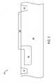
- FIG. 1Aillustrates a cross section of a portion of a conventional CMOS imager pixel 100 having a pinned photodiode 114 as its photo-conversion device.
- FIG. 1Billustrates the entire pixel 100 circuit in schematic form.
- the photodiode 114is adjacent to an isolation region 110 , which is depicted as a shallow trench isolation (STI) region.
- the photodiode 114includes an n-type region 115 underlying a p+ surface layer 116 .
- STIshallow trench isolation
- the photodiode 114converts photons to charge carriers, e.g., electrons, which are transferred to a floating diffusion region 140 by a transfer transistor 119 .
- the illustrated pixel 100typically includes a reset transistor 121 , connected to a source/drain region 136 , for resetting the floating diffusion region 140 to a predetermined level (shown as V aapix ) prior to charge transference.
- a source follower transistor 142FIG. 1B
- CMOS image sensor circuitsprocessing steps thereof, and detailed descriptions of the functions of various CMOS elements of an image sensor circuit are described, for example, in U.S. Pat. No. 6,140,630, U.S. Pat. No. 6,376,868, U.S. Pat. No. 6,310,366, U.S. Pat. No. 6,326,652, U.S. Pat. No. 6,204,524, and U.S. Pat. No. 6,333,205, assigned to Micron Technology, Inc. The disclosures of each of the forgoing patents are herein incorporated by reference in their entirety.
- CMOS sensorstypically use several transistors in every pixel for various functions including amplification.
- FIGS. 1A and 1Bdescribe a four transistor (4T) design
- pixel circuitsare also known which have fewer, (e.g., 3T), as well as more (e.g., 5T, 6T, etc.) transistors.
- 3Tthe area taken by these transistors and corresponding interconnects becomes significant and reduces the pixel area available for the photo-conversion device.
- Photo-conversion device areashould be made as large as possible to increase imager sensitivity and quantum efficiency.
- FIG. 1Aillustrates a cross-sectional view of a portion of a conventional imager pixel circuit.
- FIG. 1Billustrates a schematic view of a conventional imager pixel circuit.
- FIG. 2illustrates a cross-sectional view of an initial stage of formation of an imager pixel circuit constructed in accordance with a first embodiment.
- FIG. 3illustrates a cross-sectional view of a subsequent stage of formation of an imager pixel circuit, subsequent to what is illustrated in FIG. 2 .
- FIG. 4illustrates a cross-sectional view of a subsequent stage of formation of an imager pixel circuit, subsequent to what is illustrated in FIG. 3 .
- FIG. 5illustrates a cross-sectional view of a subsequent stage of formation of an imager pixel circuit, subsequent to what is illustrated in FIG. 4 .
- FIG. 6illustrates a cross-sectional view of a subsequent stage of formation of an imager pixel circuit, subsequent to what is illustrated in FIG. 5 .
- FIG. 6Aillustrates in schematic form another embodiment.
- FIG. 7illustrates a block diagram of an image sensor according to an embodiment.
- FIG. 8illustrates a processing system utilizing an image sensor incorporating the imager pixel circuit of the described embodiments.
- wafer and substrateare to be understood as including silicon, silicon-on-insulator (SOI) or silicon-on-sapphire (SOS) technology, doped and undoped semiconductors, and other semiconductor structures.
- SOIsilicon-on-insulator
- SOSsilicon-on-sapphire
- doped and undoped semiconductorsand other semiconductor structures.
- previous processing stepsmay have been utilized to form regions, junctions, or material layers in or over the base semiconductor structure or foundation.
- the semiconductorneed not be silicon-based, but could be based on silicon-germanium, germanium, gallium arsenide or other semiconductors.
- pixelrefers to a photo-element unit cell containing a photosensor and associated transistors for converting photons to an electrical signal.
- pixelrefers to a photo-element unit cell containing a photosensor and associated transistors for converting photons to an electrical signal.
- a single representative pixel and its manner of formationis illustrated in the figures and description herein; however, typically fabrication of a plurality of like pixels proceeds simultaneously. Accordingly, the following detailed description is not to be taken in a limiting sense, and the described embodiments are defined only by the appended claims.
- translucentas used herein, to be understood as including embodiments using translucent materials.
- the disclosed embodimentsrelate to a pixel circuit including a photo-conversion device, a floating diffusion region for receiving and storing charge from the photo-conversion device, and a transparent thin-film pixel transistor, which can be formed at least partially over the photo-conversion device while allowing image light to pass therethrough to the photo-conversion device.
- the thin-film transistormay be used as a substitute for one or more conventional pixel transistors, such as a source follower transistor, reset transistor, row select transistor, anti-blooming transistor, if used, etc., and is particularly useful as a transfer transistor for delivering stored charge from the photo-conversion device to the floating diffusion region. Methods of forming the pixel circuit are also disclosed.
- the active semiconductor material of semiconductor-on-insulator (SOI) technologieswill typically be formed as a thin film over an insulating material (typically oxide), with thicknesses of the semiconductor film being, for example, less than or equal to 2000 ⁇ .
- insulating materialtypically oxide
- bulk semiconductor materialwill typically have a thickness of at least about 200 microns.
- the thin semiconductor of SOI technologycan allow higher performance and lower power consumption to be achieved in integrated circuits than can be achieved with similar circuits utilizing bulk materials.
- An integrated circuit device that can be formed utilizing SOI technologiesincludes a so-called thin film transistor (TFT), with the term “thin film” referring to the thin semiconductor film of the SOI construction.
- the semiconductor material of the SOI constructioncan be silicon, and, as such, the TFTs can be fabricated using recrystallized amorphous silicon or polycrystalline silicon.
- the siliconcan be supported by an electrically insulative material (such as silicon dioxide), which in turn is supported by an appropriate substrate.
- the semiconductor materialcomprises silicon
- SOIis occasionally utilized to refer to a silicon-on-insulator construction, rather than the more general concept of a semiconductor-on-insulator construction.
- SOIrefers to semiconductor-on-insulator constructions. Accordingly, the semiconductor material of an SOI construction referred to in the context of this disclosure can comprise other semiconductive materials in addition to, or alternatively to, silicon.
- FIG. 2illustrates a cross-sectional view of an initial stage of formation of an imager pixel circuit 200 constructed in accordance with one embodiment where the transistor formed is a transfer transistor for a pixel circuit.
- the pixel circuit 200includes a silicon (Si) substrate 205 of a first conductivity type; an STI region 210 , which is formed in the substrate 205 and surrounds and isolates a pixel.
- the STI region 210is filled with a dielectric material.
- a doped region 215 of a second conductivity typeis formed in the substrate 205 , and which will become part of a photo-conversion device 214 ( FIG.
- photo-conversion device 214( FIG. 3 ) is a pinned photodiode.
- the first conductivity typeis p-type, and the second conductivity type is n-type.
- photo-conversion device 214( FIG. 3 ) may extend into the substrate 205 to a depth of about 1 ⁇ m.
- FIG. 3illustrates a cross-sectional view of a subsequent stage of formation of the imager pixel circuit 200 .
- a doped surface layer 216 for a photo-conversion device 214is implanted.
- Doped surface layer 216is doped to the first conductivity type.
- doped surface layer 216is a highly doped p+ surface layer and is formed to a depth of approximately 0.1 ⁇ m.
- a p-type dopant, such as boron, indium, or any other suitable p-type dopant,may be used to form the p+ surface layer 216 .
- a layer of zinc tin oxide (ZTO) 225is formed over a portion of the STI region 210 , doped regions 215 , 216 , and part of SiO 2 layer 220 .
- the ZTO layer 225is transparent to visible high-frequency light at short wavelengths and near ultraviolet, as well as to all visible wavelengths, and is a semiconductor material which will form an effective second selectively conductive channel for a transfer transistor 219 ( FIG. 6 ), as discussed below.
- the p-type dopantmay be incorporated into the ZTO layer 225 during deposition (in-situ doped ZTO) or afterward.
- ZTO thin filmshave broad direct optical band gap characteristic in the range of 3.3 to 3.9 eV. This is due to a large Burstein-Moss shift in this material. The Burstein-Moss effect is conduction band filling with an increased free electron concentration.
- ZTOalso has useful properties, including chemical stability with respect to oxidation and etching, and physical robustness. Carrier mobility in ZTO is one of the best among known transparent metallic oxides, and therefore high ratios of on and off currents are possible with ZTO, relative to other transparent metallic oxide gate material based transistors.
- Part of the ZTO layer 225is used as a channel region for a transistor of the pixel.
- Source/drain regions 281can be formed in the ZTO layer 225 by conventional doping, preferably with very low Schottky barriers. Alternatively, source/drain regions 281 can be formed on the ZTO layer 225 by direct metal deposition.
- FIG. 4illustrates a cross-sectional view of a subsequent stage of formation of the imager pixel circuit 200 .
- a transparent dielectric layer 230is formed over part of ZTO layer 225 .
- Dielectric layer 230is typically constructed of a material such as aluminum oxide (Al 2 O 3 ), tin oxide (TiO 3 ), or atomic layer deposition silicon dioxide (ALD SiO 2 ).
- FIG. 5illustrates a cross-sectional view of a subsequent stage of formation of the imager pixel circuit 200 .
- a transfer gate electrode 240is formed over at least part of dielectric layer 230 .
- a reset gate electrode 241 for reset transistor 221is formed over part of the SiO 2 layer 220 .
- the transfer gate electrode 240may be any suitable conductive material, preferably one that is transparent to radiant energy, including but not limited to doped polysilicon or a transparent material such as indium tin oxide (ITO).
- ITOindium tin oxide
- the transfer gate electrode 240may cover part or all of the dielectric layer 230 .
- the use of a transparent materials for transfer transistor 219allows transfer transistor 219 ( FIG.
- Embodimentsinclude a thickness range of about 100 ⁇ to 2500 ⁇ for ZTO layer 225 , about 50 ⁇ to 300 ⁇ for dielectric layer 230 , and about 500 ⁇ to 1000 ⁇ for transfer gate electrode 240 .
- the thickness of ZTO layer 225may be altered for different applications. For example, thinner to reduce absorption loss, and thicker for planarization.
- “Fill factor”is a measure of the size of a light sensitive region in a photodiode relative to the surface area of the pixel. In Active Pixel Sensor (APS) technology, each pixel includes transistors that form active circuits.
- these transistorsare not light sensitive regions and therefore reduce the fill factor of a pixel since they take space (surface area) which otherwise could be used for increasing the area of the photodiode.
- a floating diffusion region 245 and a source/drain region 251 of the reset transistor 221may be implanted by known methods, including a plasma-assisted doping (PLAD) process.
- the floating diffusion region 245 and source/drain region 251 of the reset transistor 221are formed as regions of the second conductivity type, which, in this example, is n-type. Any suitable n-type dopant, such as phosphorus, arsenic, or antimony, may be used.
- the floating diffusion region 245is formed between the transfer transistor 219 ( FIG. 6 ) gate stack and the reset transistor 221 gate stack.
- the source/drain region 251 of the reset transistor 221is formed between the reset transistor 221 and the second STI region 211 .
- the floating diffusion region 245stores charge collected from the photo-conversion device 214 , through a first channel between doped region 215 and the floating diffusion region 245 , under the SiO 2 layer 220 , which functions as a dielectric.
- FIG. 6illustrates a cross-sectional view of a subsequent stage of formation of the imager pixel circuit 200 constructed in accordance with the described embodiments.
- the transfer transistor 219 gate stackincludes, at this point, the SiO 2 layer 220 , the ZTO layer 225 , the dielectric layer 230 , and the transfer gate electrode 240 .
- the reset transistor 221 gate stackincludes, at this point, the SiO 2 layer 220 , and the reset gate electrode 241 .
- Sidewalls 255 and a top cap layer 256are formed on each gate stack, typically by an oxide growth, followed by, for example, a dry etch process or by material deposition and etch back.
- a source/drain region 281 in ZTO layer 225is connected to the floating diffusion region 245 through several possible schemes, enabling the ZTO layer 225 to function as a second channel for the transfer transistor 219 .
- Such schemesinclude (1) an interconnect process through metallization and contacts connecting floating diffusion region 245 to line 260 ; (2) a local interconnect process using silicidation; and (3) butted contact connecting floating diffusion region 245 to line 260 through a conducting spacer. Therefore, transfer transistor 219 has two channels that function to transfer charge from photo-conversion device 214 upon application of a gate control signal on gate electrode 240 : the region of substrate 205 between doped region 215 and the floating diffusion region 245 , and the ZTO layer 225 between source/drain regions 281 .
- Charge collected in the photo-conversion device 214may reach the ZTO layer 225 by carrier drift, as an electric field exists in ZTO layer 225 , or through diffusion (for, e.g., red photons).
- the source/drain region 251 of the reset transistor 221is connected to a pixel supply voltage V aapix , enabling reset transistor 221 to reset the floating diffusion region 245 .
- a readout circuit 600(shown in schematic form) is connected to the floating diffusion region 245 via line 260 .
- the readout circuit 600includes a source follower transistor 610 , having a gate connected to the floating diffusion region 245 through line 260 , and a first source/drain region connected to the pixel supply voltage V aapix .
- the readout circuit 600also includes a row select transistor 620 for selecting the pixel 200 for readout in response to a signal received at the gate of the row select transistor 620 .
- the row select transistor 620has a first source/drain region connected to a second source/drain region of the source follower transistor 610 , and a second source/drain region connected to an array column output line.
- the embodiment illustratedprovides a transparent thin film transistor (TFT) for the transfer transistor which may be provided partially or wholly over the photo-conversion device 214 .
- TFTtransparent thin film transistor
- Conventional processing methodsmay be used to complete the pixel 200 .
- insulating, shielding, and metallization layers to connect gate lines, and other connections to the pixel 200may be formed.
- the entire surfacemay be covered with a passivation layer (not shown) of, for example, silicon dioxide, BSG, PSG, or BPSG, which is CMP planarized and etched to provide contact holes, which are then metallized to provide contacts.
- Conventional layers of conductors and insulatorsmay also be used to interconnect the structures and to connect pixel 200 to peripheral circuitry.
- any one or more of the transfer transistor 219 , reset transistor 221 , source follower transistor 610 and row select transistor 620may be constructed as a TFT in the manner illustrated in the embodiment with respect to transistor elements 225 , 230 , 240 , 255 , 256 , 281 , and be provided partially or wholly over the photo-conversion device 214 .
- the embodimentsmay be employed in pixels having fewer or more transistors than illustrated in FIG. 6 .
- any or all of the pixel transistorsmay be constructed as described above with respect to transfer transistor 219 .
- some pixelsemploy an anti-blooming transistor 343 and/or storage gate transistors 345 , which are coupled to the photo-conversion device 214 .
- These, too,may be formed as TFT transistors in the manner described above, and be placed partially or wholly over the photo-conversion device 214 .
- the described embodimentsincrease the fill factor by having transistors which are transparent to visible light and/or to high-frequency and near ultra-violet light, formed over at least a portion of the photo-conversion device 214 , and improves the quantum efficiency in scaled pixels.
- Embodimentsinclude less than 10% signal loss due to scattering, although, amounts of translucency may be offset by gains of other means, such as increased fill factor.
- Thin, transparent TFT channelsare constructed on silicon-dioxide films for specific transistors in the pixel.
- the channel regionis made out of transparent material so that they can be directly placed on top of photo-conversion devices, such as a photo-conversion device 214 , enabling improvement in fill factor and quantum efficiency.
- photo-conversion devicessuch as a photo-conversion device 214
- only a part of the transistoris transparent, including parts other than the gate stack.
- anti-reflective (AR) filmson top of the ITO or ZTO layer to reduce reflections at the top interface.
- pixels constructed in accordance with the emodimentsmay be formed as part of an image sensor having a array of pixels.
- FIG. 7illustrates a single chip CMOS image sensor 1100 which has a pixel array 1111 containing a plurality of pixel cells arranged in rows and columns.
- the array 1111includes one or more pixels 200 constructed as described above in connection with FIGS. 2-6A .
- the pixels of each row in array 1111are all turned on at the same time by a row select line, and the pixel signals of each column are selectively output onto column readout lines by respective column select lines.
- the row linesare selectively activated by a row driver 1151 in response to row address decoder 1150 .
- the column select linesare selectively activated by a column driver 1153 in response to column address decoder 1154 .
- the pixel arrayis operated by the timing and control circuit 1152 , which controls address decoders 1150 , 1154 for selecting the appropriate row and column lines for pixel signal readout.
- the signals on the column readout linestypically include a pixel reset signal (V rst ) and a pixel image signal (V photo ) for each pixel. Both signals are read into a sample and hold circuit (S/H) 1155 associated with the column driver 1153 .
- a differential signal (V rst -V photo )is produced by differential amplifier (AMP) 1156 for each pixel, and each pixel's differential signal is amplified and digitized by analog-to-digital converter (ADC) 1157 .
- ADCanalog-to-digital converter
- the analog-to-digital converter 1157supplies the digitized pixel signals to an image processor 1158 , which performs appropriate image processing before outputting digital signals defining an image.
- FIG. 8illustrates a processor system 500 , for example a still or video camera system, which generally comprises a central processing unit (CPU) 505 , such as a microprocessor for controlling camera functions, that communicates with one or more input/output (I/O) devices 510 over a bus 515 .
- Imager 1100also communicates with the CPU 505 over bus 515 .
- the system 500also includes random access memory (RAM) 520 , and can include removable memory 525 , such as flash memory, which also communicate with CPU 505 over the bus 515 .
- Imager 1100may be combined with a processor, such as a CPU, digital signal processor, or microprocessor, with or without memory storage on a single integrated circuit or on a different chip than the processor.
- the processor system 500is an example of a system having digital circuits that could include image sensor devices. Without being limiting, such a system could include a computer system, camera system, scanner, machine vision, vehicle navigation, video phone, surveillance system, auto focus system, star tracker system, motion detection system, image stabilization system, and data compression system.
- pnp-type pinned photodiodeWhile the above embodiments are described in connection with the formation of an pnp-type pinned photodiode, the embodiments are not limited thereto. There is also applicability to other types of photo-conversion devices or photosensors for charge generation, such as a photodiode formed from np or npn regions in a substrate, a photogate, or a photoconductor. If an npn-type photodiode is formed the dopant and conductivity types of all structures would change accordingly.
- the embodimentshave been illustrated in the environment of a four transistor (4T) pixel, it should be appreciated that the embodiments are not so limited and the pixel circuit 200 can be implemented in a design with either a higher or lower number of transistors with or without the presence of a transfer transistor. The embodiments may also be used in pixels of other solid state arrays.
Landscapes
- Solid State Image Pick-Up Elements (AREA)
- Thin Film Transistor (AREA)
Abstract
Description
- Disclosed embodiments relate to the field of semiconductor devices, particularly to image sensors using thin film technology.
- Typically, an image sensor array includes a focal plane array of pixels, each one of the pixels including a photo-conversion device such as, e.g., a photogate, photoconductor, or a photodiode.
FIG. 1A illustrates a cross section of a portion of a conventionalCMOS imager pixel 100 having a pinnedphotodiode 114 as its photo-conversion device.FIG. 1B illustrates theentire pixel 100 circuit in schematic form. Thephotodiode 114 is adjacent to anisolation region 110, which is depicted as a shallow trench isolation (STI) region. Thephotodiode 114 includes an n-type region 115 underlying ap+ surface layer 116. - The
photodiode 114 converts photons to charge carriers, e.g., electrons, which are transferred to afloating diffusion region 140 by atransfer transistor 119. In addition, the illustratedpixel 100 typically includes areset transistor 121, connected to a source/drain region 136, for resetting thefloating diffusion region 140 to a predetermined level (shown as Vaapix) prior to charge transference. In operation, a source follower transistor142 (FIG. 1B ) outputs a voltage representing the charge on thefloating diffusion region 140 to a column line150 (FIG. 1B ) when a row select transistor152 (FIG. 1B ) for the row containing thepixel 100 is activated. - CMOS image sensor circuits, processing steps thereof, and detailed descriptions of the functions of various CMOS elements of an image sensor circuit are described, for example, in U.S. Pat. No. 6,140,630, U.S. Pat. No. 6,376,868, U.S. Pat. No. 6,310,366, U.S. Pat. No. 6,326,652, U.S. Pat. No. 6,204,524, and U.S. Pat. No. 6,333,205, assigned to Micron Technology, Inc. The disclosures of each of the forgoing patents are herein incorporated by reference in their entirety.
- In the
conventional pixel 100, when incident light strikes the surface of thephotodiode 114, charge carriers (electrons), are generated in the depletion region of the p-n junction (betweenregion 115 and region116) of thephotodiode 114. - As can be seen from
FIGS. 1A and 1B , CMOS sensors typically use several transistors in every pixel for various functions including amplification. AlthoughFIGS. 1A and 1B describe a four transistor (4T) design, pixel circuits are also known which have fewer, (e.g., 3T), as well as more (e.g., 5T, 6T, etc.) transistors. As pixel size is scaled down in high-resolution sensors, the area taken by these transistors and corresponding interconnects becomes significant and reduces the pixel area available for the photo-conversion device. Photo-conversion device area should be made as large as possible to increase imager sensitivity and quantum efficiency. - In addition, there are several imaging applications that require high quantum efficiency, small pixels, and have unique wavelength requirements, such as shorter visible wavelengths and ultraviolet light. Increasing the size of the photo-conversion device area is particularly important in such cases.
FIG. 1A illustrates a cross-sectional view of a portion of a conventional imager pixel circuit.FIG. 1B illustrates a schematic view of a conventional imager pixel circuit.FIG. 2 illustrates a cross-sectional view of an initial stage of formation of an imager pixel circuit constructed in accordance with a first embodiment.FIG. 3 illustrates a cross-sectional view of a subsequent stage of formation of an imager pixel circuit, subsequent to what is illustrated inFIG. 2 .FIG. 4 illustrates a cross-sectional view of a subsequent stage of formation of an imager pixel circuit, subsequent to what is illustrated inFIG. 3 .FIG. 5 illustrates a cross-sectional view of a subsequent stage of formation of an imager pixel circuit, subsequent to what is illustrated inFIG. 4 .FIG. 6 illustrates a cross-sectional view of a subsequent stage of formation of an imager pixel circuit, subsequent to what is illustrated inFIG. 5 .FIG. 6A illustrates in schematic form another embodiment.FIG. 7 illustrates a block diagram of an image sensor according to an embodiment.FIG. 8 illustrates a processing system utilizing an image sensor incorporating the imager pixel circuit of the described embodiments.- In the following detailed description, reference is made to the accompanying drawings, which form a part hereof and show by way of illustration specific embodiments in which the invention may be practiced. These embodiments are described in sufficient detail to enable those skilled in the art to practice them, and it is to be understood that other embodiments may be utilized, and that structural, logical, processing, and electrical changes may be made. The progression of processing steps described is an example; however, the sequence of steps is not limited to that set forth herein and may be changed as is known in the art, with the exception of steps necessarily occurring in a certain order.
- The terms “wafer” and “substrate,” as used herein, are to be understood as including silicon, silicon-on-insulator (SOI) or silicon-on-sapphire (SOS) technology, doped and undoped semiconductors, and other semiconductor structures. Furthermore, when reference is made to a “wafer” or “substrate” in the following description, previous processing steps may have been utilized to form regions, junctions, or material layers in or over the base semiconductor structure or foundation. In addition, the semiconductor need not be silicon-based, but could be based on silicon-germanium, germanium, gallium arsenide or other semiconductors.
- The term “pixel,” as used herein, refers to a photo-element unit cell containing a photosensor and associated transistors for converting photons to an electrical signal. For purposes of illustration, a single representative pixel and its manner of formation is illustrated in the figures and description herein; however, typically fabrication of a plurality of like pixels proceeds simultaneously. Accordingly, the following detailed description is not to be taken in a limiting sense, and the described embodiments are defined only by the appended claims.
- The term “transparent,” as used herein, to be understood as including embodiments using translucent materials.
- The disclosed embodiments relate to a pixel circuit including a photo-conversion device, a floating diffusion region for receiving and storing charge from the photo-conversion device, and a transparent thin-film pixel transistor, which can be formed at least partially over the photo-conversion device while allowing image light to pass therethrough to the photo-conversion device. The thin-film transistor may be used as a substitute for one or more conventional pixel transistors, such as a source follower transistor, reset transistor, row select transistor, anti-blooming transistor, if used, etc., and is particularly useful as a transfer transistor for delivering stored charge from the photo-conversion device to the floating diffusion region. Methods of forming the pixel circuit are also disclosed.
- The active semiconductor material of semiconductor-on-insulator (SOI) technologies will typically be formed as a thin film over an insulating material (typically oxide), with thicknesses of the semiconductor film being, for example, less than or equal to 2000 Å. In contrast, bulk semiconductor material will typically have a thickness of at least about 200 microns. The thin semiconductor of SOI technology can allow higher performance and lower power consumption to be achieved in integrated circuits than can be achieved with similar circuits utilizing bulk materials.
- An integrated circuit device that can be formed utilizing SOI technologies includes a so-called thin film transistor (TFT), with the term “thin film” referring to the thin semiconductor film of the SOI construction. In particular, the semiconductor material of the SOI construction can be silicon, and, as such, the TFTs can be fabricated using recrystallized amorphous silicon or polycrystalline silicon. The silicon can be supported by an electrically insulative material (such as silicon dioxide), which in turn is supported by an appropriate substrate. If the semiconductor material comprises silicon, the term SOI is occasionally utilized to refer to a silicon-on-insulator construction, rather than the more general concept of a semiconductor-on-insulator construction. However, it is to be understood that in the context of this disclosure the term SOI refers to semiconductor-on-insulator constructions. Accordingly, the semiconductor material of an SOI construction referred to in the context of this disclosure can comprise other semiconductive materials in addition to, or alternatively to, silicon.
- Now referring to the figures, where like numerals designate like elements,
FIG. 2 illustrates a cross-sectional view of an initial stage of formation of animager pixel circuit 200 constructed in accordance with one embodiment where the transistor formed is a transfer transistor for a pixel circuit. Thepixel circuit 200 includes a silicon (Si)substrate 205 of a first conductivity type; anSTI region 210, which is formed in thesubstrate 205 and surrounds and isolates a pixel. TheSTI region 210 is filled with a dielectric material. A dopedregion 215 of a second conductivity type is formed in thesubstrate 205, and which will become part of a photo-conversion device214 (FIG. 3 ) and a silicon dioxide (SiO2)layer 220 is formed on thesubstrate 205, for example, by a strip/regrow process. In this example, photo-conversion device214 (FIG. 3 ) is a pinned photodiode. Also in this example, the first conductivity type is p-type, and the second conductivity type is n-type. Typically, photo-conversion device214 (FIG. 3 ) may extend into thesubstrate 205 to a depth of about 1 μm. FIG. 3 illustrates a cross-sectional view of a subsequent stage of formation of theimager pixel circuit 200. A dopedsurface layer 216 for a photo-conversion device 214 is implanted. Dopedsurface layer 216 is doped to the first conductivity type. Illustratively, dopedsurface layer 216 is a highly doped p+ surface layer and is formed to a depth of approximately 0.1 μm. A p-type dopant, such as boron, indium, or any other suitable p-type dopant, may be used to form thep+ surface layer 216. A layer of zinc tin oxide (ZTO)225 is formed over a portion of theSTI region 210, dopedregions ZTO layer 225 is transparent to visible high-frequency light at short wavelengths and near ultraviolet, as well as to all visible wavelengths, and is a semiconductor material which will form an effective second selectively conductive channel for a transfer transistor219 (FIG. 6 ), as discussed below. Optionally, the p-type dopant may be incorporated into theZTO layer 225 during deposition (in-situ doped ZTO) or afterward.- ZTO thin films have broad direct optical band gap characteristic in the range of 3.3 to 3.9 eV. This is due to a large Burstein-Moss shift in this material. The Burstein-Moss effect is conduction band filling with an increased free electron concentration. ZTO also has useful properties, including chemical stability with respect to oxidation and etching, and physical robustness. Carrier mobility in ZTO is one of the best among known transparent metallic oxides, and therefore high ratios of on and off currents are possible with ZTO, relative to other transparent metallic oxide gate material based transistors. Part of the
ZTO layer 225 is used as a channel region for a transistor of the pixel. Source/drain regions 281 can be formed in theZTO layer 225 by conventional doping, preferably with very low Schottky barriers. Alternatively, source/drain regions 281 can be formed on theZTO layer 225 by direct metal deposition. FIG. 4 illustrates a cross-sectional view of a subsequent stage of formation of theimager pixel circuit 200. Atransparent dielectric layer 230 is formed over part ofZTO layer 225.Dielectric layer 230 is typically constructed of a material such as aluminum oxide (Al2O3), tin oxide (TiO3), or atomic layer deposition silicon dioxide (ALD SiO2).FIG. 5 illustrates a cross-sectional view of a subsequent stage of formation of theimager pixel circuit 200. Atransfer gate electrode 240 is formed over at least part ofdielectric layer 230. Areset gate electrode 241 forreset transistor 221 is formed over part of the SiO2layer220. Thetransfer gate electrode 240 may be any suitable conductive material, preferably one that is transparent to radiant energy, including but not limited to doped polysilicon or a transparent material such as indium tin oxide (ITO). Thetransfer gate electrode 240 may cover part or all of thedielectric layer 230. The use of a transparent materials fortransfer transistor 219 allows transfer transistor219 (FIG. 6 ) to be directly placed over at least a portion of photo-conversion device 214 It may also be placed entirely over the photo-conversion device 214, providing drastic improvement in fill factor and quantum efficiency. Embodiments include a thickness range of about 100 Å to 2500 Å forZTO layer 225, about 50 Å to 300 Å fordielectric layer 230, and about 500 Å to 1000 Å fortransfer gate electrode 240. The thickness ofZTO layer 225 may be altered for different applications. For example, thinner to reduce absorption loss, and thicker for planarization. “Fill factor” is a measure of the size of a light sensitive region in a photodiode relative to the surface area of the pixel. In Active Pixel Sensor (APS) technology, each pixel includes transistors that form active circuits.- Generally, these transistors are not light sensitive regions and therefore reduce the fill factor of a pixel since they take space (surface area) which otherwise could be used for increasing the area of the photodiode.
- A floating
diffusion region 245 and a source/drain region 251 of the reset transistor221 (FIG. 6 ) may be implanted by known methods, including a plasma-assisted doping (PLAD) process. The floatingdiffusion region 245 and source/drain region 251 of thereset transistor 221 are formed as regions of the second conductivity type, which, in this example, is n-type. Any suitable n-type dopant, such as phosphorus, arsenic, or antimony, may be used. The floatingdiffusion region 245 is formed between the transfer transistor219 (FIG. 6 ) gate stack and thereset transistor 221 gate stack. The source/drain region 251 of thereset transistor 221 is formed between thereset transistor 221 and the second STI region211. The floatingdiffusion region 245 stores charge collected from the photo-conversion device 214, through a first channel between dopedregion 215 and the floatingdiffusion region 245, under the SiO2layer220, which functions as a dielectric. FIG. 6 illustrates a cross-sectional view of a subsequent stage of formation of theimager pixel circuit 200 constructed in accordance with the described embodiments. Thetransfer transistor 219 gate stack includes, at this point, the SiO2layer220, theZTO layer 225, thedielectric layer 230, and thetransfer gate electrode 240. Thereset transistor 221 gate stack includes, at this point, the SiO2layer220, and thereset gate electrode 241.Sidewalls 255 and atop cap layer 256 are formed on each gate stack, typically by an oxide growth, followed by, for example, a dry etch process or by material deposition and etch back. A source/drain region 281 inZTO layer 225 is connected to the floatingdiffusion region 245 through several possible schemes, enabling theZTO layer 225 to function as a second channel for thetransfer transistor 219. Such schemes include (1) an interconnect process through metallization and contacts connecting floatingdiffusion region 245 toline 260; (2) a local interconnect process using silicidation; and (3) butted contact connecting floatingdiffusion region 245 toline 260 through a conducting spacer. Therefore,transfer transistor 219 has two channels that function to transfer charge from photo-conversion device 214 upon application of a gate control signal on gate electrode240: the region ofsubstrate 205 between dopedregion 215 and the floatingdiffusion region 245, and theZTO layer 225 between source/drain regions 281. Charge collected in the photo-conversion device 214 may reach theZTO layer 225 by carrier drift, as an electric field exists inZTO layer 225, or through diffusion (for, e.g., red photons). The source/drain region 251 of thereset transistor 221 is connected to a pixel supply voltage Vaapix, enablingreset transistor 221 to reset the floatingdiffusion region 245.- A readout circuit600 (shown in schematic form) is connected to the floating
diffusion region 245 vialine 260. Thereadout circuit 600 includes asource follower transistor 610, having a gate connected to the floatingdiffusion region 245 throughline 260, and a first source/drain region connected to the pixel supply voltage Vaapix. Thereadout circuit 600 also includes a rowselect transistor 620 for selecting thepixel 200 for readout in response to a signal received at the gate of the rowselect transistor 620. The rowselect transistor 620 has a first source/drain region connected to a second source/drain region of thesource follower transistor 610, and a second source/drain region connected to an array column output line. - The embodiment illustrated provides a transparent thin film transistor (TFT) for the transfer transistor which may be provided partially or wholly over the photo-
conversion device 214. Conventional processing methods may be used to complete thepixel 200. For example, insulating, shielding, and metallization layers to connect gate lines, and other connections to thepixel 200 may be formed. Also, the entire surface may be covered with a passivation layer (not shown) of, for example, silicon dioxide, BSG, PSG, or BPSG, which is CMP planarized and etched to provide contact holes, which are then metallized to provide contacts. Conventional layers of conductors and insulators may also be used to interconnect the structures and to connectpixel 200 to peripheral circuitry. - In addition, other transistors within a pixel circuit may also be constructed in the manner described above for the
transfer transistor 219. Using the illustrated four transistor pixel shown inFIG. 6 , any one or more of thetransfer transistor 219,reset transistor 221,source follower transistor 610 and rowselect transistor 620 may be constructed as a TFT in the manner illustrated in the embodiment with respect totransistor elements conversion device 214. - Also, the embodiments may be employed in pixels having fewer or more transistors than illustrated in
FIG. 6 . As should be apparent, any or all of the pixel transistors may be constructed as described above with respect to transfertransistor 219. For example, as illustrated inFIG. 6A , some pixels employ ananti-blooming transistor 343 and/orstorage gate transistors 345, which are coupled to the photo-conversion device 214. These, too, may be formed as TFT transistors in the manner described above, and be placed partially or wholly over the photo-conversion device 214. The described embodiments increase the fill factor by having transistors which are transparent to visible light and/or to high-frequency and near ultra-violet light, formed over at least a portion of the photo-conversion device 214, and improves the quantum efficiency in scaled pixels. Embodiments include less than 10% signal loss due to scattering, although, amounts of translucency may be offset by gains of other means, such as increased fill factor. - Thin, transparent TFT channels are constructed on silicon-dioxide films for specific transistors in the pixel. The channel region is made out of transparent material so that they can be directly placed on top of photo-conversion devices, such as a photo-
conversion device 214, enabling improvement in fill factor and quantum efficiency. There are also embodiments in which only a part of the transistor is transparent, including parts other than the gate stack. Techniques exist which may increase transmission (i.e., reduce loss in film) in ITO and ZTO materials. Typically, changing the stoichiometry of the constituent elements in these films may change the transmission coefficient. Also, by incorporating rare-earth elements, such as erbium, optical loss can be reduced further. There are also other techniques, such as placing anti-reflective (AR) films on top of the ITO or ZTO layer to reduce reflections at the top interface. - As illustrated in
FIG. 7 , pixels constructed in accordance with the emodiments may be formed as part of an image sensor having a array of pixels.FIG. 7 illustrates a single chipCMOS image sensor 1100 which has apixel array 1111 containing a plurality of pixel cells arranged in rows and columns. Thearray 1111 includes one ormore pixels 200 constructed as described above in connection withFIGS. 2-6A . - The pixels of each row in
array 1111 are all turned on at the same time by a row select line, and the pixel signals of each column are selectively output onto column readout lines by respective column select lines. The row lines are selectively activated by arow driver 1151 in response torow address decoder 1150. The column select lines are selectively activated by acolumn driver 1153 in response tocolumn address decoder 1154. The pixel array is operated by the timing andcontrol circuit 1152, which controlsaddress decoders - The signals on the column readout lines typically include a pixel reset signal (Vrst) and a pixel image signal (Vphoto) for each pixel. Both signals are read into a sample and hold circuit (S/H)1155 associated with the
column driver 1153. A differential signal (Vrst-Vphoto) is produced by differential amplifier (AMP)1156 for each pixel, and each pixel's differential signal is amplified and digitized by analog-to-digital converter (ADC)1157. The analog-to-digital converter 1157 supplies the digitized pixel signals to animage processor 1158, which performs appropriate image processing before outputting digital signals defining an image. Although the embodiments are described in connection with aCMOS image sensor 1100, the embodiments are also applicable to analogous structures of a charge coupled device (CCD) image sensor. FIG. 8 illustrates aprocessor system 500, for example a still or video camera system, which generally comprises a central processing unit (CPU)505, such as a microprocessor for controlling camera functions, that communicates with one or more input/output (I/O)devices 510 over abus 515.Imager 1100 also communicates with theCPU 505 overbus 515. Thesystem 500 also includes random access memory (RAM)520, and can includeremovable memory 525, such as flash memory, which also communicate withCPU 505 over thebus 515.Imager 1100 may be combined with a processor, such as a CPU, digital signal processor, or microprocessor, with or without memory storage on a single integrated circuit or on a different chip than the processor.- The
processor system 500 is an example of a system having digital circuits that could include image sensor devices. Without being limiting, such a system could include a computer system, camera system, scanner, machine vision, vehicle navigation, video phone, surveillance system, auto focus system, star tracker system, motion detection system, image stabilization system, and data compression system. - While the above embodiments are described in connection with the formation of an pnp-type pinned photodiode, the embodiments are not limited thereto. There is also applicability to other types of photo-conversion devices or photosensors for charge generation, such as a photodiode formed from np or npn regions in a substrate, a photogate, or a photoconductor. If an npn-type photodiode is formed the dopant and conductivity types of all structures would change accordingly. In addition, although the embodiments have been illustrated in the environment of a four transistor (4T) pixel, it should be appreciated that the embodiments are not so limited and the
pixel circuit 200 can be implemented in a design with either a higher or lower number of transistors with or without the presence of a transfer transistor. The embodiments may also be used in pixels of other solid state arrays. - The processes and devices in the above description and drawings illustrate examples of methods and devices of many that could be used and produced to achieve the objects, features, and advantages of embodiments described herein. For example, the described embodiments may be used in a digital camera, a video camera, or any other device employing image pixels. Thus, they are not to be seen as limited by the foregoing description of the embodiments, but only limited by the appended claims.
Claims (68)
Priority Applications (7)
| Application Number | Priority Date | Filing Date | Title |
|---|---|---|---|
| US11/513,242US7663165B2 (en) | 2006-08-31 | 2006-08-31 | Transparent-channel thin-film transistor-based pixels for high-performance image sensors |
| JP2009507860AJP2009535819A (en) | 2006-08-31 | 2007-08-28 | Transparent channel thin film transistor based pixels for high performance image sensors |
| EP07811565AEP2057684A2 (en) | 2006-08-31 | 2007-08-28 | Stacked transparent-dual-channel thin-film transistor-based pixels for cmos image sensors |
| KR1020087014652AKR101003869B1 (en) | 2006-08-31 | 2007-08-28 | Transparent channel thin film transistor based pixels for high performance image sensors |
| PCT/US2007/018934WO2008027392A2 (en) | 2006-08-31 | 2007-08-28 | Stacked transparent-dual-channel thin-film transistor-based pixels for cmos image sensors |
| CNA2007800017532ACN101366120A (en) | 2006-08-31 | 2007-08-28 | Transparent-channel thin-film transistor-based pixels for high-performance image sensors |
| TW096132644ATW200824108A (en) | 2006-08-31 | 2007-08-31 | Transparent-channel thin-film transistor-based pixels for high-performance image sensors |
Applications Claiming Priority (1)
| Application Number | Priority Date | Filing Date | Title |
|---|---|---|---|
| US11/513,242US7663165B2 (en) | 2006-08-31 | 2006-08-31 | Transparent-channel thin-film transistor-based pixels for high-performance image sensors |
Publications (2)
| Publication Number | Publication Date |
|---|---|
| US20080054319A1true US20080054319A1 (en) | 2008-03-06 |
| US7663165B2 US7663165B2 (en) | 2010-02-16 |
Family
ID=39136545
Family Applications (1)
| Application Number | Title | Priority Date | Filing Date |
|---|---|---|---|
| US11/513,242Active2028-09-25US7663165B2 (en) | 2006-08-31 | 2006-08-31 | Transparent-channel thin-film transistor-based pixels for high-performance image sensors |
Country Status (7)
| Country | Link |
|---|---|
| US (1) | US7663165B2 (en) |
| EP (1) | EP2057684A2 (en) |
| JP (1) | JP2009535819A (en) |
| KR (1) | KR101003869B1 (en) |
| CN (1) | CN101366120A (en) |
| TW (1) | TW200824108A (en) |
| WO (1) | WO2008027392A2 (en) |
Cited By (50)
| Publication number | Priority date | Publication date | Assignee | Title |
|---|---|---|---|---|
| US20090101948A1 (en)* | 2007-10-19 | 2009-04-23 | Samsung Electronics Co., Ltd. | CMOS image sensors having transparent transistors and methods of manufacturing the same |
| US20100019239A1 (en)* | 2008-07-23 | 2010-01-28 | Electronics And Telecommunications Research Institute | Method of fabricating zto thin film, thin film transistor employing the same, and method of fabricating thin film transistor |
| US20100193785A1 (en)* | 2007-06-29 | 2010-08-05 | Semiconductor Energy Laboratory Co., Ltd. | Semiconductor device |
| US20110001136A1 (en)* | 2007-11-15 | 2011-01-06 | Sumitomo Chemical Company, Limited | Oxide semiconductor material, method for manufacturing oxide semiconductor material, electronic device and field effect transistor |
| US20110089975A1 (en)* | 2009-10-16 | 2011-04-21 | Semiconductor Energy Laboratory Co., Ltd. | Logic circuit and semiconductor device |
| US20110108836A1 (en)* | 2009-11-06 | 2011-05-12 | Semiconductor Energy Laboratory Co., Ltd. | Semiconductor device |
| US20110108706A1 (en)* | 2009-11-06 | 2011-05-12 | Semiconductor Energy Laboratory Co., Ltd. | Semiconductor device and operating method thereof |
| US20110108704A1 (en)* | 2009-11-11 | 2011-05-12 | Samsung Electronics Co., Ltd. | Image sensors and methods of operating the same |
| US20110176038A1 (en)* | 2010-01-15 | 2011-07-21 | Semiconductor Energy Laboratory Co., Ltd. | Semiconductor device and method for driving the same |
| US20110198483A1 (en)* | 2010-02-12 | 2011-08-18 | Semiconductor Energy Laboratory Co., Ltd. | Semiconductor device and driving method thereof |
| WO2011102183A1 (en)* | 2010-02-19 | 2011-08-25 | Semiconductor Energy Laboratory Co., Ltd. | Semiconductor device |
| US20110215323A1 (en)* | 2010-03-08 | 2011-09-08 | Semiconductor Energy Laboratory Co., Ltd. | Semiconductor device and manufacturing method thereof |
| US20110221723A1 (en)* | 2010-03-12 | 2011-09-15 | Semiconductor Energy Laboratory Co., Ltd. | Driving method of display device |
| US20110220889A1 (en)* | 2010-03-12 | 2011-09-15 | Semiconductor Energy Laboratory Co., Ltd. | Semiconductor device |
| JP2012039059A (en)* | 2009-12-28 | 2012-02-23 | Semiconductor Energy Lab Co Ltd | Semiconductor device |
| JP2012039058A (en)* | 2009-12-28 | 2012-02-23 | Semiconductor Energy Lab Co Ltd | Semiconductor device |
| US20120112255A1 (en)* | 2009-07-10 | 2012-05-10 | Tohoku University | Solid-State Image Sensor |
| US8502772B2 (en) | 2010-07-02 | 2013-08-06 | Semiconductor Energy Laboratory Co., Ltd. | Driving method of input/output device |
| US20130285046A1 (en)* | 2012-04-25 | 2013-10-31 | Semiconductor Energy Laboratory Co., Ltd. | Semiconductor device and method of manufacturing the same |
| US8674972B2 (en) | 2010-09-08 | 2014-03-18 | Semiconductor Energy Laboratory Co., Ltd. | Semiconductor device |
| US8698782B2 (en) | 2010-12-22 | 2014-04-15 | Semiconductor Energy Laboratory Co., Ltd. | Method for driving semiconductor device |
| US8772701B2 (en) | 2010-05-28 | 2014-07-08 | Semiconductor Energy Laboratory Co., Ltd. | Photodetector and display device with light guide configured to face photodetector circuit and reflect light from a source |
| US8872120B2 (en) | 2012-08-23 | 2014-10-28 | Semiconductor Energy Laboratory Co., Ltd. | Imaging device and method for driving the same |
| US20140361296A1 (en)* | 2011-07-15 | 2014-12-11 | Semiconductor Energy Laboratory Co., Ltd. | Semiconductor device and method for driving the same |
| US8952313B2 (en) | 2011-07-15 | 2015-02-10 | Semiconductor Energy Laboratory Co., Ltd. | Semiconductor device having direct connecting structure including first detector, second detector, first transistor, and second transistor elements |
| US8987651B2 (en) | 2010-10-07 | 2015-03-24 | Semiconductor Energy Laboratory Co., Ltd. | Photodetector including photodiodes overlapped with each other |
| US9006635B2 (en) | 2012-09-12 | 2015-04-14 | Semiconductor Energy Laboratory Co., Ltd. | Photodetector circuit and semiconductor device |
| US20150184278A1 (en)* | 2012-05-31 | 2015-07-02 | Bayer Materialscience Ag | Plastic film coated with zinc tin oxide and having improved optical absorption property |
| US9082676B2 (en) | 2012-03-09 | 2015-07-14 | Semiconductor Energy Laboratory Co., Ltd. | Method for driving semiconductor device |
| US9103724B2 (en) | 2010-11-30 | 2015-08-11 | Semiconductor Energy Laboratory Co., Ltd. | Semiconductor device comprising photosensor comprising oxide semiconductor, method for driving the semiconductor device, method for driving the photosensor, and electronic device |
| US9136297B2 (en) | 2011-08-19 | 2015-09-15 | Semiconductor Energy Laboratory Co., Ltd. | Method for driving semiconductor device |
| US9200952B2 (en) | 2011-07-15 | 2015-12-01 | Semiconductor Energy Laboratory Co., Ltd. | Semiconductor device comprising a photodetector and an analog arithmetic circuit |
| US9204849B2 (en) | 2012-08-24 | 2015-12-08 | Semiconductor Energy Laboratory Co., Ltd. | Radiation detection panel, radiation imaging device, and diagnostic imaging device |
| US9264693B2 (en) | 2011-12-26 | 2016-02-16 | Semiconductor Energy Laboratory Co., Ltd. | Motion recognition device |
| US9390667B2 (en) | 2010-06-16 | 2016-07-12 | Semiconductor Energy Laboratory Co., Ltd. | Method for driving input-output device, and input-output device |
| US9425226B2 (en) | 2014-03-13 | 2016-08-23 | Semiconductor Energy Laboratory Co., Ltd. | Imaging device |
| US9459719B2 (en) | 2010-06-16 | 2016-10-04 | Semiconductor Energy Laboratory Co., Ltd. | Input-output device and method for driving the same |
| US9473714B2 (en) | 2010-07-01 | 2016-10-18 | Semiconductor Energy Laboratory Co., Ltd. | Solid-state imaging device and semiconductor display device |
| US9489088B2 (en) | 2010-06-16 | 2016-11-08 | Semiconductor Energy Laboratory Co., Ltd. | Input-output device and method for driving input-output device |
| US9541386B2 (en) | 2012-03-21 | 2017-01-10 | Semiconductor Energy Laboratory Co., Ltd. | Distance measurement device and distance measurement system |
| US9729809B2 (en) | 2014-07-11 | 2017-08-08 | Semiconductor Energy Laboratory Co., Ltd. | Semiconductor device and driving method of semiconductor device or electronic device |
| US20170278883A1 (en)* | 2016-03-25 | 2017-09-28 | SK Hynix Inc. | Transistor and image sensor having the same |
| US9905598B2 (en) | 2014-04-23 | 2018-02-27 | Semiconductor Energy Laboratory Co., Ltd. | Imaging device |
| US9916793B2 (en) | 2012-06-01 | 2018-03-13 | Semiconductor Energy Laboratory Co., Ltd. | Semiconductor device and method of driving the same |
| US9946405B2 (en) | 2014-05-29 | 2018-04-17 | Semiconductor Energy Laboratory Co., Ltd. | Information processing device |
| US10163948B2 (en) | 2015-07-23 | 2018-12-25 | Semiconductor Energy Laboratory Co., Ltd. | Imaging device and electronic device |
| US10170565B2 (en) | 2015-04-22 | 2019-01-01 | Semiconductor Energy Laboratory Co., Ltd. | Imaging device, method for driving imaging device, and electronic device |
| US20200161348A1 (en)* | 2018-11-16 | 2020-05-21 | Samsung Electronics Co., Ltd. | Image sensor |
| US10680110B2 (en) | 2011-12-14 | 2020-06-09 | Semiconductor Energy Laboratory Co., Ltd. | Semiconductor device and display device including the same |
| US12040333B2 (en) | 2020-08-27 | 2024-07-16 | Semiconductor Energy Laboratory Co., Ltd. | Semiconductor device, display device, and electronic device |
Families Citing this family (49)
| Publication number | Priority date | Publication date | Assignee | Title |
|---|---|---|---|---|
| KR101584664B1 (en)* | 2009-05-08 | 2016-01-13 | 삼성전자주식회사 | CMOS image sensor |
| EP2491585B1 (en)* | 2009-10-21 | 2020-01-22 | Semiconductor Energy Laboratory Co. Ltd. | Semiconductor device |
| SG10201406869QA (en)* | 2009-10-29 | 2014-12-30 | Semiconductor Energy Lab | Semiconductor device |
| CN102687400B (en)* | 2009-10-30 | 2016-08-24 | 株式会社半导体能源研究所 | Logic circuit and semiconductor device |
| WO2011055660A1 (en)* | 2009-11-06 | 2011-05-12 | Semiconductor Energy Laboratory Co., Ltd. | Semiconductor device |
| KR101829176B1 (en)* | 2009-11-20 | 2018-02-13 | 가부시키가이샤 한도오따이 에네루기 켄큐쇼 | Semiconductor device |
| WO2011065183A1 (en)* | 2009-11-24 | 2011-06-03 | Semiconductor Energy Laboratory Co., Ltd. | Semiconductor device including memory cell |
| WO2011065258A1 (en)* | 2009-11-27 | 2011-06-03 | Semiconductor Energy Laboratory Co., Ltd. | Semiconductor device |
| JP2011119950A (en)* | 2009-12-02 | 2011-06-16 | Panasonic Corp | Solid-state image pickup device and drive method |
| KR101720072B1 (en) | 2009-12-11 | 2017-03-27 | 가부시키가이샤 한도오따이 에네루기 켄큐쇼 | Nonvolatile latch circuit and logic circuit, and semiconductor device using the same |
| WO2011074408A1 (en)* | 2009-12-18 | 2011-06-23 | Semiconductor Energy Laboratory Co., Ltd. | Non-volatile latch circuit and logic circuit, and semiconductor device using the same |
| KR101662228B1 (en)* | 2009-12-21 | 2016-10-05 | 삼성전자주식회사 | Image sensor having transparent interconnections |
| JP5489705B2 (en)* | 2009-12-26 | 2014-05-14 | キヤノン株式会社 | Solid-state imaging device and imaging system |
| US8780629B2 (en)* | 2010-01-15 | 2014-07-15 | Semiconductor Energy Laboratory Co., Ltd. | Semiconductor device and driving method thereof |
| KR101733755B1 (en) | 2010-01-15 | 2017-05-08 | 가부시키가이샤 한도오따이 에네루기 켄큐쇼 | Semiconductor device and electronic device |
| KR101791279B1 (en)* | 2010-01-15 | 2017-10-27 | 가부시키가이샤 한도오따이 에네루기 켄큐쇼 | Semiconductor device |
| US8415731B2 (en)* | 2010-01-20 | 2013-04-09 | Semiconductor Energy Laboratory Co., Ltd. | Semiconductor storage device with integrated capacitor and having transistor overlapping sections |
| KR101861991B1 (en)* | 2010-01-20 | 2018-05-30 | 가부시키가이샤 한도오따이 에네루기 켄큐쇼 | Signal processing circuit and method for driving the same |
| KR20120130763A (en)* | 2010-02-05 | 2012-12-03 | 가부시키가이샤 한도오따이 에네루기 켄큐쇼 | Semiconductor device and method for manufacturing semiconductor device |
| WO2011099389A1 (en)* | 2010-02-12 | 2011-08-18 | Semiconductor Energy Laboratory Co., Ltd. | Semiconductor device and driving method of the same |
| WO2011099343A1 (en) | 2010-02-12 | 2011-08-18 | Semiconductor Energy Laboratory Co., Ltd. | Semiconductor device and driving method thereof |
| WO2011102233A1 (en)* | 2010-02-19 | 2011-08-25 | Semiconductor Energy Laboratory Co., Ltd. | Semiconductor device |
| WO2011111490A1 (en) | 2010-03-08 | 2011-09-15 | Semiconductor Energy Laboratory Co., Ltd. | Semiconductor device and driving method thereof |
| WO2011114868A1 (en)* | 2010-03-19 | 2011-09-22 | Semiconductor Energy Laboratory Co., Ltd. | Semiconductor device |
| WO2011142371A1 (en)* | 2010-05-14 | 2011-11-17 | Semiconductor Energy Laboratory Co., Ltd. | Semiconductor device |
| KR101859361B1 (en)* | 2010-07-16 | 2018-05-21 | 가부시키가이샤 한도오따이 에네루기 켄큐쇼 | Semiconductor device |
| US8422272B2 (en) | 2010-08-06 | 2013-04-16 | Semiconductor Energy Laboratory Co., Ltd. | Semiconductor device and driving method thereof |
| JP5763474B2 (en)* | 2010-08-27 | 2015-08-12 | 株式会社半導体エネルギー研究所 | Optical sensor |
| JP2012109540A (en)* | 2010-10-26 | 2012-06-07 | Canon Inc | Method for manufacturing solid state imaging device |
| KR101952733B1 (en)* | 2010-11-05 | 2019-02-27 | 가부시키가이샤 한도오따이 에네루기 켄큐쇼 | Semiconductor device |
| KR101843559B1 (en) | 2010-11-05 | 2018-03-30 | 가부시키가이샤 한도오따이 에네루기 켄큐쇼 | Display device with imaging function and method for driving the same |
| US8723835B2 (en) | 2010-11-30 | 2014-05-13 | Au Optronics Corporation | Touch-sensing display panel, touch panel, touch-sensing device and touch-sensing circuit |
| JP2012256020A (en)* | 2010-12-15 | 2012-12-27 | Semiconductor Energy Lab Co Ltd | Semiconductor device and driving method for the same |
| US8941112B2 (en)* | 2010-12-28 | 2015-01-27 | Semiconductor Energy Laboratory Co., Ltd. | Semiconductor device and method for manufacturing the same |
| US10079053B2 (en) | 2011-04-22 | 2018-09-18 | Semiconductor Energy Laboratory Co., Ltd. | Memory element and memory device |
| TWI557739B (en)* | 2011-05-20 | 2016-11-11 | 半導體能源研究所股份有限公司 | Semiconductor integrated circuit |
| US8508256B2 (en)* | 2011-05-20 | 2013-08-13 | Semiconductor Energy Laboratory Co., Ltd. | Semiconductor integrated circuit |
| TWI617014B (en)* | 2013-03-12 | 2018-03-01 | Sony Semiconductor Solutions Corp | Solid-state imaging device, manufacturing method, and electronic device |
| TWI631711B (en) | 2013-05-01 | 2018-08-01 | 半導體能源研究所股份有限公司 | Semiconductor device |
| US9343288B2 (en) | 2013-07-31 | 2016-05-17 | Semiconductor Energy Laboratory Co., Ltd. | Semiconductor device |
| KR102367921B1 (en) | 2014-03-14 | 2022-02-25 | 가부시키가이샤 한도오따이 에네루기 켄큐쇼 | Circuit system |
| US9685476B2 (en) | 2015-04-03 | 2017-06-20 | Semiconductor Energy Laboratory Co., Ltd. | Imaging device and electronic device |
| JP2015188263A (en)* | 2015-07-09 | 2015-10-29 | 株式会社半導体エネルギー研究所 | semiconductor device |
| KR102458660B1 (en) | 2016-08-03 | 2022-10-26 | 가부시키가이샤 한도오따이 에네루기 켄큐쇼 | Display device and electronic device |
| US12027542B2 (en) | 2018-05-21 | 2024-07-02 | Sony Group Corporation | Solid-state imaging element including a plurality of photoelectric conversion units |
| CN110491891A (en)* | 2019-07-23 | 2019-11-22 | 德淮半导体有限公司 | Dot structure of cmos image sensor and forming method thereof |
| US11616088B2 (en)* | 2020-03-25 | 2023-03-28 | Omnivision Technologies, Inc. | Transistors having increased effective channel width |
| CN119769200A (en)* | 2023-02-28 | 2025-04-04 | 京东方科技集团股份有限公司 | Light detection substrates, image sensors and electronics |
| WO2025126674A1 (en)* | 2023-12-15 | 2025-06-19 | ソニーセミコンダクタソリューションズ株式会社 | Light detection device |
Citations (20)
| Publication number | Priority date | Publication date | Assignee | Title |
|---|---|---|---|---|
| US4954895A (en)* | 1987-12-04 | 1990-09-04 | Hitachi, Ltd. | Solid-state imaging device including photoelectric conversion elements integrated at a surface of a semiconductor substrate |
| US6140630A (en)* | 1998-10-14 | 2000-10-31 | Micron Technology, Inc. | Vcc pump for CMOS imagers |
| US6204524B1 (en)* | 1999-07-14 | 2001-03-20 | Micron Technology, Inc. | CMOS imager with storage capacitor |
| US6310366B1 (en)* | 1999-06-16 | 2001-10-30 | Micron Technology, Inc. | Retrograde well structure for a CMOS imager |
| US6326652B1 (en)* | 1999-06-18 | 2001-12-04 | Micron Technology, Inc., | CMOS imager with a self-aligned buried contact |
| US6333205B1 (en)* | 1999-08-16 | 2001-12-25 | Micron Technology, Inc. | CMOS imager with selectively silicided gates |
| US6376868B1 (en)* | 1999-06-15 | 2002-04-23 | Micron Technology, Inc. | Multi-layered gate for a CMOS imager |
| US6380572B1 (en)* | 1998-10-07 | 2002-04-30 | California Institute Of Technology | Silicon-on-insulator (SOI) active pixel sensors with the photosite implemented in the substrate |
| US20050145900A1 (en)* | 2004-01-05 | 2005-07-07 | Rhodes Howard E. | Charge sweep operation for reducing image lag |
| US20050205930A1 (en)* | 2004-03-16 | 2005-09-22 | Voxtel, Inc. | Silicon-on-insulator active pixel sensors |
| US20050269606A1 (en)* | 2004-06-02 | 2005-12-08 | Chandra Mouli | Raised photodiode sensor to increase fill factor and quantum efficiency in scaled pixels |
| US20050274988A1 (en)* | 2004-06-01 | 2005-12-15 | Hong Sungkwon C | Imager with reflector mirrors |
| US20060001060A1 (en)* | 2004-07-01 | 2006-01-05 | Rhodes Howard E | Pixel cell with a controlled output signal knee characteristic response |
| US20060001059A1 (en)* | 2004-07-01 | 2006-01-05 | Chandra Mouli | Transparent conductor based pinned photodiode |
| US20060006436A1 (en)* | 2004-07-08 | 2006-01-12 | Chandra Mouli | Deuterated structures for image sensors and methods for forming the same |
| US20060054945A1 (en)* | 2004-08-26 | 2006-03-16 | Micron Technology, Inc. | Isolation techniques for reducing dark current in CMOS image sensors |
| US20060060753A1 (en)* | 2003-07-02 | 2006-03-23 | Rhodes Howard E | CMOS imaging for ALC and CDS |
| US20060071290A1 (en)* | 2004-09-27 | 2006-04-06 | Rhodes Howard E | Photogate stack with nitride insulating cap over conductive layer |
| US7115923B2 (en)* | 2003-08-22 | 2006-10-03 | Micron Technology, Inc. | Imaging with gate controlled charge storage |
| US7388248B2 (en)* | 2004-09-01 | 2008-06-17 | Micron Technology, Inc. | Dielectric relaxation memory |
Family Cites Families (3)
| Publication number | Priority date | Publication date | Assignee | Title |
|---|---|---|---|---|
| US5541402A (en) | 1994-10-17 | 1996-07-30 | At&T Corp. | Imaging active pixel device having a non-destructive read-out gate |
| KR100761824B1 (en)* | 2004-06-04 | 2007-09-28 | 삼성전자주식회사 | Image sensor and method for manufacturing the same |
| FR2888989B1 (en) | 2005-07-21 | 2008-06-06 | St Microelectronics Sa | IMAGE SENSOR |
- 2006
- 2006-08-31USUS11/513,242patent/US7663165B2/enactiveActive
- 2007
- 2007-08-28WOPCT/US2007/018934patent/WO2008027392A2/enactiveApplication Filing
- 2007-08-28CNCNA2007800017532Apatent/CN101366120A/enactivePending
- 2007-08-28JPJP2009507860Apatent/JP2009535819A/ennot_activeWithdrawn
- 2007-08-28KRKR1020087014652Apatent/KR101003869B1/ennot_activeExpired - Fee Related
- 2007-08-28EPEP07811565Apatent/EP2057684A2/ennot_activeWithdrawn
- 2007-08-31TWTW096132644Apatent/TW200824108A/enunknown
Patent Citations (20)
| Publication number | Priority date | Publication date | Assignee | Title |
|---|---|---|---|---|
| US4954895A (en)* | 1987-12-04 | 1990-09-04 | Hitachi, Ltd. | Solid-state imaging device including photoelectric conversion elements integrated at a surface of a semiconductor substrate |
| US6380572B1 (en)* | 1998-10-07 | 2002-04-30 | California Institute Of Technology | Silicon-on-insulator (SOI) active pixel sensors with the photosite implemented in the substrate |
| US6140630A (en)* | 1998-10-14 | 2000-10-31 | Micron Technology, Inc. | Vcc pump for CMOS imagers |
| US6376868B1 (en)* | 1999-06-15 | 2002-04-23 | Micron Technology, Inc. | Multi-layered gate for a CMOS imager |
| US6310366B1 (en)* | 1999-06-16 | 2001-10-30 | Micron Technology, Inc. | Retrograde well structure for a CMOS imager |
| US6326652B1 (en)* | 1999-06-18 | 2001-12-04 | Micron Technology, Inc., | CMOS imager with a self-aligned buried contact |
| US6204524B1 (en)* | 1999-07-14 | 2001-03-20 | Micron Technology, Inc. | CMOS imager with storage capacitor |
| US6333205B1 (en)* | 1999-08-16 | 2001-12-25 | Micron Technology, Inc. | CMOS imager with selectively silicided gates |
| US20060060753A1 (en)* | 2003-07-02 | 2006-03-23 | Rhodes Howard E | CMOS imaging for ALC and CDS |
| US7115923B2 (en)* | 2003-08-22 | 2006-10-03 | Micron Technology, Inc. | Imaging with gate controlled charge storage |
| US20050145900A1 (en)* | 2004-01-05 | 2005-07-07 | Rhodes Howard E. | Charge sweep operation for reducing image lag |
| US20050205930A1 (en)* | 2004-03-16 | 2005-09-22 | Voxtel, Inc. | Silicon-on-insulator active pixel sensors |
| US20050274988A1 (en)* | 2004-06-01 | 2005-12-15 | Hong Sungkwon C | Imager with reflector mirrors |
| US20050269606A1 (en)* | 2004-06-02 | 2005-12-08 | Chandra Mouli | Raised photodiode sensor to increase fill factor and quantum efficiency in scaled pixels |
| US20060001059A1 (en)* | 2004-07-01 | 2006-01-05 | Chandra Mouli | Transparent conductor based pinned photodiode |
| US20060001060A1 (en)* | 2004-07-01 | 2006-01-05 | Rhodes Howard E | Pixel cell with a controlled output signal knee characteristic response |
| US20060006436A1 (en)* | 2004-07-08 | 2006-01-12 | Chandra Mouli | Deuterated structures for image sensors and methods for forming the same |
| US20060054945A1 (en)* | 2004-08-26 | 2006-03-16 | Micron Technology, Inc. | Isolation techniques for reducing dark current in CMOS image sensors |
| US7388248B2 (en)* | 2004-09-01 | 2008-06-17 | Micron Technology, Inc. | Dielectric relaxation memory |
| US20060071290A1 (en)* | 2004-09-27 | 2006-04-06 | Rhodes Howard E | Photogate stack with nitride insulating cap over conductive layer |
Cited By (122)
| Publication number | Priority date | Publication date | Assignee | Title |
|---|---|---|---|---|
| US20100193785A1 (en)* | 2007-06-29 | 2010-08-05 | Semiconductor Energy Laboratory Co., Ltd. | Semiconductor device |
| US20090101948A1 (en)* | 2007-10-19 | 2009-04-23 | Samsung Electronics Co., Ltd. | CMOS image sensors having transparent transistors and methods of manufacturing the same |
| US20110001136A1 (en)* | 2007-11-15 | 2011-01-06 | Sumitomo Chemical Company, Limited | Oxide semiconductor material, method for manufacturing oxide semiconductor material, electronic device and field effect transistor |
| US20100019239A1 (en)* | 2008-07-23 | 2010-01-28 | Electronics And Telecommunications Research Institute | Method of fabricating zto thin film, thin film transistor employing the same, and method of fabricating thin film transistor |
| US20120112255A1 (en)* | 2009-07-10 | 2012-05-10 | Tohoku University | Solid-State Image Sensor |
| US8530947B2 (en)* | 2009-07-10 | 2013-09-10 | Shimadzu Corporation | Solid-state image sensor |
| US10593810B2 (en) | 2009-10-16 | 2020-03-17 | Semiconductor Energy Laboratory Co., Ltd. | Logic circuit and semiconductor device |
| US10490671B2 (en) | 2009-10-16 | 2019-11-26 | Semiconductor Energy Laboratory Co., Ltd. | Logic circuit and semiconductor device |
| US11742432B2 (en) | 2009-10-16 | 2023-08-29 | Semiconductor Energy Laboratory Co., Ltd. | Logic circuit and semiconductor device |
| US10211344B2 (en) | 2009-10-16 | 2019-02-19 | Semiconductor Energy Laboratory Co., Ltd. | Logic circuit and semiconductor device |
| US12170338B2 (en) | 2009-10-16 | 2024-12-17 | Semiconductor Energy Laboratory Co., Ltd. | Logic circuit and semiconductor device |
| US11302824B2 (en) | 2009-10-16 | 2022-04-12 | Semiconductor Energy Laboratory Co., Ltd. | Logic circuit and semiconductor device |
| US10770597B2 (en) | 2009-10-16 | 2020-09-08 | Semiconductor Energy Laboratory Co., Ltd. | Logic circuit and semiconductor device |
| US8400187B2 (en) | 2009-10-16 | 2013-03-19 | Semiconductor Energy Laboratory Co., Ltd. | Logic circuit and semiconductor device |
| US20110089975A1 (en)* | 2009-10-16 | 2011-04-21 | Semiconductor Energy Laboratory Co., Ltd. | Logic circuit and semiconductor device |
| TWI562330B (en)* | 2009-11-06 | 2016-12-11 | Semiconductor Energy Lab Co Ltd | Semiconductor device |
| US9117713B2 (en) | 2009-11-06 | 2015-08-25 | Semiconductor Energy Laboratory Co., Ltd. | Semiconductor device comprising a gate of an amplifier transistor under an insulating layer and a transfer transistor channel over the insulating layer the amplifier transistor and transfer transistor overlapping |
| TWI512957B (en)* | 2009-11-06 | 2015-12-11 | Semiconductor Energy Lab | Semiconductor device and method of operating same |
| TWI509773B (en)* | 2009-11-06 | 2015-11-21 | Semiconductor Energy Lab | Semiconductor device |
| US8378391B2 (en) | 2009-11-06 | 2013-02-19 | Semiconductor Energy Laboratory Co., Ltd. | Semiconductor device including image sensor |
| US9905596B2 (en) | 2009-11-06 | 2018-02-27 | Semiconductor Energy Laboratory Co., Ltd. | Semiconductor device comprising a channel region of a transistor with a crystalline oxide semiconductor and a specific off-state current for the transistor |
| US8916869B2 (en) | 2009-11-06 | 2014-12-23 | Semiconductor Energy Laboratory Co., Ltd. | Semiconductor device including an oxide semiconductor layer |
| US9331112B2 (en) | 2009-11-06 | 2016-05-03 | Semiconductor Energy Laboratory Co., Ltd. | Semiconductor device including an oxide semiconductor layer |
| EP3051588A1 (en)* | 2009-11-06 | 2016-08-03 | Semiconductor Energy Laboratory Co., Ltd. | Semiconductor device |
| TWI627737B (en)* | 2009-11-06 | 2018-06-21 | 半導體能源研究所股份有限公司 | Semiconductor device |
| EP2497111A4 (en)* | 2009-11-06 | 2014-02-12 | Semiconductor Energy Lab | SEMICONDUCTOR DEVICE |
| US9773814B2 (en) | 2009-11-06 | 2017-09-26 | Semiconductor Energy Laboratory Co., Ltd. | Semiconductor device |
| TWI594408B (en)* | 2009-11-06 | 2017-08-01 | 半導體能源研究所股份有限公司 | Semiconductor device |
| US20110108836A1 (en)* | 2009-11-06 | 2011-05-12 | Semiconductor Energy Laboratory Co., Ltd. | Semiconductor device |
| US20110108706A1 (en)* | 2009-11-06 | 2011-05-12 | Semiconductor Energy Laboratory Co., Ltd. | Semiconductor device and operating method thereof |
| US20110108704A1 (en)* | 2009-11-11 | 2011-05-12 | Samsung Electronics Co., Ltd. | Image sensors and methods of operating the same |
| US9118795B2 (en) | 2009-11-11 | 2015-08-25 | Samsung Electronics Co., Ltd. | Image sensors having variable voltage-current characteristics and methods of operating the same |
| JP2012039058A (en)* | 2009-12-28 | 2012-02-23 | Semiconductor Energy Lab Co Ltd | Semiconductor device |
| US9053969B2 (en) | 2009-12-28 | 2015-06-09 | Semiconductor Energy Laboratory Co., Ltd. | Semiconductor device |
| US9153589B2 (en) | 2009-12-28 | 2015-10-06 | Semiconductor Energy Laboratory Co., Ltd. | Semiconductor device |
| US9490370B2 (en) | 2009-12-28 | 2016-11-08 | Semiconductor Energy Laboratory Co., Ltd. | Semiconductor device |
| JP2012039059A (en)* | 2009-12-28 | 2012-02-23 | Semiconductor Energy Lab Co Ltd | Semiconductor device |
| US20170153474A1 (en)* | 2010-01-15 | 2017-06-01 | Semiconductor Energy Laboratory Co., Ltd. | Semiconductor device and method for driving the same |
| US9575381B2 (en)* | 2010-01-15 | 2017-02-21 | Semiconductor Energy Laboratory Co., Ltd. | Semiconductor device and method for driving the same |
| US20110176038A1 (en)* | 2010-01-15 | 2011-07-21 | Semiconductor Energy Laboratory Co., Ltd. | Semiconductor device and method for driving the same |
| US10095076B2 (en)* | 2010-01-15 | 2018-10-09 | Semiconductor Energy Laboratory Co., Ltd. | Semiconductor device having a backlight and light-receiving element |
| US8586905B2 (en) | 2010-02-12 | 2013-11-19 | Semiconductor Energy Laboratory Co., Ltd. | Semiconductor device and driving method thereof |
| US9024248B2 (en) | 2010-02-12 | 2015-05-05 | Semiconductor Energy Laboratory Co., Ltd. | Semiconductor device to include a first transistor with a silicon channel formation region and a second transistor with an oxide semiconductor channel formation region |
| US20110198483A1 (en)* | 2010-02-12 | 2011-08-18 | Semiconductor Energy Laboratory Co., Ltd. | Semiconductor device and driving method thereof |
| US10535689B2 (en) | 2010-02-12 | 2020-01-14 | Semiconductor Energy Laboratory Co., Ltd. | Semiconductor device and driving method thereof |
| US10916573B2 (en) | 2010-02-12 | 2021-02-09 | Semiconductor Energy Laboratory Co., Ltd. | Semiconductor device and driving method thereof |
| JP2012253368A (en)* | 2010-02-19 | 2012-12-20 | Semiconductor Energy Lab Co Ltd | Semiconductor device |
| US20140225107A1 (en)* | 2010-02-19 | 2014-08-14 | Semiconductor Energy Laboratory Co., Ltd. | Semiconductor device |
| US20110204371A1 (en)* | 2010-02-19 | 2011-08-25 | Semiconductor Energy Laboratory Co., Ltd. | Semiconductor device |
| WO2011102183A1 (en)* | 2010-02-19 | 2011-08-25 | Semiconductor Energy Laboratory Co., Ltd. | Semiconductor device |
| US9196648B2 (en)* | 2010-02-19 | 2015-11-24 | Semiconductor Energy Laboratory Co., Ltd. | Semiconductor device |
| US8716712B2 (en)* | 2010-02-19 | 2014-05-06 | Semiconductor Energy Laboratory Co., Ltd. | Semiconductor device |
| US20110215323A1 (en)* | 2010-03-08 | 2011-09-08 | Semiconductor Energy Laboratory Co., Ltd. | Semiconductor device and manufacturing method thereof |
| US10535691B2 (en) | 2010-03-08 | 2020-01-14 | Semiconductor Energy Laboratory Co., Ltd. | Semiconductor device and manufacturing method thereof |
| US12364037B2 (en) | 2010-03-08 | 2025-07-15 | Semiconductor Energy Laboratory Co., Ltd. | Semiconductor device and manufacturing method thereof |
| US9515107B2 (en) | 2010-03-08 | 2016-12-06 | Semiconductor Energy Laboratory Co., Ltd. | Semiconductor device and manufacturing method thereof |
| US11139327B2 (en) | 2010-03-08 | 2021-10-05 | Semiconductor Energy Laboratory Co., Ltd. | Semiconductor device and manufacturing method thereof |
| US9153619B2 (en) | 2010-03-08 | 2015-10-06 | Semiconductor Energy Laboratory Co., Ltd. | Semiconductor device and manufacturing method thereof |
| US9257567B2 (en) | 2010-03-08 | 2016-02-09 | Semiconductor Energy Laboratory Co., Ltd. | Semiconductor device and manufacturing method thereof |
| US8964085B2 (en) | 2010-03-08 | 2015-02-24 | Semiconductor Energy Laboratory Co., Ltd. | Semiconductor device and manufacturing method thereof |
| US8654231B2 (en) | 2010-03-08 | 2014-02-18 | Semiconductor Energy Laboratory Co., Ltd. | Semiconductor device and manufacturing method thereof |
| US11710751B2 (en) | 2010-03-08 | 2023-07-25 | Semiconductor Energy Laboratory Co., Ltd. | Semiconductor device and manufacturing method thereof |
| US20110221723A1 (en)* | 2010-03-12 | 2011-09-15 | Semiconductor Energy Laboratory Co., Ltd. | Driving method of display device |
| US9772702B2 (en) | 2010-03-12 | 2017-09-26 | Semiconductor Energy Laboratory Co., Ltd. | Driving method of display device |
| US9066035B2 (en) | 2010-03-12 | 2015-06-23 | Semiconductor Energy Laboratory Co., Ltd. | Semiconductor device including photosensor and transistor having oxide semiconductor active layer |
| US8766338B2 (en) | 2010-03-12 | 2014-07-01 | Semiconductor Energy Laboratory Co., Ltd. | Semiconductor device including photosensor and transistor having oxide semiconductor |
| US20110220889A1 (en)* | 2010-03-12 | 2011-09-15 | Semiconductor Energy Laboratory Co., Ltd. | Semiconductor device |
| US9985069B2 (en) | 2010-03-12 | 2018-05-29 | Semiconductor Energy Laboratory Co., Ltd. | Semiconductor device |
| US9846515B2 (en) | 2010-05-28 | 2017-12-19 | Semiconductor Energy Laboratory Co., Ltd. | Photodetector and display device with light guide configured to face photodetector circuit and reflect light from a source |
| US8772701B2 (en) | 2010-05-28 | 2014-07-08 | Semiconductor Energy Laboratory Co., Ltd. | Photodetector and display device with light guide configured to face photodetector circuit and reflect light from a source |
| US9390667B2 (en) | 2010-06-16 | 2016-07-12 | Semiconductor Energy Laboratory Co., Ltd. | Method for driving input-output device, and input-output device |
| US9489088B2 (en) | 2010-06-16 | 2016-11-08 | Semiconductor Energy Laboratory Co., Ltd. | Input-output device and method for driving input-output device |
| US9459719B2 (en) | 2010-06-16 | 2016-10-04 | Semiconductor Energy Laboratory Co., Ltd. | Input-output device and method for driving the same |
| US9473714B2 (en) | 2010-07-01 | 2016-10-18 | Semiconductor Energy Laboratory Co., Ltd. | Solid-state imaging device and semiconductor display device |
| US8502772B2 (en) | 2010-07-02 | 2013-08-06 | Semiconductor Energy Laboratory Co., Ltd. | Driving method of input/output device |
| US8674972B2 (en) | 2010-09-08 | 2014-03-18 | Semiconductor Energy Laboratory Co., Ltd. | Semiconductor device |
| US8987651B2 (en) | 2010-10-07 | 2015-03-24 | Semiconductor Energy Laboratory Co., Ltd. | Photodetector including photodiodes overlapped with each other |
| US9103724B2 (en) | 2010-11-30 | 2015-08-11 | Semiconductor Energy Laboratory Co., Ltd. | Semiconductor device comprising photosensor comprising oxide semiconductor, method for driving the semiconductor device, method for driving the photosensor, and electronic device |
| US9848149B2 (en) | 2010-11-30 | 2017-12-19 | Semiconductor Energy Laboratory Co., Ltd. | Method for driving photosensor, method for driving semiconductor device, semiconductor device, and electronic device |
| US8698782B2 (en) | 2010-12-22 | 2014-04-15 | Semiconductor Energy Laboratory Co., Ltd. | Method for driving semiconductor device |
| US9659983B2 (en) | 2011-07-15 | 2017-05-23 | Semiconductor Energy Laboratory Co., Ltd. | Semiconductor device and method for driving the same |
| US20140361296A1 (en)* | 2011-07-15 | 2014-12-11 | Semiconductor Energy Laboratory Co., Ltd. | Semiconductor device and method for driving the same |
| US8952313B2 (en) | 2011-07-15 | 2015-02-10 | Semiconductor Energy Laboratory Co., Ltd. | Semiconductor device having direct connecting structure including first detector, second detector, first transistor, and second transistor elements |
| US9200952B2 (en) | 2011-07-15 | 2015-12-01 | Semiconductor Energy Laboratory Co., Ltd. | Semiconductor device comprising a photodetector and an analog arithmetic circuit |
| US9911782B2 (en) | 2011-07-15 | 2018-03-06 | Semiconductor Energy Laboratory Co., Ltd. | Semiconductor device and method for driving the same |
| US10304878B2 (en) | 2011-07-15 | 2019-05-28 | Semiconductor Energy Laboratory Co., Ltd. | Semiconductor device and method for driving the same |
| US9111824B2 (en)* | 2011-07-15 | 2015-08-18 | Semiconductor Energy Laboratory Co., Ltd. | Semiconductor device and method for driving the same |
| US9136297B2 (en) | 2011-08-19 | 2015-09-15 | Semiconductor Energy Laboratory Co., Ltd. | Method for driving semiconductor device |
| US11302819B2 (en) | 2011-12-14 | 2022-04-12 | Semiconductor Energy Laboratory Co., Ltd. | Semiconductor device and display device including the same |
| US12002886B2 (en) | 2011-12-14 | 2024-06-04 | Semiconductor Energy Laboratory Co., Ltd. | Semiconductor device and display device including the same |
| US10680110B2 (en) | 2011-12-14 | 2020-06-09 | Semiconductor Energy Laboratory Co., Ltd. | Semiconductor device and display device including the same |
| US9264693B2 (en) | 2011-12-26 | 2016-02-16 | Semiconductor Energy Laboratory Co., Ltd. | Motion recognition device |
| US9082676B2 (en) | 2012-03-09 | 2015-07-14 | Semiconductor Energy Laboratory Co., Ltd. | Method for driving semiconductor device |
| US9541386B2 (en) | 2012-03-21 | 2017-01-10 | Semiconductor Energy Laboratory Co., Ltd. | Distance measurement device and distance measurement system |
| US20130285046A1 (en)* | 2012-04-25 | 2013-10-31 | Semiconductor Energy Laboratory Co., Ltd. | Semiconductor device and method of manufacturing the same |
| US9748292B2 (en) | 2012-04-25 | 2017-08-29 | Semiconductor Energy Laboratory Co., Ltd. | Oxide semiconductor device including photodiode |
| US9443893B2 (en) | 2012-04-25 | 2016-09-13 | Semiconductor Energy Laboratory Co., Ltd. | Semiconductor device and method of manufacturing the same |
| US9236408B2 (en)* | 2012-04-25 | 2016-01-12 | Semiconductor Energy Laboratory Co., Ltd. | Oxide semiconductor device including photodiode |
| US20150184278A1 (en)* | 2012-05-31 | 2015-07-02 | Bayer Materialscience Ag | Plastic film coated with zinc tin oxide and having improved optical absorption property |
| US9916793B2 (en) | 2012-06-01 | 2018-03-13 | Semiconductor Energy Laboratory Co., Ltd. | Semiconductor device and method of driving the same |
| US8872120B2 (en) | 2012-08-23 | 2014-10-28 | Semiconductor Energy Laboratory Co., Ltd. | Imaging device and method for driving the same |
| US9972655B2 (en) | 2012-08-23 | 2018-05-15 | Semiconductor Energy Laboratory Co., Ltd. | Imaging device and method for driving the same |
| US9204849B2 (en) | 2012-08-24 | 2015-12-08 | Semiconductor Energy Laboratory Co., Ltd. | Radiation detection panel, radiation imaging device, and diagnostic imaging device |
| US9006635B2 (en) | 2012-09-12 | 2015-04-14 | Semiconductor Energy Laboratory Co., Ltd. | Photodetector circuit and semiconductor device |
| US9887232B2 (en) | 2012-09-12 | 2018-02-06 | Semiconductor Energy Laboratory Co., Ltd. | Photodetector circuit and semiconductor device |
| US9425226B2 (en) | 2014-03-13 | 2016-08-23 | Semiconductor Energy Laboratory Co., Ltd. | Imaging device |
| US9711549B2 (en) | 2014-03-13 | 2017-07-18 | Semiconductor Energy Laboratory Co., Ltd. | Imaging device |
| US9905598B2 (en) | 2014-04-23 | 2018-02-27 | Semiconductor Energy Laboratory Co., Ltd. | Imaging device |
| US9946405B2 (en) | 2014-05-29 | 2018-04-17 | Semiconductor Energy Laboratory Co., Ltd. | Information processing device |
| US11223789B2 (en) | 2014-07-11 | 2022-01-11 | Semiconductor Energy Laboratory Co., Ltd. | Driving method of semiconductor device and electronic device |
| US10516842B2 (en) | 2014-07-11 | 2019-12-24 | Semiconductor Energy Laboratory Co., Ltd. | Driving method of semiconductor device and electronic device |
| US11882376B2 (en) | 2014-07-11 | 2024-01-23 | Semiconductor Energy Laboratory Co., Ltd. | Driving method of semiconductor device and electronic device |
| US9729809B2 (en) | 2014-07-11 | 2017-08-08 | Semiconductor Energy Laboratory Co., Ltd. | Semiconductor device and driving method of semiconductor device or electronic device |
| US12401924B2 (en) | 2014-07-11 | 2025-08-26 | Semiconductor Energy Laboratory Co., Ltd. | Driving method of semiconductor device and electronic device |
| US10170565B2 (en) | 2015-04-22 | 2019-01-01 | Semiconductor Energy Laboratory Co., Ltd. | Imaging device, method for driving imaging device, and electronic device |
| US10163948B2 (en) | 2015-07-23 | 2018-12-25 | Semiconductor Energy Laboratory Co., Ltd. | Imaging device and electronic device |
| US20170278883A1 (en)* | 2016-03-25 | 2017-09-28 | SK Hynix Inc. | Transistor and image sensor having the same |
| US10096633B2 (en)* | 2016-03-25 | 2018-10-09 | SK Hynix Inc. | Transistor and image sensor having the same |
| US10910419B2 (en)* | 2018-11-16 | 2021-02-02 | Samsung Electronics Co., Ltd. | Image sensor |
| CN111199990A (en)* | 2018-11-16 | 2020-05-26 | 三星电子株式会社 | Image sensor with a plurality of pixels |
| US20200161348A1 (en)* | 2018-11-16 | 2020-05-21 | Samsung Electronics Co., Ltd. | Image sensor |
| US12040333B2 (en) | 2020-08-27 | 2024-07-16 | Semiconductor Energy Laboratory Co., Ltd. | Semiconductor device, display device, and electronic device |
Also Published As
| Publication number | Publication date |
|---|---|
| TW200824108A (en) | 2008-06-01 |
| WO2008027392A2 (en) | 2008-03-06 |
| KR101003869B1 (en) | 2010-12-30 |
| WO2008027392A3 (en) | 2008-07-10 |
| JP2009535819A (en) | 2009-10-01 |
| KR20080094772A (en) | 2008-10-24 |
| EP2057684A2 (en) | 2009-05-13 |
| US7663165B2 (en) | 2010-02-16 |
| CN101366120A (en) | 2009-02-11 |
Similar Documents
| Publication | Publication Date | Title |
|---|---|---|
| US7663165B2 (en) | Transparent-channel thin-film transistor-based pixels for high-performance image sensors | |
| US6645788B2 (en) | CMOS imager and method of formation | |
| US7671437B2 (en) | Photogate stack with nitride insulating cap over conductive layer | |
| US6630701B1 (en) | Buried channel CMOS imager and method of forming same | |
| US9461079B2 (en) | Pixel with strained silicon layer for improving carrier mobility and blue response in imagers | |
| US7649201B2 (en) | Raised photodiode sensor to increase fill factor and quantum efficiency in scaled pixels | |
| US7544533B2 (en) | Method and apparatus for providing an integrated circuit having p and n doped gates | |
| US6414342B1 (en) | Photogate with improved short wavelength response for a CMOS imager | |
| US7952158B2 (en) | Elevated pocket pixels, imaging devices and systems including the same and method of forming the same | |
| US20070096176A1 (en) | Pixel and imager device having high-k dielectrics in isolation structures | |
| US20070108476A1 (en) | Imager with reflector mirrors | |
| US7335958B2 (en) | Tailoring gate work-function in image sensors | |
| US20060223213A1 (en) | Image sensor having a charge storage region provided within an implant region | |
| US20060001059A1 (en) | Transparent conductor based pinned photodiode | |
| US8018015B2 (en) | Buried conductor for imagers | |
| US20070045682A1 (en) | Imager with gradient doped EPI layer |
Legal Events
| Date | Code | Title | Description |
|---|---|---|---|
| AS | Assignment | Owner name:MICRON TECHNOLOGY, INC., IDAHO Free format text:ASSIGNMENT OF ASSIGNORS INTEREST;ASSIGNOR:MOULI, CHANDRA;REEL/FRAME:018254/0776 Effective date:20060831 Owner name:MICRON TECHNOLOGY, INC.,IDAHO Free format text:ASSIGNMENT OF ASSIGNORS INTEREST;ASSIGNOR:MOULI, CHANDRA;REEL/FRAME:018254/0776 Effective date:20060831 | |
| AS | Assignment | Owner name:APTINA IMAGING CORPORATION, CAYMAN ISLANDS Free format text:ASSIGNMENT OF ASSIGNORS INTEREST;ASSIGNOR:MICRON TECHNOLOGY, INC.;REEL/FRAME:021685/0029 Effective date:20080926 Owner name:APTINA IMAGING CORPORATION,CAYMAN ISLANDS Free format text:ASSIGNMENT OF ASSIGNORS INTEREST;ASSIGNOR:MICRON TECHNOLOGY, INC.;REEL/FRAME:021685/0029 Effective date:20080926 | |
| FEPP | Fee payment procedure | Free format text:PAYOR NUMBER ASSIGNED (ORIGINAL EVENT CODE: ASPN); ENTITY STATUS OF PATENT OWNER: LARGE ENTITY | |
| STCF | Information on status: patent grant | Free format text:PATENTED CASE | |
| CC | Certificate of correction | ||
| CC | Certificate of correction | ||
| FPAY | Fee payment | Year of fee payment:4 | |
| FPAY | Fee payment | Year of fee payment:8 | |
| MAFP | Maintenance fee payment | Free format text:PAYMENT OF MAINTENANCE FEE, 12TH YEAR, LARGE ENTITY (ORIGINAL EVENT CODE: M1553); ENTITY STATUS OF PATENT OWNER: LARGE ENTITY Year of fee payment:12 |